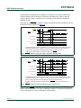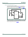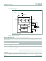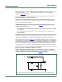
1
PCF50633
Power supply and battery management controller
Rev. 06 — 05 March 2008
User manual
Document information
Info
Content
Keywords
PCF50633, PMU, I2C-bus, USB charger, DC-to-DC converter
Abstract
This document introduces and describes the features and operation of the
PCF50633 power supply and battery management controller
PCF50633
NXP Semiconductors
PCF50633 User Manual
Revision history
Rev
Date
Description
06
20080305
Supersedes PCF50633_5
Modifications
•
File prepared for worldwide distribution.
05
20080128
Supersedes PCF50633_4
Modifications
•
Min. value for AUTO parameter VO changed from VO(prog) − 3 to VO(prog) − 5 (Table 47).
04
20071127
Supersedes PCF50633_3
Modifications
•
•
•
•
Application diagram revised (Figure 61)
HCLDO min. programmable o/p voltage value changed from 1.0 V to 0.9 V (Table 2, Table 75 and Table 88)
USB current limit (Ilim(USBx)): min./typ. values changed from 900/950 to 800/900 respectively when limit set to 1000 mA
and from 425/462 to 400/450, respectively, when limit set to 500 mA (Table 91)
Voltage drop across the USB-SYS FET (ΔVUSB-SYS) changed from 200 mV to 235 mV (Table 91).
03
20070720
Supersedes PCF50633_2
Modifications
•
•
•
•
HUQFN68 and HUQFN88 packages discontinued
Error in package layout drawing corrected (B1 = 0.20, 0.16; Figure 62)
Parameter values updated
Soldering guidelines updated.
02
20061030
Supersedes PCF50633_1
Modifications
•
•
•
•
The format of this user manual has been redesigned to comply with the new identity guidelines of NXP Semiconductors
Legal texts have been adapted to the new company name where appropriate
Updated to incorporate changes since initial release
HUQFN68 and HUQFN88 packages added.
01
20051214
Initial version
Contact information
For additional information, please visit: http://www.nxp.com
For sales office addresses, please send an email to: [email protected]
PCF50633UM_6
User manual
© NXP B.V. 2008. All rights reserved.
Rev. 06 — 05 March 2008
2 of 125
PCF50633
NXP Semiconductors
PCF50633 User Manual
1. Introduction
The PCF50633 is a highly integrated solution providing power supply generation and
battery management for mobile devices such as portable media players. It contains linear
and switching regulators, including an automatic up/down converter for hard disk supply.
Other features include a complete USB-compliant battery charger, system control
functions and a multi-purpose Analog-to-Digital Converter (ADC). The device can be
controlled by a host controller via an I2C-bus serial interface.
This document describes the features and operation of the PCF50633 and contains all the
information, including interface and connection details, required to integrate the IC into a
mobile device.
2. Features
2.1 System control
•
•
•
•
•
•
I2C-bus interface enabling extended control over all modules
State machine ensuring optimal activity in each device state
Programmable start-up and shutdown sequencer
Real Time Clock including 32768 Hz oscillator and alarms
Interrupt controller
Wake-up possibilities at 6 pins allowing wake-up by push button, slide switch and
adapter/USB insertion
• Three General Purpose I/Os (GPIO) and one high-current General Purpose Output
(GPO)
• 8-byte general purpose memory
• Ambient light sensor
• Thermal protection.
2.2 Supplies
• Auto step-up/step-down converter (1.1 A, 1.7 MHz, internal switches) for a hard disk
• Step-down converter (500 mA, 1.7 MHz, internal switches) for a CPU
• Step-down converter (500 mA, 1.7 MHz, internal switches) for memory, plus parallel
Low Dropout Regulator (LDO) for standby mode
•
•
•
•
•
•
•
•
Backlight boost converter, incorporating intensity and on/off ramp control
Seven linear regulators (4 x 50 mA, 2 x 150 mA, 1 x 200 mA with current limiting)
Dynamic voltage management on both step-down converters
Programmable inrush current on all switching regulators
On/off and output voltage control by software (I2C) and via control pins (GPIOs)
Power failure detection on most outputs
Outputs pulled down to ground when supplies are off (except LED converter)
Linear regulators can be used as switches.
PCF50633UM_6
User manual
© NXP B.V. 2008. All rights reserved.
Rev. 06 — 05 March 2008
3 of 125
PCF50633
NXP Semiconductors
PCF50633 User Manual
2.3 Battery management
• Battery charge and play system:
– Supports single-cell Li-Ion batteries
– Separate adapter and current-limited USB inputs
– Application can operate from external source when battery is low or not connected
– Battery remains fully charged after charging as long as an external power supply is
connected
– Programmable precharge and fast charge currents
– Integrated power transistors
– Thermal regulation loop controls charge rate at maximum device temperature
• Undervoltage lockout detectors with programmable thresholds
• Backup battery input for RTC supply when main battery is empty
• Backup battery charger.
2.4 ADC
•
•
•
•
10-bit resolution
4 input pins
Analog preprocessor offering input voltage division and subtraction
Direct and ratiometric measurement modes.
3. Applications
•
•
•
•
Hard disk-based portable media players
Flash-based portable media players
PDAs
Smartphones.
PCF50633UM_6
User manual
© NXP B.V. 2008. All rights reserved.
Rev. 06 — 05 March 2008
4 of 125
PCF50633
NXP Semiconductors
PCF50633 User Manual
4. Quick reference data
Table 1.
Quick reference data
VSS = REFGND = GND = 0 V; Tamb = −40 to +85 °C; unless otherwise specified.
Symbol
Parameter
Conditions
Min
Typ
Max Unit
VSYS
system supply voltage
Active mode
2.8
-
5.3
V
VBAT
battery supply voltage
Active mode
2.8
-
5
V
VBUBAT
backup battery supply voltage
1.6
-
3
V
VADAPTSNS
voltage on pin ADAPTSNS
4
-
5.3
V
VUSB
USB supply voltage
voltage on pin ADAPTSNS
4
-
5.3
V
VVISA
voltage on pin
VISA[1]
-
2.4
-
V
VVISC
voltage on pin VISC[1]
-
2.4
-
V
-
0.9
-
V
5
-
18
V
REFC[1]
VREFC
voltage on pin
VO(LED)
LED output voltage
fSW(PWM)
PWM switching frequency
for DOWN1, DOWN2 and AUTO
converters
-
1.7
-
MHz
fSW(PFM)
PFM switching frequency
for LED boost converter
-
-
1
MHz
Tth(die)
die threshold temperature
-
125
-
°C
Vth(batok)
battery OK threshold
voltage[2]
range; programmable in 100 mV steps 2.8
-
3.4
V
Vth(sysok)
system OK threshold voltage[3]
range; programmable in 100 mV steps 2.8
-
3.4
V
-
2.5
-
V
1.7
2
2.3
V
1.3
1.6
V
Vth(sysmin)
minimum system ON threshold
voltage[4]
state[5]
Vth(syspres)
system threshold voltage for save
no backup battery
Vth(bubpres)
backup battery threshold voltage for save
state[6]
1
Vth(adaptpres)
adapter presence threshold voltage
3.25 3.6
3.95 V
Vth(usbpres)
USB adapter presence threshold voltage
3.25 3.6
3.95 V
IDD(tot)
total supply current
in Save state; VBAT = 2.5 V; no USB or
adapter present
-
-
50
μA
in Standby state; all supplies disabled;
VBAT = 3.6 V; no USB or adapter
present
-
-
60
μA
in Active state; all supplies enabled
(no load); VBAT = 3.6 V; no USB or
adapter present
-
-
1
mA
[1]
Note that VVISA, VVISC and VREFC are internal signals. Pins VISA, VISC and REFC are provided to allow external decoupling capacitors
to be connected. Decoupling is necessary to ensure stable operation.
[2]
If a USB supply is connected and USBBATCHK = 1, a transition from Save to Standby will only occur if VBAT > Vth(batok) and VSYS >
Vth(sysok). A transition from Standby to Save will occur if VBAT < Vth(batok) or VSYS < Vth(sysok).
[3]
If the system voltage drops below Vth(sysok), a lowsys interrupt is generated and the time-out timer is started. The SYSOK status bit is
reset (see Table 14 and Table 20).
[4]
If the system voltage drops below Vth(sysmin), an emergency shutdown is initiated and the system transitions to the Save state.
[5]
If the system voltage drops below Vth(syspres), and no backup battery is present (bubpres = 0; see Table 14), the system will be reset and
enter the NoPower state. If a backup battery is connected (VBUBAT > Vth(BUBPRES), the PCF50633 will continue in Save mode, powered
by the backup battery.
[6]
If the system voltage is below Vth(syspres), the system will continue to operate in the Save state as long as bubpres = 1 (VBUBAT >
Vth(bubpres); see Table 14). If bubpres changes to 0, the system will be reset and enter the NoPower state.
PCF50633UM_6
User manual
© NXP B.V. 2008. All rights reserved.
Rev. 06 — 05 March 2008
5 of 125
PCF50633
NXP Semiconductors
PCF50633 User Manual
Table 2:
Overview power supplies
VSS = REFGND = GND = 0 V; Tamb = −40 to +85 °C; unless otherwise specified.
Supply
Name
Maximum Minimum Maximum Output
output
output
output
voltage
current
voltage
voltage
step size
Switching Quiescent
frequency current
PSRR[1] Output
capacitor[2]
Inductor
Programmable power supplies
DOWN1
500 mA
0.625 V
3.00 V
25 mV
1.7 MHz
-
22 μF
4.7 μH
DOWN2
500 mA
0.625 V
3.00 V
25 mV
1.7 MHz
-
22 μF
4.7 μH
AUTO
500 mA[3]
1.80 V
3.80 V
25 mV
1.7 MHz
-
22 μF
4.7 μH
1100 mA
1.80 V
3.80 V
25 mV
1.7 MHz
-
47 μF
2.2 μH
LED
25 mA
5.0 V
18.0 V
1 mA
< 1 MHz
-
10 μF
2.2 μH
LDO1:
LDO3
50 mA
0.90 V
3.60 V
100 mV
25 μA + 2 % 60 dB
of load
470 nF
LDO4
150 mA
0.90 V
3.60 V
100 mV
470 nF
LDO5
150 mA
0.90 V
3.60 V
100 mV
70 μA + 2 % 60 dB
of load
60 dB
LDO6
50 mA
0.90 V
3.60 V
100 mV
25 μA + 2 % 60 dB
of load
470 nF
HCLDO
200 mA[4]
0.90 V
3.60 V
100 mV
70 μA + 2 % 60 dB
of load
470 nF
MEMLDO
1 mA
0.90 V
3.60 V
100 mV
5 μA
[5]
60 dB
470 nF
[1]
Typical values assuming 100 Hz < f < 1000 Hz.
[2]
Typical values assuming X7R type ceramic capacitor.
[3]
Smaller external components can be used in the 500 mA configuration; the AUTOLXA2 and AUTOLXB1 pins must remain
unconnected in this configuration (see Section 8.9.6.3).
[4]
Current limited; output limited to 175 % of the max current (or 350 mA); module is switched off after a programmable debounce time
when current exceeds specified limit; afterwards, the On/Off Controller will regularly try to power up the module again (see
Section 8.11.6.2).
[5]
Output available at the DOWN2FB pin.
5. Ordering information
Table 3.
Ordering information
Type number
PCF50633HN/xx/N3[1]
[1]
Package
Name
Description
Version
HVQFN68
plastic, thermal enhanced, very thin quad flat package; no leads;
68 terminals; body 8 x 8 x 0.85 mm
SOT852-2
‘xx’ indicates the IC variant.
PCF50633UM_6
User manual
© NXP B.V. 2008. All rights reserved.
Rev. 06 — 05 March 2008
6 of 125
PCF50633
NXP Semiconductors
PCF50633 User Manual
6. Functional Diagram
ADCIN1
ADCIN2
ACCSW
NTCSW
BATSNS
9
10
8
2
10-bit ADC
LDO1
LDO2
1
LDO3
BATTEMP
ADAPTCTRL
ADAPTSNS
CHGCUR
USB1
USB2
BAT1
BAT2
SYS1
SYS2
68
LDO4
67
52
LDO1OUT
53
LDO12IN
54
55
LDO3OUT
56
LDO34IN
57
VISA
REFC
65
PCF50633
LDO1
60
61
62
LDO2
Main Battery
Charger (MBC)
5
LDO5OUT
6
LDO56IN
7
4
63
HCLDO
3
58
59
47
64
11
13
System/HDD
Auto Up/Down
Converter
(AUTO)
Internal Supply &
Reference
48
45
44
41
43
BUBAT
OSCI
OSCO
CLK32K
SCL
SDA
RSTHC
LDO4OUT
66
46
VISC
LDO2OUT
49
42
Backup Battery Charger
25
51
Core Buck
Converter
(DOWN1)
50
20
32 kHz Oscillator
19
18
Serial IF
21
Reset Generator
17
Interrupt Control
8-byte
memory
26
27
24
Memory Buck
Converter
(DOWN2)
23
22
LDO6OUT
HCLDOIN
HCLDOOUT
AUTOIN1
AUTOIN2
AUTOLXA1
AUTOLXA2
AUTOLXB1
AUTOLXB2
AUTOOUT1
AUTOOUT2
DOWN1LX
DOWN1IN
DOWN1FB
DOWN2LX
DOWN2IN
DOWN2FB
MEMLDO
IRQ
SHUTDOWN
KEEPACT
ONKEY
EXTON1
EXTON2
EXTON3
GPIO1
GPIO2
GPIO3
GPO
REFGND
VSS
39
29
38
31
LED Boost
Converter
(LED)
40
35
36
Parallel IF
30
33
34
37
LEDIN
LEDLX
LEDOUT
LEDFB
LEDFBGND
16
15
Ambient Light
Monitor
14
32
LEDAMB
28
12
Fig 1. Functional diagram of the PCF50633
PCF50633UM_6
User manual
© NXP B.V. 2008. All rights reserved.
Rev. 06 — 05 March 2008
7 of 125
PCF50633
NXP Semiconductors
PCF50633 User Manual
7. Pinning Information
BATTEMP
ADAPTCTRL
ADAPTSNS
CHGCUR
VISC
BAT2
BAT1
USB2
USB1
SYS2
SYS1
LDO4OUT
LDO34IN
LDO3OUT
LDO2OUT
LDO12IN
LDO1OUT
67
66
65
64
63
62
61
60
59
58
57
56
55
54
53
52
terminal 1
index area
68
7.1 Pinning
BATSNS
1
51
OSCI
NTCSW
2
50
OSCO
HCLDOOUT
3
49
BUBAT
HCLDOIN
4
48
AUTOLXA1
LDO5OUT
5
47
AUTOIN1
LDO56IN
6
46
AUTOIN2
LDO6OUT
7
45
AUTOLXA2
ACCSW
8
44
AUTOLXB1
ADCIN1
9
43
AUTOOUT1
ADCIN2
10
42
AUTOOUT2
VISA
11
41
AUTOLXB2
REFGND
12
40
ONKEY
REFC
13
39
SHUTDOWN
GPIO3
14
38
KEEPACT
GPIO2
15
37
EXTON3
GPIO1
16
36
EXTON2
IRQ
17
35
EXTON1
18
19
20
21
22
23
24
25
26
27
28
29
30
31
32
33
34
SDA
SCL
CLK32K
RSTHC
DOWN2FB
DOWN2IN
DOWN2LX
DOWN1LX
DOWN1IN
DOWN1FB
GPO
LEDIN
LEDOUT
LEDLX
LEDAMB
LEDFB
LEDFBGND
PCF50633
SOT852-2
Transparent top view
(1) The VSS terminal is connected to the package exposed diepad and must be connected to
ground.
(2) This diagram is a top view. The exposed diepad is visible from the bottom only.
(3) Pin 1 is indicated with a dot in the upper left corner.
(4) See Section 13 for a mechanical specification the HVQFN68 package.
Fig 2. Pin configuration for HVQFN68 package
7.2 Pin description
Table 4.
Symbol
Pin description
Pin
Description
Control interfaces
ONKEY
40
active-LOW ‘on’ key input with internal pull-up resistor
EXTON1
35
external activation (wake-up) input
EXTON2
36
external activation (wake-up) input
EXTON3
37
external activation (wake-up) input
PCF50633UM_6
User manual
© NXP B.V. 2008. All rights reserved.
Rev. 06 — 05 March 2008
8 of 125
PCF50633
NXP Semiconductors
PCF50633 User Manual
Table 4.
Pin description …continued
Symbol
Pin
Description
RSTHC
21
active-LOW reset output for host controller; open-drain output
CLK32K
20
32.768 kHz digital clock output; open-drain output
GPIO1
16
GPIO2
15
GPIO3
14
input mode: control signal inputs with programmable impact on activity
of regulators.
output mode: general purpose open-drain outputs
GPO
28
general purpose push-pull output
SHUTDOWN
39
shuts down the PCF50633 when a LOW-to-HIGH transition is detected
IRQ
17
interrupt request to host controller; this active-LOW signal has an
open-drain output
KEEPACT
38
Active state continuation input
SCL
19
I2C-bus interface clock
SDA
18
I2C-bus interface data
Linear and switching regulators
AUTOIN1[1]
47
DC-to-DC auto up/down converter input 1
AUTOIN2[1]
46
DC-to-DC auto up/down converter input 2
AUTOLXA1[2]
48
inductor connection 1 to buck part of DC-to-DC auto up/down
converter
AUTOLXA2[2] 45
inductor connection 2 to buck part of DC-to-DC auto up/down
converter
AUTOLXB1[2] 44
inductor connection 1 to boost part of DC-to-DC auto up/down
converter
AUTOLXB2[2] 41
inductor connection 2 to boost part of DC-to-DC auto up/down
converter
AUTOOUT1[1] 43
DC-to-DC auto up/down converter output 1
AUTOOUT2[1] 42
DC-to-DC auto up/down converter output 2
DOWN1IN
26
DC-to-DC step-down converter 1 input
DOWN1FB
27
DC-to-DC step-down converter 1 feedback input
DOWN1LX
25
inductor connection to DC-to-DC step-down converter 1
DOWN2IN
23
DC-to-DC step-down converter 2 input
DOWN2FB
22
DC-to-DC step-down converter 2 feedback input and MEMLDO output
DOWN2LX
24
inductor connection to DC-to-DC step-down converter 2
LEDIN
29
LED boost converter input
LEDLX
31
inductor connection to LED boost converter
LEDOUT
30
current-controlled output of LED boost converter
LEDFB
33
feedback for current loop of LED boost converter
LEDFBGND
34
feedback ground sense input to LED boost converter
LEDAMB
32
ambient light sensor input
LDO12IN
53
shared input for LDO1 and LDO2 linear regulators
LDO1OUT
52
LDO1 linear regulator output
LDO2OUT
54
LDO2 linear regulator output
LDO34IN
56
shared input for LDO3 and LDO4 linear regulators
LDO3OUT
55
LDO3 linear regulator output
PCF50633UM_6
User manual
© NXP B.V. 2008. All rights reserved.
Rev. 06 — 05 March 2008
9 of 125
PCF50633
NXP Semiconductors
PCF50633 User Manual
Table 4.
Pin description …continued
Symbol
Pin
Description
LDO4OUT
57
LDO4 linear regulator output
LDO56IN
6
shared input for LDO5 and LDO6 linear regulators
LDO5OUT
5
LDO5 linear regulator output
LDO6OUT
7
LDO6 linear regulator output
HCLDOIN
4
high-current linear regulator input
HCLDOOUT
3
high-current linear regulator output
32.768 kHz oscillator
OSCI
51
32.768 kHz oscillator input
OSCO
50
32.768 kHz oscillator output
Internal supply
REFC
13
reference voltage; bypass capacitor connection
VISA
11
internal analog supply voltage decoupling node
VISC
64
internal analog supply voltage decoupling node
Battery charger
USB1[1]
60
USB2[1]
61
USB power input 2
BAT1[1]
62
battery terminal 1
BAT2[1]
63
battery terminal 2
BATSNS
1
battery voltage sense input
SYS1[1]
58
system and adapter connection terminal 1
SYS2[1]
59
system and adapter connection terminal 2
ADAPTSNS
66
adapter sense input
ADAPTCTRL
67
adapter switch gate drive output
USB power input 1
BATTEMP
68
battery temperature sense input
CHGCUR
65
charger current reference resistor connection
BUBAT
49
backup battery connection
ADC
ADCIN1
9
ADC channel 1 input
ADCIN2
10
ADC channel 2 input
NTCSW
2
battery temperature resistor bridge connection
ACCSW
8
accessory resistor bridge connection
REFGND
12
reference ground
VSS
backplane power ground connection
Ground
[1]
The following pin pairs must be connected on the PCB:
AUTOIN1 to AUTOIN2
AUTOOUT1 to AUTOOUT2
USB1 to USB2
BAT1 to BAT2
SYS1 to SYS2
These pins are all power pins. They must be connected via a low-ohmic connection.
PCF50633UM_6
User manual
© NXP B.V. 2008. All rights reserved.
Rev. 06 — 05 March 2008
10 of 125
PCF50633
NXP Semiconductors
PCF50633 User Manual
[2]
For the AUTO converter, in the 1.1 A configuration, the following pin pairs must be connected on the PCB:
AUTOLXA1 to AUTOLXA2
AUTOLXB1 to AUTOLXB2
The AUTOLXA2 and AUTOLXB1 pins must remain unconnected in the 500 mA configuration (see
Section 8.9.6.3). These pins are all power pins. They must be connected via a low-ohmic connection.
8. Functional description
8.1 On/Off Control (OOC)
8.1.1 Introduction
The OOC controls the activity states of the PCF50633. It also provides sequencing for the
host controller clock (CLK32K) and reset (RSTHC) signals. Four programmable start-up
phases facilitate the sequential start-up of the supplies.
8.1.2 Features
•
•
•
•
•
•
Finite state machine supporting Save, Standby and Active states
Programmable wake-up condition for ONKEY and EXTONx inputs
Wake-up condition for RTC alarm
Programmable sequencing for host controller clock (CLK32K) and reset (RSTHC)
Four separate activity phases for power supply sequencing
Programmable debounce for ONKEY, EXTONx and SHUTDOWN inputs.
8.1.3 Block diagram
OOC
Interrupts
Operating
States
sysok
batok
Activation
Phases
tmpok
ON/OFF
State
Machine
RTC alarm
EXTONx
CLK32K
RSTHC
ONKEY
SHUTDOWN
KEEPACT
I2 C
Software
Control
Fig 3. OOC block diagram
PCF50633UM_6
User manual
© NXP B.V. 2008. All rights reserved.
Rev. 06 — 05 March 2008
11 of 125
PCF50633
NXP Semiconductors
PCF50633 User Manual
8.1.4 Hardware interface
Table 5:
OOC characteristics
VSS = REFGND = GND = 0 V; Tamb = −40 to +85 °C; unless otherwise specified.
Symbol
Parameter
Conditions
Min
Typ
Max
Unit
VSYS
system supply voltage
Active mode
2.8
-
5.3
V
ILi
input leakage current
on EXTONx, KEEPACT and
SHUTDOWN pins
−1
-
+1
μA
on ONKEY pin when input HIGH
-
-
+1
μA
on ONKEY pin when input LOW
−15
−10
−5
μA
0
-
0.5
V
HIGH-level input voltage
on ONKEY, EXTONx, KEEPACT and
SHUTDOWN pins
0.8
-
5.5
V
Rpu(int)
internal pull-up resistance
on ONKEY pin
-
300
-
kΩ
VOL
LOW-level output voltage
on CLK32K and RSTHC pins; pull-up
resistance > 10 kΩ
−0.2
-
0.4
V
IOL
LOW-level output current
on RSTHC and CLK32K pins
-
-
1.5
mA
Tth(die)
die threshold temperature
-
125
-
°C
Vth(sysmin)
minimum system ON threshold
voltage[1]
-
2.5
-
V
Vth(syspres)
system threshold voltage for save
state[2]
1.7
2
2.3
V
Vth(bubpres)
backup battery threshold voltage for
save state[3]
1
1.3
1.6
V
VVISA
voltage on pin VISA[4]
-
2.4
-
V
-
0.9
-
V
in Save state; VBAT = 2.5 V; no USB
or adapter present
-
-
50
μA
in Standby state; all supplies disabled;
VBAT = 3.6 V; no USB or adapter
present
-
-
60
μA
in Active state; all supplies enabled
(no load)
-
-
1
mA
VIL
LOW-level input voltage
VIH
no backup battery
REFC[4]
VREFC
voltage on pin
IDD(tot)
total supply current
[1]
If the system voltage drops below Vth(sysmin), an emergency shutdown is initiated and the system transitions to the Save state.
[2]
If the system voltage drops below Vth(syspres), and no backup battery is present (bubpres = 0; see Table 14), the system will be reset and
enter the NoPower state. If a backup battery is connected (VBUBAT > Vth(BUBPRES), the PCF50633 will continue in Save mode, powered
by the backup battery.
[3]
If the system voltage is below Vth(syspres), the system will continue to operate in the Save state as long as bubpres = 1 (VBUBAT >
Vth(BUBPRES; see Table 14). If bubpres is reset to 0, the system will be reset and will enter the NoPower state.
[4]
Note that VVISA and VREFC are internal signals. Pins VISA and REFC are provided to allow external decoupling capacitors to be
connected. Decoupling is necessary to ensure stable operation.
8.1.5 Software interface
Table 6.
VERSION - Version ID register (address 00h) bit description
Bit
Symbol
Access Value
Description
7-0
version
R
IC version number
xxxxxxxx
PCF50633UM_6
User manual
© NXP B.V. 2008. All rights reserved.
Rev. 06 — 05 March 2008
12 of 125
PCF50633
NXP Semiconductors
PCF50633 User Manual
Table 7.
VARIANT - Version ID register (address 01h) bit description
Bit
Symbol
Access Value
Description
7-0
variant
R
ROM number to distinguish PCF50633 variants with
different reset values
Table 8.
Bit
xxxxxxxx
OOCSHDWN - OOC shutdown register (address 0Ch) bit description
Symbol
Access
Reset
Description
0
go_stby
R/W[2]
0
0: no action
1: initiates a transition to Standby
1
reserved
2
totrst
R/W[2]
0
0: no action
1: resets time-out timer
3
coldboot
R/W
1
0: no coldboot condition
1: coldboot; device has been in NoPower state
7:4
reserved
[1]
Register is reset in NoPower state.
[2]
Bit is cleared after transition.
Table 9.
OOCWAKE - OOC wake-up register (address 0Dh) bit description
Bit
Symbol
Access
Reset[1]
Description
0
onkey_wake
R
1
0: ONKEY functionality disabled
1: ONKEY functionality enabled
1
exton1_wake R
1
0: EXTON1 functionality disabled
1: EXTON1 functionality enabled
2
exton2_wake R/W
1
0: EXTON2 functionality disabled
1: EXTON2 functionality enabled
3
exton3_wake R/W
1
0: EXTON3 functionality disabled
1: EXTON3 functionality enabled
4
rtc_wake
R/W
1
0: wake-up by RTC alarm disabled
1: wake-up by RTC alarm enabled
5
reserved
6
usb_wake
R/W
1
0: wake-up by USB insert disabled
1: wake-up by USB insert enabled
7
adp_wake
R/W
1
0: wake-up by adapter insert disabled
1: wake-up by adapter insert enabled
[1]
Register is reset in NoPower state.
Table 10.
OOCTIM1 - OOC debounce register 1 (address 0Eh) bit description
Bit Symbol
Access Reset[1] Description
1:0 exton1_deb R/W
10
debounce time for EXTON1
00: none 01: 5 ms,
10: 14 ms 11: 62 ms
3:2 exton2_deb R/W
10
debounce time for EXTON2 (timing same as for bits 1:0)
5:4 exton3_deb R/W
10
debounce time for EXTON3 (timing same as for bits 1:0)
7:6 shdwn_deb R/W
10
debounce time for SHUTDOWN (timing same as for bits 1:0)
[1]
Register is reset in NoPower state.
PCF50633UM_6
User manual
[1]
© NXP B.V. 2008. All rights reserved.
Rev. 06 — 05 March 2008
13 of 125
PCF50633
NXP Semiconductors
PCF50633 User Manual
Table 11.
OOCTIM2 - OOC debounce register 2 (address 0Fh) bit description
Bit
Symbol
Access Reset[1]
Description
2:0
onkey_deb
R/W
010
debounce time for ONKEY
000: none
001: 5 ms
010: 14 ms
011: 62 ms
100: 200 ms
101: 500 ms
110: 1000 ms
111: 2000 ms
4:3
actphdel
R/W
01
delay between activation phases
00 : 5 ms
01 : 10 ms
10 : 15 ms
11 : 20 ms
6:5
hcrstdel
R/W
10
delay between selected activation phase and host
controller reset
00 : 3 ms
01 : 6 ms
10 : 13 ms
11 : 26 ms
7
almon
R/W
0
0: ambient light monitor disabled
1: ambient light monitor enabled
[1]
This register is reset at each transition to Standby state.
Table 12.
OOCMODE - OOC mode register (address 10h) bit description[1]
Bit
Symbol
Access Description
1:0
exton1_mode
R/W
EXTON1 mode selection
00: wake-up on falling edge only
01: wake-up on rising edge only
10: wake-up on falling edge only; rising edge sets the time-out
timer to 8 seconds
11: wake-up on rising edge only; falling edge sets the time-out
timer to 8 seconds
3:2
exton2_mode
R/W
EXTON2 mode selection
behavior like exton1_mode
5:4
exton3_mode
R/W
EXTON3 mode selection
behavior like exton1_mode
7:6
onkey_mode
R
ONKEY mode selection
00: wake-up on falling edge only
01: wake-up on falling edge; sets the time-out timer to 8
seconds if held LOW for 1 second
10: wake-up on falling edge only; rising edge sets the time-out
timer to 8 seconds
11: reserved
[1]
This register is reset in NoPower state. Reset values are determined by the IC variant (see Table 7).
PCF50633UM_6
User manual
© NXP B.V. 2008. All rights reserved.
Rev. 06 — 05 March 2008
14 of 125
PCF50633
NXP Semiconductors
PCF50633 User Manual
Table 13.
OOCCTL - OOC control register (address 11h) bit description[1]
Bit
Symbol
Access Description
1:0
actphrst
R/W
selects activity phase to which host controller reset is related
00: related to activation phase 1
01: related to activation phase 2
10: related to activation phase 3
11: related to activation phase 4
2
actclk32on
R/W
0: CLK32K output disabled in Active state
1: CLK32K output enabled in Active state
3
heartbeat
R/W
0: KEEPACT input requires DC HIGH
1: KEEPACT input requires toggling input to retain Active state
4
usbbatchk
R/W
0: VBAT status has no effect on state machine
1: VBAT must be > Vth(batok) to go to Standby state
5
reserved
6
stbclk32on
R/W
0: CLK32K output disabled in Standby state
1: CLK32K output enabled in Standby state
7
reserved
[1]
This register is reset in NoPower state. Reset values are determined by the IC variant (see Table 7).
Table 14.
OOCSTAT - OOC status register (address 12h) bit description
Bit
Symbol
Access
Description
0
onkey
R
0: ONKEY voltage is below threshold
1: ONKEY voltage is above threshold
1
exton1
R
0: EXTON1 voltage is below threshold
1: EXTON1 voltage is above threshold
2
exton2
R
0: EXTON2 voltage is below threshold
1: EXTON2 voltage is above threshold
3
exton3
R
0: EXTON3 voltage is below threshold
1: EXTON3 voltage is above threshold
4
bubpres
R
0: VBUBAT < Vth(bubpres)
1: VBUBAT > Vth(bubpres)
5
sysok
R
0: VSYS < Vth(sysok)
1: VSYS > Vth(sysok)
6
batok
R
0: VBAT < Vth(batok)
1: VBAT > Vth(batok)
7
tmpok
R
0: die temperature > Tth(die)
1: die temperature < Tth(die)
8.1.6 Functional description
8.1.6.1
Activity states
From the perspective of on/off control, the PCF50633 is composed of a charger and a
power management unit. The charger operates autonomously; it charges the battery
when necessary, provided charging is possible. It also delivers the system voltage
required by the power management unit.
PCF50633UM_6
User manual
© NXP B.V. 2008. All rights reserved.
Rev. 06 — 05 March 2008
15 of 125
PCF50633
NXP Semiconductors
PCF50633 User Manual
External Adapt-SYS PFET
Adapter
USBx
Power management
USB
charger
Adapter
charger
Ideal
diode
Output control,
Supplies,
ADC etc.
Application
SYSx
Charger
BUBAT
BATx
Main
battery
Backup
battery
Fig 4. Charger and power management partitioning
The power management unit features 4 activity states:
• NoPower
In the NoPower state both the system and the backup battery voltages are below their
presence threshold levels (VSYS < Vth(syspres) and VBUBAT < Vth(bubpres); see Figure 6).
There is insufficient energy available to power any of the internal circuits. The system
will change state from NoPower to Save when VSYS rises above Vth(sysmin).
• Save
In the Save state, the power management section is supplied from either the system
voltage (if VSYS > Vth(syspres)) or the backup battery (if VSYS < Vth(syspres) and
VBUBAT > Vth(bubpres); see Figure 6). Only the internal supplies, the 32 kHz oscillator
and the real-time clock will be active. The GPIOs will maintain their state. If both the
system and the backup battery voltages fall below there presence threshold levels
(VSYS < Vth(syspres) and VBUBAT < Vth(bubpres)), the PCF50633 will revert to the NoPower
state.
• Standby
In Standby state, the power management section is supplied by the system voltage,
which will be above its OK threshold level (Vth(sysok) is specified by the svmlvl bits in
the SVMCTL control register; see Table 35). All monitoring and internal control
functions in the PCF50633 are activated. Most power supplies remain off, but all LDOs
(LDO1 through LDO6, MEMLDO and HCLDO) may be enabled if required (see
Table 15 and Section 8.8.5). If VSYS falls below Vth(sysok), the PCF50633 will revert to
the Save state.
• Active
The PCF50633 is fully functional in the Active state. The host controller has full control
through the serial I2C-bus interface.
Table 15 describes module activity in each state while Figure 5 illustrates the PCF50633
state diagram.
PCF50633UM_6
User manual
© NXP B.V. 2008. All rights reserved.
Rev. 06 — 05 March 2008
16 of 125
PCF50633
NXP Semiconductors
PCF50633 User Manual
Table 15.
Activity states and module activity
Device state
Modules always on
Modules programmable
ON or OFF
Modules always off
NoPower
None
None
All
Save
OSC32, RTC,
INT, GPIO
None
Others
Standby
OSC32, RTC,
INT, GPIO, SVM
LDO1-LDO6, HCLDO,
MEMLDO, BVM, CLK32K
Others
Active
OSC32, RTC,
INT, GPIO, SVM,
BVM, I2C, THS
Others
None
PCF50633UM_6
User manual
© NXP B.V. 2008. All rights reserved.
Rev. 06 — 05 March 2008
17 of 125
PCF50633
NXP Semiconductors
PCF50633 User Manual
NOPOWER
No valid energy
source available
VSYS present
VSYS and VBUBAT
absent
SAVE
Powered from SYS if
voltage high enough,
otherwise from
backup battery
VSYS OK
VSYS not OK
STANDBY
Powered from SYS
VSYS not OK
Wake up by
EXTONx, ONKEY,
RTC alarm,
USB or adapter connect
Shutdown by
ONKEY, SHUTDOWN,
missing KEEPACT,
go_stby bit or error conditions
ACTIVE
Powered from SYS
Fig 5. PCF50633 power management state diagram
8.1.6.2
Transitions between activity states
The OOC controls the transitions between the activity states of the power management
section of the PCF50633.
PCF50633UM_6
User manual
© NXP B.V. 2008. All rights reserved.
Rev. 06 — 05 March 2008
18 of 125
PCF50633
NXP Semiconductors
PCF50633 User Manual
Active
Standby
VSYS /
VBAT
Vth(sysok) / 2.8 V Vth(batok) 3.4 V
For USB supply:
when usbbatchk is set,
transition to Standby
only if VBAT > Vth(batok)
For USB supply:
when usbbatchk is set,
transition to Save
if VBAT < Vth(batok)
lowsys Interrupt
sysok = '0'
Time-out timer on
Vth(sysmin) 2.5 V
Emergency shutdiown
Immediate transition to Save
No Interrupt
VSYS
Save
Vth(syspres) 2.0 V
bubpres = 0
(VBUBAT < Vth(bubpres)
VBUBAT
bubpres = 1
(VBUBAT > Vth(bubpres)
Vth(bubpres) 1.3 V
NoPower
Fig 6. State transitions and threshold voltages
Transition from NoPower to Save: The system will change state from NoPower to Save
when the system voltage (VSYS) rises above Vth(sysmin).
Transition from Save to NoPower: In the absence of a charged backup battery
(bubpres = 0), the system will return to the NoPower state when the system voltage falls
below Vth(syspres). If a backup battery is present (bubpres = 1), the system will return to
NoPower when the backup battery voltage falls below Vth(bubpres).
Transition from Save to Standby: The PCF50633 will change state from Save to Standby
when VSYS is greater than Vth(sysok) (specified by the svmlvl control bits in register
SVMCTL; see Table 35) and the die temperature is below the maximum temperature
threshold (Tth(die); see Section 8.6).
An additional condition may be imposed if a USB supply is connected. In this case, if bit
usbbatchk in control register OOCCTL (see Table 13) is set, the PCF50633 will only
change state from Save to Standby if VBAT is greater than Vth(batok).
Transition from Standby to Save: The PCF50633 will revert to the Save state if the
system voltage drops below Vth(sysok) or the die temperature is above the maximum
temperature threshold (Tth(die); see Section 8.6).
If a USB supply is connected, and bit usbbatchk in control register OOCCTL (see
Table 13) is set, the PCF50633 will also revert to the Save state if VBAT falls below
Vth(batok).
PCF50633UM_6
User manual
© NXP B.V. 2008. All rights reserved.
Rev. 06 — 05 March 2008
19 of 125
PCF50633
NXP Semiconductors
PCF50633 User Manual
Transition from Standby to Active: Several wake-up events will cause the PCF50633 to
switch from Standby to the Active state. Note that the response to these events is edge
sensitive:
• The user presses the ONKEY (ONKEY falling edge; see Section 8.1.6.4)
• One of the EXTONx inputs goes HIGH or LOW (depending on the configuration of the
extonx_mode control bits; see Table 12 and Section 8.1.6.5)
If a fault condition prevents the transition to Active state triggered by any of these events,
the wake-up event will be lost.
The following wake-up events will continue to be asserted as long as the event remains
active (level sensitive):
• An RTC alarm interrupt
• A high enough voltage is detected on either the USBx or ADAPTSNS pin to indicate
that a USB device or an adapter has been connected.
The RTC alarm and external power connection events remain valid as long as the
corresponding interrupt bits are set in the INT module. The interrupt bits are cleared by a
read access to the INT register.
All wake-up events can be disabled by clearing the corresponding wake control bits in the
OOCWAKE register (see Table 9). Note that interrupts are still generated.
In the Active state a subset (dependant on the reset values of the IC variant) of the power
supplies is switched on. After the supplies have become stabilized, the RSTHC output is
released allowing the host controller to start up.
Transition from Active to Standby: Transitions from Active to Standby can be direct and
immediate or can occur after an 8-second delay. In the later case, a time-out timer is
initiated and the system enters Standby after 8 seconds, providing the host controller
doesn’t intervene in the meantime.
A direct and immediate transition is initiated in the event of one of the following (error)
conditions:
• The go_stby bit in control register OOCSHDWN (see Table 8) is set. This allows the
host controller approximately 2 ms to shut down before the PCF50633 enters Standby
state.
• Absence of a valid KEEPACT signal (see Section 8.1.6.11).
• A LOW-to-HIGH transition on the SHUTDOWN pin
An 8-second time-out timer is initiated in the event of one of the following conditions. After
8 seconds, the PCF50633 enters Standby mode if no action is taken by the host controller
in the meantime:
• The ONKEY pin is LOW for longer than 1 second (if onkey_mode control bits
configured accordingly; see Table 12).
• Rising edge on ONKEY (if onkey_mode control bits configured accordingly; see
Table 12).
• Rising or falling edge on EXTONx (if extonx_mode control bits configured
accordingly; see Table 12 and Section 8.1.6.5)
PCF50633UM_6
User manual
© NXP B.V. 2008. All rights reserved.
Rev. 06 — 05 March 2008
20 of 125
PCF50633
NXP Semiconductors
PCF50633 User Manual
Transitions from Active to Save: Transitions from Active to Save can be direct and
immediate or can occur after a 1-second or an 8-second delay. In the later case, a
time-out timer is initiated and the system enters Save state after, respectively, 1 or 8
seconds if the host controller doesn’t intervene in the meantime.
A direct and immediate transition occurs when VSYS falls below the Vth(sysmin).
The following conditions initiate the time-out timer:
• lowsys interrupt when the system voltage drops below Vth(sysok) (specified by the
svmlvl control bits in register SVMCTL; see Table 35) (8-second time-out)
• hightmp interrupt when the die temperature exceeds the maximum temperature
threshold, Tth(die) (1-second time-out)
8.1.6.3
Time-out timer
PCF50633 on/off control uses a time-out timer to set up delays before responding to
several events, as discussed above in Section 8.1.6.2. The timer is set to 8 seconds for all
events other than a high die temperature event, when the timer is set to 1 second.
These delays are inserted to allow the host controller time to poll interrupts and respond to
events. The totrst bit in control register OOCSHDWN can be used to extend the delay if
necessary or to ignore the event (see Table 8). When totrst is set to 1:
• If no timer-related interrupts (interrupts that would cause the timer to be initiated) have
been generated, the timer is stopped. In this case the PCF50633 remains in the Active
state.
• If one or more timer-related interrupts have been generated but have not been read
by the host controller, the timer is reset. The delay is set to 1 or 8 seconds as
appropriate, allowing the host controller time to poll the remaining interrupts.
8.1.6.4
ONKEY control input
The ONKEY input is intended to be connected to a push button which, when pressed,
connects the input to ground. The ONKEY input has an internal pull-up resistor to ensure
the input is HIGH by default. However, it can also be used as a regular control input.
The onkey_wake control bit (bit 0 in register OOCWAKE; see Table 9) enables/disables
the ONKEY function.
A programmable debounce filter is incorporated into the ONKEY input. The debounce
time is determined by the setting of control bits onkey_deb (bits 2:0 in control register
OOCTIM2; see Table 11).
The ONKEY mode, which determines how the PCF50633 responds when the push button
is pressed, is selected via the onkey_mode control bits (bits 7:6 in control register
OOCMODE; see Table 12).
Three interrupts (onkeyf, onkeyr and onkey1s) are generated when the push button is
pressed and released, as illustrated in Figure 7 and Figure 8.
A transition from Active to Standby in response to an ONKEY event is interrupt driven.
PCF50633UM_6
User manual
© NXP B.V. 2008. All rights reserved.
Rev. 06 — 05 March 2008
21 of 125
PCF50633
NXP Semiconductors
PCF50633 User Manual
Note that if the PCF50633 goes to Standby in response to an onkey1s interrupt, the
interrupt register must be read the next time the chip starts up in order to clear the
onkey1s interrupt. If this is not done, the next onkey1s interrupt-driven transition to
Standby will fail.
The status of the ONKEY pin (HIGH or LOW) can be determined by reading bit 0 of the
OOCSTAT control register (see Table 14).
ONKEY
tdebounce
ONKEY debounced
onkeyf interrupt
tdebounce
onkeyr interrupt
onkey1s interrupt
system state
Standby
Active
The debounced signal retains its original value until the new value has been stable for at least
the selected debounce time. A spike (> 30 μs) in the original signal will reset the debounce
timer. The filter suppresses all signal activity shorter than the debounce time.
A Standby-to-Active transition is initiated by pressing the ONKEY
Fig 7. ONKEY behavior when push button pressed in Standby state
ONKEY
tdebounce
ONKEY debounced
onkeyf interrupt
tdebounce
onkeyr interrupt
1s
onkey1s interrupt
system state
8 second timeout
Active
Standby
The debounced signal retains its original value until the new value has been stable for at least
the selected debounce time. A spike (> 30 μs) in the original signal will reset the debounce
timer. The filter suppresses all signal activity shorter than the debounce time.
An Active-to-Standby transition is initiated when the ONKEY push button is held down for 1
second.
Fig 8. ONKEY behavior when push button pressed in Active state
Note that if the ONKEY push button is held down for more than one second during the
ONKEY wake-up transition, an Active-to-Standby transition is not initiated (the time-out
timer is not set and an onkey1s interrupt is not generated).
PCF50633UM_6
User manual
© NXP B.V. 2008. All rights reserved.
Rev. 06 — 05 March 2008
22 of 125
PCF50633
NXP Semiconductors
PCF50633 User Manual
8.1.6.5
EXTON control inputs
Three inputs are provided to facilitate external activation. The EXTONx inputs are
intended to be connected to a variety of wake-up sources, such as an active user
interface or external connectors. They can be configured to initiate either wake-up or
shutdown transitions (via the extonx_mode control bits in the OOCMODE register; see
Table 12).
Each of the extonx_wake control bits (bits 3:1 in control register OOCWAKE; see Table 9)
enables/disables its respective EXTONx input. The inputs, EXTON1, EXTON2 and
EXTON3, are functionally identical.
Programmable debounce filters are incorporated into the EXTONx inputs. The debounce
time is determined by the setting of the extonx_deb control bits (bits 5:0 in control register
OOCTIM1; see Table 10).
The status of the EXTONx pins (HIGH or LOW) can be determined by reading bits 3:1 of
the OOCSTAT control register (see Table 14).
Two interrupts (extonxr and extonxf; see Table 18) are generated in response to activity
on each of the EXTONx inputs as illustrated in Figure 9.
EXTONx
tdebounce
EXTONx debounced
extonxr interrupt
tdebounce
extonxf interrupt
system state
Standby
Active
The debounced signal retains its original value until the new value has been stable for at least
the selected debounce time. A spike (> 30 μs) in the original signal will reset the debounce
timer. The filter suppresses all signal activity shorter than the debounce time
wake-up on rising edge of EXTONx input (extonx_mode = 01)
Fig 9. EXTON behavior
8.1.6.6
SHUTDOWN control input
When a positive edge is detected on the SHUTDOWN input, a transition from Active to
Standby is initiated.
The SHUTDOWN input features a programmable debounce filter. The debounce time is
determined by the setting of control bits shdwn_deb (bits 7:6 in control register OOCTIM1;
see Table 10).
8.1.6.7
go_stby bit
Writing 1 to the go_stby control bit initiates a transition from Active to Standby state (bit 0
in control register OOCSHDWN; Table 8).
PCF50633UM_6
User manual
© NXP B.V. 2008. All rights reserved.
Rev. 06 — 05 March 2008
23 of 125
PCF50633
NXP Semiconductors
PCF50633 User Manual
A 2 ms delay is inserted between the write operation and the disabling of activation phase
4 (ACTPH4; see Section 8.1.6.8 below). This allows the host controller to perform any
necessary housekeeping tasks. Figure 10 shows a timing diagram for a shutdown
sequence in response to 1 being written to go_stby.
Activity State
ACTPH4
ACTPH3
ACTPH2
ACTPH1
STANDBY
Programming
go_stby control bit
2 ms
Fig 10. GO_STBY timing
8.1.6.8
Activity phases
There are 4 distinct phases involved in a state transition to or from the Active state (see
Figure 10 above). This is necessary to enable power supply and reset signal sequencing.
The actphdel control bits (bits 4:3 in control register OOCTIM2; see Table 11) set the
delay between the phases. The ACTPH1 to ACTPH4 signals are available as GPIO or
GPO outputs.
The sequence is followed for all shutdown conditions with the exception of an emergency
shutdown (VSYS < Vth(sysmin)), in which case there is an immediate transition to the Save
state.
Wake-up
event
Shutdown
event
ACTPH1
ACTPH2
ACTPH3
ACTPH4
tphdel
tphdel
tphdel
tphdel
tphdel
tphdel
CLK32K
RSTHC
trstdel
Fig 11. Activity phases during transition to and from the Active state
PCF50633UM_6
User manual
© NXP B.V. 2008. All rights reserved.
Rev. 06 — 05 March 2008
24 of 125
PCF50633
NXP Semiconductors
PCF50633 User Manual
8.1.6.9
Reset outputs
The RSTHC output signal is intended to drive the reset input of the host controller. It is
synchronized with one of the activity phases discussed above in Section 8.1.6.8 and then
released (pulled HIGH) after a pre-determined period, trsdel, of between 3 and 26 ms (trsdel
allows time for the supply to the host controller to stabilize before the reset signal is
released).
The activity phase is selected by the actphrst control bits (bits 1:0 in register OOCCTL;
see Table 13) and the delay (trsdel) by the hcrstdel control bits (bits 6:5 in register
OOCTIM2; see Table 11).
The RSTHC output pin is open drain, requiring an external pull up resistor. The
synchronization and timing of the RSTHC signal is illustrated in the bottom trace of
Figure 11 (actphrst = 10).
When the voltage on the SYS pin drops below Vth(sysmin) (emergency shutdown), RSTHC
goes LOW immediately in order to shut down the host controller.
8.1.6.10
CLK32K output
A 32.678 Hz system clock is available on the CLK32K pin when activated. The clock can
be activated in Standby or Active states by setting stbclk32on or actclk32on, respectively,
in the OOCCTL control register (see Table 13). In the Active state, the activation of the
clock is synchronized with ACTPH1, as shown in Figure 11.
The CLK32K pin has an open drain output, allowing the appropriate voltage swing to be
generated externally. A typical value for an external pull-up resistor is 100 kΩ.
8.1.6.11
KEEPACT input
The KEEPACT input is intended to ensure that the host controller remains active while the
PCF50633 is in Active state. However, it can also be used by an external circuit to force a
transition from Active to Standby.
KEEPACT supports two modes:
• Keepact mode: after a transition from Standby to Active the PCF50633 expects the
KEEPACT input to be forced HIGH by the host controller. If this does not happen
within 100 ms of RSTHC going HIGH, the PCF50633 reverts to Standby.
• Heartbeat mode: after a transition from Standby to Active the PCF50633 expects the
KEEPACT signal to toggle at least every 500 ms. If this does not happen, the
PCF50633 reverts to Standby.
Regular Keepact mode is selected by default. Heartbeat mode is selected when the
heartbeat control bit in the OOCCTL register is set (see Table 13).
KEEPACT timing is illustrated in Figure 12 and Figure 13.
PCF50633UM_6
User manual
© NXP B.V. 2008. All rights reserved.
Rev. 06 — 05 March 2008
25 of 125
PCF50633
NXP Semiconductors
PCF50633 User Manual
System
state
Standby
Standby
Active
RSTHC
KEEPACT
100 ms(1)
(1) The KEEPACT signal must be set in this interval to maintain the Active state
Fig 12. KEEPACT timing (Keepact mode)
System
state
Standby
Standby
Active
RSTHC
KEEPACT
500 ms(1)
(1) The KEEPACT signal must toggle in this interval to maintain the Active state
Fig 13. KEEPACT timing (Heartbeat mode)
The default reset KEEPACT mode is variant dependent (see Table 7).
8.1.6.12
Debounce filters
Many control signals in the PCF50633 can be debounced to avoid responding to signal
spikes. Debounce filters are enabled in all states. Debounce times are programmable.
The timing diagram in Figure 14 applies to all debounce filters in the PCF50633.
undebounced
tdebounce
tdebounce
debounced
interrupts
falling edge
rising edge
The debounced signal retains its original value until the new value has been stable for at least
the selected debounce time. A spike (> 30 ms) in the original signal will reset the debounce
timer. The filter suppresses all signal activity shorter than the debounce time.
Fig 14. Definition of debounce filter
8.1.6.13
COLDBOOT flag
The coldboot flag indicates that the PCF50633 has been in NoPower state before entering
Active state.
PCF50633UM_6
User manual
© NXP B.V. 2008. All rights reserved.
Rev. 06 — 05 March 2008
26 of 125
PCF50633
NXP Semiconductors
PCF50633 User Manual
The status of the coldboot flag can be determined by reading bit 3 of the OOCSHDWN
control register (see Table 8). The host controller should read the coldboot flag once the
PCF50633 enters the Active state. The only way to clear the coldboot flag is by
programming it to 0 via the I2C-bus serial interface. It is not possible to set the coldboot
flag via I2C-bus programming.
8.1.6.14
Types of control register
The PCF50633 contains several types of control register, which are automatically reset
under different conditions:
• Registers which are reset at initial start-up only and which retain their data in all states
except NoPower. These are largely on/off control, interrupt, charger and RTC
registers
• Registers which are reset at each transition to Standby state. These are mostly supply
control registers.
• Registers with fixed contents, such as device identifiers. These are never reset.
8.2 Interrupt Controller (INT)
8.2.1 Introduction
The interrupt controller captures and masks interrupts and generates a signal (IRQ goes
LOW) to indicate to the host that an interrupt has been generated. Interrupts indicate to
the host that the PCF50633 has changed status and that some action is required. The host
determines interrupt priority.
8.2.2 Features
• All interrupts are Read and Clear (R&C)
• All interrupts to IRQ can be masked.
8.2.3 Block diagram
INT
function
1
function
2
function
x
IRQ
Interrupt Module
masking
I 2C
Software Control
Fig 15. INT block diagram
PCF50633UM_6
User manual
© NXP B.V. 2008. All rights reserved.
Rev. 06 — 05 March 2008
27 of 125
PCF50633
NXP Semiconductors
PCF50633 User Manual
8.2.4 Hardware interface
Table 16. Interrupt controller characteristics
VSS = REFGND = GND = 0 V; Tamb = −40 to +85 °C; unless otherwise specified.
Symbol Parameter
VOL
LOW-level output voltage on IRQ pin
IOL
LOW-level output current on IRQ pin
Conditions
Min
Typ
Max
Unit
Pull up resistance > 10 kΩ
−0.2
-
0.4
V
-
-
1.5
mA
8.2.5 Software interface
Table 17.
INT1 - Interrupt register 1 (address 02h) bit description[1]
Bit
Symbol
Access
Description[2]
0
adpins
R&C
ADAPTSNS pin voltage has risen above Vth(adaptpres); (see
Section 8.12.6.3)
1
adprem
R&C
ADAPTSNS pin voltage has dropped below Vth(adaptpres); (see
Section 8.12.6.3)
2
usbins
R&C
USBx pin voltage has risen above Vth(usbpres); (see
Section 8.12.6.2)
3
usbrem
R&C
USBx pin voltage has dropped below Vth(usbpres); (see
Section 8.12.6.2)
4
reserved
5
reserved
6
rtcalarm
R&C
RTC alarm time expired; (see Section 8.15.7)
7
second
R&C
RTC periodic one second interrupt; (see Section 8.15.7)
[1]
This register is reset in NoPower state.
[2]
This column describes the events that cause the corresponding interrupt bits to be set (to logic 1).
Table 18.
INT2 - Interrupt register 2 (address 03h) bit description[1]
Bit Symbol Access Description[2]
0
onkeyr
R&C
rising edge detected on ONKEY pin; (see Section 8.1.6.4)
1
onkeyf
R&C
falling edge detected on ONKEY pin; (see Section 8.1.6.4)
2
exton1r R&C
rising edge detected on EXTON1 pin; (see Section 8.1.6.5)
3
exton1f
R&C
falling edge detected on EXTON1 pin; (see Section 8.1.6.5)
4
exton2r R&C
rising edge detected on EXTON2 pin; (see Section 8.1.6.5)
5
exton2f
R&C
falling edge detected on EXTON2 pin; (see Section 8.1.6.5)
6
exton3r R&C
rising edge detected on EXTON3 pin; (see Section 8.1.6.5)
7
exton3f
falling edge detected on EXTON3 pin; (see Section 8.1.6.5)
R&C
[1]
This register is reset in NoPower state (all bits set to 0).
[2]
This column describes the events that cause the corresponding interrupt bits to be set (to logic 1).
PCF50633UM_6
User manual
© NXP B.V. 2008. All rights reserved.
Rev. 06 — 05 March 2008
28 of 125
PCF50633
NXP Semiconductors
PCF50633 User Manual
Table 19.
INT3 - Interrupt register 3 (address 04h) bit description[1]
Bit Symbol
Access Description[2]
0
batfull
R&C
battery is fully charged (charger has entered Battery Full mode); (see
Section “Battery Full mode” on page 88)
1
chghalt
R&C
charger has entered HALT mode; (see Section “Halt mode” on page 89)
2
thlimon
R&C
charger has activated thermal-loop current limiting in the USB-to-SYS
path; (see Section 8.12.6.10)
3
thlimoff
R&C
charger has deactivated thermal-loop current limiting in the USB-to-SYS
path; (see Section 8.12.6.10)
4
usblimon R&C
charger has activated USB current limiting in the USB-to-SYS path; (see
Section “USB Charge and Play mode” on page 85)
5
usblimoff R&C
charger has deactivated USB current limiting in the USB-to-SYS path;
(see Section “USB Charge and Play mode” on page 85)
6
adcrdy
R&C
ADC conversion completed; (see Section 8.14.6.1)
7
onkey1s
R&C
ONKEY LOW for at least 1 second; (see Section 8.1.6.4)
[1]
This register is reset in NoPower state (all bits set to 0).
[2]
This column describes the events that cause the corresponding interrupt bits to be set (to logic 1).
Table 20.
INT4 - Interrupt register 4 (address 05h) bit description[1]
Bit Symbol
Access Description[2]
0
lowsys
R&C
SYS voltage fallen below Vth(sysok); (see Section 8.4.6)
1
lowbat
R&C
BAT voltage fallen below Vth(batok); (see Section 8.5.6)
2
hightmp
R&C
die temperature threshold (Tth(die)) exceeded; (see Section 8.6.6)
3
autopwrfail
R&C
AUTO output voltage below 90% of target; (see Section 8.8.6.3)
4
dwn1pwrfail R&C
DOWN1 output voltage below 90% of target; (see Section 8.8.6.3)
5
dwn2pwrfail R&C
DOWN2 output voltage below 90% of target; (see Section 8.8.6.3)
6
ledpwrfail
R&C
LED output current below 90% of target; (see Section 8.8.6.3)
7
ledovp
R&C
overvoltage detected at output of LED converter; (see
Section 8.10.6.3)
[1]
This register is reset in NoPower state (all bits set to 0).
[2]
This column describes the events that cause the corresponding interrupt bits to be set (to logic 1).
Table 21.
INT5 - Interrupt register 5 (address 06h) bit description[1]
Bit Symbol
Access Description[2]
0
ldo1pwrfail
R&C
LDO1 output voltage below 90% of target; (see Section 8.8.6.3)
1
ldo2pwrfail
R&C
LDO2 output voltage below 90% of target; (see Section 8.8.6.3)
2
ldo3pwrfail
R&C
LDO3 output voltage below 90% of target; (see Section 8.8.6.3)
3
ldo4pwrfail
R&C
LDO4 output voltage below 90% of target; (see Section 8.8.6.3)
4
ldo5pwrfail
R&C
LDO5 output voltage below 90% of target; (see Section 8.8.6.3)
5
ldo6pwrfail
R&C
LDO6 output voltage below 90% of target; (see Section 8.8.6.3)
6
hcldopwrfail R&C
HCLDO output voltage below 90% of target; (see Section 8.8.6.3)
7
hcldoovl
overload (IO > 350 mA) detected in HCLDO regulator; (see
Section 8.11.6.2)
[1]
R&C
This register is reset in NoPower state (all bits set to 0).
PCF50633UM_6
User manual
© NXP B.V. 2008. All rights reserved.
Rev. 06 — 05 March 2008
29 of 125
PCF50633
NXP Semiconductors
PCF50633 User Manual
[2]
This column describes the events that cause the corresponding interrupt bits to be set (to logic 1).
Table 22.
INT1MASK - Interrupt mask register 1 (address 07h) bit description[1]
Bit
Symbol
Access
Description
0
adpinsm
R&C
masks adpins interrupt when set
1
adpremm
R&C
masks adprem interrupt when set
2
usbinsm
R&C
masks usbins interrupt when set
R&C
masks usbrem interrupt when set
3
usbremm
4
reserved
5
reserved
6
rtcalarmm
R&C
masks rtcalarm interrupt when set
7
secondm
R&C
masks second interrupt when set
[1]
This register is reset in NoPower state (all bits set to 0).
Table 23.
INT2MASK - Interrupt mask register 2 (address 08h) bit description[1]
Bit
Symbol
Access
Description
0
onkeyrm
R&C
masks onkeyr interrupt when set
1
onkeyfm
R&C
masks onkeyf interrupt when set
2
exton1rm
R&C
masks exton1r interrupt when set
3
exton1fm
R&C
masks exton1f interrupt when set
4
exton2rm
R&C
masks exton2r interrupt when set
5
exton2fm
R&C
masks exton2f interrupt when set
6
exton3rm
R&C
masks exton3r interrupt when set
7
exton3fm
R&C
masks exton3f interrupt when set
[1]
This register is reset in NoPower state (all bits set to 0).
Table 24.
INT3MASK - Interrupt mask register 3 (address 09h) bit description[1]
Bit
Symbol
Access
Description
0
batfullm
R&C
masks batfull interrupt when set
1
chghaltm
R&C
masks chghalt interrupt when set
2
thlimonm
R&C
masks thlimon interrupt when set
3
thlimoffm
R&C
masks thlimoff interrupt when set
4
usblimonm
R&C
masks usblimon interrupt when set
5
usblimoffm
R&C
masks usblimoff interrupt when set
6
adcrdym
R&C
masks adcrdy interrupt when set
7
onkey1sm
R&C
masks onkey1s interrupt when set
[1]
This register is reset in NoPower state (all bits set to 0).
Table 25.
INT4MASK - Interrupt mask register 4 (address 0Ah) bit description[1]
Bit
Symbol
Access
Description
0
lowsysm
R&C
masks lowsys interrupt when set
1
lowbatm
R&C
masks lowbat interrupt when set
2
hightmpm
R&C
masks hightmp interrupt when set
PCF50633UM_6
User manual
© NXP B.V. 2008. All rights reserved.
Rev. 06 — 05 March 2008
30 of 125
PCF50633
NXP Semiconductors
PCF50633 User Manual
Table 25.
INT4MASK - Interrupt mask register 4 (address 0Ah) bit description[1] …continued
Bit
Symbol
Access
Description
3
autopwrfailm
R&C
masks autopwrfail interrupt when set
4
dwn1pwrfailm
R&C
masks dwn1pwrfail interrupt when set
5
dwn2pwrfailm
R&C
masks dwn2pwrfail interrupt when set
6
ledpwrfailm
R&C
masks ledpwrfail interrupt when set
7
ledovpm
R&C
masks ledovp interrupt when set
[1]
This register is reset in NoPower state (all bits set to 0).
Table 26.
INT5MASK - Interrupt mask register 5 (address 0Bh) bit description[1]
Bit
Symbol
Access
Description
0
ldo1pwrfailm
R&C
masks ldo1pwrfail interrupt when set
1
ldo2pwrfailm
R&C
masks ldo2pwrfail interrupt when set
2
ldo3pwrfailm
R&C
masks ldo3pwrfail interrupt when set
3
ldo4pwrfailm
R&C
masks ldo4pwrfail interrupt when set
4
ldo5pwrfailm
R&C
masks ldo5pwrfail interrupt when set
5
ldo6pwrfailm
R&C
masks ldo6pwrfail interrupt when set
6
hcldopwrfailm
R&C
masks hcldopwrfail interrupt when set
7
hcldoovlm
R&C
masks hcldoovl interrupt when set
[1]
This register is reset in NoPower state (all bits set to 0).
8.2.6 Functional description
The PCF50633 uses the interrupt controller to signal to the host controller that an event
has occurred that may require it to take some action. Interrupts can be generated by a
number of modules. The interrupt controller does not prioritize interrupts. This is the
responsibility of the host controller.
There are no timing restrictions relating to interrupt processing. All events demanding
immediate action are processed by the PCF50633 without requiring action from the host
controller.
The interrupt controller captures and masks interrupt signals generated in the relevant
modules. When an interrupt is generated, the interrupt controller signals the event to the
host controller by forcing IRQ low and setting the relevant bit in the appropriate interrupt
register. IRQ is implemented as an open drain output.
The interrupt controller is active in all states with the exception of the NoPower state.
Events that occur in the Standby state are captured and stored so that they can be
processed by the host controller once the system returns to the Active state.
Interrupt registers (8-bit) are cleared once they have been read via the I2C-bus interface.
Interrupts generated while a read-and-clear (R&C) operation is being performed are still
captured.
Note that, when the PCF50633 shuts down in response to an interrupt (lowsys, onkey1s,
hightmp etc.), the appropriate interrupt register must be read when the chip starts up
again in order to clear the interrupt. If this is not done, the PCF50633 will not shut down as
expected the next time that interrupt is generated.
PCF50633UM_6
User manual
© NXP B.V. 2008. All rights reserved.
Rev. 06 — 05 March 2008
31 of 125
PCF50633
NXP Semiconductors
PCF50633 User Manual
The host controller should read all interrupt registers in a single I2C-bus read action. This
ensures that all active interrupts are cleared. The IRQ signal will go HIGH as soon at the
read cycle to the last register containing an active interrupt has begun (see Figure 16).
All interrupts can be masked: the IRQ signal does not go LOW when a masked interrupt is
generated. For each interrupt register, there is a corresponding mask register. Masking is
implemented by setting the appropriate mask bits in the relevant mask registers. When an
interrupt is generated, the appropriate interrupt status bit is set, whether the interrupt is
masked or not. This allows the host controller to accurately determine interrupt status at
any time by polling the interrupt registers.
INT_N
read request
& address
I2 C
read
INT1
read
INT2
read
INT3
read
INT4
read
INT5
IRQ goes inactive HIGH as soon as the read cycle of the last INTx register containing an active
interrupt begins.
Read access may or may not use incremental addressing.
Fig 16. Interrupt timing
8.3 General Purpose Input/Output (GPIO/GPO)
8.3.1 Introduction
The PCF50633 contains three general purpose open-drain input/output pins (GPIO1,
GPIO2 and GPIO3) and one high current push-pull output (GPO). GPIOx signal direction
(input or output) is determined by the bit settings in control register GPIOCTL (see
Table 29).
8.3.2 Features
•
•
•
•
•
•
GPO has a high current push-pull output
GPIOs have high current open-drain outputs
GPIOs are input/output configurable
Selectable output functions
Selectable output inversion
The GPO can be configured, in conjunction with the LED converter and an external
FET, to generate output voltages in excess of VO(LED)(max) (see Table 66).
PCF50633UM_6
User manual
© NXP B.V. 2008. All rights reserved.
Rev. 06 — 05 March 2008
32 of 125
PCF50633
NXP Semiconductors
PCF50633 User Manual
8.3.3 Block diagram
GPIO/GPO
GPO
LEDIN
GPO
GPIOx
GPIOx
Hardware Control
GPIOx
I2 C
GPIOxCFG
Software Interface
internal
control
internal
signals
to be
output
Fig 17. GPIO/GPO block diagram
8.3.4 Hardware interface
Table 27. GPIO characteristics
VSS = REFGND = GND = 0 V; Tamb = −40 to +85 °C; unless otherwise specified.
Symbol
Parameter
Conditions
Min
Typ
Max
Unit
VIL
LOW-level input voltage
GPIO is set to input
0
-
0.5
V
VIH[1]
HIGH-level input voltage
GPIO is set to input
1.0
-
5.5
V
Vn(max)[1]
maximum voltage on all pins
-
-
5.5
V
Isink
sink current
active low; ON mode (switch
closed)
0
-
100
mA
IL
leakage current
3-state mode (switch open)
-
-
5
μA
VOL
LOW-level output voltage
IOL = 100 mA
−0.3
-
0.35
V
[1]
High voltage spikes could occur on the GPIOx output when switching an inductive load. In this case a free-wheel diode or capacitance
should be connected across GPIOx and ground to eliminate the spikes. The limiting values must be respected under all conditions (see
Section 10 “Limiting values”).
Table 28. GPO characteristics
VSS = REFGND = GND = 0 V; Tamb = −40 to +85 °C; unless otherwise specified.
Symbol
Parameter
IO
output current
VOH
HIGH-level output voltage
VOL
LOW-level output voltage
Conditions
Min
Typ
Max
Unit
−10
-
10
mA
IOH = −10 mA
0.8VLEDIN
-
VLEDIN
V
IOL = −10 mA
−0.3
-
0.35
V
PCF50633UM_6
User manual
© NXP B.V. 2008. All rights reserved.
Rev. 06 — 05 March 2008
33 of 125
PCF50633
NXP Semiconductors
PCF50633 User Manual
8.3.5 Software interface
Table 29.
GPIOCTL - GPIO I/O mode control register (address 13h) bit description
Bit
Symbol
Access Reset[1] Description
0
gpio1dir
R/W
[2]
GPIO1 I/O mode; 0: output, 1: input
GPIO2 I/O mode; 0: output, 1: input
GPIO3 I/O mode; 0: output, 1: input
1
gpio2dir
R/W
[2]
2
gpio3dir
R/W
[3]
7:3
reserved
[1]
Reset values are determined by the IC variant (see Table 7).
[2]
Reset in NoPower state.
[3]
Reset in Standby state.
Table 30.
GPIO1CFG - GPIO1 signal selection register (address 14h) bit description[1]
Bit
Symbol
Access
Description
2:0
gpio1sel
R/W
GPIO1 output signal selection
000: fixed 0
001: reserved
010: SYSx pin voltage > Vth(sysok)
011: battery charging in progress
100: mobile mode: adapter & USB absent
101: USBx pin voltage > Vth(usbpres)
110: ACTPH1 signal
111: fixed 1
3
gpio1pol
R/W
GPIO1 output signal polarity
0: no inversion, 1: inversion
7:4
reserved
[1]
This register is reset in NoPower state. Reset values are determined by the IC variant (see Table 7).
Table 31.
GPIO2CFG - GPIO2 signal selection register (address 15h) bit description[1]
Bit
Symbol
Access
Description
2:0
gpio2sel
R/W
GPIO2 output signal selection
000: fixed 0
001: reserved
010: SYSx pin voltage > Vth(sysok)
011: battery charging in progress
100: mobile mode: adapter & USB absent
101: USBx pin voltage > Vth(usbpres)
110: ACTPH2 signal
111: fixed 1
3
gpio2pol
R/W
GPIO2 output signal polarity
0: no inversion, 1: inversion
7:4
reserved
[1]
This register is reset in NoPower state. Reset values are determined by the IC variant (see Table 7).
PCF50633UM_6
User manual
© NXP B.V. 2008. All rights reserved.
Rev. 06 — 05 March 2008
34 of 125
PCF50633
NXP Semiconductors
PCF50633 User Manual
Table 32.
GPIO3CFG - GPIO3 signal selection register (address 16h) bit description[1]
Bit
Symbol
Access
Description
2:0
gpio3sel
R/W
GPIO3 output signal selection
000: fixed 0
001: reserved
010: SYSx pin voltage > Vth(sysok)
011: battery charging in progress
100: mobile mode: adapter & USB absent
101: USBx pin voltage > Vth(usbpres)
110: ACTPH3 signal
111: fixed 1
3
gpio3pol
R/W
GPIO3 output signal polarity
0: no inversion, 1: inversion
7:4
reserved
[1]
This register is reset in NoPower state. Reset values are determined by the IC variant (see Table 7).
Table 33.
GPOCFG - GPO signal selection register (address 17h) bit description[1]
Bit
Symbol
Access
Description
2:0
gposel
R/W
GPO output signal selection
000 : fixed 0
001: LED external NFET drive signal; see Section 8.10.6.6
010: SYSx pin voltage > Vth(sysok)
011: CLK32K
100: mobile mode: adapter & USB absent
101: USBx pin voltage > Vth(usbpres)
110: ACTPH4 signal
111: fixed 1
3
gpopol
R/W
GPO output signal polarity
0: no inversion, 1: inversion
7:4
reserved
[1]
This register is reset in NoPower state. Reset values are determined by the IC variant (see Table 7).
8.3.6 Functional description
The GPIO inputs can be configured as power supply enable inputs (see Section 8.8).
When the GPIOx pins are configured as inputs, the settings in the GPIOxCFG registers
have no effect; see Table 30 and Table 31).
The GPIOx outputs are all high current (100 mA) open drain outputs. The output voltage
can be set to any value < 5.5 V.
The GPO output is driven by a push-pull stage which is powered by the voltage on the
LEDIN pin. It can be used in conjunction with the LED converter to generate output
voltages > VO(LED)(max) (for details see Section 8.10.6.6).
The GPIO and GPO pins can output different signals concurrently, as detailed in the
GPIOxCFG and GPOCFG control registers (see Table 30 to Table 33). The gpioxsel and
gposel bits are used to select the output signal. The gpioxpol and gpopol bits offer optional
inversion.
GPIOx/GPO outputs signals are available in Active, Standby and Save modes.
PCF50633UM_6
User manual
© NXP B.V. 2008. All rights reserved.
Rev. 06 — 05 March 2008
35 of 125
PCF50633
NXP Semiconductors
PCF50633 User Manual
When any of these pins is configured as an output, input functionality is disabled. Any
GPIOx pin configured as a power supply enable input will not function as such (see
Section 8.8).
8.4 System Voltage Monitor (SVM)
8.4.1 Introduction
The PCF50633 contains two voltage monitors with programmable threshold levels used to
affect state transitions. This section describes the System Voltage Monitor (SVM), which
monitors the voltage on pins SYS1 and SYS2. The next section describes the Battery
Voltage Monitor (BVM).
8.4.2 Features
• The SVM is automatically activated by the On/Off Control (OOC) logic (see
Section 8.1.6.1)
• Programmable threshold (Vth(sysok))
• A lowsys interrupt is generated when the voltage on SYSx drops below the specified
threshold
• Built-in hysteresis and programmable debounce filter to minimize system oscillations
• The OOC initiates state transitions in response to a lowsys interrupt (see
Section 8.1.6.1).
8.4.3 Block diagram
SVM
lowsys Interrupt
SYSx
SVM
I2 C
Software
Control
sysok
Fig 18. SVM block diagram
PCF50633UM_6
User manual
© NXP B.V. 2008. All rights reserved.
Rev. 06 — 05 March 2008
36 of 125
PCF50633
NXP Semiconductors
PCF50633 User Manual
8.4.4 Hardware interface
Table 34. SVM characteristics
VSS = REFGND = GND = 0 V; Tamb = −40 to +85 °C; unless otherwise specified.
Symbol
Parameter
Conditions
Min Typ
Max Unit
Vth(sysok)
system OK threshold
voltage[1]
range;
programmable in
100 mV steps
2.8
-
3.4
V
accuracy
−2
Vth(sysok)
+2
%
0.04 ×
Vth(sysok)
-
V
Vth(sysok)hys
hysteresis of system OK
threshold voltage
-
tdeb(SVM)
debounce time for low system
voltage condition (rising edge
only)
−5% 62
[1]
+5% ms
If the system voltage drops below Vth(sysok), a lowsys interrupt is generated and the sysok status bit is reset
(see Table 14 and Table 20).
8.4.5 Software interface
Table 35.
SVMCTL - SVM control register (address 19h) bit description[1]
Bit
Symbol
Access Reset[1] Description
0
svmlow
R
3-1
svmlvl
R/W
4
svmdisdb R/W
7:5
reserved
0: SYS pin voltage is higher than the programmed threshold
1: SYS pin voltage is lower than the programmed threshold
[2]
Vth(sysok) threshold level
000: n.a.
100: 3.10 V
001: 2.80 V
101: 3.20 V
010: 2.90 V
110: 3.30 V
011: 3.00 V
111: 3.40 V
0
0: enable 62 ms debounce filter
1: disable 62 ms debounce filter
[1]
This register is reset in NoPower state.
[2]
Reset values are determined by the IC variant (see Table 7).
8.4.6 Functional description
Figure 19 illustrates the behavior of the SVM.
PCF50633UM_6
User manual
© NXP B.V. 2008. All rights reserved.
Rev. 06 — 05 March 2008
37 of 125
PCF50633
NXP Semiconductors
PCF50633 User Manual
V
VSYS
Vth(sysok)
Vth(sysok)hys
t
sysok status
tdeb(SVM)
tdeb(SVM)
lowsys interrupt
Fig 19. Functional behavior of the SVM module
The SVM monitors the system voltage (VSYS, the voltage on pins SYS1 and SYS2) at all
times. As long as VSYS remains above Vth(sysok), the sysok status bit in the OOCSTAT
control register will be = 1 (see Table 14).
If the system voltage drops below Vth(sysok), a lowsys interrupt is generated and the sysok
status bit is set to 0.
The threshold voltage, Vth(sysok), is determined by the svmlvl control bits in the SVMCTL
register (see Table 35).
When a low system voltage is detected in Active state, the host controller should initiate a
transition to Save. If this doesn’t happen within 8 seconds of a lowsys interrupt being
generated, the OOC will force the PCF50633 to the Save state to prevent the battery
becoming excessively discharged.
A hysteresis and debounce filter is built in to prevent rapid cycling of the lowsys interrupt
signal. The rising edge of the SVM low voltage signal is debounced with a debounce time
of 62 ms. The falling edge is not debounced. The debounce filter can be disabled by
setting the svmdisdb control bit in the SVMCTL register (see Table 35).
8.5 Battery Voltage Monitor (BVM)
8.5.1 Introduction
The BVM monitors the voltage on the BATSNS pin.
8.5.2 Features
• The BVM is automatically activated by OOC logic
• Programmable threshold (Vth(batok))
• A lowbat interrupt is generated when the voltage on BATSNS drops below the
specified threshold
• Built-in hysteresis and programmable debounce filter to minimize system oscillations
• A lowbat interrupt can affect state transitions (see Section 8.1.6.2).
PCF50633UM_6
User manual
© NXP B.V. 2008. All rights reserved.
Rev. 06 — 05 March 2008
38 of 125
PCF50633
NXP Semiconductors
PCF50633 User Manual
8.5.3 Block diagram
BVM
lowbat Interrupt
BATSNS
BVM
I2 C
Software
Control
batok
Fig 20. BVM block diagram
8.5.4 Hardware interface
Table 36. BVM characteristics
VSS = REFGND = GND = 0 V; Tamb = −40 to +85 °C; unless otherwise specified.
Symbol
Parameter
voltage[1]
Vth(batok)
battery OK threshold
Vth(batok)hys
hysteresis of battery OK threshold
voltage
tdeb(BVM)
debounce time for low battery
condition (rising edge only)
[1]
Conditions
Min
Typ
Max
Unit
range
2.8
-
3.4
V
accuracy
−2
Vth(batok)
+2
%
0.04 ×
Vth(batok)
−5%
62
V
+5%
ms
If a USB supply is connected and usbbatchk = 1, a transition from Save to Standby will only occur if VBAT >
Vth(batok) and VSYS > Vth(sysok). A transition from Standby to Save will occur if VBAT < Vth(batok) or VSYS <
Vth(sysok).
8.5.5 Software interface
Table 37.
BVMCTL - BVM control register (address 18h) bit description
Bit Symbol
Access Reset[1] Description
0
R
bvmlow
3-1 bvmlvl
4
R/W
bvmdisdb R/W
0: BATSNS pin voltage is higher than the programmed
threshold
1: BATSNS pin voltage is lower than the programmed
threshold
[2]
Vth(batok) threshold level
000: n.a.
100: 3.10 V
001: 2.80 V
101: 3.20 V
010: 2.90 V
110: 3.30 V
011: 3.00 V
111: 3.40 V
0
0: enable 62 ms debounce filter
1: disable 62 ms debounce filter
7:5 reserved
[1]
This register is reset in NoPower state.
[2]
Reset values are determined by the IC variant (see Table 7).
PCF50633UM_6
User manual
© NXP B.V. 2008. All rights reserved.
Rev. 06 — 05 March 2008
39 of 125
PCF50633
NXP Semiconductors
PCF50633 User Manual
8.5.6 Functional description
Figure 21 illustrates the behavior of the BVM.
V
VBATSNS
Vth(batok)
Vth(batok)hys
t
batok status
tdeb(BVM)
tdeb(BVM)
lowbat interrupt
Fig 21. Functional behavior of the BVM module
The BVM monitors the voltage on the BATSNS pin. As long as this voltage remains
remains above Vth(batok), the batok status bit in the OOCSTAT control register will be = 1
(see Table 14).
If the BATSNS pin voltage drops below Vth(batok), a lowbat interrupt is generated and the
batok status bit is set to 0.
The threshold voltage, Vth(batok), is determined by the bvmlvl control bits in the BVMCTL
register (see Table 37).
Note that the BVM output signal will only affect state transitions if the usbbatchk bit in
control register OOCCTL is = 1 (see Table 13).
A hysteresis and debounce filter is built in to prevent rapid cycling of the lowbat interrupt
signal. The rising edge of the BVM low battery signal is debounced with a debounce time
of 62 ms. The falling edge is not debounced. The debounce filter can be disabled by
setting the bvmdisdb control bit in the BVMCTL register (see Table 37).
8.6 Temperature High Sensor (THS)
8.6.1 Introduction
The Temperature High Sensor monitors the junction temperature of the PCF50633.
8.6.2 Features
• Fixed temperature threshold (Tth(die))
• Built-in hysteresis and debounce filter minimizes system oscillations.
PCF50633UM_6
User manual
© NXP B.V. 2008. All rights reserved.
Rev. 06 — 05 March 2008
40 of 125
PCF50633
NXP Semiconductors
PCF50633 User Manual
8.6.3 Block diagram
THS
internal
temperature
hightemp interrupt
Tth(die)
T
temperature
comparator
I2 C
tmpok
Software
Interface
Fig 22. THS block diagram
8.6.4 Hardware interface
Table 38. THS characteristics
VSS = REFGND = GND = 0 V; Tamb = −40 to +85 °C; unless otherwise specified.
Symbol
Symbol
Min
Typ
Max
Unit
Tth(die)
die threshold temperature[1]
-
125
-
°C
Tth(die)hys
hysteresis of die threshold
temperature
15
20
25
°C
tdeb
debounce time
-
62
-
ms
[1]
Conditions
If the die temperature exceeds Tth(die) + Thys(die), a hightmp interrupt is generated and the tmpok status bit is
set to 0 (see Table 14, Table 20 and Figure 23).
8.6.5 Software interface
The interrupt (hightmp) associated with the THS can be found in register INT4 (see
Table 20). The status bit (tmpok) associated with the THS is located in the OOCSTAT
register (see Table 14).
8.6.6 Functional description
Figure 23 illustrates the behavior of the THS and the hightmp interrupt.
PCF50633UM_6
User manual
© NXP B.V. 2008. All rights reserved.
Rev. 06 — 05 March 2008
41 of 125
PCF50633
NXP Semiconductors
PCF50633 User Manual
o
Tj C
Tth(die)hys
Tth(die)
t
tdeb
hightmp
interrupt
tmpok status
Fig 23. THS and hightmp interrupt behavior
A hightmp interrupt is generated when the temperature threshold has been exceeded for
more than 62 ms (debounce time). When a hightmp interrupt is generated, the host
controller should initiate a transition to Save. If this doesn’t happen within 1 seconds of a
hightmp interrupt being generated, the OOC will force the PCF50633 to the Save state to
prevent the circuit getting damaged.
Note that if the PCF50633 goes to Save state in response to a hightmp interrupt, the
appropriate interrupt register must be read the next time the chip starts up in order to clear
the hightmp interrupt. If this is not done, the hightmp interrupt will remain active.
Built-in hysteresis and debounce filter prevent rapid cycling of the hightmp signal.
The THS cannot be disabled via I2C-bus interface. The high temperature status can be
determined by sampling status bit tmpok in the OOCSTAT register (see Table 14).
8.7 32 kHz oscillator (OSC32)
8.7.1 Introduction
The 32.768 kHz crystal oscillator provides an accurate low frequency clock signal for the
PCF50633 and external circuitry.
8.7.2 Features
• An accurate low-frequency clock for internal timing
• An external 32 kHz clock via the CLK32K pin, which is an open-drain output that
becomes active as soon as the PCF50633 enters Active or Standby state (depending
on the settings of the xxxclk32on bits in the OOCCTL register; see Table 13)
• Provides a reference for internal clocks, e.g. switching regulators.
PCF50633UM_6
User manual
© NXP B.V. 2008. All rights reserved.
Rev. 06 — 05 March 2008
42 of 125
PCF50633
NXP Semiconductors
PCF50633 User Manual
8.7.3 Block diagram
OSC32
module
clocks
Clocking
Circuit
OSC32I
32 kHz
Oscillator
(OSC32)
32.768 kHz
internal
32 kHz clk
Clock
Gating
OSC32O
CLK32K
Note that 2 external capacitors must be connected, as illustrated.
Fig 24. OSC32 block diagram
8.7.4 Hardware interface
Table 39. OSC32 characteristics
VSS = REFGND = GND = 0 V; Tamb = −40 to +85 °C; unless otherwise specified.
Symbol
Parameter
Conditions
gm
oscillator transconductance
tSTARTUP
total start-up time until CLK32
signal active
CI
Input capacitance between
OSCI and OSCO pins
System is forced to go to Active state
when charged main battery is
connected while ONKEY is LOW
Min
Typ
Max
Unit
8
14
20
μS
-
400
500
ms
-
5
-
pF
8.7.5 Software interface
There are no registers associated with the OSC32.
8.7.6 Functional description
The 32 kHz oscillator module can be used without a crystal by connecting a 32.768 kHz
signal to the OSC32I pin. The OSC32O pin should be left floating in this configuration.
The PCF50633 can also be used without a 32 kHz crystal or external 32 kHz clock input.
In this case, a 32 kHz clock signal will be generated internally. However, the clock will be
less accurate in this situation and there will be a increase in power consumption,
particularly in Save and Standby states. Both the OSC32I and OSC32O pins must be
grounded when using the PCF50633 without a 32 kHz crystal or external clock signal.
PCF50633UM_6
User manual
© NXP B.V. 2008. All rights reserved.
Rev. 06 — 05 March 2008
43 of 125
PCF50633
NXP Semiconductors
PCF50633 User Manual
8.8 Power Supply Module (PSM)
8.8.1 Introduction
The power supply module controls the enabling and disabling of the LDOs and
converters.
8.8.2 Features
•
•
•
•
Power supply sequencing using 4 different activation and deactivation phases
Supply module activation via the appropriate x_on control bit
Direct control via the GPIO inputs
LDOs can be activated in Active and Standby states; converters can only be activated
in Active state
• Power failure detection for all supplies other than MEMLDO.
8.8.3 Block diagram
OOC
activity
state
activation
sequence
xpwrfail
interrupt
PSM
Supply x
GPIOx
I 2C
Software
Control
enable
x_pwrok
Fig 25. PSM block diagram
8.8.4 Hardware interface
There is no hardware interface associated with the PSM.
8.8.5 Software interface
Table 40.
STBYCTL1 - LDO Standby control register (address 3Bh) bit description[1]
Bit
Symbol
Access
Description
0
ldo1_ena_stb
R/W
if set, LDO1 is ON in Standby state
1
reserved
2
ldo2_ena_stb
R/W
if set, LDO2 is ON in Standby state
3
reserved
4
ldo3_ena_stb
R/W
if set, LDO3 is ON in Standby state
PCF50633UM_6
User manual
© NXP B.V. 2008. All rights reserved.
Rev. 06 — 05 March 2008
44 of 125
PCF50633
NXP Semiconductors
PCF50633 User Manual
Table 40.
STBYCTL1 - LDO Standby control register (address 3Bh) bit description[1]
Bit
Symbol
5
reserved
6
ldo4_ena_stb
7
reserved
[1]
Access
Description
R/W
if set, LDO4 is ON in Standby state
This register is reset in NoPower state. Reset values are determined by the IC variant (see Table 7).
Table 41.
STBYCTL2 - LDO Standby control register (address 3Ch) bit description[1]
Bit
Symbol
Access
Description
0
ldo5_ena_stb
R/W
if set, LDO5 is ON in Standby state
1
reserved
2
ldo6_ena_stb
R/W
if set, LDO6 is ON in Standby state
3
reserved
4
hcldo_ena_stb
R/W
if set, HCLDO is ON in Standby state
5
reserved
6
memldo_ena_stb
R/W
if set, MEMLDO is ON in Standby state
7
reserved
[1]
This register is reset in NoPower state. Reset values are determined by the IC variant (see Table 7).
Table 42.
DEBPF1 - Power fail debounce register 1 (address 3Dh) bit description
Bit
Symbol
Access
Reset[1] Description
1:0
auto_debpf
R/W
11
AUTO power failure debounce time
00: none
01: 1 ms
10: 10 ms
11: 100 ms
3:2
down1_debpf
R/W
11
DOWN1 power failure debounce time;
settings like auto_debpf
5:4
down2_debpf
R/W
11
DOWN2 power failure debounce time;
settings like auto_debpf
7:6
led_debpf
R/W
11
LED power failure debounce time;
settings like auto_debpf
[1]
This register is reset in NoPower state.
Table 43.
DEBPF2 - Power fail debounce register 2 (address 3Eh) bit description
Bit
Symbol
Access
Reset[1] Description
1:0
ldo1_debpf
R/W
11
LDO1 power failure debounce time
00: none
01: 1 ms
10: 10 ms
11: 100 ms
PCF50633UM_6
User manual
© NXP B.V. 2008. All rights reserved.
Rev. 06 — 05 March 2008
45 of 125
PCF50633
NXP Semiconductors
PCF50633 User Manual
Table 43.
DEBPF2 - Power fail debounce register 2 (address 3Eh) bit description …continued
Bit
Symbol
Access
Reset[1] Description
3:2
ldo2_debpf
R/W
11
LDO2 power failure debounce time;
settings like ldo1_debpf
5:4
ldo3_debpf
R/W
11
LDO3 power failure debounce time;
settings like ldo1_debpf
7:6
ldo4_debpf
R/W
11
LDO4 power failure debounce time;
settings like ldo1_debpf
[1]
This register is reset in NoPower state.
Table 44.
DEBPF3 - Power fail debounce register 3 (address 3Fh) bit description
Bit
Symbol
Access
Reset[1] Description
1:0
ldo5_debpf
R/W
11
LDO5 power failure debounce time
00: none
01: 1 ms
10: 10 ms
11: 100 ms
3:2
ldo6_debpf
R/W
11
LDO6 power failure debounce time;
settings like ldo5_debpf
5:4
hcldo_debpf
R/W
11
HCLDO power failure debounce time;
settings like ldo5_debpf
7:6
reserved
[1]
This register is reset in NoPower state.
Table 45.
DCDCSTAT - DC-to-DC converter status register (address 41h) bit description
Bit
Symbol
Access Description
0
auto_pwrok
R
0: AUTO VO < 90% of target
1: AUTO VO > 90% of target
1
down1_pwrok
R
0: DOWN1 VO < 90% of target
1: DOWN1 VO > 90% of target
2
down2_pwrok
R
0: DOWN2 VO < 90% of target
1: DOWN2 VO > 90% of target
3
led_pwrok
R
0: LED IO < 90% of target
1: LED IO > 90% of target
7:4
reserved
Table 46.
LDOSTAT - LDO status register (address 42h) bit description
Bit
Symbol
Access Description
0
ldo1_pwrok
R
0: LDO1 VO < 90% of target
1: LDO1 VO > 90% of target
1
ldo2_pwrok
R
0: LDO2 VO < 90% of target
1: LDO2 VVO > 90% of target
2
ldo3_pwrok
R
0: LDO3 VO < 90% of target
1: LDO3 VO > 90% of target
3
ldo4_pwrok
R
0: LDO4 VO < 90% of target
1: LDO4 VO > 90% of target
PCF50633UM_6
User manual
© NXP B.V. 2008. All rights reserved.
Rev. 06 — 05 March 2008
46 of 125
PCF50633
NXP Semiconductors
PCF50633 User Manual
Table 46.
LDOSTAT - LDO status register (address 42h) bit description …continued
Bit
Symbol
Access Description
4
ldo5_pwrok
R
0: LDO5 VO < 90% of target
1: LDO5 VO > 90% of target
5
ldo6_pwrok
R
0: LDO6 VO < 90% of target
1: LDO6 VO > 90% of target
6
hcldo_pwrok
R
0: HCLDO VO < 90% of target
1: HCLDO VO > 90% of target
7
hcldo_ovl
R
0: HCLDO is not in overload mode
1: HCLDO is in overload mode
8.8.6 Functional description
8.8.6.1
Power supply sequencing
The supply modules can be activated or deactivated during any of the four phases
involved in a transition to or from the Active state (see Section 8.1.6.8). This makes it
possible to satisfy supply sequence requirements and reduces battery load by spreading
inrush current peaks over time.
Each supply is assigned to one of the four phases by means of the associated x_ena_act
control bits in the relevant control register (see, for example, control bits auto_ena_act in
Table 51).
8.8.6.2
Supply module activation
When the PCF50633 is in Active state, each supply module can be activated/deactivated
individually according to the settings of the following control bits:
• The x_ena_act control bits which determine which activation phase is associated with
the module (see, for example auto_ena_act which, when = 00, selects activation
phase 1 for the Auto converter; see Table 51)
• The x_pxc control bits. When an x_pxc control bit is set, the module is activated if the
associated GPIOx pin goes HIGH (see, for example, auto_p1c which, when set, turns
the AUTO converter on when GPIO1 = 1; see Table 51)
• The x_on control bit which, when set, activates the module during the assigned
activity phase regardless of the state of the GPIOx pins (see, for example, auto_on
which, when set, turns the AUTO converter ON, ignoring the state of the GPIOx pins).
For each supply module, there is an associated control register containing these control
bits (see, for example, register AUTOENA for AUTO; Table 51). Their reset values are
mask programmable.
All LDOs can be enabled in Standby state, as well as in Active state. Control bit x_ena_stb
determines whether an LDO will be on or off in Standby state (see Table 40 and Table 41).
The volatile memory is intended to be supplied by DOWN2 in Active state, and by
MEMLDO in non-active states:
• DOWN2 is enabled in Active state if down2_on is set or if one of the down2_pxc bits is
set and the associated GPIOx pin is HIGH. DOWN2 cannot be active in any other
state (see Table 59)
PCF50633UM_6
User manual
© NXP B.V. 2008. All rights reserved.
Rev. 06 — 05 March 2008
47 of 125
PCF50633
NXP Semiconductors
PCF50633 User Manual
• MEMLDO can be enabled in Active and Standby states, according to the settings of
memldo_ena_act, memldo_ena_stb and memldo_pxc (see Table 41 and Table 63).
Note, however, that MEMLDO is automatically disabled if DOWN2 is enabled.
The LDOs can be enabled in the Standby state, as well as in the Active state. The
DC-to-DC converters can only be enabled in the Active state. Since converters are more
efficient than LDOs, they are usually employed in preference to LDOs in the Active state
when possible. MEMLDO and DOWN2 will normally be programmed to deliver the same
output voltage. DOWN2 will be employed in the Active state while MEMLDO will be
enabled when the PCF50633 is in Standby.
8.8.6.3
Power failure detection
Power failure detection is implemented for all regulators except MEMLDO. A power failure
is detected when the module is enabled and its output voltage is lower than 90% of the
target value for a period longer than the power failure detection debounce time.
The power failure detection debounce time can be set to any of 4 values via the x_debpf
control bits (see Table 42, Table 43 and Table 44). Both falling and rising edges of the
power failure signal are debounced.
When a supply module is switched on, the associated x_pwrok control bit (see Table 45
and Table 46) is masked for a period of 100 ms. This is to ensure a power failure is not
erroneously detected at start-up.
A power failure condition is signaled to the interrupt module which then generates an
xpwrfail interrupt. The supply module will not be switched off. The Host controller should
take appropriate action.
8.9 AUTO, DOWN1 and DOWN2 converters
8.9.1 Introduction
The PCF50633 contains two inductive step-down converters (DOWN1 and DOWN2)
capable of delivering output currents up to 500 mA and one inductive auto
step-up/step-down converter (AUTO) capable of delivering an output current of 1.1 A.
DOWN2 incorporates a parallel linear regulator (MEMLDO) for use in Standby state. All
the converters can be switched on or off under software control, either directly via the
I2C-bus or by configuring the GPIOx pins as power supply enable inputs. Note that AUTO,
DOWN1 and DOWN2 can only be enabled in the Active state.
8.9.2 Features
• Digital control with automatic changeover between PWM and PFM modes
• High switching frequency (1.7 MHz) allowing the use of small value inductors and
output capacitors
• No adjustments of dynamic response required; the digital control technology ensures
stable operation under all conditions
• Suitable for low-ESR output capacitors thanks to current-mode control; Elcos or
tantalum capacitors cannot be used
• Power stage with synchronous rectification
• No external components required other than an inductor and an output capacitor
PCF50633UM_6
User manual
© NXP B.V. 2008. All rights reserved.
Rev. 06 — 05 March 2008
48 of 125
PCF50633
NXP Semiconductors
PCF50633 User Manual
• High output voltage accuracy
• Programmable internal feedback divider, with output voltage programmable in 25 mV
steps
• Primary peak current limiting
• Programmable inrush current limiting.
8.9.3 Block diagrams
AUTOLXB1
AUTOLXB2
AUTOLXA1
AUTOLXA2
2.2 μH
AUTO
AUTOOUT2
AUTOIN1
AUTOIN2
AUTOOUT1
47 μF
Hardware
Control
GPIOx
I2 C
Software
Control
autopwrfail
interrupt
DC-to-DC step-up/step-down
1100 mA configuration (see Section 8.9.6.3).
Fig 26. AUTO block diagram
PCF50633UM_6
User manual
© NXP B.V. 2008. All rights reserved.
Rev. 06 — 05 March 2008
49 of 125
PCF50633
NXP Semiconductors
PCF50633 User Manual
L = 4.7 μH
output
DOWN1LX
22 μF
DOWN1
DOWN1IN
down1pwrfail
interrupt
Hardware
Control
GPIOx
I2 C
DOWN1FB
Software
Control
DC-to-DC step-down
Fig 27. DOWN1 block diagram
L = 4.7 μH
output
DOWN2LX
22 μF
DOWN2
DOWN2IN
down2pwrfail
interrupt
Hardware
Control
GPIOx
I2 C
DOWN2FB
Software
Control
MEMLDO
DC-to-DC step-down
Fig 28. DOWN2 block diagram
PCF50633UM_6
User manual
© NXP B.V. 2008. All rights reserved.
Rev. 06 — 05 March 2008
50 of 125
PCF50633
NXP Semiconductors
PCF50633 User Manual
8.9.4 Hardware interface
Table 47. AUTO characteristics
VSS = REFGND = GND = 0 V; Tamb = −40 to +85 °C; unless otherwise specified.
Symbol
Parameter
IO
output current
Conditions
Min
Typ
Max
Unit
1.1 A configuration
-
-
1100
mA
500 mA configuration
-
-
500[1]
mA
2.7
-
5.3
V
1.8
-
3.8
V
-
mV
VI
input voltage
VO(prog)
programmable output
voltage
VO(step)
output voltage step size
-
25
VO
output voltage
−5
VO(prog) +3
%
VO(rppl)
output voltage ripple
-
-
15
mV
fsw(PWM)
PWM switching frequency
-
1.7
-
MHz
Rpd(ext)
internal pull-down resistor
connected to the output
-
80
-
Ω
[1]
programmed via
auto_out bits
AUTO is disabled
Smaller external components can be used in the 500 mA configuration. The AUTOLXA2 and AUTOLXB1
pins must be left floating in this configuration (see Section 8.9.6.3).
Table 48. DOWN1 and DOWN2 characteristics
VSS = REFGND = GND = 0 V; Tamb = −40 to +85 °C; unless otherwise specified.
Symbol
Parameter
Conditions
IO
output current
-
-
500
mA
VI
input voltage
2.7
-
5.3
V
VO(prog)
programmable output
voltage
0.625 -
3.0
V
VO(step)
output voltage step size
-
25
-
mV
VO
output voltage
−3
VO(prog) +3
%
VO(rppl)
output voltage ripple
-
-
15
mV
fsw(PWM)
PWM switching frequency
-
1.7
-
MHz
Rpd(ext)
internal pull-down resistor
connected to the output
-
120
-
Ω
programmed via
downx_out bits
DOWNx is disabled
Min
Typ
Max
Unit
Table 49. MEMLDO characteristics[1]
VSS = REFGND = GND = 0 V; Tamb = −40 to +85 °C; unless otherwise specified.
Symbol
Parameter
IO
output current
VI
input voltage
VO(prog)
programmable output
voltage
VO(step)
output voltage step size
Conditions
Min
Typ
Max Unit
-
-
1
mA
LDO operated as regulator
2.7
-
5.5
V
LDO operated as low
ohmic switch
1.8
-
5.5
V
programmed via
memldo_out bits
0.9
-
3.6
V
-
100
-
mV
VO
output voltage
−3.0
VO(prog) +3
%
ΔVO/ΔIL
load regulation
-
1.0
-
%/mA
ΔVO/ΔVI
line regulation
-
1
2
mV/V
PCF50633UM_6
User manual
© NXP B.V. 2008. All rights reserved.
Rev. 06 — 05 March 2008
51 of 125
PCF50633
NXP Semiconductors
PCF50633 User Manual
[1]
MEMLDO shares input (DOWN2IN) and output (DOWN2FB) pins with DOWN2. MEMLDO is automatically
disabled if DOWN2 is enabled.
8.9.5 Software interface
Table 50.
AUTOOUT - AUTO output voltage select register (address 1Ah) bit description[1]
Bit
Symbol
Access
Description
7:0
auto_out
R/W
VO(prog) = 0.625 + auto_out × 0.025 V
eg. 00000000 to 00101110: reserved
00101111 : 1.8 V (min)
01010011: 2.7 V
01101010: 3.275 V
01101011: 3.300 V
01101100: 3.325 V
01111111 : 3.800 V (max)
.....
.....
11111110 : 3.800 V
11111111 : 3.800 V
[1]
This register is reset at each transition to Standby state. Reset value is determined by the IC variant (see
Table 7).
Table 51.
AUTOENA - AUTO output enable register (address 1Bh) bit description
Bit
Symbol
Access
Reset[1] Description
0
auto_on
R/W
[2]
if set, converter is ON
if set, converter is ON when GPIO1 = 1
1
auto_p1c
R/W
[2]
2
auto_p2c
R/W
[2]
if set, converter is ON when GPIO2 = 1
R/W
[2]
if set, converter is ON when GPIO3 = 1
5:4
auto_ena_act R/W
[2]
selects activation phase:
00: ACTPH1 01: ACTPH2
10: ACTPH3 11: ACTPH4
7:6
reserved
3
auto_p3c
[1]
This register is reset at each transition to Standby state.
[2]
Reset values are determined by the IC variant (see Table 7).
Table 52.
AUTOCTL - AUTO control register (address 1Ch) bit description
Bit
Symbol
Access
Reset[1]
Description
0
autopwmonly
R/W
0
0: automatic PFM-PWM selection
1: converter operates in PWM mode
1
auto_mod
R/W
0
selects regulator type:
0: auto up/down; 1: down-only
7:2
reserved
[1]
This register is reset at each transition to Standby state.
PCF50633UM_6
User manual
© NXP B.V. 2008. All rights reserved.
Rev. 06 — 05 March 2008
52 of 125
PCF50633
NXP Semiconductors
PCF50633 User Manual
Table 53.
AUTOMXC - AUTO maximum current register (address 1Dh) bit description[1]
Bit
Symbol
Access
Description
5:0
auto_maxc
R/W
sets current limit of AUTO converter
II(max) = auto_maxc × 40 mA
e.g. 000101 = 200 mA
6
auto_maxcmod R/W
7
reserved
[1]
current limit mode:
0: limiting at start-up only
1: limiting always active
This register is reset at each transition to Standby state. Reset value is determined by the IC variant (see
Table 7).
Table 54.
DOWN1OUT - DOWN1 o/p voltage select register (address 1Eh) bit description[1]
Bit
Symbol
Access
Description
7:0
down1_out
R/W
VO(prog) = 0.625 + down1_out × 0.025 V, e.g.
00000000 : 0.625 V (min)
00010111 : 1.200 V
00101111 : 1.800 V
01011111 : 3.000 V (max)
.....
.....
11111110 : 3.000 V
11111111 : 3.000 V
[1]
This register is reset at each transition to Standby state. Reset value is determined by the IC variant (see
Table 7).
Table 55.
Bit
0
1
DOWN1ENA - DOWN1 output enable register (address 1Fh) bit description[1]
Symbol
down1_on
down1_p1c
Access
Reset
Description
R/W
[2]
if set, converter is ON
R/W
[2]
if set, converter is ON when GPIO1 = 1
if set, converter is ON when GPIO2 = 1
2
down1_p2c
R/W
[2]
3
down1_p3c
R/W
[2]
if set, converter is ON when GPIO3 = 1
5:4
down1_ena_act R/W
[2]
selects activation phase:
00: ACTPH1 01: ACTPH2
10: ACTPH3 11: ACTPH4
7:6
reserved
[1]
This register is reset at each transition to Standby state.
[2]
Reset values are determined by the IC variant (see Table 7).
Table 56.
DOWN1CTL - DOWN1 control register (address 20h) bit description
Bit
Symbol
Access
Reset[1]
Description
0
down1pwmonly
R/W
0
0: automatic PFM-PWM selection
1: converter operates in PWM mode
4:1
down1_dvmstep
R/W
0000
DVM step time; defines number of 32768 Hz clock
cycles between each step;
e.g.: 0000: no DVM, 0001: 30 μs, 1111: 458 μs
7:5
reserved
[1]
This register is reset at each transition to Standby state.
PCF50633UM_6
User manual
© NXP B.V. 2008. All rights reserved.
Rev. 06 — 05 March 2008
53 of 125
PCF50633
NXP Semiconductors
PCF50633 User Manual
Table 57.
DOWN1MXC - DOWN1 maximum current register (address 21h) bit description[1]
Bit
Symbol
Access
Description
5:0
down1_maxc
R/W
sets current limit of DOWN1 converter
II(max) = down1_maxc × 15 mA
e.g. 01101 = 195 mA
6
down1_maxcmod R/W
7
reserved
[1]
current limit mode:
0: limiting at start-up only
1: limiting always active
This register is reset at each transition to Standby state. Reset values are determined by the IC variant (see
Table 7).
Table 58.
DOWN2OUT - DOWN2 o/p voltage select register (address 22h) bit description[1]
Bit
Symbol
Access
Description
7:0
down2_out
R/W
output voltage setting:
same as for down1_out (see Table 54)
[1]
This register is reset at each transition to Standby state. Reset value is determined by the IC variant (see
Table 7).
Table 59.
Bit
DOWN2ENA - DOWN2 output enable register (address 23h) bit description[1]
Symbol
Access
Reset
Description
if set, converter is ON
0
down2_on
R/W
[2]
1
down2_p1c
R/W
[2]
if set, converter is ON when GPIO1 = 1
R/W
[2]
if set, converter is ON when GPIO2 = 1
R/W
[2]
if set, converter is ON when GPIO3 = 1
R/W
[2]
selects activation phase:
00: ACTPH1
01: ACTPH2
10: ACTPH3
11: ACTPH4
2
3
down2_p2c
down2_p3c
5:4
down2_ena_act
7:6
reserved
[1]
This register is reset at each transition to Standby state.
[2]
Reset values are determined by the IC variant (see Table 7).
Table 60.
DOWN2CTL - DOWN2 control register (address 24h) bit description
Bit
Symbol
Access
Reset[1]
Description
0
down2pwmonly
R/W
0
0: automatic PFM-PWM selection
1: converter operates in PWM mode
4:1
down2_dvmstep R/W
0000
DVM step time, defines number of 32768 Hz
clock cycles between each step
e.g.: 0000: no DVM, 0001: 30 μs, 1111: 458 μs
7:5
reserved
[1]
This register is reset at each transition to Standby state.
PCF50633UM_6
User manual
© NXP B.V. 2008. All rights reserved.
Rev. 06 — 05 March 2008
54 of 125
PCF50633
NXP Semiconductors
PCF50633 User Manual
Table 61.
DOWN2MXC - DOWN2 maximum current register (address 25h) bit description[1]
Bit
Symbol
Access
Description
5:0
down2_maxc
R/W
sets current limit of DOWN2 converter
II(max) = down2_maxc × 15 mA
e.g. 01101 = 195 mA
6
down2_maxcmod
R/W
current limit mode:
0: limiting at start-up only
1: limiting always active
7
reserved
[1]
This register is reset at each transition to Standby state. Reset values are determined by the IC variant (see
Table 7).
Table 62.
MEMLDOOUT - MEMLDO o/p voltage select reg. (address 26h) bit description[1]
Bit
Symbol
Access
Description
4:0
memldo_out
R/W
VO(prog) = 0.9 + memldo_out × 0.1 V; e.g.
00000 : 0.9 V
00001 : 1.0 V
11000 : 3.3 V
11011 : 3.6 V
11111 : 3.6 V
5
memldo_swmod
R/W
0: linear regulator mode
1: switch mode
7:6
reserved
[1]
This register is reset at each transition to Standby state. Reset values are determined by the IC variant (see
Table 7).
Table 63.
MEMLDOENA - MEMLDO output enable register (address 27h) bit description[1]
Bit
Symbol
Access
Description
0
memldo_on
R/W
if set, LDO is ON
1
memldo_p1c
R/W
if set, LDO is ON when GPIO1 = 1
2
memldo_p2c
R/W
if set, LDO is ON when GPIO2 = 1
3
memldo_p3c
R/W
if set, LDO is ON when GPIO3 = 1
5:4
memldo_ena_act
R/W
selects activation phase:
00: ACTPH1
01: ACTPH2
10: ACTPH3
11: ACTPH4
7:6
reserved
[1]
This register is reset at each transition to Standby state. Reset values are determined by the IC variant (see
Table 7).
Table 64.
DCDCPFM - DCDC force PFM control (address 84h) bit description[1]
Bit
Symbol
Access
Description
0
autopfm[2]
R/W
if set, the AUTO converter is temporarily forced to
PFM mode.
PCF50633UM_6
User manual
© NXP B.V. 2008. All rights reserved.
Rev. 06 — 05 March 2008
55 of 125
PCF50633
NXP Semiconductors
PCF50633 User Manual
Table 64.
DCDCPFM - DCDC force PFM control (address 84h) bit description[1] …continued
Bit
Symbol
Access
Description
1
down1pfm[2]
R/W
if set, the DOWN1 converter is temporarily forced
to PFM mode.
2
down2pfm[2]
R/W
if set, the DOWN2 converter is temporarily forced
to PFM mode.
7:3
reserved
[1]
Register is reset in NoPower state.
[2]
Bits are cleared when action finished.
8.9.6 Functional description
8.9.6.1
Current limiting
All three DC-to-DC converters feature built-in programmable peak current limiting. This
makes it possible to control converter inrush currents at start-up and, optionally, during the
entire activation period.
The maximum peak current is set via x_maxc bits in the AUTOMXC and DOWNxMXC
control registers (see Table 53, Table 57 and Table 61) If the x_maxcmod bit is set, the
current limit will be imposed at all times. Otherwise, the inrush current will be limited from
start-up until the converter output reaches its target level.
Note that the programmed current limit represents the inductor peak current. Since the
current waveform will be triangular in shape, the average value will be somewhat lower.
Further inrush current control can be achieved by spreading the start-up events over time
by assigning the converters to different activation phases (see Section 8.1.6.8).
8.9.6.2
Dynamic voltage management (DOWN1 and DOWN2)
Both step-down converters offer dynamic voltage management (DVM) in order to ensure
smooth transitions between operating voltages. The DVM implemented In the PCF50633
does not require additional output voltage registers. It functions as follows:
When a new down1_out or down2_out output voltage is set (see Table 54 and Table 58),
the digital controller will increase or decrease the output voltage in 25 mV steps until the
target voltage has been achieved. The delay between steps can be specified for each
converter individually by means of the x_dvmstep control bit (bits 4:1 in the DOWNxCTL
control registers; see Table 56 and Table 60). The x_dvmstep bit value specifies the
number of 32768 Hz clock cycles between each 25 mV step. When this value is set to
0000, the transition between current and target voltages will be immediate.
The duty cycle of both converters can reach 100%, in which case the input voltage will
approach the value of the target output voltage.
A pull-down switch on the output of DOWN1 guarantees an output voltage of 0 V when the
converter is switched off.
A pull-down switch on the output of DOWN2 guarantees an output voltage of 0 V when
both DOWN2 and MEMLDO are switched off.
PCF50633UM_6
User manual
© NXP B.V. 2008. All rights reserved.
Rev. 06 — 05 March 2008
56 of 125
PCF50633
NXP Semiconductors
PCF50633 User Manual
8.9.6.3
AUTO configuration
The auto step-up/step-down converter can be configured as a regular step-down
converter. This facilitates the optimal use of all power switches for maximum efficiency.
The auto_mod bit in the converter control register, which is mask programmable,
determines the operating mode: auto step-up/step-down or down-only mode (see
Table 52).
AUTO can be configured to deliver a maximum output current of either 500 mA or
1100 mA. Reducing the current capability from 1100 mA to 500 mA makes it possible to
use smaller external components (see Table 2).
AUTOLXB1
AUTOLXB2
AUTOLXA1
AUTOLXA2
4.7 μH
AUTO
AUTOOUT2
AUTOIN1
AUTOIN2
AUTOOUT1
22 μF
Hardware
Control
GPIOx
autopwrfail
interrupt
I2 C
Software
Control
DC-to-DC step-up/step-down
Fig 29. Application diagram showing 500 mA configuration
The pin configuration depends on the selected operating mode and the required current
capability, as illustrated in Table 65.
Table 65.
AUTO pin configuration
Mode
AUTO_MOD bit AUTOIN1/2 AUTOLXA1 AUTOLXA2 AUTOLXB1 AUTOLXB2
AUTOOUT1/2
Auto (1.1A)
0
input
LXA[1]
Auto (500mA)
0
input
LXA[1]
floating
floating
LXB[1]
output
input
LXA[1]
LXA[1]
floating
floating
output
Down-only (1.1A)
[1]
1
LXA[1]
LXB[1]
LXB[1]
output
LXA and LXB are the inductor nodes on the PCB.
PCF50633UM_6
User manual
© NXP B.V. 2008. All rights reserved.
Rev. 06 — 05 March 2008
57 of 125
PCF50633
NXP Semiconductors
PCF50633 User Manual
The 500 mA configuration is depicted in Figure 29 (see Figure 26 for an illustration of the
1100 mA configuration).
Pull-down switches on the outputs guarantees an output voltage of 0 V when the
converter is switched off.
8.10 LED boost converter & Ambient Light Monitor (ALM)
8.10.1 Introduction
The LED converter is a dedicated boost converter capable of driving a chain of LEDs.
8.10.2 Features
•
•
•
•
LED current control by means of an external sense resistor
•
•
•
•
Ambient light sensor
Digitally controlled Pulse Frequency Modulation (PFM)
Bus-controlled dimming by logarithmic scaling of the LED current
Digital ramp-up and ramp-down control for smooth on/off transitions using the
logarithmic dimming scale
Inrush current limiting
Overcurrent protection
Overvoltage protection. Maximum output voltage of VO(LED)(max). using internal switch,
or greater using additional discrete components
• Output disconnected from input when switched off
• Module can also be used to create a 5 V/100 mA USB supply.
PCF50633UM_6
User manual
© NXP B.V. 2008. All rights reserved.
Rev. 06 — 05 March 2008
58 of 125
PCF50633
NXP Semiconductors
PCF50633 User Manual
8.10.3 Block diagram
L = 2.2 μH
LEDLX
LED
LEDOUT
10 μF
IOUT
LEDFB
LEDIN
Hardware
Control
GPIOx
RSENSE
LEDFBGND
I 2C
Software
Control
Fig 30. LED block diagram
8.10.4 Hardware interface
Table 66. LED characteristics
VSS = REFGND = GND = 0 V; Tamb = −40 to +85 °C; unless otherwise specified.
Symbol Parameter
Conditions
VO(LED)
LED output voltage
IO(LED)
LED output current
Min
Typ
Max
Unit
5
-
18
V
VO(LED) = 18 V
-
-
25
mA
V[1]
-
-
100
mA
VLEDFB
voltage on pin LEDFB
VO(LED) = 5
1/512 × 1.25
1.25
V
Vth(ovp)
over-voltage protection threshold
voltage
18
19
20
V
Vth(OCP)
over-current protection threshold
voltage
led_ocp = 0
-
1000
-
mA
led_ocp = 1
-
500
-
mA
-
-
1
MHz
fsw(PFM)
[1]
PFM switching frequency
A 5 V/100 mA USB supply source can be generated by configuring the LED supply module as a boost
converter (see Section 8.10.6.7).
PCF50633UM_6
User manual
© NXP B.V. 2008. All rights reserved.
Rev. 06 — 05 March 2008
59 of 125
PCF50633
NXP Semiconductors
PCF50633 User Manual
8.10.5
Software interface
Table 67.
Bit
LEDOUT - LED output voltage select register (address 28h) bit description
Symbol
5:0
led_out
7:6
reserved
Access
Reset[1]
Description
R/W
111111[2]
output current setting: I LED = V LEDFB ⁄ R SENSE ;
examples from the 6-bit semi-logarithmic range
Code
VLEDFB (mV)[3]
000000 : reserved
000001 : 2
000011 : 10
001000 : 27
001010 : 37
001110 : 56
010010 : 81
010110 : 113
011010 : 149
011110 : 196
100010 : 250
100110 : 318
101010 : 401
101110 : 501
110010 : 626
110110 : 778
111010 : 961
111111 : 1250
[1]
This register is reset at each transition to Standby state.
[2]
led_out should never be set to 000000, as this would result in a deadlock making it impossible to program
another value. If led_out should be inadvertently set to 000000, the LEDOUT register can be reset by
disabling and enabling the LED converter via control bit led_on in the LEDENA register (see Table 68).
[3]
VLEDFB, the voltage across RSENSE = ( e
Table 68.
led_out ⁄ 20
63 ⁄ 20
– 1 ) × 1.25 V (see Section 8.10.6.1).
LEDENA - LED output enable register (address 29h) bit description[1]
Bit
Symbol
Access
Description
0
led_on
R/W
if set, LED converter is ON
1
led_p1c
R/W
if set, LED is ON when GPIO1 = 1
2
led_p2c
R/W
if set, LED is ON when GPIO2 = 1
3
led_p3c
R/W
if set, LED is ON when GPIO3 = 1
5:4
led_ena_act
R/W
selects activation phase
00: ACTPH1
01: ACTPH2
10: ACTPH3
11: ACTPH4
7:6
reserved
[1]
This register is reset at each transition to Standby state.
PCF50633UM_6
User manual
– 1) ⁄ (e
© NXP B.V. 2008. All rights reserved.
Rev. 06 — 05 March 2008
60 of 125
PCF50633
NXP Semiconductors
PCF50633 User Manual
Table 69.
LEDCTL - LED control register (address 2Ah) bit description
Bit
Symbol
Access
Reset[1]
Description
0
led_ovpon
R/W
1
0: overvoltage protection disabled
1: overvoltage protection enabled
1
led_ovprst[2]
R/W
0
0: no action
1: resets overvoltage protection
2
led_ocp
R/W
0
0: OCP limit is 1000 mA
1: OCP limit is 500 mA
7:3
reserved
−
[1]
This register is reset at each transition to Standby state.
[2]
This control bit is not automatically cleared.
Table 70.
LEDDIM - LED ramp control register (address 2Bh) bit description
Bit
Symbol
Access
Reset[1]
Description
7:0
led_dimstep
R/W
00000001
binary coded step time for dimming curve:
tdimstep = 16 × led_dimstep / 32768
[1]
This register is reset at each transition to Standby state.
Table 71.
ALMGAIN - Ambient lighting gain factor register (address 4Fh) bit description
Bit
Symbol
Access
Reset[1]
Description
4:0
alm_gain
R/W
00000
ambient light processing gain factor
7:5
reserved
[1]
−
This register is reset at each transition to Standby state.
Table 72.
ALMDATA - Ambient light intensity data register (address 50h) bit description
Bit
Symbol
Access
Reset[1]
7:0
alm_data
R
00000000 ambient light intensity data
[1]
Description
This register is reset at each transition to Standby state.
8.10.6 Functional description
8.10.6.1
Control functionality
The LED converter employs a pulse frequency mode control scheme, which regulates the
voltage between the LEDFB and LEDFBGND pins (VLEDFB). This voltage, which
determines the dimming level, is set via the led_out control bits in the LEDOUT register
(see Table 67). The sense resistor connecting these pins transforms this voltage into a
current in the LED string.
The maximum (and default) LED current through the sense resistor is defined by the
formula:
I LED = 1.25 ⁄ R SENSE A
(1)
The default value for led_out (111111) is assumed in the above equation. A lower
continuous current level can be set by changing the value of led_out (see Table 67).
The voltage across RSENSE is determined by the formula:
PCF50633UM_6
User manual
© NXP B.V. 2008. All rights reserved.
Rev. 06 — 05 March 2008
61 of 125
PCF50633
NXP Semiconductors
PCF50633 User Manual
e led_out ⁄ 20 – 1
V LEDFB = -------------------------------× 1.25 V
e 63 ⁄ 20 – 1
8.10.6.2
(2)
Ramp control
The ramp controller creates a smooth semi-logarithmic ramp-up or ramp-down of the LED
current when the LED module is switched on or off. The maximum value is determined by
the settings of the led_out control bits. The ramp time is set by the led_dimstep control bits
in the LEDDIM register (see Table 70).
intensity
time
Fig 31. Ramp curve of LED converter
8.10.6.3
Overvoltage protection
The overvoltage protection circuit checks for an overvoltage condition on the output of the
LED converter. The overvoltage protection limit is set to VO(LED)(max). Overvoltage
protection can be disabled by clearing the led_ovpon bit in the LEDCTL register (see
Table 69).
When an overvoltage is detected, an ledovp interrupt is generated and the LED module is
shut down. The module can be restarted by setting the led_ovprst bit in the LEDCTL
register.
8.10.6.4
Overcurrent protection
Overcurrent protection is implemented to avoid saturation of the external coil. The
overcurrent protection limit is programmable to 500 mA or 1000 mA via the led_ocp
control bit in the LEDCTL register (see Table 69).
The circuit measures the current through the primary switch and disables the switch as
soon as the current exceeds the OCP limit. Current limiting is performed cycle by cycle,
and no signalling to the interrupt generator or to the OOC block is implemented.
8.10.6.5
Inrush current limiting
At start-up, the output node is raised to the input voltage level using a small current.
Thereafter, regular control of the converter is asserted. Consequently, inrush currents will
never exceed the normal input current at full load.
PCF50633UM_6
User manual
© NXP B.V. 2008. All rights reserved.
Rev. 06 — 05 March 2008
62 of 125
PCF50633
NXP Semiconductors
PCF50633 User Manual
8.10.6.6
Generating output voltages over VO(LED)(max)
The controller can generate output voltages in excess of VO(LED)(max) with the aid of
additional discrete components. The GPO output can drive a discrete N-type FET when
the gposel bits in register GPOCFG are set to 001 (see Table 33). A discrete diode is
required to create a path to the output. The arrangement is shown below in Figure 32.
LEDIN
LEDLX
>18 V
1A
NFET
GPO
LEDOUT
IOUT
PCF50633
LEDFB
LEDFBGND
RSENSE
Fig 32. LED circuit arrangement for output voltages > VO(LED)(max)
If required, the input voltage can be prevented from being transferred to the output when
the LED module is disabled. This can be achieved with the addition of a PFET, controlled
by the GPIO output configured to ensure the PFET is active only while the LED module is
enabled. This arrangement is shown below in Figure 33.
PCF50633UM_6
User manual
© NXP B.V. 2008. All rights reserved.
Rev. 06 — 05 March 2008
63 of 125
PCF50633
NXP Semiconductors
PCF50633 User Manual
LEDIN
LEDOUT
LEDLX
VBAT
>18 V
1A
NFET
GPIO
GPO
IOUT
PCF50633
LEDFB
RSENSE
LEDFBGND
Fig 33. LED circuit arrangement for output voltages > VO(LED)(max) with output
disconnected from input when converter is off.
8.10.6.7
Generating a 5V USB supply
A 5 V/100 mA USB supply source can be generated by configuring the LED supply
module as a boost converter. The LED chain and the current sense resistor are replaced
with a regular voltage divider as illustrated in Figure 34.
LEDIN
LEDLX
LEDOUT
USB
VBUS
5V
PCF50633
LEDFB
LEDFBGND
Rfb1
Rfb2
Rfb1 = 3 x Rfb2
Fig 34. USB 5V/100mA supply using the LED module
The formula R fb1 = 3 × R fb2 in Figure 34 assumes the default output voltage, VLEDFB =
1.25 V, has been selected (led_out = 111111; see Table 67).
PCF50633UM_6
User manual
© NXP B.V. 2008. All rights reserved.
Rev. 06 — 05 March 2008
64 of 125
PCF50633
NXP Semiconductors
PCF50633 User Manual
8.10.6.8
Ambient light monitor
The ambient light monitor can be used to adjust the LED current in response to changes
in ambient light levels. The current through an external photodiode is measured and
stored in the ALMDATA register (see Table 72). The host controller can adjust the led_out
bit settings in response to changes in this value.
VISA
ALM
LEDAMB
I/t converter
CALM
8-bit
alm_data
VSS
ALMGAIN
Calibration
Fig 35. ALM control circuit
The ambient light level is measured by an external photodiode connected between the
VISA and LEDAMB pins using a current-to-time converter circuit, which provides at least
a 3 decade photo current range.
The full scale setting is determined by the value of the capacitor connected between the
LEDAMB and REFGND pins and the alm_gain gain bits in the ALMGAIN control register
(see Table 71). The value of the capacitor is determined by the equation,
C ALM = I D(max) × 76 us
(3)
where ID(max) represents the photodiode current under maximum ambient lighting
conditions.
The alm_gain control bits make it possible to adjust the ambient light control loop for
variations in the sensitivity of the photodiode.
The ambient light measurement is repeated every 20 ms. A low pass filter removes high
frequency disturbances from the ambient light control loop.
The LEDAMB pin can be grounded or left open if the ambient light monitor is not being
used.
PCF50633UM_6
User manual
© NXP B.V. 2008. All rights reserved.
Rev. 06 — 05 March 2008
65 of 125
PCF50633
NXP Semiconductors
PCF50633 User Manual
VLEDIN
VVISA
1 V x alm_gain
t
76 μs
< 310 ms
310 ms (repeating)
max ambient light levels
310 ms (repeating)
max ambient light levels
Fig 36. Timing diagram of the ambient light measurement sequence
8.11 Linear regulators
8.11.1 Introduction
The PCF50633 contains 7 general purpose regulators, LDO1 to LDO6 and HCLDO.
8.11.2 Features
• Low drop-out voltage
• Low quiescent current at no load in normal operating mode, eliminating the need for
special power-saving modes
• Programmable output voltage in 100 mV steps
• Power fail detection at 90% of the target output voltage, resulting in an interrupt (see
Section 8.8.6.3)
• Switch mode, resulting in a low-resistive path between input and output at minimum
quiescent current.
8.11.3 Block diagram
xpwrfail Interrupt
LDOxIN/
HCLDOIN
LDOxOUT/
HCLDOOUT
DxREG
Hardware
Control
GPIOx
I2 C
Software
Control
Status
Fig 37. LDO1 to LDO6/HCLDO block diagram
PCF50633UM_6
User manual
© NXP B.V. 2008. All rights reserved.
Rev. 06 — 05 March 2008
66 of 125
PCF50633
NXP Semiconductors
PCF50633 User Manual
8.11.4 Hardware interface
Table 73. LDO1, LDO2, LDO3 and LDO6 characteristics
VSS = REFGND = GND = 0 V; Tamb = −40 to +85 °C; unless otherwise specified.
Symbol Parameter
IO
output current
VI
input voltage
Conditions
Min
Typ
Max Unit
-
-
50
mA
LDO operated as
regulator
2.7
-
5.5
V
LDO operated as low
ohmic switch
1.8
-
5.5
V
VO(prog)
programmable output voltage programmed via ldox_out
bits
0.9
-
3.6
V
VO(step)
output voltage step size
-
100
-
mV
VO
output voltage
−2.5
VO(prog) +2.5 %
ΔVO/ΔIL load regulation
-
0.03
-
%/mA
ΔVO/ΔVI line regulation
-
1
2
mV/V
-
0.9 ×
VO(prog)
V
-
60
-
dB
-
-
250
mV
Vpwrok
power OK level
PSRR
power supply rejection ratio
ΔVI-O
voltage drop from input to
output
[1]
f < 100 kHz
Rpd(ext)
value of the pull down
resistor connected to the
output
LDO is disabled
-
2
-
kΩ
RDSon
drain-source on-state
resistance[2]
VI = 2.7 V
-
4
-
Ω
VI = 5 V
-
3
-
Ω
[1]
ΔVI-O is defined as the voltage difference between input and output when the output is 1% below a
reference voltage, VREF, and is the minimum voltage drop required to ensure reliable operation. VREF is the
voltage measured at the output with VI set to VO(prog) +1 V.
[2]
Input-to-output resistance in Switch mode.
Table 74. LDO4 and LDO5 characteristics
VSS = REFGND = GND = 0 V; Tamb = −40 to +85 °C; unless otherwise specified.
Symbol
Parameter
Conditions
IO
output current
VI
input voltage
Min
Typ
Max Unit
-
-
150
mA
LDO operated as
regulator
2.7
-
5.5
V
LDO operated as low
ohmic switch
1.8
-
5.5
V
3.6
V
VO(prog)
programmable output voltage programmed via
ldox_out bits
0.9
-
VO(step)
output voltage step size
-
100
VO
output voltage
−2.5 VO(prog) +2.5 %
ΔVO/ΔIL
load regulation
-
ΔVO/ΔVI
line regulation
-
1
Vpwrok
power OK level
-
0.9 ×
VO(prog)
PCF50633UM_6
User manual
mV
0.01
%/mA
2
mV/V
V
© NXP B.V. 2008. All rights reserved.
Rev. 06 — 05 March 2008
67 of 125
PCF50633
NXP Semiconductors
PCF50633 User Manual
Table 74. LDO4 and LDO5 characteristics …continued
VSS = REFGND = GND = 0 V; Tamb = −40 to +85 °C; unless otherwise specified.
Symbol
Parameter
Conditions
Min
Typ
PSRR
power supply rejection ratio
f < 100kHz
-
60
ΔVI-O
voltage drop
-
Rpd(ext)
value of the pull down resistor LDO is disabled
connected to the output
-
RDSon
drain-source on-state
resistance[2]
VI = 2.7 V
VI = 5 V
[1]
Max Unit
dB
250
mV
0.8
-
Ω
-
1.2
-
Ω
-
0.8
-
Ω
[1]
ΔVI-O is defined as the voltage difference between input and output when the output is 1% below a
reference voltage, VREF, and is the minimum voltage drop required to ensure reliable operation. VREF is the
voltage measured at the output with VI set to VO(prog) +1 V.
[2]
Input-to-output resistance in Switch mode.
Table 75. HCLDO characteristics
VSS = REFGND = GND = 0 V; Tamb = −40 to +85 °C; unless otherwise specified.
Symbol
Parameter
Conditions
IO
output current
VI
input voltage
Typ
-
Max Unit
200
mA
LDO operated as
regulator
2.7
-
5.5
V
LDO operated as low
ohmic switch
1.8
-
5.5
V
VO(prog)
programmable output voltage programmed via
hcldo_out bits
0.9
-
3.6
V
VO(step)
output voltage step size
-
100
-
mV
VO
output voltage
-2.5
VO(prog)
+2.5 %
ΔVO/ΔIL
load regulation
-
0.01
ΔVO/ΔVI
line regulation
-
1
2
mV/V
Vpwrok
power OK level
-
0.9 ×
VO(prog)
-
V
-
60
PSRR
power supply rejection ratio
ΔVI-O[1]
voltage drop
f < 100 kHz
-
Rpd(ext)
value of the pull down resistor LDO is disabled
connected to the output
-
Ilim
current limit
RDSon
drain-source on-state
resistance[2]
%/mA
-
dB
250
mV
2
-
kΩ
-
350
-
mA
VI = 2.7 V
-
1.2
-
Ω
VI = 5 V
-
0.8
-
Ω
[1]
ΔVI-O is defined as the voltage difference between input and output when the output is 1% below a
reference voltage, VREF, and is the minimum voltage drop required to ensure reliable operation. VREF is the
voltage measured at the output with VI set to VO(prog) +1 V.
[2]
Input-to-output resistance in Switch mode.
PCF50633UM_6
User manual
Min
© NXP B.V. 2008. All rights reserved.
Rev. 06 — 05 March 2008
68 of 125
PCF50633
NXP Semiconductors
PCF50633 User Manual
8.11.5 Software interface
Table 76.
LDO1OUT - LDO1 output voltage select register (address 2Dh) bit description[1]
Bit
Symbol
Access
Description
4:0
ldo1_out
R/W
VO(prog) = 0.9 + ldo1_out × 0.1 V (max 3.6V); e.g.
00000
00001
11000
11011
11111
5
ldo1_swmod
7:6
reserved
[1]
R/W
: 0.9 V
: 1.0 V
: 3.3 V
: 3.6 V
: 3.6 V
0: linear regulator mode
1: switch mode
This register is reset at each transition to Standby state. Reset values are determined by the IC variant (see
Table 7).
Table 77.
LDO1ENA - LDO1 output enable register (address 2Eh) bit description[1]
Bit
Symbol
Access
Description
0
ldo1_on
R/W
if set, LDO is ON
1
ldo1_p1c
R/W
if set, LDO is ON when GPIO1 = 1
2
ldo1_p2c
R/W
if set, LDO is ON when GPIO2 = 1
3
ldo1_p3c
R/W
if set, LDO is ON when GPIO3 = 1
5:4
ldo1_ena_act
R/W
selects activation phase:
00: ACTPH1
01: ACTPH2
10: ACTPH3
11: ACTPH4
7:6
reserved
[1]
This register is reset at each transition to Standby state. Reset values are determined by the IC variant (see
Table 7).
Table 78.
LDO2OUT - LDO2 output voltage select register (address 2Fh) bit description[1]
Bit
Symbol
Access
Description
4:0
ldo2_out
R/W
VO(prog) = 0.9 + ldo2_out × 0.1V (max 3.6 V); eg.
00000 : 0.9 V
00001 : 1.0 V
11000 : 3.3 V
11011 : 3.6 V
11111 : 3.6 V
5
ldo2_swmod
7:6
reserved
[1]
R/W
0: linear regulator mode
1: switch mode
This register is reset at each transition to Standby state. Reset values are determined by the IC variant (see
Table 7).
PCF50633UM_6
User manual
© NXP B.V. 2008. All rights reserved.
Rev. 06 — 05 March 2008
69 of 125
PCF50633
NXP Semiconductors
PCF50633 User Manual
Table 79.
LDO2ENA - LDO2 output enable register (address 30h) bit description[1]
Bit
Symbol
Access
Description
0
ldo2_on
R/W
if set, LDO is ON
1
ldo2_p1c
R/W
if set, LDO is ON when GPIO1 = 1
2
ldo2_p2c
R/W
if set, LDO is ON when GPIO2 = 1
3
ldo2_p3c
R/W
if set, LDO is ON when GPIO3 = 1
5:4
ldo2_ena_act
R/W
selects activation phase:
00: ACTPH1
01: ACTPH2
10: ACTPH3
11: ACTPH4
7:6
reserved
[1]
This register is reset at each transition to Standby state. Reset values are determined by the IC variant (see
Table 7).
Table 80.
LDO3OUT - LDO3 output voltage select register (address 31h) bit description[1]
Bit
Symbol
Access
Description
4:0
ldo3_out
R/W
VO(prog) = 0.9 + ldo3_out × 0.1 V (max 3.6 V); eg.
00000 :
00001 :
11000 :
11011 :
11111 :
5
ldo3_swmod
7:6
reserved
[1]
R/W
0.9 V
1.0 V
3.3 V
3.6 V
3.6 V
0: linear regulator mode
1: switch mode
This register is reset at each transition to Standby state. Reset values are determined by the IC variant (see
Table 7).
Table 81.
LDO3ENA - LDO3 output enable register (address 32h) bit description[1]
Bit
Symbol
Access
Description
0
ldo3_on
R/W
if set, LDO is ON
1
ldo3_p1c
R/W
if set, LDO is ON when GPIO1 = 1
2
ldo3_p2c
R/W
if set, LDO is ON when GPIO2 = 1
3
ldo3_p3c
R/W
if set, LDO is ON when GPIO3 = 1
5:4
ldo3_ena_act
R/W
selects activation phase:
00: ACTPH1
01: ACTPH2
10: ACTPH3
11: ACTPH4
7:6
reserved
−
[1]
This register is reset at each transition to Standby state. Reset values are determined by the IC variant (see
Table 7).
PCF50633UM_6
User manual
© NXP B.V. 2008. All rights reserved.
Rev. 06 — 05 March 2008
70 of 125
PCF50633
NXP Semiconductors
PCF50633 User Manual
Table 82.
LDO4OUT - LDO4 output voltage select register (address 33h) bit description[1]
Bit
Symbol
Access
Description
4:0
ldo4_out
R/W
VO(prog) = 0.9 + ldo4_out × 0.1 V (max 3.6 V); eg.
00000 :
00001 :
11011 :
11111 :
5
ldo4_swmod
R/W
7:6
reserved
−
[1]
0.9 V
1.0 V
3.6 V
3.6 V
0: linear regulator mode
1: switch mode
This register is reset at each transition to Standby state. Reset values are determined by the IC variant (see
Table 7).
Table 83.
LDO4ENA - LDO4 output enable register (address 34h) bit description[1]
Bit
Symbol
Access
0
ldo4_on
R/W
if set, LDO is ON
1
ldo4_p1c
R/W
if set, LDO is ON when GPIO1 = 1
2
ldo4_p2c
R/W
if set, LDO is ON when GPIO2 = 1
3
ldo4_p3c
R/W
if set, LDO is ON when GPIO3 = 1
5:4
ldo4_ena_act
R/W
selects activation phase:
00: ACTPH1
01: ACTPH2
10: ACTPH3
11: ACTPH4
7:6
reserved
−
[1]
Description
This register is reset at each transition to Standby state. Reset values are determined by the IC variant (see
Table 7).
Table 84.
LDO5OUT - LDO5 output voltage select register (address 35h) bit description[1]
Bit
Symbol
Access
Description
4:0
ldo5_out
R/W
VO(prog) = 0.9 + ldo5_out × 0.1V (max 3.6 V); eg.
00000 :
00001 :
11011 :
11111 :
5
ldo5_swmod
R/W
7:6
reserved
−
[1]
0.9 V
1.0 V
3.6 V
3.6 V
0: linear regulator mode
1: switch mode
This register is reset at each transition to Standby state. Reset values are determined by the IC variant (see
Table 7).
Table 85.
LDO5ENA - LDO5 output enable register (address 36h) bit description[1]
Bit
Symbol
Access
Description
0
ldo5_on
R/W
if set, LDO is ON
1
ldo5_p1c
R/W
if set, LDO is ON when GPIO1 = 1
2
ldo5_p2c
R/W
if set, LDO is ON when GPIO2 = 1
PCF50633UM_6
User manual
© NXP B.V. 2008. All rights reserved.
Rev. 06 — 05 March 2008
71 of 125
PCF50633
NXP Semiconductors
PCF50633 User Manual
Table 85.
LDO5ENA - LDO5 output enable register (address 36h) bit description[1]
Bit
Symbol
Access
Description
3
ldo5_p3c
R/W
if set, LDO is ON when GPIO3 = 1
5:4
ldo5_ena_act
R/W
selects activation phase:
00: ACTPH1
01: ACTPH2
10: ACTPH3
11: ACTPH4
7:6
reserved
−
[1]
This register is reset at each transition to Standby state. Reset values are determined by the IC variant (see
Table 7).
Table 86.
LDO6OUT - LDO6 output voltage select register (address 37h) bit description[1]
Bit
Symbol
Access
Description
4:0
ldo6_out
R/W
VO(prog) = 0.9 + ldo6_out × 0.1 V (max 3.6 V); e.g.
00000 : 0.9 V
00001 : 1.0 V
11000 : 3.3 V
11011 : 3.6 V
11111 : 3.6 V
5
ldo6_swmod
R/W
7:6
reserved
−
[1]
0: linear regulator mode
1: switch mode
Reset values are determined by the IC variant (see Table 7).
Table 87.
LDO6ENA - LDO6 output enable register (address 38h) bit description[1]
Bit
Symbol
0
ldo6_on
R/W
if set, LDO is ON
1
ldo6_p1c
R/W
if set, LDO is ON when GPIO1 = 1
2
ldo6_p2c
R/W
if set, LDO is ON when GPIO2 = 1
3
ldo6_p3c
R/W
if set, LDO is ON when GPIO3 = 1
5:4
ldo6_ena_act
R/W
selects activation phase:
00: ACTPH1
01: ACTPH2
10: ACTPH3
11: ACTPH4
7:6
reserved
−
[1]
Access
Description
Reset values are determined by the IC variant (see Table 7).
Table 88.
HCLDOOUT - HCLDO output voltage select register (addr. 39h) bit description[1]
Bit
Symbol
Access
Description
4:0
hcldo_out
R/W
VO(prog) = 0.9 + hcldo_out × 0.1 V (max 3.6 V); e.g.
00000 :
00001 :
11011 :
11111 :
5
hcldo_swmod
R/W
7:6
reserved
−
0.9 V
1.0 V
3.6 V
3.6 V
0: linear regulator mode
1: switch mode
PCF50633UM_6
User manual
© NXP B.V. 2008. All rights reserved.
Rev. 06 — 05 March 2008
72 of 125
PCF50633
NXP Semiconductors
PCF50633 User Manual
[1]
This register is reset at each transition to Standby state. Reset values are determined by the IC variant (see
Table 7).
Table 89.
HCLDOENA - HCLDO output enable register (address 3Ah) bit description[1]
Bit
Symbol
Access
Description
0
hcldo_on
R/W
if set, LDO is ON
1
hcldo_p1c
R/W
if set, LDO is ON when GPIO1 = 1
2
hcldo_p2c
R/W
if set, LDO is ON when GPIO2 = 1
3
hcldo_p3c
R/W
if set, LDO is ON when GPIO3 = 1
5:4
hcldo_ena_act
R/W
selects activation phase:
00: ACTPH1
01: ACTPH2
10: ACTPH3
11: ACTPH4
7:6
reserved
−
[1]
This register is reset at each transition to Standby state. Reset values are determined by the IC variant (see
Table 7).
Table 90.
HCLDOOVL - HCLDO overload protection register (address 40h) bit description
Bit
Mode
Symbol
Reset[]
Description
1:0
R/W
HCLDO_DEBOVL
11
Overload detection debounce time
00 : none
01 : 1 ms
10 : 10 ms
11 : 100 ms
reserved
−
7:2
[1]
This register is reset at each transition to Standby state.
8.11.6 Functional description
8.11.6.1
LDO1 to LDO6
LDO1 to LDO6 can deliver a maximum output current of either 50 mA (LDO1, LDO2,
LDO3 and LDO6) or 150 mA (LDO4 and LDO5).
In order to minimize pin count, the LDO inputs are connected internally in pairs as follows:
LDO1 to LDO2 (pin LDO12IN), LDO3 to LDO4 (pin LDO34IN) and LDO5 to LDO6 (pin
LDO56).
8.11.6.2
HCLDO
This high-current 200 mA linear regulator is equipped with current limiting capability. This
makes it suitable for powering an external slot sensitive to short circuit conditions or
overload.
The current limit is set at 175% of the maximum output current, or 350 mA. If the output
current reaches this level, the HCLDO will enter constant-current mode and will generate
a hcldoovl interrupt after a programmable debounce time (determined by the
hcldo_debovl bits in control register HCLDOOVL; see Table 90).
PCF50633UM_6
User manual
© NXP B.V. 2008. All rights reserved.
Rev. 06 — 05 March 2008
73 of 125
PCF50633
NXP Semiconductors
PCF50633 User Manual
8.11.6.3
Output pull-down
An internal switch pulls down an LDO output when that LDO is disabled. It will discharge
the external output capacitor connected to the output pin through a resistor (Rpd(ext); see
Table 73).
8.11.6.4
Switch mode
An LDO will act as low-ohmic switch if its associated ldox_swmod bit is set (see Table 76
to Table 88). Output voltage control is disabled, resulting in low power consumption. To
enable switch mode, the regulator must be activated as described in Section 8.8.6.2.
Two options are available for using HCLDO as a switch:
1. Switch with minimum quiescent current and no current limiting. This mode is selected
by setting the hcldo_swmod bit in the HCLDOOUT control register (see Table 88).
2. Switch with current limiting. This mode is selected by programming the HCLDO output
voltage to a higher level than its input voltage.
8.12 Main Battery Charger (MBC)
8.12.1 Introduction
The MBC is a constant-current/constant-voltage (CCCV) charger. It has separate inputs
for USB and adapter power sources. USB current limiting is supported.
8.12.2 Features
• Operates independently of the PCF50633 power management unit
• Separate power inputs for adapter and USB, including presence detectors which can
wake up the PCF50633 and generate interrupts
•
•
•
•
•
Controlled system supply output, obtained from one of the inputs and/or the battery
•
•
•
•
•
Current limiting in the ideal diode
USB input current limiter with programmable current limit
Reverse current blocking from battery to USB input
USB suspend mode support
Automatic switch to battery when input supply is not capable of supplying required
system power (ideal diode functionality)
Constant Current/Constant Voltage (CCCV) charger
Programmable precharge and fast charge current levels for both USB and adapter
Programmable float voltage
Only 4 external components required: a resistor to set the fast charge (CC) current, a
Negative Temperature Coefficient (NTC) bridge for measuring battery temperature, a
decoupling capacitor for VISC and an external PFET for supplying adapter voltage
• Thermal regulation loop
• Charging resumed automatically when battery is discharged to a predefined level
• Single-cell Li-ion batteries are supported, with a capacitance ranging up to
approximately 3000 mAh; maximum charge current of 1 A.
PCF50633UM_6
User manual
© NXP B.V. 2008. All rights reserved.
Rev. 06 — 05 March 2008
74 of 125
PCF50633
NXP Semiconductors
PCF50633 User Manual
8.12.3 Block diagram
External PFET
Adapter
ADAPTSNS
ADAPTCTRL
USB-SYS switch
USBx
USB
charger
Adapter
charger
SYSx
Ideal
diode
BATx
Charger
NTCSW
BATTEMP
Hardware
Control
I2 C
Main
battery
charger
interrupts
CHGCUR
Software
Control
VISC
Rext(CHGCUR)
100 nF
Fig 38. MBC block diagram
8.12.4 Hardware interface
Table 91. MBC characteristics
VSS = REFGND = GND = 0 V; Tamb = −40 to +85 °C; unless otherwise specified.
Symbol
Parameter
Conditions
Min
Typ
Max
Unit
4.0
-
5.3
V
V
USB input related
VUSB
USB supply voltage
Vth(usbpres)
USB adapter presence
threshold voltage
rising edge
3.25
3.6
3.95
falling edge
3.15
3.5
3.85
VUSBMIN
USB voltage required for USB
charging
Vbat(float)prog = 4.2 V
(vmax = 1010)
4.5
-
-
V
ΔVUSBOK
difference between USB and
battery voltages for charging
(VUSB > VBAT + ΔVUSBOK)
-
50
-
mV
Ilim(USBx)
current limit on pin USBx
limit set to 1000 mA
800
900
1000
mA
limit set to 500 mA
400
450
500
mA
limit set to 100 mA
80
90
100
mA
-
0.20
-
Ω
no USB current limiting
-
-
235
mV
RON(USB-SYS)
USB-SYS FET ON resistance
ΔVUSB-SYS
voltage drop across USB-SYS
FET
PCF50633UM_6
User manual
© NXP B.V. 2008. All rights reserved.
Rev. 06 — 05 March 2008
75 of 125
PCF50633
NXP Semiconductors
PCF50633 User Manual
Table 91. MBC characteristics …continued
VSS = REFGND = GND = 0 V; Tamb = −40 to +85 °C; unless otherwise specified.
Symbol
Parameter
Conditions
Min
Typ
Max
Unit
4.0
-
5.3
V
rising edge
3.25
3.6
3.95
V
falling edge
3.15
3.5
3.85
Adapter input related
VADAPTSNS
voltage on pin ADAPTSNS
Vth(adaptpres)
adapter presence threshold
voltage
VADAPTMIN
minimum SYS voltage required Vbat(float)prog = 4.2 V
for adapter charging
(vmax = 1010)
4.5
-
-
V
ΔVADAPTOK
difference between system and for charging (VSYS >
battery voltages
VBAT + ΔVADAPTOK)
-
50
-
mV
Ilim(BAT-SYS)
BAT-to-SYS current limit
-
-
2.2
A
RON(BAT-SYS)
BAT- to-SYS switch ON
resistance
-
0.10
0.15
Ω
2.8
-
5.0
V
-
2.70
-
V
vbatcond = 01
-
2.85
-
V
vbatcond = 10
-
3.00
-
V
vbatcond = 11
-
3.15
-
V
-
2.4
-
V
4.3
V
ideal diode conducting
Charger related
VBAT
Vbatcond
battery supply voltage
battery conditioning voltage
Active mode
vbatcond =
00[1]
VISC[2]
VVISC
voltage on pin
Vbat(float)prog
programmable battery float
voltage
programmable in
20 mV steps via vmax
4.0
-
Vbat(float)
battery float voltage
single cell Li-Ion /
Li-Pol
Vbat(float)prog
− 1%
Vbat(float)prog Vbat(float)prog V
+ 1%
Ich(ref)
charger reference current[3]
defined as
12500/Rext(CHGCUR)
0
-
1000
mA
excluding tolerance of
external resistor
0.95 ×
Ich(ref) − 3
Ich(ref)
1.05 ×
Ich(ref) + 3
mA
Rext(CHGCUR)
external resistor[3]
connected between pin
CHGCUR and ground
12.5
-
-
kΩ
Ich(BATx)[4]
charge current on pin BATx
precharge phase;
defined as Ich(ref) ×
prechgcur/255
0
-
255/255 ×
Ich(ref)
mA
excluding tolerance of
external resistor
Ich(BATx)
0.9 ×
Ich(BATx) − 3[5]
mA
1.1 ×
Ich(BATx) + 3
adapter fast charge
phase; defined as
Ich(ref) × fstchgcur1/255
0
255/255 ×
Ich(ref)
excluding tolerance of
external resistor
Ich(BATx)
0.9 ×
Ich(BATx) − 3[5]
mA
1.1 ×
Ich(BATx) + 3
USB fast charge
phase; defined as
Ich(ref) × fstchgcur1/255
0
255/255 ×
Ich(ref)
excluding tolerance of
external resistor
Ich(BATx)
0.9 ×
Ich(BATx) − 3[5]
Vth(RES)
charge resume threshold
voltage
-
-
mA
mA
mA
1.1 ×
Ich(BATx) + 3
0.96Vbat(floa -
V
t)prog
PCF50633UM_6
User manual
-
© NXP B.V. 2008. All rights reserved.
Rev. 06 — 05 March 2008
76 of 125
PCF50633
NXP Semiconductors
PCF50633 User Manual
Table 91. MBC characteristics …continued
VSS = REFGND = GND = 0 V; Tamb = −40 to +85 °C; unless otherwise specified.
Symbol
Parameter
Conditions
Min
Typ
Max
Unit
Vth(TBATMIN)
battery low temperature
threshold voltage
1.9
2.0
2.1
V
Vth(TBATMAX)
NTC voltage level for battery
high temperature threshold
programmable in
50 mV steps using
ntclvt bits
0.6
-
1.35
V
tWDT(pre)
precharge Watchdog Timer
(WDT) time-out time
prewdtime = 0
-
30
-
min
tWDT(fst)
prewdtime = 1
-
60
-
min
fast-charge watchdog timer
time-out time
wdtime = 00
-
1
-
hour
wdtime = 01
-
2
-
hour
wdtime = 10
-
4
-
hour
wdtime = 11
-
hour
-
6
CI(BAT)
input capacitance on BATx
pins
1[6]
-
uF
CI(SYS)
input capacitance on SYSx
pins
22[6]
-
uF
Tlim(USB-BAT)
temperature limit for USB-BAT
FET
-
108
-
°C
Tlim(USB-SYS)
temperature limit for USB-SYS
FET
-
118
-
°C
[1]
See register MBCC2 (Table 93) for detailsof vbatcond control bits.
[2]
Note that VVISC is an internal signal. Pin VISC is provided to allow an external decoupling capacitor to be connected. Decoupling is
necessary to ensure stable operation.
[3]
Ich(ref) is defined as 12500/RCHG, where RCHG is the value of an external resistor connected between pin CHGCUR and ground.
[4]
ICHG = Ich(ref) × prechgcur / 255. To select the maximum charge current of 1 A, a 12500 W resistor should be connected and bits
prechgcur = 11111111 (see Table 94).
[5]
Absolute minimum with guaranteed performance is 50 mA.
[6]
Typical value of assume X5R / X7R type capacitors.
8.12.5 Software interface
Table 92.
MBCC1 - MBC charger control register 1 (address 43h) bit description[1]
Bit
Symbol
Access
Description
0
chgena
R/W
0: charger is disabled; charger detection still active.
1: charger enabled
1
autostop
R/W
0: automatic charge termination disabled; charging is stopped by
setting chgena = 0 or when a watchdog timer time-out occurs.
1: automatic charge termination enabled; charging stops when the
charge current falls below the cutoffcur threshold (see Table 97) or
when a watchdog timer time-out occurs
2
autores
R/W
when set, charging resumes automatically if the battery voltage
falls below Vth(RES) (or 96% of the float voltage specified by vmax;
see Table 93)
3
resume[2]
R/W
charging resumes when set and charger is in Battery Full mode
(see Figure 39); has no effect when autores = 1
PCF50633UM_6
User manual
© NXP B.V. 2008. All rights reserved.
Rev. 06 — 05 March 2008
77 of 125
PCF50633
NXP Semiconductors
PCF50633 User Manual
Table 92.
MBCC1 - MBC charger control register 1 (address 43h) bit description[1]
Bit
Symbol
Access
Description
4
restart[2]
R/W
charging restarts when set and charger is in Halt mode (see
Figure 39)
5
prewdtime
R/W
maximum charging time during Precharge phase
0 = 30 minutes, 1 = 60 minutes
7:6
wdtime
R/W
maximum charging time after Precharge phase
00 = 1 hour; 01 = 2 hours; 10 = 4 hours; 11 = 6 hours
[1]
This register is reset in NoPower state. Reset values are determined by the IC variant (see Table 7).
[2]
Bit cleared once action completed.
Table 93.
MBCC2 - MBC charger control register 2 (address 44h) bit description[1]
Bit
Symbol
Access
Description
1:0
vbatcond
R/W
Vbatcond level setting
00 = 2.7 V; 01 = 2.85 V; 10 = 3.0 V; 11 = 3.15 V
5:2
vmax
R/W
programmable battery float voltage (Vbat(float)prog)
0000 : 4.00 V
0001 : 4.02 V
0010 : 4.04 V
0011 : 4.06 V
1010 : 4.20 V
1011 : 4.22 V
...
1111 : 4.30 V
6
reserved
7
vresdebtime R/W
[1]
debounce time for Vth(RES)
0: 32 seconds; 1: 64 seconds
This register is reset in NoPower state. Reset values are determined by the IC variant (see Table 7).
Table 94.
MBCC3 - MBC charger control register 3 (address 45h) bit description[1]
Bit
Symbol
Access
Description
7:0
prechgcur
R/W
pre-charge current level
0000 0000 : 0/255 × Ich(ref)
0000 0001 : 1/255 × Ich(ref)
....
1111 1110 : 254/255 × Ich(ref)
1111 1111 : 255/255 × Ich(ref)
[1]
This register is reset in NoPower state. Reset values are determined by the IC variant (see Table 7).
Table 95.
MBCC4 - MBC charger control register 4 (address 46h) bit description[1]
Bit
Symbol
Access
Description
7:0
fstchgcur1
R/W
fast charge current level in adapter Fast Charge phase;
settings same as for prechgcur in Table 94
[1]
This register is reset in NoPower state. Reset values are determined by the IC variant (see Table 7).
PCF50633UM_6
User manual
© NXP B.V. 2008. All rights reserved.
Rev. 06 — 05 March 2008
78 of 125
PCF50633
NXP Semiconductors
PCF50633 User Manual
Table 96.
MBCC5 - MBC charger control register 5 (address 47h) bit description[1]
Bit
Symbol
Access
Description
7:0
fstchgcur2
R/W
fast charge current level in USB Fast Charge phase;
settings same as for prechgcur in Table 94
[1]
This register is reset in NoPower state. Reset values are determined by the IC variant (see Table 7).
Table 97.
MBCC6 - MBC charger control register 6 (address 48h) bit description[1]
Bit
Symbol
Access
Description
4:0
cutoffcur
R/W
cutoff current level, used for battery full detection in CV mode
00000 : 1/32 × ICHG[2]
00001 : 2/32 × ICHG
....
11110 : 31/32 ×CHG
11111 : 32/32 × ICHG
7:5
reserved
[1]
This register is reset in NoPower state. Reset values are determined by the IC variant (see Table 7).
[2]
ICHG is the programmed charge current. The value is defined by either the prechgcur, fstchgcur1 or
fstchgcur2 control bits, depending on the operating mode.
Table 98.
MBCC7 - MBC charger control register 7 (address 49h) bit description
Bit
Symbol
Access
Reset[1] Description
1:0
usbdevstat
R/W
[2]
USB device status setting
00 : configured for 100 mA
01 : configured for 500 mA
10 : configured for 1000 mA
11 : suspend
2
battempena R/W
[3]
if set, battery temperature is measured and impacts the
MBC state machine.
5:3
reserved
7:6
batsysimax
[3]
maximum BAT-SYS current when ideal diode is
conducting
00: 1.6A; 01: 1.8A; 10: 2.0A; 11: 2.2A
R/W
[1]
Reset values are determined by the IC variant (see Table 7).
[2]
Reset in Standby state.
[3]
Reset in NoPower state.
PCF50633UM_6
User manual
© NXP B.V. 2008. All rights reserved.
Rev. 06 — 05 March 2008
79 of 125
PCF50633
NXP Semiconductors
PCF50633 User Manual
Table 99.
MBCC8 - MBC charger control register 8 (address 4Ah) bit description[1]
Bit
Symbol
Access Description
3:0
ntclvt
R/W
defines the NTC voltage level for battery high temperature
threshold in 50 mV steps
0000 : 0.60 V
0001 : 0.65 V
....
1110 : 1.30 V
1111 : 1.35 V
4
usbenasus
R/W
0: USB-SYS switch is not conducting in USB suspend mode;
ideal diode is enabled
1: USB-SYS switch is conducting in USB suspend mode; ideal
diode is disabled.
7:5
reserved
[1]
This register is reset in NoPower state. Reset values are determined by the IC variant (see Table 7).
Table 100. MBCS1 - MBC charger status register 1 (address 4Bh) bit description
Bit
Symbol
Access Description
0
usbpres
R
USB presence indication on pin USBx
0: VUSB < Vth(usbpres); 1: VUSB > Vth(usbpres)
1
usbok
R
USB voltage indication on pin USBx
0: VUSB < VBAT + ΔVUSBOK; 1: VUSB > VBAT + ΔVUSBOK
2
adaptpres
R
adapter presence indication on pin ADAPTSNS
0: VADAPTSNS < Vth(adaptpres); 1: VADAPTSNS > Vth(adaptpres)
3
adaptok
R
SYS voltage indication on pin SYSx
0: VSYS < VBAT + ΔVADAPTOK; 1: VSYS > VBAT + ΔVADAPTOK
5:4
tbatstat
R
battery temperature status indication
00: temperature within window
01: temperature above window
10: temperature below window
11: temperature is undefined
6
prewdtexp
R
watchdog timer status indication during pre-charge
0: watchdog timer not expired; 1 = watchdog timer expired
7
wdtexp
R
watchdog timer status indication after pre-charge
0: watchdog timer not expired; 1 = watchdog timer expired
PCF50633UM_6
User manual
© NXP B.V. 2008. All rights reserved.
Rev. 06 — 05 March 2008
80 of 125
PCF50633
NXP Semiconductors
PCF50633 User Manual
Table 101. MBCS2 - MBC charger status register 2 (address 4Ch) bit description
Bit
Symbol
Access Description
3:0
mbcmod
R
main MBC operating modes and charge phases
0000 : Play Only mode
0001 : USB Precharge phase
0010 : USB Precharge Wait phase
0011 : USB Fast Charge phase
0100 : USB Fast Charge wait phase
0101 : USB suspend mode
0110 : adapter Precharge phase
0111 : adapter Precharge Wait phase
1000 : adapter Fast Charge phase
1001 : adapter Fast Charge wait phase
1010 : Battery Full mode
1011 : Halt mode
1100-1111: reserved
5:4
chgstat
R
charger connection status
00: no charger detected
01: adapter voltage detected
10: USB voltage detected
11: adapter and USB voltage detected
6
resstat
R
Automatic Resume status indication
0: charging has not resumed automatically
1: charging has resumed automatically
7
reserved
Table 102. MBCS3 - MBC charger status register 3 (address 4Dh) bit description
Bit
Symbol
Access
Description
0
usblim_play
R
USB current limiting loop in USB-to-SYS path is active if set
1
usblim_chg
R
USB current limiting loop in USB-to-BAT path is active if set
2
tlim_play
R
temperature limiting loop in USB-to-SYS path is active if set
3
tlim_chg
R
temperature limiting loop in USB-to-BAT or SYS-BAT path is
active if set
4
ilim
R
0: battery charge current < cutoffcur level
1: battery charge current > cutoffcur level
5
vlim
R
0: battery voltage < vmax level
1: battery voltage equals vmax level
6
vbatstat
R
0: battery voltage < Vbatcond
1: battery voltage > Vbatcond
7
vres
R
0: battery voltage < Vth(RES)
1: battery voltage > Vth(RES)
8.12.6 Functional description
8.12.6.1
Charger circuit arrangement
The charging system is characterized by:
• USB-SYS switch: A current-limited path from the USB input to the system supply
output
• USB charger: a charge path from the USB input to the battery
PCF50633UM_6
User manual
© NXP B.V. 2008. All rights reserved.
Rev. 06 — 05 March 2008
81 of 125
PCF50633
NXP Semiconductors
PCF50633 User Manual
• Adapter charger: a charge path from the system supply node to the battery, intended
to be supplied from an external adapter switched to the SYSx pin by a discrete P-type
FET
• Ideal diode: a path for supplying system operation from the battery, and for when the
system requires more power than the USB path can deliver.
Refer to the MBC block diagram (Figure 38) for details.
8.12.6.2
USB input
A dedicated USB input is available to support USB charging. Current limiting is
guaranteed at the USB input, even though the USB path is split between 2 power
components. The current limit level can be set to 100 mA, 500 mA or 1 A by means of the
usbdevstat bits in register MBCC7 (see Table 98).
USB presence detection is debounced by 62 ms. A usbins interrupt is generated when the
USB voltage exceeds Vth(usbpres) for longer than 62 ms. A usbrem interrupt is generated
when the USB voltage drops below Vth(usbpres) for longer than 62 ms.
The charge current during USB operation is the maximum available current less the
current required by the system. If the system draws more current that the USB source can
deliver, the ideal diode will begin conducting and current will flow from the battery to the
system via the BAT-to-SYS path (see Figure 41).
When no USB presence is detected, the path from BAT-to-USB is blocked in order to
prevent battery discharge in the event of short circuits at the USB connector.
8.12.6.3
Adapter input
When an external power source is present, charging will be via the SYS-to-BAT path only
(see Figure 43). The USB-to-SYS path will be blocked to prevent current flow in the USB
cable. An external PFET must be connected between the adapter and the SYSx pins (see
Figure 38). The PFET can be driven by the ADAPTCTRL output.
Adapter presence detection is debounced by 62 ms. An adpins interrupt is generated
when the voltage on ADAPTSNS exceeds Vth(adaptpres) for longer than 62 ms. An adprem
interrupt is generated when the voltage on ADAPTSNS drops below Vth(adaptpres) for
longer than 62 ms.
The presence of the external adapter must be signalled to the PCF50633 at the
ADAPTSNS input, as the SYSx pins cannot be used for adapter detection.
8.12.6.4
Current definition pin CHGCUR
An external resistor, RCHG, connected between the CHGCUR pin and ground, defines the
charge current and current limit levels. The resistance value must be 12500 Ω in order to
select the maximum charge current of 1 A and the USB current limit levels to 100 mA and
500 mA. If a different resistance value is used, the maximum charge current and USB
current limit levels will be scaled accordingly.
The value of RCHG defines a reference current, Ich(ref), referred to in later sections:
Ich(ref) = 12500 / RCHG.
PCF50633UM_6
User manual
© NXP B.V. 2008. All rights reserved.
Rev. 06 — 05 March 2008
82 of 125
PCF50633
NXP Semiconductors
PCF50633 User Manual
8.12.6.5
Functional description of charger controller
The charger control flow is fully autonomous, requiring no software intervention to fully
charge a battery. The following table shows the component states in different operating
modes. A charger state diagram is shown in Figure 39. Circuit configurations, operating
modes and charging phases are discussed in the following sections.
Table 103. Charger modes and component states
MBC mode
Adapter
USB
ISYS >
Adapt-SYS
present[1] present[2] ILIM(USB) ext. FET
USB-SYS
FET[3]
USB-BAT SYS-BAT charger Ideal diode,
charger[4] VSYS > VBAT[4]
VSYS < VBAT
Play Only
No
OFF
OFF
OFF
ON
OFF
OFF
USB Charge & No
Play
No
USB Suspend
No
Adapter
Yes
Charge & Play
Halt
Batfull
No
n.a.
OFF
Yes
No
OFF
CLIM
CHG[5]
Yes
Yes
OFF
CLIM
CHG
OFF
ON
OFF
OFF
ON/OFF[6]
OFF
Yes
n.a.
OFF
ON/OFF[6]
n.a.
n.a.
ON
OFF
OFF
CHG
No
Yes
No
OFF
CLIM
OFF
OFF
OFF
No
Yes
Yes
OFF
CLIM
OFF
OFF
ON
Yes
n.a.
n.a.
ON
OFF
OFF
OFF
OFF
No
Yes
No
OFF
CLIM
OFF
OFF
OFF
No
Yes
Yes
OFF
CLIM
OFF
OFF
ON
Yes
n.a.
n.a.
ON
OFF
OFF
OFF
OFF
[1]
Adapter presence is detected at the ADAPTSNS input.
[2]
USB presence is detected by a voltage comparator at the USBx inputs
[3]
CLIM indicates current limiting mode, resulting in a drop in VSYS when in ISYS > ILIM(USB) (as set via usbdevstat; see Table 98).
[4]
CHG means charging mode (current controlled by charger).
[5]
Effectively, no charging because all USB current is required by the system.
[6]
ON/OFF status depends on the setting of the usbenasus bit the MBCC8 control register (see Table 99).
PCF50633UM_6
User manual
© NXP B.V. 2008. All rights reserved.
Rev. 06 — 05 March 2008
83 of 125
xxxxxxxxxxxxxxxxxxxxx xxxxxxxxxxxxxxxxxxxxxxxxxx xxxxxxx x x x xxxxxxxxxxxxxxxxxxxxxxxxxxxxxx xxxxxxxxxxxxxxxxxxx xx xx xxxxx
xxxxxxxxxxxxxxxxxxxxxxxxxxx xxxxxxxxxxxxxxxxxxx xxxxxx xxxxxxxxxxxxxxxxxxxxxxxxxxxxxxxxxxx xxxxxxxxxxxx x x
xxxxxxxxxxxxxxxxxxxxx xxxxxxxxxxxxxxxxxxxxxxxxxxxxxx xxxxx xxxxxxxxxxxxxxxxxxxxxxxxxxxxxxxxxxxxxxxxxxxxxxxxxx xxxxxxxx
xxxxxxxxxxxxxxxxxxxxxxxxx xxxxxxxxxxxxxxxxxxxx xxx
NXP Semiconductors
PCF50633UM_6
Play Only
Mode
(Idle)
usbpres = 1 &
adaptpres = 0 &
usbok = 1 &
chgena = 1
adaptpres = 1
Rev. 06 — 05 March 2008
usbdevstat = 11 &
usbpres = 1 &
adaptpres = 0
Pre-WDT expires or
(usbpres = 1 & usbok = 0)
adaptpres = 1
usbdevstat = 11 &
usbpres = 1 &
adaptpres = 0
USB
Fast-Charge
Wait Phase
Battery temp OK
& usblim_play = 0
Battery temp too
high & usblim_play = 1
usbdevstat = 11 &
usbpres = 1 &
adaptpres = 0
adaptpres = 1
adaptpres = 0
ICHG < cutoffcur &
USB
Fast Charge
Phase
Vbat >= Vmax &
usblim_chg = 0 &
tlim_chg = 0 &
autostop = 1
ICHG < cutoffcur &
VBAT >= Vmax &
tlim_chg = 0 &
autostop = 1
Adapter
Fast Charge
Phase
Battery temp
too high
Adapter
Precharge
Wait Phase
Battery temp
OK
Pre-WDT expires or
(adaptpres = 1 & adaptok = 0)
adaptpres = 0
Battery
temp
too high
Battery
temp OK
Adapter
Fast Charge
Wait Phase
ICHG < cutoffcur &
VBAT >= Vmax &
ICHG < cutoffcur &
VBAT >= vmax &
tlim_chg = 0 &
autostop = 1
usblim_chg = 0 &
tlim_chg = 0 &
autostop = 1
WDT expires or
(adaptpres = 1 & adaptok = 0)
Battery
Full Mode
usbdevstat = 11 &
usbpres = 1 &
adaptpres = 0
VBAT < VBATCOND &
battery temp too low
usbdevstat = 11 &
usbpres = 1 &
adaptpres = 0
Adapter
Precharge
Phase
VBAT > VBATCOND &
battery temp OK
Battery temp too
high or usblim_play = 1
USB
Precharge
Phase
VBAT > VBATCOND &
battery temp OK
USB
Precharge
Wait Phase
Battery temp OK
& usblim_play = 0
adaptpres = 0
adaptpres = 0
adaptpres = 1
usbdevstat ≠ 11 or
adaptpres = 1
USB
Suspend
Mode
adaptpres = 1 &
adaptok = 1 &
chgena = 1
VBAT < VBATCOND &
battery temp too low
User manual
Global condition for idle state:
chgena = 0 or (usbpres = 0 &
adaptpres = 0)
(VBAT < Vth(RES) & autores = 1) or
resume = 1
WDT expires or
(usbpres = 1 & usbok = 0)
PCF50633
Fig 39. Charger state diagram
(VBAT < Vth(RES) & autores = 1) or
restart = 1
PCF50633 User Manual
84 of 125
© NXP B.V. 2008. All rights reserved.
Halt
Mode
PCF50633
NXP Semiconductors
PCF50633 User Manual
8.12.6.6
MBC operating modes
Play Only mode: The MBC operating mode/charge phase can be determined by reading
the mbcmod bits in the MBCS2 status register (see Table 101).
In Play Only (or Idle) mode, most of the circuits of the MBC are disabled when no external
power source (USB or adapter) is available.
Programming the chgena control bit to 0 while an external power source is available will
result in a transition to the Play Only mode. In this case, the USB-BAT and SYS-BAT FETs
will be OFF.
USB Charge and Play mode: In this mode, the CPU specifies the USB current budget
via the usbdevstat bits in register MBCC7 (see Table 98). How the charger behaves in this
mode is determined by the battery state and required system current:
Battery not fully charged: The USB-SYS FET will be conducting as long as the USB can
deliver the current needed by the system.
If the USB current budget is greater than that required by the system (plus the battery
charger), the excess will be used to charge the battery. This situation is illustrated in
Figure 40 below:
External Adapt-SYS PFET
Adapter
System
USB
Adapter
charger
SYS-BAT FET
USB-to-SYS path
USB-SYS FET
Ideal
diode
USB charger
USB-to-BAT path
Main
battery
USB-BAT FET
Fig 40. Current flow during USB charging; system takes less than USB budget
If the requirements of the system (plus the battery charger) exceed the USB current
budget, the USB-BAT FET current limiter will be activated. At the same time, the
usblim_chg bit in the MBCS3 control register (see Table 102) will be set, indicating that
the charge current is no longer equal to the programmed value.
If the current in the USB-BAT FET falls to zero, the USB-SYS FET current limiter will be
activated and the usblim_play bit in the MBCS3 register will be set. A usblimon interrupt
will be generated, signalling that current limiting has been activated in the USB-to-SYS
path. The USB-SYS FET will act as a current source.
Since the system now requires more current than the USB-SYS FET can deliver, VSYS will
begin to fall. When VSYS drops below VBAT, the ideal diode will start conducting. This
situation is illustrated in Figure 41.
PCF50633UM_6
User manual
© NXP B.V. 2008. All rights reserved.
Rev. 06 — 05 March 2008
85 of 125
PCF50633
NXP Semiconductors
PCF50633 User Manual
External Adapt-SYS PFET
Adapter
System
USB-to-SYS path
USB-SYS FET
Adapter
charger
SYS-BAT FET
USB
Ideal
diode
USB charger
Main
battery
BAT-to-SYS path
USB-BAT FET
Fig 41. Current flow during USB charging; system takes more than USB budget
Note that if this situation persists, the battery will discharge over time. The battery will
continue to deliver power to the system, even as it is discharging.
If system current requirements fall, or if the USB current budget is increased, and ISYS
becomes less than ILIM(USB), VSYS will steadily rise. A usblimoff interrupt will be generated,
signalling that current limiting has been deactivated in the USB-to-SYS path. Once VSYS >
VBAT, the ideal diode will block current flow from the battery.
Battery fully charged: When the battery is fully charged and the charger is in Battery Full
mode, the charge path is disabled (the USB-BAT FET is off). As long as the USB can
deliver the current needed by the system, the USB-SYS FET will be conducting (see
Figure 42).
External Adapt-SYS PFET
Adapter
System
USB
Adapter
charger
SYS-BAT FET
USB-to-SYS path
USB-SYS FET
Ideal
diode
USB charger
Main
battery
USB-BAT FET
Fig 42. Current flow from USB without charging; system takes less than USB budget
If the requirements of the system exceed the USB current budget, the USB-SYS FET
current limiter will be activated and the usblim_play bit set. The USB-SYS FET will then
act as a current source.
PCF50633UM_6
User manual
© NXP B.V. 2008. All rights reserved.
Rev. 06 — 05 March 2008
86 of 125
PCF50633
NXP Semiconductors
PCF50633 User Manual
Since the system now requires more current than the USB-SYS FET can deliver, VSYS will
begin to fall. When VSYS < VBAT, the ideal diode will start to conduct. The situation
depicted in Figure 41 recurs.
If the autores bit in control register MBCC1 is set, charging will resume. Otherwise the
battery will gradually run down in this situation.
If system current requirements fall, or if the USB current budget is increased, and ISYS
falls until it is < ILIM(USB), VSYS will steadily rise. Once VSYS > VBAT, the ideal diode will
block current flow from the battery.
USB suspend mode: The host controller can suspend the USB by writing 11 to the
usbdevstat control bits in the MBCC7 register (see Table 98). All MBC circuits will be
disabled, with the exception of:
• The Adapter presence detector (in order to wake up the system whenever an Adapter
is connected).
• The USB voltage presence detector (in order to detect when the USB supply has
been removed).
Theoretically, the CPU core and its I/O supply needs to remain active in order to be able to
respond if the USB host issues a resume notification and to ensure it doesn’t loose the
connection to the USB host. The CPU can be supplied via the USB or the battery.
If the usbenasus bit is set (see Table 99), the USB-SYS FET will be fully conducting (no
current limiting) in suspend mode. The host controller will be responsible for ensuring that
the total current drawn from the USB supply is less than the USB budget. The SYS-BAT
FET and the USB-BAT FET will be disabled and the ideal diode will not be conducting.
If the usbenasus bit is not set, the USB-SYS FET will be off while the ideal diode will be
conducting. The host controller will be powered from the battery. The USB connection will
be lost in this case, if the battery is allowed to run down.
Adapter Charge and Play mode: Battery not fully charged: As long as the adapter is
capable of delivering the required system current (under all conditions) and is capable of
charging the battery, the arrangement depicted in Figure 43 will apply.
Adapt-to-SYS path
Adapter
External Adapt-SYS PFET
USB
USB-SYS FET
Adapter
charger
SYS-BAT FET
System
Ideal
diode
USB charger
SYS-to-BAT path
Main
battery
USB-BAT FET
Fig 43. Current flow during adapter charging; system takes less than adapter budget
PCF50633UM_6
User manual
© NXP B.V. 2008. All rights reserved.
Rev. 06 — 05 March 2008
87 of 125
PCF50633
NXP Semiconductors
PCF50633 User Manual
Battery fully charged: There will be no charge current if the battery is fully charged.
Battery Full mode: A battery full condition is detected when the following conditions are
satisfied:
1. Battery charge current falls below the cutoffcur setting
2. VBAT has reached the specified vmax value
3. USB-BAT FET current limiting is not active (usblim_chg = 0)
4. Temperature limiting loops in USB-to-BAT and SYS-to-BAT paths not active
(tlim_chg = 0)
A batfull interrupt is generated when all the above conditions are satisfied. A transition to
Battery Full mode will occur automatically if autostop is set (see Table 92).
Note that the charger will not initiate a transition to Battery Full mode if autostop = 0 (a
batfull interrupt will still be generated). In this situation, the current charge mode will be
retained.
The state machine goes from Battery Full to Play Only mode whenever the battery voltage
drops below the resume level (Vth(RES)), for a period longer than the debounce time
defined by control bit vresdebtime in register MBCC2 (see Table 93), and autores is set to
'1'.
When charging resumes, and the MBC mode changes from Battery Full to Play Only
mode, the resstat status bit (which is 0 by default; see Table 101) is set and the watchdog
timers are reset. The resstat bit will be reset when Battery Full mode is resumed.
When autores is set to '0', the MBC remains in Battery Full mode. In this situation, there is
a risk of the battery becoming completely discharged if the system is drawing more
current than the main charge device can supply (and the ideal diode is active). It is
possible to initiate a restart of the charging process by setting the resume bit (in register
MBCC1; see Table 92).
PCF50633UM_6
User manual
© NXP B.V. 2008. All rights reserved.
Rev. 06 — 05 March 2008
88 of 125
PCF50633
NXP Semiconductors
PCF50633 User Manual
Halt mode: The MBC enters Halt mode in response to a watchdog timer time-out event or
a charge supply fault condition, as described below.
A charge supply fault condition is assumed when the charger supply level is lower then
the battery voltage, in which case the charge source is no longer able to charge the
battery.
When Halt mode is entered, a chghalt interrupt is generated and charging stops.
The state machine goes from the Halt mode to Play Only mode:
• if the main charge supply (USB or adaptor, or both if USB and adapter are
connected) is removed
• if the restart bit is set to begin a new charge cycle (see Table 92)
• if the battery voltage drops below the resume level (Vth(RES)), for a period longer than
the debounce time defined by control bit vresdebtime in register MBCC2 (see
Table 93), and autores is set to '1'.
8.12.6.7
Charging phases
There are four charge phases associated with USB Charge and Play mode and Adapter
Charge and Play mode. The charge phases apply to Li-ion batteries:
•
•
•
•
Precharge phase (conditioning phase)
Precharge Wait phase
Fast Charge phase
Fast Charge Wait phase
Once charging is complete, the MBC will enter either Battery Full or Halt mode.
Charging begins when a valid adapter or USB supply is detected (see Section 8.12.6.3 or
Section 8.12.6.2). The charger will then enter the USB or Adapter Precharge phase, as
appropriate.
8.12.6.8
Precharge phases
When a suitable adapter or USB supply is detected, the battery is charged with a constant
precharge current (CC mode). The constant current is selected via the prechgcur bits in
the MBCC3 register (see Table 94):
I ch = I ch ( ref ) × prechgcur ⁄ 255
(4)
Ich(ref) is defined in section Section 8.12.6.4. For a Li-ion battery, the precharge current is
typically 0.1C (C = charge rate = the charge current which will fully charge the battery in
one hour).
Precharging with a constant current continues until the battery voltage reaches the
conditioned voltage level (Vbatcond). For a Li-Ion battery, Vbatcond is typically 2.7 V. This
level can be set via the vbatcond control bits in the MBCC2 control register (see Table 93).
PCF50633UM_6
User manual
© NXP B.V. 2008. All rights reserved.
Rev. 06 — 05 March 2008
89 of 125
PCF50633
NXP Semiconductors
PCF50633 User Manual
When the battery voltage reaches Vbatcond, the MBC enters the Fast Charge phase
(provided. if battempena is set, the battery temperature is within a specified temperature
window; see Table 98). A constant fast-charge current (CC mode) is applied until the
battery voltage reaches the specified float level (bits vmax in register MBCC2; see
Table 93).
If the battery voltage reaches Vbatcond but the battery temperature is not within the
specified temperature window (with battempena enabled), precharging continues until the
battery voltage reaches the specified float level (vmax).
If the battery temperature rises above the high temperature threshold in Precharge phase,
the MBC will enter Precharge Wait phase and charging will stop. Charging will resume
once the battery temperature falls below the high temperature limit.
The charger will also enter the Precharge Wait phase if USB-SYS FET current limiting is
activated (usb_play = 1). Charging will resume when USB-SYS FET current limiting is
deactivated.
When the battery voltage reaches the float level (vmax), vlim is set (in register MBCS3;
see Table 102) and charging continues at a constant voltage (CV mode). During this
phase, the charger keeps the battery voltage constant at the specified float level. The
charge current will gradually decline as the battery charge level increases. When the
charge current drops below the cutoff point (as specified via the cutoffcur bits in register
MBCC6; see Table 97), the ilim bit is reset to 0 (in register MBCS3; see Table 102). When
ilim = 0, and neither the thermal limiting loop nor the USB current limiting loop is active, a
batfull interrupt is generated to indicate that the battery is fully charged. If autostop is set
(see Table 92), charging stops and the MBC enters Battery Full mode. Otherwise charging
continues and the control software will be responsible for deciding what action to take.
As a safety precaution, a watchdog timer is started (from zero) when the MBC enters
Precharge phase. If the watchdog timer expires (after tWDT(pre) minutes) before the battery
reaches Vbatcond, precharging stops and the MBC enters Halt mode. tWDT(pre) is specified
via the prewdtime bit in the MBCC1 register (see Table 92). The prewdtime control bit is
only updated when the charger is in Play Only mode.
Note that the watchdog timer only counts down while the charger is in USB/Adapter
Precharge phase. It is halted when the charger is in USB/Adapter Precharge Wait phase.
When battempena = 0, it is assumed that the application does not include an NTC for
measuring battery temperature. In this situation, all restrictions in the state diagram
(Figure 39) relating to battery temperature are ignored.
Charging stops if chgena is reset (see Table 92) or if a watchdog timer time-out is
generated. When a watchdog timer time-out is generated, bit prewdtexp in register
MBCS1 is set (see Table 100) and the charger enters Halt mode. If autores = 0, the MBC
will remain in Halt mode until the restart bit in the MBCC1 control register is set. If
autores = 1, the MBC will return to the Play Only mode when the battery voltage falls
below the resume threshold (VBAT < Vth(RES); see Table 92 and Figure 39).
Note: Well-conditioned Li-ion batteries will register a voltage above 2.7 Volt within 60
minutes of precharging.
PCF50633UM_6
User manual
© NXP B.V. 2008. All rights reserved.
Rev. 06 — 05 March 2008
90 of 125
PCF50633
NXP Semiconductors
PCF50633 User Manual
8.12.6.9
Fast charge phases
Fast charging of a battery is only permitted within a certain temperature window (typically
between 0 and 50 °C).
When the battery voltage reaches Vbatcond, the MBC enters the Fast Charge phase
(provided. if battempena is set, the battery temperature is within a specified temperature
window; see Table 98) and charging continues with a constant fast-charge current (CC
mode).
The fast charge current is selected via the fstchgcurx bits in control registers MBCC4 and
MBCC5 (see Table 95 and Table 96).
I ch = I ch ( ref ) × fstchgcurx ⁄ 255
(5)
Ich(ref) is defined in section Section 8.12.6.4.
If charging is via the adapter, the fast charge current is determined by the fstchgcur1 bit
settings. If charging is via the USB connector, bits fstchgcur2 determine the fast charge
current. For a Li-Ion battery, the fast-charge current is typically between 0.7 C and 1.0 C.
Fast charging with a constant fast-charge current continues until the battery voltage
reaches the programmed float level (vmax). For a Li-Ion battery, vmax is typically 4.2 V.
When the battery voltage reaches the float level (vmax), vlim is set (in register MBCS3;
see Table 102) and charging continues at a constant voltage (CV mode). During this
phase, the charger keeps the battery voltage constant at the specified float level. The
charge current will gradually decline as the battery charge level increases. When the
charge current drops below the cutoff point (as specified via the cutoffcur bits in register
MBCC6; see Table 95), the ilim bit is reset to 0 (in register MBCS3; see Table 102). When
ilim = 0, and neither the thermal limiting loop nor the USB current limiting loop is active, a
batfull interrupt is generated to indicate that the battery is fully charged. If autostop is set
(see Table 92), charging stops and the MBC enters Battery Full mode. Otherwise charging
continues and the control software will be responsible for deciding what action to take.
If the battery temperature rises above the high temperature threshold in Fast Charge
phase, the MBC will enter Fast Charge Wait phase and charging will stop. Charging will
resume once the battery temperature falls below the high temperature limit.
The charger will also enter the Fast Charge Wait phase if USB-SYS FET current limiting is
activated (usb_play = 1). Charging will resume when USB-SYS FET current limiting is
deactivated.
If the battery temperature falls below the low temperature threshold in either USB or
Adapter Fast Charge phase, the MBC will enter Precharge Wait phase. The tbatstat status
bits in register MBCS1 (see Table 100) indicate whether the battery temperature is within,
above or below the valid temperature window.
As a safety precaution, a watchdog timer is started (from zero) when the MBC enters Fast
Charge phase. If the watchdog timer expires (after tWDT(fst) minutes), charging stops and
the MBC enters Halt mode. tWDT(fst) is specified via the wdtime bits in the MBCC1 register
(see Table 92). The wdtime control bits are updated in all charger modes. If autores = 0,
the MBC will remain in Halt mode until the restart bit in the MBCC1 control register is set.
If autores = 1, the MBC will return to the Play Only mode when the battery voltage falls
below the resume threshold (VBAT < Vth(RES); see Table 92 and Figure 39).
PCF50633UM_6
User manual
© NXP B.V. 2008. All rights reserved.
Rev. 06 — 05 March 2008
91 of 125
PCF50633
NXP Semiconductors
PCF50633 User Manual
Note that the watchdog timer only counts down while the charger is in USB/Adapter Fast
Charge phase. It is halted when the charger is in USB/Adapter Fast Charge Wait phase.
When battempena = 0, it is assumed that the application does not include an NTC for
measuring battery temperature. In this situation, all restrictions in the state diagram
(Figure 39) relating to battery temperature are ignored.
Charging stops if chgena is reset (see Table 92) or if a watchdog timer time-out is
generated. When a watchdog timer time-out is generated, bit wdtexp in register MBCS1 is
set (see Table 100).
8.12.6.10
Die Temperature control during charging
The thermal regulation loop is an analog loop that compares the junction temperature of
the pass device with a predefined fixed temperature. When the junction temperature
approaches this threshold, the loop will automatically reduce the charging current in order
to ensure the temperature never exceeds the specified threshold (Tlim(USB-BAT) for the
USB-BAT FET and Tlim(USB_SYS) for the USB-SYS FET; see Table 91).
When the thermal regulation loop reduces the USB-SYS FET current, bits tlim_play and
usblim_play in the MBCS3 register are set (see Table 102) and thlimon and usblimon
interrupts are generated. thlimoff and usblimoff interrupts are generated when the thermal
regulation loop stops limiting the charge current.
When the thermal regulation loop reduces the charge current through the SYS-BAT FET
or the USB-BAT FET, bits tlim_chg and usblim_chg are set (see Table 102). tlim_chg and
usblim_chg are reset when the thermal regulation loop stops limiting the charge current
(no interrupts are generated when the thermal regulation loop starts or stops limiting the
charge current).
8.12.6.11
Battery temperature detection circuit
The VISA-to-NTC switch in the on-chip A/D Converter (which can be used to accurately
measure battery temperature) is also controlled by the MBC. The equivalent circuit is
illustrated in Figure 44.
The following steps should be followed to configure the PCF50633 for battery temperature
detection:
1. Determine the NTC resistance at low temperature threshold specified for battery
2. Calculate RFIXED such that the voltage on BATTEMP equals Vth(TBATMIN)
3. Determine the NTC resistance at high temperature threshold specified for battery
4. Calculate the voltage on BATTEMP at the high temperature threshold
5. Set Vth(TBATMAX) to the calculated value via bits ntclvt (programmable in 50 mV; see
Table 91 and Table 99).
The battery temperature status (whether it is above, below or within the temperature
window defined by the low and high temperature thresholds) can be obtained by reading
the tbatstat status bits in Table 100.
PCF50633UM_6
User manual
© NXP B.V. 2008. All rights reserved.
Rev. 06 — 05 March 2008
92 of 125
PCF50633
NXP Semiconductors
PCF50633 User Manual
BATx
VISA
ADC
VISA-to-NTC
switch
NTCSW
RFIXED
BATTEMP
NTC
thermsistor
MBC
Main
battery
Vth(TBATMIN)
mintemp
maxtemp
Vth(TBATMAX)
REFGND
Fig 44. Battery temperature measurement circuit around the MBC.
8.13 Backup Battery Charger (BBC)
8.13.1 Introduction
The BBC module charges a backup battery cell from the SYSx node. A constant current
algorithm is implemented.
8.13.2 Features
•
•
•
•
•
Voltage limited current source
Output resistor to reduce the current at higher voltages
Four programmable charge currents
Two programmable maximum limiting voltages
The BBC can only be enabled in the Active state.
PCF50633UM_6
User manual
© NXP B.V. 2008. All rights reserved.
Rev. 06 — 05 March 2008
93 of 125
PCF50633
NXP Semiconductors
PCF50633 User Manual
8.13.3 Block diagram
BBC
ROUT
SYSx
BUBAT
Charger
I 2C
Software
Control
Fig 45. BBC block diagram
8.13.4 Hardware interface
Table 104. BBC characteristics
VSS = REFGND = GND = 0 V; Tamb = -40 to +85 °C; unless otherwise specified.
Symbol
Parameter
VBUBAT
backup battery supply voltage
Ich(BUBAT)
charge current on pin BUBAT
Vlim(BUBAT) limiting voltage on pin BUBAT
Conditions
Min
Typ
Max
Unit
1.6
-
3
V
bbcc = 00
35
50
65
μA
bbcc = 01
70
100
130
μA
bbcc = 10
130
200
270
μA
bbcc = 11
250
400
550
μA
bbcv = 0
2.37
2.50
2.63
V
bbcv = 1
2.85
3.00
3.15
V
bbcv = 0, Tamb = 25 °C
2.42
2.50
2.58
V
bbcv = 1, Tamb = 25 °C
2.91
3.00
3.09
V
VDELTA
voltage range where output current is limited bbcr = 1
160
220
280
mV
IDD(tot)
total supply current (excluding charge
current)
-
30
50
μA
ON mode charging
ON mode stopped
-
15
25
μA
OFF mode
-
-
1
μA
PCF50633UM_6
User manual
© NXP B.V. 2008. All rights reserved.
Rev. 06 — 05 March 2008
94 of 125
PCF50633
NXP Semiconductors
PCF50633 User Manual
8.13.5 Software interface
Table 105. BBCCTL - Backup battery charger control register (address 4Eh) bit description
Bit
Symbol
Access
Reset[1]
Description
enable backup battery charger:
0: charger OFF
1: charger ON
this bit is automatically cleared in Standby state
0
bbce
R/W
0[2]
1
bbcr
R/W
0
bypass output resistor:
0: output resistor active
1: resistor bypassed
3-2
bbcc
R/W
00
select backup battery charge current (Ich(BUBAT)):
00 : 50 μA
01 : 100 μA
10 : 200 μA
11 : 400 μA
4
bbcv
R/W
0
select limiting voltage for backup battery charger
(Vlim(BUBAT)):
0: 2.5 V; 1: 3.0 V
7-5
reserved
−
[1]
This register is reset in NoPower state.
[2]
Reset in Standby state.
8.13.6 Functional description
The backup battery charger is enabled in the Active state by writing 1 to control bit bbce
(see Table 105). In Standby state, bbce is cleared automatically.
The backup battery is charged from the system voltage (VSYS). Charging stops when the
backup battery reaches the programmed maximum voltage (VBUBAT > Vlim(BUBAT)) or when
the system voltage drops below the backup battery voltage (VBUBAT > VSYS). Charging will
resume automatically when neither of these conditions applies.
If the output resistor is active (bit bbcr = 0), the charge current will gradually ramp down as
illustrated in Figure 46.
IBBC
400 uA
200 uA
100 uA
50 uA
IBBC > prog. value
BBCC = '11'
BBCC = '10'
dV/dl = ROUT
BBCC = '01'
BBCC = '00'
VBUBAT
VDELTA
VTH_LIM
VLIM
(2.5 V/3.0 V)
Fig 46. BBC characteristics with output resistor (bbcr = 0)
If the output resistor has been bypassed (bit bbcr = 1), the charge current will abruptly
drop to zero, as illustrated in Figure 47.
PCF50633UM_6
User manual
© NXP B.V. 2008. All rights reserved.
Rev. 06 — 05 March 2008
95 of 125
PCF50633
NXP Semiconductors
PCF50633 User Manual
IBBC
400 uA
200 uA
100 uA
50 uA
IBBC > prog. value
bbcc = '11'
bbcc = '10'
bbcc = '01'
bbcc = '00'
VBUBAT
VLIM
(2.5 V/3.0 V)
Fig 47. BBC characteristic without output resistor (bbcr = 1)
8.14 10-bit Analog-to-Digital Converter (ADC)
8.14.1 Introduction
The ADC is a 10-bit successive approximation converter. Voltage division and subtraction
functionality is incorporated for high voltage measurements.
8.14.2 Features
•
•
•
•
•
•
•
Selectable 8- or 10-bit resolution
Measurement averaging is programmable
Selectable battery voltage measurement
Selectable battery temperature measurement
Selectable NTC measurement
Two independent analog inputs (ADCIN1 and ADCIN2)
Selectable and programmable voltage divider functionality (BATSNS and ADCIN2) for
high voltage/low resolution measurements
• Selectable voltage subtractor functionality (BATSNS and ADCIN2) for high
voltage/high resolution measurements.
PCF50633UM_6
User manual
© NXP B.V. 2008. All rights reserved.
Rev. 06 — 05 March 2008
96 of 125
PCF50633
NXP Semiconductors
PCF50633 User Manual
8.14.3 Block diagram
ADC
-/÷
selection
BATSNS
BATTEMP
ADCIN1
-/÷
ADCIN2
adcrdy
interrupt
successive
appriximation
comparator
VREF
VISA
2.0 V
NTCSW
ACCSW
I2 C
Software
Interface
Fig 48. ADC block diagram
8.14.4 Hardware interface
Table 106. ADC characteristics
VSS = REFGND = GND = 0 V; Tamb = -40 to +85 °C; unless otherwise specified.
Symbol
Parameter
VI(ADCIN1)
input voltage on pin ADCIN1
Conditions
VI(BATTEMP) input voltage on pin BATTEMP
VI(ADCIN2)
VI(BATSNS)
input voltage on pin ADCIN2
input voltage on pin BATSNS
RES
resolution
DNL
differential non-linearity
Typ
Max
Unit
0
-
2.0
V
0
-
2.0
V
full scale mode, divide by 2
0
-
4.0
V
full scale mode, divide by 3
0
-
5.5
V
subtraction mode
2.25
-
4.25
V
full scale mode, divide by 2
0
-
4.0
V
full scale mode, divide by 3
0
-
5.5
V
subtraction mode
2.25
-
4.25
V
adcres = 0
-
10
-
bits
adcres = 1
-
8
-
bits
ADCIN1 and BATTEMP inputs
−0.7
-
+0.7
LSB
high voltage ADCIN2 and BATSNS
inputs; full scale mode, divide by 2
or 3
−0.8
-
+0.8
LSB
high voltage ADCIN2 and BATSNS
inputs; subtraction mode
−1.0
-
+1.0
LSB
PCF50633UM_6
User manual
Min
© NXP B.V. 2008. All rights reserved.
Rev. 06 — 05 March 2008
97 of 125
PCF50633
NXP Semiconductors
PCF50633 User Manual
Table 106. ADC characteristics …continued
VSS = REFGND = GND = 0 V; Tamb = -40 to +85 °C; unless otherwise specified.
Symbol
Parameter
Conditions
Min
Typ
Max
Unit
INL
integral non-linearity
ADCIN1 and BATTEMP inputs
−4.0
-
+4.0
LSB
high voltage ADCIN2 and BATSNS
inputs; full scale mode, divide by 2
−4.0
-
+4.0
LSB
high voltage ADCIN2 and BATSNS
inputs; full scale mode, divide by 3
−4.0
-
+4.0
LSB
high voltage ADCIN2 and BATSNS
inputs; subtraction mode
−12.0 -
+12.0 LSB
Egain(I)
gain error for ADCIN1 and BATTEMP inputs
−1.0
-
+1.0
%
Eu(tot)
total unadjusted error for ADCIN1 and
BATTEMP inputs
−10
-
+10
LSB
tpwrup
power-up time
tconv
conversion time
-
7
-
μs
adcres = 0 (10-bit)
-
28
-
μs
adcres = 1 (8-bit)
-
23
-
μs
adcratioset = 0
-
10
-
μs
tstRM
ratiometric settling time
adcratioset = 1
-
100
-
μs
RNTCSW
resistance of the VISA-to-NTC switch
ntcswen = 1, switch is closed
120
175
225
Ω
RACCSW
resistance of the VISA-to-ACC switch
accswen = 1, switch is closed
120
175
225
Ω
ZI
input impedance of the high voltage ADCIN2
input during conversion
250
360
-
kΩ
IL
leakage current on ADC inputs; no
conversion in progress
-
-
1
μA
8.14.5 Software interface
Table 107. ADCC1 - A/D converter control register 1 (address 54h) bit description
Bit
Symbol
Access Reset[1]
Description
0
adcstart
R/W
0
ADC conversion start command (starts when set)
1
adcres
R/W
0
ADC resolution selection
0: 10-bit resolution; 1: 8-bit resolution
3:2
adc_av
R/W
00
measurement averaging
00: no averaging, single sample
01: averaging over 4 samples
10: averaging over 8 samples
11: averaging over 16 samples
7:4
adcinmux
R/W
0000
ADC input selection
0000 : BATSNS pin via resistive divider
0001 : BATSNS pin via subtractor
0010 : ADCIN2 via resistive divider
0011 : ADCIN2 via subtractor
0100 : reserved
0101 : reserved
0110 : BATTEMP
0111 : ADCIN1
1000-1111: reserved
[1]
This register is reset in NoPower state.
PCF50633UM_6
User manual
© NXP B.V. 2008. All rights reserved.
Rev. 06 — 05 March 2008
98 of 125
PCF50633
NXP Semiconductors
PCF50633 User Manual
Table 108. ADCC2 - A/D converter control register 2 (address 53h) bit description
Bit
Symbol
Access Reset[1]
Description
1:0
adcratioen
R/W
00
ratiometric measurement selection
00 : no ratiometric mode measurement
01 : ratiometric mode for BATTEMP only
10 : ratiometric mode for ADCIN1 only
11 : ratiometric mode for BATTEMP and ADCIN1[2]
2
adcratioset R/W
0
ratiometric settling time
0 = 10 us; 1 = 100 us
7:3
reserved
[1]
This register is reset in NoPower state.
[2]
If adcratioen is set to 11, the result of the BATTEMP conversion is stored in ADCS1/ADCS3 (bit 1:0) status
registers and the result of the ADCIN1 conversion is stored in the ADCS1/ADCS3 (bit 3:2) status resisters.
Table 109. ADCC3 - A/D converter control register 3 (address 52h) bit description
Bit
Symbol
Access Reset[1] Description
0
accswen
R/W
0
enables biasing for ratiometric measurement on ADCIN1
pin
1
reserved
2
ntcswen
R/W
0
enables biasing for ratiometric measurement on
BATTEMP pin
3
reserved
4
adcdivsel
R/W
0
resistive divider type selection
0: divide by 3; 1: divide by 2
7:5
reserved
[1]
−
This register is reset in NoPower state.
Table 110. ADCS1 - A/D converter status register 1 (address 55h) bit description[1]
Bit
Symbol
Access Description
7:0
adcdat1h
R
[1]
8 most significant bits of the (first) ADC result
This register is reset in NoPower state.
Table 111. ADCS2 - A/D converter status register 2 (address 56h) bit description[1]
Bit
Symbol
Access
Description
7:0
adcdat2h
R
8 most significant bits of the second ADC conversion of an ADC
measurement sequence
[1]
This register is reset in NoPower state.
PCF50633UM_6
User manual
© NXP B.V. 2008. All rights reserved.
Rev. 06 — 05 March 2008
99 of 125
PCF50633
NXP Semiconductors
PCF50633 User Manual
Table 112. ADCS3 - A/D converter status register 3 (address 57h) bit description
Bit
Symbol
Access Reset[1]
1:0
adcdat1l
R
−
2 least significant bits of the (first) ADC result
3:2
adcdat2l
R
−
2 least significant bits of the second ADC conversion of
an ADC measurement sequence
6:4
adcrefmux
R
111
ADC Reference selection
VREF
000 : NTCSW
001 : ACCSW
010 : 2.0 V
011 : VISA
100-110: reserved
111 : 2.0 V
7
adcrdy
R
0
ADC status:
0: ADC is disabled or conversion is in progress
1: ADC conversion is completed.
[1]
Description
This register is reset in NoPower state.
8.14.6 Functional description
8.14.6.1
Overview
The ADC module consists of a 10-bit Analog-to-Digital converter with internal sample and
hold and an input multiplexer offering 4 separate input channels: pins ADCIN1, ADCIN2,
BATTEMP and BATSNS. Two of these inputs (ADCIN2 and BATSNS) can be
preprocessed using either a voltage divider or a subtraction circuit, facilitating an
extended input range. The input source is selected by means of the adcinmux bits in the
ADCC1 register (see Table 107).
A conversion is initiated by setting bit adcstart. The resolution (8- or 10-bit) is determined
by the setting of bit adcres. When the conversion is complete, the adcrdy status bit is set
and an adcrdy interrupt generated. The measurement results can then be retrieved from
the ADC status registers (Table 110 to Table 112).
A single sample can be taken, or the measured data can be averaged over 4, 8, or 16
samples as determined by the setting of bit adc_av.
The ADC supports ratiometric measurements.
8.14.6.2
High-voltage ADC inputs and analog preprocessing
The BATSNS and the ADCIN2 inputs are high voltage terminals that can be used to
measure voltages higher than the standard 2.0 V ADC range. These higher voltages can
be measured either by subtracting a reference voltage or by dividing the voltage by a
specified factor.
Divider mode: A resistive divider is used to divide the input voltage by a factor of 2 or 3
(depending on the setting of bit adcdivsel in register ADCC3; see Table 109). This makes
it possible to measure input voltages up to 5.5 V.
Bit adcinmux is set to 0000 or 0010 to measure a voltage on, respectively, BATSNS or
ADCIN2 via the resistive divider (see Table 107).
PCF50633UM_6
User manual
© NXP B.V. 2008. All rights reserved.
Rev. 06 — 05 March 2008
100 of 125
PCF50633
NXP Semiconductors
PCF50633 User Manual
The resistive divider is activated only during the ADC tracking and conversion phases. It is
kept floating at all other times, resulting in negligible input currents. The voltage on the
BATSNS input in divide-by-two mode can be calculated using the following formula:
ADCDAT ( BATSNS ) )
V BATSNS = ------------------------------------------------ × 4.0V
1023
(6)
where ADCDAT(BATSNS) is the 8- or 10-bit result stored in the status registers.
Subtraction mode: The input voltage is processed by a subtraction circuit that allows for
an ADC input range of 2.25 V to 4.25 V. The subtraction process provides enhanced
resolution in the fully charged battery voltage range. This mode is selected by setting the
adcinmux control bits to 0001, when using the BATSNS input, or to 0011 for the ADCIN2
input (see Table 107). The voltage on BATSNS is determined by the following formula:
ADCDAT ( BATSNS )
V BATSNS = ---------------------------------------------- × 2 + 2.25V
1023
8.14.6.3
(7)
Low-voltage ADC inputs and ratiometric measurement
The ADCIN1 and BATTEMP inputs can be used to measure voltages within the standard
ADC module input voltage range of 0 V to 2.0 V. The adcinmux control bits in register
ADCC1 are set to 0111 to select ADCIN1 and to 0110 to select BATTEMP.
The battery temperature is typically measured using an external NTC bridge placed close
to the battery (see Section 8.12.6.11). The ADC and the MBC (Main Battery Charger)
modules share the NTC circuit, which contains a known fixed resistance in series with the
NTC thermistor. The NTC circuit is configured as a half bridge connected between the
NTCSW pin and the PCB ground. The internal node of the half bridge is connected to the
BATTEMP input of the ADC module.
The BATTEMP and ADCIN1 inputs support ratiometric measurement (the ratiometric
mode is determined by the settings of the adcratioen control bits; see Table 108). In this
mode, the ADC results reflect the ratio of the external fixed resistance to the NTC resistor
value:
ADCDAT ( BATTEMP )
R NTC = -------------------------------------------------------------------- × R FIXED
1023 – ADCDAT ( BATTEMP )
(8)
If adcratioen = 11, the ADC will perform sequential conversions on both the BATTEMP
and ADCIN1 inputs. The result of the BATTEMP conversion is stored in the
ADCS1/ADCS3 (bit 1:0) status registers and the result of the ADCIN1 conversion is
stored in the ADCS1/ADCS3 (bit 3:2) status resisters.
Before starting a ratiometric measurement, a settling period determined by the adcratioset
bit should be specified (see Table 108).
The NTCSW and ACCSW pins provide biasing for the half bridge when measuring
voltages on BATTEMP and ADCIN1 respectively. Biasing should be activated (bits
ntcswen or accswen set to 1; see Table 109) before initiating the ADC conversion
sequence. Biasing is automatically disabled (ntcswen or accswen set to 0) when the
conversion is complete to conserve power.
PCF50633UM_6
User manual
© NXP B.V. 2008. All rights reserved.
Rev. 06 — 05 March 2008
101 of 125
PCF50633
NXP Semiconductors
PCF50633 User Manual
The ADCIN1 and BATTEMP inputs can be used as normal ADC inputs if a ratiometric
mode is not selected (adcratioen = 0).
Ratiometric measurements can be used for determining the value of id resistors found in
some battery packs (see Figure 49).
BATx
ADC
VISA
ACCSW
VISA-to-ACC
biasing switch
ACCIN1
NTCSW
VISA-to-NTC
biasing switch
BATTEMP
NTC
thermistor
Id resistor
Main
battery
Fig 49. Typical application diagram for battery temperature and identification
measurement
8.14.6.4
ADC conversion control
The ADC module can be configured as an 8- or 10-bit converter via the adcres control bit
in the ADCC1 register (see Table 107). 8-bit is faster than 10-bit conversion, and may be
preferred when the digital resolution is not critical. 8-bit conversion is completed a full 2
clock cycles faster than the equivalent 10-bit conversion. In addition, the 8-bit result can
be read in a single I2C-bus read cycle, considerably reducing data communication times.
A power-up and conversion sequence at 8-bit resolution typically takes 30 μs. The
conversion can be performed and the results read back in the space of two sequential
I2C-bus access cycles (it will take at least 40 μs at a 400 kbit/s I2C-bus speed).
8.15 Real-time clock (RTC)
8.15.1 Introduction
The RTC module provides timing information for the application based on a 1 Hz clock
frequency. It contains a calendar function that automatically takes account of differing
month lengths and leap years.
8.15.2 Features
• Periodic second interrupt
• Enabled in all states except NoPower
PCF50633UM_6
User manual
© NXP B.V. 2008. All rights reserved.
Rev. 06 — 05 March 2008
102 of 125
PCF50633
NXP Semiconductors
PCF50633 User Manual
• Alarm wake-up function
• Automatic leap year correction.
8.15.3 Block diagrams
RTC
time registers
second interrupt
alarm interrupt
alarm registers
I2 C
software interface
Fig 50. RTC block diagram
8.15.4 Hardware interface
There is no hardware interface associated with the RTC.
8.15.5 Software interface
8.15.5.1
RTC time registers
Table 113. RTCSC - RTC second value register (address 59h) bit description
Bit
6-0
Symbol
sec
Access
R/W
[2]
Reset[1]
0000000
Description
current seconds value (00 to 59) coded in BCD format
example: sec = 0001 1001 represents a value 19 s.
7
[2]
reserved
[1]
This register is reset in NoPower state.
[2]
Counting proceeds after this register has been updated. The software should take this into account and
ensure that a full RTC update (up to 7 registers) is completed before the seconds counter reaches 59. To
avail of the maximum available update time, the software should initiate an update immediately after a one
second interrupt has been generated.
Reserved bits should be written 0; return values are not defined.
[2]
Table 114. RTCMN - RTC minute value register (address 5Ah) bit description
Bit
Symbol
Access
Reset[1]
Description
6-0
min
R/W
0000000
current minutes value (00 to 59) coded in BCD format
7
reserved
[2]
[1]
This register is reset in NoPower state.
[2]
Reserved bits should be written 0; return values are not defined.
PCF50633UM_6
User manual
© NXP B.V. 2008. All rights reserved.
Rev. 06 — 05 March 2008
103 of 125
PCF50633
NXP Semiconductors
PCF50633 User Manual
Table 115. RTCHR - RTC hour value register (address 5Bh) bit description
Bit
Symbol
Access
Reset[1]
Description
5-0
hour
R/W
000000
current hours value (00 to 23) coded in BCD format
7-6
8.15.5.2
[2]
reserved
[1]
This register is reset in NoPower state.
[2]
Reserved bits should be written 0; return values are not defined.
RTC date registers
Table 116. RTCWD - RTC day-of-week value register (address 5Ch) bit description
Bit
Symbol
Access
Reset[1]
Description
2-0
wkday
R/W
000
current day-of-week value (0 to 6); see Table 117.
7-3
reserved
[2]
[1]
This register is reset in NoPower state.
[2]
Reserved bits should be written 0; the return values are not defined.
Table 117. WKDAY assignment
Day
Bit
Bit 1
Bit 0
Sunday
0
0
0
Monday
0
0
1
Tuesday
0
1
0
Wednesday
0
1
1
0
Thursday
1
0
Friday
1
0
1
Saturday
1
1
0
Table 118. RTCDT - RTC day value in BCD format register (address 5Dh) bit description
Bit
Symbol
Access
Reset[1]
Description
5-0
day
R/W
000001
current day value (01 to 31) coded in BCD format
7-6
reserved
[2]
[1]
This register is reset in NoPower state.
[2]
Reserved bits should be written 0; return values are not defined.
Table 119. RTCMT - RTC month value in BCD format register (address 5Eh) bit description
Bit
Symbol
Access
Reset[1]
Description
4-0
month
R/W
000001
current month value (01 to 12) coded in BCD format;
see Table 121.
7-5
reserved
[2]
[1]
This register is reset in NoPower state.
[2]
Reserved bits should be written 0; return values are not defined.
Table 120. RTCYR - RTC year value in BCD format register (address 5Fh) bit description
Bit
Symbol
Access
Reset[1]
7-0
year
R/W
00000000 current year value (00 to 99) coded in BCD format
Description
PCF50633UM_6
User manual
© NXP B.V. 2008. All rights reserved.
Rev. 06 — 05 March 2008
104 of 125
PCF50633
NXP Semiconductors
PCF50633 User Manual
[1]
This register is reset in NoPower state.
Table 121. MONTH assignment
8.15.6
Day
Bit 4
Bit 3
Bit 2
Bit 1
Bit 0
January
0
0
0
0
1
February
0
0
0
1
0
March
0
0
0
1
1
April
0
0
1
0
0
May
0
0
1
0
1
June
0
0
1
1
0
July
0
0
1
1
1
August
0
1
0
0
0
September
0
1
0
0
1
October
1
0
0
0
0
November
1
0
0
0
1
December
1
0
0
1
0
RTC alarm registers
Table 122. RTCSCA - RTC second alarm value register (address 60h) bit description
Bit
Symbol
Access
6-0
seca
R/W
7
Reset[1]
Description
1111111
second alarm value (00 to 59) coded in BCD format
[2]
reserved
[1]
This register is reset in NoPower state.
[2]
Reserved bits should be written 0; return values are not defined.
Table 123. RTCMNA - RTC minute alarm value register (address 61h) bit description
Bit
Symbol
Access
Reset[1]
Description
6-0
mina
R/W
1111111
minute alarm value (00 to 59) coded in BCD format
7
reserved
[2]
[1]
This register is reset in NoPower state.
[2]
Reserved bits should be written 0; return values are not defined.
Table 124. RTCHRA - RTC hour alarm value register (address 62h) bit description
Bit
Symbol
Access
Reset[1]
Description
5-0
houra
R/W
111111
hour alarm value (00 to 23) coded in BCD format
7-6
[2]
reserved
[1]
This register is reset in NoPower state.
[2]
Reserved bits should be written 0; return values are not defined.
Table 125. RTCWDA - RTC weekday alarm value e register (address 63h) bit description
Bit
Symbol
Access
Reset[1]
Description
2-0
wkdaya
R/W
111
day-of-week alarm value (0 to 6) see Table 117.
7-3
reserved
[2]
PCF50633UM_6
User manual
© NXP B.V. 2008. All rights reserved.
Rev. 06 — 05 March 2008
105 of 125
PCF50633
NXP Semiconductors
PCF50633 User Manual
[1]
This register is reset in NoPower state.
[2]
Reserved bits should be written 0; return values are not defined.
Table 126. RTCDTA - RTC weekday alarm BCD value register (address 64h) bit description
Bit
Symbol
Access
Reset[1]
Description
5-0
daya
R/W
111111
day alarm value (00 to 31) coded in BCD format
7-6
[2]
reserved
[1]
This register is reset in NoPower state.
[2]
Reserved bits should be written 0; return values are not defined.
Table 127. RTCMTA - RTC month alarm BCD value register (address 65h) bit description
Bit
Symbol
Access
Reset[1]
Description
4-0
montha
R/W
11111
month alarm value (01 to 12) coded in BCD format;
see Table 121.
7-5
reserved
[2]
[1]
This register is reset in NoPower state.
[2]
Reserved bits should be written 0; return values are not defined.
Table 128. RTCYRA - RTC year alarm BCD value register (address 66h) bit description
Bit
Symbol
Access
Reset[1]
Description
7-0
yeara
R/W
11111111
year alarm value (00 to 99) coded in BCD format
[1]
This register is reset in NoPower state.
8.15.7 Functional description
The RTC module is supplied from the internal supply (VVISA) and is active in all activity
states except NoPower (see Table 15).
The RTC time/date registers are reset to zero when the PCF50633 is in the NoPower
state. The time/date registers can be programmed to any start time once in Active state. It
is recommended that the RTC interrupts (second/rtcalarm) be masked before writing a
new value to the time/date registers to avoid interrupts being generated during the write
cycles (up to 7 register write cycles may be required to update the time/date).
The PCF50633 compensates for leap years by adding a 29th day to February if the year
counter contains a value exactly divisible by 4.
The RTC unit contains an alarm function. The alarm registers can be individually enabled
by writing a value different from the reset value. When one or more of the alarm registers
is loaded with a valid time and/or date, the alarm register contents will be compared with
the current time and date. When all enabled comparisons match, an rtcalarm interrupt is
generated. The alarm registers are preset to 1, which disables the alarm. It is
recommended that the rtcalarm interrupt be masked before writing a new value to the
alarm registers to avoid interrupts being generated during the write cycles (up to 7 register
write cycles may be required to update the alarm).
A second interrupt is generated, as its name implies, every second.
PCF50633UM_6
User manual
© NXP B.V. 2008. All rights reserved.
Rev. 06 — 05 March 2008
106 of 125
PCF50633
NXP Semiconductors
PCF50633 User Manual
If the PCF50633 is in Standby state when an RTC alarm occurs, a state transition to
Active will be initiated as soon as the start-up conditions are met (see Section 8.1.6.2
“Transitions between activity states”).
The RTC time/date registers may be updated only once per second. There are no
restrictions imposed when writing to the alarm registers or when reading from any of the
registers.
Values written to the RTC registers become effective at the next 1 Hz clock pulse. It can
therefore take up to 1 second for new values to become active.
To obtain an accurate RTC, a 32 kHz crystal oscillator or an external 32 kHz signal needs
to be connected to the PCF50633. When an accurate 32 kHz signal is not available, the
clock for the RTC is derived from the integrated free-running oscillator.
8.16 General Purpose Memory (GPM)
8.16.1 Introduction
The PCF50633 contains an 8-byte general purpose memory block.
8.16.2 Block diagram
GPM
General Purpose Memory (R/W)
MEMBYTE0
MEMBYTE7
I2 C
Fig 51. GPM block diagram
8.16.3 Software interface
Table 129. MEMBYTE0 - General purpose memory byte 0 (address 67h) bit description
Bit
Symbol
7-0
membyte0 R/W
Access
Reset
Description
00000000
byte 0 of 8-byte general purpose memory
Table 130. MEMBYTE1 - General purpose memory byte 1 (address 68h) bit description
Bit
Symbol
Access
7-0
membyte1 R/W
Reset
Description
00000000
byte 1 of 8-byte general purpose memory
PCF50633UM_6
User manual
© NXP B.V. 2008. All rights reserved.
Rev. 06 — 05 March 2008
107 of 125
PCF50633
NXP Semiconductors
PCF50633 User Manual
Table 131. MEMBYTE2 - General purpose memory byte 2 (address 69h) bit description
Bit
Symbol
Access
7-0
membyte2 R/W
Reset
Description
00000000
byte 2 of 8-byte general purpose memory
Table 132. MEMBYTE3 - General purpose memory byte 3 (address 6Ah) bit description
Bit
Symbol
Access
7-0
membyte3 R/W
Reset
Description
00000000
byte 3 of 8-byte general purpose memory
Table 133. MEMBYTE4 - General purpose memory byte 4 (address 6Bh) bit description
Bit
Symbol
7-0
membyte4 R/W
Access
Reset
Description
00000000
byte 4 of 8-byte general purpose memory
Table 134. MEMBYTE5 - General purpose memory byte 5 (address 6Ch) bit description
Bit
Symbol
Access
7-0
membyte5 R/W
Reset
Description
00000000
byte 5 of 8-byte general purpose memory
Table 135. MEMBYTE6 - General purpose memory byte 6 (address 6Dh) bit description
Bit
Symbol
Access
7-0
membyte6 R/W
Reset
Description
00000000
byte 6 of 8-byte general purpose memory
Table 136. MEMBYTE7 - General purpose memory byte 7 (address 6Eh) bit description
Bit
Symbol
Access
7-0
membyte7 R/W
Reset
Description
00000000
byte 7 of 8-byte general purpose memory
8.16.4 Functional description
The PCF50633 includes an 8-byte general purpose memory block which can be used to
support sleep states, for RTC encryption or for any other purpose required by the
application. R/W operations to the general purpose memory registers are via the I2C-bus
interface. Data is retained as long as the device does not enter the NoPower state, even
when the backup battery is the only valid power source.
8.17 Serial interface (I2C)
8.17.1 Introduction
The serial interface of the PCF50633 uses the I2C-bus. A detailed description of the
I2C-bus specification, including applications, is provided in The I2C-bus and how to use it
brochure, order no. 9398 393 40011, or in the I2C Peripherals Data Handbook IC12.
8.17.2 Features
• Data transfer speed up to 400 kHz
• Slave device.
PCF50633UM_6
User manual
© NXP B.V. 2008. All rights reserved.
Rev. 06 — 05 March 2008
108 of 125
PCF50633
NXP Semiconductors
PCF50633 User Manual
8.17.3 Block diagrams
I2C
clock
SCL
I2C interface
I2C data
SDA
data
Fig 52. I2C block diagram
8.17.4 Hardware interface
Table 137. I2C-bus characteristics
VSS = REFGND = GND = 0 V; Tamb = −40 to +85 °C; unless otherwise specified.
Symbol
Parameter
VIL
Conditions
Min
Typ
Max
Unit
LOW-level input voltage on
SDA, SCL pins
0
-
0.5
V
VIH
HIGH-level input voltage on
SDA, SCL pins
0.8
-
5.5
V
VOL
LOW-level output voltage
on SDA pin
−0.2
-
0.4
V
fSCL
I2C-bus clock frequency
-
-
400
kHz
Pull up resistance
> 1 kΩ
8.17.5 Functional description
The I2C-bus is used for bidirectional, two-line communication between ICs or modules.
The two lines are a serial data line (SDA) and a serial clock line (SCL). Both lines must be
connected to a positive supply via a pull-up resistor. Data transfer may be initiated only
when the bus is not busy. In bus configurations where ICs are on different supply voltages,
the pull-up resistors should be connected to the highest supply voltage. The I2C-bus
supports incremental addressing. This enables the host controller to read or write to
multiple registers in a single I2C-bus action. The PCF50633 supports I2C-bus
communications up to 400 kbit/s.
8.17.5.1
I2C-bus configuration
The I2C-bus system configuration is shown in Figure 53. The device generating the
message is the ‘transmitter’ while the receiving device is the ‘receiver’. The device
controlling the operation is the ‘master’ while the device or devices being controlled by the
master are the ‘slaves’. The PCF50633 is a slave only device.
PCF50633UM_6
User manual
© NXP B.V. 2008. All rights reserved.
Rev. 06 — 05 March 2008
109 of 125
PCF50633
NXP Semiconductors
PCF50633 User Manual
SDA
SCL
MASTER
TRANSMITTER /
RECEIVER
SLAVE
TRANSMITTER /
RECEIVER
SLAVE
RECEIVER
MASTER
TRANSMITTER
MASTER
TRANSMITTER /
RECEIVER
mba605
Fig 53. I2C-bus system configuration.
8.17.6 START and STOP conditions
Both data and clock lines remain HIGH when the bus is not active. A HIGH-to-LOW
transition on the data line, while the clock is HIGH, is defined as the START condition (S).
When this occurs the bus becomes ‘busy’. A LOW-to-HIGH transition on the data line
while the clock is HIGH is defined as the STOP condition (P). This terminates data
transfer and frees up the bus; see Figure 54.
SDA
SDA
SCL
SCL
S
P
START condition
STOP condition
mbc622
Fig 54. START and STOP conditions on the I2C-bus.
8.17.7 Bit transfer
A single data bit is transferred during each clock pulse. The data on the SDA line must
remain stable while the clock pulse is HIGH as state transitions that occur on the data line
while the clock is HIGH are interpreted as control signals; see Figure 55.
SDA
SCL
data line
stable;
data valid
change
of data
allowed
mbc621
Fig 55. Bit transfer on the I2C-bus.
8.17.8 Acknowledge
There is no limit to the amount of data that can be transmitted between the START and
STOP conditions. Each byte (8 bits) is followed by an acknowledge bit. The acknowledge
bit is a HIGH level signal on the SDA line for which the receiver generates an extra
acknowledge-related clock pulse.
PCF50633UM_6
User manual
© NXP B.V. 2008. All rights reserved.
Rev. 06 — 05 March 2008
110 of 125
PCF50633
NXP Semiconductors
PCF50633 User Manual
The transmitter releases the SDA line (HIGH) during the acknowledge clock pulse. The
slave receiver must generate an acknowledge signal by pulling the SDA line LOW. It must
remain stable LOW while the acknowledge clock pulse is HIGH (setup and hold times
must be taken into consideration).
A master receiver must also generate an acknowledge signal after receiving each byte
clocked out of the slave transmitter.
A master-receiver must signal an end of data to the transmitter by not generating an
acknowledge on the last byte to be clocked out of the slave. The slave transmitter must
then release the data line (HIGH) to allow the master to generate a STOP condition.
data output
by transmitter
not acknowledge
data output
by receiver
acknowledge
SCL from
master
1
2
8
9
S
clock pulse for
acknowledgement
START
condition
mbc602
Fig 56. Acknowledge on the I2C-bus.
8.17.9 Internal timing of a write sequence
Data written to the PCF50633 will become valid on the falling edge of the associated SCL
acknowledge signal.
8.17.10 I2C-bus protocol
Addressing: The first byte of any data transmission on the I2C-bus contains the address
of the target device. The address of the PCF50633 is 1110011R/W. The least significant
bit is the read/write indicator.
The PCF50633 acts as a slave receiver or slave transmitter. Therefore the SCL clock
signal is a unidirectional input signal. The data line, SDA, is bidirectional.
The PCF50633 slave address is illustrated in Figure 57.
1
1
1
0
group 1
0
1
1
R/W
group 2
Fig 57. Slave address.
Read/write cycles: The I2C-bus configurations for the PCF50633 read and write cycles
are illustrated in Figure 58 to Figure 60. The word address is an 8-bit value indicating
which register is being accessed.
PCF50633UM_6
User manual
© NXP B.V. 2008. All rights reserved.
Rev. 06 — 05 March 2008
111 of 125
PCF50633
NXP Semiconductors
PCF50633 User Manual
acknowledgement
from slave
acknowledgement
from slave
S
SLAVE ADDRESS
0 A
WORD ADDRESS
A
acknowledgement
from slave
DATA
R/W
P
A
n bytes
auto increment
memory word address
mbd822
Fig 58. Master transmits to slave receiver (write mode).
handbook, full pagewidth
S
acknowledgement
from slave
SLAVE ADDRESS
0 A
acknowledgement
from slave
WORD ADDRESS
A
S
acknowledgement
from slave
SLAVE ADDRESS
R/W
1 A
R/W
acknowledgement
from master
DATA
A
n bytes
at this moment master-transmitter
becomes master-receiver and
the device(1) slave-receiver
becomes slave-transmitter
auto increment
memory word address
no acknowledgement
from master
DATA
1
P
last byte
auto increment
memory word address
Fig 59. Master reads after setting word address (write word address; read data).
acknowledgement
from master
acknowledgement
from slave
S
SLAVE ADDRESS
1 A
R/W
DATA
A
n bytes
no acknowledgement
from master
DATA
1
P
last byte
auto increment
word address
auto increment
word address
mgl665
Fig 60. Master reads slave immediately after first byte (read mode).
8.17.11 De-activation of the I2C-bus module
The I2C-bus module is only enabled in the Active state when the reset for the host
controller is released (RSTHC is HIGH). It only consumes power during data
communications.
PCF50633UM_6
User manual
© NXP B.V. 2008. All rights reserved.
Rev. 06 — 05 March 2008
112 of 125
xxxxxxxxxxxxxxxxxxxxx xxxxxxxxxxxxxxxxxxxxxxxxxx xxxxxxx x x x xxxxxxxxxxxxxxxxxxxxxxxxxxxxxx xxxxxxxxxxxxxxxxxxx xx xx xxxxx
xxxxxxxxxxxxxxxxxxxxxxxxxxx xxxxxxxxxxxxxxxxxxx xxxxxx xxxxxxxxxxxxxxxxxxxxxxxxxxxxxxxxxxx xxxxxxxxxxxx x x
xxxxxxxxxxxxxxxxxxxxx xxxxxxxxxxxxxxxxxxxxxxxxxxxxxx xxxxx xxxxxxxxxxxxxxxxxxxxxxxxxxxxxxxxxxxxxxxxxxxxxxxxxx xxxxxxxx
xxxxxxxxxxxxxxxxxxxxxxxxx xxxxxxxxxxxxxxxxxxxx xxx
NXP Semiconductors
PCF50633UM_6
User manual
8.18 Register map
Table 138. PCF50633 register overview
Rev. 06 — 05 March 2008
Register
Name
Mode Reset
Bit 7
Bit 6
Bit 5
Bit 4
Bit 3
Bit 2
Bit 1
Bit 0
Ref
00
VERSION
R
NA
01
VARIANT
R
NA
variant
02
INT1
R&C
NOP
second
rtcalarm
reserved
03
INT2
R&C
NOP
exton3f
exton3r
exton2f
04
INT3
R&C
NOP
onkey1s
adcrdy
05
INT4
R&C
NOP
ledovp
06
INT5
R&C
NOP
hcldoovl
07
INT1MASK
R/W
NOP
08
INT2MASK
R/W
NOP
09
INT3MASK
R/W
NOP
0A
INT4MASK
R/W
NOP
0B
INT5MASK
R/W
NOP
hcldoovlm
0C
OOCSHDWN
R/W
NOP
reserved
0D
OOCWAKE
R/W
NOP
adp_wake
0E
OOCTIM1
R/W
NOP
shdwn_deb
0F
OOCTIM2
R/W
STBY
almon
10
OOCMODE
R/W
NOP
onkey_mode
11
OOCCTL
R/W
NOP
reserved
stbclk32on
reserved
usbbatchk
heartbeat
actclk32on
actphrst
12
OOCSTAT
R
NOP
tmpok
batok
sysok
bubpres
exton3
exton2
exton1
onkey
Table 14
13
GPIOCTL
R/W
NOP
reserved
gpio3dir
gpio2dir
gpio1dir
Table 29
14
GPIO1CFG
R/W
NOP
reserved
gpio1pol
gpio1sel
Table 30
15
GPIO2CFG
R/W
NOP
reserved
gpio2pol
gpio2sel
Table 31
16
GPIO3CFG
R/W
NOP
reserved
gpio3pol
gpio3sel
Table 32
17
GPOCFG
R/W
NOP
reserved
gpopol
gposel
Table 33
18
BVMCTL
R/W
NOP
reserved
bvmdisdb
bvmlvl
bvmlow
Table 37
19
SVMCTL
R/W
NOP
reserved
svmdisdb
svmlvl
svmlow
Table 35
1A
AUTOOUT
R/W
STBY
auto_out
1B
AUTOENA
R/W
STBY
reserved
1C
AUTOCTL
R/W
NOP
reserved
[1]
Table 6
version
Table 7
usbrem
usbins
adprem
adpins
Table 17
exton2r
exton1f
exton1r
onkeyf
onkeyr
Table 18
usblimoff
usblimon
thlimoff
thlimon
chghalt
batfull
Table 19
ledpwrfail
dwn2pwrfail
dwn1pwrfail
autopwrfail
hightmp
lowbat
lowsys
Table 20
hcldopwrfail
ldo6pwrfail
ldo5pwrfail
ldo4pwrfail
ldo3pwrfail
ldo2pwrfail
ldo1pwrfail
Table 21
secondm
rtcalarmm
reserved
usbremm
usbinsm
adpremm
adpinsm
Table 22
exton3fm
exton3rm
exton2fm
exton1fm
exton1rm
onkeyfm
onkeyrm
Table 23
onkey1sm
adcrdym
usblimoffm
usblimonm
thlimoffm
thlimonm
chghaltm
batfullm
Table 24
ledovpm
ledpwrfailm
dwn2pwrfailm
dwn1pwrfailm
autopwrfailm
hightmpm
lowbatm
lowsysm
Table 25
hcldopwrfailm
ldo6pwrfailm
ldo5pwrfailm
ldo4pwrfailm
ldo3pwrfailm
ldo2pwrfailm
ldo1pwrfailm
Table 26
coldboot
totrst
reserved
go_stby
Table 8
exton3_wake
exton2_wake
exton1_wake onkey_wake
Table 9
exton1_deb
Table 10
usb_wake
reserved
exton2rm
rtc_wake
exton3_deb
hcrstdel
exton2_deb
actphdel
exton3_mode
Table 11
onkey_deb
exton2_mode
Table 12
exton1_mode
Table 13
auto_p3c
auto_p2c
auto_p1c
auto_on
Table 51
auto_mod
autopwmonly
Table 52
PCF50633
Table 50
auto_ena_act
PCF50633 User Manual
113 of 125
© NXP B.V. 2008. All rights reserved.
HEX
Addr.
xxxxxxxxxxxxxxxxxxxxx xxxxxxxxxxxxxxxxxxxxxxxxxx xxxxxxx x x x xxxxxxxxxxxxxxxxxxxxxxxxxxxxxx xxxxxxxxxxxxxxxxxxx xx xx xxxxx
xxxxxxxxxxxxxxxxxxxxxxxxxxx xxxxxxxxxxxxxxxxxxx xxxxxx xxxxxxxxxxxxxxxxxxxxxxxxxxxxxxxxxxx xxxxxxxxxxxx x x
xxxxxxxxxxxxxxxxxxxxx xxxxxxxxxxxxxxxxxxxxxxxxxxxxxx xxxxx xxxxxxxxxxxxxxxxxxxxxxxxxxxxxxxxxxxxxxxxxxxxxxxxxx xxxxxxxx
xxxxxxxxxxxxxxxxxxxxxxxxx xxxxxxxxxxxxxxxxxxxx xxx
HEX
Addr.
Register
Name
Mode Reset
Rev. 06 — 05 March 2008
Bit 6
1D
AUTOMXC
R/W
1E
DOWN1OUT
1F
Bit 5
Bit 4
STBY
reserved
auto_maxcmod auto_maxc
R/W
STBY
down1_out
DOWN1ENA
R/W
STBY
reserved
20
DOWN1CTL
R/W
NOP
reserved
21
DOWN1MXC
R/W
STBY
reserved
22
DOWN2OUT
R/W
STBY
down2_out
23
DOWN2ENA
R/W
STBY
reserved
24
DOWN2CTL
R/W
NOP
reserved
25
DOWN2MXC
R/W
NOP
reserved
26
MEMLDOOUT R/W
STBY
reserved
memldo_swm
od
27
MEMLDOENA R/W
STBY
reserved
memldo_ena_act
28
LEDOUT
R/W
STBY
reserved
led_out
29
LEDENA
R/W
STBY
reserved
led_ena_act
2A
LEDCTL
R/W
NOP
reserved
2B
LEDDIM
R/W
STBY
led_dimstep
2C
RESERVED
-
NOP
reserved
2D
LDO1OUT
R/W
STBY
reserved
ldo1_swmod
2E
LDO1ENA
R/W
STBY
reserved
ldo1_ena_act
2F
LDO2OUT
R/W
STBY
reserved
ldo2_swmod
30
LDO2ENA
R/W
STBY
reserved
ldo2_ena_act
31
LDO3OUT
R/W
STBY
reserved
ldo3_swmod
32
LDO3ENA
R/W
STBY
reserved
ldo3_ena_act
33
LDO4OUT
R/W
STBY
reserved
ldo4_swmod
34
LDO4ENA
R/W
STBY
reserved
ldo4_ena_act
35
LDO5OUT
R/W
STBY
reserved
ldo5_swmod
36
LDO5ENA
R/W
STBY
reserved
ldo5_ena_act
37
LDO6OUT
R/W
STBY
reserved
ldo6_swmod
Bit 3
Bit 2
Bit 1
Bit 0
Ref
[1]
Table 53
Table 54
down1_ena_act
down1_p3c
down1_p2c
down1_p1c
down1_maxcm
od
down1_on
Table 55
down1pwmon Table 56
ly
down1_dvmstep
Table 57
down1_maxc
Table 58
down2_ena_act
down2_p3c
down2_p2c
down2_p1c
Table 59
down2pwmon Table 60
ly
down2_dvmstep
down2_maxcm
od
down2_on
Table 61
down2_maxc
Table 62
memldo_out
Table 63
memldo_p3c
memldo_p2c
memldo_p1c memldo_on
led_p3c
led_p2c
led_p1c
led_on
Table 68
led_ocp
led_ovprst
led_ovpon
Table 69
Table 67
Table 70
Table 76
ldo1_out
ldo1_p3c
ldo1_p2c
ldo1_p1c
ldo1_on
Table 78
ldo2_out
ldo2_p2c
ldo2_p1c
ldo2_on
ldo3_p3c
ldo3_p2c
ldo3_p1c
ldo3_on
Table 79
Table 80
Table 81
Table 82
ldo4_out
ldo4_p3c
ldo4_p2c
ldo4_p1c
ldo4_on
ldo5_p3c
ldo5_p2c
ldo5_p1c
ldo5_on
Table 83
Table 84
ldo5_out
Table 85
Table 86
PCF50633
ldo2_p3c
ldo3_out
ldo6_out
Table 77
PCF50633 User Manual
114 of 125
© NXP B.V. 2008. All rights reserved.
Bit 7
NXP Semiconductors
PCF50633UM_6
User manual
Table 138. PCF50633 register overview …continued
xxxxxxxxxxxxxxxxxxxxx xxxxxxxxxxxxxxxxxxxxxxxxxx xxxxxxx x x x xxxxxxxxxxxxxxxxxxxxxxxxxxxxxx xxxxxxxxxxxxxxxxxxx xx xx xxxxx
xxxxxxxxxxxxxxxxxxxxxxxxxxx xxxxxxxxxxxxxxxxxxx xxxxxx xxxxxxxxxxxxxxxxxxxxxxxxxxxxxxxxxxx xxxxxxxxxxxx x x
xxxxxxxxxxxxxxxxxxxxx xxxxxxxxxxxxxxxxxxxxxxxxxxxxxx xxxxx xxxxxxxxxxxxxxxxxxxxxxxxxxxxxxxxxxxxxxxxxxxxxxxxxx xxxxxxxx
xxxxxxxxxxxxxxxxxxxxxxxxx xxxxxxxxxxxxxxxxxxxx xxx
Rev. 06 — 05 March 2008
HEX
Addr.
Register
Name
Mode Reset
Bit 7
Bit 6
Bit 5
Bit 4
Bit 3
Bit 2
Bit 1
Bit 0
Ref
38
LDO6ENA
R/W
STBY
reserved
ldo6_ena_act
ldo6_p3c
ldo6_p2c
ldo6_p1c
ldo6_on
Table 87
39
HCLDOOUT
R/W
STBY
reserved
hcldo_swmod
3A
HCLDOENA
R/W
STBY
reserved
3B
STBYCTL1
R/W
NOP
reserved
ldo4_ena_stb
3C
STBYCTL2
R/W
NOP
reserved
memldo_ena_s reserved
tb
3D
DEBPF1
R/W
NOP
led_debpf
down2_debpf
down1_debpf
auto_debpf
Table 42
3E
DEBPF2
R/W
NOP
ldo4_debpf
ldo3_debpf
ldo2_debpf
ldo1_debpf
Table 43
3F
DEBPF3
R/W
NOP
reserved
hcldo_debpf
ldo6_debpf
ldo5_debpf
Table 44
40
HCLDOOVL
R/W
NOP
reserved
41
DCDCSTAT
R
NOP
reserved
42
LDOSTAT
R
NOP
hcldo_ovl
43
MBCC1
R/W
NOP
44
MBCC2
R/W
45
MBCC3
46
MBCC4
47
NXP Semiconductors
PCF50633UM_6
User manual
Table 138. PCF50633 register overview …continued
[1]
hcldo_p3c
hcldo_p2c
hcldo_on
Table 89
reserved
ldo2_ena_stb reserved
ldo1_ena_stb
Table 40
hcldo_ena_stb reserved
ldo6_ena_stb reserved
ldo5_ena_stb
Table 41
hcldo_ena_act
reserved
Table 88
hcldo_out
ldo3_ena_stb
hcldo_p1c
Table 90
hcldo_debovl
led_pwrok
down2_pwrok down1_pwro
k
auto_pwrok
Table 45
ldo5_pwrok
ldo4_pwrok
ldo3_pwrok
ldo2_pwrok
ldo1_pwrok
Table 46
wdtime
prewdtime
restart
resume
autores
autostop
chgena
Table 92
NOP
vresdebtim reserved
e
vmax
R/W
NOP
prechgcur
Table 94
R/W
NOP
fstchgcur1
Table 95
MBCC5
R/W
NOP
fstchgcur2
Table 96
48
MBCC6
R/W
NOP
reserved
49
MBCC7
R/W
NOP
batsysimax
4A
MBCC8
R/W
NOP
reserved
4B
MBCS1
R
NOP
wdtexp
prewdtexp
tbatstat
adaptok
4C
MBCS2
R
NOP
reserved
resstat
chgstat
mbcmod
4D
MBCS3
R
NOP
vres
vbatcond
vlim
ilim
tlim_chg
4E
BBCCTL
R/W
NOP
reserved
bbcv
bbcc
4F
ALMGAIN
R/W
NOP
reserved
alm_gain
50
ALMDATA
R
NOP
alm_data
51
RESERVED
-
NOP
reserved
52
ADCC3
R/W
NOP
reserved
53
ADCC2
R/W
NOP
reserved
Table 93
vbatcond
Table 97
cutoffcur
reserved
usbenasus
alm_data
usbdevstat
adaptpres
usbok
Table 98
Table 99
usbpres
Table 100
Table 101
tlim_play
usblim_chg
usblim_play
Table 102
bbcr
bbce
Table 105
Table 71
alm_data
alm_data
alm_data
alm_data
alm_data
Table 72
adcdivsel
reserved
ntcswen
reserved
accswen
Table 109
adcratioset
adcratioen
adcratioen
Table 108
PCF50633
alm_data
battempena
ntclvt
PCF50633 User Manual
115 of 125
© NXP B.V. 2008. All rights reserved.
ldo6_pwrok
hcldo_pwrok
xxxxxxxxxxxxxxxxxxxxx xxxxxxxxxxxxxxxxxxxxxxxxxx xxxxxxx x x x xxxxxxxxxxxxxxxxxxxxxxxxxxxxxx xxxxxxxxxxxxxxxxxxx xx xx xxxxx
xxxxxxxxxxxxxxxxxxxxxxxxxxx xxxxxxxxxxxxxxxxxxx xxxxxx xxxxxxxxxxxxxxxxxxxxxxxxxxxxxxxxxxx xxxxxxxxxxxx x x
xxxxxxxxxxxxxxxxxxxxx xxxxxxxxxxxxxxxxxxxxxxxxxxxxxx xxxxx xxxxxxxxxxxxxxxxxxxxxxxxxxxxxxxxxxxxxxxxxxxxxxxxxx xxxxxxxx
xxxxxxxxxxxxxxxxxxxxxxxxx xxxxxxxxxxxxxxxxxxxx xxx
Rev. 06 — 05 March 2008
Register
Name
Mode Reset
Bit 7
54
ADCC1
R/W
NOP
adcinmux
55
ADCS1
R
NOP
adcdat1h
56
ADCS2
R
NOP
adcdat2h
57
ADCS3
R
NOP
adcrdy
58
RESERVED
-
NOP
reserved
59
RTCSC
R/W
NOP
reserved
sec
5A
RTCMN
R/W
NOP
reserved
min
5B
RTCHR
R/W
NOP
reserved
5C
RTCWD
R/W
NOP
reserved
5D
RTCDT
R/W
NOP
reserved
5E
RTCMT
R/W
NOP
reserved
5F
RTCYR
R/W
NOP
60
RTCSCA
R/W
NOP
reserved
seca
Table 122
61
RTCMNA
R/W
NOP
reserved
mina
Table 123
62
RTCHRA
R/W
NOP
reserved
63
RTCWDA
R/W
NOP
reserved
64
RTCDTA
R/W
NOP
reserved
65
RTCMTA
R/W
NOP
reserved
66
RTCYRA
R/W
NOP
67
MEMBYTE0
R/W
NOP
membyte0
Table 129
68
MEMBYTE1
R/W
NOP
membyte1
Table 130
69
MEMBYTE2
R/W
NOP
membyte2
Table 131
6A
MEMBYTE3
R/W
NOP
membyte3
Table 132
6B
MEMBYTE4
R/W
NOP
membyte4
Table 133
6C
MEMBYTE5
R/W
NOP
membyte5
Table 134
6D
MEMBYTE6
R/W
NOP
membyte6
Table 135
6E
MEMBYTE7
Bit 4
Bit 3
Bit 2
Bit 1
Bit 0
Ref
Table 136
adc_av
adcres
adcstart
Table 107
Table 110
Table 111
adcrefmux
adcdat2l
Table 112
adcdat1l
Table 113
Table 114
Table 115
hour
Table 116
wkday
Table 118
day
Table 119
month
Table 120
Table 124
houra
Table 125
wkdaya
Table 126
daya
Table 127
montha
Table 128
yeara
NOP
membyte7
NOP
reserved
84
R/W
NOP
reserved
down2pfm
NA: register content is fixed; NOP: register is reset in NoPower state; STBY: register is reset at each transition to Standby state
down1pfm
autopfm
Table 64
PCF50633
R/W
-
[1]
Bit 5
year
6F-83 RESERVED
DCDCPFM
Bit 6
[1]
PCF50633 User Manual
116 of 125
© NXP B.V. 2008. All rights reserved.
HEX
Addr.
NXP Semiconductors
PCF50633UM_6
User manual
Table 138. PCF50633 register overview …continued
PCF50633
NXP Semiconductors
PCF50633 User Manual
9. Quality specification
In accordance with “SNW-FQ-611”. The numbers of the quality specification can be found
in the “Quality Reference Handbook”. This handbook can be ordered using the code 9397
750 00192.
10. Limiting values
Table 139. Limiting values
In accordance with the Absolute Maximum Rating System (IEC 60134)
Symbol Parameter
Conditions
Min
Max
Unit
VBAT
battery supply voltage
−0.5
+5.5
V
VBUBAT
backup battery supply voltage
−0.5
+5.5
V
VSYS
system supply voltage
−0.5
+5.5
V
VUSB
USB supply voltage
−0.5
+5.5
V
VI
input voltage
on any pin with
respect to
REFGND
−0.5
+5.5
V
II
input current
DC; at any
control input
−10
+10
mA
IO
output current
DC; at any
control output
−10
+10
mA
Ptot
total power dissipation
−
2000
mW
Tamb
ambient temperature
−40
+85
°C
Tstg
storage temperature
Vesd
electrostatic discharge voltage
HBM[1]
MM[4]
−55
+150
°C
[2]
-
±1000
V
[3]
-
±2000
V
[2]
±100
V
[3]
±200
V
±500
V
CDM[5]
[1]
Human Body Model: equivalent to discharging a 100 pF capacitor via a 1.5 kΩ resistor.
[2]
Pins AUTOIN1, AUTOIN2, AUTOLXA1, AUTOLXA2, AUTOLXB1, AUTOLXB2, AUTOOUT1, AUTOOUT2, DOWN1IN, DOWN2IN,
DOWN1LX, DOWN2LX, LEDIN, LEDLX and LEDOUT.
[3]
Pins other than those listed in Table note 2 above.
[4]
Machine Model: equivalent to discharging a 200 pF capacitor via a 0 Ω resistor.
[5]
Charge Device Model.
PCF50633UM_6
User manual
© NXP B.V. 2008. All rights reserved.
Rev. 06 — 05 March 2008
117 of 125
PCF50633
NXP Semiconductors
PCF50633 User Manual
11. Thermal characteristics
Table 140. Thermal characteristics
Symbol
Parameter
Rth j-a,inf
Rth j-a,pcb
Package
Typ
Unit
Thermal resistance from junction to ambient in free air, HVQFN68
mounted on infinite heatsink
10
K/W
Thermal resistance from junction to ambient, typical
PCB situation
40
K/W
PCF50633UM_6
User manual
© NXP B.V. 2008. All rights reserved.
Rev. 06 — 05 March 2008
118 of 125
PCF50633
NXP Semiconductors
PCF50633 User Manual
12. Application information
ACCSW
Racc
100 kΩ
ADCIN1
ADCIN2
NTCSW
ntc
BATTEMP
Main
Battery
BATSNS
BAT1
0.3 Ω
BAT2
4.7 μF(1)
0.3 Ω
USB1
4.7 μF(1)
USB2
ADAPTSNS
Adapt in
1 μF(2)
ADAPTCTRL
SYS1
(4)
VSYS
6.3 V
0805
XR5
SYS2
22 μF
CHGCUR
12.4 kΩ
VISA
VVISA
VISC
100 nF
100 nF
REFC
10 nF
REFGND
BUBAT
OSCI
32.768 kHz
52
8
9
53
10
54
68
55
1
56
62
57
63
5
60
2.2 kΩ
100 kΩ
VIO
61
6
66
7
67
4
58
3
59
65
11
OSCO
47
PCF50633
64
46
48
13
45
12
49
51
44
41
50
43
42
SCL
SDA
RSTHC
IRQ
SHUTDOWN
KEEPACT
User interface/
accessory slots
1 μF(2)
LDO3OUT
1 μF(2)
LDO34IN
1 μF(2)
LDO4OUT
1 μF(2)
LDO5OUT
LDO56IN
1 μF(2)
LDO6OUT
1 μF(2)
HCLDOIN
1 μF(2)
HCLDOOUT
1 μF(2)
AUTOIN1
4.7 μF(1)
AUTOIN2
AUTOLXA1
AUTOLXA2
(3)
AUTOLXB1
2.2 uH
AUTOLXB2
AUTOOUT1
100 kΩ
General
purpose I/Os
1 μF(2)
LDO2OUT
1 μF(2)
18 pF
CLK32K
2.2 kΩ
1 μF(2)
LDO12IN
2
18 pF
100 kΩ
LDO1OUT
ONKEY
EXTON1
EXTON2
EXTON3
GPIO1
GPIO2
GPIO3
GPO
20
19
26
25
18
21
17
39
38
40
35
36
37
16
15
14
27
23
24
22
29
31
30
33
34
28
VSS
32
47 μF
AUTOOUT2
DOWN1IN
DOWN1LX
4.7 μF(1)
(3)
22 μF
DOWN1FB
DOWN2IN
DOWN2LX
4.7 μF(1)
22 μF
LEDIN
LEDFBGND
LEDAMB
6.3 V
0805
XR5
4.7 μF(1)
(3)
22 μF
LEDOUT
LEDFB
6.3 V
0805
XR5
(3)
DOWN2FB
LEDLX
6.3 V
1206
XR5
10 μF
25 V
1206
XR5
1 nF
6.3 V
0805
XR5
White LED String
51 Ω
VVISA
(1) 6.3 V 0603 XR5
(2) 6.3 V 0402 XR5
(3) Power inductors with sufficiently high current saturation ratings, such as the TDK VLF3012 series, should be used.
(4) VSYS is typically used as an input voltage for the AUTO/DOWN converters and LDOs. For greater LDO efficiency, the
outputs of the AUTO and DOWN converters can be used as inputs to the LDOs.
Fig 61. Typical application
PCF50633UM_6
User manual
© NXP B.V. 2008. All rights reserved.
Rev. 06 — 05 March 2008
119 of 125
PCF50633
NXP Semiconductors
PCF50633 User Manual
13. Package outline
HVQFN68: plastic thermal enhanced very thin quad flat package; no leads;
68 terminals; body 8 × 8 × 0.85 mm
A
B
D
SOT852-2
terminal 1
index area
E
A
A1
c
detail X
C
e1
18
34
L
L2
∅v
∅w
b
e
M
M
y1 C
C A B
C
y
35
17
e
e2
Eh
b1
1
51
terminal 1
index area
52
68
Dh
X
L3
0
2.5
5 mm
scale
DIMENSIONS (mm are the original dimensions)
UNIT
A(1)
max
A1
b
b1
c
D (1)
Dh
E (1)
Eh
e
e1
e2
L
L2
L3
v
w
y
y1
mm
1
0.05
0.00
0.25
0.15
0.20
0.16
0.2
8.1
7.9
4.95
4.65
8.1
7.9
4.45
4.15
0.4
6.4
6.4
0.5
0.3
1.65
1.45
1.4
1.2
0.1
0.05
0.05
0.1
Note
1. Plastic or metal protrusions of 0.075 mm maximum per side are not included
REFERENCES
OUTLINE
VERSION
IEC
JEDEC
JEITA
SOT852-2
---
---
---
EUROPEAN
PROJECTION
ISSUE DATE
05-04-21
05-05-23
Fig 62. HVQFN68 package outline. Note that the diepad is NOT square.
PCF50633UM_6
User manual
© NXP B.V. 2008. All rights reserved.
Rev. 06 — 05 March 2008
120 of 125
PCF50633
NXP Semiconductors
PCF50633 User Manual
14. Soldering
Soldering guidelines for package HVQFN68 can be found in Application Note AN10365
“Surface mount reflow soldering description”.
PCF50633UM_6
User manual
© NXP B.V. 2008. All rights reserved.
Rev. 06 — 05 March 2008
121 of 125
PCF50633
NXP Semiconductors
PCF50633 User Manual
15. Legal information
15.1 Definitions
Draft — The document is a draft version only. The content is still under
internal review and subject to formal approval, which may result in
modifications or additions. NXP Semiconductors does not give any
representations or warranties as to the accuracy or completeness of
information included herein and shall have no liability for the consequences of
use of such information.
Suitability for use — NXP Semiconductors products are not designed,
authorized or warranted to be suitable for use in medical, military, aircraft,
space or life support equipment, nor in applications where failure or
malfunction of a NXP Semiconductors product can reasonably be expected to
result in personal injury, death or severe property or environmental damage.
NXP Semiconductors accepts no liability for inclusion and/or use of NXP
Semiconductors products in such equipment or applications and therefore
such inclusion and/or use is at the customer’s own risk.
Applications — Applications that are described herein for any of these
products are for illustrative purposes only. NXP Semiconductors makes no
representation or warranty that such applications will be suitable for the
specified use without further testing or modification.
15.2 Disclaimers
General — Information in this document is believed to be accurate and
reliable. However, NXP Semiconductors does not give any representations or
warranties, expressed or implied, as to the accuracy or completeness of such
information and shall have no liability for the consequences of use of such
information.
Right to make changes — NXP Semiconductors reserves the right to make
changes to information published in this document, including without
limitation specifications and product descriptions, at any time and without
notice. This document supersedes and replaces all information supplied prior
to the publication hereof.
15.3 Trademarks
Notice: All referenced brands, product names, service names and trademarks
are the property of their respective owners.
I2C-bus — logo is a trademark of NXP B.V.
PCF50633UM_6
User manual
© NXP B.V. 2008. All rights reserved.
Rev. 06 — 05 March 2008
122 of 125
PCF50633
NXP Semiconductors
PCF50633 User Manual
16. Contents
1
Introduction . . . . . . . . . . . . . . . . . . . . . . . . . . . . 3
2
Features . . . . . . . . . . . . . . . . . . . . . . . . . . . . . . . 3
2.1
System control . . . . . . . . . . . . . . . . . . . . . . . . . 3
2.2
Supplies . . . . . . . . . . . . . . . . . . . . . . . . . . . . . . 3
2.3
Battery management . . . . . . . . . . . . . . . . . . . . 4
2.4
ADC . . . . . . . . . . . . . . . . . . . . . . . . . . . . . . . . . 4
3
Applications . . . . . . . . . . . . . . . . . . . . . . . . . . . . 4
4
Quick reference data . . . . . . . . . . . . . . . . . . . . . 5
5
Ordering information . . . . . . . . . . . . . . . . . . . . . 6
6
Functional Diagram . . . . . . . . . . . . . . . . . . . . . . 7
7
Pinning Information . . . . . . . . . . . . . . . . . . . . . . 8
7.1
Pinning . . . . . . . . . . . . . . . . . . . . . . . . . . . . . . . 8
7.2
Pin description . . . . . . . . . . . . . . . . . . . . . . . . . 8
8
Functional description . . . . . . . . . . . . . . . . . . 11
8.1
On/Off Control (OOC) . . . . . . . . . . . . . . . . . . . 11
8.1.1
Introduction. . . . . . . . . . . . . . . . . . . . . . . . . . . 11
8.1.2
Features . . . . . . . . . . . . . . . . . . . . . . . . . . . . . 11
8.1.3
Block diagram . . . . . . . . . . . . . . . . . . . . . . . . . 11
8.1.4
Hardware interface . . . . . . . . . . . . . . . . . . . . . 12
8.1.5
Software interface. . . . . . . . . . . . . . . . . . . . . . 12
8.1.6
Functional description. . . . . . . . . . . . . . . . . . . 15
8.1.6.1
Activity states . . . . . . . . . . . . . . . . . . . . . . . . . 15
8.1.6.2
Transitions between activity states . . . . . . . . . 18
8.1.6.3
Time-out timer. . . . . . . . . . . . . . . . . . . . . . . . . 21
8.1.6.4
ONKEY control input . . . . . . . . . . . . . . . . . . . 21
8.1.6.5
EXTON control inputs . . . . . . . . . . . . . . . . . . . 23
8.1.6.6
SHUTDOWN control input . . . . . . . . . . . . . . . 23
8.1.6.7
go_stby bit . . . . . . . . . . . . . . . . . . . . . . . . . . . 23
8.1.6.8
Activity phases . . . . . . . . . . . . . . . . . . . . . . . . 24
8.1.6.9
Reset outputs . . . . . . . . . . . . . . . . . . . . . . . . . 25
8.1.6.10 CLK32K output . . . . . . . . . . . . . . . . . . . . . . . . 25
8.1.6.11 KEEPACT input . . . . . . . . . . . . . . . . . . . . . . . 25
8.1.6.12 Debounce filters . . . . . . . . . . . . . . . . . . . . . . . 26
8.1.6.13 COLDBOOT flag. . . . . . . . . . . . . . . . . . . . . . . 26
8.1.6.14 Types of control register . . . . . . . . . . . . . . . . . 27
8.2
Interrupt Controller (INT). . . . . . . . . . . . . . . . . 27
8.2.1
Introduction. . . . . . . . . . . . . . . . . . . . . . . . . . . 27
8.2.2
Features . . . . . . . . . . . . . . . . . . . . . . . . . . . . . 27
8.2.3
Block diagram . . . . . . . . . . . . . . . . . . . . . . . . . 27
8.2.4
Hardware interface . . . . . . . . . . . . . . . . . . . . . 28
8.2.5
Software interface. . . . . . . . . . . . . . . . . . . . . . 28
8.2.6
Functional description. . . . . . . . . . . . . . . . . . . 31
8.3
General Purpose Input/Output (GPIO/GPO) . 32
8.3.1
Introduction. . . . . . . . . . . . . . . . . . . . . . . . . . . 32
8.3.2
Features . . . . . . . . . . . . . . . . . . . . . . . . . . . . . 32
8.3.3
Block diagram . . . . . . . . . . . . . . . . . . . . . . . . . 33
8.3.4
8.3.5
8.3.6
8.4
8.4.1
8.4.2
8.4.3
8.4.4
8.4.5
8.4.6
8.5
8.5.1
8.5.2
8.5.3
8.5.4
8.5.5
8.5.6
8.6
8.6.1
8.6.2
8.6.3
8.6.4
8.6.5
8.6.6
8.7
8.7.1
8.7.2
8.7.3
8.7.4
8.7.5
8.7.6
8.8
8.8.1
8.8.2
8.8.3
8.8.4
8.8.5
8.8.6
8.8.6.1
8.8.6.2
8.8.6.3
8.9
8.9.1
8.9.2
8.9.3
8.9.4
8.9.5
8.9.6
Hardware interface. . . . . . . . . . . . . . . . . . . . .
Software interface . . . . . . . . . . . . . . . . . . . . .
Functional description . . . . . . . . . . . . . . . . . .
System Voltage Monitor (SVM) . . . . . . . . . . .
Introduction . . . . . . . . . . . . . . . . . . . . . . . . . .
Features. . . . . . . . . . . . . . . . . . . . . . . . . . . . .
Block diagram . . . . . . . . . . . . . . . . . . . . . . . .
Hardware interface. . . . . . . . . . . . . . . . . . . . .
Software interface . . . . . . . . . . . . . . . . . . . . .
Functional description . . . . . . . . . . . . . . . . . .
Battery Voltage Monitor (BVM) . . . . . . . . . . .
Introduction . . . . . . . . . . . . . . . . . . . . . . . . . .
Features. . . . . . . . . . . . . . . . . . . . . . . . . . . . .
Block diagram . . . . . . . . . . . . . . . . . . . . . . . .
Hardware interface. . . . . . . . . . . . . . . . . . . . .
Software interface . . . . . . . . . . . . . . . . . . . . .
Functional description . . . . . . . . . . . . . . . . . .
Temperature High Sensor (THS) . . . . . . . . . .
Introduction . . . . . . . . . . . . . . . . . . . . . . . . . .
Features. . . . . . . . . . . . . . . . . . . . . . . . . . . . .
Block diagram . . . . . . . . . . . . . . . . . . . . . . . .
Hardware interface. . . . . . . . . . . . . . . . . . . . .
Software interface . . . . . . . . . . . . . . . . . . . . .
Functional description . . . . . . . . . . . . . . . . . .
32 kHz oscillator (OSC32) . . . . . . . . . . . . . . .
Introduction . . . . . . . . . . . . . . . . . . . . . . . . . .
Features. . . . . . . . . . . . . . . . . . . . . . . . . . . . .
Block diagram . . . . . . . . . . . . . . . . . . . . . . . .
Hardward interface. . . . . . . . . . . . . . . . . . . . .
Software interface . . . . . . . . . . . . . . . . . . . . .
Functional description . . . . . . . . . . . . . . . . . .
Power Supply Module (PSM). . . . . . . . . . . . .
Introduction . . . . . . . . . . . . . . . . . . . . . . . . . .
Features. . . . . . . . . . . . . . . . . . . . . . . . . . . . .
Block diagram . . . . . . . . . . . . . . . . . . . . . . . .
Hardware interface. . . . . . . . . . . . . . . . . . . . .
Software interface . . . . . . . . . . . . . . . . . . . . .
Functional description . . . . . . . . . . . . . . . . . .
Power supply sequencing . . . . . . . . . . . . . . .
Supply module activation . . . . . . . . . . . . . . . .
Power failure detection . . . . . . . . . . . . . . . . .
AUTO, DOWN1 and DOWN2 converters. . . .
Introduction . . . . . . . . . . . . . . . . . . . . . . . . . .
Features. . . . . . . . . . . . . . . . . . . . . . . . . . . . .
Block diagrams . . . . . . . . . . . . . . . . . . . . . . .
Hardware interface. . . . . . . . . . . . . . . . . . . . .
Software interface . . . . . . . . . . . . . . . . . . . . .
Functional description . . . . . . . . . . . . . . . . . .
33
34
35
36
36
36
36
37
37
37
38
38
38
39
39
39
40
40
40
40
41
41
41
41
42
42
42
43
43
43
43
44
44
44
44
44
44
47
47
47
48
48
48
48
49
51
52
56
continued >>
PCF50633UM_6
User manual
© NXP B.V. 2008. All rights reserved.
Rev. 06 — 05 March 2008
123 of 125
PCF50633
NXP Semiconductors
PCF50633 User Manual
8.9.6.1
8.9.6.2
Current limiting . . . . . . . . . . . . . . . . . . . . . . . .
Dynamic voltage management (DOWN1 and
DOWN2) . . . . . . . . . . . . . . . . . . . . . . . . . . . . .
8.9.6.3
AUTO configuration . . . . . . . . . . . . . . . . . . . .
8.10
LED boost converter & Ambient Light Monitor
(ALM) . . . . . . . . . . . . . . . . . . . . . . . . . . . . . . .
8.10.1
Introduction. . . . . . . . . . . . . . . . . . . . . . . . . . .
8.10.2
Features . . . . . . . . . . . . . . . . . . . . . . . . . . . . .
8.10.3
Block diagram . . . . . . . . . . . . . . . . . . . . . . . . .
8.10.4
Hardware interface . . . . . . . . . . . . . . . . . . . . .
8.10.5
Software interface . . . . . . . . . . . . . . . . . . . . .
8.10.6
Functional description. . . . . . . . . . . . . . . . . . .
8.10.6.1 Control functionality . . . . . . . . . . . . . . . . . . . .
8.10.6.2 Ramp control . . . . . . . . . . . . . . . . . . . . . . . . .
8.10.6.3 Overvoltage protection . . . . . . . . . . . . . . . . . .
8.10.6.4 Overcurrent protection . . . . . . . . . . . . . . . . . .
8.10.6.5 Inrush current limiting . . . . . . . . . . . . . . . . . . .
8.10.6.6 Generating output voltages over VO(LED)(max)
8.10.6.7 Generating a 5V USB supply . . . . . . . . . . . . .
8.10.6.8 Ambient light monitor . . . . . . . . . . . . . . . . . . .
8.11
Linear regulators. . . . . . . . . . . . . . . . . . . . . . .
8.11.1
Introduction. . . . . . . . . . . . . . . . . . . . . . . . . . .
8.11.2
Features . . . . . . . . . . . . . . . . . . . . . . . . . . . . .
8.11.3
Block diagram . . . . . . . . . . . . . . . . . . . . . . . . .
8.11.4
Hardware interface . . . . . . . . . . . . . . . . . . . . .
8.11.5
Software interface. . . . . . . . . . . . . . . . . . . . . .
8.11.6
Functional description. . . . . . . . . . . . . . . . . . .
8.11.6.1 LDO1 to LDO6 . . . . . . . . . . . . . . . . . . . . . . . .
8.11.6.2 HCLDO . . . . . . . . . . . . . . . . . . . . . . . . . . . . . .
8.11.6.3 Output pull-down . . . . . . . . . . . . . . . . . . . . . .
8.11.6.4 Switch mode . . . . . . . . . . . . . . . . . . . . . . . . . .
8.12
Main Battery Charger (MBC) . . . . . . . . . . . . .
8.12.1
Introduction. . . . . . . . . . . . . . . . . . . . . . . . . . .
8.12.2
Features . . . . . . . . . . . . . . . . . . . . . . . . . . . . .
8.12.3
Block diagram . . . . . . . . . . . . . . . . . . . . . . . . .
8.12.4
Hardware interface . . . . . . . . . . . . . . . . . . . . .
8.12.5
Software interface. . . . . . . . . . . . . . . . . . . . . .
8.12.6
Functional description. . . . . . . . . . . . . . . . . . .
8.12.6.1 Charger circuit arrangement . . . . . . . . . . . . . .
8.12.6.2 USB input . . . . . . . . . . . . . . . . . . . . . . . . . . . .
8.12.6.3 Adapter input . . . . . . . . . . . . . . . . . . . . . . . . .
8.12.6.4 Current definition pin CHGCUR . . . . . . . . . . .
8.12.6.5 Functional description of charger controller . .
8.12.6.6 MBC operating modes . . . . . . . . . . . . . . . . . .
8.12.6.7 Charging phases . . . . . . . . . . . . . . . . . . . . . .
8.12.6.8 Precharge phases . . . . . . . . . . . . . . . . . . . . .
8.12.6.9 Fast charge phases . . . . . . . . . . . . . . . . . . . .
8.12.6.10 Die Temperature control during charging . . . .
8.12.6.11 Battery temperature detection circuit . . . . . . .
8.13
Backup Battery Charger (BBC). . . . . . . . . . . .
8.13.1
Introduction. . . . . . . . . . . . . . . . . . . . . . . . . . .
56
56
57
58
58
58
59
59
60
61
61
62
62
62
62
63
64
65
66
66
66
66
67
69
73
73
73
74
74
74
74
74
75
75
77
81
81
81
82
82
82
85
89
89
91
92
92
93
93
8.13.2
8.13.3
8.13.4
8.13.5
8.13.6
8.14
8.14.1
8.14.2
8.14.3
8.14.4
8.14.5
8.14.6
8.14.6.1
8.14.6.2
Features. . . . . . . . . . . . . . . . . . . . . . . . . . . . . 93
Block diagram . . . . . . . . . . . . . . . . . . . . . . . . 94
Hardware interface. . . . . . . . . . . . . . . . . . . . . 94
Software interface . . . . . . . . . . . . . . . . . . . . . 95
Functional description . . . . . . . . . . . . . . . . . . 95
10-bit Analog-to-Digital Converter (ADC). . . . 96
Introduction . . . . . . . . . . . . . . . . . . . . . . . . . . 96
Features. . . . . . . . . . . . . . . . . . . . . . . . . . . . . 96
Block diagram . . . . . . . . . . . . . . . . . . . . . . . . 97
Hardware interface. . . . . . . . . . . . . . . . . . . . . 97
Software interface . . . . . . . . . . . . . . . . . . . . . 98
Functional description . . . . . . . . . . . . . . . . . 100
Overview . . . . . . . . . . . . . . . . . . . . . . . . . . . 100
High-voltage ADC inputs and analog
preprocessing . . . . . . . . . . . . . . . . . . . . . . . 100
8.14.6.3 Low-voltage ADC inputs and ratiometric
measurement . . . . . . . . . . . . . . . . . . . . . . . . 101
8.14.6.4 ADC conversion control . . . . . . . . . . . . . . . . 102
8.15
Real-time clock (RTC) . . . . . . . . . . . . . . . . . 102
8.15.1
Introduction . . . . . . . . . . . . . . . . . . . . . . . . . 102
8.15.2
Features. . . . . . . . . . . . . . . . . . . . . . . . . . . . 102
8.15.3
Block diagrams . . . . . . . . . . . . . . . . . . . . . . 103
8.15.4
Hardware interface. . . . . . . . . . . . . . . . . . . . 103
8.15.5
Software interface . . . . . . . . . . . . . . . . . . . . 103
8.15.5.1 RTC time registers . . . . . . . . . . . . . . . . . . . . 103
8.15.5.2 RTC date registers . . . . . . . . . . . . . . . . . . . . 104
8.15.6
RTC alarm registers . . . . . . . . . . . . . . . . . . . 105
8.15.7
Functional description . . . . . . . . . . . . . . . . . 106
8.16
General Purpose Memory (GPM) . . . . . . . . 107
8.16.1
Introduction . . . . . . . . . . . . . . . . . . . . . . . . . 107
8.16.2
Block diagram . . . . . . . . . . . . . . . . . . . . . . . 107
8.16.3
Software interface . . . . . . . . . . . . . . . . . . . . 107
8.16.4
Functional description . . . . . . . . . . . . . . . . . 108
8.17
Serial interface (I2C). . . . . . . . . . . . . . . . . . . 108
8.17.1
Introduction . . . . . . . . . . . . . . . . . . . . . . . . . 108
8.17.2
Features. . . . . . . . . . . . . . . . . . . . . . . . . . . . 108
8.17.3
Block diagrams . . . . . . . . . . . . . . . . . . . . . . 109
8.17.4
Hardware interface. . . . . . . . . . . . . . . . . . . . 109
8.17.5
Functional description . . . . . . . . . . . . . . . . . 109
8.17.5.1 I2C-bus configuration . . . . . . . . . . . . . . . . . . 109
8.17.6
START and STOP conditions. . . . . . . . . . . . . 110
8.17.7
Bit transfer . . . . . . . . . . . . . . . . . . . . . . . . . . . 110
8.17.8
Acknowledge . . . . . . . . . . . . . . . . . . . . . . . . . 110
8.17.9
Internal timing of a write sequence . . . . . . . . 111
8.17.10 I2C-bus protocol . . . . . . . . . . . . . . . . . . . . . . . 111
8.17.11 De-activation of the I2C-bus module . . . . . . . 112
8.18
Register map . . . . . . . . . . . . . . . . . . . . . . . . . 113
9
Quality specification . . . . . . . . . . . . . . . . . . . . 117
10
Limiting values . . . . . . . . . . . . . . . . . . . . . . . . 117
11
Thermal characteristics . . . . . . . . . . . . . . . . . 118
continued >>
PCF50633UM_6
User manual
© NXP B.V. 2008. All rights reserved.
Rev. 06 — 05 March 2008
124 of 125
PCF50633
NXP Semiconductors
PCF50633 User Manual
12
13
14
15
15.1
15.2
15.3
16
Application information. . . . . . . . . . . . . . . . .
Package outline . . . . . . . . . . . . . . . . . . . . . . .
Soldering . . . . . . . . . . . . . . . . . . . . . . . . . . . .
Legal information. . . . . . . . . . . . . . . . . . . . . .
Definitions . . . . . . . . . . . . . . . . . . . . . . . . . . .
Disclaimers . . . . . . . . . . . . . . . . . . . . . . . . . .
Trademarks. . . . . . . . . . . . . . . . . . . . . . . . . .
Contents . . . . . . . . . . . . . . . . . . . . . . . . . . . . .
119
120
121
122
122
122
122
123
Please be aware that important notices concerning this document and the product(s)
described herein, have been included in section ‘Legal information’.
© NXP B.V. 2008.
All rights reserved.
For more information, please visit: http://www.nxp.com
For sales office addresses, please send an email to: [email protected]
Date of release: 05 March 2008
Document identifier: PCF50633UM_6