1
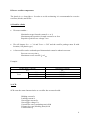
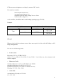
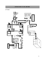
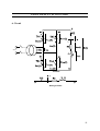
USER’S MANUAL SINGLE-PHASE / DIRECT CURRENT CONVERSION TEST BENCH REF. CO-1000 SINGLEPHASE AC-to-DC CONVERSION BENCH CO-1000 a _ TABLE OF CONTENTS PREAMBLE……………………………………………………………...……………………. 3 INTRODUCTION………………………..………………………….…………...….………… 4 SETTINGS……...……………………………………………………..……………………….. 5 TECHNICAL SPECIFICATIONS………………………………………………….………... 6 I SECURITY, ENVIRONMENT AND EMC……………………....………………..... 6 II ELECTRICAL CHARACTERISTICS…………………………………………...…. 7 III INSTRUCTIONS OF USE AND SECURITY………………….…...…………...… 11 IV FUSES AND POWER COMPONENTS REPLACEMENT………..……………… 12 FEATURES……………………….…………………………..…………….………………..... 14 I LOCATION OF CONTROLS…………………………………………..…………….. II MEASURE AND VIZUALIZATION OF CURRENTS…………….……………..... III REMOVABLE FRONT PANELS. UNCONTROLLED RECTIFICATION.……… IV REMOVABLE FRONT PANELS. CONTROLLED RECTIFICATION……….…. 14 17 19 22 PRACTICAL WORKS : UNCONTROLLED RECTIFICATION………………….…...... 25 I PRELIMINARY SURVEY ON DIODES ASSOCIATION………………………….. II HALF WAVE AND FULL WAVE CENTER TAPPED RECTIFICATION……….. PANEL A – EXP N°1 : RESISTIVE LOAD…………………………………… PANEL A – EXP N°2 : INDUCTIVE LOAD………………………………….. III BRIDGE RECTIFIER DIODE……………………………………………………… PANEL B – EXP N°1 : RESISTIVE LOAD………………………………..….. PANEL B – EXP N°2 : INDUCTIVE LOAD – SMOOTHING INDUCTANCE PANEL B – EXP N°3 : ACTIVE LOAD…………………………………….. PANEL B – EXP N°4 : ACTIVE INDUCTANCE LOAD……..………………. PANEL B – EXP N°5 : DC MOTOR…………………………….………...…... 25 29 32 37 39 40 42 44 48 50 . PRACTICAL WORKS : CONTROLLED RECTIFICATION………………..……...…… 52 I HALF WAVE AND FULL WAVE CENTER TAPPED RECTIFICATION…….….. PANEL C : RESISTIVE LOAD……………………….……….…………...….. II FULL SCRs BRIDGE RECTIFIER.………………………………………….……… PANEL D – EXP N°1 : ACTIVE LOAD..…………………………………...… PANEL D – EXP N°2 : DC MOTOR..………………………….…………..…. III SCRs/DIODES BRIDGE RECTIFIER.……………………………………...……… PANEL D – EXP N°3 : ACTIVE INDUCTANCE LOAD…………………….. PANEL D – EXP N°4 : DC MOTOR…………………………………………... 53 55 58 59 65 66 67 72 2 PREAMBLE With the development of switching components and digital processing, electrotechnics is taking a major place in industrial activities as in electrical engineering, power distribution, transports improvement… Nowadays, power and control electronics appear to have many applications fields and provide for electrotechnics many ambitious prospects. Teachers from technical and professional departments, where practical work must be a priority, are naturally ready to motivate pupils and students to follow electrotechnics studies. The present bench deals with ac-to-dc conversion. 3 INTRODUCTION An ac-to-dc converter supplies dc voltage or dc current to a load from an ac source. An ac-to-dc converter is symbolically pictured as : Electromechanic converters have been replaced by power electronics where switching systems, based on semiconductor components, are more and more efficient. Those systems present many advantages as : low dimensions low cost maintenance free silent high efficiency high flexibility at use 4 SETTINGS This bench presents several originalities so much convenient than educational. It contains all devices required for single phase ac-to-dc conversion, such as rectifiers (diodes) and SCRs and can be used for high school practical works. The bench is used with four removable panels on which clearly appears the following conversion chain: ac source 230 V 50 Hz Transformer Rectifier dc load This bench constitutes a convenient help for the teacher during demonstration lectures and its utilization is strongly recommended for pupils who chose to follow a practical teaching. Rectifier circuits can be chosen by means of four removable panels suited to specific application : ½ Panel A : Full wave center-tapped rectifier ½ Panel B : Bridge rectifier diode ½ Panel C : SCRs full wave center-tapped rectifier ½ Panel D : Bridge rectifier (SCRs or SCRs/diodes) A single bench with its four panels allows to study all kind of ac-to-dc conversions (singlephase) and with the same case, the teacher will choose the corresponding panel to each practical work. An immediate comparison between controlled and uncontrolled components is available by means of switch which commutes a SCR into a diode. This may introduce motor speedvariation. For active inductance load, rectifier or wave generator mode is displayed by two indicators. Rectifier mode : the load is supplied by mains Wave-generator mode : the load (added to a generator) supplies mains 5 TECHNICAL SPECIFICATIONS ! I SECURITY, ENVIRONMENT AND EMC A Security This bench uses secured connections however it is recommended to use a high differential circuit-breaker (30 mA). The socket power unit must be grounded (CLASS 1 case) Primary and secondary windings (power supply transformer) are respectively protected by two fast fuses (4 A and 6.3 A). Electronic stage is protected by a 500 mA fuse Warning Refer servicing to qualified personnel only B Environment Use: +10 °C to 40°C Storage: 0°C to 50°C C EMC This bench complies with European EMC rules; Mains interference, output terminals interferences, radiated interferences, mains harmonic 6 II ELECTRICAL CHARACTERISTICS This device complies with secured voltages : Less than 50 V rms (ac) Less than 120 V (dc) A Power supply Transformer : apparent power S = 200 VA 1) Full wave center-tapped rectifier power supply Power supply : 2 × 15 V rms V (t) = 15 2 sin ωt 1 V (t) = 15 2 sin ωt 2 2) Bridge circuit power supply According to dc load one winding only V1 (t) = 15 2 sin ωt full winding V (t) = 30 2 sin ωt 2 7 B Power rectifier components The bench is a « closed-box ». In order to avoid overheating it is recommended to oversize rectifiers (diodes) and SCRs. 1) Rectifier (diode) We must consider : Maximal average forward current IFAV or Io Maximum peak repetitive forward current IFM or IFRM Repetitive peak inverse voltage VRRM We will impose IFAV >> 3A and VRRM >> 50V and the rectifier package must fit with location (194 plastic type ). A fast rectifier can be used and speed characteristics must be taken in account : Reverse recovery time trr Maximum reverse current IR or IRM Example : POWER RECTIFIER IFAV 200 VRRM 400 600 194 Plastic Package 6A MR 752 MR 754 MR 756 2) SCR SCR owns the same characteristics as a rectifier but we must be add : Holding current IH Latching current IL Gate trigger current IGT Gate trigger voltage VGT Current slew rate (conducting state) di/dt Voltage slew rate (blocking state) dv/dt Turn off time tq 8 SCRs are protected against overvoltage by means of RC circuit. We must also consider : Rms on-state current ITRMS Average forward current ITAV Repetitive peak off-state voltage VDRM or VRRM Peak on-state voltage VTM As for rectifiers, fast SCRs can be used looking at package type (TO 220) Example : POWER SCR ITRMS 200 VDRM 400 PLASTIC PACKAGE TO 220 AB 8A 12A MCR 72-4 2N 6396 TIC 126 B MCR 72-6 2N 6397 TIC 126 D C Load Whatever the load, the maximum current Imax must equal 6A either with half bridge or full bridge arrangements. We can use the following loads : Load resistor Rheostat ref. ECO ½ TUBE (320 W) (10 Ω ; 5.7 A) ; (15Ω ; 4.5 A) (22 Ω ; 3.8 A) (33 Ω ; 3.1 A) for best use, low resistance load must be adopted. Inductance loads Variable inductance 0.1 H to 1.4 H/10Ω/2A ref. PSYJR Smoothing inductance 20 mH/3A ref. CO-105 Dismantle transformer coils (with or without iron core) Winding :125 ; 250 ; 500 ; 1000. Active load Accumulator cell (lead) ref. CO-106 6V ; 12V ; 24V 9 DC motor ref. SH 90/24 Armature supply 24V/6.4 A Inductor supply 24V/0.62 A Speed detector 200Hz-5VAC-1000 rpm Magnetic brake ref. FR 90 Braking voltage 0-10 V (DC) Current 0-60 mA The previous devices are just given as examples and other kind of loads could be used provided that electrical characteristics of the bench are respected. D Current probe, LEM LEM probe is based on Hall effect. It is made of a primary stage (high current) plugged within the circuit (CURRENT PROBE) and the secondary stage is plugged to a scope (BNC socket). Galvanic insulation is made between both stages. This probe can measure ac, dc and TRMS currents. The maximum current must be 6A and the probe sensitivity is 0.5V/A. E Angle of lag ; control and display 1) Trigger Triggering is synchronized with mains and a pulse transformer provides a galvanic insulation. 2) Angle of lag This tuning is realized by means of a potentiometer. Two different modes are available : Rectifier mode : 0 ≤ α ≤ 180° Wave generator mode : 100° ≤ α ≤ 170° The beginning of conduction is obtained with rectifier (diode) for α = 0°. 10 3) Angle of lag ; external control The angle of lag can be controlled by an external dc voltage : 0 ≤ Vext ≤ 12V for 0 ≤ α ≤ 180° 4) Angle of lag display Its measure can be obtained either from the LCD display of the bench or from a scope screen. 5) Pulse chains Two channels First channel : 20 kHz pulse chains applied to G1 and G2, range [α ; 180°] Second channel : 20 kHz pulse chains applied to G3 and G4, range [180° + α ; 360°] III INSTRUCTIONS OF USE AND SECURITY The user should scrupulously respect for his own security and the one of the bench the main following recommendations: 1) Look after the different devices such as seers, emergency stops, meters, scope…at the beginning and at the end of each practical work session. 2) Work out an operative method before every manipulation. 3) The yellow and green coloured earth terminal of the module must be connected by means of earth wire (same colour) to the power supply desk and to the loads that are endowed with. 4) Use secured ∅ 4 mm wires only. 5) To avoid electrical shock, any intervention must be done after disconnecting the ac power cord. 6) Once the circuit is checked by the teacher, this latter will switch on the desk power supply. 7)Do not overpass the maximum ratings of power components and loads. 8) In order to measure and visualise current, do not plug nor disconnect cords of the buckle if current has not been cut-off. 11 WARNING: The bench is a class 1 device, the metallic part of the current probe is grounded. The utilisation of a differential probe is necessary if the measure of the current is not referenced to the mass of the installation. One can use 0.1Ω / 5 W or 1 Ω / 40 W shunts while being careful to connect the mass correctly to one of their terminals. 9) In order to measure and to visualise any tension, connect scope and voltmeter at last. Think about the utilisation of a differential probe if any mass problem is encountered. 10) Use carefully accumulators cell (beware of short circuit). IV FUSES AND POWER COMPONENTS REPLACEMENT No particular maintenance is required for this bench. However install it in a dry place and avoid any inclined position. WARNING : Unplug the module from the power source before replacing any fuse or damaged component (beware of active loads). A Fuses replacement WARNING : Any fuse replacement must be done with a fuse which presents the same characteristics (type, size,) 1) Power stage Fuses are placed on the rear panel in fuse holders. Primary winding (mains) : One 4 A / 250 Vpp /5 × 20 mm fast fuse Secondary winding : Two 6.3 A / 250 Vpp / 5 × 20 mm fast fuses 2) Electronic stage Electronic stage is protected by fuse holder soldered on printed-circuit. 12 Primary winding (mains) : One 500 mA / 250 Vpp /5 * 20 mm temporized fuse B Power components replacement WARNING : If one or some components are damaged, it is recommended to check the others devices even if they seem undamaged. Power components can be unscrewed from the protective panel (transparent cover). 1) SCR replacement After finding the SCR location, unscrew the damaged SCR, place the new one (place a tested SCR). Verify the SCR terminals are well screwed before a new experiment. 2) Rectifier replacement Adjust its terminals. Unscrew the damaged rectifier, place the new one (the central screw is not used, use a tested diode). Before using, verify that the tension is 15 V rms across both windings transformer (while connection straps are removed and no load is connected). Warning: Check the load is not shorted. 13 FEATURES I LOCATION OF CONTROLS AC-DC CONVERSION CURRENT PROBE BRIDGE RECTIFIER RECTIFIER WAVE MAINS 230 V / 50 ANGLE OF DELAY ANGLE CONTROL POWER COMPONENTS POWER STAGE LOAD 14 (1) Title of the circuit (2) Power switch (3) Power supply indicator (4) Rectifier or Wave generator selector (for controlled rectifiers only) (5) Current probe terminals. Imax = 6 A (6) Coaxial output for the current probe(to scope), 0.5 V/A (7) Angle of lag display while control (8) is turned on. (8) Angle of lag control Rectifier mode : 0° ≤ α ≤ 180° Wave generator mode : 100° ≤ α ≤ 170° (9) First half winding of the source transformer indicator (orange). (10) Second half winding of the source transformer indicator (orange) (11) Rectifier or SCR selector : Left position ;Th1 on , D1 off right position ;Th1 off, D1 on (12) Rectifier or SCR selector : Left position ;Th2 on , D2 off Right position ;Th2 off, D2 on (13) Rectifier or SCR selector : Left position ;Th3 on , D3 off Right position ;Th3 off, D3 on (14) Rectifier or SCR selector : Left position ;Th4 on , D4 off Right position ;Th4 off, D4 on (15) Th1 indicator (red) when (11) is on left position (16) BNC socket output for G1 gate signal (same as G3) of Th1. 20 kHz, [α ;π°] range pulses chain. (17) D1 indicator (green) when (11) is on right position 15 (18) Th2 indicator (red) when (12) is on left position (19) BNC socket output for G2 gate signal (same as G3) of Th2. 20 kHz, [π + α ; 2π°] range pulses chain (20) D2 indicator (green) when (12) is on right position (21) T3 indicator (red) when (13) is on left position (22) D3 indicator (green) when (13) is on right position (23) T4 indicator (red) when (14) is on left position (24) D4 indicator (green) when (14) is on right position (25) Connection strap ; V1(t) to circuit (26) Connection strap ; V2 (t) to circuit (27) Connection strap ; link between rectifier devices (1) and (4). First half of the bridge circuit. (28) Connection strap ; link between rectifier devices (2) and (3). Second half of the bridge circuit. (29) Connection strap ; 15 V power supply (30) Load connections, full wave center-tapped rectifier mode (31) Load connections, bridge rectifier mode (32) Rectifier indicator (green), bridge rectifier mode (33) Wave generator indicator (red), bridge rectifier mode (34) Power components (Rectifiers, SCRs) First row : (Th1, Th2, Th3, Th4) Second row : (D1, D2, D3, D4) 16 II MEASURE AND VISUALIZATION OF CURRENTS Every currents can be visualized or measured by means of the different connection straps positions : 17 18 III REMOVABLE FRONT PANELS. UNCONTROLLED RECTIFICATION PANEL A : FULL WAVE CENTER-TAPPED RECTIFIER (TWO DIODES) PANEL B : BRIDGE RECTIFIER DIODE 19 SINGLE PHASE AC-DC CONVERSION probe Current probe UNCONTROLLED RECTIFICATION MAINS OFF LOAD Imax 6 A FULL WAVE CENTER TAPPED RECTIFIER (TWO DIODES) PANNEL A 20 OFF PROBE CURRENT PROBE BRIDGE RECTIFIER DIODE SINGLE PHASE AC-DC CONVESRSION MAINS PANNEL B LOAD Imax 6A 21 IV REMOVABLE FRONT PANELS. CONTROLLED RECTIFICATION PANEL C : SCRs CENTER-TAPPED RECTIFIER (TWO SCRs) PANEL D : BRIDGE RECTIFIER (FULL SCRs OR SCRs AND DIODES) 22 WAVE GENERATOR RECTIFIER PROBE CURRENT PROBE SINGLE PHASE AC-DC CONVERSION MAINS ANGLE OD DELAY ANGLE LOAD SCRs CENTER TAPPED RECTIFIER (TWO SCRs) PANNEL C 23 BRIDGE RECTIFIER RECTIFIER WAVE GENERATOR PROBE SINGLE PHASE AC-DC CONVERSION MAINS ANGLE OF DELAY ANGLE CONTROL PANNEL D LOAD Imax 6A 24 PRACTICAL WORKS : UNCONTROLLED RECTIFICATION I PRELIMINARY SURVEY ON DIODES ASSOCIATION The aim of this survey is to introduce uncontrolled components as diodes (rectifiers). The following applications need dc power supply. A Cathode biasing DL1 : green LED DL2 : red LED VA1, VA2 : DC power supply (0 – 30 V) R : 1 kΩ / ¼ W resistance ½ Circuit : 25 Let’s fill the following table : VA1 VA2 VA1>VA2 +15 V +10 V VA1<VA2 +10 V +15 V UA DL1 DL2 UR First result: When cathodes of these 2 diodes are biased eachother, the conducting diode is the one whose anode’s potential is superior to the anode’s potential of the other diode. This result will be generalized (specially with three-phase rectifier circuits) by comparison of anode’s potential. If VDL1 << VA1 and VDL2 << VA2 then a diode can be considered as a switch (ideal component) and its threshold voltage will be neglected. Therefore we can picture a diode as an one-way switch : Conduction state ( closed switch): VD = 0 V Blocking state(open switch): iD = 0 A This hypothesis will be justified when we use the bench. Second result: For a common cathodes association we notice that the conducting diode forces its anode’s potential to the cathode of the other diode. This result could be generalized to. These results will be seen again with center-tapped circuit. 26 B Anodes biasing DL3 : green LED DL4 : red LED VK3, VK4 : DC power supply (0 – 30 V) R : 1 kΩ / ¼ W resistor ½ Circuit : Let’s fill the following table : VK3 VK4 VK3<VK4 -15 V -10 V VK3>VK4 -10 V -15 V UK DL3 DL4 UR First result: When anodes of these 2 diodes are biased eachother, the conducting diode is the one whose cathode’s potential is inferior to the cathode’s potential of the other diode. 27 Second result: For a common anodes association we notice that the conducting diode forces its cathode’s potential to the anode of the other diode. As the previous survey, these results can be generalized. C Bridge rectifier diode DL1 : green LED DL3 : green LED DL4 : red LED DL2 : red LED U : DC variable power supply (0 – 30 V) R : 1 kΩ / ¼ W resistance Circuit : 28 ½ U > 0 and U < 0 - note the state of diodes measure the potential in A then in B with respect to P or N. explain the behavior of the circuit after the two previously filled tables. justify the fact that: The conduction of a diode involves the other to be in blocking state Remarks: These results suppose that a load is connected. Diodes, transformer are supposed idealized and encroachment is ignored. This confirms the representation of diodes by ideal switches. II HALF WAVE AND FULL WAVE CENTER TAPPED RECTIFICATION Both applications remind the operative mode of diode in power electronics and underline the fact that it behaves in ac-to-dc conversion as a commutating switch. Half wave survey is available by means of center-tapped circuit. The load is placed between the middle point of the transformer winding (M) and both cathodes (S) of D1 and D2. Each transformer winding is connected by connection straps to the anode of each diode. We can use only one connection strap in order to realized a half wave rectifier see fig1.a. and fig1.b. LOAD MAINS Fig.1.a 29 ½ Half wave rectification Fig1.b Full wave rectification is obtained when two connection straps are used simultaneously, see fig1.c. ½ Full wave rectification Fig1.c 30 It would be better to use an analog scope with the following characteristics : memory function vertical sensibility : 10V / div – 20V / div « INV » mode for both channels Source triggering and chopped mode are suitable A digital scope makes the visualization of 50 kHz signals much easier than an analog scope. Moreover it allows mathematics operations as average, sum, Fourier transform…and cursors may be suitable to check conduction interval times. 31 PANEL A EXP N°1 : RESISTIVE LOAD A Circuit diagram LOAD :10 Ω/5.7 A (320 W) or 15 Ω/4.5 A (320 W) Rheostat, Rh ½ Half wave and full wave rectification Two arrangements are used : 32 No connection straps B Tensions waveforms ½ Half wave rectification 1 Visualize V1(t) on channel 1 (ground potential is M point) Explain why the tops of the sine wave are flat ^ Give the maximum value V1 of V1(t) Place the load between S and M points. Use C1 connection strap only. 2 Keep V1(t) on channel 1 and visualize UC(t) on channel 2. ^ Give the maximum value U C of UC(t). 3 Keep these settings and use « INV » and « ADD » functions in order to visualize VD1(t). ^ Give the maximum value V of VD1(t). Remove C1 place C2 4 Visualize V2(t) on channel 1 and UC (t) on channel 2 Give the maximum value V2 of V2(t) Compare V1(t) to V2(t) and V1 with ^ V2 5. Keep these settings, and repeat 3 in order to visualize VD2(t). ^ Give the maximum value V D 2 of VD2(t) 33 ½ Full wave rectification Both connection straps 1 Sketch UC(t) and measure its frequency. 2 Visualize UC(t) after removing and placing again successively C1 and C2. 3 Both straps are placed, sketch VD1(t), VD2(t) below UC(t) and give their maximum values. C Currents wave forms ½ Single wave rectification C1 only 1 Visualize and picture iD1 (t) and iC(t) below V1(t) graph. C2 only 2 Visualize and picture iD2 (t) and iC(t) below V2(t) graph. ½ Full wave rectification Both straps are placed 1 What about iD1(t) and iD2(t) ? 2 Sketch iC(t) below V1(t), V2(t) and UC(t). 34 D Operating analysis ½ Half wave rectification After voltages waveforms explain the action of the circuit. 1 Show that the diode behaves as a switch and verify the following expressions : V1(t) = UC(t) + VD1 (t) (C1 only) V2(t) = UC(t) + VD2(t) (C2 only) 2 Give a conclusion about diodes threshold voltage and the secondary winding of the transformer (supposed ideal). Remark : State under each waveform the name of the conducting diode. 3 After the waveforms of currents, justify the behavior of each diode 4 Compare the current passing through the load and the one passing through the diode. ½ Full Wave rectification After voltages waveforms explain the action of the circuit. 1 Describe briefly half wave rectification compared to full wave rectification and deal with UC(t). 2 Compare diodes maximum inverse voltage (value and shape) 3 Explain why superposition method is not available in these conditions. 4 After currents waveforms, justify the state of each diode and verify the following expression : iC(t) = iD1(t) + iD2(t) 5 Show that iC(t) is a one-way current ; from S to M. 6 After waveforms give a conclusion about this converter. 35 E Remarkable values 1 Compare your results with the following table : ^ UC AC + DC ^ LOAD UC HALF WAVE RECTIFICATION ^ ^ ^ ^ V V 2 V π V Rh FULL WAVE RECTIFICATION ^ ^ ^ ^ V V 2 2V π V Rh __ UC DC IC IC __ IC ^ ^ IC 2 IC π ^ ^ 2 IC π IC 2 How to measure the ac part UCA of UC(t) ? __ What about UC and U C ? 2 Fill the following table DIODE ^ U Drev ^ ID ID __ ID HALF WAVE RECTIFICATION FULL WAVE RECTIFICATION 36 PANEL A EXP N°2 INDUCTANCE LOAD A Circuit LOAD: 10 Ω/5.7 A (320 W) or 15 Ω/4.5 A (320 W) rheostat, Rh and coil with its iron core ½ Half wave rectification C1 and C2 are placed • We use a 0.1 H to 1.4 H variable inductance, with an internal resistor r = 10 Ω 1 Picture the circuit. 2 From the previous survey (resistive load), what changes are encountered towards iD1(t), iD2(t) and iC(t) ? Justify the expression « continuous conduction ». What about the inductance towards the shape of UC(t) ? 3 If L = L1 = 0.1 H ; L = L2 = 0.5 H ; L = L3 = 1.2 H sketch Uc(t) and iC(t). Verify UC(t) = Urh (t) + UL(t) when L = 1.2 H. __ Why U L ≠ 0 ? __ Give the theoretical expression of U C __ 4 Note that I C remains unchanged whatever L value (DC mode). Measure this value and compare it with its theoretical expression : ^ 2V IC = πR T __ Where RT = r + Rh 5 A free wheeling diode Dr is placed in parallel with the load. Show that Dr has no action. 37 6 The current wave ratio is given by τ. τ= I Ca __ IC Where Ica is the rms part of iC(t). How does τ behave compare to L ? Give a conclusion about the function of the inductance Make a comparison between L/RT ant T/2 for L ranging from 0.1 H to 1.4 H. Plot τ = f(L). ^ Confirm these results if we consider : 4 V . I Ca = 2 3π R T + (2Lω) 2 (first harmonic approximation) Work out τ without L. Compare τ values respectively to L values and show that τ≈ 1 RT . when RT<< 2Lω 3 2 Lω ½ Half wave rectification Remove C2 • We chose L = L1 = 0.13 H 1 Visualize and deal about conduction conditions. Sketch UC(t) and iC(t). Explain why UC (t) is not a half wave tension. Explain iC(t) waveform 2 Place in parallel with the load a free wheeling diode Dr. Explain why UC(t) is a half wave tension. Explain iC(t) wave form, what happens while L is increasing ? Deal with the free wheeling diode. 38 III BRIDGE RECTIFIER DIODE. Full wave rectification is reached with center-tapped transformer. Very used for symmetric dc power supply, it is not very suitable for high-voltage applications. In this second case, a bridge rectifier diode is used. The transformer is not a center-tapped on and it is smaller than the previous one. On the inverse cycle, each diode has only transformer voltage across its terminals. Bridge rectifier circuit : (11), (12), (13) and (14) are in right position (diode mode) 39 PANEL B EXP N°1 RESISTIVE LOAD LOAD : 10 Ω / 5.7 A (320 W) or 15 Ω / 4.5 A (320 W) Rheostat, Rh 1 Picture the circuit. 2 Sketch V(t) and UC(t) How to visualize simultaneously both signals ? 3 Sketch VD1(t), VD2(t), VD3(t) and VD4(t) voltage across each diode. Sketch iD1(t), iD2(t), iD3(t) and iD4(t) current in each diode. Sketch the transformer output current iS(t) and the load current iC(t). 4 Explain the action of the circuit (the diode is idealised). Verify instantaneous relations of voltage and current. State the name of conducting diodes. __ __ 5 Measure U C and I C and verify Ohm’s law across the load. __ __ 6 We notice wave phenomenon with U C and I C . let’s introduce : τ = wave ratio F = shape factor Fill the following table : __ UC DC Practical results Theoretical results UCa AC ^ 2V π UC AC+DC __ 2 UC − UC 2 ^ V 2 τ= U Ca __ UC 0.48 F= 1 τ 1.11 __ U C is average value of UC(t) Uca is the rms value of the ac part of UC(t) Uc is the rms value of UC(t) 40 Deal with these results What about τ and F ? We would measure the rms value V of V(t) with a magnetoelectric meter (dc mode only). __ Show that across the load, U C ≈ V 7 Which passive component could enhance this wave phenomenon ? 41 PANEL B EXP N°2 INDUCTANCE LOAD- SMOOTHING INDUCTANCE In power electronics, currents are often waving and that may trouble loads. Losses may appear with dc-motors for example. Therefore we place a high value inductance, called smoothing inductance, in series with the load. That make the current to become rather constant. This experiment deals with the function of a smoothing inductance in series with a resistive load Rh. LOAD : Resistor Rh and a variable inductance L (ref. PSYJR) 1 Draw the circuit. We chose L = 1.2 H 2 Visualize and sketch V(t) and UC(t). Sketch VD1(t), VD2(t), VD3(t) and VD4(t) voltage across each diode. Sketch iD1(t), iD2(t), iD3(t) and iD4(t) current in each diode. Sketch the transformer output current iS(t) and the load current iC(t). Explain the function of the inductance and specify the condition of conduction. Compare these signal shapes with the previous experiment (resistive load). What about the inductance and the shape of UC(t) ? Verify the following expression : UC(t) = Urh(t) + UL(t) ^ ^ 3 Compare U C with V ^ 2V Measure U C and compare with its theoretical value : π __ __ __ Measure I C and verify this value from the relationship between U C and RT (RT = r + Rh) 4. Power: As diodes are idealized no losses appear between the secondary of the transformer and the load. __ __ We assume that : PS = Pload = U C I C 42 Measure PS and Pload with a wattmeter (upstream and downstream arrangements). We assume that S = V IS even if IS is not a sine wave. __ ^ __ Show that IS = I C and write S as a function of V and I C Calculate the power factor k = P S Compare k with 0.9 (theoretical value). Deal with its high value. Find this result with a phaseshift method. 6 Disrupting conduction Replace the previous inductance by a dismantle transformer coil with and without iron core : L1 = 125 windings L2 = 250 L3 = 500 L4 = 1000 Deal with UC(t) and IC(t). Deal with every waveforms and notice how conduction times are changed. 43 PANEL B EXP N°3 ACTIVE LOAD Battery behaves as dc load and can be considered as an ideal dc voltage generator in series with a resistor. Such load does not need any smoothing inductance. A circuit LOAD : 10 Ω/5.7 A (320 W) or 15 Ω/4.5 A (320 W) Rheostat, Rh (ref. ECO ½)and a 6V or 12 V battery (ref. CO-106) Mains 44 B Action of the circuit ½ Tensions waveforms 1 Sketch V(t) and UC(t) separately or use a differential probe in order to visualize both signals. Sketch URh(t) and E. 2 Visualize VD1(t) and VD4(t). 3 Visualize VD2(t) and VD3(t). ½ Currents waveforms 1 After URh(t) graph, sketch iC(t). 2 With the current probe visualize iD1(t), iD2(t), iD3(t) and iD4(t). 3 Visualize the transformer secondary output current iS(t). C Action analysis ½ First half of cycle 1 Specify the considered interval and the sign of V(t). 2 Give any instantaneous relation between UC(t), iC(t), Rh and E. 3 When V(t) ≤ E, show that no current passes through the load and verify that UC(t) = E. Verify that all diodes are in off state. 4 When V(t) > E, state the conducting diodes. Give their repetitive peak inverse voltage Measure the on state interval of the conducting diodes, ∆τ. Derive the following expression : i C (t) = V 2 E sin ωt − Rh Rh 45 From this equation, specify ∆τ. Verify that ∆τ is centred on T/4. ½ Second half of cycle 1 Specify the coincided interval and the sign of V(t). 2 Same survey as before. Derive the following expression : i C (t) = − V 2 E sin ωt − Rh Rh ½ Full cycle 1 Verify that iC(t) is a unidirectional current and the conduction is not continuous. 2 Deal with iS(t) (waveform). What is the action of the bridge towards the battery ? 3 Note the characteristics of the battery. __ Calculate the time τCh needed to load the battery under I C current condition. How can we regulate the load current ?. D remarkable values ½ Average currents Assuming : __ IC = 2 2V 1 cos ωt1 − Rh ∆τ T sin ωt1 46 Where T = 20 ms __ Measure I C and compare it with the previous equation. __ __ Show that I D = = IC 2 _2 Measure IC and find the alternative part I Ca = I C2 − I C and find the wave ratio Ω = I Ca __ IC ½ Average voltage across the load __ __ __ Measure U C and compare with U C = E + R I C ½ Power Measure the incoming power PT at the load. __ Calculate PU = E I c Deduce losses : PJ = PT-PU Determine the efficiency η = Pu PT Measure the apparent power at the output of the transformer and compare with S = V IS = V IC Calculate the power factor k = PT S 47 PANEL B EXP N°4 ACTIVE INDUCTANCE LOAD A Circuit LOAD : From the previous experiment, let add in series with the load a variable inductance. Mains 48 ½ Continuous conduction 1State the changes about iD1(t), iD2(t), iD3(t), iD4(t) and the voltage across the load. 2 Sketch UC(t) and iC(t). 3 Fill the following table. L (H) E 0.13 0.4 0.6 0.8 1 1.2 __ U Rh __ UL __ UC __ IC __ __ __ Verify : U C = U L + U Rh + E __ Why U L ≠ 0 ? Measure RT = Rh + r +rb where Rh is the load resistance, r, the battery internal resistor, r = E Ch − E 0 __ IC __ rb, inductance internal resistor, rb = UL __ IC ½ Disrupted conduction Replace the previous inductance by a 20 mH inductance or dismantle transformer coil. What about UC(t) and iC(t) ? 49 PANEL B EXP N°5 DC MOTOR A Circuit Mains Current probe BRIDGE RECTIFIER WAVE RECTIFIER Probe Current probe Brake SCOPE DC Motor DC Supply 50 LOAD : In a first time a 20 mH inductance is used (ref. CO-105) and in a second time a variable inductance is used. Both are placed in series with a dc motor (ref. SH 90/24). 4 Supply the inductor of the motor then its armature Visualize and deal with Uc(t) waveform. What about the different steps? Notice the motor speed. 5 Visualize ic(t) through the motor and explain why the conduction is disrupted. What about the different peaks? 6 Connect a 20 mH smoothing inductance. What about uc(t) and ic(t) waveforms? What about the conduction mode? Visualize and deal with Uc(t) and ic(t). 7 Replace the previous inductance by a variable inductance (ref. PSYJR). Specify the conduction mode and deal with Uc(t) and IC(t). Why does motor speed decrease? ½ We chose L = 0.1 H Visualize and deal with Uc(t) and IC(t). __ Measure and deal with UC . __ Measure and deal with IC . Calculate the internal resistor of the variable inductance. __ __ __ __ Measure U M and verify U C = U M + U L . __ Compare U C with its theoretical expression. Can the speed motor be modified?. After the previous results, give a method to determine the armature resistor and the speed factor (k). 51 PRACTICAL WORKS: CONTROLLED RECTIFICATION The aim of these practical works is to introduce the SCR. This component is a controlled switch. When its gate is correctly biased, a SCR is in conducting state. It remains in this state as long as the current through it becomes nil or a reverse voltage is applied to it. With a SCR we can obtain a constant tuneable voltage across the load. This is very useful in servings applications, when motor speed must be adjusted. An other application is the wave generator which action is to get back power from the load during braking intervals. (subway). 52 I HALF WAVE AND FULL WAVE CENTER TAPPED RECTIFICATION ½ Half wave rectification Connection straps separately used Half wave rectification can be studied with either C1 connection strap (fig 1.a) or C2 connection strap (fig 1.b). Fig 1.a Fig 1.b 53 ½ Full wave rectification (fig 1.c) Both connection straps Fig 1.c Remarks : 1) The angle of lag, α, is calculated after the diodes conduction times (natural switching) 2) Previous results will be seen again and applied to SCRs. This allows to make an easy comparison between controlled and uncontrolled components. First result: When cathodes of 2 SCRs are biased eachother, the conducting SCR is the one whose anode’s potential is superior to the anode’s potential of the other SCR. The conducting SCR forces its anode’s potential to the cathode of the other SCR. Second result: When anodes of 2 SCRs are biased eachother, the conducting SCR is the one whose cathodes’s potential is inferior to the cathode’s potential of the other SCR. The conducting SCR forces its cathode’s potential to the anode of the other SCR. Third result: The on-state of a SCR involves the other SCR to be in the off state. 54 PANEL C RESISTIVE LOAD A SCRs control 1 When α = 30 ° and α = 120°, visualize the gate signal of Th1 on channel 1 and the gate signal of Th2 on channel 2 (respectively named G1 and G2, BNC socket). Compare the scope display with the bench LCD display. 2 Give the conducting dates of Th1 and Th2 when α changes from 0° to 180°. What about the pulses chain ? What is the main advantage of such control ? Measure the frequency of these pulses. B Circuits LOAD : 10 Ω/5.7 A (320 W) or 15 Ω/4.5 A (320 W) rheostat, Rh ½ Half wave controlled rectification C1 connection strap only 1 Visualize V1(t) on channel 1 and UC(t) on channel 2. What about UC(t) towards α variations. ? When α = 60 °, sketch V1(t), UC(t) and G1. 2 Keep these settings and use « INV » and « ADD » functions in order to visualize VTH1(t). Verify the following expression : V1(t) = UC(t) + VTH1(t) 3 Commute (11) while α is tuned. 55 Compare UC with Uc in non controlled rectification. Explain why a SCR is often called « controlled diode ». 4 Explain briefly the action of the circuit and notice when Th1 is in the on state. Remove C1 and place C2 5 Visualize V2(t) on channel 1 and UC(t) on channel 2. What about UC(t) towards α variations. ? When α = 60 °, sketch V2(t), UC(t) and G2. 6 Keep these settings and use « INV » and « ADD » functions in order to visualize VTH2(t). Verify the following expression : V2(t) = UC(t) + VTH2(t) 7 Compare this circuit with the previous one. 8 Explain briefly the action of the circuit and notice when Th2 is in the on state. ½ Full wave rectification C1 and C2 used (α = 60°) 1 Visualize UC(t) after removing and placing again successively C1 and C2. 2 Commute (11) and (12) and notice uncontrolled rectification. 3 Explain the action of this circuit. 4 What about α = 0° and α = 180° ? 5 Show that iC(t) is unidirectional current (from S to M). 56 C Remarkable values 1 Fill the following table : α 0 30° 60° 90° 120° 150° 180° __ UC practical __ UC theoretical __ IC practical __ IC theoretical __ 2 Plot U C = f (α) Point out the uncontrolled rectification. 3 Find these practical results for half wave rectification. Compare these results with full wave rectification results. 57 II FULL SCRs BRIDGE RECTIFIER The four previous diodes are replaced by controlled components. Commute (11), (12), (13) and (14) into SCRs position. 58 PANEL D EXP N°1 ACTIVE LOAD A Circuit Mains Rectifier Wave generator 59 B Rectifier mode LOAD : 10 Ω/5.7 A (320 W) or 15 Ω / 4.5 A (320 W) rheostat, Rh 6 V battery (or 12 V), variable inductance, Lmax = 1.2 H Commute (4) into rectifier mode A SCRs control 1 When α = 30°, visualize G1 on channel 1 and G2 on channel 2. 2 Guess and sketch G3 and G4. ½ Continuous conduction __ __ 1 Place meters for Uc, Ic, U C , I C and P. 2 Verify that the conduction is continuous. The green indicator is on Tune α up to continuous conduction limit. Call αmax this value. 3 Sketch V(t), UC(t), iC(t) and iS(t) when α = 30°. 60 4 Fill the following table : αL α __ Uc practical __ Uc theoretical __ IC practical __ IC theoretical __ P practical __ P theoretical __ __ __ 5 Plot U C = f(α), I C = f(α), P = f(α) __ __ __ 6 Verify after the table : U C = U L + U Rh + E 7 Visualize UL(t) in ac and dc mode. __ What the meaning of U L ? Determine the inductance internal resistor. 8 Measure and calculate RT. RT = Rh + r + rb where Rh is the 10 Ω load resistor, r, the battery internal resistor r = E CH − E 0 __ . IC __ 9 Connect a free wheeling diode Dr in parallel with the load. What about UC(t), and I C ? 10 Power 61 The transformer supplies Ps. ^ __ 2 V __ where U C = I C cosα π __ __ PS = Pload = U C I C The apparent power is given by : ^ __ S= V IC 2 When α = 30° and α = 60°, measure Ps , S and calculate the power factor k. Compare k with 0.9 cos. α. How can we consider α in time scale ? ½ Disrupted conduction 1 Chose α = 30° and remove the inductance Visualize Uc(t) and iC(t). What is the interest of this circuit if the load is a battery ? 2 Replace the previous inductance by a 20 mH one or dismantle transformer coils. What about UC(t) and iC(t). Deal with the flats on Uc(t) waveform. 3 Tune Rh while the disrupted conduction is reached (limit). 62 C Wave generator mode LOAD : 10 Ω / 5.7 A (320 W) or 15 Ω / 4.5 A (320 W) rheostat, Rh 24 V battery (or 12 V), variable inductance, Lmax = 1.2 H Commute (4) into wave generator mode 1 Warning : connect properly the terminals of the battery. ½ Continuous conduction 2 Verify that continuous conduction is reached. The red indicator is on. 3 Sketch V(t), UC(t), iC(t) and iS(t) when α = 120°. 4 Fill the following table : α 100° 105° 110° 115° 120° 125° αL 130° __ Uc practical __ Uc theoretical __ IC practical __ IC theoretical __ P practical __ P theoretical __ __ __ 5 Plot U C = f(α), I C = f(α), P = f(α) 63 __ __ __ 6 Verify after the table : U C = U L + U Rh + E 7 Why does UC(t) sign and not iC(t) makes P to be negative ? Which value for α makes the power from load to source to be maximal ? When α = 120°, how can we tune P ? Tune the circuit in order to reach P = 5W 8 What about power sign according to rectifier or wave generator mode ? What about the source voltage frequency and the voltage frequency across the load ? ½ Disrupted conduction 1 Chose α = 30° and remove the inductance. Visualize UC(t) and iC(t). 64 PANEL D EXP N°2 DC MOTOR LOAD : 0.1 H to 1.4 H variable inductance (ref. PSYJR) or a 20 mH inductance (ref. CO105) in series with a dc-motor (ref. SH 90/24) 1 Supply first the inductor of the motor then its armature. 2 Visualize UC(t) across the motor terminals. How does the motor behave when α is increasing from zero ? 3 Visualize iC(t) and tell why the conduction is disrupted. 4 We place a variable inductance. Tell about the conduction mode and deal with the action of this smoothing inductance. Why does the speed decrease ? L = 0.1 H, continuous conduction Visualize UC(t) and iC(t) Compare these waveforms with the ones obtained in Panel D exp. n°1. __ __ __ Verify U C = U M + U L What do you notice while the inductance is removed ? 5 Place the inductance again and brake gently the motor up to disrupted mode is reached. Replace the previous inductance by lower ones. Visualize UC(t) and iC(t) What about the conduction mode ? Act on α, L or the brake and see how conduction is modified. 6 Fill the following table (continuous conduction, L = 0.1 H). αmax α __ U C practical N speed __ 7 After the table, verify that : __ __ UC = UM + UL __ 8 Plot U C = f (α) and N = f(α) 65 III SCRs/DIODES BRIDGE RECTIFIER This type of circuit can not be used for wave generator applications. It offers the best power factor and its control is more flexible than a full SCRs bridge. Each arm of the bridge contains one SCR and one diode in series. Two arrangements are used : • Symmetrical bridge fig 1 • Non symmetrical bridge fig 2 66 PANEL D EXP N°3 ACTIVE INDUCTANCE LOAD COMPARISON BETWEEN SCRs BRIDGE AND SCRs/DIODES BRIDGE LOAD : 10Ω/5.7 A (320 W) or 15 Ω/4.5 A (320 W) rheostat, Rh ; 6V battery (or 12 V) ; 1.2 H max variable inductance • SYMMETRICAL BRIDGE Fig 1. 67 • NON SYMMETRICAL BRIDGE Fig 2 . Commute (4) in rectifier mode __ __ Place meters for Uc, IC, U C , I C and P. A Preliminary survey : induced load 1 For 0° ≤ α ≤ 180°, change from symmetrical arrangement to non symmetrical. In both cases : Visualize and compare UC(t) and iC(t). Visualize and explain the currents waveforms through each rectifier component. Explain briefly the action of each arrangement. 2 Chose α = 60° in symmetrical arrangement. 68 Using a differential probe, visualize and sketch V(t), UC(t), iTh1(t), iTh2(t), iTh3(t), iTh4(t), iD1(t), iD2(t), iS(t) and iC(t). Explain briefly the action of this circuit. State the name of the conducting components below the gate signals chronograms. 3 Commute (11), (12), (13) and (14) in order to obtain a SCRs bridge. Compare these waveforms with the previous ones. __ __ Tuning α, compare U C and I C while passing from SCRs bridge to SCRs/diodes bridge. B Active inductance load We add a 6V or 12 V accumulators cell. 1 Same questions as before. Make a comparison with the previous results and show that disrupted conduction is reached for a remarkable value of α called αL. 2 Place the load in order to show the reversing function of a SCRs bridge. 3 Fill the following table (SCRs/diodes bridge). α αL __ Uc practical __ Uc theoretical __ IC practical __ IC theoretical __ P practical __ P theoretical 69 __ __ __ Plot U C = f(α), I C = f(α), P = f(α) __ __ __ Verify after the table : U C = U L + U Rh + E Visualize UL(t) in ac and dc mode. __ What about U L ? Determine the inductance internal resistor rb. Measure and calculate RT. RT = Rh + r + rb where Rh is the 10 Ω load resistor, r, the battery internal resistor r = E CH − E 0 __ . IC __ Express I C as a function of V, E, α, Rh and r. So find αL. __ __ What about U C and α if we want I C = 0.7A ? Connect a free wheeling diode Dr in parallel with the load. What about UC(t), and iS(t) ? What about the conduction time interval of each rectifier component ? What is the action of the free wheeling diode ? Power ; we assume the bridge is lossless. The transformer supplies Ps. ^ __ __ PS = Pload = U C I C 2 V __ where U C = I C cosα π __ The apparent power is given by : ^ V __ S= IS 2 Chose α = 30° (continuous conduction) 70 • SCRs bridge rectifier ^ __ __ Measure V, U C and I C . Measure or calculate PS. __ Measure or calculate S (IS = I C ) Calculate k (compare it with 0.9 cos. 30°) • SCRs/diodes bridge rectifier __ __ Tune α for U C = USCRs Show that PSCRs/diodes = PSCRs Work out IS from an area analysis (iS(t) on scope). So find S. • Compare both power factors. 71 PANEL D EXP N°4 DC-MOTOR Same questions as Panel D exp. n°2 and make a comparison with Panel D exp. n°3. 72 CO1000-GB-07-2001