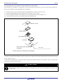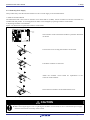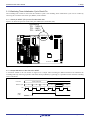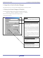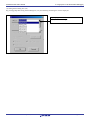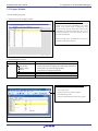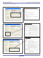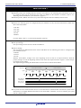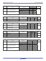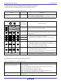
1
To our customers,
Old Company Name in Catalogs and Other Documents
On April 1st, 2010, NEC Electronics Corporation merged with Renesas Technology
Corporation, and Renesas Electronics Corporation took over all the business of both
companies. Therefore, although the old company name remains in this document, it is a valid
Renesas Electronics document. We appreciate your understanding.
Renesas Electronics website: http://www.renesas.com
April 1st, 2010
Renesas Electronics Corporation
Issued by: Renesas Electronics Corporation (http://www.renesas.com)
Send any inquiries to http://www.renesas.com/inquiry.
Notice
1.
2.
3.
4.
5.
6.
7.
All information included in this document is current as of the date this document is issued. Such information, however, is
subject to change without any prior notice. Before purchasing or using any Renesas Electronics products listed herein, please
confirm the latest product information with a Renesas Electronics sales office. Also, please pay regular and careful attention to
additional and different information to be disclosed by Renesas Electronics such as that disclosed through our website.
Renesas Electronics does not assume any liability for infringement of patents, copyrights, or other intellectual property rights
of third parties by or arising from the use of Renesas Electronics products or technical information described in this document.
No license, express, implied or otherwise, is granted hereby under any patents, copyrights or other intellectual property rights
of Renesas Electronics or others.
You should not alter, modify, copy, or otherwise misappropriate any Renesas Electronics product, whether in whole or in part.
Descriptions of circuits, software and other related information in this document are provided only to illustrate the operation of
semiconductor products and application examples. You are fully responsible for the incorporation of these circuits, software,
and information in the design of your equipment. Renesas Electronics assumes no responsibility for any losses incurred by
you or third parties arising from the use of these circuits, software, or information.
When exporting the products or technology described in this document, you should comply with the applicable export control
laws and regulations and follow the procedures required by such laws and regulations. You should not use Renesas
Electronics products or the technology described in this document for any purpose relating to military applications or use by
the military, including but not limited to the development of weapons of mass destruction. Renesas Electronics products and
technology may not be used for or incorporated into any products or systems whose manufacture, use, or sale is prohibited
under any applicable domestic or foreign laws or regulations.
Renesas Electronics has used reasonable care in preparing the information included in this document, but Renesas Electronics
does not warrant that such information is error free. Renesas Electronics assumes no liability whatsoever for any damages
incurred by you resulting from errors in or omissions from the information included herein.
Renesas Electronics products are classified according to the following three quality grades: “Standard”, “High Quality”, and
“Specific”. The recommended applications for each Renesas Electronics product depends on the product’s quality grade, as
indicated below. You must check the quality grade of each Renesas Electronics product before using it in a particular
application. You may not use any Renesas Electronics product for any application categorized as “Specific” without the prior
written consent of Renesas Electronics. Further, you may not use any Renesas Electronics product for any application for
which it is not intended without the prior written consent of Renesas Electronics. Renesas Electronics shall not be in any way
liable for any damages or losses incurred by you or third parties arising from the use of any Renesas Electronics product for an
application categorized as “Specific” or for which the product is not intended where you have failed to obtain the prior written
consent of Renesas Electronics. The quality grade of each Renesas Electronics product is “Standard” unless otherwise
expressly specified in a Renesas Electronics data sheets or data books, etc.
“Standard”:
8.
9.
10.
11.
12.
Computers; office equipment; communications equipment; test and measurement equipment; audio and visual
equipment; home electronic appliances; machine tools; personal electronic equipment; and industrial robots.
“High Quality”: Transportation equipment (automobiles, trains, ships, etc.); traffic control systems; anti-disaster systems; anticrime systems; safety equipment; and medical equipment not specifically designed for life support.
“Specific”:
Aircraft; aerospace equipment; submersible repeaters; nuclear reactor control systems; medical equipment or
systems for life support (e.g. artificial life support devices or systems), surgical implantations, or healthcare
intervention (e.g. excision, etc.), and any other applications or purposes that pose a direct threat to human life.
You should use the Renesas Electronics products described in this document within the range specified by Renesas Electronics,
especially with respect to the maximum rating, operating supply voltage range, movement power voltage range, heat radiation
characteristics, installation and other product characteristics. Renesas Electronics shall have no liability for malfunctions or
damages arising out of the use of Renesas Electronics products beyond such specified ranges.
Although Renesas Electronics endeavors to improve the quality and reliability of its products, semiconductor products have
specific characteristics such as the occurrence of failure at a certain rate and malfunctions under certain use conditions. Further,
Renesas Electronics products are not subject to radiation resistance design. Please be sure to implement safety measures to
guard them against the possibility of physical injury, and injury or damage caused by fire in the event of the failure of a
Renesas Electronics product, such as safety design for hardware and software including but not limited to redundancy, fire
control and malfunction prevention, appropriate treatment for aging degradation or any other appropriate measures. Because
the evaluation of microcomputer software alone is very difficult, please evaluate the safety of the final products or system
manufactured by you.
Please contact a Renesas Electronics sales office for details as to environmental matters such as the environmental
compatibility of each Renesas Electronics product. Please use Renesas Electronics products in compliance with all applicable
laws and regulations that regulate the inclusion or use of controlled substances, including without limitation, the EU RoHS
Directive. Renesas Electronics assumes no liability for damages or losses occurring as a result of your noncompliance with
applicable laws and regulations.
This document may not be reproduced or duplicated, in any form, in whole or in part, without prior written consent of Renesas
Electronics.
Please contact a Renesas Electronics sales office if you have any questions regarding the information contained in this
document or Renesas Electronics products, or if you have any other inquiries.
(Note 1) “Renesas Electronics” as used in this document means Renesas Electronics Corporation and also includes its majorityowned subsidiaries.
(Note 2) “Renesas Electronics product(s)” means any product developed or manufactured by or for Renesas Electronics.
User’s Manual
M34552T2-CPE
User’s Manual
Compact Emulator for 4552, 4553 and 4556
Groups
Rev.4.00 2005.04
Keep safety first in your circuit designs!
1. Renesas Technology Corp. puts the maximum effort into making semiconductor products
better and more reliable, but there is always the possibility that trouble may occur with them.
Trouble with semiconductors may lead to personal injury, fire or property damage.
Remember to give due consideration to safety when making your circuit designs, with appropriate measures such as (i) placement of substitutive, auxiliary circuits, (ii) use of nonflammable material or (iii) prevention against any malfunction or mishap.
Notes regarding these materials
1. These materials are intended as a reference to assist our customers in the selection of the
Renesas Technology Corp. product best suited to the customer's application; they do not
convey any license under any intellectual property rights, or any other rights, belonging to
Renesas Technology Corp. or a third party.
2. Renesas Technology Corp. assumes no responsibility for any damage, or infringement of any
third-party's rights, originating in the use of any product data, diagrams, charts, programs,
algorithms, or circuit application examples contained in these materials.
3. All information contained in these materials, including product data, diagrams, charts, programs and algorithms represents information on products at the time of publication of these
materials, and are subject to change by Renesas Technology Corp. without notice due to
product improvements or other reasons. It is therefore recommended that customers contact
Renesas Technology Corp. or an authorized Renesas Technology Corp. product distributor
for the latest product information before purchasing a product listed herein.
The information described here may contain technical inaccuracies or typographical errors.
Renesas Technology Corp. assumes no responsibility for any damage, liability, or other loss
rising from these inaccuracies or errors.
Please also pay attention to information published by Renesas Technology Corp. by various
means, including the Renesas Technology Corp. Semiconductor home page (http://
www.renesas.com).
4. When using any or all of the information contained in these materials, including product data,
diagrams, charts, programs, and algorithms, please be sure to evaluate all information as a
total system before making a final decision on the applicability of the information and
products. Renesas Technology Corp. assumes no responsibility for any damage, liability or
other loss resulting from the information contained herein.
5. Renesas Technology Corp. semiconductors are not designed or manufactured for use in a
device or system that is used under circumstances in which human life is potentially at stake.
Please contact Renesas Technology Corp. or an authorized Renesas Technology Corp.
product distributor when considering the use of a product contained herein for any specific
purposes, such as apparatus or systems for transportation, vehicular, medical, aerospace,
nuclear, or undersea repeater use.
6. The prior written approval of Renesas Technology Corp. is necessary to reprint or reproduce
in whole or in part these materials.
7. If these products or technologies are subject to the Japanese export control restrictions, they
must be exported under a license from the Japanese government and cannot be imported
into a country other than the approved destination.
Any diversion or reexport contrary to the export control laws and regulations of Japan and/ or
the country of destination is prohibited.
8. Please contact Renesas Technology Corp. for further details on these materials or the
products contained therein.
M34552T2-CPE User’s Manual
Preface
Preface
The M34552T2-CPE is a compact emulator for the 4552, 4553 and 4556 Groups MCUs with the real-time trace function.
This user's manual mainly describes specifications of the M34552T2-CPE compact emulator and how to setup it. For details on
the following products included with the M34552T2-CPE, refer to each product's online manual.
Emulator debugger:
Assembler:
M3T-PD45M
ASM45
All the components of this product are shown in "1.1 Package Components" (page 13). If there is any question or doubt about
this product, contact your local distributor.
The related manuals for using this product are listed below. You can download the latest manuals from the Renesas Tools
homepage (http://www.renesas.com/en/tools).
Related manuals
Item
Emulator debugger
Assembler
REJ10J0130-0400 Rev.4.00
Manual
M3T-PD45M User’s Manual
ASM45 User’s Manual
April 16, 2005
Page 3 of 73
M34552T2-CPE User’s Manual
Important
Important
Before using this product, be sure to read this user’s manual carefully.
Keep this user’s manual, and refer to this when you have questions about this product.
Emulator:
The emulator in this document refers to the following products that are manufactured by Renesas Technology Corp.:
(1) Compact emulator main unit
(2) Package converter board for connecting the user system
The emulator herein does not include the customer’s user system and host machine.
Purpose of use of the emulator:
This emulator is a device to support the development of a system that uses the 4500 Series 4552, 4553 and 4556 Groups of
Renesas 4-bit single-chip MCUs. It provides support for system development in both software and hardware.
Be sure to use this emulator correctly according to said purpose of use. Please avoid using this emulator for other than its
intended purpose of use.
For those who use this emulator:
This emulator can only be used by those who have carefully read this user’s manual and know how to use it.
Use of this emulator requires the basic knowledge of electric circuits, logical circuits, and MCUs.
When using the emulator:
(1) This product is a development supporting unit for use in your program development and evaluation stages. In massproducing your program you have finished developing, be sure to make a judgment on your own risk that it can be put to
practical use by performing integration test, evaluation, or some experiment else.
(2) In no event shall Renesas Solutions Corp. be liable for any consequence arising from the use of this product.
(3) Renesas Solutions Corp. strives to renovate or provide a workaround for product malfunction at some charge or without
charge. However, this does not necessarily mean that Renesas Solutions Corp. guarantees the renovation or the provision
under any circumstances.
(4) This product has been developed by assuming its use for program development and evaluation in laboratories. Therefore,
it does not fall under the application of Electrical Appliance and Material Safety Law and protection against
electromagnetic interference when used in Japan.
(5) Renesas Solutions Corp. cannot predict all possible situations or possible cases of misuse where a potential danger exists.
Therefore, the warnings written in this user’s manual and the warning labels attached to this emulator do not necessarily
cover all of such possible situations or cases. Please be sure to use this emulator correctly and safely on your own
responsibility.
(6) This product is not qualified under UL or other safety standards and IEC or other industry standards. This fact must be
taken into account when taking this product from Japan to some other country.
REJ10J0130-0400 Rev.4.00
April 16, 2005
Page 4 of 73
M34552T2-CPE User’s Manual
Important
Usage restrictions:
This emulator has been developed as a means of supporting system development by users. Therefore, do not use it as a device
used for equipment-embedded applications. Also, do not use it for developing the systems or equipment used for the following
purposes either:
(1) Transportation and vehicular
(2) Medical (equipment where human life is concerned)
(3) Aerospace
(4) Nuclear power control
(5) Undersea repeater
If you are considering the use of this emulator for one of the above purposes, please be sure to consult your local distributor.
About product changes:
We are constantly making efforts to improve the design and performance of this emulator. Therefore, the specification or
design of this emulator or its user’s manual may be changed without prior notice.
About the rights:
(1) We assume no responsibility for any damage or infringement on patent rights or any other rights arising from the use of
any information, products or circuits presented in this user’s manual.
(2) The information or data in this user’s manual does not implicitly or otherwise grant a license for patent rights or any other
rights belonging to us or third parties.
(3) This user’s manual and this emulator are copyrighted, with all rights reserved by us. This user’s manual may not be copied,
duplicated or reproduced, in whole or part, without prior written consent of us.
About diagrams:
The diagrams in this user’s manual may not all represent exactly the actual object.
REJ10J0130-0400 Rev.4.00
April 16, 2005
Page 5 of 73
M34552T2-CPE User’s Manual
Precautions for Safety
Precautions for Safety
Definitions of Signal Words
In both the user’s manual and on the product itself, several icons are used to insure proper handling of this product and also to
prevent injuries to you or other persons, or damage to your properties.
This chapter describes the precautions which should be taken in order to use this product safely and properly. Be sure to read
this chapter before using this product.
This symbol represents a warning about safety. It is used to arouse caution about a potential
danger that will possibly inflict an injury on persons. To avoid a possible injury or death,
please be sure to observe the safety message that follows this symbol.
DANGER
DANGER indicates an imminently dangerous situation that will cause death or heavy wound
unless it is avoided. However, there are no instances of such danger for the product presented
in this user's manual.
WARNING
WARNING indicates a potentially dangerous situation that will cause death or heavy wound
unless it is avoided.
CAUTION
CAUTION indicates a potentially dangerous situation that will cause a slight injury or a
medium-degree injury unless it is avoided.
CAUTION
CAUTION with no safety warning symbols attached indicates a potentially dangerous
situation that will cause property damage unless it is avoided.
IMPORTANT
This is used in operation procedures or explanatory descriptions to convey exceptional
conditions or cautions to the user.
In addition to the five above, the following are also used as appropriate.
means WARNING or CAUTION.
Example:
CAUTION AGAINST AN ELECTRIC SHOCK
means PROHIBITION.
Example:
DISASSEMBLY PROHIBITED
means A FORCIBLE ACTION.
Example:
UNPLUG THE POWER CABLE FROM THE RECEPTACLE.
REJ10J0130-0400 Rev.4.00
April 16, 2005
Page 6 of 73
M34552T2-CPE User’s Manual
Precautions for Safety
WARNING
Warnings for AC Power Supply:
If the attached AC power cable does not fit the receptacle, do not alter the AC power cable and do not plug it
forcibly. Failure to comply may cause electric shock and/or fire.
Use an AC power cable which complies with the safety standard of the country.
Do not touch the plug of the AC power cable when your hands are wet. This may cause electric shock.
This product is connected signal ground with frame ground. If your developing product is transformless (not
having isolation transformer of AC power), this may cause electric shock. Also, this may give an unrepairable
damage to this product and your developing one.
While developing, connect AC power of the product to commercial power through isolation transformer in
order to avoid these dangers.
If other equipment is connected to the same branch circuit, care should be taken not to overload the circuit.
When installing this equipment, insure that a reliable ground connection is maintained.
If you smell a strange odor, hear an unusual sound, or see smoke coming from this product, then disconnect
power immediately by unplugging the AC power cable from the outlet.
Do not use this as it is because of the danger of electric shock and/or fire. In this case, contact your local
distributor.
Before setting up this emulator and connecting it to other devices, turn off power or remove a power cable to
prevent injury or product damage.
Warnings to Be Taken for This Product:
Do not disassemble or modify this product. Personal injury due to electric shock may occur if this product is
disassembled and modified. Disassembling and modifying the product will void your warranty.
Make sure nothing falls into the cooling fan on the top panel, especially liquids, metal objects, or anything
combustible.
Warning for Installation:
Do not set this product in water or areas of high humidity. Make sure that the product does not get wet. Spilling
water or some other liquid into the product may cause unrepairable damage.
Warning for Use Environment:
This equipment is to be used in an environment with a maximum ambient temperature of 35°C. Care should be
taken that this temperature is not exceeded.
REJ10J0130-0400 Rev.4.00
April 16, 2005
Page 7 of 73
M34552T2-CPE User’s Manual
Precautions for Safety
CAUTION
Notes on Connecting the Power Supply of the Emulator:
Do not use any power cable other than the one that is included with the product.
The power cable included with the product has its positive and negative poles color-coded by red and black,
respectively.
Pay attention to the polarities of the power supply. If its positive and negative poles are connected in reverse,
the internal circuit may be broken.
Do not apply any voltages exceeding the product’s rated power supply voltage (5.0 V ±5%). Extreme voltages
may cause a burn due to abnormal heat or cause the internal circuit to break down.
Cautions to Be Taken for Turning On the Power:
Turn ON/OFF the power of the emulator and user system as simultaneously as possible.
Do not leave either the emulator or user system powered on, because of leakage current the internal circuits may
be damaged.
When turning on the power again after shutting off the power, wait about 10 seconds.
Cautions to Be Taken for Handling This Product:
Use caution when handling the main unit. Be careful not to apply a mechanical shock.
Do not touch the connector pins of the emulator main unit and the target MCU connector pins directly. Static
electricity may damage the internal circuits.
Do not pull this emulator by the communications interface cable or the flexible cable for connecting the user
system. And, excessive flexing or force may break conductors.
Caution to Be Taken for System Malfunctions:
If the emulator malfunctions because of interference like external noise, do the following to remedy the trouble.
(1) Press the RESET button on the emulator upper panel.
(2) If normal operation is not restored after step (1), shut OFF the emulator once and then reactivate it.
REJ10J0130-0400 Rev.4.00
April 16, 2005
Page 8 of 73
M34552T2-CPE User’s Manual
Contents
Contents
Page
Preface..........................................................................................................................................................................3
Related manuals ...........................................................................................................................................................3
Important.......................................................................................................................................................................4
Precautions for Safety ..................................................................................................................................................6
Contents........................................................................................................................................................................9
User Registration ........................................................................................................................................................11
Terminology ................................................................................................................................................................12
1. Outline.....................................................................................................................................................................13
1.1 Package Components ..........................................................................................................................................13
1.2 System Configuration ...........................................................................................................................................14
1.2.1 System Configuration ..........................................................................................................................14
1.2.2 Names and Functions of each part of the Emulator............................................................................16
1.3 Specifications........................................................................................................................................................18
1.4 Operating Environment.........................................................................................................................................19
2. Setup.......................................................................................................................................................................20
2.1 Flowchart of Starting Up the Emulator..................................................................................................................20
2.2 Installing the Emulator Debugger .........................................................................................................................21
2.2.1 Installing the Emulator Debugger M3T-PD45M ..................................................................................21
2.2.2 Installing the USB Device Driver .........................................................................................................21
2.3 Connecting the Power Supply for the Emulator....................................................................................................22
2.4 Connecting the Host Machine...............................................................................................................................23
2.5 Turning ON the Power ..........................................................................................................................................24
2.5.1 MCU Power Supply Voltage Selection Switch ....................................................................................24
2.5.2 Checking Connections of the Emulator System..................................................................................25
2.5.3 Turning ON/OFF the Power ................................................................................................................25
2.5.4 Power Supply to the User System ......................................................................................................25
2.5.5 LED Display When the Emulator Starts Up Normally .........................................................................26
2.6 Downloading Firmware .........................................................................................................................................28
2.6.1 When It is Necessary to Download Firmware .....................................................................................28
2.6.2 Downloading Firmware in Maintenance Mode....................................................................................28
2.7 Self-check .............................................................................................................................................................29
2.7.1 Self-check Procedure ..........................................................................................................................29
2.7.2 If an Error is Detected in the Self-check..............................................................................................30
2.8 Connecting the User System ................................................................................................................................31
2.8.1 Connecting to a 2.54-mm-pitch Dual-line Pins....................................................................................32
2.8.2 Connecting to an IC socket for a 48-pin SSOP on the User System..................................................34
2.8.3 Connecting to a 32-pin LQFP foot pattern on the User System .........................................................36
2.9 Changing Settings ................................................................................................................................................37
2.9.1 Changing the Power Supply Voltage to the MCU ...............................................................................37
2.9.2 Port/Segment Output Selection Switches ...........................................................................................38
2.9.3 Port/Subclock Selection Switches.......................................................................................................38
2.9.4 Selecting Clock Supply .......................................................................................................................39
2.10 Connecting the External Trace/Trigger Cable ....................................................................................................41
2.10.1 Connecting the External Trace/Trigger Cable to the Emulator System ............................................41
2.10.2 Connecting the External Trace/Trigger Cable to the User System...................................................41
2.10.3 Specifications of the External Trace/Trigger Cable...........................................................................42
2.11 Watchdog Timer Initialization Cycle Check Pin ..................................................................................................43
2.11.1 Check pin WRST (TP3) on the Emulator Main Unit..........................................................................43
2.11.2 Output Waveform of the Check Pin WRST.......................................................................................43
REJ10J0130-0400 Rev.4.00
April 16, 2005
Page 9 of 73
M34552T2-CPE User’s Manual
Contents
Page
3. Usage (How to Use the Emulator Debugger) .........................................................................................................44
3.1 Starting Up the Emulator Debugger (Init Dialog Box)...........................................................................................44
3.2 Program Window ..................................................................................................................................................46
3.3 Hardware Breakpoint Setting Window..................................................................................................................50
3.4 Trace Window .......................................................................................................................................................52
3.5 Time Measurement...............................................................................................................................................56
4. Hardware Specifications .........................................................................................................................................57
4.1 Target MCU Specifications ...................................................................................................................................57
4.2 Differences between the Actual MCU and Emulator ............................................................................................58
4.3 Connection Diagram .............................................................................................................................................62
4.4 External Dimensions.............................................................................................................................................64
4.4.1 External Dimensions of the Compact Emulator ..................................................................................64
4.5 Notes on Using This Product ................................................................................................................................65
5. Troubleshooting ......................................................................................................................................................67
5.1 Flowchart to Remedy the Troubles.......................................................................................................................67
5.2 When the Emulator Debugger Does Not Start Up Properly .................................................................................68
5.3 How to Request for Support .................................................................................................................................69
6. Maintenance and Guarantee ..................................................................................................................................70
6.1 User Registration ..................................................................................................................................................70
6.2 Maintenance .........................................................................................................................................................70
6.3 Guarantee .............................................................................................................................................................70
6.4 Repair Provisions..................................................................................................................................................70
6.5 How to Make Request for Repair .........................................................................................................................71
REJ10J0130-0400 Rev.4.00
April 16, 2005
Page 10 of 73
M34552T2-CPE User’s Manual
User Registration
User Registration
When you have purchased the emulator presented in this user's manual, please be sure to register it. As the hardware tool user
registration FAX sheet is included with this manual, fill it in and FAX it to your local distributor or email the same contents to
the following address. Your registered information is used for only after-sale services, and not for any other purposes. Without
user registration, you will not be able to receive maintenance services such as a notification of field changes or trouble
information. So be sure to carry out the user registration.
For more information about user registration, please email to the following address.
[email protected]
REJ10J0130-0400 Rev.4.00
April 16, 2005
Page 11 of 73
M34552T2-CPE User’s Manual
Terminology
Terminology
Some specific words used in this user’s manual are defined as follows:
Emulator M34552T2-CPE
This means the compact emulator (this product) for 4552, 4553 and 4556 Groups MCUs.
Emulator system
This means an emulator system built around the M34552T2-CPE emulator. The M34552T2-CPE emulator system is
configured with an emulator main unit M34552T2-CPE, emulator debugger M3T-PD45M and host machine.
Emulator debugger M3T-PD45M
This means a software tool which you can control the emulator from a host machine through the USB interface.
Firmware
This means a program stored in the flash ROM of the emulator. It analyzes contents of communication with the emulator
debugger and controls the emulator M34552T2-CPE. This program is downloadable from the emulator debugger to upgrade
firmware, etc.
Host machine
This means a personal computer used to control the emulator system.
Target MCU
This means the microcomputer you are going to debug.
User system
This means a user’s application system using the microcomputer to be debugged.
User program
This means a user’s application program to be debugged.
Evaluation MCU
This means a microcomputer mounted on the emulator which is operated in the special mode for the emulator.
*
In this user’s manual, this symbol is used to show active LOW. (e.g. RESET*)
REJ10J0130-0400 Rev.4.00
April 16, 2005
Page 12 of 73
M34552T2-CPE User’s Manual
1. Outline
1. Outline
This chapter describes the package components, the system configuration and the preparation for using this product for the first
time.
1.1 Package Components
The M34552T2-CPE package consists of the following items. When unpacking it, check to see if your M34552T2-CPE
contains all of these items.
Table 1.1 Package components
Item
Quantity
1
1
1
1
1
1
1
1
1
1
1
1
1
1
M34552T2-CPE compact emulator
50-wire normal-pitch cable for connecting user system
External trace cable
OSC-2 (6MHz) oscillator circuit board
OSC-2 oscillator circuit bare board
USB interface cable for connecting host machine and emulator
Power supply cable for compact emulator
Hardware tool user registration FAX sheet (English)
Hardware tool user registration FAX sheet (Japanese)
M34552T2-CPE User’s Manual (this manual)
M34552T2-CPE User’s Manual (Japanese)
M34552T2-CPE Release Notes (English)
M34552T2-CPE Release Notes (Japanese)
CD-ROM
- Emulator debugger M3T-PD45M
- Assembler ASM45
* Please keep the M34552T2-CPE’s packing box and cushion material in your place for reuse at a later time when sending
your product for repair or other purposes. Always use these packing box and cushion material when transporting this
product.
* If there is any question or doubt about the packaged product, contact your local distributor.
REJ10J0130-0400 Rev.4.00
April 16, 2005
Page 13 of 73
M34552T2-CPE User’s Manual
1. Outline
1.2 System Configuration
1.2.1 System Configuration
Figure 1.1 shows a configuration of the M34552T2-CPE system.
Power supply for emulator
(not included)
Power supply cable
USB interface cable
Power supply
for user system
(not included)
Host machine
Compact emulator
(not included)
M34552T2-CPE
Pitch converter board
User system
Figure 1.1 System configuration
(1) Compact emulator M34552T2-CPE (this product)
This is a compact emulator for the 4552, 4553 and 4556 Groups with the real-time trace functions (hereafter, emulator).
(2) USB interface cable (included)
This is an interface cable for the host machine and the emulator.
(3) Power supply for emulator
This is a power supply for the emulator. Supply 5.0 V ±5% (DC).
Prepare a power supply separately. The power cable is included with this product.
Note: Be aware that there are some AC adapters whose power supply voltage varies rather widely with its load. You are
recommended to use an AC adapter with a switching power supply or a stabilized power supply.
(4) User system
This is your application system. This emulator can be used without the user system.
REJ10J0130-0400 Rev.4.00
April 16, 2005
Page 14 of 73
M34552T2-CPE User’s Manual
1. Outline
(5) Power supply for the user system
This is a power supply for the user system. As this emulator cannot supply the power to the user system, supply the power
to the user system separately from the emulator.
(6) Host machine
This is a personal computer for controlling the emulator.
(7) Pitch converter board
This is a pitch converter board for connecting to an MCU foot pattern on the user system. For details, refer to “2.8
Connecting the User System” (page 31).
REJ10J0130-0400 Rev.4.00
April 16, 2005
Page 15 of 73
M34552T2-CPE User’s Manual
1. Outline
1.2.2 Names and Functions of each part of the Emulator
Figure 1.2 shows the names of the LEDs on the upper panel of the emulator.
Check pins
TP1: VDD2
TP2: GND
TP3: WRST
JP1,JP2
Not used for this system
(always open)
1
5
0
SW1 5V
3V
POF
LED1
VDD2
TP1
GND
TP2
WRST
T XE
PJ 1
SW1
SW1: MCU power supply voltage selection switches
J4: External trace cable connector
T NI
System reset switch
POF status LED
PJ 2
3.3V5.0V
J4
JP1
no Des U't
JP2
JP3
J2: USB interface connector
JP4
JP7
RUN
STATUS
J3
JP8
POWER
SAFE
EMULATOR
MADE IN JAPAN
MADE
POWER
CLOCK
RESET
RUN
COMPACT
2
5
2
6
LED6
TARGET
LED3 STATUS
POWER
CLOCK
RESET
RUN
COMPACT EMULATOR
M3 4552 T2-CPE
SYSTEM
STATUS
POWER
SAFE
LED2
LED1
SAFE
POWER
4
J1: Power connector
JP6
DEL D5L
E
POWER
5.0V
JP5
SW2
M34552T2-CPEB
JP1~8: Port/segment output
selection switches
System status LEDs
LED1: Emulator power (POWER)
LED2: Emulator status (SAFE)
J3: Connector (user system)
SW2: Port/subclock selection switch
Target status LEDs
LED3: User system power (POWER)
LED4: Clock oscillation (CLOCK)
LED5: MCU RESET status (RESET)
LED6: Program execution (RUN)
Figure 1.2 Names of the LEDs on the upper panel of the M34552T2-CPE
(1) System Status LEDs
The system status LEDs indicate the emulator main unit’s operating status etc. Table 1.2 lists the definition of the system status
LEDs.
Table 1.2 Definitions of the system status LEDs
Name
POWER
SAFE
Number
LED1
Color
Orange
LED2
Green
Status
ON
OFF
ON
OFF
Meaning
Power is supplied to the emulator.
Power is not supplied to the emulator.
Emulator system has started normally.
Emulator system has not started normally.
(2) Target Status LEDs
The target status LEDs indicate the target MCU’s power supply and operating status. Table 1.3 lists the definition of each
target status LED.
Table 1.3 Definitions of the target status LEDs
Name
POWER
Number
LED3
Color
Orange
CLOCK
LED4
Green
RESET
LED5
Red
RUN
LED6
Green
REJ10J0130-0400 Rev.4.00
Status
ON
OFF
ON
OFF
ON
OFF
ON
OFF
Meaning
Power is supplied to the target MCU.
Power is not supplied to the target MCU.
Clock is output from the target MCU.
Clock is not output from the target MCU.
Target MCU is being reset.
Target MCU is not being reset.
User program is being executed.
User program is not being executed.
April 16, 2005
Page 16 of 73
M34552T2-CPE User’s Manual
1. Outline
(3) POF Status LED
This LED shows whether the MCU is in a state of POF
Table 1.4 Definitions of the target status LEDs
Name
Color
POF
Orange
Status
ON
OFF
Meaning
MCU is in a state of POF
MCU is not in a state of POF, but normal.
(4) System Reset Switch
By pressing the system reset switch, you can initialize the emulator system. Table 1.5 shows the functions of the system reset
switch depending on the state of the emulator.
Table 1.5 Functions of the system reset switch
State of Emulator
Pressing the system reset switch when
the user’s program is halted
Pressing the system reset switch when
the user’s program is executed
Function
Initializes the emulator and waits for a command from the
emulator debugger
Stops the user’s program, initializes the emulator, and
waits for a command from the emulator debugger.
IMPORTANT
Notes on a System Reset:
After pressing the system reset switch, restart the emulator debugger M3T-PD45M. Otherwise the display of
emulator debugger and the actual value (in the emulator) may not match.
When the emulator debugger does not start up normally even after rebooting, turn off the emulator and then turn
on again.
(5) Power Connector (J1)
This is a connector for connecting the power supply to this product. For details, refer to “2.3 Connecting the Power Supply for
the Emulator” (page 22).
(6) USB Cable Connector (J2)
This is a USB cable connector for connecting the host machine to this product. For details, “2.4 Connecting the Host Machine”
(page 23).
(7) External Trace Cable Connector (J4)
This is an external trace cable connector when using an external trace function. For details, “2.10 Connecting the External
Trace/Trigger Cable” (page 41).
(8) MCU Power Supply Voltage Selection Switch (SW1)
This is a setting for an MCU power supply voltage. For details, refer to “2.9.1 Changing the Power Supply Voltage to the
MCU” (page 37)
REJ10J0130-0400 Rev.4.00
April 16, 2005
Page 17 of 73
M34552T2-CPE User’s Manual
1. Outline
1.3 Specifications
Table 1.6 lists specifications of the M34552T2-CPE.
Table 1.6 M34552T2-CPE specifications
Applicable MCUs
Evaluation MCU
Maximum operating frequency
Applicable power supply
Basic debugging functions
Real-time trace function
4552, 4553 and 4556 Groups
M34552G8EFP (mounted in the socket of the emulator))
3.0 V
Divided-by 8-mode
Set the MCU power supply voltage selection switch Divided-by 4-mode
(SW1) to 3V.
Divided-by 2-mode
Through mode
5.0 V
Divided-by 8-mode
Set the MCU power supply voltage selection switch Divided-by 4-mode
(SW1) to 5V.
Divided-by 2-mode
Through mode
3.0 V ±5 % or 5.0 V ±5 %
- The power supply can be selected by a switch on the M34552T2-CPEB
- Available only from the emulator, not from the user system
6.0 MHz
4.4 MHz
6.0 MHz
- Download
- Software break (max. 8 points, break after execution)
- Program execution/stop (allows free-run execution supporting software breaks)
- Memory reference/setting
- Register reference/setting
- Disassemble display
Recording cycle
32768 cycles
Trace point
Hardware break function
Time measurement
- 2 address points (range/pass count can be set)
- 1 external trigger point
Trace mode
- Before Break mode (Records 32768 cycles before program stops)
- Before Trace mode (Records 32768 cycles before event on)
- About Trace mode (Records 32768 cycles before/after event on)
- After Trace mode (Records 32768 cycles after event on)
Hardware
break - 2 address points (range/pass count can be set)
point
- 1 external trigger point
Break mode
- Address break or trigger break
- Stack over/under flow
- Trace event
- Break at end of trace
- Timer
Time measurement point: 2 address point designation (range can be set)
Resolution: 100 ns
Measurement interval: 8 types
Count source: Emulator timer or MCU cycle
Coverage
C0 coverage
Connection to user system
For 50-pin 2.54-mm-pitch DIP
(see “2.8 Connecting the User
50-wire normal-pitch cable (included)
System” on page 31)
For 42-pin SSOP
M34553T-PTCA (not included)
M3T-SSOP42B-450 (not included)
For 48-pin LQFP
M34553T-PTCA (not included)
M34553T-PTCB (not included)
Power supply for emulator
DC 5.0 V ±5 %/(2 A) externally supplied (Prepare a power supply separately.)
Host machine interface
USB (USB 1.1 full-speed, mini-B standard connector)
* Available to connect the host machine that supports USB 2.0. With the USB interface, not all hardware (such as host
machine, USB devices, USB hub) combination will work and guaranteed.
REJ10J0130-0400 Rev.4.00
April 16, 2005
Page 18 of 73
M34552T2-CPE User’s Manual
1. Outline
1.4 Operating Environment
Be sure to use thins emulator with the operating environmental of the emulator and host machine listed in Tables 1.7 and 1.8.
Table 1.7 Operating environmental conditions
Item
Operating temperature
Storage temperature
Description
5 to 35°C (no dew)
-10 to 60°C (no dew)
Table 1.8 Operating environment of the host machine
Item
Host machine
OS
CPU
Memory
Pointing device such as mouse
CD drive
Description
IBM PC/AT compatibles with USB1.1
Windows Me
Windows 98
Windows XP
Windows 2000
Pentium III 233 MHz or more recommended
128 MB or more recommended
Mouse or any other pointing device usable with the above OS that can be
connected to the main body of the host machine.
Needed to install the emulator debugger or refer to the user’s manual
* Windows and Windows NT are either registered trademarks or trademarks of Microsoft Corporation in the United States
and other countries.
REJ10J0130-0400 Rev.4.00
April 16, 2005
Page 19 of 73
M34552T2-CPE User’s Manual
2. Setup
2. Setup
This chapter describes the preparation for using this product, the procedure for starting up the emulator and how to change
settings.
2.1 Flowchart of Starting Up the Emulator
The procedure for starting up the emulator is shown in Figure 2.1. For details, refer to each section hereafter. And, when the
emulator does not start up normally, refer to “5. Troubleshooting” (page 67).
Check the package components.
Refer to “1.1 Package Components (page 13).
↓
User registration
Refer to “User Registration” (page 11).
↓
Install the emulator debugger M3T-PD45M.
↓
Set the MCU power voltage
selection switch (SW1).
↓
Connect the USB interface cable.
Install it from the included CD-ROM.
Select a power voltage supplied to the target MCU.
Connect the USB interface cable to the USB interface connector
(J2) of the emulator and the USB port of the host machine.
↓
Connect the power supply for the emulator.
Connect a power supply to the power connector (J1). Power supply
should be 5.0 V ±5%, 2 A.
↓
Connect the user system.
Connect the user system as occasion demands.
↓
Turning on the power supply.
Turn on the power to the emulator and the user system as
simultaneously as possible.
↓
Check the LED display of the emulator.
Check that the system status LED, and POWER and CLOCK of
target status LED are lighting. When the user system is not
connected, the POWER LED does not light up.
↓
Start up the emulator debugger.
Start up the emulator debugger M3T-PD45M.
↓
Set the operating environment
of the emulator debugger.
↓
Debug a program with various functions of
the M3T-PD45M.
Set the INIT dialog box and MCU Setting dialog box of the
emulator debugger M3T-PD45M is displayed, click OK button. The
INIT dialog box is displayed again, then select the target MCU and
click OK button.
For how to use the M3T-PD45M, refer to the M3T-PD45M online
manual.
Figure 2.1 Flowchart of starting up the emulator
REJ10J0130-0400 Rev.4.00
April 16, 2005
Page 20 of 73
M34552T2-CPE User’s Manual
2. Setup
2.2 Installing the Emulator Debugger
If the OS used in your host machine is Windows XP or 2000, this installation must be executed by a user with administrator
rights. Be aware that users without administrator rights cannot complete the installation.
2.2.1 Installing the Emulator Debugger M3T-PD45M
From the CD-ROM included with your product, install the emulator debugger M3T-PD45M following the procedure described
below.
(1) Launching the installer
From Windows Explorer, etc., start the “setup.exe” program present in the \PD45M\W95E folder of the product disc.
(2) Entering the user information
In the “user information” dialog box, enter the user information (contractor, section, contact address, and host machine).
The supplied information will be turned into a format by which technical support will be provided by e-mail.
(3) Selecting components
In the “component selection” dialog box, select the components you want to install. In this dialog box you can change the
directory in which to install.
(4) Completing the installation
A dialog box will be displayed indicating that setup has been completed. It means that the installation you made is
completed.
2.2.2 Installing the USB Device Driver
Install the USB device driver following the procedure described below.
(1) Connect the host machine and the compact emulator M34552T2-CPE with the USB cable.
(2) Turn on the power to the compact emulator M34552T2-CPE.
(3) A USB device will be detected, and the wizard to install the corresponding device driver will start up.
Follow the instructions of the wizard, and a dialog box for specifying the setup information file (inf file) will appear. In
this dialog box, specify the musbdrv.inf file present in or below the directory in which you installed the M3T-PD45M
(e.g., c:\mtool\pdxx\drivers).
While you are installing, a message may be output indicating that the device driver proper musbdrv.sys cannot be found.
Because musbdrv.sys is stored in the same directory as is the musbdrv.inf file, look into the directory and specify it.
REJ10J0130-0400 Rev.4.00
April 16, 2005
Page 21 of 73
M34552T2-CPE User’s Manual
2. Setup
2.3 Connecting the Power Supply for the Emulator
Connect the power supply for the emulator to the power connector (J1). The specification of the power supply for the emulator
is listed in Table 2.1.
Table 2.1 Specification of power supply of the emulator
DC 5.0 V±5%/2 A
Power supply voltage
Figures 2.2 and 2.3 show the specifications of the power connector (J1) and an applicable plug, respectively.
Electrode (+)
φ1.7mm(Inside diameter)
Electrode (-)
φ4.75mm
Figure 2.2 Power connector specifications
Figure 2.3 Applicable plug specifications
CAUTION
Notes on Connecting a Power Supply of the Emulator:
The power cable included in this product package is colored red (+) and black (-).
Be careful about the polarity of the power supply. Connecting to the wrong electrode could destroy internal
circuits.
Do not apply a voltage exceeding the specified voltage of the product (5.0 V ±5%), because it may cause burn
injuries and the failure of internal circuits.
REJ10J0130-0400 Rev.4.00
April 16, 2005
Page 22 of 73
M34552T2-CPE User’s Manual
2. Setup
2.4 Connecting the Host Machine
Connect the emulator and the host machine with the USB interface cable.
Connect the USB interface cable (included) to the USB interface connector (J2) and the USB port of the host machine (see
Figure 2.4).
1
5
0
SW1 5V
3V
POF
LED1
GND
TP2
WRST
VDD2
TP1
PJ 2
PJ 1
T XE
3.3V5.0V
To host machine
T NI
SW1
Connect the USB
interface cable to
connector J2
J4
b
JP1
no Des U't
JP2
JP3
JP4
To emulator power supply
RUN
STATUS
J3
JP8
POWER
SAFE
COMPACT
MADE IN JAPAN
MADE
EMULATOR
JP7
POWER
CLOCK
RESET
RUN
2
5
2
6
LED6
RUN
RESET
CLOCK
TARGET
LED3 STATUS
POWER
COMPACT EMULATOR
SYSTEM
STATUS
POWER
5.0V
POWER
SAFE
LED2
SAFE
LED1
4
POWER
JP6
DEL D5L
E
M34552 T2-CPE
JP5
Connect the
power cable to
connector J1
SW2
M34552T2-CPEB
Figure 2.4 Connecting the emulator system
REJ10J0130-0400 Rev.4.00
April 16, 2005
Page 23 of 73
M34552T2-CPE User’s Manual
2. Setup
2.5 Turning ON the Power
2.5.1 MCU Power Supply Voltage Selection Switch
Set the MCU power supply source selection switch of the emulator according to conditions of use.
SW1 5V
J4
T XE
3.3V 5.0V
P00
SEG21
JP1
JP1
SEG22
JP2
JP2
SEG23
JP3
JP3
JP4
SEG24
JP4
JP5
SEG25
JP5
JP6
SEG26
JP6
JP7
SEG27
JP8JP7
SEG28
JP8
no Des U't
P01
P02
P03
RUN
STATUS
J3
P13
POWER
SAFE
COMPACT
MADE IN JAPAN
EMULATOR
MADE
P12
POWER
CLOCK
RESET
RUN
SW2
XCIN
PORT
2
5
2
6
LED6
RUN
RESET
POWER
CLOCK
TARGET
LED3 STATUS
M34552T2-CPE
COMPACT EMULATOR
STATUS
SAFE
SYSTEM
POWER
SAFE
LED2
4
LED1
P11
DEL D5L
E
POWER
5.0V
P10
POWER
1
5
0
3V
3V
POF
LED1
GND
TP2
WRST
VDD2
TP1
PJ 2
PJ 1
T NI
SW1
MCU power supply voltage selection switch
Port/segment output selection switches
D6/XCIN
D7/XCOUT
M34552T2-CPEB
Port/subclock selection switch
Figure 2.5 Jumper switch locations of the emulator
These are the jumper switches to select power supply to the MCU and its power voltage. As shown in Table 2.2 below, set the
switch according to the connection to the user system.
Table 2.2 Setting jumper switches
MCU power supply voltage selection switch (SW1)
3V
5V
Description
Supplied from the emulator. The MCU operating voltage is 3.0 V.
Supplied from the emulator. The MCU operating voltage is 5.0 V.
CAUTION
Note on Jumper Switch Settings:
Always shut OFF the emulator before changing the setting of the jumper switches, and connecting the cable.
Otherwise the internal circuit may cause a break.
REJ10J0130-0400 Rev.4.00
April 16, 2005
Page 24 of 73
M34552T2-CPE User’s Manual
2. Setup
2.5.2 Checking Connections of the Emulator System
Before turning the power ON, check the connection of the interface cable to the host machine, emulator, and user system.
2.5.3 Turning ON/OFF the Power
Turn ON/OFF the power of the emulator and user system as simultaneously as possible.
Do not leave either the emulator or user system powered on, because of leakage current the internal circuits may be damaged.
When turning ON the power again after shutting OFF the power, wait for about 10 seconds.
2.5.4 Power Supply to the User System
This emulator cannot supply the power to the user system. Therefore design your system so that the user system is powered
separately.
The voltage of the user system should be within the range of 3.0 V±5% or 5.0 V±5%. Do not change the voltage of the user
system after turning on the power.
REJ10J0130-0400 Rev.4.00
April 16, 2005
Page 25 of 73
M34552T2-CPE User’s Manual
2. Setup
2.5.5 LED Display When the Emulator Starts Up Normally
1
5
0
SW1 5V
3V
POF
LED1
VDD2
TP1
GND
TP2
WRST
T NI
T XE
PJ 1
SW1
After the emulator starts up, check the status of the LEDs to see whether the emulator operation is enabled or not. Figure 2.6
shows the positions of the emulator status LEDs.
PJ 2
3.3V5.0V
J4
JP1
no Des U't
JP2
JP3
JP4
JP7
2
5
2
6
SW2
POWER
POWER
RUN
STATUS
J3
JP8
POWER
SAFE
EMULATOR
MADE IN JAPAN
MADE
TARGET
LED3 STATUS
POWELED3
R
POWER
CLOCK
CLOCK
CLOCK
RESET
RESET
RESET
RUN
RUN
RUN
LED6
COMPACT
LED6
M34552T2-CPE
COMPACT EMULATOR
STATUS
SYSTEM
LED2
LED2
LED1
POWE
R
SAFE
SAFE
44
POWER
SAFE
JP6
DEELL DD5L
E
D
E5L
POWER
5.0V
JP5
M34552T2-CPEB
Target status LEDs
System status LEDs
Figure 2.6 Positions of the system status LEDs and target status LEDs
(1) System status LEDs
Check that the LED1 and LED2 of the system status LEDs are lit immediately after the power is activated. If it is not lit, shut
off the emulator and check the power supply for the emulator is properly connected.
(2) Target status LEDs
Target status LEDs light as shown in Figure 2.7 when the user system is not connected and as shown in Figure 2.8 when a user
system is connected. When the self-check is terminated after turning the power on, only the LED2 (SAFE) lights on.
When the target status LEDs do not display as shown in Figures 2.7 and 2.8, refer to “5. Troubleshooting” (page 67).
REJ10J0130-0400 Rev.4.00
April 16, 2005
Page 26 of 73
M34552T2-CPE User’s Manual
2. Setup
When the user system NOT connected:
The POWER LED does not light.
POWER
LED 3
CLOCK
LED4
RESET
LED5
RUN
LED6
: ON
: OFF
Figure 2.7 Target status LEDs display when the emulator starts up normally (when user system not connected)
When the user system connected:
If the POWER LED does not light, shut off
the system and check the setting of the
jumper switches and if the power is properly
supplied to the user system.
POWER
LED 3
CLOCK
LED 4
RESET
LED 5
RUN
LED 6
: ON
: OFF
Figure 2.8 Target status LEDs display when the emulator starts up normally (when user system connected)
IMPORTANT
Note on the Target Status CLOCK LED:
If the LED is not turned on, check the following.
(1) After powering on the emulator (before starting up the emulator debugger):
Make sure that the oscillator circuit board is properly installed in the emulator and it is oscillating normally.
REJ10J0130-0400 Rev.4.00
April 16, 2005
Page 27 of 73
M34552T2-CPE User’s Manual
2. Setup
2.6 Downloading Firmware
2.6.1 When It is Necessary to Download Firmware
It is necessary to download the firmware when:
(1) you use this product for the first time
(2) the firmware has been upgraded
(3) the emulator debugger M3T-PD45M has been upgraded
If downloading firmware is not completed in the cases below, redownload the firmware.
- When the power is unexpectedly shut down during a download from the emulator debugger
- When a communications interface cable is unexpectedly pulled out
2.6.2 Downloading Firmware in Maintenance Mode
Download the firmware in maintenance mode as explained here following. The user system must not be connected when
downloading the firmware.
(1) Connect the USB interface cable to the compact emulator and the host machine.
(2) Within 2 seconds of activating power to the emulator, press the RESET switch on the compact emulator to switch to
maintenance mode.
Switched to maintenance mode, the SAFE SYSTEM STATUS LED begins to flash.
(3) Start up the emulator debugger M3T-PD45M. When the Init dialog box setup is complete, the dialog which urges to
download the firmware will appear. Download the firmware following messages. Required time for downloading the
firmware is about 60 seconds.
IMPORTANT
Note on Downloading Firmware:
Do not shut OFF power while the firmware is being downloaded. Doing so, the emulator will not start up
properly. If power is shut OFF by mistake, redownload the firmware in maintenance mode.
REJ10J0130-0400 Rev.4.00
April 16, 2005
Page 28 of 73
M34552T2-CPE User’s Manual
2. Setup
2.7 Self-check
2.7.1 Self-check Procedure
To run the self-check of the emulator, do so as explained here below. While the self-check is in progress, the LEDs will change
as shown in Figure 2.9.
(1)
(2)
(3)
(4)
(5)
If the user system is connected, disconnect it.
Set the switches as the factory-settings to execute the self-check (see Table 2.3).
Within 2 seconds of activating power to the emulator, press the system reset switch on the emulator upper panel.
Check the SAFE LED starts flashing and then press the system reset switch again.
The self-check will start. If the normal result is displayed in about 10 seconds, the self-check terminated normally.
Table 2.3 Switch settings for the self-check
Switch
Setting
MCU power supply voltage selection swtich (SW1)
5V
CLOCK
RESET
RUN
LED3
LED4
LED5
LED6
SAFE
POWER
CLOCK
RESET
RUN
LED2
LED3
LED4
LED5
LED6
POWER
SAFE
LED1
LED2
POWER
LED1
POWER
RESET
(1 ) Within 2 seconds of activating power ,
press the reset switch .
RESET
(2 ) Check that the SAFE LED starts
blinking , then press the system reset
switch again .
Self- check starts.
POWER
SAFE
POWER
CLOCK
RESET
RUN
(3 ) Target status LEDs start blinking at random intervals .
LED1
LED3
LED2
LED4
LED5
LED6
It takes 10 seconds at XIN = 4 MHz.
OFF
Blinking
SAFE LED status
ON
Normal
Error
POWER
SAFE
POWER
CLOCK
RESET
RUN
POWER
SAFE
LED1
LED2
LED3
LED4
LED5
LED6
LED1
LED2
POWER
LED3
CLOCK
RESET
RUN
LED4
LED5
LED6
SAFE LED is turned off and one or more target status
LEDs start blinking according to the error type .
LED display
ON
OFF
Blinking
Figure 2.9 Self-check procedure
REJ10J0130-0400 Rev.4.00
April 16, 2005
Page 29 of 73
M34552T2-CPE User’s Manual
2. Setup
2.7.2 If an Error is Detected in the Self-check
Table 2.4 lists how to remedy the troubles if the target status LED display is abnormal in the self-check. When an error is
detected, shut off the emulator and the user system and follow the steps in the Table 2.4.
Table 2.4 Error display in the self-check and how to remedy it
LED display
Problem & Remedy
Blinking
POWER
CLOCK
OFF
RESET
RUN
The emulator system is not working properly.
- Check that power is supplied to the emulator.
- The emulator may be damaged. Contact your local distributor.
A clock is not supplied to the emulator.
- Check that the oscillator circuit board (OSC-2) is attached.
- Check that the oscillator or oscillation module on an oscillator circuit board (OSC-2) is
operating normally.
The MCU is not controlled properly.
- Check that the MCU is mounted properly
- Check that the oscillation frequency of the oscillator circuit board (OSC-2) is within
the MCU specifications.
Others
The emulator system is not working properly.
- The emulator may be damaged. Contact your local distributor.
IMPORTANT
Notes on the Self-check:
Be sure to disconnect the user system before executing the self-check.
Use the preinstalled oscillator circuit board OSC-2 (6 MHz) to execute the self-check.
If the self-check does not result normally (excluding target status errors), the emulator may be damaged. Then,
contact your local distributor.
REJ10J0130-0400 Rev.4.00
April 16, 2005
Page 30 of 73
M34552T2-CPE User’s Manual
2. Setup
2.8 Connecting the User System
Figure 2.10 shows the connection of the M34552T2-CPE and the user system.
Compact emulator
M34552T2-CPE
M34553T-PTCA *3
50-conductor narrowpitch connector
50-wire normal-pitch cable
*1
*2
M3T-SSOP42B-450*3
42-pin 0.8-mm SSOP
M34553T-PTCB *3
48-pin 0.5-mm-pitch LQFP
FFC-50BSM1 *3
50-pin 2.54-mm-pitch
Figure 2.10 Connection of the M34552T2-CPE and user system
*1 50-wire normal-pitch cable is included with the product.
*2 These three items are included with one package.
*3 These items are not included with the M34552T2-CPE package. Prepare them separately.
FFC-50BSM1 is made by Honda Tsushin Kogyo Co., Ltd.
For purchasing the M34553T-PTCA, M34553T-PTCB and M3T-SSOP42B-450, contact your local distributor.
CAUTION
Note on Connecting the User System:
Take care not to attach the converter board in a wrong direction. It may cause a fatal damage to the emulator.
Always shut OFF the emulator and target system when connecting and disconnecting the user system.
REJ10J0130-0400 Rev.4.00
April 16, 2005
Page 31 of 73
M34552T2-CPE User’s Manual
2. Setup
2.8.1 Connecting to a 2.54-mm-pitch Dual-line Pins
Here following is a procedure of connecting 2.54-mm-pitch 50-conductor dual-line pins using a 50-wire normal-pitch cable
(included with the M34552T2-CPE). Table 2.5 list the connector assignment, and Figure 2.11 show the connection of the of
the 50-wire normal-pitch cable.
SW1 5V
Omitted
1
5
0
3V
POF
LED1
GND
TP2
WRST
VDD2
TP1
T NI
T XE
PJ 1
SW1
(1) Mount the 50-conductor dual line pins to the user system.
(2) Attach the 50-wire normal-pitch cable (included) to the J3 connector of the M34552T2-CPE.
(3) Attach the 50-conductor dual line pins on the user system to the backside of the 50-wire normal-pitch cable.
PJ 2
3.3V5.0V
J4
2.54
JP1
1
no Des U't
JP2
JP3
JP4
2.54
Unit: mm
RUN
STATUS
J3
JP8
POWER
SAFE
COMPACT
EMULATOR
MADE IN JAPAN
MADE
TARGET
JP7
LED3 STATUS
POWER
CLOCK
RESET
RUN
2
5
2
6
LED6
RUN
RESET
CLOCK
POWER
COMPACT EMULATOR
M34552T2-CPE
SYSTEM
STATUS
LED2
POWER
SAFE
SAFE
4
LED1
JP6
DEL D5L
E
POWER
5.0V
JP5
POWER
50
SW2
M34552T2-CPEB
50-wire normal-pitch cable
Figure 2.11 Connecting to a 50-pin 2.54-mm-pitch user system
CAUTION
Notes on Connecting the User System:
Take care not to attach a converter board in a wrong direction. It may cause a fatal damage to the emulator and
user system.
REJ10J0130-0400 Rev.4.00
April 16, 2005
Page 32 of 73
M34552T2-CPE User’s Manual
2. Setup
Table 2.5 Connector assignments of the 50-wire normal-pitch cable
Connector pin
Connector pin
MCU pin No.
Signal
MCU pin No.
Signal
No.
No.
1
1
P22/SEG19
50
48
P21/SEG18
2
2
P23/SEG20
49
47
P20/SEG17
3
3
P00/SEG21
48
46
SEG16
4
4
P01/SEG22
47
45
SEG15
5
5
P02/SEG23
46
44
SEG14
6
6
P03/SEG24
45
43
SEG13
7
7
P10/SEG25
44
42
SEG12
8
8
P11/SEG26
43
41
SEG11
9
9
P12/SEG27
42
40
SEG10
10
10
P13/SEG28
41
39
SEG9
11
11
D0
40
38
SEG8
12
12
D1
39
37
SEG7
13
13
D2
38
36
SEG6
14
14
D3
37
35
SEG5
15
15
D4
36
34
SEG4
16
16
D5/INT
35
33
SEG3
17
17
C/CNTR
34
32
SEG2
18
18
VDD
33
31
SEG1
19
19
VSS
32
30
SEG0
20
20
XIN
31
29
COM3
21
21
XOUT
30
28
COM2
22
22
CNVSS
29
27
COM1
23
23
XCIN/D6
28
26
COM0
24
24
XCOUT/D7
27
25
RESET*
-
-
25
N.C
26
N.C
*1 VDD is connected for the emulator system to monitor power supply of the target, and the emulator system does not supply
power to the user system
*2 XIN, XOUT and CNVSS is not connected. XIN is input from oscillator board OSC-2 to the MCU, and it is not input from
an oscillator circuit on the user system.
REJ10J0130-0400 Rev.4.00
April 16, 2005
Page 33 of 73
M34552T2-CPE User’s Manual
2. Setup
2.8.2 Connecting to an IC socket for a 48-pin SSOP on the User System
Here following is a procedure of connecting to a 48-pin 0.8-mm-pitch foot pattern on the user system using the M34553TPTCA (not included) and. M3T-SSOP42B-450 (not included).
(1)
(2)
(3)
(4)
Mount the 42-pin socket included with the M3T-SSOP42B-450 connector to the user system.
Attach the M3T-SSOP42B-450 and socket frame in that order on the IC socket.
Attach the M34553T2-PTCA (not included) to the J3 of the M34553T2-CPE (see Figure 2.13).
Attach the M34553T-PTCA (not included) to the M3T-SSOP42B-450.
M34553T - PTCA
( *1 )
Socket frame
( *1 )
M3T - SSOP42B - 450
( *1 )
IC socket
42-pin 0.8-mm-pitch (42P2R-A)
foot pattern
User system
*: These products are included with one package
Figure 2.12 Connecting to a 42-pin SSOP foot pattern
*1 VDD is connected for the emulator system to monitor power supply of the target, and the emulator system does not supply
power to the user system
*2 XIN, XOUT and CNVSS is not connected. XIN is input from oscillator board OSC-2 to the MCU, and it is not input from
an oscillator circuit on the user system.
CAUTION
Notes on Connecting the User System:
Take care not to attach a converter board in a wrong direction. It may cause a fatal damage to the emulator and
user system.
REJ10J0130-0400 Rev.4.00
April 16, 2005
Page 34 of 73
1
5
0
SW1 5V
3V
POF
LED1
VDD2
TP1
GND
TP2
WRST
2. Setup
PJ 2
PJ 1
T NI
T XE
SW1
M34552T2-CPE User’s Manual
3.3V5.0V
J4
JP1
no Des U't
JP2
JP3
JP4
J3
RUN
STATUS
POWER
SAFE
COMPACT
EMULATOR
MADE IN JAPAN
MADE
JP8
POWER
CLOCK
RESET
RUN
2
5
2
6
LED6
TARGET
LED3 STATUS
JP7
RUN
RESET
CLOCK
POWER
COMPACT EMULATOR
M3 4552 T2-CPE
SYSTEM
STATUS
POWER
SAFE
LED2
4
SAFE
JP6
DEL D5L
E
LED1
POWER
To user system
POWER
5.0V
JP5
SW2
M34552T2-CPEB
50-wire normal-pitch cable
To user system
50-conductor narrow-pitch converter board
M34553T-PTCA (not included)
Figure 2.13 Connecting to the M34553T-PTCA
REJ10J0130-0400 Rev.4.00
April 16, 2005
Page 35 of 73
M34552T2-CPE User’s Manual
2. Setup
2.8.3 Connecting to a 32-pin LQFP foot pattern on the User System
Here following is a procedure of connecting to a 32-pin LQFP foot pattern on the user system using the M34513T-PTCA (not
included) and M34513T-PTCB (not included).
(1)
(2)
(3)
(4)
(5)
(6)
Attach the M34553T-PTCA (not included) to the J3 of the M34552T2-CPE.
Attach the NQPACK048SD (included with the M34553T-PTCB) to the user system.
Attach the YQPACK048SD (included with the M34553T-PTCB) to the NQPACK048SD.
Secure the YQPACK048SD with the YQ-GUIDE’s (included with the M34553T-PTCB).
Connect the M34553T-PTCB to the YQPACK048SD.
Connect the M34553T-PTCA to the upper connector on the M34553T-PTCB aligning the position of No. 1 pin as shown
in Figure 2.14.
M3 4 5 5 3 T - PA TC
( * 1)
M34553T - PTCB
( *1)
YQ-GU I DE(x4)
( *1)
YQPACK0 4 8SD
These corners are not round.
( *1)
NQPACK0 4 8SD
48-pin 0.5-mm-pitch
(48P6Q-A) foot pattern
No. 1 pin
*1: These products are available in one package
User system
Figure 2.14 Connecting to the 48-pin 0.5-mm-pitch LQFP package foot pattern
CAUTION
Notes on Connecting the User System:
Take care not to attach a converter board in a wrong direction. It may cause a fatal damage to the emulator and
user system.
REJ10J0130-0400 Rev.4.00
April 16, 2005
Page 36 of 73
M34552T2-CPE User’s Manual
2. Setup
2.9 Changing Settings
2.9.1 Changing the Power Supply Voltage to the MCU
These are the switch to select power supply to the MCU and its power voltage. As shown in Table 2.6 below, set the switch
according to the connection to the user system.
Table 2.6 Setting switch
MCU power supply voltage
selection switch (SW1)
3V
5V
Description
Supplied from the emulator. The MCU operating voltage is 3 V.
Supplied from the emulator. The MCU operating voltage is 5 V.
CAUTION
Note on Setting Switches:
Always shut OFF the emulator before changing the setting of the switch, and connecting the cable. Otherwise
the internal circuit may cause a break.
REJ10J0130-0400 Rev.4.00
April 16, 2005
Page 37 of 73
M34552T2-CPE User’s Manual
2. Setup
2.9.2 Port/Segment Output Selection Switches
These are the switches to select usages of pins P00/SEG21 to P03/SEG24, P10/SEG25 to P13/ SEG28.
Table 2.7 Setting the port/segment output selection switches
Switch
Factory-settings
Name
Description
JP1
P00
21
JP2
P01
22
JP3
P02
23
JP4
P03
24
JP5
P10
25
JP6
P11
26
JP7
P12
27
JP8
P13
28
P00 side
To use pin P00/SEG21 as a port, set to P00
side.
21 side
To use pin P00/SEG21 as segment
output, set to 21 side
P01 side
To use pin
side.
P02 side
To use pin
side.
P03 side
To use pin
side.
P10 side
To use pin
side.
P11 side
To use pin
side.
P12 side
To use pin
side.
P13 side
To use pin
side.
22 side
To use pin P01/SEG22
output, set to 22 side
23 side
To use pin P02/SEG23
output, set to 23 side
24 side
To use pin P03/SEG24
output, set to 24 side
25 side
To use pin P10/SEG25
output, set to 25 side
26 side
To use pin P11/SEG26
output, set to 26 side
27 side
To use pin P12/SEG27
output, set to 27 side
28 side
To use pin P13/SEG28
output, set to 28 side
P01/SEG22 as a port, set to P01
P02/SEG23 as a port, set to P02
P03/SEG24 as a port, set to P03
P10/SEG25 as a port, set to P10
P11/SEG26 as a port, set to P11
P12/SEG27 as a port, set to P12
P13/SEG28 as a port, set to P13
as segment
as segment
as segment
as segment
as segment
as segment
as segment
2.9.3 Port/Subclock Selection Switches
This is the switch to select usage of pins XCIN/D6 and XCOUT/D7.
Table 2.8 Setting the port/subclock selection switch
Name
Switch
Factory-settings
Description
PORT side
To use pins XCIN/D6 and XCOUT/D7
as a port, set to PORT side.
SW2
PORT
XCIN
XCIN side
To use a subclock, set to XCIN side.
At this time, subclock is supplied to pin
XCIN/D6 from emulator.
And pin XCOUT/D7 is open.
CAUTION
Note on Setting Switches:
Always shut OFF the emulator before changing the setting of the switch, and connecting the cable. Otherwise
the internal circuit may cause a break.
REJ10J0130-0400 Rev.4.00
April 16, 2005
Page 38 of 73
M34552T2-CPE User’s Manual
2. Setup
2.9.4 Selecting Clock Supply
This product always uses the internal oscillator circuit as a clock supply to the evaluation MCU.
1
5
0
3V
SW1 5V
POF
LED1
VDD2
TP1
GND
TP2
WRST
T NI
T XE
PJ 1
SW1
1. Kinds of Oscillator Boards
The M34552T2-CPE comes with an oscillator circuit board OSC-2 (6 MHz). And an oscillator circuit bare board OSC-2 is
included with this product. A clock supplied to an MCU can be changed by replacing oscillator circuit boards.
2. Replacing Oscillator Circuit Boards
Figure 2.15 shows how to replace the oscillator circuit boards.
PJ 2
3.3V5.0V
J4
JP1
no Des U't
JP2
JP3
JP4
RUN
POWER
SAFE
STATUS
J3
JP8
The oscillator circuit board of the emulator is placed as described
on the left.
POWER
CLOCK
RESET
RUN
COMPACT
MADE IN JAPAN
EMULATOR
MADE
JP7
2
5
2
6
LED6
CLOCK
RESET
RUN
POWER
COMPACT EMULATOR
M3 4552 T2-CPE
TARGET
LED3 STATUS
POWER
SAFE
SYSTEM
STATUS
LED2
SAFE
4
LED1
POWER
JP6
DEL DE
5L
POWER
5.0V
JP5
SW2
M34552T2-CPEB
Unscrew the screw securing the oscillator circuit board.
Lift off the oscillator circuit board.
Attach the oscillator circuit board for replacement to the
connector of the emulator.
Secure the new oscillator circuit board with the screw.
Figure 2.15 Replacing oscillator circuit boards
CAUTION
Note on Replacing the Oscillator Circuit Board:
When removing the upper cover or replacing the oscillator circuit boards, be sure to shut OFF the power supply.
Otherwise the internal circuit may cause a break.
REJ10J0130-0400 Rev.4.00
April 16, 2005
Page 39 of 73
M34552T2-CPE User’s Manual
2. Setup
3. Using the Internal Oscillator Circuit Bare Board
To use this product at a frequency you like, build a desired oscillator circuit on the included OSC-2 oscillator circuit bare board.
Figure 2.16 shows an external view of the OSC-2 oscillator circuit bare board and the connector pin locations. Figure 2.17
shows the circuitry of the oscillator circuit bare board OSC-2. Use the number of oscillator circuits recommended by the
oscillator manufacturer.
J1-4: GND
J1-3: Oscillation output
J1-2: GND
J1-1: VCC
Figure 2.16 External view of the oscillator circuit board OSC-2 and its connector pin locations
11
IC1
10
9
IC1
C LK
8
J1-3
R1
*
*
X1 ,X2
C2
*
X3
R2
C1
Vcc
1
2
3
4
5
6
7
13
12
GND
IC1
C3
J1-1
14
IC1
GND
J1-2
J1-4
2-pin oscillator
*X1:5.08-mm-pitch
.
X2:2.54-mm-pitch 2-pin oscillator
X3:2.54-mm-pitch 3-pin oscillator
IC1:Inverter (Unbuffer)
Figure 2.17 Circuits of the oscillator circuit bare board OSC-2
REJ10J0130-0400 Rev.4.00
April 16, 2005
Page 40 of 73
M34552T2-CPE User’s Manual
2. Setup
2.10 Connecting the External Trace/Trigger Cable
Using the external trace/trigger cable enables record/reference a hardware break by the external trigger, and changes of an
external signal level in the trace window
2.10.1 Connecting the External Trace/Trigger Cable to the Emulator System
Connect the external trace/trigger cable to the connector J4 of the emulator
User system
1
5
0
SW1 5V
3V
POF
LED1
VDD2
TP1
GND
TP2
WRST
T XE
PJ 1
T NI
SW1
Connect the external cable
to connector J4
PJ 2
3.3V5.0V
J4
JP1
no Des U't
JP2
JP3
JP4
RUN
STATUS
J3
JP8
POWER
SAFE
COMPACT
MADE IN JAPAN
EMULATOR
MADE
JP7
2
5
2
6
LED6
TARGET
LED3 STATUS
POWER
CLOCK
RESET
RUN
RUN
RESET
CLOCK
POWER
COMPACT EMULATOR
M34552T2-CPE
SYSTEM
STATUS
POWER
SAFE
LED2
SAFE
LED1
4
POWER
JP6
DEL D5L
E
POWER
5.0V
JP5
SW2
M34552T2-CPEB
Figure 2.18 Connecting the external trace/trigger cable
2.10.2 Connecting the External Trace/Trigger Cable to the User System
Connect the GND, TRG and EXT0 to EXT3 of the external trace cable to the target system. Figure 2.19 shows the pin
assignment of the external trace cable.
Figure 2.19 Pin assignment of the external trace cable
REJ10J0130-0400 Rev.4.00
April 16, 2005
Page 41 of 73
M34552T2-CPE User’s Manual
2. Setup
2.10.3 Specifications of the External Trace/Trigger Cable
Voltage input characteristics of external trace input and external trigger input are as follows.
Table 2.9 Input characteristics of the external trace cable
Item
Input voltage
“H” level input voltage
“L” level input voltage
Symbol
VIN
VIH
VIL
Min.
0V
2.0V
-
Max.
5.5V
0.8V
External trace input is latched in the timing shown in Figure 2.20, and external trigger input is latched in the timing shown in
Figure 2.21.
Instruction
Cycle
NOP instruction
T1
T2
NOP instruction
T3
T1
T2
T3
XIN
External trace input
Figure 2.20 Latch timing of external trace input
Instruction
Cycle
NOP instruction
NOP instruction
T1
T2
T3
T1
T2
T3
XIN
External trigger input
Figure 2.21 Latch timing of external trace input
REJ10J0130-0400 Rev.4.00
April 16, 2005
Page 42 of 73
M34552T2-CPE User’s Manual
2. Setup
2.11 Watchdog Timer Initialization Cycle Check Pin
The watchdog time cannot be used with this emulator system. The watchdog timer initialization cycle can be verified by
observing the waveform at the check pin (WRST) of the emulator.
2.11.1 Check pin WRST (TP3) on the Emulator Main Unit
Figure 2.22 shows the positions of the check pins WRST (TP3) and GND (TP2).
1
5
0
SW1 5V
3V
POF
LED1
VDD2
TP1
GND
TP2
WRST
PJ 2
PJ 1
T NI
T XE
SW1
Check pins
TP 1 : VDD2
TP 2 : GND
TP 3 : WRST
J4
3 . 3V5 . 0V
JP1
no D e s 'Ut
JP2
JP3
JP4
MADE
JP7
RU
N
ST A T U
S
J3
JP8
POWE
SAF
R
E
MADE I N JAPAN
COMPACT EMULATOR
POWER
CLOCK
RESET
RUN
2
5
2
6
LED6
SW2
RUN
RESET
CLOCK
STATUS
TARGET
LED3
POWER
CO MPAC T E MULATOR
M34 552T2-CPE
ST AT US
SYSTEM
POWER
SAEF
SAFE
LED2
4
LED1
POWER
JP6
DEL D5EL
POWER
5. 0 V
JP5
M 34552T2 - CPEB
Figure 2.22 Positions of the check pins
2.11.2 Output Waveform of the Check Pin WRST
A waveform similar to the one shown in Figure 2.23 is output when executing the SRST instruction hat initializes the
watchdog timer. By observing a period in which the check pin (WRST) is goes high, it is possible to know when the watchdog
timer is initialized.
Instruction
Next instruction
WRST instruction
Machine cycle
T1
T2
T3
T1
T2
T3
XIN
WRST
(TP3)
Figure 2.23 Output waveform of the check pin WRST
REJ10J0130-0400 Rev.4.00
April 16, 2005
Page 43 of 73
M34552T2-CPE User’s Manual
3. Usage (How to Use the Emulator Debugger)
3. Usage (How to Use the Emulator Debugger)
This chapter describes how to start up the emulator debugger and how to use the major windows.
3.1 Starting Up the Emulator Debugger (Init Dialog Box)
To launch the emulator debugger, click the Start menu of Windows and then select
Programs (P) >> [Renesas] >> [PD45M V.xx.xx Release x] >> [PD45M].
When the emulator debugger started up, the Init dialog box appears.
(1) Setting the Init dialog box
Serial No.
Shows the currently connected emulators in list form. Select
the serial No. of the emulator you want to be connected.
Automatically executing a script command
To automatically execute a script command when starting
up the debugger, click the “Refer...” button and specify the
script file to be executed.
Clicking the “Refer...” button brings up a file selection
dialog box. The script file you have selected is displayed in
the Init File: section of the dialog box shown here. If you do
not want to automatically execute a script command, delete
the character string displayed in the Init File: section of the
dialog box.
What you specify here is reflected at only startup. If you
specify back again in the Init dialog box after startup,
whatever you specified has no effect. (Be sure to restart the
emulator debugger.)
Redownloading the load module
To download the load module (user program) again, select
the “AutoDownLoad” check box. (By default, it is
unselected)
Restoring the last window state
To restart the state of the window in which it was when it
was finished previously (e.g., window position and size),
select the “Resume” check box (flagged by a check mark
when selected). (By default, it is selected)
REJ10J0130-0400 Rev.4.00
April 16, 2005
Page 44 of 73
M34552T2-CPE User’s Manual
3. Usage (How to Use the Emulator Debugger)
(2) Setting the Init dialog box (2/2)
By pressing [OK] after setting the Init dialog box (1/2), the following Init dialog box will be displayed.
Specifying the MCU file
Specify the MCU to be debugged.
REJ10J0130-0400 Rev.4.00
April 16, 2005
Page 45 of 73
M34552T2-CPE User’s Manual
3. Usage (How to Use the Emulator Debugger)
3.2 Program Window
(1) Downloading a program
1. Initial screen of the program window
Initial screen of the program window
The program window is a window that always shows the
content of the source file corresponding to the current
position of the program counter. It automatically opens
when the emulator starts up. The program counter position
is identified by the yellow background color. Here, you can
execute the program up to the cursor position, and set or
clear software breakpoints.
With the emulator system, the ROM area at power-on in
initialized to 000h (NOP instruction).
2. Downloading the program
Menu
Menu item
File
Download
Load Module...
Memory Image...
Symbol...
Reload...
Upload...
Save Disasm...
Function
Downloads the user program.
Downloads machine language data and debug information.
Downloads only machine language data.
Downloads only debug information.
Reloads the user program.
Uploads the user program.
Saves the disassembled result.
Display after downloading the program
The program window has the following two display modes.
- Source display mode
Displays the source file of the user program.
- Disassemble display mode
Displays the disassembled result of the user program.
REJ10J0130-0400 Rev.4.00
April 16, 2005
Page 46 of 73
M34552T2-CPE User’s Manual
3. Usage (How to Use the Emulator Debugger)
(2) Executing the program
1. Resetting the user program
RESET
Resets the program.
2. Executing the user program
GO
Executes the program from the current PC position.
STEP
Execute one step.
OVER
Execute one over-step.
RETURN
Executes the program up to the high-order subroutine.
3. Stopping the user program
STOP
Stops the program.
4. Program window screen after the user program has stopped
Program window screen
The program position at which the program has stopped is
identified by the yellow background color.
REJ10J0130-0400 Rev.4.00
April 16, 2005
Page 47 of 73
M34552T2-CPE User’s Manual
3. Usage (How to Use the Emulator Debugger)
(3) Setting breakpoints
1. Screen after breakpoint setup
Breakpoint setup screen
There are two types of breakpoints as described below. It is
necessary to select the breakpoint by the break mode button.
The current breakpoint is displayed in the break mode
display area.
BM:SW
Software break mode
BM:HW
Hardware break mode
.
- Software breakpoint (B)
A software breakpoint can be set or cleared by doubleclicking the breakpoint display area.
If the breakpoint you set is a software breakpoint, the
program stops before executing the instruction at the set
breakpoint. Up to eight breakpoints can be set.
- Hardware breakpoint
A hardware breakpoint can be set or cleared by the
hardware break point setting dialog box.
If the breakpoint you set is a hardware breakpoint, the
program stops after executing the instruction at the set
breakpoint. Up to two breakpoints can be set, and
conditions of an address range or external trigger, etc.,
can be also set.
REJ10J0130-0400 Rev.4.00
April 16, 2005
Page 48 of 73
M34552T2-CPE User’s Manual
3. Usage (How to Use the Emulator Debugger)
(4) Executing up to the cursor position (Come command)
1. Specifying the Come command
Setup procedure for executing COME
command
(1) Click the line in the program display area at which you
want the program to execute.
(2) Click the Come button.
Click the line in the program display area at which
you want the program to execute.
2. After the Come command has finished
REJ10J0130-0400 Rev.4.00
April 16, 2005
Page 49 of 73
M34552T2-CPE User’s Manual
3. Usage (How to Use the Emulator Debugger)
3.3 Hardware Breakpoint Setting Window
(1) Breakpoint setup dialog box
1. Opening the hardware breakpoint setup dialog box
Hardware Break Point
Clicking this button opens the hardware breakpoint setup
dialog box.
2. Hardware Break Point Setting Window in initial state
H/W breakpoint setup dialog box
You can use a combination of address event (A1 or A2) and
T (external trigger event) as a hardware break event.
Setting an address event
By selecting A1 or A2, the address event dialog box will be
displayed.
Setting an external trigger event
You can et edges or pass count of external trigger event.
High: Falling edge
Low: Rising edge
3. Address event setting dialog box
Setting an address event
You can select one of three conditions, and you can also set
a pass count.
Point:
Specified address
Range In: Specified address range
Range Out: Outside of specified address range
REJ10J0130-0400 Rev.4.00
April 16, 2005
Page 50 of 73
M34552T2-CPE User’s Manual
3. Usage (How to Use the Emulator Debugger)
(2) Setting the combinatorial event condition
1. Window for setting the combinatorial event condition
Setting the combinatorial event condition
Select a combinatorial condition for A1, A2, and T. One of
the following three combinatorial conditions can be
selected..
- AND
All of the specified conditions are met.
- OR
One of the specified conditions is met.
- Sequential
The specified conditions are met sequentially in a
specified order.
When you have finished setting the combinatorial event
condition, click the “Set” button.
2. Setting a break event
Setting a break event
The following four break conditions can be set. You can set
two or more break conditions at the same time.
Break Point: The program breaks when a breakpoint is
reached.
Stack Overflow:
The program breaks when the stack
overflow or underflows.
Trace Event: The program breaks when a trace event is met
Trace Full: The program breaks when it finished writing to
the trace memory.
Timer setup area
3. Timer setup area
The following four operation modes of the timer can be
specified.
NotUse:
TimeOut:
The timer is not used.
The program breaks when a breakpoint is
reached within a specified time.
TimeCount:
The program breaks when a specified time
has elapsed after it started running.
DelayCount: The program breaks when a specified time
has elapsed after a breakpoint is reached.
One of the following two can be specified as the count
source for the timer.
TIME (10us): The passage of time if counted using the
emulator’s timer(10us)
CYCLE:
The passage time is counted by using MCU
cycle.
REJ10J0130-0400 Rev.4.00
April 16, 2005
Page 51 of 73
M34552T2-CPE User’s Manual
3. Usage (How to Use the Emulator Debugger)
3.4 Trace Window
(1) Trace window
1. Trace window
Menu
OptionalWindows
Menu item
Trace Window
Function
Opens the trace window.
Trace window
The trace window is used to show the results of real-time
trace measurements. It has the following three display
modes:
- Bus mode
Bus information per cycle can be inspected. The contents
are displayed in order of execution paths.
- Disassemble mode
The execution paths of the executed instructions can be
inspected. The contents are displayed in order of
execution paths.
- Source mode
The execution paths of the source program can be
inspected.
These modes can be switched over using the respective
toolbar buttons.
The trace window shows the measurement result when a
real-time trace measurement has finished. The trace window
remains blank until the real-time trace measurement in
progress finishes.
REJ10J0130-0400 Rev.4.00
April 16, 2005
Page 52 of 73
M34552T2-CPE User’s Manual
3. Usage (How to Use the Emulator Debugger)
2. Trace window (bus display)
Explanation of the trace window (bus
display)
Bus Display (BUS)
The following explains the displayed contents, from left to
right.
- Address
Shows the status of the address bus.
- Data
Shows the status of the data bus.
- Areg
Shows the status of the register A.
- Skip
When marked by 1, it means a skipped instruction.
- Int
When marked by 1, it means an interrupt has occurred.
- So
When marked by 1, it means that stack overflow or
underflow has occurred.
Disassemble Display (DIS)
- 0123
Shows the signal level of external trace cable of EXT0 to
EXT3
Source Display (SRC)
REJ10J0130-0400 Rev.4.00
April 16, 2005
Page 53 of 73
M34552T2-CPE User’s Manual
3. Usage (How to Use the Emulator Debugger)
(2) Trace point setup dialog box
Opening the trace point setup dialog box
Menu
Menu item
Function
Debug
Trace Point
Setting the trace point dialog box
1. Setting the trace point dialog box
Trace point setup dialog box
You can use a combination of address event (A1 or A2 and
external trigger event T as a trace event.
Setting an address event
By selecting A1 or A2, the address event dialog box will be
displayed.
Setting an external trigger event
You can et edges or pass count of external trigger event.
High: Falling edge
Low: Rising edge
2. Address event setting window in initial state
Setting an address event
You can select one of three conditions, and you can also set
a pass count.
Point:
Specified address
Range In: Specified address range
Range Out: Outside of specified address range
REJ10J0130-0400 Rev.4.00
April 16, 2005
Page 54 of 73
M34552T2-CPE User’s Manual
3. Usage (How to Use the Emulator Debugger)
(3) Setting the combinatorial event condition
1. Window for setting the combinatorial event condition
Setting the combinatorial event condition
Select a combinatorial condition for A1, A2, and T. One of
the following three combinatorial conditions can be
selected..
- AND
All of the specified conditions are met.
- OR
One of the specified conditions is met.
- Sequential
The specified conditions are met sequentially in a
specified order.
2. Setting a break event
Setting a break event
The following four break conditions can be set. You can set
two or more break conditions at the same time.
Before break: 32K cycles of instruction execution before
the user program stopped is recorded.
Before Trace:
32K cycles of instruction execution before
the user program stopped is recorded.
About Trace: 32K cycles of instruction execution before
and after a trace point condition was met is
recorded.
After Trace:
32K cycles of instruction execution after a
trace point condition was met is recorded.
Timer setup area
3. Timer setup area
The following four operation modes of the timer can be
specified.
NotUse:
TimeOut:
The timer is not used.
The program breaks when a breakpoint is
reached within a specified time.
TimeCount: The program breaks when a specified time has
elapsed after it started running.
DelayCount: The program breaks when a specified time has
elapsed after a breakpoint is reached.
One of the following two can be specified as the count
source for the timer.
TIME (10us): The passage of time if counted using the
emulator’s timer(10us)
CYCLE: The passage time is counted by using MCU cycle.
REJ10J0130-0400 Rev.4.00
April 16, 2005
Page 55 of 73
M34552T2-CPE User’s Manual
3. Usage (How to Use the Emulator Debugger)
3.5 Time Measurement
(1) Setting time measurement points
1. RAM monitor window
Menu
Menu item
Debug
Measurement Point
Function
Sets up the time measurement points dialog box.
Setting time measurement points
A time measurement range can be specified by selecting one
of the following eight time intervals.
1.From Go to Break:
From when the program starts
running to when it stops.
2.From Go to MP End:
From when the program starts
running to when the end of measurement point passed.
3.From Go to Trace Event:
From
when
the
program starts running to when a trace event is met
4.From Trace Event to MP End:
From where trace
event is met to when the measurement end point passed.
5.From Trace Event to Break:
From when a trace
event is met to when execution of the program finished.
6.From MP Start to MP End:
From
when
the
measurement start point passed to when a trace even is met.
7.From MP Start to Trace Event:
From
when
the
measurement start point passed to when a trace even is met.
8.From MP Start to Break:
From
when
the
measurement start point passed to when execution of the
program finished.
Furthermore, one of the following two can be specified as
the count source for the timer.
TIME(100ns): The passage of time is counted using the
emulator’s timer (100ns fixed).
CYCLE MCU: The passage of time is counted using
machine cycles.
Display of the time measurement result
The time measurement result is displayed in the status bar at
the bottom of the window.
REJ10J0130-0400 Rev.4.00
April 16, 2005
Page 56 of 73
M34552T2-CPE User’s Manual
4. Hardware Specifications
4. Hardware Specifications
This chapter describes specifications of this product.
4.1 Target MCU Specifications
Table 4.1 lists the specifications of target MCUs which can be debugged with this product.
Table 4.1 Specifications of target MCUs for the M34552T2-CPE
Item
Applicable MCU
Evaluation MCU
Applicable power supply
Maximum operating frequency
Clock supply
Port emulation
Description
4500 Series 4552, 4553 and 4556 Groups
M34552G8EFP (mounted in the socket of the emulator)
3.0 V ±5 % or 5.0 V ±5 %
- Available only from the emulator, not from the user system
3.0 V
Divided-by 8-mode
Set the MCU power supply voltage selection switch Divided-by 4-mode
6.0 MHz
(SW1) to 3V.
Divided-by 2-mode
Through mode
4.4 MHz
5.0 V
Divided-by 8-mode
Set the MCU power supply voltage selection switch Divided-by 4-mode
6.0 MHz
(SW1) to 5V.
Divided-by 2-mode
Through mode
Main clock (XIN)
Clock mounted on emulator
(6MHz: preinstalled, replacable)
Pin
Output type
Direction
Device
I/O
P00--P03
Input
74HC4050
Output
P10--P13
D0--D5
P20-P23
Connection to the user system
REJ10J0130-0400 Rev.4.00
N-channel open drain or
C-MOS output
74ALS641A(N-ch)
74VHC126(C-MOS)
I/O
I/O
74HC4066
Connected by 2.54-mm-pitch 50-pin flat cable
April 16, 2005
Page 57 of 73
M34552T2-CPE User’s Manual
4. Hardware Specifications
4.2 Differences between the Actual MCU and Emulator
Differences between the actual MCU and emulator are shown below. When debugging the MCU using this product, be careful
about the following precautions.
IMPORTANT
Note on Differences between the Actual MCU and Emulator:
Operations of the emulator system differ from those of actual MCUs as listed below.
(1) Initial values of internal resource data of an MCU at power-on
With the emulator system, the ROM area at power-on in initialized to 000h (NOP instruction).
(2) Voltage drop detection circuit
Because the operating voltage of this product is fixed to 3V or 5V, it cannot evaluate any system using a
voltage drop detection circuit.
(3) Power-on reset
You can reset this emulator system by the reset command of the emulator debugger M3T-PD45M,
however, this emulator system cannot emulate operation at a power-on reset. Therefore, check the
operation at a power-on reset using an actual MCU.
(4) RESET* output
Because an emulation circuit exists in pin RESET*, systems that use RESET output cannot be evaluated.
(5) Internal pull-up transistor control
Because this product has an emulation circuit present in ports P0 and P1, you cannot use the MCU's
internal pullup transistors. Therefore, the M34552T2-CPE controls on/off of external pullup resistors
(68kΩ) by decoding the pullup control register transfer instruction (TPU0A or TPU1A).
(6) Unconnected pins
Following pins are not connected to the user system.
Xin, Xout, CNVss
When the port/subclock selection switch SW2 is set to "XCIN" side, the following pins are not connected
to the target system.
XCIN/D6,XCOUT/D7
(7) Selection of port/segment output pin functions
Port/segment output pin functions cannot be set by registers. To use the emulator, you need to set the
port/segment output selection switches (JP1 to JP8) according to usage of the pins.
For details on setting the switches, see "2.9.2 Port/Segment Output Selection Switches " on page 38.
Note on RESET* Input:
A low input to pin RESET* from the user system is accepted only when a user program is being executed
(when the RUN status LED on the emulator's upper panel is lit).
You cannot use an SRST instruction. If it is executed, it acts as a NOP instruction
REJ10J0130-0400 Rev.4.00
April 16, 2005
Page 58 of 73
M34552T2-CPE User’s Manual
4. Hardware Specifications
IMPORTANT
Note on Watchdog Timer:
With this product, the watchdog function cannot be used. However, the watchdog timer initialization cycle can
be verified by observing the waveform at the check pin (WRST) of the emulator. For details, refer to “2.11
Watchdog Timer Initialization Cycle Check Pin” (page 43).
With this product, DWDT instruction (stop of the watchdog timer function enabled) cannot be used.
Note on Port Electrical Characteristics:
Because the following ports are configured with port emulation circuits, electrical characteristics differ from
those of the actual MCU.
- P00--P03
- P10--P13
- P20--P23
- D0--D5
- RESET*
For more details, refer to “4.3 Connection Diagram” (page 62).
Notes on Port I/O Timings:
Port input timings
Port input timings are the same as with the actual MCUs.
Port I/O timings
Port I/O timings are different from those of the actual MCUs for the following ports that are configured with
port emulation circuits:
- P00-P03
- P10-P13
- D0--D5
With the actual MCUs, changes occur at the beginning of the T3 state of an output instruction. With this
product, changes occur at the beginning of the T2 state of the next output instruction. Figure 4.1 shows the port
I/O timing for this product.
The output timings excluding the indicated above are the same as with the actual MCUs.
Instruction
Cycle
Next instruction
Port output instruction
T1
T2
T3
T1
T2
T3
XIN
Port output of
actual MCU
Port output of
this product
Figure 4.1 Port I/O timings
As a pitch converter board and other devices are used between the evaluation MCU and the user system. Some
characteristics are slightly different from those of the actual MCU. Therefore, be sure to evaluate your system
with an evaluation MCU.
REJ10J0130-0400 Rev.4.00
April 16, 2005
Page 59 of 73
M34552T2-CPE User’s Manual
4. Hardware Specifications
IMPORTANT
Note on Power-down Function:
In Clock operation mode, this product operates differently from the actual MCUs. Although the actual MCU
enters clock operation mode depending on a combination of the EPOF and POF instructions, this product is
placed in clock operation mode by only executing the POF instruction.
For RAM backup mode, the M34552T2-CPE is placed in RAM backup mode by only the POF2 instruction.
The EPOF instruction has no effect on this product.
Table 4.2 shows program examples in clock operation mode.
(Same as in RAM back up mode)
4.2 Program examples in clock operation mode
Program example
Actual MCU
Emulator
2-1
Yes
Yes
2-2
Yes
2-3
Yes: RAM backup mode
-: No RAM backup mode
Program example 2-1 (POF and EPOF instructions executed)
RC
INY
EPOF
POF
:
Program example 2-2 (Only POF instruction executed)
RC
INY
POF
:
Program example 2-3 (Only EPOF instruction executed)
RC
INY
EPOF
REJ10J0130-0400 Rev.4.00
April 16, 2005
Page 60 of 73
M34552T2-CPE User’s Manual
4. Hardware Specifications
IMPORTANT
Note on Register Operation:
Table 4.3 lists the registers that can be operated from the M3T-PD45M. The "Yes" in the tables means that the
register can be operated; the "No" means that the register can not be operated.
Table 4.3 Registers that can be operated
Register
Reference
Modification
Register
Reference
Modification
PC
Yes
Yes
K1
Yes
Yes
CY
Yes
Yes
K2
Yes
Yes
A
Yes
Yes
L1
Yes
Yes
B
Yes
Yes
L2
No
Yes
X
Yes
Yes
L3
No
Yes
Y
Yes
Yes
MR
Yes
Yes
Z
Yes
Yes
PA
No
Yes
D
Yes
Yes
PU0
Yes
Yes
E
Yes
Yes
PU1
Yes
Yes
SP
Yes
No
V1
Yes
Yes
C1
No
Yes
V2
Yes
Yes
C2
No
Yes
W1
Yes
Yes
FR0
No
Yes
W2
Yes
Yes
FR1
No
Yes
W3
Yes
Yes
FR2
No
Yes
W4
Yes
Yes
I1
Yes
Yes
RG
No
Yes
K0
Yes
Yes
"Yes" means that the register can be operated, "No" means that the register can not be operated.
Notes on Operating Clock:
The clock generated on the OSC board only is usable as the operating clock, and the clocks listed below cannot
be used.
(1) External input clocks on the user system
(2) Clocks generated by external RC oscillation circuit
(3) Clocks generated by external ceramic resonators
(4) Clocks generated by external crystal oscillation circuits
(5) Clocks generated by internal on-chip oscillators
*1 NOP operations are performed when the CRCK instruction is executed.
Clock input to the MCU is supplied from the oscillator circuit board OCS-2 in the emulator, and cannot be
supplied from the oscillator circuit in the user system. If the system clock frequency needs to be changed, alter
the circuit on the oscillator circuit board OCS-2 before use. For details, refer to Section 2.9.4, “Selecting Clock
Supply” (page 39).
Note on A/D Converter Function:
As the operating voltage of this product is 3 V or 5 V, the results of the A/D conversion may differ from the
theoretical values because of the difference with the voltage of the user system. As a flat cable and pitch
converter board, etc. are used between the evaluation MCU and the user system. Some characteristics are
slightly different from those of the actual MCU.
Note on Final Evaluation:
Be sure to evaluate your system with an evaluation MCU.
REJ10J0130-0400 Rev.4.00
April 16, 2005
Page 61 of 73
M34552T2-CPE User’s Manual
4. Hardware Specifications
4.3 Connection Diagram
Figure 4.2 shows a part of the connection diagram of the M34552T2-CPE. This connection diagram mainly shows the interface
section. The circuits not connected to the user system such as the emulator's control system are omitted. The signals not shown
in Figure 4.2 connect the evaluation MCU and the user system directly. Tables 4.4, 4.5, 4.6, 4.7 and 4.8 show IC electric
characteristics of this product for reference purposes.
Evaluation
MCU
COM0--COM3
COM0--COM3
SEG0--SEG16
SEG0--SEG16
C/CNTR
C/CNTR
Port emulation
circuit
VDD2
68kΩ
74ALS641A
74HC126
74HC4066
P00/SEG21--P03/SEG24
P10/SEG25--P13/SEG28
74HC4050
Pxx
JP1--8
SEGxx
74ALS641A
D0--D5
74HC126
74HC4050
SEG21--SEG28
XCIN/D6
XCIN/D6
Oscillator
circuit
XCOUT/D7
XIN
(32.768kHz)
N.C
PORT
SW2
XCOUT/D7
XCIN
Oscillator
circuit
XOUT
User system
P20/SEG17--P23/SEG20
74HC4066
(OSC-2)
N.C
XIN
N.C
XOUT
VDD2
510Ω
CNVSS
N.C
CNVSS
VDD2
1MΩ
RESET
M34552G8EFP
RESET
circuit
RESET
74VHC14
74VHC14
1SS355
Figure 4.2 Connection diagram
REJ10J0130-0400 Rev.4.00
April 16, 2005
Page 62 of 73
M34552T2-CPE User’s Manual
4. Hardware Specifications
Table 4.4 Electrical characteristics of the 74HC4050
Signal
VIH
VIL
Item
“H” level threshold voltage
“L” level threshold voltage
Standard values
Min.
Max.
1.50
3.15
4.20
0.50
1.35
1.80
Condition
Vcc=2.0V
Vcc=4.5V
Vcc=6.0V
Vcc=2.0V
Vcc=4.5V
Vcc=6.0V
Unit
V
Table 4.5 Electrical characteristics of the 74ALS641A
Signal
VOL
IOL
Item
“L” output voltage
“L” output current
Condition
Vcc=4.5V, IOL=24mA
Min.
-
Standard values
Standard
Max.
0.35
0.5
24
Min.
2.58
3.94
-
Standard values
Standard
Max.
0.36
0.36
Unit
V
mA
Table 4.6 Electrical characteristics of the 74VHC126
Signal
Item
VOH
“H” output voltage
VOL
“L” output voltage
Condition
Vcc=3.0V, IOH=-4mA
Vcc=4.5V, IOH=-8mA
Vcc=3.0V, IOL=4mA
Vcc=4.5V, IOL=8mA
Unit
V
Table 4.7 Electrical characteristics of the 74HC4066
Symbol
RON
ΔRON
IOFF
IIZ
Item
ON resistor
ON resistor difference
Leak current (Off)
Leak current (On, output: open)
Condition
Vcc=4.5V
Vcc=4.5V
Vcc=12.0V
Vcc=12.0V
Standard values
Min.
Standard
Max.
96
170
10
±100
±100
Unit
Ω
μA
Table 4.8 Electrical characteristics of the 74VHC14
Signal
Item
Vp
“H” level threshold voltage
VN
“L” level threshold voltage
VH
Hysteresis voltage
REJ10J0130-0400 Rev.4.00
April 16, 2005
Condition
Vcc=3.0V
Vcc=4.5V
Vcc=5.5V
Vcc=3.0V
Vcc=4.5V
Vcc=5.5V
Vcc=3.0V
Vcc=4.5V
Vcc=5.5V
Standard values
Min.
Max.
2.20
3.15
3.85
0.90
1.35
1.65
0.30
1.20
0.40
1.40
0.50
1.60
Unit
V
Page 63 of 73
22.0
LED1
CLOCK
RESET
RUN
M34552T2-CPE
M34519T2-CPE
TARGET
2
5
2
6
LED6
POWER
POWER
5.0V
5.0V
85.0
COMPACT EMULATOR
EMULATOR
COMPACT
STATUS
STATUS
SYSTEM
SYSTEM
LED2
POWER
POWER
SAFE
SAFE
RUN
RUN
STATUS
STATUS
POWER
POWER
SAFE
SAFE
J3
MADE IN
IN JAPAN
JAPAN
COMPACT EMULATOR
MADE
MADE
POWER
POWER
CLOCK
CLOCK
RESET
RESET
RUN
RUN
TARGET
LED3STATUS
STATUS
POWER
SAFE
POWER
4
5DEL
April 16, 2005
DEL
3.3V5.0V
T XE
SW1
PJ 2
J4
1
5
0
SW1 5V
3V
POF
LED1
VDD2
TP1
GND
TP2
WRST
PJ 1
REJ10J0130-0400 Rev.4.00
T NI
30.0
M34552T2-CPE User’s Manual
4. Hardware Specifications
4.4 External Dimensions
4.4.1 External Dimensions of the Compact Emulator
Figure 4.3 shows external dimensions of the M34552T2-CPE.
120.0
JP1
nnooD
e
't't
D
essU
U
JP2
JP3
JP4
JP5
JP6
JP7
JP8
SW2
M34552T2-CPEB
Figure 4.3 External dimensions of the compact emulator
Page 64 of 73
M34552T2-CPE User’s Manual
4. Hardware Specifications
4.5 Notes on Using This Product
Notes on using this product are listed below. Be sure to read these notes before debugging by using this product.
IMPORTANT
Notes on the Self-check:
If the self-check does not result normally (excluding target status errors), the emulator may be damaged. Then
contact your local distributor.
Run the self-check with the user system not connected.
Note on Quitting the Emulator Debugger:
To restart the emulator debugger, always shut power to the emulator module off once and then on again.
Notes on the User System (Power Supply, Order of Powering On):
This emulator cannot supply the power to the user system. Therefore design your system so that the user system
is powered separately.
The voltage of the user system should be as follows.
3.0 V ±5 % or 5.0 V ±5 %
Do not change the voltage of the user system after turning on the power.
Before powering on your emulator system, check that the host machine, the emulator, the converter board and
user system are all connected correctly. Next, turn on the power to each equipment following the procedure
below.
(1) Turn ON/OFF the user system and the emulator as simultaneously as possible.
(2) When the emulator debugger starts up, check the target status LEDs on the emulator to see if this product
is ready to operate.
Is the power supplied? Check that target status LED (POWER) is ON.*1
Is the clock supplied? Check that target status LED (CLOCK) is ON.
*1 When the user system is not connected the target status LED (POWER) does not light.
REJ10J0130-0400 Rev.4.00
April 16, 2005
Page 65 of 73
M34552T2-CPE User’s Manual
4. Hardware Specifications
IMPORTANT
Note on the RAM Backup Mode:
Although this emulator allows you to execute a program using POF instructions, execution of such programs is
subject to the following limitations:
(1) The POF instruction cannot be stepped and over-stepped. Therefore, do not attempt to step and step-over the
POF instruction.
(2) No events (hardware breaks and trace points) can be set in execution cycles of the POF instruction. The
events set in execution cycles of the POF instruction, if any, have no effect.
(3) During RAM backup mode, no commands of the emulator debugger M3T-PD45M except for RESET can
be executed. Exit RAM backup mode by applying key-on wakeup input or reset input before executing the
commands.
Note on the MCU Status While the Program is Idle:
The MCU status while the program is idle show below.
DI insertion mode: DI insertion mode is executed while the user program has stopped.
Clock stop mode: Clock stops while the user program has stopped.
*In this emulator, the MCU is operating even while the user program remains idle, as well as when the emulator is
executing a command. Therefore, the timer and other internal peripheral functions of the MCU are operating.
Note on a Break Operation When Skipping Instructions
In cases when the next instruction is skipped by a skip instruction, if a break operation (hardware, software or
forcible break) in the skipped instruction is attempted, no break occurs. If a skip and a break occur at the same
time, the cause of the break is cleared and the program continues running until the next cause of break occurs.
Example: If a break operation is attempted when executing an instruction at address 0002h, the intended break
is canceled and the program continues running.
[ADDR] [CODE]
0000 RC
0001 SZC
0002 TABP 1
0003 TAM
0004 BL 0004
: Skipped instruction
: The program continues to execute
instruction without breaking.
Note on a Break Operation in a Train of Successive Instructions:
The program does not break in a train of successive instructions. If a break operation (hardware, software or
forcible break) is attempted in a train of successive instructions, the intended break occurs in an instruction at
which the successive instructions ended. An example is shown below.
Example: If a break operation is attempted while executing the instructions at addresses 0000--0003h, the
break occurs at address 0004h.
[ADDR] [CODE]
0000 LA 0
0001 LA 1
0002 LA 2
0003 LA 3
0004 NOP
REJ10J0130-0400 Rev.4.00
Successive instructions
< A break occurs at this address.
April 16, 2005
Page 66 of 73
M34552T2-CPE User’s Manual
5. Troubleshooting
5. Troubleshooting
This chapter describes how to troubleshoot when this product does not work properly.
5.1 Flowchart to Remedy the Troubles
Figure 5.1 shows the flowchart to remedy the troubles from when power to the emulator is activated until the emulator
debugger starts up. Check this while the user system is disconnected. For the latest FAQs visit the Renesas Tools Homepage.
http://www.renesas.com/en/tools
Turning on emulator
Upper panel LED
of emulator
Normal
Init dialog box of emulator
debugger displayed (first)
Normal
Not normal
See “5.2.(1)When the LEDs of the M34552T2-CPE Do Not
Display Normally” (page 68)
Not normal/Error displayed
1. Check the operating environment etc. of the emulator
debugger.
See the user’s manual of the emulator debugger.
2. Reinstall the emulator debugger.
Init dialog box of emulator
debugger displayed (second)
Normal
Not normal/Error displayed
See “5.2.(2) Init Dialog Box Does Not Appear at Debugger
Startup” (page 68).
Program window of
emulator debugger diplayed
Normal
Emulator debugger startup completed
Figure 5.1 Flowchart to remedy the troubles
REJ10J0130-0400 Rev.4.00
April 16, 2005
Page 67 of 73
M34552T2-CPE User’s Manual
5. Troubleshooting
5.2 When the Emulator Debugger Does Not Start Up Properly
(1) When the LEDs of the M34552T2-CPE Do Not Display Normally
Table 5.1 Errors LEDs show and their checkpoints 1
Error
System Status POWER LED does
not light up.
Connection to
the user system
-
Checkpoint
Check that power is properly supplied to the user system and that
the user system is properly grounded.
See “2.3 Connecting the Power Supply for the Emulator” (page 22).
Table 5.2 Errors LEDs show and their checkpoints 2
Target Status LED display
Blinking
POWER
CLOCK
Connection to
the user system
OFF
RESET
Problem & Remedy
RUN
Connected
Disconnected
-
Check that power (Vcc) is properly supplied to the user system and
that the user system is properly grounded.
The emulator system is working properly.
Target Status POWER LED does not light up when the user system
is disconnected
The emulator system is not working properly.
- Check that power is supplied to the emulator.
- The emulator may be damaged. Contact your local distributor.
-
-
-
Others
-
A clock is not supplied to the emulator.
- Check that the oscillator circuit board (OSC-2) is attached.
- Check that the oscillator on the oscillator circuit board (OSC-2) or
the oscillation module is oscillating properly.
Refer to “2.9.4 Selecting Clock Supply” (page 39)
The MCU cannot be controlled.
- Check that the MCU is properly attached.
- Check that the oscillation frequency of the oscillator circuit board
(OSC-2) is within the specified range.
The emulator system is not working properly.
- The emulator may be damaged. Contact your local distributor.
(2) Init Dialog Box Does Not Appear at Debugger Startup
Table 5.3 Checkpoints of errors at debugger startup
Error
Communication error occurred.
Data was not sent to the target.
Not compact emulator.
REJ10J0130-0400 Rev.4.00
Checkpoint
- Check the target status LED display. If the LED is blinking, the emulator did not
start up normally.
See “2.5.5 LED Display When the Emulator Starts Up Normally” (page 26).
- Check that the USB cable is connected properly.
See "2.4 Connecting the Host Machine " (page 23).
- USB device driver has been installed before the emulator debugger start up?
See “2.2.2 Installing the USB Device Driver” (page 21)
Check that an emulator other than the compact emulator (such as PC4701, PC7501) is
not connected.
April 16, 2005
Page 68 of 73
M34552T2-CPE User’s Manual
5. Troubleshooting
5.3 How to Request for Support
After checking the items in "5 Troubleshooting", fill in the text file the installer of the emulator debugger generates in the
following directory and email to your local distributor.
\SUPPORT\product-name\SUPPORT.TXT
For prompt response, please specify the following information:
(1) Operating environment
- Operating voltage:
[V]
- Operating frequency:
[MHz]
- User system:
Connected/Disconnected
(2) Product information
- Target MCU:
[V]
- Emulator:
(3) Condition
- The emulator debugger starts up/does not start up
- The error is detected/not detected in the self-check
- Frequency of errors: always/frequency (
(4) Problem
REJ10J0130-0400 Rev.4.00
April 16, 2005
)
Page 69 of 73
M34552T2-CPE User’s Manual
6. Maintenance and Guarantee
6. Maintenance and Guarantee
This chapter describes how to maintenance, repair provisions and how to request for repair.
6.1 User Registration
When you purchase our product, be sure register as a user. For user registration, refer to “User registration” (page 11) of this
user's manual.
6.2 Maintenance
(1) If dust or dirt collects on any equipment of your emulation system, wipe it off with a dry soft cloth. Do not use thinner or
other solvents because these chemicals can cause the equipment's surface coating to separate.
(2) When you do not use this product for a long period, for safety purposes, disconnect the power cable from the power
supply.
6.3 Guarantee
If your product becomes faulty within one year after its purchase while being used under good conditions by observing
"IMPORTANT" and "Precautions for Safety" described in this user's manual, we will repair or replace your faulty product free
of charge. Note, however, that if your product's fault is raised by any one of the following causes, we will repair it or replace it
with new one with extra-charge:
- Misuse, abuse, or use under extraordinary conditions
- Unauthorized repair, remodeling, maintenance, and so on
- Inadequate user's system or misuse of it
- Fires, earthquakes, and other unexpected disasters
In the above cases, contact your local distributor. If your product is being leased, consult the leasing company or the owner.
6.4 Repair Provisions
(1) Repair with extra-charge
The products elapsed more than one year after purchase can be repaired with extra-charge.
(2) Replacement with extra-charge
If your product's fault falls in any of the following categories, the fault will be corrected by replacing the entire product
instead of repair, or you will be advised to purchase new one, depending on the severity of the fault.
- Faulty or broken mechanical portions
- Flaw, separation, or rust in coated or plated portions
- Flaw or cracks in plastic portions
- Faults or breakage caused by improper use or unauthorized repair or modification
- Heavily damaged electric circuits due to overvoltage, overcurrent or shorting of power supply
- Cracks in the printed circuit board or burnt-down patterns
- Wide range of faults that makes replacement less expensive than repair
- Unlocatable or unidentified faults
REJ10J0130-0400 Rev.4.00
April 16, 2005
Page 70 of 73
M34552T2-CPE User’s Manual
6. Maintenance and Guarantee
(3) Expiration of the repair period
When a period of one year elapses after the model was dropped from production, repairing products of the model may
become impossible.
(4) Transportation fees at sending your product for repair
Please send your product to us for repair at your expense.
6.5 How to Make Request for Repair
If your product is found faulty, follow the procedure below to send your product for repair.
Customer
Fill in the Repair Request Sheet included with this product, then send it along with this product
for repair to your local distributor. Make sure that information in the Repair Request Sheet is
written in as much detail as possible to facilitate repair.
Distributor
After checking the contents of fault, the distributor should please send the faulty product along
with the Repair Request Sheet to Renesas Solutions Corp.
Renesas Solutions
When the faulty product is repaired, it will be returned to the customer at the earliest
convenience.
CAUTION
Note on Transporting the Product:
When sending your product for repair, use the packing box and cushion material supplied with this product
when delivered to you and specify handling caution for it to be handled as precision equipment. If packing of
your product is not complete, it may be damaged during transportation. When you pack your product in a bag,
make sure to use conductive polyvinyl supplied with this product (usually a blue bag). When you use other
bags, they may cause a trouble on your product because of static electricity.
REJ10J0130-0400 Rev.4.00
April 16, 2005
Page 71 of 73
Compact Emulator for 4552, 4553 and 4556 Groups
M34552T2-CPE User's Manual
Publication Date:
Apr. 16, 2005
Rev.4.00
Published by:
Sales Strategic Planning Div.
Renesas Technology Corp.
Edited by:
Microcomputer Tool Development Department
Renesas Solutions Corp.
© 2005. Renesas Technology Corp. and Renesas Solutions Corp., All rights reserved. Printed in Japan.
M34552T2-CPE
User’s Manual
1753, Shimonumabe, Nakahara-ku, Kawasaki-shi, Kanagawa 211-8668 Japan
REJ10J0130-0400(T)