1
NXC2600 Series Processor
NXC2620 DVK 3.2
User’s Manual
Printed on 3 Sep. 2008
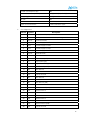
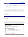
RELEASE NOTES
Version
1.00
1.01
Date
Jun. 27 2008
Sep. 3 2008
NOTES
Initial release
Support SDHC for WinCE 5.0
2
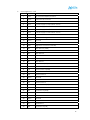
Table of Contents
1. Introduction ........................................................................................................................4
1.1 Package Contents ..............................................................................................................4
1.2 System Block Diagram.......................................................................................................5
2. Hardware............................................................................................................................6
2.1 CPU Module ..........................................................................................................................6
2.2 Base Board ..........................................................................................................................13
2.3 LCD Module ........................................................................................................................15
3 Development Environment Setup....................................................................................20
3.1 JDI Configuration...............................................................................................................20
4. Operation System ............................................................................................................24
4.1 WinCE 5.0.............................................................................................................................24
4.1.1 WinCE 5.0 Platform Builder Installation ...........................................................24
4.1.2 NXC2620 BSP Installation....................................................................................26
4.1.3 Make New WinCE 5.0 image with NXC2620 BSP .........................................27
4.1.4 Load New Platform Builder to NXC2620 DVK 3.2 .........................................31
4.1.5 Boot-up Options....................................................................................................35
4.1.6 ActiveSync and SD Card Driver Emulation....................................................35
4.1.7 Disk Drives on NXC2620......................................................................................36
4.1.8 WiFi Driver Installation .........................................................................................36
4.1.9 GPU SM502 Driver Installation ...........................................................................36
4.1.10 SDHC Driver Installation ....................................................................................37
4.2 Linux 2.6 ...............................................................................................................................38
4.2.1 Boot Loader Installation ......................................................................................39
4.2.2 Linux Kernel Installation ......................................................................................39
4.2.3 Root File System Installation ..............................................................................40
4.2.4 Linux Boot up options ..........................................................................................41
4.2.5 Tool Chain Installation.........................................................................................41
4.2.6 Create New Boot Loader....................................................................................42
4.2.7 Create New Linux Kernel....................................................................................42
5. BSP Download and Update.............................................................................................43
6. Electrical Characteristics ................................................................................................44
3
1. Introduction
By providing hardware and software solution, NCX2620 DVK 3.2 is designed to
comprise NXC2620 processor module, baseboard and LCD board as a developing
platform to accelerate time to market easily and immediately for targeting
application of HMI, Thin Client and SBC. DVK is inexpensive, feasible and high
performance development kit for evaluating the functionality and capability of
NXC2620 processor and system on module.
Thank you for choosing IC Nexus products!!
1.1 Package Contents
SODIMM200 CPU Card
NXC2620-PB260A or NXC2620-PB502A
Base Board
NXC2620-DVB32-BDA
LCD Board
NXC2620-DVB32-LB
LCD Module
5.7” or 7” LCD module
Power Adapter
AC 110/220 V (Input) to DC 5 V 3A (Output)
Battery Pack
Rechargeable Li-ion battery – 3.7 V, 1800 mAh
Ethernet Cable
RJ45 Ethernet cable
RS232 Cable
DB9-Female to DB9-Female null modem Cable
SD Card
1 GB or higher
Window CE 5.0 Serial Number
Microsoft Windows CE 5.0 License
4
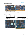
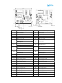
1.2 System Block Diagram
z
NXC2620-PB260A CPU Card (PCB08300)
3.3 V
1.8 V
Reset
NAND Flash
(8 bit)
3.3 V
Ethernet
PHY
256 Mb
256 Mb
256 Mb
256 Mb
256 Mb
Buffer
3.3 V
LCD I/F
CAM I/F
USB Host
USB Dev
SD / MMC
GPIO
PWM
I2S / AC97
UART
I2C
SPI
3.3 V memory
I/O Bus (16-bit)
10/100 Ethernet
256 Mb
256 Mb
NXC-2620
RTC
Vcc
256 Mb
SODIMM 200-pin edge finger
z
NXC2620-PB502A CPU Card (PCB08100)
3.3 V
1.8 V
Reset
NAND Flash
(8 bit)
3.3 V
Ethernet
PHY
NXC-2620
Buffer
RTC
256 Mb
SM502
GPU
Analog
VGA
LCD I/F
Video In/CIM
(8 bit)
3.3 V memory
I/O Bus (16-bit)
CAM I/F
USB Dev
USB Host
SD / MMC
GPIO
PWM
I2S / AC97
SPI
UART
I2C
10/100 Ethernet
Vcc
3.3 V
SODIMM 200-pin edge finger
z
NXC2620-DVB32-BDA Base Board (PCB08700)
USB Host
USB Dev
USB HUB
4 port
USB 1.1
Host
USB 1.1
Device
USB 2.0
Host OTG
USB 2.0
Device
USB 2.0
Device
Coin Cell
Battery
Ethernet
RJ45
AC97
SD MMC I/F
LCD I/F
header
LCD I/F
header
Audio
Codec
Speaker
Line In
Phone In
5.7 inch
16 bit I/O bus
Power
10 /100
Ethernet
Line out
SD Card
Holder
7 inch
Peripherals
Header
JTAG
COM 3
DB9
Vbat
NXC-2620-PB502 CPU Card
(SODIMM 200-pin)
COM 2
DB9
Analog RGB
VGA
(DB15)
COM 0
DB9
5
2. Hardware
Flexible and cost-effective solution, 32bit RISC core NXC2620 processor module is a
system on module designed to perform low power consumption embedded devices.
The OS support includes WinCE 5.0 and Linux 2.6. The on board PHY simplifies hardware
Ethernet connection.
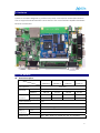
2.1 CPU Module
z Board Description
CPU Module
PB260A
PB260B
PB502A
PB502B
(PB08300)
(PB08310)
(PB8100)
(PB8110)
CPU Speed
Memory
336 MHz
NAND
128 MB
SDRAM
128 MB
64 MB
128 MB
64 MB
Display
LCD
YES
YES
YES
YES
Control
GPU(502)
NO
NO
YES
YES
JTAG Interface
YES
10/100 Ethernet PHY
YES
UART Interface
4, UART 0/debug port, UART 1/IrDA
USB 1.1
Host
1
Interface
Device
1
Peripherals
RTC, WDT, Timer, I2C, PWM, SPI, SSP, I2S, SD/MMC
6
z
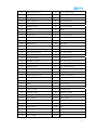
SODIMM200 Pin Assignment
¾
NXC2620-PB260A/B
3V
GND
GND
¾
NXC260-PB502A/ B
3V
GND
GND
7
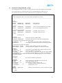
Pin NO
Pin Description
Pin NO
Pin Description
1
ENET_PWRFB
*1
2
Reserved3
3
ENET_TXD_N
*1
4
ENET_RXD_N
*1
5
ENET_TXD_P
*1
6
ENET_RXD_P
*1
7
ENET_100_LED
*1
8
ENET_10_LED
*1
10
EOP/GP27
12
DACK0/GP13
9
11
13
15
NC
RED Signal
*2
NC
RED Signal
*2
NC
Blue Signal
*2
NC
Blue Signal
*2
14
16
NC
GREEN Signal
*2
NC
GREEN Signal
*2
17
LCD_PCLK/GP58
*
18
LCD_DE/GP59
*
19
LCD_VSYNC/GP56
*
20
LCD_HSYNC/GP57
*
21
LCD_D[14]/GP54
*
22
LCD_D[15]/GP55
*
23
LCD_D[12]/GP51
*
24
LCD_D[13]/GP53
*
25
LCD_D[10]/GP50
*
26
LCD_D[11]/GP51
*
27
LCD_D[8]/GP48
*
28
LCD_D[9]/GP49
*
29
LCD_D[6]/GP46
*
30
LCD_D[7]/GP47
*
31
LCD_D[4]/GP44
*
32
LCD_D[5]/GP45
*
33
LCD_D[2]/GP42
*
34
LCD_D[3]/GP43
*
35
LCD_D[0]/GP40
*
36
LCD_D[1]/GP41
*
37
CIM_PCLK/GP10
*
38
CIM_MCLK/GP11
*
39
GND
40
Vbat(+3V3)
8
41
CIM_HSYNC/GP9
*
42
CIM_VSYNC/GP8
*
43
CIM_D[6]/GP6
*
44
CIM_D[7]/GP7
*
45
CIM_D[4]/GP4
*
46
CIM_D[5]/GP5
*
47
CIM_D[2]/GP2
*
48
CIM_D[3]/GP3
*
49
CIM_D[0]/GP0
*
50
CIM_D[1]/GP1
*
51
PPWR0/GP29
52
USB_CLK/GP28
53
DPLS0
54
DPLS1
55
DMNS0
56
DMNS1
57
Reserved1
58
OVC0/TEST_SEN
59
GND
60
VCC(+3V3)
61
XTAL
62
RESETOUT_
63
Reserved2
64
I2C_SDA
65
BITCLK/GP77
66
I2C_SCK
67
SDATA_IN/GP71
68
SSI_CLK/GP72
69
SDATA_OUT/GP70
70
SSI_CE1_/GP73
71
SYNC/GP78
72
SSI_DT/GP74
73
SYSCLK/GP68
74
SSI_DR/GP75
75
ACRESET_/GP69
76
SSI_CE2_/SPI_GPC/GP76
77
PWM1/GP95
78
PS2_KCLK/GP32
79
PWM0/GP94
80
PS2_KDATA/GP33
81
UART3_RTS/GP23
82
UART3_CTS/GP17
83
UART3_RxD_/GP16
84
UART3_TxD/GP21
85
UART2_RxD_/GP111
86
UART2_TxD/GP125
87
UART1_RxD_/GP24
88
UART1_TxD/GP25
89
UART0_RxD_/GP126
90
UART0_TxD/GP127
91
GND
92
VCC(+3V3)
93
PCE2_/GP93
94
Reserved4
95
PCE1_/GP90
96
PBVD2/GP89
97
PSKTSEL/GP91
98
INPACK_/GP88
99
WE3_
100
IOIS16_/GP92
101
WE1_/PIOR
102
WE2_/PREG_
103
WE_/PWE_
104
WE0_/PIOW_
105
FWE_/GP80
106
NC
107
FRE_/GP79
108
NC
109
RD_/POE_
110
NC
111
CS0_
112
NC
113
CS1_/GP83
114
NC
9
115
CS2_/GP84
116
NC
117
CS3_/GP85
118
NC
119
CS4_/GP86
120
NC
121
CS5_/GP87
122
NC
123
GND
124
VCC(+3V3)
125
A12
*3
126
A25
*4
127
A11
*3
128
A24
*4
129
A10
*3
130
A23
*4
131
A9
*3
132
A22
*4
133
A8
*3
134
A21
*4
135
A7
*3
136
A20
*4
137
A6
*3
138
A19
*4
139
A5
*3
140
A18
*4
141
A4
*3
142
A17
*4
143
A3
*3
144
A16
*4
145
A2
*3
146
A15
*4
147
A1
*3
148
A14
*4
149
A0
*3
150
A13
*4
151
GND
152
VCC(+3V3)
153
D15
*3
154
D31
155
D14
*3
156
D30
157
D13
*3
158
D29
159
D12
*3
160
D28
161
D11
*3
162
D27
163
D10
*3
164
D26
165
D9
*3
166
D25
167
D8
*3
168
D24
169
D7
*3
170
D23
171
D6
*3
172
D22
173
D5
*3
174
D21
175
D4
*3
176
D20
177
D3
*3
178
D19
179
D2
*3
180
D18
181
D1
*3
182
D17
183
D0
*3
184
D16
185
MSC_DAT[2]/GP36
186
MSC_DAT[3]/GP37
187
MSC_DAT[0]/GP34
188
MSC_DAT[1]/GP35
10
189
MSC_CLK/GP39
190
MSC_CMD/GP38
191
GND
192
VCC(+3V3)
193
Reserved5
194
Reserved6
195
RFIO
196
BT_FREQ
197
BT_ACTIVE
198
RX_CLEAR
199
GND
200
VCC(+3V3)
* NXC2620 & GPU SM502
*3 Bus Buffer – 74LVC16244
*1 Ethernet PHY
*4 Bus Switch – P13B16245A
*2 GPU SM502
z
Ethernet PHY –Single-Port 10/100M Fast Ethernet PHYceiver
The RTL8201CP is a single-port PHYceiver with an MII (Media Independent
Interface)/SNI (Serial Network Interface). It implements all 10/100M Ethernet
Physical-layer functions including the Physical Coding Sublayer (PCS), Physical
Medium Attachment (PMA), Twisted Pair Physical Medium Dependent sublayer
(TP-PMD),
with
an
auto
crossover
detection
function,
10Base-Tx
Encoder/Decoder, and Twisted Pair Media Access Unit (TPMAU).
A PECL (Pseudo Emitter Coupled Logic) interface is supported to connect with an
external 100Base-FX fiber optical transceiver. The chip utilizes an advanced
CMOS process to meet low voltage and low power requirements. With on-chip
DSP (Digital Signal Processing) technology, the chip provides excellent
performance under all operating conditions.
The RTL8201CP can be used for applications such as those for a Network
Interface Adapter, MAU (Media Access Unit), CNR (Communication and
Network Riser), ACR (Advanced Communications Riser), an Ethernet hub, and an
Ethernet switch. In addition, it can be used in any embedded system with an
Ethernet MAC that needs a UTP physical connection or Fiber PECL interface to an
external 100Base-FX optical transceiver module
z
Mobile Multimedia Companion Chip (SM502)
The SM502 is a Mobile Multimedia Companion Chip (MMCC™) device,
packaged in a 297-pin BGA and backward-compatible with the SM501.
Designed to complement needs for the embedded industry, it provides video
and 2D capability. To help reduce system costs, it supports a wide variety of I/O,
including analog RGB and digital LCD Panel interfaces, 8-bit parallel interface,
USB, UART, IrDA, two Zoom Video interfaces, AC97 or I2S, SSP, PWM, and I2C.
There are additional GPIO bits that can be used to interface to external devices
as well.
11
The 2D engine includes a front-end color space conversion with 4:1 and 1:8
scaling support. The video engine supports two different video outputs (Dual
Monitor), at 8-bit, 16-bit, or 32-bit per pixel and a 3-color hardware cursor per
video output. The LCD panel video pipe supports a back-end YUV color space
conversion with 4:1 and 1:212 scaling. A Zoom Video (ZV) port is also included to
interface to external circuitry for MPEG decode or TV input.
12
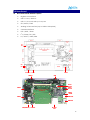
2.2 Base Board
z NXC2620-DVB32-DBA Description
¾
Digital LCD interface
¾
USB 1.1 Host / Device
¾
USB 1.1 / 2.0 Host Hub up to 4 ports
¾
SD / MMC / SDIO
¾
Analog VGA Interface (up to 1280 x 1024 pixels)
¾
Camera Interface
¾
RTC / WDT / Timer
¾
I2C / PWM / SPI / SSP
¾
I2S / AC97 / UART /IrDA
UART 0
VGA
Ethernet
RJ45
UART 2
Reset
Switch
CPU and LCD module Slot
SODIMM 200
UART 3
Power
DC Jack)
USB
Device
USB
Host
SPK 1
SD Card
Slot
SPK 2
IrDA (UART 1)
Line Out
USB HUB
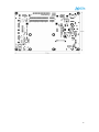
UART 0
VGA
Power
Socket
Power
DC Jack
UART 2
CPU and LCD module Slot
SODIMM 200
Battery
Socket
UART 3
USB Client
USB Host
IrDA (UART 1)
Line Out
SD Card
Slot
13
14
2.3 LCD Module
z NXC2620-DVB32-LB Description (PCB08900)
The LCD board supports 5.7 inch and 7 inch TFT LCD. Both TFT LCD panel are
support LED backlight and 4-wire resistance type touch signal input. It is designed
to support NXC2620 DVK 16-bit color LCD control with display pixel of 640(H) x
3(RGB) x 480(V) and 800(H) x 3(RGB) x 600(V).
199
z
1
5.7” LCD Panel – TFP507MWVGAHBE-03
¾
General specifications
ITEM
SPECIFICATION
Panel Size
5.7 inch (panel diagonal)
Display Area (mm)
116.16(W) x 87.12(H)
Number of Pixels
640 x 3(H) x 480 (V)
Pixel Pitch (mm)
0.1815(H) x 0.1815(V)
Color Pixel Arrangement
RGB vertical strip
Display Mode
Normally white
Number of colors
262,144
Viewing Direction
6 o’clock
Response Time (Tr + Tf)
30 ms
Brightness (cd/ m2)
180 nit(Typ)
NTSC ratio
50%
Viewing Angle (BL on, CR>=10)
140 degree(H), 100 degree(V)
Electrical Interface (data)
TTL
15
¾
Power consumption (W)
TBD
Outline Dimension (in mm)
127(W) x 100(H) x 7.65(D)
Weight (g)
~132g
BL unit
LED
Surface Treatment
Anti-Glare, Hardness:3H
Type of touch screen
4 Wire resistance type
Pin assignment
Pin NO
Symbol
Description
1
U/D
Up or Down Display Control
2
NC
Customer non-connect; initial pull high = DE mode
3
Hsync
Horizontal SYNC
4
VLED
Power Supply for LED
5
VLED
Power Supply for LED
6
VLED
Power Supply for LED
7
Vcc
Power Supply for LED
8
Vsync
Vertical SYNC
9
DE
Data Enable
10
X2
TSP control (Left)
11
Y1
TSP control (Up)
12
ADJ
Adjust for LED brightness
13
B5
Blue Data 5 (MSB)
14
B4
Blue Data 4
15
B3
Blue Data 3
16
Vss
Power Ground
17
B2
Blue Data 2
18
B1
Blue Data 1
19
B0
Blue Data 0 (LSB)
20
Vss
Power Ground
21
G5
Green Data 5 (MSB)
22
G4
Green Data 4
23
G3
Green Data 3
24
Vss
Power Ground
25
G2
Green Data 2
26
G1
Green Data 2
27
G0
Green Data 0 (LSB)
28
Vss
Power Ground
16
z
29
R5
Red Data 5 (MSB)
30
R4
Red Data 4
31
R3
Red Data 3
32
Vss
Power Ground
33
R2
Red Data 2
34
R1
Red Data 1
35
R0
Red Data 0 (LSB)
36
X1
TSP control (Right)
37
Y2
TSP control (Down)
38
DCLK
Clock signals
39
Vss
Power Ground
40
L/R
Left / Right Display control
7” LCD Panel – NFD70A-CIW-H
¾
General specifications
ITEM
SPECIFICATION
Display Area (mm)
152.4(W) x 91.44(H)
Number of Pixels
800(H) x 3(RGB) x 480 (V)
Pixel Pitch (mm)
0.1905(H) x 0.1905(V)
Color Pixel Arrangement
RGB vertical strip
Display Mode
Normally white
Number of colors
262,144
Viewing Direction
6 o’clock
Response Time (Tr + Tf)
20 ms
Brightness (cd/ m2)
250 nit(typ)
Viewing Angle (BL on, CR>=10)
140 degree(H), 110 degree(V)
Electrical Interface (data)
TTL
Power consumption (W)
2.5 W (Typ)
Outline Dimension (in mm)
165(W) x 104(H) x 6(D)
Weight (g)
~132g
BL unit
LED
Surface Treatment
Anti-Glare, Hardness:3H
Type of touch screen
4 Wire resistance type
17
¾
Pin Assignment – CN1
Pin NO
Symbol
Description
1
U/D
Up or Down Display Control
2
DMS
Selection DE or SYNC
3
Hsync
Horizontal SYNC
4
VLED
Power Supply for LED Driver circuit
5
VLED
Power Supply for LED Driver circuit
6
VLED
Power Supply for LED Driver circuit
7
Vcc
Power Supply for LED Driver circuit
8
Vsync
Vertical SYNC
9
DE
Data Enable Signal
10
AVss
Ground
11
AVss
Ground
12
ADJ
Brightness control for LED B/L
13
B5
Blue Data 5 (MSB)
14
B4
Blue Data 4
15
B3
Blue Data 3
16
Vss
Ground
17
B2
Blue Data 2
18
B1
Blue Data 1
19
B0
Blue Data 0 (LSB)
20
AVss
Ground
21
G5
Green Data 5 (MSB)
22
G4
Green Data 4
23
G3
Green Data 3
24
AVss
Ground
25
G2
Green Data 2
26
G1
Green Data 2
27
G0
Green Data 0 (LSB)
28
AVss
Ground
29
R5
Red Data 5 (MSB)
30
R4
Red Data 4
31
R3
Red Data 3
32
AVss
Ground
33
R2
Red Data 2
34
R1
Red Data 1
35
R0
Red Data 0 (LSB)
18
¾
36
AVss
Ground
37
AVss
Ground
38
DCLK
Clock signal
39
AVss
Ground
40
L/R
Left / Right Display control
Pin Assignment – CN2
Pin NO
Symbol
Description
1
XL
X axis resistance
2
YD
Y axis resistance
3
XR
X axis resistance
4
YU
Y axis resistance
19
3 Development Environment Setup
z
Development Environment Diagram
Development PC runs
Windows – HyperTerminal
Linux - minicom
USB Power Cable
RS232
NXC2620-DVB32-DBA
Base Board
JTAG
CPU Card
Target Board
Ethernet
¾
Connect development PC, JDI and Target Board to network
¾
Connect USB power cable between development PC and JDI
¾
Connect RS232 cable between development PC and Target Board
¾
Plug JDI JTAG cable to Target Board JTAG header
3.1 JDI Configuration
JDI
JTAG debugger
RS232 cable
PS2 to DB9-Female null modem Cable
Flat cable
2 x 7 flat cable
USB cable
JDI gets power supply via USB cable
Ethernet cable
Provides high data throughput for download OS image
* The JTAG debugger is not including in DVK 3.2 package.
JDI is a powerful and flexible JTAG debug tool for product development and
debugging. JDI can be used for Flash/EEPROM programming on the target board,
and device driver and OS low level debugging.
This section provides brief procedures of JDI setup. For detailed information on JDI
setup and command, please refer to the “JDI - JTAG Debug Interface User manual”.
To perform JDI configuration, only a USB power cable and an RS232 cable are
required to connect a JDI device.
20
Development PC runs
Windows – HyperTerminal
Linux - minicom
RS232 Cable
Only required at
when setting up
JDI parameters
for the first time.
USB Power Cable
z
Connect JDI to a development PC
¾
Connect USB power cable between development PC and JDI
¾
Connect RS232 cable between development PC and JDI
21
z
Prepare JDI configuration file – jdi.cfg
This configuration file is for JDI to communication with the target board. Please
use a text editor to create the file or use a sample file from DVK CD. It is
recommended that you create this file in TFTP root directory. A sample
configuration
file is provided as below:
;------------------------------------------------------------------------------------------------------------------------; JDI configuration file for the NXC-2600 development board
;-------------------------------------------------------------------------------------------------------------------------;
[INIT]
; Init INTC
WM32
0xB0001010
0xFFFFFFFF
; clear all intrs
WM32
0xB0001008
0xFFFFFFFF
; mask all intrs
; Init PLL
WM32
WM32
0xB0000000
0xB0000010
; Init memory controller
WM32
0xB0010070
WM32
0xB0010074
;
[HOST]
IP
192.168.1.20
;
[FLASH]
CHIPTYPE AM29
CHIPSIZE 0x00800000
0x10422220
0x50800120
; Clock Control Register0 (CPCCR0)
; PLL Control Register (CPPCR)
0x40000000
0x00005555
; GPALR2, GPIO as emc
; GPAUR2, GPIO as emc
; Flash type (AUTO|AM29|I28F)
; The size of the flash in bytes (for SST 8MB NOR)
; Parameters for chip type I28F and AM29
CHIPWIDTH
16
; The width of the flash chip in bits (8|16|32)
BUSWIDTH 16
; The width of the flash memory bus in bits (8|16|32)
; Parameters for chip type AM29
SETUPADDR1 0x555
; The first setup address of chip type AM29
SETUPADDR2 0x2AA
; The second setup address of chip type AM29
;
[NAND]
BUSWIDTH
8
; The width of the NAND flash chip in bits (8|16|32)
ROWCYCLES 2
; The row address cycles (2|3)
PAGESIZE
2048
; The page size of the NAND chip in bytes (512|2048)
FORCEERASE 0
; The force to erase flag (0|1). When set, all blocks
including that were marked as bad blocks will be erased. Don't set it during
normal operation.
;
[EEPROM]
ADDRESS
7
;The device address of EEPROM
;
[SDRAM]
BUSWIDTH
32
; The bus width of the SDRAM in bits (16|32)
BANKS
4
; The bank number (2|4)
ROWADDR
13
; Row address width in bits (11-13)
COLADDR
9
; Column address width in bits (8-12)
CASLATENCY
2
; CAS latency (2|3)
;
[GDB]
INITFILE gdbinit.bin
; Platform-dependent init code, required for gdb
debug
;
;; -- END --
22
z
Start TFTP service
TFTP service needs to be configured and started on host PC.
¾
For Windows
-
Install “SolarWinds-TFTP-Server.exe” from DVK CD
-
Enable TFTP server and configure IP address range to fall well within source &
destination IP. (File Æ Configure)
¾
For Linux
-
Use /tftpboot as the directory to provide TFTP service
-
Edit /etc/xinetd.d/tftp as following
service tftp
{
disable
= no
socket_type
= dgram
protocol
= udp
wait
= yes
user
= root
server
= /usr/sbin/in.tftp.d
……
}
-
Execute the following command to restart TFTP service
-
Copy file to “/tftpboot” directory as below
* Please disable firewall
23
4. Operation System
NXC2620 DVK 3.2 supports WinCE 5.0 and Linux 2.6 operation system. IC Nexus provide
Board Service Package (BSP) and source code for both operation systems on
NXC2620 DVK 3.2.
4.1 WinCE 5.0
z
z
System Requirement
¾
IBM compatible PC
¾
CPU 1.6 GHz or higher
¾
At least 30 GB free hard disk space or higher
¾
512 MB RAM higher
¾
OS: Microsoft Windows 2000 or newer
Software Requirements
¾
Microsoft Windows CE 5.0 IDE (Genuine licensed by Microsoft)
¾
UART communication tool – Microsoft HyperTerminal
¾
TFTP server (A free copy of Windows XP TFTP server software can be
download at http://www.solawinds.com/downloads)
4.1.1 WinCE 5.0 Platform Builder Installation
z
WinCE 5.0 Platform Builder
Obtain WinCE 5.0 Platform Builder from Microsoft. Then you can install the WinCE
5.0 with Platform Builder by using the genuine product key.
Then, follow installation instructions displayed on the host PC screen. There may
be pre-requisites such as .NET framework 1.1 which needs to be installed. Follow
the setup instructions carefully to ensure a CLEAN setup.
z
CPU support
Select the [Custom (Tools and OS)] choice to Install IDE and debugger support,
as well as CPU support for building images. Select “MIPS-II” CPU.
Click [Next>] button to continue installation. Once installation is complete, try to
“Open WinCE PB50 to check if the installation is OK. Close PB50 if it is OK”.
Ensure you do not encounter any problems with WinCE 5.0 Platform Builder.
24
z
Installing QFE (download from Microsoft website)
Microsoft frequently releases QFE(s) which contain very important updates for
WinCE Platform Builder. Please install the following QFE(s). It is strongly suggested
and is not “optional”.
¾
WinCEPB50-051231-Product-Update-Rollup-MIPSII.msi
¾
WinCEPB50-061231-2006M12-MIPSII.msi
¾
WinCEPB50-061231-Product-Update-Rollup-MIPSII.msi
¾
WinCEPB50-070131-2007M01-MIPSII.msi
¾
WinCEPB50-070208-KB931924-MIPSII.msi
¾
WinCEPB50-070228-2007M02-MIPSII.msi
¾
WinCEPB50-070331-2007M03-MIPSII.msi
¾
WinCEPB50-070430-2007M04-MIPSII.msi
¾
WinCEPB50-070531-2007M05-MIPSII.msi
¾
WinCEPB50-070630-2007M06-MIPSII.msi
¾
WinCEPB50-070731-2007M07-MIPSII.msi
¾
WinCEPB50-070831-2007M08-MIPSII.msi
¾
WinCEPB50-070930-2007M09-MIPSII.msi
¾
WinCEPB50-071031-2007M10-MIPSII.msi
¾
WinCEPB50-071231-Product-Update-Rollup-MIPSII.msi
¾
WinCEPB50-080131-2008M01-MIPSII.msi
¾
WinCEPB50-080229-2008M02-MIPSII.msi
¾
WinCEPB50-080331-2008M03-MIPSII.msi
¾
WinCEPB50-080531-2008M05-MIPSII.msi
25
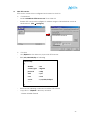
4.1.2 NXC2620 BSP Installation
Locate BSP archive on CDROM and install BSP as below …
¾
Copy BSP – “NXC2600DVK_Vx.x.x BSP” from CDROM to
“C:\WINCE500\PLATFORM\NXC2600DVB2” folder.
(Do this; if you install PB 5.0 in C drive else choose the disk drive where you
installed PB 5.0)
¾
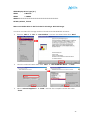
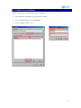
Execute “PB 5.0” Æ “File” Æ “Manage Catalog Items….” Æ “Import…”
¾
Identify the folder “NXC2600DVB2” in the –
“C:\WINCE\PLATFORM\NXC2600DVB2” and select “nxc2600dvb2.cec” file then
click “Open”. Catalog files will be imported and the new BSP will be show on the
list. Installing new BSP is complete. Verify that as shown in the screenshot below
then click “OK”.
26
4.1.3 Make New WinCE 5.0 image with NXC2620 BSP
IMPORTANT:Before cooking OS design, you have to set the choice for display type, script file
should be modified based on what features you need.
Check the file mentioned below for more details.
C:\WINCE500\PLATFORM\Nxc2600dvb2\Files\Script\ICNEXUS_DVB2.bat
NATIVE - display from CPU
SM502 - display from SM502 chip
Set the parameters correctly.
======================================
For 8100:
STEP 1:
Copy "SM502_sources" file from DVK 3.2 CD
\WinCE 5.0\NXC2600DVB2 BSP Beta 2
paste to
C:\WINCE500\PLATFORM\Nxc2600dvb2\Src\Bootloader
STEP 2:
Rename "SM502_sources" file to "sources" (no file name extension).
Overwrite any existing "sources" file.
STEP 3:
@REM*************************************************************
@REM Display Driver Type (0, 1)
@REM
0: NATIVE
@REM
1: SM502
@REM*************************************************************
SET BSP_DISPLAY_TYPE=1
Add SM502 driver as a catalog component into PB and add it to OS design, build OS
image
======================================
For 8300
STEP 1: Copy "NATIVE_sources" file from DVK 3.2 CD
\WinCE 5.0\NXC2600DVB2 BSP Beta 2
paste to
C:\WINCE500\PLATFORM\Nxc2600dvb2\Src\Bootloader
STEP 2: Rename "NATIVE_sources" file to "sources" (no file name extension).
Overwrite any existing "sources" file.
STEP 3:
@REM*************************************************************
27
@REM Display Driver Type (0, 1)
@REM
0: NATIVE
@REM
1: SM502
@REM*************************************************************
SET BSP_DISPLAY_TYPE=0
Make sure SM502 driver is NOT included in OS design. Build OS image
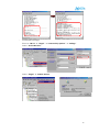
Create a new WinCE 5.0 image and bootloader with NXC2620 BSP as below…
¾
Execute “PB 5.0” Æ “File” Æ “New Platform” and see the wizard then click “Next”
¾
Choose a relevant name then click “Next” Æ “NXC2600DVB2: MIPSII” Æ “Next”
¾
Select “Internet Appliance” Æ “Finish” and see the complete wizard then click
“Finish”
28
* You can optionally choose “Mobile Handheld” but it is worth nothing that, some
device specific OS configuration might need some extra efforts in terms of shaping the
OS components including some device drivers which might need to be added /
removed as appropriate.
* We are trying to get a platform built quickly so no need at this stage to choose many
other features initially.
* Notice that the catalog contains the device drivers as well as the platform folders
contains similar items. If some item is missing in your platform it can be added from
catalog “drag and drop” or “right click options”.
¾
Form the menu, “Platform” Æ “Settings”
29
* Make sure the “Build Options” are select exactly as show in screenshot above. Avoid
choosing debug support options initially to speed up the PB 5.0 process.
* Configuration settings shall remain in RELEASE mode then click “OK”
¾
Select “Build OS” Æ “Sysgen”
* It may take 20 minutes for build procedure to complete. Be patient. Do not edit or do
random clicks on files in the “PB 5.0” during build process.
* There may be warning messages. Ignore them. There should be NO Errors in the build.
* Errors may arise due to several factors which include incorrect QFE updates or
incorrect BSP installation or corrupted “\\WINCE500\PUBLIC” folder files.
¾
Select “Build OS” Æ “Open Release Directory” and follow the path in Windows
Explorer and identify the following files.
Boot Loader:
-
Boot.map
-
Boot.nb0
OS Image:
-
NK.bin
* If you see these files on the “xxx Release” directory, you have successfully built a
30
platform out of the new BSP. Now you are ready to try load WinCE 5.0 OS on the
NXC2620 DVK 3.2 board.
4.1.4 Load New Platform Builder to NXC2620 DVK 3.2
¾
Adjust “boot.nb0” for writing to NAND Flash on DVK 3.2
Copy “boot.nb0” and “boot.map” files to TFTP root directory. Make sure
“MKBin.exe” is located in the exactly the same TFTP directory. Just as show below.
Notice the files.
Change directory to TFTP root and type “mkbin boot 0x83610000 K9F1G08U0A”.
“MKBin.exe” is used to adjust “boot.nb0” address so that “boot.nb0” so that
“boot.nb0” can be written to NAND Flash or NOR Flash.
¾
Prepare logo for writing to NAND Flash on DVK 3.2
Currently, only up to “640 x 480” resolution logo file can be used. Only bitmap
(*.bmp) file is supported right now. Sample logo file can be found in CDROM.
* Logo file size is restriction – 320 KB.
* Logo file is stored at 0x80 on NAND Flash.
¾
Download boot loader & logo to DVK 3.2
-
Please refer to chapter 3 to set-up development environment and start TFTP
Service first.
-
Telnet to JDI – “telnet xxx.xxx.xxx.xxx”
31
-
Download logo
JDI> nerase 0 500
JDI> nprog 0x80 logo-4.bmp
-
Download boot loader
JDI> nprog 0 boot.nb0
¾
Download WinCE 5.0 image
-
Connect RS232 cable between PC and NXC2620 DVK 3.2 console port.
-
Connect Ethernet cable to NXC2620 DVK 3.2
-
Execute “HyperTerminai”, 115200,n,8,1 then press “SPACE” key and hold.
-
Power on NXC2600 DVK 3.2 and see the boot loader menu as below. Now
you can release pressing “SPACE” key.
32
This is the starting point of boot loader and extensive configuration can be done
using menu option. Most of them are self explanatory.
-
Configure boot loader
ENABLE DHCP
Press [7] Network Settings Æ [2] Enable/Disable DHCP Æ [0] Exit and Continue
Select Download Device
Press [4] Select Download Device Æ [1] SDRAM
Select Boot Device
Press [5] Select Boot Device Æ [1] Ethernet
Select Save Settings
Press [8] Save and Restore Settings Æ [1] Save Current Settings Æ [0] Exit and
Continue
33
-
Download OS image
Execute “PB 5.0” Æ “Target” Æ “Connectivity Options” Æ “Settings”
Select “Active Devices”
Select “Target” Æ “Attach Device”
34
4.1.5 Boot-up Options
There are 2 ways to boot on NXC2620 DVB 3.2.
¾
SD card
-
In PB50, click "Build OS" --> "Open Release Directory" to open command line
window
-
Type “getnb0" to generate “nk.nb0” file.
-
Copy “ nk.nb0” into SD card. Then, insert SD card into the board’s SD slot.
-
Restart NXC2620 DVK 3.2.
* SD card has to be formatted in FAT32 format, “getnb0.bat” is a batch file, the WinCE
5.0 image size is specified in “-I 0x1E00000” (30 MB), if you build a WinCE size is more
than 30 MB, you should change the “-I” parameter. The next image size boundary falls
at 40 MB.
¾
NAND flash
Refer Chapter 4.1.4
4.1.6 ActiveSync and SD Card Driver Emulation
Active Sync USB device & SD card drive emulation functionality is inbuilt in
NXC2600DVB2 BSP and it is controlled by a flag. You can locate the file typically at the
following location
C:\WINCE500\PLATFORM\Nxc2600dvb2\Files\Script\ ICNEXUS_DVB2.bat
Open the file and edit the flags as shown below to allow Active Sync USB device
functionality or SD card drive emulation. Notice the ActiveSync flag is enabled now. It
can be changed to SD card by choosing the other flag. Only one can be enabled at
a time.
@REM*************************************************************
@REM USB Function Module
@REM
@REM If using the USB Function Module, such as ActiveSync, the
@REM environment variable BSP_NXC26_USBFN muse be set to 1.
@REM
@REM NOTES:
@REM
The two environment variable,
@REM
1. BSP_NXC26_USB_ACTIVESYNC
@REM
2. BSP_NXC26_MASS_STORAGE_SDMMC
@REM
@REM
CAN NOT set to 1 at the same time, as they use the same
@REM
USB port.
@REM
@REM*************************************************************
SET BSP_NXC26_USBFN=1
SET BSP_NXC26_USB_ACTIVESYNC=
SET BSP_NXC26_MASS_STORAGE_SDMMC=1
35
4.1.7 Disk Drives on NXC2620
Two disk drives one fixed and other removable can be found in the NXC2600DVB2
board.
¾
NAND flash (85 Mbytes)
¾
SD card (up to 2 GB)
SD card can be hot plugged. Storage Manager can access both the disks.
4.1.8 WiFi Driver Installation
Unzip the catalog components to a specific directory as below..
Qcom LR802UKG: C:\WINCE500\3rdparty\Qcom\LR802UKG
In the Platform Builder, import “QcomLR802UKG.cec” file.
EPSON WN6501CEP2: C:\WINCE500\3rdparty\EPSON\WN6501CEP2
In the Platform Builder, import “EPSON-WN6501CEP2.cec” file.
Ralink RT2501USB: C:\WINCE500\3rdparty\Ralink\RT2501USB
In the Platform Builder, import “RalinkRT2501USB.cec” file.
4.1.9 GPU SM502 Driver Installation
Unzip the catalog component to a specific directory as below..
SM502: C:\WINCE500\3rdparty\Silicon_motion\SMIVGX
In the Platform Builder, import “smivgx5.cec” file.
36
4.1.10 SDHC Driver Installation
Please follow steps to install SDHC driver as below…
¾
PB Æ Platform Æ Settings Æ Environment Æ New…
¾
Add “Variable name” Æ “IMGSDBUS2”
¾
Add “Variable Value ” Æ “1”
37
4.2 Linux 2.6
z
Files
Bootloader & Kernel Files
File Name
Describe
u-boot.bin
Boot loader for NOR Flash
u-boot-nand.bin
Boot loader for NABD Flash
uImage.kernel
Linux Kernel
Root File System
File Name
Describe
nxc2600-nfsroot-yyyymmdd.tar.bz2
NFS root file system
Nxc2600-sd-yyyymmdd.img
SD card image (Linux 2.6 root file system)
nxc2600-nand-yyyymmdd.tar.bz2
NAND root file system
Patch Files
File Name
Describe
Version
Linux-2.6.23-nxc2600-0.3.0-20080625-patch.bz2
Linux Kernel patch
0.3.0.
u-boot-1.2.0-nxc2600-0.3.0-20080625-patch.bz2
u-boot patch
0.3.0
Tool Chain
File Name
Describe
mipsel-linux-nxc2600-20071121.tar.bz2
Tool chain
Other Driver
File Name
rt73-cvs-2007111600.tar.bz2
Describe
Ralink rt2571wf driver
38
4.2.1 Boot Loader Installation
¾
Please refer to chapter 3 to set-up development environment and start TFTP
Service first.
¾
Connect JDI to Linux PC via USB cable. This provides JDI’s power supply.
¾
Connect JDI to network via Ethernet cable.
¾
Connect JDI to DVK 3.2 board JTAG port.
¾
Connect Linux PC to DVK3.2 board UART 0 via RS232 cable.(Default console
port is UART 0 on DVK 3.2 board)
Note: Alpha2 or later, default console port change to UART 0
¾
Execute “minicom” on Linux PC – 57600/8N1
¾
Power ON DVK 3.2 board
¾
Telnet to JDI – telnet 192.168.1.201
¾
Boot up from NAND Flash
JDI> nerase 0 2
JDI> nprog 0 u-boot-nand.bin
¾
Execute “minicom” on Linux PC – 57600/N81 then press “RESET” button on
DVK 3.2 board to restart boot loader. Then see the prompt as below…
NXC2600#
Note: User can update boot loader as below…
NXC2600#run update_b
4.2.2 Linux Kernel Installation
¾
Default network parameters of boot loader as below
Host IP: 192.168.1.3
Server IP: 192.168.1.60
¾
Change Host IP and Server IP as below
NXC2600# set ipaddr 192.168.xxx.xxx
NXC2600# set serverip 192.168.xxx.xxx
NXC2600# save
¾
Execute command to update Linux kernel as below…
NXC2600#run update_k
¾
Execute “minicom” on Linux PC – 57600/N81 then press “RESET” button on
DVB2 board to restart Linux kernel. Then see the message as below…
Waiting for root device /dev/mmc1k0p2…
39
4.2.3 Root File System Installation
¾
Root File System on SD card
-
Create 2 partitions in SD card, use “fdisk” to create partitions.
#fdisk /dev/mmcblk0
-
First partition: FAT format for demo files.
1. User can put any demo files (*.jpg, *.mp3 etc…) into this partition.
2. This partition mounts on /mnt/demo in NXC2600 platform system.
-
Secind partition: Root File System, 120 MB or higher and install as below…
#dd if=/path/to/rootfs.img of=/dev/mmcblk0p2
¾
Root File System on NAND Flash
-
untar the file “nxc2600-nand-20080625.tar.bz2” on Linux PC
#tar jxvf /path/to/nxc2600-nand-20080625.tar.bz2 –C /nfsroot/nxc2600
- copy all files into NAND Flash on nxc2600 DVK 3.2
#mount /dev/mtdblock3 /mnt –t yaffs2
#cp –dprR /nxc2600-nand/* /mnt
#umount /mnt
x
40
4.2.4 Linux Boot up options
There are 2 ways to boot up Linux on NXC2600 platform.
¾
Normal Boot Up (default bootup)
NXC2600# run defaultboot
¾
NFS Boot Up
NXC2600# run nfsboot
by default the nfsroot entry is "serverip:/nfsroot/nxc2600". change entry by:
NXC2600# set nfsargs set bootargs mem=\${memsize} console=\${console}
root=/dev/nfs rw ip=\${ipaddr} nfsroot=\${serverip}:/path/to/nfsroot
NXC2600# save
¾
NAND Flash Boot Up
NXC2600# run nandboot
NOTE: if u-boot is not bootup program, you must pass mtd
device partitions for system's offset by:
NXC2600# set nandargs set bootargs mem=\${memsize}
console=\${console} root=/dev/mtdblock3 rw ootfstype=yaffs2
mtdparts=nxc2600-nand:256k@${rootfs_addr}(uboot)ro,256k(p
arams),2048k(kernel),-(rootfs)
NXC2600# save
4.2.5 Tool Chain Installation
¾
Tool chain install as below…
#tar jxvf /path/to/mipsel-linux-nxc2600-20071121.tar.bz2 –C /
¾
Set Path
#set PATH=$PATH:/opt/toolchain/mipsel-linux/bin
or
#export PATH=/opt/toolchain/mipsel-linux/bin
41
4.2.6 Create New Boot Loader
¾
Download u-boot(ver 1.2.0) source file - u-boot-1.2.0.tar.bz2 from
http://www.denx.de/wiki/UBoot
¾
Install u-boot source file to /path/to/u-boot-1.2.0 as below…
#tar xjvf /path/to/u-boot-1.2.0.bz2 –C /path/to/u-boot-1.2.0
¾
Install u-boot patch file as below…
#cd /nxc2600/u_boot/u-boot-1.2.0
#bzcat /path/to/u-boot-1.2.0-NXC2600-0.3.0-20080625-patch.bz2
|patch –p1
¾
Create boot loader to boot up from NOR flash
#cd /path/to/u-boot-1.2.0
#make distclean
#make nxc2600_dvb2_config
#make
#cp u-boot.bin /tftpboot/
¾
Create boot loader to boot up from NAND flash
#cd /path/to/u-boot-1.2.0
#make distclean
#make nxc2600_dvb2_nand_config
#make
#cp u-boot-nand.bin /tftpboot/
4.2.7 Create New Linux Kernel
¾
Download Linux kernel(ver 2.6.23) source file – linux-2.6.23.tar.bz2 from
http://kernel.org
¾
Install Linux kernel source file to /path/to/linux-2.6.23 as below…
#tar xjvf /path/to/linux-2.6.23.tar.bz2 –C /path/to/linux-2.6.23
¾
Install Linux kernel patch file as below…
#cd /path/to/linux-2.6.23
#bzcat /path/to/linux-2.6.23-NXC2600-0.3.0-20080625-patch.bz2
|patch –p1
¾
Create Linux kernel
#cd /path/to/linux-2.6.23
#cp arch/mips/defconfig .config
#make uImage
42
5. BSP Download and Update
Please apply ID and password from our website first. Then download & update the
latest WinCE 5.0 / Linux 2.6 BSP from the website.
IC Nexus website: http://www.icnexus.com.tw/icnexus02/member.php
43
6. Electrical Characteristics
Standard Battery
Rechargeable Li-ion battery – 3.7 V, 1800 mAh
Backup Battery
3 V, 5 mAh, Coin Cell Battery
Power Adapter
AC 110/220 V (Input) to DC 5 V 3A (Output)
44