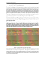
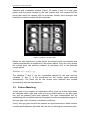
1
Automatic Detection and Localization of Logic Gates using Image Recognition TITLE: Automatic Detection and Localization of Logic Gates using Image Recognition MASTER DEGREE: Master in Science in Telecommunication Engineering & Management AUTHOR: Albert Martin Cirera DIRECTOR: Dr. Francesc Tarrés Ruiz DATE: November 25th 2013 2 Automatic Detection and Localization of Logic Gates using Image Recognition Overview The main objective of this Master Thesis is to design and develop a software application for logic gates detection and localization in the cell layer of a microchip. In order to extract the images of a microchip it is necessary to attack the microchip with mechanical polishing or chemical attack and take pictures from the inside. The result is the extraction of four layers with their respective images, including the cell layer where the logic gates are defined. This image of the cell layer is very large and could store tens of thousands of logic gates. This thesis proposes efficient image processing methods for finding and identifying the logic gates in the reconstructed image of the cell layer. To achieve these objectives, it takes a sample or pattern of each logic gate to define a logic gate database. Then the correlation between the pattern and the corresponding area of the cell layer is performed, covering the entire cell layer to find more match points. Resumen El objetivo principal de esta Master Tesis es diseñar y desarrollar una aplicación de software para la detección y localización de puertas lógicas en la capa de celdas de un microchip. Donde forma parte la ingeniería inversa de este. Para extraer las imágenes de la capa de celdas de un microchip es necesario atacar el microchip con un pulido mecánico o ataque químico, para así llegar a las capas más profundas de este y entonces tomar fotografías del interior. El resultado es la extracción de varias capas con sus respectivas imágenes, incluyendo la capa de celdas, que es donde se encuentran las puertas lógicas. Esta imagen de la capa de celdas es la unión de muchas fotografías unidas y el resultado es una imagen de gran tamaño que almacena decenas de miles de puertas lógicas. Esta tesis propone métodos de procesamiento de imágenes para la detección y la localización de las puertas lógicas, en la imagen reconstruida de la capa de celdas. Para lograr estos objetivos, se toma una muestra o patrón de cada puerta lógica, obteniendo así una base de datos con cada una de las puertas lógicas existentes, denominado patrón. A continuación, se realiza la búsqueda con el patrón por la capa de celdas, para detectar y localizarlas de forma automática. 4 Automatic Detection and Localization of Logic Gates using Image Recognition Index CHAPTER. 1 INTRODUCTION ....................................................................... 1 1.1. State of the Art ...................................................................................... 1 1.2. Reverse Engineering in an IC ............................................................... 1 1.2.1. The Internal Structure of a Microchip .............................................. 2 1.2.2. How to Access the Inside of the IC ................................................. 2 1.3. Image Processing Applied to Reverse Engineering .............................. 3 1.3.1. Image Mosaic ................................................................................. 3 1.3.2. Detecting and Locating the Logic Gates ......................................... 3 CHAPTER. 2 IMAGE PROCESSING IN IC REVERSE ENGINEERING ......... 6 2.1. Mechanical Polishing............................................................................. 6 2.2. Image Mosaic ........................................................................................ 7 2.3. Problem Statement.............................................................................. 11 2.4. Inputs for Logic Gate Detection and Localization ................................ 11 2.4.1. Logic Gate Cell Layer ................................................................... 11 2.4.2. Row of Logic Gates ...................................................................... 12 2.4.3. Logic Gate Pattern ........................................................................ 14 2.4.4. Logic Gate Contact Points ............................................................ 15 2.4.5. Pattern Mask................................................................................. 16 2.4.6. Pattern Template .......................................................................... 17 2.5. Outputs for Logic Gate Detection and Localization ............................. 17 CHAPTER. 3 DETECTING AND LOCATING LOGIC GATES ....................... 18 3.1. Row Splitting ....................................................................................... 18 3.1.1. Strategy for Finding Logic Gate Rows .......................................... 18 3.2. Finding Contact Points ........................................................................ 21 3.2.1. Pre-processing Logic Gate Rows ................................................. 21 3.2.2. The Algorithm for Finding Contact Points ..................................... 23 3.2.3. Algorithm for Finding Contact Points in a Pattern ......................... 24 3.3. Pattern Matching ................................................................................. 25 3.3.1. Pre-processing Logic Gate Row and Pattern Energy ................... 27 3.3.2. Energy derivative of the Image Rows and Patterns ...................... 27 3.3.3. XOR Filter ..................................................................................... 29 3.3.4. Energy derivative Filter Correlation............................................... 30 3.3.5. Correlation between the Pattern and Region to be evaluated ...... 32 CHAPTER. 4 EVALUATION AND RESULTS ................................................ 33 4.1. Contact Point Dithering ....................................................................... 33 4.2. Contact Point Results .......................................................................... 35 4.3. Results Match ..................................................................................... 36 4.4. Processing Time ................................................................................. 38 4.5. Outputs................................................................................................ 39 CHAPTER. 5 DATA STRUCTURE AND USER INTERACTION ................... 41 5.1. File Structure ....................................................................................... 41 5.2. User Interaction ................................................................................... 42 5.2.1. Graphic Interaction for the Threshold Specifications .................... 42 5.2.2. User Interaction for the Command Line ........................................ 43 5.3. User Interaction Load Evaluation ........................................................ 45 CHAPTER. 6 CONCLUSIONS & FUTURE WORKS ..................................... 47 CHAPTER. 7 REFERENCES ........................................................................ 48 ANNEXES 49 ANNEX 1. Structure folders........................................................................ 49 ANNEX 2. User Manual.............................................................................. 53 Index of figures Figure 1.1 The structure of a microchip. ............................................................. 2 Figure 1.2 The layers of a microchip. ................................................................. 4 Figure 2.1 An example captured image. ............................................................. 7 Figure 2.2 Example mosaic. ............................................................................... 8 Figure 2.3 Example of some problems appearing following capture errors. ....... 9 Figure 2.4 Example of some problems appearing following capture errors. ....... 9 Figure 2.5 Example of some problems appearing following capture errors. ..... 10 Figure 2.6 Example of a propagation problem.................................................. 10 Figure 2.7 Cell layer. ........................................................................................ 12 Figure 2.8 Zoomed image of a cell layer to show the rows. ............................. 13 Figure 2.9 Sample rows. .................................................................................. 13 Figure 2.10 Zoomed image of the cell layer to see the logic gate. ................... 14 Figure 2.11 Similarity between logic gates. ...................................................... 15 Figure 2.12 Contact points of an INV logic gate. .............................................. 15 Figure 2.13 Logic gate region more susceptible to being eliminated. ............... 16 Figure 2.14 Inv & DFFSR masks. ..................................................................... 16 6 Automatic Detection and Localization of Logic Gates using Image Recognition Figure 2.15 Inv & DFFSR templates. ................................................................ 17 Figure 3.1 Image of part of two rows of logic gates. ......................................... 19 Figure 3.2 Results of the energy derivative. ..................................................... 20 Figure 3.3 Cell layer energy derivative. ............................................................ 20 Figure 3.4 Difference in row brightness. ........................................................... 21 Figure 3.5 Result of row pre-processing. .......................................................... 23 Figure 3.6 Histogram of the row. ...................................................................... 23 Figure 3.7 Histogram of a processed row. ........................................................ 24 Figure 3.8 Pattern contact points...................................................................... 25 Figure 3.9 Filters for matching logic gates. ....................................................... 26 Figure 3.10 Filters for matching logic gates. ..................................................... 27 Figure 3.11 Part of one row and the result of the energy derivative. ................ 28 Figure 3.12 The energy derivative and binary pattern. ..................................... 29 Figure 3.13 The energy derivative and binary candidate. ................................. 30 Figure 3.14 The energy derivative of the pattern. ............................................ 31 Figure 3.15 The energy derivative of the candidate. ........................................ 31 Figure 3.16 Matrix correlation. .......................................................................... 32 Figure 4.1 Large logic gate. .............................................................................. 33 Figure 4.2 Medium logic gate. .......................................................................... 33 Figure 4.3 Small logic gate. .............................................................................. 34 Figure 4.4 Contact point dithering. ................................................................... 34 Figure 4.5 Contact points found. ...................................................................... 35 Figure 4.6 Results of the correlation without filters and contact points. ............ 36 Figure 4.7 Results of the correlation with contact points. ................................. 37 Figure 4.8 Results of the correlation with filters and contact points. ................. 37 Figure 4.9 File ‗out.txt‘. ..................................................................................... 39 Figure 4.10 File ‗LogicGatesLocation.xml‘. ....................................................... 40 Figure 4.11 Image of the row of logic gates...................................................... 40 Figure 5.1 Structure of folders and scripts. ....................................................... 41 Figure 5.2 Image of the row of logic gates........................................................ 42 Figure 5.3 Image of insert CP........................................................................... 43 Figure 5.4 Image of a pattern and candidate compared. .................................. 43 Figure 5.5 Image of the command line of the script ‗divideImgIntoRows‘. ........ 44 Figure 5.6 Image of the command line of the script ‗searchContactPoints‘. ..... 44 Figure 5.7 Image of the command line of the script ‗setPatternContactPoints‘. 44 Figure 5.8 Image of the command line of the script ‗logicGatesDetection‘. ...... 45 Figure 5.9 Image of the command line of the script ‗generateOuputFiles‘. ....... 45 Figure 5.10 Comparison between numbers of ‗Yes‘ and ‗No‘s‘. ....................... 45 Figure A.1 Structure INPUTS. .......................................................................... 49 Figure A.2 Structure INF. ................................................................................. 51 FigureA.3 Format TXT. ..................................................................................... 52 Figure A.4 Format XML. ................................................................................... 52 Figure A.5 Image result .................................................................................... 52 Figure A.6 Image result. ................................................................................... 53 Figure A.7 Scripts MATLAB.............................................................................. 53 Figure A.8 Energy of the derivate of the all rows in the cells layer ................... 54 Figure A.9 Contact Points of rows .................................................................... 54 Figure A.10. Contact Points of pattern ............................................................. 55 Figure A.11. Row mirror or not mirror. .............................................................. 55 Figure A.12 Check pattern ............................................................................... 56 Figure A.13 Insert pattern ................................................................................. 57 Index of tables Table 3.1 XOR.................................................................................................. 30 Table 4.1 Values of the correlation according to the displacements. ................ 34 Table 4.2. Contact points in the row. ................................................................ 35 Introduction 1 CHAPTER. 1 INTRODUCTION This master's thesis project arose out of the integrated circuit (IC) reverse engineering project [5,6] undertaken at the Spanish National Microelectronics Center (CNM, as it is known by its Spanish acronym). The aim is to reconstruct a wiring diagram of a microchip using the very same microchip. It must be noted that there is only one microchip available to do the reverse engineering so any error could be fatal to the fulfillment of the objective. In order to achieve this objective and simplify the entire internal visualization system of the microchip, image-processing tools are developed [1] to automate processes previously done manually with other microchips in other projects. These processes consist of capturing photographs of the internal structure of the microchip and combining the photographs comprising the structure in a single image using image processing. In order to facilitate the internal analysis of the microchip, the image previously obtained is then processed so as to detect and locate the elements with which it was formed. 1.1. State of the Art Some relevant examples from the bibliography available of the state of the art are examined in order to generally identify the investigative and analytical attention given to this area in scientific reports. Given that an exhaustive review of the bibliography available was not possible, the focus was on the following documents: Recognition of Integrated Circuit Images in Reverse Engineering [7]; this publication proposes an automatic recognition method for IC elements and for obtaining a description of the IC based on an image of one layer of the very same IC. The method offers noise stability and a low error rate. In order to speed up the processing, special algorithms are developed to detect contours, vectorize the image and reconstruct the vector representation. Reverse Engineering of CMOS Integrated Circuits [8]; this publication proposes reverse engineering methods for an IC using visual data of the IC connections layer. It also provides the results obtained from the experimental testing of the methods proposed and presents a brief overview of the reverse engineering methods currently known. 1.2. Reverse Engineering in an IC Reverse engineering in an integrated circuit means obtaining the design for the wiring diagram of a microchip for the purpose of determining how it works. The method is known by this name because it unfolds in the opposite direction of 2 Automatic Detection and Localization of Logic Gates using Image Recognition habitual engineering tasks, which consist of using technical data to create a certain product. Reverse engineering is a problem solving method and applying it to something involves an in-depth study of how the object works until said mode of operation can be understood, modified and improved. 1.2.1. The Internal Structure of a Microchip Integrated circuits are made of silicon as the base for the arrangement of different circuit elements such as transistors, diodes and resistors. They contain hundreds or thousands of these components distributed in an organized manner. During manufacturing, these regions are interconnected by means of tiny conductors in order to produce complex specialized circuits. Once built, a microchip is enclosed in a plastic or ceramic capsule containing the connector pins to the external circuitry. Figure 1.1 shows a diagram of the parts that comprise a simple microchip. More complex microchips can feature more cell and connection layers or even different memories or analog circuits. Figure 1.1 The structure of a microchip. Several layers can be found upon accessing the inside of a microchip. The first layer is the encapsulation that covers the microchip. One or several socket layers can be found deeper down as well as the cell layer and digital circuitry (where the logic gates are located). 1.2.2. How to Access the Inside of the IC There are different approaches to accessing the inside of a microchip to be able to capture the entire internal structure: Introduction 3 - The first consists of a chemical attack. Different acids are applied to the surface of the microchip to destroy the first layers and reach the silicon. The attack is done several more times until all of the layers have been captured. - The second type of approach, which is the one that was used with the microchip in this thesis, involves mechanical polishing. This approach wears down the surface to reach each one of the layers. As the attack progresses and the deeper inside the microchip, the layers may be observed and digital images of the layers captured to obtain the information on the internal structure. These include the socket and cell layers. 1.3. Image Processing Applied to Reverse Engineering Mechanical polishing, which gradually erodes the microchip, destroys the encapsulation to reach one of the layers and capture photographs of the entire layer. Image processing is used after this point to speed up the entire reverse engineering analysis. 1.3.1. Image Mosaic Once all of the photographs of a microchip layer have been captured, the first image-processing step is taken. It consists of reconstructing the image of the entire layer as if it were a puzzle. To do so, contiguous images must be overlapped to find the shared regions between the images in order to combine them. This image processing results in complete images of each and every one of the layers obtained in the reverse engineering of the IC. With this step, you obtain a large-size image for each layer, which contains all of the visual information on the connections, and another large-size image containing all of the visual information on the logic gates. 1.3.2. Detecting and Locating the Logic Gates This thesis focuses on the digital circuitry layer (where the logic gates are located), which is also known as the cell layer. This means the previously reconstructed image will be the baseline image used for the analysis package developed in this project. This layer contains all of the logic gates comprising the microchip where tens of thousands of logic gates may be found of all different sizes and varying degrees of complexity. The quantity of logic gates means it is necessary to seek alternatives for their automatic search. The image obtained from the cell layer is analyzed before doing any image processing. The integrated circuit design architecture concentrates most of the 4 Automatic Detection and Localization of Logic Gates using Image Recognition logic gates horizontally meaning the first step in the analysis system will be to detect this type of geometric logic gate arrangement. Figure 1.2 shows a diagram of the result of the cell layer image where the logic gate rows are arranged horizontally and the logic gates inside each one of the rows are marked in rectangles of different sizes and colors indicating the different logic gates. Figure 1.2 The layers of a microchip. The large size of the cell layer image makes it difficult to do any type of processing directly with the complete cell layer image. Taking advantage of the horizontal formation of the logic gates with respect to the cell layer image, the first step is to automatically identify the positioning of each one of the rows in order to later cut out the image. The result is an image for each one of the logic gate rows. This makes for smaller sized images for easier processing. A database needs to be obtained with a sample for each logic gate existing in the cell layer, known as a pattern, in order to detect and locate the logic gates. Each pattern is used to detect and locate the rest of the gates of the same type of logic within each one of the cell layer rows. To do so, each pattern is placed over the top of each one of the images of the logic gate rows to compare the pattern with the overlapped region of the logic gate row of the same size as the pattern. The time it takes to place each one of the patterns existing in the cell layer over all of the existing logic gate rows searching for similarity between the region and the pattern requires a large number of calculations. Pearson‘s correlation coefficient is calculated [3] between each region and pattern to assess the similarity. Given the average time it takes to move a pattern over the entire row, the estimated processing time for all of the patterns and all of the logic gate Introduction 5 rows exceeds one year. Considering that the work is done with a second generation Intel i5 processor, alternatives are sought to drastically reduce this time. Elemental components are sought with all shared logic ports in order to reduce the processing time. These parts are the contacts between the logic ports and the connections, which are known as contact points. By searching for the contact points in all of the logic gate rows and marking several contact points for each one of the patterns, only those areas of the logic gate row that coincide with the pattern contact points are evaluated. This strategy drastically reduces the overall processing time by over 100 times to obtain a total processing time of less than one week. Once an entire logic gate row has been completed, the result is verified and stored in different files. The purpose of each one of the files, as defined by the CNM, is to demonstrate the final results in a visual, written and comprehensible manner for any future software that requires these results. An overall perspective of the problem this thesis centers on will be presented in Chapter 2. All of the components used throughout the project and the outputs obtained will be discussed in detail. All of the algorithms and strategies used throughout the project will be presented in Chapter 3. Starting with the cell layer, a logic gate row is extracted and similarities are sought with the logic gate example. The difficulties encountered when developing the project and how each one of them was resolved will be presented in Chapter 4. The results obtained in the search for contact points will also be discussed. The general structure of all software organization and how the files containing the variables can be modified will be briefly presented in Chapter 5. Moreover, the interaction between users and the software will be explained. Finally, the overall conclusions drawn throughout the project and areas for future improvement will be presented in Chapter 6. 6 Automatic Detection and Localization of Logic Gates using Image Recognition CHAPTER. 2 IMAGE PROCESSING IN IC REVERSE ENGINEERING A global perspective of the entire reverse engineering process is presented throughout this chapter. Everything from how to access the inside of a microchip, how to capture photographs of the internal structure, reconstructing all of the photographs of a single layer in a single image to detecting logic gates to obtain the electronic diagram will be discussed. The attack used in this reverse engineering project consisted of mechanical polishing with which the internal structure of the microchip can be accessed. Once the mechanical polishing deepens to one of the microchip layers, photographs of that layer are captured in order to obtain a complete image for each one of the layers comprising the structure. Immediately thereafter, mechanical polishing is again used to access another layer and the same procedure is done with all of the layers constituting the microchip. All of the images processing procedures to be applied to resolve the problem are explained below. Firstly, the process of how to combine and situate all of the photographs of a single layer in order to form a single image of the entire layer automatically is explained. Although this process is not part of this thesis, it is summarized due to the fact that one of the resulting images, the cell layer image, is the information used as a starting point for the automatic analysis of the logic gates which is the focus of this work. On the one hand, the necessary inputs throughout the project are outlined as well as the image of the cell layer, the images of the logic gate rows, the patterns, the masks and the templates. On the other hand, the output files showing the results obtain when detecting and locating the logic gates are defined. 2.1. Mechanical Polishing Mechanical polishing consists of mechanically destroying the upper layers of the microchip in order to access the internal structure. To do so, all of the encapsulation and coating is destroyed first to reach the different layers comprising it. Figure 2.1 shows two contiguous photographs taken of the socket layer. Image processing in IC reverse engineering 7 Figure 2.1 An example captured image. Photographs are taken with a zoom not specified by the CNM and with a resolution of 3000x3800 pixels of the entire layer and the polishing process is repeated until the following layer is reached where photographs are once again taken of the entire layer. This process is repeated for all of the layers comprising the microchip. It is important to underline that when taking photographs; there must be a certain degree of overlapping between contiguous regions in order to be able to do the image processing to automatically detect the proper position of the combination of both photographs. 2.2. Image Mosaic The essential objective at this point is to automatically locate and join all of the photographs comprising a single layer of the microchip as if it were a puzzle. The same process is done for each one of the layers of the microchip structure. To do so, it is very important for the contiguous photographs taken of a single layer to share an overlapped region. Using Figure 2.2 as an example, the region marked in blue is the overlapped region between both images. In order to establish the positioning (connection) between the images in Figure 2.2, the region in yellow in the left image is placed over the region in red in the right image. Each time one is placed over another, Pearson‘s correlation coefficient is calculated between the region marked in yellow in the left image and the corresponding region in the right image. The result with the highest value between all of the correlations determines the overlapping position automatically. With the example in Figure 2.2, the highest correlation is obtained with the region marked in yellow on the left image and the region marked in yellow on the right one. 8 Automatic Detection and Localization of Logic Gates using Image Recognition Figure 2.2 Example mosaic. The entropy calculation is added in order to differentiate the correlations with a high value generated by regions with a high noise level. The entropy value for the region to be evaluated grows in noisy environments so the result of the division between the correlation and the entropy differentiates regions with high noise levels. The result of this image processing is the reconstruction of an entire layer of the microchip in image format. Even still, all of the problems encountered must be considered both for the reconstruction of the entire layer as well as the possible consequences for the resulting image since one of these images is the cell layer which is the entry point for detecting and locating the logic gates. The first cause found is excessive mechanical polishing or non-consistent polishing in a single region. Another cause is the view through the microscope not being even on the ends when capturing the photographs of a layer, which produces minor variations in scale between the contiguous photographs. Finally, one more cause is taking contiguous photographs without any overlapped region between them or even leaving blank areas between the photographs taken. All of these causes make it impossible to reconstruct this region of the layer and can even make it difficult to detect and locate the logic gates. After capturing the photographs, image deformations were observed on the ends of the image caused by the microscope lens. As can be seen in Figure 2.3, which shows two contiguous photographs of one of the microchip layers, the area marked in red on the left image should have been equal to the area marked in red on the right image. These deformations caused by the microscope lens make it difficult to combine both images automatically. Image processing in IC reverse engineering 9 Figure 2.3 Example of some problems appearing following capture errors. One mechanical polishing problem is that it is not consistent over an entire layer. As a result, there are regions that are more polished than others. Such is the case that some regions of a layer have been destroyed. Figure 2.4 shows two contiguous images of the same layer. The mechanical polishing in the right image is deeper than that of the left image. Moreover, the region where the two images overlap, which are marked in red show different levels of deepness in the polishing indicating that mechanical polishing was done between the two captures. Figure 2.4 Example of some problems appearing following capture errors. Another problem encountered throughout the image reconstruction of one of the layers is the similarity between some of the regions. For example, Figure 2.5 shows how the link between images is located between the region marked in white on the left image and the red region on the right image. But, it can be clearly observed that the white region on the right image will show a similar 10 Automatic Detection and Localization of Logic Gates using Image Recognition correlation result with the red region due to the similarity. This can lead to the left image being situated incorrectly. Figure 2.5 Example of some problems appearing following capture errors. Chain errors occur as a result of these problems. For example, the middle region marked in red in Figure 2.6 is situated in an incorrect position, which means the following photographs of the layer will also be situated incorrectly. Figure 2.6 Example of a propagation problem. All of the problems explained above make it difficult to automatically reconstruct the entire image of the layers comprising the microchip. This means user Image processing in IC reverse engineering 11 interaction is necessary in some sections of the reconstruction in order for it to be done properly. 2.3. Problem Statement The main objective, which is the subject of this thesis, is detecting and locating the logic gates in the cell layers of a microchip. Due to the large number of logic gates the microchip contains, software is developed to detect and locate them automatically. To do so, all of the inputs required as well as all of the components needed to detect them will first be outlined in detail. Finally, the ensemble of files providing the results obtained will be specified in order to interact with other reverse engineering sub-systems. 2.4. Inputs for Logic Gate Detection and Localization The complete cell image with all of the logic gate rows containing all of the logic gates is needed to detect and locate the logic gates. The patterns used for each one of the logic gates existing in the cell layer and the contact points contained in each one of the logic gates are also defined. On the other hand, the pattern masks are defined, which are used to differentiate the pattern regions most likely to disappear due to the mechanical polishing, as well as the pattern templates which provide information on the logic gate contact points. 2.4.1. Logic Gate Cell Layer One of the images obtained with the reconstruction of all of the photographs is the image of the cell layer containing all of the microchip logic gates. The image of the cell layer is a large-size image containing tens of thousands of logic gates. Figure 2.7 shows one part of the cell layer image. Empty areas in black can be observed in this image, which are the result of poor mechanical polishing or the non-capture of photographs in this region. 12 Automatic Detection and Localization of Logic Gates using Image Recognition Figure 2.7 Cell layer. Considering the full image of the cell layer is 40,000 pixels by 40,000 pixels, each pixel is obtained based on three primary colors (red, green and blue) and each color is coded in 8 bits, the total size in bytes (2.1) is: ( ) (2.1) Therefore, it is a large-size image, which means image processing, is difficult directly in the memory. In order to process it, it would be best to cut the image into smaller pieces, which may be directly loaded into the processor memory and processed efficiently. 2.4.2. Row of Logic Gates Upon analyzing the image of the cell layer, one notices that the logic gates are distributed horizontally. Figure 2.8 shows a blow-up of the cell layer with a set of logic gates marked in red. Image processing in IC reverse engineering 13 Figure 2.8 Zoomed image of a cell layer to show the rows. Considering that the logic gates are distributed evenly in horizontal position with respect to the cell layer, the first objective is to cut the image of the cell layer into logic gate rows. This means the image of the cell layer is divided into a set of horizontal sub-images. The sub-images include all of the rows of the original image and are comprised of rows of logic gates. Figure 2.9 shows a pair of rows of logic gates extracted from the cell layer. Figure 2.9 Sample rows. The images obtained as rows have the same horizontal length but they obviously vary in vertical length with respect to the cell layer. Each image of the logic gate row features approximately 150 lines and the result of calculating the size of these new images (2.2) is: ( ) (2.2) Moreover, the information provided by the three primary colors does not offer any significant information in comparison with the grayscale image where the brightness equation is expressed in detail in (2.3). The weighting factors for each color component are obtained with respect to the sensitivity of the human eye. (2.3) This means the images may be directly processed in grayscale. This also means that there is only one byte per pixel, which provides for a one-third smaller image size in bytes in comparison to the color image. The result is a set 14 Automatic Detection and Localization of Logic Gates using Image Recognition of images, which may be more easily processed in comparison with the cell layer image. 2.4.3. Logic Gate Pattern After blowing the image of the cell layer up, the logic gates can be observed and upon blowing up one of the logic gate rows, the elements comprising the rows can be observed. Each one of these elements is known as a logic gate. Figure 1.3 shows a part of the cell layer and a blow-up image of one of the logic gates. Figure 2.10 Zoomed image of the cell layer to see the logic gate. There are nearly 150 different logic gates repeated throughout the cell layer. Logic gates can be found by rotating 180º; this condition is not only found in a single isolated logic gate but rather in the entire row of logic gates. In other words, there are rows of logic gates where all of the logic gates are rotated 180º that creates inverted and non-inverted logic gate rows. A sample of each one of the existing logic gates, whether inverted or not, is chosen in order to detect and locate all of the logic gates contained in the cell layer. Each one of these samples is known as a pattern. The pattern is the reference used to search for the same gate throughout the entire cell layer. This means both patterns as well as the existing logic gates will be stored as inputs and considering that a row of logic gates can be inverted or non-inverted, there are a total of 300 patterns. In order to estimate the total number of logic gates contained in a cell layer, an average of 200 logic gates is observed in each row. If, there are 125 rows of logic gates throughout the cell layer, there are a total of 25,000 logic gates to detect and locate. This calculation makes it clear why software is developed to detect and locate logic gates. Image processing in IC reverse engineering 15 The logic gates may be simple or more complex. Figure 2.11 shows two logic gates. The figure on the left represents an inverted logic gate, which in this case, is a simple logic gate. The figure on the right shows a complex DFFSR logic gate. Figure 2.11 Similarity between logic gates. As can be observed in the figure above, the part marked in red shows how more complex logic gates may be comprised of or contain simpler logic gates. This means a search order must be prioritized when defining a strategy to detect and locate logic gates. It seems reasonable to first search for the more complex gates, which are larger in size and then search for the simpler gates, which are smaller. To do so, the patterns are arranged from biggest to smallest for their detection and localization. 2.4.4. Logic Gate Contact Points Contact points are the points that connect logic gates together. This means that every logic gate contains a minimum of 4 contact points – input, output, Vcc and GND. Contact points may be easily located on logic gates, are round and feature a brightness that varies from greater to less starting in the middle. Figure 2.12 shows the inverter logic gate with the zoomed contact point marked in red. Figure 2.12 Contact points of an INV logic gate. The purpose of first detecting and locating the contact points before detecting and locating the logic gates is based on the time it takes to process each one of 16 Automatic Detection and Localization of Logic Gates using Image Recognition the logic gates in the entire cell layer. Instead of searching the entire pattern, pixel by pixel, through the row of logic gates looking for similarity between the pattern and region of the logic gate row, the pattern will only search the contact points of the row of logic gates that coincide with the pattern contact points. This strategy drastically reduces the total image processing time as will be outlined in detail in Chapter 4. 2.4.5. Pattern Mask Logic gates have areas that are more resistant to mechanical polishing. This means mechanical polishing more easily destroys certain areas of a logic gate, which are more susceptible to suffering visual variations. Figure 2.13 shows the same patterns as Figure 2.11 above but explicitly indicates the areas that are more likely to disappear with mechanical polishing (those marked in red). Figure 2.13 Logic gate region more susceptible to being eliminated. With a single pattern as a reference, this may lead to regions existing between the pattern and the rest of the logic gates in those regions when searching for a logic gate. A mask is created for each pattern in order to solve this problem. A mask is a binary image where the regions in white with a value equal to ―1‖ refer to the parts of the pattern that are more significant and show less variations between the same logic gates within a cell layer. On the other hand, the regions in black on the mask with a value equal to "0" are the least significant pattern regions, which feature more variations between the same logic gates. Figure 2.4 shows the two masks obtained from the patterns shown in Figure 2.13. Figure 2.14 Inv & DFFSR masks. Image processing in IC reverse engineering 17 The strategy to be followed when using masks is simply multiplying between the mask and the pattern and the same with the region of the logic gate row being searched. The result is a value of ―0‖ in the areas susceptible to changes due to mechanical polishing. 2.4.6. Pattern Template A template is an image created based on each pattern, which provides relevant information on the logic gate. Figure 2.15 shows the template for an inverter and DFFSR logic gate where ―A‖ represents the contact point in the example of the inverter gate with the input and "Y" the contact point with the output. Figure 2.15 Inv & DFFSR templates. Templates are not used to detect and locate gates but are used to view the results and are essential to building a wiring diagram. 2.5. Outputs for Logic Gate Detection and Localization The results obtained from the detection and localization are stored in different files. These files have been specified by the CNM. Firstly, a text file is defined with the name "out.txt". It must contain the names of the logic gates detected and located, separated by a space and with a line change for each one of the rows of logic gates. The purpose is to show the results obtained in a simplified manner in text file format. Secondly, another file is defined in XML format with the name ―LogicGatesLocation.xml‖. It must contain the logic gates detected and their location with pixel coordinates within the image of the cell layer. The purpose is to store the results and it will be processed as an input file for other subsystems in the reverse engineering process. Finally, the same image of the logic gate rows is defined as an output with the templates placed over the logic gates detected. Moreover, each one of the logic gates detected is numbered with the position of the gate detected within the row and the position of the row (R: C XX: YY) as if it were a matrix. The aim is to offer visual results for better comprehension. 18 Automatic Detection and Localization of Logic Gates using Image Recognition CHAPTER. 3 DETECTING AND LOCATING LOGIC GATES This chapter focuses on the development of the algorithms and strategies suggested for detecting and locating logic gates. How rows of logic gates are detected in order to extract from the cell layer, and stored for later processing is explained. Outlined below is the process for detecting and locating contact points within the logic gate rows previously obtained for all of the patterns in order to store them for later use. The logic gates are immediately detected and located for each one of the logic gate rows by moving through all of the contact points already detected and located. The main mathematical tool for establishing the coincidence between the pattern and the corresponding region of the logic gate row is Pearson‘s correlation coefficient. But two filters are applied before making the correlation, which are less difficult computation-wise to discard regions that will are not possible logic gates. Finally, only the results of Pearson's correlation coefficient between the pattern and the region of the logic gate row are stored. These results are recorded in a matrix equal in size to the row of logic gates where they are analyzed and evaluated. 3.1. Row Splitting The extraction of rows, as discussed above in Chapter 2, is important due to the fact that the cell layer is too large for direct processing. Thus, if the image is divided into sub-images containing the different rows of logic gates, each one of these sub-images may be processed more efficiently. 3.1.1. Strategy for Finding Logic Gate Rows The image of the entire layer is first analyzed in order to identify the cell layer and obtain an image for each one of the logic gate rows. The image is uniform in the areas where there are no logic gates; in other words, there are no abrupt contours; on the other hand, there are a large number of contours in the regions with logic gates. One possible strategy to be used is calculating the energy derivative outlined in detail in the formula (3.1) and applied to the cell layer: ( ) - ∑ (| ( ) ( )| ) : Coordinate on the horizontal axis of the image. : Coordinate on the vertical axis of the image. : Pixel length of the cell layer on the horizontal axis. : Pixel length of the cell layer on the vertical axis. (3.1) Detecting and Locating logic gates - ( 19 ): ―X‖ and ―Y‖ coordinate pixels. To do so, the first row of cell layer pixels is captured on the horizontal axis and the pixel row in RGB is converted to the grayscale as explained for formula (2.3) given that the information provided by the three primary colors does not offer any further information in comparison to the grayscale image. Then, the discrete derivative is calculated which is the value of the differences between contiguous pixels; this means that the larger the contour, the larger the derivative value. The rows of logic gates contain a large number of contours meaning the results of the discrete derivative in a cell layer pixel row will be high values. When calculating the energy derivative of the pixel row, the sum of the square, the final result is a vector of equal length as far as the number of pixels on the vertical axis of the cell layer. Higher energy values will result in the rows of pixels with logic gates. Figure 3.1 shows one part of two logic gate rows where there are two logic gates within each one. It can be clearly seen that in the left part of the figure, the image in the areas marked in red is uniform without contours. On the other hand, the logic gates feature a large number of contours in the image where the logic gates are located in the left part of the figure marked in blue. Figure 3.1 Image of part of two rows of logic gates. If the energy derivative calculation is applied to the figure above, the result obtained is the one shown in Figure 3.2. The figure is distributed in such manner that the value of the energy derivative is found on the vertical axis and the position in pixels corresponding to the vertical axis of the previous figure is found on the horizontal axis. 20 Automatic Detection and Localization of Logic Gates using Image Recognition The result obtained are energy peaks in the pixel rows with the logic gates marked in blue in the upper part of Figure 3.2, as is also marked in Figure 3.1. On the other hand, the pixel rows without logic gates are marked in red in the upper part of figure 3.2 as also marked in Figure 3.1. Figure 3.2 Results of the energy derivative. If the energy derivative calculation is applied to one part of the cell layer with 40 rows of logic gates, the result is as observed in Figure 3.3. A total of 40 peaks are observed, one of which is highlighted in black. Each beginning and end of each one of these peaks is the result of the position in pixels on the vertical axis of the cell layer of each one of the logic gate rows. With this information and the result of Figure 3.3, a threshold can be established for cutting all of the peaks and the coordinates for the cell layer image may be obtained where a cut must be made to obtain all of the images for each one of the logic gate rows. Figure 3.3 Cell layer energy derivative. All of this is not enough to extract the rows as it requires user interaction which, in turn, requires the threshold value to be used on the axis (the entire user interaction process is explained in detail in Chapter 5) – in this case, the threshold—in order to cut and store the logic gate rows automatically. User interaction is required due to the fact that the minimum value of the logic gate Detecting and Locating logic gates 21 row energy may vary in accordance with the length which makes it difficult to find a threshold automatically yet it is rather easy for a user to find the threshold visually. One example of this value or threshold to be chosen is marked with a red line on Figure 3.3, in this case with a value of 15% the maximum existing energy value where the interaction points for the threshold selected with the result of the energy indicate the points where the cell layer should be cut. Furthermore, these points where the cut shall be made are stored in a file (see files in Addendum 1) in order to know the exact position where they are found within the cell layer. 3.2. Finding Contact Points One strategy for detecting and locating logic gates automatically is first detecting and locating the contact points containing all of the logic gates. One of the problems encountered and possibly the greatest problem is the processing time it takes to detect and locate the logic gates. Thus, only the regions containing contact points will be evaluated once the contact points are identified. This decreases the processing time as explained in Chapter 4. 3.2.1. Pre-processing Logic Gate Rows Before searching for the contact points in the logic gate rows, the images of the rows need to be pre-processed in order to obtain uniform brightness and contrast throughout the entire image as the detection and localization of contact points is based on the high brightness they contain. Figure 3.2 shows part of a logic gate row where there is a drastic change in brightness; the region affected is highlighted in black. Figure 3.4 Difference in row brightness. 22 Automatic Detection and Localization of Logic Gates using Image Recognition The strategy to be used to achieve uniform brightness and contrast is based on standardizing and adding an offset in blocks 40 pixel columns for the logic gate row. This block moves across the entire row, pixel to pixel, modifying the brightness and contrast value for the central column of pixels in the block. To do so, the RGM format of the logic gate row image is first changed to a grayscale (2.3), and then the mean brightness of the logic gate row is calculated (3.2): ∑ ∑ ( ) (3.2) The mean brightness is also calculated for each movement of the block (3.3): ∑ ∑ ( ) (3.3) A low-pass filter (3.4) is applied to the same row of logic gates only to extract the maximum and minimum values where the block is processed. This pass is done to minimize the effects of a single pixel as it can take on a value of "0" to "255" (possible values of a byte) and would not affect the later normalization. ( ( ) ∑ ) ∑ ( )⁄ (3.4) The block is normalized with the maximum and minimum values of the block of the logic gate row filtered (3.5) to obtain the greatest possible contrast. By normalizing with the values of the same block, a maximum value of ―255‖ would be obtained and a minimum value of ―0‖, but since it is normalized with the maximum value of the filtered block, these values may be exceeded and, in this case, they would be equal to the maximum and minimum values established as ―255‖ and ―0‖. ( ) ( ( ) ) ( ) (3.5) Next and in order to achieve uniformity in the brightness throughout the logic gate row, the offset is calculated between the block mean and the logic gate row mean (3.6): (3.6) Finally, the offset is added only to the middle block pixel column: ( ) ( ) (3.7) Obviously, this process is repeated for each pixel column of the logic gate row except for the beginning and end where the normalization and offset are processed with the entire block. Detecting and Locating logic gates 23 Figure 3.5 Result of row pre-processing. Figure 3.5 shows the result of pre-processing the row of logic gates shown in Figure 3.4. The image obtained in grayscale shows uniform brightness and contrast and most importantly, the contact points show uniform brightness. 3.2.2. The Algorithm for Finding Contact Points As mentioned in the section above, the detection and localization of contact points is based on their high brightness and one way of viewing brightness is to observe a histogram. The histogram shows the number of pixels in an image for each one of the possible values of each pixel in the form of bars. Figure 3.6 shows a histogram for one of the images of the logic gate row. Figure 3.6 Histogram of the row. In order to determine the quantity of brightness necessary to be considered a contact point, a single threshold is established which binarizes the image of the pre-processed logic gate row into two unique values, white and black (as explained in Addendum 1, Threshold-bin). In other words, the values of the histogram that are less than the second threshold are now valued at "0" and 24 Automatic Detection and Localization of Logic Gates using Image Recognition those with values above the second threshold are now valued at "255" which achieves a binary image. The upper part of Figure 3.7 shows one part of a logic gate row and the lower part shows the result of binarizing the image. Figure 3.7 Histogram of a processed row. The resulting image is comprised of white regions and black regions. Extracting the center coordinates of each one of the sets comprising a white region with the MATLAB "bwlable" function obtains the coordinates for the contact points although false positives are also obtained as outlined in Chapter 4. The central coordinates of each one of the white regions are stored in a file for later use when detecting and locating logic gates (see files in Addendum 1). Moreover, the contact points detected and located are deleted from the file when a logic gate is detected, located and evaluated. This means subsequent patterns do not move over regions where logic gates have already been detected and located. 3.2.3. Algorithm for Finding Contact Points in a Pattern User interaction is needed to detect the contact points on the pattern in order to ensure the pattern contact points are properly chosen; in other words, this is not done automatically (Chapter 5 outlines this user interaction in detail). When detecting and locating logic gates it is important for the pattern contact point to properly overlap with the logic gate row contact points. A difference between these contact points may mean the port will not be detected. If the result is compared with detecting and locating logic gate row contact points, explained in the section above, there is a difference between the manual Detecting and Locating logic gates 25 detection and localization method. Figure 3.8 shows a part of a logic gate pattern with the points chosen by the user marked with red crosses and the points that would be chosen with an automatic contact point detection and localization method marked with blue asterisks. Figure 3.8 Pattern contact points. Before the user selects the contact points, the contact points are detected and located automatically as explained in the section above. Once the user selects the contact point, the minimum distance is calculated (3.8) to the detected contact points. | | | | (3.8) The variables "i" and "j" are the coordinates selected by the user and the variables "x" and "y" is the coordinates for the contact points detected automatically. The result will be the contact point detected and located automatically with the least distance. 3.3. Pattern Matching At this point in the chapter, an explanation will be given as to how logic gates are detected within logic gate rows once the contact points for the logic gate row and the patterns have been detected. The main mathematical tool for establishing the correlation between the pattern and the corresponding region of the logic gate row is Pearson‘s correlation coefficient. Firstly, the logic gate row and the patterns are pre-processed to obtain uniform contrast and brightness. Next and with the aim of reducing the processing time, 26 Automatic Detection and Localization of Logic Gates using Image Recognition the energy derivative of the patterns and the logic gate rows is calculated and the results are used to generate filters as outlined in the following sections. These filters discard regions that may be processed directly with Pearson‘s correlation coefficient as the computational cost of calculating the correlation between the region of the logic gate row and the pattern is much higher than calculations done with the energy derivative in the filters. The filters are found in cascade form where the region to be evaluated is discarded if it does not pass the filter and the pattern will be displaced to the following contact point by selecting another region. On the contrary, the region will be evaluated with the second filter if it passes the first filter and so on until Pearson‘s correlation is reached as shown in Figure 3.9. XNOR Filter Correlation of the Energy of the derivative Filter Correlation between Pattern & Region Figure 3.9 Filters for matching logic gates. The patterns, arranged from biggest to smallest, are displaced one by one along all of the logic gate rows with only the contact points of the patterns overlapping with the logic gate row contact points as explained in Chapter 2. Each time the pattern overlaps with a contact point, the similarity is calculated first with the filters and, if it passes them, with the Pearson's correlation coefficient between the pattern and the same region the pattern occupies overlapping the logic gate row. The example in Figure 3.10 shows three possible movements of the pattern over a row of logic gates. The first movement is shown with a red arrow where the pattern moves from the contact point at the start of the arrow to the contact point at the end of the arrow on the logic gate row. The similarity between the region marked in blue and the pattern is calculated at this point. The example also shows how the contact points of the pattern and the region to be evaluated are the same contact point where the region to be evaluated corresponds to the logic gate to be detected and located. Just as occurs in the case before, the similarity between the region marked in green and the pattern will be calculated. Finally, a logic gate row will not be evaluated if the pattern sticks out on any of the ends of the logic gate row when selecting the area due to the fact that none Detecting and Locating logic gates 27 of the logic gates are outside the row as shown with the red arrow and the red square. Figure 3.10 Filters for matching logic gates. Once the pattern has been displaced with all of the logic gate row contact point and pattern contact point combinations, only the results obtained with Pearson's correlation coefficient, which is the last step following the two filters, are stored in a matrix equal in size to the logic gate row. The results of this matrix will be evaluated as explained in Chapter 4. This process is repeated with the following pattern until all of the patterns have been used. Said process is then repeated for each one of the logic gate rows until all of the logic gate rows have been used. 3.3.1. Pre-processing Logic Gate Row and Pattern Energy The rows of logic gates to be evaluated are pre-processed as outlined in section 3.1 to obtain the grayscale logic gate row with uniform brightness and contrast. The patterns are also pre-processed as with the logic gate rows but the normalization maximums and minimums are obtained from the filtered logic gate row when normalizing the block using the formula outlined in (3.5). This means that each time a logic gate row is pre-processed, each pattern is preprocessed with respect to the row. 3.3.2. Energy derivative of the Image Rows and Patterns The main objective of calculating the energy derivative of the pattern and the logic gate row is to create the two filters mentioned above. These filters discard regions of the logic gate rows with the information obtained from the energy derivative and decrease the processing time. 28 Automatic Detection and Localization of Logic Gates using Image Recognition In this case, the vertical axis is used to calculate the energy derivative in each one of the logic gate rows pre-processed and not the horizontal axis as in section 3.1 to detect the logic gate rows. This is due to the fact that logic gate rows were being searched for previously and now the logic gates within each one of the logic gate rows are being searched. The formula is shown in (3.9): ( ) ∑ (| ( ) ( )| ) (3.9) The result is a vector of equal pixel length on the horizontal axis of the logic gate row. This is the reason why filters are created, as the results of the energy derivative are vectors whereas the patterns and regions are matrices. This makes it possible to create filters to evaluate the first similarity between a pattern and a region with the vectors and the advantage of a low computational cost. Figure 3.11 shows a part of a pre-processed logic gate row and the result of the energy derivative calculation. Figure 3.11 Part of one row and the result of the energy derivative. As can be seen marked in red in the figure above, there are energy derivative peaks with logic gates. Plus, the result is different for each one of the logic gates. This is useful for the creation of filters, which do not directly process Pearson's correlation coefficient between the pattern and the region of the logic gate row. The last step consists of normalizing the energy derivative with the formula outlined in (3.10), as the energy of the pattern should be compared with the energy of the region for the row of logic gates. To prevent the normalization Detecting and Locating logic gates 29 from being influenced by the highest and lowest values of the entire logic gate row, the energy derivative of the logic gate row is normalized in blocks equaling 20 in length. The maximum and minimum vector block value is extracted and the central block value is normalized. Next, the position of the block is displaced and the same calculation is done throughout the entire energy derivative vector except at the start and end of the vector where the entire block is normalized. ( ) ( ( ) ( ) ) (3.10) This entire process is done in the same way for the pattern where the energy derivative is calculated with the pre-processed pattern and then normalized. The resulting energy derivative and pattern vectors are used to generate two filters as explained below. 3.3.3. XOR Filter The first filter is used to determine if there are enough energy derivatives in the region to be evaluated from the logic gate rows in comparison to the energy derivative of the pattern. To do so, there are two thresholds; the first binarizes the pattern energy derivative vector and the energy derivative of the region of the logic gate row to be evaluated. Then the XOR is calculated between both vectors and if the length is lower than the desired value, the region is discarded and the pattern will be displaced to the next contact point to select another region. This filter not only makes it possible to discard candidates and decrease the processing time but also enables the possibility of searching for larger logic gates to discard smaller logic gates with similarities to the larger logic gate. To offer an example, Figure 3.12 shows the pre-processed pattern followed by the calculation of the energy derivative and the first threshold marked in red with a value equal to ―0.15‖ (explained in Addendum 1, Minimum_cav). The threshold binarizes the result of the pattern energy derivative. In other words, the energy derivative values that exceed said threshold will be equal to "1" and the energy derivative values that do not exceed the threshold will be equal to "0"; the result is observed in the right image. Figure 3.12 The energy derivative and binary pattern. 30 Automatic Detection and Localization of Logic Gates using Image Recognition The same strategy is used next in the pre-processed region to be evaluated. As shown in Figure 3.13, the first image shows the region to be evaluated followed by the calculated energy derivative with the threshold marked in red and the result of binarizing the energy derivative. Figure 3.13 The energy derivative and binary candidate. Once the results of the binary vector of the pattern and the binary vector of the region to be evaluated are obtained, the XOR operation is carried out between both (Table 3.1) to obtain a single vector of zeros and ones. Table 3.1 XOR. INPUT A INPUT B OUTPUT 0 0 1 1 0 1 0 1 0 1 1 0 To determine whether the region to be evaluated exceeds the filter or not, the number of ones obtained in the XOR operation is calculated. If this value is higher than the number of ones obtained with the binarization of the energy derivative of the pattern with a certain margin value, it will be considered valid and the region will be evaluated with the following filter. This margin is obtained with the second threshold (explained in Addendum 1, Long_cav) and is used to make the number of resulting ones in the XOR operation flexible. This is due to the fact that with two equal logic gates, the value of ones may slightly vary with the binarization. This threshold is established at ―0.8" which means that if the number of ones obtained from the XOR operation between the number of ones in the pattern is higher than said threshold, the next filter is applied. Otherwise, the region is discarded as shown in the example. 3.3.4. Energy derivative Filter Correlation The next filter consists of calculating Pearson‘s correlation between the pattern energy derivative and the energy derivative of the region to be evaluated. This strategy is used given that the time it takes to process Pearson‘s correlation Detecting and Locating logic gates 31 between both derivative energies is faster than the processing time between the pattern and region to be evaluated. Pearson‘s correlation is a measure of the linear relationship between two random quantitative variables (Xi, Yi), and is independent of the variable measurement scale. It can be expressed as dividing the covariance ( ), by the product of the standard deviation ( ) of both (3.11): ( )( ) (3.11) If r = 1, there is perfect positive correlation (they are exactly the same) and the index indicates total dependency between the two variables; however, if r = 0, there is no relationship and on the contrary, if r = -1, there is perfect negative correlation (they are opposites). Figure 3.14 shows the pattern for the prior filter as an example with the calculation of the energy derivative and Figure 3.15 shows a region of the logic gate row where the XOR filter has been passed. Figure 3.14 The energy derivative of the pattern. Figure 3.15 The energy derivative of the candidate. The condition for passing the filter is that the value obtained for the correlation exceeds a threshold (explained in Addendum 1, Vcorr_cav) established at "0.4". 32 Automatic Detection and Localization of Logic Gates using Image Recognition Finally, if the value of the correlation is higher than the threshold established, this region will be evaluated with Pearson's correlation directly between the region to be evaluated and the pattern. On the contrary, the region will be discarded and the pattern will be displaced to the following contact point with another region selected. 3.3.5. Correlation between the Pattern and Region to be evaluated Once the region to be evaluated has passed the two filters explained in the previous sections, Pearson's correlation is calculated (3.12) between the pattern and the region of the logic gate row to be evaluated. The results obtained are stored in a matrix or correlation matrix of the same pixel size as the logic gate row. Using the pattern of the two previous sections as an example, the result obtained from the correlations matrix with the first row of logic gates is shown in Figure 3.16. The surface of the figure represents the area of the logic gate row and the peaks are the values obtained from Pearson's correlation in the central coordinates where the pattern was situated. Figure 3.16 Matrix correlation. The highest peaks show high correlation values meaning a possible coincidence with the logic gate to be detected as is evaluated in Chapter 4. Moreover, since the results are stored in the coordinates corresponding to the row of logic gates and the coordinates of the logic gate rows within the cell layer have also been stored, the location of the logic gates detected within the cell layer can be extracted. Evaluation and results 33 CHAPTER. 4 EVALUATION AND RESULTS This chapter explains the most significant problem encountered during the project and how it was solved on the one hand. On the other hand, the results obtained when detecting the contact points are shown and how to proceed with the correlations matrix to obtain the desired results is discussed. The processing time to detect and locate all of the logic gates is compared and, finally, the files obtained as outputs are outlined in detail. 4.1. Contact Point Dithering The contact points of the logic gate rows and the contact points of the patterns are represented by a single pixel coordinate obtained with the high brightness of the contact point and the center of the high brightness is extracted as a coordinate and these may differ in location among the same logic gates. This means the coordinates of the contact points of a pattern and the contact points of the same logic gate located in the cell layer may not correspond to the same relative coordinate. These small differences are possible due to the fact that a single logic gate repeated throughout the cell layer is not the same image either due to a manufacturing issue or the fact that there may be brightness or contrast differences when the images are taken. To check this, three different size patterns are chosen – the largest pattern is shown in Figure 4.1, the medium size pattern is shown in Figure 4.2 and the smallest pattern is shown in Figure 4.3. Figure 4.1 Large logic gate. Figure 4.2 Medium logic gate. 34 Automatic Detection and Localization of Logic Gates using Image Recognition Figure 4.3 Small logic gate. The correlation between the large pattern and the same large pattern is calculated; the result is obviously equal to "1" as the two image matrices are the same. The same occurs with the two other patterns, the medium and small one, but if one pixel is displaced in the pattern and the correlation is done again, the result is less than 1. Table 4.1 shows the results of the correlation of the three patterns when one pixel is displaced on the horizontal axis, the correlation when one pixel is displaced on the vertical axis and the correlation when one pixel is displaced in both directions. Table 4.1 Values of the correlation according to the displacements. Pattern 1 pixel displacement on the horizontal axis 1 pixel displacement on the vertical axis 1 pixel displacement on the horizontal & vertical axes Large Medium Small 0.8516 0.8517 0.8723 0.8113 0.8194 0.7932 0.7133 0.7200 0.7158 The results from the table above show that the correlation values with just a single pixel displacement between the pattern and the candidate area are up to 20% when there is only a distance of 1 pixel and up to 30% when there is a distance of two pixels. In order to mitigate this problem, the pattern will be displaced one pixel in all directions around the contact point. Figure 4.4 Contact point dithering. Figure 4.4 shows the contact point for a gate. The blue circle is the coordinate detected and stored. On the other hand, the circles marked in red are the Evaluation and results 35 displacements repeated for the pattern to detect and locate the logic gates. This means the processing time increases by nine but the accuracy of the pattern detection also improves with a result that increases the likelihood of finding the maximum peak correlation between the area to be evaluated and the pattern. 4.2. Contact Point Results A part of one of the logic gate rows is used to obtain an estimate of the contact points detected and located. Then, the contact points are detected and located and counted. Table 4.1 shows these results where the false negatives are the contact points that are not located and the false positives are contact points that are detected but in all reality are not. Table 4.2. Contact points in the row. Contact points 2500 Total found False negative 2 False positive 1000 3500 The image in figure 4.5 shows one part of the logic gate row where all of the contact points located, whether they are contact points or not, are marked with black dots. It can clearly be observed how in this region of the logic gate row all of the contact points have been detected but it also shows a large number of false positives. Figure 4.5 Contact points found. Although the value of false positives is high, this is not critical, as it does not affect the detection of patterns. Moreover if the path the pattern should take over the logic gate row is compared with pixel-to-pixel displacement comparing it to the path of black dots shown in the figure above, the path is much shorter and, therefore, the processing time will be considerably reduced. 36 Automatic Detection and Localization of Logic Gates using Image Recognition False negatives are more critical as the detection and localization of logic gates depend on them in spite of the fact that the value is very low (0.08%). For this reason, the software requires that more contact points be chosen for each one of the patterns because if only one contact point is chosen for the pattern, the logic gate that is to be detected may not be because the contact point was not detected. At a very minimum, users must choose 4 contact points from the pattern as one logic gate contains a minimum of 4 contact points - input, output, Vcc and GND which reduces the probability of not being detected from one out of . For example, with a cell of layer that contains a total of 10.000 logic gates, the probability of not detecting one or more logic gate is . 4.3. Results Match The correlations matrix is the first result of the detection and localization of logic gates within a row of logic gates. Figure 4.6 shows the result of the matrix with the correlation between the pattern and the row of logic gates and pixel-to-pixel displacement. This matrix shows 6 peaks, which may be the logic gates to be detected. Figure 4.6 Results of the correlation without filters and contact points. In comparison, if the same processing is done but considering the contact points, the result is shown in Figure 4.7. This proves how the detection of contact points and the number of correlations calculated decrease drastically as expressed with a value of 0 in the matrix and in black in the figure where it represents a total of 96.62%. Evaluation and results 37 Figure 4.7 Results of the correlation with contact points. In short, if the processing above is compared but now considering the XOR filters and the energy derivative correlation, the result is the one shown in Figure 4.8. This proves how the number of correlations calculated decreases even further, as expressed with a value of 0 in the matrix and in black on the figure where it represents a total of 99.95%, when these strategies are applied. Moreover, the filters discarded one of the 6 peaks that stood out which, in this case, was a different logic gate that shared several similarities with the pattern. Figure 4.8 Results of the correlation with filters and contact points. But, the detection processing does not end here, as a single value per peak is required. Thus, two thresholds are needed (as outlined in Addendum 1, 38 Automatic Detection and Localization of Logic Gates using Image Recognition Minimum_Corr and Num_Patterns). The first threshold is established with a low value of ―0.45‖ where all of the values of the correlations matrix under the threshold are discarded and their value changed to zero. This threshold is gradually increased until only, as many values remain as established by the second threshold. For example, if there are a total of 1000 values above the first threshold in the correlations matrix and the second threshold is established with a value of 200, the first threshold would be gradually increased until only 200 values above the threshold remain in the matrix. All of the values found in the same region that are overlapped by the pattern are discarded in order to find the highest value of each peak. The result is a single value for each peak, which exceeds the correlation threshold. Each one of the highest values for each one of the peaks are arranged from highest to lowest indicating the possible detections, whether correct or not, of the logic gates to be detected. The evaluation procedure for these correlation values is explained in detail in Chapter 5 along with the final results. 4.4. Processing Time The processing time for detecting and locating all of the logic gates throughout the cell layer is a significant aspect when it comes to evaluating the results obtained. Considering that prior to this project, the entire procedure was done manually (which would generally take between 2 and 4 months depending on the complexness of the integrated circuit), our objective is to drastically reduce the processing time in comparison to the time dedicated to manual searching besides reducing the human effort and stress. In this section, the overall time and estimated time it would take to detect and locate the logic gates is calculated and the evolution in the times obtained throughout as the project unfolds is compared. From the very beginning, the example has been the time it would take to move the pattern pixel by pixel over all of the logic gate rows and calculating the similarities between the regions to be evaluated with Pearson's correlation coefficient. On the other hand, the same time calculation will be done taking the contact points in account as well as the filters explained in the previous chapter, the thresholds established and with the prior knowledge of whether or not the entire logic gate row is inverted which is explained in Chapter 5 on user interaction. In the initial situation, no type of contact point detection or filters are used meaning the pattern has to be displaced over the entire image of the cell layer to make the correlation. To do so, the average time it takes to do the Pearson‘s correlation between the regions to be evaluated of the logic gate row is calculated. Obviously, the region to be evaluated is the same size as the pattern, which is displaced over the entire logic gate row pixel by pixel, and the Evaluation and results 39 correlation between the pattern and region are calculated with each displacement. This time is approximately 900 seconds per pattern and there are a total of 300 patterns between the non-inverted and inverted ones with a second-generation Intel i5 processor. The result obtained is shown in (4.1): (4.1) The time obtained is more than one year just for the processing. This time is unacceptable as visual detection and localization takes less time. The next step consists of doing the same calculation where the pattern mean for covering the entire row is 9 seconds considering the contact points, filters and knowing whether the logic gate row is inverted or not; the result obtained is shown in (4.2): (4.2) The result obtained is only two days of processing approximately. This time is acceptable considering the previous estimate and drastically reduces the time in comparison with a manual search. This time is only for processing and the user intervene in the evaluation of the logic gates detected as explained in Chapter 5. This means the time calculated is not the actual time needed to complete all of the cell layer logic gate detection and localization. 4.5. Outputs The results obtained are summarized in three files. Firstly, Figure 4.9 shows the text file required with the name ―out.txt‖ which contains the names of the logic gates detected and located separated by a space and a line change for each one of the logic gate rows. Figure 4.9 File ‗out.txt‘. Secondly, Figure 4.10 shows the XML file with the name ―LogicGatesLocation.xml‖ which contains the logic gates detected and their location with pixel coordinates within the cell layer image. 40 Automatic Detection and Localization of Logic Gates using Image Recognition Figure 4.10 File ‗LogicGatesLocation.xml‘. Finally, Figure 4.11 shows a part of one of the logic gate rows with template overlapping in the positions of the detected logic gates. Furthermore, it shows the numbering system for each one of the logic gates detected with the position of the gate detected within the row and the position of the row (R: C XX: YY) as if it were a matrix. Figure 4.11 Image of the row of logic gates. The results obtained from the detection and localization is stored in a directory for later viewing (outlined in detail in Addendum 1). Data Structure and User Interaction 41 CHAPTER. 5 DATA STRUCTURE AND USER INTERACTION This chapter briefly explains how the directories comprising the software are structured and what user interaction involves. For example, entering thresholds, selecting pattern contact points and evaluating the logic gate candidates obtained. It is important to underline that Addendum 1 explains the structure in detail and Addendum 2 offers a software user‘s guide. 5.1. File Structure The software is structured into Matlab scripts and three support directories as shown in Figure 5.1. The ―inputs‖ directory contains all of the input images for the software such as the image of the cell layer, the images of the logic gate rows, patterns, masks, templates as well as the file containing the variables and thresholds described in Chapters 3 and 4, as outlined in detail in Addendum 1. On the other hand, the "inf" directory contains the code functions and files created by the software so it may function. Finally, the ―outputs‖ directory contains the files with the results requested by the CNM and outlined in detail in Chapter 4. Figure 5.1 Structure of folders and scripts. Finally, there are MATLAB scripts, which are developed to detect and locate logic gates. They have been divided into different scripts for better overall interpretation of all the software. They include scripts for cutting the cell layer into logic gate rows, detecting and locating the contact points for the logic gate rows, entering the contact points for the patterns, detecting and locating logic 42 Automatic Detection and Localization of Logic Gates using Image Recognition gates, manually inserting logic gates not detected and, finally, generating output files and images. 5.2. User Interaction User interaction is fundamental to detecting and locating logic gates in the cell layer. This interaction involves establishing a threshold based on an image, marking the contact points on a pattern, evaluating whether a logic gate detected is correct and viewing to enter logic gates not detected. It also involves entering data by command line indicating whether the logic gate row is inverted or not, whether the logic gate evaluation is correct or simply indications as to how the user shall proceed. 5.2.1. Graphic Interaction for the Threshold Specifications The first step consists of cutting the logic row cell layer. To do so, the threshold that determines the minimum energy derivative value as explained in Chapter 3 must be entered. As shown in Figure 5.2, the mouse is positioned on the image of the resulting energy derivative and marked in the form of a cross and the threshold corresponding to the horizontal axis is obtained by clicking. Figure 5.2 Image of the row of logic gates. In order to enter the contact points for a pattern, it is shown with a mask to prevent selecting contact points outside the less sensitive regions as shown in Figure 5.3, and the mouse is used to select the desired contact points. Data Structure and User Interaction 43 Figure 5.3 Image of insert CP. The results obtained from the correlations matrix, which is obtained for each pattern, are used to arrange each one of the candidate regions from the highest to the lowest correlation value. The user who decides whether it is correct evaluates each region or not. Said region is shown in comparison with the original pattern as indicated in Figure 5.4 where the original pattern is shown on the top and the candidate region on the bottom. Figure 5.4 Image of a pattern and candidate compared. 5.2.2. User Interaction for the Command Line The command line is used on the one hand so the user may enter values or decisions and, on the other hand, to verify the execution status of some of the scripts. The first example, in Figure 5.5, shows the MATLAB command line corresponding to the script for cutting the logic gate rows from the cell layer. It first indicates which script is being run and later indicates that the user must click using the mouse to mark the threshold from Figure 5.2 and it finally 44 Automatic Detection and Localization of Logic Gates using Image Recognition indicates the end of execution resulting in all of the images of the logic gate rows being placed in the ―inputs‖ directory. Figure 5.5 Image of the command line of the script ‗divideImgIntoRows‘. When a script is run, the command line only shows which script is being run and when the execution ends, as shown in Figure 5.6, since the detection of the contact points of the logic gate rows is fully automatic, Figure 5.6 Image of the command line of the script ‗searchContactPoints‘. To insert the contact points, the user must select the contact points with the mouse. To do so, the software shows with a command line that a minimum of 4 contact points are clicked and at the end, it asks if they are properly selected. If they are properly selected, it asks if the user wishes to select more contact points. Finally, the user accepts and the contact points selected are stored to move on to the next pattern. Otherwise, they are discarded and the selection begins again as shown in Figure 5.7. Figure 5.7 Image of the command line of the script ‗setPatternContactPoints‘. Once all of the images of the logic gate rows have been obtained with all of the contact points detected and located, the logic gate rows are detected. To do so, command lines are used for user interaction as shown in Figure 5.9. Marked in black is an indication of whether the logic gate row is inverted or not. This row is obviously shown so the user may enter whether it is. Finally, the logic gates are searched moving along each one of the existing patterns and when there is a region that passes the filters and thresholds, it is shown to the user as indicated in Figure 5.4. The user is asked whether or not the region is correct as shown in Figure 5.8 with the incorrect regions in red and the correct ones in green. Data Structure and User Interaction 45 Figure 5.8 Image of the command line of the script ‗logicGatesDetection‘. There may be a case where the values obtained from the correlations matrix are the highest values and, therefore, the first regions to be evaluated by the user are the correct logic gates. And the point will be reached where the following regions are not correct. Since the generation of output files is fully automatic, the command line only indicates when the script is run which script is being run and indicates the end as shown in Figure 5.9. Figure 5.9 Image of the command line of the script ‗generateOuputFiles‘. 5.3. User Interaction Load Evaluation Since the user must evaluate the results obtained for each candidate by entering ―Yes‖ or ―No‖, the illustration below shows the number of times the user must interact to detect logic gates with one of the logic gate rows containing a total of 72 logic gates. Figure 5.10 shows the results obtained and also compares the number of ―Yes‖ and ―No‘s‖ with the filters applied as explained in Chapter 3. Yes No Figure 5.10 Comparison between numbers of ‗Yes‘ and ‗No‘s‘. 46 Automatic Detection and Localization of Logic Gates using Image Recognition It can be clearly observed that the logic gate detection result is equal in both cases - with and without filters - and that all of the logic gates were detected correctly. The only difference is the number of times the user must enter ―No‖ whereas in the case of the enabled filters, this is much lower. For example, if a row of logic gates may contain on average some 200 logic gates, the user must evaluate approximately 400 candidates. Conclusions & future woks 47 CHAPTER. 6 CONCLUSIONS & FUTURE WORKS The results of the detection of the logic gates far exceed the initial objectives. On the one hand it was believed that the percentage of gates would not be detected as high as the results obtained. And it another processing time is extremely low when compared with manual detection. The contact points have been crucial to reduce the processing time. Where previously processed, use the Pearson correlation between the pattern and the area of candidate moving pixel by pixel, compared jumping the contact point to the contact point. Ten times is the approximate decrease in processing time, where previously time was 13 months, with contact points are reduced to 1 month. And not only reduces time also reduces the signal to noise ratio. The energy of the derivate has brought another big plus for the project. It is a simple calculation gives information where are the logic gates. First of all, to extracting the rows of the cells layer automatically. Second and more important to reduce processing time and discard incorrect candidates. Reducing processing time of 80 seconds to 3 seconds (pattern for row) using the two filters, XOR and correlation of the energy of the derivate, reducing the total processing time to a few days. This project can move in many directions. On one hand it can improve the processing time, although it is relatively low. Another aspect to improve is the interaction with the user. Today is the user who decides the contact points of the pattern and decides whether the candidate is correct or not. Other aspect to improve or create is beginning to automate the acceptance of candidates as logic gates. For this can create a database with the correlation values obtained for each pattern and get a different threshold for each pattern to automatically accept candidates and only show those, which are needed. Finally, can develop all software in C + +, because MATBAL need a license. This would be rolling out software in C + + and OpenCV libraries. References 48 CHAPTER. 7 REFERENCES [1] Digital Image Processing, Rafael C. Gonzalez, Richard E. Woods, 2002. [2] Digital Image Processing Using MATLAB, 2nd ed. Rafael C. Gonzalez, Richard E. Woods, Steven L. 2010. [3] Correlation and dependence. Link: http://www.sjsu.edu/faculty/gerstman/StatPrimer/correlation.pdf [4] Matlab function reference. Link: http://www.mathworks.es/help/toolbox/images/ref/f3-23960.html [5] The State-of-the-Art in IC Reverse Engineering Link: http://link.springer.com/chapter/10.1007/978-3-642-04138-9_26 [6] The State-of-the-Art in Semiconductor Reverse Engineering at Chipworks Link: http://www.chesworkshop.org/ches2009/presentations/12_Invited_Talk_III/CHE S2009_torrance.pdf [7] Recognition of Integrated Circuit images in Reverse Engineering, D. Lagunovsky, S. Ablameyko, M. Kutas, 1998. [8] Reverse Engineering of CMOS Integrated Circuits, G. Masalskis, R. Navickas, 2008. Annexes 49 ANNEXES ANNEX 1. Structure folders The folder structure is designed to help the user with the usability of the software. The first folder is INPUTS (Figure A.1) is distributed to different directories where are located all images of cells layer, rows, masks, patterns, templates, files and parameters. Figure A.1 Structure INPUTS. Folder 'cell_layer': You must enter the image cells layer in formed '*.gif'. In case you want to change the format in Gimp, the steps would be: o o o o Open cells layer with Gimp. Save as... Select the file type: *.gif. Save and export. Folder ‗mask‘: The user must enter all the masks created within the directory. Separating non-inverted and inverted images in the directories PUP and NUP respectively. Folder ‗parameters‘: The folder contains a file ‗parameters.txt ', where are the thresholds required for the functioning of the software. These thresholds are: o Extend: numeric value in pixels to increase the size of the rows in the vertical axis. o Threshold_bin: thresholds used in the search of the row of contacts. Binarize threshold, values between 0 and 1. The pixels that exceed the threshold are considered points of contact. o Num_Patterns: maximum values, row and column, which can store the correlation matrix. The software sorted from largest to 50 Automatic Detection and Localization of Logic Gates using Image Recognition o o o o o smallest values. If increase the value of the array increases the processing time. No_accept: numbers of 'No' consecutive that the user must ‗enter‘ into the decision of the similarity between the pattern and the logic gate found to depreciate the lower results. Minimum_Corr: minimum accepted correlation results as a possible candidate of logic gate. Minimum_Cov: minimum output of energy of the derivate by considering the existence of a logic gate. Binary result for each column of the candidate and pattern. Long_Cav: tolerance, in percent, the result XOR between binary vector the energy derived of pattern and candidate. Vcorr_cav: minimum result of the correlation of energy of the the derivate accepted as a possible candidate of logic gate. Folder ‗pattern‘: the user must enter all the patterns created in the folder. Separating non-inverted and inverted images in the directories PUP and NUP respectively. Folder ‗row‘: folder where all images created by the software are stored. Folder ‗template‘: the user must enter all the templates created within the folder. Separating non inverted and inverted images in the directories PUP and NUP respectively. Folder ‗txt‘: directory where it‘s saved different files containing the path of the input image. o File CELL_LAYER: path and name of the cells layer. Is generated by user. inputs/cell_layer/Apolo_Poly.tif o File INPUT_PATTERN: path and name of the patterns. Is generated by software. inputs/pattern/Pattern_DFSC.png inputs/pattern/Pattern_OR.png o File INPUT_MASK: path and name of the masks. Is generated by software. inputs/mask/Mask_DFSC.png inputs/mask/Mask_OR.png o File INPUT_NAME: short names used for each logic gate. Is generated by software. DFFSC Xor o File INPUT_ROW: path and name of the rows. Is generated by user. inputs/row/row1.jpg inputs/row/row2.jpg o File INPUT_TEMPLATE: path and name of the templates. Is generated by software. Annexes 51 inputs/template/Template_DFSC.pnginputs/template/Template_OR.png o File PATTERN_SELECTION: file by introducing the short names of paterns that the user wants to execute. If the file is empty, run the patterns found in the file INPUT_PATTERN. DFSC By default, the software creates the files INPUT_PATTERN, INPUT_MASK, INPUT_TEMPLATE and INPUT_NAME to run SetPatternsContactPoints. Not regenerate the PATTERN_SELECTION because is the user has to decide run the software with the logic gates in the selected file PATTERN_SELECTION or all logic gates introduced in a file INPUT_PATTERN. The INF folder (Figure A.2) contains files needed by the software but not needed by the user. Figure A.2 Structure INF. Folder ‗cell_layer‘: contains the text file 'Coordinates', that position the axis 'x' and 'y' for each of the rows extracted on the cells layer. Folder ‗functions‘: containing the scripts of the functions of Matlab. Folder ‗pattern‘: save a text file for each pattern, this stores the coordinates of the contact points of the patterns introduced by the user. Folder ‗result‘: it saves a text file for each row, with the name of the row and number, where stores the results of the logic gates detection. Folder ‗row‘: it saves a text file for each row, with the name of the row and number, where stores the contact points of each row In the directory 'OUTPUTS' results are stored: File ‗out.txt‘ with logic gates detected, separated by a space and ordered by their position on the row. Each row is separated by enter, shows in Figure A.3. 52 Automatic Detection and Localization of Logic Gates using Image Recognition FigureA.3 Format TXT. File ‗out.XML‘ with logic gates detected and their positions according to their location within the cells layer, shows in Figure A.4. Figure A.4 Format XML. Images results from each row, where the image is the same row and attached template in the location of the logic gate indicating the number of row and column to which it belongs. In Figure A.5 shows part of the result of the first row of the cells layer. Figure A.5 Image result Annexes 53 ANNEX 2. User Manual The software is distributed in different phases. Each of these provides the above, which implies a serial execution of each block, shown in Figure A.6. Extract Rows Search Rows CPs Pattern CPs Definition Pattern Matching Algorithm OUTPUT Generation •Set Pattern Figure A.6 Image result. Software is located in the root and where is the MATLAB scripts. Shown in Figure A.7: Figure A.7 Scripts MATLAB. Script: ‘divideImgIntoRows’ This software creates all the images rows in the row folder (inputs/row), the methodology is explained in Chapter 3 and the parameter 'Extend' is explained in Annex 1. The result is a vector graphic, displayed in Figure A.8, where each peak represents a row. 54 Automatic Detection and Localization of Logic Gates using Image Recognition Figure A.8 Energy of the derivate of the all rows in the cells layer Clicking with the left mouse to mark the value on the vertical axis, it is possible to separate all the peaks from each other. Observed the line, in red, to separate correctly all the rows. Script: ‘searchContactPoints_MechanicalRow’ To reduce the processing time of the logic gates detection, first search the contacts points of the logic gates. In FigureA.9 shows an area of a row and the red crosses means the contact points sought by the software. Figure A.9 Contact Points of rows To search the contact points is performed exponential increase in contrast as explained in Chapter 3. The parameters used are Remove_chemical & move_mechanical and Threshold_exp_c & Threshold_exp_m and explained in Annex 1. All contacts are stored in files ‗* Txt‘ in directory ‗inf/rows‘. For each row will get a file with the name of the corresponding row. Script: ‘setPatternContactPoints’ The user enters the contact points of the pattern manually. Running the software, displayed one by one all patterns in the file Annexes 55 ‗input/txtINPUT_PATTERN‘. Clicking the mouse is selected the contact point, minimum 4, as shown in Figure A.10. If the user wants to have more contacts press continue or the user want reset the same pattern as indicating incorrect. Figure A.10. Contact Points of pattern The methodologies of software to interact with the user and create all the text files are described in chapter 4. The location of the contacts is stored in files in the directory 'inputs/pattern', where each file takes the name of the short name of the pattern. It also generates text files with the paths, in folder ‗inputs‘, of the patterns, templates and masks. Script: ‘logicGatesDetection’ First the user must decide whether the row that is processed is mirrored or not, as shown in Figure A.11: Figure A.11. Row mirror or not mirror. To make the logic gates detection used of the correlation algorithm, the energy of the derivate and correlation energy derivate between the pattern and zone of interest, and explained in Chapter 5. When execute the software, search pattern to pattern for each row. Once finished the logic gate detection for one pattern, shows the results to the user for verification (Figure A.12). 56 Automatic Detection and Localization of Logic Gates using Image Recognition Figure A.12 Check pattern In the case the pattern found is correct, the data is stored in a file (with the name of the row) in the directory 'inf/results‘. If the user enters a number of 'no' consecutive, the software doesn‘t shows no more possible patterns and the rest is discarded. This number of ‗no‘ can be changed in the file ‗inputs/parameters/parameters.txt‘' in the parameter ‗No_accept‘. Script: ‘generateOutputFiles’ Running the software creates in the folder 'outputs': File ‗*.Txt‘ with logic gates found. File ‗*.XML‘ with logic gates found and their positions according to their location within the cells layer. Image of the row where the information is attached the logic gate found. Algorithms to extract the output files are explained in Chapter 6. Script: ‘insertLogicGate’ If a pattern is not found automatically, it can be added manually with this software. It is important to be executed after the ‗Output_File_Image‘. The user must enter the row number, short name of the logic gate and the visual location. Then with clicking the mouse left, image shows the mask centered on the mouse click (Figure A.13). If you are not centered with clicking the right mouse removes the mask. Once centered in the press continues to be stored in the file (with the name of the row) in the directory ‗inf/results‘. Annexes 57 Figure A.13 Insert pattern To view the new results need to delete files in the folder 'outputs' software ‗Output_File_Image‘. The algorithms for inserting logic gates are explained in Chapter 4. Other cases This section explains what steps to follow in case of accepting a wrong pattern or add a new pattern in the rows, when this row have been processed by others patterns. Logic gate incorrectly accepted If the user accepts a logic gate wrong to run 'logicGatesDetection', should be following the steps: 1. Delete the file, the row corresponding to ‗inf/row‘. 2. Delete the file, the row corresponding to ‗inf/result‘. 3. Modify file ‗input/txt/INPUT_ROW.txt‘ with the corresponding row. 4. Run ‗setPatternContactPoints‘. 5. Run ‗logicGatesDetection‘. 6. Remove contents of directory ‗outputs‘. 7. Run ‗generateOutputFiles‘. New pattern for rows already processed In the case of performing a new pattern will follow the steps: 1. Introducing the new mask in folder ‗inputs/mask‘. 2. Introducing the new pattern in folder ‗inputs/pattern‘. 3. Introducing the new template in folder ‗inputs/template‘. 4. Run ‗setPatternContactPoints‘. 5. Run ‗logicGatesDetection‘. 58 Automatic Detection and Localization of Logic Gates using Image Recognition 6. Remove contents in folder ‗outputs‘. 7. Run ‗generateOutputFiles‘.