1
查询AN294供应商
捷多邦,专业PCB打样工厂,24小时加急出货
AN294
Si825X FREQUENCY COMPENSATION SIMULATOR FOR
D I G I TA L B U C K C O N V E R T E R S
Relevant Devices
This application note applies to the Si8250/1/2 Digital Power Controller and Silicon Laboratories Single-phase POL
Reference Design.
1. Introduction
The Frequency Compensation Simulator (FCS) enables the user to easily design and optimize closed-loop
frequency compensation for buck converters based on the Silicon Labs Si8250 digital power controller. The FCS
simulates both the controller and power stages providing a single simulation of the entire system. The intuitive user
interface generates frequency response gain and phase graphs, and automatically generates filter coefficient
values for the Si8250 in both decimal and hex formats.
2. Features
System compensation design and optimization in a single intuitive simulation environment.
Directly generates compensation loop filter coefficients for the Si8250 digital controller.
Greatly reduces design and system verification time.
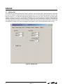
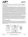
3. User Interface
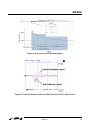
The default FCS GUIs are shown in Figures 1 and 2. The Bode Plot GUI of Figure 1 illustrates the closed-loop
magnitude and phase response for the Si8250-based buck converter. This GUI displays the response plots with
loop bandwidth, and gain and phase margin data in real time, and includes a cursor function to facilitate plot
measurement at any point. The Real Time Compensation data entry GUI shown in Figure 2 consists of multiple
user interfaces, each with its own selection tab (the Setup GUI is shown). The user specifies power stage and
controller parameters using this set of GUIs. (For example: power stage parameters such as output filter L and C
values; Si8250 control parameters such as ADC LSB size and sampling frequency, PWM frequency, etc).
Figure 1. Default Bode Plot GUI
Rev. 0.1 7/06
Copyright © 2006 by Silicon Laboratories
AN294
AN294
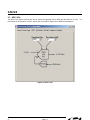
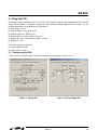
3.1. Setup GUI
The Setup GUI of Figure 2 allows the user to specify the top-level configuration of the system to be simulated. The
Power Stage block represents the power circuits of a single or multiphase buck converter. The Delay block
represents the unit delay (nS) through the power stages due to driver propagation delay and other factors. The
Gain block (immediately following the Delay block) represents additional gain due to an external amplifier or other
gain source. Each of these three blocks can be included in the simulation by "checking" (left mouse button click)
the associated selection box. The remaining blocks in this GUI are related to the Si8250 digital controller. The
selection shown in Figure 2 is typical, and consists of the ADC, PID and 2-pole low-pass filter, and DPWM
modulator. The user can select any combination of blocks to be included (or excluded) from the simulation.
Figure 2. Default Setup GUI
AN294
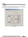
3.2. Power Stage GUI
The Power Stage GUI (Figure 3) shows a single-phase buck topology. The user enters values for the converter
input voltage (Vin), the filter components (inductor and associated series resistance, capacitor and associated
series resistance), and the output load resistance value. The up/down buttons associated with each field allow the
user to increment or decrement the specified values by simply clicking on the appropriate button. As with all other
GUIs in this tool, the specified values may also be changed by simply typing over them, then pressing the ENTER
key. Although a single-phase schematic is shown, a multiphase circuit can be modeled by adjusting only the
inductor parameters. For instance, an equivalent two-phase design would include two equally sized inductors
whose values are one-half that of a single-phase design. To model this, both the inductor's DCR and L values need
to be adjusted accordingly. All other parameters in the model remain the same.
Figure 3. Power Stage GUI
AN294
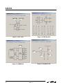
3.3. ADC1 GUI
The ADC1 GUI (Figure 4) allows the user to specify the sampling rate (in MHz) and the LSB size (in mV).
information on the operation of ADC1, please refer to the ADC1 chapter of the Si8250 Users Manual.
Figure 4. ADC1 GUI
For
AN294
3.4. PID/Filter GUI
The PID/Filter GUI (GUI) contains a group of slider controls allowing adjustment of the Si8250 loop compensation
filter coefficients. (For more details on these parameters, please see the "DSP Filter Engine" chapter of the Si825x
User Manual.) The default values in this GUI are for the Silicon Laboratories single-phase POL reference design,
which is detailed in the "Appendix—Single-phase POL Reference Design Specifications" on page 17 of this
document. After editing the power stage parameters to match the system to be simulated, the user typically
maintains the default filter coefficient values as a starting point, and adjusts the sliders one at a time while
observing the response on the Bode Plot display GUI until the desired frequency response is achieved. An
example design exercise appears in "5. Using the FCS" on page 11.
Figure 5. PID/Filter GUI
AN294
3.5. DPWM GUI
The Si8250 contains a digital PWM modulator (DPWM) the output of which moves in discrete time steps. The
maximum number of time steps for any given switching cycle is 511. The SW_CYC field in the DPWM GUI
(Figure 6) allows the user to specify the number of DPWM time steps per switching cycle. (For more information on
DPWM operation, please see the DPWM chapter of the Si8250 Users Manual.)
Figure 6. DPWM GUI
AN294
3.6. Feedback GUI
The Feedback GUI (Figure 7) allows the user to specify values for the feedback divider resistors, and the
capacitance seen by the resulting feedback voltage (which will typically include the anti-aliasing capacitor required
for ADC1). The user must also specify any external gain (such as an external amplifier) and the power stage group
delay (propagation delay of the gate drivers plus turn-on delay of the transistors, plus other external sources of
delay) for maximum simulation accuracy.
Figure 7. Feedback GUI
AN294
3.7. Utilities GUI
The Utilities GUI (Figure 8) provides the means to adjust the scale of the frequency plots that appear in the Bode
Plot GUI. For instance, modifying the Gain Plot Scale button from 1 to 2 increases the amplitude of the plot in the
Bode Plot GUI by 2. The Gain Plot Offset button shifts the Gain Plot up or down. This can be very useful when
skewing sections of the plot for more detailed information. The Line Smoothing box eliminates digital sampling
artifacts in the Bode Plot GUI for clearer viewing. The Sensitivity button increases the resolution of the Bode Plot
GUI. When checked, the Enable Trace automatically updates the Freq, Phase, and Gain parameters at the top left
of the Bode Plot display as the mouse is dragged over any portion plot for precise parameter measurement.
Figure 8. Utilities GUI
AN294
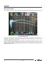
4. Cursors and Zooming
Cursors allow precise gain and phase margin measurements as shown in Figure 9. Gain and phase margin values
at the cursor location are displayed in the upper left of the screen.
Cursors
Figure 9. Using Cursors and Zooming
Zooming provides greater display resolution, and is accomplished by moving the mouse to the top left corner of the
area to be zoomed, then clicking and dragging the mouse to the bottom right corner of the desired zoom area. A
dotted box appears over the zoom area of interest (Figure 10). Once the area is chosen, release the left mouse
button and the area will be zoomed. Note that multiple zooms into an area can be implemented. To return to the
original non-zoomed Bode Plot GUI, click the left mouse button anywhere in the Bode Plot GUI.
AN294
Figure 10. Zooming
AN294
5. Using the FCS
This design example illustrates usage of the FCS, and is based on Silicon Labs' single-phase POL reference
design board (detailed in "Appendix—Single-phase POL Reference Design Specifications" on page 17). The
following parameters are repeated here for convenience:
Input voltage: 12 VDC
Output voltage: 3.3 VDC @ 20 A max
Switching frequency: 380 kHz ±2%
Output inductor: 1 H ±20% (DCR: 1.56 mΩ)
Output caps: 410 F ±20% (Capacitor ESR: 1.25 mΩ)
RDS(on): 2.5 mΩ
The desired frequency response is:
Loop Bandwidth: 35 kHz
Phase margin: 45 deg
5.1. Configuring the GUIs
Launch the FCS and edit the data in each GUI to match the settings shown in Figures 11–16.
Figure 11. Set-up GUI
Figure 12. Power Stage GUI
AN294
Figure 13. ADC1 GUI
Figure 14. PID/Filter GUI
Figure 15. DPWM GUI
Figure 16. Feedback GUI
AN294
The default system configuration is used in the Setup GUI of Figure 11. The values in Figure 12 are given except
for the load value, which is calculated by dividing the nominal output voltage by the full load current (i.e., 3.3 V/
20 A).
ADC1 setup (Figure 13) uses a 4 mV LSB size to avoid limit cycling yet provide adequate measurement sensitivity
(for more information, please see Application Note “AN259: Designing with the Si8250 Digital Power Controller").
The required 35 kHz bandwidth can be met using the lower speed (5 Mhz) clock setting, and provides better pole/
zero control resolution for nonlinear control applications ("Appendix—Single-phase POL Reference Design
Specifications" on page 17 provides an overview of nonlinear control). A calculated ADC1 sampling frequency
value of 4.9 MHz (Figure 13) is calculated by multiplying the 24.5 MHz Si825x master clock frequency and PLL
multiplication factor, then dividing by the ADC1 clock divider ratio (i.e. 24.5 x 106 x 8/40). The default settings for
the PID/Filter (Figure 14) are maintained; it is these settings that will be modified later to achieve the desired
frequency response.
Referring to the DPWM GUI of Figure 15, the SW_CYC value determines the number of discrete DPWM time steps
per switching cycle. Substituting the internal 200 MHz DPWM clock frequency (FDPWM), and the 380 Khz PWM
frequency value into Equation 1 results in a value of 526; the default SW_CYC parameter value of 511 is therefore
maintained.
F DPWM
F switch = ----------------------------------------------SW_CYC[8:0] ÷ 1
Equation 1. DPWM Switching Frequency
The Feedback GUI parameters (Figure 16) are left at their default values as these parameters match the reference
design hardware.
As shown in Figure 17, the values programmed into the FCS for this exercise result in a loop bandwidth of
11,283 Hz with a phase margin (PM) of 38.58 degrees. The parameters in the PID/Filter GUI will be adjusted to
achieve the target response of 35 KHz and 45 degrees phase margin.
Figure 17. Power Stage Effects
AN294
5.2. Filter Coefficients
As configured for this design, the Si825x DSP filter engine has a first-stage PID filter, followed by a second stage
two-pole low pass filter (LPF). The PID filter has three coefficients: kp, ki, and kd. For more information on the
operation of these parameters, please see Application Note “AN259: Designing with the Si825x Digital Power
Controller". A short summary of the changes in frequency response with changes in coefficient values is as follows:
Increasing ki provides more low frequency loop gain but less phase margin.
Increasing kd provides more high frequency, greater loop bandwidth and more phase margin, but increases
output voltage noise.
Increasing kp provides higher loop gain.
The LPF provides two poles and an adjustable output gain. Poles a1, a2 set the corner frequencies of the LPF.
These poles reduce switching noise and help optimize phase margin and loop bandwidth values. Increasing a3
increases loop gain and typically increases phase margin.
5.3. Adjusting Frequency Response
The results of Figure 17 show both loop gain and phase margin below the target values. Increasing loop gain by
increasing the value of a3 will improve both. With a3 now adjusted to 0x66, as shown in Figure 18, the bandwidth
increases to 35,250 KHz and phase margin increases to 49.95 degrees.
AN294
Figure 18. Final Filter Compensation Settings
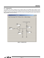
Although Figure 18 shows the frequency response for the entire closed-loop system, other aspects of the
simulation can be observed separately. For example, the open-loop frequency response of just the PID filter can be
observed by simply "unchecking" the other system blocks as shown in Figure 19. The resulting response of only
the PID filter is shown in Figure 20.
AN294
Figure 19. Observing PID Filter Response
Figure 20. PID Filter Response
AN294
APPENDIX—SINGLE-PHASE POL REFERENCE DESIGN SPECIFICATIONS
Introduction
The specifications below summarize the Si825x Single-phase POL Reference Design.
Input voltage: 10–15 VDC
Output voltage: 3.3 VDC @ 20 A max
Switching frequency: 380 kHz ±2%
Output inductor: 1 µH ±20% (DCR: 1.56 mΩ)
Output caps: 410 µF ±20% (Capacitor ESR: 1.25 mΩ)
RDS(on): 2.5 mΩ
Steady-State Bandwidth: ~35 kHz
Steady-State Phase margin: ~ 45 deg
Transient BW: ~100 kHz
Transient PM: ~40 deg
Power efficiency: up to 92%
Line Regulation: 0.42% (15 A load)
Load Regulation: 0.3% (0~18 A load)
Transient Response:
100 mv under/overshoot
20 us recovery time
5–10 A, 2.5 A/µs
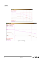
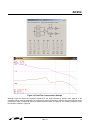
POL Power Efficiency(FW=380 kHz)
0.94
Efficiency
0.92
0.9
0.88
0.86
0.84
0.82
0
5
10
15
20
Output current
Figure 21. Power Efficiency Curve with Load Changing
Note: Under load and over temperature, the output capacitors typically lose 20 percent of their rated value. Therefore, the
nominal 410 µF output caps modeled here can easily drop to 328 µF or less. The FCS can be used to simulate these
and various other effects.
AN294
Non-Linear Control
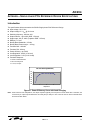
The measured loop frequency response of the Si825x Single-phase POL Reference Design is shown in Figure 22.
Figure 22. POL Loop Frequency Response Measured with Network Analyzer
(12 V Input Voltage at 8 A)
Different filter coefficients are brought into play during system operation, depending on load conditions. The
"steady-state" PID coefficients for the Si825x Single-phase POL reference design are kp = 0x0B, ki = 0x01,
kd = 0x18, a1 = 0xB3, a2 = 0x2E, a3 = 0x28.
A set of "transient response" (nonlinear control) coefficients are automatically enabled at the onset of a load
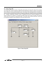
transient. Figure 23 illustrates the algorithm executed by the POL to quickly resolve a transient (for more
information, please see “AN271: Si8250 Real-time Kernel Overview"). Figure 24 shows the response improvement
delivered by nonlinear control.
AN294
Figure 23. Non linear Control Kernel Algorithm
Figure 24. Transient Response with Load Step from 25% to 50%, di/dt 2.5 A/us
AN294
RELEVANT DOCUMENTS
Si825x Data Sheet
Si825x Users Manual
Application Note 259: "Designing with the Si8250 Digital Power Controller"
Application Note 271: "Si8250 Real-time Kernel Overview"
AN294
NOTES:
AN294
CONTACT INFORMATION
Silicon Laboratories Inc.
4635 Boston Lane
Austin, TX 78735
Tel: 1+(512) 416-8500
Fax: 1+(512) 416-9669
Toll Free: 1+(877) 444-3032
Email: [email protected]
Internet: www.silabs.com
The information in this document is believed to be accurate in all respects at the time of publication but is subject to change without notice.
Silicon Laboratories assumes no responsibility for errors and omissions, and disclaims responsibility for any consequences resulting from
the use of information included herein. Additionally, Silicon Laboratories assumes no responsibility for the functioning of undescribed features
or parameters. Silicon Laboratories reserves the right to make changes without further notice. Silicon Laboratories makes no warranty, representation or guarantee regarding the suitability of its products for any particular purpose, nor does Silicon Laboratories assume any liability
arising out of the application or use of any product or circuit, and specifically disclaims any and all liability, including without limitation consequential or incidental damages. Silicon Laboratories products are not designed, intended, or authorized for use in applications intended to
support or sustain life, or for any other application in which the failure of the Silicon Laboratories product could create a situation where personal injury or death may occur. Should Buyer purchase or use Silicon Laboratories products for any such unintended or unauthorized application, Buyer shall indemnify and hold Silicon Laboratories harmless against all claims and damages.
Silicon Laboratories and Silicon Labs are trademarks of Silicon Laboratories Inc.
Other products or brandnames mentioned herein are trademarks or registered trademarks of their respective holders.