1
DVD Micro System
MCD728
all versions
Service Manual
TABLE OF CONTENTS
Handling chip components ............................................................1-1
Information about lead-free soldering ............................................1-2
Technical specification...................................................................2-1
Service tools ..................................................................................2-1
Service measurement setup ..........................................................2-2
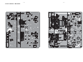
CPU BOARD
circuit diagram ..........................................................................9-1
layout diagram ..........................................................................9-2
Pre-AMP BOARD
circuit diagram ........................................................................10-1
layout diagram ........................................................................10-2
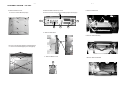
Connections and controls ......................................................3-1...3-4
Disassembly diagram ............................................................4-1...4-2
Software version and upgrading ....................................................5-1
Set block diagram ..........................................................................5-2
Set wiring diagram .........................................................................5-3
VFD BOARD
circuit diagram ..........................................................................6-1
layout diagram ..........................................................................6-2
TUNER BOARD
circuit diagram ......................................................................7-1
layout diagram .......................................................................7-2
DVD MPEG BOARD
circuit diagram ..............................................................13-1...13-5
layout diagram ........................................................................13-6
Exploded view diagram......................................................14-1...14-2
Service partslist .................................................................14-3...14-5
Factory partslist..................................................................15-1...15-5
AMP BOARD
circuit diagram ..........................................................................8-1
layout diagram ..........................................................................8-2
© Copyright
2007 Philips Consumer Electronics B.V. Eindhoven, The Netherlands
CLASS 1
LASER PRODUCT
All rights reserved. No part of this publication may be reproduced, stored in a retrieval
system or transmitted, in any form or by any means, electronic, mechanical, photocopying,
or otherwise without the prior permission of Philips.
Published by DB 0730 Service Audio
Version 1.2
Printed in The Netherlands
Subject to modification
© 3141 785 31692
1-1
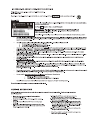
HANDLING CHIP COMPONENTS
1-2
SYSTEM
Total output power .............................................. 400W
Power supply ............................ 220 – 240 V / 50 Hz
Rated working power consumption (1/8 rated
output power) ........................................................ ≤ 85W
AUX input sensitivity ..................................... ≤ 500mV
Channel Separation ............................................. ≥ 40dB
Distortion ....................................................................... 0.7%
Eco power Standby ................................................ < 1W
DVD
Frequency response 100Hz-20kHz (+0.5/-2 dB)
Video output ................................................................ 1 VP-P
HDMI 480p (60Hz), 720p (60Hz), 1080i (60Hz),
576p (50Hz), 720p (50Hz), 1080i (50Hz)
Horizontal definition ................................... 500 (TV)
Dimensions ...............................................................................
....................... 232 (W) x 75.5 (H) x 223.5 (D) mm
Weight .......................................................................... 2.3 kg
AMPLIFIER
Rated output power (THD = 10%) ..........................
........................................ 2x75W (4Ω) + 150W (8Ω)
Frequency response 100Hz-20kHz (+0.5/-2 dB)
S/N Ratio ................................................................... ≥ 60dB
Loaded impedance ..................................................... 4 Ω
Dimensions ...............................................................................
....................... 232 (W) x 75.5 (H) x 223.5 (D) mm
Weight ....................................................................... 4.35 kg
TUNER
FM Frequency range .......................... 87.5-108 MHz
FM Noise limit sensitivity .......................... ≤ 20µ V/M
FM S/N ........................................................................ ≥ 46dB
SPEAKER
Front Speakers
Impedance ........................................................................ 4 Ω
Input power .................................................................. 75W
Sensitivity .............................................................. 80 ± 4dB
Frequency response ................................ 80Hz-16kHz
Dimensions . 150 (W) x 323 (H) x 150 (D) mm
Weight ............................................................... 2.4 kg each
Subwoofer
Subwoofer (not magnetically shielded design).....
................................................................................................ 6.5”
Impedance ........................................................................ 8 Ω
Input power ................................................................ 150W
Dimensions (w x h x d) ....................................................
..................................... 430 mm x 262 mm x 292 mm
Weight ............................................................................ 4.4 kg
REMOTE
Distance ............................................................................... 6m
Angle ............................................................................... ± 300
2-2
IMPORTANT!
– The type plate is located at the bottom
of the system.
– Before connecting the AC power cord to
the wall outlet, ensure that all
other connections have been made.
– Never make or change any connections
with the power switched on.
Subwoofer
Speaker
(right)
2
1
Speaker
(left)
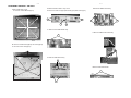
VIEWING AREA
Subwoofer
Front
speaker
( right )
Notes:
– To avoid magnetic interference, do not position
the front speakers too close to your TV set.
– Allow adequate ventilation around the DVD
System.
Place the subwoofer on the floor near the TV.
Place the front left and right speakers at equal
distances from the TV set and at an angle of
approximately 45 degrees from the listening
position.
Front
speaker
( left )
Step 1: Placing the speakers
and subwoofer
FM
antenna
AC Power
2
1
Notes:
– Ensure that the speaker cables are correctly
connected. Improper connections may damage the
system due to short-circuit.
– For optimal sound performance, use the
supplied speakers.
– Do not connect more than one speaker to any
one pair of +/- speaker jacks.
– Do not connect speakers with an impedance
lower than the speakers supplied. Please refer to
the SPECIFICATIONS section of this manual.
Connect the passive subwoofer to the
SUBWOOFER (8Ω) terminal with the
supplied subwoofer cable by matching the plug
types.
Connect the speaker wires to the SPEAKERS
terminals, right speaker to FRONT (4Ω) R and
left speaker to FRONT (4Ω) L. Fully insert the
connectors on the cables into the terminals and
fasten the hooks to ensure firm connection.
Step 2: Connecting speakers
VIDEO IN
S-VIDEO
IN
TV IN
AUDIO
IN
VIDEO IN
S-VIDEO
IN
TV IN
Note:
– Ensure that the “TV” indication on SCART cable
is connected to the TV set and “DVD” indication on
SCART cable is connected to the DVD Player.
● Use the SCART cable (black) to connect the
DVD Player’s SCART jack to the corresponding
Scart input jacks on the TV (cable not supplied).
AUDIO
IN
Using SCART jack
IMPORTANT!
– You only need to make one video
connection from the following options,
depending on the capabilities of your TV.
– Connect the DVD system directly to
the TV.
– A SCART connection allows you to
use features both Audio and Video
features on the DVD Player.
Step 4: Connecting TV
● Connect the serial port marked “CONTROL
CABLE” at the rear of the DVD player to the
same port at the rear of the power amplifier
with the supplied flat control cable.
Step 3: Connecting the control
cable
3-1
CONNECTION AND CONTROLS
2
1
To listen to the TV channels through this DVD
system, use the audio cables (white/red-not
supplied) to connect AUX IN L/R jacks to the
corresponding AUDIO OUT jacks on the TV.
Use the composite video cable (yellow) to
connect the system's VIDEO jack to the video
input jack (or labelled as A/V In, Video In,
Composite or Baseband) on the TV set.
Using Composite Video jack
3
2
1
Note:
– If your TV does not support Progressive Scan,
you will not be able to view the picture.
Press SYSTEM MENU on the remote to exit the
system menu and then DISC and “1” to exit
progressive scan.
If you are using a Progressive Scan TV (TV must
indicate Progressive Scan or ProScan capability),
to activate TV Progressive Scan, please refer to
your TV user manual. For DVD system
Progressive Scan function, see “Getting StartedSetting up Progressive Scan feature”.
To listen to the TV channels through this DVD
system, use the audio cables (white/red-not
supplied) to connect AUX IN L/R jacks to the
corresponding AUDIO OUT jacks on the TV.
Use component video cables (red/blue/green not supplied) to connect the DVD system's
COMPONENT (Pr/Cr Pb/Cb Y) jacks to
the corresponding Component video input jacks
(or labeled as Y Pb/Cb Pr/Cr or YUV) on the TV.
IMPORTANT!
– The progressive scan video quality is
only possible when using Y Pb Pr, and a
progressive scan TV is required.
Using Component Video jacks (Y Pb Pr)
2
1
To listen to the TV channels through this DVD
system, use the audio cables (white/red-not
supplied) to connect AUX IN L/R jacks to the
corresponding AUDIO OUT jacks on the TV.
Use an S-Video cable (not supplied) to connect
the DVD system’s S-VIDEO jack to the SVideo input jack (or labeled as Y/C or S-VHS) on
the TV.
IMPORTANT!
– If S-Video is used for DVD playback
connection, the system’s VIDEO OUT
setting will need to be changed
accordingly.
Using S-Video jack
3
2
1
Use the composite video cable (yellow) to
connect the DVD system’s VIDEO jack to the
video input jack on the RF modulator.
Use an RF coaxial cable (not supplied) to
connect ANTENNA OUT or TO TV jack on the
RF modulator to the Antenna IN jack on the TV.
Connect the Antenna or Cable TV service signal
to the ANTENNA IN or RF IN jack on the RF
modulator. (It may have been connected to your
TV previously. Disconnect it from the TV.)
IMPORTANT!
– If your TV only has a single Antenna In
jack (labeled as 75 ohm or RF In), you
will need an RF modulator in order to
view DVD playback on the TV. See your
electronics retailer or contact Philips for
details on RF modulator availability and
operations.
Using an accessory RF modulator
3-2
CONNECTION AND CONTROLS
1
Note:
– Adjust the position of the antennas for optimal
reception.
– Position the antennas as far as possible from
your TV,VCR or other radiation source to prevent
unwanted interference.
Connect the supplied FM antenna to the FM (75
Ω) jack. Extend the FM antenna and fix its end to
the wall.
For better FM stereo reception, connect an
external FM antenna (not supplied).
Step 5: Connecting FM antenna
IMPORTANT!
– Some discs are copy-protected.You
cannot record the disc through a VCR or
digital recording device.
– When making connections, make sure
the colour of cables matches the colour
of jacks.
– Always refer to the owner’s manual of
the other equipment for complete
connection and usage details.
Additional: Connecting
additional equipment
Never make or change any connection with the
power switched on.
After everything is connected properly,
plug in the AC power cord to the power
outlet.
Step 6: Connecting the power
cord
● Connect the DVD micro system's
SUBWOOFER jack to the AUDIO INPUT
jack on an active subwoofer (not supplied).
Connecting an active subwoofer D
● Connect the system's COAXIAL or
OPTICAL jack to the DIGITAL IN jack on a
digital recording device.
Before star ting operation, set the DIGITAL OUT
according to the audio connection. (See
"DIGITAL OUT".)
Recording (digital) C
● Connect one of the system's VIDEO jack to the
corresponding VIDEO IN jack and AUDIO
OUT L/R jacks to the AUDIO IN jacks on the
VCR. This will allow you to make analogue stereo
(two channel, right and left) recordings.
Using the VCR for recording DVDs B
● Connect the system's AUX IN L/R jacks to the
AUDIO OUT jacks on the other audio/visual
device (such as a TV, VCR, Laser Disc player or
cassette deck).
Before starting operation, press SOURCE on
the front panel to select AUX or press AUX on
the remote in order to activate the input source.
Viewing and listening to the playback of
other equipment A
HDMI IN
E
Notes:
– Proceed to "Setup Menu Options" ➜ "VIDEO
SETUP PAGE" ➜ "HDMI SETUP" for detailed
HDMI setup.
– If you are using the HDMI as audio source
make sure that "DIGITAL OUTPUT" is set to "PCM
only" (see "Setup Menu Options" ➜ "AUDIO
SETUP PAGE" ➜ "DIGITAL AUDIO SETUP").
– To stop sound output from your TV after
making the HDMI connection, make sure that
"DIGITAL OUTPUT" is set to "SPDIF OFF" (see
"Setup Menu Options" ➜ "AUDIO SETUP PAGE"
➜ "DIGITAL AUDIO SETUP").
HDMI IN
HDTV
● Use a HDMI cable (not supplied) to connect the
HDMI jack on the DVD Player to HDMI IN
on a HDMI compatible device (e.g.; TV, Projector,
Adaptor).
➜ It may take a while for the DVD player and
input device to communicate and initialise.
➜ Playback starts automatically.
It has plug and play capability using only one
cable for both audio/video output.
HDMI connects untouched and uncompressed
digital transmission for the highest and crispest
sound/image quality.
Connecting to a TV with HDMI Jack E
3-3
CONNECTION AND CONTROLS
0
switches on the system or puts it on to Eco
power/normal standby mode.
shows the current status of the DVD player.
starts or interrupts disc playback.
in tuner mode, selects a preset radio station
forward.
stops disc playback or erases a program.
in tuner mode, selects a preset radio station
backward.
in Demo mode (on the system only), activates/
deactivates the demonstration.
–
enables/disables the surround sound effect with
moving speakers.
6 MOVING SURROUND
–
–
–
5 PRESET-/9
–
4 PRESET +
–
3 ÉÅ
–
2 Display
–
1 ECO POWER/STANDBY-ON y
DVD player and power amplifier
9
1
2
Tuner:
tunes to a higher/lower radio frequency.
press and hold, then release the key to
start automatic search for a radio frequency
downward/upward.
opens or closes the disc tray.
switches the system on.
selects the respective sound source: DVD/AUX/
TUNER.
switches the system on.
IR SENSOR
point the remote control towards this sensor.
–
–
–
adjusts the volume upward/downward.
adjusts the hours and minutes in clock/timer
setting mode.
switches the set timer ON or OFF.
! VOLUME -/+
–
0
–
–
9 SOURCE
–
–
8 OPEN•CLOSE ç
–
–
–
Disc:
skips to the previous/next chapter/title/track.
7 ¡/™
!
8 56
734 7
switches on the system or puts it on to Eco
power/normal standby mode.
–
selects the respective sound source for DVD/
AUX/TUNER.
exits P-SCAN (progressive scan). (Only for
DISC)
displays information on TV screen during
playback
mode for a disc.
repeats playback of a specific section on a disc.
(
*
&
≥
ª
%
$
#
)
¡
™
£
≤
^
§
∞
•
⁄
º
–
@
!
9 SYSTEM MENU (disc mode only)
8
7
0
5
6
9
enters or exits the system menu.
selects different slow playback modes for a
DivX/VCD/SVCD/DVD.
or off .
DVD/VCD: enters or exits the disc contents
menu.
selects an item in a menu.
moves an enlarged picture up/down/left/right.
(2 / 1; Tuner) tunes to a higher/lower radio
frequency.
(2 / 1; Tuner) press and hold, then release the
key to start automatic search for a radio
frequency downward/upward.
(2 / 1; Disc) searches backward/forward in a
disc at different speeds.
–
confirms a selection.
@ OK
–
–
–
–
–
!4 / 3 / 2 / 1
–
–
–
0 DISC MENU (disc mode only)
–
8 SLOW
4
3
selects different levels of brightness for the
display screen.
2
–
7 DIM
–
6 A-B
–
5 MODE
–
4 DISPLAY
–
–
3 DISC/TUNER/AUX
1
opens or closes the disc compartment
20
–
1 STANDBY B
Remote control
3-4
CONNECTION AND CONTROLS
DVD/VCD/Picture CD: enlarges or reduces a
picture or active image on the TV screen.
Disc: skips to the previous/next chapter/title/
track
Tuner: selects a preset radio station.
starts or interrupts disc playback.
stops disc playback or erases a program.
enables or disables automatic loudness
adjustment.
inputs a track/title/chapter number of the disc.
to select the desired DBB level (DBB 1, DBB 2
or DBB OFF).
selects different types of preset sound equalizer
settings (FLAT, POPS, JAZZ, CLASSIC or
ROCK).
adjusts the volume upward/downward.
adjusts the hours and minutes in clock/timer
setting mode.
switches the set timer ON or OFF.
selects a DVD camera angle.
for DVD
selects an audio language.
for VCD/DivX
sets Stereo, Mono-Left or Mono-Right sound
mode.
selects a subtitle language.
–
–
Power-on mode
sets the sleep timer function (auto off).
Standby mode
sets time for switching on the system
automatically.
≤ SLEEP/TIMER
–
£ SUBTITLE
–
–
™ AUDIO
–
¡ ANGLE
–
enables/disables the surround sound effect with
moving speakers.
–
Notes for remote control:
– First, select the source you wish to
control by pressing one of the source select
keys on the remote control (DISC or
TUNER, for example).
– Then select the desired function ( 2;, í,
ë for example).
for tuner, displays RDS information.
⁄ RDS
–
º MOVING SURROUND
Disc: fast searches in a disc by entering a time,
title, chapter or track.
FM: sets stereo or mono sound mode.
–
disables or enables sound output.
ª MUTE
–
–
–
• VOLUME +/-
–
≥ DSC
–
–
DVD/VCD/CD: enters the program menu.
MP3/WMA-CD: adds/deletes a programmed
track to/from the program list.
Tuner: programs preset radio stations.
Eco power mode
displays the system clock and switches to the
standby mode.
Playback mode
displays the system clock.
Standby mode
sets the system clock.
§ DBB
–
–
–
∞ CLOCK
) GOTO/STEREO
–
–
–
( PROGRAM
–
* Numeric Keypad (0-9)
–
& LOUDNESS
–
^9
–
% ÉÅ
–
–
$ ¡/™
–
# ZOOM
Functional Overview
3-5
CONNECTION AND CONTROLS
4-1
4-1
DISASSEMBLY DIAGRAM - DVD PART
D.Remove Back Panel & Top cover
D*remove screws T3x4(5pcs)and T3x6(5pcs)and T3x10(2pc)
A.Remove Bottom Cover
A1.remove screws M2.5x4(10pcs)
H.Remove Slid Plank
D1
H
D1
D1
D2
D2
D3
E. Remove DVD Rom
I.Remove VFD board assy
E
B*.remove screws M3x10(8pcs) and M3x8(3pcs)
C*.remove screws M3x8(4pcs) and T3x4(2pcs)
I
C1
F. Remove MOTO cover
C2
I.Remove Side metal Plate
F
B1
J
4-2
4-2
DISASSEMBLY DIAGRAM - AMP PART
A.Remove Bottom Cover
A1.remove screws M2.5x4(8pcs)
G.Remove SMPS board assy
D.Remove Back Panel & Top Cover
D*remove screws T3x4(4pcs)and T3x6(1pcs)and T3x10(1pcs)
D1
D1
G
D3
G
D2
A
E. Remove Pre-AMP Board Assy
H.Remove AMP Front board assy
E
B*.remove screws M3x10(6pcs) and T3x10(4pcs)
C*.remove screws T3x4(5pcs)
H
C
F. Remove AMP Board Assy
F
I.Remove Side metal Plate
B1
I
B2
F
5-1
5-1
SOFTWARE VERSION AND UPGRADING
! "
# $
% #
0 2
$
)3
(
3
$ $
%
.
"
# "
"
*.
&
ǃ#
ǃ"
$
ǃ
&
&
#
)
'
$
$
(
)
$
4
'5
$
.
6
(
$
3
$ $
%
;
(
$
(
)
*
+
'
,
&
'
" (
)* +!
,
"
# $
&
"
- " #
"
-%
7
%
#
&
., /
0
1
"
0
%
6
&
7 & #
#
&
#
"
&
-
#
' 3 " &
:
,
*
%
&
955
&#
$ $
(
+
-5
$ 3
'5
*
(
-
$
&
,
3
2
&#
"
&
$
3
%
$ )
'5
1
(
"!
8
0
$ 3
(
! hh
8, /
3
*
2
34 5 4.
&
)
$ $
!"####
$$%
$
*.
&
,
$ 9
(
$ 9
):
(
):
$
5-2
SET BLOCK DIAGRAM
5-2
5-3
5-3
SET WIRING DIAGRAM
SCART PCB
Pre-AMP BOARD
CPU BOARD
DVD MPEG BOARD
AMP BOARD
POWER BOARD
VFD BOARD
TUNER BOARD
6-1
6-1
CIRCUIT DIAGRAM - VFD BOARD
VFD701
R603
2.2/0.5
NE-1300CD-3.G
C603
104P
C608
334P
3
2
1
CN601
2.0/3P
1
2
3
4
5
6
7
8
9
10
11
12
13
14
15
16
17
18
19
20
21
22
23
24
25
26
27
28
29
30
31
32
33
34
35
36
VF1
VF1
S1
S2
S3
S4
S5
S6
S7
S8
G1
G2
G3
G4
G5
G6
NC
NC
NC
NC
G7
G8
G9
G10
G11
G12
S9
S10
S11
S12
S13
S14
S15
S16
VF2
VF2
C607
334P
VF2-1
VF1-1
-28V
R604
2.2/0.5
C605
104P
S1
S2
S3
S4
S5
S6
S7
S8
G1
G2
G3
G4
G5
G6
G11
G12
S16
S15
S14
S13
-24V
STB1
DATA
CLK
V-GND
+5VS
R602 47K
STADBY
C601
S12/KS12
S11/KS11
S10/KS10
S9/KS9
S8/KS8
S7/KS7
S6/KS6
S5/KS5
S4/KS4
S3/KS3
S2/KS2
S1/KS1
Vdd
26
25
24
23
22
21
20
19
18
17
16
15
14
S12
S11
S10
S9
S8
S7
S6
S5
S4
S3
S2
S1
R605
33K
CLK
STB1
DATA
1
2
3
4
5
6
7
8
9
10
11
12
13
+5VS
S2
4148
D603
S3
D601
S1
KS2
4148
4148
SW601
TACT(STBY)
+5VS
K4
K3
K2
K1
47uF
C602
104P
SW602
D602
KS3
R609 10K
R601 4K7
R610 10K
G5
G4
G3
G2
G1
Vdd
IC601
LED5
uPD16311
LED4(BBE)
LED3(POWER)
LED2(FANCT)
LED1(7507RST)
Vss
OSC
R606 33K
R607 33K
R608 33K
R613
1K LED601
G6
G7
G8
S20/G9
S19/G10
VEE
Vdd
S18/G11
S17/G12
S16
S15
S14
S13
39
38
37
36
35
34
33
32
31
30
29
28
27
G6
G7
G8
G9
G10
CAP±20%,
special parts nated beside parts
protect material licf regulate by green envionment management
SW1
SW2
SW3
SW4
DOUT
DIN
IC
CLK
STB
KEY1
KEY2
KEY3
KEY4
40
41
42
43
44
45
46
47
48
49
50
51
52
RES±10%
All parts comply with suppliey environment
C604 104P
G1
G2
G3
G4
G5
note: tolerance
C610
334P
G7
G8
G9
G10
G11
G12
S9
S10
S11
S12
S13
S14
S15
S16
C609
334P
SW603
1
2
3
4
5
CN602
2.0/6P
K1
TACT(NEXT)
K1
K2
K3
K4
KS3
KS2
SW604
TACT(OPEN/CLOSE)
SW605
K2
TACT(PRE)
SW606
TACT(STOP/BAND)
SW607
K3
TACT(CH+)
SW608
K4
KS3
KS2
TACT(CH-)
Title
TACT(PLAY/PRESET)
6-2
LAYOUT DIAGRAM - VFD BOARD
6-2
7-1
7-1
CIRCUIT DIAGRAM - TUNER BOARD
000
R40
C26
474
C21
1uF
C20
102
0
1
3
3
1
2
34
35
VSTABB
FM-IF2
36
AM-IF2
37
38
AM/FM
VSTABA
40
39
AM-MIXOUT
41
AM-IF1-IN
FM-IF1-IN
R21
470
150K
C15
X1
23
7.8V
C7
C31
104
C32
15pF
470n
C30
2.2uF
VCC2
VCC2
C23
224
C28
1uF
3
4
MPX
R28
820
R29
820
C33
82pF
1
T7
6295
DISCRIMINATOR
C42
224
C43
C39
153
22n-USA
C40
153
22n-USA
VDD
VCC
2
6
VCC2
R41
100
C41
100uF
R17
1M
Q1
9014
R46
1K
R7
330
R37
0
8.2V
R43
4.7K
8.2V
C24
1M
C25
R47
1K
Q3
BC547C
150
Q2
BC857B
+FM
R16
R33
4K7
R30
C29
1uF
Q5
9014
224
120
11V
8.9V
R42
4.7K
120
C34
223
C5
104
C27
474
R4
1
2
3
4
4P
C17 C18
221 221
VCC
RIGHT
SGND
LEFT
R3
CN1
R23
470
C16
221
VDD
VCC1
C19
222
12P
75K
24
ENABLE/MPX
DATA
CLOCK
ST/NO
470
R22
C14102
R14
25
22
FSI
AFC+
28
26
VDD
21
R27
2K2
331
R18
22K
R34
47K
384
J3
000
R45
000
R44
000
VCC
P0
29
DZ1
J2
20
MPX-IN
P1
27
MO/ST
AFC-
11
C6
VCC
RF-GND2
AF-OUT
224
2P
43
XTAL
19
C22
2
1
10
VCO
FMDEM
56K
DGND
IF-GND
100K
9
TUNE
18
R11
CLOCK
PILFIL
CN3
RV1
DATA
Vcc1
16
1
42
2
8
TUNER1
NC
AM-OSC
7
VCC1
WRITE-EN
RIGHT
C9
100uF
2
31
30
P0
FM-OSC
6
32
AM-AFC
P1
15
C3
104
33
FM-IF2-IN
RF-GND1
5
+FM
IC1
TEA5762
FM-GND
4
LEFT
000
AM-RF
3
MUTE
AM ANT
104
RIPPLE
LPF
AM RF GND
3
R9
1
2
14
C13
103
2.2K
C8
44
GND
GND
9
C10
12
FM ANT
C4
104
10
B+
GND
VT
5
6
GND
4
3
2
GND
FM RF GND
4
CF2
10.7M
AM/FM
10uF
100uF
R8
CF1
10.7M
C1
R6
330
2
1
2P
JACK1
CF4
10.7M
17
8
OSC-OUT
T104 R2
120
R5
330
2
120
FM FRONTEND
CN4
R1
7
IF-OUT
AGC
ANT
13
1
1
TUNE1
KST-F404
3
C2
104
R35
22
C35
R31
68K
22uF
R32
10K
224
224
R25
47K
R24
47K
AM/FM
MPX
CN2
1
2
3
4
5
5P
7-2
LAYOUT DIAGRAM - TUNER BOARD
7-2
8-1
8-1
CIRCUIT DIAGRAM - AMP BOARD
R313
+12V
R307
DZ300
5.6K
5.1V
C352
104
C353
104
Vddp2
Vssp2
VssA2
VddA2
C314
102
C315
102
C316
102
+12V R337
100
4001
R334
D301
100
-28V
R333
8.2K
C394
104P
R302
10K
17
14
6
7
VSSP1
VDDP1
MODE
OSC
VDDA1
C360
104
C392
473M
1
2
R338
240K
R335
C318
102
L306
10
C384
470uf/35v
1
2
SW-OUT+
R321
22
R329
10
C378
334(M)
20
104/100V
C362
104
C389
224
C319
102
L302
C368
23
18
C361
104
21
C320
102
C321
102
C332
220P
C333
220P
Vssp3
C322
102
+28V
JRH0349
C385
470uf/35v
L307
10 R328
JRH0349
-28V
-28V
+28V
-28V
3.3K
C393
104p
IC302
TL072
R336
C355
3.3K
+28V
C395
104p
220uf
CLOCK PD1
10UH
+28V
L308
R345
C1
104
100UF/16V
1K
DZ5001
5.6V
IC303
C3
104
C2
1
2
R346
3
6.8K
4
5
R348
1M
C7
C5
101
XT301
700K
33P
C6
101
R347
10K
6
7
I1
IC304
Vcc
O1
I6
I2
O6
O2
I5
I3
O5
O3
I4
GND
PC74HCU04D
O4
14
13
12
11
10
9
8
1
C4
104
Q1
VDD
14
C9
104
2
C8
100p
3
R349
22
4
5
6
7
Q1
Q2
C1
Q2
R1
C2
D1
R2
S1
D2
VSS
S2
HEF4013T
2p/2.5
27uH
C372
153
VSSP2
VDDP2
STABL
VSSD
SUB/VSSD
C374
153
OUT2
SW-OUT-
22
C381
22uf/100V
474
C354
+VsOUT1
9P/2.5
BOOT2
15
C351
104
R319
22
L301
27uH
C371
153
R327
FAN
C398
220uf
OUT2IN1-
R332
8.2K
1
2
2.5/2P
C391
473M
C390
334M
CN302
C396
220uF
8
JRH0349
D300
4001
7
10 R325
SR-OUT
C387
1000uf/35v
4
L305
+28V
C386
1000uf/35v
C359
104
C317
102
3
C383
470uf/35v
TDA8920BTH
C376
334(M)
16
1N2+
IN2-
C328
220P
R323
10
Vddp3
IN2- IN1+
JRH0349
C380
22uf/100V
SGND2
Vssp2
IN2+ -Vs
FL IN
FR IN
GND
MUTE
+12V
DGND
-28V
+28V
BOOT1
24
C358
104
6
9
8
7
6
5
4
3
2
1
OUT1
IN1-
C331
220P
5
C382
470uf/35v
CN301
12
10
C377
334(M)
SL-OUT
L304
4
R320
22
R324
10
5
220P
104/100V
SGND1
2
SR-OUT
C330
220P
C357
104
11
R309
5.6K
spart
C350
104
C366
19
VSSP2
VDDP2
L303
R326
10
104/100V
9
4p/2.5
CN300
22uH
C367
C388
224
474
C337
Vssp3
C327
IC301
IN1+
VSSA2
VSSP1
VDDP1
MODE
STABL
C370
153
Vddp2
C313
102
1
2
3
4
22
21
R331
47K
SL-OUT
L300
22uH
20
C373
153
C356
104
C308
102
R317
22
8
C326
220P
C309
1
C369
153
C311
102
104
C349
102
VDDA2
14
6
7
OSC
VSSA1
SUB/VSSD
C339
474
OUT2
23
C312
102
IN2-
19
5.6K
4
BOOT2
15
474
C338
5.6K
R308
C345
104
C375
334(M)
16
1N2+
PROT
R?
4.7K
TDA8920BTH
13
104
SGND2
C329
220P
R310
5
BOOT1
3
FL IN
R312
22K
C303
2
SGND1
18
474
R306
5.6K C336
11
VSSD
R305 C335
474
5.6K
OUT1
R322
10
CLOCK
C347
104
C346
104
C325
220P
104/100V
IN1-
24
9
VSSA2
C304
102
IN1+
C323
220P
R311
22K
220P
IC300
1
R300
4.7K
8
VDDA1
474
C334
5.6K
R304
VDDA2
104
FR IN
12
10
C301
C344
104
C365
102
C310
102
Vddp3
Vssp2
C324
104
C343
C305
R318
22
17
C341
104
C340
104
100UF/25V
560
R330
VSSA1
Vddp2
CLOCK
C379
PROT
C307
102
13
R316
C306
22
102
3
C364
10uF
Vddp3
Vssp3
VssA3
VddA3
2.2K
Q300
BC817B
4.7K
SW-OUT
R303
13
12
11
10
9
8
C363
104
CN303
spart
8-2
LAYOUT DIAGRAM - AMP BOARD
8-2
9- 1
9- 1
CIRCUIT DIAGRAM - CPU BOARD
LED201
LED(BLUE)
5P/2.0
CN204
1
LED202
LED(BLUE)
1
LED203
LED(BLUE)
R211
10K
CN17
2P/2.0
LEDCOM
0
R200
Q200
R201
2P/2.0
CN200
2P/2.5
Q203
8050
Q207
8550
100UF/16V
M-UP
D-GND
DVD IR
DVD STB
DVD CLK
DVD DATA
DVD-TMS
RDS-IN
PLLCE
PLLCLK
PLLDATA
X201
R270
2.2K
L200
R205
R206
R208
10K
8
7
6
5
1K
R238
R241
1K
1K
R242
R244
1K
DVD ON
R257
22K
R243
C229
330P
1K
R256
3.3K
4.19MHz
X202
1
2
3
4
C227
2.2UF/10V 5
6
7
8
32.768KHz
C217 C218
30P 30P
C219 C220
30P
30P
C228
560P
QUAL RDCL
RDDA
T57
VREF OSCOUT
MPX OSCIN
OSEL
Vs
GND EXRES
ARI
TM
FILOUT FSEL
4.33MHz
X203
16
15
14
13
12
11
10
9
IC203
TD2579
R224 2.2K
C230
C224
104P
47P
C231
82P
10K
R217
TUN-ON
+12V
4.7K
9P/2.0
TU-R
R235
R252
SCL
SDA
R254
47K
4.7K
TU-L
4P/2.5
CN206
C223
C253 22uF
47uF
272
C251
C252
2.2uF
C250 272
C241
C248 104
C239 2.2uF
C240 2.2uF
R266
C210
300P
C208
300P
+12V
C254
C211
300P
1
470UF/16V
A5V
REF
3
4
TREB_L
AGND
5
6
R IN
TREB-R
8
7
ROUT
LOUD-R
10
9
CD-R
C238 2.2uF
C209
102
DZ201
9V
220
TUNER-R
TUNER-L
2.2uF
11
14
C234
TAPE-R
C236
2.2uF
R261
100K
12
R259
100K
C244 104
4.7K
2
TUN-L
4P/2.0
L1
200UH
C1
470/16V
B1
Q1
8050
IC204
S12V
A5V
34
33
32
31
30
29
28
27
26
25
24
23
22
21
20
19
18
17
16
15
14
13
12
11
10
9
8
7
6
5
4
3
2
1
R264
1K
C243 2.2uF
2.2uF
ECO-POEWR
28
27
26
25
24
23
22
21
104
C249
R263
8K2
C242
R262
8K2
+12V
OUT-L
OUT-R
speak ctrl-STANDBY
-MUTE
ROT-B
ROT-A
REM
KEY
LED
CLK
DATA
DGND
LFOUT
RFOUT
LROUT
RROUT
BOUT_R
BIN_R
BIN-L
BUOT_L
20
19
17
16
15
18
104
104
C246
100P
C247 104
100P
C232
C245
C233
2.2uF
1K
AUX-L
100K R260
RCA-2P
100K R258
1 R246
LOUT
1K
2.2uF
2
AUX-R
LIN
R247
C237
3
TAPE-L
PT2313L
J200
CN208
34P
tolerance RES±10%
CAP±20%,
special parts nated beside parts
All parts comply with suppliey environment
protect material licf regulate by green envionment management
1
2
3
100 R230
100 R231
100 R232
RDS-IN
TUN-R
470UF/16V
C202
104P
VDD
1
2
3
4
5
4148
CD-L
13
Q210
9014
R236
LOUD_L
R234
4.7K
CN207
R253
47K
CD-L
R245
1K
D-MUTE
CD-R
1
2
3
4
R248
D202
R251
4.7K
MUTE
CN203
SUR-MUTE
speak ctrl
STANDBY
MUTE
DVD-ON
R209
10K
note:
10K
R207
C-20
C-19
C-18
10K
10K
R250
10K
Q209
9015
47K
1
2
3
4
5
6
1
2
3
4
ST/TUNED
PLLCLK
PLLDATA
PLLCE
1
2
3
4
5
1
2
3
VF2
VF1
-27
1
2
3
4
C-20
C-19
C-18
C-44
R216
10K
C258
470P
470
A5V
IC210
2SC9228
R204
22
21
20
19
18
17
16
15
14
13
12
PLL-CL
PLL-DA
RDS-Q
RDS-SDA
RDS-SCL
DVD-STB
DVD-CLK
DVD-DI
DVD-DO
DVD-ON
RESET
R240
1K
C257
470P
R222
R202
10K
speak ctrl
M-DOWN
OPEN-SW
CLOSE-SW
R269
2.2K
8550
C200
10K
8050
1K
R239
Q204
8050
470
R223
C216
103P
LED
M-UP
M-DOWN
DS-STB1
DS-DAT
DS-CLK
REMTOE
ROT-A
ROT-B
M+
M-
C-44
LED
D200
4148
Q208
10K
10K
34
35
36
37
38
39
40
41
42
43
44
C225
104P
LED206
LED(BLUE)
2
1
M+
M-
2
1
C215
103P
IC209
1
2
3
4
R203 10K
ROT-B
ROT-A
REM
KEY
LED
1
S12V
LED205
LED(BLUE)
1
2
3
4
5
6
7
R213
10K
A5V
CN205
1
2
STANDBY
MUTE
SWST/TUNED
ECO-POEWR
SDA
SCL
TUN-ON
R212
10K
LED204
LED(BLUE)
R226 100
R214
R215
A5V
A5V
AC6811
100
R225
330P
LED
M-UP
M-DOWN
DS-STB1
DS-DAT
DS-CLK
REM
ROT-A
ROT-B
1
2
C204
R237
68K
10K
KEY
OPEN-SW
D-GND
CLOSE-SW
C235
2
C203
330P
R265
1K
2
M-OPEN
A5V
R210
10K
5
4
3
2
1
R221
R268 1K
C256
2.2K
470P
470
Q206
C201
8550
220UF/16V
4.7K
R233
D203
4148
1
2
Q201
8050
R219
M-CLOSE
M-OPEN
REM
4
3
2
1
SDA GND
SCL
A2
TEST
A1
Vdd
A0
C222
104P
C226
10UF/10V
PCF8563
M-CLOSE
R267 1K
C255
2.2K
470P
5
6
7
8
C221
47UF/10V
SDA
5
Vss SDA
R220
470
Q205
8550
100UH
SCL
6
SCL
Q202
8050
R218
M1+
M1-
2
R24910K
D204
IN60
IC200
33
32
31
30
29
28 D201
27 4148
26
25
24
23
4
15P
Int
A5V
7
oscO Clk
8P/2.0
CN202
24C01
M-OPEN
M-CLOSE
STANDBY
MUTE
SUR-MUTE
4052-A
ST/TUNED
SDA
SCL
TUN-ON
PLL-CE
3
C212
8
oscI Vdd
CN210
5P/2.0
CN201
7P/2.0
OPEN-SW
KEY
DVD-TMS
CLOSE-SW
Vdd
Vss
XT-OUT
XT-IN
TEST
X-IN
X-OUT
1
2
CN2
3P/2.0
1
2
3
4
5
6
7
8
9
10
11
X200
32.768
U200
CN11
5P/2.0
A5V
D-GND
DS-CLK
DS-DAT
DS-STB1
4001 D205
+12V
D-GND
1
2
CN12
2P/2.0
ECO
D1
4148
R1
C4
473M
1K
Q2
8050
1K
R5
C3
104
VF1
7
VF2
9
4
D2
FR104
5
100
6
R3
100
2
3
R2
R6
22K
1
10
BZ1
R4
100
-27
C2
220U/35V
DZ1
3V
9-2
LAYOUT DIAGRAM - CPU BOARD
9-2
10 - 1
10 - 1
CIRCUIT DIAGRAM - Pre-AMP BOARD
1
2
3
4
5
6
7
8
9
10
11
12
13
14
15
16
17
18
19
20
21
22
23
24
25
26
27
28
29
30
31
32
33
34
CN113
34P
ECO
FR-OUT
FL-OUT
MUTE
LED
R102
8P
4.7K
CN112
1
2
3
4
5
S12V
D-GND
+5V
D-GND
STANDBY
C119
R101
103P
47K
4.7UF
4.7UF
10K
8050
R117
1
2
1
2
2P
C901
Q100
C902
100UF
DZ901
104P
R112
270
5.1V
CN107
2P/2.54
CN501
R901
S1
3
10K
Vcc
GND
REM
2
1
REMOTE
3
2
1
R114
SW901
SOURCE
CN1201
C107
100UF/16V
4.7K
7P
CN108
3P
R104
10K
9014
C100
1
2
3
R902
1.5K
1
2
47K
Q102
R105 1M
ENCODER
R103
C101
+12V
R100
2
1
CN1101
1
2
3
D100
4148
S12V
COM
OUT-SW
ROT-B
ROT-A
D-GND
+5V
+12V
D-GND
REM
KEY
1
2
3
4
5
6
7
8
FL-OUT
CN105
2P/2.0
FR-OUT
CN104
G
B
A
REM-1
GND
12VA
VCC
2.5/8P
CN101
OUT-SW
FL-OUT
FR-OUT
GND
MUTE
+12V
ENCODER301
ROT-A
ROT-B1
1
2
3
4
5
6
+12V
speak ctrl
STANDBY
MUTEROT-B
ROT-A
REM
KEY
LED
+5V
S12V
D101
4148
C102
470uf/16v
+12V
JACK100
3P
2.2
4P
LED1001
R1001
10K
LED
1
2
3
4
2P/2.5
1
2
3
4
JACK101
3P
+12V
speak ctrl
SP-R
SP-L
SP-GND
1
2
3
4
1
2
3
4
+12V
speak ctrl
4P/2.54
SP-GND
CN111
3P
JACK102
note:
tolerance RES±10%
CAP±20%,
special parts nated beside parts
All parts comply with suppliey environment
protect material licf regulate by green envionment management
10 - 2
LAYOUT DIAGRAM - Pre-AMP BOARD
10 - 2
12 - 1
12 - 1
MUTI PCB
B
ASP 12V
G
R
RGB
CVB1
GND
J1201
From dvd decoder
GND21
20.VIDEO IN
19.VIDEO OUT
18.FS GND
17.VIDEO GND
16.FS
15.RED
14.REMOTE GND
13.RED GND
12.REMOTE
11.GREEN
10.CLOCK
9.GREEN GND
8.12V
7.BLUE
6.L-CH IN
5.BLUE GND
4.AUDIO GND
3.L-CH OUT
2.R-CH IN
1.R-CH OUT
SCART-101 (HUAHUI)
检测电压
16:9 ASP=7.5V-8V
4:3 ASP=12V
RGB V/S=3V
VIDEO V/S=0V
R1206 100
ML
R1207 100
MR
R1204 R1205
10K 10K
SCART BOARD
CN1201
10
9
8
7
6
5
4
3
2
1
15P
GND
RGB
ASP 12V
B
G
R
GND
CVB1
ML
MR
13 - 1
13 - 1
CIRCUIT DIAGRAM - DVD MPEG BOARD
MPEG board is not repaired,program for referrence only.
EJS89HD18 MPEG board elements sch
R152
15k
L44
VCC
USBM
USBP
U14
AZ1117H-3.3V/NC
VCC
R153
15k
3
CB75
0.1uF
FB
CB62
0.1uF
IN
2
4
OUT
out
CB63
SOT223
DVDD18
L51
92_DV33
R156
L47
FB
CB71
0.1uF
Y0
Y1
Y2
Y3
Y4
Y5
Y6
Y7
DVDD18
ALRCK
ABCK
ACK
AD0
AD1
AD2
AD3
SPDIF
R
B
AVSS
G
AVDD
AVSS
AVDD
AVSS
FS
VREF
AVDD
80
79
78
77
76
75
74
73
72
71
70
69
68
67
66
65
64
63
62
61
0/NC
R159
DVSS
C0
C1
C2
C3
C4
C5
C6
C7
DVDD33
VCK
DVSS
Y0
Y1
Y2
Y3
Y4
Y5
Y6
Y7
SSCK
SSD
DVDD18
PWDN
RST
CLK
INT
DVSS
A7/GPO0
A6/GPO1
TRAP2/GPO2
TRAP1/GPO3
TRAP0/GPO4
MSCK/GPO5
MSD/GPO6
GPO7
GPO8
GPO9
GPO10
HTPLG
0.1uF
+ CE30
CB69
0.1uF
100uF/16V
TX2-
10k
1k/NC
NC
NC
NC
NC
NC
NC
SWING
AVSS
TX2+
TX2AVDD
TX1+
TX1AVSS
TX0+
TX0AVDD
TCK+
TCKAVSS
AVSS
AVDD
AVDD
PLLC1
PLLC0
AVSS
Differential Signal !
No Through Hole !
100 ohm - Impedance
R157
510
60
59
58
57
56
55
54
53
52
51
50
49
48
47
46
45
44
43
42
41
ESD/NC
92_AVDD3
D7
ESD/NC
Differential Signal !
No Through Hole !
100 ohm - Impedance
TX1+
TX2+
TX2-
TX1-
TX1+
TX1TX0+
TX0-
D8
D9
ESD/NC
ESD/NC
F_TX2+
F_TX2F_TX1+
F_TX1F_TX0+
TXC+
TXC-
F_TX0F_TXC+
TX0+
92PLL_AVDD3
F_TXC-
TX0-
C111 5600pF
D10
D11
ESD/NC
ESD/NC
HDMI_SCL
HDMI_SDA
R160
1.5K
U16
MT1392E HDMI TX PROCESSOR
SPQFP80/SMD
GPO9
GPO10
HPD
U17
1
2
3
4
NC
NC
NC
GND
R161
1.5K
D12
ESD/NC
D13
ESD/NC
HPD
VCC
WP
SCL
SDA
EEPROM 24C16
SO8NB
8
7
6
5
CB74
0.1uF
VCC
D14
D15
ESD/NC
ESD/NC
L49
FB
HDMI_VCC
CB73
0.1uF
R168
1k
R169
1k
MSCK
MSD
1
2
3
4
5
6
7
8
9
10
11
12
13
14
15
16
17
18
19
R162
NC
TXC+
100
100
R164
R165
R166
R167
R170
R171
R172
R173
R174
R175
CB67
FB
Closed to MT1392 Power Pin !
DV33
V601#
H601#
CB72
0.1uF
92_DV33
R154
750/NC
TXCTRAP2
TRAP1
TRAP0
MSCK
MSD
GPO7
NC
FB
XO
L50
DVDD18
R163
FB
INT0#
L48
PWDN#
URST#
92_DV33
0
0.1uF
92PLL_AVDD3
L46
560
92PLL_AVDD3
21
22
23
24
25
26
27
28
29
30
31
32
33
34
35
36
37
38
39
40
XO
R158
CB65
0.1uF
TX2+
SCL
SDA
VCK
CB64
R155
390/NC
D6
1
2
3
4
5
6
7
8
9
10
11
12
13
14
15
16
17
18
19
20
0.1uF
FB
CE29
100uF/16V
C110 0.1uF
CB70
0.1uF
C0
C1
C2
C3
C4
C5
C6
C7
1392_VCK
CB61
0.1uF
YUV4
ACLK
ASPDIF
YUV6
YUV5
92DAC_AVDD3
CB66
0.1uF
SOT223
CB60
0.1uF
92_AVDD3
U15
AZ1117H-ADJ/NC
IN
OUT 2
out 4
1
DVDD18
+
FB
ADJ
3
CB59
92_DV33
0.1uF
L45
V18
CB76
0.1uF
FB
23
22
C109
47uF/16V
FB
33
33
92DAC_AVDD3
L42
+
CE32
47uF/16V
20
21
+
PH-4A
L43
R150
R151
GND
USBVCC
USBUSB+
1
1
2
3
4
92_DV33
DV33
J11
P2
HDMI TYPE-A
HDMI-1
13 - 2
13 - 2
CIRCUIT DIAGRAM - DVD MPEG BOARD
MPEG board is not repaired,program for referrence only.
+5VV
EJS89HD18 MPEG board elements sch
L19
FB
L21 1.8uH
C55
47pF
47pF
L23
FB
R81
SPDIF
22
CVBS_ST
R/V
G/Y
B/U
16:9_SW
R/V_SW
SC
SPDIF
1
VCC
R82
C63
3
C62
47pF
VCC_SPDIF
22
CB53
0.1uF
47pF
+
CVBS
1
2
3
4
5
6
7
8
9
10
11
12
13
P4
AV1-8.4-8D
P3
DSW-03
SC
PH-13A
CE33
47uF/16V
2
1
4
2
C
3
Y
SY
1
G
G
5
47pF
J8
LT
RT
LT
RT
Q12
8550
2
C61
5
1
P1
AV3-8.4-13D
C60
27pF
R80
75/DIP-1/2W
R83
150
4
47pF
+5VV
YUV2
R/V
220uF/16V
ASPDIF
L24 1.8uH
2
3
C56
3
C54
G/Y
B/U
+ CE23
Q11
8550
2
YUV1
R76
150
FB
L20
SY
1
R75
75/DIP-1/2W
+5VV
VCC
R187
470/0805
R84
+5VV
Q13
8550
2
R88
SCART_SW
+5VV
47pF
R87
75
3
CVBS_ST
C66
R86
1k
R89
Q14
2
2N3904
2.2k
C64
C65
47pF
47pF
CE25
2.2k
+
100uF/16V
2N3904
R115
9.1k
R118
10k
R116
33
+12V
R112
75/DIP-1/2W
+ CE26
100uF/16v
SCART_TV
1
L22
Q22
8550
FB
CVBS
DV33
Q16
1 3906 3
R92
C4
47pF
R93
R/V_SW
33
2
3
2
+5VV
4.7K
R95
MUTE
RT
LT
MUTE
RT
LT
J10
CB54
0.1uf
2.2k
mk1
4
3
2
1
mk2
mk3
mk4
PH-4A
y2
RGB_SW
G/Y
Q17
8550
C70
R101
47pF
C79
C80
+5VV
L30
FB
YUV5
R98
150
10k
2
C82
3
1800pF
100k
150pF
+12VA
1
C81
10uF/16V
R104
100
LT
U11A
4558
C71
C73
47pF
47pF
R108
C74
+12V_OUT
Q35
AO3407
R199
10k
1
B/U
10uF/16V
Q18
8550
2
3
L31 1.8uH
R206
R103
5.1k
R102
+
AL
R97
75/DIP-1/2W
22k
+
47pF
4
C69
47pF
8
C67
3
2
+
R96
150
y3
-
YUV4
L27
FB
1
R94
75/DIP-1/2W
L28 1.8uH
R200
100K
R201
20k
22k
C84
47pF
Q36
3904
150pF
standby
R202
R100
150
1
Q19
8550
2
C75
C77
47pF
47pF
3
YUV6
C78
47pF
R/V
10uF/16V
10k
1800pF
7
U11B
4558
VREF
+12V
C116
0.1uF
CB55
0.1uF
C86
10uF/16V
+
4
C87
8
L33
FB
6
5
+
R99
75/DIP-1/2W
R207
100k
10k
R110
5.1k
+
AR
+5VV
R109
-
C85
L34 1.8uH
+12V_OUT
3
R90
150
VREF
Q15
2
1
YUV3
D16
12V
1
L25
FB
1
R85
75/DIP-1/2W
L26 1.8uH
16:9_SW
680
3
+12V_OUT
R111
100
RT
13 - 3
13 - 3
CIRCUIT DIAGRAM - DVD MPEG BOARD
MPEG board is not repaired,program for referrence only.
EJS89HD18 MPEG board elements sch
V1P4
DV33
L12
FB
RFV18
CB23
0.1uF
DV33
L13
L14
L15
ADACVDD
APLLVDD3
DACVDD3
47uH
47uH
FB
+
CE16
JITFO
C46
390pF
C
B
A
D
RFO
RFO
CB24
47uF/16V
CB25
+
0.1uF
CB26
+
0.1uF
1uF
120pF/NC
CB27
CE18
47uF/16V
+
0.1uF
C47
R64
R/NC
DV33
OPO
OPOP+
DMO
FMO
TEZISLV
TRO
FOO
TRO
FOO
C49
5600pF
R65
10k
+
D3
R67
10k
1N4148/NC
FB
USBP
USBM
CB36
0.1uF
URST#
ADIN
USBVDD
ADIN
TMS
TCK
TMS
TCK
V18
Q10
3904
2
14
14
2
U6B
XTALI
10
C25
20pF
7
74HC04
7
R55
4
3
74HC04
2k
0.1uF
U6A
1
R58
100k
27MHz
C32
27pF
DACVDD3
DACVDD3
OUT1
OUT2
OUT3
XO
R59
C31
Y1
APLLVDD3
ASPDIF
PWDN#
ACLK
ASPDIF
PWDN#
MUTE
2.7uH/NC
C24
1000pF/NC
SCART_SW
SCART_TV
RGB_SW
DV33
V18
AR
AL
C30
10uF/10v
AR
AL
ADACVDD
RFV18
JITFN
JITFO
XTALI
0.047uF
C36
PLLVDD3
RFVDD3
C35
0.047uF
C27
C29
1uF
R56
1k
CE13
220uF/16V
ALRCK
C21
CE14
220uF/16V
C37
27pF
C39
C/NC
YUV0
A2
A3
A4
A5
A6
A7
A8
A18
A19
C50
0.1uF
DV33
L17
AGND
DVDA
DVDB
DVDC
DVDD
DVDRFIP
DVDRFIN
MA
MB
MC
MD
SA
SB
SC
SD
CDFON
CDFOP
TNI
TPI
MDI1
MDI2
LDO2
LDO1
SVDD3
CSO/RFOP
RFLVL/RFON
SGND
V2REFO
V20
VREFO
FEO
TEO
TEZISLV
OP_OUT
OP_INN
OP_INP
DMO
FMO
TROPENPWM
PWMOUT1/V_ADIN9
TRO
FOO
VPLLVSS
CAPPAD
VPLLVDD3
USB_VSS
USBP
USBM
USB_VDD3
FG/V_ADIN8
TDI/V_ADIN4
TMS/V_ADIN5
TCK/V_ADIN6
TDO/V_ADIN7
DVDD18
IOA2
IOA3
IOA4
IOA5
IOA6
IOA7
HIGHA0
IOA18
IOA19
DV33 V18
DACVSSC
YUV1/Y
DACVDDB
YUV2/C
DACVSSB
YUV3/CVBS
DACVDDA
YUV4/G
DACVSSA
YUV5/B
YUV6/R
VSYNC/V_ADIN1
YUV7
HSYNC/V_ADIN2
DVSS
IO_17
C0/IO_0
C1/IO_1
DVDD18
C2/IO_2
C3/IO_3
C4/IO_4
DVDD3
C5/IO_5
C6/IO_6
C7/IO_7
YUVCLK/IO_8
Y0/IO_9
Y1/IO_10
Y2/IO_11
Y3/IO_12
Y4/IO_13
DVDD18
Y5/IO_14
Y6/IO_15
Y7/IO_16
DVDD3
RA4
RA5
RA6
RA7
RA8
RA9
RA11
DVSS
CKE
RCLK
DVDD3
RA3
RA2
DVDD18
RA1
RA0
RA10
BA1
BA0
RCS#
RAS#
CAS#
RWE#
DQM1
DVDD3
IO_18
RD8
MT1389HD
Pin Assignment v1.5
192
191
190
189
188
187
186
185
184
183
182
181
180
179
178
177
176
175
174
173
172
171
170
169
168
167
166
165
164
163
162
161
160
159
158
157
156
155
154
153
152
151
150
149
148
147
146
145
144
143
142
141
140
139
138
137
136
135
134
133
132
131
130
129
FB
65
66
67
68
69
70
71
72
73
74
75
76
77
78
79
80
81
82
83
84
85
86
87
88
89
90
91
92
93
94
95
96
97
98
99
100
101
102
103
104
105
106
107
108
109
110
111
112
113
114
115
116
117
118
119
120
121
122
123
124
125
126
127
128
CB43
0.1uF
DACVDD3
YUV1
DACVDD3
YUV3
YUV2
YUV4
YUV5
YUV6
C0
C1
C2
C3
C4
C5
C6
C7
VCK
Y0
Y1
Y2
Y3
Y4
DV33
Y5
Y6
Y7
MA4
MA5
MA6
MA7
MA8
MA9
MA11
MA3
MA2
MA1
MA0
MA10
BA1
BA0
CS#
RAS#
CAS#
WE#
DQM1
CB29
CB30
CB31
0.1uF
0.1uF
0.1uF
0.1uF
CB32
CB33
CB34
CB35
0.1uF
0.1uF
0.1uF
0.1uF
V18
CB37
CB38
CB39
CB40
CB41
CB42
0.1uF
0.1uF
0.1uF
0.1uF
0.1uF
0.1uF
IO_18
DQ8
DV33
U7
MT1389HD
CB28
DV33
DCKE
DCLK
DVDD3
IOWR#
A16
HIGHA7
HIGHA6
HIGHA5
HIGHA4
HIGHA3
HIGHA2
HIGHA1
IOA20
IOCS#
IOA1
IOCE#
AD0
AD1
DVSS
AD2
AD3
AD4
AD5
AD6
IOA21
ALE
AD7
DVSS
A17
IOA0
DVDD18
UWR#
URD#
DVDD3
UP1_2
UP1_3
UP1_4
UP1_5
UP1_6
UP1_7
UP3_0
UP3_1
UP3_4
UP3_5
ICE
PRST#
IR
INT0#
DQM0
IO_19
RD7
RD6
RD5
RD4
RD3
DVDD3
RD2
RD1
RD0
RD15
RD14
RD13
RD12
RD11
RD10
RD9
R66
1k
L16
3
10uF/16V
DV33
1
CE20
1uF
V2P8
V20
V1P4
OPO
OPOP+
DMO
FMO
0.1uF
C48
C/NC
1uF
C44
V20
V1P4
CE19
47uF/16V
V1P4
1
2
3
4
5
6
7
8
9
10
11
12
13
14
15
16
17
18
19
20
21
22
23
24
25
26
27
28
29
30
31
32
33
34
35
36
37
38
39
40
41
42
43
44
45
46
47
48
49
50
51
52
53
54
55
56
57
58
59
60
61
62
63
64
1uF
C42
V1P4
V2 0
CE17
47uF/16V
C43
C40
LDO2
LDO1
RFVDD3
LDO2
LDO1
V2P8
1uF
E
F
MDI
E
F
MDI
JITFN
C41
C45
C
B
A
D
C
B
A
D
0.1uF
750k
R63
CB21
0.1uF
AVDD3
IREF
RFGC
OSN
OSP
RFGND
CRTPLP
HRFZC
RFRPAC
RFRPDC
RFVDD3
ADCVSS
ADCVDD3
LPFOP
LPFIN
LPFIP
LPFON
PLLVDD3
IDACEXLP
PLLVSS
JITFN
JITFO
XTALI
XTALO
RFVDD18
RFGND18
ADACVDD2
ADACVDD1
ALF/(CTR)
ALS/SDATA0
AL/SDATA2
AVCM
AR/SDATA1
ARS/SDATA3
ARF(SW)
ADACVSS1
ADACVSS2
APLLVSS
APLLCAP
APLLVDD3
SPDIF
MC_DATA
ASDATA4
DVDD18
ASDATA3
ACLK
ABCK
ALRCK
DVDD3
SPBCK
SPLRCK
SPDATA
SPMCLK
ASDATA2/GPO_0
ASDATA1/GPO_1
GPIO_3
GPIO_4
RCLKB/GPIO_5
RVREF/GPIO_6
ASDATA0/GPO_2
DACVDDC
VREF
FS
YUV0/CIN
V18
L11
256
255
254
253
252
251
250
249
248
247
246
245
244
243
242
241
240
239
238
237
236
235
234
233
232
231
230
229
228
227
226
225
224
223
222
221
220
219
218
217
216
215
214
213
212
211
210
209
208
207
206
205
204
203
202
201
200
199
198
197
196
195
194
193
V18
C22
10uF/10v
C23
10uF/10v
RFVDD3
CE15
100uF/16V
0.1uF
+
CB22
0.1uF
RFVDD3
PLLVDD3
6.8
C33
R60
100k
0.1uF
20pF
CB19
0.1uF
R54
1000pF
CB18
0.1uF
0.033uF
CB17
2200pF
0.1uF
CB16
0.01uF
C34
C38
CB15
0.1uF
R57
15k
C28
0.1uF
CB14
CB13
0.1uF
+
L10
FB
+
RFVDD3
DV33
SD33
L18
FB
U8
3
9
43
49
VCCQ
VCCQ
VCCQ
VCCQ
6
12
46
52
VSSQ
VSSQ
VSSQ
VSSQ
R68
R71
33
33
BA0
BA1
CLK
CKE
38
37
SDCLK
SDCKE
R72
R73
33
33
DCLK
DCKE
CS
RAS
CAS
WE
19
18
17
16
DCS#
DRAS#
DCAS#
DWE#
7
5
3
1
DQML
DQMH
15
39
DQM0
DQM1
NC
NC
36
40
VSS
VSS
VSS
54
41
28
CS#
RAS#
CAS#
WE#
RN1
33x4
DV33
10k
12
RESET
14
BYTE
47
VCC
37
GND1
GND2
27
46
RN2
4.7kx4
VSDA
VSCK
VSTB
IR
0
CB52
0.1uF
+
CE22
47uF/16V
7
5
3
1
C51
100pF
8
6
4
2
RN3
33x4
CB47
CB48
CB49
0.1uF
0.1uF
0.1uF
0.1uF
R69
1k
R70
1k
DQ2
DQ1
DQ0
DQ15
DQ14
DQ13
DQ12
DQ11
DQ10
DQ9
VSCK
VSTB
VSDA
SCL
SDA
UP3_0
UP3_1
RXD
TXD
URST#
IR
INT0#
DQM0
IOA
DQ7
DQ6
DQ5
DQ4
DQ3
DV33
R28
D24
1N4148
33
J6
R211
CB46
0.1uF
DV33
R25
10k
TMS
DV33
CB45
DV33
VCC
A0
CB44
0.1uF
IOA
CE
OE
WE
WP/ACC
AD0
AD1
AD2
AD3
AD4
AD5
AD6
AD7
INT0#
26
28
11
29
31
33
35
38
40
42
44
30
32
34
36
39
41
43
45
URST#
PCE#
PRD#
PWR#
D0
D1
D2
D3
D4
D5
D6
D7
D8
D9
D10
D11
D12
D13
D14
D15
HDMI_SCL
HDMI_SDA
A0
A1
A2
A3
A4
A5
A6
A7
A8
A9
A10
A11
A12
A13
A14
A15
A16
A17
A18
A19
A20
H601#
25
24
23
22
21
20
19
18
8
7
6
5
4
3
2
1
48
17
16
9
10
8
6
4
2
8
6
4
2
A1
A2
A3
A4
A5
A6
A7
A8
A9
A10
A11
A12
A13
A14
A15
A16
A17
A18
A19
A20
A17
A0
U9
MX29LV160
TSOP 48 pin
R74
ESMT M12L64164A-7T
TSOP54
100uF/16V
V18
AD7
VCC
VCC
VCC
MA0
MA1
MA2
MA3
MA4
MA5
MA6
MA7
MA8
MA9
MA10
MA11
DBA0
DBA1
V601#
1
14
27
+ CE21
DV33
23
24
25
26
29
30
31
32
33
34
22
35
20
21
A0
A1
A2
A3
A4
A5
A6
A7
A8
A9
A10/AP
A11
BA0/A13
BA1/A12
AD2
AD3
AD4
AD5
AD6
DQ0
DQ1
DQ2
DQ3
DQ4
DQ5
DQ6
DQ7
DQ8
DQ9
DQ10
DQ11
DQ12
DQ13
DQ14
DQ15
7
5
3
1
SD33
2
4
5
7
8
10
11
13
42
44
45
47
48
50
51
53
PWR#
A16
A15
A14
A13
A12
A11
A10
A9
A20
PCE#
A1
PRD#
AD0
AD1
DQ7
DQ6
DQ5
DQ4
DQ3
DQ2
DQ1
DQ0
DQ8
DQ9
DQ10
DQ11
DQ12
DQ13
DQ14
DQ15
OUT3
OUT2
OUT1
IN_SW
DATA
CLK
STB
REM
9
8
7
6
5
4
3
2
1
PH-9A
RxD
TxD
IN_SW
J5
1
2
3
4
1
2
3
4
PH-4A
U10
NC
NC
NC
GND
VCC
WP
SCL
SDA
EEPROM 24C16
SO8NB
8
7
6
5
CB51
0.1uF
SCL
SDA
13 - 4
13 - 4
CIRCUIT DIAGRAM - DVD MPEG BOARD
EJS89D18
MPEG board is not repaired,program for referrence only.
EJS89HD18 MPEG board elements sch
AVCC
R2
10k
2 R3
10k
4.7k
1
1
R11
0
L2
10uH
L3
10uH
3
E
SP-A
TT+
F+
F-
R18
4.7
R21
4.7
CB2
0.1uF
FMSO
TRSO
STBY
0
R41
CB3
0.1uF
10k
V1P4
15
16
17
18
19
20
21
VOTK+
VOTKVOLD+
VOLDPGND
VNFTK
PVCC2
30
G2
22
23
24
25
26
27
28
PREGND
VINLD
CTK2
CTK1
VINTK
BIAS
STBY
CB4
0.1uF
VOFC+
VOFCVOSL+
VOSLPGND
PVCC1
VCC
14
13
12
11
10
9
8
G1
29
VNFFC
VOSL
VINSLVINSL+
CF2
CF1
VINFC
7
6
5
4
3
2
1
C7
MO_VCC
F-
C9
C10
0.1uF
0.015uF
VCC
FOO
TRO
FMO
DMO
V1P4
R36
10k
R37
20k
DMSO
standby
FOSO
R210
2.2/1206
R49
15k
CB11
R47
10k
L7
100uH_1.7A
CB9
0.1uF
+
0.1uF
D1
1N5819/SMD
CE8
100uF/16V
+
CE9
220uF/16V
C15
0.1uF
150k
R190
300k
R51
2.2K
R50
15K
C20
100pF
C18
0.022uF
R53
15k
U5
8
7
6
5
R52
10k
SYNC
EN
COMP
FB
+12VA
ACT4060
BS
VIN
VSW
GND
C17
1
2
3
4
0.01uF
L8
100uH_1.7A
DV33
CB12
0.1uF
D2
1N5819/SMD
+
CE34
100uF/16V
+
C19
0.1uF
CE11
220uF/10V
D21
1N4002
1
DV33
2
SOT223
RFV33
L6
FB
+
U3
AZ1117H-ADJ/NC
IN
OUT 2
out 4
ADJ
BS
VIN
VSW
GND
0.01uF
1
C16
100pF
SYNC
EN
COMP
FB
C13
1
2
3
4
3
1
8
7
6
5
0.1uF
V18
VCC
+12VA
ACT4060
2
U4
C14
0.022uF
AVCC
L5
FB
CB7
2
220uF/16V
DV33
5
CE4
220uF/16V
PT220/16V
150k
R189
standby
VCC
+12VA
+ CE12
2
2
2
2
C12
150pF
R191
3.3K
R42
27K
FOO
TRO
FMO
DMO
20k
R39
1
TJC3-4A
1
2
3
4
5
6
FOO
TRO
FMO
DMO
FB
L4
V1P4
C8
330pF 330pF
SP-A
SP+
20k
18k
15k
10k
R27
R29
R34
R35
FOSO
TRSO
FMSO
DMSO
R33
1,0805
F+
R46
300k
Standby
P+12V
L9
FB/DIP
J1
SPSP+
LSW
LDO1
R209
1/0805
3
2
1
1
PH-6A
CON6-2.0
R208
1/0805
J4
NC
R14
RFV33
47uF/16V
+
R45
R13
33
DV33
standby
R10
150k
Q9
8550/DIP
U1
CD5954
VCC
680k
+ CE3
R32
1,0805
T+
CE2
47uF/16V
2
R31
1,0805
R30
1,0805
R38
20k
R17
R9
150k
ADIN
OPO
OPOP+
V1P4
2200pF
LDO2
1
F
B
A
RFO
IOA
D
C
0
R5
SLSL+
Q6
8550/DIP
2
V20
GND
MO_VCC
R40
220uF/16V
1
AVCC1
T-
TCK
+ CE1
0.1uF
3
TOP
MDI
680k
C3
R8
10k
FB
CB1
R12
0
SL+
SL-
150pF
AVCC
L1
AVCC1
H24 SMD0.5
C11
Q3
2N3904
IO_18
LD_CD
VR_DVD
VR_CD
2200pF
R6
+
HD65
PICKUP
C2
R4
DV33
4.7k
GND
LD_DVD
24
23
22
21
20
19
18
17
16
15
14
13
12
11
10
9
8
7
6
5
4
3
2
1
0.1uF/NC
Q1
2N3904
2 R7
2
Q2
2N3904
J2
IOA
C1
3
3
1
3
R1
CE6
47uF/16V
R44
750/NC
R48
390/NC
+
CB10
0.1uF
CE7
220uF/10V
CB8
0.1uF
13 - 6
LAYOUT DIAGRAM - DVD MPEG BOARD
MPEG board is not repaired,program for referrence only.
13 - 6
14 - 1
14 - 1
DVD-EXPLODED VIEW DIAGRAM
DISPLENS
DRBKT
DVDFRT
STAYKNOB
MOTORASSY
DRVBKT
DISCASSY
TOPPC
LENS
DVDBCK
SLIDEBKT
LPKNOB
CTLBKT
DRPOSTL/R
DVDBTM2
14 - 2
14 - 2
AMP-EXPLODED VIEW DIAGRAM
Item
LENS2
VOLKNOB
AMPFRT
SCBKT
SIDEL&SIDER
TOPPC1
LENS1
TOPCV2
TOP
AMPBCK
FAN
AMPBTM
14 - 3
ACCESSORIES PARTS LIST
ACCORD
ACLINE1
9940 000 04988
9965 100 06509
AC LINE CORD 1.8M (/12)
AC LINE CORD 180 UL (/98)
ACLINE1
9940 000 05166
AC LINE CORD 1.8M (for /93)
ACLINE2
9965 100 06510
AC LINE CORD 100 (/98)
ACLINE2
9965 100 07799
AC LINE CORD 100#3.96/3P(/93)
VCBL1
VCBL2
REMOTE
REMOTE
9965 100 00218
9965 100 02970
9965 100 02966
9965 100 07801
VIDEO CABLE 1.5m 3P RD WHI YEL
VIDEO CONNECTION CABLE 21PINS
REMOT CONTROL ASS'Y PRC501-10(/12)
REMOTE CONTROL ASSY PRC501-10(/93)
SPKL
SPKL
9965 100 02967
9965 100 06506
SPEAKER BOX ASS'Y(L) MCD728/12
SPEAKER BOX ASSY(L) MCD728/98
SPKL
9965 100 07802
SPEAKER BOX ASSY(L) MCD728/93
SPKR
SPKR
9965 100 06507
9965 100 02968
SPEAKER BOX ASSY(R) MCD728/98
SPEAKER BOX ASS'Y (R)MCD728/12
SPKR
SPKWF
SPKWF
9965 100 07803
9965 100 02969
9965 100 06508
SPEAKER BOX ASSY(R) MCD728/93
WOOFER SPEAKER ASS'Y MCD728/12
WOOFER SPEAKER BOX ASS'Y/98
SPKWF
9965 100 07800
9965 100 00213
WOOFER SPK BOX ASSY MCD728/93
CONTROL CABLE 350 2.5/34P
WIRE1M5
WIRE330
BRK
9965 000 41018
9965 100 02971
9965 000 41617
FM ANTENNA WIRE 1.5m
WIRE 330 34P/2.5
PLEXIG. BKT ASS'Y PH MCD705
MECHNICAL&MISCELLANEOUS PARTS FOR AMP
ACSOCK
AMPBCK
AMPBTM
AMPFRT
FAN
9940 000 05165
9965 100 02962
9965 100 00472
9965 100 00469
9965 100 02965
AC SOCKET 1A/250V
MCD759 AMP CABINET BACK ABS
AMP BOTTOM HIPS
AMP CABINET FRONT
MINI FAN RDM4010S 12V/250
FAN
LENS1
LENS2
LAMP1
LAMP2
9965 100 07807
9965 100 00239
9965 100 02964
9965 100 02922
9965 100 02923
MINI FAN RDM4010S DC12V/0.7A(/93)
TOP LIGHT LENS PMMA
AMP MCD705 DISPLAY LENS
TOP COVER LAMP PCB ASS'Y
TOP COVER LAMP PCB ASS'Y
LAMP3
P-AMP
FLAMP
VOL
AMP
9965 100 02924
9965 200 00273
9965 200 00277
9965 200 00274
9965 200 00276
TOP COVER LAMP PCB ASS'Y
PRE-AMP PCB ASS'Y MCD728 (/93)
FRONT LAMP PCB ASS'Y MCD728 (/93)
VOLUME PCB ASSY MCD728 (/93)
AMP PCB ASSY MCD728 (/93)
PWASSY
PWASSY
REMO
RIGOUT
SCBKT
9965 100 07805
9965 100 02942
9965 100 02940
9965 000 41638
9965 100 02963
PWR PCB AS DVD AMP POW281 330W(/93)
POWER PCB ASS'Y 320W (/12)
REMOTE CONTROL ASS'Y MCD728
MCD705 RIG OUT METAL PLATE
MCD759 AMP SOURCE KNOB BKT
SCKNOB
SIDEL
SIDER
TOP
TOPPC1
9965 100 00476
9965 100 02959
9965 100 02960
9965 100 02961
9965 100 00240
AMP SOURCE KNOB SILVER
SIDE PLATE(L)
MCD759 SIDE PLATE(R)
MCD728 AMP TOP COVER
TOP COVER1 PC
TOPCV2
9965 100 06516
VOLKNOB
9965 100 00477
JACK100
9965 100 00467
ENCODER3019965 000 41645
TOP COVER 2
AMP VOLUME KNOB
POWER SOCKET DC-101A-EP
ROT ENCODER
14 - 4
ELECTRICAL PARTS - AMP PCB
IC300TO301
IC302
IC303
IC304
XT301
9965 100 00464
9965 100 02941
9965 100 00463
9965 100 00267
9965 100 00266
CHIP IC TDA8920(PACKING)
IC TL072 SOP
CHIP IC 74HCU04D
IC HEF4013T CHIP
CERAMIC FILTER CRB 700KHz
FRTLAMP
LED1001
9965 200 00277
9965 100 00260
FRONT LAMP PCB ASS'Y MCD728
WHITE LED DIODE 3R41W71W-EB
MECHNICAL&MISCELLANEOUS PARTS FOR DVD
101X31
CRLBTN1
CRLBTN2
CRLBTN3
CTLBKT
9965 100 01242
9965 100 00249
9965 100 00250
9965 100 00251
9965 100 00245
1204 FILTER LENS (B)
DVD CONTROL BUTTON ABS(UP&DOWN
DVD CONTROL BUTTON ABS(L&R)
DVD CONTROL BUTTON CENTRE ABS
DVD CONTROL BUTTON BRACKET ABS
DISPLENS
DRBKT
DRPOSTL
DRPOSTR
DRVBKT
9965 100 02937
9965 000 38468
9940 000 05163
9940 000 05164
9965 000 41630
MCD705 DVD DISPLAY LENS FOR728
DVD DOOR BRACKET
DVD DOOR POST-L
DVD DOOR POST-R
MCD705 DVD DRIVE BKT
DVDBCK
DVDBCK
DVDBTM2
DVDDR
DVDFRT
9965 100 02935
9965 100 06517
9965 000 38160
9965 100 00244
9965 100 00242
MCD728 DVD CABINET BACK (/12)
CABINET BACK ABS (/98)
DVD CABINET BOTTOM
DVD DOOR ABS
DVD CABINET FRONT ABS
LENS
LPKNOB
OPENKNOB
RODCD
SLIDEBKT
9965 100 00239
9965 100 00457
9965 100 00458
9965 100 02938
9965 100 02936
TOP LIGHT LENS PMMA
DSC LEAP KNOB SILVER
OPEN/CLOSE KNOB SILVER
NE1300CD ROD CORD H=5
MCD705 DVD SLID PLANK
STAYBKT
STAYKNOB
TOP
TOPPC
TUBD
9965 100 00456
9965 100 00459
9965 100 02934
9965 100 00240
9965 100 02927
DVD STANDBY KNOB BRACKET
DVD STANDBY KNOB SILVER
MCD728 DVD TOP COVER
TOP COVER1 PC
TUNER PCB ASS'Y EC06-04
DECCARD
DECCARD
9965 100 02929
9965 100 06515
DECODER CARD ASS'Y MCD728/12
DECODER CARD(/98)
DECCARD
DISCASSY
9965 100 07804
9965 100 02928
DECODER CARD ASSY MCD728/93
DISC ASS'Y MCD708
( DVD MPEG BOARD )
( DVD MPEG BOARD )
( DVD MPEG BOARD )
LAMP1
9965 100 02922
LAMP2
9965 100 02923
LAMP3
9965 100 02924
MOTORASSY 9965 000 41634
MOTORASSY 9965 100 06513
TOP COVER LAMP PCB ASS'Y
TOP COVER LAMP PCB ASS'Y
TOP COVER LAMP PCB ASS'Y
MOTOR ASS'Y MCD708 (/12)
MOTRO ASSY (/98)
CPUBD
9965 200 32114
CPU PCB ASS'Y MCD728/98 (/93)
DISPBD
9965 200 32116
DISPLAY PCB ASSY (/93)
OPBD
JACK131
JP1501
9965 200 00268
9965 100 00817
9965 100 02925
OPTICAL TERMINAL PCB AS MCD728 (/93)
OPTICAL & COAXIAL TERMINAL
SCART SOCKET CS-121/SCART-113 (/12)
PWSW
9965 100 00522
PW CTR SW ASS'Y 110/22V MCD7X (/98)
46
9965 100 00523
SWITCH VSC-22-1-110/220V-m (/98)
14 - 5
ELECTRICAL PARTS - CPU PCB
D204
DZ201
IC200
IC201
IC203
9965 100 00495
9965 100 02919
9940 000 04951
9940 000 04955
9940 000 05147
DIODE IN60 L26
ZENER DIODE 9.1V 1/2W
IC 24C01A-SC27
IC AC6811(RDS) /12
IC PT2579-SN SMALL (/12)
IC204
IC210
IC210
J200
U200
9965 100 00814
9965 100 02920
9965 100 06512
9965 100 00228
9965 100 02918
IC PT2313L
MCU PARTS ASS'Y MCD728/12
MCU PARTS (/98)
RCA SOCKET 2p AV2-8.4-13 RD WH (/12)
IC PCF8563 SOP8 (/12)
X200
X202
X201
X201
X203
9965 100 000 12
9965 100 00012
9940 000 04945
9965 100 00013
9940 000 05497
CRYSTAL OSC FREQ.32.768KHz (/12)
CRYSTAL OSC FREQ.32.768KHz(/98)
CER. FILTER FREQUENCY 4.19MHZ (/12)
CRYSTAL 4.194304 MHz 49S (/98)
CRYSTAL OSC. 4.332 49S MHZ (/12)
B1
9965 100 02975
TRANSFORMER EE13 5V (/12)
ELECTRICAL PARTS - DISPLAY PCB
IC601
9965 100 00500
LED601
9940 000 04947
SW601TO608 9940 000 04963
VFD701
9965 100 02921
IC PT6311/SC16311/CD16311
LED DIODE D3 3B4SCB01 (BLUE)
LIGHT TOUCH SW. TC103 H5
VFD DISPLAY NE-705D-3.GB
Note: Only these parts mentioned in the list are normal
service parts.
Factory BOM
15 - 1
%/$&.6321*($/0;;e
6&5(:;%$%/$&.
63($.(5&25'60
6&5(:;3$1,&.(/3/$7(
63($.(5%2;%$&./$%(/0&';
7,668(%/2:02/',1*;FP
3(32/<%$*;FP
15 - 1
3&6
3&6
3&6
3&6
3&6
3&6
3&6
Factory BOM
0&'$
0&'$
0&'$
0&'$
0&'$
0&'$
0&'$
0&'$
0&'$
0&'$
0&'$
0&'$
0&'$
0&'$
0&'$
15 - 2
63($.(5&25'6073
63($.(5%2;%$&./$%(/50&';
3(32/<%$*;FP
:,5(35('%/$&.
:,5(3;
58%%(5)2270&'=-%/$&.
63($.(5*($5%2;$66
<0&'
:25035()250,1*1($66
<6(7
0&'63($.(5*($5%2;&$%,1(7723$%6
0&'63($.(5*($5%2;&$%,1(7%27720
0&'*($5
0&'*($5
0&'&29(53&%$%6
0&'*($5
0&'*($5
0&'*($5
6,1*/(02725:+((/:+,7(
&283/,1*6+$)70&'
/($7+(5%(/7;
67((/%$//
027255)&
6&5(:;)01,&.(/3/$7(
6&5(:;3$%/$&.
6&5(:;3:$
6&5(:;)$%/$&.
6&5(:;)71,&.(/3/$7(
6&5(:;)0%/$&.
635,1*
:22)(563($.(5$66
<0&'
0&'325778%(%/$&.;
0&'325778%(%/$&.;
3$3(5;;PP
0&':22)(563($.(5)52173&%+,36
0&':22)(563($.(5)227+,36
:22'(1%2;0&';;
:22)(563($.(5¡:
15 - 2
3&6
3&6
3&6
3&6
3&6
3&6
6(7
6(7
3&6
3&6
3&6
3&6
3&6
3&6
3&6
3&6
3&6
3&6
3&6
3&6
3&6
3&6
3&6
3&6
3&6
3&6
3&6
3&6
6(7
3&6
3&6
3&6
3&6
3&6
3&6
3&6
Factory BOM
0&'$
0&'$
0&'$
0&'$
0&'$
0&'$
0&'$
0&'$
0&'$
0&'$
0&'$
0&'$
1($
15 - 3
&+,3&(5$0,&&$339.;5
(/(&752/<7,&&$3X9/;
3,16&211(&7253
,&/0/07
75$16,6725&
75$16,6725&
,&70356&
%$5(:,5($:*;00.* 0
)5(48(1&<',9,'(53&%50&'$
0(7$/%5$&.(7;;0&'
6&5(:;%01,&.(/3/$7(
63($.(56:,7&+3&%$66
<50&'
63(&,$/6:,7&+7&9$
6:,7&+3&%0&'$
63($.(5&$6,1*3$576$66
<50&'
:22'(1%2;0&'
:22'(1%2;0&'
0&'723&29(5$%6
0&'7:((7(5'(&25$7,9(/223
0&'7:((7(5'(&25$7,9(/223
0&'%$&.3&%$%6
%27720&+$66,60&'
0&'3/$67,&*5,//($%6%/$&.
0&'63($.(5%5$&.(70(7$/;
63($.(5¡:
63($.(5¡:
0&'*5,//(),;(5;*5$<
*5,//(),;3260&'
1(&''225%5$&.(7&283/,1*6+$)7
6&5(:;371,&.(/3/$7(
6&5(:;%$1,&.(/3/$7(
6&5(:;)$%/$&.
18701,&.(/3/$7(
6&5(:;%$1,&.(/3/$7(
6&5(:;%$1,&.(/3/$7(
6&5(:0;)0
15 - 3
3&6
3&6
3&6
3&6
3&6
3&6
3&6
3&6
3&6
3&6
3&6
6(7
3&6
3&6
6(7
3&6
3&6
3&6
3&6
3&6
3&6
3&6
3&6
3&6
3&6
3&6
3&6
3&6
3&6
3&6
3&6
3&6
3&6
3&6
3&6
3&6
&
&
&1
,&
4
4
,&
/
6:
Factory BOM
0&'$
0&'$
0&'$
0&'$
0&'$
0&'$
0&'$
0&'$
0&'$
0&'$
0&'$
15 - 4
0&'63($.(5*($5%2;&$%,1(7723$%6
0&'63($.(5*($5%2;&$%,1(7%27720
0&'*($5
0&'*($5
0&'&29(53&%$%6
0&'*($5
0&'*($5
0&'*($5
6,1*/(02725:+((/:+,7(
&283/,1*6+$)70&'
/($7+(5%(/7;
67((/%$//
027255)&
6&5(:;)01,&.(/3/$7(
6&5(:;3$%/$&.
6&5(:;3:$
6&5(:;)$%/$&.
6&5(:;)71,&.(/3/$7(
6&5(:;)0%/$&.
635,1*
63($.(5%2;$66
<50&'
)5(48(1&<',9,'(5$66
<50&'
&$5%21),/05(6,6725:(/(&752/<7,&&$3X9/;
(/(&752/<7,&&$3X9/;
&(50,&&$339.
&+,35(6,6725.:-
&+,35(6,6725.:-
&+,35(6,6725.:-
&+,35(6,6725.:-
&$5%21),/05(6,6725.:-
&$5%21),/05(6,6725.:-
(/(&752/<7,&&$3X90;
&$5%21),/05(6,6725:-
=(1(5',2'(9:
3,1&211(&72573
15 - 4
3&6
3&6
3&6
3&6
3&6
3&6
3&6
3&6
3&6
3&6
3&6
3&6
3&6
3&6
3&6
3&6
3&6
3&6
3&6
3&6
6(7
6(7
3&6
3&6
3&6
3&6
3&6
3&6
3&6
3&6
3&6
3&6
3&6
3&6
3&6
3&6
5
&
&
&
5
5
5
5
&
5
'=
&1
Factory BOM
0&'$
0&'$
0&'$
0&'$
0&'$
0&'$
0&'$
0&'$
0&'$
0&'$
0&'$
1($
0&'$
0&'$
15 - 5
)5(48(1&<',9,'(53&%/0&'$
0(7$/%5$&.(7;;0&'
6&5(:;%01,&.(/3/$7(
63($.(56:,7&+3&%$66
</0&'
63(&,$/6:,7&+7&9$
6:,7&+3&%0&'$
63($.(5&$6,1*3$576$66
</0&'
:22'(1%2;0&'
:22'(1%2;0&'
0&'723&29(5$%6
0&'7:((7(5'(&25$7,9(/223
0&'7:((7(5'(&25$7,9(/223
0&'%$&.3&%$%6
%27720&+$66,60&'
0&'3/$67,&*5,//($%6%/$&.
0&'63($.(5%5$&.(70(7$/;
1(&''225%5$&.(7&283/,1*6+$)7
63($.(5¡:
63($.(5¡:
0&'*5,//(),;(5;*5$<
*5,//(),;3260&'
6&5(:;371,&.(/3/$7(
6&5(:;%$1,&.(/3/$7(
6&5(:;)$%/$&.
18701,&.(/3/$7(
6&5(:;%$1,&.(/3/$7(
6&5(:;%$1,&.(/3/$7(
6&5(:0;)0
63($.(5&25'6073
63($.(5%2;%$&./$%(//0&';
3(32/<%$*;FP
:,5(35('%/$&.
58%%(5)2270&'=-%/$&.
:,5(3;
63($.(5*($5%2;$66
<0&'
:25035()250,1*1($66
<6(7
15 - 5
3&6
3&6
3&6
6(7
3&6
3&6
6(7
3&6
3&6
3&6
3&6
3&6
3&6
3&6
3&6
3&6
3&6
3&6
3&6
3&6
3&6
3&6
3&6
3&6
3&6
3&6
3&6
3&6
3&6
3&6
3&6
3&6
3&6
3&6
6(7
6(7
6: