1
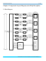
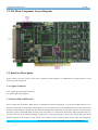
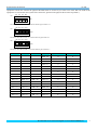
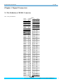
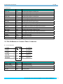
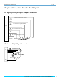
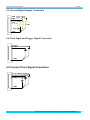
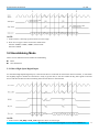
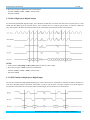
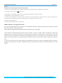
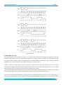
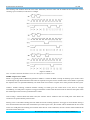
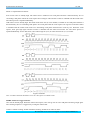
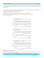
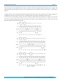
PCI2510 User’s Manual Beijing ART Technology Development Co., Ltd. PCI2510 Data Acquisition V6.108 Contents Contents ................................................................................................................................................................................2 Chapter 1 Overview ..............................................................................................................................................................3 Chapter 2 Components Layout Diagram and a Brief Description .......................................................................................6 2.1 Block Diagram ........................................................................................................................................................6 2.2 The Main Component Layout Diagram ..................................................................................................................7 2.3 Interface Description...............................................................................................................................................7 2.3.1 Signal Connector..........................................................................................................................................7 2.3.2 Physical ID of DIP Switch ...........................................................................................................................7 Chapter 3 Signal Connectors................................................................................................................................................9 3.1 The Definition of DI/DO Connector .......................................................................................................................9 3.2 The Definition of Counter/Timer Connector.........................................................................................................10 Chapter 4 Connection Ways for Each Signal......................................................................................................................11 4.1 High-speed Digital Input /Output Connection ......................................................................................................11 4.2 General Digital Input Connection .........................................................................................................................11 4.3 General Digital Output Connection ......................................................................................................................12 4.4 Clock Input and Trigger Signal Connection..........................................................................................................12 4.5 Counter/Timer Signal Connection ........................................................................................................................12 Chapter 5 Transfer Mode ....................................................................................................................................................13 5.1 Normal Mode ........................................................................................................................................................13 5.1.1 High-speed Digital Input............................................................................................................................13 5.1.2 High-speed Digital Output .........................................................................................................................13 5.2 Handshaking Mode ...............................................................................................................................................14 5.2.1 Burst High-Speed Digital Input .................................................................................................................14 5.2.2 Burst High-Speed Digital Output...............................................................................................................15 5.2.3 8255 Emulation High-Speed Digital Input.................................................................................................15 5.2.4 8255 Emulation High-Speed Digital Output..............................................................................................16 Chapter 6 Methods of Using Timer/Counter.......................................................................................................................16 6.1 The Working Mode ...............................................................................................................................................16 Chapter 7 Notes and Warranty Policy ................................................................................................................................24 7.1 Notes .....................................................................................................................................................................24 7.2 Warranty Policy.....................................................................................................................................................24 Products Rapid Installation and Self-check ........................................................................................................................25 Rapid Installation ........................................................................................................................................................25 Self-check ...................................................................................................................................................................25 Delete Wrong Installation ...........................................................................................................................................25 BUY ONLINE at art-control.com/englishs or CALL+86-10-51289836(CN) 2 PCI2510 Data Acquisition V6.108 Chapter 1 Overview The PCI2510 is a 32-ch Digital I/O card for PCI bus. Its digital I/O channels are TTL-compatible. Unpacking Checklist Check the shipping carton for any damage. If the shipping carton and contents are damaged, notify the local dealer or sales for a replacement. Retain the shipping carton and packing material for inspection by the dealer. Check for the following items in the package. If there are any missing items, contact your local dealer or sales. ¾ PCI2510 Data Acquisition Board ¾ ART Disk a) user’s manual (pdf) b) drive c) catalog ¾ Warranty Card FEATURES Specifications Features ¾ ¾ ¾ ¾ ¾ ¾ ¾ ¾ ¾ ¾ ¾ ¾ ¾ ¾ ¾ ¾ High-speed Channel: 32 (TTL compatible) Port: port PA, port PB, port PC, port PD (8-bit/port) Input and Output Port Settings: 32DI (PA ~ PD) (default), 32DO (PA ~ PD), 16DI (PA ~ PB) & 16DO (PC ~ PD), 8DI (PA) & 8DO (PC) (programmable) On-board FIFO: DI:16KB, DO:16KB Terminator: on-board Schottky diode termination Messaging: the message can be generated when: 1) specified number of bytes has been transferred; 2) when a specified input pattern is matched; 3) when a measurement operation completes. Input Level: High-level: ≥2V Low-level: ≤0.8V Input Load: terminator resistor is 110Ω, the terminator voltage is 2.9V: low-level +0.5V@±22.4mA, high-level +2.7V@±1mA (max). terminator OFF (TTL compatible), low-level +0.5V@±20mA, high-level +2.7V@±1mA (max). Output Level: High-level: ≥2.7V Low-level: ≤0.5V Driving Capacity: low-level: 0.5V max @ +48mA (sink), high-level: +2.4V min @ -15mA (Source) Hysteresis: 500mV Power Interface: +4.65 ~ +5.25 VDC @ 1A General DIO (TTL compatible): 4 channel digital inputs, 4channel digital outputs Interrupt Source: DI0~7 and Timer#2, Pattern match and Change detection, DI FIFO overflow and DO FIFO underflow, DI_STP and DO_STP Power Consumption: Typical: Termination resistor ON: [email protected], termination resistor OFF: [email protected] Maximum: Termination resistor ON: [email protected], termination resistor OFF: [email protected] Operating Temperature: 0℃~ +50℃ BUY ONLINE at art-control.com/englishs or CALL+86-10-51289836(CN) 3 PCI2510 Data Acquisition ¾ ¾ V6.108 Storage Temperature: - 20℃~ +70℃ Relative Humidity: 5 ~ 95% Transfer Characteristics ¾ ¾ ¾ ¾ Data Transfer Mode: Bus Mastering DMA Data Transfer Bus Width: 8/16/32 bits (programmable) Max. Transfer Rate: DI: 40MB/sec, 32-bit@10MHz 120MB/sec, 32-bit@40MHz external trigger (when data length is less than FIFO size) DO: 40MB/sec, 32-bit@10MHz Operation Mode: Handshaking Handshaking Mode ¾ ¾ ¾ ¾ ¾ Direction: I/O Samples No.: Finite transfer, Continuous I/O Asynchronous: 8255 Emulation Synchronous: burst Handshaking Clock source for Burst Handshaking: Internal: 20MHz, 15MHz, 10MHz, internal clock External: CLKIN Normal Mode ¾ ¾ ¾ ¾ ¾ ¾ Input: Data Acquisition at a predetermined rate by internal/external clock Output: output waveform at a predetermined rate by internal/external clock Clock Source for DI: Internal: 20MHz, 15MHz, 10MHz, internal clock External: CLKIN Clock Source for DO: Internal: 20MHz, 15MHz, 10MHz, internal clock External: CLKIN Start Mode Software command / Trigger signal occurred from DI_STR or DO_STR / Pattern DI Stop Mode Software command / Trigger signal occurred from DI_STP or DO_STR / Pattern DI / "Finite transfers" Change Detection ¾ ¾ ¾ ¾ DI Only: monitor the selected input channel and capture data whenever there is a transition on one of the channels, and then issue a IRQ Clock Source for DI: Internal: 20MHz, 15MHz, 10MHz, internal clock External: CLKIN Start Mode: Software command / Trigger signal occurred from DI_STR /Pattern DI Stop Mode: Software command / Trigger signal occurred from DI_STP /Pattern DI / "Finite transfers" Trigger Function ¾ ¾ ¾ ¾ ¾ ¾ ¾ DI Trigger Signal: DI_STR, DI_STP DO Trigger Signal: DO_STR, DO_STP Low-level: 0.8 V max. High-level: 2.0 V min. Trigger Type: rising or falling edge, or digital pattern (for DI only) Pulse Width for Edge Triggers: 10 ns min. Pattern Trigger Detection Capabilities: Detect pattern match on user-selected data lines BUY ONLINE at art-control.com/englishs or CALL+86-10-51289836(CN) 4 PCI2510 Data Acquisition V6.108 Trigger ¾ ¾ ¾ ¾ Trigger Channel: 3, Timer 0 to 2 Resolution: 16-bit Trigger Time Base: 10MHz Timer 2: interrupt source General DIO ¾ ¾ ¾ ¾ Channel NO.: 4 channel digital inputs, 4channel digital outputs Electrical Standard: TTL compatible DI: high-level: 2V min low-level: 0.8V max DO: high-level: 2.4V min low-level: 0.5V max Other Features ¾ ¾ On-board Clock Oscillator: 50MHz Board Dimension: 161mm (L)*101mm (W) BUY ONLINE at art-control.com/englishs or CALL+86-10-51289836(CN) 5 PCI2510 Data Acquisition V6.108 Chapter 2 Components Layout Diagram and a Brief Description 2.1 Block Diagram REG D16~D23 REG Active Terminator Port A 8 I/O 16K FIFO REG SCSI II 100pin Connector REG D0~D7 REG D24~D31 REG Active Terminator Port B 8 I/O 16K FIFO REG REG D8~D15 REG D0~D7 PCI BUS PLX PCI 9054 REG Active Terminator Port C 8 I/O 16K FIFO REG REG D16~D23 REG D8~D15 REG Port D 8 I/O 16K FIFO REG Active Terminator REG D24~D31 Address Bus Control Bus Data Bus Control/ Timing/ Interrupt Logic DI_ACK DI_REQ CLKIN DI_STR DI_STP DI0-3 DO_ACK DO_REQ CLKOUT DO_STR DO_STP DO0-3 BUY ONLINE at art-control.com/englishs or CALL+86-10-51289836(CN) 6 PCI2510 Data Acquisition V6.108 2.2 The Main Component Layout Diagram 2.3 Interface Description Please refer to the first section of the main component layout diagram, to understand the general function of the following main components. 2.3.1 Signal Connector CN1: digital input and output connector P1: Timer input and output port 2.3.2 Physical ID of DIP Switch SW1: Set physical ID number. When the PC is installed more than one PCI2510 , you can use the DIP switch to set a physical ID number for each board, which makes it very convenient for users to distinguish and visit each board in the progress of the hardware configuration and software programming. The following four-place numbers are expressed by the binary system: When DIP switch points to "ON", that means "1", and when it points to the other side, that means "0." As they are shown in the following diagrams: place "ID3" is the high bit."ID0" is the low bit, and the black part in the diagram represents the location of the switch. (Test software of the company often use the logic ID management BUY ONLINE at art-control.com/englishs or CALL+86-10-51289836(CN) 7 PCI2510 Data Acquisition V6.108 equipments and at this moment the physical ID DIP switch is invalid. If you want to use more than one kind of the equipments in one and the same system at the same time, please use the physical ID as much as possible.). ON ID3 ID2 ID1 ID0 ON DID1 1 2 3 4 The above chart shows"1111", so it means that the physical ID is 15. ON ID3 ID2 ID1 ID0 ON DID1 1 2 3 4 The above chart shows"0111", so it means that the physical ID is 7. ON ID3 ID2 ID1 ID0 ON DID1 1 2 3 4 The above chart shows"0101", so it means that the physical ID is 5. ID3 OFF(0) ID2 OFF(0) ID1 OFF(0) ID0 OFF(0) 0 0 OFF(0) OFF(0) OFF(0) ON(1) 1 1 OFF(0) OFF(0) ON(1) OFF(0) 2 2 OFF(0) OFF(0) ON(1) 3 3 OFF(0) OFF(0) 4 4 OFF(0) ON(1) ON(1) ON(1) OFF(0) 5 ON(1) ON(1) OFF(0) 5 OFF(0) OFF(0) ON(1) 6 6 OFF(0) ON(1) ON(1) 7 7 ON(1) OFF(0) OFF(0) ON(1) OFF(0) 8 8 ON(1) OFF(0) OFF(0) 9 9 ON(1) OFF(0) ON(1) A 10 ON(1) OFF(0) ON(1) B 11 ON(1) ON(1) OFF(0) C 12 ON(1) ON(1) OFF(0) D 13 ON(1) ON(1) ON(1) ON(1) OFF(0) E 14 ON(1) ON(1) ON(1) ON(1) F 15 ON(1) OFF(0) ON(1) OFF(0) Physical ID(Hex) Physical ID(Dec) BUY ONLINE at art-control.com/englishs or CALL+86-10-51289836(CN) 8 PCI2510 Data Acquisition V6.108 Chapter 3 Signal Connectors 3.1 The Definition of DI/DO Connector CN1: 100- pin definition DGND DGND DGND DGND DGND DGND DGND DGND DGND DGND DGND DGND DGND DGND DGND DGND DGND DGND DGND DGND DGND DGND DGND DGND DGND DGND DGND DGND DGND DGND DGND DGND DGND DGND DGND DGND DGND DGND DGND DGND DGND DGND DGND DGND DGND DGND DGND DGND DGND DGND 100 50 99 49 98 48 97 47 96 46 95 45 94 44 93 43 92 42 91 41 90 40 89 39 88 38 87 37 86 36 85 35 84 34 83 33 82 32 81 31 80 30 79 29 78 28 77 27 76 26 75 25 74 24 73 23 72 22 71 21 70 20 69 19 68 18 67 17 66 16 65 15 64 14 63 13 62 12 61 11 60 10 59 9 58 8 57 7 56 6 55 5 54 4 53 3 52 2 51 1 CLKOUT CLKIN DO_STP DO_STR DI_STP DI_STR DO_ACK DO_REQ DI_ACK DI_REQ DO3 DO2 DO1 DO0 DI3 DI2 DI1 DI0 PD7 PD6 PD5 PD4 PD3 PD2 PD1 PD0 PC7 PC6 PC5 PC4 PC3 PC2 PC1 PC0 PB7 PB6 PB5 PB4 PB3 PB2 PB1 PB0 PA7 PA6 PA5 PA4 PA3 PA2 PA1 PA0 BUY ONLINE at art-control.com/englishs or CALL+86-10-51289836(CN) 9 PCI2510 Data Acquisition V6.108 Pin definition Signal Name Type Definition PA0~PA7 Input Digital inputs/outputs of the PA port. PB0~PB7 Input Digital inputs/outputs of the PB port. PC0~PC7 Input Digital inputs/outputs of the PC port. PD0~PD7 Input Digital inputs/outputs of the PD port. DI0~DI3 Input 4 channels general digital input. DO0~DO3 Output 4 channels general digital output. DI_REQ Input Digital input channel request signal. DI_ACK Output Digital input channel response signal. DI_STR Input The trigger start signal of the digital input channels. DI_STP Input The trigger stop signal of the digital input channels. DO_REQ Output Digital output channel request signal. DO_ACK Input Digital output channel response signal. DO_STR Input The trigger start signal of the output input channels. DO_STP Input The trigger stop signal of the output input channels. CLKIN Input External clock input. CLKOUT Output Internal clock output. DGND GND Digital ground. 3.2 The Definition of Counter/Timer Connector P1: 10- pin definition CLK0 1 2 GATE0 CLK1 3 4 GATE1 CLK2 5 6 GATE2 OUT0 7 OUT1 DGND 9 8 10 OUT2 Signal Name Type Definition CLK0~CLK2 Input Clock/plus input pin. GATE0~GATE2 Input Gate control input pin. OUT0~OUT2 Output Counter/Timer output pin. DGND GND Digital ground. BUY ONLINE at art-control.com/englishs or CALL+86-10-51289836(CN) 10 PCI2510 Data Acquisition V6.108 Chapter 4 Connection Ways for Each Signal 4.1 High-speed Digital Input /Output Connection PA0 The input/output signal of the PA PA7 PB0 The input/output signal of the PB PB7 Digital Port PC0 The input/output signal of the PC PC7 PD0 The input/output signal of the PD PD7 DGND 4.2 General Digital Input Connection BUY ONLINE at art-control.com/englishs or CALL+86-10-51289836(CN) 11 PCI2510 Data Acquisition V6.108 4.3 General Digital Output Connection 4.4 Clock Input and Trigger Signal Connection 4.5 Counter/Timer Signal Connection BUY ONLINE at art-control.com/englishs or CALL+86-10-51289836(CN) 12 PCI2510 Data Acquisition V6.108 Chapter 5 Transfer Mode PCI2510 provides two types of transmit modes for sample input data from external device to the PCI2510 or output data from PCI2510 to external device. Normal Mode Handshaking Mode 5.1 Normal Mode 5.1.1 High-speed Digital Input In Normal mode of PCI2510, you can start to transmit the data from external device to the PCI2510 by start signal or stop it by stop signal. You can generate start or stop signal by software command, external trigger via DI_STR/DI_STP and pattern DI. When PCI2510 gets the start signal, it will start to receive data from external device at next clock (Point A). When PCI2510 gets the stop signal, it will stop to receive the data at next clock (Point B). NOTE: 1. In this instance, start/stop signal are shown as active high. 2. Note that you can’t generate start and stop signal by pattern DI at the same time. 3. There are two types of DI clock source listed below. Internal: 20MHz, 15MHz, 10MHz, internal clock External: CLKIN 5.1.2 High-speed Digital Output In Normal mode of PCI2510, you can start to transmit the data from PCI2510 to the external device by start signal or stop it by stop signal. You can generate start or stop signal by software command, external trigger via DO_STR/DO_STP. When PCI2510 gets the start signal, it will start to send data to external device at next clock (Point A). When PCI2510 gets the stop signal from external device, it will stop to send the data at next clock (Point B). BUY ONLINE at art-control.com/englishs or CALL+86-10-51289836(CN) 13 PCI2510 Data Acquisition V6.108 NOTE: 1. In this instance, start/stop signal are shown as active high. 2. There are two types of DO clock source listed below. Internal: 20MHz, 15MHz, 10MHz, internal clock External: CLKIN 5.2 Handshaking Mode There are two different transmit modes for handshaking. Burst 8255 Emulation. 5.2.1 Burst High-Speed Digital Input For the Burst High-Speed Digital Input, if the external device would like to transmit the data to PCI2510, it will enable the DI_REQ signal to PCI2510. If PCI2510 is ready to get the data, it will also enable the DI_ACK signal to external device and then the data will be transmitting from external device to the PCI2510. NOTE: 1. In this instance, DI_REQ and DI_ACK signal are shown as active high. BUY ONLINE at art-control.com/englishs or CALL+86-10-51289836(CN) 14 PCI2510 Data Acquisition V6.108 2. There are two types of DI clock source listed below. Internal: 20MHz, 15MHz, 10MHz, internal clock External: CLKIN 5.2.2 Burst High-Speed Digital Output For the Burst High-Speed Digital Output, if the PCI2510 would like to transmit the data to the external device, it will enable the DO_REQ signal to external device. If the external device is ready to get the data, it will also enable the DO_ACK signal to PCI2510 and then the data will be transmitting from PCI2510 to the external device. NOTE: 1. In this instance, DO_REQ and DO_ACK signal are shown as active high. 2. There are two types of DO clock source listed below. Internal: 20MHz, 15MHz, 10MHz, internal clock External: CLKIN 5.2.3 8255 Emulation High-Speed Digital Input For the 8255 Emulation High-Speed Digital Input, if the external device would like to transmit the data to PCI2510, it will send a DI_REQ signal to PCI2510. If PCI2510 is ready to get the data, it will also response a DI_ACK signal to external device and then one unit of data will be transmitting from external device to the PCI2510. BUY ONLINE at art-control.com/englishs or CALL+86-10-51289836(CN) 15 PCI2510 Data Acquisition V6.108 The DI_REQ and DI_ACK signal are shown as active low ONLY in handshaking mode of 8255 Emulation. 5.2.4 8255 Emulation High-Speed Digital Output For the 8255 Emulation Ultra-Speed Digital Output, the PCI2510 would like to transmit the data to the external device; it will send a DO_REQ signal to external device. If the external device is ready to get the data, it will also response a DO_ACK signal to PCI2510 and then one unit of data will be transmitting from PCI2510 to the external device. NOTE: The DO_REQ and DO_ACK signal are shown as active low ONLY in handshaking mode of 8255 Emulation. Chapter 6 Methods of Using Timer/Counter 6.1 The Working Mode MODE 0 Interrupt on terminal count Mode 0 is typically used for event counting. After the Control Word is written, OUT is initially low, and will remain low until the Counter reaches zero. OUT then goes high and remains high until a new count or a new Mode 0 Control Word is written into the Counter. BUY ONLINE at art-control.com/englishs or CALL+86-10-51289836(CN) 16 PCI2510 Data Acquisition V6.108 GATE=1 enables counting; GATE=0 disables counting. GATE has no effect on OUT. After the Control Word and initial count are written to a Counter, the initial count will be loaded on the next CLK pulse. This CLK pulse does not decrement the count, so for an initial count of N, OUT does not go high until N+1 CLK pulses after the initial count is written. If a new count is written to the Counter, it will be loaded on the next CLK pulse and counting will continue from the new count. If a two-byte count is written, the following happens: 1) Writing the first byte disables counting. OUT is set low immediately (no clock pulse required) 2) Writing the second byte allows the new count to be loaded on the next CLK pulse This allows the counting sequence to be synchronized by software. Again, OUT does not go high until N+1 CLK pulses after the new count of N is written. If an initial count is written while GATE=0, it will still be loaded on the next CLK pulse. When GATE goes high, OUT will go high N CLK pulse later, no CLK pulse is needed to load the Counter as this has already been done. Figure 6.1 Mode 0 BUY ONLINE at art-control.com/englishs or CALL+86-10-51289836(CN) 17 PCI2510 Data Acquisition V6.108 NOTE The following conventions apply to all mode timing diagrams 1. Counters are programmed for binary (not BCD) counting and for reading/writing least significant byte (LSB) only. 2. The counter is always selected ( CS always low) 3. CW stands for “Control Word”; CW=10 means a control word of 10 HEX is written to the counter. 4. LSB stands for “Least Significant Byte” of count. 5. Numbers below diagrams are count values. The lower number is the least significant byte. The upper number is the most significant byte. Since the counter is programmed to read/writer LSB only, the most significant byte cannot be read. N stands for an undefined count. Vertical lines show transitions between count values. MODE 1 Hardware retriggerable one-shot OUT will be initially high. OUT will go low on the CLK pulse following a trigger to begin the one-shot pulse, and will remain low until the Counter reaches zero. OUT will then go high and remain high until the CLK pulse after the next trigger. After writing the Control Word and initial count, the Counter is armed. A trigger results in loading the Counter and setting OUT low on the next CLK pulse, thus starting the one-shot pulse. An initial count of N will result in a one-shot pulse N CLK cycles in duration. The one-shout is retriggerable, hence OUT will remain low for N CLK pulses after any trigger. The one-shot pulse can be repeated without rewriting the same count into the counter. GATE has no effect on OUT. If a new count is written to the Counter during a one-shot pulse, the current one-shot is not affected unless the counter is retriggered. In that case, the Counter is loaded with the new count and the one-shot pulse continues until the new count expires. BUY ONLINE at art-control.com/englishs or CALL+86-10-51289836(CN) 18 PCI2510 Data Acquisition V6.108 Figure6.2 Mode 1 MODE 2 Rate Generator This Mode functions like a divide-by-N counter. It is typically used to generate a Real Time Clock interrupt. OUT will initially be high. When the initial count has decremented to 1, OUT goes low for on CLK pulse. OUT then goes high again, the Counter reloads the initial count and the process is repeated. Mode 2 is periodic; the same sequence is repeated indefinitely. For an initial count of N, the sequence repeats every N CLK cycles. GATE=1 enables counting; GATE=0 disables counting. If GATE goes low during an output pulse, OUT is set high immediately. A trigger reloads the Counter with the initial count on the next CLK pulse; OUT goes low N CLK pulses after the trigger. Thus the GATE input can be used to synchronize the Counter. After writing a Control Word and initial count, the Counter will be loaded on the next CLK pulse. OUT goes low N CLK Pulses after the initial count is written. This allows the Counter to be synchronized by software also. Writing a new count while counting does not affect the current counting sequence. If a trigger is received after writing a new count but before the end of the current period, the Counter will be loaded with the new count on the next CLK pulse BUY ONLINE at art-control.com/englishs or CALL+86-10-51289836(CN) 19 PCI2510 Data Acquisition V6.108 and counting will continue from the new count. Otherwise, the new count will be loaded at the end of the current counting cycle. In mode2, a COUNT of 1 I illegal. Figure 6.3 Mode 2 Note: A GATE transition should not occur one clock prior to terminal count. MODE 3 Square wave mode Mode 3 is typically used for Baud rate generation. Mode 3 is similar to Mode 2 except for the duty cycle of OUT. OUT will initially be high. When half the initial count has expired, OUT goes low for mainder of the count. Mode 3 is periodic; the sequence above is repeated indefinitely. An initial count of N results in a square wave with a period of N CLK cycles. GATE=1 enables counting; GATE=0 disables counting. If GATE goes low while OUT is low, OUT is set high immediately; no CLK pulse is required. A trigger reloads the Counter with the initial count on the next CLK pulse. Thus the GATE input can be used to synchronize the Counter After writing a Control Word and initial count, the Counter will be loaded on the next CLK pulse. This allows the Counter to be synchronized by software also. Writing a new count while counting does not affect the current counting sequence. If a trigger is received after writing a new count but before the end of the current half-cycle of the square wave, the Counter will be loaded with the new count on the next CLK pulse and counting will continue from the new count. Otherwise, the new counter will be loaded at the end of the current half-cycle. BUY ONLINE at art-control.com/englishs or CALL+86-10-51289836(CN) 20 PCI2510 Data Acquisition V6.108 Mode 3 is implemented as follows: Even counts: OUT is initially high. The initial count is loaded on one CLK pulse and then is decremented by two on succeeding CLK pulses. When the count expires OUT changes value and the Counter is reloaded with the initial count. The above process is repeated indefinitely. Odd counts: OUT is initially high. The initial count minus one (an even number) is loaded on one CLK pulse and then is decremented by two on succeeding CLK pulses. One CLK pulse after the count expires. OUT goes low and the Counter is reloaded with the initial count minus one. Succeeding CLK pulses decrement the count by two. When the count expires, OUT goes high again and the Counter is reloaded with the initial count minus one. The above process is repeated indefinitely. So for odd counts, OUT will be high for (N+1)/2 counts and low for (N-1)/2 counts. Figure 6.4 Mode 3 Note: A GATE transition should not occur one clock prior to terminal count. MODE 4 Software triggered strobe OUT will be initially high. When the initial count expires, OUT will go low for one CLK pulse and then go high again. The counting sequence is “triggered” by writing the initial count. GATE=1 enables counting; GATE=0 disables counting. GATE has no effect on OUT. BUY ONLINE at art-control.com/englishs or CALL+86-10-51289836(CN) 21 PCI2510 Data Acquisition V6.108 After writing a Control Word and initial count, the Counter will be loaded on the next CLK pulse. This CLK pulse does not decrement the count, so for an initial count of N, OUT does not strobe low until N+1 CLK pulses after the initial count is written. If a new count is written during counting, if will be loaded on the next CLK pulse and counting will continue from the new count. If a two-byte count is written, the following happens: 1) Writing the first byte has no effect on counting. 2) Writing the second byte allows the new count to be loaded on the next CLK pulse. This allows the sequence to be ‘‘retriggered’ by software. OUT strobe low N+1 CLK pulses after the new count of N is written. Figure 6.5 Mode 4 MODE 5 Hardware triggered strobe OUT will initially be high. Counting is triggered by a rising edge of GATE. When the initial count has expired, OUT will go low for one CLK pulse and then go high again. BUY ONLINE at art-control.com/englishs or CALL+86-10-51289836(CN) 22 PCI2510 Data Acquisition V6.108 After writing the Control Word and initial count, the counter will not be loaded until the CLK pulse after a trigger. This CLK pulse does not decrement the count, so for an initial count of N, OUT does not strobe low until N+ 1 pulse after a trigger. A trigger results in the Counter being loaded with the initial count on the next CLK pulse. The counting sequence is retriggerable. OUT will not strobe low for N+1 CLK pulses after any trigger. GATE has no effect on OUT. If a new count is written during counting, the current counting sequence will not be affected. If a trigger occurs after the new count is written but before the current count expires, the Counter will be loaded with the new count on the next CLK pulse and counting will continue from there. Figure 6.6 Mode 5 BUY ONLINE at art-control.com/englishs or CALL+86-10-51289836(CN) 23 PCI2510 Data Acquisition V6.108 Chapter 7 Notes and Warranty Policy 7.1 Notes In our products’ packing, user can find a user manual, a PCI2510 module and a quality guarantee card. Users must keep quality guarantee card carefully, if the products have some problems and need repairing, please send products together with quality guarantee card to ART, we will provide good after-sale service and solve the problem as quickly as we can. When using PCI2510, in order to prevent the IC (chip) from electrostatic harm, please do not touch IC (chip) in the front panel of PCI2510 module. 7.2 Warranty Policy Thank you for choosing ART. To understand your rights and enjoy all the after-sales services we offer, please read the following carefully. 1. Before using ART’s products please read the user manual and follow the instructions exactly. When sending in damaged products for repair, please attach an RMA application form which can be downloaded from: www.art-control.com. 2. All ART products come with a limited two-year warranty: ¾ The warranty period starts on the day the product is shipped from ART’s factory ¾ For products containing storage devices (hard drives, flash cards, etc.), please back up your data before sending them for repair. ART is not responsible for any loss of data. ¾ Please ensure the use of properly licensed software with our systems. ART does not condone the use of pirated software and will not service systems using such software. ART will not be held legally responsible for products shipped with unlicensed software installed by the user. 3. Our repair service is not covered by ART's guarantee in the following situations: ¾ Damage caused by not following instructions in the User's Manual. ¾ Damage caused by carelessness on the user's part during product transportation. ¾ Damage caused by unsuitable storage environments (i.e. high temperatures, high humidity, or volatile chemicals). ¾ Damage from improper repair by unauthorized ART technicians. ¾ Products with altered and/or damaged serial numbers are not entitled to our service. 4. Customers are responsible for shipping costs to transport damaged products to our company or sales office. BUY ONLINE at art-control.com/englishs or CALL+86-10-51289836(CN) 24 PCI2510 Data Acquisition V6.108 5. To ensure the speed and quality of product repair, please download an RMA application form from our company website. Products Rapid Installation and Self-check Rapid Installation Product-driven procedure is the operating system adaptive installation mode. After inserting the disc, you can select the appropriate board type on the pop-up interface, click the button【driver installation】; or select CD-ROM drive in Resource Explorer, locate the product catalog and enter into the APP folder, and implement Setup.exe file. After the installation, pop-up CD-ROM, shut off your computer, insert the PCI card. If it is a USB product, it can be directly inserted into the device. When the system prompts that it finds a new hardware, you do not specify a drive path, the operating system can automatically look up it from the system directory, and then you can complete the installation. Self-check At this moment, there should be installation information of the installed device in the Device Manager (when the device does not work, you can check this item.). Open "Start -> Programs -> ART Demonstration Monitoring and Control System -> Corresponding Board -> Advanced Testing Presentation System", the program is a standard testing procedure. Based on the specification of Pin definition, connect the signal acquisition data and test whether AD is normal or not. Connect the input pins to the corresponding output pins and use the testing procedure to test whether the switch is normal or not. Delete Wrong Installation When you select the wrong drive, or viruses lead to driver error, you can carry out the following operations: In Resource Explorer, open CD-ROM drive, run Others-> SUPPORT-> PCI.bat procedures, and delete the hardware information that relevant to our boards, and then carry out the process of section I all over again, we can complete the new installation. BUY ONLINE at art-control.com/englishs or CALL+86-10-51289836(CN) 25