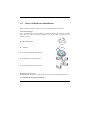
1
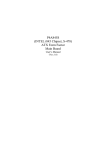
P4M845
(INTEL i845 Chipset, S-478)
Mirco-ATX Form Factor
Main Board
User’s Manual
(Ver.:1.0)
Copyright
Copyright©2001 by this company. No part of this document may be
reproduced, transmitted, transcribed, stored in a retrievable system,
or translated into any natural or computer language, in any form or
by any means without prior written permission. This manual and the
information contained here are protected by copyright. All rights
reserved.
Copyright 2001. All Rights Reserved.
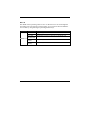
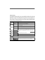
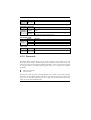
Revision History
Revision
1.0
Date
Oct. -2001
Release Notes
First Official Release
Warning and disclaimer
This manual is designed to provide information about the Pentium®4
main board. Every has effort have been made to make this manual as
accurate as possible, but no warranty or fitness is implied. All the
information is provided on an 'as is' basis. The author and his
corresponding publishing company shall have neither liability nor
responsibility to any person or entity with respect to any loss or
damages arising from the information contained in this manual or
from the use of the system board that accompanies it.
Information contained in this manual is subject to change without
notice. The manufacturer of the system board will not be held
responsible for technical or editorial omissions made herein, nor for
the incidental or consequential damages resulting from its
furnishing, performance, functionality or use. Subsequent changes to
this manual will be incorporated into the next edition. We welcome
any suggestion regarding this manual or our computer products.
Trademarks
● Intel® and Pentium® are registered trademarks of Intel® Corporation.
● IBM® is a registered trademark of International Business Machines
Corporation.
● Microsoft® is a registered trademark of Microsoft® Corporation.
● PCI® is a registered trademark of PCI® Special Interest Groups.
● AWARD® is a registered trademark of Award Software Inc.
All other trademarks are the property of their respective owners.
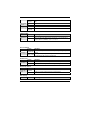
Table of Contents
Chapter 1
1-1
1-2
1-3
Main Specifications……………………………………………………4
System Configuration……………………………………………..……6
Notice of Hardware Installation………….……………………....……7
Chapter 2
2-1
2-2
2-3
2-3-1
2-3-2
2-4
2-4-1
2-5
2-5-1
2-5-2
2-5-3
2-5-4
2-5-5
2-5-6
2-5-7
2-5-8
2-6
2-6-1
Installation……………….……………………….…8
Component Locations …………………..…………………………..…8
Layout Reference……………………………………………..………..9
Jumper Setting……………………………………..………..……….10
JP2/ JP7: USB Wake Up Function…………………………………10
JP3: Keyboard Wake Up Function…………………………………11
CPU Installation………………. ……………………………………12
CPU and System Cooling………………………….…………………15
Connectors………..……………………………………………………16
Front Panel…………………………………………………….………17
Back Panel Connectors………………………………………………18
Power Supply Connector……………………………………………20
Floppy Disk Connector………………………………………………21
IDE1 and IDE2………………………………………………………22
IR1: IrDA (InfraRed Remote Link) Connector……………………23
Internal Audio Connecotrs……………………………………………24
WOL1:WakeUp On LAN (Optional)………………………………25
Memory………………………………………………………………26
Memory Installation…………………………………………………27
Chapter 3
3-1
3-2
Introduction…………………………………………3
Software Installation………………………………28
Notice of Driver Installation…………………………………………28
How to Install Software Drivers…………………………………….29
1
Chapter 4
4-1
4-2
4-3
4-3-1
4-3-2
4-3-3
4-3-4
4-3-5
4-3-6
4-3-7
4-3-8
4-3-9
Updating the BIOS……………………………………………………31
The CMOS Memory…………………………………………………32
The BIOS Setup Pages………………………………………………34
Standard CMOS Setup………………………………………………37
BIOS Features Setup…………………………………………………41
Chipset Features Setup………………………………………..……45
Integrated Peripherals………………………………………..……...48
Power Management Setup………………………………………….53
PNP/PCI Configuration Setup……………………………………….56
PC Health Status……………………………………………………58
Frequency/Voltage Control.…………………………………………59
Passwords Setting…………………………………………………….60
Chapter 5
5-1
5-2
5-3
5-4
5-5
5-6
The BIOS…..………………………………………30
Appendix…………………………………………62
Memory Map………………………………………………….………62
I/O Map………………………………...….………………………….63
Time & DMA Channels Map…………………………………………64
Interrupt Map………………………………………….……………...65
RTC & CMOS RAM Map………………………………………….66
ISA I/O Address Map……………………………………………67
Chapter 6
Q & A………………………………………………… ………… ……69
Important Warnings:
STOP
WARNING: NEVER run the processor without the heatsink properly and firmly
attached. This will damage the processor within SECONDS. Also do NOT try to use
Pentium Heatsinks, these will NOT fit and do NOT provide adequate cooling.
STOP
WARNING: Make sure your power supply can deliver the power your system needs.
We recommend AT LEAST a 250W power supply. Even better, get a 300W power
supply, especially when using many peripherals.
2
Chapter 1
Introduction
Thank you for purchasing this high quality motherboard, we are confident that you will be
able to use this motherboard to your full satisfaction. This manual is divided into 6 main
sections, as described below:
.
Introduction
The introduction contains information on the main specifications for this motherboard, the
package contents and cautionary notes.
Hardware Installation
The Hardware Installation section is the most important in the manual. It describes in detail
how to set the motherboard up for operation. Read all information and follow all steps,
especially if you are a new user.
Software Installation
The software section describes the drivers that need be installed to make your OS operates
properly. The drivers are provided on the driver CD.
BIOS Setup
Information on how to enter the BIOS setup and change settings is given here. In addition
all individual BIOS items are described. Although some BIOS setting information is given
in the hardware installation section where appropriate, refer to the BIOS Setup Section for
details.
Appendix
Provides useful information
Q&A
3
1-1
Main Specifications
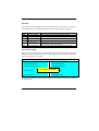
PCB board size and form factor: 22.0cm x 24.5cm, Mirco-ATX form factor.
PCB layer: 4 layers
Supported CPUs
Can support the latest 400MHz system bus Socket-478 Intel P4 CPUs up to 2GHz or higher
speed.
Intel i845 Chipset (Called MCH)
The Intel® i845 chipset consists of the following main components: Intel® Memory
Controller Hub (MCH) and the Intel I/O Controller Hub 2 (ICH2). All these components
are interconneted via and Intel proproetary interface called Hub Interface. The Hub
Interface is designed into the Intel 845 Chipset to provide efficient communication between
components.
Additional hardware platform features include AGP 4x mode, PC 133 System memory,
Ultra ATA/100, and Universal Serial Bus (USB). The platform is also ACPI compliant and
supports Full-on , Suspend to Disk, and Soft-off power management states.
Memory
This motherboard comes equipped with three Dual Inline Memory Module (DIMM)
sockets to support Intel PC100/ PC133 -compliant (8, 16, 32, 64, 128, or 256MB) DIMM
modules up to 768MB.
AGP (Accelerated Graphics Port)
Allows only AGP 2.0, 4X AGP cards. Do not install any graphics cards which
have no support for AGP 4X into i845 and i850 based motherboards.
Otherwise, the AGP slot of your motherboard will be irretrievably damaged
because of the TOO HIGH VOLTAGE (AGP 2X 3.3V, AGP 4X – 1.5V).
STOP
WARNING:ASUS SiS-305 VGA model: AGP-V300C cannot work on this mainboard
even it can fit into AGP slot.
4
PCI Expansion Slots
With three 32-bit PCI (Rev. 2.2) expansion slots, which can support Bus Master PCI cards,
such as LAN or Video-grabber cards (PCI supports up to 133MB/s maximum throughput),
this motherboard is ready for the most demanding applications.
CNR Slot
A Communication Networking Riser (C.N.R.) slot can be fitted with CNR MODEM, or
MODEM/ LAN 10/100M card.
USB interface
With support for up to 4 USB ports, two on-board, this motherboard provides ample USB
expansion room.
IDE interface
This motherboard comes with an onboard PCI Bus Master IDE controller with two
connectors that support four ATA66/ 33 devices on two channels. Supports UDMA/66,
UDMA/33, PIO Modes 3 & 4 and Bus Master IDE DMA Mode 2, and Enhanced IDE
devices, such as CD-R/ RW, DVD-ROM, CD-ROM, Tape Backup and LS-120 drives. An
IDE-3/4 RAID function is optional.
Super Multi-I/O
This functionality is integrated into the southbridge of the chipset. It provides two highspeed UART compatible serial ports and one parallel port with EPP and ECP capabilities.
Infrared (IrDA) Connector
This functionality is also integrated into the southbridge of the chipset. The IrDA connector
supports an optional IR remote control device for wireless interfacing with external
peripherals, personal gadgets, or an optional remote controller.
System BIOS
This motherboard comes with a 2MB BIOS that provides CPU/ SDRAM frequency, boot
block write protection, and HD/ SCSI/ CD/ Floppy boot selection. DMI is also supported
through BIOS, which allows hardware to communicate within a standard protocol creating
a higher level of compatibility.
A.
B.
Special Function
Suspend to memory (S3 mode) is an optional function.
AC-97 Sound Codec chip provides “ amplifier“ function.
5
C.
Allows PIII or P4 power supply but needs minimum 250 Watts when using PIII
Power supply.
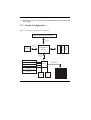
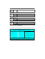
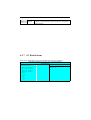
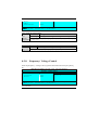
1-2
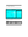
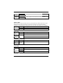
System Configurations
Below is the i845 chipset based system configuration:
Intel Pentium 4 processor
System Bus
3.2GB/s
1.06GB/s
8-Bit Hub
Interface
266MB/s
4 USB 1.1 Ports
2 ATA100 IDE Channels
ICH2
LAN Connect
AC-97 Modem CODEC
(optional)
AC-97 Modem CODEC
(optional)
Flash
BIOS
SIO
6
PCI Bus
PC133
SDRAM
Brookdale
MCH
PC133
SDRAM
AGP 4X (1.5V)
1.06GB/s
PC133
SDRAM
AGP
Graphics
1-3
Notice of Hardware Installation
Before hardware installation, make sure you have checked the following things.
A. Check the package
If any of these items is missing or damaged, contact the dealer from whom you purchase.
Leave this main board in its original package until you are ready to install it. In the
package, there are:
➨ This motherboard
➨ 1 Manual
➨ 1 Driver Installation CD-ROM
➨ 1 IDE ATA 66/100 Flat-Cable
➨ 1 Floppy Disk Drive Flat-Cable
B. Make sure power is off.
During hardware installation, be sure that there is no power connected during this period.
C. Avoid ESD (Electrical Static Discharge.)
7
While installing the main board, wear a grounded wristband or ankle strap to avoid ESD
(Electrical Static Discharge).
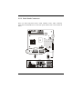
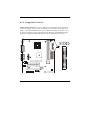
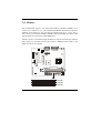
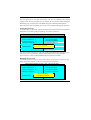
Chapter 2 Installation
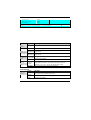
2-1 Component Locations
1
2
3
4
5
6
7
1 ATX Power Supply
2 AUX_1 Power Supply
3 Intel i845 Chipset
4 CPU Socket-478
5 CP_FAN1
6 DIMM
7 AUX_PW1 Power Supply
8 PW_FAN1
9 FDD
10 IDE1 & IDE2
11 FW82801EA
12 WOL1
13 BIOS
14 FAN1
15 BATTERY
16 CNR Slot
17 PCI slot
18 Sound Codec
19 CD_IN1
AUX_IN1
TELE1
20 AGP slot
21 GAME PORT
LINE-IN
LINE-OUT
MIC-IN
22 LPT, COM
23 USB
24 PS/2 Mouse
& K/B
16
15
14
13
8
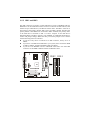
2-2 Layout Reference
PS/2 Mouse
& K/B
AUX_PW1
JP 2
Socket-478
JP 3
PW_FAN1
USB
CP_FAN1
FDD
DIMM3
LPT
DIMM1
DIMM2
COM1
COM2
AGP1
Intel
FW82801BA
IDE2
IDE1
ATX Power
AUX_1
TELE1
AUX_IN1
MIC-IN
GAME
LINE-IN
Intel i845
CD_IN1
LINE-OUT
PCI1
Sound Codec
PCI2
JP 6
SMB1
IR 1
BIOS
PCI3
CNR1
WOL1
JP 7
Battery
FAN1
USB2
RESET
SPEAKER
9
SUSLED SOFT_PWR
HDD_LED PWR_LED
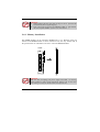
2-3 Jumper Setting
There is no Hardware jumper setting when install CPU, meanwhile user needs
to set correct “CPU clock ration” under “Frequency/ Voltage Control” in the
BIOS, e.g. the ratio for 1.5G CPU is “x15”, 20G CPU is “x20”, …(Please refer
to page 58).
2-3-1 JP2/ JP7: USB Wake Up Function
JP2/ JP7are 3-pin selector which provides USB wake up function. Set “1-2” to
disable and set “2-3” to enable USB wake up function.
JP 2
USB Wake Up
Function Selector
3
2
1
Set "1-2"
Normal (5V USB)
JP 7
3
2
1
Set "2-3"
Enabled USB
Wake Up Function
10
2-3-2 JP3: Keyboard Wake Up Function
JP3 is a 3-pin selector that provides keyboard wake up function. Set ”1-2” to
disabled and set “2-3” to enabled keyboard wake up function.
Keyboard Wake Up
Function Selector
JP 3
3
2
1
Set "1-2"
Normal (default)
3
2
1
Set "2-3"
Enabled Keyboard
Wake Up Function
11
2-4 CPU Installation
The first step in the installation of your CPU is the insertion of the CPU into the 478 pins
CPU socket. Please follow the steps as outlined below carefully to avoid damage to the
CPU.
Avoid Static Electricity
The Intel P4 processors and your motherboard contain sensitive electronic components that
can be easily damaged by static electricity. We recommend that you leave the processor in
its original packaging until you are ready to install it. You should only touch the edges of
the processor, NEVER touch the processor pins to avoid static discharge.
First take a moment to inspect your CPU for obvious damage due to shipping or handling.
Be sure that no noticeable damage exists before proceeding. You should have the following
items:
1 Intel P4 processor.
1 good heatsink and fan assembly.
Step 1
The following figure shows the processor socket. Note that the release lever on the right
side of the socket is down and latched. This position is used to lock the processor in place.
The lever must be raised to install the processor. To do this, first push the lever sideways to
unlatch it, then raise it all the way up (approximately 90 degrees).
Step 2
The processor pin array at the top two corners is angled and has no pins in the corners.
Notice that at the top of the socket on the motherboard (near where it says "Socket 478")
the corners also do not have positions for pins. The processor must be positioned so the
pins match up properly. When you do that, the corner of processor that is cut off will be
positioned next to the release pivot.
It should take no force to install the processor, this is a zero insertion force (ZIF) socket. If
it takes any force you are doing something wrong. Check the pin alignment and also make
sure the release lever is raised up completely.
12
After placing the CPU lower the release lever to lock the processor in place.
Now with the processor properly installed, you can proceed to install the heatsink. It is
important to note that If you have never installed a heatsink on an Intel PIII or Celeron
processor before it may be difficult. We recommend you do a dry run a few times before
doing the final installation. To allow you to do this read the following instructions. Do not
remove the film on the thermally conductive compound until you are ready to do the final
installation.
WARNING: Never run the processor without the heatsink properly
STOP and firmly attached.
Step3
The picture below shows the bottom of the heatsink. Notice the step in the heatsink surface,
this portion fits over the top of the socket, where the legend "Socket 478" is molded into
the plastic. The heatsink must be mounted with this step above the top of the socket or the
heatsink will not be touching the processor properly.
The next picture shows the removal of the plastic film from the thermally conductive
compound. The thermal compound is a thin layer of material that increases the efficiency
of the heatsink by filling microscopic surface voids in the processor or heatsink surface
with a thermally conductive material. Please do not remove the plastic film until you have
practiced installing the heatsink and mounting the clips on the socket. It can take a few tries
to get used to doing this.
13
The following picture shows a side view of the heatsink with the retaining clip at the
bottom of the heatsink. Make sure this retaining clip is at the bottom of the heatsink before
trying to install it.
The following picture shows the non-moveable end of the heatsink retaining clip installed
on the lug at the bottom of the processor socket. This end of the clip simply slides over the
lug when you tilt the heatsink / fan assembly towards the lug.
Now lock the locking clip for the retaining strap over the lug at the other (pivot end) of the
processor socket. This is an easy procedure after you do it a few times, but initially it will
require you to use a finger on one hand to push the latch down and use your other hand to
push the latch in. This is the part you need to practice to install the clip properly. When you
are holding the heatsink, make sure you do apply pressure to the fan. You could damage it
and cause thermal failure of the processor.
WARNING: Be careful not to scrape the motherboard during the mounting
STOP of the fan or else damage may occur to the motherboard.
Now connect the wire from the heatsink fan to the CP_FAN1 connector on the
motherboard. This connector is keyed and can only be installed one way. If you use a
heatsink assembly that has two cooling fans, connect one to CP_FAN and the other
PW_FAN1. For more information on the FAN connectors, refer to the FAN connector
section later in this section.
14
2-4-1 CPU and System Cooling
Any attempt to operate the Intel P4 Processor without a suitable cooling
solution will result in permanent damage to the processor and potentially other
components within the system.
FAN Headers
Your motherboard allows the use of in all 3 FANs. Of these 3 FANs, 1 can be
used by the CPU Heatsink assembly. The other 2 FAN Headers allow
connection of a Chassis Fan and a Power Supply FAN respectively. For a the
location of the FAN connectors, refer to the following picture:
FAN Signal
SY_FAN1
CP_FAN1
PW_FAN1
15
2-5 Connectors
There are many connectors on this main board. Refer to the following pages for
details.
2-5-1 Front Panel
Front panel has connectors as “SPEAKER,” “RESET,” “HDD_LED,”
“SUSLED,” “PWR_LED,” “SOFT_PWR.” Please refer the details as below.
SPEAKER
RESET
HDD_LED
PWR_LED
SYSKED
16
SOFT_LED
17
SPEAKER. is a 4-pin keyed Berg strip. This speaker connector is for the internal
case speaker. This speaker will enable the BIOS to give spoken messages in case
of boot up trouble. The BIOS been codes also use this speaker. For Games and
Music this speaker will not be used, but rather the back panel line-out connector.
RESET connector is a 2 -pin keyed Berg strip, connected to the push button reset
switch on the case front panel. Shorting both pin 1 & pin 2 can reset the system,
which is similar to the power off and then on again.
HDD-LED (Hard Disk activity LED connector) is a 2-pin keyed Berg strip. It is
used to connect to front panel Hard Disk LED. This LED will light up whenever
one of your IDE devices is being accessed.
SUSLED
PWR-LED is a 3-pin connector. It is used to connect to the LED on the case front
panel. The LED shows the status of the power.
SOFT_PWR
18
2-5-2 Back Panel Connectors
There are PS/2 keyboard/ mouse, USB, COM1/2, LPT1, MIC, LINE-IN,
LINE-OUT and GAME Port on case back panel. Please refer to more details as
below.
USB2
PS/2 M ou se
LPT 1
GA ME
USB1
Keyboard
COM 2 LIN E-OU T M IC-IN
LIN E-IN
COM 1
19
COM1/COM2
The onboard serial port 1 and port 2 are the 9-pin D-subminiature male
connector COM1 and COM2. COM1 and COM2 can be disabled in BIOS
setup. Please refer to Chapter 3 “Integrated Peripherals” for more information.
PS2 Keyboard/ Mouse
The Keyboard can be plugged in in only one way. Please do nor force the
connector in, it may get damaged by use of excessive force. It is easy to make
the mistake of reversing the PS/2 keyboard and mouse connectors. If your
keyboard does not work, check this first. The keyboard must be inserted into
the lower connector.
The Mouse can be plugged in in only one way, too. Please do not force the
connector in, it may get damaged by use of excessive force.
LPT
The onboard parallel port is a 25-pin female connector. It supports standard
printer port, Enhanced Parallel Port (EPP), Extended Capabilities Port (ECP),
Standard Parallel Port (SPP).
USB:USB (Universal Serial Bus) Connector
Universal Serial Bus connector, marked as “USB,”is used to connect USB
devices. There are 2 USB connectors on this main board.
Midi/Game Port & External Audio Connectors
Midi/Game port has 15 pins connecting to the game joystick. External Audio
connectors are ”LINE-OUT,LINE-IN, MIC-IN ” for audio functions.
20
2-5-3 Power Supply Connector
This main board needs P4 power supply which contains ATX, AUX_1 &
AUX_PW1 3 power connectors, ATX power supply connector has 20 pins,
which is especially designed for ATX case. AUX_1 power supply connector
has 4 pins. The ATX power supply supports the function of the “Soft Power
On Momentary switch” which connects the front panel switch to the 2-pin
SOFT-PWR on the system board. While the power switch on the back of
ATX power is turned on, the full power will not go into the system board until
the front panel switch is momentarily pressed. Push the switch again to turn off
the power to the system board.
AUX_PW1
AUX_1
ATX POWER
STOP
WARNING:
A. Many P4 power supplies don’t have AUX_PW1 connector. This main board acopts
ATX & AUX_1 2 connectors too.
B. This mainboard also aacepts PIII type poweer but requessts minimm 250W.
Manufactever doesn’t qucivamted for its power function if use PIII power supply.
21
2-5-4 Floppy Disk Connector
Floppy Disk Connector has 34 pins and allows connection of a floppy drive.
In all two floppy drives can be connected to the mother board, known as
floppy A and B. The BIOS allows you to disable the floppy controller if you
do not use any floppy driver, that will free an Interrupt. The BIOS also allows
swapping of floppy A and B although this will not be useful to most users.
FDD
22
2-5-5 IDE1 and IDE2
The IDE connectors are used to connect IDE devices such as Harddisks and CDROM drives to the motherboard. Each connector constitutes an IDE channel, each
channel accepts 2 IDE devices, one Master and one Slave. The IDE 1 connector is
also known as the primary channel, IDE 2 is the secondary channel. Therefore the
primary Master is the IDE device connected to IDE1 as Master, the primary Slave
is the IDE device conneced to IDE 1 as Slave. Jumpers on the IDE device
determine Master and Slave settings. Your harddisk or CD-ROM should have a
sticker with jumper settings. Make sure that you set these jumpers correct. Please
use the following advice as reference:
If you have only device connected to an IDE connector, always set it as
Master.
If you have one HDD and CD-ROM in your system, then connect the HDD
to IDE1 as Master, and the CD-ROM to IDE 2 as Master
If you have one Harddisk and one CD-ROM connected to the same IDE
connector set the HDD to Master and the CD-RAM to Slave.
IDE2 IDE1
23
2-5-6 IR1: IrDA (InfraRed Remote Link) Connetcor
If you want to make use of an Infra Red Remote device you can use IR1, a 5-pin header
on the motherboard. You will need to buy a spearate IR device from your dealer. The
motherboard supports both ASKIR and HPSIR specifications, you will need to set the
standard you want to use in the BIOS on the integrated peripherals page. The pin layout of IR1 is as follows:
IrDA
VCC IRRX GND IRTX
24
2-5-7 Internal Audio Connectors
Internal Audio Connectors are “CD_IN.” It is a CD ROM external audio input signal to
line-out (speaker) of the main board.
CD_IN1 AUX_IN1 TELE1
25
2-5-8 WOL1: Wake up on LAN
Wake up on LAN marked as “WOL1,” is a 3-pin connector. To support this
feature, a network card is required for the system and network management
software must be installed, too.
WOL1
WOL1 (Wake up on LAN) function requirement:
Power supply should be able to offer at least 1A current driving
ability to the signal “5V trickle voltage.”
26
2-6 Memory
This motherboard supports only Dual Inline Memory Modules (DIMMs). Two
sockets are available for 3.3 Volt unbuttered SDRAM (Synchronous Dynamic
Random Access Memory). The sizes that are supported are:8, 16, 32, 64, 128, or
256 , memory sizes between 8MB to 256MB can be formed this way. Refer to the
picture below for the position of the DIMM slots:
Memory speed is controlled through the BIOS, on the Advanced Chipset Features
Setup page you will find several items related to SDRAM speed. Refer to the
BIOS section for more details.
DIMM1
DIMM2
DIMM3
27
STOP
WARNING:
DIMM modules that have more than 18 chips are not supported on this
motherboard. (Due to signal integrity)
If the system CPU bus operates at 100MHz/133MHz, use only PC100/PC133-compliant DIMMs. (System won’t boot otherwise)
2-6-1 Memory Installation
The DIMM modules can be inserted in DIMM slots 1 to 2. Because of the two
notches in the DIMM module it can be inserted in only one way. Please refer to
the picture below for information on how to insert the DIMM modules.
DIMM
STOP
WARNING:
Make sure that you unplug your power supply when adding or removing
memory modules or other system components. Failure to do so may cause
severe damage to both your motherboard and expansion cards
28
Chapter3
3-1
Software Install
Notice of CD Driver Installation
This CD contains below drivers. The user must read “Index” before installing
required drivers. Index offers all the information on all the drivers.
CD driver is always updated with the latest version, so the actual CD
content may be somewhat different from the above picture.
1.
2.
3.
Main boards: 5gxm, 6aap5, 6va693a, 6va693am, 6va694, 6vapm, 6vmpl,
6vmple1, 6vmple2, 6vple1, Amdk7, I810, I815e, I845, Intv, K7mkle, K7vat,
Ktapro, Kx133, P4vas, Vap266a (please select I845 directory for this main
board)
DX8: Windows DirectX8 driver.
Flashrom: BIOS flash upgrade utility .
29
3-2
How to Install Software Driver
Installation Procedure:
1. Setup 1: Install 845 INF (Path: root: \ Intel inf\ Setup.exe)
2. Setup3: Install Sound Driver
For Windows95: (Path: root: \ IntelAC97\ Alc\ Win95\ Setup.exe)
For Windows98: (Path: root: \ IntelAC97\ Alc\ Win98\ Setup.exe)
For Windows2000: (Path: root: \ IntelAC97\ Alc\ Win2000\ Setup.exe)
For WindowsNT: (Path: root: \ IntelAC97\ Alc\ Winnt\ Setup.exe)
30
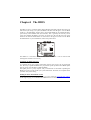
Chapter4 The BIOS
The BIOS is a piece of software (Basic Input Output System) that performs most low level
tasks. When you start up your system, the BIOS is the first code that gets to run. The BIOS
resides in a FLASH ROM, and the code in the FLASH ROM can be updated through a
special utility called AWDFLASH. (Award Flash). This is generally not necessary, but in
some cases updating the BIOS is necessary to support new devices that were not on the
market at the time the motherboard was released. For the physical location of the BIOS
FLASH ROM IC on your motherboard, refer to the picture below:
BIOS
The BIOS IC is inserted in an IC socket, which means that it can be removed and
exchanged for another IC if necessary.
Is updating my BIOS necessary?
As a general rule if your system is functioning properly and you are not an experienced
user, do not try to update the BIOS. Only if you have specific problems that a BIOS update
may solve may it be advisable to update the BIOS.
The update process is pretty complex, and you should bear in mind that if updating the
BIOS goes wrong you may render your system unbootable. Therefore, do not update unless
you know what you are doing.
Finding the latest official BIOS revision
For the latest official BIOS revision, please go to our website at www.lucky-star.com.tw.
On the support page you can find the latest BIOS files for our motherboards.
31
4-1
Updating the BIOS
As said, this procedure is complicated, only update your BIOS when you experience
problems with your system. Because each BIOS release completely overwrites the previous
version and there is no need to update to intermediate BIOS releases when updating the
BIOS. Therefore always use the latest BIOS revision when doing a BIOS update. The
BIOS update procedure is as follows:
In order to flash update the BIOS, you will need 2 files:
The BIOS binary file (.bin file from the website)
AWDFLASH.EXE utility file. (This utility can be downloaded from our website)
Create a directory on your C harddisk drive: and name it FLASH
Put the BIOS .bin file and the AWDFLASH utility in the FLASH directory.
You may want to jot the BIOS .bin file name down on a piece of paper.
Restart the computer, press DEL to go into the BIOS, then please disable the
following:
System BIOS Cacheable (in Advanced Chipset Features)
Video BIOS Shadow (in Advanced BIOS Features)
Save the changes by selecting ‘save and exit’, and restart the computer.
Press Ctrl + F5 just before Windows is starting up (right after the second BIOS
screen) for a DOS boot, you will see the message "Windows is bypassing all your
startup files". You end up at a DOS prompt.
Now type cd FLASH to change to the newly created directory.
Here type AWDFLASH mybios.bin /py /cc /sn /cd, where mybios.bin is the file name
for the BIOS binary file you want your BIOS to upgrade to. Now the upgrading will
begin.
WARNING:
STOP Do NOT in any way disturb the system during upgrading. If for any
reason the system is stalled your system may not be able to boot
again.
After the upgrading has ended press F1 to reset, press DEL to go into BIOS and make
the following changes:
Load Setup Defaults.
Go into the Frequency/Voltage Control page to adjust your CPU speed and voltage
(please make sure the CPU voltage matches your CPU specs, in case of doubts leave it
to ‘default’).
Save your settings and you are done.
32
4-2
The CMOS memory
The BIOS uses the CMOS memory to store all the settings that have been made through the
BIOS Setup pages.
Battery
The CMOS memory remembers all settings, even when the system is switched off, by use
of a 3V Lithium battery. If this battery runs low CMOS is unable to keep its settings and
you will need to replace the battery. The BIOS will give you an error message when it
detects a low battery voltage. The error message ‘CMOS checksum error’ may also point to
a low battery problem.
Restoring default settings
You can load default values into the CMOS memory by selecting ‘Load Optimized
Defaults’ in the BIOS Setup. If you need to force the CMOS settings to default without
entering the BIOS Setup page you can use the JP6 jumper. For the location of the jumper
and the battery, refer to the following picture:
BATTERY
BIOS
JP 6
33
Normally JP6 will be in the 1-2 position, this will connect the battery to the southbridge of
the chipset which contains the CMOS memory. If JP6 is temporarily set to 2-3 this will
interrupt the battery electricity flow, and the CMOS memory will be erased, this will
however only work if the power supply is not switched on. Now at the next reboot the
BIOS will automatically load the CMOS default values.
Take the following steps to clear CMOS memory:
Take the power cord from the power supply.
Temporarily set JP6 to 2 – 3, and set it back to 1 – 2.
Put the power cord back and restart the system, the default values will
be loaded.
CMOS Status
JP6
Retain CMOS settings
Clear CMOS Settings
CMOS
1 2 3
1 2 3
The following part of this chapter will describe the individual BIOS Setup pages and all the
items that can be adjusted to fine tune your system.
34
4-3
The BIOS Setup Pages
To enter the BIOS Setup pages, thke the following steps:
Start up the system.
After memory counting has finished, press [DEL] to enter the BIOS Setup
pages.
Now the following menu will appear:
CMOS SETUP UTILITY Copyright © 1984 – 2001 Award Software
" Standard CMOS Features
" Frequency/Voltage Control
" Advanced BIOS Features
Load Fail-Safe Default
" Advanced Chipset Features
Load Optimized Defaults
" Integrated Peripherals
Set Supervisor Password
" Power Management Setup
Set User Password
" PnP/PCI Configurations
Save & Exit Setup
"PC Health Status
Exit Without Saving
Esc : Quit
F9: Menu in BIOS
↑ ↓ → ← : Select Item
F10 : Save & Exit Setup
Time, Date, Hard Disk Type . . .
Selecting items
To Select items, use the following method:
Use the arrow keys to move between items and select fields.
Press [enter] to enter the selected submenu.
Submenus
All items that start with a " are submenus. Pressing [enter] when a submenu is
selected will enter that submenu.
Modifying selected items
The [Up]/[Down] keys can be used to modify values within the selected fields.
Note that some fields also let you enter values directly.
35
Hot Keys
Throughout the BIOS Setup Pages the hot keys will give you access to a group of
commands. Refer to the following table for the hot keys and their function:
Key
F10
[Esc]
F1
F2
F5
F7
Command
Save & Exit Setup
Quit
Help
Help
Previous values
Description
Saves the changes made and reboots the system.
Returns to the previous menu
General Help
Help for specific item
Restores the previous values. These are the values that the
user started the current session with.
Loads all options with the Optimized Default values.
Optimized Defaults
Save & Exit Setup
When you select the [SAVE & EXIT SETUP] option from the Main Menu, all
changes that you made will be saved to the CMOS memory and the setup utility
will exit, rebooting your system.
CMOS SETUP UTILITY Copyright © 1984 – 2001 Award Software
" Standard CMOS Features
" Frequency/Voltage Control
" Advanced BIOS Features
Load Fail-Safe Default
" Advanced Chipset Features
Load Optimized Defaults
" Integrated Periph
" Power Manag
Save to CMOS and Exit (Y/N)?
r password
word
" PnP/PCI Conf
Save & Exit Setup
" PC Health Status
Exit: Without Saving
Pressing [Y] and [enter] will save the changes, pressing [N] and [enter] will keep
the old settings.
36
Exit Without Saving
Selecting ‘Exit Without Saving’ will exit Setup without saving changes to CMOS.
CMOS SETUP UTILITY Copyright © 1984 – 2001 Award Software
" Standard CMOS Features
" Frequency/Voltage Control
" Advanced BIOS Features
Load Fail-Safe Default
" Advanced Chipset Features
Load Optimized Default
" Integrated Periphral
" Power Manag
Quit without Saving (Y/N)?
r Password
sword
" PnP/PCI Conf
Save & Exit Setup
" PC Health Status
Exit: Without Saving
Pressing [Y] and [enter] will Exit without saving, pressing [N] and [enter] will not Exit.
37
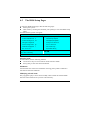
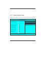
4-3-1 Standard CMOS Setup
Select the [STANDARD CMOS SETUP] option from the Main Menu and press [Enter]
key.
CMOS SETUP UTILITY Copyright © 1984 – 2001 Award Software
Standard CMOS Features
Date (mm:dd:yy)
Mon, Aug 18, 2001
Time (hh:mm:ss)
11 : 51 : 58
" IDE Primary Master
" IDE Primary Slave
" IDE Secondary Master
" IDE Secondary Slave
Press Enter None
Drive A
Drive B
1.44M, 3.5 in.
None
Video
Halt On
EGA / VGA
All,Errorsd
Item Help
Menu Level "
Base Memory:
Extended Memory:
Total Memory:
Press Enter None
Change the day, month, year and Century
Press Enter None
Press Enter None
640K
31744K
32768K
↑ ↓ → ← : Move
Enter: Select
+ / - / PU / PD: value
F10: save
ESC: Exit
F5 : Previous Values
F6:Fail-Safe Defaults
F7: Optimized Defaults
F1: General Help
This screen allows you to change the basic CMOS Settings such as date and time,
harddisk type etc. After you have made the changes you need to make press
[ESC] to return to the main menu.
Date and Time
Date
Time
Default
Weekday, month,
day ,year
hh:mm:ss
Possible Settings
Type the current date.
(weekday auto changes)
Type the current time
38
Notes
Using the P-Up / P-Dn keys to
toggle is possible
24-hour clock format. (15:15:00
= 3:15:00)
IDE Devices
When you select one of the IDE devices, a submenu will pop up. Refer to the
picture below.
CMOS SETUP UTILITY Copyright © 1984 – 2001 Award Software
IDE xxxx
IDE HDD Auto Detection
Press Enter
IDE Primary Master
Auto
Access Mode
Auto
Capacity
0 MB
Cylinder
Head
Precomp
Landing Zone
Sector
0
0
0
0
0
Item Help
Menu Level " "
To auto-detect the HDD’s size, head… on this
channel
This Menu is the same for all 4 IDE devices:
Primary Master IDE 1 first device
Primary Slave IDE 1 second device
Secondary Master IDE 2 first device
Secondary Slave IDE 2 second device
Values
Meaning
IDE HDD
Pressing Enter will make the BIOS auto detect the IDE device
Auto
Press Enter on this channel. The result will be displayed below, starting
Detection
with the ‘capacity’ item. (These items are read only)
Auto
This will auto detect the device at each boot up.
This will use the setting set by the user. No auto detection at
Manual
IDE xxx
start up will take place.
This setting means no device is present. This will prevent the
None
BIOS from looking for a device and speed up booting.
CHS
Selects the CHS access mode.
Logical Block Addressing, for HDD drives larger than 504MB
Access
LBA
(All modern HDDs)
Mode
Large
For very large HDDs.
Auto
The BIOS will automatically detect the best access mode.
39
Drive A and Drive B
The Drive A / B items allow you select the type of device that you have attached
to the Floppy (FDD1) connector on the motherboard. You can select between
different floppy disk drive types by using the Page-Up and Page-Down keys. If
you press [enter] while Drive A or B is selected the following menu will pop up
that will allow to choose a device as well:
Drive X
None
360K, 5.25 in.
1.2M, 5.25 in.
720K, 3.5 in.
1.44M, 3.5 in.
2.88M, 3.5 in.
…
...
…
…
…
…
[ ]
[ ]
[ ]
[ ]
[]
[ ]
↑ ↓ : Move Enter:Accept ESC: Abort
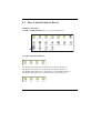
Video
The Video item allows you to select a video mode. Since most modes are outdated
we advise you to always select EGA/VGA. You can select between different
video modes by using the Page-Up and Page-Down keys. If you press [enter] a
menu pops up.
(Mono is for a monochrome screen that can only display one color)
Video
EGA/VGA
CGA 40
CGA 80
MONO
…
...
…
…
[ ]
[ ]
[ ]
[ ]
↑ ↓ : Move Enter:Accept ESC: Abort
40
Halt On
The BIOS will stop booting when an error is detected. You can set through this
item what errors will stop the system booting. You can select between different
error modes by using the Page-Up and Page-Down keys.
Halt On
Values
All Errors
No Errors
ALL, BUT
KEYBOARD
All, but
diskette
All, but
disk/key
Meaning
Stop booting on all errors.
Always Boot, no matter what error is detected.
Stop booting on all errors, but not on a keyboard error.
Stop booting on all errors, but a diskette error.
Stop booting on all errors, but keyboard and diskette errors.
41
4-3-2 BIOS Features Setup
Select the [Advanced BIOS Features] option from the Main Menu and press [Enter] key.
CMOS SETUP UTILITY Copyright © 1984 – 2001 Award Software
Advanced BIOS Features
X
X
Virus Warning
Disabled
CPU L1 & L2 Cache
Enabled
Quick Power On Self Test
Enabled
First Boot Device
Second Boot Device
Third Boot Device
Boot Other Device
Swap Floppy Drive
Boot Up Floppy Seek
Boot Up NumLock Status
Gate A20 Option
Typematic Rate Setting
Typematic Rate (Chars/Sec)
Typematic Delay (Msec)
Security Option
APIC Mode
MPS Version Control For OS
OS Select For DRAM > 64 MB
Report No FDD For WIN 95
Small Logo (EPA) Show
Floppy
HDD 0
LS 120
Enabled
Disabled
Disabled
On
Fast
Disabled
6
250
Setup
Item Help
Menu Level "
Allows you to choose the VIRUS warning
feature for IDE Hard Disk boot sector
protection. If this function is enabled and
someone attempt to write data into this
area,BIOS will show a warning message on
screen and clarm beep.
1.4
Non-OS2
No
Enabled
↑ ↓ → ← : Move
Enter: Select
+ / - /PU / PD: value
F10: save
ESC: Exit
F5 : Previous Values
F6:Fail-Safe Defaults
F7: Optimized Defaults
F1: General Help
The screen is not as long on your monitor. You can use the arrow keys to scroll down and
up the page. The following explains all individual items and their meaning.
42
Virus protection
Values
Virus
Warning
Enabled
Disabled
Meaning
The BIOS will give a beep and a warning whenever an attempt
is made to write to the boot sector of the HDD.
The BIOS will allow write attempts to the boot sector
CPU Cache settings
CPU L1 &
L2 Cache
Values
Disabled
Enabled
Meaning
Quick Power On Self Test
Values
Quick
Power On
Self Test
Enabled
Disabled
Meaning
The BIOS will execute test routines that test most parts of the
motherboard during boot up.
The BIOS will skip the tests, speeding up the boot process.
Errors will on the other hand not be detected.
Floppy Drive Settings
Values
Swap Floppy Enabled
Drive
Disabled
Boot-up
Floppy Seek
Enabled
Disabled
Meaning
This will swap floppy A and B. Most systems not even have 2
floppy drives, so this item is irrelevant .
Floppy A and B are not swapped
The BIOS will test whether the floppy has 40 or 80 tracks
during boot up. All new floppy drives are 80 tracks.
The BIOS will not test the amount of tracks.
Boot Devices
The first to third boot device items allow you to select what device the system should boot
from. If the BIOS fails to boot from the first boot device, it will attempt to boot from the
second boot device, if that fails too, the third boot device is tried. If you set the boot other
device item to enabled, the BIOS will try to boot from other devices if the first to third
choices all fail. If you set this item to disabled, the BIOS will not boot if the first to third
devices all fail to boot.
43
Values
Floppy
LS 120
HDD 0
SCSI
First ~ Third
boot device
CD-ROM
HDD1
HDD2
HDD3
ZIP100
LAN
Disabled
Meaning
The system attempt to boot from diskette.
(first boot device default)
The system will attempt to boot from an attached LS 120 drive.
(Third boot device default)
The system will attempt to boot from the first HDD.
(Second boot device default)
The system will attempt to boot from the first device attached to
the first SCSI interface.
The system will attempt to boot from the first CD-ROM found.
The system will attempt to boot from the second HDD.
The system will attempt to boot from the third HDD.
The system will attempt to boot from the fourth HDD.
The system will attempt to boot from an attached ZIP 100 drive
The system will attempt to boot over the network. You will
require a LAN card with boot BIOS for this option to function.
This disables booting from this device.
Keyboard Typematic Rate and Delay Settings
If you set the typematic rate setting item to disabled, the system will use the defaults of 6
and 250 for the rate and delay items. If you set it to enabled you can select the values
yourself. Refer to the table below:
Values
Meaning
This value sets the amount of time a character is repeated per
Typematic
6
~
30
second if it is kept down on the keyboard. Choose from the
Rate
following values: 6, 8, 10, 12, 15, 20, 24, 30.
This value sets the amount of time in ms before a character
Typematic
250
~
1000
starts repeating after it was pressed on the keyboard. Choose
Delay
from 250, 500, 750 and 1000 ms.
Security Option
The security option item allows you to select when the password needs to be entered. Refer
to the table below:
Values
Meaning
44
Security
Option
Setup
System
Password must be entered only when the user wants to enter the
BIOS setup.
The password must always be entered at boot.
OS Select for DRAM > 64MB
OS select for
DRAM >
64MB
Values
Non-OS2
Meaning
If your OS is not OS2, always select this setting.
OS2
Select this setting only if your OS is OS2
Report No FDD For WIN 95
Report No
FDD For
WIN 95
Values
Yes
Meaning
No
45
4-3-3 Chipset Features Setup
Select the [Advanced BIOS Features] option from the Main Menu and press [Enter] key.
CMOS SETUP UTILITY Copyright © 1984 – 2001 Award Software
Advanced BIOS Features
DRAM Timing Selectable
Item Help
CAS Latency Time
1.5
Active to Precharge Delay
7
DRAM RAS# to CAS# Delay
3
DRAM RAS# Precharge Time
3
DRAM Data Integrity Mode
Non-ECC
Memory Frequency For
Menu Level "
Dram Read Thermal Mgmt
System BIOS Cacheable
Video BIOS Cacheable
Video RAM Cacheable
Memory Hole At 15M-16M
Delayed Transaction
AGP Aperture Size (MB)
Delay Prior to Thermal
AGO Fast Write
BIOS Write In Flash
Disabled
Enabled
Disabled
Disabled
Disabled
Enabled
64
16Min
Enabled
Disabled
↑ ↓ → ← : Move Enter: Select + / - /PU / PD: value F10: save ESC: Exit F1: General Help
F5 : Previous Values
F6:Fail-Safe Defaults F7: Optimized Defaults
46
SDRAM Timing
If the DRAM Timing by SPD item is set to Enabled, the three items below will
automatically be set be the BIOS. To do this the BIOS will read information out of the SPD
EPROM that is located on the DIMM module, this information will tell the BIOS how to
best accesses the memory. If you set this item to disabled, you can set the memory access
items yourself. A word of warning though, if you are not familiar with DRAM settings
does NOT make any changes (for the sake of system stability). Refer to the table below for
the meaning of the individual DRAM items:
Values
Meaning
Normal
DRAM
Timing
The DRAM clock, DRAM Cycle Length, Bank Interleave
By SPD
Selectable
will automatically be set be the BIOS.
This is the default setting, always use this setting when the
1.5
system is unstable.
Use this setting only if your DIMM modules support CAS 2.
CAS Latency 2
Time
Use this setting only if your DIMM modules support CAS
2.5
2.5.
3
Use this setting only if your DIMM modules support CAS 3.
DRAM RAS#
to CAS#
Delay
DRAM RAS#
Precharge
Time
DRAM Data
Integrity
Mode
2
3
2
3
These controls the DRAM page miss and row miss lead off
timing.
SDRAM precharge time by RAS.
Non-ECC
ECC
Cacheable
Values
System BIOS Enabled
Cacheable
Disabled
Meaning
Define whether system BIOS area cacheable or not.
47
Video BIOS
Cacheable
Video RAM
Cacheable
Enabled
Disabled
Enabled
Disabled
To define whether video BIOS area cacheable or not.
To define whether video RAM area cacheabled or not.
Memory Hole
Some old devices need a memory hole to be present between 15M and 16M. CPU Cycles
matching the hole will be passed on to the PCI bus instead of accessing the memory.
Normally you can disable this setting, but if one of your devices needs it set it to enabled.
Values
Meaning
Memory Hole Disabled
There is no memory hole.
at 15M-16M Enabled
A memory hole exists between 15 and 16MB.
Delay Item
Values
Meaning
Enabled
Disabled
Delay Prior to 4, 8, 16, 32
Thermal
Min
Delay
Transaction
AGPAperture Size (MB)
Values
Meaning
4,
8,
16,
32,
On-Chip
Video
64, 128,
Window Size 256
Write Item
Values
Enabled
Disabled
BIOS Write In Enabled
Flash
Disabled
Meaning
AGP Fast
Write
48
4-3-4 Integrated Peripherals
Select the [Integrated Peripherals] option from the Main Menu and press [Enter] key.
CMOS SETUP UTILITY Copyright © 1984 – 2001 Award Software
Integrated Peripherals
Onchip Primary PCI IDE
Enabled
IDE Primary Master PIO
Auto
IDE Primary Slave PIO
Auto
IDE Primary Master UDMA
Auto
IDE Primary Slave UDMA
Auto
Onchip Secondary PCIIDE
IDE Secondary Master PIO
IDE Secondary Slave PIO
IDE Secondary Master UDMA
IDE Secondary Slave UDMA
USB Controller
USB Keyboard Support
USB Mouse Support
AC97 Audio
AC97 Modem
Init Display First
Onboard Audio
IDE HDD Block Mode
POWER ON Function
KB Power ON Password
Hot Key Power ON
Onboard FDD Controller
Onboard Serial Port 1
Onboard Serial Port 2
UART Mode Select
Enabled
Auto
Auto
Auto
Auto
Enabled
Disabled
Disabled
Auto
Auto
AGP
Enabled
Enabled
BUTTON ONLY
Enter
Ctrl-F1
Enabled
Auto
Auto
Normal
Item Help
Menu Level "
49
X
RxD , TxD Active
IR Transmission Delay
UR2 Duplex Mode
Use IR Pins
Onboard Parallel Port
Parallel Port Mode
EPP Mode Select
ECP Mode Select
PWRON After PWR-Fail
Game Port Address
Midi Port Address
Midi Port IRQ
Hi, Lo
Enabled
Half
IR-Rx2Tx2
378/ IRQ7
SPP
EPP1.7
3
Off
201
330
10
↑ ↓ → ← : Move Enter: Select + / -/ PU / PD: value F10: save ESC: Exit F1: General Help
F5 : Previous Values
F6:Fail-Safe Defaults F7: Optimized Defaults
The screen is not as long on your monitor. You can use the arrow keys to scroll up and
down the page.
IDE Channel Settings
The following table explains IDE channel settings and what they mean:
Values
Meaning
Onchip
Enabled
Enables the use of the first (primary) IDE channel.
Primary PCI
Disabled
IDE
Onchip
Enabled
Secondary
Disabled
PCI IDE
Auto
xxx PIO
xxx - UDMA
Mode 0
Mode 1
Mode 2
Mode 3
Mode 4
Auto
Disabled
IDE HDD
Block Mode
Enabled
Disabled
This will disable the use of the first (primary) IDE channel.
Enables the use of the secondary IDE channel.
This will disable the use of the secondary IDE channel.
The BIOS will assign a PIO mode to this device automatically
when appropriate
Select a PIO Mode here. PIO mode 0 is slowest, PIO mode 4 is
fastest, check your HDD to see what PIO mode it supports.If
your IDE device supports UDMA mode, then it best to enable
that mode since it is considerably faster than PIO mode. (Set to
auto for auto-detection)
The BIOS will automatically use Ultra DMA Mode if the IDE
device supports it.
This will disable the use of Ultra DMA for this device.
Block mode allows faster transfer of data between the system
and the HDD. Most modern HDDs support it.
Block Mode is not used.
USB Setting
50
USB
Controller
USB
Keyboard
Support
USB Mouse
Support
Values
Enabled
Disabled
Enabled
Meaning
This will allow use of a USB drive.
If you do not need a USB drive, set this item to disabled.
This will allow use of a USB keybaord.
Disabled
If you do not need a USB keyboard, set this item to disabled.
Enabled
This will allow use of a USB mouse.
Disabled
If you do not need a USB mouse, set this item to disabled.
Display Initialization
Values
Inie Display
First
PCI Slot
Onboard
Meaning
The BIOS will first search for a VGA adapter on the PCI bus, if
one is found it will be used as primary display.
The onboard AGP is first scanned.
Floppy Drive
Onboard
FDD
Controller
Values
Enabled
Meaning
This will allow use of a floppy drive.
Disabled
If you do not need a floppy drive, set this item to disabled.
AC97 Setting
Values
Enabled
AC97 Audio
AC97 Modem
Disabled
Meaning
This will allow use of a onboard AC97 sound codec.
If you do not need a onboard AC97 sound codec, set this item
to disabled.
Enabled
Disabled
Power On Function
Power On
Function
Values
Any Key
Button Only
Keyboard 98
Password
Hot Key
Meaning
Turn on power by click and key.
Only push power-on button.
Click with muti-media keyboard power-on
Power-on after key-in password (Must key-in password first).
Power-on by not key (must set hot-key first).
51
Mouse Lelt Power-on when mouse left key click
Mouse Right Power-on when mouse right key dick.
KB Power On
Enter
Password
Hot Key
Power On
Ctrl-F1~
Ctrl-F12
COM ports (Serial Ports)
Values
Auto
Disabled
Onboard
serial port 1 / 3F8/IRQ4
2
2F8/IRQ3
3E8/IRQ4
2E8/IRQ3
Meaning
The bios will automatically use serial ports.
If you do not need the serial port in question, set this item to
disabled.
Set an IO address and an IRQ to be used by serial ports.
IR Control
UART Mode
Select
UR2 Duplex
Mode
Values
Normal
IrDA
ASKIR
SCR
Half
Full
Meaning
Allows use of the IR port in IrDA mode.
Allows use of the IR port in ASKIR mode.
Allows use of the IR port in SCR mode.
Select if your IR device supports Half duplex only.
For IR devices that support full duplex.
Parallel Port (Printer Port)
Values
Disable
On board
3BC / IRQ7
Parallel Port 378 / IRQ7
278 / IRQ5
Parallel Port SPP
Meaning
Disables use of the parallel port.
Select an IO Address and an IRQ to be used by the parallel
port.
Enables use of SPP devices.
52
Mode
ECP mode
use DMA
EPP
Enables use of EPP devices.
ECP
Enables use of EPP devices.
ECP + EPP Enables use of ECP + EPP devices.
Select either DMA channel 1 or 3 (This is only relevant if ECP
1 or 3
was selected above). Default is channel 3.
PWRON After PWR-Fail
Values
Off
PWRON After
On
PWR-Fail
Former-Sts
Meaning
Default
Power-on when power-fail
If before power-fail is power-on (off) then turn on (off) PC
MIDI
Values
300
Midi Port
330
Address
Disabled
5
Midi Port IRQ
10
Meaning
Set mpu401 port address at 300.
Set mpu401 port address at 330.
Without midi port or none AC97 m/b
Set mpu-40 port IRQ address at 5.
Set mpu-40 port IRQ address at 5.
Game Port
Game Port
Values
201
209
Disabled
Meaning
Setting game port address at 201
Setting game port address at 209.
Disabled game port.
53
4-3-5 Power Management Setup
Select the [Power Management Setup] option from the Main Menu and press [Enter] key.
CMOS SETUP UTILITY Copyright © 1984 – 2001 Award Software
Power Management Setup
X
X
X
ACPI Function
Enabled
ACPI Suspend Type
Power Management
Video Off Method
Video Off In Suspend
Suspend Type
MODEM Use IRQ
Suspend Mode
HDD Power Down
Soft-Off by PWRBTN
CPU THRM-Throttling
Power On by Ring
USB KB Wake-Up Form S3
Resume by Alarm
Date(Of Month) Alarm
Time(hh: mm: ss) Alarm
S1 (POS)
User Define
DPMS
Yes
Disabled
3
Disabled
Disabled
Instant-Off
50.0%
Enabled
Disabled
Disabled
0
0
0
Item Help
Menu Level "
0
** Reload Global Timer Events **
Primary IDE 0
Disabled
Primary IDE 0
Disabled
Secondary IDE 0
Disabled
54
Secondary IDE 1
FDD, COM, LPT Port
PCI PIRQ[A-D]#
Disabled
Disabled
Disabled
↑ ↓ → ← : Move Enter: Select PU / PD / + / - : value F10: save ESC: Exit F1: General Help
F5 : Previous Values
F6:Fail-Safe Defaults
F7: Optimized Defaults
Values
Meaning
Enabled
Disabled
User Define The three items below can be set by the user
The three items below are set to: disabled, 1 hour, 1hour
Power
Min Saving
respectively.
Management
The three items below are set to: disabled, 1 min, 1min
Max Saving
respectively.
Will power down the HDD if it is idle for the amount of
HDD Power 1 – 15 Min
minutes selected here.
Down
Disabled
Will not power down the HDD.
Selecting a time will force the system into suspend mode after
1 Min to
Suspend
being idle for that time. Choose from the following time
1 Hour
Mode
intervals: 1, 2, 4, 6, 8, 10, 20, 30, 40 min and 1 Hour
Disabled
The system will never enter suspend mode.
ACPI
Function
Video Options
Video Off
Method
Values
Blank
Screen
V/H sync +
blank
Meaning
The screen will be blank (black) only.
The vertical and horizontal sync pulses will be stopped, and the
screen will be blank.
55
DPMS
If your monitor supports DPMS, it can be switched off through
support
that.
Video Off In Yes
Suspend
No
Stop Grant
Suspend Type PwrOn
Suspend
Modem IRQ
Modem Use
IRQ
Values
NA
3 - 11
Meaning
This disables the modem IRQ
Select an IRQ line that will be assigned to your modem here.
Choose from: 3 (default), 4, 5, 7, 9, 10, 11.
Power Button
Values
Meaning
Switches the system off immediately when pressing the power
Instant-off
Soft off by
button.
power button
This requires you to press the power button for at least 4
Delay 4 Sec
seconds before the system switches off.
Wake Events
Values
Wake-Up By Enabled
PCI Card
Disabled
Resume By Alarm
Values
Resume By
Alarm
Meaning
Allow the system to wake up on a PCI card IRQ.
Will not allow the system to wake up on a IRQ form a PCI card.
Disabled
Meaning
You can set the date and time on RTC (real-time clock) alarm
awaken a system which has been powered down.
Disabled this function.
Values
Meaning
Enabled
Date Setting
56
Date (of
Month)
Alarm/ Time
(HH:MM:SS)
You can set the date (of month) and timer (hh:mm:ss), any
event occurring will awaken a system which has been powered
down.
IDE
Primary
(Secondary )
IDE 0/1
Values
Enabled
Meaning
Enabled monitor Primary (Secondary) IDE 0/1 for Green event/
Disablec
Disabled this function.
FDD, COM, LPT Port
Values
FDD, COM, Enabled
LPT Port
Disabled
Wake Events
Values
PCI PIRQ
Enabled
{A-D}#
Disabled
Meaning
Meaning
4-3-6 PnP / PCI Configurations
Select the [PnP / PCI Configurations] option from the Main Menu and press [Enter] key.
CMOS SETUP UTILITY Copyright © 1984 – 2001 Award Software
PnP / PCI Configurations
X
Reset Configuration Data
Disabled
Resources Controlled by
Auto (ESCD)
IRQ Resources
Press Enter
PCI/VGA Palette snoop
Disabled
Item Help
Menu Level "
Default is Disabled. Select Enabled to reset
Extended System Configuration Data ESCD>
When you exit Setup if you have installed a new
add-on and the system reconfiguration has
Cause such a serious conflict that the OS
cannot boot
↑ ↓ → ← : Move Enter: Select + / - /PU / PD: value F10: save ESC: Exit F1: General Help
F5 : Previous Values
F6:Fail-Safe Defaults
F7: Optimized Defaults
57
Reset Configuration Data
Values
Disabled
Reset
Configuration
Data
Enabled
Meaning
This will not reset the system configuration data (IRQs, DMAs)
on reboot.
This will reset the configuration data. Remember to enable this
item every time you make a change to your system (such as
switching PCI cards etc).
Resources Controlled by
Values
Resources
Controlled
By
Manual
Auto
Meaning
The table will show the below items: “Reset Configuration
Data, IRQ-3 assigned to, DMA-0 assigned to.” The user can
adjust the shown items as required.
The table will not show the above items, and the system will
automatically assign the above setup.
Resources
If you set the Resources Controlled by item to Auto (ESCD), the BIOS will manage all
resources for you. If you set it to manual to two items below will allow you to assign the
resources manually.
Values
Meaning
PCI/ISA
This setting means the BIOS will assign the interrupt as needed.
IRQ-x
PnP
This means that it is not fixed to a device
assigned to
(x = 3 to 15) Legacy ISA If you need to make sure that a certain interrupt is assigned to
an ISA device, set that interrupt to legacy ISA.
DMA-x
PCI/ISA
This setting means the BIOS will assign the DMA Channel as
assigned to PnP
needed, it is not fixed to a device
(x = 0, 1, 3,
If you need to make sure that a certain DMA channel is
Legacy ISA
5, 6, 7)
assigned to an ISA device, set that channel to legacy ISA.
PCI / VGA Palette Snoop
PCI / VGA
Values
Disabled
Meaning
Default setting.
58
Palette
Snoop
Enabled
This will allow the system to look at the palette the VGA uses
to display. Some applications speed up with this setting but it is
mostly obsolete.
4-3-7 PC Health Status
Select the [PC Health Status] option from the Main Menu and press [Enter] key.
CMOS SETUP UTILITY Copyright © 1984 – 2001 Award Software
PC Health Status
CPU Warning Temperature
Disabled
Item Help
Current System Temp.
Current CPU1 Temperature
Menu Level "
Current CPUFAN1 Speed
Current CPUFAN2 Speed
Current CPUFAN3 Speed
CPU <U>
+ 3V
+ 5V
+ 12V
- 12 V
- 5
59
VBAT (V)
5VSB (V)
Shutdown Temperature
Disabled
↑ ↓ → ← : Move Enter: Select + / - / PU / PD: value F10: save ESC: Exit F1: General Help
F5 : Previous Values
F6:Fail-Safe Defaults F7: Optimized Defaults
CPU Warning Temperature
Values
Meaning
Disabled
CPU
50℃/ 122℉, 53℃/ 127℉, 56℃/ 133℉, 60℃/ 140℉, 63℃/ 145℉, 66℃/ 151
Warning
Temperature ℉, 70℃/ 158℉,
Values
Meaning
Disabled
Shutdown
Temperature 60℃/ 140℉, 65℃/ 149℉, 70℃/ 158℉, 75℃/ 167℉,
4-3-8
Frequency/ Voltage Control
Select the [Frequency / Voltage Control] option from the Main Menu and press [Enter]
key.
CMOS SETUP UTILITY Copyright © 1984 – 2001 Award Software
Frequency / Voltage Control
CPU Clock Radio
X8
Auto Detect PCI Clk
Enabled
Spread Specrurm
Disabled
CPU Clock
100MHz
Item Help
Menu Level "
↑ ↓ → ← : Move Enter: Select + / - / PU / PD: value F10: save ESC: Exit F1: General Help
F5 : Previous Values
F6:Fail-Safe Defaults F7: Optimized Defaults
CPU Clock Ratio
60
Values
CPU Clock
Ratio
Meaning
X8 ~ X23
Auto Detect PCI Clk
Values
Auto Detec
DIMM/ PCI
Clk
Enabled
Disabled
Meaning
If set to enabled the BIOS will detect the values for the PCI
clock.
If disabled, the BIOS will use the values set on this page and on
the Advanced Chipset Features page.
Spread Spectrum
Spread
Spectrum
Values
0.25%
0.50%
Disabled
Meaning
CPU Clock
CPU Clock
Values
Meaning
Min = 100
Max = 132
4-3-9 Passwords
The BIOS Setup program allows you to specify passwords in the Main menu. The
passwords control access to the BIOS during system startup. The passwords are not case
sensitive. In other words, it makes no difference whether you enter a password using upper
or lowercase letters. The BIOS Setup program allows you to specify two separate
passwords:
Supervisor password
User password.
The function of the supervisor password depends on the setting for the Security Option
item on the Advanced BIOS Features page. If set to System, the supervisor password must
be given every time the system boots, if set to setup, the password must be given only
when you want to enter the BIOS Setup.
61
The user password has the same functionality, with the only difference that anybody
logging in with the user password may only change the user password when entering the
BIOS Setup page. All other items in the BIOS Setup will be disabled (unchangeable).
When both passwords are disabled, anyone may access all BIOS Setup program functions.
Setting the password
To set the Supervisor password, select the Set Supervisor Password item in the main BIOS
Setup Menu. Now a dialog will pop up asking you to enter a password.
CMOS SETUP UTILITY Copyright © 1984 – 2001 Award Software
" Standard CMOS Features
" Frequency/Voltage Control
" Advanced BIOS Features
Load Fail-Safe Default
" Advanced Chipset Features
Load Optimized Defaults
" Integrated Peripherals
Set Supervisor Password
" Power Manag
Enter Password:
" PnP/PCI Conf
ord
up
Exit Without Saving
" PC Health Status
Now you can enter your password, after entering the password the menu will pop up again
and will ask you to reconfirm the password. After entering and pressing [enter] the
password will be stored to CMOS RAM and the password will be enabled.
Disabling the password
To disable the password, simply press [enter] without entering any other letters or numbers. This will
disable the password, the BIOS will tell you by displaying the following dialog:
CMOS SETUP UTILITY Copyright © 1984 – 2001 Award Software
" Standard CMOS Features
" Frequency/Voltage Control
" Advanced BIOS Features
Load Fail-Safe Default
" Advanced Chipset Features
Load Optimized Defaults
Set Supervisor Password
" Integrated Peripherals
" Power Manag
Password Disabled!!!
ord
" PnP/PCI Conf
Press any key to continue
up
Exit Without Saving
" PC Health Status
62
Password Unknown
If you forgot the password, you can clear the password by erasing the CMOS RAM. The
RAM data containing the password information is powered by the onboard button cell
battery. Please refer to the CMOS RAM section earlier in this chapter. After clearing the
CMOS memory, hold down <Delete> during bootup and enter BIOS setup to re-enter user
preferences.
Chapter 5
Appendix
5-1 Memory Map
Address range
00000-7FFFF
80000-9FBFF
9FC00-9FFFF
Size
512K
127K
1K
A0000-C7FFF
C8000-DFFFF
160K
96K
E0000-EEFFF
60K
Description
Conventional memory
Extended conventional memory
Extended BIOS data area if PS/2 mouse is
installed
Available for hi DOS memory
Available for hi DOS memory and adapter
ROMs
Available for UMB
63
EF000-EFFFF
4K
F0000-F7FFF
F8000-FCFFF
FD000-FDFFF
FE000-FFFFF
32K
20K
4K
8K
Video service routine for monochrome &
CGA adapter
BIOS CMOS setup utility
BIOS runtime service routine (2)
Plug and play ESCD data area
BIOS runtime service routine (1)
5-2 I/O Map
000-01F
020-021
022-023
040-05F
060-06F
070-07F
080-09F
0A0-0BF
0C0-0DF
0F0-0FF
1F0-1FB
278-27F
2B0-2DF
DMA controller (master)
Interrupt controller (master)
Chipset control registers. I/O ports
Timer control registers
Keyboard interface controller (8042)
RTC ports & CMOS I/O ports
DMA register
Interrupt controller (slave)
DMA controller (slave)
Math coprocessor
Hard disk controller
Parallel port 2
Graphics adapter controller
64
2F8-2FF
360-36F
378-37F
3B0-3BF
3C0-3CF
3D0-CDF
3F0-3F7
3F8-3FF
Serial port 2
Network ports
Parallel port 1
Monochrome & parallel port adapter
EGA adapter
CGA adapter
Floppy disk controller
Serial port-1
5-3 Time & DMA Channels Map
Time map:
Timer channel 0 system timer interrupt
Timer channel 1 DRAM refresh request
Timer channel 2 speaker tone generator
DMA channels:
DMA channel 0 available
DMA channel 1 onboard ECP (option)
DMA channel 2 floppy disk (SMC chip)
DMA channel 3 onboard ECP (default)
65
DMA channel 4 cascade for DMA controller 1
DMA channel 5 available
DMA channel 6 available
DMA channel 7 available
5-4 Interrupt Map
NMI:
non-maskable interrupt
IRQ(H/W):
0 system timer interrupt from timer 0
1 keyboard output buffer full
2 cascade for IRQ 8-15
3 serial port2
4 serial port1
5 parallel port 2
6 floppy disk (SMC chip)
7 parallel port 1
8 RTC clock
66
9 available
10 available
11 available
12 PS/2 mouse
13 math coprocessor
14 onboard hard disk (IDE1) channel
15 onboard hard disk (IDE2) channel
5-5 RTC & CMOS RAM Map
RTC & CMOS :
00 seconds
01 seconds alarm
02 minutes
03 minutes alarm
04 hours
05 hours alarm
06 day of week
07 day of month
08 month
09 year
0a status register a
67
0b status register b
0c status register c
0d status register d
0e diagnostic status byte
0f shutdown byte
10 floppy disk drive type byte
12 hard disk type byte
13 reserve
14 equipment type
15 base memory low byte
16 base memory high byte
17 extension memory low byte
18 extension memory high byte
19-2d
2e-2f
30 Reserved for extension memory low byte
31 reserved for extension memory high byte
32 date century byte
33 information flag
34-3f reserve
40-7f reserved for chipset setting data
5-6 ISA I/O Address Map
I/O Address (HEX)
I/O device
000 - 01F
020 - 03F
040 - 05F
060 - 06F
070 - 07F
080 - 09F
0A0 - 0BF
0C0 - 0DF
0F0 - 0FF
DMA Controller 1, 8237A-5
Interrupt Controller 1, 8259A
System Timer, 8254-2
8042 Keyboard Controller
real-time Clock/CMOS and NMI Mask
DMA Page Register, 74LS612
Interrupt Controller 2, 8259A
DMA Controller 2, 8237A-5
i486 Math Coprocessor
68
I/O Address (HEX)
I/O device
1F0 - 1F8
200 - 207
20C - 20D
21F
278 - 27F
2B0 - 2DF
2E1
2E2 - 2E3
2F8 - 2FF
300 - 31F
360 - 363
364 - 367
368 - 36B
36C - 36F
378 - 37F
380 - 38F
3B0 - 3BF
Fixed Disk Drive Adapter
Game I/O
Reserved
Reserved
Parallel Printer Port 2
Alternate Enhanced Graphic Adapter
GPIB Adapter 0
Data Acquisition Adapter 0
Serial Port 2 (RS-232-C)
Prototype Card
PC Network (Low Address)
Reserved
PC Network (High Address)
Reserved
Parallel Printer Port 1
SDLC, Bisynchronous 2
Monochrome Display and Printer Adapter
I/O Address (HEX)
I/O device
390 - 393
3A0 - 3AF
3C0 - 3CF
3D0 - 3DF
3F0 - 3F7
3F8 - 3FF
6E2 - 6E3
790 - 793
AE2 - AE3
B90 - B93
EE2 - EE3
Cluster
Bisynchronous 1
Enhanced Graphics Adapter
Color/Graphics Monitor Adapter
Diskette Drive Controller
Serial Port 1 (RS-232-C)
Data Acquisition Adapter 1
Cluster Adapter 1
Data Acquisition Adapter 2
Cluster Adapter 2
Data Acquisition Adapter 3
69
I/O Address (HEX)
I/O device
1390 - 1393
22E1
2390 - 2393
42E1
62E1
82E1
A2E1
C2E1
E2E1
Cluster Adapter 3
GPIB Adapter 1
Cluster Adapter 4
GPIB Adapter 2
GPIB Adapter 3
GPIB Adapter 4
GPIB Adapter 5
GPIB Adapter 6
GPIB Adapter 7
70
Chapter 6
6-1
Q&A
Errors Messages During Power On Self Test
During power on self test (post), BIOS will automatically detect the system
devices. Below is the question that users most often meet. The user may press
“Esc” key to skip the full memory test.
1. Beep sound
On power on, the system make beep sound to offer different messages. If the
system is configured correctly, it prompts a short beep to show device
configuration is done correctly. When VGA card and DIMM modules are not
plugged well, the system makes longer and constant beep sounds.
2. BIOS ROM checksum error
It indicates the checksum of the BIOS code is not right and system will always
halt on power on screen. Contact the dealer to exchange a new BIOS.
3. CMOS battery fails
It indicates the CMOS battery does not work. Contact the dealer to exchange a
new battery.
4. CMOS checksum error
It indicates the CMOS checksum is incorrect. Load the default values in BIOS to
solve this problem. This error may result from a weak BIOS, so exchange a new
BIOS if necessary.
5. Hard disk initialize
Please wait a moment…
Some hard drives require more time to initialize.
71
6. Hard disk install failure
The system can not find or initialize the hard drive controller or the drive. Check
if the controller is set correctly. If no hard disk is installed, “Hard drive
selection” must be set to “none.”
7. Keyboard error or no keyboard present
This means the system can not initialize the keyboard. Check if the keyboard is
plugged well and be sure no keys are pressed during power on self test.
8. Memory test fails
There will be more information to specify the type and location of the memory
error.
9. Primary master hard disk fail
The BIOS find an error in the primary master hard disk drive.
10. Primary slave hard disk fail
The BIOS finds an error in the primary slave hard disk drive.
11. Secondary master hard disk fail
The BIOS finds an error in the secondary slave master hard disk drive.
12. Secondary slave hard disk fail
The BIOS finds an error in the secondary slave IDE hard disk drive.
72