1
DIGITAL PHOTO FRAME IMPLEMENTATION ON FPGA SYSTEM WITH
EMBEDDED OS
PANG CHUN CHET
UNIVERSITI TEKNOLOGI MALAYSIA
DIGITAL PHOTO FRAME IMPLEMENTATION ON FPGA SYSTEM WITH
EMBEDDED OS
PANG CHUN CHET
A report submitted in partial fulfilment of the
requirements for the award of the degree of
Bachelor of Engineering (Electrical-Microelectronics)
Faculty of Electrical Engineering
Universiti Teknologi Malaysia
JUNE 2014
ii
I declare that this report entitled “Digital Photo Frame Implementation On FPGA
System With Embedded OS ” is the result of my own research except as cited in the
references. The report has not been accepted for any degree and is not concurrently
submitted in candidature of any other degree.
Signature
Name
Date
:
:
:
PANG CHUN CHET
June 22, 2014
iii
Dedicated, in appreciation for the support, understandings and encouragement to my
beloved parents, sister and brother.
iv
ACKNOWLEDGEMENT
First of all, I would like to take the opportunity to thank to University
Technology Malaysia for giving me the opportunity to utilize academic and practical
experiences in carrying out this final year project. Next, I would like to take the
opportunity to express my deepest gratitude to my supervisor, PM Muhammad Munim
Bin Ahamd Zabidi for constant encouragement and guiding me throughout the process
of this project. Also, I would like to thank my supervisor again for his support and lend
me the latest Arrow SoCKit Evaluation board to complete my project. I would also like
to thank our Vecad Lab Assistant for their co-operations, helps and lend me the Altera
DE2 development board for my project. Besides that, I would like to extend my sincere
gratitude to my seniors and my friends who had given me a lot of guidance and help
during the implementation of this project. I truly appreciate their technical advices and
concern throughout the process of this project. Then, I would like to thank my family
who always giving me full support during my academic years. I am appreciative I had
gained a lot of knowledge as well as problems solving skills throughout the project.
v
ABSTRACT
Nowadays, with the mass popularity of digital cameras and high-pixel camera
Smartphones, people are able to capture interesting things surrounding them. However,
most of the captured pictures are stored in the storage card; computer and only a small
part of the pictures are printed out. Few reasons people are seldom to print out their
pictures is cost printing is expensive and limitation of space to put the photo frame
in their living room. This report presents how to develop a simple embedded system
prototype of Digital Photo frame using FPGA technology. The development platforms
that were researched are the Altera DE2 development board and the Arrow SoCKit
Evaluation board. Qsys Integration tool in Quartus II was used to integrate the needed
peripheral into the digital photo frame system. The picture output for the digital photo
frame interface is driven from the VGA connector on the development boards. An
embedded operating system will be customized and port into the development board
to work together with the FPGA. The Linux kernel was added a custom frame buffer
driver to support the functionality of VGA at FPGA part. The open source picture
viewer was then installed in the embedded OS to speed up the prototyping time of
digital photo frame. The final result of this project shows that digital photo frame
works steadily under the FPGA development board and can display picture in slide
show mode on a VGA monitor.
vi
ABSTRAK
Kini, dengan populariti massa kamera digital dan Telefon pintar kamera
yang tinggi pixel, manusia boleh menangkap perkara yang menarik di sekeliling
mereka dengan mudah. Walau bagaimanapun, kebanyakan gambar-gambar yang
ditangkap disimpan dalam kad penyimpanan; komputer dan hanya sebahagian kecil
daripada gambar-gambar yang akan dicetak keluar. Antara sebab yang menyebabkan
kebanyakan orang jarang mencetak gambar-gambar mereka adalah kos percetakan
yang mahal dan had ruang untuk meletakkan bingkai foto di ruang tamu mereka.
Oleh itu, kemunculan bingkai foto digital menyediakan manusia dengan pilihan yang
baik. Laporan ini akan membentangkan membangunkan sistem prototaip mudah
bagi bingkai foto digital menggunakan teknologi FPGA. Platform pembangunan
yang dikaji adalah Altera DE2 Development Board dan Arrow SoCKit Evaluation
Board. Integrasi sistem bagi bingkai foto digital projek ini telah dilakukan dengan
menggunakan alat Integrasi Qsys dalam Quartus II. Pengeluaran gambar untuk gambar
bingkai digital dipandu dari penyambung VGA di lembaga pembangunan. Satu sistem
operasi terbenam akan disesuaikan dan pelabuhan ke dalam lembaga pembangunan
untuk bekerja bersama-sama dengan FPGA itu. Linux kernel ditambah pemandu
penimbal bingkai adat untuk menyokong fungsi VGA di bahagian FPGA. Sumber
terbuka gambar penonton kemudian dipasang di OS terbenam untuk mempercepatkan
masa prototaip bingkai foto digital. Hasil akhir projek ini menunjukkan bahawa
bingkai foto digital mampu beroperasi dalam keadaan yang baik di bawah lembaga
pembangunan FPGA dan boleh memaparkan gambar dalam mod pertunjukan slaid
pada monitor VGA.
vii
TABLE OF CONTENTS
CHAPTER
TITLE
DECLARATION
DEDICATION
ACKNOWLEDGEMENT
ABSTRACT
ABSTRAK
TABLE OF CONTENTS
LIST OF TABLES
LIST OF FIGURES
LIST OF ABBREVIATIONS
LIST OF APPENDICES
PAGE
ii
iii
iv
v
vi
vii
x
xi
xiii
xiv
1
INTRODUCTION
1.1
Background
1.2
Problem Statement
1.3
Research Objective
1.4
Scopes of Project
1.5
Outline of Thesis
1
1
2
2
2
3
2
LITERATURE REVIEW
2.1
Altera SOPC system used electronic digital photo
frames
2.2
Digital photo frames
2.3
Multi-Functional Digital Albums
2.4
A modularized FPGA-Based Embedded System
Development Platform
2.5
FPGA
2.6
FPGA Architecture
2.7
FPGA Design Flow
4
4
5
6
7
9
10
11
viii
2.8
2.9
3
4
5
Rapid Prototyping of Embedded Systems using
FPGA
FPGA Design Advantages
12
14
METHODOLOGY
3.1
Introduction
3.2
Tools Used
3.2.1
Quartus II and Embedded Design Suite
(EDS)
3.2.2
Altera DE2 Development Board
3.2.3
Arrow SoCKit Evaluation Board
3.3
Implementation of system on Altera DE2 Development Board
3.3.1
System architecture
3.3.2
Embedded Operating System
3.3.3
Implementation of uClinux operating
system
3.3.4
Hardware system Integration
3.4
Implementation of system on Arrow SoCKit
Evaluation Board
3.4.1
System architecture
3.4.2
Implementation of Linaro linux operating
system
3.4.2.1 Building Linux kernel
3.4.2.2 Linaro Root File System
3.4.2.3 Preloader and U-Boot Customization
3.4.2.4 Boot the Linux System
3.4.3
Hardware system Integration
15
15
15
RESULTS AND DISCUSSIONS
4.1
Altera DE2 Development Board Implementation
Result
4.2
Arrow SoCKit Evaluation Board Implementation
Result
36
CONCLUSION
5.1
Conclusion
47
47
16
16
17
19
19
20
21
24
26
26
28
28
30
30
32
34
36
41
ix
5.2
Future Works and Recommendations
47
REFERENCES
49
Appendix A
51
x
LIST OF TABLES
TABLE NO.
3.1
3.2
3.3
3.4
TITLE
Comparison of operating system for the Altera Development
Board
Files created
Description of the different boot stages
HPS BOOTSEL and CLKSEL setting
PAGE
20
29
31
32
xi
LIST OF FIGURES
FIGURE NO.
2.1
2.2
2.3
2.4
2.5
2.6
2.7
2.8
2.9
2.10
3.1
3.2
3.3
3.4
3.5
3.6
3.7
3.8
3.9
3.10
3.11
3.12
3.13
3.14
3.15
3.16
TITLE
Digital photo frame implemented on Altera DE2-70 board
and a 4.3 inch Terasic touch screen LCD
Nexys 2 FPGA and a VGA monitor used to implement a
digital photo frames
Architecture overview
Multi-Functional Digital Album
Design Concept:
(a) FPGA Core Module Board;
(b)Peripheral Module Board ; and (c) Integrated Platform
Implementation of digital photo frame on modularized FPGA
platform
Overview of FPGA architecture
Design Flow of FPGA
Time-to-market and market window
FPGA Vs ASICs design cycle
Altera DE2 Development board
Arrow SoCKit Evaluation Board
Bottom view of SoCKit Board
System Architecture using Altera DE2 Board
Platform selection
Kernel Customization
ISP 1362 setup fail
original code of ISP1362
Modified ISP 1362 code
Hardware design
Hardware system integration
System Architecture using Arrow SoCKit Board
Design steps
Typical Boot Flow
Preloader Overview
BOOTSELECT and CLOCKSELECT jumpers setting
PAGE
5
5
6
7
8
9
10
11
12
14
17
18
18
19
22
22
23
24
24
25
26
27
27
30
31
32
xii
3.17
3.18
3.19
3.20
3.21
4.1
4.2
4.3
4.4
4.5
4.6
4.7
4.8
4.9
4.10
4.11
4.12
4.13
4.14
4.15
4.16
4.17
4.18
FPGA Configuration Mode Switch
Putty Interface
Reboot button
Qsys part1
Qsys part2
Full compilation
zImage file
uClinux Operating System
USB mass storage detection
mount the USB storage content
Fail to open picture
nano-x closed unexpectedly
Full compilation
Block Diagram
Preloader and U-Boot
Kernel compilation
Kernel compiles successfully
Original picture
Zoom in picture
Zoom out picture
Rotated picture
128x64 dots LCD
Logo of digital photo frame
33
33
34
35
35
36
37
38
39
39
40
40
41
41
42
42
43
44
44
45
45
46
46
xiii
LIST OF ABBREVIATIONS
FPGA
–
Field Programmable Gate Array
SoC
–
System-On-a-Chip
IP
–
Intellectual Property
JPEG
–
Joint Photographic Experts Group
HDL
–
Hardware Description Language
ASIC
–
Application Specific Integrated Circuits
CLB
–
Configurable Logic Blocks
NRE
–
Non Recurring Expenses
IDE
–
Integrate Development Environment
SOPC
–
System on a Programmable Chip
OS
–
Operating Systems
USB
–
Universal Serial Bus
OTG
–
On-The-Go
HD
–
High Definition
HPS
–
Hard Processor System
VGA
–
Video Graphics Array
LCD
–
Liquid-Crystal Display
xiv
LIST OF APPENDICES
APPENDIX
A
TITLE
Top-level design entity verilog code
PAGE
51
CHAPTER 1
INTRODUCTION
1.1
Background
Ever since photographs were invented, the picture frame was used to display
photos prominently. However, the conventional photo frame has some limitations.
Firstly, the space constraint, only a limited number of photo frames can place in our
living room. Secondly, the photos can get tarnished over the years due to environmental
conditions.
Hence the digital photo frames was introduced to overcome the limitations
of the traditional picture frame. A digital photo frame is basically an LCD display
that displays photo without the need of a computer or printer, which mean that we
can display collection of our favorite photos on a single location. Also, there is
no risk of the image being destroyed by environmental factors, because the photos
are digital. Digital photo frames also can provide great opportunities for increasing
social interactions in the home that will improve the experience of people’s lives by
supporting and increasing the emotional connections among them.
This project aims to implement a digital photo frames using fieldprogrammable gate array (FPGA) System-on-a-Chip Technology. The implementation
can be divided into hardware and software parts. Two different development platforms
were used to achieve the objectives of this project, that is Altera DE2 development
board and Arrow SoCKit Evaluation Board. Integration tools was used to integrate
the needed components in hardware part, such as VGA output and USB devices.
On the software part, the Linux platform was used to build the digital photo frame
application as Linux has strong support for different architectures especially for the
ARM architecture.
2
1.2
Problem Statement
The System-on-Chip (SoC) technology on FPGA is still new and not many
people understand it. FPGA implementation of SoC enables the integration of
Intellectual Property (IP) from different sources to rapidly build an embedded system.
FPGAs are reconfigurable meaning that products can be developed and marketed in a
short time. Therefore, understanding the SoC knowledge is important in order for us
to implement any embedded product in the future.
To gain an understanding of the SoC design process, the digital picture frame
was used as a case study.
Most of the commercial digital photo frame available on the market today has
a single function. By exploring the SoC design options, the digital picture frame offers
an expandable platform which can support new features such as face detection, motion
detection and video playback.
1.3
Research Objective
There are 3 objectives of this project:
1.
To learn and understand SoC technology on FPGA.
2.
Prototype a digital photo frame on FPGA for hardware verification and early
software development.
3.
To implement a user friendly digital photo frame that can used by everyone.
1.4
Scopes of Project
In order to achieve the objective of the project, there are several scopes had
been outlined:
1.
The Altera DE2 Development Board and Arrow SoCKit Evaluation Board were
used.
3
2.
The application was developed using C/C++ and Verilog Hardware Description
Language.
3.
Open source picture viewer that can support a wide range of image formats,
including JPEG, PNG, Bitmap, and TIFF. The main format of the image was
used throughout this project is JPEG (Joint Photographic Experts Group).
1.5
Outline of Thesis
This report consists of five chapters and each chapter will be briefly discussed
here. Chapter 1 will give an overview of this digital photo frame project. The project
background, the problem statement, project objective, scope of the project and project
outline will be included in this chapter.
The next chapter, which is chapter 2, will be focusing on the previous works
that have done by other researchers, some FPGA theory and SoC embedded system
knowledge. It will be discussed on the various types of techniques and methods to
implement a digital photo frame prototype.
Besides that, chapter 3 describes the details on the methodology of this project.
This project consists of three layers, which is FPGA system hardware, embedded
Linux and user space application program. Next, this chapter will explain the steps
and methods to install an embedded OS into the development boards. The explanation
of the hardware design will be discussed here also.
Next, Chapter 4 is discussing about the result obtained for this project. Then,
some discussions on the results of the project will be included in this chapter also.
Finally, Chapter 5 discusses the conclusion based on the result obtained for
this digital photo frame project. Then, some comment and suggestions for the future
improvement will be provided in this chapter.
CHAPTER 2
LITERATURE REVIEW
This chapter covers what have been done on some other researcher projects
and prototype of digital photo frames. Some of the components and design are being
considered when designing my project of digital photo frames using FPGA.
2.1
Altera SOPC system used electronic digital photo frames
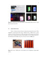
Figure 2.1 shows the prototype of digital photo frame created by two students
from Feng Chia University China [1]. They use the Altera DE2-70 ( Cyclone II
EP2C70F896C6N ) board as their development platform and a 4.3 inch touch screen
LCD to display the digital photo. This development board equipped with almost
70,000 logic elements and offers a rich set of features that make it suitable to be used
for the development of any sophisticated digital systems.
This digital photo frame can perform two image features, which is the negative
image extraction and the gray level slicing function. The on board button on DE270 board was configured as user interface for user to control the digital photo frame
such as forward or backward the picture on the screen. Besides, the touchscreen LCD
enables the user to change the picture on the screen by just touching the screen. Users
can easily access various components on the DE2 board from their host computer using
the control panel facility software provided by Altera. Altera DE2 control panel was
utilized to transfer the image file from computer to DE2 board flash memory. Image
file was then decoded and display on the LCD screen.
5
Figure 2.1: Digital photo frame implemented on Altera DE2-70 board and a 4.3 inch
Terasic touch screen LCD
2.2
Digital photo frames
Figure 2.2 shows the project done by students from Lund University [2]. They
implement a digital photo frame using a Digilent Nexys 2 FPGA board, a VGA
monitor, on board push button and an SD card reader module plugged into the FPGA
board. The development environment of Xilinx EDK was used to complete the project.
The Xilinx Spartan 3E FPGA chip was used and it consists of 500K gates.
Figure 2.2: Nexys 2 FPGA and a VGA monitor used to implement a digital photo
frames
6
The digital photo frames were used a part of image buffer on the VGA
controller due to memory size constraints on the Digilent Nexys 2 FPGA. SDRAM
memory will be used to hold the VGA buffer contents. On board buttons was
implemented as controller to control the functions of digital photo frame such as resets
the entire board, start or stop a slide show of images, forward and backward the images
on the screen. Besides, C code was implemented in the SD card module to enable the
FPGA board to read the image file from the SD card and display it on the VGA monitor.
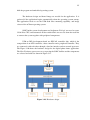
Figure 2.3 shows the digital photo frame architecture designed by Lund
University’s students. The software running on the MicroBlaze CPU will load a
predefined image from the SD card and write it to the 16MByte Micron SDRAM.
The CPU will just run an idle loop after completed loading the image and waits for
interrupts from the VGA controller. The interrupt routine fetches one row from the
SDRAM and writes it to the BRAM buffer in the VGA controller at each time the
interrupt received from the VGA controller. At the VGA controller side, interrupts are
sent when the end of the visible scan line is reached.
Figure 2.3: Architecture overview
2.3
Multi-Functional Digital Albums
Figure 2.4 shown is the multi-functional digital album created by students from
the Information Science institute, Beijing Jiaotong University [3]. The digital album
was implemented using an Altera DE1 FPGA board and a 5.7 inches LCD screen. This
development board consists of an Altera Cyclone II 2C20 FPGA chip with 20000 logic
elements.
7
The multi-functional digital album designed by them able perform a lot of
functions like can play background music while viewing photos, digital watermark
embedding and extraction, digital photo editions and processing effects and digital
photo network transmission. This digital album was designed to read the image file
from the SD card. Therefore, the Avalon bus and the Nios II processor were used
to control the SD card data reading and writing. SOPC Buider’s powerful system
integration feature was used to shorten the design cycle as a stable hardware system
can be built in a short time.
An embedded operating system of uClinux was implemented to the Nios II
processor to realize the complexities function of digital albums. Then, software
application of this digital photo frame system was developed under Linux operating
system.
Figure 2.4: Multi-Functional Digital Album
2.4
A modularized FPGA-Based Embedded System Development Platform
A digital photo frame project was developed using modularized FPGA
(MorFPGA) platform. MorFPGA is comprised of FPGA Core Module board with
memory modules, and peripherals module board. An open source processor core,
LEON3 [4], which is a synthesizable VHDL model of 32-bit processor were used
to implement the project. The feature of the MorFPGA platform is “Modularization”
which enhances the expandability and configurability. Hence, users can develop other
projects by just stack the needed peripheral board on top of the basic FPGA Core
Module board.
Figure 2.5(a) shows the block diagram of the FPGA Core Module board which
consists of FPGA and its corresponding serial configuration device, JTAG, buttons, and
8
external memory modules. The memory module includes the memory components
such as SRAM, SDRAM, and NAND-flash. Figure 2.5(b) illustrates the peripheral
module, which includes switches, buttons, keypad, 7-segment display, LCD, RS232,
VGA, PS/2 and audio. Figure 2.5(c) shown is the result after the peripheral module
board is stacked on top of the FPGA core module board.
Figure 2.5: Design Concept: (a) FPGA Core Module Board; (b)Peripheral Module
Board ; and (c) Integrated Platform
This digital photo frame can support several image formats like JPEG, Bitmap
and PNG. In addition, music format like MP3 and WMA also supported by digital
photo frames. Five functions ware implemented on the digital photo frames, which is
auto play, zoom in, zoom out, next and previous mode. Figure 2.6 shows the digital
photo frame implemented using modularized FPGA platform.
9
Figure 2.6: Implementation of digital photo frame on modularized FPGA platform
2.5
FPGA
Field programmable Gate Arrays (FPGAs) are pre-fabricated silicon devices
that can be electrically programmed in the field to become any kind of digital circuit
or system. It can be programmed by the designer after manufacturing and during
designing. This is also known as on site programmable.
For low to medium volume productions, FPGAs provide cheaper solution
and faster time to market as compared to Application Specific Integrated Circuits
(ASIC) which normally require a lot of resources in terms of time and money to
obtain a first device [5]. The programming of the FPGA is done using Hardware
Description Language (HDL). The programmable logic blocks are called configurable
logic blocks and reconfigurable interconnects are called switch boxes. Logic blocks
can be programmed to perform complex combinational functions, or simple logic
like AND and XOR. In a majority of FPGA’s the logic blocks also include memory
elements, which can be as simple as a flip flop or as complex as complete blocks of
memory.
10
2.6
FPGA Architecture
FPGA architecture are variations of the Figure 2.7 shown, however the final
architecture depends on the seller. Essentially the architecture consists of Configurable
I/O blocks, Programmable Interconnects and Configurable Logic Blocks (CLB). It also
has a clock circuitry to drive the clock signals to each logic block. Also other resources
like ALU’s, Decoders and Memory may be available.
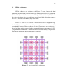
Figure 2.7 shown is an overview of FPGA architecture. Configurable logic
blocks (CLBs) are arranged in a two dimensional grid and are interconnected by
programmable routing resources, whereas I/O blocks are arranged at the periphery of
the grid and they are also connected to the programmable routing interconnect [5]. The
“programmable/reconfigurable” term in FPGAs indicates their ability to implement a
new function on the chip after its fabrication is complete.
Figure 2.7: Overview of FPGA architecture
11
2.7
FPGA Design Flow
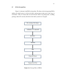
Figure 2.8 shown is the FPGA design flow. The flow of the design using FPGA
outlines the whole process of device design, and guarantees that none of the steps is
overlooked. Thus, it ensures that we have the best chance of getting back a working
prototype that will correctly function in the final system to be designed.
Figure 2.8: Design Flow of FPGA
12
2.8
Rapid Prototyping of Embedded Systems using FPGA
Figure 2.9 show time-to-market and market window. It shows the trend of the
life cycle of embedded product is becoming increasing smaller.
This situation will lead to new developments taking place more frequently to
replace the outdated products. In addition, the functionality and complexity of the
embedded system are rapidly increasing and this definitely will require more time and
manpower for the embedded system design cycle. The consumer demand for variety
functionality of a product directly increased the complexity of the embedded system on
a chip [6]. However, complexity gap was exists between the application requirements
and the capabilities of current silicon technologies.
Figure 2.9: Time-to-market and market window
Nowadays the demand for high complexity and variety functionality of an
embedded product is increasing day by day. But, the real world system-on-chip
(SoC) complexities were lagging behind the capabilities of the silicon hardware [7].
Therefore, rapid prototyping of embedded systems using FPGA may reduce the
complexity gap problems in order to satisfy the current trends in the embedded system
market. Rapid system prototyping using FPGA technology will allow the researchers
or engineers to discover the design errors as early as possible. In addition, other design
alternatives can be explored to give shorter development period. Rapid development of
13
prototypes definitely will satisfy the need of time to commercial the embedded system
product to the market.
Microcontrollers, microprocessors, ASICs and FPGAs can be used to develop
the embedded system. However, the FPGA can be considered as a powerful solution
to develop any kind of embedded system such as real time face detection applications
due to its reconfigurable characteristic. In general, the impact of FPGAs occurs not
only in the prototyping phase of development, but also the final stage of product
development. The difference between ASICs and FPGAs depends on costs, tool
availability, performance and design flexibility. FPGA design is more flexible due
to its reconfigurable characteristic, and the designer can easily change their design by
using the hardware description language (HDL). Whereas for the ASIC, it is not reprogrammable and thus cannot be changed after a certain point in the design process is
passed. Therefore, modifying or change the design of ASICs will need to go through
a long process of development.
Some large and complex embedded system using ASIC technique may take a
year or more to complete the design. Therefore, a good way to shorten development
time of an embedded system is to make prototypes using FPGAs at the beginning
stages and then switch to an ASIC. Prototype of the design can be implemented on
FPGA which could be verified for almost accurate results before implement it in an
ASIC.
From the Figure 2.10 shown, the design cycle for FPGA is much simpler
than ASIC design cycle. The simpler design of the FPGA is due to the available
software that can handle much of the routing, placement, and timing. Hence, manual
intervention is less. In addition, the FPGA design flow also eliminates the complex
and time-consuming floorplanning, verification of 2nd and 3rd order effect, timing and
analysis. Hence, developing rapid prototypes using FPGA technology is a good choice
as it has an efficient design cycle compare to others.
14
Figure 2.10: FPGA Vs ASICs design cycle
2.9
FPGA Design Advantages
1.
Faster time-to-market : FPGA design can develop in shorter time as it no need
layout, masks or other manufacturing steps.
2.
Lower Non Recurring Expenses (NRE) : FPGA tools are cheap or even free,
example like Quartus II free web edition software.
3.
Simpler design cycle : Software able handles much of the routing, placement,
and timing.
4.
More predictable project cycle : The FPGA design flow eliminates potential respins, wafer capacities.
5.
Reusability : Designs of system can easily change using Hardware Description
Language (HDL) code if any design faults was detected. Then program it to the
FPGA and test it again.
6.
Field Reprogram ability : The FPGA can be reprogrammed in a short period of
time, whereas an ASIC will take expensive cost, and more than 4-6 weeks to
make the same changes.
CHAPTER 3
METHODOLOGY
3.1
Introduction
This chapter will discuss the methods, tools, and software to develop the
digital photo frame prototype. Two different development platform was used to
implement the digital photo frame that is Altera DE2 development board and Arrow
SoCKit Evaluation Board. A VGA monitor was used to display the photos from the
development board.
There are three layers in this prototype digital photo frame system and the
development environment is as follows:
1.
Bottom layer: FPGA system hardware, e.g. Altera DE2 development board,
Arrow SoCKit Evaluation Board.
2.
Middle layer: Embedded linux, e.g. uClinux, linaro Linux.
3.
Top layer: User space application program.
3.2
Tools Used
There are several development tools are used to develop the prototype of digital
photo frame. These include the Integrate Development Environment (IDE) used for
hardware and software design, and the Linux operating system was used for software
development. Integrated Development Environment tools of QuartusII 9.1 and NiosII
9.1 were used to prototype digital photo frame on the Altera DE2 Development Board.
Whereas, for the SoCKit Evaluation Board, development tools of QuartusII 13.0sp1
and SOC EDS 13.0 was used.
16
The Ubuntu Linux operating system was installed on the Oracle VM
VirtualBox to speed up the prototyping time. VirtualBox is a cross-platform
virtualization application that enable us to extend the capabilities of our existing
computer so that it can run multiple operating system at the same time.
3.2.1
Quartus II and Embedded Design Suite (EDS)
Altera Quartus II is a development tool produced by Altera. It is used for
analysis and synthesis of HDL design, which is used to compile the hardware design,
configure the target device with the programmer and perform timing analysis by clock
setting. The hardware description language that used to complete this project is Verilog
HDL coding.
QuartusII 9.1sp1 was used on the Altera DE2 development board as it has stable
performance and easy to used. In order to develop an embedded system of digital photo
frame on latest Arrow SoCKit Evaluation board, latest development tools of QuartusII
13.0sp1 are needed to complete the objective of this project.
Altera Nios II EDS is a comprehensive development package for Nios II
software design. It is automatically installed as part of the Quartus II software. In this
project, the Nios II EDS will be used to load the uClinux kernel into DE2 board. Altera
SoC Embedded Design Suite (EDS) is a comprehensive tool suite for the embedded
software development on Arrow SoCKit Evaluation board. It was used to develop the
application software part for this project.
3.2.2
Altera DE2 Development Board
This project will use the FPGA board with Cyclone II ( EP2C35F672C6 )
which consists of 35000 logic elements. This board consists of 8MB SDRAM, USB
port, VGA output, LCD display [8]. Hence, the image files are obtained through
the USB port, and decode through the open source picture viewer in the embedded
operating system before sending the image data to the frame buffer and display it on
VGA monitor screen. Figure 3.1 show the Altera DE2 board hardware platform.
17
Figure 3.1: Altera DE2 Development board
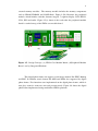
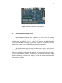
3.2.3
Arrow SoCKit Evaluation Board
Arrow SoCKit Evaluation Board combines the latest Cortex-A9 embedded
cores with industry-leading programmable logic, thus give engineers ultimate design
flexibility with unparalleled ease [9]. Altera SoC integrate an ARM-based hard
processor system (HPS) consisting of processor, peripherals, and memory interfaces,
with the FPGA fabric using a high-bandwidth interconnect backbone.
This board contains a powerful chip which integrates a 28nm Cyclone V FPGA
(5CSXFC6D6F31) with a ARM Cortex-A9 processor. The FPGA chip consists of
110K programmable logic elements. In addition, this board includes hardware such as
of two low-power DDR3 memory, a graphic LCD, MicroSD card slot, VGA output,
Ethernet networking, and much more. Figure 3.2 shows the Arrow SoCKit Evaluation
board hardware platform.
18
Figure 3.2: Arrow SoCKit Evaluation Board
Figure 3.3 shows the bottom view of SoCKit board.
Figure 3.3: Bottom view of SoCKit Board
19
3.3
Implementation of system on Altera DE2 Development Board
3.3.1
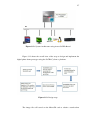
System architecture
At the beginning of the project, the Altera DE2 development board was used
to implement the digital photo frame prototype. The design of digital photo frame was
realized by the technique of SOPC based on Nios II soft-core processor. An embedded
operating system of uClinux was installed on the SDRAM of the FPGA board. The
problem with using an operating system on DE2 board is the memory concerns as its
uses most of the memory in the SDRAM, hence, the kernel size is needed for proper
customized in order to fix into the 8MB SDRAM.
Figure 3.4: System Architecture using Altera DE2 Board
The image could come directly from the computer via the RS232
communications. In order to develop a stand-alone embedded system, the USB flash
drive was decided upon to hold the image to be displayed on the VGA monitor. The
USB flash drive allows the user to store their favorite photos. This embedded system
was configured to detect and mount the USB pendrive. The use of an embedded
operating system can solve the USB driver implementation problem on DE2 board
and allow for a quick launch of a completed prototype. Embedded uClinux operating
system comes with a pre-installed open source image viewer called NxView and it
20
will be used to decode the image file from the USB pendrive and display it on a VGA
monitor.
The keyboard will be used as a controller to control the picture frame
application. This makes the application user friendly. During the design stage, the
JPEG type of image is considered to be displayed on the VGA monitor since it is most
common type of image which generated by most devices.
3.3.2
Embedded Operating System
The operating systems that are compatible with the Altera DE2 board are
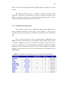
mostly commercial operating systems (OS) as seen in Table 3.1. Two types of
operating systems that are open source available on the market are eCos and uCLinux
[10].
Since, the Nios II processor does not include Memory Management Unit
(MMU) hardware, virtual addressing is not supported. The operating system required
is therefore is MMU-less and uses a flat memory addressing. Based on the Nios
II processor requirements and the application requirements the uCLinux embedded
operating system was chosen to be ported on the Cyclone II FPGA. In additions,
uClinux are considered due to its open source characteristics and availability of Nios
II IDE Plug-In.
Table 3.1: Comparison of operating system for the Altera Development Board
21
The original “micro-controller” Linux, uClinux was derived from the Linux
2.0 kernel and intended for microcontrollers like the Nios II processor that do not
have a Memory Management Unit [11]. The Nios II processor is ideal for running
the operating system. uClinux was first ported to the Motorola MC68328 DragonBall
Integrated Microprocessor. The first target system to successfully boot was a PalmPilot
device in 1998. Currently, uClinux includes kernel releases 2.0, 2.4, and 2.6 as well as
libraries and tool chains.
Recently work has been done on porting uCLinux to the Nios II processor. The
uCLinux project community develops patches and supporting tools for using Linux on
microcontrollers or embedded processors. The documentation is limited with regard
to the Nios II processor. There is a Nios forum (www.niosforum.org) that assists with
using uClinux on Nios.
The kernel of the operating system can be customized for a specific use.
Prebuilt kernels are available, but to decrease memory usage, custom kernels are very
effective.
The main features of the uClinux OS that are of great interest are:
1.
Mount command: used to mount/access different file systems including USB
flash drives
2.
NxView : Open source picture viewer to decode the image file and display it on
a VGA monitor.
3.3.3
Implementation of uClinux operating system
A Linux operating system is required to install, customize and build the
distribution of the uClinux Kernel, then using the command shell of Nios II to load
the uClinux OS into the Nios II processor.
The hardware design of the Nios processor has to be specified in order to
support uClinux. During the uClinux build process, the Nios hardware system file
(.sopc) is used to generate a list of peripheral names, addresses and IRQs. Many of the
device drivers within uClinux use hardcoded names for the peripheral being accessed.
22
Thus, designing a Nios II system to be compatible with uClinux, for Nios II, requires
that specific names be used for peripherals in the SOPC Builder. Failure to do this will
result in the loss of functionality when running the operating system.
The uClinux kernel image needs to be ported to the embedded processor. A
Linux kernel image is typically called a zImage. The hardware design of the embedded
processor and zImage are sent to the FPGA using a JTAG Uart cable and Nios II
Command Shell. The Figure 3.5 shows the interface to select the desired development
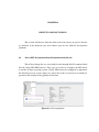
board in the Linux OS. Figure 3.6 shows the interface to customize the uClinux kernel.
Figure 3.5: Platform selection
Figure 3.6: Kernel Customization
23
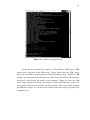
The source code of ISP1362 in uClinux kernel needed to modify in order the
USB port of the DE2 board able to detect the incoming USB devices. The Figure 3.7
shows that the ISP1362 can’t setup when uClinux OS was booted into the DE2 board.
Figure 3.8 shown is the original code of ISP1362.v come with the uClinux distribution
source. Figure 3.9 shows the ISP1362 was modified in order it can detect any incoming
USB devices.
Figure 3.7: ISP 1362 setup fail
24
Figure 3.8: original code of ISP1362
Figure 3.9: Modified ISP 1362 code
3.3.4
Hardware system Integration
The hardware design should at least consist of the main components needed
for the application. The components include a VGA controller, ISP1362 or USB
controller, and necessary memory to hold the program. The SDRAM was used to
25
hold the program and embedded operating system.
The hardware design and kernel image are needed for the application. It is
preferred if the application begins automatically when the operating system startup.
The application needs to use the USB flash drive mounting capability, and image
viewer of the uClinux operating system.
SOPC buider system development tool in Quartus II 9.1sp1 was used to create
32-bit Nios CPU, and automated Avalon switch fabric was used to form the total line
to connect the system together with peripheral components.
USB on DE2 development board use ISP1362 controller chip, which is the
composition of an OTG controller, a host controller and a peripheral controller. They
are connected with each other through a data bus interface and an external processor.
The Figure 3.10 shows the hardware design for the digital photo frame application.
The Nios II softcore processor was set up using the SOPC builder and the components
are selected and added as shown in Figure 3.11.
Figure 3.10: Hardware design
26
Figure 3.11: Hardware system integration
3.4
Implementation of system on Arrow SoCKit Evaluation Board
3.4.1
System architecture
Figure 3.12 shows the design architecture of digital photo frame using the
Arrow SoCkit Evaluation board. Custom FPGA peripheral will be added to the ARM
processor using Qsys system integration tool. Embedded Linux was used in this project
as it is freeware for all users. MicroSD card will be used to store the application system
and the image file. The open source picture viewer was used to decode the image file
before it’s able to display on the VGA monitor. The open source picture viewer was
used as it is free and can shorten the development time of the digital photo frame
prototype. The USB keyboard will be connected to the SoCkit board through the OTG
cable and act as the controller of digital photo frame, it can used to zoom in , zoom out
, rotate, and move forward or backward the image on a VGA monitor.
27
Figure 3.12: System Architecture using Arrow SoCKit Board
Figure 3.13 shows the overall view of the steps to design and implement the
digital photo frame prototype using the SoCKit Cyclone v platform.
Figure 3.13: Design steps
The image file will stored on the MicroSD card to obtain a stands-alone
28
embedded system. Once the SoCKit was powered on, the pictures were read from
the MicroSD card file system and decode to RGB format. The decoded image streams
are then sent via DMA to the Video IP chain within the FPGA before it’s sent to the
video output block. This SoCKit board contains 2gb DDR3 memory, hence a high
definition (HD) of JPEG picture was able to display on the VGA monitor.
This project will use both the HPS and FPGA portion of the SoC concurrently
to implement an embedded system. The embedded operating system was used to speed
up the development of prototypes.
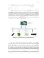
The picture output for the digital photo frame interface is driven from the VGA
connector on the SoCKit board. Altera’s Video IP suite was used to implement video
pipeline in the FPGA portion of the SoC. Open source picture viewer was installed in
the embedded OS to speed up the prototyping time of digital photo frame. The final
result of this project will show that digital photo frame work under SoCKit board and
can display picture in slide show mode on a VGA monitor.
3.4.2
Implementation of Linaro linux operating system
3.4.2.1 Building Linux kernel
Embedded kernel was compiled under the Ubuntu Linux operating system.
Stable Linux kernel version of 3.8 was download from the RocketBoards.org website.
1) Source was downloaded using command:
git clone git://git.rocketboards.org/linux.git
2) Archieve file of the source code was unpack and obtain a ‘linux’ directory.
Go into the ‘linux’ directory using command:
cd linux
3) A new branch was created from the remote arrow_sockit_vga using
command below:
29
git checkout –b neek_soc_38 origin/arrow_sockit_vga
4) PATH variable was set in the rightway to ensure the compile tool arm-linuxgnueabihf-gcc was available.
5) Following command was run to setup the build environment.
export ARCH=arm
export CROSS_COMPILE=arm-linux-gnueabihfexport LOADADDR=0x8000
6) Default configuration was import to enable new drivers.
make socfpga_defconfig
7) Command to start linux kernel compilation.
make uImage
8)Device tree was build in order to get the drivers to work.
make socfpga_cyclone5.dtb
Some of the files created after run the compilation are shown in Table 3.2.
Table 3.2: Files created
File
Description
vmlinux
Linux Kernel ELF file
arch/arm/boot/uImage
Linux Kernel image
arch/arm/boot/dts/socfpga_cyclone5.dtb
Device Tree Binary
30
3.4.2.2 Linaro Root File System
In order to get Linaro Linux build on Arrow SoCKit Evaluation board, Linaro
images are downloaded from the https://releases.linaro.org/13.04/ubuntu/quantalimages/nano. After unzip the tar.gz file, a binary folder will obtained. The linaro
rootfs are located in the binary subdirectory where the tar.gz file was extracted. The
following steps is follow to copy the Linaro Root Filesystem to the Linux partition.
1.
mount /dev/sdx2 /sdcard
2.
cp /binary /sdcard
3.
umount /sdcard
4.
sync
3.4.2.3 Preloader and U-Boot Customization
The Hard Processor System (HPS) boot starts when a processor is released
from reset (for example, power on the SoCKit board) and executes code in the internal
boot ROM at the reset exception address. The boot ROM contains software code that
executes after a reset button was pressed. The typical HPS boot flow was shown in
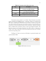
Figure 3.14. Description of the different boot stages are shown in Table 3.3.
Figure 3.14: Typical Boot Flow
31
Table 3.3: Description of the different boot stages
Stage
Description
BootROM
Performs minimal configuration and loads
Preloader into 64KB OCRAM
Preloader
Configure clocking, pinmuxing, DDRAM and
loads U-Boot into DDRAM
U-Boot
Configures FPGA, loads Linux kernel
Operating System
Applications development
The function of the preloader is user-defined. Typical functions of preloader
include initializing the SDRAM interface, configuring clocking and configuring the
HPS I/O pins. Initializing the SDRAM allows the preloader to load the next stage of the
boot software which is the open source boot loader, or known as U-boot. Preloader are
generated based on the handoff information folder from Quartus. Handoff information
folder is obtained when a hardware design is created and compiled in Quartus. The
Preloader is based on the Secondary Program Loader (SPL), which is a component of
U-Boot. The U-Boot responsible to loads the operating system and passes software
control to the operating system.
The Figure 3.15 shows an overview of Preloader is generated using the tools
provided with SoC EDS.
Figure 3.15: Preloader Overview
32
3.4.2.4 Boot the Linux System
There are few steps needs to follow in order to succesfully boot the embedded
Linux into the Arrow SoCkit board. Firstly, create Linux booting image file into
MicroSD card and then install the MicroSD card in the SoCKit board. SoCKit board
Bootsel jumpers (BOOTSEL[2:0]) are set as shown in Figure 3.16 to 101 for booting
from MicroSD card. Table 3.4 show the HPS BOOTSEL and CLKSEL setting on the
SoCKit board.
Figure 3.16: BOOTSELECT and CLOCKSELECT jumpers setting
Table 3.4: HPS BOOTSEL and CLKSEL setting
Board Reference
Signal Name
Setting
J15
CLKSEL0
Short Pin 2 and 3: Logic 0
J16
CLKSEL1
Short Pin 2 and 3: Logic 0
J17
BOOTSEL0
Short Pin 2 and 3: Logic 0
J18
BOOTSEL2
Short Pin 1 and 2: Logic 1
J19
BOOTSEL1
Short Pin 2 and 3: Logic 0
After that, MSEL jumpers ( MSEL[0:4] ) are set to 0000 and SW6 are set to 1
to enable the ARM processor to configure the FPGA and enable normal operation of
Linux. Figure 3.17 show the setting need to follow in order to boot the Linux OS into
SoCKit board.
33
Figure 3.17: FPGA Configuration Mode Switch
USB 2.0 OTG cable is used to connect the keyboard to the SoCKit board.
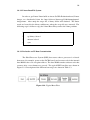
Connect a VGA monitor to the VGA connector of the SoCKit board. Putty terminal
was used to control the Linux on the SoCKit board. Putty also able to show the Linux
booting process and notify user which part was stuck when booting failed. Figure 3.18
show the Putty interface that can let user to control the Linux OS on the SoCKit board.
Figure 3.18: Putty Interface
34
WARM_RST button on the lower left corner of the socket board (KEY 6) was
used to rebooting the Linux once the button was being pressed. Figure 3.19 red circle
part show the WARM_RST button which acts as a reboot button.
Figure 3.19: Reboot button
3.4.3
Hardware system Integration
The hardware design should at least consist of the main components needed
for the digital photo frame application. The components include a VGA controller,
and necessary memory to hold the program. The MicroSD card memory was used to
hold the program and embedded operating system.
The hardware design and kernel image are needed for the application. Qsys
Integration development tool in Quartus II 13.0sp1 was used to include an ARM
processor, and other components into a stable system. Figure 3.20 and Figure 3.21
show the component included to build a system using Qsys Integration tool.
35
Figure 3.20: Qsys part1
Figure 3.21: Qsys part2
CHAPTER 4
RESULTS AND DISCUSSIONS
This section will discuss about the final result of my final year project. Results
are obtained in the hardware part and software part for two different development
platforms.
4.1
Altera DE2 Development Board Implementation Result
The uClinux image file was succesfully loaded through Nios II command shell
into the Altera DE2 FPGA board. Two steps are needed to configure the DE2 board
to run the uClinux operating system. Firstly, FPGA must be configured to implement
the Nios II processor system. Figure 4.1 shows the result of system was succefully be
generated and compiled using Quartus II software.
Figure 4.1: Full compilation
37
Secondly, kernel file was customized and compiled under the Linux platform
before download into SDRAM of Altera DE2 Development board. Nios II 9.1
command shell was used to load the embedded Linux operating system into the DE2
board. The Command Shell window is a Cygwin environment and is performed like the
Linux shell. Nios II command shell is a console window on the computer which was
used to explore uClinux once the uClinux had booted successfully in the DE2 board.
Standard Linux commands such as ls, cd, kill, ps can be used in uClinux. Figure 4.2
show the uClinux kernel file was successfully compiled under Linux platform.Figure
4.3 show an uClinux embedded operating system was successfully loaded into the DE2
board.
Altera DE2 board contain an 8MB SDRAM chip which will be used to store
the root file system, program memory and data memory, hence if too many processes
are running simultaneously, the kernel will run out of memory and crash.
Figure 4.2: zImage file
38
Figure 4.3: uClinux Operating System
Kernel file was customized to supports a VGA monitor, USB devices (USB
storage mass, keyboard) in the DE2 board. Figure below show the USB storage
mass was succesfully recognized under uClinux operating system. When the USB
pendrive was inserted into the USB port of the DE2 board, the uClinux will automatic
recognised it and display the details on the terminal. Figure 4.4 show the USB
mass storage detection on uClinux OS. Figure 4.5 shows the USB mass storage was
successfully mounted under uClinux operating system. After successfully mounted
the USB mass storage, we can list out the contents in the mass storage by using Unix
command of “ls”.
39
Figure 4.4: USB mass storage detection
Figure 4.5: mount the USB storage content
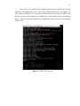
However, the picture was failing to display on the VGA monitor screen due
to some unknown reason and unknown bug in the open source picture viewer. Figure
4.6 show the pictures are failing to open in uClinux OS. Figure 4.7 show the nano-
40
X environment will closed unexpectedly when the NxView was executed to load the
picture from the USB pendrive.
Figure 4.6: Fail to open picture
Figure 4.7: nano-x closed unexpectedly
41
4.2
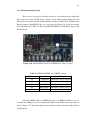
Arrow SoCKit Evaluation Board Implementation Result
The digital photo frame was successfully implemented on the SoCKit board.
Implementation was in software and hardware. Firstly, Quartus II 13.0sp1 software
are needed to build the system of the digital photo frame. Qsys integration tools will
be used to integrate the needed component like ARM processor, DMA frame buffer,
VGA output and other components into a system. After generating the system, top
entity Verilog code is created before running full Quartus compilation using Quartus
II 13.0sp1 software. Figure 4.8 show the full compilation was successfully run under
the Quartus II software. Figure 4.9 show block diagram of the created system under
Quartus II software.
Figure 4.8: Full compilation
Figure 4.9: Block Diagram
42
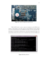
Figure 4.10 show the Preloader and U-Boot are able to work in the SoCkit
board and load the kernel image file.
Figure 4.10: Preloader and U-Boot
Figure 4.11 show the kernel start compiled under Linux platform when “make
uImage” command are typed. Figure 4.12 show the kernel image file are successfully
created and ready to use.
Figure 4.11: Kernel compilation
43
Figure 4.12: Kernel compiles successfully
Figure 4.13 show the final result of implementation digital photo frame using
Arrow SoCkit Evaluation board. Once the SoCKit board was powered on, the
application will start up automatically and searching the picture folder to display the
picture on the VGA monitor. In additions, slide show mode is enabled on this digital
photo frame application. The keyboard will be used as a controller for the digital photo
frame. Figure 4.14 shows the enlarged picture when “+” button on the keyboard being
pressed. Figure 4.15 shows the zoom out picture when “-” button on the keyboard
being pressed. Figure 4.16 shows the picture is rotated when “CTRL+R” button on the
keyboard being pressed.
44
Figure 4.13: Original picture
Figure 4.14: Zoom in picture
45
Figure 4.15: Zoom out picture
Figure 4.16: Rotated picture
Figure 4.17 shows the 128x64 dots LCD on SoCKit board will display “Digital
Photo Frame” when the application is startup.
46
Figure 4.17: 128x64 dots LCD
Figure 4.18 shows the logo created for this digital photo frame prototype. When
user power on the SoCKit board, this logo will appear in the VGA monitor left top area
before it start the digital photo frame application on embedded Linux.
Figure 4.18: Logo of digital photo frame
CHAPTER 5
CONCLUSION
In this chapter, all of the results of this project will be concluded here. In
addition, some future works and recommendations are also presented.
5.1
Conclusion
The main objective of this project was to prototype a digital photo frame using
FPGA board. This objective were successfully archieved at the end of the project. A
complete digital photo frame prototype was successful implemented on Arrow SoCKit
Evaluation board. Implementation was divided into hardware and software parts.
Digital photo frame hardware design system was built using Qsys integration tool.
For the software part, an embedded Linux operating system was used to speed up the
development time as it is free and have a strong support source from the internet. In
addition, the kernel is flexible and can be enhanced by embedded developers. The open
source picture viewer was successfully installed on embedded OS to display the image
file from the MicroSD card. At the end of the project, a stable digital photo frame
prototype was implemented which have ability to display photos automatically on the
VGA monitor screen with slide show mode once the SoCKit board are powered on.
5.2
Future Works and Recommendations
Although this project is considered successful, there are still many
improvements can be done in future time to optimize the performance of the digital
photo frame.
48
Below are the suggestions for the future improvement:
1.
Implement hardware JPEG decoder to reduce power.
2.
To integrate the motion detection function into the digital photo frame. This
function will be helping us save the power consumption in our house as if
no people’s motions are detected, then the digital photo frame will switch off
automatically and switch on if people’s motion are detected.
3.
To integrate a Wi-Fi function into the digital photo frame. This Wi-Fi function
will bring convenience to users as they can easily upload their picture into the
picture frame using a Wi-Fi connected smartphone.
4.
Accept hot-plug USB thumb drive and auto playback of all image files found on
thumb drive.
REFERENCES
1.
Zan, S. Z. and Hao, K. R. Altera SOPC system used electronic digital photo
frame. Feng Chia University. 2009.
2.
Olsson, M., Skanberg, S. and Eriksson, T. Digital Photo Frame. Lund
University. 2009.
3.
Hong, C., Deng, R. and Ye, Y. Multi-Functional Digital Albums Based on the
Nios II Processor. Beijing Jiaotong University. 2007.
4.
Chang, Y.-T., Huang, C.-M., Wu, C.-M., Chen, C.-Y., Lin, Y.-S., Kuo,
C.-T., Liu, T.-C. and Wey, C.-L. A modularized FPGA-based embedded
system development platform. IECON 2010-36th Annual Conference on IEEE
Industrial Electronics Society. IEEE. 2010. 1697–1702.
5.
Farooq, U., Marrakchi, Z. and Mehrez, H. FPGA Architectures: An Overview.
In: Tree-based Heterogeneous FPGA Architectures. Springer. 7–48. 2012.
6.
Hamblen, J. O., Hall, T. S. and Furman, M. D. Rapid prototyping of digital
systems: SOPC edition. Springer. 2007.
7.
Muralidharan, N. and Noel, A. The System on Chip Technology. Proceedings
of LACCEI, 2004. 4.
8.
Altera DE2 Board User Manual. URL ftp://ftp.altera.com/up/
pub/Webdocs/DE2_UserManual.pdf.
9.
Arrow SoCKit Evaluation Board User Manual.
URL http:
//www.rocketboards.org/pub/Documentation/
ArrowSoCKitEvaluationBoard/SoCKit_User_manual.pdf.
10.
Lariviere, D. and Edwards, S. A. uClinux on the Altera DE2. Columbia
University. 2008.
11.
uClinux-dist Developers Guide.
Armadillo.
2004.
URL http:
//download.atmark-techno.com/common/uclinux_dist_
developers_guide_en-1.1.pdf.
12.
Atitallah, A. B., Kadionik, P., Masmoudi, N. and Levi, H.
FPGA
implementation of a HW/SW platform for multimedia embedded systems.
50
Design Automation for Embedded Systems, 2008. 12(4): 293–311.
13.
Chu, P. P. Embedded SoPC Design with NIOS II Processor and Verilog
Examples. John Wiley & Sons. 2012.
14.
Daya, B. Rapid Prototyping Of Embedded Systems Using Field Programmable
Gate Arrays. Florida University. 2009.
15.
Devic, F., Torres, L. and Badrignans, B. Securing boot of an embedded linux
on FPGA. Parallel and Distributed Processing Workshops and Phd Forum
(IPDPSW), 2011 IEEE International Symposium on. IEEE. 2011. 189–195.
16.
Han, D. D., Zhang, T. C. and Zhang, J. Design and Implementation of
Intelligent Digital Photo Frame Based on FPGA. Applied Mechanics and
Materials, 2013. 380: 3296–3299.
17.
Kim, J. and Zimmerman, J. Cherish: smart digital photo frames for sharing
social narratives at home. CHI’06 Extended Abstracts on Human Factors in
Computing Systems. ACM. 2006. 953–958.
18.
Lu, Z., Zhang, X. and Sun, C. An Embedded System with uClinux based
on FPGA. Computational Intelligence and Industrial Application, 2008.
PACIIA’08. Pacific-Asia Workshop on. IEEE. 2008, vol. 2. 691–694.
19.
Paulose, L. and Cheedella, P. T. Enhancement of Digital Photo Frame
Capabilities With Dedicated Hardware. Ph.D. Thesis. 2012.
20.
RocketBoards.org, 2014. URL http://www.rocketboards.org/
foswiki/Main/WebHome.
21.
Williams, J. A. and Bergmann, N. W. Embedded Linux as a platform
for dynamically self-reconfiguring systems-on-chip. Ersa’04: the 2004
International Conference On Engineering of Reconfigurable Systems and
Algorithms. CSREA Press. 2004. 163–169.
22.
Yang, K.-p. and Beaubouef, T. A field programmable gate array media player
for realmedia files. Journal of Computing Sciences in Colleges, 2008. 23(6):
133–139.
23.
Wang, Z., Wei, Y. and Zhong, X. Embedded design based on the frame
buffer digital photo frame. Automatic Control and Artificial Intelligence (ACAI
2012), International Conference on. IET. 2012. 971–973.
APPENDIX A
TOP-LEVEL DESIGN ENTITY VERILOG CODE
A.1
Altera DE2 Board
module DPF (
CLOCK_50 ,
SW, / / t h e _ b u t t o n _ p i o
LEDR , / / t h e _ l e d _ r e d
KEY, / / t h e _ s w i t c h _ p i o
UART_TXD,
UART_RXD,
DRAM_DQ,
DRAM_ADDR,
DRAM_LDQM,
DRAM_UDQM,
DRAM_WE_N,
DRAM_CAS_N,
DRAM_RAS_N,
DRAM_CS_N,
DRAM_BA_0,
DRAM_BA_1,
DRAM_CLK,
DRAM_CKE,
SRAM_DQ,
SRAM_ADDR,
SRAM_UB_N,
SRAM_LB_N,
SRAM_WE_N,
SRAM_CE_N,
SRAM_OE_N,
52
OTG_DATA,
OTG_ADDR,
OTG_CS_N ,
OTG_RD_N ,
OTG_WR_N,
OTG_RST_N ,
OTG_FSPEED ,
OTG_LSPEED ,
OTG_INT0 ,
OTG_INT1 ,
OTG_DREQ0 ,
OTG_DREQ1 ,
OTG_DACK0_N,
OTG_DACK1_N,
TDI ,
TCK,
TCS ,
TDO,
VGA_CLK,
VGA_HS,
VGA_VS,
VGA_BLANK,
VGA_SYNC,
VGA_R,
VGA_G,
VGA_B,
);
input
CLOCK_50 ;
input
[3:0]
KEY;
input
[ 1 7 : 0 ] SW;
output
[3:0]
LEDR ;
output
UART_TXD ;
input
UART_RXD ;
inout
[ 1 5 : 0 ] DRAM_DQ;
output
[ 1 1 : 0 ] DRAM_ADDR;
output
DRAM_LDQM;
output
DRAM_UDQM;
output
DRAM_WE_N;
output
DRAM_CAS_N;
output
DRAM_RAS_N;
53
output
output
output
output
output
inout
output
output
output
output
output
output
inout
output
output
output
output
output
output
output
input
input
input
input
output
output
input
input
input
output
output
output
output
output
output
output
output
output
DRAM_CS_N ;
DRAM_BA_0 ;
DRAM_BA_1 ;
DRAM_CLK;
DRAM_CKE;
[ 1 5 : 0 ] SRAM_DQ;
[ 1 7 : 0 ] SRAM_ADDR;
SRAM_UB_N ;
SRAM_LB_N ;
SRAM_WE_N;
SRAM_CE_N ;
SRAM_OE_N ;
[ 1 5 : 0 ] OTG_DATA ;
[1:0]
OTG_ADDR;
OTG_CS_N ;
OTG_RD_N ;
OTG_WR_N;
OTG_RST_N ;
OTG_FSPEED ;
OTG_LSPEED ;
OTG_INT0 ;
OTG_INT1 ;
OTG_DREQ0 ;
OTG_DREQ1 ;
OTG_DACK0_N ;
OTG_DACK1_N ;
TDI ;
TCK ;
TCS ;
TDO;
VGA_CLK ;
VGA_HS ;
VGA_VS ;
VGA_BLANK;
VGA_SYNC ;
[9:0]
VGA_R ;
[9:0]
VGA_G;
[9:0]
VGA_B ;
54
a s s i g n OTG_FSPEED=1 ’ bz ;
a s s i g n OTG_LSPEED=1 ’ bz ;
wire
CPU_CLK ;
wire
CLK_18_4 ;
wire
CLK_25 ;
SDRAM_PLL PLL1
( . i n c l k 0 ( CLOCK_50 ) , . c0 (DRAM_CLK ) , . c1 ( CPU_CLK ) , . c2 ( CLK_25 ) ) ;
SocDPF S o c D P F _ i n s t (
. c l k _ 0 ( CLOCK_50 ) ,
. c l k ( CPU_CLK ) ,
. VGA_BLANK_from_the_vga_controller_0 (VGA_BLANK) ,
. V G A _ B _ f r o m _ t h e _ v g a _ c o n t r o l l e r _ 0 (VGA_B) ,
. V G A _ C L K _ f r o m _ t h e _ v g a _ c o n t r o l l e r _ 0 (VGA_CLK) ,
. V G A _ G _ f r o m _ t h e _ v g a _ c o n t r o l l e r _ 0 (VGA_G) ,
. V G A _ H S _ f r o m _ t h e _ v g a _ c o n t r o l l e r _ 0 (VGA_HS ) ,
. V G A _ R _ f r o m _ t h e _ v g a _ c o n t r o l l e r _ 0 (VGA_R) ,
. V G A _ S Y N C _ f r o m _ t h e _ v g a _ c o n t r o l l e r _ 0 (VGA_SYNC) ,
. V G A _ V S _ f r o m _ t h e _ v g a _ c o n t r o l l e r _ 0 (VGA_VS ) ,
. OTG_ADDR_from_the_ISP1362
(OTG_ADDR) ,
. OTG_CS_N_from_the_ISP1362
( OTG_CS_N_from ) ,
. OTG_DACK0_N_from_the_ISP1362
(OTG_DACK0_N ) ,
. OTG_DACK1_N_from_the_ISP1362
(OTG_DACK1_N ) ,
. OTG_DATA_to_and_from_the_ISP1362
(OTG_DATA) ,
. OTG_FSPEED_from_the_ISP1362
( OTG_FSPEED ) ,
. OTG_INT0_to_the_ISP1362
( OTG_INT0 ) ,
. OTG_INT1_to_the_ISP1362
( OTG_INT1 ) ,
. OTG_LSPEED_from_the_ISP1362
( OTG_LSPEED ) ,
. OTG_RD_N_from_the_ISP1362
(OTG_RD_N ) ,
. OTG_RST_N_from_the_ISP1362
( OTG_RST_N ) ,
. OTG_WR_N_from_the_ISP1362
(OTG_WR_N) ,
. i n _ p o r t _ t o _ t h e _ b u t t o n s (KEY) ,
. o u t _ p o r t _ f r o m _ t h e _ R e d L e d (LEDR ) ,
. z s _ a d d r _ f r o m _ t h e _ s d r a m (DRAM_ADDR) ,
. z s _ b a _ f r o m _ t h e _ s d r a m ( {DRAM_BA_1, DRAM_BA_0} ) ,
. z s _ c a s _ n _ f r o m _ t h e _ s d r a m (DRAM_CAS_N) ,
. z s _ c k e _ f r o m _ t h e _ s d r a m (DRAM_CKE) ,
. z s _ c s _ n _ f r o m _ t h e _ s d r a m (DRAM_CS_N) ,
. z s _ d q _ t o _ a n d _ f r o m _ t h e _ s d r a m (DRAM_DQ) ,
55
. z s _ d q m _ f r o m _ t h e _ s d r a m ( {DRAM_UDQM,DRAM_LDQM} ) ,
. z s _ r a s _ n _ f r o m _ t h e _ s d r a m (DRAM_RAS_N) ,
. z s _ w e _ n _ f r o m _ t h e _ s d r a m (DRAM_WE_N) ,
. ext_bus_data
( ext_bus_data ) ,
. iCLK_25_to_the_vga_controller_0
( CLK_25 ) ,
. read_n_to_the_sram
( read_n_to_the_sram ) ,
. reset_n
(KEY [ 0 ] ) ,
. rxd_to_the_uart0
(UART_RXD) ,
. select_n_to_the_sram
( select_n_to_the_sram ) ,
. txd_from_the_uart0
(UART_TXD ) ,
. write_n_to_the_sram
(SRAM_WE_N) ,
. address_to_the_sram
(SRAM_ADDR) ,
. be_n_to_the_sram
( be_n_to_the_sram ) ,
);
endmodule
A.2
Arrow SoCKit Evaluation Board
‘ include " top / config_soc . v"
module c 5 s x _ s o c (
o u t p u t w i r e [ 1 4 : 0 ] memory_mem_a ,
o u t p u t w i r e [ 2 : 0 ] memory_mem_ba ,
output wire
memory_mem_ck ,
output wire
memory_mem_ck_n ,
output wire
memory_mem_cke ,
output wire
memory_mem_cs_n ,
output wire
memory_mem_ras_n ,
output wire
memory_mem_cas_n ,
output wire
memory_mem_we_n ,
output wire
memory_mem_reset_n ,
i n o u t w i r e [ 3 1 : 0 ] memory_mem_dq ,
i n o u t w i r e [ 3 : 0 ] memory_mem_dqs ,
i n o u t w i r e [ 3 : 0 ] memory_mem_dqs_n ,
output wire
memory_mem_odt ,
o u t p u t w i r e [ 3 : 0 ] memory_mem_dm ,
input wire
memory_oct_rzqin ,
output wire
hps_0_hps_io_hps_io_emac1_inst_TX_CLK ,
output wire
hps_0_hps_io_hps_io_emac1_inst_TXD0 ,
output wire
hps_0_hps_io_hps_io_emac1_inst_TXD1 ,
56
output
output
input
inout
output
input
output
input
input
input
input
inout
inout
inout
inout
output
output
inout
inout
inout
output
inout
inout
inout
inout
inout
inout
inout
inout
inout
inout
input
output
input
input
output
output
input
output
wire
wire
wire
wire
wire
wire
wire
wire
wire
wire
wire
wire
wire
wire
wire
wire
wire
wire
wire
wire
wire
wire
wire
wire
wire
wire
wire
wire
wire
wire
wire
wire
wire
wire
wire
wire
wire
wire
wire
hps_0_hps_io_hps_io_emac1_inst_TXD2 ,
hps_0_hps_io_hps_io_emac1_inst_TXD3 ,
hps_0_hps_io_hps_io_emac1_inst_RXD0 ,
hps_0_hps_io_hps_io_emac1_inst_MDIO ,
hps_0_hps_io_hps_io_emac1_inst_MDC ,
hps_0_hps_io_hps_io_emac1_inst_RX_CTL ,
hps_0_hps_io_hps_io_emac1_inst_TX_CTL ,
hps_0_hps_io_hps_io_emac1_inst_RX_CLK ,
hps_0_hps_io_hps_io_emac1_inst_RXD1 ,
hps_0_hps_io_hps_io_emac1_inst_RXD2 ,
hps_0_hps_io_hps_io_emac1_inst_RXD3 ,
hps_0_hps_io_hps_io_qspi_inst_IO0 ,
hps_0_hps_io_hps_io_qspi_inst_IO1 ,
hps_0_hps_io_hps_io_qspi_inst_IO2 ,
hps_0_hps_io_hps_io_qspi_inst_IO3 ,
hps_0_hps_io_hps_io_qspi_inst_SS0 ,
hps_0_hps_io_hps_io_qspi_inst_CLK ,
hps_0_hps_io_hps_io_sdio_inst_CMD ,
hps_0_hps_io_hps_io_sdio_inst_D0 ,
hps_0_hps_io_hps_io_sdio_inst_D1 ,
hps_0_hps_io_hps_io_sdio_inst_CLK ,
hps_0_hps_io_hps_io_sdio_inst_D2 ,
hps_0_hps_io_hps_io_sdio_inst_D3 ,
hps_0_hps_io_hps_io_usb1_inst_D0 ,
hps_0_hps_io_hps_io_usb1_inst_D1 ,
hps_0_hps_io_hps_io_usb1_inst_D2 ,
hps_0_hps_io_hps_io_usb1_inst_D3 ,
hps_0_hps_io_hps_io_usb1_inst_D4 ,
hps_0_hps_io_hps_io_usb1_inst_D5 ,
hps_0_hps_io_hps_io_usb1_inst_D6 ,
hps_0_hps_io_hps_io_usb1_inst_D7 ,
hps_0_hps_io_hps_io_usb1_inst_CLK ,
hps_0_hps_io_hps_io_usb1_inst_STP ,
hps_0_hps_io_hps_io_usb1_inst_DIR ,
hps_0_hps_io_hps_io_usb1_inst_NXT ,
hps_0_hps_io_hps_io_spim0_inst_CLK ,
hps_0_hps_io_hps_io_spim0_inst_MOSI ,
hps_0_hps_io_hps_io_spim0_inst_MISO ,
hps_0_hps_io_hps_io_spim0_inst_SS0 ,
57
output
output
input
output
input
output
inout
inout
inout
inout
inout
inout
inout
inout
inout
inout
inout
wire
wire
wire
wire
wire
wire
wire
wire
wire
wire
wire
wire
wire
wire
wire
wire
wire
input
input
input
input
input
output
inout
‘ ifdef
input
output
input
input
output
‘ endif
hps_0_hps_io_hps_io_spim1_inst_CLK ,
hps_0_hps_io_hps_io_spim1_inst_MOSI ,
hps_0_hps_io_hps_io_spim1_inst_MISO ,
hps_0_hps_io_hps_io_spim1_inst_SS0 ,
hps_0_hps_io_hps_io_uart0_inst_RX ,
hps_0_hps_io_hps_io_uart0_inst_TX ,
hps_0_hps_io_hps_io_i2c1_inst_SDA ,
hps_0_hps_io_hps_io_i2c1_inst_SCL ,
hps_0_hps_io_hps_io_gpio_inst_GPIO00
hps_0_hps_io_hps_io_gpio_inst_GPIO35
hps_0_hps_io_hps_io_gpio_inst_GPIO48
hps_0_hps_io_hps_io_gpio_inst_GPIO53
hps_0_hps_io_hps_io_gpio_inst_GPIO54
hps_0_hps_io_hps_io_gpio_inst_GPIO55
hps_0_hps_io_hps_io_gpio_inst_GPIO56
hps_0_hps_io_hps_io_gpio_inst_GPIO61
hps_0_hps_io_hps_io_gpio_inst_GPIO62
clk_100m_fpga ,
clk_50m_fpga ,
clk_top1 ,
clk_bot1 ,
fpga_resetn ,
wire
wire
clk_i2c_sclk ,
clk_i2c_sdat ,
user_peripheral
[3:0]
user_dipsw_fpga ,
[3:0]
user_led_fpga ,
[3:0]
user_pb_fpga ,
wire irda_rxd ,
wire f a n _ c t r l ,
‘ i f d e f ddr3
output [14:0]
output [2:0]
output
ddr3_fpga_a ,
ddr3_fpga_ba ,
ddr3_fpga_casn ,
,
,
,
,
,
,
,
,
,
58
output
output
output
output
output
inout
inout
inout
output
input
input
input
input
‘ endif
[3:0]
[31:0]
[3:0]
[3:0]
ddr3_fpga_cke ,
ddr3_fpga_clk_n ,
ddr3_fpga_clk_p ,
ddr3_fpga_csn ,
ddr3_fpga_dm ,
ddr3_fpga_dq ,
ddr3_fpga_dqs_n ,
ddr3_fpga_dqs_p ,
ddr3_fpga_odt ,
ddr3_fpga_rasn ,
ddr3_fpga_resetn ,
ddr3_fpga_wen ,
ddr3_fpga_rzq ,
‘ i f d e f temp_sense
output
w i r e temp_cs_n
output
wire temp_sclk
output
w i r e temp_mosi
input
w i r e temp_miso
‘ endif
‘ i f d e f vga
output
wire
output
wire
output
wire
output
wire
output
wire
output
wire
output
wire
output
wire
‘ endif
‘ i f d e f audio
input
wire
input
wire
input
wire
output
wire
inout
wire
,
,
,
,
vga_clk ,
vga_hs ,
vga_vs ,
[ 7 : 0 ] vga_r
[ 7 : 0 ] vga_g
[ 7 : 0 ] vga_b
vga_blank_n
vga_sync_n
,
,
,
,
aud_adcdat ,
aud_adclrck ,
aud_bclk ,
aud_dacdat ,
aud_daclrck ,
59
output
inout
output
output
‘ endif
wire
wire
wire
wire
aud_i2c_sclk ,
aud_i2c_sdat ,
aud_mute ,
aud_xck ,
);
wire [ 1 : 0 ] fpga_debounced_buttons ;
wire [ 3 : 0 ] f p g a _ l e d _ i n t e r n a l ;
wire
hps_fpga_reset_n ;
debounce d e b o u n c e _ i n s t (
. clk
( clk_50m_fpga ) ,
. reset_n
( hps_fpga_reset_n ) ,
. data_in
( user_pb_fpga ) ,
. data_out
( fpga_debounced_buttons )
);
defparam debounce_inst
defparam debounce_inst
defparam debounce_inst
defparam debounce_inst
pll_vga pll_vga_inst (
. r e f c l k ( clk_50m_fpga ) ,
. r s t ( 1 ’ b0 ) ,
. o u t c l k _ 0 ( vga_clk_25m )
);
w i r e vga_clk_25m ;
wire [ 7 : 0 ]
vga_color ;
s o c _ s y s t e m u0 (
. clk_clk
. reset_reset_n
. memory_mem_a
. memory_mem_ba
. memory_mem_ck
. memory_mem_ck_n
. memory_mem_cke
. memory_mem_cs_n
. WIDTH = 2 ;
. POLARITY = "LOW" ;
. TIMEOUT = 5 0 0 0 0 ;
. TIMEOUT_WIDTH = 1 6 ;
( clk_bot1 ) ,
( hps_fpga_reset_n ) ,
( memory_mem_a ) ,
( memory_mem_ba ) ,
( memory_mem_ck ) ,
( memory_mem_ck_n ) ,
( memory_mem_cke ) ,
( memory_mem_cs_n ) ,
60
. memory_mem_ras_n
( memory_mem_ras_n ) ,
. memory_mem_cas_n
( memory_mem_cas_n ) ,
. memory_mem_we_n
( memory_mem_we_n ) ,
. memory_mem_reset_n
( memory_mem_reset_n ) ,
. memory_mem_dq
( memory_mem_dq ) ,
. memory_mem_dqs
( memory_mem_dqs ) ,
. memory_mem_dqs_n
( memory_mem_dqs_n ) ,
. memory_mem_odt
( memory_mem_odt ) ,
. memory_mem_dm
( memory_mem_dm ) ,
. memory_oct_rzqin
( memory_oct_rzqin ) ,
. hps_0_hps_io_hps_io_emac1_inst_TX_CLK
( hps_0_hps_io_hps_io_emac1_inst_TX_CLK ) ,
. hps_0_hps_io_hps_io_emac1_inst_TXD0
( hps_0_hps_io_hps_io_emac1_inst_TXD0 ) ,
. hps_0_hps_io_hps_io_emac1_inst_TXD1
( hps_0_hps_io_hps_io_emac1_inst_TXD1 ) ,
. hps_0_hps_io_hps_io_emac1_inst_TXD2
( hps_0_hps_io_hps_io_emac1_inst_TXD2 ) ,
. hps_0_hps_io_hps_io_emac1_inst_TXD3
( hps_0_hps_io_hps_io_emac1_inst_TXD3 ) ,
. hps_0_hps_io_hps_io_emac1_inst_RXD0
( hps_0_hps_io_hps_io_emac1_inst_RXD0 ) ,
. hps_0_hps_io_hps_io_emac1_inst_MDIO
( hps_0_hps_io_hps_io_emac1_inst_MDIO ) ,
. hps_0_hps_io_hps_io_emac1_inst_MDC
( hps_0_hps_io_hps_io_emac1_inst_MDC ) ,
. hps_0_hps_io_hps_io_emac1_inst_RX_CTL
( hps_0_hps_io_hps_io_emac1_inst_RX_CTL ) ,
. hps_0_hps_io_hps_io_emac1_inst_TX_CTL
( hps_0_hps_io_hps_io_emac1_inst_TX_CTL ) ,
. hps_0_hps_io_hps_io_emac1_inst_RX_CLK
( hps_0_hps_io_hps_io_emac1_inst_RX_CLK ) ,
. hps_0_hps_io_hps_io_emac1_inst_RXD1
( hps_0_hps_io_hps_io_emac1_inst_RXD1 ) ,
. hps_0_hps_io_hps_io_emac1_inst_RXD2
( hps_0_hps_io_hps_io_emac1_inst_RXD2 ) ,
. hps_0_hps_io_hps_io_emac1_inst_RXD3
( hps_0_hps_io_hps_io_emac1_inst_RXD3 ) ,
61
. hps_0_hps_io_hps_io_qspi_inst_IO0
( hps_0_hps_io_hps_io_qspi_inst_IO0 )
. hps_0_hps_io_hps_io_qspi_inst_IO1
( hps_0_hps_io_hps_io_qspi_inst_IO1 )
. hps_0_hps_io_hps_io_qspi_inst_IO2
( hps_0_hps_io_hps_io_qspi_inst_IO2 )
. hps_0_hps_io_hps_io_qspi_inst_IO3
( hps_0_hps_io_hps_io_qspi_inst_IO3 )
. hps_0_hps_io_hps_io_qspi_inst_SS0
( hps_0_hps_io_hps_io_qspi_inst_SS0 )
. hps_0_hps_io_hps_io_qspi_inst_CLK
( hps_0_hps_io_hps_io_qspi_inst_CLK )
. hps_0_hps_io_hps_io_sdio_inst_CMD
( hps_0_hps_io_hps_io_sdio_inst_CMD )
. hps_0_hps_io_hps_io_sdio_inst_D0
( hps_0_hps_io_hps_io_sdio_inst_D0 ) ,
. hps_0_hps_io_hps_io_sdio_inst_D1
( hps_0_hps_io_hps_io_sdio_inst_D1 ) ,
. hps_0_hps_io_hps_io_sdio_inst_CLK
( hps_0_hps_io_hps_io_sdio_inst_CLK )
. hps_0_hps_io_hps_io_sdio_inst_D2
( hps_0_hps_io_hps_io_sdio_inst_D2 ) ,
. hps_0_hps_io_hps_io_sdio_inst_D3
( hps_0_hps_io_hps_io_sdio_inst_D3 ) ,
. hps_0_hps_io_hps_io_usb1_inst_D0
( hps_0_hps_io_hps_io_usb1_inst_D0 ) ,
. hps_0_hps_io_hps_io_usb1_inst_D1
( hps_0_hps_io_hps_io_usb1_inst_D1 ) ,
. hps_0_hps_io_hps_io_usb1_inst_D2
( hps_0_hps_io_hps_io_usb1_inst_D2 ) ,
. hps_0_hps_io_hps_io_usb1_inst_D3
( hps_0_hps_io_hps_io_usb1_inst_D3 ) ,
. hps_0_hps_io_hps_io_usb1_inst_D4
( hps_0_hps_io_hps_io_usb1_inst_D4 ) ,
. hps_0_hps_io_hps_io_usb1_inst_D5
( hps_0_hps_io_hps_io_usb1_inst_D5 ) ,
. hps_0_hps_io_hps_io_usb1_inst_D6
( hps_0_hps_io_hps_io_usb1_inst_D6 ) ,
,
,
,
,
,
,
,
,
62
. hps_0_hps_io_hps_io_usb1_inst_D7
( hps_0_hps_io_hps_io_usb1_inst_D7 ) ,
. hps_0_hps_io_hps_io_usb1_inst_CLK
( hps_0_hps_io_hps_io_usb1_inst_CLK ) ,
. hps_0_hps_io_hps_io_usb1_inst_STP
( hps_0_hps_io_hps_io_usb1_inst_STP ) ,
. hps_0_hps_io_hps_io_usb1_inst_DIR
( hps_0_hps_io_hps_io_usb1_inst_DIR ) ,
. hps_0_hps_io_hps_io_usb1_inst_NXT
( hps_0_hps_io_hps_io_usb1_inst_NXT ) ,
. hps_0_hps_io_hps_io_spim0_inst_CLK
( hps_0_hps_io_hps_io_spim0_inst_CLK ) ,
. hps_0_hps_io_hps_io_spim0_inst_MOSI
( hps_0_hps_io_hps_io_spim0_inst_MOSI ) ,
. hps_0_hps_io_hps_io_spim0_inst_MISO
( hps_0_hps_io_hps_io_spim0_inst_MISO ) ,
. hps_0_hps_io_hps_io_spim0_inst_SS0
( hps_0_hps_io_hps_io_spim0_inst_SS0 ) ,
. hps_0_hps_io_hps_io_spim1_inst_CLK
( hps_0_hps_io_hps_io_spim1_inst_CLK ) ,
. hps_0_hps_io_hps_io_spim1_inst_MOSI
( hps_0_hps_io_hps_io_spim1_inst_MOSI ) ,
. hps_0_hps_io_hps_io_spim1_inst_MISO
( hps_0_hps_io_hps_io_spim1_inst_MISO ) ,
. hps_0_hps_io_hps_io_spim1_inst_SS0
( hps_0_hps_io_hps_io_spim1_inst_SS0 ) ,
. hps_0_hps_io_hps_io_uart0_inst_RX
( hps_0_hps_io_hps_io_uart0_inst_RX ) ,
. hps_0_hps_io_hps_io_uart0_inst_TX
( hps_0_hps_io_hps_io_uart0_inst_TX ) ,
. hps_0_hps_io_hps_io_i2c1_inst_SDA
( hps_0_hps_io_hps_io_i2c1_inst_SDA ) ,
. hps_0_hps_io_hps_io_i2c1_inst_SCL
( hps_0_hps_io_hps_io_i2c1_inst_SCL ) ,
. hps_0_hps_io_hps_io_gpio_inst_GPIO00
( hps_0_hps_io_hps_io_gpio_inst_GPIO00 ) ,
. hps_0_hps_io_hps_io_gpio_inst_GPIO09
( hps_0_hps_io_hps_io_gpio_inst_GPIO09 ) ,
63
. hps_0_hps_io_hps_io_gpio_inst_GPIO35
( hps_0_hps_io_hps_io_gpio_inst_GPIO35 ) ,
. hps_0_hps_io_hps_io_gpio_inst_GPIO48
( hps_0_hps_io_hps_io_gpio_inst_GPIO48 ) ,
. hps_0_hps_io_hps_io_gpio_inst_GPIO53
( hps_0_hps_io_hps_io_gpio_inst_GPIO53 ) ,
. hps_0_hps_io_hps_io_gpio_inst_GPIO54
( hps_0_hps_io_hps_io_gpio_inst_GPIO54 ) ,
. hps_0_hps_io_hps_io_gpio_inst_GPIO55
( hps_0_hps_io_hps_io_gpio_inst_GPIO55 ) ,
. hps_0_hps_io_hps_io_gpio_inst_GPIO56
( hps_0_hps_io_hps_io_gpio_inst_GPIO56 ) ,
. hps_0_hps_io_hps_io_gpio_inst_GPIO61
( hps_0_hps_io_hps_io_gpio_inst_GPIO61 ) ,
. hps_0_hps_io_hps_io_gpio_inst_GPIO62
( hps_0_hps_io_hps_io_gpio_inst_GPIO62 ) ,
. led_pio_external_connection_in_port ( fpga_led_internal ) ,
. led_pio_external_connection_out_port ( fpga_led_internal ) ,
. dipsw_pio_external_connection_export ( user_dipsw_fpga ) ,
. button_pio_external_connection_export ( user_pb_fpga ) ,
. hps_0_h2f_reset_reset_n
( hps_fpga_reset_n ) ,
. a l t _ v i p _ i t c _ 0 _ c l o c k e d _ v i d e o _ v i d _ c l k ( clk_65 ) ,
. a l t _ v i p _ i t c _ 0 _ c l o c k e d _ v i d e o _ v i d _ d a t a ({ vid_r , vid_g , vid_b } ) ,
. alt_vip_itc_0_clocked_video_underflow
() ,
. alt_vip_itc_0_clocked_video_vid_datavalid ( vid_datavalid ) ,
. alt_vip_itc_0_clocked_video_vid_v_sync ( vid_v_sync ) ,
. alt_vip_itc_0_clocked_video_vid_h_sync ( vid_h_sync ) ,
. alt_vip_itc_0_clocked_video_vid_f () ,
. alt_vip_itc_0_clocked_video_vid_h () ,
. alt_vip_itc_0_clocked_video_vid_v
() ,
. clock_bridge_65_out_clk_clk ( clk_65 )
);
wire
clk_65 ;
wire [ 7 : 0 ]
vid_r , vid_g , vid_b ;
wire
vid_v_sync ;
wire
vid_h_sync ;
wire
vid_datavalid ;
64
a s s i g n f a n _ c t r l = 1 ’ b1 ;
assign
vga_blank_n
assign
vga_sync_n
assign
vga_clk
a s s i g n { vga_b , vga_g , v g a _ r }
assign
vga_vs
assign
vga_hs
endmodule
=
=
=
=
=
=
1 ’ b1 ;
1 ’ b0 ;
clk_65 ;
{ vid_b , vid_g , v i d _ r } ;
vid_v_sync ;
vid_h_sync ;