1
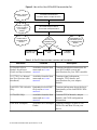
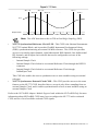
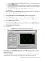
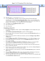
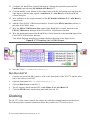
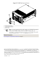
USER MANUAL AND SPECIFICATIONS
NI 5772R
Digitizer Adapter Module
The NI 5772 is a high-speed digitizer adapter module designed to work in conjunction with
your NI FlexRIO™ FPGA module. The NI 5772 features two analog input (AI) channels with
12-bit resolution and sample rates up to 800 MS/s when using both channels or sample rates
up to 1.6 GS/s when using only one channel. The NI 5772R is available in two versions: an
AC-coupled version and a DC-coupled version.
This document contains signal information and lists the specifications of the NI 5772R, which
is composed of the NI FlexRIO FPGA module and the NI 5772. This document also contains
tutorial sections that demonstrate how to acquire data using a LabVIEW FPGA Example VI
and how to create and run your own LabVIEW project with the NI 5772R.
Note NI 5772R refers to the combination of your NI 5772 adapter module and
your NI FlexRIO FPGA module. NI 5772 refers to your NI 5772 adapter module
only.
Note Before configuring your NI 5772R, you must install the appropriate software
and hardware. Refer to the NI FlexRIO FPGA Module Installation Guide and
Specifications for installation instructions.
The following figure shows an example of a properly connected NI FlexRIO device.
Figure 1. NI FlexRIO Device
NI FlexRIO
Adapter Module
+
NI FlexRIO
FPGA Module
=
NI FlexRIO Device
Contents
Electromagnetic Compatibility Guidelines...............................................................................2
Connecting Cables....................................................................................................................3
How to Use Your NI FlexRIO Documentation Set..................................................................3
Front Panel and Connector Pinouts...........................................................................................5
AUX I/O Connector..........................................................................................................7
Block Diagrams.........................................................................................................................8
NI 5772 Component-Level Intellectual Property (CLIP).........................................................9
NI 5772 CLIP..................................................................................................................10
Using Your NI 5772R with a LabVIEW FPGA Example VI.................................................12
FPGA Example VI Steps................................................................................................12
Creating a LabVIEW Project and Running a VI on an FPGA Target............................13
Clocking..................................................................................................................................16
NI 5772 Specifications............................................................................................................18
Analog Input (AI 0 and AI 1)..........................................................................................19
Analog Input Impedance.................................................................................................21
Internal Sample Clock.....................................................................................................27
CLK IN...........................................................................................................................28
REF IN............................................................................................................................28
TRIG (I/O)......................................................................................................................28
AUX I/O (Port 0 DIO <0..3>, Port 1 DIO <0..3>, and PFI <0..3>)...............................29
EEPROM Map................................................................................................................29
Power..............................................................................................................................30
Physical...........................................................................................................................30
Environment....................................................................................................................30
Compliance and Certifications........................................................................................31
Worldwide Support and Services....................................................................................33
Installing PXI EMC Filler Panels...........................................................................................33
Electromagnetic Compatibility Guidelines
This product was tested and complies with the regulatory requirements and limits for
electromagnetic compatibility (EMC) stated in the product specifications. These requirements
and limits are designed to provide reasonable protection against harmful interference when the
product is operated in the intended operational electromagnetic environment.
This product is intended for use in industrial locations. However, harmful interference may
occur in some installations, when the product is connected to a peripheral device or test object,
or if the product is used in residential or commercial areas. To minimize interference with
radio and television reception and prevent unacceptable performance degradation, install and
use this product in strict accordance with the instructions in the product documentation.
Furthermore, any modifications to the product not expressly approved by National Instruments
could void your authority to operate it under your local regulatory rules.
Caution To ensure the specified EMC performance, you must install PXI EMC
Filler Panels (National Instruments part number 778700-01) in adjacent chassis
slots. Installing PXI EMC Filler Panels in all empty slots is recommended. You can
2 | NI 5772R User Manual and Specifications | ni.com
order a kit of six single slot EMC Filler Panels directly from NI by visiting
ni.com/info and entering partnumber.
Caution To ensure the specified EMC performance, operate this product only with
shielded cables and accessories.
Caution To ensure the specified EMC performance, the length of all I/O cables
must be no longer than 3 m (10 ft).
Related Information
Installing PXI EMC Filler Panels on page 33
Connecting Cables
1.
Use any shielded 50 Ω SMA cable to connect signals to the connectors on the front panel
of your device.
2.
Use the SHH19-H19-AUX cable (NI part number: 152629-01 or 152629-02) to connect
to the digital I/O (DIO) and programmable function interface (PFI) signals on the
AUX I/O connector. NI recommends using the SCB-19 connector block to access the
DIO and PFI signals.
How to Use Your NI FlexRIO
Documentation Set
Refer to Figure 2 and Table 1 to learn how to use your FlexRIO documentation set.
NI 5772R User Manual and Specifications | © National Instruments | 3
Figure 2. How to Use Your NI FlexRIO Documentation Set.
INSTALL Hardware
and Software
NI FlexRIO FPGA Module
Installation Guide and Specifications
CONNECT Signals
and Learn About
Your Adapter
Module
NI FlexRIO Adapter Module
User Guide and Specifications
PROGRAM Your
NI FlexRIO System
in LabVIEW FPGA
Module
Are
You New to
LabVIEW FPGA
Module?
LEARN About
LabVIEW FPGA
Module
Yes
No
No
LabVIEW FPGA
Module Help
NI FlexRIO
Help
LabVIEW
Examples
Table 1. NI FlexRIO Documentation Locations and Descriptions
Document
Location
Description
NI FlexRIO FPGA
Available from the Start
Module Installation
menu and at ni.com/
Guide and Specifications manuals.
Contains installation instructions for
your NI FlexRIO system and
specifications for your FPGA module.
NI 5772R User Manual
and Specifications (this
document)
Contains signal information,
examples, CLIP details, and
specifications for your adapter
module.
Available from the Start
menu and at ni.com/
manuals.
LabVIEW FPGA Module Embedded in LabVIEW
Help
Help and at ni.com/
manuals.
Contains information about the basic
functionality of the LabVIEW FPGA
Module.
NI FlexRIO Help
Available from the Start
menu and at ni.com/
manuals.
Contains FPGA Module, adapter
module, and CLIP configuration
information.
LabVIEW Examples
Available in NI Example
Finder.
Contains examples of how to run
FPGA VIs and Host VIs on your
device.
4 | NI 5772R User Manual and Specifications | ni.com
Table 1. NI FlexRIO Documentation Locations and Descriptions (Continued)
Document
Location
Description
IPNet
ni.com/ipnet
Contains LabVIEW FPGA functions
and intellectual property to share.
NI FlexRIO product
page
ni.com/flexrio
Contains product information and
data sheets for NI FlexRIO devices.
Front Panel and Connector Pinouts
Table 2 shows the front panel connector and signal descriptions for the NI 5772.
Caution To avoid permanent damage to the NI 5772, disconnect all signals
connected to the NI 5772 before powering down the module, and connect signals
only after the adapter module has been powered on by the NI FlexRIO FPGA
module.
NI 5772R User Manual and Specifications | © National Instruments | 5
Table 2. NI 5772 Front Panel Connectors
Device Front Panel
NATIONAL
INSTRUMENTS
NI 5772
REF IN
CLK IN
AI 0
Connector
Signal Description
REF IN
External Reference Clock input, 50 Ω, single-ended.
CLK IN
External Sample Clock input, 50 Ω, single-ended.
AI 0
Analog input channel 0, 50 Ω, single-ended.
AI 1
Analog input channel 1, 50 Ω, single-ended.
TRIG
Trigger input and output channel.
AUX I/O
Refer to Table 3 for the signal list and descriptions.
AI 1
TRIG
AUX
I/O
1.6 GS/s
12-Bit
Digitizer
Caution Connections that exceed any of the maximum ratings of any connector on
the NI 5772R can damage the device and the chassis. NI is not liable for any damage
resulting from such connections.
Related Information
NI 5772 Specifications on page 18
6 | NI 5772R User Manual and Specifications | ni.com
AUX I/O Connector
Table 3. NI 5772 AUX I/O Connector Pin Assignments
AUX I/O Connector Pin
18
16
14
12
10
8
6
4
2
Signal
Signal Description
1
DIO Port 0 (0) Bidirectional single-ended (SE) digital I/O (DIO)
data channel.
2
GND
17
3
DIO Port 0 (1) Bidirectional SE DIO data channel.
15
4
DIO Port 0 (2) Bidirectional SE DIO data channel.
5
GND
6
DIO Port 0 (3) Bidirectional SE DIO data channel.
7
DIO Port 1 (0) Bidirectional SE DIO data channel.
8
GND
9
DIO Port 1 (1) Bidirectional SE DIO data channel.
10
DIO Port 1 (2) Bidirectional SE DIO data channel.
11
GND
12
DIO Port 1 (3) Bidirectional SE DIO data channel.
13
PFI 0
Bidirectional SE DIO data channel.
14
NC
No connect.
15
PFI 1
Bidirectional SE DIO data channel.
16
PFI 2
Bidirectional SE DIO data channel.
17
GND
Ground reference for signals.
18
+5 V
+5 V power (10 mA maximum).
19
PFI 3
Bidirectional SE DIO data channel.
19
Ground reference for signals.
13
11
9
7
5
3
1
Ground reference for signals.
Ground reference for signals.
Ground reference for signals.
Caution The AUX I/O connector accepts a standard, third-party HDMI cable, but
the AUX I/O port is not an HDMI interface. Do not connect the AUX I/O port on the
NI 5772 to the HDMI port of another device. NI is not liable for any damage
resulting from such signal connections.
NI 5772R User Manual and Specifications | © National Instruments | 7
Block Diagrams
The following figure shows the NI 5772 block diagram and signal flow.
Figure 3. NI 5772 Connector Signals and NI 5772 CLIP Signal Block Diagram
NI 5772 Adapter Module
LabVIEW FPGA CLIP
REF IN
PLL
HMC 703
Clk Control
PLL Locked
CLK IN
Configuration
Engine
Vconstant
(Free-Running)
800 MHz
VCO
PLL Loop
Filter
ADC Control
Enable PLL
AI 0
AI 1
Analog
In
Path
ADC Data
ADC12D800RF
12
ADC Clock
ADC
Interface
ADC Data
Analog
In
Path
ADC12D800RF
ADC
Interface
12
ADC Clock
Sync Clock
(IoModSyncClk)
User Command
User Command Commit
User Command Idle
User Data
User Command Status
User Return
User Error
PLL Locked
Initialization Done
SPI Device Select
SPI Read
SPI Write
SPI Address
SPI Write Data
SPI Read Data
SPI Idle
AI 0 Data
16 <N..N-3>
AI 0 Data Over Range
<N..N-3>
AI 1 Data
16 <N..N-3>
AI 1 Data Over Range
<N..N-3>
Trigger Input (Sync & Async)
Trigger Output
TRIG
Trigger WE
AD7291
Temperature
Sensor
SClk
Sda
I2C (Shared)
Example
VI*
DIO Port 0 Rd Data <0...3>
DIO Port 0 Wr Data <0...3>
AUX I/O
I2C (Shared)
DIO Port 0 WE Request
DIO Port 0 WE Actual
DIO Port 1 Rd Data <0...3>
DIO Port 1 Wr Data <0...3>
I2C (Shared)
DIO Port 1 WE Request
DIO Port 1 WE Actual
PFI <0...3> Rd Data
PFI <0...3> Wr Data
PFI <0...3> WE
Related Information
Using Your NI 5772R with a LabVIEW FPGA Example VI on page 12
8 | NI 5772R User Manual and Specifications | ni.com
NI 5772 Component-Level Intellectual Property
(CLIP)
The LabVIEW FPGA Module includes component-level intellectual property (CLIP) for HDL
IP integration. NI FlexRIO devices support two types of CLIP: user-defined and socketed.
•
User-defined CLIP allows you to insert HDL IP into an FPGA target, enabling VHDL
code to communicate directly with an FPGA VI.
•
Socketed CLIP provides the same IP integration of the user-defined CLIP, but also allows
the CLIP to communicate directly with circuitry external to the FPGA. Adapter module
socketed CLIP allows your IP to communicate directly with both the FPGA VI and the
external adapter module connector interface.
The following figure shows the relationship between an FPGA VI and the CLIP.
Figure 4. CLIP and FPGA VI Relationship
NI FlexRIO FPGA Module
FPGA
Adapter Module
CLIP Socket
LabVIEW
FPGA VI
User-Defined
CLIP
Socketed
CLIP
Socketed
CLIP
Socketed
CLIP
Fixed I/O
DRAM 1
CLIP Socket
Fixed I/O
DRAM 0
CLIP Socket
DRAM 0
DRAM 1
Fixed I/O
Adapter
Module
External
I/O Connector
User-Defined
CLIP
The NI 5772 ships with socketed CLIP items that add module I/O to the LabVIEW project.
NI 5772R User Manual and Specifications | © National Instruments | 9
NI 5772 CLIP
The NI 5772 ships with the following CLIP items:
•
NI 5772 CLIP—This CLIP provides access to two analog input channels, eight
bidirectional DIO channels, four bidirectional PFI channels, and an input clock selector
that can be configured to use one of the following settings:
– Internal Sample Clock
–
–
–
Internal Sample Clock locked to an external Reference Clock through the REF IN
connector
External Sample Clock through the CLK IN connector
Internal Sample Clock locked to an external Reference Clock through
IoModSyncClock
The CLIP also contains an engine to program the ADC and Sample Clock circuit, either
through predetermined settings for an easier instrument setup, or through a raw SPI
address and data signals for a more advanced setup. In the LabVIEW FPGA Module,
12-bit analog input data is accessed using an I16 data type (left-justified). The DIO
signals are grouped into two ports of four signals each and are accessed using a U8 data
type and a Boolean write enable signal. The four PFI signals are accessed individually
using Boolean indicators.
Although real-time sampling is the default sampling mode on the NI 5772, the NI 5772
CLIP also supports Time-Interleaved Sampling (TIS) on one analog input channel at a
time. TIS enables the device to use both channels on the ADC to sample the same input
channel at different relative phases, which doubles the real-time sampling rate. The
NI 5772 then interleaves the samples to create a waveform as if only one ADC channel
was sampling the waveform at twice the Sample Clock rate. The data is returned on the
AI 0 Data <N..N-3> and AI 1 Data <N..N-3> signals even though the device is only
sampling the single analog input channel that you selected. To configure the NI 5772 for
TIS mode using this CLIP, refer to the NI FlexRIO Adapter Module Support book in the
NI FlexRIO Help.
The following figure demonstrates TIS on an NI 5772 device.
10 | NI 5772R User Manual and Specifications | ni.com
Figure 5. TIS Mode
AI 1 n–3
AI 1 n–2
AI 0 n–3
AI 0 n–2
...
AI 1 n
AI 0 n
AI x
Sample Clock
Note The ADC data sheet refers to TIS as Dual-Edge Sampling (DES).
•
•
NI 5772 Synchronized Reference Clock CLIP—This CLIP is the National Instruments
NI 5772 Terminal Block, and it provides FlexRIO Instrument Development Library
(FIDL) synchronization using an external 10 MHz reference. This CLIP also provides
access to two analog input channels, eight bidirectional DIO channels, four bidirectional
PFI channels, and an input clock selector that can be configured to use one of the
following settings:
Internal Sample Clock
–
–
Internal Sample Clock locked to an external Reference Clock through the REF IN
connector
–
Internal Sample Clock locked to an external Reference Clock though
IoModSyncClock
This CLIP also enables the user to synchronize two or more modules using an external
reference.
NI 5772 Synchronous External Clock CLIP—This CLIP provides access to the same
features as the NI 5772 CLIP, described above, except it only allows sampling from an
external Sample Clock, and it enables synchronization of two or more modules using an
external Sample Clock.
Refer to the NI FlexRIO Adapter Module Support book within the NI FlexRIO Help for more
information about NI FlexRIO CLIP items, how to configure the NI 5772 with a socketed
CLIP, and for a list of available socketed CLIP signals.
NI 5772R User Manual and Specifications | © National Instruments | 11
Using Your NI 5772R with a LabVIEW FPGA
Example VI
Note You must install the software before running this example. Refer to the
NI FlexRIO FPGA Installation Guide and Specifications for more information about
installing your software.
The NI FlexRIO Adapter Module Support software includes an example project to help you
get started creating your LabVIEW FPGA application. This section explains how to use an
existing LabVIEW FPGA example project to generate and acquire samples with the NI 5772R.
This example requires at least one SMA cable for connecting signals to your NI 5772R.
Note The examples available for your device are dependent on the version of the
software and driver you are using. For more information about which software
versions are compatible with your device, visit ni.com/info, enter
rdsoftwareversion in the text field, and click the NI FlexRIO link in the results.
The NI 5772R example project includes the following components:
•
A LabVIEW FPGA VI that you can compile and run on the FPGA embedded in the
hardware
•
At least one VI that runs on Windows and interacts with the LabVIEW FPGA VI
Note In the LabVIEW FPGA Module software, NI FlexRIO adapter modules are
referred to as IO Modules.
Related Information
Block Diagrams on page 8
FPGA Example VI Steps
1.
2.
3.
4.
5.
6.
Connect one end of an SMA cable to AI 0 on the NI 5772 front panel and the other end of
the cable to your device under test (DUT).
Launch LabVIEW.
Click Help»Find Examples to launch the NI Example Finder.
In the NI Example Finder window, select Hardware Input and Output»FlexRIO»IO
Modules»NI 5772.
Select NI 5772 - Getting Started.lvproj.
In the Project Explorer window, open NI 5772 - Getting Started (Host).vi under My
Computer to open the host VI. The Open FPGA VI Reference function in this VI uses
the NI PXI-7952R as the FPGA target by default. If you are using an NI FlexRIO FPGA
module other than the NI PXI-7952R, complete the following steps to change to the
FPGA VI to support your target.
a) Select Window»Show Block Diagram to open the VI block diagram.
b) On the block diagram, right-click the Open FPGA VI Reference (PXI-7952R)
function and select Configure Open FPGA VI Reference.
12 | NI 5772R User Manual and Specifications | ni.com
c)
d)
e)
f)
g)
In the Configure Open FPGA VI Reference dialog box, click the Browse button
next to the Bitfile button.
In the Select Bitfile dialog box that opens, select the bitfile for your desired target.
The bitfile name is based on the adapter module, example type, and FPGA module.
Click the Select button.
Click OK in the Configure Open FPGA VI Reference dialog box.
Save the VI.
7.
On the front panel, in the RIO Resource pull-down menu, select an NI 5772R resource
that corresponds with the target configured in step 6.
8.
Select AI 0 in the AI Channel control.
9.
Set the Trigger Level (V) and the Record Size controls to the desired value.
10. In the Trigger Type box, you can select either Software or Data Edge. If you select
Software, the VI acquires data every time you click the Software Trigger front panel
button. If you select Data Edge, the VI acquires data every time an edge occurs.
11. Click the Run button to run the VI.
12. Click the Software Trigger button if you selected Software in the Trigger Type control.
The VI acquires data and displays the captured waveform on the Acquired Waveform
graph as shown in the figure below.
13. Click the STOP button to stop the VI.
14. Close the VI.
Figure 6. NI 5772 - Getting Started (Host) VI Front Panel
Creating a LabVIEW Project and Running a VI on an
FPGA Target
This section explains how to set up your target and create an FPGA VI and host VI for data
communication. This section focuses on proper project configuration, proper CLIP
NI 5772R User Manual and Specifications | © National Instruments | 13
configuration, and how to access NI 5772 I/O nodes. For more detailed information about
acquiring data on your NI 5772R, refer to the streaming example available in NI Example
Finder.
Creating a Project
1.
Launch LabVIEW, or if LabVIEW is already running, select File»Create Project.
2.
In the Create Project dialog box, select FPGA Template and click OK. The new project
opens in the Project Explorer window.
3.
Save the project as 5772SampleAcq.lvproj.
Creating an FPGA Target VI
1.
In the Project Explorer window, right-click My Computer and select New»Targets
and Devices.
2.
In the Add Targets and Devices on My Computer dialog box, select the Existing
Target or Device option button and expand FPGA Target to display the target.
3.
Select your device and click OK to load the target and target properties into the Project
Explorer window.
4.
In the Project Explorer window, expand FPGA Target (RIOx, PXI-79xxR).
5.
Right-click FPGA Target (RIOx, PXI-79xxR) and select New»FPGA Base Clock.
6.
In the Resource pull-down menu, select IO Module Clock 0 and click OK.
7.
Right-click IO Module in the Project Explorer window and select Properties.
8.
Select theNI 5772 from the IO Module list. The available CLIP for the NI 5772 is
displayed in the General category of the Component Level IP pane. If the information
in the General category is dimmed, select the Enable IO Module checkbox.
9.
Select in the Name list of the Component Level IP pane.
10. In the Clock Selections category, select 200 MHz Clock from the pull-down menu for
Clk200. Leave Clk40 configured as the Top-Level Clock.
11. Click OK.
Note Configuring these clocks is required for proper CLIP operation. Refer to
the NI 5772 CLIP topics in the NI FlexRIO Help for more information about
configuring your clocks.
12. In the Project Explorer window, right-click the FPGA target and select New»VI. A
blank VI opens.
13. Select Windows»Show Block Diagram to open the VI block diagram.
14. In the Project Explorer window, expand the IO Module (NI 5771: NI 5771) tree view.
15. Drag AI 0 Data N–3 to the block diagram.
16. Click the handle on the bottom of the control node with the Positioning tool and drag the
edge down to expose the other signals, AI 0 Data N–2...AI 0 Data N control node.
17. Add a Timed Loop structure around the node.
18. Wire indicators to the output terminals of the IO Module\AI 0 Data N–3...AI 0 Data N.
19. Right-click the input node of the Timed Loop to wire an FPGA Clock Constant. Set this
constant to Divided Sample Clock.
14 | NI 5772R User Manual and Specifications | ni.com
Figure 7. NI 5772SampleAcq (FPGA).vi Block Diagram
20. Save the VI as 5772SampleAcq(Host).vi.
21. Click the Run button. LabVIEW creates a default build specification and begins
compiling the VI. The Generating Intermediate Files window opens and displays the
code generation progress. Next, the Compilation Status window opens and displays the
progress of the compilation. The compilation takes several minutes.
22. Click Close in the Compilation Status window.
23. Save and close the VI.
24. Save the project.
Creating a Host VI
1.
In the Project Explorer window, right-click My Computer and select New»VI to open
a blank VI.
2. Select Window»Show Block Diagram to open the VI block diagram.
3. Place the Open FPGA VI Reference function, located on the FPGA Interface palette, on
the block diagram.
4. Right-click the Open FPGA VI Reference function, and select Configure Open FPGA
VI Reference.
5. In the Configure Open FPGA VI Reference dialog box, select VI in the Open section.
6. In the Select VI dialog box that opens, select 5772SampleAcq (FPGA).vi under your
device and click OK.
7. Click OK in the Configure Open FPGA VI Reference dialog box. The target name
appears under the Open FPGA VI Reference function in the block diagram.
8. Add a While Loop to the block diagram. Place the While Loop to the right of the Open
FPGA VI Reference function.
9. Right-click the conditional terminal inside the While Loop, and select Create Control to
create a STOP button on the VI front panel window.
10. Add the Read/Write Control function, located on the FPGA Interface palette, inside the
While Loop.
11. Wire the FPGA VI Reference Out output of the Open FPGA VI Reference function to
the FPGA VI Reference In input on the Read/Write Control function.
12. Wire the error out output of the Open FPGA VI Reference function to the error in input
of the Read/Write Control function.
NI 5772R User Manual and Specifications | © National Instruments | 15
13. Configure the Read/Write Control function by clicking the terminal section labeled
Unselected, and selecting IO Module/AI 0 Data N–3.
14. Click the handle on the bottom of the control node with the Positioning tool and drag the
edge down to add the other signals, AI 0 Data N–2...AI 0 Data N, to the Read/Write
Control function.
15. Wire indicators to the output terminals of the IO Module\AI 0 Data N–3...AI 0 Data N
control node.
16. Add the Close FPGA VI Reference function, located on the FPGA Interface palette, to
the right of the While Loop.
17. Wire the FPGA VI Reference Out output of the Read/Write Control function to the
FPGA VI Reference In input of the Close FPGA VI Reference function.
18. Wire the error out output of the Read/Write Control function to the error in input of the
Close FPGA VI Reference function.
Your block diagram should now resemble the block diagram in the figure below.
Figure 8. 5772SampleAcq (Host).vi Block Diagram
19. Save the VI as 5772SampleAcq(Host).vi.
Run the Host VI
1.
Connect one end of an SMA cable to AI 0 on the front panel of the NI 5772 and the other
end of the cable to your DUT.
2.
Open the front panel of 5772SampleAcq(Host).vi.
3.
Click the Run button to run the VI.
4.
The VI acquires data from the DUT on AI 0 Data N and AI 0 Data N-1.
5.
Click the STOP button on the front panel and close the VI.
Clocking
The NI 5772 clock source controls the sample rate and other timing functions on the device.
The following table contains information about the possible NI 5772 clock sources.
16 | NI 5772R User Manual and Specifications | ni.com
Table 4. NI 5772 Clock Sources
Clock Source
Frequency1
Description
Internal Free-Running Sample 800 MHz
Clock
The internal Sample Clock is freerunning.
Internal Sample Clock PLL
On (IoModSyncClock)
800 MHz
The internal Sample Clock locks to
IoModSyncClock, which is provided
only though the backplane of
NI PXIe-796x devices.
Internal Sample Clock PLL
On (REF IN)
800 MHz
The internal Sample Clock locks to an
external 10 MHz Reference clock,
which is provided through the REF IN
front panel connector.
External Sample CLock (CLK 400 MHz to
IN)
800 MHz
An external Sample Clock can be
provided through the CLK IN front
panel connector.
Note Do not connect an external Sample Clock with a frequency greater than
800 MHz to the CLK IN front panel connector to acquire data at rates greater than
800 MS/s. Instead, use an external clock with a frequency between 400 MHz and
800 MHz and configure the CLIP to use TIS.
You can configure the NI 5772 to use a variety of sampling modes. By default, the NI 5772
takes samples at 800 MS/s through both analog input channels; however, you can take samples
through one analog input channel to increase the sample rate. The table below lists the
sampling modes available on the NI 5772.
1
You can use TIS to acquire up to 1.6 GS/s. Refer to the NI FlexRIO Help for more information
about configuring your NI 5772 CLIP.
NI 5772R User Manual and Specifications | © National Instruments | 17
Table 5. Sampling Modes
Mode
Sample
Full-Scale
Rate (MS/s)
Input
Power
Range
(dBm)
Number of
Channels
Connection Description
TIS Disabled
(default)
400 to 800
10
2
Use both CH 0 and CH 1. The
device samples both channels
simultaneously.
TIS Enabled,
Multiplexed to
CH 0
800 to 1,600 10
1
Use only CH 0. Disconnect or
terminate unused channels.
TIS Enabled,
Multiplexed to
CH 1
800 to 1,600 10
1
Use only CH 1. Disconnect or
terminate unused channels.
TIS Enabled,
800 to 1,600 16
Non-Multiplexed2
1
Use CH 0 or CH 1. You can
only use one channel. You
must terminate the unused
channel with the 50 Ω
terminator.
NI 5772 Specifications
Specifications are warranted by design and under the following conditions unless otherwise
noted:
Chassis fan speed is set to High. In addition, NI recommends using slot blockers and
•
EMC filler panels in empty module slots to minimize temperature drift.
•
The NI 5772 uses NI LabVIEW and LabVIEW FPGA software.
Specifications describe the warranted product performance over ambient temperature ranges of
0 °C to 55 °C, unless otherwise noted.
Typical values describe useful product performance beyond specifications that are not covered
by warranty and do not include guardbands for measurement uncertainty or drift. Typical
values may not be verified on all units shipped from the factory. Unless otherwise noted,
typical values cover the expected performance of units over ambient temperature ranges of
23 °C ± 5 °C with a 90% confidence level, based on measurements taken during development
or production.
2
This sampling mode is available in the AC-coupled version only.
18 | NI 5772R User Manual and Specifications | ni.com
Nominal values (or supplemental information) describe additional information about the
product that may be useful, including expected performance that is not covered under
Specifications or Typical values. Nominal values are not covered by warranty.
Related Information
Front Panel and Connector Pinouts on page 5
Analog Input (AI 0 and AI 1)
General Characteristics
............................................................................
Number
of channels
Two
Connector type
............................................................................
SMA
Input type
............................................................................
Single-ended, simultaneously sampled or timeinterleaved sampled (TIS)
............................................................................
Input
impedance3
50 Ω, per connector
Input
............................................................................
coupling
AC (-01L version); DC (-02L version)
Digital data resolution
............................................................................
12-bit, signed, binary data4
............................................................................
ADC part number
ADC12D800RF5
............................................................................
Absolute maximum voltage
±10 VDC, +21 dBm (7.1 Vpk-pk)
Typical Specifications
All specifications were tested in TIS Disabled mode unless otherwise specified.
DC offset
AC-coupled
....................................................................±4.3 mV
DC-coupled
....................................................................
±6.5 mV
Full-scale input
............................................................................
+10 dBm (2 Vpk-pk) or +16 dBm (4 Vpk-pk)6
Gain error
....................................................................
AC-coupled
±2.0% full scale range (FSR)
DC-coupled
....................................................................
±6.5% full scale range (FSR)
3
4
5
6
Refer to Figures 8 and 9 for analog input return loss and VSWR.
Data is accessed using an I16 data type (left-justified).
For additional information about the ADC within your device, use the listed part number to locate
the appropriate Texas Instruments data sheet at www.ti.com.
Available in the AC-coupled version and in TIS Enabled, Non-Multiplexed sampling mode only.
NI 5772R User Manual and Specifications | © National Instruments | 19
Table 6. Analog Input Jitter
Integration Range
Internal Free-Running
Internal Locked to IOModSyncCLK
10 Hz to 10 MHz
580 fs rms
770 fs rms
100 Hz to 10 MHz
95 fs rms
175 fs rms
10 kHz to 10 MHz
85 fs rms
85 fs rms
Table 7. Average Noise Density
nV/√Hz
dBm/Hz
dBFS/Hz
AC-coupled
30
-137.5
-147.5
DC-coupled
33
-136.6
-146.6
Table 8. AC Low Cut-Off Frequency (Referenced to Amplitude at 10 MHz)
-3 dB
-1 dB
AC-coupled
110 kHz
240 kHz
DC-coupled
0 kHz
0 kHz
Table 9. Bandwidth And Spectral Performance Summary
Mode
Coupling
Bandwidth
(-3 dB)
Bandwidth
(-1 dB)
SNR
(dB)¹
SFDR
(dBc)¹
THD
(dBc)¹
ENOB
(bits)¹
TIS
Disabled
(default)
ACcoupled
2.27 GHz
780 MHz
58
-65
-63
9.2
DCcoupled
358 MHz
320 MHz
57
-65
-64
9.1
TIS
Enabled,
Muxed to
CH 0
ACcoupled
780 MHz
450 MHz
57
-63
-63
9.0
DCcoupled
356 MHz
312 MHz
57
-63
-65
9.0
TIS
Enabled,
Muxed to
CH 1
ACcoupled
780 MHz
450 MHz
57
-63
-63
9.0
DCcoupled
356 MHz
312 MHz
57
-63
-65
9.0
20 | NI 5772R User Manual and Specifications | ni.com
Table 9. Bandwidth And Spectral Performance Summary (Continued)
Mode
TIS
Enabled,
NonMuxed
Coupling
Bandwidth
(-3 dB)
Bandwidth
(-1 dB)
SNR
(dB)¹
SFDR
(dBc)¹
THD
(dBc)¹
ENOB
(bits)¹
ACcoupled
2.0 GHz
690 MHz
56
-60
-63
8.9
DCcoupled
N/A
N/A
N/A
N/A
N/A
N/A
¹Measured using a -1 dBFS signal at 187 MHz.
Related Information
Analog Input Impedance on page 21
Analog Input Impedance
Analog Input Impedance
Figure 9. Analog Input Return Loss (Multiple Channels Overlaid)
–0
–5
–10
Return Loss (dB)
–15
–20
–25
–30
–35
–40
–45
–50
–55
–60
10 M
400 M
800 M
1.2 G
1.6 G
2G
2.4 G
Input Frequency (Hz)
NI 5772R User Manual and Specifications | © National Instruments | 21
Figure 10. Analog Input VSWR (Multiple Channels Overlaid)
1.8
1.7
1.6
VSWR
1.5
1.4
1.3
1.2
1.1
1.0
0.9
10 M
400 M
800 M
1.2 G
1.6 G
2G
2.4 G
Input Frequency (Hz)
Frequency Response
Note Referenced at 10 MHz using +9 dBm.
Amplitude Response (dB)
Figure 11. AC Low Frequency Response (Referenced to Amplitude at 10 MHz)
1.0
0.0
–1.0
–2.0
–3.0
–4.0
–5.0
–6.0
–7.0
–8.0
–9.0
–10.0
–11.0
–12.0
–13.0
–14.0
–15.0
10 k
1M
100 k
Frequency (Hz)
22 | NI 5772R User Manual and Specifications | ni.com
10 M
Figure 12. High Frequency Response (Referenced to Amplitude at 10 MHz)
0.5
0.0
–1.0
–2.0
Amplitude Response (dB)
–3.0
–4.0
–5.0
–6.0
–7.0
–8.0
–9.0
–10.0
–11.0
AC – TIS Disabled
AC – TIS Enabled Muxed
AC – TIS Enabled Non-Muxed
DC – TIS Disabled
–12.0
–13.0
–14.0
–15.0
10M
100M
1G
3G
Frequency (Hz)
Amplitude Response (dB)
Figure 13. DC Bandwidth (Referenced to Amplitude at 10 MHz)
5
0
–5
–10
–15
–20
–25
–30
–35
–40
–45
–50
–55
–60
–65
–70
–75
–80
–85
–90
–95
–100
DC – Ch0 TIS Disabled
DC – Ch1 TIS Disabled
DC – Ch0 TIS Enabled
DC – Ch1 TIS Enabled
0
200M
400M
600M
800M
1G
1.2G
1.4G
1.6G
Frequency (Hz)
NI 5772R User Manual and Specifications | © National Instruments | 23
Figure 14. DC Bandwidth Flatness (Referenced to Amplitude at 10 MHz)
1.0
1.5
Amplitude Response (dB)
0.0
0.5
–1.0
–1.5
–2.0
–2.5
–3.0
–3.5
DC – Ch0 TIS Disabled
DC – Ch1 TIS Disabled
DC – Ch0 TIS Enabled
DC – Ch1 TIS Enabled
–4.0
–4.5
–5.0
0
40M
80M
120M
160M 200M 240M
Frequency (Hz)
280M
320M
360M
Spectral Measurements
Noise Density (dBm/Hz)
Figure 15. Noise Density
–116
–118
–120
–122
–124
–126
–128
–130
–132
–134
–136
–138
–140
–142
–144
–146
0
80 M
160 M
240 M
Frequency (Hz)
24 | NI 5772R User Manual and Specifications | ni.com
320 M
400 M
400M
Figure 16. One-Tone Spectral Measurement (TIS Disabled, 187 MHz, -1 dBFS)
10
0
–10
Amplitude (dBm)
–20
–30
–40
–50
–60
–70
–80
–90
–100
–110
0
80 M
160 M
240 M
320 M
400 M
Frequency (Hz)
Figure 17. Two-Tone Spectral Measurement (TIS Multiplexed Mode, 182k Samples, 10 Averages)
10
0
–10
Amplitude (dBm)
–20
–30
–40
–50
–60
–70
–80
–90
–100
150 M
160 M
170 M
180 M
190 M
200 M
210 M
220 M
Frequency (Hz)
NI 5772R User Manual and Specifications | © National Instruments | 25
Analog Input Total Phase Noise
Phase Noise (dBc/Hz)
Figure 18. Analog Input Total Phase Noise (353 MHz, -1 dBFS carrier)
–65
–70
–75
–80
–85
–90
–95
–100
–105
–110
–115
–120
–125
–130
–135
–140
–145
–150
Locked to IoModSyncClock
Locked to Front Panel*
Free-Running
10
100
1k
10 k
100 k
1M
10 M
Frequency Offset from Carrier (Hz)
*Uses a 10 MHz Wenzel OCXO (P/N: 501-04609A) as the reference signal.
Crosstalk
Figure 19. AI Crosstalk (Aggressor at -1 dBFS, Victim Terminated to 50 Ω)7
–40
Ch0 Aggressor - Ch1 Victim
Ch1 Aggressor - Ch0 Victim
–45
–50
Cross Talk (dB)
–55
–60
–65
–70
–75
–80
–85
–90
–95
–100
0
300 M 600 M 900 M 1.2 G 1.5 G 1.8 G 2.1 G 2.4 G 2.7 G
Input Frequency (Hz)
7
AC-coupled version only.
26 | NI 5772R User Manual and Specifications | ni.com
3G
Cross Talk (dB)
Figure 20. AI Crosstalk (Aggressor at -1 dBFS, Victim Terminated to 50 Ω)
–40.0
–42.5
–45.0
–47.5
–50.0
–52.5
–55.0
–57.5
–60.0
–62.5
–65.0
–67.5
–70.0
–72.5
–75.0
–77.5
–80.0
–82.5
–85.0
–87.5
–90.0
–92.5
–95.0
–97.5
–100.0
AC – Ch0 Aggressor – Ch1 Victim
AC – Ch1 Aggressor – Ch0 Victim
DC – Ch0 Aggressor – Ch1 Victim
DC – Ch1 Aggressor – Ch0 Victim
0
300M
600M
900M
1.2G
1.5G
1.8G
2.1G
2.4G
2.7G
3G
Input Frequncy (Hz)
Related Information
Typical Specifications on page 19
Internal Sample Clock
General Characteristics
............................................................................
PLL part number
HMC7038
Oscillator type
............................................................................
VCO
Frequency
............................................................................
800 MHz ± 25 ppm
Stability
............................................................................
±5 ppm
Sampling jitter9
............................................................................
90 fs rms
8
9
For additional information about the HMC703, refer to the Hittite data sheet at
www.hittite.com.
Integrated from 100 Hz to 1,600 MHz.
NI 5772R User Manual and Specifications | © National Instruments | 27
CLK IN
General Characteristics
............................................................................
Number of channels
1, single-ended
............................................................................
Connector type
SMA
............................................................................
Frequency range
400 MHz to 800 MHz
............................................................................
Input impedance
50 Ω
............................................................................
Input coupling
AC
............................................................................
Input voltage range
+2 dBm (800 mVpk-pk) to +16 dBm (4 Vpk-pk)
............................................................................
Absolute maximum voltage
±30 VDC, +21 dBm (7.1 Vpk-pk)
............................................................................
Duty cycle
30% to 70%
REF IN
General Characteristics
............................................................................
Number of channels
1, single-ended
............................................................................
Connector type
SMA
............................................................................
Frequency
10 MHz
............................................................................
Input impedance
50 Ω
............................................................................
Input coupling
AC
............................................................................
Input voltage range
+2 dBm (800 mVpk-pk) to 16 dBm (4 Vpk-pk)
............................................................................
Absolute maximum voltage
±30 VDC, +21 dBm (7.1 Vpk-pk)
............................................................................
Duty cycle
30% to 70%
TRIG (I/O)
General Characteristics
............................................................................
Number of channels
1, single-ended
............................................................................
Connector type
SMA
............................................................................
Coupling
DC
28 | NI 5772R User Manual and Specifications | ni.com
Impedance
Input
....................................................................
20 kΩ
Output
....................................................................
50 Ω
Voltage
VIH
....................................................................
2V
V
....................................................................
0.8 V
IL
VOH
....................................................................
2.3 V
VOL
....................................................................
0.7 V
............................................................................
Absolute maximum voltage
±30 VDC, +21 dBm (7.1 Vpk-pk)
AUX I/O (Port 0 DIO <0..3>, Port 1 DIO <0..3>, and
PFI <0..3>)
Number of channels
12 bidirectional (8 DIO and 4 PFI)
............................................................................
Connector type
............................................................................
HDMI
Interface standard
............................................................................
3.3 V LVCMOS
Interface logic
Maximum VIL
....................................................................
0.8 V
Maximum
....................................................................
VIH
2.0 V
Maximum
....................................................................
VOL
0.4 V
....................................................................
Minimum VOH
2.7 V
Maximum
....................................................................
VOH
3.6 V
Z
....................................................................
50 Ω ±20%
out
....................................................................
Iout (DC)
±2 mA
Pull-down
............................................................................
resistor
150 kΩ
Recommended operating voltage
............................................................................
-0.3 V to 3.6 V
Overvoltage protection
............................................................................
±10 V
Maximum toggle frequency
............................................................................
100 MHz
+5 V maximum power
............................................................................
10 mA
+5 V voltage tolerance
............................................................................
4 V to 5 V
EEPROM Map
Caution Only write to User Space. Writing to any other offset may cause the
NI 5772 to stop functioning.
NI 5772R User Manual and Specifications | © National Instruments | 29
Table 10. EEPROM Map
Byte Address
Size (Bytes)
Field Name
0x0
2
Vendor ID
0x2
2
Product ID
0x4
4
Serial Number
0x8
116
Reserved
0x7C
132
User Space
Power
............................................................................
Total
power, typical operation
5.1 W
Physical
............................................................................
Dimensions
12.9 x 2.0 x 12.1 cm (5.1 x 0.8 x 4.7 in.)
............................................................................
Weight
660 g (23.3 oz)
............................................................................
Front panel connectors
5 SMA connectors and one HDMI connector
Clean the hardware with a soft, nonmetallic brush. Make sure that the hardware is completely
dry and free from contaminants before returning it to service.
Environment
............................................................................
Maximum altitude
2,000 m (at 25 °C ambient temperature)
............................................................................
Pollution Degree
2
Indoor use only.
Operating Environment
............................................................................
Ambient temperature range
0 °C to 55 °C (Tested in accordance with
IEC-60068-2-1 and IEC-60068-2-2.)
............................................................................
Relative humidity range
10% to 90%, noncondensing
Note Using the NI 5772 in a
manner not described in this
document may impair the protection
the NI 5772 provides.
(Tested in accordance with IEC-60068-2-56.)
30 | NI 5772R User Manual and Specifications | ni.com
Storage Environment
............................................................................
Ambient temperature range
-40 °C to 70 °C (Tested in accordance
with IEC-60068-2-1 and IEC-60068-2-2.)
............................................................................
Relative humidity range
5% to 95%, noncondensing (Tested in
accordance with IEC-60068-2-56.)
Operational shock
............................................................................
30 g peak, half-sine, 11 ms pulse (Tested in
accordance with IEC-60068-2-27. Test profile
developed in accordance with MILPRF-28800F.)
Random vibration
Operating
....................................................................
5 Hz to 500 Hz, 0.3 grms
Nonoperating
....................................................................
5 Hz to 500 Hz, 2.4 grms (Tested in accordance
with IEC-60068-2-64. Nonoperating test
profile exceeds the requirements of MILPRF-28800F, Class 3.)
Compliance and Certifications
Safety
This product is designed to meet the requirements of the following electrical equipment safety
standards for measurement, control, and laboratory use:
IEC 61010-1, EN 61010-1
•
•
UL 61010-1, CSA 61010-1
Note For UL and other safety certifications, refer to the product label or the Online
Product Certification section.
Electromagnetic Compatibility
This product meets the requirements of the following EMC standards for electrical equipment
for measurement, control, and laboratory use:
•
EN 61326-1 (IEC 61326-1): Class A emissions; Basic immunity
•
•
•
•
EN 55011 (CISPR 11): Group 1, Class A emissions
AS/NZS CISPR 11: Group 1, Class A emissions
FCC 47 CFR Part 15B: Class A emissions
ICES-001: Class A emissions
Note In the United States (per FCC 47 CFR), Class A equipment is intended for
use in commercial, light-industrial, and heavy-industrial locations. In Europe,
NI 5772R User Manual and Specifications | © National Instruments | 31
Canada, Australia, and New Zealand (per CISPR 11), Class A equipment is intended
for use only in heavy-industrial locations.
Note Group 1 equipment (per CISPR 11) is any industrial, scientific, or medical
equipment that does not intentionally generate radio frequency energy for the
treatment of material or inspection/analysis purposes.
Note For EMC declarations, certifications, and additional information, refer to the
Online Product Certification section.
CE Compliance
This product meets the essential requirements of applicable European Directives, as follows:
•
2006/95/EC; Low-Voltage Directive (safety)
2004/108/EC; Electromagnetic Compatibility Directive (EMC)
•
Online Product Certification
To obtain product certifications and the DoC for this product, visit ni.com/certification, search
by model number or product line, and click the appropriate link in the Certification column.
Environmental Management
NI is committed to designing and manufacturing products in an environmentally responsible
manner. NI recognizes that eliminating certain hazardous substances from our products is
beneficial not only to the environment but also to NI customers.
For additional environmental information, refer to the Minimize Our Environmental Impact
web page at ni.com/environment. This page contains the environmental regulations and
directives with which NI complies, as well as other environmental information not included in
this document.
Waste Electrical and Electronic Equipment (WEEE)
EU Customers At the end of the product life cycle, all products must be sent to a
WEEE recycling center. For more information about WEEE recycling centers,
National Instruments WEEE initiatives, and compliance with
WEEE Directive 2002/96/EC on Waste Electrical and Electronic Equipment, visit
ni.com/environment/weee.
电子信息产品污染控制管理办法(中国 RoHS)
中国客户 National Instruments 符合中国电子信息产品中限制使用某些有害物
质指令(RoHS)。关于 National Instruments 中国 RoHS 合规性信息,请登录
ni.com/environment/rohs_china。(For information about China RoHS
compliance, go to ni.com/environment/rohs_china.)
32 | NI 5772R User Manual and Specifications | ni.com
Worldwide Support and Services
The National Instruments website is your complete resource for technical support. At ni.com/
support you have access to everything from troubleshooting and application development selfhelp resources to email and phone assistance from NI Application Engineers.
Visit ni.com/services for NI Factory Installation Services, repairs, extended warranty, and
other services.
Visit ni.com/register to register your National Instruments product. Product registration
facilitates technical support and ensures that you receive important information updates from
NI.
A Declaration of Conformity (DoC) is our claim of compliance with the Council of the
European Communities using the manufacturer’s declaration of conformity. This system
affords the user protection for electromagnetic compatibility (EMC) and product safety. You
can obtain the DoC for your product by visiting ni.com/certification. If your product supports
calibration, you can obtain the calibration certificate for your product at ni.com/calibration.
National Instruments corporate headquarters is located at 11500 North Mopac Expressway,
Austin, Texas, 78759-3504. National Instruments also has offices located around the world.
For telephone support in the United States, create your service request at ni.com/support or
dial 512 795 8248. For telephone support outside the United States, visit the Worldwide
Offices section of ni.com/niglobal to access the branch office websites, which provide up-todate contact information, support phone numbers, email addresses, and current events.
Installing PXI EMC Filler Panels
To ensure specified EMC performance, PXI EMC filler panels must be properly installed in
your NI FlexRIO system. The PXI EMC filler panels (National Instruments part number
778700-01) must be purchased separately. For more installation information, refer to the
NI FlexRIO FPGA Module Installation Guide and Specifications.
1. Remove the captive screw covers.
2.
Install the PXI EMC filler panels by securing the captive mounting screws to the chassis,
as shown in the figure below. Make sure that the EMC gasket is on the right side of the
PXI EMC filler panel.
NI 5772R User Manual and Specifications | © National Instruments | 33
Figure 21. PXI EMC Filler Panels and Chassis
1
2
3
1
1. Captive Screw Covers
2. Captive Mounting Screws
3. EMC Gasket
Note You must populate all slots with a module or a PXI EMC filler panel to
ensure proper module cooling. Do not over tighten screws (2.5 lb · in
maximum). For additional information about the use of PXI EMC filler panels
in your PXI system, visit ni.com/info and enter emcpanels.
Related Information
Electromagnetic Compatibility Guidelines on page 2
Refer to the NI Trademarks and Logo Guidelines at ni.com/trademarks for information on National Instruments trademarks.
Other product and company names mentioned herein are trademarks or trade names of their respective companies. For patents
covering National Instruments products/technology, refer to the appropriate location: Help»Patents in your software, the
patents.txt file on your media, or the National Instruments Patent Notice at ni.com/patents. You can find information about
end-user license agreements (EULAs) and third-party legal notices in the readme file for your NI product. Refer to the Export
Compliance Information at ni.com/legal/export-compliance for the National Instruments global trade compliance policy and
how to obtain relevant HTS codes, ECCNs, and other import/export data.
© 2012—2013 National Instruments. All rights reserved.
373625B-01
Jul13