1
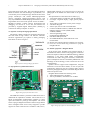
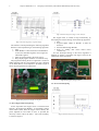
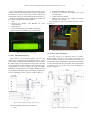
American Journal of Embedded Systems and Applications
2014; 2(2): 6-12
Published online June 30, 2014 (http://www.sciencepublishinggroup.com/j/ajesa)
doi: 10.11648/j.ajesa.20140202.11
Designing an introductory FPGA-based embedded system
laboratory
Swapna Chintakunta, Raghavendra Rao Kanchi, Ramanjappa Thogata
VLSI and Embedded System Laboratory, Department of Physics, Sri Krishnadevaraya University, ANANTAPURAMU, 515003, India
Email address:
[email protected] (R. R. Kanchi)
To cite this article:
Swapna Chintakunta, Raghavendra Rao Kanchi, Ramanjappa Thogata. Designing an Introductory FPGA-Based Embedded System
Laboratory. American Journal of Embedded Systems and Applications. Vol. 2, No. 2, 2014, pp. 6-12. doi: 10.11648/j.ajesa.20140202.11
Abstract: In this paper, we present a series of experiments useful in designing an Embedded System Laboratory. The
experiments are built around the Spartan3 XC3S400 manufactured by Xilinx. The necessary code is written in the Very High
Speed Integrated Circuit Hardware Description Language (VHDL). Integrated Simulation Environment (ISE) Version 9.1i
suite is used for software development which is one of the Electronic Design Automation (EDA) tool offered by the Xilinx
Company. It gives a good beginning for students who want to work on Spartan 3 XC3S400.
Keywords: FPGA, Spartan 3, VHDL, Embedded System Laboratory
1. Introduction
The impact and presence of embedded system is felt
directly in our daily walk of life. Starting with cellular phones,
digital cameras, home appliances, space applications up to
ubiquitous networking and sensor networking embedded
system are used [1]. Traditionally, the designers have three
options to realize device hardware control platform. These are
Digital Signal Processors (DSPs), Field Programmable Gate
Arrays (FPGAs) and Application Specific Integrated Circuits
(ASICs). Digital Signal Processors execute only one
operation at a time, so the overall algorithm proceeds in a
sequential manner. For cost reduction purposes, ASICs are
introduced in high volume production series. However, a lot
of effort and costs are related with production of specific
ASIC, which makes this technology unsuitable for Research
and Development (R&D) stage of a new product. Between
these two extremes, FPGAs provide a compromise between
DSPs and ASICs, combining many advantages of both. This
makes FPGAs suitable in several applications.
FPGA-based devices are especially well suited for
building application – specific systems as a starting point in
an undergraduate embedded system design course. FPGAbased design have a much shorter design cycle, lower cost
and a smoother learning curve than the traditional
system-on-chip technology [2]. When it comes to laboratory,
the kind of exposure and training the student gets is meager.
In certain cases demo experiments were introduced. This
hinders the practical training the student is expected to get in
the embedded system training laboratory.
Keeping these facts in view point, we have designed and
developed certain experiments using the Spartan XC3S400
manufactured by Xilinx [3]. These experiments are
presented in this paper. It Starts with LED BLINKY
experiment and goes up to the sensor interfacing.
2. Description to FPGA and Spartan 3
2.1. Field Programmable Gate Array (FPGA)
A field-programmable gate array (FPGA) is an integrated
circuit designed to be configured by a customer or a designer
after manufacturing in the field and hence called
“field-programmable". Field Programmable Gate Array
(FPGA) is a general-purpose, multi-level programmable
logic device that is customized in the package by the end
users. FPGAs are composed of blocks of logic connected
with programmable interconnect. The programmable
interconnect between blocks allows users to implement
multi-level logic, removing many of the size limitations of
the Programmable Logic Devices (PLD)-derived two-level
logic structure. This extensible architecture can currently
support thousands of gates of logical system and speeds in
the tens of megahertz.
The size, structure and number of blocks; and the amount
and connectivity of interconnect vary considerably among
FPGA architectures. This difference in architectures is
driven by different programming technologies and different
7
Swapna Chintakunta et al.:
Designing an Introductory FPGA-Based Embedded System Laboratory
target applications of the parts. The system design based on
FPGA is flexible with the advantages of parallelism, low
cost and low power consumption [4]. FPGAs fall into three
groups: Island-style and cellular SRAM-programmed
devices; channeled, antifuse-programmed devices; and
array-style EPROM or EEPROM-programmed devices. The
target FPGA device used in the present work is XC3S400 –
SPQ208 of Spartan 3 family. Design, development and
debugging are carried on a low cost, full featured kit
provided by Applied Digital Microsystems (ADM) [5],
connected to desktop computer via JTAG.
2.2. Spartan 3 Family Packaging Information
The Spartan 3 family of FPGA is specifically designed to
meet the needs of high volume, cost effective consumer
electronic applications [6]. Spartan 3 family packaging
information is shown in figure 1.
TQFP, PQFP packages up to 240 pins. Figure 2 shows the
photograph of the FPGA base board used in the present
work.
The Specifications of base board are as follows [7]
1. 16x2 Alpha-numeric LCD display with the backlight
2. Four digit 7-segment display , Eight general purpose
LEDS
3. Three LEDs to indicate the various power voltages
4. 4x4 Matrix Keypad
5. 208 I/O pins, All I/O with VCC/GND links
6. On board 10 MHz oscillators, 10MHz clock and four
different frequency clocks (5MHz,1MHz,
500KHz,100KHz)
7. JTAG Programming Cable,
Parallel/Serial/USB/SPI/CAN
8. PS2 Mouse &Keyboard I/F
9. I2C EEPROM & RTC, Serial ADC/DAC with
Potentiometer
10. RS232 serial interface through 9-PIN D type connector
11. Four sets of 30x2 male berg connectors to plug the
Daughter Board
2.4. Details of Spartan 3 Daughter Board
Fig. 1. Spartan 3 Family packaging information
2.3. Specifications of FPGA Base Board
In the present work, daughter board contains Spartan 3
XC3S400 from Xilinx, which can be plugged on to the base
board. The Spartan 3 FPGA uses SRAM technology. SRAM
Technology is the Static RAM FPGA. Programmable
connections are made using pass transistors, transmission
gates or multiplexers that are controlled by SRAM cells. The
advantage of this technology is that it allows fast in-circuit
reconfiguration.
Spartan-3 devices support serial configurations, using the
master/slave serial and JTAG modes, as well as byte-wide
configuration employing the slave parallel mode. Figure3
shows the photograph of Spartan 3 XC3S400 daughter board
used in the present work.
Daughter Board includes the following items
1. Xilinx FPGA Spartan 3 XC3S400
2. Ten 10-pin Headers, intended for use as GPIO
Fig. 2. Photograph of the FPGA base board
The ADM base board is a powerful tool that allows user to
understand the capabilities of FPGA. This board acts as a
FPGA reconfigurable implementation platform to allow
rapid and interactive prototype development. The board
houses a plug-in daughter board that contains a target FPGA
device. Daughter board can be easily swapped to provide
support for multi-vendor devices available in DIL, PLCC,
Fig. 3. Photograph of Spartan 3 XC3S400 daughter board
American Journal of Embedded Systems and Applications 2014; 2(2): 6-12
8
3. Details of JTAG Connector
FPGAs can be configured by using different modes like
Boundary Scan, Slave Serial, or Select MAP. The most
commonly used mode is Boundary Scan, Also known as
JTAG (Joint Test Action Group). The boundary Scan
Register and other test features of the device are accessed
through a standard interface – the JTAG Test Access Port
(TAP). According to this standard, the TAP must contain
four signals, TDI (Test Data Input), TDO (Test Data output),
TCK (Test Clock), TMS (Test Mode Select) [8]. Parallel
download cable is connected to the board through the JTAG
port at one end and other end of the cable is connected to PC
parallel port.
Xilinx FPGAs are SRAM – based and must be
programmed every time power is cycled. The most common
method of programming Xilinx FPGAs is by using Xilinx
PROM connected to a chain of FPGA as shown in figure 4.
These PROMS must be programmed using PROM files
created from the FPGA chain bit streams. PROM files
include information on the FPGA chain length and contain
bit streams that are reformatted for use with PROM file
formats available: .mcs,. exo, .rek,. hex, .ufp, and. bin. In
the present work FPGA is programmed using bit file and
PROM is Programmed using .mcs file. Figure 4 shows the
JTAG chain configured devices.
Fig. 5. Schematic diagram of LED Blink Shift
The software is developed basing on the following
algorithm.
1. Start.
2. Make Header1 as data out direction.
3. Initialize the header1 with 0x01.
4. Realization of led blink shift by making Header1
logical left shift with ‘1’.This program is kept in
continuous loop.
Program describing the above algorithm is written in
VHDL language, and the corresponding .mcs file is dumped
on the flash memory of the Spartan 3 XC3S400. The
photograph of the hardware is shown in figure 6. The blank
shift is observed at the bottom of the board.
Fig. 4. JTAG Chain the Configured devices
4. Details of Individual Experiments
In this paper, the features of Spartan 3 XC3S400 are used
and well explained by the following experiments. These
experiments are useful for FPGA beginners. VHDL
language is used for programming FPGA. The software
tools used for building and testing the experiments in the
present work is Xilinx ISE 9.1 i [9].
Fig. 6. Photograph of LED blink shift
4.1. Ex.1.LED Blink Shift
4.2. Ex.2.Multiplexed Seven Segment Display Interfacing
In this experiment, Header 1 is used as output port. The
circuit assembly is shown in figure 5.
In this experiment Header1 is used for interfacing
multiplexed seven segment display and header2 is used to
drive the individual segment control signal for individual
character. Figure 7 shows the circuit assembly.
9
Swapna Chintakunta et al.:
Designing an Introductory FPGA-Based Embedded System Laboratory
Fig. 9. Schematic diagram of Stepper motor Interface
Fig. 7. Schematic diagram of 7-Segment display
The software is developed basing the following algorithm
Software is developed basing on the following algorithm.
1. Start
2. Make Header1 as data out direction and Header2
as drive the individual segment control signal for
individual segment.
3. Enter the look-up table in the form of array.
4. Keep displaying hex numbers in continuous loop.
The program describing the above algorithm is written in
VHDL language and the corresponding .mcs file is dumped
on the flash memory of the Spartan 3 XC3S400. Figure 8
shows the photograph of the experiment.
The stepper motor is rotated in steps continuously, by
developing the software basing on the following algorithm.
1. Start.
2. Program higher nibble of Header1 as data out
direction.
3. Send the data through Header1.
4. Keep on sending data which rotates motor
continuously.
.mcs file developed basing on the above algorithm is
dumped on Spartan 3 XC3S400. The figure 10 shows the
photograph of the experiment.
Fig. 10. Photograph of Stepper Motor
4.4. Ex.4. LCD Interfacing
Fig. 8. Photograph of 0-F display on 7-Segment
4.3. Ex.3.Stepper Motor Interfacing
In this experiment the stepper motor is interfaced with
Spartan 3 XC3S400 using Header1. As the Header1 output
of the FPGA cannot drive the stepper motor directly, the
power amplifier IC ULN 2003 is used. It provides the
necessary current to drive the motor. The circuit assembly
is shown in figure 9.
Fig. 11. Schematic diagram of LCD interfacing
American Journal of Embedded Systems and Applications 2014; 2(2): 6-12
A 16x2 LCD module [10] is used in this experiment; LCD
module is used in 8 bit mode. Header1 used for sending data
and Header2 is used as control pins, between FPGA and
LCD module. The circuit is assembled as shown in figure11.
Program is developed to display ADM on first and second
lines of LCD using the following algorithm:
1. Start
2. Initialize the Header1 and Header2 for LCD
communication
3. Initialize LCD
4. Keep on sending characters ADM continuously.
Figure 12 shows the ADM display on LCD module.
10
2.
3.
Initialize the Header1 as output port
Initialize the Header2 and Header3 for LCD
communication
4. Output data from Header1.
5. Measure the external input voltage and display
decimal value on LCD.
The photograph of ADC value display on LCD is shown
in figure 14.
Fig. 14. Photograph of ADC value display on LCD
Fig. 12. Photograph of LCD Interfacing
4.5. Ex.5. ADC 0804 Interfacing
ADC 0804 is an 8-bit analog-to-digital converter [11]
which works on successive approximation principle. In the
present setup a 10kΩ/10 turn potentiometer is connected to
the analog input of ADC 0804. The voltage span is selected
as 0 to 5V. Program is developed to display the digital value
corresponding to analog voltage (as read by digital
multimeter) is displayed on LCD module. Headers 1 and 2
are programmed as output ports and header 3 as input port.
The corresponding circuit is shown is shown in figure 13.
4.6. Ex.6. DC Motor Interfacing
DC motor control is an important aspect in industry.
Keeping this in view point, a DC motor is interfaced via a
power amplifier ICL293 [12]. The direction of rotation is
determined by the IC MOC70P2 [13]. Software is developed
to control the rotational direction of DC motor and the speed
of rotation using opto-sensor. The circuit assembled as
shown in figure 15.
Fig. 13. Schematic diagram of ADC 0804 interfacing
The corresponding algorithm is given below.
1. Start.
Fig. 15. Schematic diagram of DC motor interfacing
11
Swapna Chintakunta et al.:
Designing an Introductory FPGA-Based Embedded System Laboratory
The corresponding algorithm is given below:
1. Start
2. Initialize the Header1 as output port
3. Initialize the Header 2 as input port
4. Measure speed and direction of dc motor and
display continuously.
The photograph of the DC Motor interfacing experiment
is shown in figure 16.
Fig. 18. Photograph of Heart beat measurement system
5. Conclusion
Fig. 16. Photograph of DC motor interfacing
4.7. Ex.7. Heart Beat Measurement System
As a project-based experiment, we have designed and
developed a heart beat measuring circuit. The FPGA based is
interfaced with the heart beat sensor system [14]. The basic
principle that underlies the measurement is the pulsating
blood flow through artery of the finger tip. The schematic
circuit diagram of heart beat measurement system is shown
in figure 17.
A series of experiments useful for Under-graduate
ECE/CSE laboratory designed and developed in author’s
laboratory is explained in this paper. These experiments can
be introduced in a laboratory course. The hands on
experience a student get by performing these experiments
definitely give a confidence to think and develop a complex
FPGA-based interfacing which is very much need in the
present scenario of hardware revolution.
Acknowledgement
C. Swapna is thankful to University Grants Commission
(U.G.C.), New Delhi, for the sanction of Junior Research
Fellowship (B.S.R.).
References
[1]
Aruna Kommu, Raghavendra Rao Kanchi, “Design and
development of a project-based embedded system laboratory
using LPC1768”, American Journal of Embedded Systems
and Applications, Vol.1, No.2, November 2013. pp 46-53.
[2]
John Bowles and Gang Quan, “An FPGA – Based Embedded
System Design Laboratory for the Undergraduate Computer
Engineering Curriculum”, American society for Engineering
Education, AC2009-761.
[3]
www.xilinx.com/spartan3LC.pdf.
[4]
Jayaram Bhaskar (1998): A “VHDL Primer”, 3 rd Edition,
PTR Prentice Hall.
[5]
Applied Digital Microsystems (ADM) Pt, Ltd., Mumbai.
[6]
Spartan – 3FPGA family: Complete datasheet DS099, 2009.
http://www.Xilinx.com/support/documentation/data
sheets/ds321.pdf.
[7]
ADM TKB 208 user Manual – XC3SXX D-board, Applied
Digital Microsystems, Mumbai, http://www.admlindia.com.
[8]
JTAG
Interface:
simple
www.amontec.com/amt-ann004.pdf.
[9]
ISE
9.1i
Quick
Start
Tutorial.
http://www.xilinx.com/itp/Xilinx/books/docs/qst/ast.pdf.
Fig. 17. Schematic diagram of Heart beat measurement system
Program for Heart Beat Measurement System is
developed using below Algorithm:
1. Start
2. Initialize the pulse counter
3. Initialize the LCD communication
4. Display Heart Beat Pulses per minute on LCD
5. Display the heart beat pulses in the form of LED
The photograph of heartbeat measurement system is
shown in figure 18.
introduction,
[10] http://pdf/.alldatasheet.com/datasheet-pdf/view/111499/HIT
ACHI/HD447
American Journal of Embedded Systems and Applications 2014; 2(2): 6-12
[11] www.ti.com/lit/ds/symlink/adc0804-n.pdf
[12] www.ti.com/lit/ds/symlink/l293d.pdf
[13] http://datasheet.octopart.com/MOC70P2-Fairchild-datasheet
-8378515.pdf
12
[14] Swapna. C, Vijay Kumar. J, Raghavendra Rao. K,
Ramanjappa.T,“FPGA Based Heart Beat Measurement
System”, International Conference on Information
Technology, Electronics and communications (ICITEC),
July 14 – 15, 2012, Hyderabad, India.