1
User Manual
VX4801
Programmable Digital I/O Module
070-9153-03
This document applies for firmware version 1.00
and above.
Copyright Tektronix, Inc. All rights reserved.
Tektronix products are covered by U.S. and foreign patents, issued and pending. Information in this publication supercedes
that in all previously published material. Specifications and price change privileges reserved.
Printed in the U.S.A.
Tektronix, Inc., P.O. Box 1000, Wilsonville, OR 97070–1000
TEKTRONIX and TEK are registered trademarks of Tektronix, Inc.
WARRANTY
Tektronix warrants that this product will be free from defects in materials and workmanship for a period of three
(3) years from the date of shipment. If any such product proves defective during this warranty period, Tektronix,
at its option, either will repair the defective product without charge for parts and labor, or will provide a
replacement in exchange for the defective product.
In order to obtain service under this warranty, Customer must notify Tektronix of the defect before the expiration
of the warranty period and make suitable arrangements for the performance of service. Customer shall be
responsible for packaging and shipping the defective product to the service center designated by Tektronix, with
shipping charges prepaid. Tektronix shall pay for the return of the product to Customer if the shipment is to a
location within the country in which the Tektronix service center is located. Customer shall be responsible for
paying all shipping charges, duties, taxes, and any other charges for products returned to any other locations.
This warranty shall not apply to any defect, failure or damage caused by improper use or improper or inadequate
maintenance and care. Tektronix shall not be obligated to furnish service under this warranty a) to repair damage
resulting from attempts by personnel other than Tektronix representatives to install, repair or service the product;
b) to repair damage resulting from improper use or connection to incompatible equipment; or c) to service a
product that has been modified or integrated with other products when the effect of such modification or
integration increases the time or difficulty of servicing the product.
THIS WARRANTY IS GIVEN BY TEKTRONIX WITH RESPECT TO THIS PRODUCT IN LIEU OF
ANY OTHER WARRANTIES, EXPRESSED OR IMPLIED. TEKTRONIX AND ITS VENDORS
DISCLAIM ANY IMPLIED WARRANTIES OF MERCHANTABILITY OR FITNESS FOR A
PARTICULAR PURPOSE. TEKTRONIX’ RESPONSIBILITY TO REPAIR OR REPLACE DEFECTIVE
PRODUCTS IS THE SOLE AND EXCLUSIVE REMEDY PROVIDED TO THE CUSTOMER FOR
BREACH OF THIS WARRANTY. TEKTRONIX AND ITS VENDORS WILL NOT BE LIABLE FOR ANY
INDIRECT, SPECIAL, INCIDENTAL, OR CONSEQUENTIAL DAMAGES IRRESPECTIVE OF
WHETHER TEKTRONIX OR THE VENDOR HAS ADVANCE NOTICE OF THE POSSIBILITY OF
SUCH DAMAGES.
EC Declaration of Conformity
We
Tektronix Holland N.V.
Marktweg 73A
8444 AB Heerenveen
The Netherlands
declare under sole responsibility that the
VX4801
meets the intent of Directive 89/336/EEC for Electromagnetic Compatibility.
Compliance was demonstrated to the following specifications as listed in the Official
Journal of the European Communities:
EN 55011
Class A Radiated and Conducted Emissions
EN 50081-1 Emissions:
EN 60555-2
AC Power Line Harmonic Emissions
EN 50082-1 Immunity:
IEC 801-2
Electrostatic Discharge Immunity
IEC 801-3
RF Electromagnetic Field Immunity
IEC 801-4
Electrical Fast Transient/Burst Immunity
IEC 801-5
Power Line Surge Immunity
To ensure compliance with EMC requirements this module must be installed in a
mainframe which has backplane shields installed which comply with Rule B.7.45 of
the VXIbus Specification. Only high quality shielded cables having a reliable,
continuous outer shield (braid & foil) which has low impedance connections to
shielded connector housings at both ends should be connected to this product.
$$#
$ " "$ !$ #
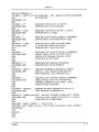
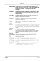
0641'7&6,10 10641.5 0' 0',&$6145 9,6&+(5 75(5 5 7,.6=0 (56 37,2/(06 .155$4; 2(&,),&$6,105 $ "!"$ " #
056$..$6,10 (37,4(/(065 0' $76,105 056$..$6,10 41&('74( 056$..$6,10 +(&-.,56 $ !"$ 8(48,(9 19(4=72 ;56(/ 1//$0'5 1'7.( 2(4$6,10 1//$0' ;06$: 1//$0' 7//$4; 1//$0' (5&4,26,105 # (.) (56 $0' 0,6,$.,<$6,10 $ " " %!#
(),0,6,10 1) 1//$0'5 41*4$//,0* :$/2.( 0 !!#
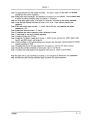
22(0',: !"%75 2(4$6,10 22(0',: 027676276 100(&6,105 22(0',: !" .155$4; 22(0',: 5(4 (48,&( 22(0',: (4)14/$0&( !(4,),&$6,10 General Safety Summary
Review the following safety precautions to avoid injury and prevent damage to
this product or any products connected to it.
Only qualified personnel should perform service procedures.
While using this product, you may need to access other parts of the system. Read
the General Safety Summary in other system manuals for warnings and cautions
related to operating the system.
Injury Precautions
Avoid Electric Overload
To avoid electric shock or fire hazard, do not apply a voltage to a terminal that is
outside the range specified for that terminal.
Do Not Operate Without
Covers
To avoid electric shock or fire hazard, do not operate this product with covers or
panels removed.
Use Proper Fuse
To avoid fire hazard, use only the fuse type and rating specified for this product.
Do Not Operate in
Wet/Damp Conditions
Do Not Operate in an
Explosive Atmosphere
To avoid electric shock, do not operate this product in wet or damp conditions.
To avoid injury or fire hazard, do not operate this product in an explosive
atmosphere.
Product Damage Precautions
Provide Proper Ventilation
Do Not Operate With
Suspected Failures
To prevent product overheating, provide proper ventilation.
If you suspect there is damage to this product, have it inspected by qualified
service personnel.
VX4801 Programmable Digital I/O Module
iii
General Safety Summary
Safety Terms and Symbols
Terms in This Manual
These terms may appear in this manual:
WARNING. Warning statements identify conditions or practices that could result
in injury or loss of life.
CAUTION. Caution statements identify conditions or practices that could result in
damage to this product or other property.
Terms on the Product
These terms may appear on the product:
DANGER indicates an injury hazard immediately accessible as you read the
marking.
WARNING indicates an injury hazard not immediately accessible as you read the
marking.
CAUTION indicates a hazard to property including the product.
Symbols on the Product
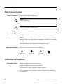
The following symbols may appear on the product:
DANGER
High Voltage
Protective Ground
(Earth) Terminal
ATTENTION
Refer to Manual
Double
Insulated
Certifications and Compliances
Overvoltage Category
Overvoltage categories are defined as follows:
CAT III: Distribution level mains, fixed installation
CAT II: Local level mains, appliances, portable equipment
CAT I: Signal level, special equipment or parts of equipment, telecommunication, electronics
iv
VX4801 Programmable Digital I/O Module
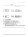
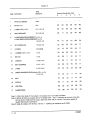
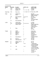
Output high voltage (Voh)
Io = –20 A
lo = –6 mA
Output low voltage (Vol)
lo = 20 A
lo = 24 mA
Output low current (lol)
Input high voltage (Vih)
Input low voltage (Vil)
* Input current (lin)
Tri-state leakage current (loz)
min
typ
4.4
3.84
5.0
4.2
0
0
max
V
V
0.1
0.5
24
2.0
0.5
units
0.8
230
5.0
* There are 22 k pull-up resistors to + 5V on all I/O and handshake lines to account for floating inputs.
The inputs IC use 1.0 A max, while the pull-down resistors require 5V / 22 k = 227.6 A.
–10 ° to +55 ° C., typical specs at 25° C. A minus sign indicates current flowing out of the card.
V
V
mA
V
V
A
A
Appendix E: Performance Verification123
This procedure verifies the performance of the VX4801 Programmable Digital
I/O Module. The test sequences may be performed in your current VXIbus
system if it meets the requirements described in Table 2. Also, it is not necessary
to complete the entire procedure if you are only interested in a specific performance area. Some tests depend on the proper operation of previously verified
functions so it is best to follow the order as presented.
The following skills are required to perform this procedure:
H
Thorough knowledge of test instrument operation and proper measurement
techniques
H
Knowledge of VXIbus system components and command language
programming
H
Ability and facility to construct interconnections and fixtures as needed to
perform the procedure
General Information and Conventions
Please familiarize yourself with the following conventions which apply
throughout this procedure:
H
Each test sequence begins with a table, similar to the one below, which
provides information and requirements specific to that section. The item
number appearing after each piece of equipment refers to an entry in Table 1
Required Test Equipment. Immediately following the table, you will be given
instructions for interconnecting the VX4801 under-test and for checking the
performance parameters. Results may then be recorded on a photocopy of the
Test Record on page A–23.
Equipment
Requirements
Digital Volt Meter (item 1)
Loop-Back Cable Assembly (item 3)
Prerequisites
All prerequisites listed on page A–20
H
This procedure assume that you will be using the National Instruments PC
GPIB controller and software (NI-488.2M) configured as described in
Table 3. In the test sequences, you will be instructed to issue Interface Bus
Interactive Control (ibic) commands to set up the VX4801 under-test and
other associated VXIbus test instruments. Please refer to the NI-488.2M
User Manual for additional information. If you are using a different
controller or software, simply substitute the equivalent commands.
VX4801 Programmable Digital I/O Module
A–19
Appendix E: Performance Verification
NOTE. Commands to the VX4801 may be entered in upper or lower case.
However, to avoid confusion between the alphanumeric characters; e.g. one (1)
and L or zero( 0) and o, all commands are shown in the case which provides the
greatest distinction. Use special care when interpreting these characters.
Prerequisites
The verification sequences in this procedure are valid when the following
requirements are met:
H
The VX4801 module covers are in place and the module is installed in an
approved VXIbus mainframe as described in Section 2 of the Operating
Manual
H
The VX4801 has passed the power-on self test
H
The VX4801 is operating in an ambient environment as specified in
Section 1 of the Operating Manual for a warm–up period of at least 10
minutes
Equipment Required
This Procedure uses traceable signal sources and measurement instruments.
Table 1 lists the required equipment. You may use equipment other than the
recommended examples if it meets the minimum requirements.
Table 1: Required Test Equipment
Item Number and Description
Minimum Requirements
Example
Purpose
1.
Digital Volt Meter (DVM)
5-1/2 digit, 100 VDC range, accuracy
> 0.002 %.
FLUKE 8842A
Checking isolation impedance
2.
Digital I/O Module
4 byte TTL/CMOS data I/O
Tektronix VX4801
Checking external functions
3.
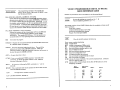
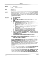
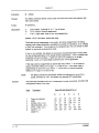
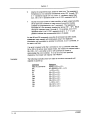
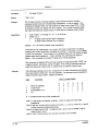
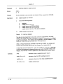
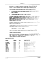
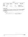
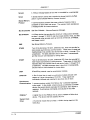
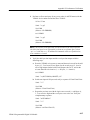
Loop-Back Cable Assembly
Male DB-50 Connector, two required
(Tektronix part number 131-1344-00)
Assemble as shown in
Figure 4
Checking TTL/CMOS Data
I/O, Tri-State, and Handshake.
Male DB-25 Connectors, are required
(Tektronix part number 131-0570-00)
26 AWG ribbon wire
A–20
VX4801 Programmable Digital I/O Module
Appendix E: Performance Verification
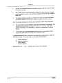
DB-25 Male
25
13
Byte 5 Tri-St
Byte 4 Tri–St
Byte 5 LSB
14
Byte 4 LSB
1
8
DB-50 Male
DB-50 Male
Byte 2
50
33
17
Byte 3 LSB
Byte 2 MSB
Byte 3 Tri-St
Byte 0 Tri-St
GND
Byte 3
33
50
17
Byte 0 LSB
6
5
39
DAK
DAV
Byte 1
GND
GND
GND
34
18
1
34 18 1
DRd
RFD
Allow approximately 6”
length of interconnect
wire between modules.
Byte 1 Tri-St
Byte 2 Tri-St
VX4801 Under-test
VX4801 Slave Module
Figure 4: Loop-Back Cable Assembly (View of Solder Side)
VX4801 Programmable Digital I/O Module
A–21
Appendix E: Performance Verification
VX4801 Under-Test Configuration
In order to perform this procedure, the VX4801 under-test must be installed in an
approved VXIbus system. At a minimum, the system must contain the elements
listed in Table 2.
Table 2: Elements of a Minimum VX4801 Under-Test System
Item Number and Description
Minimum Requirements
Example
Purpose
1.
VXIbus Mainframe
Two available slot for VX4801
under-test and the VX4801 digital
signal source (Slave) in addition to
the Slot 0 controller
Tektronix VX1400A
Provides power, cooling, and
backplane for VXIbus modules
2.
Slot 0 Controller
Resource Mgr., Slot 0 Functions,
IEEE 488 GPIB Interface
VX4521 Slot 0 Resource Mgr.
Provides Slot 0 functions.,
Resource Mgr., and GPIB/
VXIbus interface
3.
VXIbus System Controller
VXIbus-Talker/Listener/Controller
IBM 486 PC with National
Instruments GPIB PC2A card
& NI-488.2M software, GPIB
cable (Tektronix P/N
012–0991-00)
Provides VXIbus command
and response interface
4.
VX4801 Under-Test
Not applicable
Not applicable
Verify its performance
5.
VX4801-Slave
4 byte TTL/CMOS I/O
VX4801
Provides test signal I/O
Test System Configuration
Table 3 describes the VXIbus system configuration assumed in this procedure. If
your configuration is different, you do not need to change it, just note that you
will observe your device names and addresses in test sequences. (Note that no
secondary addressing is assumed.)
Table 3: Test System Configuration (Assumed)
A–22
Device
GPIB Device
Name
VXI Slot
VXIbus Logical
Address
GPIB Primary
Address
GPIB0
GPIB0
(PC card)
NA
30
VX4521
VX4521
Slot 0
0D (hex)
13
VX4801 under-test
VX4801
Slot 1
01
1
VX4801 slave
slave
Slot 2
02
2
VX4801 Programmable Digital I/O Module
Appendix E: Performance Verification
Test Record
Photocopy the Test Record, and use it to record the performance verification
results for your module.
Table 4: VX4801 Test Record
VX4801 Serial Number:
Temperature and Relative Humidity:
Date of Last Calibration:
Verification Performed by:
Certificate Number:
Date of Verification:
Table 5: VX4801 Performance Tests
VXIbus Interface Checks
Table Command Response
Logical Address, IEEE Address, Slot No., MFG., Model, etc.
1st. Response
2nd Response
3rd Response
Passed
Preliminary Tests
Failed
Self Test
Interrupt SRQ
TTL/CMOS I/O Data Bytes
Tri-State Control Signals
Internal
External
Handshake Control Signals
Transmit
Receive
VX4801 Programmable Digital I/O Module
A–23
Appendix E: Performance Verification
Self Test
The VX4801 includes a built-in self test function (BITE) which is automatically
executed each time the power is turned on and when the Internal Self Test (S)
command is issued. BITE uses internal routines and circuitry to confirm basic
I/O functionality. No external test equipment is required.
During self test, all outputs are set to a high impedance (tri-state) mode and then
internal loop-back circuitry and test patterns are used to verify all I/O channels.
In addition to BITE, front panel indicator lights display the current status of
power, the assertion of SYSFAIL*, backplane cycles, data handshake signals,
and individual I/O data bits for each byte. The Query command may also be used
at any time during operation to determine the current state of the module.
Following the VXIbus system startup sequence, the green PWR light on the
VX4801 front panel indicates that the self test has passed and that the +5 V
power supply is operational. If the +5 V power supply fails, or its fuse opens, the
PWR light will be off, the FAILED light will be on, and SYSFAIL* will be
asserted indicating a module failure.
NOTE. If you experience an error indication from the Slot 0 Resource Manager,
the VX4801-under-test, or other VXIbus module, investigate and correct the
problem before proceeding. Common items to check are logical address conflicts
(primary and secondary; see Table 3), breaks in the VXIbus daisy chain signals,
improper seating of a module, loose GPIB cable, improperly set Slot 0 singlestep switch, or loose or blown fuses.
Performance Verification Tests
The order of execution of this procedure has been chosen to minimize system
setup and functional dependency. Because some tests rely on the success of their
predecessors, it is recommended that you perform all sequences in order.
VXIbus Interface
A–24
This sequence verifies that the VX4801 configures correctly and communicates
properly with your GPIB system controller.
Equipment
Requirements
No additional test equipment is required for this sequence.
Prerequisites
All prerequisites listed on page A–20
VX4801 Programmable Digital I/O Module
Appendix E: Performance Verification
NOTE. If you are using National Instruments NI-488.2 software you may wish to
select the buffer 1 mode to allow more comfortable viewing of the ASCII
response. Just type buffer 1.
1. To verify the system configuration, send the TABLE command to the Slot 0
Resource Manager and confirm the responses shown in Table 6. Your
configuration may not be identical, but the responses should be similar.
Table 6: VXIbus System Configuration
Command to Type
Response to Verify
("(#
("&(*$ ("/,- -!")%
(",$ )+- ' . .
)+- ' )+- ' 2. Verify the VX4801 VXIbus interrupt capability with the following steps:
NOTE. Make sure your Slot 0 controller and the VX4801 under-test are set to the
same interrupt level (see User Manual for location of interrupt setting). Also, if
you are using National Instruments NI-488.2 software, make sure Auto Serial
Polling is disabled to prevent the SRQ from being reset prior to a visual check.
a. Enable the generation of VXI Request True interrupt and force a VXIbus
interrupt with an error condition with the following commands:
("&(*$ ("/,- 0!%
(Enable VXI Request True interrupt)
("/,- .0(
(Observe: VX4801 ERR light is on)
VX4801 Programmable Digital I/O Module
A–25
Appendix E: Performance Verification
(Observe: VX4521 Slot 0 indicates S in 2nd digit)
NOTE. The zero length read serves to un-address the Slot 0 controller which
allows it to detect the VXIbus interrupt and assert the SRQ.
b. Check that the FAILED light on the VX4801-device-under-test is on and
that the VX4521 displays an S in the second digit of the front panel
indicating an SRQ pending.
c. With the following commands, perform a serial poll with the VX4801
and verify a response of 40 hexadecimal which indicates that it was the
interrupting device. Also, verify that the VX4521 Slot 0 controller SRQ
is no longer asserted. Finally, perform a second serial poll and observe a
response of 0, indicating no interrupt pending:
(Observe: VX4521 no longer displays S)
(Observe: VX4801 response = 0; interrupt cleared)
d. Perform a Status Query (ASCII) and verify that the ERR light is off, and
then read the error message:
(Observe: VX4801 ERR light is off)
(Observe: SYNTAX ERROR.. )
TTL/CMOS I/O
This test sequence verifies that each eight bit port (6) of the VX4801 can provide
both active high and low TTL/CMOS inputs and outputs.
Equipment
Requirements
Loop-back assembly (item 3)
Prerequisites
All prerequisites listed on page A–20
1. Attach the loop-back assembly as shown in Figure 4, which connects the odd
bytes to the even bytes respectively (0 to 1, 2 to 3, 4 to 5).
A–26
VX4801 Programmable Digital I/O Module
Appendix E: Performance Verification
2. Perform a self test and query for any error codes (in ASCII format) with the
VX4801 device-under-test and the Slave VX4801:
(Observe: NO ERRORS)
(Observe: NO ERRORS)
NOTE. If at any time in this procedure you do not observe the result expected,
check the front panel error light and/or perform an error Status Query (ibwrt
“qa”<cr> ibrd 100<cr>). No additional commands will be accepted until an
error condition is cleared.
3. Verify the odd byte data inputs and the even byte data outputs with the
following steps:
a. Reset the VX4801 to its power-up state and then set its mode for the odd
bytes (1, 3, 5) to be active low inputs, for the even bytes (0, 2, 4) to be
active high outputs loaded with a Load Output value of 55, and set the
tri-state function to be inactive (* => all bytes, i => inactive):
b. Perform an input of all bytes and verify a response of 55AA55AA55AA:
(Observe: 55AA55AA55AA)
c. Repeat the previous test with the logic sense reversed; i.e. odd bytes (1,
3, 5) set to active high and the even bytes set to active low. Verify the
complementary response:
(Observe: AA55AA55AA55)
VX4801 Programmable Digital I/O Module
A–27
Appendix E: Performance Verification
4. To verify the even byte data inputs and the odd byte data outputs, reset the
VX4801 to its power-up state and then set its mode for the even bytes (0, 2,
4) to be active low inputs, for the odd bytes (1, 3, 5) to be active high
outputs loaded with a Load Output value of 55, and set the tri-state function
to be inactive. Perform an input of all bytes and verify an AA55AA55AA55
response and then reverse the logic sense of the even and odd bytes and
verify the complementary response of 55AA55AA55:
(Observe: AA55AA55AA55)
(Observe: 55AA55AA55AA)
Tri-State Function
This test sequence verifies that the internal tri-state commands and the external
tri-state signals are functioning properly for each I/O byte.
NOTE. Each I/O signal has an internal 22 k pull-up to +5 V which will appear
as a high logic level when the in tri-state mode.
Equipment
Requirements
Loop-back assembly (item 3)
Prerequisites
All prerequisites listed on page A–20
1. Install the loop-back assembly on the VX4801 under-test and the slave
VX4801 as shown in Figure 4.
2. Verify the internal tri-state command with the following steps:
a. Reset the VX4801 to its power-on default state (all bytes initially
tri-stated). Then set its mode for the odd bytes to be active high inputs
and for even bytes to be active high outputs with a Load Output value of
00. Finally, leave the even (output) bytes tri-stated, but set the odd
(input) byte tri-states to be inactivate. Perform an input of all bytes and
verify that the even bytes are in tri-state mode and not driving the odd
byte inputs (odd inputs not pulled low):
A–28
VX4801 Programmable Digital I/O Module
Appendix E: Performance Verification
(Observe: response of 00FF00FF00FF)
b. Repeat the above test, this time with the even bytes set as inputs and the
odd bytes set as tri-stated outputs. Perform an input of all bytes and
verify that the even bytes are in tri-state mode and not driving the even
byte inputs (even inputs not pulled low):
(Observe: response of FF00FF00FF00)
3. Verify the external tri-state signals with the following steps:
a. Set up the Slave VX4801 to disable the external tri-state signals (ETS0 ETS5) to the VX4801 device-under-test:
b. Set up the VX4801-device-under-test for odd bytes to be inputs, for even
bytes to be outputs with a Load Output value of 00, and for internal
tri-state to be inactive for all bytes. Read all bytes and verify the 00
output value on all bytes (internal tri-state inactive):
(Observe: response of 000000000000)
c. Set the Slave to assert the external tri-state signals to the even bytes of
the VX4801 and verify a response of 00FF00FF00FF:
VX4801 Programmable Digital I/O Module
A–29
Appendix E: Performance Verification
(Observe: response of 00FF00FF00FF)
d. Set the Slave to un-assert external tri-state signals. Then set the VX4801
for the odd bytes to be inputs, for the even bytes to be outputs with a
Load Output value of 00, and for internal tri-state to be inactive for all
bytes. Read all bytes and verify the 00 output value on all bytes (internal
tri-state inactive):
(Observe: response of 000000000000)
e. Set the Slave to assert the external tri-state signals to the odd bytes of the
VX4801 and verify a response of FF00FF00FF00:
(Observe: response of FF00FF00FF00)
A–30
VX4801 Programmable Digital I/O Module
Appendix E: Performance Verification
Check Handshake
This test sequence verifies that data can be transferred to and from the VX4801
using the four handshake signal lines Data Ready (DRD), Data Acknowledge
(DAK), Ready for Data (RFD), and Data Available (DAV).
NOTE. Typing errors will result in a VX4801 error condition which must be
cleared before subsequent commands will be recognized. If at any time you
suspect that an error condition exists, send an error query and read the result
before continuing with the test sequence ibwrt “qa” <cr>, ibrd 100 <cr>.
Equipment
Requirements
Loop-back assembly (item 3)
Prerequisites
All prerequisites listed on page A–20
1. Connect the loop-back assembly as shown in figure 4.
2. Using the following steps, verify a data byte transfer 55 hexadecimal from
the VX4801 (byte 5) to the Slave (byte 3) using the Ready for Data (RFD)
from the Slave and the Data Valid (DAV) from the VX4801:
a. Set the VX4801 for a positive edge handshake, to update the output data
on receipt of a Ready For Data (RFD) strobe, to update the input data on
receipt of a Data Ready (DRD) strobe, and for byte 5 to be an active high
output, initialized with a Load Output data value of 55 hexadecimal and
with its tri-state inactive:
! $! "!
b. Set the Slave mode for byte 2 to be an active high output (for assertion
of RFD), for bytes 1 and 3 to be active high inputs (byte 1 to detect DAV
and byte 3 to input data), and for all tri-states to be inactive:
! #
$! !
c. Set the Slave to input byte 1 (with all bits masked except bit 1) and
byte 3 and verify that DAV is un-asserted (i.e. byte 1, bit 0 = 0) and
consequently, that there is no data (byte 3 = 00):
$! (Observe: 0000 and VX4801 DAV light off)
VX4801 Programmable Digital I/O Module
A–31
Appendix E: Performance Verification
d. Set the Slave to initialize byte 2 with an Output Data value of 01 (asserts
RFD to the VX4801) and verify that the VX4801 correspondingly
asserts DAV:
(Observe: VX4801 DAV light on)
e. Set the Slave to input bytes 1 and 3 and verify receipt of DAV (byte 1
bit 1 = 1) and data (byte 3 = 55):
(Observe: 0155 return value)
3. Using the following steps, verify a data byte transfer (AA hex) from the
Slave (byte 5) to the VX4801 (byte 3) using the Data Ready (DRD) and Data
Acknowledge (DAK) handshake lines:
a. Set the Slave mode for byte 2 and 3 to be active high outputs, with
byte 3 initialized to a Load Output data value of AA, and set all tri-states
to be inactive:
b. Set the VX4801 for a positive edge handshake, to update the output date
on receipt of a DRD strobe, to update the input data on receipt of a DRD
strobe, and for byte 5 to be an active high input with its tri-state inactive
(note that after the data is strobed in with DRD from the slave, the
VX4801 will in turn generate the DAK, but only after the controller has
read the data byte):
r;p*+;urd;m5ih;t5i
c. Send a byte 5 input command to the VX4801, and verify that a response
of N, indicating that the module is waiting for a DRD strobe:
(Observe N; waiting for DRD strobe)
d. Set the Slave to send a DRD strobe (byte 2, bit 2) and then verify that
the VX4801 DAK light is off:
(Send DRD to VX4801; observe DAK light off)
A–32
VX4801 Programmable Digital I/O Module
Appendix E: Performance Verification
e. Send a byte 5 input command to the VX4801 and verify that the DAK
light is on. Then read the data, observe a response of AA, perform a
second read and observe that the VX4801 is again waiting for a DRD
strobe:
(Observe VX4801 DAK light off)
(Observe DAK light on)
(Observe AA response)
(Observe N response, indicating waiting for DRD)
This completes the VX4801 verification procedure.
VX4801 Programmable Digital I/O Module
A–33