1
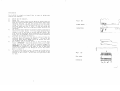
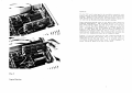
1 3CM ///M 3EM ///M 3CW ///M KM ///W 3CI 3CI I $ I U n ■ $ I u n I U 4 Disc User Manual I $ I U n ■ $ ■ u n I $ I I $ I u n I § ' m a k e it e a s y o n yourself 0 1 . 2 23 nmuimitmuimztmmmiLmmmiu May 83 ///■ U-4 Disc User Manual E-Microcomputers Ltd Winstanley Industrial Estate Long Lane Warrington Cheshire England U-Microcomputers Inc 300 Broad Street Stamford Connecticut 06901 USA Tlx Tel Tlx 965999 O&S STD Tel 203 359 4236 T.Free 800 243 2475 629279 U-MICRO G 0925 54117 1 Notice: This manual, the U-4DISC Card and the firmware supplied on the card are copyright (C) U-Microcomputers 1983. Manual issue A. 2 Introduction U-4DISC USER MANUAL The U-4DISC is a cost effective way of connecting up to four Apple Disc II or Disc II compatible disc drives to an Apple 11+, Apple //e or Apple compatible computer. It supplies both control signals, and power to the disc drive. Existing diskettes may be used without any change. Contents Intro (Auction Installation Operation Technical description Appendix 1 Source code listing of driver Appendix 2 Circuit diagram 4 3 Installation 1) 2) 3) 4) 5) 6) 7) Switch off the computer. Remove lid. Decide into which slots you are going to install the U-4 DISC main board (marked UFDC4) and auxiliary board (see operation section). To just test things and in most cases anyway the main U-4 DISC board will go into slot 6 and the auxiliary board into slot 5. NOTE: If only two drives are to be connected then the auxiliary board need not be installed. The auxiliary board should be received already connected by cable to the main board. If it has been detached then connect it now if you wish to use the auxiliary board. The wire from the auxiliary board connected to the pad just below the word "FRONT" printed on the board should be connected as indicated in Figure 1. Plug the main board into its chosen slot and then the auxiliary board as indicated in Figure 2. The end of the auxiliary board marked "FRONT" should be nearest the front (ie keyboard end) of the computer. Now connect from 1-4 disk drives to the U-4 DISC main board. I M P O R T A N T - the cable should stick out at right angles from the card if the cable is correctly plugged in. I M P O R T A N T - the plug must also be correctly inserted eg displacing the connector to the right or left so that some pins are not plugged in will damage the card or disc drive. Refer to figure 4. The card is now ready for use. On power up the disc drive attached to the connector marked "1" will switch on and attempt to boot a disc. To test the card just boot a DOS 3.3 dis c. Fig 1 (a) foliyiofel Paddle board connections Fig 1 (b) Disc cable connection 5 uf "V./x. The U-4DISC is simple to install but in case of difficulty consult your supplier. Operation The U-4 DISC card is designed to be completely compatible with Apple software written using DOS 3.3, UCSD or CP/M operating systems. Special or own written operating systems should also work satisfactorily provided their low level software operate in the same was as the above mentioned operating systems. These operating systems refer to the physical disc drives by different nomenclature . DOS 3.3 allows any slots to be used by disc drives whereas PASCAL and CP/M reserve slots for functions. Table 1 relates the drive designations to connectors on the U-4 DISC. For example if your CP/M program says - "Put diskette in drive C:" this means put the disc in the drive connected to connector 3 of the U-4 DISC main board. To make it easy the connectors are marked aswell. For all ready written software the table and this explanation should be all you need to know. However if you are writing new disk operating systems or enhancing existing ones beware that the U-4 DISC PROM is compatible but not the same inside. If your software enters at odd places things probably won t work. But don't despair. A source listing is given at the end of this manual. Fig 2 Installation 7 Table 1 U-4 DISC Slot 6 5 Disc Designations AUXILIARY board slot 5 4 Technical Description U-4 DISC DOS 3.3 connectors UCSD CP/M Introduction The U-FDC4 disk controller card in conjunction with a small paddle card in an adjacent peripheral expansion slots enables the user to control up to 4 floppy disk drives and is completely compatible with the Apple II 16 sector disk format. 1 S6, D1 #4: A: 2 S6, D2 #5: B: 3 S5, D1 #11: C: Operation 4 S5, D2 #12 D: 1 S5, DI E: Each slot of the Apple II is assigned to two floppy disk drives and the purpose of the small jumper pcb is to connect the NIOSEL and NDEVSEL signals from another slot into the U-FDC4 card which is typically installed in slot 6, This enables the card to control a total of four drives. 2 S5, D2 F: 3 S4, Dl na 4 S4, D2 na These two jumpered signals are OR'ed with the NIOSEL and NDEVSEL signals that are direct into the U-FDC4 card by means of the two 74LS08 AND gates. P2 is a 256 by 8 bit ROM which holds the Boot 0 program used by the computer monitor when the computer is switched on or reset. The monitor accesses this program at address CnOO which activates the NIOSEL line. The power to this ROM is conserved by the two pnp transistors which remove the +5v. line from the ROM while NIOSEL is inactive. The 556 is a dual timer. One half generates a reset pulse when power is applied, this signal is duplicating the reset signal generated on the main Apple II processor board. The other half is a monostable with a one second time constant. The output of this timer is used to enable the floppy drive motor and is constantly retriggered during a disk access which involves the transfer of many data bytes since data is accessed via NDEVSEL which is the timer trigger. The effect of this is to stop the drive motor and LED flashing on and off rapidly and also causes the motor to continue running for approXi one second after a disk access has been completed. The 74LS74 D-type flip flop is set and reset by the jumpered NDEVSEL or the direct NDEVSEL and indentifies which two of the four drives is being accessed. The 74LS259 is an addressable latch driven off the lower four bits of the address bus and enabled motor directly via four phases 00 to 03. It also controls selection of one of two drives. 9 Appendix 1 Source Code Listing Q5 of the LS259 and Q of the LS74 are decoded by the 74LS139 to select one of four drives by the NENO to NEN3 signals. The 74LS323 is a universal shift register operating as a parallel to serial register during a write cycle and as serial to parallel register during a disk read. Parallel data to or from this register is read or written by the Apple cpu over the data lines DO to D7. Data on format. encodes decodes holds a the floppy disk is held in a complex encoded serial PI and the 74LS174 form a state machine which either the serial data from the LS323 during a write cycle or during a read cycle. PI is a 256 by 8 bit ROM which series of encoding and decoding bit patterns. Q6 and Q7 of the LS259 select either a read or write cycle and control the direction of operation of both shift register and the state machine. The pnp transistors powers down both of the state machine ic s. while no disk accesses are taking place. i - i — -B * > > -k c^Ov*-|\3 h § 8 g 2 * C 10 -4s- !iV£ i"i SOURCE FILE: DISC CONTROLLER PROM ---- NEXT OBJECT FILE NAME IS DISC CONTROLLER PROM.OBJO OOOO: ORG $ 0 0 0 0 FF58: 2 IORTS EQU $FF58 0000:A9 20 3 LDA # $ 2 0 3 FIRST 8 BYTES MUST BE 0 0 0 2 :A 2 00 4 LDX # $ 0 0 ;$20,$??,$00,$??,$03,$??,$3C 0004:AO 03 5 LDY #$03 5 TO SATISFY AUTOSTART ROM 0006:84 3C 6 LI STY $3C 0008:06 3C 7 ASL $3C 5DYNAMICALLY BUILD READ TRANSLATE 000A:98 OOOB:25 3C OOOD-.FO 11 OOOF:98 0010:05 3C 0012:49 7E 0014:29 7E 0016:BO 08 0018:4A 0019:DO FB 0 0 1 B: 8 A 001C:99 56 03 0 0 1 F:E8 0 0 2 0 :C 8 0021:10 E3 0023:20 58 FF 0026:BA 0027:BD 00 01 002A:85 2C 0 0 2 C :OA 0 0 2 D:OA 0 0 2 E :OA 0 0 2 F :0 A 0030:AA 0031:86 2B 0033:5D 8 E CO 0036:5D SC CO 0039:ID 8 A CO 003C :ID 89 CO 003F:AO 80 0041:ID 80 CO 0044:98 MOTOR 0045:29 07 0047:05 2B 0049:AA OUTWARD 004A:5D 81 CO 004D:A9 56 004F:20 A8 FC 0052:88 0053:88 0054:10 EB 0056:85 3D 0058:A9 08 005A:85 27 8 23 24 25 26 27 28 29 30 31 32 33 34 35 36 37 38 L4 39 TYA AND $3C BEQ L3 TYA ORA $3C EOR #$7E AND #$7E BCS L3 LSR A BNE L2 TXA STA $0356,Y INX INY BPL LI JSR IORTS TSX LDA $ 1 0 0 ,X STA $2C ASL A ASL A ASL A ASL A TAX STX $2B EOR $C08E,X EOR $C08C,X ORA $C08A,X ORA $C089,X LDY #$80 ORA $C080,X TYA 40 41 42 AND ORA TAX #$07 $2B 43 44 45 46 47 48 49 50 51 EOR LDA JSR DEY DEY BPL STA LDA STA $C081,X #$56 $FCA8 9 10 11 12 13 14 15 L2 16 17 18 19 20 21 22 L3 L4 $3D #$08 $27 3 TABLE IN MEMORY FROM $3CD UPWARDS 5 FOR CONVERTING DISC BYTES TO 5 6 -BIT HEX -. .THI TABLE IS ARRANGED 5 SO THAT THE VALUE OF THE DISC BYTE 5CAN BE USED DIRECTLY AS A MODIFIER *OF'ER',X? ADDRESSING BELOW OBTAIN THE EQUIVALENT HEX CODE A SINGLE LOOKUP OPERATION 5 IN 5 TO 5 IN 5 FIND WHICH SLOT DISC CONTROLLER 5 CARD OCCUPIES 5 LOAD A WITH $CN WHERE N=SLOT NO 5 SOMETHING FOR BIT TO SET V WITH 5 MANUFACTURE $N0 5 AND PRESERVE FOR FUTURE USE 5 SELECT DRIVE 1,ENABLE READ 5 LATCH,TURN MOTOR ON 5 RECALIBRATE THE DISC BY 5 SEEKING OUTWARDS AT LEAST 40 5 EACH OF 4 PHASES 0-3 OF THE TRACKS STEPPEf 5 MUST BE TURNED ON THEN OFF. DONE IN 5 ASCENDING ORDER THIS SEEKS INWARD. 5 DONE IN DESCENDING ORDER THIS SEEK! 5 THIS CODE IS TIME-CRITICAL 5 MONITOR S/R TO WASTE 3 <26+27*A+5*A*A)/2 MICROSECS 005C: 005C s 005C: 005C: 005C:A9 00 005E :85 26 0060 s85 40 0062:B8 0063 sBD BL CO 0066:10 EB 0068:C9 D5 006A :DO F7 006C:BD SC CO 006F:10 FB 0071sC9 AA 0073:DO F3 0075:BD 8 C CO 0078:10 FB 007A :C9 96 007C:FO 08 007E :50 E3 0080:49 AD 0082:FO 26 0084:DO DC 0086:AO FD 0088:85 41 IVE 008A :BD 8 C CO RENTLY 008D:10 FB 008F:2A 0090:85 3C 0092:BD 8 C CO 0095:10 FB 0097:25 3C 0099:C8 009A:DO EC 009C:45 3D 009E:DO C 2 OOAO:A5 41 OOA2:45 40 00A4s DO BC 00A6:24 2C ODE 00A8:70 B9 OOAA:AO 56 00AC:84 3C OOAE:BC BC CO OOB 1 : 1 0 FB 00B3:59 D6 02 00B6;;C6 3C 00B8:A4 3C 00BA s99 00 03 OOBD:DO EF 00BF:BC BC CO 00C2:10 FB 7) 52 53 54 55 56 57 58 59 60 61 62 63 64 65 66 67 68 69 70 71 72 73 74 75 76 77 THE FOLLOWING CODE IS ALSO USED AS A SUBROUTINE BY THE 2ND STAGE BOOTSTRAP AND SO MUST BEGIN AT $5C LDA #0 STA $26 STA $40 3 TO $800 UPWARDS L5 CLV 5 WATCH READ DATA LATCH BIT 7 L6 LDA $C0BC,X 5 WHEN 1,DATA BYTE PRESENT BPL L 6 SIS IT START OF HEADER? L7 CMP #$D5 5 NO,KEEP LOOKING BNE L 6 ;POSSIBLY,WHAT?S NEX T? LB LDA $C08C,X BPL L 8 5 IS IT SECOND BYTE OF A HEADER? CMP #$AA 5 NO,TRY AGAIN BNE L7 LDA $C08C,X L9 BPL L9 SIS IT AN ADDRESS HEADER? CMP #$96 SYES BEQ L 10 5 1ST OR SECOND PASS THRU THIS CODE? BVC L6 3 ARE WE READING SECTOR DATA? EOR #$AD SYES BEQ L.14 SNO,TRY AGAIN BNE L.5 SHANDLE A SECTOR ADDRESS LDY #$FD L 10 3 READ IN 6 BYTES,AND COMBINE THEM TO G L 11 STA $41 * * * * 78 L 12 LDA $C08C,X SVOLUME,TRACK AND SECTOR OF SECTOR CUR 79 BPL POL STA LDA BPL AND INY BNE EOR BNE LDA EOR BNE BIT LI 2 A $3C $COBC,X L 13 $3C SBEING READ L1 1 $3D L5 $41 $40 L5 $2C 5 COMPARE BVS LDY STY LDY BPL EOR DEC LDY STA BNE LDY BPL L6 #$56 $3C $C08C,X LI 5 $02D6 ,Y $3C $3C $300,Y L15 $C08C,X L 16 80 81 82 L 13 83 84 85 86 87 88 89 90 91 92 93 94 1.14 95 96 L15 97 99 99 100 101 1 02 103 LI6 104 SECTOR FOUND WITH SECTOR SREQUIREDIF NO MATCH KEEP TRYING SDITTO TRACK 3 SET V--BIT TO INDICATE 2ND PASS THRU C 3 GET SECTOR DATA 3 READ 3 DATA IN 85 BYTES OF SECONDARY TO $300—$355 3 READ IN 256 BYTES OF PRIMARY DATA 3 TO ADDRESS AREA POINTED TO BY ($26,$2 00C4 :59 D6 00C7 sA4 3C 00C9:91 26 OOCBsCS OOCCs84 3C OOCEsDO EF OODO“BC SC 0 0 D3 s10 FB 00D5s 59 D6 00D8s DO 88 OODAs A8 00DB:A2 56 OODDsCA OODEs30 FB 00 EOs B 1 26 00E2:5E 00 00E5:2A 00E6:5E 00 00E9:2A OOEA s91 26 OOECs E6 26 00EE sDO ED OOFOsE6 27 00F2sE6 3D OOF4 sA5 3D OOFS:CD 00 OOF9:A6 2B TTE OOFBs90 DB OOFDs4C 01 AP 02 CO 02 03 03 08 08 105 106 107 108 109 123 124 125 126 127 128 129 130 131 EOR LDY STA INY STY BNE LDY BPL EOR BNE TAY LDX DEX BMI LDA LSR ROL LSR ROL STA INC BNE INC INC LDA CMP LDX L.19 ($26),Y $0300?X A $0300,X A ($26)„Y $26 L20 $27 $3D $3D $0800 $2B ;ARE MORE SECTORS TO BE READ? 5ONLY IF BOOTING FROM A 'BASICS' DISKE 132 133 BCC JMP LIS $0801 5START TO EXECUTE SECOND STAGE BOOTSTR 110 111 L 17 112 113 114 L 18 115 116 L 19 117 L20 118 119 120 121 122 $02D6,Y $3C ($26),Y $3C LI 6 $cosc,x L17 $02D6,Y L..5 Appendix 2 5VERIFY DATA SUMCHECK VALID #$56 5NIBBILISE PRIMARY AND SECONDARY ;DATA TOGETHER *** SUCCESSFUL ASSEMBLY!; NO ERRORS FF5S 8A BF 16 62 75 06 62 75 92 DO FF58 IORIS L12 L16 L2 L5 L9 LI L5 L9 L 13 L17 IORTS 06 92 DO DD 63 16 63 86 AA D8 LI L 13 LI 7 L20 L6 L2 L6 L 10 L 14 L18 86 AA D8 20 68 20 68 88 AE DB L.10 L14 L18 L3 L7 L3 L7 Lll L 15 L19 88 AE DB 41 6C 41 6C 8A BF DD L 11 L15 L 19 L4 L8 L4 L.8 L 12 L 16 L20 Circuit Diagram r mitmmuitmmmummmitmufmum/f/uiimmmu I u n I $ I u n U-Microcomputers Ltd. I Winstanley Industrial Estate, $ Long Lane, Warrington, Cheshire WA2 8PR I Telephone 0925-54117/8 u n Telex 629279 U M ICRO G I § I u n I I$ I u p« I I u PI I ■ u n ■ $ I ■ A I $ I I