1
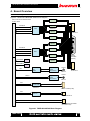
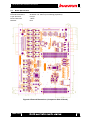
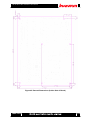
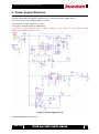
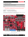
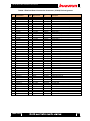
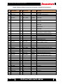
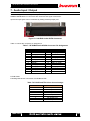
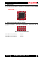
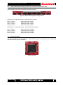
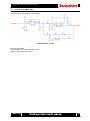
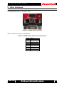
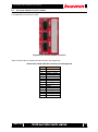
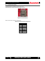
TB-EB-KN-AUDIO Hardware User Manual TB-EB-KN-AUDIO Hardware User Manual Rev.1.01 Rev.1.01 1 TB-EB-KN-AUDIO Hardware User Manual Revision History Version Date Description Publisher Rev.1.00 2012/09/27 Release version Amano Rev.1.01 2013/01/11 Modify Features Amano Rev.1.01 2 TB-EB-KN-AUDIO Hardware User Manual Table of Contents 1. 2. 3. 4. 5. 6. Related Documents and Accessories ......................................................................................... 9 Overview ...................................................................................................................................... 9 Features....................................................................................................................................... 9 Board Overview ......................................................................................................................... 10 4.1. Block Diagram ......................................................................................................................... 10 4.2. External View of Board .............................................................................................................11 4.3. Board Specification .................................................................................................................. 13 Power Supply Structure ............................................................................................................. 15 5.1. Pin Header Power Connector (CN101) ................................................................................... 16 5.2. DC Jack Power Connector (CN102) ....................................................................................... 16 Connectors and ICs ................................................................................................................... 17 6.1. 7. Audio Input / Output................................................................................................................... 20 7.1. D-SUB25 Audio AD/DA Connector (CN603) ........................................................................... 20 7.2. Pin Header Audio AD Connector (CN602) .............................................................................. 21 7.3. Audio AD Input Decoupling ...................................................................................................... 22 7.4. Audio AD Input Gain Setting (JP301, 302, 303, 304, 305, 306, 307 & 308) ........................... 22 7.5. Audio ADC (IC306) .................................................................................................................. 23 7.6. Audio AD Clip Display LEDs (LED203, 204, 205 & 206) ......................................................... 23 7.7. Pin Header Audio DA Connector (CN601) .............................................................................. 24 7.8. Audio DA Output Gain Setting (JP401, 402, 403, 404, 405, 406, 407 & 408) ........................ 25 7.9. Audio DAC (IC405) .................................................................................................................. 25 7.10. 8. 9. Platform Board Connection Connector (JP202, 203) .............................................................. 17 SPDIF Coaxial Input / Output Connector (CN701, 702) ...................................................... 26 Clock .......................................................................................................................................... 27 8.1. Onboard Clock (IC501, 510).................................................................................................... 27 8.2. Control 24.576 VCXO .............................................................................................................. 27 8.3. Control 22.5792MHz OSC ....................................................................................................... 28 Other Interfaces ......................................................................................................................... 29 9.1. D-SUB9 RS232C Connector (CN501) .................................................................................... 29 9.2. Pin Header RS485 Connector (CN502) .................................................................................. 30 9.3. microSD Socket (CN504) ........................................................................................................ 31 9.4. Pin Header Debug Connector (CN503) ................................................................................... 32 9.5. Debug LED (LED201, 202) ...................................................................................................... 32 10. Factory Default Board Settings ................................................................................................. 33 Rev.1.01 3 TB-EB-KN-AUDIO Hardware User Manual List of Figures Figure4-1 TB-EB-KN-AUDIO Block Diagram ................................................................................... 10 Figure4-2 External View of Board (Component Side) .......................................................................11 Figure4-3 External View of Board (Solder Side) .............................................................................. 12 Figure4-4 External Dimensions (Component Side of Board) ........................................................... 13 Figure4-5 External Dimensions (Solder Side of Board) ................................................................... 14 Figure5-1 Power Supply Circuit ....................................................................................................... 15 Figure5-2 Pin Header Power Connector Pin .................................................................................... 16 Figure5-3 DC Jack Power Connector .............................................................................................. 16 Figure6-1 Platform Board ................................................................................................................. 17 Figure7-1 D-SUB25 Audio AD/DA Connector .................................................................................. 20 Figure7-2 Pin Header Audio AD Connector ..................................................................................... 21 Figure7-3 Audio AD Input Gain Jumper Pins ................................................................................... 22 Figure7-4 ADC .................................................................................................................................. 23 Figure7-5 Audio AD Clip Display LEDs ............................................................................................ 23 Figure7-6 Pin Header Audio DA Connector ..................................................................................... 24 Figure7-7 Audio DA Output Gain Jumper Pins ................................................................................ 25 Figure7-8 DAC ................................................................................................................................. 25 Figure7-9 SPDIF Coaxial Input / Output Connector ......................................................................... 26 Figure 8-1 24.576MHz Clock ........................................................................................................... 27 Figure 8-2 22.5792MHz Clock ......................................................................................................... 27 Figure 8-3 VCXO Circuit................................................................................................................... 27 Figure 8-4 OSC circuit ...................................................................................................................... 28 Figure9-1 D-SUB9 RS232 Connector .............................................................................................. 29 Figure9-2 Pin Header RS-485 Connector ........................................................................................ 30 Figure9-3 microSD Socket ............................................................................................................... 31 Figure9-4 Pin Header Debug Connector.......................................................................................... 32 Figure9-5 Debug LEDs..................................................................................................................... 32 Figure10-1 Factory Default Board Settings ...................................................................................... 33 Rev.1.01 4 TB-EB-KN-AUDIO Hardware User Manual List of Tables Table5-1 Pin Header Power Connector Pin Assignment .................................................................. 16 Table5-2 DC Jack Power Connector Pin Assignment ...................................................................... 16 Table6-1 Platform Board Connection Connector (JP202) Pin Assignment ...................................... 18 Table6-2 Platform Board Connection Connector (JP203) Pin Assignment ...................................... 19 Table 7-1 D-SUB25 Audio AD/DA Connector Pin Assignment ......................................................... 20 Table 7-2 D-SUB and TRS in/out channel assign ............................................................................ 20 Table7-3 Pin Header Audio AD Connector Pin Assignment ............................................................. 21 Table7-4 Pin Header Audio DA Connector Pin Assignment ............................................................. 24 Table7-5 SPDIF Coaxial Input/Output Connector Pin Assignment .................................................. 26 Table9-1 D-SUB9 RS232C Connector Pin Assignment ................................................................... 29 Table9-2 Pin Header RS-485 Connector Pin Assignment................................................................ 30 Table9-3 microSD Socket Pin Assignment ....................................................................................... 31 Table9-4 Pin Header Debug Connector Pin Assignment ................................................................. 32 Table 9-5 LED201 Control ................................................................................................................ 32 Table 9-6 LED202 Control ................................................................................................................ 32 Table10-1 Factory Default Settings .................................................................................................. 33 Rev.1.01 5 TB-EB-KN-AUDIO Hardware User Manual Introduction Thank you for purchasing the TB-EB-KN-AUDIO board. Before using the product, be sure to carefully read this user manual and fully understand how to correctly use the product. First read through this manual, and then always keep it handy. SAFETY PRECAUTIONS Be sure to observe these precautions Observe the precautions listed below to prevent injuries to you or other personnel or damage to property. Before using the product, read these safety precautions carefully to assure correct use. These precautions contain serious safety instructions that must be observed. After reading through this manual, be sure to always keep it handy. The following conventions are used to indicate the possibility of injury/damage and classify precautions if the product is handled incorrectly. Danger Indicates the high possibility of serious injury or death if the product is handled incorrectly. Indicates the possibility of serious injury or death if the product is handled Warning incorrectly. Indicates the possibility of injury or physical damage in connection with houses or Caution household goods if the product is handled incorrectly. The following graphical symbols are used to indicate and classify precautions in this manual. (Examples) Turn off the power switch. Do not disassemble the product. ! Rev.1.01 Do not attempt this. 6 TB-EB-KN-AUDIO Hardware User Manual Warning In the event of a failure, disconnect the power supply. If the product is used as is, a fire or electric shock may occur. Disconnect the power supply immediately and contact our sales personnel for repair. If an unpleasant smell or smoking occurs, disconnect the power supply. If the product is used as is, a fire or electric shock may occur. immediately. Disconnect the power supply After verifying that no smoking is observed, contact our sales personnel for repair. Do not disassemble, repair or modify the product. Otherwise, a fire or electric shock may occur due to a short circuit or heat generation. For inspection, modification or repair, contact our sales personnel. ! Do not touch a cooling fan. As a cooling fan rotates in high speed, do not put your hand close to it. cause injury to persons. ! Otherwise, it may Never touch a rotating cooling fan. Do not place the product on unstable locations. Otherwise, it may drop or fall, resulting in injury to persons or failure. ! If the product is dropped or damaged, do not use it as is. ! Do not touch the product with a metallic object. ! Do not place the product in dusty or humid locations or where water may Otherwise, a fire or electric shock may occur. Otherwise, a fire or electric shock may occur. splash. Otherwise, a fire or electric shock may occur. ! ! Do not get the product wet or touch it with a wet hand. Otherwise, the product may break down or it may cause a fire, smoking or electric shock. Do not touch a connector on the product (gold-plated portion). Otherwise, the surface of a connector may be contaminated with sweat or skin oil, resulting in contact failure of a connector or it may cause a malfunction, fire or electric shock due to static electricity. Rev.1.01 7 TB-EB-KN-AUDIO Hardware User Manual Caution Do not use or place the product in the following locations. ! Humid and dusty locations Airless locations such as closet or bookshelf Locations which receive oily smoke or steam Locations exposed to direct sunlight Locations close to heating equipment Closed inside of a car where the temperature becomes high Staticky locations Locations close to water or chemicals Otherwise, a fire, electric shock, accident or deformation may occur due to a short circuit or heat generation. ! Do not place heavy things on the product. Otherwise, the product may be damaged. ■ Disclaimer This product is an evaluation board for Audio/FA application designed specifically for use with inrevium evaluation boards. Tokyo Electron Device Limited assumes no responsibility for any damages resulting from the use of this product for purposes other than those stated. Even if the product is used properly, Tokyo Electron Device Limited assumes no responsibility for any damages caused by: (1) Earthquake, thunder, natural disaster or fire resulting from the use beyond our responsibility, acts by a third party or other accidents, the customer’s willful or accidental misuse or use under other abnormal conditions. (2) Secondary impact arising from use of this product or its unusable state (business interruption or others) (3) Use of this product against the instructions given in this manual. (4) Malfunctions due to connection to other devices. Tokyo Electron Device Limited assumes no responsibility or liability for: (1) Erasure or corruption of data arising from use of this product. (2) Any consequences or other abnormalities arising from use of this product, or (3) Damage of this product not due to our responsibility or failure due to modification This product has been developed by assuming its use for research, testing or evaluation. It is not authorized for use in any system or application that requires high reliability. Repair of this product is carried out by replacing it on a chargeable basis, not repairing the faulty devices. However, non-chargeable replacement is offered for initial failure if such notification is received within two weeks after delivery of the product. The specification of this product is subject to change without prior notice. The product is subject to discontinuation without prior notice. Rev.1.01 8 TB-EB-KN-AUDIO Hardware User Manual 1. Related Documents and Accessories All documents relating to this board can be downloaded from our website Club-X. [Mounted accessory] Rubber foot: 4, Screw M3 x 6: 8, Spacer M3 x 10: 4 [Accessory] AC Adaptor (Akizuki Denshi: LTE(GFP)451DA-1238 [or equivalent]): 1 D-SUB Cable (HOSA: DTP802 [D-SUB25 to TRS]): 1 Jumper Socket (OMRON: XJ8A-0211): 8 2. Overview This product is an interface expansion board designed specifically for use with the inrevium evaluation board “TB-6S-LX25-FANET” (hereafter referred to as “platform board”). The board is intended for product design and evaluation purposes in audio/FA applications using Xilinx FPGA. It should be noted that the bank voltage (VCCO) of an FPGA on the platform board must be +3.3V. The board is equipped with 4-ch analog input/output and 2-ch digital input/output interfaces that are connected to high performance Analog to Digital Audio Converter (hereafter referred to as “ADC”) and Digital to Analog Audio Converter (hereafter referred to as “DAC”). It also provides RS232 and RS485 interfaces for connection to external devices and can support the demand for increasing storage capacity by adding microSD to the microSD sockets. (Tested SD-C02G[HAGIWARA SYS-COM]) 3. Features ADC Device: TI 192KHz/24bit PCM4204 DAC Device: TI 192KHz/24bit PCM4104 Input/Output Amplifier: TI OPA1632 Audio Clock (24.576MHz VCXO): Fox FVXO-HC73B-24.576 Audio Clock (22.5792MHz OSC): Kyocera KC7050B22.5792C3 D-SUB25 Audio AD/DA Connector: OMRON XM3B-2522-122 SPDIF Coaxial Input/Output Connector: Keystone Electronics 972 RS232C Driver Receiver: MAXIM MAX3243 RS485 Driver Receiver: TI SN65HVD33 MicroSD Socket: Hirose DM3AT-SF-PEJM5 Rev.1.01 9 TB-EB-KN-AUDIO Hardware User Manual 4. Board Overview 4.1. Block Diagram Figure 4-1 shows the TB-EB-KN-AUDIO block diagram. OpAmp DIP Connector for Platform Board JP202, JP203 OPA1632 ADC-BCK OpAmp ADC-LRCK ADC ADC-DOUT0 ADC-DOUT1 OPA1632 OpAmp PCM4204 CN602 B12B-XH-A OPA1632 OpAmp OPA1632 OpAmp OPA1632 DAC-BCK OpAmp DAC-LRCK DAC DAC-DIN0 DAC-DIN1 OpAmp PCM4104 24.576MHz 22.5792MHz OPA1632 VCXO CN603 D-SUB25 (female) OPA1632 OpAmp OPA1632 OSC Differential Bus Buffer DIN SN75176 DOUT+ Digital Audio Transformer MR-972 CN601 B12B-XH-A S37211 Digital Audio Transformer DOUT- CN701 CN702 MR-972 S37211 TXD RS232 Buffer RXD MAX3243 CN501 D-SUB9 (male) TXD RXD RS485 Buffer×3 SN65HVD CN502 B15B-XH-A CN504 DM3AT-SF-PEJM5 (microSD socket) Figure4-1 TB-EB-KN-AUDIO Block Diagram Rev.1.01 10 TB-EB-KN-AUDIO Hardware User Manual 4.2. External View of Board Figure 4-2 shows the external view of the TB-EB-KN-AUDIO board. Figure4-2 External View of Board (Component Side) Rev.1.01 11 TB-EB-KN-AUDIO Hardware User Manual Figure4-3 External View of Board (Solder Side) Rev.1.01 12 TB-EB-KN-AUDIO Hardware User Manual 4.3. Board Specification Figure 4-4 shows the TB-EB-KN-AUDIO board specification. External Dimensions: W:160mm x H:120mm (not including projections) Layer Structure: 6-Layer Board Thickness: 1.6mm Material: FR-4 Figure4-4 External Dimensions (Component Side of Board) Rev.1.01 13 TB-EB-KN-AUDIO Hardware User Manual Figure4-5 External Dimensions (Solder Side of Board) Rev.1.01 14 TB-EB-KN-AUDIO Hardware User Manual 5. Power Supply Structure Figure 5-1 shows the power supply circuit of the TB-EB-KN-AUDIO board. The board generates the following voltages from a +12V external power supply source: +13.0V/-13.0V from an LT power supply IC "LT3471" +5.0V from an LT power supply IC "LT1763" +3.3V from a TI power supply IC "LMZ14203" It should be noted that the bank voltage (VCCO) of an FPGA on the platform board (TB-6S-LX25-FANET) must be +3.3V. Figure5-1 Power Supply Circuit *AGND and DGND are connected. Rev.1.01 15 TB-EB-KN-AUDIO Hardware User Manual 5.1. Pin Header Power Connector (CN101) The board uses a JST B4P-VH-FB-B pin header power connector. Caution: Do not connect a CN102 simultaneously. Otherwise, the board components may be damaged. Be sure to use either one of these power connectors for power feeding. Figure5-2 Pin Header Power Connector Pin Table 5-1 shows the connector pin assignment. Table5-1 Pin Header Power Connector Pin Assignment 5.2. Pin # Name 1 +12V 2 GND 3 +12V 4 GND DC Jack Power Connector (CN102) An AC adaptor comes with the board. The board uses a CUI PJ-002AH DC jack power connector. Caution: Do not connect a CN101 simultaneously. Otherwise, the board components may be damaged. Be sure to use either one of these power connectors for power feeding. Figure5-3 DC Jack Power Connector Table 5-2 shows the connector pin assignment. Table5-2 DC Jack Power Connector Pin Assignment Rev.1.01 Pin # Name 1 +12V 2 GND 3 GND 16 TB-EB-KN-AUDIO Hardware User Manual 6. Connectors and ICs 6.1. Platform Board Connection Connector (JP202, 203) This is a Samtec TSM-122-01-L-DV-A connector used to connect the TB-6S-LX25-FANET platform board. Caution: When inserting or removing the connector, some of the connector pins may become bent or broken. It is recommended not to insert or remove the connector frequently. The Direction field in the table shows a signal direction: Direction = I Platform Board to TB-EB-KN-AUDIO (Input) Direction = O TB-EB-KN-AUDIO to Platform Board (Output) For information on FPGA pin assignment of the TB-6S-LX25-FANET Platform Board, refer to the web site for board purchasers (“Master UCF File” or “Platform Board Circuit”). Figure6-1 Platform Board The subsequent pages show the connector pin assignments. Rev.1.01 17 TB-EB-KN-AUDIO Hardware User Manual Table6-1 Platform Board Connection Connector (JP202) Pin Assignment Pin # TB-6S-LX25-FANET CN2 Pin Name DIR Signal Name Connecting to Description 1 2 3 4 5 6 7 8 9 10 11 12 13 14 15 16 17 18 19 20 21 22 23 24 25 26 27 28 29 30 31 32 33 34 35 36 37 38 39 40 41 42 43 44 USER_3P3V uC_DAT_ENA uC_ADR0 GND uC_ADR1 uC_nBUSY uC_ADR2 uC_nIRQ uC_ADR3 uC_nCS uC_ADR4 uC_DATA0 uC_ADR5 uC_DATA1 uC_ADR6 uC_DATA2 uC_ADR7 uC_DATA3 uC_ADR8 uC_DATA4 uC_ADR9 uC_DATA5 uC_ADR10 uC_DATA6 uC_ADR11 uC_DATA7 uC_ADR12 uC_DATA8 uC_ADR13 uC_DATA9 uC_ADR14 uC_DATA10 uC_ADR15 uC_DATA11 uC_EMULATION uC_DATA12 uC_nBHE uC_DATA13 uC_nRD uC_DATA14 uC_nWR GND USER_3P3V uC_DATA15 I O I I O I I I O I I O O O I O I O I O I I I I I I I O I/O I I/O I O I I I/O I I/O I/O +3.3VD DAC_0_FMT0 TTL1RXD GND TTL1TXD DAC_0_FMT1 TTL2RXD DAC_0_FMT2 TTL2TXD DAC_0_FS0 TTL3RXD DAC_0_FS1 TTL3TXD TTL0RXD TTL4RXD TTL0DSR TTL4TXD TTL0DCD TTL1RE TTL0CTS TTL1DE TTL0RI TTL2RE TTL0TXD TTL2DE TTL0RTS TTL3RE TTL0DTR TTL3DE DIN SD_DAT2 DOUT+ SD_DAT1 DOUTSD_SW SD_CLK LED1_1 SD_CMD LED1_2 SD_DAT3 NC GND +3.3V SD_DAT0 IC405(25) IC504(2) IC504(5) IC405(26) IC505(2) IC405(27) IC505(5) IC405(28) IC506(2) IC405(29) IC506(5) IC503(19) CN503(1) IC503(18) CN503(2) IC503(17) IC504(3) IC503(16) IC504(4) IC503(15) IC505(3) IC503(14) IC505(4) IC503(13) IC506(3) IC503(12) IC506(4) IC701(1) CN504(1) CN702(2) CN504(8) CN702(1) CN504(A) CN504(5) LED201(4) CN504(3) LED201(2) CN504(2) CN504(7) +3.3V Power (to Platform Board) PCM4104 Audio Data Format Configuration SN65HVD33 R Ground SN65HVD33 D PCM4104 Audio Data Format Configuration SN65HVD33 R PCM4104 Audio Data Format Configuration SN65HVD33 D PCM4104 Sampling Mode Configuration SN65HVD33 R PCM4104 Sampling Mode Configuration SN65HVD33 D MAX3243 R1OUT Debug Connector Pin 1 MAX3243 R2OUT Debug Connector Pin 2 MAX3243 R3OUT SN65HVD33 RE (Active Low) MAX3243 R4OUT SN65HVD33 DE MAX3243 R5OUT SN65HVD33 RE (Active Low) MAX3243 T1IN SN65HVD33 DE MAX3243 T2IN SN65HVD33 RE (Active Low) MAX3243 T3IN SN65HVD33 DE Digital Audio Input microSD DATA2 Digital Audio Output P microSD DATA1 Digital Audio Output N microSD SW-A microSD Clock 2-color type LED Green (Active Low) microSD CMD 2-color type LED Red (Active Low) microSD DATA3/CD Non Connect Ground +3.3V Power (to Platform Board) microSD DATA0 Rev.1.01 18 TB-EB-KN-AUDIO Hardware User Manual Table6-2 Platform Board Connection Connector (JP203) Pin Assignment Pin # TB-6S-LX25-FANET CN3 Pin Name DIR Signal Name Connecting to 1 USR_IOP0 O ADC_0_CLIP1 IC306(34) 2 3 USER_3P3V GND - +3.3V GND - 4 USR_IOP10 I ADC_0_HPFD IC306(38) 5 USR_ION0 O ADC_0_DOUT1 IC306(32) 6 USR_ION10 O ADC_0_CLIP4 IC306(37) 7 USR_IOP1 O ADC_0_DOUT0 IC306(31) 8 USR_IOP11 O ADC_0_CLIP3 IC306(36) 9 USR_ION1 I ADC_0_LRCK IC306(30) 10 USR_ION11 O ADC_0_CLIP2 IC306(35) 11 USR_IOP2 I ADC_0_BCK IC306(29) 12 USR_IOP12 I DAC_0_MODE IC405(8) 13 14 15 16 17 18 USR_ION2 USR_ION12 USR_IOP3 USR_IOP13 USR_ION3 USR_ION13 I I I I I I ADC_0_FMT2 DAC_0_RST ADC_0_FMT1 DAC_0_MUTE ADC_0_FMT0 DAC_0_SCKI IC306(20) IC405(9) IC306(19) IC405(10) IC306(18) IC405(14) 19 USR_IOP4 I ADC_0_SM IC306(17) 20 21 22 23 24 25 26 27 28 USR_IOP14 USR_ION4 USR_ION14 USR_IOP5 USR_IOP15 USR_ION5 USR_ION15 USR_IOP6 USR_IOP16 I I I I I I I I I DAC_0_BCK ADC_0_SCKI DAC_0_LRCK ADC_0_FS2 DAC_0_DIN0 ADC_0_FS1 DAC_0_DIN1 ADC_0_FS0 DAC_0_CS IC405(15) IC306(15) IC405(16) IC306(14) IC405(17) IC306(13) IC405(18) IC306(12) IC405(21) 29 USR_ION6 I ADC_0_RST IC306(10) 30 31 32 33 34 35 36 37 38 39 40 41 42 43 44 USR_ION16 USR_IOP7 USR_CLK_P USR_ION7 USR_CLK_N SYNC_OUT0 MOTH_MOSI SYNC_OUT1 MOTH_DIN LATCH_IN0 MOTH_XCS GND MOTH_CCLK LATCH_IN1 USER_3P3V I O I O O I I I I - DAC_0_CCLK CLK_24P576 DAC_0_CDTI CLK_22P579 DAC_0_CDTO VCXO_CTRL0 NC VCXO_CTRL1 NC LED2_1 NC NC LED2_2 +3.3V IC405(22) IC501(4) IC405(23) IC510(3) IC405(24) IC507(3) IC508(3) LED202(4) LED202(2) - Rev.1.01 Description PCM4204 Channel 1 Clipping Flag (Active High) +3.3V Power (to Platform Board) Ground PCM4204 High-Pass Filter Disable (Active High) PCM4204 PCM Data for Channels 3 and 4 PCM4204 Channel 4 Clipping Flag (Active High) PCM4204 PCM Data for Channels 1 and 2 PCM4204 Channel 3 Clipping Flag (Active High) PCM4204 Audio Serial Port Left/Right (or Word) Clock PCM4204 Channel 2 Clipping Flag (Active High) PCM4204 Audio Serial Port Bit Clock PCM4104 Operating Mode (0 = Standalone, 1= Software Controlled) PCM4204 Audio Data Format PCM4104 Reset/Power Down (Active Low) PCM4204 Audio Data Format PCM4104 All−Channel Soft Mute (Active High) PCM4204 Audio Data Format PCM4104 System Clock PCM4204 Audio Serial Port Slave/Master Mode (0 = Master, 1 = Slave) PCM4104 Audio Bit (or Data) Clock PCM4204 System Clock PCM4104 Audio Left/Right (or Word) Clock PCM4204 Sampling Mode PCM4104 Audio Data for Channels 1 and 2 PCM4204 Sampling Mode PCM4104 Audio Data for Channels 3 and 4 PCM4204 Sampling Mode PCM4104 SPI Chip Select (Active Low) PCM4204 Reset/Power Down (Active Low with internal pull-up to VDD1) PCM4104 SPI Data Clock VCXO 24.576MHz Input PCM4104 SPI Data Input 22.579MHz Input PCM4104 SPI Data Output VCXO 0 VC No connect VCXO 1 VC No connect 2-color type LED Green (Active Low) No connect Ground No connect 2-color type LED Red (Active Low) +3.3V Power (to Platform Board) 19 TB-EB-KN-AUDIO Hardware User Manual 7. Audio Input / Output 7.1. D-SUB25 Audio AD/DA Connector (CN603) The board supports 4ch analog audio inputs and outputs. OMRON XM3B-2522-112 connectors are used for these signal connections. Input and output gains can be controlled by setting onboard jumper pins. Figure7-1 D-SUB25 Audio AD/DA Connector Table 7-1 shows the connector pin assignment. Table 7-1 D-SUB25 Audio AD/DA Connector Pin Assignment Pin # 1 2 3 4 5 6 7 8 9 10 11 12 13 Name DAC_0_VOUT4+ AGND DAC_0_VOUT3DAC_0_VOUT2+ AGND DAC_0_VOUT1ADC_0_VIN4+ AGND ADC_0_VIN3ADC_0_VIN2+ AGND ADC_0_VIN1NC Pin # 14 15 16 17 18 19 20 21 22 23 24 25 - Name DAC_0_VOUT4DAC_0_VOUT3+ AGND DAC_0_VOUT2DAC_0_VOUT1+ AGND ADC_0_VIN4ADC_0_VIN3+ AGND ADC_0_VIN2ADC_0_VIN1+ AGND - D-SUB Cable Following table shows connection of D-SUB and TRS. Table 7-2 D-SUB and TRS in/out channel assign TRS No. 1 2 3 4 5 6 7 8 Rev.1.01 Connect to AD Input CH1 AD Input CH2 AD Input CH3 AD Input CH4 DA Output CH1 DA Output CH2 DA Output CH3 DA Output CH4 20 TB-EB-KN-AUDIO Hardware User Manual 7.2. Pin Header Audio AD Connector (CN602) All analog audio inputs are connected to the JST B12B-XH-A connector in a multipoint connection. Figure7-2 Pin Header Audio AD Connector Table 7-3 shows the connector pin assignment. Table7-3 Pin Header Audio AD Connector Pin Assignment Pin # 1 2 3 4 5 6 7 8 9 10 11 12 Rev.1.01 Name ADC_0_VIN1+ ADC_0_VIN1AGND ADC_0_VIN2+ ADC_0_VIN2AGND ADC_0_VIN3+ ADC_0_VIN3AGND ADC_0_VIN4+ ADC_0_VIN4AGND 21 TB-EB-KN-AUDIO Hardware User Manual 7.3. Audio AD Input Decoupling The audio inputs decoupling capacitors are inserted in series. 7.4. Audio AD Input Gain Setting (JP301, 302, 303, 304, 305, 306, 307 & 308) A desired audio input gain is selectable using these jumper pins. Figure7-3 Audio AD Input Gain Jumper Pins Rated Input + 4dBu, Max Input + 18dBu (balanced inputs): ADC_0_VIN1: ADC_0_VIN2: ADC_0_VIN3: ADC_0_VIN4: JP301 and JP302 = SHORT. JP303 and JP304 = SHORT. JP305 and JP306 = SHORT. JP307 and JP308 = SHORT. Rated Input - 10dBV, Max Input + 4dBV (unbalanced inputs): ADC_0_VIN1: ADC_0_VIN2: ADC_0_VIN3: ADC_0_VIN4: Rev.1.01 JP301 and JP302 = OPEN. JP303 and JP304 = OPEN. JP305 and JP306 = OPEN. JP307 and JP308 = OPEN. 22 TB-EB-KN-AUDIO Hardware User Manual 7.5. Audio ADC (IC306) The board is equipped with a TI PCN4204 device that supports 24bit/192kHz ADC. 4ch analog audio inputs are supported. These audio inputs are connected to the onboard CN602/603 connectors via a TI OPA1632. Caution: DSDCLK (24), DSD1 (25), DSD2 (26), DSD3 (27) and DSD4 (28) are NC and SUB (39) is connected to GND. Figure7-4 ADC 7.6. Audio AD Clip Display LEDs (LED203, 204, 205 & 206) The following four audio AD clip display LEDs are provided that can be controlled from the ADC state display pin. Figure7-5 Audio AD Clip Display LEDs LED203: LED204: LED205: LED206: State of a clip in Channel 1 State of a clip in Channel 2 State of a clip in Channel 3 State of a clip in Channel 4 Rev.1.01 Clip = ON Clip = ON Clip = ON Clip = ON 23 TB-EB-KN-AUDIO Hardware User Manual 7.7. Pin Header Audio DA Connector (CN601) All analog audio outputs are connected to the JST B12B-XH-A connector in a multipoint connection. Figure7-6 Pin Header Audio DA Connector Table 7-4 shows the connector pin assignment. Table7-4 Pin Header Audio DA Connector Pin Assignment Pin # 1 2 3 4 5 6 7 8 9 10 11 12 Rev.1.01 Name DAC_0_VOUT1+ DAC_0_VOUT1AGND DAC_0_VOUT2+ DAC_0_VOUT2AGND DAC_0_VOUT3+ DAC_0_VOUT3AGND DAC_0_VOUT4+ DAC_0_VOUT4AGND 24 TB-EB-KN-AUDIO Hardware User Manual 7.8. Audio DA Output Gain Setting (JP401, 402, 403, 404, 405, 406, 407 & 408) A desired audio output gain is selectable using these jumpers. Figure7-7 Audio DA Output Gain Jumper Pins Rated Output + 4dBu, Max Output + 18dBu (balanced outputs): DAC_0_VOUT1: DAC_0_VOUT2: DAC_0_VOUT3: DAC_0_VOUT4: JP401 and JP402 = OPEN. JP403 and JP404 = OPEN. JP405 and JP406 = OPEN. JP407 and JP408 = OPEN. Rated Output - 10dBV, Max Output + 4dBV (unbalanced Outputs): DAC_0_VOUT1: DAC_0_VOUT2: DAC_0_VOUT3: DAC_0_VOUT4: JP401 and JP402 = SHORT. JP403 and JP404 = SHORT. JP405 and JP406 = SHORT. JP407 and JP408 = SHORT. 7.9. Audio DAC (IC405) The board is equipped with a TI PCN4104 device that supports 24bit/192kHz DAC. 4ch analog audio outputs are supported. These audio outputs are connected to the CN601/603 onboard connectors via a TI OPA1632. Figure7-8 DAC Rev.1.01 25 TB-EB-KN-AUDIO Hardware User Manual 7.10. SPDIF Coaxial Input / Output Connector (CN701, 702) The SPDIF Transmitter/Receiver in the FPGA of the Platform Board can be used for digital audio inputs and outputs. A Keystone Electronics 972 connector is used for this configuration. The CN701 input pin is terminated with 75-ohms. Figure7-9 SPDIF Coaxial Input / Output Connector Table 7-5 shows the connector pin assignment. Table7-5 SPDIF Coaxial Input/Output Connector Pin Assignment Pin # CN701:1 CN701:2 CN701:3 Rev.1.01 Name DGND DIN NC Pin # CN702:1 CN702:2 CN702:3 Name DGND DOUT NC 26 TB-EB-KN-AUDIO Hardware User Manual 8. Clock 8.1. Onboard Clock (IC501, 510) The board provides the following two onboard clock sources: 24.576MHz (VCXO), 22.5792MHz (FIX) The VCXO enables self-oscillation and synchronization with external clock sources (48-kHz only). Figure 8-1 24.576MHz Clock Figure 8-2 22.5792MHz Clock 8.2. Control 24.576 VCXO 24.576 VCXO(IC501) has a Low Path Filer(LPF) circuit to the frequency control pin(VC). The frequency is adjustable by PWM control method from a FPGA to signal “VCXO_CTRL0”. Figure 8-3 VCXO Circuit The frequency is control -150PPM to +150PPM area by 0 to 3.3V voltage. (VC= 1.65: 24.576MHZ) Please refer to the reference design for PWM control method. Also, refer to the datasheet of VCXO(FVXO-HC73B-24.576) http://www.foxonline.com/pdfs/FVXO_HC73.pdf About 24.576 OSC This board can use OSC instead of VCXO. Please contact us if using OSC. Rev.1.01 27 TB-EB-KN-AUDIO Hardware User Manual 8.3. Control 22.5792MHz OSC OSC is controlled by signal “VCXO_CTRL1” form FPGA. VCXO_CTRL1: High- Enable, Low- Disable. Figure 8-4 OSC circuit About 24.576 VCXO This board can use VCXO instead of OSC. Please contact us if using VCXO. Rev.1.01 28 TB-EB-KN-AUDIO Hardware User Manual 9. Other Interfaces 9.1. D-SUB9 RS232C Connector (CN501) This is a RS-232C interface using MAXIM MAX3243. An OMRON XM3C-0922-112 connector is used. Figure9-1 D-SUB9 RS232 Connector Table 9-1 shows the connector pin assignment. Table9-1 D-SUB9 RS232C Connector Pin Assignment Pin # 1 2 3 4 5 6 7 8 9 Rev.1.01 Name RS232C0 DCD RS232C0 RXD RS232C0 TXD RS232C0 DTR DGND RS232C0 DSR RS232C0 RTS RS232C0 CTS RS232C0 RI 29 TB-EB-KN-AUDIO Hardware User Manual 9.2. Pin Header RS485 Connector (CN502) This is tree RS-485 interfaces using TI SN65HVD33. A JST B15B-XH-A connector is used. Figure9-2 Pin Header RS-485 Connector Table 9-2 shows the Pin Header RS-485 connector pin assignment. Table9-2 Pin Header RS-485 Connector Pin Assignment Pin # 1 2 3 4 5 6 7 8 9 10 11 12 13 14 15 Rev.1.01 Name RS422_1_RXD+ RS422_1_RXDRS422_1_TXD+ RS422_1_TXDDGND RS422_2_RXD+ RS422_2_RXDRS422_2_TXD+ RS422_2_TXDDGND RS422_3_RXD+ RS422_3_RXDRS422_3_RXD+ RS422_3_RXDDGND 30 TB-EB-KN-AUDIO Hardware User Manual 9.3. microSD Socket (CN504) Making up a controller using the FPGA on the Platform Board allows the use of a microSD card. A HIROSE DM3AT-SF-PEJM5 microSD socket is used. HAGIWARA SYS-COM SD-C02(microSD 2GB) is mounted. Figure9-3 microSD Socket Table 9-3 shows the connector pin assignment. Table9-3 microSD Socket Pin Assignment Pin # 1 2 3 4 5 6 7 8 A B Rev.1.01 Name SD_DAT2 SD_DAT3 SD_CMD +3.3VD SD_CLK DGND SD_DAT0 SD_DAT1 SD_SW DGND 31 TB-EB-KN-AUDIO Hardware User Manual 9.4. Pin Header Debug Connector (CN503) This is a multi-purpose pin header connected directly to the Platform Board. A JST B3B-XH-A connector is used. Figure9-4 Pin Header Debug Connector Table 9-4 shows the connector pin assignment. Table9-4 Pin Header Debug Connector Pin Assignment Pin # 1 2 3 Name TTL4RXD TTL4TXD DGND 9.5. Debug LED (LED201, 202) These are multi-purpose LEDs connected directly to the Platform Board. A 2-color Rohm SML-522MUW light emitting diode is used. Figure9-5 Debug LEDs Table 9-5 LED201 Control Pin # 37 39 TB-6S-LX25-FANET CN2 Pin Name uC_nBHE uC_nRD DIR I I Signal Name LED1_1 LED1_2 Connected to LED201(4) LED201(2) Description Green: Low Active Red: Low Active Table 9-6 LED202 Control Pin # 39 43 TB-6S-LX25-FANET CN3 Pin Name LATCH_IN0 LATCH_IN1 Rev.1.01 DIR I I Signal Name LED2_1 LED2_2 Connected to LED202(4) LED202(2) Description Green: Low Active Red: Low Active 32 TB-EB-KN-AUDIO Hardware User Manual 10. Factory Default Board Settings No.1 – 8 : SHORT No.9 – 16 : SHORT Figure10-1 Factory Default Board Settings Table10-1 Factory Default Settings No. Silk No. Initial Setting Function 1 JP301 SHORT Rated Input + 4dBu, Max Input + 18dBu (balanced inputs) 2 JP302 SHORT Rated Input + 4dBu, Max Input + 18dBu (balanced inputs) 3 4 5 6 7 8 9 10 11 12 13 14 15 16 JP303 JP304 JP305 JP306 JP307 JP308 JP401 JP402 JP403 JP404 JP405 JP406 JP407 JP408 SHORT SHORT SHORT SHORT SHORT SHORT OPEN OPEN OPEN OPEN OPEN OPEN OPEN OPEN Rated Input + 4dBu, Max Input + 18dBu (balanced inputs) Rated Input + 4dBu, Max Input + 18dBu (balanced inputs) Rated Input + 4dBu, Max Input + 18dBu (balanced inputs) Rated Input + 4dBu, Max Input + 18dBu (balanced inputs) Rated Input + 4dBu, Max Input + 18dBu (balanced inputs) Rated Input + 4dBu, Max Input + 18dBu (balanced inputs) Rated Output + 4dBu, Max Output + 18dBu (balanced outputs) Rated Output + 4dBu, Max Output + 18dBu (balanced outputs) Rated Output + 4dBu, Max Output + 18dBu (balanced outputs) Rated Output + 4dBu, Max Output + 18dBu (balanced outputs) Rated Output + 4dBu, Max Output + 18dBu (balanced outputs) Rated Output + 4dBu, Max Output + 18dBu (balanced outputs) Rated Output + 4dBu, Max Output + 18dBu (balanced outputs) Rated Output + 4dBu, Max Output + 18dBu (balanced outputs) Rev.1.01 33 TB-EB-KN-AUDIO Hardware User Manual PLD Solution Dept. PLD Division URL: http://solutions.inrevium.com/ E-mail: [email protected] HEAD Quarter: Yokohama East Square, 1-4 Kinko-cho, Kanagawa-ku, Yokohama City, Kanagawa, Japan 221-0056 TEL: +81-45-443-4016 FAX: +81-45-443-4058 Rev.1.01 34