1
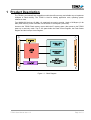
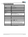
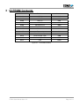
The Embedded I/O Company
TIP250
8 Mbytes Flash Memory
Version 1.0
User Manual
Issue 1.2
October 2008
TEWS TECHNOLOGIES GmbH
Am Bahnhof 7
Phone: +49-(0)4101-4058-0
25469 Halstenbek, Germany
Fax: +49-(0)4101-4058-19
www.tews.com
e-mail: [email protected]
TEWS TECHNOLOGIES LLC
9190 Double Diamond Parkway,
Suite 127, Reno, NV 89521, USA
www.tews.com
Phone: +1 (775) 850 5830
Fax: +1 (775) 201 0347
e-mail: [email protected]
TIP250-10
8 Mbytes Flash Memory
This document contains information, which is
proprietary to TEWS TECHNOLOGIES GmbH. Any
reproduction without written permission is forbidden.
TEWS TECHNOLOGIES GmbH has made any
effort to ensure that this manual is accurate and
complete. However TEWS TECHNOLOGIES GmbH
reserves the right to change the product described
in this document at any time without notice.
TEWS TECHNOLOGIES GmbH is not liable for any
damage arising out of the application or use of the
device described herein.
Style Conventions
Hexadecimal characters are specified with prefix 0x,
i.e. 0x029E (that means hexadecimal value 029E).
For signals on hardware products, an ‚Active Low’ is
represented by the signal name with # following, i.e.
IP_RESET#.
Access terms are described as:
W
Write Only
R
Read Only
R/W
Read/Write
R/C
Read/Clear
R/S
Read/Set
©2001 -2008 by TEWS TECHNOLOGIES GmbH
All trademarks mentioned are property of their respective owners.
TIP250 User Manual Issue 1.2
Page 2 of 11
Issue
Description
Date
1.0
First Issue
December 2001
1.1
Added MTBF Value
January 2002
1.2
Added Weight
New Address TEWS LLC
October 2008
TIP250 User Manual Issue 1.2
Page 3 of 11
Table of Contents
1
2
3
4
PRODUCT DESCRIPTION ........................................................................................... 6
TECHNICAL SPECIFICATION ..................................................................................... 7
ID PROM CONTENTS................................................................................................... 8
IP ADDRESSING .......................................................................................................... 9
4.1 I/O Addressing.................................................................................................................................9
4.1.1
Flash Control Register (FCR) ...................................................................................................9
4.1.2
Flash Status Register (FSR)...................................................................................................10
4.1.3
Interrupt Vector Register (IVR) ...............................................................................................10
4.2 Memory Addressing......................................................................................................................10
5
HINTS.......................................................................................................................... 11
5.1
5.2
Flash Memory ................................................................................................................................11
JTAG Connector............................................................................................................................11
TIP250 User Manual Issue 1.2
Page 4 of 11
Table of Figures
FIGURE 1-1 : BLOCK DIAGRAM......................................................................................................................6
FIGURE 2-1 : TECHNICAL SPECIFICATION...................................................................................................7
FIGURE 3-1 : ID PROM CONTENTS ...............................................................................................................8
FIGURE 4-1 : REGISTER SET .........................................................................................................................9
FIGURE 4-2 : FLASH CONTROL REGISTER ..................................................................................................9
FIGURE 4-3 : FLASH STATUS REGISTER ...................................................................................................10
FIGURE 4-4 : INTERRUPT VECTOR REGISTER..........................................................................................10
FIGURE 4-5 : MEMORY STRUCTURE ..........................................................................................................10
FIGURE 5-1 : TYPICAL FLASH ACCESS TIMES ..........................................................................................11
FIGURE 5-2 : JTAG CONNECTOR ................................................................................................................11
TIP250 User Manual Issue 1.2
Page 5 of 11
1 Product Description
The TIP250 is an IndustryPack compatible module that offers an easy and reliable way to implement
8 Mbytes of Flash memory. The TIP250 is ideal for holding application code, operating system
software or data.
Two AM29LV033 devices (32 Mbit, x 8 organized) are used to provide 1 bank of 8 Mbytes (16 bit
wide) Flash memory, which is divided, into 64 sectors of 128 Kbytes (16 bit wide).
Access to the TIP250 Flash memory occurs within the IP memory space. After power-on the TIP250
starts up in read only mode. The IP I/O space holds the Flash Control Register, the Flash Status
Register and the Interrupt Vector Register.
Figure 1-1 : Block Diagram
TIP250 User Manual Issue 1.2
Page 6 of 11
2 Technical Specification
IP Interface
Interface
Single Size IndustryPack® Logic Interface compliant to
ANSI/VITA 4-1995
ID ROM Data
Format I
I/O Space
Used, with no wait states
Memory Space
8 MByte, with 1 wait state
Interrupts
Only INTREQ0# is used
DMA
Not supported
Clock Rate
8 MHz
Module Type
Type I
On Board Devices
Memory
8 MBytes Flash Memory (4 Mbit x 16), implemented by two
AM29LV033 (or compatible).
Organized as 64 sectors of 128 KBytes
Min. erase and program cycle endurance: 1 000 000
I/O Interface
no connection to the IP I/O connector
Power Requirements
160 mA typical @ +5V DC
Physical Data
Temperature Range
Operating
Storage
MTBF
407000 h
-40 °C to +85 °C
-55°C to +125°C
MTBF values shown are based on calculation according to MIL-HDBK-217F
and MIL-HDBK-217F Notice 2; Environment: GB 20°C.
The MTBF calculation is based on component FIT rates provided by the
component suppliers. If FIT rates are not available, MIL-HDBK-217F and
MIL-HDBK-217F Notice 2 formulas are used for FIT rate calculation.
Humidity
5 – 95 % non-condensing
Weight
25 g
Figure 2-1 : Technical Specification
TIP250 User Manual Issue 1.2
Page 7 of 11
3 ID PROM Contents
Address
Function
Contents
0x01
ASCII ‘I’
0x49
0x03
ASCII ‘P’
0x50
0x05
ASCII ‘A’
0x41
0x07
ASCII ‘C’
0x43
0x09
Manufacturer ID
0xB3
0x0B
Model Number
0x30
0x0D
Revision
0x10
0x0F
Reserved
0x00
0x11
Driver-ID Low - Byte
0x00
0x13
Driver-ID High - Byte
0x00
0x15
Number of bytes used
0x0C
0x17
CRC
0xFD
Figure 3-1 : ID PROM Contents
TIP250 User Manual Issue 1.2
Page 8 of 11
4 IP Addressing
The control registers of the TIP250 are accessible in the IP I/O Space.
The Flash memory of the TIP250 is accessible in the IP MEM Space.
4.1 I/O Addressing
The complete register set of the TIP250 is accessible in the I/O space of the IP.
Address
Symbol
Description
Size (Bit)
Access
0x01
FCR
Flash Control Register
8
R/W
0x03
FSR
Flash Status Register
8
R/W
0x05
IVR
Interrupt Vector Register
8
R/W
Figure 4-1 : Register Set
4.1.1 Flash Control Register (FCR)
Read/Write Register to control basic features of the TIP250.
Bit
Symbol
Description
Access
Reset
Value
7
F_RST
Reset flash memory
Writing a “1” forces the Flash Memory into reset. A
subsequently written "0" terminates the reset. Reset forces the
flash memory into read-only state. Refer to the AM29LV033
data sheet for more details.
R/W
0
6
WP
Write Protect (active high)
0 = no write protection
1 = write protected (default after Reset)
R/W
1
5
INT_EN
Interrupt Enable
0 = interrupt disabled
1 = An interrupt is generated on IP INTREQ0# when the flash
memory's state changes from BUSY to READY during WRITE
or ERASE commands.
Any write to the FSR clears the pending interrupt.
R
0
4:0
-
reserved
R
-
Figure 4-2 : Flash Control Register
TIP250 User Manual Issue 1.2
Page 9 of 11
4.1.2 Flash Status Register (FSR)
Read/Write register. A read displays status information. Any write to the FSR clears the pending
interrupt.
Bit
Symbol
Description
Access
Reset
Value
7:6
-
reserved
R
-
5
INTSTAT
Interrupt Status
0 = no pending interrupt
1 = interrupt is pending
R
0
4
RDY/BSY#
Flash Ready / Busy# signal if the flash devices
0 = Flash is busy
1 = Flash is ready
R
1
3:0
-
reserved
R
-
Figure 4-3 : Flash Status Register
4.1.3 Interrupt Vector Register (IVR)
Read/Write register. This register is cleared automatically during IP Reset. The Interrupt Vector must
be loaded by software.
Bit
Symbol
Description
Access
Reset
Value
7:0
INTVEC
Interrupt Vector loaded by software
R/W
0x00
Figure 4-4 : Interrupt Vector Register
4.2
Memory Addressing
Two AM29LV033 devices (each organized as 32 Mbit x 8) are used to provide 1 bank of 8 Mbytes
(16 bit wide) Flash memory, which is divided into 64 sectors of 128 Kbytes (16 bit wide). Access to the
TIP250 Flash memory occurs within the IP memory space. Refer to AM29LV033 datasheet for
command sequence details.
D [7:0]
Am29LV033
Am29LV033
32 Mbit Flash
32 Mbit Flash
( 4 Mbyte )
( 4 Mbyte )
D [15:8]
Am29LV033
Am29LV033
32 Mbit Flash
32 Mbit Flash
( 4 Mbyte )
( 4 Mbyte )
BANK 1
BANK 1
8 Mbytes Flash
8 Mbytes Flash
64 sectors of 128 Kbytes
64 sectors of 128 Kbytes
16 bit wide
16 bit wide
Figure 4-5 : Memory Structure
TIP250 User Manual Issue 1.2
Page 10 of 11
5 Hints
No Configuration like e.g. Jumper setting is necessary for the TIP250.
5.1
Flash Memory
The 8 MByte (4 MBit x 16) Flash Memory of the TIP250 is implemented by two AM29LV033 (or
compatible) Flash devices.
Typical access times:
Bank erase time
typ. 45 s
Sector erase time
typ. 0.7 s
Word programming time
typ. 9 µs
Bank programming time
typ. 36 s
Figure 5-1 : typical Flash access times
5.2
JTAG Connector
For factory programming of the on board CPLD, the TIP250 has a JTAG connector.
This connector is only for factory use. See figure below for location of the JTAG connector.
CPLD
JTAG - Connector
Figure 5-2 : JTAG Connector
TIP250 User Manual Issue 1.2
Page 11 of 11