1
Memory Hierarchy in CacheBased Systems
Ruud van der Pas, High Performance
Computing
http://www.sun.com/blueprints
Sun Microsystems, Inc.
4150 Network Circle
Santa Clara, CA 95045 U.S.A.
650 960-1300
Part No. 817-0742-10
11/20/02, Revision A
Edition: November 2002
Copyright 2002 Sun Microsystems, Inc. 4150 Network Circle, Santa Clara, California 95045 U.S.A. All rights reserved.
This product or document is protected by copyright and distributed under licenses restricting its use, copying, distribution, and decompilation. No part of this
product or document may be reproduced in any form by any means without prior written authorization of Sun and its licensors, if any. Third-party software,
including font technology, is copyrighted and licensed from Sun suppliers.
Parts of the product may be derived from Berkeley BSD systems, licensed from the University of California. UNIX is a registered trademark in the United
States and other countries, exclusively licensed through X/Open Company, Ltd.
Sun, Sun Microsystems, the Sun logo, Sun BluePrints, SunDocs, Sun Fire, Sun ONE, UltraSPARC III, and Solaris are trademarks, registered trademarks or
service marks of Sun Microsystems, Inc. in the United States and other countries. All SPARC trademarks are used under license and are trademarks or
registered trademarks of SPARC International, Inc. in the US and other countries. Products bearing SPARC trademarks are based upon an architecture
developed by Sun Microsystems, Inc.
Sun Microsystems, Inc. has intellectual property rights relating to technology described in this document. In particular, and without limitation, these
intellectual property rights may include one or more patents or pending patent applications in the U.S. or other countries.
The OPEN LOOK and Sun™ Graphical User Interface was developed by Sun Microsystems, Inc. for its users and licensees. Sun acknowledges the pioneering
efforts of Xerox in researching and developing the concept of visual or graphical user interfaces for the computer industry. Sun holds a non-exclusive license
from Xerox to the Xerox Graphical User Interface, which license also covers Sun’s licensees who implement OPEN LOOK GUIs and otherwise comply with
Sun’s written license agreements.
U.S. Government Rights —Commercial use. Government users are subject to the Sun Microsystems, Inc. standard license agreement and applicable
provisions of the Far and its supplements.
DOCUMENTATION IS PROVIDED “AS IS” AND ALL EXPRESS OR IMPLIED CONDITIONS, REPRESENTATIONS AND WARRANTIES,
INCLUDING ANY IMPLIED WARRANTY OF MERCHANTABILITY, FITNESS FOR A PARTICULAR PURPOSE OR NON-INFRINGEMENT,
ARE DISCLAIMED, EXCEPT TO THE EXTENT THAT SUCH DISCLAIMERS ARE HELD TO BE LEGALLY INVALID.
Copyright 2002 Sun Microsystems, Inc., 4150 Network Circle, Santa Clara, Californie 95045 Etats-Unis. Tous droits réservés.
Ce produit ou document est protégé par un copyright et distribué avec des licences qui en restreignent l’utilisation, la copie, la distribution, et la décompilation.
Aucune partie de ce produit ou document ne peut être reproduite sous aucune forme, par quelque moyen que ce soit, sans l’autorisation préalable et écrite de
Sun et de ses bailleurs de licence, s’il y en a. Le logiciel détenu par des tiers, et qui comprend la technologie relative aux polices de caractères, est protégé par
un copyright et licencié par des fournisseurs de Sun.
Des parties de ce produit pourront être dérivées des systèmes Berkeley BSD licenciés par l’Université de Californie. UNIX est une marque enregistree aux
Etats-Unis et dans d’autres pays et licenciée exclusivement par X/Open Company Ltd.
Sun, Sun Microsystems, the Sun logo, Sun BluePrints, SunDocs, Sun Fire, Sun ONE, UltraSPARC III, et Solaris sont des marques de fabrique ou des marques
déposées, ou marques de service, de Sun Microsystems, Inc. aux Etats-Unis et dans d’autres pays. Toutes les marques SPARC sont utilisées sous licence et sont
des marques de fabrique ou des marques déposées de SPARC International, Inc. aux Etats-Unis et dans d’autres pays. Les produits portant les marques SPARC
sont basés sur une architecture développée par Sun Microsystems, Inc.
L’interface d’utilisation graphique OPEN LOOK et Sun™ a été développée par Sun Microsystems, Inc. pour ses utilisateurs et licenciés. Sun reconnaît les
efforts de pionniers de Xerox pour la recherche et le développement du concept des interfaces d’utilisation visuelle ou graphique pour l’industrie de
l’informatique. Sun détient une licence non exclusive de Xerox sur l’interface d’utilisation graphique Xerox, cette licence couvrant également les licenciés de
Sun qui mettent en place l’interface d’utilisation graphique OPEN LOOK et qui en outre se conforment aux licences écrites de Sun.
CETTE PUBLICATION EST FOURNIE "EN L’ETAT" ET AUCUNE GARANTIE, EXPRESSE OU IMPLICITE, N’EST ACCORDEE, Y COMPRIS DES
GARANTIES CONCERNANT LA VALEUR MARCHANDE, L’APTITUDE DE LA PUBLICATION A REPONDRE A UNE UTILISATION
PARTICULIERE, OU LE FAIT QU’ELLE NE SOIT PAS CONTREFAISANTE DE PRODUIT DE TIERS. CE DENI DE GARANTIE NE
S’APPLIQUERAIT PAS, DANS LA MESURE OU IL SERAIT TENU JURIDIQUEMENT NUL ET NON AVENU.
Please
Recycle
Memory Hierarchy in Cache-based
Systems
This article is to help the reader understand the architecture of modern
microprocessors. It introduces and explains the most common terminology and
addresses some of the performance related aspects.
This is an introductory article on caches. After reading this article you should
understand how modern microprocessors work and how a cache design impacts
performance.
This article is written for programmers and people who have a general interest in
microprocessors.
Despite improvements in technology, microprocessors are still much faster than
main memory. Memory access time is increasingly the bottleneck in overall
application performance. As a result, an application might spend a considerable
amount of time waiting for data. This not only negatively impacts the overall
performance, but the application cannot benefit much from a processor clock-speed
upgrade either.
One way to overcome this problem is to insert a small high-speed buffer memory
between the processor and main memory. Such a buffer is generally referred to as
cache memory, or cache for short.
The application can take advantage of this enhancement by fetching data from the
cache instead of main memory. Thanks to the shorter access time to the cache,
application performance is improved. Of course, there is still traffic between
memory and the cache, but it is minimal. This relatively simple concept works out
well in practice. The vast majority of applications benefit from caches.
This article describes how the basic idea of caches is implemented, what sort of
caches are found in most modern systems, and their impact on performance.
Because this article is accessible to a relatively large group of readers many
important details are omitted.
1
Cache Hierarchy
As FIGURE 1 shows, the cache [Handy] is placed between the CPU and the main
memory.
Fast
CPU
FIGURE 1
Slow
Cache
Memory
Example of a Cache-Based Memory System.
The system first copies the data needed by the CPU from memory into the cache,
and then from the cache into a register in the CPU. Storage of results is in the
opposite direction. First the system copies the data into the cache. Depending on the
cache architecture details, the data is then immediately copied back to memory
(write-through), or deferred (write-back). If an application needs the same data again,
data access time is reduced significantly if the data is still in the cache.
To amortize the cost of the memory transfer, more than one element is loaded into
the cache. The unit of transfer is called a cache block or cache line.1 Access to a
single data element brings an entire line into the cache. The line is guaranteed to
contain the element requested.
Related to this is the concept of sub-blocking. With sub-blocking, a cache allocates a
line/block with a length that is a multiple of the cache line. The slots within the
larger block are then filled with the individual cache lines (or sub-blocks). This
design works well if lines are accessed consecutively, but is less efficient in case of
irregular access patterns, because not all slots within one block may be filled.
So far, we have only applied caches to data transfer. There is, however, no reason
why you could not use caches for other purposes—to fetch instructions, for example.
Cache Functionality and Organization explores these other purposes in more detail.
Thanks to advances in chip process technology, it is possible to implement multiple
levels of cache memory. Some of these levels will be a part of the microprocessor
(they are said to be on-chip), whereas other levels may be external to the chip.
1. The size of this line is architecture dependent and usually expressed in bytes; typically a line is between 32
and 128 bytes long.
2
Memory Hierarchy in Cache-based Systems • November 2002
To distinguish between these caches, a level notation is used. The higher the level,
the farther away the cache is from the CPU. FIGURE 2 shows an example. The level 1
(L1) cache is on-chip, whereas the level 2 (L2) cache is external to the microprocessor.
Note that in FIGURE 2, and in the remainder of this article, we distinguish between
the CPU and microprocessor. CPU refers to the execution part of the processor,
whereas microprocessor refers to the entire chip, which includes more than the CPU.
Microprocessor
Fastest
CPU
FIGURE 2
Level 1
cache
Fast
Level 2
cache
Slow
Memory
Multiple Levels of Cache Memory
In FIGURE 2 , the size of the cache increases from left to right, but the speed decreases.
In other words, the capacity increases, but it takes longer to move the data in and
out.
In some designs, there are three levels of cache. To complicate matters even further,
caches at a certain level can also be shared between processors. This topic however is
beyond the scope of this paper.
Latency and Bandwidth
Latency and bandwidth are two metrics associated with caches and memory. Neither
of them is uniform, but is specific to a particular component of the memory
hierarchy.
The latency is often expressed in processor cycles or in nanoseconds, whereas
bandwidth is usually given in megabytes per second or gigabytes per second.
Although not entirely correct, in practice the latency of a memory component is
measured as the time it takes to fetch one unit of transfer (typically a cache line). As
the speed of a component depends on its relative location in the hierarchy, the
latency is not uniform. As a rule of thumb, it is safe to say that latency increases
when moving from left to right in FIGURE 2 .
Some of the memory components, the L1 cache for example, may be physically
located on the microprocessor. The advantage is that their speed will scale with the
processor clock. It is, therefore, meaningful to express the latency of such
components in processor clock cycles, instead of nanoseconds.
Cache Hierarchy
3
On some microprocessors, the integrated (on-chip) caches do not always run at the
speed of the processor. They operate at a clock rate that is an integer quotient (1/2,
1/3 , and so forth) of the processor clock.
Cache components external to the processor do not usually, or only partially2 ,
benefit from a processor clock upgrade. Their latencies are often given in
nanoseconds. Main memory latency is almost always expressed in nanoseconds.
Bandwidth is a measure of the asymptotic speed of a memory component. This
number reflects how fast large bulks of data can be moved in and out. Just as with
latency, the bandwidth is not uniform. Typically, bandwidth decreases the further
one moves away from the CPU.
Virtual Memory
Although not considered in detail in this article, virtual memory is mentioned
for reasons of completeness and to introduce the TLB cache. For more details,
refer to [CocPet] and [MauMcDl]. The latter covers the virtual memory in the
Solaris™ operating environment (Solaris OE) in great detail.
On a virtual memory system, memory extends to disk. Addresses need not fit in
physical memory. Certain portions of the data and instructions can be temporarily
stored on disk, in the swap space. The latter is disk space set aside by the Solaris OE
and used as an extension of physical memory. The system administrator decides on
the size of the swap space. The Solaris OE manages both the physical and virtual
memory.
The unit of transfer between virtual memory and physical memory is called a page.
The size of a page is system dependent3.
If the physical memory is completely used up, but another process needs to run, or a
running process needs more data, the Solaris OE frees up space in memory by
moving a page out of the memory to the swap space to make room for the new page.
The selection of the page that has to move out is controlled by the Solaris OE.
Various page replacement policies are possible. These replacement policies are,
however, beyond the scope of this article.
Certain components in the system (the CPU for example) use virtual addresses.
These addresses must be mapped into the physical RAM memory. This mapping
between a virtual and physical address is relatively expensive. Therefore, these
translated addresses (plus some other data structures) are stored in an entry in the
2. This may appear to be confusing at first. The explanation is that a cache transaction involves several substages and some of them may involve the microprocessor. These stages will benefit from a processor clock
upgrade.
3. The default page size for the Solaris OE is 8 kilobytes, but larger pages are also supported.
4
Memory Hierarchy in Cache-based Systems • November 2002
so-called Translation Lookaside Buffer (TLB). The TLB is a cache and behaves like a
cache. For example, to amortize the cost of setting up an entry, you would like to reuse it as often as possible.
The unit of virtual management is a page; one entry in the TLB corresponds to one
page.
Cache Functionality and Organization
In a modern microprocessor several caches are found. They not only vary in size and
functionality, but also their internal organization is typically different across the
caches. This section discusses the most important caches, as well as some popular
cache organizations.
Instruction Cache
The instruction cache is used to store instructions. This helps to reduce the cost of
going to memory to fetch instructions.
The instruction cache regularly holds several other things, like branch prediction
information. In certain cases, this cache can even perform some limited operation(s).
The instruction cache on UltraSPARC, for example, also pre-decodes the incoming
instruction.
Data Cache
A data cache is a fast buffer that contains the application data. Before the processor
can operate on the data, it must be loaded from memory into the data cache 4. The
element needed is then loaded from the cache line into a register and the instruction
using this value can operate on it. The resultant value of the instruction is also stored
in a register. The register contents are then stored back into the data cache.
Eventually the cache line that this element is part of is copied back into the main
memory.
4. In some cases, the cache can be bypassed and data is stored into the registers directly.
Cache Functionality and Organization
5
TLB Cache
Translating a virtual page address to a valid physical address is rather costly. The
TLB is a cache to store these translated addresses.
Each entry in the TLB maps to an entire virtual memory page. The CPU can only
operate on data and instructions that are mapped into the TLB. If this mapping is
not present, the system has to re-create it, which is a relatively costly operation.
The larger a page, the more effective capacity the TLB has. If an application does not
make good use of the TLB (for example, random memory access) increasing the size
of the page can be beneficial for performance, allowing for a bigger part of the
address space to be mapped into the TLB.
Some microprocessors, including UltraSPARC, implement two TLBs. One for pages
containing instructions (I-TLB) and one for data pages (D-TLB).
Putting it All Together
Now, all of the ingredients needed to build a generic cache-based system ( FIGURE 3)
have been discussed.
6
Memory Hierarchy in Cache-based Systems • November 2002
Memory
Level 2
Unified cache
Register
file
D-cache
TLB
r
Level 1
FIGURE 3
ic
M
I-cache
ro
pr
oc
es
so
CPU
Generic System Architecture
FIGURE 3 shows unified cache at level 2. Both instructions and data are stored in this
type of cache. It is shown outside of the microprocessor and is therefore called an
external cache. This situation is quite typical; the cache at the highest level is often
unified and external to the microprocessor.
Note that the cache architecture shown in FIGURE 3 is rather generic. Often, you will
find other types of caches in a modern microprocessor. The UltraSPARC III Cu
microprocessor is a good example of this. As you will see, it has two additional
caches that have not been discussed yet.
FIGURE 3 clearly demonstrates that, for example, the same cache line can potentially
be in multiple caches. In case of a containing cache philosophy, the levels of the
cache hierarchy that are further away from the CPU always contain all the data
present in the lower levels. The opposite of this design is called non-containing.
Cache Functionality and Organization
7
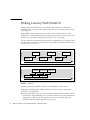
Hiding Latency With Prefetch
Fetching data from main memory is generally costly. Prefetch is an interesting
technique used to avoid or reduce the time the processor is waiting for data to arrive
in the registers.
With prefetch, data (or instructions) is moved closer to the CPU prior to usage.
Hopefully, it is then available by the time the processor needs it. Even if it has not
arrived yet, it will help in reducing the processor wait, or stall, time.
FIGURE 4 shows this graphically. Note that this is a simplification, as it suggests that
the time spent in the processor equals that of the memory reference time. This need
not be the case, of course.
Typical execution pattern without prefetch
Processor
Activity
Processor
Memory
Memory
Processor
Memory
Execution time
Activity
Typical execution pattern with prefetch
Processor
Processor
Memory
Memory
Memory
Processor
Execution time
FIGURE 4
Prefetch
Thanks to prefetch, the memory latency can be hidden to a certain extent.
Although conceptually quite simple, prefetch is not always easy to implement
efficiently in an application:
■
8
To hide the latency, the processor must perform sufficient other activities to allow
time for the actual prefetching to occur. These activities may not be present in the
application, or there are not enough other resources (for example, registers)
available while the prefetch operation is in progress.
Memory Hierarchy in Cache-based Systems • November 2002
■
Predicting where in the memory hierarchy the data resides is difficult. Usually the
location of the data is not constant while an application is executing. The question
is then where to prefetch from as the location in the memory hierarchy dictates
the time required for the prefetch to occur.
Prefetch is an instruction that initiates the movement of data from memory towards
the processor. There are several key aspects to consider when using prefetch:
■
Selecting which accesses are likely to miss in the cache and so should/could use
prefetch.
■
Selecting where to place the prefetch instruction (prefetch must be executed
sufficiently early).
■
Knowing the memory address for use in the inserted prefetch instruction.
Despite these potential drawbacks, prefetch is a powerful technique to improve
application performance, and is worth considering as part of tuning the performance
of an application.
Cache Organization and Replacement
Policies
Caches have a certain organization and a replacement policy. The organization
describes in what way the lines are organized within the cache. The replacement
policy dictates which line will be removed (evicted) from the cache in case an
incoming line must be placed in the cache.
Direct Mapped
Direct mapped is a simple and efficient organization. The (virtual or physical)
memory address of the incoming cache line controls which cache location is going to
be used.
Implementing this organization is straightforward and is relatively easy to make it
scale with the processor clock.
In a direct mapped organization, the replacement policy is built-in because cache
line replacement is controlled by the (virtual or physical) memory address.
In many cases this design works well, but, because the candidate location is
controlled by the memory address and not the usage, this policy has the potential
downside of replacing a cache line that still contains information needed shortly
afterwards.
Cache Organization and Replacement Policies
9
Any line with the same address modulo the cache size, will map onto the same cache
location. As long as the program accesses one single stream of data consecutively
(unit stride) all is well. If the program skips elements or accesses multiple data
streams simultaneously, additional cache refills may be generated.
Consider a simple example—a 4-kilobyte cache with a line size of 32 bytes directmapped on virtual addresses. Thus each load/store to cache moves 32 bytes. If one
variable of type float takes 4 bytes on our system, each cache line will hold eight
(32/4=8) such variables.
The following loop calculates the inner product of these two arrays. Each array
element is assumed to be 4 bytes long; the data has not been cached yet.
float a[1024], b[1024];
for (i=0; i<1024; i++)
sum += a[i]*b[i];
The generic system executes this loop as follows:
i
Operation Status In cache
Comment
0
load a[0] miss
load b[0] miss
t=a[0]*b[0]
sum += t
load a[1] hit
load b[1] hit
t=a[1]*b[1]
sum += t
..... etc .....
load a[7] hit
load b[7] hit
t=a[7]*b[7]
sum += t
load a[8] miss
load b[8] miss
t=a[8]*b[8]
sum += t
load a[9] hit
load b[9] hit
t=a[9]*b[9]
sum += t
.......
a[0..7]
b[0..7]
assume a[] was not cached yet
assume b[] was not cached yet
a[0..7]
b[0..7]
previous load brought it in
previous load brought it in
1
7
8
9
10
a[0..7]
b[0..7]
previous load brought it in
previous load brought it in
a[8..15] this line was not cached yet
b[8..15] this line was not cached yet
a[8..15] previous load brought it in
b[8..15] previous load brought it in
Memory Hierarchy in Cache-based Systems • November 2002
In this example a[0...7] denotes elements a[0],..,a[7] ; a similar notation is used for
vector b and other array squences of elements.
The cache hit rate is 7/8, which equals 87.5 percent. However, this is the best case
scenario.
Assume that the two arrays a[1024] and b[1024] are stored consecutively in memory.
That is, a[i+1] follows a[i] (i=0.,,,.n-2) in memory and b[0] follows a[n-1], b[1] again
follows b[0], and so forth. This loop will no longer perform as nicely as indicated
previously.
In this case, the following occurs:
i
Operation Status In cache Comment
0
load a[0] miss
load b[0] miss
1
2
t=a[0]*b[0]
sum += t
load a[1] miss
load b[1] miss
t=a[1]*b[1]
sum += t
load a[2] miss
load b[2] miss
.......
a[0..7]
b[0..7]
assume a[] was not cached yet
b[0] is 4 KByte away from a[0] in
memory and will wipe out
a[0..7] from the cache
a[0..7]
b[0..7]
previous load wiped out a[0..7]
previous load wiped out b[0..7]
a[0..7]
b[0..7]
previous load wiped out a[0..7]
previous load wiped out b[0..7]
Because of the direct-mapped architecture of the cache and the way the data is
organized, every array reference results in a cache miss. This degrades performance
noticeably. More specifically, you get seven times as many cache misses as in the
favorable scenario. This is called cache thrashing.
Several software-based solutions to this thrashing problem are available. At the
source code level, you might consider unrolling the loop. In the following example
this has been done to a depth of two.
for (i=0; i<1024; i+=2){
ta0 = a[i];
ta1 = a[i+1];
tb0 = b[i];
tb1 = b[i+1];
sum += ta0*tb0+ta1*tb1;
}
Cache Organization and Replacement Policies
11
The advantage of this approach is that now a[i+1] and b[i+1] are used before the
cache line they are part of is evicted from the cache. Note that the optimal unroll
depth is eight so all elements brought in are used immediately, before they are
evicted by a next load.
The downside of loop unrolling is the need for more registers. For example, the
original loop needs three floating point registers to store a[i], b[i] and sum. The
unrolled version needs five floating point registers.
On Sun systems with direct mapped caches, several solutions are available. At a
higher level, you might get help from the Solaris OE and/or compiler.
Because the mapping is a function of the memory address, the Solaris OE might
change the addresses such that different lines no longer map onto the same cache
location. This technique is often referred to as page coloring or cache coloring
(MauMcDl).
The compiler typically unrolls loops and supports padding of data5 to avoid
collisions.
Fully Associative
The fully associative cache design solves the potential problem of thrashing with a
direct-mapped cache. The replacement policy is no longer a function of the memory
address, but considers usage instead.
With this design, typically the oldest cache line is evicted from the cache. This policy
is called least recently used (LRU)6 .
In the previous example, LRU prevents the cache lines of a and b from being moved
out prematurely.
The downside of a fully associative design is cost. Additional logic is required to
track usage of lines. The larger the cache, the higher the cost. Therefore, it is difficult
to scale this technology to very large (data) caches. Luckily, a good alternative exists.
5. With padding, the addresses of the data are chosen such that thrashing is reduced or even avoided.
6. Other replacement policies (pseudo-LRU, LFU, FIFO, and so forth) are also possible.
12
Memory Hierarchy in Cache-based Systems • November 2002
Set Associative
A set-associative cache design uses several direct-mapped caches. Each cache is often
referred to as a set. On an incoming request, the cache controller decides which set
the line will go into. Within the set, a direct-mapped scheme is used to allocate a slot
in the cache.
The name reflects the number of direct-mapped caches. For example, in a 2-way set
associative design two direct mapped caches are used.
Another design parameter is the algorithm that selects the set. This could be
random, LRU, or any other selection scheme.
FIGURE 5 shows a four-way set associative cache.
Direct mapped
Cache
controller
Set 1
FIGURE 5
Set 2
Set 3
4-way set
associative
cache
Set 4
Four-Way Set Associative Design.
Note that a set-associative cache tends to reduce the amount of thrashing. Thrashing
can still occur, however, not only within one set but also between sets.
Thrashing between sets is a function of the algorithm that selects the set; whereas
thrashing within one set is related to the (virtual) memory address of the data.
Usually, the size of a set is 2n kilobytes (n=1, 2,...). If (virtual) addresses of incoming
lines in the same set are 2 m apart (m > n), thrashing occurs.
Cache Organization and Replacement Policies
13
For example, in a two-way set associative design, an update of this type might cause
thrashing:
float x[4096][4096];
for (i=1; i<n-1; i++)
for (j=1; j<n-1; j++)
x[i][j] = x[i][j-1]+x[i][j+1]+x[i][j]+x[i-1][j]+x[i+1][j];
FIGURE 6 shows the computational grid on which these computations are performed.
Array element x[i][j] is located at the intersection of the horizontal line at i and the
vertical line at j.
Storage/cache lines
i-1
i
i+1
j-1
FIGURE 6
j
j+1
Computational Grid
For a fixed value of i, this loop updates one cache line (containing x[i][j]) and
references two other lines (containing x[i-1][j] and x[i+1][j]).
Assume that the two lines containing x[i][j] and x[i-1][j] are in a different set (to
avoid collisions). The question is where the line with x[i+1][j] will go.
As there are only two sets, the cache controller has no other choice than to select a
set that already has one of the other two cache lines. In virtual memory, these three
lines are 4 * 4096 =16 kilobytes apart. Therefore, cache thrashing within one of the
sets will occur if one set is 16 kilobytes or less in size.
14
Memory Hierarchy in Cache-based Systems • November 2002
UltraSPARC III Cu Memory Hierarchy
TABLE 1 presents the memory hierarchy of the UltraSPARC™ III Cu microprocessor.
For more details, refer to [ArchManual].
TABLE 1
Cache Characteristics of the UltraSPARC III Cu Microprocessor
4Line
size
6Sub-
Cache
Function
Size
I-cache
Instructions
32 Kbytes
32 bytes
none
4-way set
associative
D-cache
Data
64 Kbytes
32 bytes
none
4-way set
associative
I-TLB
Address
16 entries1
Fully
associative
Address
128 entries2
2-way set
associative
Address
16 entries1
Fully
associative
Address
512 entries1, 3
2-way set
associative
Address
512 entries1, 3
2-way set
associative
P-cache
Prefetch
2 Kbytes
64 bytes
32 bytes
4-way set
associative
W-cache
Stores
2 Kbytes
64 bytes
32 bytes
4-way set
associative
E-cache
Unified
8 Mbytes
64-512 bytes 5
64 bytes
2-way set
associative
D-TLB
block
Organization
1. Can hold entries for 8-kilobyte, 64-kilobyte, 512-kilobyte, and 4-megabyte page sizes.
2. Used exclusively for 8-kilobyte pages.
3. At any one time this TLB is configured to only handle one of the page sizes.
4. Line size is not applicable to a TLB cache.
5. Line size depends on cache size.
6. Subblock is not applicable to a TLB cache.
As TABLE 1 shows, the UltraSPARC III Cu processor has two caches that have not yet
been mentioned.
UltraSPARC III Cu Memory Hierarchy
15
The P-cache is a prefetch cache, used to store data that has been brought in as a result
of a prefetch operation (instruction or hardware initiated, if supported). Only
floating point loads can get data from the P-cache.
The W-cache acts as a holding station for stored data. This cache reduces bandwidth
to the E-cache by coalescing and bursting stores to the E-cache.
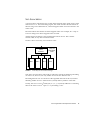
FIGURE 7 is a block diagram with the main components of the memory hierarchy on
the UltraSPARC III Cu microprocessor. The arrows indicate the various prefetch
possibilities. For more details, refer to [ArchManual].
As commented earlier, UltraSPARC has two separate TLBs for instruction and data
(I-TLB and D-TLB, respectively). In FIGURE 7, these TLBs are not shown as separate
blocks, but labelled TLBs instead.
Memory
f
SW
pre
E-cache
Register
file
W-cache
HW
+S
W
D-cache
TLBs
pre
f
P-cache
aS
ltr
U
I-cache
P
A
R
C
III
C
u
CPU
FIGURE 7
16
Main Components of the Memory Hierarchy
Memory Hierarchy in Cache-based Systems • November 2002
Performance Aspects
This section uses a simple example to demonstrate the way the memory hierarchy
should be used and how performance can degrade if data is not accessed in the
intended way.
Consider the following loop that sums up all elements in a two-dimensional array.
float x[m][n];
for (i=0; i<m; i++)
for (j=0; j<n; j++)
.......... (1)
sum += x[i][j];
To simplify the discussion, assume the following:
■
Matrix x, or a subset, is not present yet in any of the caches in the system
■
The first element x[0][0] is at a data cache line boundary and the first element in a
virtual memory page
■
The dimensions of x are a multiple of four—such that four rows span one virtual
memory page
■
The system has only one data cache.
■
A data cache line contains four elements
None of these assumptions are crucial in the remainder of the discussion. They
simply make the explanation a little easier.
FIGURE 8 uses shading to indicate in what way the matrix is built up, as seen from a
memory access and storage perspective. In this figure, the matrix fits in two pages.
Each row consists of four data cache lines.
UltraSPARC III Cu Memory Hierarchy
17
0
1
2
3
4
.
.
.
.
.
.
.
.
.
.
.
.
.
n-1
Virtual memory
page
0
Cache line
1
2
.
.
.
.
.
m-1
Virtual memory page
Virtual memory page
Data cache line
Data cache miss
TLB and data cache miss
FIGURE 8
Matrix x
The nested loop in (1) is ordered such that element x[0][0] is the first one to be read.
Because (by assumption) none of the data is cached anywhere, this memory access
results in both a data cache miss and a TLB miss. The latter is because the page that
this element is part of has not been mapped in the TLB cache yet. Therefore, this is a
very expensive reference.
The next reference is to x[0][1]. This element is included in the cache line that was
brought in as a result of the reference to x[0][0]. It is also part of the page that was
just mapped into the TLB. As a result, this is a very fast memory access. Elements
x[0][2] and x[0][3] will have similar fast memory access.
However, the reference to x[0][4] will be slower, because a new cache line must be
brought in. Reading x[0][5] will be fast again, because it is part of the second cache
line that was just loaded into the data cache.
This pattern repeats itself until all the elements in the first page are exhausted. In the
example, the last element is x[3][n-1].
The reference to x[4][0] results in both a data cache and a TLB miss again. The TLB
miss is because this element is part of the second page and no data in this page has
been accessed yet.
18
Memory Hierarchy in Cache-based Systems • November 2002
It is easy to see that this kind of memory access pattern produces (m* n)/4 data cache
misses and m/4 TLB misses.
Other than potentially reusing previously cached elements, little can be done to
avoid these transfers (referred to as the natural cache traffic).
The preceding example demonstrates what happens if memory access follows the
storage order. The following paragraphs discuss what happens if such a favorable
memory access pattern does not exist. The same nested loop is discussed, but with
the order of the loops interchanged:
float x[m][n];
for (j=0; j<n; j++)
for (i=0; i<m; i++)
.......... (2)
sum += x[i][j];
Similar to the previous example, the first reference (to x[0][0]) results in a data cache
and TLB miss.
The next reference is to x[1][0]. This element is still part of the same page (and hence
no TLB miss occurs), but not part of the cache line just brought in. Therefore, this
reference results a data cache miss. Likewise, the references to x[2][0] and x[3][0]
each results in a data cache miss.
On the next reference, to x[4][0], a TLB miss occurs because a page boundary is being
crossed. The references to x[5][0], x[6][0] and x[7][0] cause a data cache line miss
again.
While progressing through the first column of the matrix, the TLB and data cache are
filled up. What happens next depends on the value of m.
If m is sufficiently small, the cache lines and TLB entries are still present when
proceeding to the next column (j=1 in the loop above). If this is the case, all is well.
TLB entries are no longer needed and the values of x[0..m-1][1] are all in the data
cache already. If a cache line spans four elements, references to x[0..m-1][4] again
result in cache misses, but these misses are part of the natural traffic between main
memory and the cache subsystem.
Performance problems arise if m and n are large. To make this more specific, an
imaginary system with the following memory characteristics is introduced7:
A data cache with a capacity of 32 kilobytes, LRU replacement, and a line size of 16
bytes
■
A fully associative TLB with 256 entries
■
One virtual memory page has a size of 4 kilobytes
7. This is not what is used on Sun systems and only chosen for purpose of this example.
UltraSPARC III Cu Memory Hierarchy
19
One cache line contains 16/4 = 4 elements8. The system can store 32 Kbytes/16 = 2048
cache lines in the data cache and map 256*4 = 1 megabyte of data in the TLB. If the
data requirement exceeds one or both of these thresholds, performance degrades.
Assume that m = 4096 and n = 1024.
By the time 2048 elements of the first column of matrix x are read, the data cache is
full. It contains the first four columns of the matrix.
The next reference (i=2048), causes one of the lines to be removed from the cache
(evicted). Because of the LRU replacement, the very first cache line loaded
(x[0][0]...x[0][3]) is evicted from the cache.
For i = 2049, the second cache line will be replaced, and so forth.
After the last value of the inner loop iteration (i=4095) is executed, the top half of the
first four columns of matrix x are replaced by the bottom part of the first four
columns.
TABLE 2 shows a snapshot of the data cache after it has finished processing the
iteration for the indicated values of j and i.
TABLE 2
Three Snapshots of the Data Cache
J=0 I=2047
x[
x[
x[
x[
0]
1]
2]
3]
[0]
[0]
[0]
[0]
...
...
...
...
x[
x[
x[
x[
0]
1]
2]
3]
[3]
[3]
[3]
[3]
J=0 I=2048
x[
x[
x[
x[
2048]
1] [0]
2] [0]
3] [0]
[0] ... x[ 2048] [3]
... x[ 1] [3]
... x[ 2] [3]
... x[ 3] [3]
J=0 I=4095
x[2048]
x[2049]
x[2050]
x[2051]
[0]
[0]
[0]
[0]
...
...
...
...
x[2048]
x[2049]
x[2050]
x[2051]
[3]
[3]
[3]
[3]
...
...
...
x[2046] [0] ... x[2046] [3]
x[2047] [0] ... x[2047] [3]
x[2046] [0] ... x[2046] [3]
x[2047] [0] ... x[2047] [3]
x[4094][0] ... x[4094][3]
x[4095][0] ... x[4095][3]
When the program processes the next column of the matrix, j=1, all cache lines must
be reloaded again. For example, the first element needed is x[0][1]. Initially this was
brought into the cache for j = 0 and i = 0, but it was evicted when loading
subsequent elements of the matrix.
Therefore, all references to the second column of the matrix result in a cache miss
again. There is no spatial locality (that is, not using all of the elements in one cache
line.) In a similar manner, it can be seen that all references to the subsequent
columns of the matrix are cache misses.
In other words, all references to x[i][j] result in a cache miss. As a result,
performance is very poor.
8. We assume that a variable of type float is stored in four bytes.
20
Memory Hierarchy in Cache-based Systems • November 2002
But, things are even worse than this. Due to the poor memory access pattern, no
spatial or temporal locality (that is re-use of cache lines) is obtained in the TLB cache
either. Every reference to a matrix element results in a TLB miss too.
The explanation for this is similar to that seen for the data cache.
The TLB cache has a capacity of 256 entries. One row of the matrix is 1024 * 4 = 4
kilobytes, which is exactly the size of one virtual memory page.
The program starts reading the first column of the matrix (j = 0). A TLB entry must
be set up for the page that contains x[0][0]. The next reference is to x[1][0]. This
element has not yet been mapped into the TLB either, giving rise to another TLB
miss. This pattern is repeated for the next 254 iterations: they all cause a TLB entry to
be set up.
When i = 256 an older entry must be replaced instead of re-using these cached
entries because the TLB cache is full. Similar to what was seen with the data cache,
subsequent loop iterations evict older entries from the TLB. For i = 511, all first 256
entries have been flushed out of the TLB.
By the time the program processes all elements in the first column of matrix, the TLB
entries map to the last 256 rows of the matrix.
Unfortunately, the program cannot access these elements, but starts with the top part
of the matrix again. None of the pages corresponding to these elements are in the
TLB and a TLB miss occurs again on every matrix reference.
This pattern repeats itself over and over again, resulting in a TLB miss on every
reference to matrix x.
It is clear that this loop performs very poorly under these circumstances.
For larger matrixes, the behavior is similar. If the values for m and/or n are reduced,
some or all of these effects are less pronounced. For small matrixes, they will be gone
entirely.
Performance Results
To illustrate the preceding data, this example was run on a UltraSPARC III Cu
processor at 900 Mhz in a Sun Fire™ 6800 system.
In the row-oriented version, the inner loop is over the rows of the matrix:
for (i=0; i<m; i++)
for (j=0; j<n; j++)
sum += x[i][j];
UltraSPARC III Cu Memory Hierarchy
21
In the column-oriented version, the inner loop is over the columns of the matrix:
for (j=0; j<n; j++)
for (i=0; i<m; i++)
sum += x[i][j];
Without special precautions, the C compiler from the Sun ONE™ Studio 7 Compiler
Collection suite transforms the column version with the bad memory access pattern
into the row version. This is, of course, the right thing to do, but it defeats the
purpose of our experiment. To prevent this optimization, we crafted the example to
prevent the compiler from applying the loop interchange.
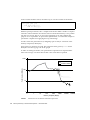
FIGURE 9 shows the performances (in Megaflops per second) as a function of the
memory footprint (in kilobytes).
Only square nxn matrices are used. The footprint is then given by n * n * 4/1024
kilobytes. Note the log-log scale in the graph.
To filter out timing anomalies, each performance experiment was repeated three
times. The average over these three results is the value that was plotted.
1000
Performance (Mflop/s)
Row version
Column version
100
10
1
0
1
10
100
1000
10000
Memory Footprint (KByte)
FIGURE 9
22
Performance of the Matrix Summation Operation
Memory Hierarchy in Cache-based Systems • November 2002
100000
100000
The shape of these curves is not surprising. With both versions, the performance is
highest for a footprint of about 64 kilobytes, the size of the L1 D-cache on the
UltraSPARC III Cu processor.
Because the entire matrix fits in this cache, it will also fit in the D-TLB cache and the
memory access pattern is irrelevant when it comes to performance.
However, there is a slight difference between the two versions. The column-oriented
version is slightly slower. Additional cache conflicts cause this difference. The
column version has a non-unit stride access pattern, increasing the chance of
premature cache line evictions.
In general, the curve for the row version is smoother than for the column version.
This is because the non-unit stride access pattern in the latter gives rise to more
cache line collisions.
Once the matrix no longer fits in the D-cache but still fits in the L2 E-cache,
performance degrades, but the performance curves are still similar. This is because
all of the matrix can be mapped into the E-cache and D-TLB.
As soon as the matrix no longer fits in the E-cache, performance degrades again, but
the curves are no longer identical. The row version outperforms the column version
in a rather dramatic way. It is about four to five times faster.
Software Prefetch Effect
Studying the effect of software prefetch is interesting. The previous results shown
were obtained with software prefetch disabled (-xprefetch=no compiler option).
With the -xprefetch=yes option, the compiler applies heuristics to decide which
prefetch instructions to insert and whether or not to insert them.
On small problems, prefetching data is not meaningful, as the matrix will be in one
of the caches anyway. There is not much latency to hide and the additional cost of
the prefetch instruction only slows down the program.
A prefetch instruction on data that is not mapped into the D-TLB will be dropped.
The poor memory access pattern in the column version generates many D-TLB
misses on large matrices. Therefore, there is no practical reason to insert prefetch
instructions in the column version. 9
9. Through an optimization technique called loop-blocking this problem can be circumvented. Using large
pages also helps. Both topics are beyond the scope of this article.
UltraSPARC III Cu Memory Hierarchy
23
This is different for the row version. Thanks to the favorable memory access pattern,
this algorithm only generates a modest amount of D-TLB misses compared to the
total number of cache references. When accessing a large matrix, prefetch should,
therefore, help hide the memory latency
FIGURE 10 is a plot of the performance for the row version, with and without
software prefetch. The speed-up (performance ratio between the two versions) is
given in FIGURE 11.
Comparing the performances shown in FIGURE 9 and FIGURE 10, it is seen that
prefetch not only improves performance for large matrices that do not fit in the level
2 E-cache, but also helps for data sets that are E-cache resident. For a memory
footprint between 64 kilobytes and 8 megabytes, the row version with prefetch does
not degrade in performance (FIGURE 10), whereas the original version without
prefetch does (FIGURE 9).
1000
Performance (Mflop/s)
Row version
Row version with
prefetch
100
10
0
FIGURE 10
1
10
100
1000
10000
Memory Footprint (KByte)
100000
1000000
Effect of Software Prefetch on the Row Oriented Version.
For matrices that fit in the D-cache, prefetch slows down the operation, but the
degradation is limited to approximately 20 percent.
For larger matrices, prefetch has a significant effect on performance. The speed-up
for E-cache resident matrices is close to 4. For larger matrices, the speed-up is more
than a factor of 5.
24
Memory Hierarchy in Cache-based Systems • November 2002
5.5
5.0
4.5
4.0
3.5
3.0
2.5
2.0
1.5
1.0
0.5
0
1
10
100
1000
10000
100000
10000
Memory Footprint (KByte)
FIGURE 11
Performance Ratio for the Row Version With and Without Prefetch.
References
Adrian Cockcroft, Richard Pettit, Sun Performance and Tuning (Java and the Internet),
Sun Microsystems Press, ISBN 0-13-095249-4, 1998.
[Handy]
Jim Handy, The Cache Memory Book, Morgan Kaufmann Publishers, ISBN
0123229804, 1997.
[MauMcDl]
Jim Mauro, Richard McDougall Solaris Internals (Core Kernel Architecture), Sun
Microsystems Press, ISBN 0-13-022496-0, 2001.
[ArchManual] UltraSPARC III Cu User's Manual, Version V1.0, May 2002, Sun Microsystems
(http://www.sun.com/processors/manuals/index.html)
[CocPet]
References
25
About the Author
Ruud van der Pas studied numerical mathematics and physics at the University of
Utrecht in The Netherlands. He has been involved with high performance
computing since 1985 and joined Sun Microsystems in 1998. The focus of his work
has always been on the performance of technical scientific applications and the
underlying architecture. He has a wealth of practical experience on a variety of
systems, ranging from vector computers, SMP systems, distributed memory
computers to Cache Coherent Non-Uniform Memory Access (cc-NUMA)
architectures.
Ruud’s expertise is in serial performance and shared memory parallelization. He is
not only actively involved in porting and tuning user applications, but consultants
on these topics with customers too. Additionally, he regularly gives technical
presentations and workshops at conferences and seminars.
Ordering Sun Documents
The SunDocs SM program provides more than 250 manuals from Sun Microsystems,
Inc. If you live in the United States, Canada, Europe, or Japan, you can purchase
documentation sets or individual manuals through this program.
Accessing Sun Documentation Online
The docs.sun.com web site enables you to access Sun technical documentation
online. You can browse the docs.sun.com archive or search for a specific book title
or subject. The URL is http://docs.sun.com/
To reference Sun BluePrints OnLine articles, visit the Sun BluePrints™ OnLine Web
site at: http://www.sun.com/blueprints/online.html
26
Memory Hierarchy in Cache-based Systems • November 2002