1
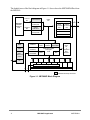
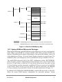
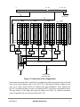
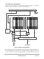
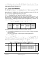
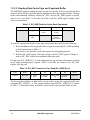
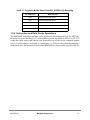
5/99
MPC860P
Supplement to the MPC860 PowerQUICC™ User’s Manual
© Motorola Inc. 1999. All rights reserved.
This document contains information on a new product under development. Motorola reserves the right to change or discontinue this product without notice. Information in this document is provided solely to enable system and software implementers to use PowerPC microprocessors. There are no express or implied copyright licenses granted hereunder to design or fabricate PowerPC integrated circuits or integrated circuits based on the information in this document.
Motorola reserves the right to make changes without further notice to any products herein. Motorola makes no warranty, representation or guarantee regarding the
suitability of its products for any particular purpose, nor does Motorola assume any liability arising out of the application or use of any product or circuit, and
specifically disclaims any and all liability, including without limitation consequential or incidental damages. “Typical” parameters can and do vary in different
applications. All operating parameters, including “Typicals” must be validated for each customer application by customer’s technical experts. Motorola does not
convey any license under its patent rights nor the rights of others. Motorola products are not designed, intended, or authorized for use as components in systems
intended for surgical implant into the body, or other applications intended to support or sustain life, or for any other application in which the failure of the Motorola
product could create a situation where personal injury or death may occur. Should Buyer purchase or use Motorola products for any such unintended or
unauthorized application, Buyer shall indemnify and hold Motorola and its officers, employees, subsidiaries, affiliates, and distributors harmless against all claims,
costs, damages, and expenses, and reasonable attorney fees arising out of, directly or indirectly, any claim of personal injury or death associated with such
unintended or unauthorized use, even if such claim alleges that Motorola was negligent regarding the design or manufacture of the part.
Motorola and
are registered trademarks of Motorola, Inc. Motorola, Inc. is an Equal Opportunity/Affirmative Action Employer.
10
10
This supplement to the MPC860 PowerQUICC™ User’s Manual highlights
implementation-specific features of the MPC860 Plus (MPC860P) and how they differ
from the MPC860. For features not described in this document, consult the MPC860
PowerQUICC™ User’s Manual, the MPC8xx ATM Supplement to the MPC860/MPC850
PowerQUICC ™ User’s Manual, the MPC860T Fast Ethernet Controller Supplement to
the MPC860 PowerQUICC™ User’s Manual, and the QUICC ™ Multichannel Controller
Supplement to the MC68360 & MPC860 User’s Manual.
To locate any published errata or updates for this document, refer to the website at
http://www.mot.com/netcomm.
1.1 Overview of the MPC860P
The MPC860P is a pin-compatible enhanced version of the MPC860 PowerQUICC™
microprocessor that increases the instruction cache size from 4 to 16 Kbytes and the data
cache from 4 to 8 Kbytes. Dual-port RAM is increased from 5 to 8 Kbytes, extending the
flexibility and capabilities of the communications processor module (CPM). The MPC860P
is also capable of system clock rates of 80 MHz and faster.
As a superset of the MPC860SR and the MPC860T (revision D), the MPC860P supports
ATM features including the UTOPIA interface, 10/100 base-T (Fast) Ethernet, and QMC
microcode for multichannel HDLC support.
Features of the MPC860P not implemented in the MPC860 are as follows:
•
•
•
•
•
Larger 8-Kbyte dual-port RAM, see Section 1.2, “Dual-Port RAM.”
Improvements to cache implementation, see Section 1.3, “Instruction and Data
Caches.”
— 16-Kbyte, 4-way set-associative instruction cache
— 8-Kbyte, 2-way set-associative data cache
ATM support, see the MPC8xx ATM Supplement to the MPC860/MPC850
PowerQUICC ™ User’s Manual
Fast Ethernet support, see the MPC860T Fast Ethernet Controller Supplement to the
MPC860 PowerQUICC™ User’s Manual
Multichannel HDLC support, see the QUICC ™ Multichannel Controller
Supplement to the MC68360 & MPC860 User’s Manual
MOTOROLA
MPC860P Supplement
-1
The shaded areas of the block diagram in Figure 1-1 show where the MPC860P differs from
the MPC860.
Instruction
Bus
Embedded
PowerPC
Processor
Core
16-Kbyte
Instruction Cache
System Interface Unit (SIU)
Unified
Bus
Memory Controller
Instruction MMU
32-Entry ITLB
Load/Store
Bus
Internal
External
Bus Interface Bus Interface
Unit
Unit
8-Kbyte
Data Cache
System Functions
Data MMU
32-Entry DTLB
Real-Time Clock
PCMCIA-ATA Interface
DMAs
Parallel I/O
FIFOs
4 Baud Rate
Generators
10/100
Base-T
Media Access
Control
4
Timers
Parallel Interface Port
Timers
and UTOPIA
Interrupt
8-Kbyte
Controllers Dual-Port RAM
32-Bit RISC Controller
and Program
ROM
MAC
16 Virtual
Serial
and
2
Independent
DMA
Channels
MII
SCC1
SCC2
SCC3
SCC4
SMC1
SMC2
SPI
I2C
Time Slot Assigner
Serial Interface
Shaded blocks identify new features.
Figure 1-1. MPC860P Block Diagram
-2
MPC860P Supplement
MOTOROLA
1.2 Dual-Port RAM
This section describes how the MPC860P implements the 8-Kbyte dual-port RAM.
Chapter 18, “Communications Processor,” of the MPC860 PowerQUICC™ User’s Manual
has a complete description of the dual-port RAM.
1.2.1 RISC Microcode Development Support Control Register
(RMDS)
To accommodate the larger dual-port RAM, the MPC860P has an additional control
register called the RISC microcode development support control register (RMDS). It is
located near the RISC controller configuration register (RCCR) in the CP area of the
internal memory map; see Table 1-1. (The RMDS area is reserved in the MPC860.)
Table 1-1. RMDS Location in the CP Area of the Internal Memory Map
Communications Processor (CP)
Offset
Name
Size
0x9C0
CPCR—CP command register
16 bits
0x9C2–0x9C3
Reserved
2 bytes
0x9C4
RCCR—RISC controller configuration register
16 bits
0x9C6
Reserved
8 bits
0x9C7
RMDS—RISC microcode development support control register
8 bits
.
.
.
.
.
.
.
.
.
RMDS, shown in Figure 1-2, determines which regions of the dual-port RAM can contain
executable microcode. RMDS is used with RCCR[ERAM] to determine the valid address
space for executable microcode. Section 1.2.3, “System RAM and Microcode Packages,”
describes the partitioning of the dual-port system RAM.
Bit
0
Field
ERAM4K
1
2
3
4
5
6
7
—
Reset
0000_0000_0000_0000
R/W
R/W
Addr
0x9C7
Figure 1-2. RISC Microcode Development Support Control Register (RMDS)
RMDS fields are described in Table 1-2.
MOTOROLA
MPC860P Supplement
-3
Table 1-2. RMDS Field Descriptions
Bits
Name
0
ERAM4K
1–7
—
Description
Enable RAM microcode (at offset 4K)
0 Microcode may be executed only from the first 2 Kbytes of the dual-port RAM.
1 Microcode is also executed from the 2 Kbytes of the second half of the dual-port RAM with a
512-byte extension.
Reserved, should be cleared.
1.2.2 Dual-Port RAM Map
The CPM of the MPC860P has 8 Kbytes of static RAM configured as dual-port memory,
shown in Figure 1-3.
Dual-Port RAM
1,024 Bytes
BD/Buffers/Microcode
1,024 Bytes
BD/Buffers/Microcode
U-Bus Addr
CP Microcode Instr Addr
512 Bytes
BD/Buffers/Microcode
Address
Selectors
CP Data Addr
1,024 Bytes
BD/Buffers/Microcode
Data
Selectors
CP Microcode Instr
U-Bus Data
CP Data
1,024 Bytes
BD/Buffers/Microcode
512 Bytes
BD/Buffers/Microcode
2,048 Bytes
BD/Buffers
U-Bus Addr
Address
Selectors
CP Data Addr
1,024 Bytes
Parameter RAM
Data
Selectors
Shaded area is system RAM. Note that in this figure, the area is not contiguous memory. For an accurate
representation of the physical implementation, see Figure 1-4.
Figure 1-3. Dual-Port RAM Block Diagram
The dual-port RAM consists of 7 Kbytes of system RAM (see Section 1.2.3, “System RAM
and Microcode Packages”) and 1 Kbyte of parameter RAM.
The controller and sub-block parameters of the parameter RAM and the optional microcode
packages in system RAM use fixed addresses. The buffer descriptors, buffers, and scratch
pad area, however, can be located in any unused dual-port RAM area. See Figure 1-4.
-4
MPC860P Supplement
MOTOROLA
0 Kbyte–
ERAM = 01–
ERAM = 10–
BD/Data/Microcode IMMR + 0x2000
BD/Data/Microcode IMMR + 0x2200
ERAM = 11–
1 Kbyte–
IMMR + 0x2400
BD/Data/Microcode
2 Kbyte–
IMMR + 0x2800
BD/Data
3 Kbyte–
ERAM = 11–
ERAM = 01, 10–
ERAM4K = 1–
BD/Data/Microcode IMMR + 0x2E00
IMMR + 0x2F00
IMMR + 0x3000
4 Kbyte–
5 Kbyte– BD/Data/Microcode
6 Kbyte–
BD/Data
IMMR + 0x3800
BD/Data/Microcode IMMR + 0x3A00
ERAM4K = 1–
7 Kbyte–
Parameters for the
Peripheral Controllers
Parameter RAM–
IMMR + 0x3C00
8 Kbyte–
RCCR[ERAM] governs memory allocation for microcode in dark-shaded areas.
RMDS[ERAM4K] governs memory allocation for microcode in light-shaded areas.
Figure 1-4. Dual-Port RAM Memory Map
1.2.3 System RAM and Microcode Packages
When optional Motorola-supplied RAM microcode packages are activated, certain portions
of the 7-Kbyte system RAM are no longer available. (The 1-Kbyte parameter RAM is not
affected.) Depending on the memory requirements of the microcode package, some or all
of the shaded areas of Figure 1-4 become locked. Reads to locked areas return all ones. The
unshaded 2-Kbyte (non-contiguous) area of system RAM is always available to the user.
The enable-RAM-microcode field of the RISC configuration register, RCCR[ERAM],
selects the three possible configurations for microcode area sizes—first 512-byte block,
first two 512-byte blocks, or first four 512-byte blocks. When just the first and/or second
512-byte blocks are used for microcode, an additional 256-byte extension of system RAM
is also locked. When all four 512-byte blocks are used for microcode, an additional
512-byte extension of system RAM is locked. See the dark-shaded areas of Figure 1-4.
In addition to RCCR[ERAM], RMDS[ERAM4K] (enable RAM microcode at offset 4K)
affects the system RAM memory configuration for microcode packages. Setting
MOTOROLA
MPC860P Supplement
-5
RMDS[ERAM4K] locks a 2-Kbyte block and a 512-byte extension (the light-shaded areas
of Figure 1-4) for microcode execution.
1.3 Instruction and Data Caches
This section describes the MPC860P differences in the organization of the on-chip
instruction and data caches, and in the bit fields of the cache control registers. See the cache
chapter of the MPC860 PowerQUICC™ User’s Manual for a complete description.
The MPC860P cache implementation has the following enhancements:
•
•
The instruction cache is 16 Kbytes. It has 256 sets and is four-way set associative.
The data cache is 8 Kbytes. It has 256 sets and is two-way set associative.
1.3.1 Instruction Cache Organization
The MPC860P instruction cache is organized as 256 sets of four blocks, as shown in
Figure 1-5. Each block consists of 16 bytes, a single state bit, a lock bit, and an address tag.
-6
MPC860P Supplement
MOTOROLA
0
19
20
27 28
29
Instruction effective address
2
20
Word select
8
20
20
20
..
..
L
R
U
A
r
r
a
y
Valid bit
Lock bit
...
..
..
254
255
Way3
tag
0
1
w0
w1
w2
w3
..
..
Valid bit
Lock bit
...
..
..
. . 254
. . 255
set254 254
set255 255
Way2
tag
0
1
w0
w1
w2
w3
..
..
Valid bit
Lock bit
...
w0
w1
w2
w3
..
..
Valid bit
Lock bit
...
set0
set1
Way1
tag
0
1
w0
w1
w2
w3
Way0
tag
0
1
..
..
254
255
20
MMU
128
COMP
128
COMP
hit0
128
COMP
hit1
128
COMP
hit2
hit3
Bidirectional multiplexer 4 -> 1
128
HIT
To block buffer/
From burst buffer
Figure 1-5. Instruction Cache Organization
Each instruction cache block contains four contiguous words from memory that are loaded
from a four-word boundary; that is, bits A[28–31] of the logical (effective) addresses are
zero. As a result, cache blocks are aligned with page boundaries. Also, address bits
A[20–27] provide the index to select a set, and bits A[28–29] select a word within a block.
The tags consist of the high-order physical address bits PA[0–19]. Address translation
occurs in parallel with set selection (from A[20–27]).
MOTOROLA
MPC860P Supplement
-7
1.3.2 Data Cache Organization
The data cache is organized as 256 sets of two blocks as shown in Figure 1-6. Each block
consists of 16 bytes, two state bits, a lock bit, and an address tag.
0
19
20
27 28
31
Data effective address
4
20
Byte select
8
way0
set254 tag254
set255 tag255
tag0
tag1
w0 w1 w2 w3 . .
w0 w1 w2 w3 . .
..
..
tag254
tag255
20
...
...
...
w0 w1 w2 w3
w0 w1 w2 w3
Dirty bit
Valid bit
Lock bit
...
L
R
U
..
..
A
r
r
a
y
...
...
Dirty bit
Valid bit
Lock bit
...
tag0
tag1
...
set0
set1
way1
w0 w1 w2 w3 . .
w0 w1 w2 w3 . .
w0 w1 w2 w3
w0 w1 w2 w3
20
MMU
128
128
COMP
COMP
hit1
hit0
Bidirectional multiplexer 2 -> 1
128
HIT
To/from block buffer
To/from burst buffer
Figure 1-6. Data Cache Organization
Each cache block contains four contiguous words from memory that are loaded from a
four-word boundary; that is, bits A[28–31] of the logical (effective) addresses are zero. As
a result, cache blocks are aligned with page boundaries. Note that address bits A[20–27]
-8
MPC860P Supplement
MOTOROLA
provide the index to select a cache set. Bits A[28–31] select a byte within a block. The tags
consist of the high-order physical address bits PA[0–19]. Address translation occurs in
parallel with set selection (from A[20–27]).
1.3.3 Cache Control Registers
The MPC860P bit fields and commands of the cache control and status registers (IC_CST
and DC_CST) are unchanged from the MPC860; however, the bit fields of the cache
address registers (IC_ADR and DC_ADR) and the cache data port registers (IC_DAT and
DC_DAT) reflect the changed organization of the caches.
1.3.3.1 Reading Data and Tags in the Instruction Cache
The MPC860P supports reading the data, tags, and the state and lock bits stored in the
instruction cache. The instruction cache read command, issued by reading the IC_DAT
register, uses the IC_ADR register to qualify what is to be read. Table 1-3 describes the
fields of the IC_ADR register during an instruction cache read command.
Table 1-3. IC_ADR Fields for Cache Read Commands
0–16
Reserved
17
0 Tag
1 Data
18–19
00 Way 0
01 Way 1
10 Way 2
11 Way 3
20–27
28–29
30–31
Set select
(0–255)
Word select
(used only for
data array)
Reserved
To read the data or tags stored in the instruction cache, do the following:
1. Write the address of the data or tag to be read to the IC_ADR according to the format
shown in Table 1-3.
Note that it is also possible to read this register for debugging purposes.
2. Read the IC_DAT register.
For data array (IC_ADR[17] = 1) read commands, the word selected by IC_ADR[28–29]
is placed in the target general-purpose register. For tag array (IC_ADR[17] = 0) read
commands, the tag and state information is placed in the target general-purpose register.
Table 1-4 provides the format of the IC_DAT register for a tag read.
Table 1-4. IC_DAT Format for a Tag Read (IC_ADR[17] = 0)
0–19
20–21
22
Tag value
Reserved
0 Invalid
1 Valid
MOTOROLA
23
0 Unlocked
1 Locked
24–29
30–31
LRU code:
If bit 29 is set, way3 is more recent than way2.
If bit 28 is set, way3 is more recent than way1.
If bit 27 is set, way3 is more recent than way0.
If bit 26 is set, way2 is more recent than way1.
If bit 25 is set, way2 is more recent than way0.
If bit 24 is set, way1 is more recent than way0.
Reserved
MPC860P Supplement
-9
1.3.3.2 Reading Data Cache Tags and Copyback Buffer
The MPC860P supports reading the tags, the state bits and the lock bits stored in the data
cache as well as the last copyback address, and data words in the copyback buffer. The data
cache read command, issued by reading DC_DAT, uses the DC_ADR register to qualify
what is to be read. Table 1-5 describes the fields of the DC_ADR register during a data
cache read command.
Table 1-5. DC_ADR Fields for Cache Read Commands
0–17
Reserved
18
0 Tags
19
0 Way 0
1 Way 1
1 Copyback
buffer
Reserved
20–27
28–31
Set select
(0–255)
Reserved
Copyback buffer
address/
data-word select
To read the copyback buffer data or the tags stored in the data cache, do the following:
1. Write the address of the copyback buffer or tag to be read to the DC_ADR according
to the format shown in Table 1-5.
Note that it is also possible to read this register for debugging purposes.
2. Read the DC_DAT register. Note that writing to the DC_DAT register is illegal. A
write to DC_DAT results in an undefined data cache state.
For tag array (DC_ADR[18] = 0) read commands, the tag and state information is placed
in the target general-purpose register. Table 1-6 provides the format of the DC_DAT
register for a tag read.
Table 1-6. DC_DAT Format for a Tag Read (DC_ADR[18] = 0)
0–19
20–21
Tag value
Reserved
22
0 Invalid
1 Valid
23
0 Unlocked
1 Locked
24
25
LRU bit of this 0 Unmodified
set
1 Modified
26–31
Reserved
The last copyback address or data buffer can be read by using the copyback buffer read
command (DC_ADR[18] = 1). The copyback buffer select field (DC_ADR[20–27]), shown
in Table 1-7, determines which word of the cache block in the copyback buffer is read.
-10
MPC860P Supplement
MOTOROLA
Table 1-7. Copyback Buffer Select Field (DC_ADR[20–27]) Encoding
DC_ADR[20–27]
Buffer Selected
0x00
Copyback buffer data word 0
0x01
Copyback buffer data word 1
0x02
Copyback buffer data word 2
0x03
Copyback buffer data word 3
0x04
Copyback address
1.3.4 Instruction and Data Cache Operations
The MPC860P instruction and data cache operations are unchanged from the MPC860.
However, be aware that bits 20–27 of the address provide the index to select a set (0–255)
within the cache arrays, and that the tags from each way of the set are compared against
bits 0–19 of the address; see Figure 1-5 and Figure 1-6. Note also that when determining a
cache hit or miss, the instruction cache of the MPC860P has four possible ways for each set.
MOTOROLA
MPC860P Supplement
-11
-12
MPC860P Supplement
MOTOROLA