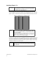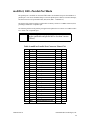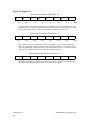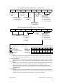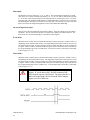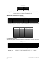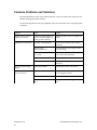
1
CME146786CX
cpuModuleTM User’s Manual
RTD Enhanced Award BIOS Versions 6.00.xx
ISO9001 and AS9100 Certified
BDM-610000068
Rev A
CME146786CX
cpuModuleTM
User’s Manual
RTD Embedded Technologies, Inc.
103 Innovation Blvd.
State College, PA 16803-0906
Phone: +1-814-234-8087
FAX: +1-814-234-5218
E-mail
[email protected]
[email protected]
web site
http://www.rtd.com
Revision History
Rev A
Initial Release
Published by:
RTD Embedded Technologies, Inc.
103 Innovation Blvd.
State College, PA 16803-0906
Copyright 1999, 2002-2009 by RTD Embedded Technologies, Inc.
All rights reserved
Printed in U.S.A.
The RTD Logo is a registered trademark of RTD Embedded Technologies. cpuModule and utilityModule
are trademarks of RTD Embedded Technologies. PS/2, PC/XT, PC/AT and IBM are trademarks of International Business Machines Inc. MS-DOS, Windows, Windows 95, Windows 98 and Windows NT are trademarks of Microsoft Corp. PC/104 is a registered trademark of PC/104 Consortium. All other trademarks
appearing in this document are the property of their respective owners.
Chapter 1: Introduction . . . . . . . . . . . . . . . . . . . . . . . . . . . . . . . . . . 3
The CME146786CX cpuModule ......................................................4
Specifications ....................................................................................6
Chapter 2: Getting Started . . . . . . . . . . . . . . . . . . . . . . . . . . . . . . . . 9
Basic Connector Locations ...............................................................10
Fail safe boot ROM ...........................................................................11
Cable Kits .........................................................................................12
Connecting Power .............................................................................13
Connecting the utility cable ..............................................................14
Connecting a Keyboard ....................................................................15
Connecting to the PC/104 Bus ..........................................................16
Booting the cpuModule for the First Time .......................................17
Booting to Boot Block Flash with Fail Safe Boot ROM ..................18
If You Misconfigure the cpuModule ................................................19
For More Information .......................................................................20
Chapter 3: Connecting the cpuModule . . . . . . . . . . . . . . . . . . . . . . 21
Connector Locations .........................................................................22
Auxiliary Power CN3 .......................................................................24
Serial Ports, CN7 and CN8 ...............................................................26
multiPort, CN6 - Parallel Port Mode ................................................29
multiPort, CN6 - aDIO Mode ...........................................................30
multiPort, CN6 - Floppy Controller Mode .......................................31
Multifunction Connector, CN5 .........................................................33
VGA Video Connector, CN18 ..........................................................35
EIDE Connector, CN9 ......................................................................36
ATA/IDE Disk Chip Socket, U8 ......................................................38
Bus Mouse Connector, CN4 .............................................................40
USB Connector,CN17 ......................................................................41
10/100 Base T and TX Connector, CN20 .........................................42
PC/104 Bus, CN1 and CN2 ..............................................................43
Chapter 4: Configuring the cpuModule (BIOS Setup) . . . . . . . . . 47
Disabling Fail Safe Boot ROM .........................................................48
Quick Boot Description ....................................................................49
Configuring with the RTD Enhanced Award BIOS .........................50
Chapter 5: Using the cpuModule . . . . . . . . . . . . . . . . . . . . . . . . . . . 51
Memory Map ....................................................................................52
Input/Output Address Map ...............................................................53
Hardware Interrupts ..........................................................................55
The RTD Enhanced Award BIOS ....................................................57
Thermal Throttling ............................................................................58
Direct Hardware Control ..................................................................59
Advanced Digital I/O Ports (aDIO) ..................................................60
Basic Interrupt Information for Programmers: .................................66
Watchdog Timer Control ..................................................................69
Multi-Color LED ..............................................................................72
Real Time Clock and CMOS Memory .............................................73
Parallel Port Control .........................................................................76
Storing Applications On-board .........................................................77
Configuring the ATA/IDE Disk Chip Socket ...................................78
Chapter 6: Hardware Reference . . . . . . . . . . . . . . . . . . . . . . . . . . . 79
Jumpers and Solder Jumper Settings ................................................80
Onboard PCI Devices .......................................................................84
Mechanical Dimensions ....................................................................85
Processor Thermal Management ......................................................86
Chapter 7: Troubleshooting . . . . . . . . . . . . . . . . . . . . . . . . . . . . . . . 87
Common Problems and Solutions .....................................................88
Troubleshooting a PC/104 System ...................................................91
How to Obtain Technical Support ....................................................92
Chapter 8: Limited Warranty . . . . . . . . . . . . . . . . . . . . . . . . . . . . . 93
Table Of Figures
CME146786CX Block Diagram .......................................................5
CME146786CX Basic Connector Locations ....................................10
CME146786CX Connector Locations ..............................................22
CME146786CX Jumper Locations - Top .........................................81
CME146786CX Jumper Locations - Bottom ...................................82
Table Of Tables
Power Consumption ..........................................................................8
CME146786CX Connectors .............................................................23
Auxiliary Power Connector CN3 ......................................................24
Serial Port Base Address and IRQ Options ......................................26
Serial Port in RS-232 Mode ..............................................................26
RS-422 Serial Port Connections .......................................................27
RS-485 Serial Port Connections .......................................................27
Serial Port in RS-422/485 Mode .......................................................28
multiPort Parallel Port Connector Pinout CN6 .................................29
multiPort Advanced Digital I/O Connector Pinout CN6 ..................30
multiPort Connector Floppy Pinout CN6 .........................................31
Multifunction Connector CN5 ..........................................................33
Keyboard Connector Pins on CN5 ....................................................34
VGA Video Connector CN18 ...........................................................35
Supported Video Resolutions and BIOS Settings .............................35
EIDE Connector CN9 .......................................................................36
ATA/IDE Disk Chip Socket U8 .......................................................38
Bus Mouse Connector CN4 ..............................................................40
USB Connector CN17 ......................................................................41
10/100 Base T and TX Connector CN20 ..........................................42
PC/104 XT Bus Connector, CN1 ......................................................43
PC/104 AT Bus Connector, CN2 ......................................................44
PC/104 Bus Signals ..........................................................................44
BIOS Setup Utility Keys ...................................................................50
First Megabyte Memory Map ...........................................................52
I/O Addresses Reserved for the cpuModule .....................................53
Hardware Interrupts Used on the cpuModule ...................................55
LED Colors .......................................................................................72
Manual LED Colors ..........................................................................72
Real Time Clock Registers ...............................................................73
Jumpers and Default Settings ...........................................................83
Solder Jumpers and Default Settings ................................................83
Onboard PCI Devices .......................................................................84
CHAPTER 1: INTRODUCTION
This manual is meant for users developing with the CME146786CX cpuModule. It contains information on hardware and software of the cpuModule.
READ THE SPECIFICATIONS FIRST.
The manual is organized as follows:
CME146786CX
Chapter 1:
Introduction
Introduces main features and specifications.
Chapter 2:
Getting Started
Provides abbreviated instructions to get started.
Chapter 3:
Connecting the cpuModule
Provides information on connecting the cpuModule to peripherals.
Chapter 4:
Configuring the cpuModule
Provides information on configuring hardware and software.
Chapter 5:
Using the cpuModule
Provides information needed to develop applications for the cpuModule.
The chapter includes general information on the cpuModule, plus detailed information on storing applications and system functions, and using utility programs.
Chapter 6:
Hardware Reference
Lists jumpers and their locations and mechanical dimensions.
Chapter 7:
Troubleshooting
Offers advice on debugging problems with your system.
Chapter 8:
Warranty
RTD Embedded Technologies, Inc.
3
The CME146786CX cpuModule
The PC/104 cpuModules described in this manual are designed for industrial applications which require:
•
•
•
•
•
•
software and hardware compatibility with the PC/AT world
high-speed “number-crunching” operation
low power consumption
small physical dimensions
high reliability
good noise immunity
This cpuModule is highly integrated, combining all major functions of a PC/AT computer on one
compact board. It integrates all primary I/O functions of a AT compatible computer:
•
•
•
•
•
•
•
•
•
•
•
SVGA controller
Analog SVGA output
UltraDMA 33/66/100 EIDE Controller
a keyboard interface
parallel port
two versatile RS232/422/485 serial ports
a Real Time Clock
a speaker port
a PS/2 mouse port
two USB ports
One twisted pair 10/100 Base T and TX connection based on an Intel 82559ER PHY
It also enhances standard AT-compatible computer systems by adding:
•
•
•
•
•
CME146786CX
4
ATA/IDE Disk Chip socket
Non-volatile configuration without a battery
Watchdog Timer
Fail Safe Boot ROM
A multiPort that can be configured as an ECP/EPP Parallel Port, 18 bit digital I/O, or Floppy Drive port
RTD Embedded Technologies, Inc.
A simplified block diagram of the cpuModule is shown in Figure 1
Intel Celeron
400/650 MHz
VT8606 Twister T
North Bridge
SVGA/
Flat Panel
10/100 Ethernet
PCI Bus 32-bit, 33 MHz
2 x USB 1.1
2 x RS-232/422/485
Parallel Port
SDRAM
100/133 MHz
VT82C686B
South Bridge
(internal)
Keyboard/Mouse
EIDE
Floppy Drive
RTD aDIO/
Watchdog
ISA Bus
RTD Enhanced BIOS/
Failsafe Boot ROM
Figure 1: CME146786CX Block Diagram
You can easily customize the cpuModule by stacking PC/104 modules such as video controllers,
modems, LAN controllers, or analog and digital data acquisition modules. Stacking PC/104 modules
on the cpuModule avoids expensive installations of backplanes and card cages and preserves the
module's compactness.
RTD Enhanced Award BIOS is also implemented in the cpuModule. This BIOS supports ROMDOS™, MS-DOS, Linux, and Windows operating systems. Drivers in the BIOS allow booting from
floppy disk, hard disk, ATA/IDE Disk Chip, or boot block flash, thus enabling the system to be used
with traditional disk drives or non-mechanical drives.
The cpuModule and BIOS are also compatible with most real-time operating systems for PC compatible computers, although these may require creation of custom drivers to use the watchdog timer.
CME146786CX
RTD Embedded Technologies, Inc.
5
Specifications
CME146786CX
•
•
•
•
•
•
•
Intel Celeron CPU with Twister-T Chipset
400 MHz to 650 MHz clock speed.
0.95/1.10 V processor supply (provided on-board)
32 kB L1 Cache
256 kB L2 Cache
Math coprocessor
100 MHz Front Side Bus
Memory Configurations
•
•
•
•
66/100/133 MHz SDRAM (selectable in BIOS)
Available Memory Sizes:
128MB
256MB
Video Controller
•
•
•
AGP S3 Savage SVGA Controller
Analog SVGA Output
2 / 4 / 8 / 16 / 32 MB Frame Buffer
DMA, Interrupts, Timers
•
•
•
•
Six (6) DMA channels (8237 compatible)
Fifteen (15) interrupt channels (8259 compatible)
Three (3) counter/timers (8254 compatible)
Advanced Programmable Interrupt Controller (APIC)
•
•
•
•
•
•
•
2 USB 1.1 ports
Boot to USB devices
Floppy
Hard Drive
CD-ROM
Flash Key
ZIP Drive
USB ports
Ultra-DMA 100/66/33 EIDE Controller
•
•
•
Transfer rate up to 100M/sec using UltraDMA.
Support ATAPI compliant devices including DVD drives.
48-bit LBA support for hard drives larger than 137 GB (Support up to 2.2 tera-Bytes)
Advanced Digital I/O (aDIO)
•
•
•
•
•
•
CME146786CX
6
Two 8 bit, TTL compatible, programmable Digital I/O Ports plus two Strobe inputs.
One port is bit direction programmable and the other is byte direction programmable.
Advanced Interrupt modes
Interrupt on change
Interrupt on match
Interrupt on strobe
RTD Embedded Technologies, Inc.
Watchdog Timer
•
•
•
Selectable reset time-out of 2sec, 1sec, 0.75 sec., 0.50 sec.
Can generate an interrupt after 1sec, 0.75 sec., 0.50 sec., 0.25 sec.
Watchdog Refresh and Active registers are accessible from Window
Fail-safe Boot ROM
•
•
Surface mount Flash chip that holds ROM-DOS™
Provides an operating system with nothing else attached
ATA/IDE Disk Chip Socket
•
•
•
32 pin ATA/IDE Disk Chip Socket supports miniature ATA/IDE Flash Disk Chips
Supports capacities up to 8GB1
Natively supported by all major operating systems
Peripherals
•
•
•
•
•
•
•
Two serial ports software configurable for RS232/422/485
Baud rates from 50 to 115200 baud.
Parallel port with SPP, ECP, EPP capability and selectable interrupts and DMA channel
PC/AT standard keyboard port
A PS/2 mouse port
PC speaker port
Real Time Clock (requires user-supplied external battery for date and time backup)
•
•
•
•
RTD Enhanced Award BIOS
User-configurable using built-in Setup program
Nonvolatile configuration without a battery
Can boot from floppy disk, hard disk, ATA/IDE Disk Chip, fail-safe boot ROM, or USB.
BIOS
Connections
•
•
•
•
•
•
•
•
•
•
•
•
•
AT bus, per PC/104 specifications (64-pin CN1, 40-pin CN2)
Auxiliary Power Connector (12-pin CN3)
PS/2 Mouse Connector (4-pin CN4)
Multifunction connector (10-pin CN5)
multiPort connector (26-pin CN6)
Serial port 1 connector (10-pin CN7)
Serial port 2 connector (10-pin CN8)
SVGA Monitor connector (10-pin CN18)
Dual USB port connector(10-pin CN17)
EIDE Hard Drive Connector (44-pin CN9)
10/100 Base T and TX connector(10-pin CN18)
CMOS Battery Connector (2-pin JP8)
Fan Power Connectors (2-pin JP3 and JP7)
Physical Characteristics
•
•
•
Dimensions: 3.550 x 3.850 x 0.6 inches (90.2 x 95.9 x 16mm)
Weight (mass): 4.5 ounces (130 grams)
PCB: 14-layer, mixed surface-mount and through-hole
Operating environment
•
1.
Power supply: 5V +/- 5%, 20 Watts
During the time of this manual’s publication, 8GB was the largest available ATA/IDE Disk Chip
capacity.
CME146786CX
RTD Embedded Technologies, Inc.
7
•
•
•
Operating temperature: -40 to +85 degrees C case (with proper cooling) See Processor
Thermal Management on page 105
Storage temperature: -55 to +125 degrees C.
Operating relative humidity: 0 to 95%, non-condensing
Power Consumption
Exact power consumption depends on the peripherals connected to the board, the selected ATA/IDE
Disk Chip configuration and the memory configuration.
The table below lists power consumption for typical configurations and clock speeds:
Table 1: Power Consumption
Module
Speed
RAM
Disk Chip
Consumption,
Typical
Consumption
Maximum
CME146786CX
400 MHz
128 - 256MB
None
7.5 W
11.6 W
CME146786CX
650 MHz
128 - 256MB
None
9.0 W
14.5 W
CME146786CX
8
RTD Embedded Technologies, Inc.
CHAPTER 2: GETTING STARTED
For many users, the factory configuration of the cpuModule can be used
to get a PC/104 system operational. If you are one of these users, you can
get your system up and running quickly by following a few simple steps
described in this chapter. Briefly, these steps are:
• Connect power.
• Connect the utility cable.
• Connect a keyboard.
• Default BIOS Configuration
• Fail Safe Boot ROM
• Connect a VGA monitor to the SVGA connector.
Refer to the remainder of this chapter for details on each of these steps.
CME146786CX
RTD Embedded Technologies, Inc.
9
Basic Connector Locations
The following figure and table show the connectors used in this chapter
Figure 2: CME146786CX Basic Connector Locations
For a complete listing of connectors, please refer to Connector Locations on page 22.
NOTE!
CME146786CX
10
Pin 1 of each connector is indicated by a square solder pad
on the bottom of the PC board and a white square silkscreened on the top of the board.
RTD Embedded Technologies, Inc.
Fail safe boot ROM
Fail Safe Boot ROM is supplied with the board. This feature is programmed into a surface mount
flash chip. The programmed boot ROM is ROM-DOS™. Fail Safe Boot ROM allows the system
to boot without any attached storage devices. i.e. floppy, IDE, ATA/IDE Disk Chip. Installing
jumper JP5 will force the cpuModule to use fail safe boot ROM, as well as load the default BIOS
settings. This configuration allows you to boot to non-volatile onboard ROM-DOS™.
CME146786CX
RTD Embedded Technologies, Inc.
11
Cable Kits
For maximum flexibility, cables are not provided with the cpuModule. You may wish to purchase
our cable kit for the cpuModule.
The XK-CM86 cable kit contains the following:
•
•
•
•
•
•
•
•
•
•
CME146786CX
12
Utility Cable (keyboard, battery, reset, speaker)
2 Serial Port Cables (10 Pin DIL to DB-9)
Parallel Port Cable (26-pin DIL to DB-25)
PS/2 Mouse Cable (4-pin DIL to 6-pin mini-DIN)
VGA Cable (10-pin DIL to 15-pin D-sub)
IDE Cable (for 3.5" Hard Drive)
IDE Cable (for 2.5" Hard Drive)
10/100 base T and TX (10 Pin DIL TO RJ-45)
Power cable (DIL12 to wire leads)
Dual USB cable
RTD Embedded Technologies, Inc.
Connecting Power
WARNING!
If you improperly connect power, the module will almost
certainly be damaged or destroyed. Such damage is not
warranted! Please verify connections to the module before
applying power.
Power is normally supplied to the cpuModule through the PC/104 bus, connectors CN1 and CN2. If
you are placing the cpuModule onto a PC/104 stack that has a power supply, you do not need to make
additional connections to supply power.
If you are using the cpuModule without a PC/104 stack or with a stack that does not include a power
supply, refer to Auxiliary Power CN3 on page 24 for more details.
CME146786CX
RTD Embedded Technologies, Inc.
13
Connecting the utility cable
The Multifunction connector, CN5, implements the following interfaces:
•
•
•
•
AT keyboard
Speaker output
System reset input
Battery input
To use these interfaces, you must connect to the Multifunction connector, making sure the orientation of pin 1 is correct. If you are using the Multifunction cable from our cable kit, the cable provides
a small speaker, a 5-pin PS/2 connector for the keyboard, a push-button for resetting the PC/104 system, and a lithium battery to provide backup power to the Real Time Clock.
To connect individual devices to the Multifunction connector, please see Multifunction Connector,
CN5 on page 33.
CME146786CX
14
RTD Embedded Technologies, Inc.
Connecting a Keyboard
You may plug a PC/AT compatible keyboard directly into the circular DIN connector of the Multifunction cable in our cable kit.
NOTE!
Some newer keyboards may use a smaller "mini-DIN" connector; you
will need an adapter to plug these keyboards into the cpuModule.
These connectors are available for order instead of the default circular
DIN connector.
Many keyboards are switchable between PC/XT and AT operating
modes, with the mode usually selected by a switch on the back or bottom of the keyboard. For correct operation with this cpuModule, you
must select AT mode.
CME146786CX
RTD Embedded Technologies, Inc.
15
Connecting to the PC/104 Bus
The PC/104 bus connectors of the cpuModule are simply plugged onto a PC/104 stack to connect to
other devices.
We recommend you follow the procedure below to ensure that stacking of the modules does not
damage connectors or electronics.
WARNING!
Do not force the module onto the stack! Wiggling the module or applying too much pressure may damage it. If the
module does not readily press into place, remove it, check
for bent pins or out-of-place keying pins, and try again.
• Turn off power to the PC/104 system or stack.
• Select and install standoffs to properly position the cpuModule on the PC/104 stack.
• Touch a grounded metal part of the rack to discharge any buildup of static electricity.
• Remove the cpuModule from its anti-static bag.
• Check that keying pins in the bus connector are properly positioned.
• Check the stacking order; make sure an XT bus card will not be placed between two
AT bus cards or it will interrupt the AT bus signals.
• Hold the cpuModule by its edges and orient it so the bus connector pins line up with
the matching connector on the stack.
• Gently and evenly press the cpuModule onto the PC/104 stack.
CME146786CX
16
RTD Embedded Technologies, Inc.
Booting the cpuModule for the First Time
You can now apply power to the cpuModule. You will see a greeting message from the VGA BIOS
and then:
•
•
the cpuModule BIOS version information
a message requesting you press {Del.} to enter the Setup program
If you don’t press {Del.}, the cpuModule will try to boot from the current settings.
If you press {Del.}, the cpuModule will enter Setup. Once you have configured the cpuModule using
Setup, save your changes and reboot.
NOTE!
By default, boards are shipped with fail safe boot ROM enable.
When Fail Safe Boot ROM is enabled the system will boot
to it exclusively.
CME146786CX
RTD Embedded Technologies, Inc.
17
Booting to Boot Block Flash with Fail Safe Boot ROM
The Fail Safe Boot ROM is a special build of ROM-DOS™ located inside a surface mounted Boot
Block Flash chip that is memory mapped to the SSD window. Boot Block Flash is a write protected
flash device that contains the BIOS and extra room where the Fail Safe Boot ROM is stored in the
ROM DISK. The build is special because it can understand the ROM DISK format on the flash chip.
Additionally, Fail Safe Boot ROM is an emergency interface accessible by an external computer.
The ROM DISK contains REMDISK and REMSERVE for remote access to the system’s disk
drives. Due to the size of the flash chip, Fail Safe Boot ROM contains an abbreviated selection of
the ROM-DOS™ utilities, however, the complete ROM-DOS™ is contained on a CD shipped with
the board.
The purpose of the Fail Safe Boot ROM is to make the board bootable when the customer receives
the cpuModule. Fail Safe Boot ROM can be used as an indicator of the board’s functionality when
booting problems arise with another operating system. This test can be accomplished by installing
JP5. Installing JP5 forces the cpuModule to boot to Fail Safe Boot ROM, as well as load the default
BIOS settings. The ROM DISK that contains the Fail Safe Boot ROM acts as an example of what
can be programmed into the flash chip. Last, Fail Safe Boot ROM allows files to be transferred on
or off the storage devices in the system by use of REMSERV and REMDISK, two ROM-DOS™
utilities.
If the user would need remote access to the system run REMSERV on the target system and REMDISK on the host system. The end result would be that the storage devices on the target system
would appear as additional drives on the host system. Information could then be transferred between
hard disks by using a standard NULL Modem cable over a serial port. REMSERV makes the connection appear as an additional drive to the user. For details concerning this type of access, please
refer to the ROM-DOS™ user’s guide shipped with your board
NOTE!
By default, boards are shipped with fail safe boot ROM enable.
When Fail Safe Boot ROM is enabled the system will boot
to it exclusively.
The first time, your system will boot to the DOS prompt at the first available drive letter. If you do
not intend to use REMSERV or REMDISK or you intend to boot from another device, you will need
to disable Fail Safe Boot ROM. See the steps below for the method to disable it.
•
•
•
•
CME146786CX
18
Reset the system by either shutting it off and turning it on or by using the reset button.
while the system is booting repeatedly press the DEL key to enter the BIOS setup.
Choose INTEGRATED PERIPHERALS using the arrow keys and enter.
Once in INTEGRATED PERIPHERALS set Fail Safe Boot ROM: Disabled
RTD Embedded Technologies, Inc.
If You Misconfigure the cpuModule
It is possible that you may incorrectly configure the cpuModule using Setup. If this happens the correct procedure is:
• Start Re-booting the cpuModule.
• While the system is re-booting repeatedly press the {Del.} key until the cpuModule
enters Setup.
• Change the parameters to correctly match your system.
If the above fails:
• Insert jumper JP5. This will force the cpuModule to boot using the default configuration.
• Boot the cpuModule.
• Press the {Del.} key to enter Setup, or allow the cpuModule to boot to Failsafe
CME146786CX
RTD Embedded Technologies, Inc.
19
For More Information
This chapter has been intended to get the typical user up and running quickly. If you need more details, please refer to the following chapters for more information on configuring and using the cpuModule.
Phone: 814-234-8087
Fax: 814-234-5218
RTD Embedded Technologies, Inc.
103 Innovation Blvd.
State College PA 16803-0906
USA
Our website: www.rtd.com
Our e-mail: [email protected]
CME146786CX
20
RTD Embedded Technologies, Inc.
CHAPTER 3: CONNECTING THE CPUMODULE
This chapter contains necessary information for any of the connectors on the cpuModule.
CME146786CX
RTD Embedded Technologies, Inc.
21
Connector Locations
The figure and table below show all connectors and the ATA/IDE Disk Chip sockets of the cpuModule.
Figure 3: CME146786CX Connector Locations
NOTE!
CME146786CX
22
Pin 1 of each connector is indicated by a square solder pad
on the bottom of the PC board and a white box silkscreened
on the top of the board.
RTD Embedded Technologies, Inc.
Table 2: CME146786CX Connectors
Connector
Function
Size
CN1
PC/104 XT Bus
64 Pin, 0.1 inch
CN2
PC/104 AT Bus
40 Pin, 0.1 inch
CN3
Auxiliary Power
12 pin, 0.1 inch
CN4
Bus Mouse
4 pin, 0.1 inch
CN5
Multifunction
10 pin, 0.1 inch
CN6
multiPort
26 pin, 0.1 inch
CN7
Serial port 1
10 pin, 0.1 inch
CN8
Serial port 2
10 pin, 0.1 inch
CN9
EIDE Connector
44 pin, 2mm
CN17
2 USB ports
10 pin, 0.1 inch
CN18
Video
10 pin, 0.1 inch
CN20
10/100 Base T and TX
10 pin, 0.1 inch
U8
ATA/IDE Disk Chip
Socket
32 pin
JP3
Switched Fan Power
(1=5V, 2=GND)
2 Pin, 2mm
JP4
Disk Chip Power
(1-2 = 5V, 2-3 = 3.3V)
3 Pin, 2mm
JP7
Continuous Fan Power
(1=5V, 2=GND)
2 Pin, 2mm
JP8
RTC Battery
(1=Vbatt, 2=GND)
2 Pin, 2mm
CME146786CX
RTD Embedded Technologies, Inc.
23
Auxiliary Power CN3
WARNING!
If you improperly connect power, the module will almost
certainly be destroyed. Please verify power connections to
the module before applying power.
The power supply can be conveyed to the module either through the PC/104 Plus bus (CN1, CN2,
CN16) or through the Auxiliary Power Connector, CN3. The cpuModule only uses +5 VDC and
ground. +12 VDC, -12 VDC and -5 VDC may be required on other PC/104 boards in the system.
Table 3: Auxiliary Power Connector CN3
Pin
1
2
3
4
5
6
7
8
9
10
11
12
NOTE!
Signal
GND
+5 V
N/C
+12 V
-5 V
-12 V
GND
+5 V
GND
+3.3 V
N/C
+3.3 V
Function
Ground
+5 Volts DC
Not Connected
+12 Volts DC
-5 Volts DC
-12 Volts DC
Ground
+5 Volts DC
Ground
See Note
Not Connected
See Note
The +3.3V pins (10 and 12) on the auxiliary power connector (CN3) are connected to the +3.3V pins of the PC/104Plus bus by default.
For more information on configuring the +3.3V pins on the
auxiliary power connector (CN3) or the PCI bus connector
(CN16), contact RTD Technical Support.
Insufficient current supply will prevent your cpuModule from booting. The gauge and length of the
wire used for connecting power to the cpuModule must be taken into consideration. Some power
connectors have clip leads on them and may have significant resistance. Make sure that the input
voltage does not drop below 4.8V at the 5V power pins. A good rule of thumb is to use wire that
can supply twice the power your system requires.
NOTE!
CME146786CX
24
-5 VDC, +12 VDC and -12 VDC voltages are not used by
the module, but are connected to the PC/104 bus connectors
CN1 and CN2.
RTD Embedded Technologies, Inc.
Facing the connector pins, the pinout of the Auxiliary Power connector is:
11
9
7
5
3
1
N/C
GND
GND
-5V
N/C
GND
3.3 V
3.3 V
+5V
-12V
+12V
+5V
12
10
8
6
4
2
NOTE!
CME146786CX
Connect two separate wires to the +5V pins (2 and 8) on the
power connector to ensure a good power supply. We recommend that no less than 18 gauge wire be used and the
length of this wire should not exceed 3 ft. Always measure
the voltage drop from your power supply to the power pins
on the cpuModule. The voltage at pins (2 and 8) should be
+5V.
RTD Embedded Technologies, Inc.
25
Serial Ports, CN7 and CN8
The two serial ports are implemented on connectors CN7 and CN8 respectively. Each port is normally configured as a PC compatible full-duplex RS232 port, but you may use the Setup program to
re-configure it is as full-duplex RS422 or half-duplex RS485. The I/O address and corresponding
interrupt must also be selected using Setup. The available I/O addresses and the corresponding interrupts are shown in the following table
Table 4: Serial Port Base Address and IRQ Options
I/O Address
IRQ
03F8H
IRQ4
02F8H
IRQ3
03E8H
IRQ4
02E8H
IRQ3
Serial Port UART
The serial port is implemented with a 16550-compatible UART (Universal Asynchronous Receiver/
Transmitter). This UART is capable of baud rates up to 115.2 kbaud in 16450 and 16550A compatible mode, and includes a 16-byte FIFO. Please refer to any standard PC-AT hardware reference for
the register map of the UART.
RS232 Serial Port (Default)
The full-duplex RS232 mode is the default setting on the cpuModule. With this mode enabled, the
serial port connector must be connected to RS232 compatible devices. The following table gives the
connector pinout and shows how to connect to an external serial connector, either DB25 or DB9
compatible.
Table 5: Serial Port in RS-232 Mode
Pin
1
2
3
4
5
6
7
8
9,10
CME146786CX
26
Signal
DCD
DSR
RXD
RTS
TXD
CTS
DTR
RI
GND
Function
Data Carrier Detect
Data Set Ready
Receive Data
Request To Send
Transmit data
Clear To Send
Data Terminal Ready
Ring Indicate
Signal Ground
in/out
in
in
in
out
out
in
out
in
--
DB25
8
6
3
4
2
5
20
22
7
DB9
1
6
2
7
3
8
4
9
5
RTD Embedded Technologies, Inc.
Facing the serial port’s connector pins, the pinout is:
9
7
5
3
1
GND
DTR
TXD
RXD
DCD
GND
RI
CTS
RTS
DSR
10
8
6
4
2
RS422 or RS485 Serial Port
You may use BIOS Setup to configure the serial port as RS422 or RS485. In this case, you must
connect the serial port to an RS422 or RS485 compatible device.
When using RS422 or RS485 mode, you can use the port in either half-duplex (two-wire) or fullduplex (four-wire) configurations. For half-duplex (2-wire) operation, you must connect RXD+ to
TXD+, and connect RXD- to TXD-.
NOTE!
A 120 ohm termination resistors is provided on the cpuModule. Termination is usually necessary on all RS422 receivers and at the ends of the
RS485 bus.
If the termination resistor is required, it can be enabled by closing jumper JP1 for Serial Port 1, or JP2 for Serial Port 2.
When using full-duplex (typically in RS-422 mode) connect the ports as shown in the table below.
Table 6: RS-422 Serial Port Connections
Port 1
Port 2
RXD+
TXD+
TXD+
RXD+
RXD-
TXD-
TXD-
RXD-
When using half-duplex in RS-485 connect the ports as shown in the table below.
Table 7: RS-485 Serial Port Connections
CME146786CX
From
To
Port 1 TXD+
Port 1 RXD+
Port 1 TXD-
Port 1 RXD-
Port 1 TXD+
Port 2 RXD+
Port 1 RXD-
Port 2 TXD-
RTD Embedded Technologies, Inc.
27
RS422 and RS485 Mode Pinout
The following table gives the pinout of the serial port connector when RS422 or RS485 modes are
enabled.
Table 8: Serial Port in RS-422/485 Mode
Pin
Signal
--RXDTXD+
TXDRXD+
--GND
1
2
3
4
5
6
7
8
9,10
Function
Reserved
Reserved
Receive Data (-)
Transmit Data (+)
Transmit Data (-)
Receive Data (+)
Reserved
Reserved
Signal ground
in/out
--in
out
out
in
--out
DB9
1
6
2
7
3
8
4
9
5
Facing the serial port connector, the pinout is:
NOTE!
9
7
5
3
1
GND
Rsvd
TXD-
RXD-
Rsvd
GND
Rsvd
RXD+
TXD+
Rsvd
10
8
6
4
2
when using RS485 Mode
When using the serial port in RS485 mode, the serial transmitters are
enabled and disabled under software control. The transmitters are enabled by manipulating the Request To Send (RTS*) signal of the serial
port controller. This signal is controlled by writing bit 1 of the Modem
Control Register (MCR) as follows:
• If MCR bit 1 = 1, then RTS* = 0, and serial transmitters are disabled
• If MCR bit 1 = 0, then RTS* = 1, and serial transmitters are enabled
For more information on the serial port registers, including the MCR,
please refer to a standard PC-AT hardware reference for the 16550-type
UART.
CME146786CX
28
RTD Embedded Technologies, Inc.
multiPort, CN6 - Parallel Port Mode
The parallel port is available on connector CN6. Make sure the BIOS setup sets the multiPort to
parallel port. You can use the BIOS Setup to select the parallel port’s address, associated interrupt,
and choose between its operational modes (SPP, ECP, EPP 1.7 and EPP 1.9).
The pinout of the connector allows a ribbon cable to directly connect it to a DB25 connector, thus
providing a standard PC compatible port.
The following tables lists the parallel port signals and explains how to connect it to a DB25 connector to obtain a PC compatible port.
NOTE!
For correct operation, keep the length of the cable connecting the cpuModule and parallel device less than 3 meters
(10 feet).
Table 9: multiPort Parallel Port Connector Pinout CN6
Pin
1
2
3
4
5
6
7
8
9
10
11
12
13
14
15
16
17
18
19
20
21
22
23
24
25
26
CME146786CX
Signal
STB
AFD
PD0
ERR
PD1
INIT
PD2
SLIN
PD3
GND
PD4
GND
PD5
GND
PD6
GND
PD7
GND
ACK
GND
BSY
GND
PE
GND
SLCT
RSV
Function
Strobe Data
Autofeed
Printer Data 0 (LSB)
Printer Error
Parallel Data 1
Initialize printer
Printer Data 2
Select printer
Printer Data 3
Signal ground
Printer Data 4
Signal ground
Printer Data 5
Signal ground
Printer Data 6
Signal ground
Printer Data 7 (MSB)
Signal ground
Acknowledge
Signal ground
Busy
Signal ground
Paper End
Signal ground
Ready To Receive
Reserved-Do Not Connect
in/out
out
out
out
in
out
out
out
out
out
-out
-out
-out
-out
-in
-in
-in
-in
--
DB25
1
14
2
15
3
16
4
17
5
18
6
19
7
20
8
21
9
22
10
23
11
24
12
25
13
--
RTD Embedded Technologies, Inc.
29
multiPort, CN6 - aDIO Mode
Pin 1 is indicated by a square solder pad on the pin. This connector is located on the edge of the
cpuModule along the PC/104 bus.
Table 10: multiPort Advanced Digital I/O Connector Pinout CN6
CN6 Pin
1
2
3
4
5
6
7
8
9
10
11
12
13
14
15
16
17
18
19
20
21
22
23
24
25
26
CME146786CX
30
Function
strobe 0
P0-4
P1-0
P0-5
P1-1
P0-6
P1-2
P0-7
P1-3
strobe 1
P1-4
GND
P1-5
GND
P1-6
GND
P1-7
GND
P0-0
GND
P0-1
GND
P0-2
GND
P0-3
Reserved
DB25
1
14
2
15
3
16
4
17
5
18
6
19
7
20
8
21
9
22
10
23
11
24
12
25
13
Do not connect
RTD Embedded Technologies, Inc.
multiPort, CN6 - Floppy Controller Mode
The MultiPort can be configured to be a floppy drive controller. This is selected in the BIOS Setup
under Integrated Peripherals. Only one floppy drive can be connected to the MultiPort, and it is configured as the second drive.
NOTE!
To boot the CPU from the MultiPort Floppy, the following
steps must be taken:
• Drive A must be set to “1.44 MB” in the “Standard CMOS Settings”
section of BIOS Setup.
• Onboard MultiPort set to “Floppy” in the “Integrated Peripherals”
section of BIOS Setup.
• Swap Floppy Drive set to “Enabled” in the “Advanced BIOS Features” section of BIOS Setup.
• First Boot Device set to “Floppy” in the “Advanced BIOS Features”
section of BIOS Setup.
• Floppy drive with adapter board is attached to CN6.
Pin 1 is indicated by a square solder pad on the pin. This connector is located on the edge of the
cpuModule along the PC/104 bus. The following table shows the pin assignments to connect a floppy drive to the multiPort.
Table 11: multiPort Connector Floppy Pinout CN6
CN6 Pin
1
2
3
4
5
6
7
8
9
10
11
12
13
14
15
16
17
18
19
20
21
22
23
CME146786CX
Function
DR0
INDEX#
HDSEL#
TRK0#
DIR#
WRTPRT#
STEP#
RDATA#
GND
DSKCHG
GND
GND
GND
GND
DS1#
GND
MTR#
GND
WDATA#
DB25
1
14
2
15
3
16
4
17
5
18
6
19
7
20
8
21
9
22
10
23
11
24
12
Floppy Drive
Pin
2
8*
32
26 *
18
28 *
20
30 *
34 *
odd pins
odd pins
odd pins
odd pins
12
odd pins
16
odd pins
22
RTD Embedded Technologies, Inc.
31
Table 11: multiPort Connector Floppy Pinout CN6 (Continued)
24
25
26
GND
WGATE#
+5V
25
13
-
odd pins
24
* These signals must be pulled to 5V with separate 470 Ohm resistors
CME146786CX
32
RTD Embedded Technologies, Inc.
Multifunction Connector, CN5
The Multifunction connector implements the following functions:
•
•
•
•
Speaker output
AT keyboard
System reset input
Battery Input
The following table gives the pinout of the Multifunction connector.
Table 12: Multifunction Connector CN5
1
Pin
Signal
SPKR+
2
3
4
5
6
7
8
9
10
SPKRRESET#
PWRSW#
KBD
KBC
GND
KBP
BAT
--
Function
Speaker output (open collector)
Speaker output (+5 volts)
Manual push button reset
Power / Standby Switch
Keyboard Data
Keyboard Clock
Ground
Keyboard Power (+5 volts)
Battery input
Not Connected
in/out
out
out
in
-in
out
-out
in
--
Facing the connector pins, the pinout is:
9
7
5
3
1
BAT
GND
KBD
RESET
SPKR+
KBP
KBC
8
6
10
SPKR4
2
Speaker
A speaker output is available on pins 1 and 2 of the Multifunction connector. These outputs are controlled by a transistor to supply 0.1 watt of power to an external speaker. The external speaker should
have 8 ohm impedance and be connected between pins 1 and 2.
Keyboard
An AT compatible keyboard can be connected to the Multifunction connector. Usually PC keyboards come with a cable ending with a 5-pin male PS/2 connector. The following table lists the relationship between the Multifunction connector pins and a standard PS/2 keyboard connector.
CME146786CX
RTD Embedded Technologies, Inc.
33
Table 13: Keyboard Connector Pins on CN5
Pin
5
6
7
8
Signal
KBD
KBC
GND
KBP
Function
Keyboard Data
Keyboard Clock
Ground
Keyboard Power (+5 Volts)
PS/2
1
5
3
4
System Reset
Pin 3 of the multifunction connector allows connection of an external push-button to manually reset
the system. The push-button should be normally open, and connect to ground when pushed.
Power Switch
Pin 4 of the multifunction connector allows connection of an external push-button switch to act as
an ATX power switch, or standby switch. The push-button should be normally open, and connect to
ground when pushed.
Battery
Pin 9 of the multifunction connector is the connection for an external backup battery (in the range
2.40 V to 4.15 V; typically 3.0 or 3.6 V). This battery is used by the cpuModule when system power
is removed, to preserve the date and time in the Real Time Clock.
CME146786CX
34
RTD Embedded Technologies, Inc.
VGA Video Connector, CN18
The following table gives the pinout of the video connector.
Table 14: VGA Video Connector CN18
1
2
3
Pin
Signal
VSYNC
HSYNC
DDCSCL
4
5
6
7
RED
DDCSDA
GREEN
DDC_5V
8
9
10
BLUE
GND
GND
Function
Vertical Sync
Horizontal Sync
Monitor communications
clock
Red analog output
Monitor communications data
Green analog output
+5V for Monitor Communications (2A fuse)
Blue analog output
Ground
Ground
in/out DB15
out
14
out
13
in/out 15
out
bidir
out
out
1
12
2
nc
out
out
out
3
5-7
8,10
Facing the connector pins of CN18, the pinout is:
9
7
5
3
1
GND
DDC_5V
DDCSDA
DDCSCL
VSYNC
GND
BLUE
GREEN
RED
HSYNC
10
8
6
4
2
Table 15: Supported Video Resolutions and BIOS Settings
CME146786CX
Resolution
Colors Bits
Minimum Frame Buffer Size
640 x 480
8/16/32
2 MB
800 x 600
8/16
2 MB
800 x 600
32
4 MB
1024 x 768
8/16
2 MB
1024 x 768
32
4 MB
1280 x 1024
8
2 MB
1280 x 1024
16
4 MB
1280 x 1024
32
8 MB
1600 x 1200
8/16
8 MB
RTD Embedded Technologies, Inc.
35
EIDE Connector, CN9
The EIDE connector is a 44-pin, 0.1 inch connector that can connect to a variety of EIDE or IDE
devices. The connector provides all signals and power needed to use a 2.5" form factor (laptop) hard
drive. Also, the first 40 pins of the connector provide all of the signals needed to interface to a 3.5"or
5" form factor hard drive, CD-ROM drive, or other EIDE device. The larger form factors use a 40pin, 0.1 inch spacing connector, so an adapter cable or adapter board is needed.
In order to use faster than UDMA Mode 2 (Ultra ATA/33), an 80 conductor cable is required. The
BIOS automatically detects the presence of an 80 conductor cable. To connect to an 80 conductor
cable to CN12, and adapter board is required.
Table 16: EIDE Connector CN9
Pin
1
2
3
4
5
6
7
8
9
10
11
12
13
14
15
16
17
18
19
20
21
22
23
24
25
26
27
28
29
30
31
32
33
34
35
36
CME146786CX
36
Signal
RESETGround
DD7
DD8
DD6
DD9
DD5
DD10
DD4
DD11
DD3
DD12
DD2
DD13
DD1
DD14
DD0
DD15
Ground
N.C.)
DMARQ
Ground
DIOW-:STOP
Ground
DIOR-:HDMARDY-:HSTROBE
Ground
IORDY:DDMARDY-:DSTROB
CSEL
DMACKGround
INTRQ
N.C
DA1
PDIAGDA0
N.C
DA2
RTD Embedded Technologies, Inc.
Table 16: EIDE Connector CN9 (Continued)
37
38
39
40
41
42
43
44
CME146786CX
CS0CS1DASPGround
+5V(logic)
+5V(motor)
Ground
N.C.
RTD Embedded Technologies, Inc.
37
ATA/IDE Disk Chip Socket, U8
The ATA/IDE Disk Chip socket is a 32-pin socket that supports +3.3V or +5V miniature ATA/IDE flash disk
chips. The socket allows a true IDE device to be attached to the board with either a socketed or soldered connection. Such true IDE devices are supported by all major operating systems, and do not require special drivers.
NOTE!
The ATA/IDE Disk Chip socket does not support conventional SSD memory devices or devices that install as a
BIOS extension (such as the M-Systems DiskOnChip®). If
such a device is installed, the cpuModule will almost certainly be destroyed.
Table 17
Pin
1
2
3
4
5
6
7
8
9
10
11
12
13
14
15
16
ATA/IDE Disk Chip Socket U8a
Signal
RESET#
D7
D6
D5
D4
D3
D2
D1
D0
DMARQ/WP#
IORD#
INTRQ
A1
A0
CS1FX#
GND
Pin
17
18
19
20
21
22
23
24
25
26
27
28
29
30
31
32
a. Signals marked with (#) are active low.
Signal
b
VDD
D8
D9
D10
D11
D12
D13
D14
D15
IOWR#
DMACK/CSEL
IOCS16#
PDIAG#
A2
CS3FX#
DASP#
b. VDD may be set to +3.3V or +5V with jumper JP4
Installing and Configuring the ATA/IDE Disk Chip
To ensure proper installation and of the ATA/IDE Disk Chip, follow the following configuration
steps. Note that the first few steps must be performed before installing the Disk Chip.
• Before installing the ATA/IDE Disk Chip in the Disk Chip Socket (U16), specify the
Disk Chip supply voltage by setting jumper JP4 to select either +3.3V or +5V. Refer to page 80 for more details.
• Next, apply power to the system, and press the delete key repeatedly to enter the
BIOS setup screen. Once in the BIOS, specify the following settings:
• Enable the cpuModule’s secondary IDE channel.
• Specify the IDE mode of the ATA/IDE Disk Chip. For more information on the
supported IDE modes, refer to page 78.
• Save the settings in the BIOS setup
CME146786CX
38
RTD Embedded Technologies, Inc.
• Remove power from the system.
NOTE!
The preceding steps should be performed before installing
the Disk Chip in the ATA/IDE Disk Chip Socket. These
steps ensure that the system is properly configured for the
correct device and supply voltage, so neither the Disk Chip
or cpuModule are damaged.
• Insert the Disk Chip in the ATA/IDE Disk Chip Socket aligning pin 1 with the square
solder pad on the board.
• Apply power to the system
• Re-enter the BIOS and set the boot order of the system accordingly.
CME146786CX
RTD Embedded Technologies, Inc.
39
Bus Mouse Connector, CN4
The following table gives the pinout of the Bus Mouse connector.
Table 18: Bus Mouse Connector CN4
Pin
1
2
3
4
Signal
+5 V
GND
MCLK
MDAT
Function
+5 Volts
Ground
Mouse Clock
Mouse Data
in/out
out
out
out
bidir
Facing the connector pins, the pinout is:
CME146786CX
40
3
1
MCLK
+5 V
MDAT
GND
4
2
RTD Embedded Technologies, Inc.
USB Connector,CN17
Two USB 1.1 compliant ports are available on CN17. The following table gives the pinout of the
USB connector.
Table 19: USB Connector CN17
1
6
2
9 PIN D Pin
10 PIN DIL Pin
Signal
1
VCC1
2
VCC2
3
DATA1-
7
4
DATA2-
3
5
DATA1+
8
6
DATA2+
4
9
5
--
7
8
9
10
GRND
GRND
GRND
GRND
Function
Supply 5V to USB1
Supply 5V to USB2
Bi-directional data line
for USB1
Bi-directional data line
for USB2
Bi-directional data line
for USB1
Bi-directional data line
for USB2
Signal Ground
Signal Ground
Signal Ground
Signal Ground
in/out
out
out
in/out
in/out
in/out
in/out
out
out
out
out
Facing the connector pins, the pinout is
CME146786CX
9
7
5
3
1
GRND
GRND
DATA1+
DATA1- VCC1
GRND
GRND
DATA2+
DATA2- VCC2
10
8
6
4
2
RTD Embedded Technologies, Inc.
41
10/100 Base T and TX Connector, CN20
The functionality of this port is based on the INTEL 82559ER Fast Ethernet PCI controller. The
following table gives the pinout of CN18. The Ethernet controller can be disabled in the BIOS Setup.
Table 20: 10/100 Base T and TX Connector CN20
RJ45 Pin
10 PIN DIL
Pin
Signal
Function
in/out
3
1
RX+
Receive +
In
6
2
RX-
Receive -
In
1
5
TX+
Transmit +
Out
2
6
TX-
Transmit -
Out
4
3
CT
Termination
connected
to pin 4
5
4
CT
Termination
connected
to pin 3
7
7
CT
Termination
connected
to pin 8
8
8
CT
Termination
connected
to pin 7
--
9
AGND
Ground
--
10
AGND
Ground
Facing the connector the pinout is depicted below
CME146786CX
42
9
7
5
3
1
AGND
CT
TX+
CT
RX+
AGND
CT
TX-
CT
RX-
10
8
6
4
2
RTD Embedded Technologies, Inc.
PC/104 Bus, CN1 and CN2
Connectors CN1 and CN2 carry signals of the PC/104 bus; these signals match definitions of the
IEEE 1284 standard. The following tables list the pinouts of the PC/104 bus connectors.
The following table lists the signals of the XT portion of the PC/104 bus (see Notes below AT Bus
table).
Table 21: PC/104 XT Bus Connector, CN1
Pin
1
2
3
4
5
6
7
8
9
10
11
12
13
14
15
16
17
18
19
20
21
22
23
24
25
26
27
28
29
30
31
32
CME146786CX
Row A
N.C.
SD7
SD6
SD5
SD4
SD3
SD2
SD1
SD0
IOCHRDY
AEN
SA19
SA18
SA17
SA16
SA15
SA14
SA13
SA12
SA11
SA10
SA9
SA8
SA7
SA6
SA5
SA4
SA3
SA2
SA1
SA0
0V
Row B
0V
RESETDRV
+5V
IRQ2
-5V
DRQ2
-12V
N.C.
+12V
(Keying pin)
SMEMW*
SMEMR*
IOW*
IOR*
DACK3*
DRQ3
DACK1*
DRQ1
REFRESH*
SYSCLK
IRQ7
IRQ6
IRQ5
IRQ4
IRQ3
DACK2*
TC
BALE
+5V
OSC
0V
0V
RTD Embedded Technologies, Inc.
43
The following table lists signals of the AT portion of the PC/104 bus.
Table 22: PC/104 AT Bus Connector, CN2
Pin
Row C
0V
SBHE*
LA23
LA22
LA21
LA20
LA19
LA18
LA17
MEMR*
MEMW*
SD8
SD9
SD10
SD11
SD12
SD13
SD14
SD15
(Keying pin)
0
1
2
3
4
5
6
7
8
9
10
11
12
13
14
15
16
17
18
19
Row D
0V
MEMCS16*
IOCS16*
IRQ10
IRQ11
IRQ12
IRQ15
IRQ14
DACK0*
DRQ0
DACK5*
DRQ5
DACK6*
DRQ6
DACK7*
DRQ7
+5V*
MASTER*
0V
0V
Notes:
•ISA bus refresh is not supported by this cpuModule.
•ISA Masters are not supported by this cpuModule
•Keying pin positions have the pin cut on the bottom of the board and the hole plugged
in the connector to prevent misalignment of stacked modules. This is a feature of the
PC/104 specification and should be implemented on all mating PC/104 modules.
•Signals marked with (*) are active-low.
•All bus lines can drive a maximum current of 4 mA at TTL voltage levels.
PC/104 Bus Signals
The following table contains brief descriptions of the PC/104 bus signals.
Table 23: PC/104 Bus Signals
Signal
I/O
Description
AEN
O
Address ENable: when this line is active (high), it means a DMA transfer is being performed, and therefore, the DMA controller has control
over the data bus, the address bus, and the control lines.
BALE
O
Bus Address Latch Enable, active high. When active, it indicates that
address lines SA0 to SA19 are valid.
CME146786CX
44
RTD Embedded Technologies, Inc.
Table 23: PC/104 Bus Signals
DACKx*
O
DMA ACKnowledge x=0-7, active low, used to acknowledge DMA requests.
DRQx
I
DMA Request x=0-7: these are asynchronous lines used by peripheral
devices to request DMA service. They have increasing priority from
DRQ0 up to DRQ7. A DMA request is performed by setting the DRQ
line high and keeping it high until the corresponding DACK line is activated.
ENDXFR*
I/O
This is the only synchronous signal of the PC/104 bus and it is active
low. It indicates that the current bus cycle must be performed with 0
wait states. It is used only for 16-bit boards.
IOCHCHK*
I
I/O Channel Check, active low, indicates an error condition that cannot
be corrected.
IOCHRDY
I
I/O Channel Ready: this line, usually high (ready) is pulled to a low level by devices which need longer bus cycles.
IOCS16*
I
I/O Chip Select 16-bit: this line, active low, is controlled by devices
mapped in the I/O address space. It indicates they have a 16-bit bus
width.
IOR*
O
I/O Read, active low, indicates when the devices present on the bus can
send their information on the data bus.
IOW*
O
I/O Write, active low. When active, it allows the peripheral devices to
read data present on the data bus.
IRQx
I
Interrupt Request: x = 2 to 15, active on rising edge. IRQ15 has top priority; the other lines have decreasing priority starting from IRQ14 down
to IRQ2. An interrupt request is performed by changing the level of the
corresponding line from low to high and keeping it high until the microprocessor has recognized it.
KEY
N/A
These locations contain mechanical keying pins to help prevent incorrect connector insertion.
LA23-LA17
O
These signals select a 128kbyte window in the 16Mbyte address space
available on the bus.
MASTER*
I
During a DMA cycle, this active-low signal, indicates that a resource on
the bus is about to drive the data and address lines.
MEMCS16*
I
Memory Chip Select 16-bit: this line, active low, is controlled by devices mapped in the memory address space and indicates they have a 16bit bus width.
MEMR*
I/O
This active-low signal indicates a memory read operation. Devices using this signal must decode the address on lines LA23-LA17 and SA19SA0.
MEMW*
I/O
This active-low signal indicates a memory write operation. Devices using this signal must decode the address on lines LA23-LA17 and SA19SA0.
OSC
O
OSCillator: clock with a 70 ns period and a 50% duty cycle. It is a
14.31818 MHz always presents.
REFRESH*
I
This cpuModule does not support refresh on the ISA bus. This pin is
pulled high with a 4.7 K ohm resistor and may be driven by another card
in the PC/104 stack. This line is active low and indicates that the current
bus cycle is a DRAM refresh cycle. The refresh cycles are activated every 15 microseconds.
CME146786CX
RTD Embedded Technologies, Inc.
45
Table 23: PC/104 Bus Signals
RESETDRV
O
This line, active high, is used to reset the devices on the bus, at poweron or after a reset command.
SA0-19
O
Address bits 0 to 19: these lines are used to address the memory space
and the I/O space. SA0 is the least significant bit while SA19 is the most
significant bit.
SBHE*
O
This active-low signal indicates a transfer of the most significant data
byte (SD15-SD8).
SD8-15
I/O
Data bits: these are the high-byte data bus lines. SD8 is the least significant bit; SD15 the most significant bit.
SD0-7
I/O
Data bits: these are the low-byte data bus lines. SD0 is the least significant bit; SD7 the most significant bit.
SMEMR*
O
Memory Read command, active low.
SMEMW*
O
Memory Write command, active low.
SYSCLK
O
System Clock, 8.0MHz with a 50% duty cycle. Only driven during external bus cycles.
TC
O
Terminal Count: this line is active high and indicates the conclusion of
a DMA transfer.
PC/104 Bus Termination
Termination of PC/104 bus signals is not recommended since this cpuModule incorporates source
termination on bus signals and may cause malfunctions of the cpuModule.
CME146786CX
46
RTD Embedded Technologies, Inc.
CHAPTER 4: CONFIGURING THE CPUMODULE
(BIOS SETUP)
This chapter contains information to configure the cpuModule.
Topics covered in this chapter include:
• Disabling Fail Safe Boot ROM
• Configuring Using the Setup Program
CME146786CX
RTD Embedded Technologies, Inc.
47
Disabling Fail Safe Boot ROM
•
•
•
•
•
CME146786CX
48
Be sure that JP5 is not installed.
Reset the system by either shutting it off and turning it on or by using the reset button.
While the system is booting repeatedly press the DEL key to enter the BIOS setup.
Choose INTEGRATED PERIPHERALS using the arrow keys and enter.
Once in INTEGRATED PERIPHERALS set Fail Safe Boot ROM: Disabled
RTD Embedded Technologies, Inc.
Quick Boot Description
The RTD Enhanced Award BIOS contains a feature called Quick Boot. When Quick Boot is enabled, the
BIOS skips all non-essential tests during POST. This feature is intended to minimize the amount of time it
takes for the system to boot.
Quick Boot is enabled by default. It may be disabled from the BIOS setup. However, when Quick Boot is
disabled, it may take a very long time (one minute or more) for the cpuModule to boot. Therefore, it is recommended to leave Quick Boot enabled for production systems.
With Quick Boot enabled, expect to achieve boot times of 8 seconds or less. With certain system configurations, boot times of under 5 seconds may be possible.
NOTE!
The above times are typical times for the BIOS to finish
booting. They do not include Operating System load time.
Different operating systems have radically different boot
times. If boot times are critical for your system, be sure to
use an operating system that can load quickly.
The exact boot time of your system will depends on its configuration. Some factors that may affect boot time
are:
•
•
•
•
•
CME146786CX
Hard Drives - During POST, all IDE devices are initialized. Some IDE devices may be
very slow to initialize. Removing or disabling unused IDE devices may improve boot
times.
Boot Order - The BIOS searches for a boot device based on the order specified in the BIOS.
Making your boot device the first item in this list may improve boot times.
BIOS Extension Devices - Some add-on cards (e.g. Ethernet controllers, SCSI controllers)
may contain BIOS extensions. These BIOS extensions may add several seconds to the
boot time.
VGA Controller - VGA Controllers have a VGA BIOS which must be initialized during
POST. Just like BIOS extension devices, it takes time for the initialization. Removing
all VGA controllers from the system (and disabling the onboard VGA) may improve
boot times.
ISA Plug-N-Play - If your system does not contain any ISA Plug-N-Play boards, you may
disable this feature in the BIOS to improve boot times.
RTD Embedded Technologies, Inc.
49
Configuring with the RTD Enhanced Award BIOS
The cpuModule Setup program allows you to customize the cpuModule's configuration. Selections
made in Setup are stored on the board and are read by the BIOS at power-on. The BIOS setup utility
includes a help pane that describes each option. For more information about the BIOS options,
please contact the factory.
Starting Setup
You can run Setup by:
• Re-boot the cpuModule, and repeatedly press the {Del.} key.
When you are finished with Setup, save your changes and exit. The system will automatically reboot.
Using the Setup Program
All displays in Setup consist of two areas. The left area lists the available selections. The right area
displays help messages which you should always read. To see the default setting, press F1. If you
need more information about the various BIOS settings and what they do, contact RTD's technical
support.
Field Selection
You move between fields in Setup using the keys listed below.
Table 24: BIOS Setup Utility Keys
Key
Function
ÅÇÈÆ move between fields
+, -,
selects next/previous values in fields
<PgUp>,
<PgDn>
CME146786CX
50
<Enter>
Go to the submenu for the field, or list options of current
field.
<Esc>
to previous menu then to exit menu
RTD Embedded Technologies, Inc.
CHAPTER 5: USING THE CPUMODULE
This chapter provides information for users who wish to develop their
own applications programs for the cpuModule.
This chapter includes information on the following topics:
• Memory map
• I/O Address map
• Interrupts
• Power On Self Tests (POSTs)
• System Functions (Watchdog Timer, Real Time Clock)
• Configuring the ATA/IDE Disk Chip Socket
• Utility Programs
CME146786CX
RTD Embedded Technologies, Inc.
51
Memory Map
The ISA portion of the cpuModule addresses memory using 24 address lines. This allows a maximum of 224 locations, or 16 Megabytes of memory.
The table below shows how memory in the first megabyte is allocated in the system.
Table 25: First Megabyte Memory Map
F0000-FFFFFh
BIOS ROM
256 KB BIOS in Flash EPROM, shadowed into DRAM during runtime.
E0000-EFFFFh BIOS Decompression
Used during boot to decompress the BIOS. This should not be
used for hardware devices, however, it is free for use after the
system has booted.
D0000-FFFFh
This area is always available for hardware devices
Available
CC000-CFFFFh Legacy USB
(typical)
This area is used for USB keyboard and USB boot. It can be
freed by disabling USB Keyboard, and by not attaching any
USB storage devices. Alternately, the USB controller can be
disabled.
This area is always immediately after the video BIOS.
C0000-CBFFFh Video BIOS
(typical)
If an external video card is used, the size of this area may
change.
B8000-BFFFFh CGA Memory
Used for CGA video modes
B0000-B7FFFh Mono Memory
Used for Monochrome video modes
A0000-AFFFFh EGA/VGA Memory Used for EGA/VGA video modes
9FFFFh-00502h
DOS reserved memory area
00501h-00400h
BIOS data area
003FFh-00000h
Interrupt vector area
Memory beyond the first megabyte can be accessed in real mode, by using EMS or a similar memory
manager. See your OS or programming language references for information on memory managers.
CME146786CX
52
RTD Embedded Technologies, Inc.
Input/Output Address Map
As with all standard PC/104 boards, the Input/Output (I/O) space is addressed by 10 address lines
(SA0-SA9). This allows 210 or 1024 distinct I/O addresses. Any add-on modules you install must
therefore use I/O addresses in the range 0-1023 (decimal) or 000-3FF (hex).
If you add any PC/104 modules or other peripherals to the
system you must ensure they do not use reserved addresses
listed below, or malfunctions will occur. The exception to
this is if the resource has been released by the user.
The table below lists I/O addresses reserved for the cpuModule.
Table 26: I/O Addresses Reserved for the cpuModule
CME146786CX
Address Range
Bytes
Device
000H-00FH
16
DMA Controller
010H-01FH
16
Reserved for CPU
020H-021H
2
Interrupt Controller #1
022H-02FH
13
Reserved
040H-043H
4
Timer
060H-064H
5
Keyboard Interface
070H-071H
2
Real Time Clock port
080H-08FH
16
DMA page register
0A0H-0A1H
2
Interrupt controller #2
0C0H-0DFH
32
DMA controller #2
0F0H-0FFH
16
Math co-processor
100H-101H
2
Video Initialization
1F0H-1FFH
16
Hard disk 1
200H-201H
2
Reserved
238H-23BH
4
Bus Mouse4
2E8H-2EFH
8
Serial Port2
2F8H-2FFH
8
Serial port 2
378H-37FH
8
Parallel port 3
3BCH-3BFH
4
Parallel port 3
3E8H-3EFH
8
Serial port 2
RTD Embedded Technologies, Inc.
53
Table 26: I/O Addresses Reserved for the cpuModule (Continued)
3F0H-3F7H
8
Floppy disk 1
3F8H-3FFH
8
Serial port 2
(Select in BIOS)
4
aDIO (Advanced Digital I/O)
1
If a floppy or IDE controller is not connected to the system, the I/O addresses listed will not be
occupied.
2
Only one of the I/O addresses shown for a Serial port is active at any time. You can use Setup to
select which one is active or to disable it entirely.
3
Only one of the I/O addresses shown for the Parallel printer port is active at any time. You can use
Setup to select which one is active or to disable it entirely.
4
If a PS2 mouse is not connected to the system, the I/O addresses listed will not be occupied.
CME146786CX
54
RTD Embedded Technologies, Inc.
Hardware Interrupts
If you add any PC/104 modules or other peripherals to the
system you must ensure they do not use interrupts needed
by the cpuModule, or malfunctions will occur
The cpuModule supports the standard PC interrupts listed in Table 27 on page 55. Interrupts not in
use by hardware on the cpuModule itself are listed as 'available'. These interrupts are also assigned
by the BIOS to Plug and Play and PCI devices. Even if there are no PC/104-Plus modules installed,
the interrupts will be assigned to on board peripherals, such as USB or parallel ports. The BIOS cannot automatically detect ISA bus (PC/104) cards that are using interrupts (including aDIO and the
Watchdog timer), so it may inadvertently assign another resource to an ISA interrupt. To prevent
this from happening, any interrupt that is being used for an ISA resource should be set to “Legacy
ISA” in the BIOS Setup utility under PnP/PCI configuration.
Table 27: Hardware Interrupts Used on the cpuModule
Interrupt
Normal Use
Source
0
Timer 0
On-board ISA device
1
Keyboard
On-board ISA device
2
Cascade of IRQ 8-15
On-board ISA device
3
COM2
On-board ISA device
4
COM1
On-board ISA device
5
available
XT bus
6
Floppya
XT bus
7
Printer
On-board ISA device
8
Real Time Clock
On-board ISA device
9
available, routed to IRQ
2
XT bus
10
available
AT bus
11
available
AT bus
12
Bus mouseb
On-board ISA device
14
primary IDE hard diskc
AT bus
15
ATA/IDE Disk Chip
AT bus
d
socket
a. IRQ6 is available for use if no floppy disk is present in the system and floppy disk is disabled in Setup.
b. IRQ12 is available if there is no PS/2 mouse in the system, and
the PS/2 mouse controller is disabled in the BIOS Setup.
c. IRQ14 is available for use if no primary hard drive controller is
present in the system and hard disk is disabled in Setup.
CME146786CX
RTD Embedded Technologies, Inc.
55
d. IRQ15 is available for use if no ATA/IDE Disk Chip is
installed in the system,and the secondary IDE channel is disabled in Setup
All PCI devices are capable of sharing an interrupt. The PC/104 specification also provides a means
for ISA devices to share an interrupt. However, interrupt sharing on the ISA bus is not supported by
all devices.
CME146786CX
56
RTD Embedded Technologies, Inc.
The RTD Enhanced Award BIOS
The RTD Enhanced Award BIOS (Basic Input/Output System) is software that interfaces hardwarespecific features of the cpuModule to an operating system (OS). Physically, the BIOS software is
stored in a Flash EPROM on the cpuModule. Functions of the BIOS are divided into two parts:
The first part of the BIOS is known as POST (Power-On Self-Test) software, and it is active from
the time power is applied until an OS boots (begins execution). POST software performs a series of
hardware tests, sets up the machine as defined in Setup, and begins the boot of the OS;
The second part of the BIOS is known as the CORE BIOS. It is the normal interface between cpuModule hardware and the operating system which is in control. It is active from the time the OS
boots until the cpuModule is turned off. The CORE BIOS provides the system with a series of software interrupts to control various hardware devices.
For more information about the BIOS, please see Configuring the cpuModule (BIOS Setup) on
page 47.
CME146786CX
RTD Embedded Technologies, Inc.
57
Thermal Throttling
The CME146786CX cpuModule supports thermal throttling. Thermal throttling allows the CPU to
continue operating at a lower clock rate when the CPU core exceeds a temperature limit. The power
consumption and heat dissipation are therefore lowered, reducing the thermal stress on the CPU.
The CPU will return to its normal speed when the temperature returns to 10C below the throttling
threshold.
Thermal throttling is enabled in the BIOS Setup utility. There are three levels; 25%, 50%, and 75%,
which are the percent of full speed that the CPU will operate at when throttled. For example, with
throttling set to 75%, a 400 MHz CPU will operate at 300 MHz during excessive temperatures.
When enabled, thermal throttling is started and stopped without any intervention from the operating
system or application software.
Because thermal throttling starts before the internal temperature limit of the CPU is reached, throttling may occur within the operating temperature range of the cpuModule.
When thermal throttling is disabled, the CPU will operate at its maximum speed regardless of temperature.
CME146786CX
58
RTD Embedded Technologies, Inc.
Direct Hardware Control
Some of the cpuModule hardware is controlled directly without using BIOS routines. These include:
•
•
•
•
Advanced Digital I/O (aDIO)
Watchdog Timer
Real Time Clock Control
Parallel Port Control
The following sections describe use of these features.
CME146786CX
RTD Embedded Technologies, Inc.
59
Advanced Digital I/O Ports (aDIO)
This board supports 16 bits of TTL/CMOS compatible digital I/O (TTL signalling) plus two strobe
inputs. Use the BIOS setup to set the multiPort into its aDIO mode. These I/O lines are grouped
into two ports, port 0 and port 1. Port 0 is bit direction programmable and Port 1 is byte programmable. Port 0 supports RTD’s two Advanced Digital Interrupt modes, ADI. The two modes are
match and event. Match mode generates an interrupt when an eight bit pattern is received in parallel
that matches the match mask register. The second ADI mode generates an interrupt when a change
occurs on any bit. In either mode masking can be used to monitor selected lines.
When the CPU boots all digital I/O line are programmed as inputs. What this condition means is the
digital I/O line’s initial state is undetermined. If the digital I/O lines must power up to a known state
an external 10 K Ohm resistor must be added to pull the line high or low. Additionally, when the
CPU boots up interrupts 5, 7, 10, 11, and 12 are masked off.
Setup Register Descriptions
The aDIO has a Setup Register and four Runtime Registers. The Setup Register is set by the BIOS,
and can be adjusted by entering the BIOS Setup Utility, and going to Integrated Peripherals. See
Configuring with the RTD Enhanced Award BIOS on page 50 for more details. The Setup Register
may also be read by the driver to determine the base address and interrupt of the aDIO.
aDIO/Watchdog Setup Register (I/O Port 0x1F)
aDIO/WDT_Setup
D7
Reserved
r
0
D6
D4
aDIO_Base
r/w
0
D3
Reserved
r/w
set by BIOS
D2
D0
aDIO_Irq
r/w
0
aDIO_Base[2:0] Selects the base address for aDIO and the Watchdog Timer based on the following table:
aDIO_Base[2:0]
000
001
010
011
100
101
110
111
CME146786CX
60
aDIO Base
I/O Address
0x450
0x440
0x410
0x400
0x350
0x340
0x310
0x300
Watchdog Timer Runtime
Register I/O Address
0x454
0x444
0x414
0x404
0x354
0x344
0x314
0x304
RTD Embedded Technologies, Inc.
aDIO_IRQ[2:0] Selects the Interrupt assigned to the aDIO based on the following table.
aDIO_IRQ[2:0]
000
001
010
011
100
101
110
111
Interrupt
Disabled.
IRQ5
IRQ7
IRQ10
IRQ11
IRQ12
Reserved
Reserved
Runtime Register Descriptions
The location of the Runtime registers for the digital I/O lines is determined by the value in aDIO/
WDT_Setup[aDIO_Base]. These 8 bit registers are written to zero upon power up. The register
map for the runtime region is shown below:
aDIO Runtime Registers
Offset
0
1
2
3
CME146786CX
Register Name
Port 0 Data
Port 1 Data
Multi-Function
DIO-Control
RTD Embedded Technologies, Inc.
61
Digital I/O Register Set
Port 0 Data I/O address aDIO_Base + 0
D7
D6
P0.7
D5
P0.6
D4
P0.5
D3
P0.4
D2
P0.3
D1
P0.2
D0
P0.1
P0.0
Port 0 Data register is a read/write bit direction programmable register. A particular bit can be set
to input or output. A read of an input bit returns the value of port 0. A read of an output bit returns
the last value written to Port 0. A write to an output bit sends that value to port zero.
Port 1 data I/O address aDIO_Base + 1
D7
D6
P1.7
D5
P1.6
D4
P1.5
D3
P1.4
D2
P1.3
D1
P1.2
D0
P1.1
P1.0
Port 1 Data register is a read/write byte direction programmable register. A read on this register
when it is programmed to input will read the value at the DIO connector. A write on this register
when it is programmed as output will write the value to the DIO connector. A read on this register
when it is set to output will read the last value sent to the DIO connector.
Multi-Function I/O address aDIO_Base + 2
D7
D6
D5
D4
D3
D2
D1
D0
Multi-Function register is a read/write register whose contents are set by the DIO-Control register.
See the DIO-Control register description for a description of this register.
CME146786CX
62
RTD Embedded Technologies, Inc.
DIO-Control I/O address aDIO_Base + 3 Read Access
D7
D6
Strobe0 Status
0 = no strobe
1 = strobe
D5
D4
D3
D2
D1
D0
Strobe1 Status
0 = no strobe
1 = strobe
Digital IRQ Status
0 = no digital interrupt
1 = digital interrupt
Port 1 Direction
0 = Input
Multi-Function
1 = Output
Register Select
Digital IRQ Enable
00 = Clear Mode
0 = Disabled
01 = Port 0 Direction
1 = Enabled
10 = Mask Register
11 = Compare Register
Digital IRQ Mode
0 = Event Mode
1 = Match Mode
DIO-Control I/O address aDIO_Base + 3 Write Access
D7
D6
D5
Reserved
D4
D3
D2
D1
D0
Port 1 Direction
0 = Input
Multi-Function
1 = Output
Register Select
00 = Clear Mode
01 = Port 0 Direction
10 = Mask Register
11 = Compare Register
IRQ Mode
00 = Disabled
01 = Strobe
10 = Event
11 = Match
Multi-Function, at aDIO_Base + 2, Contents Based on Bits D[1:0] of DIO-Control
read/write
0 = in/1 = out
0 = no mask/1 = mask
read/write
00 Clear
01 Port 0 Dir
10 DIO Mask
11 Compare
X
I/O
M7
C7
X
I/O
M6
C6
X
I/O
M5
C5
X
I/O
M4
C4
X
I/O
M3
C3
X
I/O
M2
C2
X
I/O
M1
C1
X
I/O
M0
C0
Clear Register:
A read to this register Clears the IRQs and a write to this register sets the DIO-Compare, DIOMask, DIO-Control, Port1 and Port0 to zeros. A write to this register is used to clear the board.
Port 0 Direction Register:
Writing a zero to a bit in this register makes the corresponding pin in the DIO connector an input.
Writing a one to a bit in this register makes the corresponding pin in the DIO connector an output.
Mask Register:
Writing a zero to a bit in this register will not mask off the corresponding bit in the DIO-Compare
register. Writing a one to a bit in this register masks off the corresponding bit in the
DIO-Compare register. When all bits are masked off the DIOs comparator is disabled. This
condition means Event and Match mode will not generate an interrupt. This register is used by Event
and Match modes.
Compare Register:
A Read/Write register used for Match Mode. Bit values in this register that are not masked off are
compared against the value on Port 0. A match or Event causes bit 6 of DIO-Control to be set and if
the DIO is in Advanced interrupt mode, the Match or Event causes an interrupt.
CME146786CX
RTD Embedded Technologies, Inc.
63
Interrupts:
The Digital I/O can use interrupts 5, 7, 10, 11, and 12. The mapped interrupt numbers are 0x0D,
0x0F, 0x72, 0x73, and 0x74 in HEX respectfully or 13, 15, 114, 115, and 116 in decimal respectfully. To use any of the 5 listed interrupts set the interrupt aside for an ISA legacy device. To set the
interrupts aside enter the BIOS under PNP/PCI CONFIGURATION. Select Resources Controlled
By and change the interrupt(s) you wish to use to Legacy ISA. The interrupts you wish to use must
then be selected in the Integrated Peripherals section of the BIOS under aDIO IRQ.
Advanced Digital Interrupts:
There are three advanced digital interrupt modes available. These three modes are Event, Match,
and Strobe. The use of these three modes is to monitor state changes at the DIO connector. The
three modes are selected with bits D[4:3] of the DIO-Control Register.
Event Mode:
When this mode is enable, Port 0 is latched into the DIO-Compare register at 8.33 MHz. There is a
deglitching circuit inside the DIO circuitry. The deglitching requires pulses on Port 0 to be at least
120 nanoseconds in width. As long as changes are present longer than that, the event is guaranteed
to register. Pulses as small as 60 nanoseconds can register as an event but they must occur between
the rising and falling edge of the 8.33 MHz clock. To enter Event mode, set bits D[4:3] of the DIOControl register to a “10”.
Match Mode:
When this mode is enabled, Port 0 is latched into the DIO-Compare register at 8.33 MHz. There is
a deglitching circuit inside the DIO circuitry. The deglitching requires pulses on Port 0 to be at least
120 nanoseconds in width. As long as changes are present longer than that, the match is guaranteed
to register. Pulses as small as 60 nanoseconds can register as a match but they must occur between
the rising and falling edge of the 8.33 MHz clock. To enter Match mode, set bits D[4:3] of the DIOControl register to “11”.
Make sure bit 3 is set BEFORE writing the DIO-Compare
register. If you do not set bit 3 first, the contents of the
DIO-Compare register could be lost. The reason for this is
that Event mode latches in Port 0 into the DIO-Compare
register at an 8.33 MHz rate.
CME146786CX
64
RTD Embedded Technologies, Inc.
Strobe Mode:
Strobe Mode allows the strobe pin of the DIO connector to trigger an interrupt. A low to high transition on the strobe pin will cause an interrupt request. The request will remain high until the Clear
Register is read from. Additionally, the Compare Register latched in the value at Port 0 when the
Strobe pin made a low to high transition. No further strobes will be available until a read of the Compare Register is made. What this implies is one must read the Compare Register then clear interrupts
so that the latched value in the compare register is not lost. To enter Strobe mode, set bits D[4:3] of
the DIO-Control register to “01”.
CME146786CX
RTD Embedded Technologies, Inc.
65
Basic Interrupt Information for Programmers:
All information below only addresses the DIO on this board. Interrupts are connected to IRQs 5, 7,
10, 11, and 12 on the ISA bus (PC104 bus) and are controlled by two 8259-equivalent interrupt controllers containing 13 available interrupt request lines. Minimum time between two IRQ requests is
125 nanoseconds as set by ISA specification.
What is an Interrupt?
An interrupt is a subroutine called asynchronously by external hardware (usually an I/O device) during the execution of another application. The CPU halts execution of its current process by saving
the system state and next instruction then jumps to the interrupt service routine, executes it, loads
the saved system state and saved next instruction, and continues execution. Interrupts are good for
handling infrequent events such as keyboard activity.
What happens when an Interrupt occurs?
An IRQx pin on the PC104 bus makes a low to high transition while the corresponding interrupt
mask bit is unmasked and the PIC determines that the IRQ has priority, the PIC interrupts the processor. The current code segment (CS), instruction pointer (IP), and flags are pushed on the stack,
the CPU reads the 8 bit vector number from the PIC and a new CS and IP are loaded from a vector,
indicated by the vector number, from the interrupt vector table that exists in the lowest 1024 bytes
of memory. The processor then begins executing instructions located at CS:IP. When the interrupt
service routine is completed the CS, IP, and flags that were pushed onto the stack are popped from
the stack into their appropriate registers and execution resumes from the point where it was interrupted.
How long does it take to respond to an interrupt?
A DOS operating system can respond to an interrupt between (6-15uS). A Windows system can take
a much longer time when a service routine has been installed by a device driver implemented as a
DLL; from 250-1500uS or longer. A VxD will take 20-60uS or longer. The time the CPU spends in
the interrupt is dependent on the efficiency of the code in the ISR. These numbers are general guidelines and will fluctuate depending on operating system and version. The amount of information that
can be moved during an interrupt theoretically can be 4 MB/Sec. on a 8 MB bus using the INS or
MOVS instruction with the REP prefix. These instructions are in assembly language.
Interrupt Request Lines:
To allow different peripheral devices to generate interrupts on the same computer, the PC bus has
eight different interrupt request (IRQ) lines. A transition from low to high on one of these lines generates an interrupt request which is handled by the PC’s interrupt controller. The interrupt controller
checks to see if interrupts are to be acknowledged from that IRQ and, if another interrupt is already
in progress, it decides if the new request should supersede the one in progress or if it has to wait until
the one in progress is done. This prioritizing allows an interrupt to be interrupted if the second request has a higher priority. The priority level is based on the number of the IRQ; IRQ0 has the highest priority, IRQ1 is second-highest, and so on through IRQ7, which has the lowest. Many of the
IRQs are used by the standard system resources. IRQ0 is used by the system timer, IRQ1 is used by
the keyboard, IRQ3 by COM2, IRQ4 by COM1, and IRQ6 by the disk drives. Therefore, it is important for you to know which IRQ lines are available in your system for use by the module.
CME146786CX
66
RTD Embedded Technologies, Inc.
8259 Programmable Interrupt Controller:
The chip responsible for handling interrupt requests in the PC is the 8259 Programmable Interrupt
Controller. To use interrupts, you need to know how to read and set the 8259’s interrupt mask register (IMR) and how to send the end-of-interrupt (EOI) command to the 8259.
Interrupt Mask Register (IMR):
Each bit in the interrupt mask register (IMR) contains the mask status of an IRQ line; bit 0 is for
IRQ0, bit 1 is for IRQ1, and so on. If a bit is set (equal to 1), then the corresponding IRQ is masked
and it will not generate an interrupt. If a bit is clear (equal to 0), then the corresponding IRQ is unmasked and can generate interrupts. The IMR is programmed through port 21H.
Writing an Interrupt Service Routine:
The first step in adding interrupts to your software is to write the interrupt service routine (ISR). This
is the routine that will automatically be executed each time an interrupt request occurs on the specified IRQ. An ISR is different than standard routines that you write. First, on entrance, the processor
registers should be pushed onto the stack BEFORE you do anything else. Second, just before exiting
your ISR, you must clear the interrupt status flag of the DM5812 and write an end-of-interrupt command to the 8259 controller. Finally, when exiting the ISR, in addition to popping all the registers
you pushed on entrance, you must use the IRET instruction and not a plain RET. The IRET automatically pops the flags, CS, and IP that were pushed when the interrupt was called.
If you find yourself intimidated by interrupt programming, take heart. Most C compilers allow you to identify a procedure (function) as an interrupt type and will automatically add
these instructions to your ISR, with one important exception: most compilers do not automatically add the end-of-interrupt command to the procedure; you must do this yourself. Other
than this and the few exceptions discussed below, you can write your ISR just like any other routine.
It can call other functions and procedures in your program and it can access global data. If you are
writing your first ISR, we recommend that you stick to the basics; just something that will convince
you that it works, such as incrementing a global variable.
NOTE: If you are writing an ISR using assembly language, you are responsible for pushing and
popping registers and using IRET instead of RET.
Writing a DOS Interrupt service routine (ISR):
There are a few cautions you must consider when writing your ISR. The most important is, do not
use any DOS functions or routines that call DOS functions from within an ISR. DOS is not reentrant;
that is, a DOS function cannot call itself. In typical programming, this will not happen because of
the way DOS is written. But what about when using interrupts? Then, you could have a situation
such as this in your program. If DOS function X is being executed when an interrupt occurs and the
interrupt routine makes a call to DOS function X, then function X is essentially being called while
it is already active. Such a reentrance attempt spells disaster because DOS functions are not written
to support it. This is a complex concept and you do not need to understand it. Just make sure that
you do not call any DOS functions from within your ISR. The one wrinkle is that, unfortunately, it
is not obvious which library routines included with your compiler use DOS functions. A rule of
thumb is that routines which write to the screen, or check the status of or read the keyboard, and any
disk I/O routines use DOS and should be avoided in your ISR.
The same problem of reentrance exists for many floating point emulators as well, meaning you may
have to avoid floating point math in your ISR.
CME146786CX
RTD Embedded Technologies, Inc.
67
The Code:
Refer to the DOS drivers that were shipped with this board or download them from our web site
www.rtd.com. The drivers are commented to help clarify their meaning. Reading through the DOS
drivers will give valuable insight into the board functionality.
CME146786CX
68
RTD Embedded Technologies, Inc.
Watchdog Timer Control
The cpuModule includes a Watchdog Timer, which provides protection against programs “hanging”, or getting stuck in an execution loop where they cannot respond correctly. The watchdog timer
consists of a counter, a reset generator, and an interrupt generator. When the counter reaches the
interrupt time-out, it can generate an interrupt. When the counter reaches the reset time-out, the system is reset. The counter is “refreshed,” or set back to zero by reading from a specific register. The
watchdog can also be put into an “inactive” state, in which no resets or interrupts are generated.
The ability to generate an interrupt allows the application to gracefully recover from a bad state. For
example, consider a system that has a reset time-out of 2 seconds, interrupt time-out of 1 second, and
the watchdog timer is refreshed every 0.5 seconds. If something goes wrong, an interrupt is generated. The Interrupt service routine then attempts to restart the application software. If it is successful, the application is restarted in much less time than a full reboot would require. If it is not
successful, the system is rebooted.
Due to system latency, it is recommended that the Watchdog be refreshed at about half of the reset
time-out period, or half of the interrupt time-out period, whichever is applicable.
Register Description
The Advanced Watchdog Timer has two Setup Registers and a Runtime Register. The Setup Registers are set by the BIOS, and can be adjusted by entering the BIOS Setup Utility, and going to Integrated Peripherals. See Configuring with the RTD Enhanced Award BIOS on page 50 for more
details. The Setup Register may also be read by the driver to determine if the Watchdog is enabled,
and the interrupt and base address that it is using.
In the following register description sections, each register is described by a register table. The first
row of the table list the bits, D7 through D0. The second row lists the field name for each bit. The
third row lists the properties of that bit; ‘r’ = bit can be read, ‘w’ = bit can be written to, and ‘c’ = bit
can be cleared. The last row lists the value of the bit after reset. The register table is then followed
by a description of each of the fields where applicable.
Advanced Watchdog Setup Register (I/O Port 0x18)
WDT_Setup
D7
Reserved
r
0
D6
Reserved
r
0
D5
Reserved
r
0
D4
Reserved
r
0
D3
D1
WDT_IRQ
r/w
0
D0
Reg_Enable
r/w
0
WDT_IRQ[2:0] Selects the Interrupt assigned to the Watchdog Timer.
WDT_IRQ[2:0]
000
001
010
011
100
CME146786CX
Interrupt
DIsabled.
IRQ5
IRQ7
IRQ10
IRQ11
RTD Embedded Technologies, Inc.
69
(Continued)
WDT_IRQ[2:0]
Interrupt
101
IRQ12
110
Reserved
111
Reserved
Reg_Enable
Set this bit to ‘1’ to enable the Watchdog Runtime Register. Set to ‘0’ to disable.
When Disabled, the Watchdog Runtime Register does not appear in the I/O map, and
interrupts and resets are not generated by the Watchdog Timer.
aDIO/Watchdog Setup Register (I/O Port 0x1F)
aDIO/WDT_Setup
D7
Reserved
r
0
D6
D4
D3
Reserved
r/w
set by BIOS
aDIO_Base
r/w
0
D2
D0
aDIO_Irq
r/w
0
aDIO_Base[2:0] Selects the base address for aDIO and the Watchdog Timer based on the following table:
aDIO_Base[2:0]
000
001
010
011
100
101
110
111
aDIO Base
I/O Address
0x450
0x440
0x410
0x400
0x350
0x340
0x310
0x300
Watchdog Timer Runtime
Register I/O Address
0x454
0x444
0x414
0x404
0x354
0x344
0x314
0x304
Watchdog Runtime Register
The location of this register is determined by aDIO/WDT_Setup[aDIO_Base]. Reading this register also refreshes the watchdog timer.
WDT_Runtime
D7
WDT_Active
r/w
0
D5
Reserved
r
0
D4
Reserved
r
0
D3
D2
WDT_IRQ_Ena
r/w
0
D1
D0
WDT_RST_Time
r/w
0
WDT_Active
Set this bit to ‘1’ to activate the Watchdog Timer interrupts and resets. Set to ‘0’
to disable. When disabled, the watchdog timer does not need to be refreshed.
WDT_IRQ_Ena
Set this bit to ‘1’ to enable the Watchdog interrupt. Set to ‘0’ to disable.
CME146786CX
70
D6
WDT_IRQ_Ena
r/w
0
RTD Embedded Technologies, Inc.
WDT_IRQ_Time
Selects the Watchdog Interrupt time based on the following table:.
WDT_IRQ_Time[1:0]
00
01
10
11
WDT_RST_Time
Selects the Watchdog Reset time based on the following table:.
WDT_RST_Time[1:0]
00
01
10
11
CME146786CX
Interrupt Time
(seconds)
0.25
0.50
0.75
1.00
Reset Time
(seconds)
1.55-2.10
0.50
0.75
1.00
RTD Embedded Technologies, Inc.
71
Multi-Color LED
The CME146786CX has a Multi-Color LED located beside the IDE connector, CN9. The color of
the LED indicates the status of the board, as shown in the table below:
Table 28: LED Colors
Color
Description
Green
Normal Operation
Blue
On Board IDE Activity
Red
cpuModule is in reset, or approaching thermal limit
Yellow (Red + Green)
cpuModule is in Standby
White (R+G+B)
cpuModule is approaching thermal limit
(CPU is throttled if enabled)
Cyan (Blue + Green)
Ethernet Link at 10 Mbps
Magenta (Blue + Red)
Ethernet Link at 100 Mbps
Blink
Ethernet Activity
The LED can also be controlled manually by writing to I/O Port 0x16. The following table lists the
color displayed and the value written.
Table 29: Manual LED Colors
I/O Port 0x16 Value
0x00
Automatic (see LED Colors on page 72)
0x08
Off
0x09
Blue
0x0A
Green
0x0B
Cyan (Green + Blue)
0x0C
Red
0x0D
Magenta (Red + Blue)
0x0E
Yellow (Red + Green)
0x0F
White (Red + Green + Blue)
CME146786CX
72
Color
RTD Embedded Technologies, Inc.
Real Time Clock and CMOS Memory
Overview
The cpuModule is equipped with a Real Time Clock (RTC) which provides system date and time
functions. When the cpuModule is turned off, a battery must be attached to the utility connector to
provide power to the RTC. Without power, the RTC will lose the date/time information when the
system is turned off.
The RTC also provides an "alarm" function. This may be used to generate an interrupt at a particular
time and date. This feature is commonly used to wake up the system from Sleep/Standby to run a
scheduled task (defragment the hard drive, back up files, etc).
In addition to the date/time/alarm functions, the RTC contains several bytes of battery-backed RAM,
commonly called CMOS memory. In a typical desktop PC, the CMOS memory is used by the BIOS
to store user settings. This RTD cpuModule uses onboard flash to store user BIOS settings. To preserve compatibility with traditional PCs, the RTD Enhanced BIOS also mirrors the user settings
from flash in CMOS. Therefore, the contents of CMOS may be overwritten at boot time, and should
be treated as "read only".
Accessing the RTC Registers
You may access the RTC date/time and CMOS memory using the Index and Data Registers located
at I/O addresses 70h and 71h.
•
•
Address 70h is the Index register. It must be written with the number of the register to read
or write. Valid values are 00h to 7Fh.
Address 71h is the Data register. It contains the contents of the register pointed to by the
Index.
To read/write an RTC register, you must first set the Index register with the register number, and
then read/write the Data register.
A list of key RTC registers is shown below:
Table 30: Real Time Clock Registers
Register
Number (Hex)
CME146786CX
Description
00
RTC Seconds
01
RTC Alarm Seconds
02
RTC Minutes
03
RTC Alarm Minutes
04
RTC Hours
05
RTC Alarm Hours
RTD Embedded Technologies, Inc.
73
Table 30: Real Time Clock Registers
CME146786CX
74
06
RTC Day of the Week
07
RTC Day of the Month
08
RTC Month
09
RTC Year
0A
RTC Status Register A
• Bit 7: RTC Update In Progress (Read Only) - RTC registers should not be accessed when this bit is high.
• Bits 6-4: Divider for 32.768 KHz input (should always be
010)
• Bits 3-0: Rate select for periodic interrupt.
0B
RTC Status Register B
• Bit 7: Inhibit Update - When high, the RTC is prevented
from updating.
• Bit 6: Periodic Interrupt Enable - When high, the RTC
IRQ will be asserted by the periodic interrupt.
• Bit 5: Alarm Interrupt Enable - When high, the RTC IRQ
will be asserted when the current time matches the alarm
time.
• Bit 4: Update Ended Interrupt Enable - When high, the
RTC IRQ will be asserted every time the RTC updates
(once per second).
• Bit 3: Square Wave Enable - Not used.
• Bit 2: Data Mode - Sets the data format of the RTC clock/
calendar registers (0=BCD, 1=binary). This is typically
set to BCD mode.
• Bit 1: Hours Byte Format - Sets the hour byte to 12 or 24
hour time (0=12 hour, 1=24 hour). This is typically set to
24 hour mode.
• Bit 0: Daylight Savings Enable - When high, the RTC will
automatically update itself for Daylight Savings Time. It
is recommended to leave this bit low and let the operating
system manage time zones and DST.
0C
RTC Status Register C (Read Only)
•
Bit 7: IRQ Flag - Indicates that the Real Time Clock IRQ
is asserted. Goes high whenever one of the enabled interrupt conditions in Register B occurs.
•
Bit 6: Periodic Flag
•
Bit 5: Alarm Flag
•
Bit 4: Update Ended Flag
•
Bit 3-0: Reserved
Reading this register will also clear any of the set flags (IRQ, Periodic, Alarm, Update Ended). Note that even if the interrupt source is not
enabled in Register B, the flags in Register C bits 4, 5, and 6 may still
be set.
0D
RTC Status Register D
• Bit 7: Valid Time/Date (always reads 1)
• Bits 6-0: Reserved
RTD Embedded Technologies, Inc.
Table 30: Real Time Clock Registers
7D
RTC Alarm Day
7E
RTC Alarm Month
7F
RTC Century
NOTE!
CME146786CX
RTC registers that are not listed above are used by the BIOS
and should be considered "Reserved". Altering the contents
of any unlisted RTC register may interfere with the operation of your cpuModule. The specific uses of the RTC registers will depend on the BIOS version loaded on the
cpuModule. Contact RTD’s technical support for more information.
RTD Embedded Technologies, Inc.
75
Parallel Port Control
The parallel port may be operated in SPP (output-only), EPP (bi-directional), and ECP (extended capabilities) modes. The mode may be selected in Setup, or by application software.
CME146786CX
76
RTD Embedded Technologies, Inc.
Storing Applications On-board
The cpuModule was designed to be used in embedded computing applications. In these applications,
magnetic media like hard disks and floppy disks are not very desirable. It is better to eliminate magnetic storage devices and place your operating system and application software into the cpuModule's
ATA/IDE Disk Chip.
CME146786CX
RTD Embedded Technologies, Inc.
77
Configuring the ATA/IDE Disk Chip Socket
Before installing a device in the ATA/IDE Disk Chip socket, it is highly recommended to first configure the secondary IDE controller and device mode in the BIOS setup.
The secondary IDE controller must be enabled in the BIOS to allow read and write access to the device. When a device is installed in the socket, it will always appear as a master on the cpuModule’s
secondary IDE controller.
From the BIOS setup screen, the user can also configure whether the socket contains a DMA mode
or PIO mode device.
•
•
CME146786CX
78
DMA Mode: DMA mode will reduce CPU overhead.
PIO Mode: When the socket is in PIO mode, PIO transfers are supported. PIO mode supports write protection
RTD Embedded Technologies, Inc.
CHAPTER 6: HARDWARE REFERENCE
This appendix gives information on the cpuModule hardware, including:
•
•
•
•
CME146786CX
jumper settings and locations
solder jumper settings and locations
mechanical dimensions
processor thermal management
RTD Embedded Technologies, Inc.
79
Jumpers and Solder Jumper Settings
Many cpuModule options are configured by positioning jumpers. Jumpers are labeled on the board
as “JP” followed by a number.
Some jumpers are three pins, allowing three settings:
•
•
•
pins 1 and 2 connected (indicated as “1-2”)
pins 2 and 3 connected (indicated as “2-3”)
no pins connected.
1
2
3
Some jumpers are two-pin, allowing two settings:
•
•
pins 1 and 2 connected (indicated as “closed”)
pins 1 and 2 un-connected (indicated as “open”)
1
2
Solder jumpers are set at the factory and are rarely changed. Solder jumpers are located on the module’s solder side and component side
CME146786CX
80
RTD Embedded Technologies, Inc.
The figures below show the locations of the jumpers and solder jumpers used to configure the cpuModule. To use the figure, position the module with the PC/104 bus connector at the six o'clock position and the component side facing up. The table below lists the jumpers and their settings.
Figure 4: CME146786CX Jumper Locations - Top
CME146786CX
RTD Embedded Technologies, Inc.
81
Figure 5: CME146786CX Jumper Locations - Bottom
CME146786CX
82
RTD Embedded Technologies, Inc.
Table 31: Jumpers and Default Settings
JP1
2-pin jumper
Used to enable/disable 120 ohm termination resistor on first serial port for
RS-422/485 mode.
default: Open (no termination)
JP2
2-pin jumper
Used to enable/disable 120 ohm termination resistor on first serial port for
RS-422/485 mode.
default: Open (no termination)
JP4
3-pin jumper
Used to select power for an ATA/IDE Disk Chip socket.
• 1 to 2 is 5 Volts on board.
• 2 to 3 is 3.3 Volts on board
default: Positions 2 and 3.
JP5
2-pin jumper
Used for setting to boot to Fail Safe Boot ROM and restoring factory BIOS
settings
default: Open
JP6
2-pin jumper
Factory use only; do not close.
default: Open
Table 32: Solder Jumpers and Default Settings
CME146786CX
B2
Two position solder jumper to connect USB shield ground to frame ground.
Default is not connected.
B4
Two position solder jumper to connect frame ground to digital ground. Default is not connected.
B5
Two position solder jumper to connect Ethernet shield ground to frame
ground. Default is not connected.
RTD Embedded Technologies, Inc.
83
Onboard PCI Devices
The CME146786CX cpuModule has several onboard PCI devices, all of which are listed in the table below.
Table 33: Onboard PCI Devices
CME146786CX
84
Device ID
Vendor ID
Description
0605
1106
System Controller
8605
1106
CPU to AGP Bridge
0686
1106
PCI to ISA Bridge
0571
1106
EIDE Controller
3038
1106
USB Controller
3057
1106
ACPI Power Management
Controller
1209
8086
Ethernet Controller
8D01
5333
Video Controller
RTD Embedded Technologies, Inc.
Mechanical Dimensions
The following figure shows mechanical dimensions of the module. Dimensions are in inches (mm).
CME146786CX
RTD Embedded Technologies, Inc.
85
Processor Thermal Management
The industrial grade processor IC of the cpuModule must receive adequate cooling to ensure proper
operation and good reliability. The case temperature of the processor must not exceed +100°C.
NOTE!
CME146786CX
86
This cpuModule is not warranted against damage caused by overheating due to improper or insufficient heatsinking or airflow.
RTD Embedded Technologies, Inc.
CHAPTER 7: TROUBLESHOOTING
Many problems you may encounter with operation of your cpuModule
are due to common errors. This chapter will help you get your system operating properly.
It contains:
• Common problems and solutions
• Troubleshooting a PC/104 system
• How to obtain technical support
• How to return a product
CME146786CX
RTD Embedded Technologies, Inc.
87
Common Problems and Solutions
The following table lists some of the common problems you may encounter while using your cpuModule, and suggests possible solutions.
If you are having problems with your cpuModule, please review this table before contacting technical support.
Problem
Cause
Solution
Windows/Linux does not
display entire screen.
Flat panel is enabled, and set to
a lower resolution than the operating system resolution
Disable flat panel, or set it to a higher resolution.
cpuModule “will not boot”
no power or wrong polarity
check for correct power on PC/104 bus
connectors
incorrect setup
(video disabled, etc.)
install jumper JP5; reboot and press {Del.}
key to run Setup
defective or mis-connected device on bus
check for misaligned bus connectors;
remove other cards from stack
cable connected backwards
verify all cables are connected correctly
Disk Chip installed backwards
check for a Disk Chip installed in socket
backwards
does not recognize Setup
changes
jumper JP5 installed
turn off power, remove JP5, reboot
will not boot from particular drive or device
device not bootable
use sys command on drive or re-format the
device using the /s switch
device not formatted
format drive using /s switch
power not connected to boot
drive
connect power cable to floppy or hard
drive
CME146786CX
88
RTD Embedded Technologies, Inc.
erratic operation
excessive bus loading
reduce number of PC/104 modules in
stack;
remove termination components from bus
signals;
remove any power supply bus terminations
power supply noise
examine power supply output with oscilloscope; glitches below 4.75Vdc will trigger
a reset; add bypass caps
power supply limiting
examine power supply output with oscilloscope; check for voltage drop below 4.75V
when hard drive or floppy drive starts; add
bypass caps
temperature too high
add fan, processor heatsink, or other cooling device(s)
memory address conflict
check for two hardware devices (e.g.
Ethernet, Arcnet, PCMCIA) trying to use
the same memory address
check for two software devices (e.g.
EMM386, PCMCIA drivers, etc.) trying to
use the same memory addresses
check for hardware and software devices
trying to use the same memory address
check for an address range shadowed (see
Advanced Setup screen) while in use by
another hardware or software device
I/O address conflict
check for another module trying to use I/O
addresses reserved for the cpuModule between 010h and 01Fh
check for two modules (e.g. dataModules,
PCMCIA cards, Ethernet) trying to use the
same I/O addresses
keyboard does not work
keyboard interface damaged
by misconnection
check if keyboard LEDs light
wrong keyboard type
verify keyboard is an 'AT' type or switch to
'AT' mode
floppy drive light always on
cable misconnected
check for floppy drive cable connected
backwards
two hard drives will not
work, but one does
both drives configured for
master
set one drive for master and the other for
slave operation (consult drive documentation)
floppy does not work
“data error” due to drive upside down
orient drive properly (upright or on its
side)
CME146786CX
RTD Embedded Technologies, Inc.
89
will not boot when video
card is removed
illegal calls to video controller
look for software trying to access non-existent video controller for video, sound, or
beep commands
COM port will not work in
RS422 or RS485 modes
not configured for RS422/485
correctly configure serial port in Setup
program
COM port will not transmit
in RS422 or RS485 mode
not enabling transmitters
control RTS* bit of Modem Control Register to enable transmitters; see Serial Port
descriptions
date and time not saved
when power is off
no backup battery
connect a backup battery to the Multifunction connector
cannot enter BIOS
quick boot enabled with no
hard drives
install JP5, reboot, and press {Del.} to enter setup.
Interrupts not working for
aDIO, Watchdog Timer, or
other ISA device.
IRQ conflict with PCI bus.
Reserve interrupt as Legacy ISA in Setup.
Video appearance is unclear
video buffer may be set to a
small number, which may
cause problems with higher
resolutions and colors depths
set the video buffer size to a larger number
CME146786CX
90
RTD Embedded Technologies, Inc.
Troubleshooting a PC/104 System
If you have reviewed the preceding table and still cannot isolate the problem with your cpuModule,
please try the following troubleshooting steps. Even if the resulting information does not help you
find the problem, it will be very helpful if you contact technical support.
Simplify the system. Remove items one at a time and see if one particular item seems to cause the
problem.
Swap components. Try replacing items in the system one-at-a-time with similar items.
CME146786CX
RTD Embedded Technologies, Inc.
91
How to Obtain Technical Support
If after following the above steps, you still cannot resolve a problem with your cpuModule, please
assemble the following information:
•
•
•
•
•
•
cpuModule model, BIOS version, and serial number
list of all boards in system
list of settings from cpuModule Setup program
printout of autoexec.bat and config.sys files (if applicable)
description of problem
circumstances under which problem occurs
Then contact factory technical support:
Phone:
Fax:
E-mail:
CME146786CX
92
814 234-8087
814 234-5218
[email protected]
RTD Embedded Technologies, Inc.
CHAPTER 8: LIMITED WARRANTY
RTD Embedded Technologies, Inc. warrants the hardware and software products it manufactures
and produces to be free from defects in materials and workmanship for one year following the date
of shipment from RTD Embedded Technologies, INC. This warranty is limited to the original purchaser of product and is not transferable.
During the one year warranty period, RTD Embedded Technologies will repair or replace, at its option, any defective products or parts at no additional charge, provided that the product is returned,
shipping prepaid, to RTD Embedded Technologies. All replaced parts and products become the
property of RTD Embedded Technologies. Before returning any product for repair, customers are
required to contact the factory for an RMA number.
THIS LIMITED WARRANTY DOES NOT EXTEND TO ANY PRODUCTS WHICH HAVE
BEEN DAMAGED AS A RESULT OF ACCIDENT, MISUSE, ABUSE (such as: use of incorrect
input voltages, improper or insufficient ventilation, failure to follow the operating instructions that
are provided by RTD Embedded Technologies, “acts of God” or other contingencies beyond the
control of RTD Embedded Technologies), OR AS A RESULT OF SERVICE OR MODIFICATION
BY ANYONE OTHER THAN RTD Embedded Technologies. EXCEPT AS EXPRESSLY SET
FORTH ABOVE, NO OTHER WARRANTIES ARE EXPRESSED OR IMPLIED, INCLUDING,
BUT NOT LIMITED TO, ANY IMPLIED WARRANTIES OF MERCHANTABILITY AND FITNESS FOR A PARTICULAR PURPOSE, AND RTD Embedded Technologies EXPRESSLY DISCLAIMS ALL WARRANTIES NOT STATED HEREIN. ALL IMPLIED WARRANTIES,
INCLUDING IMPLIED WARRANTIES FOR MECHANTABILITY AND FITNESS FOR A
PARTICULAR PURPOSE, ARE LIMITED TO THE DURATION OF THIS WARRANTY. IN
THE EVENT THE PRODUCT IS NOT FREE FROM DEFECTS AS WARRANTED ABOVE,
THE PURCHASER'S SOLE REMEDY SHALL BE REPAIR OR REPLACEMENT AS PROVIDED ABOVE. UNDER NO CIRCUMSTANCES WILL RTD Embedded Technologies BE LIABLE
TO THE PURCHASER OR ANY USER FOR ANY DAMAGES, INCLUDING ANY INCIDENTAL OR CONSEQUENTIAL DAMAGES, EXPENSES, LOST PROFITS, LOST SAVINGS, OR
OTHER DAMAGES ARISING OUT OF THE USE OR INABILITY TO USE THE PRODUCT.
SOME STATES DO NOT ALLOW THE EXCLUSION OR LIMITATION OF INCIDENTAL OR
CONSEQUENTIAL DAMAGES FOR CONSUMER PRODUCTS, AND SOME STATES DO
NOT ALLOW LIMITATIONS ON HOW LONG AN IMPLIED WARRANTY LASTS, SO THE
ABOVE LIMITATIONS OR EXCLUSIONS MAY NOT APPLY TO YOU.
THIS WARRANTY GIVES YOU SPECIFIC LEGAL RIGHTS, AND YOU MAY ALSO HAVE
OTHER RIGHTS WHICH VARY FROM STATE TO STATE.
RTD Embedded Technologies, Inc.
103 Innovation Blvd.
State College PA 16803-0906
USA
Our website: www.rtd.com
CME146786CX
RTD Embedded Technologies, Inc.
93
CME146786CX
94
RTD Embedded Technologies, Inc.