1
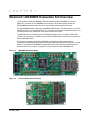
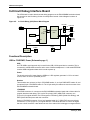
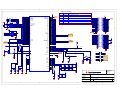
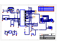
Stellaris® EK-LM3S9B90 Evaluation Kit User ’s Manual EK-LM3S9B90 -0 4 Co pyrigh t © 2 009– 201 0 Te xas In strumen ts Copyright Copyright © 2009–2010 Texas Instruments, Inc. All rights reserved. Stellaris and StellarisWare are registered trademarks of Texas Instruments. ARM and Thumb are registered trademarks, and Cortex is a trademark of ARM Limited. Other names and brands may be claimed as the property of others. Texas Instruments 108 Wild Basin, Suite 350 Austin, TX 78746 http://www.ti.com/stellaris 2 January 6, 2010 Stellaris® LM3S9B90 Evaluation Kit User’s Manual Table of Contents Chapter 1: Stellaris® LM3S9B90 Evaluation Kit Overview ........................................................................... 7 Kit Contents ........................................................................................................................................................ 8 Using the EK-LM3S9B90.................................................................................................................................... 8 Features.............................................................................................................................................................. 8 Chapter 2: Hardware Description .................................................................................................................. 11 Evaluation Board .............................................................................................................................................. 11 Functional Description .................................................................................................................................. 11 In-Circuit Debug Interface Board ...................................................................................................................... 14 Functional Description .................................................................................................................................. 14 Chapter 3: Software Development ................................................................................................................ 17 Software Description......................................................................................................................................... 17 Source Code..................................................................................................................................................... 17 Tool Options ..................................................................................................................................................... 17 Programming the EK-LM3S9B90 Board........................................................................................................... 17 Appendix A: Schematics................................................................................................................................ 19 Appendix B: Connection Details ................................................................................................................... 25 Component Locations....................................................................................................................................... 25 Board Dimensions ............................................................................................................................................ 26 Board Connectivity............................................................................................................................................ 27 References ....................................................................................................................................................... 27 Appendix C: Microcontroller GPIO Assignments ........................................................................................ 29 January 6, 2010 3 List of Figures Figure 1-1. Figure 1-2. Figure 2-1. Figure 2-2. Figure 2-3. Figure 2-4. Figure 2-5. Figure 2-6. Figure 2-7. Figure 2-8. Figure B-1. Figure B-2. Figure B-3. Figure B-4. Figure B-5. 4 LM3S9B90 Evaluation Board .......................................................................................................... 7 In-Circuit Debug Interface Board..................................................................................................... 7 EK-LM3S9B90 Evaluation Board Block Diagram.......................................................................... 11 GPIO Pads .................................................................................................................................... 12 JTAG/SWD Connector .................................................................................................................. 12 PWR/UART Connector.................................................................................................................. 13 In Circuit Debug (ICDI) Board Block Diagram ............................................................................... 14 JTAG/SWD Connector J1 ............................................................................................................. 15 JTAG/SWD Connector J3 ............................................................................................................. 15 PWR/UART Connector.................................................................................................................. 15 EK-LM3S9B90 Evaluation Board Component Locations .............................................................. 25 BD-ICDI Board Component Locations .......................................................................................... 25 EK-LM3S9B90 Evaluation Board Dimensions .............................................................................. 26 In-Circuit Debug Interface Board Dimensions ............................................................................... 26 ICDI – EK-LM3S9B90 Board Connectivity .................................................................................... 27 January 6, 2010 List of Tables Table C-1. EK-LM3S9B90 Evaluation Board GPIO Usage............................................................................. 29 January 6, 2010 5 6 January 6, 2010 C H A P T E R 1 Stellaris® LM3S9B90 Evaluation Kit Overview Luminary Micro's Stellaris® LM3S9B90 Evaluation Board Kit (EK-LM3S9B90) is a low-cost platform for evaluation of the LM3S9B90 microcontroller. The kit includes two boards, the EK-LM3S9B90 evaluation board, and the In-Circuit Debug Interface (BD-ICDI) board. The EK-LM3S9B90 board includes the LM3S9B90 ARM® Cortex™-M3 Microcontroller, a 10/100 Mbit Ethernet port, a full-speed USB-OTG port, connectors for inteface to the BD-ICDI board, and oversized pads for easy connection to the microcontroller GPIO ports. The BD-ICDI board is a USB full-speed JTAG/SWD debugger board. It includes a USB miniB connector for connection to a USB PC port, and two shrouded header connectors for connection to the EK-LM3S9B90 board. Development of software for the EK-LM3S9B90 is simplified by using Luminary Micro's comprehensive StellarisWare® peripheral driver library and ARM development tools from our tools partners. The Stellaris® LM3S9B90 Evaluation Board Kit includes the two boards described, a documentation CD, and cables. All design files are provided on the EK-LM3S9B90 CD. Figure 1-1. LM3S9B90 Evaluation Board Figure 1-2. In-Circuit Debug Interface Board January 6, 2010 7 Stellaris® LM3S9B90 Evaluation Kit Overview Kit Contents The EK-LM3S9B90 evaluation kit comes with the following: EK-LM3S9B90 evaluation board In-Circuit Debug Interface (BD-ICDI) board – Connects to USB port on PC and to 10-pin, fine-pitch ARM JTAG connector on the EK-LM3S9B90 evaluation board – Secondary 8-pin Power/UART connector provides power and virtual comm-port capability to the EK-LM3S9B90 evaluation board. Cables – USB miniB to USB-A cable – USB-OTG to USB-A cable – 10-pin ribbon cable for JTAG/SWD connection – 8-pin ribbon cable for Power/UART connection CD containing: – A supported version of one of the following (including a toolchain-specific Quickstart guide): • Keil™ RealView® Microcontroller Development Kit (MDK-ARM) • IAR Embedded Workbench • Code Sourcery GCC development tools • Code Red Technologies development tools • Texas Instruments’ Code Composer Studio™ IDE – Complete documentation – Quickstart application source code – Stellaris® Firmware Development Package with example source code Using the EK-LM3S9B90 The recommended steps for using the EK-LM3S9B90 evaluation kit are: 1. Follow the Quickstart guide included in the kit. The Quickstart guide will help get the EK-LM3S9B90 LC Evaluation Board up and running in minutes. 2. Use your preferred ARM tool-chain and the Luminary Micro Peripheral Driver Library to develop an application. Software applications are loaded using the BD-ICDI board. See Chapter 3, “Software Development,” for the programming procedure. The StellarisWare Peripheral Driver Library Software Reference Manual contains specific information on software structure and function. 3. Customize and integrate the hardware to suit an end application. This user's manual is an important reference for understanding circuit operation and completing hardware modification. Features The EK-LM3S9B90 evaluation kit provides the following features: 8 January 6, 2010 Stellaris® LM3S9B90 Evaluation Kit User’s Manual LM3S9B90 high-performance Stellaris microcontroller and large memory – 32-bit ARM® Cortex™-M3 core – 256 KB single-cycle Flash memory, 96 KB single-cycle SRAM, 23.7 KB single-cycle ROM Ethernet 10/100 port with two LED indicators USB 2.0 Full-Speed OTG port Virtual serial communications port capability Oversized board pads for GPIO access User pushbutton and LED Detachable ICDI board can be used for debugging other Luminary Micro boards Easy to customize – Includes full source code, example applications, and design files – Develop using tools supporting FastMATH from Keil, IAR, Code Sourcery, and Code Red (using a Stellaris evaluation kit or preferred ARM Cortex-M3 debugger) – Supported by Luminary Micro StellarisWare peripheral driver library January 6, 2010 9 Stellaris® LM3S9B90 Evaluation Kit Overview 10 January 6, 2010 C H A P T E R 2 Hardware Description The EK-LM3S9B90 evaluation kit contains two boards: the EK-LM3S9B90 evaluation board and the BD-ICDI JTAG debug board as described in more detail in this chapter. Evaluation Board The EK-LM3S9B90 evaluation board uses the Stellaris® LM3S9B90 microcontroller and includes a 10/100 Ethernet port and a USB 2.0 full-speed OTG port. The board is intended for use with the ICDI board, but can be used as a standalone board as well. Figure 2-1 shows the block diagram. Figure 2-1. EK-LM3S9B90 Evaluation Board Block Diagram Ethernet 10/100 BOARD PADs GPIOs Ethernet 25MHz RESET USER LED Stellaris LM3S9B90 JTAG/SWD USER PUSHBUTTON JTAG USB – OTG USB USB Power Switch PWR/UART UART0 MOSC 16MHz RTC 4.19MHz 5V VBUS DPDT 3.3V Regulator Functional Description Microcontroller, Reset, GPIO Pads, and JTAG (Schematic page 1) Microcontroller The evaluation board uses the Stellaris LM3S9B90 microcontroller. A 16 MHz crystal provides the main oscillator clock which can directly drive the ARM core clock or can drive an internal PLL to increase the core clock up to 80 MHz. A 25 MHz crystal is used for the Ethernet clock and a 4.194304 MHz crystal is used for the real-time clock. The LM3S9B90 microcontroller has an internal LDO voltage regulator that supplies power for internal use. This rail requires only three capacitors for decoupling and is not connected to any other circuits. January 6, 2010 11 Hardware Description Reset A reset switch and R-C network connects to the microcontroller’s RSTn input. The reset signal is also connected to the JTAG/SWD connector J1 to allow reset control from the debugger. GPIO Pads Four groups of oversized board pads with a 0.1” spacing provide access to GPIO signals and standard 0.1” pitch headers can be soldered to these pads. Pads are labeled with the corresponding GPIO signal, and pads with no labels are unconnected. Note that GPIO signals required for operation of the Ethernet port, USB port, and JTAG port are reserved for board use and are not available on these pads. Figure 2-2 shows the pad groups. GPIO Pads PG 0 2 PJ 0 PJ PJ GN D PA 7 PA 6 PA 5 PA 4 PA 3 PA 2 V GN D 3.3 PF 5 PF 4 PF 3 PF 2 PF 0 PE 0 PE 1 PE 2 PE 3 PE 4 PE 5 PE 6 PE 7 R PB 2 PB 3 PB 4 PB 5 PB 6 PB 7 GN D GPIO Pads – Bottom right 5V PA 1 PA 0 5V GPIO Pads – Bottom left 1 PG 7 VB US PH 0 PH 1 PH 2 PH 5 PH 6 PH 7 PG 1 7 6 PD 5 PD 4 PD GPIO Pads – Top right HI B W AK E VB AT 3 PD 2 PC 7 SH DN PD 1 PD PC 6 PD PC 5 PC 4 PD 0 GPIO Pads – Top left PF 1 Figure 2-2. GPIO Jumpers Some of the GPIO signals used by the board are connected to board jumpers and can be disconnected to provide additional user GPIOs. GPIOs PA0/PA1/PB4/PD0/PF2/PF3 are connected to jumpers JR1-JR6 respectively. Each signal can be freed by cutting the trace of the corresponding jumper (cut at white line on silkscreen). The jumper pads have the same footprint as an 0603 SMT resistor. To reconnect a previously cut jumper, solder a 0 ohm resistor to the corresponding jumper footprint. JTAG/SWD The JTAG/SWD connector J1 is used for program download and debug. This is a 2x5 fine pitch (0.050”) ARM JTAG connector, see (Figure 2-3) for signal definition. The LM3S9B90 microcontroller supports JTAG debug, Serial Wire Debug (SWD), and Serial Wire Out (SWO) trace with this connector. The ICDI board connects via a 10-wire ribbon cable to this connector. Figure 2-3. JTAG/SWD Connector 10 9 In In Out In I/O RSTn TDI TDO/SWO TCK/SWCLK TMS/SWDIO GND N/C GND GND 3.3V Out 2 1 12 January 6, 2010 PWR/UART The PWR/UART connector J2 is used to provide 5 V power from the ICDI board and also to connect the LM3S9B90 UART0 signals. This is a 2x4 fine pitch (0.050") connector, see (Figure 2-4) for signal definition. The UART0 signals are connected to GPIO jumpers JR1 and JR2 and can be disconnected from connector J2 if required, see “GPIO Jumpers” on page 12. The ICDI board connects via an 8-wire ribbon cable to this connector. Figure 2-4. PWR/UART Connector 8 7 In In Out 5V N/C VCP_RX VCP_TX 5V N/C GND GND In 2 1 Ethernet, USB, Power and Miscellaneous (Schematic page 2) Page 2 of the schematics contains the Ethernet RJ45 connector, USB power switch and USB OTG connector, 3.3 V regulator, and power switch selector. Ethernet Port The on-board RJ45 connector provides a 10/100 base T Ethernet port. The RJ45 connector includes integrated LEDs and magnetics. The LEDs are connected to GPIO jumpers JR4 and JR5 and can be disconnected from the RJ45 connector if required, see GPIO Jumpers section. USB Port The on-board USB microAB connector provides a USB 2.0 full-speed port. To use as an On-TheGo (OTG) port, the power selector switch SW3 lever must be set to EXT. This selects an external 5 V power source to provide power to the board and the USB power switch. If the SW3 lever is set to USB, power to the board is received from USB, the on-board USB power switch output is disconnected from USB, and the board can only be used as a USB device. When using the USB-OTG port in Host mode, the current provided to a USB device should be limited to 100 mA or less when powered from the ICDI board. If powered from the 5 V test pad, then this can be increased to 500 mA. Board Power The board requires 5 V for operation, and switch SW3 is used to select the power source. If the switch lever is moved towards the USB label on the board, power is received from the USB connector. If the switch lever is moved towards the EXTernal board label, the board is powered from the PWR/UART connector and the ICDI board provides power to this connector. DC regulator U2 generates 3.3 V for powering the board circuits and includes power indicator LED D1. User Devices Pushbutton switch SW2 and LED D2 are available for the user and connected to PB4 and PD0 respectively. These GPIOs are connected to GPIO jumpers JR3 and JR4 and can be disconnected from SW2 and D2 if required, see GPIO Jumpers section. January 6, 2010 13 Hardware Description In-Circuit Debug Interface Board The ICDI board is used to download and debug programs on the EK-LM3S9B90 evaluation board, but can also be used for debug of other Luminary Micro boards. A block diagram is shown in Figure 2-5. Figure 2-5. In Circuit Debug (ICDI) Board Block Diagram JTAG/SWD USB 2x10 USB JTAG/SWD 2x5 PortA PortB JTAG/SWD MUX FTDI EEPROM PWR /UART 2x4 DEBUG ACTIVE OSC 6MHz VBUS RESET POWER 3.3V Regulator Functional Description USB to JTAG/SWD, Power (Schematic page 1) USB An FTDI USB to serial protocol chip is used for the USB 2.0 full-speed device controller. This is connected to a USB miniB connector and to a set of buffers/multiplexers. A 1-kbit serial EEPROM contains USB configuration data which is read at power up. Power The board receives 5 V power from the USB bus. A DC regulator generates 3.3 V for on-board circuits, when on LED D1 (POWER) is lit on. Headers Three headers are on-board, a 10-pin JTAG/SWD header J1, an 8-pin PWR/UART header J2, and an optional 20-pin JTAG/SWD header J3. The 10-pin and 8-pin headers are used to connect to the EK-LM3S9B90 evaluation board. JTAG/SWD JTAG/SWD connector J1 connects to the EK-LM3S9B90 evaluation board with a ribbon cable for program download and debug. This is a 2x5 fine pitch (0.050”) ARM JTAG connector, see (Figure 2-6) for signal definition.The ICDI supports JTAG debug, SWD (Serial Wire Debug), and SWO (Serial Wire Out) trace with this connector. Optional JTAG/SWD connector J3 is a 2x10 standard pitch (0.1”) ARM JTAG connector directly connected to J1, see (Figure 2-7) for signal definition. This allows the ICDI to connect to targets that use a 2x10 connector. It also allows the use of an external 2x10 debugger on targets with the 14 January 6, 2010 fine pitch connector, including the EK-LM3S9B90. The signal direction shown for J1 and J3 applies when the ICDI is used as the JTAG/SWD debugger and LED D2 (DEBUG ACTIVE) is lit on. In this case only one of the two connectors J1/J3 should be used. The ICDI can also be used as a 20-pin to 10-pin adapter for external JTAG debuggers. Note that the DEBUG ACTIVE LED must be off before connecting any external JTAG debuggers. Figure 2-6. JTAG/SWD Connector J1 10 9 Out Out In Out I/O SRSTn TDI TDO/SWO TCK/SWCLK TMS/SWDIO GND N/C GND GND VSENSE In 2 1 Figure 2-7. JTAG/SWD Connector J3 20 19 GND GND GND GND GND GND GND GND GND N/C N/C N/C SRSTn TDO/SWO N/C TCK/SWCLK TMS/SWDIO TDI N/C VSENSE 2 Out In Out I/O Out In 1 Pushbutton Pushbutton SW1 (RESET) is provided to manually generate the SRSTn signal to the target device. The SRSTn signal can also be generated under program control. PWR/UART The PWR/UART connector J2 connects to the EK-LM3S9B90 evaluation board with a ribbon cable and provides 5 V power and a virtual communications port connection. This is a 2 x 4 fine pitch (0.050”) connector, see (Figure 2-8) for signal definition. Signals DBG1/DBG2 are reserved. Figure 2-8. PWR/UART Connector 8 7 Out Out In 5V DBG2 VCP_RX VCP_TX 5V DBG1 GND GND Out 2 1 January 6, 2010 15 Hardware Description JTAG / SWD Multiplexer (Schematic page 2) Buffers A set of tri-state buffers is used to multiplex JTAG and SWD signals, and also multiplex the UART VCP_TX signal with the SWO signal. LED D2 (DEBUG ACTIVE) is lit on when these buffers are enabled. To avoid signal contention, external JTAG debuggers should not be connected when DEBUG ACTIVE is on. 16 January 6, 2010 C H A P T E R 3 Software Development This chapter provides general information on software development as well as instructions for Flash memory programming. Software Description The software provided with the EK-LM3S9B90 provides access to all of the peripheral devices supplied in the design. The StellarisWare® Peripheral Driver Library is used to operate the on-chip peripherals. The software includes a set of example applications that utilize the StellarisWare Peripheral Driver Library. These applications demonstrate the capabilities of the LM3S9B90 microcontroller, as well as providing a starting point for the development of the final application for use on the EK-LM3S9B90. Source Code The complete source code is included on the EK-LM3S9B90 CD. Refer to the Quickstart Guide for a detailed description of hardware setup and how to install the source code. The source code and binary files are installed in the DriverLib tree. Tool Options The source code installation includes directories containing projects and/or makefiles for the following tool-chains: Keil ARM RealView® Microcontroller Development System IAR Embedded Workbench for ARM CodeSourcery G++ Code Red Technology Red Suite Generic Gnu C compiler Evaluation versions of these tools may be downloaded from www.ti.com/stellaris. Due to code size restrictions, the evaluation tools may not build all example programs. A full license is necessary to re-build or debug all examples. Instructions on installing and using each of the evaluation tools can be found in the Quickstart guides (for example, Quickstart-Keil, Quickstart-IAR) which are available for download from the evaluation kit section of our web site at www.ti.com/stellaris. For detailed information on using the tools refer to the documentation included in the tool chain installation or visit the website of the tools supplier. Programming the EK-LM3S9B90 Board The EK-LM3S9B90 software package includes pre-built binaries for each of the example applications. If you installed DriverLib to the default installation path of C:/DriverLib, you can find the example applications in “C:/DriverLib/boards/ek-tempest”. The ICDI board is used along with Luminary Micro's LM Flash Programmer tool to program applications on the EK-LM3S9B90 board. January 6, 2010 17 Software Development To program example applications into the EK-LM3S9B90 evaluation board using the ICDI board: 1. Install LM Flash Programmer on a Windows PC. 2. Connect the 10-wire ribbon cable to the 10-pin header on the ICDI board and to the 10-pin header on the EK-LM3S9B90 board. The red stripe on the ribbon cable should be facing the bottom of the connectors (see Figure B-5 on page 27). 3. Connect the 8-wire ribbon cable to the 8-pin header on the ICDI board and to the 8-pin header on the EK-LM3S9B90 board. The red stripe on the ribbon cable should be facing the bottom of the connectors (see Figure B-5 on page 27). 4. Verify that slide switch SW3 on the EK-LM3S9B90 board is set to EXTernal. 5. Connect the USB cable A-plug to an available port on the PC and the miniB-plug to the ICDI board. 6. Verify that POWER LED D1 on the ICDI board is lit and POWER LED D1 on the EK-LM3S9B90 board is also lit. 7. Run LM Flash Programmer. 8. In the Configuration tab, use the Quick Set control to select LM3S9B90 Evaluation Board. 9. Move to the Program tab and click the Browse button. Navigate to the example applications directory (the default location is “C:/DriverLib/boards/ek-tempest/). 10. Each example application has its own directory. Navigate into the example directory that you want to load and then into the directory which contains the binary (*.bin) files. Select the binary file and click Open. 11. Set the “Erase Method” to “Erase Necessary Pages” and check the “Verify After Program” box. 12. Next, click the Program button to start the Erase, Download and Verify process. The DEBUG ACTIVE LED (D2) on the ICDI will turn on at this time. 13. Program execution will start once Verify is complete. The EK-LM3S9B90 design uses a Stellaris® LM3S9B90 microcontroller to handle networking, USB-OTG, and peripheral functions. The entire circuit is built on a compact four-layer printed circuit board. All design files are provided on the EK-LM3S9B90 CD. 18 January 6, 2010 A P P E N D I X A Schematics This section contains the schematics for the EK-LM3S9B90 evaluation board and also the BD-ICDI debug board. EK-LM3S9B90 Evaluation Board Microcontroller, Reset, and Headers on page 20 Ethernet, USB, and Power on page 21 BD-ICDI Board USB to JTAG, SWD, Headers, and Power on page 22 JTAG/SWD Multiplexer on page 23 January 6, 2010 19 Schematic page 1 1 2 3 4 5 6 Revision History VBUS Revision Date A 2/24/2009 First release for prototypes. B 4/15/2009 Released to production. U1 10K 10K 10K 10K 3.3V J1 1 3 5 7 9 C1 0.1uF 2 4 6 8 10 TMS TCK TDO TDI RSTn HDR 2X5-MH-SHRD 5V JTAG/SWD J2 8 6 4 2 DBG2 VCP_RX VCP_TX 7 5 3 1 DBG1 HDR 2X4-MH-SHRD PWR/UART 26 27 28 29 30 31 34 35 PC0 PC1 PC2 PC3 PC4 PC5 PC6 PC7 80 79 78 77 25 24 23 22 PE0 PE1 PE2 PE3 PE4 PE5 PE6 PE7 74 75 95 96 6 5 2 1 PG0 PG1 XTALN XTALP PF5 PG7 19 18 17 16 41 40 37 36 OSCin OSCout 48 49 B ETH_RXIP ETH_RXIN 3.3V HIBn R24 10K 3.3V PA0/U0RX PA1/U0TX PA2/SSI0CLK PA3/SSI0FSS PA4/SSI0RX PA5/SSI0TX PA6 PA7 PC0/TCK/SWCLK PC1/TMS/SWDIO PC2/TDI PC3/TDO/SWO PC4 PC5 PC6 PC7 PE0 PE1 PE2 PE3 PE4 PE5 PE6 PE7 PG0 PG1 XTALNPHY XTALPPHY PF5 RXIP RXIN PG7 OSC0 OSC1 4 3 1 2 RESET R23 51 10 RSTn 33 C2 C 64 0.1uF PD0 PD1 PD2 PD3 PD4 PD5 PD6 PD7 PF0 PF1 PF2/LED1 PF3/LED0 MDIO TXON TXOP PF4 PH0 PH1 PH2 PH3/USB0EPEN PH4/USB0PFLT PH5 PH6 PH7 HIB PJ0 PJ1 PJ2 WAKEn XOSC0 XOSC1 GND VBAT RST USB0DP USB0DM SW1 R6 10K PB0/USB0ID PB1/USB0VBUS PB2/I2C0SCL PB3/I2C0SDA PB4 PB5 PB6 PB7 ERBIAS USB0RBIAS Y2 GND GND GND GND GND GND GND VDD33 VDD33 VDD33 VDD33 VDD33 VDD33 VDD33 VDD33 CVDD CVDD Y1 1 2 4 25.000 MHz C15 18pF 16.000 MHz C16 18pF 10 11 12 13 97 98 99 100 PD0 PD1 PD2 PD3 PD4 PD5 PD6 PD7 47 61 60 59 58 46 43 42 PF0 PF1 PF2 PF3 86 85 84 83 76 63 62 15 PH0 PH1 PH2 14 87 39 50 52 53 54 55 PJ0 PJ1 PJ2 PC4 PC5 PC6 PC7 HIBn WAKEn VBAT C17 18pF C18 18pF AGND AVDD PF4 USBPWR USBFLT PH5 PH6 PH7 PE0 PE1 PE2 PE3 PE4 PE5 PE6 PE7 PG0 PJ0 PJ1 PJ2 3.3V R5 10K WAKEn LM3S9B90 D C3 0.1uF 8 20 32 44 56 68 81 93 A 3.3V B PD0 PD1 PD2 PD3 PD4 PD5 PD6 PD7 PF0 PF1 PF2 PF3 PF4 PF5 VBUS PG1 PG7 PH0 PH1 PH2 PH5 PH6 PH7 7 FB1 JR1 VCP_RX PA1 JR2 VCP_TX PB4 JR3 PD0 JR4 PF2 JR5 PF3 JR6 1M C4 4.194304 MHz 18pF 3.3V 38 88 PA0 Y3 C7 0.1uF C8 0.1uF C9 0.1uF C10 0.1uF C11 0.1uF C12 0.1uF C13 0.1uF C14 0.1uF C5 18pF USR_PBn C USR_LED ETH_LED1 ETH_LED0 C6 1uF Texas Instruments CVDD C19 0.1uF C20 0.1uF 108 Wild Basin Rd. Suite 350 Austin, TX 78746 C22 Designer: Drawing Title: Page Title: Tempest, Reset, Test Pads Approved: Size Document Number: B * Date: 4 D EK-LM3S9B90 Evaluation Board Arnaldo Cruz 1uF Arnaldo Cruz 3 TP52 TP53 TP54 TP55 TP56 TP57 TP58 TP59 TP60 TP61 TP62 TP63 TP64 TP65 TP66 TP67 TP68 5VR XOSC1 Drawn by: 2 TP35 TP36 TP37 TP38 TP39 TP40 TP41 TP42 TP43 TP44 TP45 TP46 TP47 TP48 TP49 TP50 TP51 PB2 PB3 PB4 PB5 PB6 PB7 9.1k R7 C23 0.1uF 1 TP18 TP19 TP20 TP21 TP22 TP23 TP24 TP25 TP26 TP27 TP28 TP29 TP30 TP31 TP32 TP33 TP34 XOSC0 USBDP USBDM VBAT 3 TP1 TP2 TP3 TP4 TP5 TP6 TP7 TP8 TP9 TP10 TP11 TP12 TP13 TP14 TP15 TP16 TP17 SHDNn ETH_MDIO ETH_TXON ETH_TXOP 71 70 73 5V PA0 PA1 PA2 PA3 PA4 PA5 PA6 PA7 R9 LDO 2 PB2 PB3 PB4 PB5 PB6 PB7 USBID R8 12.4K 9 21 45 57 69 82 94 1 66 67 72 65 92 91 90 89 120ohm @ 100 MHz R1 R2 R3 R4 A PA0 PA1 PA2 PA3 PA4 PA5 PA6 PA7 Description 5 Rev 0001 5/18/2009 B Sheet 1 6 of 2 Schematic page 2 1 2 3 4 5 6 3.3V J5 G1 VBUS USB Micro AB VBUS D- D+ ID C25 0.1uF G2 G VUSB FB2 R11 330 R12 330 5 4 3 1 A 2 R10 10K R13 49.9 R14 49.9 A FB3 120ohm @ 100 MHz J6 120ohm @ 100 MHz G+ 12 11 USBDM USBDP USBID G- ETH_MDIO 3 ETH_TXOP ETH_TXON R25 C27 10pF USR_LED 3.3V 10 RX+ 3 4 R26 10 5 RX- 6 1CT:1 7 6 8 8 B R16 49.9 C29 10pF R17 49.9 2 1 Y- 9 10 NC Y+ PulseJack_RJ45_SMT C31 0.1uF 5VR B GND C30 10pF GL GR ETH_LED1 ETH_LED0 D2 GREEN_LED USR 3 2 TX+ 1 TX- 2 5 7 USR PB USR_PBn 1CT:1 4 C28 10pF ETH_RXIP ETH_RXIN R18 330 R15 10K 4 1 SW2 VBUS C26 0.01uF ETHERNET 10/100 C32 0.01uF 5V 1 SW3 2 3 4 5 6 SHDNn 3.3V Switch DPDT 3.3V U2 R19 10K 5V 4 R21 10K 3 C 2 USBFLT C33 4.7uF VIN VOUT GND NR PQ1LA333MSPQ VOUT USBPWR U3 5 R22 10K C36 C37 4.7uF 4 0.1uF 2 VIN VOUT EN OC 5 R20 330 SHDN C34 4.7uF 1 C35 D1 GREEN_LED PWR 0.1uF 1 C 3 C38 4.7uF GND TPS2051B CVDD U4 1 R27 10K 3 2 VIN EN VOUT ADJ GND PG 6 5 R28 113K Note: U4, R27, R28, and R29 required only for LM3S9B90 rev B1. See errata. 4 FAN2558ADJ D FID1 40 Mil Pad 100 Mil Mask FID2 40 Mil Pad 100 Mil Mask FID3 40 Mil Pad 100 Mil Mask Drawing Title: D EK-LM3S9B90 Evaluation Board R29 100K Page Title: Fiducials Ethernet, USB, Power Size Document Number: B Date: 1 2 3 4 5 Rev B 0001 5/18/2009 Sheet 2 6 of 2 Schematic page 1 1 2 3 4 5 6 Revision History 3.3V Revision J4 USB_MINI_B_RECEPTACLE G3 5V D- D+ ID G4 G G1 G2 5 4 3 1 5V 2 R1 10K A 120ohm @ 100 MHz 6 3V3OUT FB2 120ohm @ 100 MHz USBM R5 27 UDM 8 USBP R6 27 UDP 7 5V 5V USBDM USBDP R10 10K U2 C2 0.1uF 8 7 6 5 VCC NC ORG GND CS SK DI DO 1 2 3 4 R9 EECS EESK EEDATA 48 1 2 47 XTI XTO 43 44 2.21k CAT93C46 1K 64X16 24 23 22 21 20 19 17 16 ADBUS0 ADBUS1 ADBUS2 ADBUS3 ADBUS4 ADBUS5 ADBUS6 ADBUS7 ACBUS0 ACBUS1 ACBUS2 ACBUS3 SI/WUA R7 1.50k R8 10K B R3 10K R4 10K 4 5 1 2 6.000MHz C7 18pF 45 C8 18pF First release for prototypes. B 4/03/2009 Released for production. A EECS EESK EEDATA TEST XTIN XTOUT RESET# RSTOUT# BDBUS0 BDBUS1 BDBUS2 BDBUS3 BDBUS4 BDBUS5 BDBUS6 BDBUS7 FT_SK FT_DO FT_DI FT_CS DBGRSTn DBGENn DBGMOD 15 13 12 11 10 VSENSE 40 39 38 37 36 35 33 32 VCP_RX VCP_TX_SWO R11 10K TCK TMS_SWDIO TDI TDO_SWO VCP_TX_SWO J3 SWO_EN 20 18 16 14 12 10 8 6 4 2 DBG1 DBG2 30 29 28 27 26 BCBUS0 BCBUS1 BCBUS2 BCBUS3 SI/WUB 41 PWREN# 3.3V 9 18 25 34 Y1 Description 2/24/2009 U1 C1 0.1uF VBUS FB1 R2 10K Date A GND GND GND GND J1 10 8 6 4 2 9 7 5 3 1 HDR 2X5-MH-SHRD JTAG/SWD 2X10 HDR-SHRD 5V JTAG/SWD 3 42 14 31 VCC VCC VCCIOA VCCIOB AGND B 19 17 15 SRSTn 13 TDO 11 9 TCK 7 TMS 5 TDI 3 1 C3 0.1uF R12 475 46 AVCC C4 0.1uF C5 0.1uF C6 0.1uF 5V C9 0.1uF FT2232 J2 C DBG2 VCP_RX VCP_TX 13 3.3V 2 U5D SN74LVC125A 5 R15 330 SHDN GND NR SRSTn 10 D2 GREEN_LED DEBUG ACTIVE C12 4.7uF 1 D1 GREEN_LED PWR PQ1LA333MSPQ SW1 Texas Instruments RESET 2 C13 0.1uF 4 10K C11 4.7uF VOUT R19 108 Wild Basin Rd. Suite 350 Austin, TX 78746 3 R14 VIN 11 1 3 Designer: D Drawing Title: Drawn by: Page Title: USB to JTAG, SWD Arnaldo Cruz Approved: Size Date: 3 4 Document Number: B * 2 D In Circuit Debug Interface (ICDI) Board Arnaldo Cruz 1 DBG1 R13 330 3.3V U3 4 C 7 5 3 1 HDR 2X4-MH-SHRD PWR/UART 12 5V 8 6 4 2 5 Rev 0001 5/18/2009 B Sheet 1 6 of 2 Schematic page 2 1 2 3 4 5 6 FT_SK FT_DO FID1 40 Mil Pad 100 Mil Mask 13 A 11 R16 27 FID3 40 Mil Pad 100 Mil Mask A TCK 1 12 FID2 40 Mil Pad 100 Mil Mask 2 Fiducials U4D SN74LVC125A 3 U5A 3.3V SN74LVC125A R20 10K 10 DBGMOD 9 8 R17 27 R18 27 R21 10K TDI 4 DBGENn U4C SN74LVC125A 6 2 FT_CS 3 B TMS_SWDIO 1 U6A SN74LVC126A 3 U4A SN74LVC125A 4 2 R22 10K 5 6 3.3V 14 U6B SN74LVC126A U4E SN74LVC125A GND 7 9 VCC GND 7 8 FT_DI U5E SN74LVC125A VCC GND 7 10 VCC 14 B 1 U5B SN74LVC125A 14 5 U6E SN74LVC126A TDO_SWO U6C SN74LVC126A C 3.3V 4 C 6 5 C14 0.1uF C15 0.1uF C16 0.1uF 13 U4B SN74LVC125A 11 VCP_TX_SWO 12 U6D SN74LVC126A 10 SWO_EN 8 D 9 Drawing Title: VCP_TX Page Title: U5C SN74LVC125A JTAG, SWD Mux Size Document Number: B Date: 1 2 3 D In Circuit Debug Interface (ICDI) Board 4 5 Rev B 0001 4/9/2009 Sheet 2 6 of 2 24 January 6, 2010 A P P E N D I X B Connection Details This appendix contains the following sections: Component Locations (see page 25) Board Dimensions (see page 26) Board Connectivity (see page 27) References (see page 27) Component Locations Figure B-1. EK-LM3S9B90 Evaluation Board Component Locations Figure B-2. BD-ICDI Board Component Locations January 6, 2010 25 Board Dimensions Board Dimensions Figure B-3. EK-LM3S9B90 Evaluation Board Dimensions 4.00 0.07 0.07 Ø 0.100 0.34 1.40 0.07 0.07 0.07 0.07 Figure B-4. In-Circuit Debug Interface Board Dimensions 2.50 0.07 0.07 Ø 0.100 1.40 0.07 0.07 26 0.07 January 6, 2010 Stellaris® LM3S9B90 Evaluation Kit User’s Manual Board Connectivity Figure B-5. ICDI – EK-LM3S9B90 Board Connectivity 8-wire cable BD-ICDI Board PWR/UART EK-LM3S9B90 Evaluation Board JTAG/SWD 10-wire cable References In addition to this document, the following references are included on the Stellaris Evaluation Kit CD-ROM and are also available for download at www.ti.com/stellaris: Stellaris LM3S9B90 Data Sheet, publication DS-LM3S9B90 StellarisWare Driver Library StellarisWare Driver Library User’s Manual, publication SW-DRL-UG Additional references include: FT2232D Dual USB/UART FIFO IC Datasheet, version 0.91, 2006, Future Technology Devices International Ltd. Information on development tool being used: – RealView MDK web site, www.keil.com/arm/rvmdkkit.asp – IAR Embedded Workbench web site, www.iar.com – Code Sourcery GCC development tools web site, www.codesourcery.com/gnu_toolchains/arm – Code Red Technologies development tools web site, www.code-red-tech.com – Texas Instruments’ Code Composer Studio™ IDE web site, www.ti.com/ccs January 6, 2010 27 References 28 January 6, 2010 A P P E N D I X C Microcontroller GPIO Assignments The following table shows the LM3S9B90 GPIOs used by the EK-LM3S9B90 board. All other GPIOs are available for use and accessible on the test pads. Table C-1. EK-LM3S9B90 Evaluation Board GPIO Usage Port Function Board Signal PA0 U0RX VCP_RX Usage Description Virtual Communications port receive signal from J2 header. To disconnect from header cut JR1 jumper. UART PA1 U0TX VCP_TX PB0 USB0ID USBID PB1 USB0VBUS VBUS PB4 GPIO USR_PBn PC0 TCK/SWCLK PC0 PC1 TMS/SWDIO PC1 PC2 TDI PC2 PC3 TDO/SWO PC3 PD0 GPIO USR_LED PF2 LED1 ETH_LED1 Virtual Communications port transmit signal to J2 header. To disconnect from header cut JR2 jumper. USBID signal from the USB-On-the-Go connector J5. USB User USB VBUS input signal from USB-OTG connector J5 for sensing VBUS levels. Input from user pushbutton SW2. To disconnect from pushbutton cut JR3 jumper. JTAG or SWD clock input JTAG/ SWD JTAG TMS input or SWD bidirectional signal SWDIO JTAG TDI signal input. JTAG TDO output or SWD trace signal SWO output. User Output to user LED D2. To disconnect from LED cut JR4 jumper. Output to RJ45 jack J6 yellow LED. To disconnect from LED cut JR5 jumper. Ethernet PF3 PH3 LED0 USB0EPEN ETH_LED0 Output to RJ45 jack J6 green LED. To disconnect from LED cut JR6 jumper. USBPWR Output to USB-OTG power switch U3. When set high it enables the USB-OTG power switch to provide USB VBUS power to USB-OTG connector J5. When set low power switch U3 is disabled. USB PH4 January 6, 2010 USB0PFLT USBPFLT Overcurrent input status from USB-OTG power switch U3. When high the power switch status is normal. When low an overcurrent condition has been detected by the switch. 29 30 January 6, 2010 IMPORTANT NOTICE Texas Instruments Incorporated and its subsidiaries (TI) reserve the right to make corrections, modifications, enhancements, improvements, and other changes to its products and services at any time and to discontinue any product or service without notice. Customers should obtain the latest relevant information before placing orders and should verify that such information is current and complete. All products are sold subject to TI’s terms and conditions of sale supplied at the time of order acknowledgment. TI warrants performance of its hardware products to the specifications applicable at the time of sale in accordance with TI’s standard warranty. Testing and other quality control techniques are used to the extent TI deems necessary to support this warranty. Except where mandated by government requirements, testing of all parameters of each product is not necessarily performed. TI assumes no liability for applications assistance or customer product design. Customers are responsible for their products and applications using TI components. To minimize the risks associated with customer products and applications, customers should provide adequate design and operating safeguards. TI does not warrant or represent that any license, either express or implied, is granted under any TI patent right, copyright, mask work right, or other TI intellectual property right relating to any combination, machine, or process in which TI products or services are used. Information published by TI regarding third-party products or services does not constitute a license from TI to use such products or services or a warranty or endorsement thereof. Use of such information may require a license from a third party under the patents or other intellectual property of the third party, or a license from TI under the patents or other intellectual property of TI. Reproduction of TI information in TI data books or data sheets is permissible only if reproduction is without alteration and is accompanied by all associated warranties, conditions, limitations, and notices. Reproduction of this information with alteration is an unfair and deceptive business practice. TI is not responsible or liable for such altered documentation. Information of third parties may be subject to additional restrictions. Resale of TI products or services with statements different from or beyond the parameters stated by TI for that product or service voids all express and any implied warranties for the associated TI product or service and is an unfair and deceptive business practice. TI is not responsible or liable for any such statements. TI products are not authorized for use in safety-critical applications (such as life support) where a failure of the TI product would reasonably be expected to cause severe personal injury or death, unless officers of the parties have executed an agreement specifically governing such use. Buyers represent that they have all necessary expertise in the safety and regulatory ramifications of their applications, and acknowledge and agree that they are solely responsible for all legal, regulatory and safety-related requirements concerning their products and any use of TI products in such safety-critical applications, notwithstanding any applications-related information or support that may be provided by TI. Further, Buyers must fully indemnify TI and its representatives against any damages arising out of the use of TI products in such safety-critical applications. TI products are neither designed nor intended for use in military/aerospace applications or environments unless the TI products are specifically designated by TI as military-grade or "enhanced plastic." Only products designated by TI as military-grade meet military specifications. Buyers acknowledge and agree that any such use of TI products which TI has not designated as military-grade is solely at the Buyer's risk, and that they are solely responsible for compliance with all legal and regulatory requirements in connection with such use. TI products are neither designed nor intended for use in automotive applications or environments unless the specific TI products are designated by TI as compliant with ISO/TS 16949 requirements. Buyers acknowledge and agree that, if they use any non-designated products in automotive applications, TI will not be responsible for any failure to meet such requirements. Following are URLs where you can obtain information on other Texas Instruments products and application solutions: Products Applications Amplifiers amplifier.ti.com Audio www.ti.com/audio Data Converters dataconverter.ti.com Automotive www.ti.com/automotive DLP® Products www.dlp.com Communications and Telecom www.ti.com/communications DSP dsp.ti.com Computers and Peripherals www.ti.com/computers Clocks and Timers www.ti.com/clocks Consumer Electronics www.ti.com/consumer-apps Interface interface.ti.com Energy www.ti.com/energy Logic logic.ti.com Industrial www.ti.com/industrial Power Mgmt power.ti.com Medical www.ti.com/medical Microcontrollers microcontroller.ti.com Security www.ti.com/security RFID www.ti-rfid.com Space, Avionics & Defense www.ti.com/space-avionics-defense RF/IF and ZigBee® Solutions www.ti.com/lprf Video and Imaging www.ti.com/video Wireless www.ti.com/wireless-apps Mailing Address: Texas Instruments, Post Office Box 655303, Dallas, Texas 75265 Copyright © 2010, Texas Instruments Incorporated