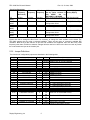
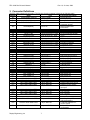
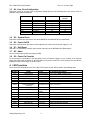
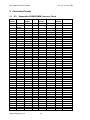
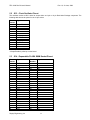
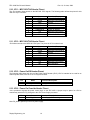
1
Zephyr Engineering, Inc.
User’s Manual, ZPC.1900, Rev. B
Rev 1.2
23 June, 2003
Preliminary
Copyright 2003 Zephyr Engineering, Inc.
All rights Reserved.
The information presented within this manual is preliminary and is subject to
change without notice.
ZPC.1900 Rev B User’s Manual
Rev 1.2, 23 June, 2003
1.
INTRODUCTION................................................................................................................... 1
2.
ZPC.1900 FEATURES AND SETUP.................................................................................... 1
2.1
Feature List ....................................................................................................................................... 1
2.2
Block Diagram .................................................................................................................................. 2
2.2.1
MPC8265.................................................................................................................................... 2
2.2.2
SDRAM ...................................................................................................................................... 2
2.2.3
Boot Flash................................................................................................................................... 2
2.2.4
Flash SIMM................................................................................................................................ 3
2.2.5
Security Processors..................................................................................................................... 3
2.2.6
PMC Slot .................................................................................................................................... 3
2.2.7
EEPROM .................................................................................................................................... 3
2.2.8
Ethernet....................................................................................................................................... 3
2.2.9
RS-232 ........................................................................................................................................ 3
2.2.10 TCOM Expansion Slot ............................................................................................................... 3
2.2.11 User IO Expansion Port .............................................................................................................. 3
2.3
Hardware Setup ................................................................................................................................ 3
2.3.1
Power Supply.............................................................................................................................. 3
2.3.2
Console Port ............................................................................................................................... 3
2.3.3
Memory Requirements ............................................................................................................... 4
2.3.4
PCI or Local Bus Mode Selection .............................................................................................. 4
2.3.5
MPC8265 Clock Configuration .................................................................................................. 4
2.3.6
Jumper Definitions...................................................................................................................... 5
2.4
Software Setup .................................................................................................................................. 6
2.4.1
Default Memory Map ................................................................................................................. 6
2.4.2
Boot Flash................................................................................................................................... 6
3.
CONNECTOR DEFINITIONS ............................................................................................... 7
SWITCHES AND DEBUG FUNCTIONS ......................................................................................... 8
3.1
S1 – User Setting Switches ............................................................................................................... 8
3.2
S2, S3 – User Chip Select Isolation.................................................................................................. 8
3.3
S4 - User Clock Configuration......................................................................................................... 9
3.4
S5 – System Reset.............................................................................................................................. 9
3.5
S6 – Power On/Off ............................................................................................................................ 9
3.6
S7 – Soft Reset................................................................................................................................... 9
3.7
S8 – Abort.......................................................................................................................................... 9
3.8
S9 – Power On Override .................................................................................................................. 9
4.
LED FUNCTIONS ................................................................................................................. 9
Zephyr Engineering, Inc
i
ZPC.1900 Rev B User’s Manual
Rev 1.2, 23 June, 2003
5.
CONNECTOR PINOUTS .................................................................................................... 10
5.1
JD1 – Expandable SDRAM DIMM Connector Pinout ............................................................... 10
5.2
JD3 – Clock Oscillator Pinout ....................................................................................................... 11
5.3
JD4 – Expandable FLASH SIMM Socket Pinout ........................................................................ 11
5.4
JP1 – General Purpose User Logic Header Pinout...................................................................... 12
5.5
JP2 – Logic JTAG Header Pinout................................................................................................. 12
5.6
JP4 – LXT972A JTAG Header Pinout ......................................................................................... 13
5.7
JP5 – System Reset Header Pinout................................................................................................ 13
5.8
JP7 – PMC JTAG Header Pinout ................................................................................................. 13
5.9
JP10 – MPC8265 JTAG Header Pinout ....................................................................................... 13
5.10
JP11 – MPC185 JTAG Header Pinout ......................................................................................... 14
5.11
JP13 – MPC180 JTAG Header Pinout ......................................................................................... 14
5.12
JP15 – Power On/Off Header Pinout ............................................................................................ 14
5.13
JP16 – Power On Override Header Pinout .................................................................................. 14
5.14
P1, P2, P3 – User IO Port Pinouts ................................................................................................. 15
5.15
P4, P5 – TCOM Port Pinouts......................................................................................................... 17
5.16
P6A, P6B – Ethernet Port Pinouts ................................................................................................ 17
5.17
P7A, P7B – Serial Communication Port Pinouts ......................................................................... 17
5.18
P9 – ATX Power Supply Connector Pinout.................................................................................. 18
5.19
P10, P11 – PMC Card Connector Pinouts.................................................................................... 18
5.20 P12 through P20 – Logic Analyzer Connector Pinouts ............................................................... 19
5.20.1 Connector P12 – 60x Bus Address ........................................................................................... 19
5.20.2 Connector P13 – 60x Bus Data (High) ..................................................................................... 19
5.20.3 Connector P14 – 60x Bus Data (Low)...................................................................................... 20
5.20.4 Connector P15 – 60x Bus Control ............................................................................................ 20
5.20.5 Connector P16 – 60x Bus Memory Control and IRQs ............................................................. 20
5.20.6 Connector P17 – MPC8265 Port A........................................................................................... 21
5.20.7 Connector P18 – MPC8265 Port B........................................................................................... 21
5.20.8 Connector P19 – MPC8265 Port C........................................................................................... 21
5.20.9 Connector P20 – MPC8265 Port D........................................................................................... 22
5.20.10
Connector P21 – Local Bus Data - PCI Bus Address/Data................................................... 22
5.20.11
Connector P22 – Local Bus Address – PCI Bus Control...................................................... 23
5.20.12
Connector P23 – Local Bus / PCI Bus Control..................................................................... 23
Zephyr Engineering, Inc
ii
ZPC.1900 Rev B User’s Manual
Rev 1.2, 23 June, 2003
6.
SYSTEM INITIALIZATION PROGRAMMING .................................................................... 24
6.1
Hard Reset Configuration Word................................................................................................... 24
6.2
MPC8265 System Control Register Programming...................................................................... 24
6.3
Memory Controller Register Programming................................................................................. 25
6.4
Chip Select, IDSEL and Interrupt Mapping ................................................................................ 26
6.5
PCI IDSEL ...................................................................................................................................... 26
7.
LOCAL REGISTER DEFINITIONS..................................................................................... 26
7.1
FLASH Presence Detect ................................................................................................................. 26
7.2
User Switch Register....................................................................................................................... 26
7.3
Board Revision Register................................................................................................................. 27
7.4
LED Register................................................................................................................................... 27
7.5
Mode Register ................................................................................................................................. 27
8.
OPTIONAL CONFIGURATIONS........................................................................................ 27
8.1
Peripheral Isolation ........................................................................................................................ 27
8.2
PCI Configuration Resistors.......................................................................................................... 27
9.
WARRANTY AND SUPPORT INFORMATION ................................................................. 28
9.1
Warranty ......................................................................................................................................... 28
9.2
Support ............................................................................................................................................ 28
Zephyr Engineering, Inc
iii
ZPC.1900 Rev B User’s Manual
Rev 1.2, 23 June, 2003
1. Introduction
Zephyr Engineering’s ZPC.1900 Security Processor Development Platform is an ATX form-factor Single Board
Computer featuring a PowerPC MPC8265 CPU. This feature rich platform provides a versatile environment for
evaluation, development and demonstration of many members of the Motorola Security Processor family. On
board are two Security Processors, the MPC185 and MPC180. Additional Security Processors are supported
via a 32 bit 66/33 MHz PMC slot. Optional PMC plug in modules for the MPC190 and MPC184 may be
purchased from Zephyr Engineering. For more information on these products please visit: www.zpci.com.
2. ZPC.1900 Features and Setup
2.1
•
•
•
•
•
•
•
•
•
•
•
•
•
•
•
•
•
•
Feature List
MPC8265 CPU – 266 MHz
MPC185 Security Processor
MPC180 Security Processor
64 MB of 64 Bit SDRAM
4 MB Flash SIMM
2 MB On-Board Flash Boot Rom
8 KB EEPROM
8 MB Local Bus SDRAM
2 Ethernet Ports – 1 10/100BaseT, 1 10BaseT
2 RS232 Ports
32 Bit 66/33 MHz PMC Slot
JTAG Connector for MPC8265 On-Chip Debug Port
Interrupt Status LEDs
User Defined LEDs
User Defined Switches
High Speed Logic Analyzer Connectors (AMP Mictor)
Standard ATX Form-factor
Uses Standard ATX Power Supply
Zephyr Engineering, Inc
1
ZPC.1900 Rev B User’s Manual
2.2
Rev 1.2, 23 June, 2003
Block Diagram
CS2#
CS3#
LOGIC ANALYZER CONNECTORS
16M x 64
SDRAM
DIMM
P. 7
P. 7
P. 8
P. 12
P12 TO P23
JD1
RN62 - RN77
USER I/O PORTS
60X CONTROL BUS
IRQ0#
P. 17
P1,P2,P3
60X ADDRESS BUS / 32
60X DATA BUS / 64
RN38 - RN40
FAST ETHERNET PORT
BADDR[27..31]
A[7..28]
MA[0..13]
IRQ3#
ADDRESS
BUFFER
DATA
BUFFER
P. 8
PLD ADDR
MUX
P. 8
P. 7
BA[7..28]
P. 16
SDAMUX
DBUFEN#
BAA[27..31]
PA
MPC8265
CPU
10BASE-T PORT
PB
LXT905
P. 14
RN45
PD
RS-232 COM1 & COM2
BA[7..28]
IRQ1#
P. 9
4M x 32
FLASH
(SIMM)
P. 8
P. 3, 4, 5
LB / PCI DATA
PCI / PMC SLOT
PCI CONTROL
P. 15
JD4
P10,P11
IRQ4#
IRQ5#
P. 15
LB ADDRESS
P. 15
RN11 - RN22, RN28
TCOM BOARD SLOT
IRQ6#
IRQ7#
JP9
LB
1M x 16
FLASH
(ON-BOARD)
P7,P8
LB / PCI DATA
LB CONTROL
PCI
P. 16
P4,P5
CS9#
2M x 32
LOCAL BUS
SDRAM
(OPT)
P. 8
P. 7
MPC180
SECURITY
PROCESSOR
(OPT)
16
8
EXP
ADDRESS
BUFFER
P. 16
BA
EBA
16
BCSR2CS#
P. 9
CS4#
CS5#
MAX3223
P. 14
16
CS6#
P6B
PC
MPC8260
(OPT)
32
CS0#
CS1#
P6A
RN42 - RN43
MPC185
SECURITY
PROCESSOR
(OPT
SOCKET) JD2
P. 10, 11
BD[0..31]
LXT972A
P. 14
16
BD
EXP
DATA
BUFFER
P. 16
CS8#
IRQ2#
8K x 8
EEPROM
SRESET
EBD
16
TDBUFEN#
SRESET#
P. 8
S7
JD5
3.3V
ABORT
VCC
IRQ0#
+3.3V
S8
+5.0V
VCC
BCSR2CS#
TDBUFEN#
FLASH
DETECT
HRESET#
P. 13
S5
USER
LOGIC
USER
LOGIC
+5.0V
ATX POWER
CONNECTOR
+12V
-12V
MAX700
P. 6
-12V
PWRESET#
P. 5
R44
5.1
25W
P. 13
P9
S6
P. 13
USER SW
& LEDS
PWR ON/OFF
GND
CS7#
EXTERNAL
ATX POWER
SUPPLY
+12V
GND
S9
GND
ZEPHYR ENGINEERING, INC.
1620 WEST FOUNTAINHEAD PARKWAY, SUITE 320
TEMPE, ARIZONA 85282-1876
PWR OVRRD
Title
ZPC.1900 PLATFORM
Size
C
Document Number
Date:
Friday, November 29, 2002
Rev
B
BLOCK DIAGRAM
Sheet
2
of
17
2.2.1 MPC8265
The MPC8265 is a member of the PowerQuicc II communications processor family. This CPU features:
• MPC603e core
• Core frequencies up to 266 MHz
• Separate 16Kbyte instruction and data caches
• 64 bit data, 32 bit address 60x bus
• Selectable PCI or MPC8260 style Local bus
• Integrated memory controller
• Communications Processor Module
2.2.2 SDRAM
The ZPC.1900 provides a standard 168 pin DIMM socket for memory expansion. The standard platform ships
with 64 MB of SDRAM.
2.2.3 Boot Flash
A 2 Mbyte AMD Am29F016 2Mx8 Flash ROM is provided. Boot code shipped with the board contains a
minimal debugger and either a VxWorks image bootloader or UBOOT for Linux.
Zephyr Engineering, Inc
2
ZPC.1900 Rev B User’s Manual
Rev 1.2, 23 June, 2003
2.2.4 Flash SIMM
On board is an 80 pin SIMM socket for a Flash DIMM module. The socket allows up to 16MB Flash modules to
be used. A 2M x 32 (8 Mbyte) module is provided with the ZPC.1900 platform.
2.2.5 Security Processors
Two Motorola Security Processors are featured on the ZPC.1900 board.
• MPC185 – The ZPC.1900 is configured in multi-master mode for the 60x bus, allowing optimum
performance for security applications.
• MPC180 - In Local Bus Mode a Motorola MPC180 Security Processor is connected to the local bus side
of the MPC8265.
2.2.6 PMC Slot
In PCI Mode, a 32 Bit 66/33 MHz PMC slot is available. General purpose PMC IO boards or additional
Security Processors such as the MPC190 on Zephyr Engineering’s ZPCI.3900 or the MPC184 (ZPCI.3901)
may be used in this slot.
2.2.7 EEPROM
An 8Kx8 Atmel AT28HC64B EEPROM is provided for non-volatile user parameter storage.
2.2.8 Ethernet
The MPC8265’s embedded Communication Processor Module (CPM) hosts 2 ethernet controllers. Physical
interfaces and magnetics are implemented on the ZPC.1900 board. For the 10/100 Fast Ethernet port an
LXT972 interface is used. For the 10BASET port the physical interface is an LXT905.
2.2.9 RS-232
Two RS-232 ports are driven from the MPC8265’s Serial Communications Controller to an on board RS-232
level translator.
2.2.10 TCOM Expansion Slot
This port is for future expansion.
2.2.11 User IO Expansion Port
Many of the MPC8265 control and CPM signals are pinned out to a User IO port consisting of three 96 pin DIN
type connectors. These may be used by users for additional hardware prototyping.
2.3
Hardware Setup
The ZPC.1900 ships with default configuration options that make it usable right out of the box for most users.
This section describes the options that will most commonly be modified or referred to by a user.
2.3.1 Power Supply
The ZPC.1900 uses a standard PC ATX power supply. The power supply connects to the board at P9. See
section 7.20 for P9 pin definitions.
Many ATX power supplies require a load on the +5VDC power that exceeds the minimal amount of current
consumed by the ZPC.1900. For platforms that have no other connections to the power supply and use little or
no current on +5VDC, a power load resistor is provided on the board. The load resistor is enabled by placing a
jumper on JP17.
2.3.2 Console Port
Two RS-232 Serial ports are provided on the ZPC.1900 at P7. The upper connector is defined to be the
console port by the on board boot rom. This connector is a standard 9 pin male D-Sub connector and has the
same pin out as a standard PC serial port. Transmit data out TXD is on pin 3 and receive data in RXD is on
Zephyr Engineering, Inc
3
ZPC.1900 Rev B User’s Manual
Rev 1.2, 23 June, 2003
pin 2. Ground is on pin 5. A null modem (cross over) cable is required to connect the platform to a standard
PC serial port.
2.3.3 Memory Requirements
Standard 168 pin, 64 Bit SDRAM DIMMs are used in socket JD1. A 64 MB SDRAM DIMM is provided with the
board.
2.3.4 PCI or Local Bus Mode Selection
The MPC8265 and ZPC.1900 board may be configured to operate in one of two modes:
1. PCI Bus Mode
2. Local Bus Mode
By default, the PCI Bus Mode is configured at the factory.
Each mode hosts certain features that are available only when the CPU and the ZPC.1900 board are
configured for that mode. The table below defines these features.
Function/Device
60x Bus SDRAM (main memory)
2 MB On-board Boot Rom Flash
8 MB Flash SIMM
8 KB EEPROM
Board Control/Status Registers
MPC185 Security Processor
8 MB Local Bus SDRAM
MPC180 Security Processor
TCOM Expansion Slot
PMC PCI Slot
Available in Mode
Both
Both
Both
Both
Both
Both
Local Bus
Local Bus
Local Bus
PCI Bus
In addition to software that must initialize the MPC8265, the ZPC.1900 board configuration must match the
mode being selected. The following options/jumpers/switches vary according to the option being configured:
1. Reset Configuration Word (programmed into boot flash)
2. User Clock Configuration Switches (S4)
3. PCI / Local Bus Select Jumper (JP9)
2.3.5 MPC8265 Clock Configuration
The MPC8265 supports a large number of clock frequency configurations (see the MPC8260 User Manual,
Section 9 as well as the PCI Bridge Functional Specification Addendum). This configuration is accomplished
by sampling the MODCK pins at reset and when in local bus mode by reading designated bits of the reset
configuration word from the boot rom. Some of the MODCK pins are user configurable via the switches at S4.
Other pins are set by zero ohm option resistors that may be populated or de-populated on the board. The table
below shows the default configuration of the ZPC.1900. The default configuration may be too conservative for
users wishing to demonstrate performance or run benchmarks. For users who may be connecting and
debugging prototype hardware to the platform, the default settings may be too aggressive. Alternate
configurations are also shown below.
Zephyr Engineering, Inc
4
ZPC.1900 Rev B User’s Manual
Clock Configurations
MODE
Input Clock
Frequency
(Bus Clock)
Rev 1.2, 23 June, 2003
CPM
Frequency
CPU Core
Frequency
MODCK_H
Set by option resistors in
PCI
MODE.
Set
by
RSTCONF in LB MODE
0000 Configuration Resistors
MODCK[1-3]
Set by S4[2-4]
PCI
MODE
Local Bus
MODE
66 MHz
133 MHz
166 MHz
66 MHz
133 MHz
133 MHz
0x05
from
Configuration Word
PCI
MODE
Local Bus
MODE
Local Bus
MODE
66 MHz
200 MHz
266 MHz
0000 Configuration Resistors
111 [OFF-OFF-OFF]
66 MHz
133 MHz
266 MHz
Reset
001 [ON-ON-OFF]
33 MHz
133 MHz
233 MHz
0x06
from
Configuration Word
0x02
from
Configuration Word
Reset
010 [ON-OFF-ON]
Reset
000 [ON-ON-ON]
101 [OFF-ON-OFF]
Please note that to change the Bus Clock it is necessary to change the main oscillator on the board. The
ZPC.1900 supports this by using a socketed oscillator. There are two types of commonly available DIP
oscillators. Both the 8 pin DIP and the 16 pin DIP size oscillators are supported. Also note that if any CPM
frequency other than 133 MHz is selected, changes will also need to be done to the boot rom code to provide
the correct baud rate input to the console port.
2.3.6 Jumper Definitions
The functions of configuration jumpers are described in the following table.
Jumper
JP3
Jumper Name
LB SDRAM ENABLE
Default
X
Pins
open
shorted
Functional Description
enable clock to local bus SDRAM
disable clock to local bus SDRAM
JP6
GROUND CONNECTION
X
open
shorted
float logic ground from chassis ground
connect logic ground to chassis ground
JP8
PCI CLK SEL
X
open
shorted
66MHz PCI clock
33MHz PCI clock
JP9
PCI/LB SEL
X
1-2
2-3
Select PCI Bus Mode
Select Local Bus Mode
JP12
ENDIAN CONTROL
1-2
3-4
5-6
7-8
0 -> MPC180 Endian control pin
1 -> MPC180 Endian control pin
PA1 -> MPC180 Endian control pin
LA17 -> MPC180 Endian control pin
1-3
2-4
1-2
3-4
Boot from on-board 2MB FLASH
X
JP14
JP17
CS0# BOOT SELECT
ENABLE 5V 1A LOAD
Zephyr Engineering, Inc
X
X
open
shorted
5
Boot from 8MB FLASH SIMM
disconnect 5 ohm load
connect 5 ohm load to 5V bus
ZPC.1900 Rev B User’s Manual
2.4
Rev 1.2, 23 June, 2003
Software Setup
2.4.1 Default Memory Map
Device
Main Memory – 64 MB
Local Bus SDRAM – 8MB
MPC180
Board
Control/Status
Registers
8KB EEPROM
MPC185
PMC Slot
8MB SIMM Flash
2MB on-board Boot Flash
Recommended Address
0x00000000 – 0x03FFFFFF
0x04000000 – 0x047FFFFF**
0x05000000 – 0x05FFFFFF**
0x21000000 – 0x2100FFFF
0x22000000
0x30000000
0x60000000
0xE0000000
0xFE000000
–
–
–
–
–
0x2200FFFF
0x37FFFFFF
0x6FFFFFFF
0xE0FFFFFF
0xFFFFFFFF
** These devices are not available in the default PCI Bus Mode configuration
2.4.2 Boot Flash
The on-board boot rom contains a minimal debugger and bootloader.
It is also possible to boot from the Flash SIMM module. The ZPC.1900 ships with a copy of the on-board flash
boot rom image programmed onto the Flash SIMM module. This provides a backup should the on-board copy
be accidentally erased or corrupted. To boot from the SIMM module simply change the direction of the two
jumpers on JP14 from both horizontal to both vertical. The default position of both horizontal connects chip
select CS0 to the on board flash and CS6 to the Flash SIMM module. The alternate jumper position reverses
these connections, connecting CS0 to the Flash SIMM module and CS6 to the on-board flash.
Zephyr Engineering, Inc
6
ZPC.1900 Rev B User’s Manual
Rev 1.2, 23 June, 2003
3. Connector Definitions
The ZPC.1900 contains 39 connectors. The function of each connector is listed in the following table.
Number
Name
Type
Functional Description
JD1
EXPANDABLE SDRAM
168-pin DIMM
System Memory
JD2
MPC185
256-pin BGA
Security Processor
JD3
CLK OSC
14-pin DIP
Provides Bus Clock to CPU
JD4
EXPANDABLE FLASH
80-pin SIMM
Boot Flash backup +
parameter storage
JD5
EPROM(8Kx8)
PLCC-32
Stores System Boot
Parameters
JP1
JP2
JP4
JP5
JP7
G/P USER LOGIC
LOGIC JTAG
LXT972A JTAG
SYSTEM RESET
PMC JTAG
20-pin dual-row 2mm pitch
10-pin dual-row 0.1” pitch
8-pin dual-row 0.1” pitch
2-pin 2mm pitch
8-pin sgl-row 0.1” pitch
HW prototyping resource
PLD Programming header
JTAG
In parallel with S5
JTAG for PMC board
JP10
JP11
JP13
MPC826x JTAG
MPC185 JTAG
MPC180 JTAG
16-pin dual-row 0.1” pitch
10-pin dual-row 0.1” pitch
10-pin dual-row 0.1” pitch
Emulator connection
Component JTAG
Component JTAG
JP15
JP16
POWER ON/OFF
POWER ON OVERRIDE
2-pin 2mm pitch
2-pin 2mm pitch
In parallel with S6
In parallel with S9
P1
P2
P3
P4
P5
P6A
P6B
P7A
P7B
P9
P10
P11
USER IO PORT
USER IO PORT
USER IO PORT
TCOM PORT P1
TCOM PORT P2
10BASE-T
FAST ETHERNET
COM1 (upper)
COM2 (lower)
POWER SUPPLY CONNECTOR
PMC CARD P10
PMC CARD P11
96-pin DIN - F
96-pin DIN - F
96-pin DIN - F
128-pin DIN - F
128-pin DIN - F
RJ-45
RJ-45
DB-9M
DB-9M
20-pin male ATX
64-pin PMC
64-pin PMC
HW prototyping resource
HW prototyping resource
HW prototyping resource
Future Expansion
Future Expansion
10BT Ethernet
100BT Ethernet
Console Port
nd
2 RS-232 Port
ATX Power Supply input
PMC board slot
PMC board slot
P12
P13
P14
P15
P16
MPC LOGIC ANALYZER
MPC LOGIC ANALYZER
MPC LOGIC ANALYZER
MPC LOGIC ANALYZER
MPC LOGIC ANALYZER
38-pin MICTOR
38-pin MICTOR
38-pin MICTOR
38-pin MICTOR
38-pin MICTOR
P17
P18
P19
P20
MPC LOGIC ANALYZER
MPC LOGIC ANALYZER
MPC LOGIC ANALYZER
MPC LOGIC ANALYZER
38-pin MICTOR
38-pin MICTOR
38-pin MICTOR
38-pin MICTOR
60x Bus Address
60x Bus Data (high) [0-31]
60x Bus Data (low) [32-63]
60x Bus Control Signals
CPU Chip select and
Interrupts
Port A signals
Port B signals
Port C signals
Port D signals
P21
LB/PCI LOGIC ANALYZER
38-pin MICTOR
P22
LB/PCI LOGIC ANALYZER
38-pin MICTOR
P23
LB/PCI LOGIC ANALYZER
38-pin MICTOR
Zephyr Engineering, Inc
7
Local Bus Data / PCI
Address/Data Bus
Local Bus Address/ PCI
control signals
PCI control + clock
configuration
ZPC.1900 Rev B User’s Manual
Rev 1.2, 23 June, 2003
Switches and Debug Functions
There are 9 switches on the ZPC.1900. The function of each switch is listed in the following table.
Number
S1
Name
USER SETTING
Type
DIP-8
Functional Description
User defined – read by software at 0x21000001
S2
USER CHIP SELECT ISOLATION
DIP-8
For debugging, each CS may be isolated from CPU
S3
USER CHIP SELECT ISOLATION
DIP-8
For debugging, each CS may be isolated from CPU
S4
USER CLOCK CONFIG
DIP-8
Configures CPU clock ratios
S5
SYSTEM RESET
PBT-mom
Connects to CPU HRESET#
S6
POWER ON/OFF
PBT-mom
Controls power supply on/off
S7
SOFT RESET
PBT-mom
Connects to CPU SRESET#
S8
ABORT
PBT-mom
Connects to MPC8265 IRQ0
S9
POWER ON OVERRIDE
toggle
3.1
Bypass on-board power switch logic to use power
switch on power supply
S1 – User Setting Switches
The state of these user defined switches can be read from the User Switches register at 0x21000001.
3.2
S2, S3 – User Chip Select Isolation
Each of the Chip Selects driven from the MPC8265 memory controller passes through a user configurable chip
select isolation switch. For debugging purposes, individual chip selects may be isolated from the CPU by
setting the appropriate switch to the OFF position. The default configuration is all switches ON.
Switch
S2-1
S2-2
S2-3
S2-4
S2-5
S2-6
S2-7
S2-8
S3-1
S3-2
S3-3
S4-4
S4-5
S4-6
S4-7
Zephyr Engineering, Inc
Chip Select
CS0
CS1
CS2
CS3
CS4
CS5
CS6
CS7
CS8
CS9
CS10
CS11
None
None
None
8
Device
Boot Flash
Reserved for Flash Expansion
SDRAM
Reserved for SDRAM Expansion
Local Bus SDRAM
EEPROM
Flash SIMM
Board Control/Status Registers
MPC180
TCOM Expansion Slot
Not Used
Not Used
Not Connected
Not Connected
Not Connected
ZPC.1900 Rev B User’s Manual
3.3
Rev 1.2, 23 June, 2003
S4 - User Clock Configuration
Switch S4 is used to set user clock configuration settings shown in the following table. See section 2.3.5 for
alternate configuration possibilities.
3.4
Switch
Name
Local Bus Mode
S4-1
S4-2
S4-3
S4-4
S4-5
S4-6
S4-7
S4-8
not used
MODCK1
MODCK2
MODCK3
not used
not used
not used
RSTCONF
off
off
on
off
off
off
off
on
PCI Bus Mode
(default)
off
on
on
on
off
off
off
on
S5 – System Reset
Switch S5 is debounced and used to drive both HRESET# and PWRESET# to the MPC8265.
3.5
S6 – Power On/Off
Switch S6 is debounced to generate a control signal that is used to turn the power supply on / off.
3.6
S7 – Soft Reset
Switch S7 is a momentary normally open contact connecting to the MPC8265 Soft Reset signal.
3.7
S8 – Abort
S8 is a normally open switch connecting to IRQ0.
3.8
S9 – Power On Override
For some users it is preferable to use the switch on the ATX power supply or to use a switch on an external
power strip rather than the switch on the ZPC.1900 to turn power on and off. For this function S9 is provided to
bypass the power control logic on the ZPC.1900.
4. LED Functions
There are 9 LED assemblies on the ZPC.1900. The function of each LED is listed in the following table.
Number
LED1
Name
USER LEDS
Type
4-stack RED
Functional Description
top = bit 7 (MSB); bottom = bit 4
LED2
USERLEDS
4-stack GRN
top = bit 3; bottom = bit 0 (LSB)
LED3
10BASE STATUS
3-stack R-Y-G
R=TX; Y=RX; G=Link
LED4
FAST ETHERNET
STATUS
3-stack R-Y-G
R=?; Y=?; G=?
LED5
POWER
Board edge
GRN
On = +5V active
LED6
ACTIVE
smt GRN
Driven by 60x Bus DBB# signal
LED7
DEBUG
smt YEL
Driven by QREQ# signal
LED8
MPC185-INT
smt YEL
MPC185 interrupt asserted
LED9
MPC180-INT
smt YEL
MPC180 interrupt asserted
Zephyr Engineering, Inc
9
ZPC.1900 Rev B User’s Manual
Rev 1.2, 23 June, 2003
5. Connector Pinouts
5.1
JD1 – Expandable SDRAM DIMM Connector Pinout
Pin
Number
1
2
3
4
5
6
7
8
9
10
11
12
13
14
15
16
17
18
19
20
21
22
23
24
25
26
27
28
29
30
31
32
33
34
35
36
37
38
39
40
41
42
43
44
45
46
47
Signal
GND
D0
(MSB)
D1
D2
D3
3.3V
D4
D5
D6
D7
D8
Gnd
D9
D10
D11
D12
D13
3.3V
D14
D15
NC
NC
GND
NC
NC
3.3V
WE#
WE0#
WE1#
CS2#
NC
GND
MA0
MA2
MA4
MA6
MA8
MA10
MA13
3.3V
3.3V
CLK0
GND
NC
CS2#
WE2#
WE3#
Pin
Number
48
49
50
51
52
53
54
55
56
57
58
59
60
61
62
63
64
65
66
67
68
69
70
71
72
73
74
75
76
77
78
79
80
81
82
83
84
85
86
87
88
89
90
91
92
93
94
Zephyr Engineering, Inc
Signal
Signal
WE#
3.3V
Pin
Number
95
96
NC
NC
NC
NC
GND
D16
D17
D18
D19
3.3V
D20
NC
NC
CKE
GND
D21
D22
D23
GND
D24
D25
D26
D27
3.3V
D28
D29
D30
D31
GND
CK2
NC
NC
SDA
SCL
3.3V
GND
D32
D33
D34
D35
3.3V
D36
D37
D38
D39
97
98
99
100
101
102
103
104
105
106
107
108
109
110
111
112
113
114
115
116
117
118
119
120
121
122
123
124
125
126
127
128
129
130
131
132
133
134
135
136
137
138
139
140
141
D41
D42
D43
D44
D45
3.3V
D46
D47
NC
NC
GND
NC
NC
3.3V
CAS#
WE4#
WE5#
CS2#
RAS#
GND
MA1
MA3
MA5
MA7
MA9
MA12
MA11
3.3V
CK1
GND
GND
CKE
CS3#
WE6#
WE7#
GND
3.3V
NC
NC
NC
NC
GND
D48
D49
D50
10
D40
GND
Pin
Number
142
143
Signal
144
145
146
147
148
149
150
151
152
153
154
155
156
157
158
159
160
161
162
163
164
165
166
167
168
D52
NC
NC
NC
GND
D53
D54
D55
GND
D56
D57
D58
D59
3.3V
D60
D61
D62
D63
GND
CK3
NC
SA0
SA1
SA2
3.3V
D51
3.3V
ZPC.1900 Rev B User’s Manual
5.2
Rev 1.2, 23 June, 2003
JD3 – Clock Oscillator Pinout
The oscillator socket at JD3 is wired to accept either an 8 pin or 14 pin Dual-Inline-Package component. The
following table shows the pinout for the 16 pin socket.
Pin
Number
1
2
3
4
5
6
7
8
9
10
11
12
13
14
Signal
Output Enable**
NC
NC
GND
NC
NC
GND
OUTPUT
NC
NC
OUTPUT
NC
NC
3.3V
**Output Enable is pulled up on the board.
5.3
JD4 – Expandable FLASH SIMM Socket Pinout
Pin
Number
1
2
3
4
5
6
7
8
9
10
11
12
13
14
15
16
17
18
19
20
21
22
23
24
25
26
Signal
GND
+5V
VPP (+5V)
OE#
WE0#
WE1#
RESET#
D23
D22
D21
D20
D19
D18
D17
D16
D31
D30
D29
D28
D27
NC
NC
CS1#
CS6# **
GND
D26
Zephyr Engineering, Inc
Pin
Number
41
42
43
44
45
46
47
48
49
50
51
52
53
54
55
56
57
58
59
60
61
62
63
64
65
66
Signal
A18
A19
A20
A21
A22
A23
A24
A25
A26
A27
A28
A29
WE3#
GND
D8
D9
D10
D11
D12
D13
D14
D15
D0
D1
D2
D3
11
ZPC.1900 Rev B User’s Manual
27
28
29
30
31
32
33
34
35
36
37
38
39
40
5.4
D25
D24
WE2#
A7
A8
A9
A10
A11
A12
A13
A14
A15
A16
A17
67
68
69
70
71
72
73
74
75
76
77
78
79
80
Rev 1.2, 23 June, 2003
D4
D5
D6
D7
VPP (+5V)
+5V
PD1
PD2
PD3
PD4
PD5
PD6
PD7
GND
JP1 – General Purpose User Logic Header Pinout
JP1 may be used to monitor the state of control signals connecting to the User Logic PLD U1 and/or to add
future capabilities. The “IOxx” signals connect to the PLD and are currently unused.
G/P USER LOGIC
PIN OUT
JP1
TDBUFEN#
LOGIC1
TCOM_CS9#
IO53
IO55
IO58
IO60
IO62
IO64
GCLR#
1
3
5
7
9
11
13
15
17
19
2
4
6
8
10
12
14
16
18
20
BCSR2CS#
LOGIC2
PCI_MODE#
IO54
IO57
IO59
IO61
IO63
OE1
OE2
HEADER 10X2
5.5
JP2 – Logic JTAG Header Pinout
JP2 is used to program both the User Logic PLD (U1) and the SDRAM multiplexer PLD U10. Both
components are Altera CPLD parts and are programmed with the Altera ByteBlaster cable. The following table
shows the pinout for JP2.
Zephyr Engineering, Inc
Pin
1
2
3
Name
TCK
GND
TDO
4
5
6
7
8
9
+5V
TMS
NC
GND
NC
TDI
10
GND
12
Functional Description
JTAG Clock Signal
Ground
JTAG Data Out (from
SDRAM multiplexer)
Power
JTAG TMS
No Connection
Ground
No Connection
JTAG Data In (to user
pld)
Ground
ZPC.1900 Rev B User’s Manual
5.6
Rev 1.2, 23 June, 2003
JP4 – LXT972A JTAG Header Pinout
The following table shows the pinout of the LXT972A JTAG header (JP4).
Pin
1
2
3
4
5
6
7
8
5.7
Name
TRST_L
ground
TCK
ground
TMS
ground
TDO
TDI
Functional Description
LXT972 pin 31
power ground
LXT972 pin 30
power ground
LXT972 pin 29
power ground
LXT972 pin 28
LXT972 pin 27
JP5 – System Reset Header Pinout
The following table shows the pinout of the Reset header (JP5).
JP5 is intended to be used for an external reset switch, such as on an ATX system chassis
Pin
1
2
5.8
Name
reset
ground
Functional Description
low causes reset assertion; logic holds low for 500 ms
power ground
JP7 – PMC JTAG Header Pinout
The following table shows the pinout of the PMC JTAG connector (JP7).
Pin
1
2
3
4
5
6
7
8
5.9
Name
+3.3V
PMC_TDO
PMC_TDI
PMC_TRST#
PMC_TMS
ground
PMC_TCK
Functional Description
+3.3V power
PMC chain TDO
PMC chain TDI
PMC chain TRST#
<key>
PMC chain TMS
power ground
PMC chain TCK
JP10 – MPC8265 JTAG Header Pinout
JP10 is provided for connecting an emulator to the MPC8265 JTAG/COP interface. Emulators such as
WindRiver’s VisionICE II connect directly to this interface without adapters. JP10 is a dual row 16 pin header
with the following pinout:
JP10
CPU_TDO
CPU_TDI
QREQ#
CPU_TCK
CPU_TMS
SRESET#
HRESET#
RSRV
1
3
5
7
9
11
13
15
2
4
6
8
10
12
14
16
CPU_TRST#
1K
R80
VCC
HEADER 8X2
GND
Zephyr Engineering, Inc
13
ZPC.1900 Rev B User’s Manual
Rev 1.2, 23 June, 2003
5.10 JP11 – MPC185 JTAG Header Pinout
The JP11 header allows access to the MPC185 JTAG signals. The following table defines the pinout for this
dual row 10 pin connector.
Pin
1
2
3
4
5
6
7
8
9
10
Name
TMS
TRST#
GND
TCK
GND
NC
PWRESET#
TDI
NC
TDO
Functional Description
MPC185 JTAG TMS
MPC185 JTAG RESET#
Ground
MPC185 JTAG Clock
Ground
No Connection
Power On Reset#
MPC185 JTAG Data IN
No Connection
MPC185 JTAG Data OUT
5.11 JP13 – MPC180 JTAG Header Pinout
JP13 Allows access to the MPC180 JTAG pins. The pinout for JP13 is shown here.
Pin
1
2
3
4
5
6
7
8
9
10
Name
TMS
TRST#
GND
TCK
GND
NC
PWRESET#
TDI
NC
TDO
Functional Description
MPC180 JTAG TMS
MPC180 JTAG RESET#
Ground
MPC180 JTAG Clock
Ground
No Connection
Power On Reset#
MPC180 JTAG Data IN
No Connection
MPC180 JTAG Data OUT
5.12 JP15 – Power On/Off Header Pinout
The following table shows the pinout of the Power On/Off header (JP15). JP15 is intended to be used for an
external power switch, such as on an ATX system chassis.
Pin
1
2
Name
toggle power
ground
Functional Description
rising edge toggles power to opposite state
power ground
5.13 JP16 – Power On Override Header Pinout
J16 is provided to bypass the power control logic on the ZPC.1900. A jumper may be placed on JP16 to
continuously assert the PS_ON signal to the ATX Power Supply connector.
Pin
Name
Functional Description
1
PS_ON#
Power Supply ON control signal
2
GND
Ground
Note: PS_ON# is pulled up in the ATX power supply.
Zephyr Engineering, Inc
14
ZPC.1900 Rev B User’s Manual
Rev 1.2, 23 June, 2003
5.14 P1, P2, P3 – User IO Port Pinouts
Connectors P1 through P3 provide support signals necessary for developers that may use the ZPC.1900
platform for hardware prototyping. These connectors are 3 row x 32 (96 pin) female DIN connectors. The
following tables list the pin out for the User IO connectors.
User IO Connector P1
Row A
Pin
Number
1
2
3
4
5
6
7
8
9
10
11
12
13
14
15
16
17
18
19
20
21
22
23
24
25
26
27
28
29
30
31
32
Signal
ATMTXEN#
ATMITCA
ATMTSOC
ATMRXEN#
ATMRSOC
ATMRCA
ATMTXD0
ATMTXD1
ATMTXD2
ATMTXD3
ATMTXD4
ATMTXD5
ATMTXD6
ATMTXD7
ATMRXD7
ATMRXD6
ATMRXD5
ATMRXD4
ATMRXD3
ATMRXD2
ATMRXD1
ATMRXD0
SMTXD2
SMRXD2
CPM_PA7
CPM_PA6
CPM_PA5
CPM_PA4
CPM_PA3
CPM_PA2
CPM_PA1
CPM_PA0
Zephyr Engineering, Inc
Row B
Pin
Number
1
2
3
4
5
6
7
8
9
10
11
12
13
14
15
16
17
18
19
20
21
22
23
24
25
26
27
28
29
30
31
32
Signal
3.3V
3.3V
3.3V
3.3V
NC
NC
GND
GND
GND
GND
GND
GND
GND
GND
GND
GND
GND
GND
GND
GND
GND
GND
GND
GND
GND
GND
GND
GND
GND
GND
GND
GND
Row C
Pin
Number
1
2
3
4
5
6
7
8
9
10
11
12
13
14
15
16
17
18
19
20
21
22
23
24
25
26
27
28
29
30
31
32
15
Signal
CPM_PC31
CPM_PC30
CPM_PC29
CPM_PC28
CPM_PC27
CPM_PC26
CPM_PC25
CPM_PC24
EN_RXCLK
EN_TXCLK
ATMTFCLK
ATMRFCLK
FETHRXCK
FETHTXCK
CPM_PC17
CPM_PC16
CPM_PC15
CD#
CPM_PC13
CPM_PC12
CPM_PC11
FETHMDC
FETHMOD
CPM_PC8
CPM_PC7
CPM_PC6
CPM_PC5
CPM_PC4
CPM_PC3
CPM_PC2
CPM_PC1
CPM_PC0
ZPC.1900 Rev B User’s Manual
Rev 1.2, 23 June, 2003
User IO Connector P2
Row A
Pin
Number
1
2
3
4
5
6
7
8
9
10
11
12
13
14
15
16
17
18
19
20
21
22
23
24
25
26
27
28
29
30
31
32
Signal
FETHXER
FETHRXDV
FETHTXEN
FETHRXER
FETHCOL
FETHCRS
FETHTXD3
FETHTXD2
FETHTXD1
FETHTXD0
FETHRXD0
FETHRXD1
FETHRXD2
FETHRXD3
CPM_PB17
CPM_PB16
CPM_PB15
CPM_PB14
CPM_PB13
CPM_PB12
CPM_PB11
CPM_PB10
CPM_PB9
CPM_PB8
CPM_PB7
CPM_PB6
CPM_PB5
CPM_PB4
NC
NC
NC
NC
Zephyr Engineering, Inc
Row B
Pin
Number
1
2
3
4
5
6
7
8
9
10
11
12
13
14
15
16
17
18
19
20
21
22
23
24
25
26
27
28
29
30
31
32
Signal
3.3V
3.3V
3.3V
3.3V
NC
NC
GND
GND
GND
GND
GND
GND
GND
GND
GND
GND
GND
GND
GND
GND
GND
GND
GND
GND
GND
GND
GND
GND
GND
GND
GND
GND
Row C
Pin
Number
1
2
3
4
5
6
7
8
9
10
11
12
13
14
15
16
17
18
19
20
21
22
23
24
25
26
27
28
29
30
31
32
16
Signal
EN_RXD
EN_TXD
EN_TENA
CPM_PD28
CPM_PD27
CPM_PD26
CPM_PD25
CPM_PD24
CPM_PD23
CPM_PD22
CPM_PD21
CPM_PD20
CPM_PD19
CPM_PD18
ATMRXPRTY
ATMTXPRTY
SDCFGDT
SDCFGCK
CPM_PD13
CPM_PD12
CPM_PD11
CPM_PD10
CPM_PD9
CPM_PD8
CPM_PD7
CPM_PD6
CPM_PD5
CPM_PD4
NC
NC
NC
NC
ZPC.1900 Rev B User’s Manual
Rev 1.2, 23 June, 2003
User IO Connector P3
Row A
Pin
Number
1
2
3
4
5
6
7
8
9
10
11
12
13
14
15
16
17
18
19
20
21
22
23
24
25
26
27
28
29
30
31
32
Signal
BR#
BG#
ABB#
DBG#
DBB#
CPUBR#
CPUBG#
CPUDBG#
AACK#
ARTRY#
TA#
PSDVAL#
TEA#
RSRV
TS#
NC
INT_OUT#
NC
NC
NC
NC
SPARE4
NC
SPARE6
NC
NC
NC
NC
MODCK1
MODCK2
MODCK3
NC
Row B
Pin
Number
1
2
3
4
5
6
7
8
9
10
11
12
13
14
15
16
17
18
19
20
21
22
23
24
25
26
27
28
29
30
31
32
Signal
3.3V
3.3V
3.3V
3.3V
3.3V
3.3V
3.3V
NC
NC
NC
NC
NC
NC
GND
GND
GND
IRQ0#
IRQ1#
IRQ2#
IRQ3#
IRQ4#
IRQ5#
IRQ6#
IRQ7#
NC
NC
NC
NC
NC
NC
NC
3.3V
Row C
Pin
Number
1
2
3
4
5
6
7
8
9
10
11
12
13
14
15
16
17
18
19
20
21
22
23
24
25
26
27
28
29
30
31
32
Signal
3.3V
3.3V
3.3V
3.3V
3.3V
3.3V
NC
NC
NC
NC
LOGIC1
LOGIC2
NC
NC
NC
NC
NC
NC
NC
3.3V
3.3V
3.3V
3.3V
3.3V
3.3V
3.3V
NC
NC
NC
GND
GND
GND
5.15 P4, P5 – TCOM Port Pinouts
Connectors P4 and P5 provide a port for a future add in board.
5.16 P6A, P6B – Ethernet Port Pinouts
The dual RJ-45 connector at P6 provides 2 standard ethernet connections. P6A is a 10/100 fast ethernet port.
P6B is 10BASET only.
5.17 P7A, P7B – Serial Communication Port Pinouts
The following table shows the pinout of the DB-9M COM1 connector (P7A).
Zephyr Engineering, Inc
17
ZPC.1900 Rev B User’s Manual
Pin
1
2
3
4
5
6
7
8
9
Rev 1.2, 23 June, 2003
Name
COM1_RXD
COM1_TXD
ground
-
Functional Description
<nc>
RS232 data in
RS232 data out
<nc>
power ground
<nc>
<nc>
<nc>
<nc>
The following table shows the pinout of the DB-9M COM2 connector (P7B).
Pin
1
2
3
4
5
6
7
8
9
Name
COM2_RXD
COM2_TXD
ground
-
Functional Description
<nc>
RS232 data in
RS232 data out
<nc>
power ground
<nc>
<nc>
<nc>
<nc>
5.18 P9 – ATX Power Supply Connector Pinout
The following table shows the pinout of the ATX Power connector (P9).
Pin
Name
Functional Description
1
+3.3V
+3.3V power input
2
+3.3V
+3.3V power input
3
com
power ground
4
+5V
+5V power input
5
com
power ground
6
+5V
+5V power input
7
com
power ground
8
PWR_OK
power OK (ATX PS output), active high
9
5VSB
+5V standby
10
+12V
+12V power input
11
+3.3V
+3.3V power input
12
-12V
-12V power input
13
com
power ground
14
PS_ON
power supply turn on (ATX PS input), active low
15
com
power ground
16
com
power ground
17
com
power ground
18
-5V
not used
19
+5V
+5V power input
20
+5V
+5V power input
5.19 P10, P11 – PMC Card Connector Pinouts
The PMC connectors follow the standard IEEE P1386.1 pin assignments. The following table shows the
ZPC.1900 PMC connector pin assignments. Please refer to the IEEE-1386 and VITA32-199x standards for
further information.
Zephyr Engineering, Inc
18
ZPC.1900 Rev B User’s Manual
Rev 1.2, 23 June, 2003
5.20 P12 through P20 – Logic Analyzer Connector Pinouts
The following sections show the pinouts of the 38-pin Mictor Logic Analyzer connectors (P12 – P20). Note that
pins 39 – 43 are in the connector body and are grounded to power ground on the ZPC.1900.
5.20.1 Connector P12 – 60x Bus Address
P12
MICTOR-38
37
35
33
31
29
27
25
23
21
19
17
15
13
11
9
7
5
3
1
E0
E1
E2
E3
E4
E5
E6
E7
E8
E9
E10
E11
E12
E13
E14
E15
ECK
GND
VDC
38
36
34
32
30
28
26
24
22
20
18
16
14
12
10
8
6
4
2
A31
A30
A29
A28
A27
A26
A25
A24
A23
A22
A21
A20
A19
A18
A17
A16
39
40
41
42
43
GND
O0
O1
O2
O3
O4
O5
O6
O7
O8
O9
O10
O11
O12
O13
O14
O15
OCK
SDA
SCL
GND
GND
GND
GND
GND
A15
A14
A13
A12
A11
A10
A9
A8
A7
A6
A5
A4
A3
A2
A1
A0
GND
5.20.2 Connector P13 – 60x Bus Data (High)
P13
MICTOR-38
37
35
33
31
29
27
25
23
21
19
17
15
13
11
9
7
5
3
1
CS0#
O0
O1
O2
O3
O4
O5
O6
O7
O8
O9
O10
O11
O12
O13
O14
O15
OCK
SDA
SCL
38
36
34
32
30
28
26
24
22
20
18
16
14
12
10
8
6
4
2
D31
D30
D29
D28
D27
D26
D25
D24
D23
D22
D21
D20
D19
D18
D17
D16
CS1#
39
40
41
42
43
GND
E0
E1
E2
E3
E4
E5
E6
E7
E8
E9
E10
E11
E12
E13
E14
E15
ECK
GND
VDC
GND
GND
GND
GND
GND
D15
D14
D13
D12
D11
D10
D9
D8
D7
D6
D5
D4
D3
D2
D1
D0
GND
Zephyr Engineering, Inc
19
ZPC.1900 Rev B User’s Manual
Rev 1.2, 23 June, 2003
5.20.3 Connector P14 – 60x Bus Data (Low)
P14
MICTOR-38
37
35
33
31
29
27
25
23
21
19
17
15
13
11
9
7
5
3
1
CS2#
E0
E1
E2
E3
E4
E5
E6
E7
E8
E9
E10
E11
E12
E13
E14
E15
ECK
GND
VDC
38
36
34
32
30
28
26
24
22
20
18
16
14
12
10
8
6
4
2
D63
D62
D61
D60
D59
D58
D57
D56
D55
D54
D53
D52
D51
D50
D49
D48
CS3#
39
40
41
42
43
GND
O0
O1
O2
O3
O4
O5
O6
O7
O8
O9
O10
O11
O12
O13
O14
O15
OCK
SDA
SCL
GND
GND
GND
GND
GND
D47
D46
D45
D44
D43
D42
D41
D40
D39
D38
D37
D36
D35
D34
D33
D32
GND
5.20.4 Connector P15 – 60x Bus Control
P15
MICTOR-38
E0
E1
E2
E3
E4
E5
E6
E7
E8
E9
E10
E11
E12
E13
E14
E15
ECK
GND
VDC
38
36
34
32
30
28
26
24
22
20
18
16
14
12
10
8
6
4
2
TT4
TT3
TT2
TT1
TT0
TSIZE3
TSIZE2
TSIZE1
TSIZE0
MODCK2
MODCK1
TEA#
TA#
TS#
ARTRY#
TBST#
AACK#
39
40
41
42
43
GND
O0
O1
O2
O3
O4
O5
O6
O7
O8
O9
O10
O11
O12
O13
O14
O15
OCK
SDA
SCL
GND
GND
GND
GND
GND
37
35
33
31
29
27
25
23
21
19
17
15
13
11
9
7
5
3
1
PWRESET#
SRESET#
HRESET#
CPUBR#
L2_HIT
GBL#
MODCK3
DBB#
DBG#
ALE
BR#
CPUDBG#
IRQ0#
BG#
ABB#
INT_OUT#
GND
5.20.5 Connector P16 – 60x Bus Memory Control and IRQs
P16
MICTOR-38
O0
O1
O2
O3
O4
O5
O6
O7
O8
O9
O10
O11
O12
O13
O14
O15
OCK
SDA
SCL
38
36
34
32
30
28
26
24
22
20
18
16
14
12
10
8
6
4
2
BAA31
BAA30
BAA29
IRQ7#
IRQ6#
IRQ5#
IRQ4#
IRQ3#
IRQ2#
IRQ1#
IRQ0#
BCTL0#
SDAMUX
PGTA#
SDA10
SDWE#
SDRAS#
39
40
41
42
43
GND
E0
E1
E2
E3
E4
E5
E6
E7
E8
E9
E10
E11
E12
E13
E14
E15
ECK
GND
VDC
GND
GND
GND
GND
GND
37
35
33
31
29
27
25
23
21
19
17
15
13
11
9
7
5
3
1
SDCAS#
DQM_WE0#
DQM_WE1#
DQM_WE2#
DQM_WE3#
DQM_WE4#
DQM_WE5#
DQM_WE6#
DQM_WE7#
CS4#
CS5#
CS6#
CS7#
CS8#
CS9#
CS10#
CS11#
GND
Zephyr Engineering, Inc
20
ZPC.1900 Rev B User’s Manual
Rev 1.2, 23 June, 2003
5.20.6 Connector P17 – MPC8265 Port A
P17
MICTOR-38
37
35
33
31
29
27
25
23
21
19
17
15
13
11
9
7
5
3
1
O0
O1
O2
O3
O4
O5
O6
O7
O8
O9
O10
O11
O12
O13
O14
O15
OCK
SDA
SCL
38
36
34
32
30
28
26
24
22
20
18
16
14
12
10
8
6
4
2
PA31
PA30
PA29
PA28
PA27
PA26
PA25
PA24
PA23
PA22
PA21
PA20
PA19
PA18
PA17
PA16
BAA28
39
40
41
42
43
GND
E0
E1
E2
E3
E4
E5
E6
E7
E8
E9
E10
E11
E12
E13
E14
E15
ECK
GND
VDC
GND
GND
GND
GND
GND
PA15
PA14
PA13
PA12
PA11
PA10
PA9
PA8
PA7
PA6
PA5
PA4
PA3
PA2
PA1
PA0
BAA27
GND
5.20.7 Connector P18 – MPC8265 Port B
P18
MICTOR-38
37
35
33
31
29
27
25
23
21
19
17
15
13
11
9
7
5
3
1
E0
E1
E2
E3
E4
E5
E6
E7
E8
E9
E10
E11
E12
E13
E14
E15
ECK
GND
VDC
38
36
34
32
30
28
26
24
22
20
18
16
14
12
10
8
6
4
2
PB31
PB30
PB29
PB28
PB27
PB26
PB25
PB24
PB23
PB22
PB21
PB20
PB19
PB18
PB17
PB16
39
40
41
42
43
GND
O0
O1
O2
O3
O4
O5
O6
O7
O8
O9
O10
O11
O12
O13
O14
O15
OCK
SDA
SCL
GND
GND
GND
GND
GND
PB15
PB14
PB13
PB12
PB11
PB10
PB9
PB8
PB7
PB6
PB5
PB4
GND
5.20.8 Connector P19 – MPC8265 Port C
P19
MICTOR-38
E0
E1
E2
E3
E4
E5
E6
E7
E8
E9
E10
E11
E12
E13
E14
E15
ECK
GND
VDC
O0
O1
O2
O3
O4
O5
O6
O7
O8
O9
O10
O11
O12
O13
O14
O15
OCK
SDA
SCL
38
36
34
32
30
28
26
24
22
20
18
16
14
12
10
8
6
4
2
PC31
PC30
PC29
PC28
PC27
PC26
PC25
PC24
PC23
PC22
PC21
PC20
PC19
PC18
PC17
PC16
39
40
41
42
43
GND
37
35
33
31
29
27
25
23
21
19
17
15
13
11
9
7
5
3
1
GND
GND
GND
GND
GND
PC15
PC14
PC13
PC12
PC11
PC10
PC9
PC8
PC7
PC6
PC5
PC4
PC3
PC2
PC1
PC0
GND
Zephyr Engineering, Inc
21
ZPC.1900 Rev B User’s Manual
Rev 1.2, 23 June, 2003
5.20.9 Connector P20 – MPC8265 Port D
P20
MICTOR-38
37
35
33
31
29
27
25
23
21
19
17
15
13
11
9
7
5
3
1
E0
E1
E2
E3
E4
E5
E6
E7
E8
E9
E10
E11
E12
E13
E14
E15
ECK
GND
VDC
38
36
34
32
30
28
26
24
22
20
18
16
14
12
10
8
6
4
2
PD31
PD30
PD29
PD28
PD27
PD26
PD25
PD24
PD23
PD22
PD21
PD20
PD19
PD18
PD17
PD16
39
40
41
42
43
GND
O0
O1
O2
O3
O4
O5
O6
O7
O8
O9
O10
O11
O12
O13
O14
O15
OCK
SDA
SCL
GND
GND
GND
GND
GND
PD15
PD14
PD13
PD12
PD11
PD10
PD9
PD8
PD7
PD6
PD5
PD4
GND
5.20.10
Connector P21 – Local Bus Data - PCI Bus Address/Data
P21
MICTOR-38
LA_CLK
37
35
33
31
29
27
25
23
21
19
17
15
13
11
9
7
5
3
1
E0
E1
E2
E3
E4
E5
E6
E7
E8
E9
E10
E11
E12
E13
E14
E15
ECK
GND
VDC
38
36
34
32
30
28
26
24
22
20
18
16
14
12
10
8
6
4
2
LB/PCI_AD31
LB/PCI_AD30
LB/PCI_AD29
LB/PCI_AD28
LB/PCI_AD27
LB/PCI_AD26
LB/PCI_AD25
LB/PCI_AD24
LB/PCI_AD23
LB/PCI_AD22
LB/PCI_AD21
LB/PCI_AD20
LB/PCI_AD19
LB/PCI_AD18
LB/PCI_AD17
LB/PCI_AD16
PCI_CLKOUT
39
40
41
42
43
GND
O0
O1
O2
O3
O4
O5
O6
O7
O8
O9
O10
O11
O12
O13
O14
O15
OCK
SDA
SCL
GND
GND
GND
GND
GND
LB/PCI_AD15
LB/PCI_AD14
LB/PCI_AD13
LB/PCI_AD12
LB/PCI_AD11
LB/PCI_AD10
LB/PCI_AD9
LB/PCI_AD8
LB/PCI_AD7
LB/PCI_AD6
LB/PCI_AD5
LB/PCI_AD4
LB/PCI_AD3
LB/PCI_AD2
LB/PCI_AD1
LB/PCI_AD0
GND
Zephyr Engineering, Inc
22
ZPC.1900 Rev B User’s Manual
5.20.11
Rev 1.2, 23 June, 2003
Connector P22 – Local Bus Address – PCI Bus Control
P22
MICTOR-38
MPC180_CS8#
37
35
33
31
29
27
25
23
21
19
17
15
13
11
9
7
5
3
1
E0
E1
E2
E3
E4
E5
E6
E7
E8
E9
E10
E11
E12
E13
E14
E15
ECK
GND
VDC
38
36
34
32
30
28
26
24
22
20
18
16
14
12
10
8
6
4
2
LA29/PCI_INT#
LA28/PCI_RST#
LA27/PCI_GNT2#
LA26/PCI_GNT1#
LA25/PCI_GNT0#
LA24/PCI_REQ1#
LA23/PCI_REQ0#
LA22/PCI_SERR#
LA21/PCI_PERR#
LA20/PCI_IDSEL
LA19/PCI_DEVSEL#
LA18/PCI_STOP#
LA17/PCI_IRDY#
LA16/PCI_TRDY#
LA15/PCI_FRAME#
LA14/PCI_PAR
180_IRQ#
39
40
41
42
43
GND
O0
O1
O2
O3
O4
O5
O6
O7
O8
O9
O10
O11
O12
O13
O14
O15
OCK
SDA
SCL
GND
GND
GND
GND
GND
LA29
LA28
LA27
LA26
LA25
LA24
LA23
LA22
LA21
LA20
LA19
LA18
LA17
LA16
LA15
LA14
GND
5.20.12
Connector P23 – Local Bus / PCI Bus Control
P23
MICTOR-38
PCI_BE3#
PCI_BE2#
PCI_BE1#
PCI_BE0#
PCI_MODCKH3
PCI_MODCKH2
PCI_MODCKH1
PCI_MODCKH0
PCI_MODCK
PCI_CFG3
PCI_DLL
PCI_ARBITER
PCI_HOST
PCI_MODE#
O0
O1
O2
O3
O4
O5
O6
O7
O8
O9
O10
O11
O12
O13
O14
O15
OCK
SDA
SCL
38
36
34
32
30
28
26
24
22
20
18
16
14
12
10
8
6
4
2
LWR#
LGTA#
ENDIAN
LSDCAS#/PCI_MODCKH3
LSDRAS#/PCI_MODCKH2
LSDWE#/PCI_MODCKH1
LSDA10/PCI_MODCKH0
LGPL5/PCI_MODCK
LSDDQM3/PCI_CFG3
LSDDQM2/PCI_DLL
LSDDQM1/PCI_ARBITER
LSDDQM0/PCI_HOST
PCI_REQ2#
39
40
41
42
43
GND
E0
E1
E2
E3
E4
E5
E6
E7
E8
E9
E10
E11
E12
E13
E14
E15
ECK
GND
VDC
GND
GND
GND
GND
GND
37
35
33
31
29
27
25
23
21
19
17
15
13
11
9
7
5
3
1
GND
Zephyr Engineering, Inc
23
ZPC.1900 Rev B User’s Manual
Rev 1.2, 23 June, 2003
6. System Initialization Programming
While the default system initialization provided by the supplied boot rom code will be sufficient for most users,
some users may desire to write their own bootrom software or provide alternate initializations. To aid these
users this section presents the default initialization values.
6.1
Hard Reset Configuration Word
The Hard Reset Configuration Word is programmed into FLASH memory at locations 0, 8, 10, and 18.
Contents at FLASH Address
0x0
0x8
0x10
0x18 Bus Mode
14
82
02
05
Local Bus
1C
82
02
05
Local Bus
14
82
06
05
PCI Bus
1C
82
06
05
PCI Bus
Note: TBD values to be used for Linux bootrom.
Results in this configuration
Description
8 bit Boot Port for on board FLASH
32 bit Boot Port for FLASH SIMM module
8 bit Boot Port for on board FLASH
8 bit Boot Port for FLASH SIMM module
The values from the above table set the following parameters:
• Internal arbitration
• Internal memory controller
• Core enabled
• 60x Bus Mode (multi-master)
• Boot Port size (either 8 or 32 bit flash)
• Exception vectors at 0xfff0_0000
• Internal space appears as 64 resource to other masters
• Initial value for SIUMCR[L2CPC] = b10, L2 Cache pins are used for BADDR29:31
• Data Parity pin option set to use IRQs
• Internal space (IMMR) base address = 0x0F00_0000
• Boot memory space = 0xFE00_0000
• Bus Busy enabled
• Master Requests are not masked
• Local bus pin configuration = Local Bus or PCI Bus
• Address parity pin configuration = BNKSEL
• CS10PC = CS10
• MODCK_H = 0x5 for Local Bus frequency configuration
6.2
MPC8265 System Control Register Programming
IMMR
SIUMCR
SYPCCR
BCR
PSDMR
PPC_ACR
PPC_ALRH
SCCR
0x0F000000
0x42200000 Local bus mode
0x42600000 PCI bus mode
0xFFFFFFC3
0x90400000
0x414EB45A
0x03
0x30126745
0x0000001 Local Bus Mode
0x0000119 PCI Bus Mode
Zephyr Engineering, Inc
24
ZPC.1900 Rev B User’s Manual
6.3
Rev 1.2, 23 June, 2003
Memory Controller Register Programming
Register
BR0
OR0
BR1
OR1
BR2
OR2
BR3
OR3
BR4
OR4
BR5
OR5
BR6
OR6
BR7
Device
On Board 2MB Flash
option – Flash SIMM module*
On Board 2MB Flash
option – Flash SIMM module*
16 MB FLASH SIMM Bank 2
Bus
60x
SDRAM
60x
SDRAM
60x
8 MB LB SDRAM
Local
8 KB EEPROM
Local
FLASH SIMM
option - On Board 2MB Flash*
FLASH SIMM
option - On Board 2MB Flash*
User Logic
60x
60x
Local
Value
FE000801
FE001801
FE000856
FE000860
FC001801
FF000870
00000041
FC0028C0
00000000
00000000
04001861
FF803480
22000801
FFFF03F6
E0001801
E0000801
FF000860
FE000856
21000801
OR7
FFFF03F6
BR8
MPC180
Local
05001881
OR8
FFC00000
BR9
TCOM Slot
Local
TBD
OR9
TBD
BR10
Not Used
OR10
BR11
Not Used
OR11
* option – use when board is configured to boot from Flash SIMM module.
Zephyr Engineering, Inc
25
Description
8 bit
32 bit
32 bit Reserved for future use
64 bit, 4 banks
Not used for 64MB
8 bit
32 bit
8 bit
On board resources: switches,
LEDs, registers
ZPC.1900 Rev B User’s Manual
6.4
Rev 1.2, 23 June, 2003
Chip Select, IDSEL and Interrupt Mapping
The following table shows the default chip select and interrupt connections on the ZPC.1900 platform
Device
Chip Select
Interrupt
64MB SDRAM
CS2
SDRAM reserved
CS3
MPC185
none – 60x bus
1
Local Bus SDRAM
CS4**
MPC180
CS8**
2
User Logic
CS7
8KB EEPROM
CS5
16MB SIMM Flash
CS6
Flash SIMM reserved
CS1
2MB on-board Flash
CS0
PMC Slot
none
5*
TCOM Slot
CS9
6, 7
User IO Ports
0
Fast Ethernet
3
MPC8265 PCI IRQ
5
**Not available in PCI mode
*On Revision C boards, the PMC IRQ will move to IRQ4.
6.5
Recommended Address
00000000 – 03FFFFFF
reserved for future expansion
30000000 04000000 – 047FFFFF**
05000000 – 05FFFFFF**
21000000 – 2100FFFF
22000000 – 2200FFFF
E0000000 – E0FFFFFF
reserved for future expansion
FE000000 – FFFFFFFF
60000000 – 6FFFFFFF
PCI IDSEL
The PMC card slot connects to IDSEL AD16.
The MPC8265 PCI agent connects to IDSEL AD17.
7. Local Register Definitions
Function
Flash Presence Detect
User Switches
Board Revision
LED Register
Mode Register
7.1
R/W
R
R
R
R/W
R
Size
Byte
Byte
Byte
Byte
Byte
Address
21000000
21000001
21000002
21000003
21000004
FLASH Presence Detect
The flash presence detect register is a read-only register that returns the value of the PD1-7 pins on the Flash
SIMM Module.
FPD Register (0x2100 0000):
bit 0
0
7.2
1
FPD7
2
FPD6
3
FPD5
4
FPD4
5
FPD3
6
FPD2
bit 7
FPD1
User Switch Register
The User Switch Register returns the value set by the 8 position switch at S1. This is a read-only register.
User Switch Register (0x2100 0001):
bit 0
S1-8
Zephyr Engineering, Inc
1
S1-7
2
S1-6
3
S1-5
26
4
S1-4
5
S1-3
6
S1-2
bit 7
S1-1
ZPC.1900 Rev B User’s Manual
7.3
Rev 1.2, 23 June, 2003
Board Revision Register
The Board Revision Register returns a value programmed in the User Logic PLD that is set to the current
revision level of the board. Revision B PCBs will return the value 0x02. This register is read-only.
Board Revision Register (0x2100 0002):
bit 0
Rev.
7.4
1
Rev.
2
Rev.
3
Rev.
4
Rev.
5
Rev.
6
Rev.
bit 7
Rev.
LED Register
The LED register is an 8 bit read/write register allowing user’s to illuminate 8 LEDs provided on the ZPC.1900
board edge.
Board Revision Register (0x2100 0003):
bit 0
LED 0
7.5
1
LED 1
2
LED 2
3
LED 3
4
LED 4
5
LED 5
6
LED 6
bit 7
LED 7
Mode Register
The mode register returns the state of the PCI/Local Bus select jumper JP9. The Mode Register is read-only.
Mode Register (0x2100 0003):
X:
bit 0
1
2
3
4
5
6
bit 7
X
X
X
X
X
X
X
B_MOD
Unused, don’t care (R)
B_MOD: Bus Mode (R)
1 = PCI bus Mode
0 = Local Bus Mode
8. Optional Configurations
The ZPC.1900 provides a flexible platform for both software and hardware developers. Most of the functions
on the board can be disconnected by de-soldering the appropriate configuration resistors, allowing a developer
to prototype alternate implementations or even new functions onto the platform. Zephyr Engineering also
provides design services to other companies to help reduce the time to market for products similar to this one.
8.1
Peripheral Isolation
For debugging, each of the following peripherals may be isolated by removing configuration resistors.
To Isolate:
Remove:
User IO ports
RN62-RN77
Fast Ethernet
RN38-RN40
10 Base-T
RN42-RN43
RS232
RN45
TCOM SLOT
RN11-RN22, RN28
8.2
PCI Configuration Resistors
Resistors R47 through R55 set build configuration options for the PCI bus.
The following resistors should be populated for the default configuration: R48, R49, R50, R51, R53, R54.
The following resistors are not populated for the default configuration: R47, R52, R55.
Zephyr Engineering, Inc
27
ZPC.1900 Rev B User’s Manual
Rev 1.2, 23 June, 2003
9. Warranty and Support Information
9.1
Warranty
All Zephyr Engineering Products include a 1 year limited warranty.
9.2
Support
The ZPC.1900 platform is supported at no additional charge for a period of 60 days following the date of
shipment. Please contact Zephyr Engineering, Inc. for extended support agreements. Technical support
personnel may be reached by email at [email protected]. Our technical support hours are Monday – Friday
8:30 A.M. to 5:00 P.M. Mountain Standard Time.
Additional information for the ZPC.1900 may be found on our web page at www.zpci.com.
Zephyr Engineering, Inc
28