1
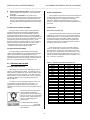
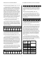
IOS-409
24-Channel Differential Digital I/O Board
USER’S MANUAL
ACROMAG INCORPORATED
30765 South Wixom Road
P.O. BOX 437
Wixom, MI 48393-7037 U.S.A.
[email protected]
Copyright 2009, Acromag, Inc., Printed in the USA.
Data and specifications are subject to change without notice.
Tel: (248) 295-0310
Fax: (248) 624-9234
8500-844-B11C007
SERIES IOS-409 I/O SERVER MODULE
24-CHANNEL DIFFERENTIAL DIGITAL I/O MODULE
___________________________________________________________________________________________
The information contained in this manual is subject to change
without notice. Acromag, Inc. makes no warranty of any kind with
regard to this material, including, but not limited to, the implied
warranties of merchantability and fitness for a particular purpose.
Further, Acromag, Inc. assumes no responsibility for any errors
that may appear in this manual and makes no commitment to
update, or keep current, the information contained in this manual.
No part of this manual may be copied or reproduced in any form,
without the prior written consent of Acromag, Inc.
Table of Contents
1.0 GENERAL INFORMATION...........................................
KEY IOS-409 FEATURES.............................................
I/O SERVER MODULE SOFTWARE LIBRARY...........
2.0 PREPARATION FOR USE............................................
UNPACKING AND INSPECTION..................................
BOARD CONFIGURATION...........................................
CONNECTORS.............................................................
IOS Field I/O Connector (P2).....................................
I/O Noise and Grounding Considerations..................
3.0 PROGRAMMING INFORMATION.................................
ADDRESS MAPS..........................................................
Control Register............................…………………....
Input/Output Channel Registers................................
Direction Control Registers........................................
Interrupt Enable Register………………………………
Interrupt Type Configuration Register........................
Interrupt Status Register................................…........
Interrupt Polarity Register..........................................
Interrupt Vector Register..........................…..............
IOS Identification Space............................................
IOS-409 PROGRAMMING CONSIDERATIONS............
I/O Handshake Operation………………………….…..
Programming Interrupts.....................................…....
4.0 THEORY OF OPERATION...........................................
FIELD INPUT/OUTPUT SIGNALS.................................
EIA-RS485 AND RS422 SERIAL INTERFACE…….…..
5.0 SERVICE AND REPAIR................................................
SERVICE AND REPAIR ASSISTANCE........................
PRELIMINARY SERVICE PROCEDURE......................
6.0 SPECIFICATIONS.........................................................
PHYSICAL……………………........................................
ENVIRONMENTAL........................................................
EIA-RS485/RS422 TRANSCEIVERS............................
Page
2
2
3
3
3
3
3
3
4
4
4
5
5
5
5
6
6
6
6
6
7
7
8
9
9
9
9
9
9
10
10
10
10
DRAWINGS
IOS-409 BLOCK DIAGRAM................…..........
IOS-409 EXAMPLE I/O CONNECTIONS……..
IOS-409 TERMINATION RESISTOR LOCATION……
Page
11
12
13
IMPORTANT SAFETY CONSIDERATIONS
It is very important for the user to consider the possible adverse
effects of power, wiring, component, sensor, or software failures
in designing any type of control or monitoring system. This is
especially important where economic property loss or human life
is involved. It is important that the user employ satisfactory
overall system design. It is agreed between the Buyer and
Acromag, that this is the Buyer's responsibility.
-2-
1.0 GENERAL INFORMATION
The I/O Server Module (IOS) Series IOS-409 module is a 24channel differential digital input/output board with interrupts. This
model allows channels to be programmed as input or output on a
bit basis, in any combination up to 24 channels. All channels can
be programmed to generate Change-Of-State (COS), Low, or
High level transition interrupts.
Each channel uses a robust RS485/RS422 transceiver which
permits half duplex bi-directional data transfer (one direction at a
time). The use of differential data transmission allows reliable
transmission of data at high rates over up to 4000 meter
distances and through noisy environments. Differential
transmission nullifies the effects of ground shifts and noise
signals which appear as common-mode voltages on the line.
The IOS-409 model temperature range is (-40 C to +85 C).
Four units mounted on a carrier board provide up to 96 I/O
points per 6U-VMEbus system slot. Since each channel can be
independently programmed as an input or output, loopback
monitoring is possible. A channel programmed as an input can
be used to monitor another channel programmed as an output.
The IOS-409 utilizes state of the art Surface-Mounted
Technology (SMT) to achieve its high channel density and is an
ideal choice for a wide range of industrial control and monitor
applications that require high-density, high-reliability, and highperformance at a low cost.
Important Note: The following IOS model are accessories to the
IOS Server Models: IOS-7200, IOS-7200-WIN, IOS-7400, and
IOS-7400-WIN; which are cULus Listed. This equipment is
suitable for use in Class I, Division 2, Groups A, B, C, and D or
non-hazardous locations only.
KEY IOS-409 FEATURES
High Channel Count - Interfaces with up to 24 input/output
points. Four units mounted on a carrier board provide up to
96 input and/or output channels in a single system slot.
Input and output channels may be intermixed in any
combination. The input circuitry of a single channel can also
be used to monitor the output state of a different channel to
efficiently implement “loopback” output control.
Long Distance Data Transmission - Data transmission
with up to 32 nodes and up to 4000 feet is possible.
Robust RS485/RS422 Transceivers - The IOS-409 is
designed for electrically harsh environments. All differential
I/O channels are protected against electrostatic discharge
(ESD), electrical fast transient (EFT), and electromagnetic
interference (EMI).
Programmable Change-of-State/Level Interrupts Interrupts are software programmable for any bit Change-OfState or Level on an individual channel basis.
Socketed Termination Resistors - The network termination
resistors are installed in sockets on the board and may be
easily inserted or removed as required.
No Configuration Jumpers or Switches - All configuration
is performed through software commands with no internal
jumpers to configure or switches to set.
Power Up & System Reset is Failsafe - For safety, all
channels are configured as input upon power-up and after a
system reset.
SERIES IOS-409 I/O SERVER MODULE
24-CHANNEL DIFFERENTIAL DIGITAL I/O MODULE
__________________________________________________________________________________________
Output Channels With Read Back - The differential output
channel registers can be read back to verify programmed
logic levels.
Conduction Cooled Module - I/O modules employ
advanced thermal technologies. A thermal pad and module
cover wicks heat away from the module and transfers the
energy to a heat spreading friction plate. Heat moves to the
enclosure walls where it is dissipated by the external cooling
fins.
BOARD CONFIGURATION
Power should be removed from the board when installing IOS
modules, cables, termination panels, and field wiring. Refer to
the following discussion for configuration and assembly
instructions. Model IOS-409 I/O Boards have no jumpers or
switches to configure--interrupts are configured through software
commands.
IOS MODULE Win32 DRIVER SOFTWARE
CONNECTORS
Acromag provides a software product (sold separately) to
facilitate the development of Windows Embedded Standard
applications interfacing with I/O Server Modules installed on
Acromag Industrial I/O Server systems. This software (Model
IOSSW-DEV-WIN) consists of a low-level driver and Windows 32
Dynamic Link Libraries (DLLS) that are compatible with a number
of programming environments including Visual C++, Visual
Basic.NET, Borland C++ Builder and others. The DLL functions
provide a high-level interface to the IOS carrier and modules
eliminating the need to perform low-level reads/writes of
registers, and the writing of interrupt handlers.
IOS Field I/O Connector (P2)
P2 provides the field I/O interface connector for mating IOS
modules to the carrier board. P2 is a 50-pin female receptacle
header (AMP 173279-3 or equivalent) which mates to the male
connector of the carrier board (AMP 173280-3 or equivalent).
This provides excellent connection integrity and utilizes goldplating in the mating area. The field and logic side connectors
are keyed to avoid incorrect assembly.
P2 pin assignments are unique to each IOS model (see
Table 2.1) and normally correspond to the pin numbers of the
field-I/O interface connector on the carrier board (you should
verify this for your carrier board). When reading Table 2.1 note
that channel designations are abbreviated to save space. For
example, channel 0 is abbreviated as I/O00+ and I/O00- for the +
and - connections, respectively.
IOS MODULE LINUX SOFTWARE
Acromag provides a software product (sold separately)
consisting of Linux software. This software (Model IOSSW-APILNX) is composed of Linux libraries designed to support
applications accessing I/O Server Modules installed on Acromag
Industrial I/O Server systems The software is implemented as a
library of “C” functions which link with existing user code
Table 2.1: IOS-409 Field I/O Pin Connections (P2)
2.0 PREPARATION FOR USE
Pin Description
I/O00+
I/O00I/O01+
I/O01I/O02+
I/O02I/O03+
I/O03I/O04+
I/O04I/O05+
I/O05I/O06+
I/O06I/O07+
I/O07I/O08+
I/O08I/O09+
I/O09I/O10+
I/O10I/O11+
I/O11I/O12+
UNPACKING AND INSPECTION
Upon receipt of this product, inspect the shipping carton for
evidence of mishandling during transit. If the shipping carton is
badly damaged or water stained, request that the carrier's agent
be present when the carton is opened. If the carrier's agent is
absent when the carton is opened and the contents of the carton
are damaged, keep the carton and packing material for the
agent's inspection.
For repairs to a product damaged in shipment, refer to the
Acromag Service Policy to obtain return instructions. It is
suggested that salvageable shipping cartons and packing
material be saved for future use in the event the product must be
shipped.
This board is physically protected with
packing material and electrically
protected with an anti static bag during
shipment. However, it is recommended
that the board be visually inspected for
evidence of mishandling prior to
applying power.
The board utilizes static sensitive
components
and should only be handled at a staticsafe workstation.
-3-
Number
1
2
3
4
5
6
7
8
9
10
11
12
13
14
15
16
17
18
19
20
21
22
23
24
25
Pin Description
I/O12I/O13+
I/O13I/O14+
I/O14I/O15+
I/O15I/O16+
I/O16I/O17+
I/O17I/O18+
I/O18I/O19+
I/O19I/O20+
I/O20I/O21+
I/O21I/O22+
I/O22I/O23+
I/O23RESERVED
GND
Number
26
27
28
29
30
31
32
33
34
35
36
37
38
39
40
41
42
43
44
45
46
47
48
49
50
SERIES IOS-409 I/O SERVER MODULE
24-CHANNEL DIFFERENTIAL DIGITAL I/O MODULE
__________________________________________________________________________________________
Table 3.1: IOS-409 I/O Space Address (Hex) Memory Map
HIGH
LOW
Base
HIGH Byte
LOW Byte
Base
Addr.+
D15
D08
D07
D00 Addr.+
01
Control Register
00
03
Input/Output
Input/Output
Channel Reg B
Channel Reg A
CH15
CH08
CH07
CH00 02
05
Input/Output
Not Used2
Channel Reg C
CH23
CH16 04
07
Direction Control
Direction Control
Register B
Register A
CH15
CH08
CH07
CH00 06
09
Direction Control
Not Used2
Register C
CH23
CH16 08
0B
R/W - Interrupt
R/W - Interrupt
Enable Register B
Enable Register A
CH15
CH08
CH07
CH00 0A
0D
R/W - Interrupt
Not Used2
Enable Register C
CH23
CH16 0C
0F
R/W - Interrupt
R/W - Interrupt
Type Register B
Type Register A
CH15
CH08
CH07
CH00 0E
11
R/W - Interrupt
Not Used2
Type Register C
CH23
CH16 10
13
R/W - Interrupt
R/W - Interrupt
Status Register B
Status Register A
CH15
CH08
CH07
CH00 12
15
R/W - Interrupt
Not Used2
Status Register C
CH23
CH16 14
17
R/W - Interrupt
R/W - Interrupt
Polarity Register B
Polarity Register A
CH15
CH08
CH07
CH00 16
19
R/W - Interrupt
Not Used2
Polarity Register C
CH23
CH16 18
1B
R/W - Interrupt
Not Used2
Vector Register1
1A
1D
1C
NOT USED2
7F
7E
I/O Noise and Grounding Considerations
The IOS-409 is non-isolated between the logic and field I/O
grounds since output common is electrically connected to the IOS
module ground. Consequently, the field I/O connections are not
isolated from the carrier board and backplane. Two ounce
copper ground plane foil has been employed in the design of this
model to help minimize the effects of ground bounce, impedance
drops, and switching transients. However, care should be taken
in designing installations without isolation to avoid noise pickup
and ground loops caused by multiple ground connections.
To minimize high levels of EMI the signal ground connection
at the field I/O port (pin 50) should be used to provide a path for
induced common-mode noise and currents. The ground path
provides a low-impedance path to reduce emissions.
EIA RS485/RS422 communication distances are generally
limited to less than 4000 feet. To minimize transmission-line
problems, all nodes connected to the cable must use minimum
stub length connections. The optimal configuration for the
RS485/RS422 bus is a daisy-chain connection from node 1 to
node 2 to node 3 to node n. The bus must form a single
continuous path, and the nodes in the middle of the bus must not
be at the ends of long branches, spokes, or stubs. See IOS-409
Example I/O Connections for example connection and
termination practices.
Transmission line signal reflections can be minimized with
proper termination. The EIA RS485/RS422 standard allows up to
32 driver/receivers to be connected to a single bus. Termination
resistors should only be used at the two extreme ends of the bus
and not at each of the nodes of the bus.
3.0 PROGRAMMING INFORMATION
ADDRESS MAPS
This board is addressable in the I/O Server Module space to
control the data transfer, and steering logic of the 24 EIA
RS485/RS422 serial ports. The I/O space may be as large as
64, 16-bit words (128 bytes) using address lines A1..A6, but the
IOS-409 only uses a portion of this space. The I/O space
address map for the IOS-409 is shown in Table 3.1.
Notes (Table 3.1):
1. The upper 8 bits (even byte) of this register are not driven
upon on interrupt select cycle. Pullups on the carrier board
data bus will cause these bits to always read high (1‟s).
2. The IOS will respond to addresses that are "Not Used" with
an active IOS module acknowledge ACK~. Data read at “Not
Used” addresses will be driven low.
The base address for the IOS module I/O space (see your
carrier board instructions) must be added to the addresses shown
in Table 3.1 to properly access the I/O space. Accesses can be
performed on an 8-bit (D08[EO]), or 16-bit (D16) word basis.
-4-
SERIES IOS-409 I/O SERVER MODULE
24-CHANNEL DIFFERENTIAL DIGITAL I/O MODULE
__________________________________________________________________________________________
the corresponding input channel to generate an interrupt. Only
those channels configured as inputs can generate interrupts.
Control Register (Write) - (Base + 00H)
This read/write register is used to issue a software reset. Bit0 when set to a logic high will perform a software reset. When
read this register will return random values.
The Interrupt Enable register at the carrier‟s base address +
offset 0A is used to control channels 00 through 07. For
example, channel 00 is controlled via data bit-0 as seen in the
table below. Registers for Channels 15 to 08 and Channels 23 to
16 are accessed similarly at offsets 0B and 0C hex, respectively.
Input/Output Channel Registers
(Read/Write) - (Base + 02, 03, 04)
Twenty-four possible input/output channels numbered 0
through 23 may be individually accessed via these registers. The
Input/Output Channel registers are used to monitor/read or
set/write channels 0 through 23. Channels 7 to 0 are accessed at
the carrier base address +02 via data bits 7 to 0. Channels 15 to
8 are accessed at the carrier base address +03 via data bits 15 to
8. Channels 23 to 16 are accessed at carrier base address + 04
via data bits 7 to 0.
Interrupt Enable Register
MSB
Data
Bit
07
Ch07
Data
Bit
07
Ch07
Data
Bit
15
Ch15
Data
Bit
07
Ch23
Data
Bit
05
Ch05
Data
Bit
04
Ch04
Data
Bit
03
Ch03
Data
Bit
02
Ch02
Data
Bit
01
Ch01
LSB
Data
Bit
00
Ch00
Channel read operations use 8-bit, or 16-bit data transfers.
The upper 8 bits of register C are “Not Used” and will always read
low (0‟s) for D16 accesses.
The table below shows all channels and their corresponding
I/O data bit.
Input/Output Channel 7 to 0 Register
Data
Data
Data
Data
Data
Data
Bit
Bit
Bit
Bit
Bit
Bit
06
05
04
03
02
01
Ch06 Ch05 Ch04
Ch03
Ch02
Ch01
Input/Output Channel 15 to 8 Register
Data
Data
Data
Data
Data
Data
Bit
Bit
Bit
Bit
Bit
Bit
14
13
12
11
10
09
Ch14 Ch13 Ch12
Ch11
Ch10
Ch09
Input/Output Channel 23 to 16 Register
Data
Data
Data
Data
Data
Data
Bit
Bit
Bit
Bit
Bit
Bit
06
05
04
03
02
01
Ch22 Ch21 Ch20
Ch19
Ch18
Ch17
Data
Bit
06
Ch06
All input channel interrupts are disabled (set to “0”) following
a power-on or software reset.
Data
Bit
00
Ch00
Interrupt Type (COS or H/L) Configuration Registers
(Read/Write) - (Base + 0E, 0F, 10)
The Interrupt Type Configuration Registers determine the
type of input channel transition that will generate an interrupt for
each of the 24 possible interrupting channels. A “0” bit selects
interrupt on level. An interrupt will be generated when the input
channel level specified by the Interrupt Polarity Register occurs
(i.e. Low or High level transition interrupt). A “1” bit means the
interrupt will occur when a Change-Of-State (COS) occurs at the
corresponding input channel (i.e. any state transition, low to high
or high to low).
Data
Bit
08
Ch08
Data
Bit
00
Ch16
The Interrupt Type Configuration register at the carrier‟s base
address + offset 0E is used to control channels 00 through 07.
For example, channel 00 is controlled via data bit-0 as seen in
the table below. Registers for Channels 15 to 08 and Channels
23 to 16 are accessed similarly at offsets 0F and 10 hex,
respectively.
Channel read/write operations use 8-bit, or 16-bit data
transfers with the lower ordered bits corresponding to the lowernumbered channels for the register of interest. All input/output
channels are configured as inputs on a power-on or software
reset. The unused upper 8 bits of register C are “Not Used” and
will always read low (0‟s) for D16 accesses.
Interrupt Type (COS or H/L) Configuration Register
MSB
Data
Bit
07
Ch07
Direction Control Registers (Read/Write) - (Base + 06, 07, 08)
The data direction (input or output) of the 24 differential
channels is selected via these registers. The data direction of
each channel can be independently set on a bit by bit basis.
Setting a bit high configures the corresponding channel data
direction for output. Setting the control bit low configures the
corresponding channel data direction for input.
Data
Bit
06
Ch06
Data
Bit
05
Ch05
Data
Bit
04
Ch04
Data
Bit
03
Ch03
Data
Bit
02
Ch02
Data
Bit
01
Ch01
LSB
Data
Bit
00
Ch00
Channel read or write operations use 8-bit, or 16-bit data
transfers. The upper 8 bits of register C are “Not Used” and will
always read low (0‟s) for D16 accesses. Note that interrupts will
not occur unless they are enabled.
The default power-up state of these registers is logic low.
Thus, all channels are configured as inputs on system reset or
power-up. The unused upper byte of register C is “Not Used” and
will always read low (0‟s).
All bits are set to “0” following a reset which means that, if
enabled, the inputs will cause interrupts for the levels specified by
the digital input channel Interrupt Polarity Register.
Interrupt Enable Registers (Read/Write) - (Base + 0A, 0B, 0C)
The Interrupt Enable Registers provide a mask bit for each of
the 24 channels. A “0” bit will prevent the corresponding input
channel from generating an external interrupt. A “1” bit will allow
-5-
SERIES IOS-409 I/O SERVER MODULE
24-CHANNEL DIFFERENTIAL DIGITAL I/O MODULE
__________________________________________________________________________________________
Interrupt Status Registers (Read/Write) - (Base + 12, 13, 14)
Ch07
The Interrupt Status Register reflects the status of each of
the interrupting channels. A “1” bit indicates that an interrupt is
pending for the corresponding channel. A channel that does not
have interrupts enabled will never set its interrupt status flag. A
channel‟s interrupt can be cleared by writing a “1” to its bit
position in the Interrupt Status Register (writing a “1” acts as a
reset signal to clear the set state). This is known as the “Release
On Register Access” (RORA) method, as defined in the VME
system architecture specification. However, if the condition which
caused the interrupt to occur remains, the interrupt will be
generated again (unless disabled via the Interrupt Enable
Register). In addition, an interrupt will be generated if any of the
channels enabled for interrupt have an interrupt pending (i.e. one
that has not been cleared). Writing “0” to a bit location has no
effect; that is, a pending interrupt will remain pending.
Data
Bit
04
Ch04
Data
Bit
03
Ch03
Data
Bit
02
Ch02
Data
Bit
01
Ch01
Ch03
Ch02
Ch01
Ch00
The Interrupt Vector Register maintains an 8-bit interrupt
pointer for all channels configured as input channels. The Vector
Register can be written with an 8-bit interrupt vector. This vector
is provided to the carrier and system bus upon an active INTSEL*
cycle. Reading or writing to this register is possible via 16-bit or
8-bit data transfers.
Interrupt Vector Register
MSB
07
06
05
04
03
02
01
LSB
00
Interrupts are released on register access to the Interrupt
Status register. Issue of a software or hardware reset will clear
the contents of this register to 0.
IOS Identification Space (Read Only, 32 evenbyte addresses)
Each IOS module contains identification (ID) information that
resides in the ID space per the IOS module specification. This
area of memory contains 32 bytes of information at most. Both
fixed and variable information may be present within the ID
space. Fixed information includes the "IOS" identifier, model
number, and manufacturer's identification codes. Variable
information includes unique information required for the module.
The IOS-409 ID Space does not contain any variable (e.g. unique
calibration) information. ID Space bytes are addressed using
only the odd addresses in a 64 byte block (on the “Big Endian”
VMEbus). Even addresses are used on the “Little Endian” PC
ISA or PCI buses.
Interrupt Status Register
Data
Bit
05
Ch05
Ch04
Interrupt Vector Register (Read/Write) - (Base + 1A)
The Interrupt Status register at the carrier‟s base address +
offset 12 is used to monitor pending interrupts corresponding to
channels 00 through 07. For example, channel 00 is monitored
via data bit-0 as seen in the table below. Registers for Channels
15 to 08 and Channels 23 to 16 are accessed similarly at offsets
13 and 14 hex, respectively.
Data
Bit
06
Ch06
Ch05
The upper 8 bits of register C are “Not Used” and will always
read low (0‟s) for D16 accesses. All bits are set to “0” following a
reset which means that the inputs will cause interrupts when they
are below TTL threshold (provided they are enabled for interrupt
on level).
Note that interrupts are not prioritized via hardware. The
system software must handle interrupt prioritization.
MSB
Data
Bit
07
Ch07
Ch06
LSB
Data
Bit
00
Ch00
The unused upper 8 bits of register C are “Not Used” and will
always read low (0‟s) for D16 accesses. All bits are set to “0”
following a reset which means that all interrupts are cleared.
Interrupt Polarity Registers (Read/Write) - (Base + 16, 17, 18)
The IOS-409 ID Space contents are shown in Table 3.2.
Note that the base-address for the IOS module ID space (see
your carrier board instructions) must be added to the addresses
shown to properly access the ID information. Execution of an ID
Space Read operation requires 0 wait states.
The Interrupt Polarity Register determines the level that will
cause a channel interrupt to occur for each of the channels
enabled for level interrupts. A “0” bit specifies that an interrupt
will occur when the corresponding input channel is low (i.e. a “0”
in the digital input channel data register). A “1” bit means that an
interrupt will occur when the input channel is high (i.e. a “1” in the
digital input channel data register). Note that no interrupts will
occur unless they are enabled by the Interrupt Enable Register.
Further, the Interrupt Polarity Register will have no effect if the
Change-of-State (COS) interrupt type is configured by the
Interrupt Type Configuration Register.
Table 3.2: IOS-409 ID Space Identification (ID)
Hex Offset
From ID
Numeric
Base
Value
Address
(Hex)
Field Description
00
49
02
50
04
41
06
43
08
A3
Acromag ID Code
0A
20
IOS Model Code1
0C
00
Not Used
(Revision)
0E
00
Reserved
10
00
Not Used
12
00
Not Used
14
0C
Total Number of
ID PROM Bytes
16
B6
CRC
The Interrupt Polarity register at the carriers base address +
offset 16 is used to control channels 00 through 07. For example,
channel 00 is controlled via data bit-0 as seen in the table below.
Registers for Channels 15 to 8 and Channels 23 to 16 are
accessed similarly at offsets 17 and 18 hex, respectively.
Interrupt Polarity Register
MSB
Data
Bit
07
Data
Bit
06
Data
Bit
05
Data
Bit
04
Data
Bit
03
Data
Bit
02
Data
Bit
01
LSB
Data
Bit
00
-6-
SERIES IOS-409 I/O SERVER MODULE
24-CHANNEL DIFFERENTIAL DIGITAL I/O MODULE
__________________________________________________________________________________________
18 to 3E
yy
Not Used
The following step-by-step sequence gives an example of
how data could be transferred from IOS-409A to IOS module
IOS-409B.
Notes (Table 3.2):
1. The IOS model number is represented by a two-digit code
within the ID space (the IOS-409 model is represented by 20
Hex).
1. IOS-409B drives channel 16 (Ready For Data signal) to
an active high state. This indicates to the IOS-409A that
the IOS-409B is ready to receive data. The IOS-409A
drives channel 17 (Output Data Valid~) inactive to a high
state.
2. IOS-409A receives channel 16 (Ready For Data signal)
as active high. This indicates to the IOS-409A that the
IOS-409B is ready to receive new data.
3. IOS-409A drives valid data on channels 0 to 15 and
drives channel 17 (Output Data Valid~) active to a low
state.
4. IOS-409B receives channel 17 (Input Data Valid~) active
low. IOS-409B drives channel 16 (Ready For Data) low,
indicating that input register is full and is not ready for
new data.
5. IOS-409B reads the new data from it‟s input register and
then drives channel 16 (Ready For Data) high.
IOS-409 PROGRAMMING CONSIDERATIONS
To make programming and communicating with the board
easier, Acromag provides you with the I/O Server Module
Software Library diskette. The functions provided are written in
the “C” programming language and can be linked into your
application. Refer to the “README.TXT” file in the root directory
and the “INFO409.TXT” file in the “IOS-409” subdirectory on the
diskette for details.
Acromag also provides a software diskette of IOS module
Object Linking and Embedding (OLE) drivers for Windows 95
and Windows NT compatible application programs (Model
IOSSW-OLE-PCI, MSDOS format). This software provides
individual drivers that allow all IOS modules and the APC8620
carrier to be easily integrated into Windows application
programs, such as Visual C++ , Visual Basic , Borland
Delphi , Microsoft Office 97 applications and others. The
OLE controls provide a high-level interface to IOS modules,
eliminating the need to perform low-level reads/writes of
registers, and the writing of interrupt handlers—all the
complicated details of programming are handled by the OLE
controls. These functions are intended for use in conjunction with
an Acromag personal computer carrier and consist of a carrier
OLE control, and an OLE control for each Acromag IOS module
as well as a generic OLE control for non-Acromag IOS modules.
Steps 1-5 would be repeated to transfer additional data.
In addition, channel 17 could be programmed at the IOS409B to generate an interrupt upon a change of state to logic low.
The interrupt service routine could set channel 16 low and read
the input data register. After the data is read, the interrupt
service routine could set channel 16 high to inform IOS-409A it is
ready for new data.
Programming Interrupts
Digital input channels can be programmed to generate
interrupts for the following conditions:
I/O Handshake Operation
Change-of-State (COS) at selected input channels.
Input level (polarity) match at selected input channels.
The IOS-409 has 24 channels that can be independently
configured as input or output ports. With independent
configuration of channels the IOS-409 can be used to move data
in either direction on a word-by-word basis. The data word size
can be any number of user defined bits up to the 24 channels,
minus the number of handshake channels used.
Interrupts generated by the IOS-409 use interrupt request line
INTREQ0* (Interrupt Request 0). The interrupt release
mechanism employed is the Release On Register Access
(RORA) type. This means that the interrupter will release the I/O
Server Module interrupt request line (INTREQ0) after all pending
interrupts have been cleared by writing a “1” to the appropriate bit
positions in the input channel Interrupt Status Register.
Channels not used to move data can be defined as
handshake signals. The handshake channels can consist of
status input lines and control output lines.
The Interrupt Vector Register contains a pointer vector to an
interrupt handling routine. One interrupt handling routine must be
used to service all possible channel interrupts.
There are a number of different handshake protocols
available. For example; two directly connected IOS-409 modules
could transfer 16-bit data from IOS-409A to IOS-409B. The IOS409B will acknowledge the transfer.
When using interrupts, input channel bandwidth should be
limited to reduce the possibility of missing channel interrupts. For
a given input channel, this could happen if multiple changes
occur before the channel‟s interrupt is serviced. The response
time of the input channels should also be considered when
calculating this bandwidth. The total response time is the sum of
the input buffer response time, plus the interrupt logic circuit
response time, and this time must pass before another interrupt
condition will be recognized. The Interrupt Input Response Time
is specified in section 6.
For example, IOS-409A has channels 0 to 15 configured as
outputs. Channel 16 is configured as input handshake signal
(Ready For Data). Channel 17 is configured as output
handshake signal (Output Data Valid~).
The IOS-409B has channels 0 to 15 configured as inputs.
Channel 16 is configured as output handshake signal (Ready For
Data). Channel 17 is configured as input handshake signal (Input
Data Valid~).
-7-
SERIES IOS-409 I/O SERVER MODULE
24-CHANNEL DIFFERENTIAL DIGITAL I/O MODULE
__________________________________________________________________________________________
recorded in the carrier board‟s Interrupt Pending Register and
passed to the PCI bus by driving interrupt request signal INTA#
active.
3. The host processor uses the PCI interrupt to locate an interrupt
service routine to process interrupts from the carrier board.
4. The carrier board interrupt service routine examines the
carrier board‟s Interrupt Pending Register and invokes IOS
module interrupt service routines to service individual IOS
modules.
3. The carrier board interrupt service routine accesses the
interrupt space of the IOS module selected to be serviced.
Note that the interrupt space accessed must correspond to
the interrupt request signal driven by the IOS module.
4. The carrier board will assert the INTSEL* signal to the
appropriate IOS module together with (carrier board generated)
address bit A1 to select which interrupt request is being
processed (A1 low corresponds to INTREQ0*; A1 high
corresponds to INTREQ1*).
5. The IOS module receives an active INTSEL* signal from the
carrier and supplies its interrupt vector to the host processor
during this interrupt acknowledge cycle. An IOS module
designed to release its interrupt request on acknowledge will
release its interrupt request upon receiving an active
INTSEL* signal from the carrier. If the IOS module is
designed to release it‟s interrupt request on register access
the interrupt service routine must also access the required
register to clear the interrupt request.
6. If the IOS module interrupt stimulus has been removed and
no other IOS modules have interrupts pending, the interrupt cycle
is completed (i.e. the carrier board negates its interrupt request
INTA#).
Interrupt Programming Example
1. Clear the Interrupt Enable Bits in the Carrier Board Status
Register by writing a "0" to bit 2 and bit 3.
2. Perform Specific IOS-409 Module Programming - see the
Change-of- State or Level (Polarity) Match programming
examples
that follow, as required for your application.
3. Write a “1” to bit 2 of the Carrier Status/Control Register
Module
Interrupt Enable bit to enable IOS module interrupts to the PCI
bus.
Programming Example for Change-of-State Interrupts:
1. Select channel Change-of-State interrupts by writing a “1” to
each channel‟s respective bit in the Interrupt Type Register.
Note that Change-Of-State interrupts (specified with “1”) may be
mixed with polarity match interrupts (specified with “0”).
3. Enable individual input channel interrupts by writing a “1” to
each channel‟s respective bit in the Interrupt Enable Register.
4. Clear pending interrupts by writing a “1” to each channel‟s
respective bit in the Interrupt Status Register.
Change-of-State Interrupts may now be generated by the input
channels programmed above for any Change-Of-State
transition.
Processing Change-of-State Interrupts:
1. Clear the interrupting channel(s) by writing a “1” to the
appropriate bits in the IOS-409 Interrupt Status Register.
Programming Example for Level (Polarity) Match Interrupts:
4.0 THEORY OF OPERATION
1. Select channel Polarity Match Interrupts by writing a “0” to
each
channel‟s respective bit in the Interrupt Type Register. Note that
Change-Of-State interrupts (specified with “1”) may be mixed
with Polarity Match Interrupts (specified with “0”).
3. Select the desired polarity (High/Low) level for interrupts by
writing a “0” (Low), or “1” (High) level to each channel‟s
respective bit in the Interrupt Polarity Register.
4. Enable individual input channel interrupts by writing a “1” to
each channel‟s respective bit in the Interrupt Enable Register.
5. Clear pending interrupts by writing a “1” to each channel‟s
respective bit in the Interrupt Status Register.
Interrupts can now be generated by matching the input level with
the selected polarity for programmed interrupt channels.
This section describes the basic functionality of the circuitry
used on the board. Refer to the IOS-409 Block Diagram as you
review this material.
FIELD INPUT/OUTPUT SIGNALS
The field I/O interface to the IOS module is provided through
connector P2 (refer to Table 2.1). These pins are tied to the
inputs and outputs of EIA RS485/RS422 line transceivers.
Signals received are converted from the required EIA
RS485/RS422 voltages signals to the TTL levels required by the
Field Programmable Gate Array (FPGA). Likewise TTL signals
are converted to the EIA RS485/RS422 voltages for data output
transmission. The Field Programmable Gate Array provides the
necessary interface to the RS485/RS422 transceivers for control
of data output or input and monitoring of input signals for
generation of interrupts, if enabled.
Processing Level (Polarity) Match Interrupts:
1. Disable the interrupting channel(s) by writing a “0” to the
appropriate bits in the IOS-409 Interrupt Enable Register.
2. After the interrupt stimulus has been removed, clear
the interrupting channel(s) by writing a “1” to the
appropriate bits in the IOS-409 Interrupt Status Register.
If the input stimulus is still applied, this will not clear
the Interrupt Status Register bit and the interrupting
channel(s) must remain disabled until the interrupt
stimulus has been removed. After removal of the input
stimulus the channel(s) may be cleared and re-enabled.
3. Re-enable the interrupting channel(s) by writing a “1” to
the appropriate bits in the Interrupt Enable Register.
The field I/O interface to the carrier board is provided through
connector P2 (refer to Table 2.1). Field I/O points are NONISOLATED. This means that the field return and logic common
have a direct electrical connection to each other. As such, care
must be taken to avoid ground loops (see Section 2 for
connection recommendations). Ignoring this effect may cause
operational errors, and with extreme abuse, possible circuit
damage.
General Sequence of Events for Processing an Interrupt
Interrupt Operation
1. The IOS-409 asserts the Interrupt Request 0 Line (INTREQ0*)
in response to an interrupt condition at one or more inputs.
2. A generated interrupt is recognized by the carrier board and is
Digital input channels of this model can be configured to
generate interrupts for Change-Of-State (COS) and input level
(polarity) match conditions at enabled inputs. An 8-bit interrupt
-8-
SERIES IOS-409 I/O SERVER MODULE
24-CHANNEL DIFFERENTIAL DIGITAL I/O MODULE
__________________________________________________________________________________________
service routine vector is provided during interrupt acknowledge
cycles on data lines D0...D7. The interrupt release mechanism
employed is RORA (Release On Register Access).
PRELIMINARY SERVICE PROCEDURE
Before beginning repair, be sure that all of the procedures in
Section 2, Preparation For Use, have been followed. Also, refer
to the documentation of your carrier board to verify that it is
correctly configured. Replacement of the module with one that is
known to work correctly is a good technique to isolate a faulty
module.
Fail-Safe Operation
The IOS-409 operation is considered „Fail-safe‟. That is, the
input/output channels are always configured as input upon powerup reset, and a system software reset. This is done for safety
reasons to ensure reliable control of the output state under all
conditions.
CAUTION: POWER MUST BE TURNED OFF BEFORE
REMOVING OR INSERTING BOARDS
EIA-RS485 AND RS422 SERIAL INTERFACE
Acromag‟s Applications Engineers can provide further
technical assistance if required. When needed, complete repair
services are also available from Acromag.
The EIA-RS485 and RS422 interface specifies a balanced
driver with balanced receivers. Balanced data transmission
refers to the fact that two conductors are switched per signal and
the logical state of the data is referenced by the difference in
potential between the two conductors, not with respect to signal
ground. The differential method of data transmission makes EIARS485 and RS422 ideal for noisy environments since it
minimizes the effects of coupled noise and ground potential
differences. That is, since these effects are seen as commonmode voltages (common to both lines), not differential, they are
rejected by the receivers.
The EIA-RS422 standard defines a bus with a single driver
and multiple receivers.
The EIA-RS485 standard defines a bi-directional, terminated,
driver and receiver configuration. Half-duplex operation is
provided by the sharing of a single data path for transmit and
receive. The maximum data transmission cable length is
generally limited to 4000 feet without a signal repeater installed.
With respect to EIA-RS485 and RS422, logic states are
represented by differential voltages from 1.5 to 5V. The polarity
of the differential voltage determines the logical state. A logic “0”
is represented by a negative differential voltage between the
terminals (measured A to B, or + to -). A logic “1” is represented
by a positive differential voltage between the terminals (measured
A to B, or + to -). The line receivers convert these signals to the
conventional TTL level.
5.0 SERVICE AND REPAIR
SERVICE AND REPAIR ASSISTANCE
Surface-Mounted Technology (SMT) boards are generally
difficult to repair. It is highly recommended that a non-functioning
board be returned to Acromag for repair. The board can be easily
damaged unless special SMT repair and service tools are used.
Further, Acromag has automated test equipment that thoroughly
checks the performance of each board. When a board is first
produced and when any repair is made, it is tested, placed in a
burn-in room at elevated temperature, and retested before
shipment.
Please refer to Acromag's Service Policy Bulletin or contact
Acromag for complete details on how to obtain parts and repair.
-9-
SERIES IOS-409 I/O SERVER MODULE
24-CHANNEL DIFFERENTIAL DIGITAL I/O MODULE
__________________________________________________________________________________________
6.0 SPECIFICATIONS
PHYSICAL
EIA-RS485 TRANSCEIVERS
Physical Configuration…….…... Single I/O Server Module.
Length................................ 4.030 in. (102.36 mm).
Width.................................. 1.930 in. (49.02 mm).
Board Thickness................. 0.062 in. (1.59 mm).
Height......
0.500 in. (12.7 mm).
Channel Configuration……..…. 24 independent, non-isolated EIA
RS485/RS422 serial ports with a
common signal return
connection.
Data Rate……………….……… 250K bits/sec, Maximum.
Cable Length………………..…. 4000 feet, Maximum. Use of a
signal repeater can extend
transmission distances beyond
this limit.
Termination Resistors…………. 120 Termination Resistors
installed in sockets on board at
network end points only (see
IOS-409 Termination Resistor
Location)
Differential Output Voltage…… 5V Maximum; 1.5V Minimum
(with 27 load).
Common Mode Output
Voltage………………………….. 3V Maximum.
Output Short Circuit Current…. 250mA, Maximum.
Power:
Configured as Output with Termination Resistors Installed
+5 Volts ( 5%)..............….. 600mA, Typical
800mA Maximum.
Configured as Input
+5 Volts ( 5%)..............….. 20mA, Typical
30mA Maximum.
+/-12 Volts ( 5%) from P1.. 0mA (Not Used)
Maximum Vcc Rise Time.... 100m seconds
ENVIRONMENTAL
Operating Temperature.........… -40 C to +85 C.
Relative Humidity...................... 5-95% Non-Condensing.
Storage Temperature................ -55 C to +125 C.
Rise or Fall Time……….……… 250ns Minimum, 800ns Typical,
2000ns Maximum (RDIFF = 54 ,
CL =100pF).
Non-Isolated....................…...... Logic and field commons have a
direct electrical connection.
Resistance to RFI.........…......... Designed to comply with
IEC1000-4-3 Level 3 (10V/m at
frequencies o f 27MHz to
500MHz) and European Norm
EN50082-1.
Input Hysteresis……………..… 70mV (VCM=0V).
Interrupt Input Response
Time…………………………….. 500nS minimum to 2250nS
maximum, depending on when
the input transition occurs with
respect to the 8MHz clock.
Measured from input transition to
INTREQ0 line assertion.
Electromagnetic Interference
Immunity (EMI)…...…..….....…. No digital upset under the
influence of EMI from switching
solenoids, commutator motors,
and drill motors.
Electrostatic Discharge
Immunity (ESD)…....…..........… Complies with IEC1000-4-2 Level
1 (2KV direct contact discharge)
at field input/output terminals and
European Norm EN50082-1.
Surge Immunity………………… Not required for signal I/O per
European Norm EN50082-1.
Electric Fast Transient
Immunity EFT………………….. Complies with IEC1000-4-4 Level
2 (0.5KV at field input and output
terminals) and European Norm
EN50082-1.
Radiated Emissions………...... Meets or exceeds European
Norm EN50081-1 for class A
equipment.
Warning: This is a class A product. In a domestic environment
this product may cause radio interference in which the
user may be required to take adequate measures.
- 10 -
SERIES IOS-409 I/O SERVER MODULE
24-CHANNEL DIFFERENTIAL DIGITAL I/O MODULE
__________________________________________________________________________________________
- 11 -
SERIES IOS-409 I/O SERVER MODULE
24-CHANNEL DIFFERENTIAL DIGITAL I/O MODULE
__________________________________________________________________________________________
- 12 -
SERIES IOS-409 I/O SERVER MODULE
24-CHANNEL DIFFERENTIAL DIGITAL I/O MODULE
__________________________________________________________________________________________
- 13 -