1
CONTENT Challtcr I
1 N IHODliCTION
I- I
Chapter 2
GENERAL FEATURES
2-1
Specification
Processor
Ma t h Coprocessor
Mcmory Systcm
I/O Subsystem
System functions
Chapter 3
INSTALLING COMPONENTS
:2 - I
2-3
2-6
2-8
2- 11
2-12
3-1
Installing 80387SX Math Coprocessor
3-1
System Mcmory Configuration
3-3
Control or Systcm Spccd
Systcm Board Jumpcr Setting
3-8
3-10
S y s t c III Il () a r d Connectors
3-\ I
Chapter 4
TECHNICAL INFOI~MATION
Memory Mapping
I/O Address Map
System Timers
System Interrupts
Direct Memory Access (DMA)
Real Time Clock and CMOS RAM
CMOS RAM Address Map
Rea I Tim e C I 0 c kin for mat ion
System Expansion Bus
APPENDIX A
SYSTEM BIOS
Self-Test
System Setup
APPENDIX B
OPERATION & MAINTENANCE
Keepi ng the System Cool
Cleaning the "Golden Finger"
Cleaning the Motherboard
APPENDIX C
SYSTEM BOARD LAYOUT
4-1
4-1
4-2
4-4
4-6
4-7 4-9 4-10 4- I I 4-12 A-I
A-I A-4 B-1 B-2 B-2 B-3 C-l
Chapter 1
Introduction
The Panther-II system board is a high
performance system
board
that
represents a
significant
technological
advance
over
the
conventional
3S6SX
designs.
It
offers
an
increased power and flexibility architecture by
supporting S0386SX processor speeds up to 33 Mhz
(See NOTE Oil
pre/ace).
The design utilizes
advanced main frame techniques such as two or
fOllr way interlea\'ing along with high speed page
mode capability.
inexpensive
The
Panther-II
orfers
an
entrance to 3Sb-speciric applications. It combincs
the abilities of the 00386 and the S028b machines.
L ike a n 8 0 3 8 () III a chi II e, i t 1)1' 0 l' e sse sill S t rue t ion s
internally in 32-bit chunks.
Like an 80286
III a e h inc, it (l per ate s \V i t h a I () - bit d a tab usa n d a
24-bit address bus. This constructions allows the
Panther-II
s\'stem
to
rlln
30b
sortware
In
essentially a 2X6 hardware environment.
For the 1lll'I1l!HY S\<;(elll, It SlippurtS liP to I!J
MByte of DR.·\i\ls on the S)stc'lll buard.
System
and V ide 0 s had 0 \\' i n g rea I LI res are SliP P P I' ted 0 ~1 a II
16K bOll n dar i e s bel wee n () -4 (J K and 1M. I tis a I s ()
opt i III i zed t u a I I 0 \\ mix i 11 g 0 r [) R A 1\1 t yp cs log i \' e
end lIser the maximum flexibility in ehuosing the
correct memory capacit~ 1'01' their applications,
This flexibility in configuration allows you to
select an ideal cost/performance combination.
I-I
INTRODUCTION
\:
"
';;
~
:
The Pan ther-II is a fu II y P'C/ A T compa ti ble
~ystem dboahr.d
i mplemen t~dd h~ ihth
af
h j gh I Y
Integrate c IP sets to provl e Ig per ormance,
reliability and compatibilityl. ,It;·is;:based Ion the
386SX CPU which ca n access the· ,world's,da rgest
existing microcomputer software ,base" including
the growing 32-bit software. '. ";J ,f 1,:, ,,' ..
'l,;:'
J ...
To speed up the switching of CPU between
protected and real mode, a special feature known
as 'OS/2 Optimization' is alsorincorporated. Ifhis
provides an unique method to. handle; the,.modc
switching which will improve the performancelfor
advanced operating system and expanded memory
manager applications.
; \- ,:'-l1[1!~'1
':, i
I
, J'
~ <\
?r
!
1
f
f'.
J!,i'IRegarding to the issueoficompatibility,
Panther-II system is fully hardware)and,software
compatible with associated PC-AT pt;QduclS;, This
mea n s· ;t hat .. v i rt u ally a 11 i! the i; Lh !l.r d war e j ,I and
software'that.is available for thed)G/ A T!cant also
be run on, a ·system you build arou,n<!;;the IPa.nther-;
II system.! It,supports MS-DOS;! X-ep)x, \ Unixnand
all PC/AT application programs. Users can run
applications designed for the PC/AT onlPanther-ll
wi.thout any,· modification. "Multi.:...tasking I and
multhuser capabilities are fullYifunctional;on this
system board.
,)d ?:)jlr.~ 'ii"
~J I :,~
.. : ,
,~ ..
'~
'/1 1)
I i r:
t ~
J
!,:, '\ ; f:: /
t
';r!1",In
addition, ·the' rPanther"IId, provides
stand,a,r.dIISA expansion bus,:con~ectors, so that
add~on""cards ,developed for the, P.Gi'iAT,·,Will be
full y,/ functional. On - boa rd PPWe.r.;"good ,generator
is also implemented to ensure. the reliability of
the system and is capable of working with any
1-2
A,
•
INTRODUCTION
powcr supplies.
Panther-II is a perfect choice for CAD/CAM
worksta tion, file server and end user applications.
It is designed for the most advanccd computcr
based applications for today and in the futurc.
, i
1-3
INTRODUCTION
THIS PAGE IS INTENTIONALLY LEFT BLANK
1-4
Chapter 2
General Features
SPECIFICATION
l)rocessor Su IJsystclII :
Intel 80386SX CPU Optional 80387SX Co-processor Speed :
Turbo/normal speed Software/hardware selectable l\h'lIlory SUIJSystl'lIl :
16MB maximum lIsing 4M SIMMs 2MB using 256Kbx4 DRAM ~hips Page/Interleave memory: Page mode memory
2-way and 4-way interleave mode System BIOS shadow Video BIOS shadow Parity Check option 5I2K Eprom BIOS 2-1
GENERAL FEATURES
I/O Subsystem:
Compatible to standard AT bus Four 16-bit expansion slots Two 8-bi t expa nsion slots System Support Functions:
-
8-Channel DMA (Direct Memory Access)
16-level interrupt
3 programmable timers
CMOS RAM for system configuration
Real time clock with battery backup
OS/2 Optimization (Fast A20 gate and fast
reset)
Other Features:
On board POWERGOOD test circuit
External battery connector
Hardware turbo switch
2-2
la:NEHAL FEATUHES
PROCESSOR
The 80386SX Microprocessor is a 32-bit CPU
with a 16-bit external data bus and a 24-bit
external address bus. The 386SX CPU brings the
high-performance
software
of
the
Intel386
Architecture to mid-range systcms. It providcs thc
performance benefits of a 32-bit programming
architecture with the cost saving associated with
16-bit hardware systems.
The 386SX Microprocessor is 100% objcct
code compatible with the 386DX, 286 and 8086
microprocessors. [I provide 386))X bascd systcms
optimized for performance and 386SX CPU bascd
systems optimized ror cost. both sharing the same
operating
SYSICIIlS
and
application
SOfl\\'are.
lJ n I i k c the ::' i\ () - has cds \' sIc III sag a ins I \\' h i l' h i I
com pet c s , the .1 i\ (J S.\. i n her I I S I h e 3 X() , s pro tee I c d
and
virtual 8086 modes and
internal 32-bit
process In g.
Instruction pipeling. high bus bandwidth.
and a very high performance ,\LU ensure sllort
avcrage instruction cxecution timcs and high
system throughput. The 386SX CPU is capable or
execution at sllstained rales of 2.5-3.0 mi[lion
instructions per seculld.
The i n t e g rat e dIlle m l) I' : management unit
(MMU) includes an addrcss translalion cache.
a d van c e cI m u I t i - t ask i n g h a r d \\' arc. and a 0 u r - [eve I
hardware-enforccd
protection
mechanism
to
support operating systems.
The virtual machine
r
2-3
GENERAL FEATURES
capability of the 386SX CPU allows simultaneous
execution of applications from multiple operating
systems such as MS-DOS and UNIX.
80386SX is not only an enhanced version of
80286, but designed to overcome the deficiencies
of 80286.
It allows you to make use of
application software that a 286 just can't handle.
For example, a very important attribute of any
multi-tasking/multi-user operating system is its
ability to rapidly switch between tasks or
processes.
The 386SX Microprocessor directly
supports this operation by providing a task switch
instruction in hardware.
The 386SX Microprocessor has two modes of
operation: Real Address Mode (Real Mode), and
Protected Virtual Address Mode (Protected Mode).
Real Mode has the same base architecture as the
8086, but allows access to the 32-bit register set of
the 386SX Microprocessor.
The complete capabilities of the 386SX
Microprocessor are unlocked when the processor
operates In Protected Virtual Address Mode.
Protected Mode vastly increases the linear address
space to four gigabytes and allows the running of
virtual memory programs of almost unlimited size.
In addition, Protected Mode allows the 386SX
Microprocessor to run all of the existing 386DX
CPU, 80286 and 8086 CPU's software, while
providing a sophisticated memory management and
a
hardware-assisted
protection
mechanism.
Protected Mode allows the use of additional
instructions specially optimized for supporting
2-4
(J
multitasking ol)crating SystClll.
The 380SX Microprocessor also urrers ruur
levcls or protectiun
which are optimized to
support a multi-tasking opcrating systcm and to
isolate and protect user programs from each other
and the operating systelll.
2-5
GENERAL FEATURES
MATH COPROCESSOR
The demand for sophisticated, number
crunching scientific and business applications has
rapidly increased in recent years.
80386SX
features an integer Arithmetic Logic Unit which
only handles simple integer operations such as
addition and
multiplication.
Floating-point
operations
which
are
actually
utilized
by
applications
must
be
accomplished
through
software routines.
To overcome this obstacle, external Math
coprocessor is necessary.
The Math coprocessor
contains complex
hardware and
la~ge
data
registers for floating-point numeric operations.
The 387SX Math CoProcessor is an extension
to the Intel 386 microprocessor architecture. The
combination of the 387SX with the 386SX
Microprocessor
dramatically
increases
the
processing speed of computer application software
which utilizes mathematical operations.
This
makes an ideal computer workstation platform ror
applications such as financial modelling and
spreadsheet, CAD IC AM, or gra ph ics.
The 387SX Math CoProcessor adds over
seventy mnemonics to the 386SX Microprocessor
instruction set. Specific 387SX math operations
include logarithmic, arithmetic, exponentional,
and trigonometric functions. The 387SX supports
integer, extended integer, floating point and BCD
data
formats,
and
fully
conforms
to
the
2-6
GENEHAL FEATUHES
ANSI/IEEE floating point standard.
The math
coprocessor
offloads
the
complicated
math
functions from the CPU. Therefore, it handles in
one instruction what would have required many
steps with the CPU. So you can save time on your
favourite
spreadsheet,
database,
engineering,
scientific and graphics packages.
The 387SX CoProcessor is object code
compatible with
the 387DX and upward object
eode compatible from the 80287 and 8087 Math
Co-processors.
In real-address mode and virtual-8086 mode,
the
386SX
Microprocessor and
387SX
Math
Coprocessor is completely upward compatible with
software for the 8086/8087 and 80286/80287 real
address mode systems.
In protected mode, the 386SX Microprocessor
and 387SX Math Coprocessor is completely upward
compatible with software for the 80286/80287
protected mode system.
In all modes, the 386SX Microprocessor and
387SX Math Coprocessor is completely compatible
with software for the 386 Microprocessor./387
Math Coprocessor system.
2-7
GENERAL FEATURES
MEMORY SYSTEM
Panther-II supports the use of 256K, 1M and
4M DRAMs device configurations for up to 16MB
of on-board system memory.
Both page mode and interleave operation arc
incorporated on the system board DRAM.
Page
mode is enabled or disabled for each pair of
DRAM banks independently. When on, it is active
on all memory maps for the enabled bank pairs.
Interleaving requires pairs of banks. Both page
mode and interleave arc automatically enabled.
One bank of memory refers to as 2 modules of
SIMM or 4 pIeces of DIP DRAM.
Detailed
operation of each is given in the following
sections.
Interleave Operation
Two-way
interleaving
is
automatically
enabled whenever both memory banks of a pair
are populated with same DRAM types. If all four
banks are populated with same DRAMs, four-way
interleaving automatically occurs.
If the four
memory banks are not populated with same
DRAMs, two-way interleaving occurs on pairs that
are of the same type.
In a system with three banks populated, the
first two banks perform two-way interlea ve if
they are of the same DRAM type.
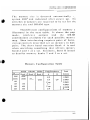
Next table
2-8
la;Nl';HAL I,'EATUHI';S
shows the automatic interleaving options that
OCClIr versus the nUlllber ur populated banks. In
the table, Bank 0,1,2 and J arc the designations
r 0 rca c h 0 r the r ou r [) R i\ 1\1 han k s. In the co I u III n s
below these designators, "Yes" or "Nu", indicate
whether the bank is populated.
Aut 0
III a
tic In' e r I e a l' e vs 1\1 e 111 0 r y 1\1 a p
Bank
0
Bank 1
Yes No
A Bank Address Mode
Linear
2
3
No
No
B Bank Address Mode N/A
Yes Yes 2-Way Interleave
No
No
N/A
Yes Yes 2- Way Interleave
Yes
No
Linear
Yes Yes 2- Way Interleave 0 and l '
Yes Yes 2-Way Interleave 2 and 3'
This is for the case where Banks A and I3 contain different
types of DRAMS. If all four banks contain the same DRAM
type then four-way interleaving is automatically activated.
Pagl' Mode Operatioll
Memory Interleaving operates independently
of page mode. Page mode is active whether one
bank or both arc populated.
The page mode
operation results in no additional wait state
penalty
for
either
reads
or
writes
which
immediately follow reads to the same DRAM page.
When
interleaving
are
installed
pairs
of
banks
enabled.
The
IS
automatically
2-9
GENERAL FEATURES
combination or page mode with interleaving
results in the best possible combination or fast
system memory operation using the most cost
effective DRAMs.
Shadow RAM
To further enhance the system performance,
shadow RAM is supported.
Shadow RAM is a
technique that loads system BIOS ,video and/or
adapter BIOS from the low speed EPROM/ROM
directly into fast DRAM during boot-up of the
computer. The execution of the BIOS then will
have significant improvement because. access to
DRAM is much faster than ROM.
Memory Remapping
If shadow RAM is not used at memory area
ODOOOOH:OEFFFFH, remapping is possible. Then,
local
memory
areas
OAOOOOH:OBFFFFH
and
ODOOOOH:OEFFFFH (each J 28K bytes) arc mapped
to the top of total memory for it to be used as
extended memory.
Memory areas OFOOOOH
OFFFFFH (system BIOS) and OCOOOOH-OCFFFFH
(video BIOS) are reserved for shadow RAM.
2-10
I/O SlJBSYSTEl\1
It IS vcry important that a high speed
system
should
be
compatible
with
existing
peripherals without downgrading the perrormance.
The Panther-II system is exactly designed with
this capability in mind.
To be compatible with
the existing add-on cards, user has the option of
defining the I/O speed.
If for example, the
peripheral card is not capable of operating at high
speed, user can define a slow speed for I/O slot
operation while still maintain the rest of the
system at very high speed.
2-11
GENERAL FEATURES
SYSTEM FUNCTIONS
System functions include
Interrupt
DMA
Timer
Real time clock
Clock and ready generation
I/O channel control
All system functions are [00% compatible to
AT standard.
I/O channel of Panther-II is
designed to be compatible with standard AT bus.
All the expansion cards conformed to the standard
AT bus can be used in Panther-II without problelll.
2-12
Chapter 3
Installing Conlponents
Warning: Be sure lo IItl'/l 0[[ Ihc cOmpIlICl"S
power swilCh he [ore i/lstallillg or I'C placing {IllY
componcnt.
I[ illstal/a/io/l sOlillds ri.,"-.!', /1'/ .1'0111' dCIII"I'
inslall the 80387SX.
I[ YOIl make a nlisLake. rOil
cOllld damage Ihe 8U387SX or .)'0111' cOli/pilleI'.
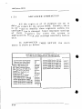
~lATH
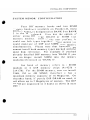
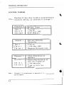
INSTALLING 80387SX
COPROCESSOR
Math coprocessor 80387SX is available in a
68-pin PLCC package. Find the 80387SX socket on
the s y s t e 111 boa rd. it's I() cat e d () 11 U I (1 a t the cor n e r
of the motherboard. The socket is a 6S-pin PLCC
socket, align the chip so that its orientation mark
matches up with that of the socket. When you arc
sure the pins arc aligned correctly. press firmly
and evenly on the 80387SX into the socket. Make
sure that the coprocessor is firmly inserted into
the socket.
The speed rating of 80387SX should match
that of the system speed for a optimum and
reliable operation.
Refer to the table below to
determine the correct speed rating of the 80387SX.
I
Panther-II
33 Mhz System
25 Mhz System
20 Mhz System
16 Mhz System
I
Ma t h Coprocessor
80387SX-33
80387SX-25
80387SX-20
80387SX-16
I
3-1
INSTALLING COMPONENTS
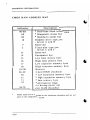
Orientation Marv
o
80387SX Coprocessor
Orientation Mark
1'-1 u mer icC 0
3-2
p r- 0 C e S S 0 r Soc vet
INSTALLING COMPONENTS
SYSTEM I\1EMOHY CONFIGURATION
Four DIP memory banks and two SIMM
memory banks are available on Panther-II, these
memory banks arc designated as BANK 0 to BANK
3 in the Illotherboard.
User has the option or
either uSing DIP type DRAM or SIMM type
memory modules.
Still if the user prefers, he
could usc both types together.
That means you
could make usc of DIP and SIMM type memory
simultaneously.
Please note that however, you
cannot install both memory types marked with the
same bank reference.
For example if you had
already installed DIP memory into 'BANK 0', you
can no longer install SIMM into the memory
modules referenced as 'BANK 0'.
One bank of memory rerers to 2 SIMM
modules or 6 DIP memory chips (4x44256 +
2x41256). For the SIMM memory, user can install
256K, 1M or 4M SIMM; therefore it has a
maximum memory capacity of 16 Megabytes. On
the other hand; if purely DIP DRAM are used, it
will allow up to 2 Megabytes of memory. The DIP
DRAM are organized in 4 banks as shown in next
page:
3-3
.f
INSTALLING COMPONENTS
DIP DRAM Memory Organization
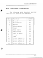
IMemory BanklDIP Memory LocationlDRAM Size
BANK 0
BANK I
BANK 2
BANK 3
U39,
U38,
U33,
U32,
U26,
U31,
U20,
U25,
U40, U41, U42
U37 (parity)
U34, U35, U36
U30 (parity)
U27, U28, U29
U24 (parity)
U21, U22, U23
UI9 (parity)
I
44256
41256
44256
41256
44256
41256
44256
41256
U38,U37, U32,U30, U31,U24 & U25,U19 are the parity
bits for
BANK 0 to BANK
3
respectively. In normal situation, those bits are not needed and the parity checking logic can bc disabled. Hence, the user can left those sockets unpopulated and thus allowing you to minimize the system cost. There are several combinations of DRAM
types you may consider. So, a basic system can be
equipped with fewer memory and later more
memory can be added when upgrading the system.
As a typical case, a basic system can be equipped
with 2 Megabyte memory using 1MB SIMM and
t. hen m e m 0 r y S i z c i s Iate r e x pan d e d t 0
I0 Megabytes by putting another banks or 4M SIMM. 3-4
iiI
WI
INSTALLlN(; COMPONENTS
The memory size IS detected automatically by
system BIOS and indicated after power up.
No
switches or jumpers are required to be set for the
memory size and DRAM type.
The different configurations of memory is
illustrated in the next table.
It shows the page
mude,
interleave
options
and
the
DRAM
combinations available for each possible memory
map. Since interleaving requires pairs of banks,
various controls described act on memory in bank
pairs.
The short hand nutatiun Bank A is used
when describing something that affects memory
banks 0 and I as a set. Similarly, Bank 13 is llsed
to describe memory banks 2 and 3 as a set.
Mcmory Configuration Tal>lc
16-Bit
Bank 0
Bank 1
256K
256K
256K
256K
1M
DRAM
Bank 2
25GK
Banks
Bank 3
256K
Page/Interleave
Total
B
Memory
2/P
10MB
4!P
4/P
2.0MB
A
Page
2.0MB
4.0MB
1M
1M
1M
4M
2/P
Page
10.0MB
4M
4M
2/P
16.0MB
3-5
INSTALLING COMPONENTS
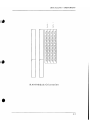
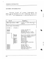
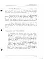
Installing SIMM Modules
Whenever adding memory modules to the
motherboard, install 2 modules at a time.
Also
make sure that the SIMM is installed in the
correct orientation, the RAM chips on the modules
should be facing the I/O slot. See the figure on
next page for illustration.
To install a module, the module edge should
angled into the socket's contact and then the
module is pivoted into position, where the locking
latches will secure it. If the module edge is not
completely inserted into the socket, it cannot be
pivoted to be in vertical position and should be
dragged out and inserted again. Do not force the
module into the SIMM sockct. It will damage the
locking latches.
The modules should be locked by the
locking latches of the sockets firmly.
Please
check carefully before turning on the power.
Otherwise, the system will not work properly.
3-6
INSTALLING COMPONENTS
~
z
-<
..c
7.
~
RAM Module Orientation
3-7
.
INSTALLING COMPONENTS
CONTROL OF SYSTEM SPEED
~)
System speed can be selected by hardware
switch and keyboard.
Connector P3 should be
connected to the turbo switch of the case panel,
this toggles the operation mode between turbo and
normal mode when pressed.
In addition to the front-panel switch, you
can also change the system speed via keyboard.
Press 'Ctrl', 'AIt' and '+' for turbo mode and
'Ctrl', 'Alt' and '-' for normal mode.
In either case, the turbo LED will light up
to indicate whether the system is now r,unning in
turbo mode or normal mode. In turbo mode, the
turbo LED will turned on. In normal mode, the
turbo LED is ofr.
It should be note that turbo switch setting
will override the keyboard switching mode, but
not vice versa.
3-8
~.
INSTALLING COMPONENTS
SYSTEM BOARD JUMPER SETTING
There arc a few jumpers in the motherboard
that allow the user to select the desired system
configuration.
The following tables show the
function and default settings or these jumpers.
Display Selectioll
I JP6 I
1-2
2-3
Display Type
Monochrome Display *
eGA, EGA, VGA, PGA
Defuul t settillf(
3-9
INSTALLING COMPONENTS
'CMOS Setup' Reset Jumper
Sometimes, improper setup may cause the
system to malfunction and you might not be ablc
to correct such problem without clearing the
entire CMOS Setup. The purpose of this jumper is
for the user to reset the CMOS Setup in case of
critical error occurred in the Setup. Make sure
that the power is OFF before you do this
operation. Also be certain that this jumper is rc
installed to its normal position after resetting the
CMOS Setup.
After the CMOS Setup is cleared, the Setup
will be loaded with the BIOS default value UpOIl
power-up and you may continue to define the
system configuration as usual.
I JP2 I
1-2
2-3
•
Default setting
3-10
Function
Normal opertaion *
Reset CMOS Setup
INSTALLING COMPONENTS
SYSTEM BOARD
CONNECTOI~S
Under typical conditions, these connectors
should be connected to the indicators and switches
of the system unit.
I
Connector
I
Function
PI
P2
P3
P4
Hardware reset con nector
Speaker connector
Turbo switch connector
Turbo LED connector
Power LED & Ext-Lock connector
Power supply connector
External battery connector
Keyboard connector
1'5
P6-P7
P8
KBI
Pin assignments
illustrated as follows:
or
the
connectors
are
P 1 - HardlVart: Rcst:l CVllllcclOr
I
Pin
I
2
I
Assignment
Selection Pin
Ground
3-11
INSTALLING COMPONENTS
P 2 - Speaker COllllec/or
I
Pin
I Assignment
I
Data out
+5 Vdc
Ground
+5 Vdc
2
3
4
P 3 - Turbo Switch Connector
I
Pin
I
2
I
Assignment
Selection Pin
Ground
P 4 - Turbo LED Connector
I
Pin
I
2
3-12
I Assign men t
+5 Vdc
LED signal
INSTALLING COMPONENTS
P
5 - POlVer LED & Ext-Lock CO/l/lcctor
I
Pin
I
1
2
3
4
5
P6-P7 - POlVer
I
Pin
Su fJp/.!' COl/l/coor
I
I
2
3
4
5
6
;\ssignl1lcIlI
POWERGOOD
+5 Vdc
+12 V de
- 1 2 Vdc
Ground
Ground
I
Pin
+5 Vde
Key
Ground
Keyboard in h i bit
Ground
2
3
4
5
6
I
Assignment
I
Assignmcnt
Ground
Ground
-5 Vdc
+5 V de
+5 Vdc
+5 Vde
3-13
INSTALLING COMPONENTS
P 8 - Exterllal Battery COllllector
I
Pin
I
2
3
4
I
Assignment
+ Vdc
not used
Grou nd
Ground
K B I - Keyboard COllnector
I
Pin
1
2
3
4
5
3-14
I Assignment
Keyboard clock
Keyboard da ta
Spare
Ground
+5 Vdc
Chapter 4
'ree hni ea I Info rlna t i() n
This section provides technical information
about Panther-II and is intended for advanced
users interested in the basic design and operation
or Panther-II.
MEI\IOHY I\IAPPING
I Address
II
Range
II
I
Function
0000007FFFFF
000K-512K
System Board Memory
(512K)
08000009FFFF
512K-640K
System Board
(128K)
01\0000OUFFFF
640K-768K
Display Bufrer (128K)
OCOOOOODFFFF
768K-896K
Adaptor ROM I
Shadow RAM (I28K)
OEOOOOOEFFFF
896K-960K
Systcm ROM / Shadow RAM (64K) OFOOOOOFFFFF
960K-1024K
System BIOS ROM / S had 0 w R A 1\1 (64 K ) 1000007FFFFF
1024K-8192K
System Mcmor)
800000FFFFI:F 8192 K - 1(13 18 K
Systcm IVIt; 111 () r y Memor~
4-1
TECHNICAL INFORMATION
I/O ADDRESS MAP
I/O Address Map all System Board
I/O address hex 000 to OFF are reserved for
the system board I/O.
ADDRESS
(HEX)
000-01 F
DMA Controller I, 8237
020-03F
Interrupt Controller I, 8259, Master
040-05F
Timer, 8254
060-06F
Keyboard Controller
070-07F
Real Time Clock, NMI
(non-maskable interrupt) mask
080-09F DMA Page Register, 74LS612
OAO-OBF Interrupt Controller 2, 8259
OCO-ODF DMA Controller 2, 8237
OFO Clear Math Coprocessor Busy
OF] Reset Math Coprocessor
OF8-0FF 4-2
I
DEVICE Math Coprocessor Port
TECHNICAL INFORMATION
I/O address hex 100 to 3FF arc available on
the I/O channel.
ADDRESS
(HEX)
DEVICE
I
IFO-IFS
Fixed Disk 200-207
Game I/O 27S-27F
Parallel Printer Port 2 2FS-2FF
Serial Port 2 300-31 F
Prototype Card 360-36F
Reserved 37S-37F
Parallel Printer Port I 3S0-3SF
S I) L C b i s y n~' h r () n () u s
~ 3AO-3AF
Bisynchronous I
3130-313F
Monochroille Display and Printer
Adapter
3CO-3CF
Reserved
3DO-3DF
Color Graphics ivlonitor Adapter
3FO-3F7
Diskette Controller
3FS-3FF
Serial Port I
4-3
TECHNICAL INFORMATION
SYSTEM TIMERS
Panther-II has three build-in programmable
timer/counters defined as channels 0 through 2 :
I
I
Channel 0
Tied on I. I 90 Mhz OSC 8259 IRQ 0 Channel I
Refresh Req uest
Genera tor
II Ga te I
Clk in I
Clk out I
Tied on
1.190 Mhz OSC
Request Refresh Cycle
Channel 2 Tone Genera tion of Speaker
I
Gate 2
Clk in 2 Clk ou t 2 4-4
System Timer
Gate 0
Clk in 0
Clk out 0
I
Ndte:
I
I
I
I
Controlled by bit 0 of
port hex 61 PPI bit
1.190 Mhz OSC
Used to drive the speaker Channel 1 is programmed to generate a i5-micro-second
period signal.
TECHNICAL INFORMATION
The 8254 ·I·imer/Collilters are treated by
system programs as an arrangement
rOllr
programmable external I/O ports.
Three are
treated as counters and the fourth is a control
register for mode programming.
or
,
4-5
TECHNICAL INFORMATION
SYSTEM INTERRUPTS
Sixteen levels of system interrupts are
provided on Panther-II. The following shows the
interrupt-level assignments in decreasing priority.
Level Function
Microprocessor N MI Parity or I/O Channel
Check
Interrupt Controllers
CTLR 1
CTLR 2
IRQO
IRQI
Timer Output 0
Keyboard
(Output Buffer Full)
Interrupt from CTLR 2
IRQ2 r
IRQ8
IRQ9
' - IRQIO
IRQII
IRQI2
IRQI3
IRQ14
IRQI5
Real-time Clock Interrupt
Software Redirected to
lNT OAH (lRQ2)
Reserved
Reserved
Reserved
Coprocessor
Fixed Disk Controller
Reserved
'-
IRQ3
IRQ4
IRQ5
IRQ6
IRQ7
4-6
Serial Port 2
Serial Port I
Parallel Port 2
Diskette Controller
Parallel Port I
TI~CHNICAL
INFORMATlON
DInECT I\IEI\IOHY ACCESS (DI\IA)
Panther-II supports seven Dl'v1A channels.
I
Channel
I
Function
0
Spa re (8 bit transfer) I
SDLC (8 hit t r:1 n s e r) 2
I-Ioppy Disk (8 bit transrer) :I
Spa re ( 8 hi t transfer) 4
Cascade
5
Spa re ( 16 bit transfer) 6
Spa re ( 16 bit transfer) 7
Spa re ( 16 bi I transfer) r
1'01'
DMA Controller I 4-7
TECHNICAL INFORMATION
The following shows the addresses for the
page register.
I
4-8
Page Register
I
I/O Address (HEX)
DMA Chan nel 0
0087
DMA Channel I
0083
DMA Channel 2
0081
DMA Channel 3
0082
DMA Channel 5
008B
DMA Channel 6
0089
DMA Channel 7
008A
Refresh
008F
TECHNICAL INFORMATION
REAL TIME CLOCK AND CI\105 HAM
., Real timc clock is build-in for maintaining
the limc and dalc. This SUbsyslcm also contains
114
bytes
of
RAM
III
addition
to
the
Clock/Calendcr. Thc Clock/Calendar information
and RAM arc kept active by connecting the device
to an external battery when systcm power is
turned ofr. Upon you turn the system power on,
CMOS will load thc recorded configuration into
the system so that the system can function in the
right track with thc cquippcd devices. Howcvcr,
if you have Hot l'ollfigurcd the (·i\10S. or the
bat t e r y w h i c h SLIP P () rt s the po \\. crt 0 the C M 0 Sis
weaken. you
nced to (clierine the necessary
parameters whcne\er the system is boot up.
rhe
rollowing page shows the CMOS RAi\1 addresses.
4-9
TECHNICAL INFORMATION
CMOS RAM ADDRESS MAP
I Addresses I
00-00
OE
OF
10
II
12
I3
14
15
16
17
18
19-20
2E-2F
30
31
32
33
34-7F
*
4-10
Description
* Real-time clock information
* Diagnostic sta tus byte
* Shutdown status byte
Diskette drive type byte
- drives A and B
Reserved
Fixed disk type byte
- drives C and 0
Reserved
Equipment byte
Low base memory byte
High base memory byte
Low expansion memory byte
High expansion memory byte
Reserved
2-byte CMOS checksum
* Low expansion memory byte
* High expansion memory byte
* Date century byte
* Information flags
(set during power on) User RAM (Standby) These bytes are not included in the checksum calculation and are not
part of the configuration record.
TECHNICAL INFORMATION
REAL TIME CLOCK INFORMATION
The following table describes real-time
clock bytes and specifics their addresses.
I
Byte
0
I
Address
Function
Seconds
00
I
Second alarm
01
2
Minutes
O~
3
Minute alarm
03
4
lIours
04
5
Hour ala rm
05
6
Da y
06
7
or week
Da t e or month
8
Mon th
08
9
Yea r
Oy
10
Status Register A
ot\
I I
Status Register
B
OB
12
Status Register C
OC
13
Status Register D
OD
07
4-11
TECHNICAL INFORMATION
SYSTEM EXPANSION BUS
Panther-II provides six expansion slots, four
of which are 16-bit and two are 8-bit expansion
slot.
The I/O channel supports:
*
I/O address space from hex 100 to hex 3FF
*
Selection of data access (either 8 or 16 bit)
*
24 bit memory addresses (16MB)
*
Interrupts
*
DMA channels
*
Memory refresh signal
4-12
TECIINICALINFORMATION
The
following
figure
shows
the
pin
numbering for I/O channcl connectors JI\I to J1\6.
REAR PANEL 81
A1 810
Al0
820
A20
831
A31
COMPONENT SIDE
4-13
TECHNICAL INFORMATION
The
following
figure
shows
the
pin
numbering for I/O channel connectors JBl-JB4.
REAR PANEL 01
C1 010
C10
018
C18
COMPONENT SIDE
I·
I
"
4-14
n":CIINICALINFORMATION
,
The
following
tables
summarize
assignments for the I/O channel connectors.
pin
I/O Challllel (A-Sid/')
I
I/O Pin
AI
A2
A3
A4
AS
A6
A7
A8
A9
A 10
All
A 12
A 13
A 14
A 15
A 16
A 17
A 18
A 19
A20
A21
A'"'')
A23
A24
A25
A 2()
A27
A28
A29
A30
A31
'--~
I
Signal Name
-I/O CH CK
S07
S06
SOS
S04
S03
S02
SOl
SOO
-I/O CH ROY
AEN
SA 19
SA 18
SA 17
SA 16
SA 15
SA 14
SA 13
SA 12
SA II
SAID
SA9
SA8
SA7
SA6
SA5
SA4
S;\3
S;\2
SAl
SAO
I
I/O
I
I/O
I/O
I/O
I/O
I/O
I/O
I/O
I/O
I
0
I/O
I/O
I/O
I/O
I/O
I/O
I/O
I/O
I/O
I/O
I/O
I/O
I/O
I/O
I
I/O
I/O
I/O
I/O
I/O
I/O
4-15
TECHNICAL INFORMATION
I/O Channel (B-Side)
~'
I
I
4-16
I/O Pin
BI
B2"
B3
B4
B5
B6
B7
B8
B9
BI0
B11
B12
B 13
BI4
B 15
B16
BI7
B 18
BI9
B20
B21
B22
B23
B24
B25
B26
B27
B28
B29
B30
B31
I
Signal Name
GND
RESET DRV
+5 Vdc
IRQ9
-5 Vdc
DRQ2
-12 V dc
OWS
+ 12 V dc
GND
-SMEMW
-SMEMR
-lOW
-lOR
-DACK3 DRQ3
-DACK 1
DRQI
-Refresh
ClK
IRQ7
IRQ6
IRQ5
IRQ4
IRQ3
-DACK2
T/C
BALE
+5 Vdc
OSC
GND
I
I/O
Ground
I
Power
I
Power
I
Power
I
Power
Grou od
0
0
I/O
I/O
.I
0
I
0
I/O 0
I
I
I
I
I
0
0
0
Power
0
Ground
I
TI';CIINICAL INFORMATION
,
J
I
1/0 Pin
CI
C2
C3
C4
C5
C6
C7
C8
C9
cIa
CII
C 12
CI3
CI4
C 15
CI6
CI7
C 18
I
Signal Name
SBHE
LA23
LA22
LA21
LA20
LA 19
LA 18
LA 17
-MEMR
-MEMW
S08
S09
SO 10
SOil
SOl2
SO 13
SO 14
SOl5
I
I/O
I/O
I/O
I/O
I/O
I/O
I/O
I/O
I/O
I/O
I/O
I/O
I/O
I/O
I/O
I/O
I/O
I/O
I/O
I
4-17
TECHNICAL INFORMATION
I/O Channel (D-Side)
I
4-18
I/O Pin
DI
D2
D3
D4
D5
D6
D7
D8
D9
D I0
D 11
DI2
DI3
Dl4
D 15
D 16
D 17
D 18
I
Signal Name
-MEM CSI6
-I/O CSI6
IRQIO
IRQ 11
IRQI2
IRQ 15
IRQI4
-DACKO
DRQO
-DACK5
DRQ5
-DACK6
DRQ6
-DACK 7
DRQ7
+5 Vdc
-MASTER
GND
I
I/O
I
I
I
I
I
1
I
0
I
0
I
0
I
0
I .
Power I
Ground I
Appendix A
AMI SYStCI11 BIOS
The system BIOS of Panther-II provides an
interface for operating systems and applications to
access the hardware. It is fully compatible with
standard AT BIOS and works flawlessly in the
network system.
It also performs self-test after
reset and includes a setup program to eonrigure
the s ys te m.
SELF-TEST
To ensure that the computer hardware is
fUllctional, thc systcm BIOS will carry Ollt a self
test upon rcsct.
The test is vcry intcnsivc and
covers all parts of hardware.
It takes a while
before messages are shown on the screen. It docs
not mean that the system is not working when the
screen is blank. So wait for a while after turning
on the power and listen carefully to thc speaker.
Some errors arc reported by a number or becp
sounds. Arter completing the self-test. the BIOS
will display some messages on the screen.
..~ In
case of serious errors, the BIOS will
suspend the test. If the display is not initialized.
the BIOS will report the error through a sequence
of becp sounds. Otherwise, crror message will bc
shown on the screcll.
A-I
AMI System BIOS
These fatal errors are usually communicated
through a series of audible beeps. The numbers
on the fatal error list below correspond to the
number of beeps for the corresponding error. All
errors listed, with the exception of #8, are fatal
errors.
No. of Beeps
I
2
3
4
5
6
7
8
9
10
Error Message
DRAM Refresh Failure
Base 64KB Memory Parity
Error
B'ase 64KB Memory Failure
System Time Failure
Processor Error
Keyboard Controller Gate
A20 Failure
Processor Exception
Interrupt Error
Display Memory Read /
Write Error (Video
Adapter)
ROM Checksum Error
CMOS Shutdown Register
Read/Write Error
If no error is found during self-test, the
system BIOS will proceed to boot from noppy disk
or hard disk.
The system BIOS will list the
system configuration on the screen shown in ncxt
page.
A-2
AMI System BIOS
System COllfiguratioll (C) Copyright 1985-1990, Americ:lll Megatrends Inc,
Main
l)rocCHS()f
Numeric Processor
Floppy Drive A:
Floppy Drive 1\
Display Type
ROM-BIOS Date
I(ll
bO:II«;
Ba~H~
None
1.2 Mil, 5'/,"
I -14 Mil, :\',,"
V(;A <or 1';l;A
Ext Memory Size
liard Disk C Type
"ard D 15k II TYPl'
25li \\1\
2
~l'ri,d
N\I!U'
1I5/ I()/~)I
I'arallel \'''1'1 (s)
MC!lI(lry Slze
I'"rl.(,)
(;.1()
N~'1H'
:11 \('
Do check the list to make sure that the
configuration IS correct.
Sometimes. problems
arise because or the incorrect information of the
configuration.
F () rex a III pie. if \' (HI r0 r get to
modify thc setup after changing the floppy disk
drive from one type to another. it can not boot
fro III rIo p p y dis k 0 r In a y not \\' 0 r k pro per I y . I r
you check the list. you can rind the cause or the
pro b I e 111.
A-3
AMI System BIOS
SYSTEM SETUP
The BIOS incorporates five setup sections:
(I)
(2)
(3)
(4)
(5)
Standard CMOS Setup
Advanced CMOS Setup
Advanced Chipset Setup
Auto Configuration with BIOS Defaults
Hard Disk Utilities
It is important that all the setup procedures
should be completed before operating the system.
Otherwise, the system may not run properly with
the incorrect setup information. Run the setup
again if the configuration is changed.
To enter the setup section, press 'DEL' when
the following message is shown after the power-on
memory test:
Hit <DEL> if you want to run SETUP
Whenever the system BIOS finds that the
configuration of the system is altered, a message
will be shown and you may press 'FI' to run setup.
Then the following messages are shown on the
screen.
A-4
AMI System BIOS
BIOS SETUP PROGHAM - AMI IlIOS SETUP UTILITIES
<C> 1990 American Megatrends, In:. All Rights Heserved
STANDARD CMOS SETUP ADVANCED CMOS SETUP ADVANCED CHIPSET SETUP AUTO CONFIGURATION WITH BIOS DEFAULTS lIARD DISK UTILITY WHITE TO CMOS AND EXIT DO NOT WRITE TO CMOS AND EXIT Standard CMOS setup for Changing Time, Date, liard Disk Type, etc. A-5
AMI System BIOS
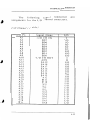
( 1 )
STANDARD CMOS SETUP
The memory size is automatically detected
by the BIOS. So you are only required to set the
d ate, tim e , h a r d dis k t y p e , no p p y d r i v est y pc,
display
type
and
keyboard.
The
system
configuration information arc shown as follows:
BIOS SETUP PROGRAM - STANDARD CMOS SETUP
(C) 1990 American Megat.rends Inc.; AU Right. Reserved
Date (mn/date/year)
Time (hour/min/lee)
Daylight Saving
Hard Dilk C; type
Hard Disk 0: type
:
Floppy Drive A:
Floppy Drive B:
Primary Di'play
Keyboard
Month:
Date
Year
Jan, Feb, .
.... Dec
01,02,03, ....... 31
1901,1902, ....... 2099
ESC:Exit,I~I-:Select
A-6
Sun. Jul 01, 1990
12 : 05 : 30
Disabled
Not Inst.lled
Not Installed
1.2 MB, 5'"
1.44 MB, 3%.
VGAor EGA
Installed
F2/F3:Co!or,PgUp/PgDn:Modify
Base memory size 640 KB
Ext. memory .ite ·256 KB
Cytn Head WPcom LZone Sect Size
Sun Mon Tue Wed Thu
Fri
Sat
1
2
3
4
5
6
7
S
9
10
11
12
13
14
15
16
17
18
19
20
21
22
23
24
25
26
27
,8
29
30
31
1
2
3
4
5
G
7
8
9
10
11
AMI System BIOS
Of>FION I
r I \I F.·' N /)
/),'
rF
Use PglJp and PgDn keys to change the
The date and time cannot be entered
va I ue.
An calender IS
directly by numeric values.
displayed on the lower right L'orner of the Serccn
for your reference.
OPTION 2
J
FIXED DISJ...· DRIIE
There are 47 types or fixed disks supported
by the BIOS. Consult your fixed disk manual to
determine its correct type. The parameters such
as cylinder number, head number, sector number
and pre-compensation must match your fixed
disk's parameters.
Use PgUp and PgDn keys to change the
fixed disk type. If the type of your fixed disk is
not included in the hard disk list, define a new
type as type 47. Use left and right arrow keys to
move between the parameter fields and enter the
parameters. The parameters will be stored in the
CMOS RAM and your fixed disk can be used
afterwards.
Each hard disk can be assigned a
different type 47 hard disk.
So two hard disks
w h i c h a· r e not inc Iud e din the lis t can b e use d
together in your system.
A-7
AMI System BIOS
If the type of fixed disk is wrong, it takes
a while before the BIOS can identify the error.
After setting the fixed disk type, if the system
haIts after reboot, please wait for a while. It is
most likely that the setting of fixed disk type is
incorrect.
When you install a new hard disk, make sure
whether it is already formatted. If not, the BIOS
has to check for a while before reporting the ha rd
disk error. In fact, the error arises only because
the hard disk is not formatted. If the hard disk
is formatted, you can run DOS FDISK and DOS
FORMAT.
Some fixed disks are specially handled and
must be set to 'Not Installed'. Consult the fixed
disk manual for details.
OPTION 3
FLOPPY DISK DRIVE
Four
supported:
types
l.
2.
3.
4.
A-8
5-Y,
5-'/,
3-Y,
3-y,
inch
inch
inch
inch
of
floppy
disk
drives
standard drive (360K)
high-density drive (1.2M)
sta nda rd d rive (720K)
high-density drive (1.44M)
are
__
AMI Systelll BIOS
The system BIOS supports two floppy disk
drives and they are recognized as drive A and B.
Select the correct types.
Otherwise the drives
cannot work properly.
If one of them is not
installed, select 'Not Installed' for that drive.
OPTION 4
DISPL~
Y
Four types or display arc supported:
I.
...,
-.
3.
4.
eGA 80
eGA 40
column mode
l' () I u m 11 mode
VGA/PGA/EGA
Monochrome
If the type or display is incorrect, the BIOS
will prompt you and ask you to set up again. But
the BIOS is still able to display messages on the
display attached to the system.
Thus you can
enter the setup program.
OPTION 5
K I:TH(),./ R D
If a keyboard is attached to the system,
select 'Installed'. The BIOS will test the keyboard
during selr-test.
A-9
AMI System BIOS
( 2 )
A D V A N C E D C M 0 SSE T U I'
All the registers of the chipsets are set to
default values by the system BIOS. Usually, there
is no need to modify these registers unless the
configuration is changed. Since improper settings
of these registers may cause the system to
malfunction, check your settings carefully before
exit.
In ADVANCED CMOS
menu is shown as below:
SETUP,
the
main
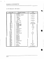
BIOS SETUP PROGRAM - ADVANCED CMOS SETUP
<c> 1990 American Megatrends Inc., All Rights Re!l:erved
Typematic Rate Programming
Disabled
Type",atic Rale Delay (M.ec)
Typernatic R:ate (Chftu/Sec)
: 500 : I~ : f)illlnbl(':d
Above 1 MB Memory Test
Memory Test Tick Sound
Hit <DEL> Me~sage Display
liard Di.k Type 47 RAM Are.
Wait (or <Fl> if Any Error
System Boot Up Num Lock
Numeric Proeessor
Floppy Drive Seek At Boot
System Boot Up Sequence
Video ROM Shadow COOO,I6K
Video ROM Shadow C400,16K
Adapter ROM Shadow C800,16K
Ad'pter ROM Shadow CCOO,I6K
Ad.pter ROM Shadow DOOO,I6K
Adapter ROM Sha.dow D400,16K
A-lO
:
:
:
Enabled
Enabled
0:300
Enabled
On
Disabled
Enabled
A:, C:
En:.bled
Enabled
Disabled
Di••bled
Disabled
:
Disabled
:
:
:
..
:
Adnplt!r ROM Shndow nROO,IGl<
Adapter ROM Shadow DCOO,I6K
Adapter nOM ShAdow EO()Q,ISI<
Adapter ROM Sh.dow E800,10K
Adapter ROM Shadow ECOn,1 GK
Adapter ROM Shadow EOOO.IGI(
Syotem ROM Shadow FOOO,16K
l)j~ahlf'(t
()i!tahlc(1
f)i~ahINI
l)i!'ahlf'ci
Di~flhled
Disabled
I)is;lbled
AMI Sy:;tt'1I111IOS
Artcr challgllig the regislels' sellings, lesl
your systcm rirst 1(1 l11al-..e sure that Ihc setlings
arc correct. It is likely thaI your s~stCI1l becomes
unstable and YOll need to setup the registers again.
In this section, you simply usc the up and
down arrow keys to move between options and
press PgUp/Pg\)n 10 scroll bit value.
Ariel' you
finish the Setup, press 'Esc' to return to main
menu. The BIOS will set the registers accordingly.
A short description rollows for each of the
options on the Advanced CMOS Setup Screen. 1['
any problem in somc options, press the <FI> Iklp
Key.
TYllcmatic I~atl' Programming:
By enabling this option, the user can adjust
thc rate at whil'h a keystroke is repeated. The
options
"Typel1latic
Rate
Delay"
and
"Typemalic Rate" also ancet this rate. When
a key is pressed and held down, the character
appears on the screen and, arter a delay set by
the
Typelllatie
Rate
Delay,
it
keeps on
repeating at a rate set by the Typematic Rate
Value.
When two or more keys arc pressed
and held down simultaneously, only the last
key pressed wiil be repeated at the typematie
rate. This stops when the last key pressed is
released, even if other keys are depressed.
A-ll
AMI System BIOS
Above 1 MB Memory Test:
If the option is enabled, the memory above 1MB will be tested. If disabled, it takes less time for memory test. Hard Disk Type 47 Data Area:
The AMI BIOS SETUP features two user definable hard disk types. Normally, the data
for these disk types are stored at 0:300 in
lower system RAM.
However, if a problem
occurs with some software regarding hard
disk, try setting this option to 'DOS I K U'.
IKB in the main memory will be allocated ror
hard disk type storage and the main'memory
is red uced to 639 KB. If shadow RAM for system BIOS (FOOOH) is
enabled, the hard disk type 47 will be added
to the standard hard disk type table. Henee
the hard disk type 47 data area is not needed
and this option is ignored. Hard disk type 47
will be considered as a standard hard disk
type by software. System Boot Up Num Lock:
The unum lock" option on the keyboard is
usually turned on after power on. This option
allows you to turn the "num lock" off after
power on. So you can use the arrow keys on
the numerie keypad without pressing the "num
lock" key. A-12
e
AMI System BIOS
N U IIIl' ri c I' r () C l' S S 0 r
These optiolls ~t1lo\\' the user to mark the
80387SX ~vlath coprocessor as present or absent.
Floppy Dri'l' Scck At Boot:
The default ror this option is "Enabled",
disabled, it allows a fast bool.
If
System Boot Up Sl'qucllce :
J
'1 his optioll allows you to choose which dri\ e
I h e s YSIC m \\ i II boo I r rom r irs t . The d era u I t
selting is ';\:, C:'. It allows you to boot from
device A if necessary.
lIo\\'e\er, it "ill
directly boot from hard disk when selecting
'C:, A:',
The 1310S will not read the floppy
disk A unless there is no drive C: installed,
Thus it takes less time for boot up.
V i d c () , A d a Jl t c r a /I II S ys t C III n 0 1\ Ish a II () "
The rca ret \\ 0 0 P t ion s tl r s had 0 \\' RAM r 0 r
video adapter, tell options or shadow RAM Jor
add-on card and one for the system 1310S. For
the option System ROM, the content of the
system at J()OOIl segment 1310S is copied to the
on board memory. For the option Video ROM,
the video ROM at COOOOII segment or C4000H
segment arc copied to memory.
A-13
AMI System BIOS
If you install an add-on card which ROM
BIOS locates at one of the Adapter ROM
shadow oPtions, you may select corresponding
option to shadow this ROM. Sometimes, there
may be problem after enabling the shadow
memory on the add-on card. In this case, you
cannot enable the shadow RAM function for
this add-on card.
A-14
AMI System BIOS
:,
ADVANCED CIIIPSET SETUll
( J )
DRAM Read Wait State
Options or '0 W/S' & 'I W/S' are
Check
carefully
whcther
your
suitable for the number or wait
want to select.
Improper setting
instability or the system.
available.
DRAM
is
states you
can cause
A setting o/" '0 WIS' will enable the system to
maximize its performance with zero wait state
memory
access
under
the
page/interleave
scheme.
On the other hand. a setling or 'I
W / S' w i I I a II 0 \\' I h e usc 0 I' I e sse:\. pen s i v e s low
DRAM bUI wilh perrormanl'e reduclion .
.f /1.\
(j
!;cl/cra/
1'/1/(':
For 33Mhz S\Slell1. you ma:- seleci '0 WIS' ir
I> R ;\ M w i I hac l' e s s I i III cor 7 OilS 0 I' r a SIC I' I S
used, otherwise seleci 'I W/S'.
For 25MHz and 20MHz system, you may select
'0 W / S' i I' D R A 1\1 \\' i t hac c e sst i 111 cor 80 n s a I'
r as t e r is usc d. u I her w is esc Icc t ' I \\' S'.
For \ 6 MHz s y sic 111. you I1LI \ sci e C I '0 W / S' i r
DRAM with access tillle or lOOns or raster is
used. otherwise select '\ W/S'.
Since the specification or DRAM varies among
difrerent manul'acturers; the above rule is not
a guarantee, you should consult your local
dealer ror the detail inrormation.
A-I5
AMI System DIOS
DHAM Write Wait State:
See 'DRAM Read Wait State' description above.
ATCLK Select
This controls the frequency at which the I/O
peripherals operate. The I/O performance can
be improved by selecting a higher AT bus
clock. However care should be exercised in
setting it, make sure that the peripheral cards
are capable of operating at higher speed
before making changes, otherwise problem
could arise.
Options of 'CLK2/8', 'CLK2/6' & 'CLK2/4' are
available, refer to the following table for the
corresponding I/O speed of different systems.
It is strongly recommended that the AT-Uus
speed be kept at or below 8.33 so as to comply
with ISA AT-Bus speeirication.
ATCLK Select(I/O Bus Speed)
System Speed
16MHz
CLK2/8
CLK2/6+
CLK2/4
4
5.33
8*
20MHz
5
6.67'
10
25MHz
6.25
8.33·
12.5
33M Hz
8*
11
16.5
+ Default Recommended values A-16
AMI Syst.cIIIIIIOS
2561\ B
Ct 1\1l'1II111")
Hl'llIc:I
lion:
The 256KB memory below 1MB boundary can
be used by software as extended memor) if
this option is enabled, therefore it is advisable
to enable this option. Otherwise, this area Lan
only be accesscd as shadow RAM function.
Ilowever,
256KU
memory
relocation
IS
automatically invalidated to avoid memory
contcntion if any memory segment between
ODOOOOH to OEFFFFII is enabled as shadow
RAM in the Advanced CMOS setup.
J
A-17
It
AMI System BIOS
(4 )
AUTO
CONFIGURATION
BIOS DEFAULTS
WITII
The Auto configuration with BIOS default
is used to set the internal registers of the system
to its optimum performance together with high
reliability.
Once the Auto Configuration IS
applied,
the
Advanced
CMOS
Setup
is
automatically re-configured with the default
settings; the user need not bother about the
settings in the ADVANCED CMOS SETUP.
But
you will still required to set those options in the
STANDARD
CMOS
SETUP
after
the
Auto
Configuration is used.
A-I8
Af\\1
Sy~tt'11l1l10S
II A I~ D DIS 1\ II TiLl T \
( 5 )
Hard Disk Utility program option is invoked
by selecting the 'HARD DISK UTILITY' at the
Main Setup Menu, the screen is shown as below:
BIOS SETUP PROGRAM
HARD DISK UTILITY
<c> 1990 American Meg!\tfends Inc .. All Rights Reserved
liard Di,k C:
Hard Disk D:
Type
Type:
47 USER TYPE
Cylin He",d WPeom LZone
1314
7
1314
1314
Sect
17
Si •• (MBI
76
Not Installed
Hard Disk Type c::m be changed from t.he STANDARD CMOS SETUP option in M:un Menu
--
H",rJ Disk Format Auto Interleave Medin AnalYSIS A-U)
AMI System BIOS
There are three options in the hard disk
utility: Hard Disk Format, Auto Interleave, and
Media Analysis.
For
a
new
hard
disk
(drive),
the
manufacturer of the hard drive usually provides
a list of "bad tracks" with the hard drive. Your
hard disk manual might also include the optimum
in terlea ve factor.
In this case, assuming that you have a list
of bad tracks and know the interleave factor, it
will not be necessary to take the auto interleave
and media analysis options.
Simply follow the
instructions in the Hard Disk Format.
If you
have a bad track list but have not been provided
with the optimum interleave factor, follow the
instructions in the Auto Interleave Section.
A-20
AMI Syslell.1I10S
U/'/"IUN I
-
;=.
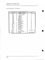
BIOS SETUP PIWGRAM
HARD DISK UTILITY
<C> 1990 American Megatrends Inc.,_ All Rights Reserved
Cylin Head WPc:.OIll Llone Sect
Ha.rd Disk C
Il:\rd Disk 0:
Type
H USER TVI'I:
Type
Not Installed
1314
7
1314
13 J.I
Auto Interleave
Site (MB)
17
Bad Track
Di,k Drive (C/O)
? C
Disk Drive Type
? H
M>rk Bad Track. (Y /N) 7 N
Procef"d (Y IN)
Ms.
Cyln.
7G
%
Head
7
,,=
-
Use the
liard
integrate a new hard
rerormat a used hard
some bad tracks. To
used drive, select the
I
Disk
Format option
to
disk to the system, or to
disk which has developed
find these bad tracks on a
Media Analysis option.
The value for Disk Drive is C for a C:
Drive or D for a D: Drive.
If two disk drives
have been previously entered at the Standard
CMOS Setup Scree, then the 10 (C/O) will appear
to the right of the question mark following the
Disk Drive field. Choose which drive you wish to
format by selecting the appropriate letter and
pressing <ENTER>. If only one drive was selected
at the Standard CMOS Setup Screen, the Cursor
A-21
.
AMI System BIOS
OPTION 3
/llEDIA ANALYSIS UTILITY
BIOS SETUP PROGRAM - HARD DISK UTILITY
<C> 1990 American Megatrend3 Inc.," All Rights Reserved
Hard Di.k C:
Hard Disk D:
Type:
Type:
~7
USER TYPE
Not Installed
Cylin Head WPcom LZone Sect
7
1314
1314
\7
1314
Site (MB)
76
Media Analysis
Disk Drive (C/O)
Disk Drive Type
Proceed (Y /N)
? C
47
?
1
The Media Analysis Utility performs a
series of tests to locate bad tracks on the hn rd
disk.
All bad tracks on the hard disk will be
listed in the Bad Track List Box. Since this test
writes to all cylinders and heads on thc hard disk
to verify andy bad tacks, the test may require
several minutes to complete.
A-24
Appendix B
Operation and Maintenance
(I
SOllie
of tbe
Panther-II
or
arc static-sensiti\e deviccs
by static discharges.
To
thc device ma) bc wrapped
anti-static
bag;
certain
taken before rcmoving the
COlllpOllellts
computer componcnts
and can be damagcd
prevent such damagc.
in
a
conducti\'e.
precautions should he
device from its bags.
W hen ins t a II i n g 0 r rem 0 \' i n g any add - 0 n
card. DRAM module or coprocessor, care should be
taken when handling these devices.
Touch an
unpaint metal part of vour system unit (for
example, the screws on the rear of the system
unit) with onc hand. thell hold the component you
arc installing on thc other hanel. This will place
your body, the component. and the system unit at
the
same
ground
potential.
preventing
an
accidental stati\.· discharge,
Be sure to handle
circuit boards b) the edges onl) and do not touch
the component pins or solder joints,
Grasp
diskette drives or fixed disk elri\es by their
frames to avoid touching the circuit board.
Memory chips or co-processor should be held by
their bodies only. not by their pins.
Preventing a problem is better than having
to fix it after it has happened.
This is where
cleanliness and proper operating procedures come
into play.
8-1
OPERATION AND MAINTENANCE
KEEPING TilE SYSTEM COOL
Airflow is critical for proper operation.
The
motherboard
contains
many
high-speed
components and they will generate heat during
operation.
Other add-on cards and hard disk
drive can also produce a lot of heat. As a result,
the temperature inside the computer system may
be very high.
These boards require cool air to
prevent a deadly heat build-up. Be sure that all
cooling vents in the front or sides of the computer
are open and that air circulation is good. Check
the clearance at the back of the computer; the
power supply contains a fan to blow air out of the
case, make sure the fan is not blocked by cables
or papers. Don't push your computer flush against
the wall; leave it some breathing space. Heat can
destroy compu ter ch ips.
CLEANING THE "GOLDEN FINGER"
Whenever inserting an add-on card to the
motherboard, make sure that there is no dirt on
the "golden finger" of the add-on card. If not, the
contact between the "golden finger" and the slot
may be poor and thus causing the add-on cards to
work improperly. Use a pencil eraser to clean the
"golden finger" if din is found.
B-2
OPI';HATION AND MAINTENANCE
CLEANINC TilE I\IOTtlEnnOAI{1)
Because the system is air-cooled, dust can
enter your system through the ventilation slots.
At least once a year, take the cover off your
computer and vacuum the interior to remove
accumulated dust. Use a brush attachment on the
vacuum and carcfully go ovcr all exposed parts.
To prevent dust frolll accumulating on the mother
board, installing all mounting plates on the rear
of the casco Regularly examine your system, and
if necessary, vacuum the interior of the system
with a miniature vacuum.
13-3
OPERATION AND MAINTENANCE
THIS PAGE IS INTENTIONALLY LEFT BLANK
8-4
Appendix C
Systelll Board Layoll t
(t
1
1
.'I,.OCTEK
D3P 1
ih LP'_-_-2=75='2===I,rl,--=--=--=--=--=--=--=--=--=--=-:-=--=--=--=--=--=-~~~~-=--=--=--=--=--=--=
1 PA.NTHER II 386SX
1
_
JPI
,
,
]
]
JP2
0'
01
o
II
6<l386SX
pe
0'
~~~~
I
00367SX
D
44256
44256
BANK 3
f41256
I
~
.42~6
IF
442!'l6
IF
I~
44256
I ~ «256 I ~
IF
IF
44256.J
BANK 2
~ ~.1~56
~
«2~e
4"2M
442~6
«256
44256
44256
4..1.;]58
BANK 1
I p.U256 I
(I
(: - I


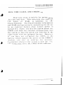

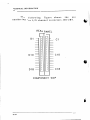

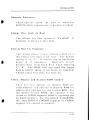


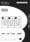


![PLAS A O ]-OR](http://vs1.manualzilla.com/store/data/005852706_1-5db0b7ed584537f0e62af161fb124638-150x150.png)