1
Preliminary User’s Manual
DCAN Macro
Version B2
Document No. U14668EE3V0UM00
Date Published May 2002
NEC Corporation 2002
Printed in Germany
NOTES FOR CMOS DEVICES
1
PRECAUTION AGAINST ESD FOR SEMICONDUCTORS
Note:
Strong electric field, when exposed to a MOS device, can cause destruction of the gate oxide and
ultimately degrade the device operation. Steps must be taken to stop generation of static electricity
as much as possible, and quickly dissipate it once, when it has occurred. Environmental control
must be adequate. When it is dry, humidifier should be used. It is recommended to avoid using
insulators that easily build static electricity. Semiconductor devices must be stored and transported
in an anti-static container, static shielding bag or conductive material. All test and measurement
tools including work bench and floor should be grounded. The operator should be grounded using
wrist strap. Semiconductor devices must not be touched with bare hands. Similar precautions need
to be taken for PW boards with semiconductor devices on it.
2
HANDLING OF UNUSED INPUT PINS FOR CMOS
Note:
No connection for CMOS device inputs can be cause of malfunction. If no connection is provided
to the input pins, it is possible that an internal input level may be generated due to noise, etc., hence
causing malfunction. CMOS devices behave differently than Bipolar or NMOS devices. Input levels
of CMOS devices must be fixed high or low by using a pull-up or pull-down circuitry. Each unused
pin should be connected to V DD or GND with a resistor, if it is considered to have a possibility of
being an output pin. All handling related to the unused pins must be judged device by device and
related specifications governing the devices.
3
STATUS BEFORE INITIALIZATION OF MOS DEVICES
Note:
Power-on does not necessarily define initial status of MOS device. Production process of MOS
does not define the initial operation status of the device. Immediately after the power source is
turned ON, the devices with reset function have not yet been initialized. Hence, power-on does
not guarantee out-pin levels, I/O settings or contents of registers. Device is not initialized until the
reset signal is received. Reset operation must be executed immediately after power-on for devices
having reset function.
2
Preliminary User’s Manual U14668EE3V0UM00
MS-DOS and MS-Windows are either registered trademarks or trademarks of Microsoft
Corporation in the United States and/or other countries.
PC/AT and PC DOS are trademarks of IBM Corp.
The related documents in this publication may include preliminary versions. However, preliminary
versions are not marked as such.
The export of this product from Japan is regulated by the Japanese government. To export this
product may be prohibited without governmental license, the need for which must be judged by th
customer. The export or re-export of this product from a country other than Japan may also be
prohibited without a license from that country. Please call an NEC sales representative.
The information in this document is current as of 02.05.2002. The information is subject to change without
notice. For actual design-in, refer to the latest publications of NEC’s data sheets or data books, etc., for
the most up-to-date specifications of NEC semiconductor products. Not all products and/or types are
available in every country. Please check with an NEC sales representative for availability and additional
information. No part of this document may be copied or reproduced in any form or by any means without
prior written consent of NEC. NEC assumes no responsibility for any errors that may appear in this
document. NEC does not assume any liability for infringement of patents, copyrights or other intellectual
property rights of third parties by or arising from the use of NEC semiconductor products listed in this
document or any other liability arising from the use of such products. No license, express, implied or
otherwise, is granted under any patents, copyrights or other intellectual property rights of NEC or others.
Descriptions of circuits, software and other related information in this document are provided for illustrative
purposes in semiconductor product operation and application examples. The incorporation of these
circuits, software and information in the design of customer’s equipment shall be done under the full
responsibility of customer. NEC assumes no responsibility for any losses incurred by customers or third
parties arising from the use of these circuits, software and information. While NEC endeavours to enhance
the quality, reliability and safety of NEC semiconductor products, customers agree and acknowledge that
the possibility of defects thereof cannot be eliminated entirely. To minimize risks of damage to property
or injury (including death) to persons arising from defects in NEC semiconductor products, customers must
incorporate sufficient safety measures in their design, such as redundancy, fire-containment and antifailure features. NEC semiconductor products are classified into the following three quality grades:
“Standard”, “Special” and “Specific”. The “Specific” quality grade applies only to semiconductor products
developed based on a customer-designated “quality assurance program” for a specific application. The
recommended applications of a semiconductor product depend on its quality grade, as indicated below.
Customers must check the quality grade of each semiconductor product before using it in a particular
application.
"Standard": Computers, office equipment, communications equipment, test and measurement equipment, audio and visual equipment, home electronic appliances, machine tools, personal
electronic equipment and industrial robots.
"Special": Transportation equipment (automobiles, trains, ships, etc.), traffic control systems, antidisaster systems, anti-crime systems, safety equipment and medical equipment (not specifically designed for life support).
"Specific": Aircrafts, aerospace equipment, submersible repeaters, nuclear reactor control systems, life
support systems or medical equipment for life support, etc.
The quality grade of NEC semiconductor products is “Standard“ unless otherwise expressly specified in
NEC's data sheets or data books, etc.
If customers wish to use NEC semiconductor products in applications not intended by NEC, they must
contact an NEC sales representative in advance to determine NEC's willingness to support a given
application.
Notes: (1) “NEC” as used in this statement means NEC Corporation and also includes its majority-owned
subsidiaries.
(2) “NEC semiconductor products” means any semiconductor product developed or manufactured
by or for NEC (as defined above).
M5 2000.03
Preliminary User’s Manual U14668EE3V0UM00
3
Regional Information
Some information contained in this document may vary from country to country. Before using any NEC
product in your application, please contact the NEC office in your country to obtain a list of authorized
representatives and distributors. They will verify:
•
Device availability
Ordering information
Product release schedule
Availability of related technical literature
Development environment specifications (for example, specifications for third-party tools and
components, host computers, power plugs, AC supply voltages, and so forth)
Network requirements
In addition, trademarks, registered trademarks, export restrictions, and other legal issues may also vary
from country to country.
NEC Electronics Inc. (U.S.)
Santa Clara, California
Tel: 408-588-6000
800-366-9782
Fax: 408-588-6130
800-729-9288
NEC Electronics (Europe) GmbH
Duesseldorf, Germany
Tel: 0211-65 03 01
Fax: 0211-65 03 327
Sucursal en España
Madrid, Spain
Tel: 091-504 27 87
Fax: 091-504 28 60
Succursale Française
Vélizy-Villacoublay, France
Tel: 01-30-67 58 00
Fax: 01-30-67 58 99
Filiale Italiana
Milano, Italy
Tel: 02-66 75 41
Fax: 02-66 75 42 99
NEC Electronics Hong Kong Ltd.
Hong Kong
Tel: 2886-9318
Fax: 2886-9022/9044
Branch The Netherlands
Eindhoven, The Netherlands
Tel: 040-244 58 45
Fax: 040-244 45 80
NEC Electronics Hong Kong Ltd.
Seoul Branch
Seoul, Korea
Tel: 02-528-0303
Fax: 02-528-4411
Branch Sweden
Taeby, Sweden
Tel: 08-63 80 820
Fax: 08-63 80 388
United Kingdom Branch
Milton Keynes, UK
Tel: 01908-691-133
Fax: 01908-670-290
NEC Electronics Singapore Pte. Ltd.
Singapore
Tel: 65-253-8311
Fax: 65-250-3583
NEC Electronics Taiwan Ltd.
Taipei, Taiwan
Tel: 02-2719-2377
Fax: 02-2719-5951
NEC do Brasil S.A.
Electron Devices Division
Guarulhos, Brasil
Tel: 55-11-6465-6810
Fax: 55-11-6465-6829
4
Preliminary User’s Manual U14668EE3V0UM00
Introduction
Readers
This manual has been prepared for engineers who want to understand the
functions of the DCAN Macro and design and develop its application systems
and programs.
Purpose
This manual is intended for users to understand the functions described in
the Organization below.
Organization
The DCAN Macro manual is separated into two parts: an explanation of the
CAN protocol and a detailed description of the DCAN macro.
How to read
this Manual
Before reading this manual, you should have general knowledge of electric
and logic circuits and microcontrollers:
•
When you want to have an introduction to the CAN protocol and want to
understand the function of the DCAN:
- Read this manual in the order of the contents.
•
When you have a good command on the CAN protocol and want only to
understand the DCAN function:
- Start reading from Chapter 4 onwards.
Legend
Symbols and notation are used as follows:
Weight in data notation : Left is high-order column, right is low order column
Active low notation
: xxx (pin or signal name is over-scored) or
/xxx (slash before signal name)
Memory map address: : High order at high stage and low order at low stage
Note
: Explanation of (Note) in the text
Caution
: Item deserving extra attention
Remark
: Supplementary explanation to the text
Numeric notation
: Binary . . . XXXX or XXXB
Decimal . . . XXXX
Hexadecimal . . . XXXXH or 0x XXXX
Prefixes representing powers of 2 (address space, memory capacity)
K (kilo): 210 = 1024
M (mega): 220 = 10242 = 1,048,576
G (giga): 230 = 10243 = 1,073,741,824
Preliminary User’s Manual U14668EE3V0UM00
5
Chapter Organization
This manual divides the descriptions for the DCAN into different chapters as
shown below.
Chapter
Chapter 1
Outline Description
Chapter 2
CAN Protocol
Chapter 3
Function
Chapter 4
Connection with Target System
Chapter 5
DCAN Controller Configuration
Chapter 6
Special Function Register for DCAN-module
Chapter 7
Message Buffer Configuration
Chapter 8
Transmit Buffer Structure
Chapter 9
Transmit Message Buffer Format
Chapter 10
Receive Buffer Structure
Chapter 11
Receive Message Buffer Format
Chapter 12
Mask Function
Chapter 13
Operation of the DCAN Controller
Chapter 14
Baud Rate Generation
Chapter 15
Function Control
Chapter 16
Interrupt Information
Chapter 17
Power Saving Modes
Chapter 18
Functional Description by Flowcharts
Related Documents
6
The content of this document (issue April 2002) addresses the DCAN macro
version B2. Differences to older versions are indicated but not described. For
particular information on memory or register addresses that are not mentioned in this document, the respective user manual of the product needs to
be checked.
Preliminary User’s Manual U14668EE3V0UM00
Table of Contents
Introduction. . . . . . . . . . . . . . . . . . . . . . . . . . . . . . . . . . . . . . . . . . . . . . . . . . . . 5
Chapter 1
Outline Description . . . . . . . . . . . . . . . . . . . . . . . . . . . . . . . . . . . . . . . . . . . . 13
Chapter 2
CAN Protocol . . . . . . . . . . . . . . . . . . . . . . . . . . . . . . . . . . . . . . . . . . . . . . . . . 15
2.1
2.2
2.3
Protocol Mode Function . . . . . . . . . . . . . . . . . . . . . . . . . . . . . . . . . . . . . . . . . . . . . . . . 15
Message Format. . . . . . . . . . . . . . . . . . . . . . . . . . . . . . . . . . . . . . . . . . . . . . . . . . . . . . . 16
Data Frame / Remote Frame . . . . . . . . . . . . . . . . . . . . . . . . . . . . . . . . . . . . . . . . . . . . . 17
2.3.1
Description of each field . . . . . . . . . . . . . . . . . . . . . . . . . . . . . . . . . . . . . . . . . . . 18
2.4
Error Frame . . . . . . . . . . . . . . . . . . . . . . . . . . . . . . . . . . . . . . . . . . . . . . . . . . . . . . . . . . 24
2.5
Overload Frame . . . . . . . . . . . . . . . . . . . . . . . . . . . . . . . . . . . . . . . . . . . . . . . . . . . . . . . 25
Chapter 3
3.1
3.2
3.3
3.4
3.5
3.6
3.7
3.8
Function . . . . . . . . . . . . . . . . . . . . . . . . . . . . . . . . . . . . . . . . . . . . . . . . . . . . . 27
Arbitration. . . . . . . . . . . . . . . . . . . . . . . . . . . . . . . . . . . . . . . . . . . . . . . . . . . . . . . . . . . . 27
Bit Stuffing . . . . . . . . . . . . . . . . . . . . . . . . . . . . . . . . . . . . . . . . . . . . . . . . . . . . . . . . . . . 28
Multi Master . . . . . . . . . . . . . . . . . . . . . . . . . . . . . . . . . . . . . . . . . . . . . . . . . . . . . . . . . . 28
Multi Cast . . . . . . . . . . . . . . . . . . . . . . . . . . . . . . . . . . . . . . . . . . . . . . . . . . . . . . . . . . . . 28
Sleep Mode/Stop Function . . . . . . . . . . . . . . . . . . . . . . . . . . . . . . . . . . . . . . . . . . . . . . 28
Error Control Function . . . . . . . . . . . . . . . . . . . . . . . . . . . . . . . . . . . . . . . . . . . . . . . . . 29
Baud Rate Control Function . . . . . . . . . . . . . . . . . . . . . . . . . . . . . . . . . . . . . . . . . . . . . 32
State Shift Chart . . . . . . . . . . . . . . . . . . . . . . . . . . . . . . . . . . . . . . . . . . . . . . . . . . . . . . . 35
Chapter 4
Connection with Target System . . . . . . . . . . . . . . . . . . . . . . . . . . . . . . . . . . 39
Chapter 5
DCAN Controller Configuration . . . . . . . . . . . . . . . . . . . . . . . . . . . . . . . . . . 40
Chapter 6
Special Function Register for DCAN-module . . . . . . . . . . . . . . . . . . . . . . . 41
Chapter 7
Message Buffer Configuration . . . . . . . . . . . . . . . . . . . . . . . . . . . . . . . . . . . 43
Chapter 8
Transmit Buffer Structure. . . . . . . . . . . . . . . . . . . . . . . . . . . . . . . . . . . . . . . 44
Chapter 9
9.1
9.2
9.3
Transmit Message Buffer Format . . . . . . . . . . . . . . . . . . . . . . . . . . . . . . . . . 45
Transmit Message Definition . . . . . . . . . . . . . . . . . . . . . . . . . . . . . . . . . . . . . . . . . . . . 46
Transmit Identifier Definition . . . . . . . . . . . . . . . . . . . . . . . . . . . . . . . . . . . . . . . . . . . . 47
Transmit Data Definition . . . . . . . . . . . . . . . . . . . . . . . . . . . . . . . . . . . . . . . . . . . . . . . . 48
Chapter 10 Receive Buffer Structure . . . . . . . . . . . . . . . . . . . . . . . . . . . . . . . . . . . . . . . . 49
Chapter 11 Receive Message Buffer Format . . . . . . . . . . . . . . . . . . . . . . . . . . . . . . . . . 50
11.1
11.2
11.3
11.4
Receive Control Bits Definition . . . . . . . . . . . . . . . . . . . . . . . . . . . . . . . . . . . . . . . . . . 51
Receive Status Bits Definition . . . . . . . . . . . . . . . . . . . . . . . . . . . . . . . . . . . . . . . . . . . 52
Receive Identifier Definition . . . . . . . . . . . . . . . . . . . . . . . . . . . . . . . . . . . . . . . . . . . . . 54
Receive Message Data Part . . . . . . . . . . . . . . . . . . . . . . . . . . . . . . . . . . . . . . . . . . . . . 55
Chapter 12 Mask Function . . . . . . . . . . . . . . . . . . . . . . . . . . . . . . . . . . . . . . . . . . . . . . . . 57
12.1
12.2
12.3
Identifier Compare with Mask . . . . . . . . . . . . . . . . . . . . . . . . . . . . . . . . . . . . . . . . . . . . 58
Mask Identifier Control Register (MCON) . . . . . . . . . . . . . . . . . . . . . . . . . . . . . . . . . . 59
Mask Identifier Definition . . . . . . . . . . . . . . . . . . . . . . . . . . . . . . . . . . . . . . . . . . . . . . . 60
Chapter 13 Operation of the DCAN Controller . . . . . . . . . . . . . . . . . . . . . . . . . . . . . . . . 61
13.1
13.2
13.3
DCAN Control Register (DCANCn) . . . . . . . . . . . . . . . . . . . . . . . . . . . . . . . . . . . . . . . . 61
CAN Control Register (CANCn) . . . . . . . . . . . . . . . . . . . . . . . . . . . . . . . . . . . . . . . . . . 62
DCAN Error Status Register . . . . . . . . . . . . . . . . . . . . . . . . . . . . . . . . . . . . . . . . . . . . . 67
Preliminary User’s Manual U14668EE3V0UM00
7
13.4
13.5
13.6
CAN Transmit Error Counter. . . . . . . . . . . . . . . . . . . . . . . . . . . . . . . . . . . . . . . . . . . . . 70
CAN Receive Error Counter . . . . . . . . . . . . . . . . . . . . . . . . . . . . . . . . . . . . . . . . . . . . . 70
Message Count Register . . . . . . . . . . . . . . . . . . . . . . . . . . . . . . . . . . . . . . . . . . . . . . . . 71
Chapter 14 Baud Rate Generation . . . . . . . . . . . . . . . . . . . . . . . . . . . . . . . . . . . . . . . . . . 73
14.1
14.2
Bit Rate Prescaler Register . . . . . . . . . . . . . . . . . . . . . . . . . . . . . . . . . . . . . . . . . . . . . . 73
Synchronization Control Registers 0 and 1. . . . . . . . . . . . . . . . . . . . . . . . . . . . . . . . . 75
Chapter 15 Function Control . . . . . . . . . . . . . . . . . . . . . . . . . . . . . . . . . . . . . . . . . . . . . . 79
15.1
Transmit Control . . . . . . . . . . . . . . . . . . . . . . . . . . . . . . . . . . . . . . . . . . . . . . . . . . . . . . 79
15.1.1
Transmit Control Register . . . . . . . . . . . . . . . . . . . . . . . . . . . . . . . . . . . . . . . . 79
15.2 Receive Control . . . . . . . . . . . . . . . . . . . . . . . . . . . . . . . . . . . . . . . . . . . . . . . . . . . . . . . 82
15.2.1
Receive Message Register. . . . . . . . . . . . . . . . . . . . . . . . . . . . . . . . . . . . . . . . 82
15.3 Mask Control . . . . . . . . . . . . . . . . . . . . . . . . . . . . . . . . . . . . . . . . . . . . . . . . . . . . . . . . . 83
15.3.1
Mask Control Register . . . . . . . . . . . . . . . . . . . . . . . . . . . . . . . . . . . . . . . . . . . 83
15.4 Special Functions . . . . . . . . . . . . . . . . . . . . . . . . . . . . . . . . . . . . . . . . . . . . . . . . . . . . . 86
15.4.1
Redefinition Control Register . . . . . . . . . . . . . . . . . . . . . . . . . . . . . . . . . . . . . 86
15.5 Performance of the DCAN . . . . . . . . . . . . . . . . . . . . . . . . . . . . . . . . . . . . . . . . . . . . . . . 88
Chapter 16 Interrupt Information . . . . . . . . . . . . . . . . . . . . . . . . . . . . . . . . . . . . . . . . . . . 89
16.1
16.2
16.3
16.4
Interrupt Vectors . . . . . . . . . . . . . . . . . . . . . . . . . . . . . . . . . . . . . . . . . . . . . . . . . . . . . . 89
Transmit Interrupt . . . . . . . . . . . . . . . . . . . . . . . . . . . . . . . . . . . . . . . . . . . . . . . . . . . . . 89
Receive Interrupt . . . . . . . . . . . . . . . . . . . . . . . . . . . . . . . . . . . . . . . . . . . . . . . . . . . . . . 89
Error Interrupt. . . . . . . . . . . . . . . . . . . . . . . . . . . . . . . . . . . . . . . . . . . . . . . . . . . . . . . . . 90
Chapter 17 Power Saving Modes . . . . . . . . . . . . . . . . . . . . . . . . . . . . . . . . . . . . . . . . . . . 91
17.1
17.2
17.3
17.4
17.5
CPU Halt Mode . . . . . . . . . . . . . . . . . . . . . . . . . . . . . . . . . . . . . . . . . . . . . . . . . . . . . . . . 91
CPU WATCH Mode. . . . . . . . . . . . . . . . . . . . . . . . . . . . . . . . . . . . . . . . . . . . . . . . . . . . . 91
CPU Stop Mode . . . . . . . . . . . . . . . . . . . . . . . . . . . . . . . . . . . . . . . . . . . . . . . . . . . . . . . 91
DCAN Sleep Mode . . . . . . . . . . . . . . . . . . . . . . . . . . . . . . . . . . . . . . . . . . . . . . . . . . . . . 91
DCAN Stop Mode . . . . . . . . . . . . . . . . . . . . . . . . . . . . . . . . . . . . . . . . . . . . . . . . . . . . . . 93
Chapter 18 Functional Description by Flowcharts . . . . . . . . . . . . . . . . . . . . . . . . . . . . . 95
18.1
18.2
18.3
18.4
18.5
18.6
8
Initialization . . . . . . . . . . . . . . . . . . . . . . . . . . . . . . . . . . . . . . . . . . . . . . . . . . . . . . . . . . 95
Transmit Preparation . . . . . . . . . . . . . . . . . . . . . . . . . . . . . . . . . . . . . . . . . . . . . . . . . . . 96
Abort Transmit . . . . . . . . . . . . . . . . . . . . . . . . . . . . . . . . . . . . . . . . . . . . . . . . . . . . . . . . 97
Handling by the DCAN. . . . . . . . . . . . . . . . . . . . . . . . . . . . . . . . . . . . . . . . . . . . . . . . . . 98
Receive Event Oriented . . . . . . . . . . . . . . . . . . . . . . . . . . . . . . . . . . . . . . . . . . . . . . . . . 99
Receive Task Oriented. . . . . . . . . . . . . . . . . . . . . . . . . . . . . . . . . . . . . . . . . . . . . . . . . 100
Preliminary User’s Manual U14668EE3V0UM00
List of Figures
Figure 1-1:
Figure 2-1:
Figure 2-2:
Figure 2-3:
Figure 2-4:
Figure 2-5:
Figure 2-6:
Figure 2-7:
Figure 2-8:
Figure 2-9:
Figure 2-10:
Figure 2-11:
Figure 2-12:
Figure 2-13:
Figure 2-14:
Figure 2-15:
Figure 3-1:
Figure 3-2:
Figure 3-3:
Figure 3-4:
Figure 3-5:
Figure 3-6:
Figure 4-1:
Figure 9-1:
Figure 9-2:
Figure 9-3:
Figure 11-1:
Figure 11-2:
Figure 11-3:
Figure 11-4:
Figure 12-1:
Figure 12-2:
Figure 12-3:
Figure 13-1:
Figure 13-2:
Figure 13-3:
Figure 13-4:
Figure 13-5:
Figure 13-6:
Figure 13-7:
Figure 13-8:
Figure 13-9:
Figure 13-10:
Figure 13-11:
Figure 14-1:
Figure 14-2:
Figure 15-1:
Figure 15-2:
Figure 15-3:
Figure 15-4:
Figure 18-1:
Figure 18-2:
Figure 18-3:
Figure 18-4:
Figure 18-5:
Structural Block Diagram............................................................................................. 13
Data Frame ................................................................................................................. 17
Remote Frame ............................................................................................................ 17
Data Frame ................................................................................................................. 18
Arbitration Field/Standard Format Mode ..................................................................... 18
Arbitration Field/Extended Format Mode..................................................................... 19
Control Field (Standard Format Mode)........................................................................ 20
Control Field (Extended Format Mode) ....................................................................... 20
Data Field .................................................................................................................... 21
CRC Field .................................................................................................................... 21
ACK Field .................................................................................................................... 22
End of Frame............................................................................................................... 22
Interframe Space/Error Active ..................................................................................... 23
Interframe Space/Error Passive .................................................................................. 23
Error Frame ................................................................................................................. 24
Overload Frame .......................................................................................................... 25
Nominal Bit Time (8 to 25 Time Quanta) ..................................................................... 32
Adjusting Synchronization of the Data Bit ................................................................... 33
Bit Synchronization...................................................................................................... 34
Transmission State Shift Chart.................................................................................... 35
Reception State Shift Chart ......................................................................................... 36
Error State Shift Chart ................................................................................................. 37
Connection to the CAN Bus ........................................................................................ 39
Transmit Message Definition Register (TCON) .......................................................... 46
Transmit Identifier Register ........................................................................................ 47
Transmit Data ............................................................................................................. 48
Receive Identifier Control Register (IDCON) .............................................................. 51
Receive Status Bits Register (DSTAT) ....................................................................... 52
Receive Identifier Register ......................................................................................... 54
Receive Data .............................................................................................................. 55
Identifier Compare with Mask ...................................................................................... 58
Mask Identifier Control Register (MCON) ................................................................... 59
Mask Identifier Register (MREC) ................................................................................ 60
DCAN Control Register (DCANCn, n = 0, 1) ............................................................. 61
CAN Control Register (CANCn, n = 0, 1) .................................................................. 62
DCAN Time Stamp Support ........................................................................................ 64
Time Stamp Function .................................................................................................. 65
SOFOUT Toggle Function........................................................................................... 65
Global Time System Function ..................................................................................... 65
Transmission/Reception Flag ...................................................................................... 66
DCAN Error Status Register (CANESn, n = 0, 1) ...................................................... 67
Transmit Error Counter Register (TECn, n = 0, 1) ..................................................... 70
Receive Error Counter Register (RECn, n = 0, 1) ..................................................... 70
Message Count Register (MCNTn n = 0, 1) .............................................................. 71
Bit Rate Prescaler Register (BRPRSn, n = 0, 1) ....................................................... 73
Synchronization Control Registers 0 and 1 (SYNC0n, SYNC1n, n = 0, 1) .............. 75
Transmit Control Register (TCRn, n = 0, 1) .............................................................. 79
Receive Message Register (RMESn, n = 0, 1) .......................................................... 82
Mask Control Register (MASKCn, n = 0, 1) ............................................................... 83
Redefinition Control Register (REDEFn, n = 0, 1) ..................................................... 86
Initialization Flow Chart ............................................................................................... 95
Transmit Preparation ................................................................................................... 96
Transmit Abort ............................................................................................................. 97
Handling of Semaphore Bits by DCAN-Module........................................................... 98
Receive with Interrupt, Software Flow ......................................................................... 99
Preliminary User’s Manual U14668EE3V0UM00
9
Figure 18-6:
Figure 18-7:
10
Receive, Software Polling.......................................................................................... 100
Receive, Software Polling in case of Data New Flag Limitation ................................ 101
Preliminary User’s Manual U14668EE3V0UM00
List of Tables
Table 2-1:
Table 2-2:
Table 2-3:
Table 2-4:
Table 2-5:
Table 2-6:
Table 2-7:
Table 3-1:
Table 3-2:
Table 3-3:
Table 3-4:
Table 3-5:
Table 3-6:
Table 3-7:
Table 12-1:
Table 13-1:
Table 15-1:
Table 16-1:
Bit Number of the Identifier ............................................................................................ 19
RTR Setting ................................................................................................................... 19
Mode Setting ................................................................................................................. 19
Data Length Code Setting ............................................................................................. 20
Operation in the Error State ........................................................................................... 23
Definition of each Field .................................................................................................. 24
Definition of each Frame ............................................................................................... 25
Arbitration ...................................................................................................................... 27
Bit Stuffing ..................................................................................................................... 28
Error Types .................................................................................................................... 29
Output Timing of the Error Frame .................................................................................. 29
Types of Error ................................................................................................................ 30
Error Counter ................................................................................................................. 31
Segment Name and Segment Length ........................................................................... 32
Mask Function Register ................................................................................................. 57
Possible Reactions of the DCAN.................................................................................... 69
Mask Operation Buffers.................................................................................................. 84
Interrupt Sources ............................................................................................................ 89
Preliminary User’s Manual U14668EE3V0UM00
11
12
Preliminary User’s Manual U14668EE3V0UM00
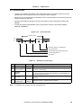
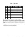
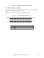
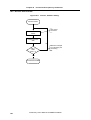
Chapter 1 Outline Description
Some host CPUs supports 2 instead of only 1 DCAN interface. Both interfaces, which have the same
functionality, are described at the same time in this manual. The reference is given by the index n
(n = 0, 1). Where necessary the registers of both DCAN interfaces are shown. Products that feature
only one DCAN interface refer to the first index (n = 0) only. For products with a single DCAN interface
the index in the register names needs to be omitted.
The address information for special function registers (SFR) and memory base addresses needs to be
picked up from the user manual of the particular product.
Remark:
The following indices were consequently used:
•
n = 0, 1
(for each of the 2 DCAN channels: DCAN0, DCAN1)
•
m = 2, 4
(address offset index for the 2 Mask Buffers)
•
r = 02 to 11
(address offset index for the 16 Receive Buffers)
•
t = 00, 01
(address offset index for the 2 Transmit Buffers)
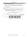
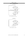
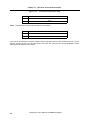
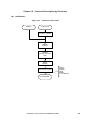
Figure 1-1:
Structural Block Diagram
CANL
CANH
CPU Access
Bus Arbitration Logic
Receive
Messages
Receive
Messages
Receive
Messages
Receive
Messages
CPU
SFR
Memory
Access
Engine
Transmit
Buffers
Transmit
Buffers
Interface
Management
High Speed
RAM
Memory
Buffer
RAM
(includes global registers)
CAN
Protocol
Time Stamp Signal
Timer
DCAN-Interface
External
Transceiver
This interface part handles all protocol activities by hardware in the CAN protocol part. The memory
access engine fetches information for the CAN protocol transmission from the dedicated RAM area to
the CAN protocol part or compares and sorts incoming information and stores it into predefined RAM
areas.
The DCAN interfaces directly to the RAM area that is accessible by the DCAN and by the CPU.
The DCAN part works with an external bus transceiver which converts the transmit data and receive
data lines to the electrical characteristics of the CAN bus itself.
Preliminary User’s Manual U14668EE3V0UM00
13
[MEMO]
14
Preliminary User’s Manual U14668EE3V0UM00
Chapter 2 CAN Protocol
CAN is an abbreviation of "Controller Area Network", and is a class C high speed multiplexed communication protocol. CAN is specified by Bosch in the CAN specification 2.0 from September 1991 and is
standardized in ISO-11898 (International Organization for Standardization) and SAE (Society of Automotive Engineers).
2.1 Protocol Mode Function
(1)
Standard format mode
• This mode supports an 11-bit message identifier thus making it possible to differentiate
between 2048 types of messages.
(2)
Extended format mode
• In the extended format mode, the identifier has 29 bits. It is built by the standard identifier (11
bits) and an extended identifier (18 bits).
• When the IDE bits of the arbitration field is "recessive", the frame is sent in the extended format
mode.
• When a message in extended format mode and a remote frame in standard format mode are
simultaneously transmitted, the node transmitting the message with the standard mode wins
the arbitration.
(3)
Bus values
• The bus can have one of two complementary logical values: "dominant" or "recessive". During
simultaneous transmission of "dominant" and "recessive" bits, the resulting bus value will be
"dominant" (non destructive arbitration).
• For example, in case of a wired-AND implementation of the bus, the "dominant" level would be
represented by a logical "0" and the "recessive" level by a logical 1. This specific representation
is used in this manual.
• Physical states (e.g. electrical voltage, light) that represent the logical levels are not given in this
document.
Preliminary User’s Manual U14668EE3V0UM00
15
Chapter 2
CAN Protocol
2.2 Message Format
The CAN protocol message supports different types of frames. The types of frames are listed below:
16
• Data frame:
Carries the data from a transmitter to the receiver.
• Remote frame:
Transmission demand frame from the requesting node.
• Error frame:
Frame sent on error detection.
• Overload frame:
Frame sent when a data or remote frame would be overwritten by the next
one before the receiving node could process it. The reception side did not
finish its operations on the reception of the previously received frame yet.
Preliminary User’s Manual U14668EE3V0UM00
Chapter 2 CAN Protocol
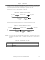
2.3 Data Frame / Remote Frame
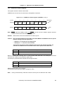
Figure 2-1:
R
D
1
(
)
Data Frame
Data frame
(11 + 1)
(29 + 3)
0 ... 64
6
16
2
7
3
) (
(
)
Bus idle
Interframe space
End of frame
ACK field
CRC field
Data field
Control field
Arbitration field
Start of frame
Figure 2-2:
Remote Frame
Remote frame
R
D
(
)
(
) (
)
Bus idle
Interframe space
End of frame
ACK field
CRC field
Control field
Arbitration field
Start of frame
Remark:
This frame is transmitted when the reception node requests transmission. Data field is not
transmitted even if the data length code ≠ '0' in the control field.
Preliminary User’s Manual U14668EE3V0UM00
17
Chapter 2
CAN Protocol
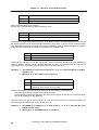
2.3.1 Description of each field
(1)
"R" indicates recessive level. "D" indicates dominant level.
Start of frame: The start of data frame and remote frame are indicated.
Figure 2-3:
Interframe space
on bus idle
Data Frame
Start of frame
Arbitration field
R
D
1 bit
• The start of frame (SOF) is denoted by the falling edge of the bus signal.
• Reception continues when 'Dominant level' is detected at the sample point.
• The bus becomes idle state when 'Recessive level' is detected at a sample point.
(2)
Arbitration field: Sets priority, specifies data frame or remote frame, and defines the protocol
mode.
Figure 2-4:
Arbitration Field/Standard Format Mode
Arbitration field
Control field
R
D
Identifier
ID28 . . . ID18
(11 bits)
18
RTR IDE r0
(1 bit) (1 bit)
Preliminary User’s Manual U14668EE3V0UM00
Chapter 2 CAN Protocol
Figure 2-5:
Arbitration Field/Extended Format Mode
Arbitration field
Control field
R
D
Identifier
ID28 . . . ID18
(11 bits)
SRR IDE
(1 bit) (1 bit)
Identifier
ID17 . . . ID0
(18 bits)
RTR r1
(1 bit)
r0
• ID28 - ID0 is the identifier.
• The identifier is transmitted with MSB at first position.
• Substitute Remote Request (SRR) is only used in extended format mode and is always
recessive.
Table 2-1:
Bit Number of the Identifier
Protocol Mode Identifier
Number
Standard format mode
11 bits
Extended format mode
29 bits
Table 2-2:
Frame Type
RTR Setting
RTR Bit
Data frame
0
Remote frame
1
Table 2-3:
Protocol Mode
Mode Setting
IDE Bit
Standard format mode
0
Extended format mode
1
Preliminary User’s Manual U14668EE3V0UM00
19
Chapter 2
(3)
CAN Protocol
Control field: The data byte number DLC in the data field specifies the number of databytes in the
current frame (DLC=0 to 8).
Figure 2-6:
Control Field (Standard Format Mode)
Control field
Arbitration field
Data field
R
D
RTR IDE
Figure 2-7:
r0
DLC3 DLC2DLC1DLC0
Control Field (Extended Format Mode)
Arbitration field
Data field
Control field
R
D
RTR
r0
r1
DLC3 DLC2DLC1DLC0
• The bits r0 and r1 are reserved bits for future use and are recommended to be recessive.
Table 2-4:
Data Length Code Setting
Data Length Code
Remark:
20
DLC3
DLC2
DLC1
DLC0
Number of Data Bytes
0
0
0
0
0
0
0
0
1
1
.
.
.
.
.
.
.
.
0
1
1
1
7
1
X
X
X
8
In case of a remote frame, the data field is not generated even if data length code ≠ '0'.
Preliminary User’s Manual U14668EE3V0UM00
Chapter 2 CAN Protocol
(4)
Data field: This field carries the data bytes to be sent. The number of data bytes is defined by the
DLC value.
Figure 2-8:
Control field
Data Field
Data field
CRC field
R
D
Data
(8 bits)
(5)
Data
(8 bits)
CRC field: This field consists of a 15-bit CRC sequence to check the transmission error and a
CRC delimiter.
Figure 2-9:
Data field and control field
CRC Field
CRC field
ACK field
R
D
CRC sequence CRC delimiter
(1 bit)
(15 bits)
• 15 bits CRC generation polynomial is expressed by
P(X) = X 15 + X 14 + X 10 + X 8 + X 7 + X 4 + X 3 + 1.
• Transmission node: Transmits the CRC sequence calculated from the start of frame, arbitration
field, control field and data field eliminating stuff bits.
• Reception node: The CRC received will be compared with the CRC calculated in the receiving
node. For this calculation the stuff bits of the received CRC are eliminated. In case these do not
match, the node issues an error frame.
Preliminary User’s Manual U14668EE3V0UM00
21
Chapter 2
(6)
CAN Protocol
ACK field: For check of normal reception.
Figure 2-10:
ACK Field
ACK field
CRC field
End of frame
R
D
ACK slot ACK delimiter
(1 bit)
(1 bit)
• Receive node sets the ACK slot to dominant level if no error was detected.
(7)
End of frame: Indicates the end of the transmission/reception.
Figure 2-11:
ACK field
R
D
22
End of frame
End of Frame
Interframe space of overload frame
(7 bits)
Preliminary User’s Manual U14668EE3V0UM00
Chapter 2 CAN Protocol
(8)
Interframe space: This sequence is inserted after data frames, remote frames, error frames, and
overload frames in the serial bitstream on the bus to indicate start or end of a frame. The length of
the interframe space depends on the error state (active or passive) of the node.
(a) Error active: Consists of 3 bits intermission and bus idle.
Figure 2-12:
Interframe Space/Error Active
Any frame
Any frame
Interframe space
R
D
Intermission
(3 bits)
Bus idle
(0 to ¥ bits)
(b) Error passive: Consists of 3 bits intermission, suspend transmission and bus idle.
Figure 2-13:
Interframe Space/Error Passive
Each frame
Each frame
Interframe space
R
D
Intermission
(3 bits)
Remark:
Suspend
transmission
(8 bits)
Bus idle
(0 to ¥ bits)
The nominal value of the intermission field is 3 bits. However, transmission nodes may start
immediately a transmission already in the 3rd bit of this field when a dominant level is
detected.
Table 2-5:
Error State
Operation in the Error State
Operation
Error active
Any node in this state is able to start a transmission whenever the bus is idle.
Error passive
Any node in this state has to wait for 11 consecutive recessive bits before initiating a
transmission.
Preliminary User’s Manual U14668EE3V0UM00
23
Chapter 2
CAN Protocol
2.4 Error Frame
• This frame is sent from a node if an error is detected.
• The type of an Error Frame is defined by its error flag: ACTIVE ERROR FLAG or PASSIVE
ERROR FLAG. Which kind of flag a node transmits after detecting an error condition depends
on the internal count of the error counters of each node.
Figure 2-14:
Error Frame
Error frame
R
D
(
)
(
)
Interframe space or overload frame
Error delimiter
Error flag
Error flag
Error bit
Table 2-6:
No.
24
Name
1
Error flag
2
Error flag
superpositioning
3
Bit Number
6
Definition of each Field
Definition
Error active node: sends 6 bits dominant level continuously.
Error passive node: sends 6 bits recessive level continuously.
0 to 6
Nodes receiving an “error flag” detect bit stuff errors and issue error
flags’ themselves.
Error delimiter
8
Sends 8 bits recessive level continuously.
In case of monitoring dominant level at 8th bit, an overload frame is
transmitted after the next bit.
4
Erroneous bit
-
An error frame is transmitted continuously after the bit where the error
has occurred (in case of a CRC error, transmission continues after
the ACK delimiter).
5
Interframe space/
overload frame
3/14
20 MAX
Interframe space or overload frame continues.
Preliminary User’s Manual U14668EE3V0UM00
Chapter 2 CAN Protocol
2.5 Overload Frame
• This frame is started at the first bit of the intermission when the reception node is busy with
exploiting the receive operation and is not ready for further reception.
• When a bit error is detected in the intermission, also an overload frame is sent following the next
bit after the bit error detection.
• Detecting a dominant bit during the 3rd bit of intermission will be interpreted as START OF
FRAME.
• At most two OVERLOAD FRAMEs may be generated to delay the next DATA FRAME or
REMOTE FRAMENote.
Figure 2-15:
Overload Frame
Overload frame
R
D
(
)
(
)
Interframe space or overload frame
Overload delimiter
Overload flag superpositioning (Node n)
Overload flag (Node m)
Each frame
Table 2-7:
No.
Name
Definition of each Frame
Bit Number
Definition
1
Overload flag
6
2
Overload flag
from any node
0 to 6
3
Overload
delimiter
8
Sends 8 bits recessive level continuously.
In case of monitoring dominant level at 8th bit, an overload frame is
transmitted after the next bit.
4
Any frame
-
Output following the end of frame, error delimiter and overload
delimiter.
5
Interframe space/
overload frame
3/14
20 MAX
Sent 6 bits dominant level continuously.
A node that receives an overload flag in the interframe space.
Issues an overload flag.
Interframe space or overload frame continues.
Note: The DCAN never needs to send an overload frame.
Preliminary User’s Manual U14668EE3V0UM00
25
[MEMO]
26
Preliminary User’s Manual U14668EE3V0UM00
Chapter 3 Function
3.1 Arbitration
If two or more nodes happen to start transmission in coincidence, the access conflict is solved by a bitwise arbitration mechanism during transmission of the ARBITRATION FIELD.
(1)
When a node starts transmission:
• During bus idle, the node having the output data can transmit.
(2)
When more than one node starts transmission:
• The node with the lower identifier wins the arbitration.
• Any transmitting node compares its output arbitration field and the data level on the bus.
• It looses arbitration, when it sends recessive level and reads dominant from bus.
Table 3-1:
Level Detection
(3)
Arbitration
Status of Arbitrating Node
Conformity of Level
Continuous Transmission
Non-conformity of
level
The data output is stopped from the next bit and reception operation starts.
Priority of data frame and remote frame:
• When a data frame and remote frame with the same message identifier are on the bus, the data
frame has priority because its RTR bit carries 'Dominant level'. The data frame wins the
arbitration.
Preliminary User’s Manual U14668EE3V0UM00
27
Chapter 3
Function
3.2 Bit Stuffing
When the same level continues for more than 5 bits, bit stuffing (insert 1 bit with inverse level) takes
place.
• Due to this a resynchronization of the bit timing can be done at least every 10 bits.
• Nodes detecting an error condition send an error frame, violating the bit stuff rule and indicating
this message to be erroneous for all nodes.
Table 3-2:
Bit Stuffing
Transmission
During the transmission of a data frame and a remote frame, when the same level continues
for 5 bits in the data between the start of frame and the ACK field, 1 bit level with reverse level
of data is inserted before the following bit.
Reception
During the reception of a data frame and a remote frame, when the same level continues for
5 bits in the data between the start of frame and the ACK field, the reception is continued by
deleting the next bit.
3.3 Multi Master
As the bus priority is determined by the identifier, any node can be the bus master.
3.4 Multi Cast
Any message can be received by any node (broadcast).
3.5 Sleep Mode/Stop Function
This is a function to put the CAN controller in waiting mode to achieve low power consumption. The
SLEEP mode of the DCAN complies to the method described in ISO 11898.
Additional to this SLEEP mode, which can be woken up by bus activities, the STOP mode is fully controlled by the CPU device.
28
Preliminary User’s Manual U14668EE3V0UM00
Chapter 3 Function
3.6 Error Control Function
(1)
Error types
Table 3-3:
Error Types
Description of Error
Type
Detection State
Detection Method
Detection
Condition
Transmission/
Reception
Field/Frame
Bit error
Comparison of output
level and level on the bus
(except stuff bit)
Disagreement
of both levels
Transmission/
reception node
Bit that output data on the bus at the
start of frame to the end of frame,
error frame and overload frame.
Stuff error
Check of the reception
data at the stuff bit
6 consecutive
bits of the
same output
level
Transmission/
reception node
Start of frame to CRC sequence
CRC error
Comparison of the CRC
generated from the
reception data and the
received CRC sequence
Disagreement
of CRC
Reception node Start of frame to data field
Form
error
Field/frame check of the
fixed format
Detection of
the fixed format error
CRC delimiter
ACK field
Reception node End of frame
Error frame
Overload frame
ACK error
Check of the ACK slot by
the transmission node
Detection of
recessive
level in ACK
slot
Transmission
node
(2)
Output timing of the error frame
Table 3-4:
Type
(3)
ACK slot
Output Timing of the Error Frame
Output timing
Bit error, stuff error,
form error, ACK error
Error frame is started at the next bit timing following the detected error
Error passive
CRC error Error frame is started at the next bit timing following the ACK delimiter
Measures when error occurs
• Transmission node re-transmits the data frame or the remote frame after the error frame.
• The CAN standard (ISO-11898) allows a programmable suppression of this re-transmission. It
is called single shot mode.
Preliminary User’s Manual U14668EE3V0UM00
29
Chapter 3
(4)
Function
Error state
(a) Types of error state
• Three types of error state: These are error active, error passive and bus off.
• The transmission error counter (TEC) and the reception error counter (REC) control the error
state.
• The error counters are incremented on each error occurrence (refer to Table 3-6).
• If the value of error counter exceeds 96, warning level for error passive state is reached.
• When only one node is active at start-up, it may not receive an acknowledgment on a
transmitted message. This will increment TEC until error passive state is reached. The bus off
state will not be reached because for this specific condition TEC will not increment any more if
values greater than 127 are reached.
• A node in bus off state will not issue any dominant level on the CAN transmit pin. The reception
of messages is not affected by the bus off state.
Table 3-5:
Type
Error active
Error passive
Bus off
30
Operation
Value of Error Counter
Transmission/
reception
0 to 127
Transmission
128 to 255
Reception
Transmission
Reception
Types of Error
128 or more
more than 255
-
Output Error Flag Type
Active error flag (6 bits of dominant level continue)
Passive error flag (6 bits of recessive level continue)
Communication cannot be made
Does not exist
Preliminary User’s Manual U14668EE3V0UM00
Chapter 3 Function
(b) Error counter
• Error counter counts up when an error has occurred, and counts down upon successful
transmission and reception. The error counters are updated during the first bit of an error flag.
Table 3-6:
Error Counter
Transmission Error
Counter (TEC)
Reception Error
Counter (REC)
Reception node detects an error (except bit error in the active
error flag or overload flag).
No change
+1
Reception node detects dominant level following the error flag
of the own error frame.
No change
+8
Transmission node transmits an error flag.
Exception:
1. ACK error is detected in the error passive state and dominant level is not detected in the passive error flag sent.
2. Stuff error generation in arbitration field.
+8
No change
Bit error detection during active error flag and overload flag
when transmitting node is in error active state.
+8
No change
Bit error detection during active error flag and overload flag
when receiving node is in error active state.
No change
+8
+8
+8
When the transmitting node has completed to sent without
error.
-1
(-0 when
error counter = 0)
No change
When the reception node has completed to receive without
error.
No change
-1 (1 ≤REC ≤127)
–0 (REC = 0)
119-127 (REC > 127)
State
When the node detects fourteen continuous dominant bits
counted from the beginning of the active error flag or the overload flag, and every time, eight subsequent dominant bits after
that are detected.
Every time when the node detects eight continuous dominant
bits after the passive error flag.
(c) Overload frame
• In case the recessive level of first intermission bit is driven to dominant level, an overload frame
occurs on the bus. Upon detection of an overload frame any transmit request will be postponed
until the bus becomes idle.
Preliminary User’s Manual U14668EE3V0UM00
31
Chapter 3
Function
3.7 Baud Rate Control Function
(1)
Nominal bit time (8 to 25 time quanta)
• Definition of 1 data bit time is as follows.
Figure 3-1:
Nominal Bit Time (8 to 25 Time Quanta)
Nominal bit time
Sync
segment
Prop
segment
Phase
segment 1
Phase
segment 2
SJW
SJW
Sample point
[1 Minimum time for one time/quantum (TQ) = 1/fx]
• Sync segment: In this segment the bit synchronization is performed.
• Prop segment: This segment absorbs delays of the output buffer, the CAN bus and the input
buffer. Prop segment time =(output buffer delay) + (CAN bus delay) + (input buffer delay).
• Phase segment 1/2: These segments compensate the data bit time error. The larger the size
measured in TQ is, the larger is the tolerable error.
• The synchronization jump width (SJW) specifies the synchronization range. The SJW is
programmable. SJW can have less or equal number of TQ as phase segment 2.
Table 3-7:
Segment Name and Segment Length
Segment Name
Sync segment
(Synchronization segment)
Segment Length
(allowed Number of TQs)
1
Prop segment
(Propagation segment)
Programmable 1 to 8
Phase segment 1
(Phase buffer segment 1)
Programmable 1 to 8
Phase segment 2
(Phase buffer segment 2)
Maximum of phase segment 1
and the IPT Note
SJW
Programmable 1 to 4
Note: IPT = Information Processing Time. It needs to be less than or equal to 2 TQ.
32
Preliminary User’s Manual U14668EE3V0UM00
Chapter 3 Function
(2)
Adjusting synchronization of the data bit
• The transmission node transmits data synchronized to the transmission node bit timing.
• The reception node adjusts synchronization at recessive to dominant edges on the bus.
Depending on the protocol this synchronization can be a hard or soft synchronization.
(a) Hard synchronization
This type of synchronization is performed when the reception node detects a start of frame in the bus
idle state.
• When the node detects a falling edge of a SOF, the current time quanta becomes the
synchronization segment. The length of the following segments are defined by the values
programmed into the SYNC0 and SYNC1 registers.
Figure 3-2:
Adjusting Synchronization of the Data Bit
Bus idle
Start of frame
CAN bus
Bit timing
Sync
segment
Prop
segment
Phase
segment 1
Phase
segment 2
Preliminary User’s Manual U14668EE3V0UM00
33
Chapter 3
Function
(b) Soft synchronization
When a recessive to dominant level change on the bus is detected, a soft synchronization is performed.
• If the phase error is larger than the programmed SJW value, the node will adjust the timing by
applying this SJW-value. Full synchronization is achieved by subsequent adjustments on the
next recessive to dominant edge(s).
• These errors that are equal or less of the programmed SJW are corrected instantly and full
synchronization is achieved already for the next bit.
• The TQ at which the edge occurs becomes sync segment forcibly if the phase error is less than
or equal to SJW.
Figure 3-3:
Bit Synchronization
Phase
segment
Sync
segment
Prop
segment
-SJW
Phase
segment 2
Sync
segment
Prop
segment
+SJW
34
Preliminary User’s Manual U14668EE3V0UM00
Chapter 3 Function
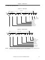
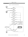
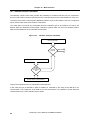
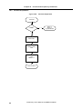
3.8 State Shift Chart
Figure 3-4:
Transmission State Shift Chart
Reception
C
Start of frame
End
Bit error
Arbitration field
A
Reception
RTR = 1
Control field
Bit error
RTR = 0
Data field
Bit error
End
CRC field
Bit error
End
ACK field
ACK error
End
End of frame
End
Intermission 1
Error passive
Bit error
Error frame
End
Bit error
Bit error
Form error
Overload frame
End
Error active
Initialization setting
Intermission 2
8 bits of '1'
Start of frame reception
B
Bus idle
Start of frame transmission
Reception
Preliminary User’s Manual U14668EE3V0UM00
35
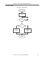
Chapter 3
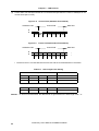
Figure 3-5:
Function
Reception State Shift Chart
Transmission
B
Start of frame
Transmission
End
A
Stuff error
Arbitration field
RTR = 1
Stuff error
Control field
RTR = 0
Data field
Stuff error
End
CRC field
CRC error, stuff error
End
ACK field
ACK error, bit error
End
End of frame
Bit error, form error
Error frame
End
End
Intermission 1
Not ready
Not ready
Bit error
Form error
Overload frame
End
Initialization setting
Start of frame transmission
C
Bus idle
Start of frame reception
Transmission
36
Preliminary User’s Manual U14668EE3V0UM00
Chapter 3 Function
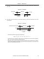
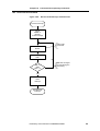
Figure 3-6:
Error State Shift Chart
(a) Transmission
Error active
TEC >
TEC < 127
128
Error passive
TEC
>
256
Bus off
TEC = 0
TEC = Transmission error counter
(b) Reception
Error active
REC > 128
Error passive
REC < 127
REC = Reception error counter
Preliminary User’s Manual U14668EE3V0UM00
37
[MEMO]
38
Preliminary User’s Manual U14668EE3V0UM00
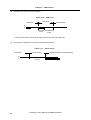
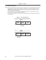
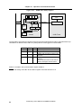
Chapter 4
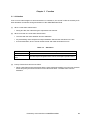
Connection with Target System
The DCAN Macro has to be connected to the CAN bus with an external transceiver.
Figure 4-1:
Connection to the CAN Bus
CTxD
DCAN Macro
CRxD
CANL
Transceiver
Preliminary User’s Manual U14668EE3V0UM00
CANH
39
Chapter 5
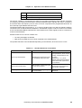
DCAN Controller Configuration
The DCAN-module consists of the following hardware
.
Item
Remark:
Configuration
Message definition
In RAM area
DCAN input/output
1 (CTXD1n)
1 (CRXD1n)
Control registers
DCAN control register (DCANCn)Note
CAN control register (CANCn)
Transmit control register (TCRn)
Receive message register (RMESn)
Redefinition control register (REDEFn)
DCAN error status register (CANESn)
Transmit error counter (TECn)
Receive error counter (RECn)
Message count register (MCNTn)
Bit rate prescaler (BRPRSn)
Synchronous control register 0 (SNYC0n)
Synchronous control register 1 (SYNC1n)
Mask control register (MASKCn)
n = 0, 1
Note: The register(s) DCANCn is/are not available on all products.
40
Preliminary User’s Manual U14668EE3V0UM00
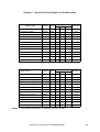
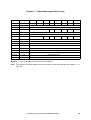
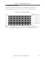
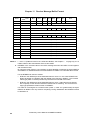
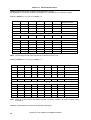
Chapter 6 Special Function Register for DCAN-module
Register Name
Symbol
R/W
DCAN control register
DCANC0
CAN control register
After Reset
1 Bit
8 Bit
16 Bit
R/W
×
×
-
00H
CANC0
R/W
×
×
-
01H
Transmit control register
TCR0
R/W
-
×
-
00H
Receive message register
RMES0
R
-
×
-
00H
Redefinition control register
REDEF0
R/W
×
×
-
00H
DCAN error status register
CANES0
R/W
-
×
-
00H
Transmit error counter
TEC0
R
-
×
-
00H
Receive error counter
REC0
R
-
×
-
00H
Message count register
MCNT0
R
-
×
-
C0H
Bit rate prescaler
BRPRS0
R/W
-
×
-
00H
Synchronous control register 0
SYNC00
R/W
-
×
-
18H
Synchronous control register 1
SYNC10
R/W
-
×
-
0EH
Mask control register
MASKC0
R/W
-
×
-
00H
Symbol
R/W
DCAN control register
DCANC1
CAN control register
Register Name
Remark:
Bit Manipulation Units
Bit Manipulation Units
After Reset
1 Bit
8 Bit
16 Bit
R/W
×
×
-
00H
CANC1
R/W
×
×
-
01H
Transmit control register
TCR1
R/W
-
×
-
00H
Receive message register
RMES1
R
-
×
-
00H
Redefinition control register
REDEF1
R/W
×
×
-
00H
DCAN error status register
CANES1
R/W
-
×
-
00H
Transmit error counter
TEC1
R
-
×
-
00H
Receive error counter
REC1
R
-
×
-
00H
Message count register
MCNT1
R
-
×
-
C0H
Bit rate prescaler
BRPRS1
R/W
-
×
-
00H
Synchronous control register 0
SYNC01
R/W
-
×
-
18H
Synchronous control register 1
SYNC11
R/W
-
×
-
0EH
Mask control register
MASKC1
R/W
-
×
-
00H
The registers DCANCn are not available on every host CPU.
Preliminary User’s Manual U14668EE3V0UM00
41
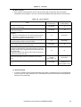
Chapter 6 Special Function Register for DCAN-module
The following SFR bits can be accessed with 1-bit instructions. The other SFR registers have to be
accessed with 8-bit instructions.
Name
42
Description
Bit
DCANEN
Enable/Disable DCANn
DCANCn.0
SOFE
Start of frame enable
CANCn.4
SLEEP
Sleep mode
CANCn.2
INIT
Initialize
CANCn.0
DEF
Redefinition enable
REDEFn.7
Preliminary User’s Manual U14668EE3V0UM00
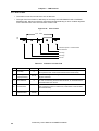
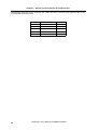
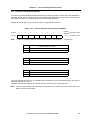
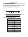
Chapter 7 Message Buffer Configuration
Address Offset Note 2
Register Name
000H to 00FH
Transmit buffer 0
010H to 01FH
Transmit buffer 1
020H to 02FH
Receive buffer 0 / Mask 0
030H to 03FH
Receive buffer 1
040H to 04FH
Receive buffer 2 / Mask 1
050H to 05FH
Receive buffer 3
060H to 06FH
Receive buffer 4
070H to 07FH
Receive buffer 5
080H to 08FH
Receive buffer 6
090H to 09FH
Receive buffer 7
0A0H to 0AFH
Receive buffer 8
0B0H to 0BFH
Receive buffer 9
0C0H to 0CFH
Receive buffer 10
0D0H to 0DFH
Receive buffer 11
0E0H to 0EFH
Receive buffer 12
0F0H to 0FFH
Receive buffer 13
100H to 10FH
Receive buffer 14
110H to 11FH
Receive buffer 15
R/W
After Reset
R/W
undefinedNote1
Notes: 1. Contents is undefined, because data resides in normal RAM area.
2. This address is an offset to the RAM area starting address which is fixed. Depending on the
product, the offset address is selectable by the CADDx bits (x = 0, 1) in the message count
register(s) (MCNTn) or the offset is fixed by the design of the hardware and the setting of
CADDx in MCNTn has no influence.
Some products feature 14 receive buffers only.
Preliminary User’s Manual U14668EE3V0UM00
43
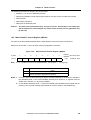
Chapter 8
Transmit Buffer Structure
Each DCAN channel has 2 independent transmit buffers. The two buffers have a 16 byte data structure
for standard and extended frames with the ability to send up to 8 data bytes per message. The structure
of the transmit buffer is similar to the structure of the receive buffers. The CPU can use addresses that
are specified as “unused” in the transmit buffer layout. As well the CPU may use unused ID addresses,
unused data addressesNote, and an unused transmit buffer of the DCAN for its own purposes. The control bits, the identification and the message data has to be stored in the message RAM area.
The transmission control is done by the TCRn register. A transmission priority selection allows the customer to realize an application specific priority selection. After the priority selection the transmission
can be started by setting the TXRQx bit (x = 0, 1).
In the case that both transmit buffers are used, the transmit priorities can be set. For this purpose the
DCAN has the TXP bit in the TCRn register (n = 0, 1). The application software has to set this priority
before the transmission is started. The two transmit buffers of each DCAN channel (DCAN0, DCAN1)
supply two independent interrupt lines for an interrupt controller.
Note: Message objects that need less than 8 data byte (DLC < 8) may use the remaining bytes
(8 - DLC) for application purposes.
44
Preliminary User’s Manual U14668EE3V0UM00
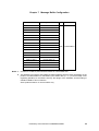
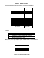
Chapter 9 Transmit Message Buffer Format
Name
AddressNote
Bit 7
Bit 6
Bit 5
Bit 4
Bit 3
Bit 2
Bit 1
Bit 0
TCON
t0H
IDE
RTR
0
0
DLC3
DLC2
DLC1
DLC0
0
0
0
0
0
0
t1H
Unused
IDTX0
t2H
ID standard part
IDTX1
t3H
IDTX2
t4H
ID extended part
IDTX3
t5H
ID extended part
IDTX4
t6H
ID standard part
ID extended part
0
0
0
0
0
t7H
Unused
DATA0
t8H
Message data byte 0
DATA1
t9H
Message data byte 1
DATA2
tAH
Message data byte 2
DATA3
tBH
Message data byte 3
DATA4
tCH
Message data byte 4
DATA5
tDH
Message data byte 5
DATA6
tEH
Message data byte 6
DATA7
tFH
Message data byte 7
Remark:
t = 00, 01 (address index for the 2 transmit buffers)
Note: This address is a relative offset to the starting address of the transmit buffer (see Chapter 7
page 43).
Preliminary User’s Manual U14668EE3V0UM00
on
45
Chapter 9 Transmit Message Buffer Format
9.1 Transmit Message Definition
The memory location labelled TCON includes the information of the RTR bit and the bits of the control
field of a data or remote frame.
TCON is set with a 1-bit or an 8-bit memory manipulation instruction.
Figure 9-1:
Transmit Message Definition Register (TCON)
Symbol
7
6
5
4
3
2
1
0
TCON
IDE
RTR
0
0
DLC3
DLC2
DLC1
DLC0
Note: t = 00, 01 (address index for the 2 transmit buffers, see Chapter 7
IDE
t0H
undefined R/W
on page 43).
Identifier Extension Select
0
Transmit standard frame message; 11 bit identifier
1
Transmit extended frame message; 29 bit identifier
RTR
Remote Transmission Select
0
Transmit data frames
1
Transmit remote frames
DLC3
DLC2
DLC1
DLC0
Data Length Code Selection of
Transmit MessageNote
0
0
0
0
0 data bytes
0
0
0
1
1 data bytes
0
0
1
0
2 data bytes
0
0
1
1
3 data bytes
0
1
0
0
4 data bytes
0
1
0
1
5 data bytes
0
1
1
0
6 data bytes
0
1
1
1
7 data bytes
1
0
0
0
8 data bytes
Others than above
Remark:
AddressAfter Reset R/W
offsetNote
Note
The control field describes the format of frame that is generated and its length. The
reserved bits of the CAN protocol are always sent in dominant state (0).
Note: The data length code selects the number of bytes which have to be transmitted. Valid entries for
the data length code (DLC) are 0 to 8. If a value greater than 8 is selected, 8 bytes are
transmitted in the data frame. The Data Length Code is specified in DLC3 through DLC0.
46
Preliminary User’s Manual U14668EE3V0UM00
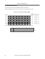
Chapter 9 Transmit Message Buffer Format
9.2 Transmit Identifier Definition
These memory locations set the message identifier in the arbitration field of the CAN protocol.
IDTX0 to IDTX4 register can be set with a 1-bit or an 8-bit memory manipulation instruction.
Figure 9-2:
Transmit Identifier Register
AddressAfter Reset R/W
offsetNote
Symbol
7
6
5
4
3
2
1
0
IDTX0
ID28
ID27
ID26
ID25
ID24
ID23
ID22
ID21
t2H
undefined R/W
IDTX1
ID20
ID19
ID18
0
0
0
0
0
t3H
undefined R/W
IDTX2
ID17
ID16
ID15
ID14
ID13
ID12
ID11
ID10
t4H
undefined R/W
IDTX3
ID9
ID8
ID7
ID6
ID5
ID4
ID3
ID2
t5H
undefined R/W
IDTX4
ID1
ID0
0
0
0
0
0
0
t6H
undefined R/W
Note: t = 00, 01 (address index for the 2 transmit buffers, see Chapter 7
Remark:
on page 43)
If a standard frame is defined by the IDE bit in the TCON register then IDTX0 and IDTX1 are
used only. IDTX2 to IDTX4 are free for use by the CPU for application needs then.
Preliminary User’s Manual U14668EE3V0UM00
47
Chapter 9 Transmit Message Buffer Format
9.3 Transmit Data Definition
These memory locations set the transmit message data of the data field in the CAN frame.
DATA0 to DATA7 can be set with a 1-bit or an 8-bit memory manipulation instruction.
Figure 9-3:
Symbol
7
6
5
4
3
Transmit Data
2
1
AddressAfter Reset R/W
offsetNote
0
DATA0
t8H
undefined R/W
DATA1
t9H
undefined R/W
DATA2
tAH
undefined R/W
DATA3
tBH
undefined R/W
DATA4
tCH
undefined R/W
DATA5
tDH
undefined R/W
DATA6
tEH
undefined R/W
DATA7
tFH
undefined R/W
Note: t = 00, 01 (address index for the 2 transmit buffers, see Chapter 7
Remark:
48
on page 43).
Unused data bytes that are not used by the definition in the DLC bits in the TCON byte are
free for use by the CPU for application needs.
Preliminary User’s Manual U14668EE3V0UM00
Chapter 10
Receive Buffer Structure
The DCAN has up to 16 receive buffers. The number of used buffers is defined by the MCNTn register.
Unused receive buffers can be used as application RAM for the CPU. The received data is stored
directly in this RAM area.
The 16 buffers have a 16 byte data structure for standard and extended frames with a capacity of up to
8 data bytes per message. The structure of the receive buffer is similar to the structure of the transmit
buffers. The semaphore bits DN and MUC enable a secure reception detection and data handling. For
the first 8 receive message buffers the successful reception is mirrored by the DN-flags in the RMESn
register.
The receive interrupt request can be enabled or disabled for each used buffer separately.
Preliminary User’s Manual U14668EE3V0UM00
49
Chapter 11 Receive Message Buffer Format
Addressoffset Note1
Bit 7
Bit 6
Bit 5
Bit 4
Bit 3
Bit 2
Bit 1
Bit 0
IDCON
r0H
0
0
0
0
0
ENI
RTR
IDE
DSTAT
r1H
DN
MUC
R1
R0
IDREC0
r2H
IDREC1
r3H
IDREC2
r4H
ID extended part
IDREC3
r5H
ID extended part
IDREC4
r6H
Name
DLC
ID standard part
ID standard part
ID extended part
0
0
0
0
0
0
0
r7H
unused
DATA0
r8H
Message data byte 0
DATA1
r9H
Message data byte 1
DATA2
rAH
Message data byte 2
DATA3
rBH
Message data byte 3
DATA4
rCH
Message data byte 4
DATA5
rDH
Message data byte 5
DATA6
rEH
Message data byte 6
DATA7
rFH
Message data byte 7
0
RTRREC Note2
0
0
Notes: 1. r = 02 to 11 (address index for the 16 Receive Buffers, see Chapter 7
relative offset to the start address of the receive buffer.
on page 43); it is a
2. RTRREC is the received value of the RTR message bit when this buffer is used together
with a mask function.
By using the mask function a successfully received identifier overwrites the bytes IDREC0
and IDREC1 for standard frame format and IDREC0 to IDREC4 for extended frame format.
For the RTRREC bit exist two modes:
•
RTR bit in the MCON byte of the dedicated mask is set to 0. In this case RTRREC will
always be written to 0 together with the update of the IDn bits in IDREC1. The received
frame type (data or remote) is defined by the RTR bit in IDCON of the buffer.
•
RTR bit in the MCON byte of the dedicated mask is set to 1 (data and remote frames
are accepted). In this case the RTR bit in IDCON has no meaning. The received message type passed the mask is shown in RTRREC.
If a buffer is not assigned to a mask function (mask 1, mask 2 or global mask) the bytes
IDREC0 to IDREC4 are only read for comparing. During initialization the RTRREC should
be defined to 0.
50
Preliminary User’s Manual U14668EE3V0UM00
Chapter 11
Receive Message Buffer Format
11.1 Receive Control Bits Definition
The memory location labelled IDCON defines the kind of frame (data or remote frame with standard or
extended format) that is monitored for the associated buffer. Notification by the receive interrupt upon
successful reception can be selected for each receive buffer separately.
IDCON can be set with a 1-bit or an 8-bit memory manipulation instruction.
Figure 11-1:
Receive Identifier Control Register (IDCON)
Symbol
7
6
5
4
3
2
1
0
IDCON
0
0
0
0
0
ENI
RTR
IDE
Note: r = 02 to 11 (address index for the 16 Receive Buffers, see Chapter 7
ENI
AddressAfter Reset R/W
offsetNote
r0H
on page 43).
Enable Interrupt on ReceiveNote
0
No interrupt generated
1
Generate receive interrupt after reception of valid message
RTR
Remote Transmission Select
0
Receive data frames
1
Receive remote frames
IDE
undefined R/W
Identifier Extension Select
0
Receive standard frame message; 11 bit identifier
1
Receive extended frame message; 29 bit identifier
The control bits define the type of message that is transferred in the associated buffer if this type of
message appears on the bus.
This byte will never be written by the DCAN. Only the host CPU can change this byte.
Note: The user has to define with the ENI bit if he wants to set a receive interrupt request when new
data is received in this buffer.
Preliminary User’s Manual U14668EE3V0UM00
51
Chapter 11 Receive Message Buffer Format
11.2 Receive Status Bits Definition
The memory location labelled DSTAT sets the receive status bits of the arbitration field of the CAN
protocol.
DSTAT can be set with a 1-bit or an 8-bit memory manipulation instruction.
Figure 11-2:
Receive Status Bits Register (DSTAT)
Symbol
7
6
5
4
3
2
1
0
DSTAT
DN
MUC
R1
R0
DLC3
DLC2
DLC1
DLC0
Note: r = 02 to 11 (address index for the 16 Receive Buffers, see Chapter 7
AddressAfter Reset R/W
offsetNote
r1H
undefined R/W
on page 43).
The receive status reflects the current status of a message. It signals whether new data is stored or if
the DCAN currently transfers data into this buffer.
In addition the data length of the last transferred data and the reserved bits of the protocol are shown.
DN
Data New
0
No change in data
1
Data changed
The DCAN-module sets DNn twice. At first when it starts storing a message from the shadow buffer into
the receive buffer and secondly when it finished the operation.
The CPU needs to clear this bit, to signal by itself that it has read the data. During initialisation of the
receive buffers the DNn bit should also be cleared. Otherwise the CPU gets no information on an
update of the buffer after a successful reception.
MUC
Memory Update
0
CAN does not access data part
1
CAN is transferring new data to message buffer
The DCAN-module sets MUC when it starts transferring a message into the buffer and clears the MUC
bit when the transfer is finished.
R1
0
Reserved bit 1 of received message was “0”
1
Reserved bit 1 of received message was “1”
R0
52
Reserved Bit 1
Reserved Bit 0
0
Reserved bit 0 of received message was “0”
1
Reserved bit 0 of received message was “1”
Preliminary User’s Manual U14668EE3V0UM00
Chapter 11
Receive Message Buffer Format
Data Length Code Selection
of Receive Message
DLC3
DLC2
DLC1
DLC0
0
0
0
0
0 data bytes
0
0
0
1
1 data bytes
0
0
1
0
2 data bytes
0
0
1
1
3 data bytes
0
1
0
0
4 data bytes
0
1
0
1
5 data bytes
0
1
1
0
6 data bytes
0
1
1
1
7 data bytes
1
0
0
0
8 data bytes
Others than above
Note
DSTAT is written by the DCAN two times during message storage:
At the first access to this buffer DN = 1, MUC = 1, reserved bits and DLCx (x = 3 to 0) are written.
At the last access to this buffer DN = 1, MUC = 0, reserved bits and DLCx (x = 3 to 0) are written.
Note: Valid entries for the data length code are 0 to 8. If a value higher than 8 is received, 8 bytes are
stored in the message buffer frame together with the data length code received in the DLC of
the message.
Preliminary User’s Manual U14668EE3V0UM00
53
Chapter 11 Receive Message Buffer Format
11.3 Receive Identifier Definition
These memory locations define the receive identifier of the arbitration field of the CAN protocol.
IDREC0 to IDREC4 can be set with a 1-bit or an 8-bit memory manipulation instruction.
Figure 11-3:
Receive Identifier Register
AddressAfter Reset R/W
offsetNote
Symbol
7
6
5
4
3
2
1
0
IDREC0
ID28
ID27
ID26
ID25
ID24
ID23
ID22
ID21
r2H
undefined R/W
IDREC1
ID20
ID19
ID18
0
0
0
0
RTRREC
r3H
undefined R/W
IDREC2
ID17
ID16
ID15
ID14
ID13
ID12
ID11
ID10
r4H
undefined R/W
IDREC3
ID9
ID8
ID7
ID6
ID5
ID4
ID3
ID2
r5H
undefined R/W
IDREC4
ID1
ID0
0
0
0
0
0
0
r6H
undefined R/W
Note: r = 02 to 11 (address index for the 16 Receive Buffers, see Chapter 7
on page 43).
The identifier of the receive message has to be defined during the initialization of the DCAN.
The DCAN uses this data for the comparison with the identifiers received on the CAN bus. For normal
message buffers without mask function this data is only read by the DCAN for comparison. In combination with a mask function this data is overwritten by the received ID that has passed the mask.
The identifier of the receive messages should not be changed without being in the initialization phase or
setting the receive buffer to redefinition in the RDEF register, because the change of the contents can
happen at the same time when the DCAN uses the data for comparison. This can cause inconsistent
data stored in this buffer and also the ID-part can be falsified in case of using mask function.
Remarks: 1. The unused parts of the identifier (IDREC1 bit 4 - 0 always and IDREC4 bit 5 - 0 in case
of extended frame reception) may be written by the DCAN to “0”. They are not released
for other use by the CPU.
2. RTRREC is the received value of the RTR message bit when this buffer is used together
with a mask function.
By using the mask function a successfully received identifier overwrites the bytes
IDREC0 and IDREC1 registers for standard frame format and IDREC0 to IDREC4
registers for extended frame format. For the RTRREC bit exists two modes:
•
RTR bit in the MCON register of the dedicated mask is set to “0”. In this case
RTRREC bit will always be written to “0” together with the update of the IDx bits (x =
18 to 20) in IDREC1. The received frame type (data or remote) is defined by the
RTR bit in IDCON of the buffer.
•
RTR bit in the MCON byte of the dedicated mask is set to “1” (data and remote
frames are accepted). In this case the RTR bit in IDCON register has no meaning.
The received message type passed the mask is shown in RTRREC bit.
If a buffer is not dedicated to a mask function (mask 1, mask 2 or global mask) the
IDREC0 to IDREC4 registers are only read for comparing. All receive identifiers should
be defined to “0” before the application sets up its specific values.
54
Preliminary User’s Manual U14668EE3V0UM00
Chapter 11
Receive Message Buffer Format
11.4 Receive Message Data Part
These memory locations set the receive message data part of the CAN protocol.
DATA0 to DATA7 can be set with a 1-bit or an 8-bit memory manipulation instruction.
Figure 11-4:
Symbol
7
6
5
4
3
Receive Data
2
1
0
AddressAfter Reset R/W
offsetNote
DATA0
r8H
undefined R/W
DATA1
r9H
undefined R/W
DATA2
rAH
undefined R/W
DATA3
rBH
undefined R/W
DATA4
rCH
undefined R/W
DATA5
rDH
undefined R/W
DATA6
rEH
undefined R/W
DATA7
rFH
undefined R/W
Note: r = 02 to 11 (address index for the 16 Receive Buffers, see Chapter 7
on page 43).
The DCAN stores received data bytes in this memory area. Only those data bytes which are actually
received and match with the identifier are stored in the receive buffer memory area.
If the DLC is less than eight, the DCAN will not write additional bytes exceeding the DLC value up to
eight. The DCAN stores a maximum of 8 bytes (according to the CAN protocol rules) even when the
received DLC is greater than eight.
Preliminary User’s Manual U14668EE3V0UM00
55
[MEMO]
56
Preliminary User’s Manual U14668EE3V0UM00
Chapter 12 Mask Function
Table 12-1:
Name
Addressoffset Note
MCON
m0H
Bit 7
Mask Function Register
Bit 6
Bit 5
Bit 4
Bit 3
Bit 2
Bit 1
Bit 0
RTR
m1H
Unused
MREC0
m2H
ID standard part
MREC1
m3H
MREC2
m4H
ID extended part
MREC3
m5H
ID extended part
MREC4
m6H
ID standard part
ID extended part
0
0
0
m7H
Unused
m8H
Unused
m9H
Unused
mAH
Unused
mBH
Unused
mCH
Unused
mDH
Unused
mEH
Unused
mFH
Unused
0
0
Note: m = 2, 4 (address index for the 2 mask buffers, see Chapter 7
0
0
0
0
0
0
on page 43).
Receive message buffer 0 and 2 can be switched for masked operation with the mask control register
(MASKCn). In this case the message does not hold message identifier and data of the frame. Instead, it
holds identifier and RTR mask information for compare operations for the next higher message buffer
number. In case the global mask is selected, it keeps mask information for all higher message buffer
numbers.
A mask does not store any information about identifier length. The same mask can therefore be used
for both types of frames (standard and extended) during global mask operation.
All unused bytes can be used by the CPU for application needs.
Preliminary User’s Manual U14668EE3V0UM00
57
Chapter 12
Mask Function
12.1 Identifier Compare with Mask
The identifier compare with mask provides the possibility to exclude some bits from the comparison
process. That means each bit is ignored when the corresponding bit in the mask definition is set to one.
The setup of the mask control register (MASKCn) defines which receive buffer is used as a mask and
which receive buffer uses which mask for comparison.
The mask does not include any information about the identifier type to be masked. This has to be
defined within the dedicated receive buffer. Therefore a global mask can serve for standard receive
buffers at the same time as for extended receive buffer.
Figure 12-1:
Identifier Compare with Mask
Received Identifier
Compare
Bit by Bit
Store on equal
Mask stored in Receive Buffer 0 or 2
Disable
Compare
for masked
Bits
Identifier stored in Receive Buffer
This function implements the so called basic-CAN behaviour.
In this case the type of identifier is fixed to standard or extended by the setup of the IDE bit in the
receive buffer. The comparison of the RTR bit can also be masked. It is possible to receive data and
remote frames on the same masked receive buffer.
58
Preliminary User’s Manual U14668EE3V0UM00
Chapter 12 Mask Function
The following information is stored in the receive buffer:
• Identifier (11 or 29 bit as defined by IDE bit)
• Remote bit (RTRREC) if both frames types (data or remote) can be received by this buffer
• Reserved bits
• Data length code (DLC)
• Data bytes as defined by DLC
Caution:
All writes into the DCAN memory are byte accesses. Unused bits in the same byte
will be written zero. Unused bytes will not be written and are free for application use
by the CPU.
12.2 Mask Identifier Control Register (MCON)
The memory location labelled MCON sets the mask identifier control bit of the CAN protocol.
MCON can be set with a 1-bit or an 8-bit memory manipulation instruction.
Figure 12-2:
Mask Identifier Control Register (MCON)
Symbol
7
6
5
4
3
2
1
0
MCON
0
0
0
0
0
0
RTR
0
Note: m = 2, 4 (address index for the 2 Mask Buffers, see Chapter 7
RTR
AddressAfter Reset R/W
offsetNote
m0H
undefined R/W
on page 43).
Remote Transmission Select
0
Check RTR bit of received message Note 1
1
Receive message independent from RTR bit Note 2
Notes: 1. For RTR = 0 the received frame type (data or remote) is defined by the RTR bit in IDCON of
the dedicated buffer. In this case RTRREC will always be written to “0” together with the
update of the IDx bits (x = 18 to 20) in IDREC1.
2. In case RTR in MCON is set to “1”, RTR bit in IDCON of the dedicated receive buffer has no
meaning. The received message type passed the mask is shown in the RTRREC bit.
Preliminary User’s Manual U14668EE3V0UM00
59
Chapter 12
Mask Function
12.3 Mask Identifier Definition
These memory locations set the mask identifier definition of the DCAN.
MREC0 to MREC4 can be set with a 1-bit or an 8-bit memory manipulation instruction.
Figure 12-3:
Mask Identifier Register (MREC)
AddressAfter Reset R/W
offsetNote
Symbol
7
6
5
4
3
2
1
0
MREC0
MID28
MID27
MID26
MID25
MID24
MID23
MID22
MID21
m2H
undefined R/W
MREC1
MID20
MID19
MID18
0
0
0
0
0
m3H
undefined R/W
MREC2
MID17
MID16
MID15
MID14
MID13
MID12
MID11
MID10
m4H
undefined R/W
MREC3
MID9
MID8
MID7
MID6
MID5
MID4
MID3
MID2
m5H
undefined R/W
MREC4
MID1
MID0
0
0
0
0
0
0
m6H
undefined R/W
Note: m = 2, 4 (address index for the 2 mask buffers, see Chapter 7
MIDn
60
on page 43).
Mask Identifier Bit (n = 0...28)
0
Check IDn bit in IDREC0 through IDREC4 of received message
1
Receive message independent from IDn bit
Preliminary User’s Manual U14668EE3V0UM00
Chapter 13 Operation of the DCAN Controller
13.1 DCAN Control Register (DCANCn)
Depending on the integration of the DCAN into particular products, there exists a DCAN Control register (DCANCn) that enables or disables a DCAN channel.
DCANCn can be set with a 1-bit or an 8-bit memory manipulation instruction.
Figure 13-1:
Symbol
DCANC0
DCANC1
7
6
5
DCAN Control Register (DCANCn, n = 0, 1)
4
3
2
1
0
After Reset
00H
0
0
0
0
0
0
0
DCANEN
R
R
R
R
R
R
R
R/W
0
0
0
0
0
0
0
DCANEN
R
R
R
R
R
R
R
R/W
DCANENn
00H
accessing data RAM operation
0
Disable accessing data RAM operation
1
Enable accessing data RAM operation
Preliminary User’s Manual U14668EE3V0UM00
61
Chapter 13
Operation of the DCAN Controller
13.2 CAN Control Register (CANCn)
The operational modes are controlled via the CAN control register CANCn.
CANCn can be set with a 1-bit or an 8-bit memory manipulation instruction.
For bit numbers in brackets a bit access is provided.
Figure 13-2:
Symbol
7
6
5
CANC0
RXF
TXF
0
R
R
R
RXF
TXF
0
R
R
R
CANC1
INIT
CAN Control Register (CANCn, n = 0, 1)
<4>
3
<2>
SOFE SOFSEL SLEEP
R/W
R/W
R/W
SOFE SOFSEL SLEEP
R/W
R/W
R/W
1
<0>
After Reset
STOP
INIT
01H
R/W
R/W
STOP
INIT
R/W
R/W
01H
Request status for operational modes
0
Normal operation
1
Initialization mode
The INIT is the request bit to control the DCAN. INIT starts and stops the CAN protocol activities. Due
to bus activities disabling the DCAN is not allowed any time. Therefore changing the INIT bit must not
have an immediate effect to the CAN protocol activities. Setting the INIT bit is a request only.
The INITSTAT bit in the CANESn register reflects if the request has been granted. The registers
MCNTn, SYNC0n, SYNC1n, and MASKCn are write protected while INIT is cleared independently of
INITSTAT. Any write to these registers when INIT is set and the initialisation mode is not confirmed by
the INITSTAT bit can have unexpected behaviour to the CAN bus.
62
STOP
Stop Mode Selection
0
Normal sleep operation / Sleep mode is released when a transition on the CAN bus is detected
1
Stop operation / Sleep mode is cancelled only by CPU access.
No wake up from CAN bus
SLEEP
Sleep/Stop Request for CAN protocol
0
Normal operation
1
CAN protocol goes to sleep or stop mode depending on STOP
bit
Preliminary User’s Manual U14668EE3V0UM00
Chapter 13
Operation of the DCAN Controller
The clock supply to the DCAN is switched off during initialisation, DCAN Sleep, and DCAN Stop mode.
All modes are only accepted while CAN protocol is in idle state, whereby the CRXD pin must be recessive (= high level). A sleep or stop request out of idle state is rejected and the WAKE bit in CANES is
set. DCAN Sleep and DCAN Stop mode can be requested in the same manner. The only difference is
that the DCAN Stop mode prevents the wake up by CAN bus activity.
Caution:
The DCAN Sleep or DCAN Stop mode can not be requested as long as the WAKE bit
in CANES is set.
The DCAN Sleep mode is cancelled under following conditions:
a) CPU clears the SLEEP bit.
b) Any transition while idle state on CAN bus (STOP = 0).
c) CPU sets SLEEP, but CAN protocol is active due to bus activity.
The WAKE bit in CANESn is set under condition b) and c).
SOFSEL
Start of Frame Output Function Select
0
Last bit of EOF is used to generate the time stamp
1
SOF is used to generate the time stamp
SOFE
Start of Frame Enable
0
SOFOUT does not change
1
SOFOUT toggles depending on the selected mode
Preliminary User’s Manual U14668EE3V0UM00
63
Chapter 13
Operation of the DCAN Controller
Figure 13-3:
DCAN Time Stamp Support
Last bit
of EOF
SOF
Data CRC EOF
FRC
T
MUX
Receive
Buffer 4
T-FF
SOFSEL
Q
SOFOUT
Capture Register
SOFE
Clear
SOFC
DCAN
16 Bit Timer
The generation of an SOFOUT signal can be used for time measurements and for global time base synchronisation of different CAN nodes as a prerequisite for time triggered communication.
SOFSEL
SOFC
SOFE
x
x
0
Time stamp function disabled
0
x
1
Toggles with each EOF
1
0
1
Toggles with each start of frame on the
CAN Bus
1
Toggles with each start of frame on the
CAN bus.
Clears SOFE bit when DCAN starts to
store a message in receive buffer 4
1
1
SOFOUT Function
SOFCn is located in the synchronisation register SYNC1n.
RESET and setting of the INIT bit of CANCn register clears the SOFOUT to 0.
64
Preliminary User’s Manual U14668EE3V0UM00
Chapter 13
Operation of the DCAN Controller
Figure 13-4:
Time Stamp Function
INT
Object n
INT
Object n
Other valid or
invalid message
Valid message
SOF
Enable SOF
Valid message
SOF
SOF
Edge for capture
Edge for capture
Figure 13-5:
SOFOUT Toggle Function
Any valid or
invalid message
SOF
Any valid or
invalid message
Any valid or
invalid message
SOF
SOF
Edge for
capture
Edge for
capture
Edge for
capture
Enable
SOF
Figure 13-6:
Global Time System Function
INT
Object n
Other valid or
invalid message
SOF
Edge for
capture
Enable
SOF
Valid sync.
message buffer 4
SOF
Other valid or
invalid message
SOF
Edge for
capture
Disable
SOF
Preliminary User’s Manual U14668EE3V0UM00
65
Chapter 13
Operation of the DCAN Controller
Figure 13-7:
TXF
Transmission/Reception Flag
Transmission Flag
0
No transmission
1
Transmission active on CAN bus Note
Note: Transmission is active until intermission is completed.
RXF
Reception Flag
0
No data on the CAN bus
1
Reception active on the CAN bus
The TXF bit and RXF bit of CANCn register show the present status of the DCAN on the bus. If both
bits are cleared, the bus is in idle state. RXFn and TXFn are read only bits. During initialisation mode
both bits do not reflect the bus status.
66
Preliminary User’s Manual U14668EE3V0UM00
Chapter 13
Operation of the DCAN Controller
13.3 DCAN Error Status Register
This register shows the status of the DCAN.
CANESn has to be set with an 8-bit memory manipulation instruction.
Figure 13-8:
Symbol
7
CANES0 BOFF
R
CANES1 BOFF
R
DCAN Error Status Register (CANESn, n = 0, 1)
6
5
4
3
2
1
0
After Reset
RECS
TECS
0
INITSTATE
VALID
WAKE
OVER
00HNote
R
R
R
R
R/W
R/W
R/W
RECS
TECS
0
INITSTATE
VALID
WAKE
OVER
R
R
R
R
R/W
R/W
R/W
00HNote
Note: RESET input sets CANCn to 00H. The RESET sets the INIT bit in CANCn register, therefore
CANESn will be read as 08h after RESET release.
Remark:
BOFF, RECS, TECS and INITSTATE are read only bits.
Caution:
Don’t use bit operations on this SFR. The VALID, WAKE and OVER bits have a special
behavior during CPU write operations:
•
Writing a “0” to them do not change them.
•
Writing an “1” clears the associated bit.
This avoids any timing conflicts between CPU access and internal activities. An
internal set condition of a bit overrides a CPU clear request at the same time.
BOFF
Bus Off Flag
0
Transmission error counter ≤ 255
1
Transmission error counter > 255
BOFFn is cleared after receiving 128 x 11 bits recessive state (Bus idle) or by issuing a hard DCAN
reset with the TLRES bit in the MCNTn register Note.
An interrupt is generated when the BOFF bit changes its value.
RECS
Reception error counter status
0
Reception error counter < 96
1
Reception error counter ≥ 96 / Warning level for error passive reached
RECS is updated after each reception.
An interrupt is generated when RECS changes its value.
Note:
Issuing TLRES bit may violate the minimum recovery time as defined in ISO-11898.
Preliminary User’s Manual U14668EE3V0UM00
67
Chapter 13
TECS
Operation of the DCAN Controller
Transmission error counter status
0
Transmission error counter < 96
1
Transmission error counter ≥ 96 / Warning level for error passive reached
TECS is updated after each reception.
An interrupt is generated when TECS changes its value.
INITSTATE
Operational status of the DCAN
0
CAN is in normal operation
1
CAN is stopped and ready to accept new configuration data
INITSTATEn changes with a delay to the INIT bit in CANCn register. The delay depends on the current
bus activity and the time to set all internal activities to inactive state. This time can be several bit times
long. While BOFF bit is set, a request to go into the initialisation mode by setting the INIT bit is ignored.
In this case the INITSTATE bit will not be set until the bus-off state is left.
VALID
Valid protocol activity detected
0
No valid message detected by the CAN protocol
1
Error free message reception from CAN bus
This bit shows valid protocol activities independent from the message definitions and the RXONLY bit
setting in SYNC1n register. VALID is updated after each reception. The VALID bit will be set at the end
of the frame when a complete protocol without errors has been detected.
Cautions: 1. The VALID bit is cleared if CPU writes an “1” to it, or when the INIT bit in CANCn
register is set.
2. Writing a “0” to the valid bit has no influence.
WAKE
Wake up Condition
0
Normal operation
1
Sleep mode has been cancelled
or sleep/stop mode request was not granted
This bit is set and an error interrupt is generated under the following circumstances:
a) A CAN bus activity occurs during DCAN Sleep mode.
b) Any attempt to set the SLEEP bit in the CAN control register during receive or transmit operation will immediately set the WAKE bit.
The CPU must clear this bit after recognition in order to receive further error interrupts, because the
error interrupt line is kept active as long as this bit is set.
Cautions: 1. The WAKE bit is cleared to “0” if CPU writes an “1” to it, or when the INIT bit in
CANCn register is set.
2. Writing a “0” to the WAKE bit has no influence.
68
Preliminary User’s Manual U14668EE3V0UM00
Chapter 13
Operation of the DCAN Controller
OVER
Overrun Condition
0
Normal operation
1
Overrun occurred during access to RAM
The overrun condition is set whenever the CAN can not perform all RAM accesses that are necessary
for comparing and storing received data or fetching transmitted data. Typically, the overrun condition is
encountered when the frequency for the macro is too low compared to the programmed baud rate. An
error interrupt is generated at the same time.
The DCAN interface will work properly (i. e. no overrun condition will occur) with the following settings:
The DCAN clock as defined with the PRM bits in the BRPRSn register is set to a minimum of 16 times
of the CAN baudrate and the selected CPU clock (defined in the PCC register) is set to a minimum of
16 times of the baudrate.
Possible reasons for an overrun condition are:
• Too many messages are defined.
• DMA access to RAM area is too slow compared to the CAN Baudrate.
The possible reactions of the DCAN differ depending on the situation, when the overrun occurs.
Table 13-1:
Overrun Situation
Possible Reactions of the DCAN
When detected
DCAN Behavior
Cannot get transmit data.
Next data byte request from protocol. Immediate during the frame.
The frame itself conforms to the
CAN specification, but its content
is faulty. Corrupted data or ID in
the frame.
TXRQx bit (x = 0, 1) is not
cleared. DCAN will retransmit the
correct frame after synchronization to the bus.
Cannot store receive data.
Data storage is ongoing during the
six bit of the next frame.
Data in RAM is inconsistent. No
receive flags. DN and MUC bit
may be set in message.
Cannot get data for ID comparison
ID compare is ongoing during six
bits of next frame.
Message is not received and its
data is lost.
Preliminary User’s Manual U14668EE3V0UM00
69
Chapter 13
Operation of the DCAN Controller
13.4 CAN Transmit Error Counter
This register shows the transmit error counter.
TECn register can be read with an 8-bit memory manipulation instruction.
Figure 13-9:
Transmit Error Counter Register (TECn, n = 0, 1)
Symbol
7
6
5
4
3
2
1
0
After Reset
TEC0
TEC7
TEC6
TEC5
TEC4
TEC3
TEC2
TEC1
TEC0
00H
R
R
R
R
R
R
R
R
TEC7
TEC6
TEC5
TEC4
TEC3
TEC2
TEC1
TEC0
R
R
R
R
R
R
R
R
TEC1
00H
The transmit error counters reflects the status of the error counter for transmission errors as it is defined
in the CAN protocol according ISO 11898.
13.5 CAN Receive Error Counter
This register shows the receive error counter.
RECn can be read with an 8-bit memory manipulation instruction.
Figure 13-10:
Receive Error Counter Register (RECn, n = 0, 1)
Symbol
7
6
5
4
3
2
1
0
After Reset
REC0
REC7
REC6
REC5
REC4
REC3
REC2
REC1
REC0
00H
R
R
R
R
R
R
R
R
REC7
REC6
REC5
REC4
REC3
REC2
REC1
REC0
R
R
R
R
R
R
R
R
REC1
00H
The receive error counters reflects the status of the error counter for reception errors as it is defined in
ISO 11898.
70
Preliminary User’s Manual U14668EE3V0UM00
Chapter 13
Operation of the DCAN Controller
13.6 Message Count Register
With this register the number of receive message buffers is defined. Automatically the RAM area of the
receive message buffers, which are handled by the DCAN-module, is allocated.
MCNTn can be read with an 8-bit memory manipulation instruction.
Figure 13-11:
Symbol
7
6
Message Count Register (MCNTn n = 0, 1)
5
4
3
2
1
0
After Reset
MCNT0 CADD1 CADD0 TLRESNote MCNT4 MCNT3 MCNT2 MCNT1 MCNT0
R
R
R/W
R/W
R/W
R/W
R/W
R/W
MCNT1 CADD1 CADD0 TLRESNote MCNT4 MCNT3 MCNT2 MCNT1 MCNT0
R
R
R/W
R/W
R/W
R/W
R/W
C0H
C0H
R/W
Note: The TLRES bit is not available on all DCAN implementations. In that case the bit reads “0” and
a write operation has no effect.
MCNT4
MCNT3
MCNT2
MCNT1
MCNT0
Receive Message Count
0
0
0
0
0
Setting prohibited
0
0
0
0
1
1 receive buffer
0
0
0
1
0
2 receive buffer
0
0
0
1
1
3 receive buffer
0
0
1
0
0
4 receive buffer
0
0
1
0
1
5 receive buffer
0
0
1
1
0
6 receive buffer
0
0
1
1
1
7 receive buffer
0
1
0
0
0
8 receive buffer
0
1
0
0
1
9 receive buffer
0
1
0
1
0
10 receive buffer
0
1
0
1
1
11 receive buffer
0
1
1
0
0
12 receive buffer
0
1
1
0
1
13 receive buffer
0
1
1
1
0
14 receive buffer
0
1
1
1
1
15 receive buffer
1
0
0
0
0
16 receive buffer
1
x
x
x
x
Setting prohibited, will be
automatically changed to 16
Preliminary User’s Manual U14668EE3V0UM00
71
Chapter 13
Reset function for CAN Protocol MachineNote
TLRES
Note:
Operation of the DCAN Controller
0
No Reset is issued
1
Reset of CAN protocol machine is issued if DCAN is in bus off
state, DCAN will enter INIT state (CANC.0 = 1 && CANES.3 = 1)
Issuing TLRES bit may violate the minimum recovery time as defined in ISO-11898.
CADD1 CADD0
DCAN Address definition
0
0
Setting prohibited
0
1
Setting prohibited
1
0
DCAN uses address range starting at user address 1Note
1
1
DCAN uses address range starting at user address 2Note
Note: Some products offer a selectable (by software) address location that even differs between Flash
and Mask ROM devices. Other products have a fixed address offset (by hardware design). In
that case both CADDx bits read “1” and writing to them has no effect.
For 78K0-based DCAN implementations the user needs to set up memory configurations via
the IXS register additionally.
The user address defines the lower starting address for the DCAN area. The highest address the
DCAN uses can be derived by the number of messages defined with MCNTn register.
72
Preliminary User’s Manual U14668EE3V0UM00
Chapter 14 Baud Rate Generation
14.1 Bit Rate Prescaler Register
This register sets the clock for the DCAN (internal DCAN clock) and the number of clocks per time
quantum (TQ).
BRPRSn can be set with an 8-bit memory manipulation instruction.
Figure 14-1:
Symbol
7
Bit Rate Prescaler Register (BRPRSn, n = 0, 1)
6
BRPRS0 PRM1
5
4
3
2
1
0
After Reset
PRM0 BRPRS5 BRPRS4 BRPRS3 BRPRS2 BRPRS1 BRPRS0
R/W
R/W
BRPRS1 PRM1
R/W
R/W
R/W
R/W
R/W
PRM0 BRPRS5 BRPRS4 BRPRS3 BRPRS2 BRPRS1 BRPRS0
R/W
R/W
R/W
R/W
R/W
R/W
R/W
00H
R/W
00H
R/W
The PRMx (x = 0, 1) bits define the clock source for the DCAN operation. The PRM selector defines the
input clock to the DCAN Macro and influences therefore all DCAN activities.
Writing to the BRPRSn register is only allowed during initialization mode. Any write to this register when
INIT bit is set in CANCn register and the initialization mode is not confirmed by the INITSTATE bit of
CANESn register can have unexpected behaviour to the CAN bus.
PRM1
PRM0
Input Clock Selector for DCAN Clock
0
0
fXX is input for DCAN
0
1
fXX/2 is input for DCAN
1
0
fXX/4 is input for DCAN
1
1
fXX/8 is input for DCAN or CCLK pin of device is used
as source. Refer to the user manual of the product
because this is device dependent.
Preliminary User’s Manual U14668EE3V0UM00
73
Chapter 14 Baud Rate Generation
BRPRSn defines the number of DCAN clocks applied for one TQ.
For BRPRSn two modes are available depending on the TLMODE bit in the SYNC1n register.
Setting of BRPRSx (x = 5 to 0) for TLMODE = 0:
BRPRS5
BRPRS4
BRPRS3
BRPRS2
BRPRS1
BRPRS0
Bit Rate PrescalerNote
0
0
0
0
0
0
2
0
0
0
0
0
1
4
0
0
0
0
1
0
6
0
0
0
0
1
1
8
.
.
.
.
.
.
.
.
.
.
.
.
.
2 x BRPRSn[5-0] + 2
.
.
.
.
.
.
.
1
1
1
0
1
0
118
1
1
1
0
1
1
120
1
1
1
1
0
0
122
1
1
1
1
0
1
124
1
1
1
1
1
0
126
1
1
1
1
1
1
128
Note: The bit rate prescaler value represents the DCAN clocks per TQ.
Setting of BRPRSx (x = 7 to 0) for TLMODE = 1:
BRPRS7 BRPRS6 BRPRS5 BRPRS4 BRPRS3 BRPRS2 BRPRS1 BRPRS0
Bit Rate Prescaler
0
0
0
0
0
0
0
0
1Note
0
0
0
0
0
0
0
1
2
0
0
0
0
0
0
1
0
3
0
0
0
0
0
0
1
1
4
.
.
.
.
.
.
.
.
.
.
.
.
.
BRPRSn[7-0] +1
.
.
.
.
.
.
.
1
1
1
1
1
0
1
0
123
1
1
1
1
1
0
1
1
124
1
1
1
1
1
1
0
0
125
1
1
1
1
1
1
0
1
126
1
1
1
1
1
1
1
0
127
1
1
1
1
1
1
1
1
128
Note: The user needs to assure that phase segment 2 (TSEG2) consists of at least 3 TQ when using
this setting.
BRPRS7 and BRPRS6 are located in the MASKCn register(s).
74
Preliminary User’s Manual U14668EE3V0UM00
Chapter 14
Baud Rate Generation
14.2 Synchronization Control Registers 0 and 1
These registers define the CAN bit timing. They define the length of one data bit on the CAN bus, the
position of the sample point during the bit timing, and the synchronization jump width. The range of
resynchronization can be adapted to different CAN bus speeds or network characteristics. Additionally,
some modes related to the baud rate can be selected in SYNC1n register.
SYNC0n and SYNC1n can be read or written with an 8-bit memory manipulation instruction.
Figure 14-2:
Synchronization Control Registers 0 and 1 (SYNC0n, SYNC1n, n = 0, 1)
Symbol
7
6
5
4
3
2
1
0
After Reset R/W
SYNC00
SPT2
SPT1
SPT0
DBT4
DBT3
DBT2
DBT1
DBT0
18H
R/W
SYNC01
SPT2
SPT1
SPT0
DBT4
DBT3
DBT2
DBT1
DBT0
18H
R/W
Symbol
7
6
5
4
3
2
1
0
SYNC10 TLMODE
SOFC
SAMP
RXONLY
SJW1
SJW0
SPT4
SPT3
0EH
R/W
SYNC11 TLMODE
SOFC
SAMP
RXONLY
SJW1
SJW0
SPT4
SPT3
0EH
R/W
After Reset R/W
The length of a data bit time is programmable via DBT[4-0].
DBT4
DBT3
DBT2
DBT1
DBT0
Other than under
Data Bit Time
Setting prohibited
0
0
1
1
1
8 x TQ
0
1
0
0
0
9 x TQ
0
1
0
0
1
10 x TQ
0
1
0
1
0
11 x TQ
0
1
0
1
1
12 x TQ
0
1
1
0
0
13 x TQ
0
1
1
0
1
14 x TQ
0
1
1
1
0
15 x TQ
0
1
1
1
1
16 x TQ
1
0
0
0
0
17 x TQ
1
0
0
0
1
18 x TQ
1
0
0
1
0
19 x TQ
1
0
0
1
1
20 x TQ
1
0
1
0
0
21 x TQ
1
0
1
0
1
22 x TQ
1
0
1
1
0
23 x TQ
1
0
1
1
1
24 x TQ
1
1
0
0
0
Other than above
25 x TQ
Setting prohibited
Preliminary User’s Manual U14668EE3V0UM00
75
Chapter 14 Baud Rate Generation
The position of the sample point within the bit timing is defined by SPT0n through SPT4n.
SPT4
SPT3
SPT2
SPT1
SPT0
Other than under
Sample Point Position
Setting prohibited
0
0
0
0
1
2 x TQ
0
0
0
1
0
3 x TQ
0
0
0
1
1
4 x TQ
0
0
1
0
0
5 x TQ
0
0
1
0
1
6 x TQ
0
0
1
1
0
7 x TQ
0
0
1
1
1
8 x TQ
0
1
0
0
0
9 x TQ
0
1
0
0
1
10 x TQ
0
1
0
1
0
11 x TQ
0
1
0
1
1
12 x TQ
0
1
1
0
0
13 x TQ
0
1
1
0
1
14 x TQ
0
1
1
1
0
15 x TQ
0
1
1
1
1
16 x TQ
1
0
0
0
0
17 x TQ
Other than above
Setting prohibited
For the DCAN version B2 the bit rate prescaler is improved compared to previous versions. To be compatible with older DCAN versions an additional mode was implemented, that can be selected with the
TLMODE bit.
TLMODE
Resolution of Bit Rate Prescaler
0
1 unit of BRPRS[5-0] in BRPRS register equals 2 DCAN clocks, BRPRS[7-6]
in MASKC register are disabled (compatible to older macro versions)
1
1 unit of BRPRS[7-0] in BRPRS and MASKC register equals 2 DCAN clocks,
BRPRS[7-6] in MASKC register are enabledNote
Note: The user needs to assure that phase segment 2 (TSEG2) consists of at least 3 TQ when using
this setting. Phase segment 2 is given by the difference of DBT - SPT each measured in units of
TQ.
SJW0 and SJW1 define the synchronization jump width as specified in ISO 11898.
76
Synchronisation Jump
Width
SJW1
SJW0
0
0
1 x TQ
0
1
2 x TQ
1
0
3 x TQ
1
1
4 x TQ
Preliminary User’s Manual U14668EE3V0UM00
Chapter 14
Baud Rate Generation
Limits on defining the bit timing
The sample point position needs to be programmed between 3TQNote and 17TQ, which equals a
register value of 2 ≤ SPTxn ≤ 16 (n = 0, 1; x = 4 to 0).
The number of TQ per bit is restricted to the range from 8TQ to 25TQ, which equals a register
value of 7 ≤ DBTxn ≤ 24 (n = 0, 1; x = 4 to 0).
The length of phase segment 2 (TSEG2) in TQ is given by the difference of TQ per bit (DBTxn)
and the sample point position (SPTxn). Converted to register values the following condition
applies:
2 ≤ DBTxn - SPTxn ≤ 8 (n = 0, 1; x = 4 to 0).
The number of TQ allocated for soft synchronization must not exceed the number of TQ for phase
segment 2, but SJWyn may have as many TQ as phase segment 2:
SJWyn ≤ DBTxn - SPTxn - 1 (n = 0, 1; x = 4 to 0; y = 0, 1).
Note: Sample point positions of 3 TQ or 4 TQ are for test purposes only. For the minimum number of
TQ per bit time, 8TQ, the minimum sample point position is 5 TQ.
Example:
System clock:
fx
8 MHz
CAN parameter:
Baud rate
500 kBaud
Sample Point
75%
SJW
25%
At first, calculate the overall prescaler value:
fX
8 MHz
------------------------ = ----------------------------- = 16
500 KBaud
Baudrate
16 can be split as 1 x 16 or 2 x 8. Other factors can not be mapped to the registers. Only 8 and 16
are valid values for TQ per bit. Therefore the overall prescaler value realized by BRPRSn is 2 or 1
respectively.
With TLMODE = 0 the following register settings apply:
Register value
Description
Bit fields
BRPRSn = 00h
Clock selector = fx
PRMn = 00b
BRPRSx = 000000b
SYNC0n = A7h
CAN Bit in TQ = 8
DBTx = 00111b
7 < (fx/Baudrate/bit rate prescaler) < 25]
SYNC1n = 0zzz0100b sample point 75% = 6 TQ
SJW 25% = 2 TQ
SPTx = 00101b
SJWy = 01b
1 TQ equals 2 clocks & BRPRS6, 7 are disabled TLMODE = 0
z depends on the setting of:
- Number of sampling points
- Receive only function
- Use of time stamp or global time system
Preliminary User’s Manual U14668EE3V0UM00
77
Chapter 14 Baud Rate Generation
With TLMODE = 1 the following register settings apply:
Register values
Description
Bit fields
BRPRSn = 00h
Clock selector = fx
PRMn = 00b
MASKCn = 00xx xxxxb
SYNC0n = 6Fh
BRPRSn = 0000 0000b
CAN Bit in TQ = 16
DBTn = 01111b
7 < (fx/Baudrate/bit rate prescaler) < 25]
SYNC1n = 1zzz 1101b sample point 75% = 12 TQ:
SPTn = 01011b
SJW 25% = 4 TQ
SJWn = 11b
1 TQ equals 1 clock, BRPRS 6, 7 are enabled
TLMODE = 1
z depends on the setting of:
- Number of sampling points
- Receive only function
- Use of time stamp or global time system
The receive-only mode can be used for baud rate detection. Different baud rate configurations can be
tested without disturbing other CAN nodes on the bus.
RXONLY
Receive Only Operation
0
Normal operation
1
Only receive operation, CAN does not activate transmit line
Differences to CAN protocol in the receive-only mode:
• The mode never sends an acknowledge, error frames or transmit messages.
• The error counters do not count.
The VALID bit in CANESn register reports if the DCAN interface receives any valid message.
SAMPn defines the number of sample points per bit as specified in the ISO-11898.
SAMP
Bit Sampling
0
Sample receive data one time at receive point
1
Sample receive data three times and take majority decision at
sample point
SOFC works in conjunction with the SOFE and SOFSEL bits in the CAN Control Register CANCn. For
detailed information please refer to the bit description of that SFR register and the time function mode.
SOFC
Caution:
78
Start of Frame Control
0
SOFE bit is independent from CAN bus activities
1
SOFE bit will be cleared when a message for receive message
4 is received and SOF mode is selected
CPU can read SYNC0n/SYNC1n register at any time. Writing to the SYNC0n/SYNC1n
registers is only allowed during initialization mode. Any write to this register when
INITn is set and the initialization mode is not confirmed by the INITSTATE bit can
have unexpected behavior to the CAN bus.
Preliminary User’s Manual U14668EE3V0UM00
Chapter 15 Function Control
15.1 Transmit Control
15.1.1 Transmit Control Register
This register controls the transmission of the DCAN-module. The transmit control register (TCRn) provides complete control over the two transmit buffers and their status. It is possible to request and abort
transmission of both buffers independently.
TCRn can be set with a an 8-bit memory manipulation instruction.
Caution:
Don't use bit operations on this register. Also logical operations (read-modify-write)
via software may lead to unexpected transmissions. Initiating a transmit request for
buffer 1 while TXRQ0 is already set, is simply achieved by writing 02h or 82h. The
status of the bits for buffer 0 is not affected by this write operation.
Figure 15-1:
Symbol
TCR0
TCR1
7
Transmit Control Register (TCRn, n = 0, 1)
6
5
4
3
2
1
0
After Reset
00H
TXP
0
TXC1
TXC0
TXA1
TXA0
TXRQ1
TXRQ0
R/W
R
R
R
R/W
R/W
R/W
R/W
TXP
0
TXC1
TXC0
TXA1
TXA0
R/W
R
R
R
R/W
R/W
TXP
TXRQ1 TXRQ0
R/W
00H
R/W
Transmission Priority
0
Buffer 0 has priority over buffer 1
1
Buffer 1 has priority over buffer 0
The user defines which buffer has to be send first in the case of both request bits are set. If only one
buffer is requested by the TXRQx bit (x = 0, 1) bits, TXP bit has no influence.
TXCx (x = 0, 1) shows the status of the first transmission. It is updated when TXRQx (x = 0, 1) is
cleared.
TXAx
Transmission Abort Flag
Write: normal operation
0
Read: no abort pending
Write: aborts current transmission request for this buffer x
1
Read: abort is pending
TXCn
Transmission Complete Flag
0
Transmit was aborted / no data sent
1
Transmit was complete / abort had no effect
The TXAx bits allow to free a transmit buffer with a pending transmit request. Setting the TXAx bit
(x = 0, 1) by the CPU requests the DCAN to empty its buffer by clearing the respective TXRQx bit.
Preliminary User’s Manual U14668EE3V0UM00
79
Chapter 15
Function Control
The TXAx bits (x = 0, 1) have a dual function:
1. The CPU can request an abort by writing a “1” into the bit.
2. The DCAN signals whether such an request is still pending. The bit is cleared at the same time
when the TXRQx bit (x = 0, 1) is cleared.
The abort process does not affect any rules of the CAN protocol. A frame already started will continue
to its end.
An abort operation can cause different results dependent on the time it is issued.
d) When an abort request is recognized by the DCAN before the start of the arbitration for transmit,
the TXCx bit (x = 0, 1) is reset showing that the buffer was not send to other nodes.
e) When the abort request is recognized during the arbitration and the arbitration is lost afterwards,
the TXCx bit (x = 0, 1) is reset showing that the buffer was not send to other nodes.
f) When the abort request is recognized during frame transmission and the transmission ends with
an error afterwards, the TXCx bit (x = 0, 1) is reset showing that the buffer was not send to other
nodes.
g) When the abort request is recognized during the frame transmission and transmission ends without error. The TXCx bit (x = 0, 1) is set showing a successful transfer of the data. I.e the abort
request was not issued.
In all cases the TXRQx bit and the TXAx bit (x = 0, 1) bit will be cleared at the end of the abort operation, when the transmit buffer is available again.
Cautions: 1. The bits are cleared when the INIT bit in CANCn register is set.
2. Writing a 0 to TXAx (x = 0, 1) bit has no influence
3. Do not perform read-modify-write operations on TCRn.
The TXCx bit (x = 0, 1) are updated at the end of every frame transmission or abort.
TXRQx
0
1
Transmission Request Flag
Write: no influence
Read: transmit buffer is free
Write: request transmission for buffer n
Read: transmit buffer is occupied by former transmit request
The transmit request bits are checked by the DCAN immediately before the frame is started. The order
in which the TXRQx bit (x = 0, 1) will be set does not matter as long as the first requested frame is not
started on the bus.
The TXRQx bit (x = 0, 1) have dual function:
• 1. Request the transmission of a transmit buffer.
• 2. Inform the CPU whether a buffer is available or if it is still occupied by a former transmit
request.
Setting the transmission request bit requests the DCAN to sent the buffer contents onto the bus. The
DCAN clears the bit after completion of the transmission. Completion is either a normal transfer without
error or an abort request.
80
Preliminary User’s Manual U14668EE3V0UM00
Chapter 15 Function Control
An error during the transmission does not influence the transmit request status. The DCAN will automatically retry the transfer.
Cautions: 1. The bits are cleared when the INIT bit in CANCn is set. A transmission already
started will be finished but not retransmitted in case of an error.
2. Writing a 0 to TXRQ0 bit has no influence.
3. Do not use bit operations on this register.
4. Do not change data in transmit buffer when the corresponding TXRQ bit is set.
Preliminary User’s Manual U14668EE3V0UM00
81
Chapter 15
Function Control
15.2 Receive Control
The receive message register mirrors the current status of the first 8 receive buffers. Each buffer has
one status bit in this register. This bit is always set when a new message is completely stored out of the
shadow buffer into the associated buffer. The CPU can easily find the last received message during
receive interrupt handling. The bits in this register always correspond to the DN bit in the data buffers.
They are cleared when the CPU clears the DNn bit in the data buffer. The register itself is read only.
15.2.1 Receive Message Register
This register shows receptions of messages of the DCAN-module. More than one bit set is possible.
RMESn can be read with a 1-bit or an 8-bit memory manipulation instruction.
Figure 15-2:
Receive Message Register (RMESn, n = 0, 1)
Symbol
7
6
5
4
3
2
1
0
After Reset
RMES0
DN7
DN6
DN5
DN4
DN3
DN2
DN1
DN0
00H
R
R
R
R
R
R
R
R
DN7
DN6
DN5
DN4
DN3
DN2
DN1
DN0
R
R
R
R
R
R
R
R
RMES1
00H
This register is read only and it is cleared when the INIT bit in CANCn register is set.
DNn
Data New Bit for Message n (n = 0...7)
0
No message received on message n or CPU has cleared DN
bit in the respective RX message buffer
1
Data received in the respective RX message buffer
DN0 bit has no meaning when receive buffer 0 is configured for mask operation in the mask control
register.
DN2 bit has no meaning when receive buffer 2 is configured for mask operation in the mask control
register.
82
Preliminary User’s Manual U14668EE3V0UM00
Chapter 15 Function Control
15.3 Mask Control
The mask control register defines whether the DCAN compares all identifier bits or if some bits are not
used for comparison. This functionality is provided by the use of the mask information. The mask information defines for each bit of the identifier whether it is used for comparison or not. The DCAN uses a
receive buffer for this information, when it is enabled by the mask control register. In this case this buffer
is not used for normal message storage. Unused bytes can be used for application needs.
15.3.1 Mask Control Register
This register controls the mask function applied to any received message.
MASKCn can be written with an 8-bit memory manipulation instruction.
Figure 15-3:
5Note
4Note
3
2
1
0
After Reset
MASKC0 BRPRS7 BRPRS6
SSHT
AL
0
GLOBAL
MSK1
MSK0
00H
R/W
R/W
R/W
R
R/W
R/W
R/W
MASKC1 BRPRS7 BRPRS6
SSHT
AL
0
GLOBAL
MSK1
MSK0
R/W
R/W
R/W
R
R/W
R/W
R/W
Symbol
7Note
6Note
Mask Control Register (MASKCn, n = 0, 1)
R/W
R/W
00H
Note: BRPRS7, BRPRS6, SSHT, and AL are not available on older macro versions. When not available, these bits read “0” and writing to them has no effect.
Caution:
This register is readable at any time. Writing to the MASKCn register is only allowed
during initialization mode. Any write to this register when INITn is set and the
initialization mode is not confirmed by the INITSTATE bit can have unexpected
behavior to the CAN bus.
MSK0
Mask 0 Enable
0
Receive buffer 0 and 1 in normal operation
1
Receive buffer 0 is mask for buffer 1
MSK1
Mask 1 Enable
0
Receive buffer 2 and 3 in normal operation
1
Receive buffer 2 is mask for buffer 3
GLOBAL
Enable Global Mask
0
Normal operation
1
Highest defined mask is active for all following buffers
Preliminary User’s Manual U14668EE3V0UM00
83
Chapter 15
Function Control
SSHT
AL
Function
0
x
Single shot mode disabled
1
0
Single shot mode enabled; no re-transmission when an error occurs.
Transmit message will not be queued for a second transmit request
when the arbitration was lost
1
1
Single shot mode enabled; no re-transmission when an error occurs.
Transmit message will be queued for a second transmit request when
the arbitration was lost.
BRPRS7
BRPRS6
x
x
Most significant bits of bit rate prescaler
for TLMODE = 0
See “Setting of BRPRSx (x = 7 to 0)
for TLMODE = 1:” on page 74.
for TLMODE = 1
The following table shows which compare takes place for the different receive buffers. The ID in this
table always represents the ID stored in the mentioned receive buffer. The table also shows which
buffers are used to provide the mask information and therefore do not receive messages. A global mask
can be used for standard and extended frames at the same time. The frame type is only controlled by
the IDE bit of the receiving buffer.
Table 15-1:
GLOBAL MSK1 MSK0
84
Mask Operation Buffers
Receive Buffer
0
1
2
3
4-15
Operation
X
0
0
Compare
ID
Compare
ID
Compare
ID
Compare
ID
Compare
ID
Normal
0
0
1
Mask0
Compare
ID & mask0
Compare
ID
Compare
ID
Compare
ID
One mask
0
1
0
Compare
ID
Compare
ID
Mask1
Compare
ID & mask1
Compare
ID
One mask
0
1
1
Mask0
Compare
ID & mask0
Mask1
Compare
ID & mask1
Compare
ID
Two masks
1
0
1
Mask0
Compare
Compare
ID & mask0 ID & mask0
Compare
ID
& mask0
Global mask
1
1
0
Compare
ID
Compare
ID
Mask1
Compare
ID
& mask1
Two normal,
rest global mask
1
1
1
Mask0
Compare
ID & mask0
Mask1
Compare
ID
& mask1
One mask,
rest global mask
Preliminary User’s Manual U14668EE3V0UM00
Chapter 15 Function Control
Priority of receive buffers during compare
It is possible that more than one receive buffer is configured to receive a particular message. For this
case an arbitrary rule for the storage of the message into one of several matching receive buffers
becomes effective. The priority of a receive buffers depends on its type defined by the setup of the
mask register in first place and its number in second place.
The rules for priority are:
• All non-masked receive buffers have a higher priority than the masked receive buffer.
• Lower numbered receive buffers have higher priority.
Examples:
1.
2.
3.
All RX buffers are enabled to receive the same standard identifier 0x7FFH. Result: the message
with identifier 0x7FFh is stored in RX0.
In difference to the previous set up, the mask option is set for RX2. Again the message 0x7FFH is
stored in buffer in RX0.
If additionally RX0 is configured as a mask, the message will be stored in RX4.
Preliminary User’s Manual U14668EE3V0UM00
85
Chapter 15
Function Control
15.4 Special Functions
15.4.1 Redefinition Control Register
This register controls the redefinition of an identifier of a received buffer.
REDEFn can be written with an 1-bit or an 8-bit memory manipulation instruction.
Figure 15-4:
Redefinition Control Register (REDEFn, n = 0, 1)
Symbol
7
6
5
4
3
2
1
0
After Reset
REDEF0
DEF
0
0
0
SEL3
SEL2
SEL1
SEL0
00H
R/W
R
R
R
R/W
R/W
R/W
R/W
Symbol
7
6
5
4
3
2
1
0
After Reset
REDEF1
DEF
0
0
0
SEL3
SEL2
SEL1
SEL0
00H
R/W
R
R
R
R/W
R/W
R/W
R/W
The redefinition register provides a way to change identifiers and other control information for one
receive buffer, without disturbing the operation of the other buffers.
DEF
Redefine Permission Bit
0
Normal operation
1
Receive operation for selected message is disabled.
CPU can change definition data for this message.
This bit is cleared when INIT bit in CANC is set.
86
Preliminary User’s Manual U14668EE3V0UM00
Chapter 15 Function Control
SEL3
SEL2
SEL1
SEL0
0
0
0
0
Buffer 0 is selected for redefinition
0
0
0
1
Buffer 1 is selected for redefinition
0
0
1
0
Buffer 2 is selected for redefinition
0
0
1
1
Buffer 3 is selected for redefinition
0
1
0
0
Buffer 4 is selected for redefinition
0
1
0
1
Buffer 5 is selected for redefinition
0
1
1
0
Buffer 6 is selected for redefinition
0
1
1
1
Buffer 7 is selected for redefinition
1
0
0
0
Buffer 8 is selected for redefinition
1
0
0
1
Buffer 9 is selected for redefinition
1
0
1
0
Buffer 10 is selected for redefinition
1
0
1
1
Buffer 11 is selected for redefinition
1
1
0
0
Buffer 12 is selected for redefinition
1
1
0
1
Buffer 13 is selected for redefinition
1
1
1
0
Buffer 14 is selected for redefinition
1
1
1
1
Buffer 15 is selected for redefinition
Other than above
Buffer selection (n =0...15)
Setting prohibited
Cautions: 1. Keep special programming sequence. Failing to do so can cause inconsistent
data or loss of receive data.
2. Do not change DEF bit and SELx bit (x = 3 to 0) at the same time. Change SELx bit
(x = 3 to 0) only when DEF bit is cleared.
3. Write first SELxn (x = 3 to 0) with DEFn cleared. Write than SELxn (x = 3 to 0) with
DEF bit, or use bit manipulation instruction. Only clear DEF bit by keeping SELx
bit (x = 3 to 0) or use bit manipulation instruction.
Setting the redefinition bit removes the selected receive buffer from the list of possible ID hits during
identifier comparisons.
Setting the DEF bit will not have immediate effect, if DCAN is preparing to store or is already in
progress of storing a received message into the particular buffer. In this case the redefinition request is
ignored for the currently processed message.
The application should monitor the DN flag before requesting the redefinition state for a particular
buffer. A DN flag set indicates a new message that arrived or a new message that is in progress of
being stored to that buffer. The application should be prepared to receive a message immediately after
redefinition state was set. The user can identify this situation because the data new bit (DN) in the
receive buffer will be set. This is of special importance if it is used together with a mask function
because in this case the DCAN also writes the identifier part of the message to the receive buffer. Then
the application needs to re-write the configuration of the message buffer.
Preliminary User’s Manual U14668EE3V0UM00
87
Chapter 15
Function Control
15.5 Performance of the DCAN
For the access to the DCAN SFRs some host CPU cores (V850x) provide a programmable waiting
time. After reset of the host CPU the access is typically configured to the slowest speed. The user
needs to assign the fastest speed (i.e. no wait states) in order to achieve a minimum run time for the
routines serving the CAN communication. Details on this subject are explained in the user manual of
the device only.
Even when the slowest speed for the access is selected, the DCAN operates correctly.
88
Preliminary User’s Manual U14668EE3V0UM00
Chapter 16
Interrupt Information
16.1 Interrupt Vectors
Each instance of the DCAN macro supports four interrupt sources as shown in the following table.
Table 16-1:
Interrupt Sources
Function
Source
Error Interrupt
Error counter states (Bus off, RX and TX warning level)
Overrun error
Wake up
Receive Interrupt
Received frame is valid and has been stored
Transmit Interrupt 0
TXRQ0 is clearedNote
Transmit Interrupt 1
TXRQ1 is clearedNote
Note: Some products provide only one interrupt vector for both transmit interrupt sources.
16.2 Transmit Interrupt
The transmit interrupt is generated when all following conditions are fulfilled:
• The transmit interrupt 0 is generated when TXRQ0 bit is cleared.
• The transmit interrupt 1 is generated when TXRQ1 bit is cleared.
Clearing of these bits releases the buffer for writing a new message into it. This event can occur due to
a successful transmission or due to an abort of a transmission. Only the DCAN can clear this bit. The
CPU can only request to clear the TXRQx bit by setting the TXAx bit (x = 0, 1).
16.3 Receive Interrupt
The receive interrupt is generated when all of the following conditions are fulfilled:
• CAN protocol part marks received frame valid.
• The received frame passes the acceptance filter. In other words, a message buffer with an
identifier/mask combination fits to the received frame.
• The memory access engine successfully stored data in the message buffer.
• The message buffer is marked for interrupt generation with ENI bit set.
The receive interrupt can be generated as late as at the 7th bit of a directly following frame due to the
store operation for the received message.
Preliminary User’s Manual U14668EE3V0UM00
89
Chapter 16
Interrupt Information
16.4 Error Interrupt
The error interrupt is generated when any of the following conditions are fulfilled:
• Transmission error counter reaches or leaves bus off state; i.e BOFF bit of CANESn register
changes its state.
• Transmission error counter status (TECS bit of CANESn register) changes its state.
• Reception error counter status (RECS bit of CANESn register) changes its state.
• Overrun during RAM access (OVER bit of CANESn register) becomes active.
• The wake-up condition (WAKE bit of CANESn register) becomes active.
The wake-up condition activates an internal signal to the interrupt controller. In order to receive further
error interrupts generated by other conditions, the CPU needs to clear the WAKE bit in CANES register
every time a wake-up condition was recognized. No further interrupt can be detected by the CPU as
long as the WAKE bit is set.
90
Preliminary User’s Manual U14668EE3V0UM00
Chapter 17
Power Saving Modes
17.1 CPU Halt Mode
The CPU halt mode is possible in conjunction with DCAN Sleep mode.
17.2 CPU WATCH Mode
The CPU watch mode is possible in conjunction with DCAN Sleep mode. Not all host CPU cores feature a watch mode.
17.3 CPU Stop Mode
The DCAN stops any activity when its clock supply stops due to a CPU Stop mode issued. This may
cause an erroneous behaviour on the CAN bus. Entering the CPU Stop Mode is not allowed when the
DCAN is in normal mode, i.e. online to the CAN bus.
The DCAN will reach an overrun condition, when it receives clock supply again.
CPU Stop mode is possible when the DCAN was set to initialization state, sleep mode or stop mode
beforehand. Note that the CPU will not be started again if the DCAN Stop mode was entered previously.
The DCAN has to be set to initialization state or stop mode when the host CPU operates on subclock
(i.e. feature of some 78K0 products).
17.4 DCAN Sleep Mode
The DCAN Sleep mode is intended to lower the power consumption during phases where no communication is required.
The CPU requests the DCAN Sleep mode. The DCAN will signal with the WAKE bit, if the request was
granted or if it is not possible to enter the sleep mode due to ongoing bus activities.
After a successful switch to the DCAN Sleep mode, the CPU can safely go into halt, watch or stop
mode. However, the application needs to be prepared that the DCAN cancels the sleep mode any time
due to bus activities. If the wake-up interrupt is serviced, the CPU Stop mode has not to be issued.
Otherwise the CPU will not be released from CPU Stop mode even when there is ongoing bus activity.
The wake-up is independent from the clock. The release time for the CPU Stop mode of the device is of
no concern because the DCAN synchronizes again to the CAN bus after clock supply has started.
Preliminary User’s Manual U14668EE3V0UM00
91
Chapter 17
Power Saving Modes
The following example sketches the general approach on how to enter the DCAN Sleep mode. Note
that the function may not return for infinite time when the CAN bus is busy. The user may apply time out
controls to avoid excessive run-times.
Code example:
DCAN_Sleep_Mode(void){
CANES = 0x02;
CANC = 0x04
while (CANES & 0x02)
{
CANES = 0x02;
CANC = 0x04;
}
}
// clear Wake bit
// request DCAN Sleep mode
// check if DCAN Sleep mode was accepted
// try again to get DCAN asleep
The following code example assures a safe transition into CPU Stop mode for all timing scenarios of a
suddenly occurring bus activity. The code prevents that the CPU gets stuck with its oscillator stopped
despite CAN bus activity.
Code example:
........
//any application code
DCAN_Sleep_Mode;
//request and enter DCAN sleep mode
........
//any application code
DI();
//disable interrupts
Note
NOP;
NOP;
if (wakeup_interrupt_occurred == FALSE)
// the variable wakeup_interrupt occurred
// needs to be initialized at system reset
// and it needs to be set TRUE when servicing
// the wake-up interrupt.
{
CPU_STOP;
//enter CPU Stop mode
}
NOP:Note
NOP:
NOP;
EI();
// enable interrupts
.........
// resume with application code
Note: The interrupt acknowledge needs some clock cycles (depends on host core). In order to prevent
that the variable wakeup_interrupt_occurred is already read before DI(); becomes effective
some NOP-instruction have to be inserted. As well the number of NOP-instructions after the
CPU Stop instruction is dependent on the host core. The given example is tailored for 78K0.
92
Preliminary User’s Manual U14668EE3V0UM00
Chapter 17 Power Saving Modes
17.5 DCAN Stop Mode
The CPU requests this mode from DCAN. The procedure equals the request for DCAN Sleep mode.
The DCAN will signal with the WAKE bit, if the request was granted or if it is not possible to enter the
DCAN Stop mode due to ongoing bus activities.
After a successful switch to the DCAN Stop mode, the CPU can safely go into halt, watch or stop mode
without any precautions. The DCAN can only be woken up by the CPU. Therefore the CPU needs to
clear the SLEEP bit in the CANCn register.
This mode reduces the power consumption of the DCAN to a minimum.
Code example:
DCAN_Stop_Mode(void){
CANES = 0x02;
CANC = 0x06
while (CANES & 0x02)
{
CANES = 0x02;
CANC = 0x06;
}
}
// clear Wake bit
// request DCAN Stop mode
// check if DCAN Stop mode was accepted
// try again to get DCAN into stop mode
Preliminary User’s Manual U14668EE3V0UM00
93
[MEMO]
94
Preliminary User’s Manual U14668EE3V0UM00
Chapter 18
Functional Description by Flowcharts
18.1 Initialization
Figure 18-1:
RESET
Initialization Flow Chart
Software Init
set INIT=1 in CANC
set
BRPRS
SYNC0/1
Initilialize
message and mask
data
set
MCNT
MASKC
Clear INIT=0 in CANC
Write for
BRPRS
SYNC0/1
MCNT
MASKC
is now disabled
End Initialization
Preliminary User’s Manual U14668EE3V0UM00
95
Chapter 18 Functional Description by Flowcharts
18.2 Transmit Preparation
Figure 18-2:
Transmit Preparation
Transmit
TXRQn
=1
Wait or
Abort or
Try other Buffer
=0
Write data
Select Priority
TXP
Set
TXRQn = 1
End Transmit
96
Preliminary User’s Manual U14668EE3V0UM00
Chapter 18
Functional Description by Flowcharts
18.3 Abort Transmit
Figure 18-3:
Transmit Abort
Transmission Abort
Set
TXAn
=1
TXRQn
=0
=0
TXCn
=1
Transmit
was successful
before
ABORT
Transmit
was aborted
End Transmission
Abort
Preliminary User’s Manual U14668EE3V0UM00
97
Chapter 18 Functional Description by Flowcharts
18.4 Handling by the DCAN
Figure 18-4:
Handling of Semaphore Bits by DCAN-Module
Data Storage
Warns that data
will be changed
Write
DN = 1
MUC = 1
Write
Identifier
bytes
Only for buffers that
are declared for
mask operation
Write
Data
bytes
Write
DN = 1
MUC = 0
DLC
Data is changed.
MUC = 0 signals
stable data
End Data Storage
98
Preliminary User’s Manual U14668EE3V0UM00
Chapter 18
Functional Description by Flowcharts
18.5 Receive Event Oriented
Figure 18-5:
Receive with Interrupt, Software Flow
Receive Interrupt
scans
RMES or
DN bits
to find message
Uses CLR1
Command
Clear
DN bit
read or process
data
No
DN = 0
AND
MUC = 0
Data was changed
by CAN during the
processing
Yes
Clear
Interrupt
End Receive
interrupt
Preliminary User’s Manual U14668EE3V0UM00
99
Chapter 18 Functional Description by Flowcharts
18.6 Receive Task Oriented
Figure 18-6:
Receive, Software Polling
Receive Polled
Uses CLR1
command
Clear
DN bit
Read or process
data
No
DN = 0
AND
MUC = 0
Data was changed
by CAN during the
processing
Yes
End Receive Polled
100
Preliminary User’s Manual U14668EE3V0UM00
Chapter 18
Figure 18-7:
Functional Description by Flowcharts
Receive, Software Polling in case of Data New Flag Limitation
Receive Polled
Uses CLR1
command
Clear
DN bit
Read data
Wait loop
DNn = 0
AND
MUCn = 0
No
Data was changed
by CAN during the
processing
Yes
End Receive Polled
Some DCAN implementations for particular products have a limitation on the function of the DN flag.
The CPU may inadvertently reset the MUC bit when resetting the DN flag (Clear DN bit). For these
products a particular waiting time (Wait loop) needs to be inserted before checking if consistent data
was read beforehand. The waiting time depends on macro frequency, CPU frequency and the number
of data bytes read. Refer to the application report EACT-BR-5001-1.0 for details on the exact waiting
time.
Preliminary User’s Manual U14668EE3V0UM00
101
[MEMO]
102
Preliminary User’s Manual U14668EE3V0UM00
Facsimile Message
From:
Name
Company
Tel.
Although NEC has taken all possible steps
to ensure that the documentation supplied
to our customers is complete, bug free
and up-to-date, we readily accept that
errors may occur. Despite all the care and
precautions we've taken, you may
encounter problems in the documentation.
Please complete this form whenever
you'd like to report errors or suggest
improvements to us.
FAX
Address
Thank you for your kind support.
North America
Hong Kong, Philippines, Oceania
NEC Electronics Inc.
NEC Electronics Hong Kong Ltd.
Corporate Communications Dept. Fax: +852-2886-9022/9044
Fax: +1-800-729-9288
+1-408-588-6130
Korea
Europe
NEC Electronics Hong Kong Ltd.
NEC Electronics (Europe) GmbH
Seoul Branch
Market Communication Dept.
Fax: +82-2-528-4411
Fax: +49-211-6503-274
South America
NEC do Brasil S.A.
Fax: +55-11-6462-6829
Asian Nations except Philippines
NEC Electronics Singapore Pte. Ltd.
Fax: +65-250-3583
Japan
NEC Semiconductor Technical Hotline
Fax: +81- 44-435-9608
Taiwan
NEC Electronics Taiwan Ltd.
Fax: +886-2-2719-5951
I would like to report the following error/make the following suggestion:
Document title:
Document number:
Page number:
If possible, please fax the referenced page or drawing.
Document Rating
Excellent
Good
Acceptable
Poor
Clarity
Technical Accuracy
Organization
CS 01.2