1
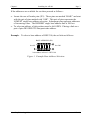
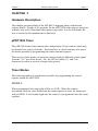
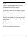
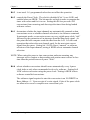
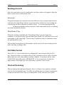
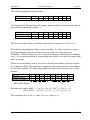
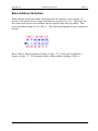
AIP-8d
Analogue Input Board
User Manual
AIP-8d
User Manual
Document Part N°
Document Reference
Document Issue Level
127-145
AIP-8d\..\127_145.DOC
1.1
Manual covers PCBs identified
AIP-8d Rev.C
All rights reserved. No part of this publication may be reproduced, stored in any retrieval system, or
transmitted, in any form or by any means, electronic, mechanical, photocopied, recorded or otherwise,
without the prior permission, in writing, from the publisher. For permission in the UK contact Blue
Chip Technology.
Information offered in this manual is correct at the time of printing. Blue Chip Technology accepts
no responsibility for any inaccuracies. This information is subject to change without notice.
All trademarks and registered names acknowledged.
Blue Chip Technology Ltd.,
The Leonard Building, Chester Aerospace Park,
Manor Lane, Deeside,
Clwyd, CH5 3QZ.
Telephone : (01244) 520222 Facsimile : (01244) 531043.
Amendment History
Issue
Level
1.0
1.1
Issue
Date
10/8/95
19/12/95
Author
Amendment Details
EGW
EGW
First approved issue, new front sheet
Addition of EMC information to Technical Section.
Errors corrected. Earlier part no. was 127-036.
Filename was ...\User_g.doc
Introduction
Page 4
Introduction
Thank you for purchasing the AIP-8d analogue input card. The card provides the
user with eight channels of 12-bit analogue inputs. The inputs range from
± 50mV to ± 5 volts, or 0 to +10 volts full scale.
The card features user selectable base address, interrupt source, interrupt level
and an on-board timer. The timer may be used as a pacer clock to control A-D
conversion cycles.
Blue Chip Technology Ltd.
127-145
About the Manual
Page 5
About the Manual
This manual is organised into four chapters, and two appendices. Each chapter
covers a different aspect of using the AIP-8d. In order to get the best results from
the product, the user is urged to read all chapters, paying particular note to
Chapter 1 which deals with the initial installation of the card. The appendices
may be used for reference at any time.
Chapter 1
Explains how to configure the card to run in your computer via the
user selectable links.
Chapter 2
Details the connections to and from the card and provides
information regarding the type of signals that card is suitable for
use with.
Chapter 3
Gives details of the card's address mapping and internal register
details allowing the user to write custom software to control the
card.
Chapter 4
Presents the card's technical specification. Use this section to
determine the card's suitability for a particular application.
Appendix A Gives a brief introduction to Binary and Hexadecimal numbering
systems for those unfamiliar with the concepts.
Appendix B Lists the IBM-PC I/O address map, interrupt and DMA allocations
and should be used along with Chapter 1 when first installing the
card.
Blue Chip Technology Ltd.
127-145
Chapter 1
Installing the AIP-8d
Page 6
CHAPTER 1
Installing the AIP-8d
Before installing the card into your computer system, there are a number of userconfigurable links that must be set.
The positioning of these links will depend upon the computer system into which
the card is being fitted. Before fitting any links to the card please read the next
section.
If you are unfamiliar with binary and hexadecimal systems a primer is included in
the appendix.
Base Address
For correct communication between the card and the host computer, the range of
addresses that the card will occupy must be set up. The base address represents
the first address that the card will use. The AIP-8d requires a total of 8 addresses
(including the base address) for correct operation. All Blue Chip Technology
boards are factory set to a default address of 300 hex. Check to ensure that the
base address and the full range of addresses are free for use.
If the addresses are not free another range must be chosen. As a guide, please use
the information contained in appendix to assist in choosing a suitable base
address.
If you are not sure refer to your computer system handbook for information
relating to other peripheral devices possibly already installed (additional
communications cards, parallel ports or games ports etc.).
Blue Chip Technology Ltd.
127-145
Chapter 1
Installing the AIP-8d
Page 7
If the addresses are available for use then proceed as follows:• Locate the row of header pins (JP1). These pins are marked “BASE” and start
with the pair of pins marked with “08H”. This pair of pins represents the
LOWEST single base address selection. Subsequent pins represent addresses
of increasing value. The HIGHEST single base address link is 200 hex.
• To select an address, a link position must be left OPEN. Placing a link on a
pair of pins DE-SELECTS that particular address.
Example: To select a base address of HEX 300, the set links as follows:BASE ADDRESS (JP1)
hex 08
hex 200
base address selected = HEX 300
Figure 1 Example Base Address Selection
Blue Chip Technology Ltd.
127-145
Chapter 1
Installing the AIP-8d
Page 8
Interrupt Selection
As part of the communication link between the AIP-8d and the host computer, an
interrupt signal may be set to occur whenever valid data is available to the user.
The use of interrupts is not essential but greatly enhances the functionality of the
card. In order for this mode of data transfer to operate correctly, the user must
select an INTERRUPT CHANNEL for the card to use. As with the selection of
base addresses, the chosen interrupt channel must be free for use. The appendix
may be used to identify the Interrupt channels that are normally already in use by
most systems and which ones will probably be free for use.
The AIP-8d allows interrupt selections from 2 to 7. Check that the Interrupt
channel free for use.
If you are not sure refer to your computer system handbook for information
relating to other peripheral devices possibly already installed (additional
communications cards, parallel ports or games ports etc.).
If the interrupt channel chosen is available for use by the AIP-8d then set up the
card as follows:• Locate the row of header pins labelled “JP2”. These pins are marked “IRQ”
and start with Interrupt Signal 2 at the set of pins marked with an arrow.
• To select an interrupt place a link on the pair of pins corresponding to the
chosen Interrupt Signal. All other pins must be left OPEN.
Example: To select an Interrupt Signal IRQ-5 set the links as follows:-
SET INTERRUPT (JP2)
2
3
4
5
6
7
INTERRUPT SELECTED = IRQ5
Figure 2 Example Interrupt Signal Selection
Blue Chip Technology Ltd.
127-145
Chapter 1
Installing the AIP-8d
Page 9
Selecting the A-D Range
The full scale measurement range for the analogue inputs is set by a combination
of user configurable links.
JP3 and JP4 set the mode of operation for the A-D. Use the table below to
determine the jumper settings for the required input scaling range.
GAIN
(JP3)
x1
x1
x1
x 10
x 10
x 10
x 100
x 100
x 100
A-D SETTING
(JP4)
+5 volts
+10 volts
± 5 volts
+5 volts
+10 volts
± 5 volts
+5 volts
+10 volts
± 5 volts
FULL SCALE
RANGE
+ 5 volts
+ 10 volts
± 5 volts
+ 500mV
+ 1 volt
± 500mV
+ 50mV
+ 100mV
± 50mV
Figure 3 Configuring the A-D
JP4
A-D SETTINGS (JP4)
JP4
JP4
+ 5 VOLTS
+ 10 VOLTS
±5 VOLTS
A-D SETTINGS (JP3)
JP3
JP3
GAIN = 1
GAIN = 10
JP3
GAIN = 100
Figure 4 Setting the Input Gain and A-D Configuration
Blue Chip Technology Ltd.
127-145
Chapter 1
Installing the AIP-8d
Page 10
Fitting the Card
Once all links have been set, the card can be installed into the host computer.
Ensure that the power is turned off and follow all of the manufacturer's
instructions for opening the computer. Locate a free expansion slot in the
machine and plug the card firmly into it. Screw the bracket in place and reassemble the computer.
NOTE: To avoid interference from other cards in the computer, if possible
locate the card away from “noisy” cards such as hard disk controllers and network
cards.
Blue Chip Technology Ltd.
127-145
Chapter 2
Making the Right Connections
Page 11
CHAPTER 2
Making the Right Connections
This chapter explains the input configuration of the AIP-8d, provides typical
connection examples and gives the pin-outs for the analogue connector.
Input Mode
The input circuitry of the AIP-8d is configurable to handle signals ranging from ±
50mV to ±5 Volts in bipolar modes and up to +10 Volts in uni-polar mode. All
modes are single ended.
A single ended input configuration measures the voltage applied to the input with
reference to the signal ground connection. This ground connection is common to
all input signals. With this input configuration the maximum voltage range that
the card can measure is +10 volts.
Input Noise
When using the 50mV full scale input, special care should be exercised in
shielding input cables against spurious noise. The A-D converter used on the
AIP-8d is extremely fast, requiring a mere 3µS to complete a 12 bit conversion.
In addition on the 50mV range, the sensitivity at the input terminals will be
approximately 12µV per bit. The card is therefore very susceptible to
interference, due to the noisy environment within the host computer and some
noise in the lower order bits will be present in the acquired signal. This noise will
be present, to a lesser degree, on all ranges and the high speed of the A-D.
Blue Chip Technology Ltd.
127-145
Chapter 2
Making the Right Connections
Page 12
Typical Connection to the AIP-8d
1
v
voltage source
single ended input
channel 1
14
25 way connector
Figure 5 Typical Connection to KFA81
Blue Chip Technology Ltd.
127-145
Chapter 2
Making the Right Connections
Page 13
Analogue Connector (25-Way D-type Plug)
This connector is located at the front of the card and protrudes through the rear
bracket. All analogue inputs are presented at this connector.
PIN
1
2
3
4
5
6
7
8
9
10
11
12
13
SIGNAL
Channel 1 Input
Channel 2 Input
Channel 3 Input
Channel 4 Input
Channel 5 Input
Channel 6 Input
Channel 7 Input
Channel 8 Input
No connection
No connection
Digital Gnd
No connection
Analogue Gnd
PIN
14
15
16
17
18
19
20
21
22
23
24
25
SIGNAL
Analogue Gnd
Analogue Gnd
Analogue Gnd
Analogue Gnd
Analogue Gnd
Analogue Gnd
Analogue Gnd
Analogue Gnd
No connection
Digital Gnd
Conversion Start/Stop
Digital Gnd
Conversion Start/Stop Signal Input:
+5 v enables the conversion process
0 v disables the conversions.
Blue Chip Technology Ltd.
127-145
Chapter 3
Hardware Description
Page 14
CHAPTER 3
Hardware Description
This chapter presents details of the AIP-8d I/O mapping along with internal
register details. Details of the registers for the µPD71054 timer chip are not given
in detail, only a brief functional description is provided. For the full details, the
user is referred to the manufacturer's data book.
µPD71054 Timer
The µPD71054 timer chip contains three independent 16-bit counters which may
be operated in a variety of modes. Presented here is a brief summary of some of
the modes possible by programming the timers internal registers.
There are five basic modes of operation each providing a different output signal
from the “Tout” pin of the device. For the AIP-8d timers 0, 1 and 2 are
connected in series to provide a longer delay period.
Timer Modes
The following modes of operation are possible by programming the control
register within the µPD71054.
MODE 0
When programmed, the output pin will be set LOW. When the counter
decrements from the value loaded into the count registers to zero, the output pin
will go HIGH. It will remain high until the count is re-programmed into the count
registers.
Blue Chip Technology Ltd.
127-145
Chapter 3
Hardware Description
Page 15
MODE 1
When the count registers are programmed, the output pin will be set HIGH.
When a LOW going signal is applied to the gate input, the count starts and the
output will immediately fall LOW. After the time period programmed into the
count registers has elapsed, the output pin will return HIGH.
MODE 2
This mode operates as a frequency divider. When programmed, the output pin is
set HIGH. When the count decrements to a value of 1 the output pin will go
LOW for ONE clock cycle only and then return HIGH. This cycle repeats
continuously reloading the same count automatically. The value can be
re-programmed and restarts the cycle.
MODE 3
This mode acts as a frequency divider with a roughly 1:1 mark-space ratio. When
programmed the output pin will toggle HIGH and LOW alternately each time the
count register decrements from the programmed value, to its base level. If the
count value programmed is an odd number then the counter will reach zero before
the output pin toggles.
MODE 4
This mode is similar to Mode 2 but the output pin pulses when the count reaches
zero instead of 1.
MODE 5
As Mode 4 except count sequence is triggered by the gate line.
Blue Chip Technology Ltd.
127-145
Chapter 3
Hardware Description
Page 16
I/O Mapping
ADDRESS
Base + 0
Base + 1
Base + 2
Base + 3
Base + 4
Base + 5
Base + 6
Base + 7
FUNCTION
Timer 0 Count Register
Timer 1 Count Register
Timer 2 Count Register
Timer Control Register
Function Control Register
A-D Start Convert
A-D Read Data
Status Register
R/W
R/W
R/W
R/W
W
W
W
R
R
Figure 6 I/O Mapping for AIP-8d
Function Control Register
This register controls various aspects of the AIP-8d operations such as input
channel selection, conversion mode etc.
Bits 4-7
BIT 7
1
1
1
1
1
1
1
1
1
1
1
1
1
1
1
1
0
BIT 6
0
0
0
0
1
1
1
1
0
0
0
0
1
1
1
1
x
BIT 5
0
0
1
1
0
0
1
1
0
0
1
1
0
0
1
1
x
BIT 4
0
1
0
1
0
1
0
1
0
1
0
1
0
1
0
1
x
SELECTS
Channel 1
Channel 2
Channel 3
Channel 4
Channel 5
Channel 6
Channel 7
Channel 8
Not Used
Not Used
Not Used
Not Used
Not Used
Not Used
Not Used
Not Used
None
x - Don’t care
Analogue Input Channel Selection Bits
Blue Chip Technology Ltd.
127-145
Chapter 3
Hardware Description
Page 17
Bit 3 is not used. It’s programmed value does not affect the operation.
Bit 2 controls the Pacer Clock. The clock is disabled if bit 3 is set LOW, and
enabled when set HIGH. The bit must be set high in order to program the
timer with values and for it to run. Setting this bit low prevents A-D
conversions from occurring and also stops the timer from being loaded
with new values.
Bit 1 determines whether the input channels are automatically scanned as data
conversions occur or whether channel selection is via software command.
In automatic mode, a conversion occurs on every eighth pacer clock “tick”
followed by the generation of an interrupt from the data ready signal. At
this point the host computer reads the data from the A-D. It is the read
operation that selects the next channel ready for the next start convert
signal from the pacer. Setting bit 1 LOW selects “manual” or software
selection of the input channel, setting it HIGH selects automatic channel
selection.
NOTE: When using the pacer to time conversions and auto scanning, any
interrupt service routine or data reading sub-routine must execute in less
time than the period between 8 pacer “ticks”.
Bit 0 selects whether conversions should occur automatically every 8 pacer
clock ticks or only when commanded to do so by software. Setting bit 0
LOW selects conversion using the pacer clock. Setting it HIGH selects
software controlled conversions.
The software signal required to start the conversion is an I/O WRITE to
Base Address +5. Upon receipt of a write signal, 8 bits of the pacer clock
are allowed to occur to complete one conversion cycle.
Blue Chip Technology Ltd.
127-145
Chapter 3
Hardware Description
Page 18
Starting A-D Conversions
A-D conversions may be started either by the pacer clock or via a software
WRITE to Base Address +5. Pacer driven conversions are straightforward
provided that any data service routine MUST be completed within 8 pacer clock
time periods. For software start conversions, it is also necessary to program the
timer. The data to the timer is loaded with bit 2 of the function control register
high. For specific details on programming the timer device for use on AIP-8d see
the next section.
Pacer Conversions
The internal logic of the AIP-8d provides one conversion result for every 8 ticks
of the pacer clock. When working out sampling rates it is important to remember
this detail and thus program the pacer clock at 8 times the desired sampling rate.
I/O Start Convert
When issuing start convert signals by I/O note that from the point of issuing the
start convert command to the point where valid data is available is 8 pacer clock
periods. The start convert signal in this mode enables a burst of pacer clocks to
drive the conversion cycle.
When using this mode therefore, the pacer clock time values should be as short as
possible to avoid unduly long times between the start convert signal and the data
ready flag.
Blue Chip Technology Ltd.
127-145
Chapter 3
Hardware Description
Page 19
Reading the A-D
Once the conversion cycle is complete the user has a choice of signals to flag that
data is ready to be read from the card.
Interrupts
Using the interrupt line represents the most efficient way to acquire data from the
card since the controlling software is not required to remain in a loop reading the
card waiting for data to become available for use. To use the interrupt facility,
an interrupt handler routine must be written and installed prior to running
the main acquisition software.
Data Ready Flag
When the A-D has valid data, the “Data Ready Flag” goes to a logic low
condition. The flag will stay low until both bytes of the A-D value have been read
whereupon it will return high. This bit may be polled in order to determine when
the data should be read.
This method of operation ties the machine up for most of the time looking for the
data ready flag to change state.
A-D Data Format
The A-D is a 12 bit resolution device although the card occupies only an 8 bit
slot. Because of this, two reads to the A-D are required to retrieve all of the data.
Both reads are to the same address (at Base Address +6) and provide the value
LOW BYTE first followed by HIGH BYTE. It is not necessary to mask the
upper nibble of the high byte since this always returns a value of zero.
Channel Scanning
When scanning through input channels, there is a limit to how quickly a channel
may be selected and then read. To allow for settling times of various components,
a scan rate not faster than 12µS is recommended. If the scan rate is too quick,
Blue Chip Technology Ltd.
127-145
Chapter 3
Hardware Description
Page 20
data values returned will not be as expected since the input will not have had time
to settle to the proper value before the A-D starts converting.
Programming the Pacer Clock
Irrespective of whether the A-D conversions are driven solely by the pacer or by
an I/O command, the µPD71054 timer must be programmed. The timer chip is
driven by a 4MHz clock signal which gives a timer resolution of 250nS. For most
timer modes, however, the minimum count period is 2 clock cycles. This means
the effective minimum time for a single counter is 500nS. For the AIP-8d, all
three timers are cascaded such that only the first timer (Timer 0) in the chain is
fed from the 4MHz clock. Timer 1 clock input signal is the output from Timer 0
and Timer 2 clock input signal is the output from Timer 1.
The minimum time period therefore for the pacer clock system as a whole is 2µS,
with the maximum being 2.23 years.
To calculate the time period for the pacer clock, work out each of the three timer
sections individually, taking the clock value for each as the output from the
preceding one.
Timer 0:
Timer 1:
Timer 2:
[CLOCK (4 MHz)/n] Hz
[CLOCK(out from Timer 0)/n] Hz
[CLOCK(out from Timer 1)/n] Hz, or
1 / [CLOCK(out from Timer 1)/n] seconds
“n” is the decimal value loaded to the counter
The pacer clock value to the A-D is the value obtained for the Timer 2
calculation. The sampling TIME for the system is 8 times the calculated time
period of the pacer.
NOTE: A pacer rate of less than 4µS is not permitted since this approaches the
conversion time for the A-D.
Blue Chip Technology Ltd.
127-145
Chapter 4
Technical Specifications
Page 21
CHAPTER 4
Technical Specifications
ANALOGUE INPUTS
Number Of Analogue Input Channels
8 (Single Ended)
Voltage Input Range
From ±50 mV to +10 Volts
or, ±5 Volts
Programmable Gains
x1, x10, x100
System Conversion Time:
A-D Conversion Time:
Resolution
Measurement Accuracy
+5V Range
+10V Range
±5V Range
Input Common Mode Range
Data Transfer Modes
Data Ready Flags
Interrupt Channels
Blue Chip Technology Ltd.
12µS min
3µS
12 bit
0.1% FS +/- 4 Counts
0.1% FS +/- 4 Counts
0.1% FS +/- 4 Counts
±12 Volts
I/O Port
Interrupt or Polling
IRQ-2 to -7
127-145
Chapter 4
Technical Specifications
Page 22
TIMERS
Number Of Timer Channels
Timer 0:
Timer 1:
Timer 2:
3
Feeds Timer 1
Feeds Timer 2
Pacer For A-D Conversions TIMER 0
(Output Feeds TIMER 1 Clock)
Timer 0 Resolution
Minimum Time Interval
Maximum Time Interval
250nS
500nS
16.384mS
Timer 1 Resolution, (Cascaded from TIMER 0)
Minimum Time Interval
Maximum Time Interval
500nS
1µS
32.768mS
Timer 2 Resolution, (Cascade From Timer 1)
Minimum Time Interval
Maximum Time Interval
1µS
2µS
65.535mS
Combined Timer Limits (Time Between Start Converts)
Minimum Time Period
Maximum Time Period
2µS
2.23 years
BOARD CONNECTIONS
Analogue Input Signals
Bus
Blue Chip Technology Ltd.
1 x 50 way male D-type
PC 8-bit ISA
127-145
Chapter 4
Technical Specifications
Page 23
Electromagnetic Compatibility (EMC)
This product meets the requirements of the European EMC Directive
(89/336/EEC) and is eligible to bear the CE mark.
It has been assessed operating in a Blue Chip Technology Icon industrial PC.
However, because the board can be installed in a variety of computers, certain
conditions have to be applied to ensure that the compatibility is maintained. It
meets the requirements for an industrial environment ( Class A product) subject to
those conditions.
• The board must be installed in a computer system which provides screening
suitable for the industrial environment.
• Any recommendations made by the computer system manufacturer/supplier
must be complied with regarding earthing and the installation of boards.
• The board must be installed with the backplate securely screwed to the chassis
of the computer to ensure good metal-to-metal (i.e. earth) contact.
• Most EMC problems are caused by the external cabling to boards. With
analogue boards particular attention must be paid to this aspect. It is
imperative that any external cabling to the board is totally screened, and that
the screen of the cable connects to the metal end bracket of the board and
hence to earth. It is recommended that round screened cables with a braided
wire screen are used in preference to those with a foil screen and drain wire.
Use metal connector shells which connect around the full circumference of the
screen; they are far superior to those which earth the screen by a simple “pigtail”. Standard ribbon cable will not be adequate unless it is contained wholly
within the cabinetry housing the industrial PC.
• If difficulty with interference is experienced the cable should also be fitted
with a ferrite clamp as close possible to the connector. The preferred type is
the Chomerics clip-on style, type H8FE-1004-AS.
• It is recommended that cables are kept as short as possible, particularly when
dealing with low level signals.
• Ensure that the screen of the external cable is bonded to a good RF earth at the
remote end of the cable.
Blue Chip Technology Ltd.
127-145
Chapter 4
Technical Specifications
Page 24
Failure to observe these recommendations may invalidate the EMC compliance.
Warning
This is a Class A product. In a domestic environment this product may
cause radio interference in which case the user may be required to take
adequate measures.
EMC Specification
A Blue Chip Technology Icon industrial PC fitted with this card meets the
following specification:
Emissions
EN 55022:1995
Radiated
Class A
Conducted
Class A & B
Immunity
EN 50082-1:1992 incorporating:
Electrostatic Discharge
Radio Frequency Susceptibility
Fast Burst Transients
Blue Chip Technology Ltd.
IEC 801-2:1984
Performance Criteria B
IEC 801-3:1984
Performance Criteria A
IEC 801-4:1988
Performance Criteria B
127-145
Appendix A
Numbering Systems
Page 25
APPENDIX A - NUMBERING SYSTEMS
Binary and Hexadecimal Numbers
The normal numbering system is termed DECIMAL because there are ten
possible digits (0 to 9) in any single column of numbers. Decimal numbers are
also referred to as numbers having a Base 10. When counting, the numbers
increment in the units column from 0 up to 9. The next increment resets the units
column to 0 and carries over 1 into the next column. This 1 indicates that there
has been a full ten (the base number) counts in the units column. The second
column is therefore termed the “tens” column.
It is more convenient when programming to use a number system that provides a
clearer picture of the hardware at an operational or register level. The two most
common number systems used are BINARY and HEXADECIMAL. These two
systems provide an alternative representation to decimal numbers.
For a binary number there are only 2 possible values (0 or 1) and as a result
binary numbering is often known as Base 2. When counting in binary numbers,
the number increments the units column from 0 to 1. At the next increment the
units column is reset to 0 and 1 is carried over to the next column. This column
indicates that a full two counts have occurred in the units column. Now the
second column is termed the “twos” column.
Hexadecimal numbers may have 16 values (0 to 9 followed by the letters A to F).
It is also known as a system with the Base 16. With this counting system the units
increment from 0 to 9 as with the decimal system, but at the next count the units
column increments from 9 to A and then B, C and so on up to F. After F the units
column resets to 0 and the next column increments from 0 to 1. This 1 indicates
that sixteen counts have occurred in the units column. The second column is
termed the “sixteens” column.
Blue Chip Technology Ltd.
127-145
Appendix A
Numbering Systems
Page 26
The following table shows how the three systems indicate successive numbers
Decimal
Base 10
0
0
0
1
0
2
0
3
0
4
0
5
0
6
0
7
0
8
0
9
1
0
1
1
1
2
1
3
1
4
1
5
1
6
1
7
1
8
1
9
2
0
0
0
0
0
0
0
0
0
0
0
0
0
0
0
0
0
1
1
1
1
1
Binary
Base 2
0 0 0
0 0 0
0 0 1
0 0 1
0 1 0
0 1 0
0 1 1
0 1 1
1 0 0
1 0 0
1 0 1
1 0 1
1 1 0
1 1 0
1 1 1
1 1 1
0 0 0
0 0 0
0 0 1
0 0 1
0 1 0
0
1
0
1
0
1
0
1
0
1
0
1
0
1
0
1
0
1
0
1
0
Hexadecimal
Base 16
0
0
0
1
0
2
0
3
0
4
0
5
0
6
0
7
0
8
0
9
0
A
0
B
0
C
0
D
0
E
0
F
1
0
1
1
1
2
1
3
1
4
Notice how the next higher column does not increment until the lesser one to its
right has overflowed.
Binary representation is ideally suited where a visual representation of a computer
register or data is needed. Each column is termed a BIT (from Binary digIT).
Only five Bits are shown in the above table. With larger numbers, more Bits are
required. Normally Bits are arranged in groups of eight termed BYTES. By
definition there are 8 BITS per BYTE. Each Bit (or column) has a value. In the
binary table above the rightmost or least significant column each digit has a value
of 1. Each digit in the next column has a value of 2, the next 4, then 8 and so on.
Blue Chip Technology Ltd.
127-145
Appendix A
Numbering Systems
Page 27
The following diagram illustrates this.
BIT No
DECIMAL VALUE
7
128
6
64
5
32
4
16
3
8
2
4
1
2
0
1
To determine the decimal value of a binary pattern, add up the decimal number of
each column containing a binary “1”.
BIT No
DECIMAL VALUE
BINARY NUMBER
7
128
1
6
64
1
5
32
0
4
16
0
3
8
0
2
4
1
1
2
1
0
1
0
The above example shows the binary pattern that is equivalent to 198 Decimal.
The binary string defining a Byte can be unwieldy. To make it less error prone,
the 8 bits forming a byte are divided into two groups of 4 bits, known as
NIBBLES. With four bits there are 16 possible numeric combinations (including
zero). A convenient method of representing each nibble is to use the hexadecimal
base 16 system.
When converting binary to hex, the byte is divided into nibbles each represented
by a single hex digit. This technique is applied to the selection of the base address
for the circuit board. The following diagram illustrates the construction of a hex
number.
BIT No
NIBBLE VALUE
BINARY NUMBER
HEXADECIMAL:
7
8
1
6
4
1
5
2
0
4
1
0
º¶¶¶¶¶¾¶¶¶¶¶¶»
3
8
0
2
4
1
1
2
1
0
1
0
º¶¶¶¶¶¶¾¶¶¶¶¶¶»
C
6
Hexadecimal upper nibble = (1 x 8) + (1 x 4) + (0 x 2) + (0 x 1) = 12
lower nibble = (0 x 8) + (1 x 4) + (1 x 2) + (0 x 1) = 6
The resulting value is C6 Hex, since 12 Decimal equals C Hex.
Blue Chip Technology Ltd.
127-145
Appendix A
Numbering Systems
Page 28
Base Address Selection
Each column can be physically represented on the board by a pair of pins. In
practice, the boards cover a range of addresses (usually 16 Decimal). Therefore the
low order four bits are not included, but two higher order bits are added. This
gives an address range of 0 to 3F0 Hex . The following diagram shows a typical set
of pins.
Here a link is fitted to denote a binary or logic “0”, or left open to indicate a
binary or logic “1”. The example shows a base address setting of 300 Hex.
Blue Chip Technology Ltd.
127-145
Appendix B
PC Maps
Page 29
APPENDIX B - PC MAPS
PC/XT/AT I/O Address Map
Address
Allocated to:
000-01F
020-03F
040-05F
060-06F
070-07F
080-09F
0A0-0BF
0F0
0F1
0F8-0FF
1F0-1F8
200-207
278-27F
2F8-2FF
300-31F
360-36F
378-37F
380-38F
3A0-3AF
3B0-3BF
3C0-3CF
3D0-3DF
3F0-3F7
3F8-3FF
DMA Controller 1 (8237A-5)
Interrupt Controller 1 (8259A)
Timer (µPD71054)
Keyboard Controller (8742) Control Port B
RTC and CMOS RAM, NMI Mask (Write)
DMA Page Register (Memory Mapper)
Interrupt Controller 2 (8259)
Clear NPX (80287) Busy
Reset NPX (80287)
Numeric Processor Extension (80287)
Hard Disk Drive Controller
Reserved
Reserved for Parallel Printer Port 2
Reserved for Serial Port 2
Reserved
Reserved
Parallel Printer Port 1
Reserved for SDLC Communications, Bisync 2
Reserved for Bisync 1
Reserved
Reserved
Display Controller
Diskette Drive Controller
Serial Port 1
Blue Chip Technology Ltd.
127-145
Appendix B
PC Maps
Page 30
PC/XT Interrupt Map
Number
Allocated to:
NMI
0
1
2
3
Parity
Timer
Keyboard
Reserved
Asynchronous Communications (Secondary)
SDLC Communications
Asynchronous Communications (Primary)
SDLC Communications
Fixed Disk
Diskette
Parallel Printer
4
5
6
7
Blue Chip Technology Ltd.
127-145
Appendix B
PC Maps
Page 31
PC/AT Interrupt Map
Level
Allocated to:
CPU NMI
CTLR 1
Parity or I/O Channel Check
CTLR 2
IRQ 0
IRQ 1
IRQ 2
IRQ 8
IRQ 9
IRQ 10
IRQ 11
IRQ 12
IRQ 13
IRQ 14
IRQ 15
IRQ 3
IRQ 4
IRQ 5
IRQ 6
IRQ 7
(Interrupt Controllers)
Timer Output 0
Keyboard (Output Buffer Full)
Interrupt from CTLR 2
Real-time Clock Interrupt
S/w Redirected to INT 0AH (IRQ 2)
Reserved
Reserved
Reserved
Co-processor
Fixed Disk Controller
Reserved
Serial Port 2
Serial Port 1
Parallel Port 2
Diskette Controller
Parallel Port 1
DMA Channels
0
1
2
3
Memory Refresh
Spare
Floppy Disk Drive
Spare
Blue Chip Technology Ltd.
127-145