1
DA600User'sManual
ffi
RealTimeDevices,
Inc.
"AccessingtheAnalog World",*
ISO9001 and AS9100 Certified
DA6OO
UsertsManual
ffi
REALTIMEDEVICES,
INC.
820NorthUniversity
Drive
PostOfficeBox906
StateCollege,
Pennsylvania
16804
Phone:(814)234-8087
FAX:(B1a)
234-5218
Publishedby
RealTimeDevices,Inc.
820N. UniversityDr.
P.O.Box 906
StateCollege,PA 16804
CopyrightO 1991by RealTimeDevices,Inc.
All righS reserved
Prinredin u.S.A.
Rev.A 9211
TABLE OF CONTENTS
rNTRODUCTrON......
.............t-1
WhatComes
CHAPTER 1 - BOARD SETTINGS
Factor-Config
(FacorySetting:
P2- BaseAddress
3@hex(768decimal).................
Polarity(Factory
P3- AnalogOutputChannel
Sening:All Channels
Unipolar)
CHAPTER 2 - BOARD INSTALLATION
ConnectingtheAnalogOuputPins
CHAPTER3 _ HARDWAREDESCRIPTION
..........
CHAPTER 4 - BOARD OPERATION AND PROGRAMNdING
BA + 0: Channel
(WriteOnly)...........
I (AOUTI)LSBInputRegister
BA + 1: Channel
t (AOI-ff1)MSBInputRegister
(WrireOnly)...........
(AOUT2)LSBInputRegister
BA + 2: Channel2
(WrireOnly)...........
BA + 3: Channel
2 (AO|.dfZ)
(WrireOnly)...........
MSBInpurRegisrer
BA+ 8: Update
AOLnI andAOUT2(WriteOnly)...........
BA + 16:ClearAOUTIandAOUT2(WriteOnly)...........
BA+ 24: Channel
(WrireOnly)...........
3 (AOUT3)LSBInputRegisrer
(AOUT3)
+
BA 25: Channel
(WrireOnly)...........
MSBInputRegister
3
(AOUT4)
BA+26: Channel4
(WrireOnly)...........
LSBInputRegisrer
(AOUT4)MSBInputRegister
BA+ 27: Channel4
(WrireOnly)...........
BA + 32:Update
AOUT3andAOUT4(WriteOnly)...........
BA + 40:ClearAOUT3andAOUT4(WriteOnly)...........
l,exiconTestandDiagnostics
Tool............
D/A Conversion
Flow
CHAPTER5 - CALIBRATION
Unipolar
1-l
..............1-3
......................
1-4
2-l
..........24
..............3.1
.4-t
.................4-3
................44
.................44
................44
................44
.................44
...............44
..............44
...............4-s
..............4,5
..............4-5
.................4-s
........,......4-7
5-l
APPENDIX A _ DA6OOSPECIFICATIONS
APPENDIXB - CONNECTORPIN ASSIGNMENTS
APPENDIXC-WARRANTY
.........A.1
-...........C-1
LIST OF ILLUSTRATIONS
1-1
t-2
r-3
2-l
2-2
3-1
4-l
4-6
5-1
Settings........
BoardLayoutShowingFactory-Configured
n ..,..,..........
BaseAddress
Jumper,
P3 ................
AnalogOutputChannelPolarityJumpers,
Assignments
P4llO ConnectorPin
AnalogOutputConnections
DA600BlockDiagram
D/A ConversionFlow Diagram
ContinuousConvertModeFlow Diagram
Trimpots......
BoardLayoutShowingCalibration
........1-3
......................14
...........14
......................2-3
.............24
....................3-3
.......4-8
............4-7
......................5-3
INTRODUCTION
The DA600 duaVquadchannelanalogoutputboardurrnsyour IBM PC/XT/AT or compatiblecomputerinto a
high-performancetestingand control system.Installedwithin a singleshortor full-size expansionslot in the
computer,the DA600 features:
2 or 4 analogoutputchannels,
. 12-bitresolution,
. Simultaneous
updatingof eachpair of ouput channels,
. 5 or l0 volt, unipolar or bipolar outputs.
The following pamgraphsbriefly describethe major functionsof the board.More detaileddiscussionsof board
functionsareincludedin Chapter3,HardwareDesciption, andChapter4,Board OperationandProgramming.The
boardsetupis describedin Chapterl, Board Settings.
Di gital-to-AnalogConversion
The digital-to-analog(D/A) circuitry featurestwo 12-bitconverterchannelsin each AD7537D/A converterIC.
Your boardprovidestwo or four ouput channels,dependingon the numberof channelsspecifiedwhen ordering.
The two channelsin eachAD7537 areintemally doublebufferedandcan be simultaneouslyupdated.The ouput
voltagerangeis controlledby precisionvoltagereference(s)installedon the boardat U6 for AOUTI and AOUT2
and UlO for AOUT3 andAOUT4. A 5 volt or a l0 volt referenceis specifiedwhen ordering.The 5 volt reference
provides0 to +5 and-5 to +5 volt outputranges,andthe 10volt referenceprovides0 to +10 and-10 to +10 volt
outputranges.Eachchannelisjumper selectablefor unipolaror bipolar operation.
What ComesWith Your Board
You receivethe following itemsin your DA600 package:
. DA600 interfaceboard(numberof channelsandreferencevoltageuserspecified)
. Softwareand diagnosticsdiskettewith exampleprogramsin BASIC, Turbo Pascal,andTurbo C; sourcecode
. IJser'smanual
pleasecall RealTime Devices'CustomerServiceDepartrnent
If any item is missingor damaged,
at
(814)234-8087.If you requireserviceoutsidetheU.S.,contactyour local disributor.
In additionto the items includedin your DA600 package,Real Time Devicesoffers a full line of boardirccessories. Key accessories
for ttreDA600 include the TB40 terminalboardand XB40 prototlpe/terminalboardfor
prototypedevelopmentandeasysignalaccess,EX-XT andEX-AT extenderboardsfor simplified testingand
debuggingof prototypecircuitry, andXC40 singlewire flat ribbon cableassembliesfor externalinterfacing.
UsingThis Manual
Thismanual
is intended
tohelpyouinstallyournewboardandgetit running
quickly,whilealsoproviding
enoughdetail aboutthe boardandis functionsso that you canenjoy maximumuseof its featuresevenin the most
complexapplications.We assumethat you alreadyhavean understandingof daa acquisitionand connol principles
and that you can customizethe examplesoftwareor write your own applicationsprogmms.
When You NeedHelp
This manualand theexampleprogramsin the softwarepackageincludedwith your boardprovide enough
information to properly useall of theboard'sfeatures.If you haveany problemsinstalling or using this board,
contactour TechnicalSupportDepartment,(814) 234-8087,during regularbusinesshours,easlsrnstandardtime or
e;sterndaylight [ime, or senda FAX requestingassistanceto (814) 234-5218.When sendinga FAX request,please
includeyour company'snameandaddress,your name,your telephonenumber,and a brief descriptionof the
problem.
i-3
CHAPTER1
BOARDSETTINGS
The DA600 boardhasjumper settingsyou canchangeif
necessaryfor your application.The boardis factory-configured
with the mostoftenusedsettings.The factorysettingsarelisted
and shownon a diagramin thebeginningof this chapter.Should
you needto changethesesettings,usetheseeasy-to-followinstructionsbeforeyou install the boardin your computer.
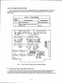
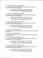
Factory-ConfiguredJumper Settings
jumperson the DA600 board.Figure l-l showsthe
Table l-l lists the factory settingsof the user-configurable
boardlayout and the locationsof the factory-setjumpers.The following paragraphsexplain how to changethe
factarysettings.
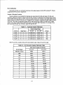
Table1-l - FactorySettlngs
Switch/
Jumper
FunctlonControlled
FactorySettlng
P2
Setsthe baseaddress
300 hex(768decimal)
P3
Selectsa unipolaror bipolaroutputfor each
analogchannel
Unipolar
ilfin*nmilFHHH
ftiilil?FHH
I REFo( | oPor(I
Ap?$?
? tAp#(
| Apilrl
;frfril,#""$-il$ft:0JJ,ffi1
*ls
P1
IREFt l-op.,?I
u1o':;ryJ"
;[ l*,,,
u,5
Api$tfff'R
:i lSSl
l-Al-'
.,.tl#l
",'0
il_F-'
"$tl.fffir,
t=ffugu&=t?fr,ro*,ouad
I ;[ 1,."," r
DAC
*-o"Hmgm
r[ f.,,* f u[1,.,-,'-t[J1,."* f ru
fr*!'amff:'n"*U,
ur
u2
u3
11u",
*
..jll@-3mr
Fig. 1-1 -
F
A1-
Board LayoutShowingFactory-Configured
Settings
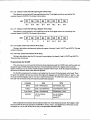
P2 - BaseAddress(Factory Seffing:300 hex (768decimal))
Oneof themostcommoncausesof failurewhenyou arefirst trying your boardis addresscontention.Someof
your computer'sI/O spaceis alreadyoccupiedby internalVO and otherperipherals.When the DA600 board
attemptsto useI/O addresslocationsalreadyusedby anotherdevice,contentionresultsand ttreboarddoesnot work.
l-3
To avoid this problem,the DA600 hasa headerconnector,P2, which lets you selectany one of eight sarting
in the computer'sVO. Shouldthe factory settingof 300 hex (768 decimal)be unsuitablefor your system,
addresses
you can selecta different baseaddress.Theseaddresses
are,from left o right on P2:
Hexadeclmal
Declmal
20a
s12
240
576
280
640
2C0
704
300
768
340
832
380
896
3C0
960
To changethe baseaddresssetting,removethejumper from the fifth from left pair of pins (300 hex) and,using
Figure 1-2 asa guide, install it in the desiredlocation.Recordthe new baseaddresssettingon ttre table inside the
back coverof this manual.
8s8E8S8E
N6|A|G|(|iIc:Ic'G'
xxxxxxxx
P2
o ooo?ooo
I
a oooooao
Fig. 1-2 -
Base AddressJumper,P2
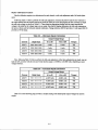
P3 - Analog Output ChannelPolarity (Factory Setting:Atl ChannelsUnipolar)
HeaderconnectorP3, locatednext to [O connectorP4, lets you individually seteachchannelfor unipolaror
bipolar operation.When setfor unipolar,the output is 0 to +5 or 0 to +10 volts, dependingon the precisionvoltage
referenceinsalled on theboard.Whensetfor bipolar,theouput is -5 to +5 or -10 to +10 volts.Figure l-3 shows
this headerconnector.Note that ttreboardis factory-calibratedfor unipolar.When you changethe polarity, you
shouldcalibratethe boardasdescribedin Chapter5.
P3
+l]-
+
+
]*
+l+l-
tct
+
+
+l-
H
J
-J
lq
o
Fig.1-3- AnalogOutputChannelPolarity
Jumpers,
P3
t-4
CHAPTER2
BOARD INSTALLATION
TheDA600 boardis easyto installin your IBM PCIXT/AT or
compatiblecomputer.It canbeplacedin any slot, shofior fullsize.This chaptertells you step-by-step
how to install andconnect
the board.
2-l
Board Installation
Keep the boardin its antistaticbag until you arereadyto install it in your computer.Whenremoving it from the
or conneclors.
bag,hold theboardat theedgesanddo not touchthecomponents
Beforeinstallingtheboardin your computer,checkthejumperseffings.Chapter1 reviewsttrefactorysettings
and how to changethem.If you needto changeany settings,refer to the appropriateinstructionsin Chapter1. Note
that incompatiblejumper settingscanresult in unpredictableboardoperationanderratic response.
To install the board:
1. Turn OFF the powerto yoru computer.
2. Removethe top coverof thecomputerhousing(referto yourowner'smanualif you do not alreadyknow
how to do this).
3. Selectany unusedshortor full-sizeexpansionslotandremovethe slot bracket.
4. Touchthemetalhousingof thecomputerto dischargeany sulticbuildupandthenremovetfteboardfrom its
antistaticbag.
5. Holdingtheboardby its edges,orientit so thatits cardedge(bus)connectorlinesup with the expansionslot
connectorin thebottomof theselectedexpansionslot.
6. After carefully positioningthe board in the expansionslot so that the card edgeconnectoris restingon the
computer'sbusconnector,gentlyandevenlypressdownon theboarduntil it is securedin the slot
NOTE: Do not force the boardinto the slot. If theboarddoesnot slide into place,removeit and try again.
Wiggling the boardor exertingtoo muchpressurecan result in damageto the boardor to the computer.
7. Afterthe boardis installed,securetheslot bracketbackinto placeandput thecoverbackon your computer.
The boardis now readyn be connectedvia the externalI/O connectorat therear panelof your computer.
External VO Connections
Figure2-I showstheDA600'sP4 VO connectorpinout.Referto thisdiagramasyou makeyour VO connections.
Ai{ALOG GI{D
AOUTI
AOUT2
AOUT:I
AOUT4
t{.c.
ANALOG GND
N.C.
l{.c.
N.C.
N.C.
AIIALOG GNO
a{.c.
N.C.
l{.c.
N.C.
t{.c.
N.C.
N.C.
il.c.
lt.c.
N.C.
N.C.
N.C.
N.C.
N.C.
N.C.
lt.c,
t{.c.
N.C.
lt.c.
N.C.
t{.c.
'|C.
ll.c.
N.C.
+12 VOLIg
NESET ORY
.12 VOTTS
DIGITAL GNO
Fig.2-1- P4 VOConnector
PinAssignments
2-3
Connectingthe Analog Output Pins
The analogoutputsareconnectedto their loadsas shownin Figure2-2.The high sideof thedevicereceiving
theoutputsignalis connected0otheappropriat€AOUT channeland thelow sideis connectedto oneof tle three
ANALOG GND pins (P4-1,P4-7,orP4-12).
OP.AMP
BUFFERS
600
I/O CONNECTOR
P4
LOAD
A N A L O GG N D
Fig.2-2- AnalogOutputConnections
.A
CHAPTER3
HARDWAREDESCRIPTION
This chapterdescribes
theDA600 D/A circuitry.EachD/A
outputchannelcircuit hastwo mainelements:theD/A converter
and the output amplifier.
3-1
The DA600 boardfeaturestwo or four analogoulput channelswhich canbe usedfor PC generationof analog
signalsfor industrial control and testingapplications.The following paragraphsdescribettte D/A circuitry.
Fig.3-1- DA600
BlockDiagram
D/A ConversionCircuitry
The DA600 boardperformsdigital-to-analogconversionson up to four analogoutput channels.The following
paragraphsdescribethe D/A circuiry.
D/A Converter
The AD7537 l2-bit D/A convertercontainstwo closely matched,monotonicD/A converterchannelsin a single
IC packageto provide excellentthermalracking acrosseachpair of analogoutputs.The datato be convertedis
doublebufferedat the D/A input, which allows simultaneousupdatingof both D/A outputchannels.The D/A
converterregisterscan be clearedasynchronouslyundersoftwarecontrol.
The AD7537is a multiplying D/A converterwhich convertsa digital input into a curent output. The conversion
is performedby a highly stableR-2R ladderand 12currentsteeringswitches.
Output Amplifiers
The AD712precisionoperationalamplifierconvertstheAD7537'scurrentoutputto a unipolaror bipolar
voltage.EachAD712packagecontainstwo high speedmonolithicop amps,onefor eachoutputfrom theAD7537
D/A converterpackage.The exceptionallylow offset voltageanddrift ensurean accurateanalogouput on each
channel.
J-J
Output Range
The D/A channel'soutputrangeis determinedby the precisionvoltagereferenceinstalledon the DA600 board
(you canorder the boardwittt a 5- or l0-volt refererrce),andby the settingof thejumperson P3. Channelscanbe
independentlysetfor unipolar or bipolar operation.
3-4
CHAPTER4
BOARD OPERATION AND PROGRAMMING
This chapterdesqibesthe DA600 operationandprovidesa
completedescriptionof the AO mapanda flow diagramto aid you
in programmingyour DA600 board.The exampleprogramsincludedon the disk in your boardpackagearedescribedat the end
of this chapter.Theseprograms,writtenin BASIC, TurboPascal,
andTurboC, includesourcecodeto simplify your applications
programming.
4-l
Definingthe VO Map
The VO map for the DA600 is shownin Table4-1. The baseaddress(designafedasBA) canbe selectedby
settingthejumper on P2, as describedin Chapterl, Board Seuings.One of eight sarting addresslocationscanbe
selected.The board is shippedwith the baseaddresssetat 3m hex (768 decimal).The following sectionsdescribe
the registercontentsof eachaddressusedin the VO map.
Table 4-1 - DA600l/O lr/hp
ReadFunctlon
RegisterDescrlptlon
Channell(AOUT1)
LSB
Not used
InputRegister
MSB
Channell(AOUT1)
Not used
lnputRegister
Wrlte Functlon
Programs
AOUTI LSB,
bits 0-7
LSB
Channel2(AOUT2)
InpulRegister
MSB
Channel2(AOUT2)
InputRegister
Programs
AOUT2LSB,
bits0-7
Programs
AOUT2MSB,
bits8-'11
Nol used
Notused
Update
AOUT1/AOUT2
Notused
Clear
AOUTI/AOUT2
Notused
Programs
AOUT1MSB,
bits8-11
Simultaneously
updates
AOUT1& AOUT2
ClearsAOUTI& AOUT2
registers
Address'
(Declmal)
BA+0
B A +1
BA+2
BA+3
B A +8
B A +1 6
(AOUT3)
LSB
ChannelS
lnpulRegister
Not used
Channels(AOUT3)
MSB
InputRegister
Notused
Channel4(AOUT4)
LSB
lnputRegister
Notused
Programs
AOUT3LSB,
bits0-7
Programs
AOUTSMSB,
bits8-11
Programs
AOUT4LSB,
bits0-7
MSB
Channel4(AOUT4)
InputRegister
Notused
Programs
AOUT4MSB,
bits8-11
BA+27
AOUTS/AOUT4
Updare
Notused
Simultaneously
updates
AOUT3& AOUT4
BA+32
Not used
ClearsAOUT3& AOUT4
registers
BA+40
AOUTS/AOUT4
Clear
' BA = BaseAddress
BA+24
BA+25
BA+26
BA + 0: Channell (AOUTI) LSB Input Register(Write Only)
This addressis usedto load the 8 leastsignificantbits of the 12-bit digital word to be convertedby D/A
converterchannel1 (AOUTl). The formatis shownbelow.
LSB
D7
D6
D5
D4
D3
D2
D1
DO
Bit7
Bir6
Bir5
Bir4
Bit 3
Bit 2
Bir1
Bir0
4-3
BA + 1: Channel I (AOUTI) MSB Input Register(I{rite Only)
This addressis usedto load the 4 most significantbits of ttre 12-bit digital word to be convertedby D/A
converterchannel1 (AOUTD. Theformatis shownbelow.
MSB
D7
D6
D5
D4
D3
D2
D1
DO
x
Bit11
Bit10
Bit 9
BirI
BA + 2: Channel2 (AOUT2) LSB Input Register(Write Only)
This addressis usedo load the 8 leastsignificantbits of the l2-bit digital word to be convertedby D/A
converterchannel2(AOUT2).The formatis shownbelow.
LSB
D7
D6
D5
D4
D3
D2
D1
DO
BitT
Bit6
Birs
Bit4
Bit3
Bit2
Bitl
Bit0
BA + 3: Channel2 (AOUT2) MSB Input Register(Write Only)
This addressis usedto load ttre4 most significantbits of dp 12-bit digital word to be convertedby D/A
converterchannel2 (AOUT2). The format is shownbelow.
MSB
D7
D6
D5
D4
D3
D2
D1
DO
Bit11
Bit10
Bit9
BitI
BA + 8: UpdateAOUT1 and AOUT2 (Write Only)
Writing to this addresssimultaneouslyupdatesthe outputsof channels1,and2 (AOUTI and AOUT2). The data
written is irrelevant.
BA + 16: Clear AOUT1 and AOUT2 (Write Only)
Writing to this addressclearsthe D/A converter'sinput registersfor channelsI and2 (AOUTI and AOUT2).
The datawritten is irrelevanl
BL + 24: Channel3 (AOUT3) LSB Input Register(IMrite Only)
This addressis usedo load ttre 8 leastsignificantbits of the 12-bit digital word to be convertedby D/A
converterchannel3 (AOUT3). The format is shownbelow.
LSB
D7
D6
D5
D4
D3
D2
D1
DO
BitT
Bit6
Birs
Bh4
Bit3
Bit2
Bitl
Bit0
BA + 25: Channel3 (AOUT3) MSB Input Register(Write Only)
This addressis usedto load the 4 most significantbits of the l2-bit digital word to be converredby D/A
converterchannel3 (AOUT3).Theformatis shownbelow.
MSB
D7
D6
X
X
D5
D3
D2
D1
DO
Bir11
Bit10
Bit9
Bit8
D4
4-4
BA + 26: Channel4 (AOUT4) LSB Input Register(Write Only)
This addressis usedo load the 8 leastsignificantbits of the 12-bit digital wud to be convertedby D/A
converterchannel4(AOUT4).The formatis shownbelow.
LSB
D7
D6
D5
D4
D3
D2
D1
DO
BitT
Bit6
Birs
Bh4
Bit 3
Bir2
Bit 1
Bit 0
BA + 272 Channel4 (AOUT4) MSB Input Register(Write Only)
This addressis usedto load the 4 most significantbits of the 12-bit digital word to be convertedby D/A
converterchannel4 (AOUT4). The format is shownbelow.
MSB
D7
D6
D5
D4
D3
D2
D1
DO
Bit11
Bir10
BirI
BitI
BA + 32: UpdateAOUT3 and AOUT4 (Write Only)
Writing to ttris addresssimultaneouslyupdatesthe outputsof channels3 and4 (AOUT3 and AOUT4). The data
written is irelevanL
BA + 40: Clear AOUT3 and AOUT4 (Write OnIy)
Writing to this addressclearsthe D/A converter'sinput registersfor channels3 and 4 (AOUT3 and AOUT4).
The datawritten is irrelevant.
Programmingthe DA600
This sectiongives you somegeneralinformationaboutprogtammingand the DA600 board,and thenwalks you
throughthe major DA600 programmingfunctions.Thesedescriptionsand the flow diagramat the end of this
chapterwill help you as you usethe exampleprogmmsincludedwith the board.All of the programdescriptionsin
this sectionusedecimalvaluesunlessothenvisespecified.
The DA600 is programmedby writing to andreadingfrom the correctVO port locationson the board.These
VO pors weredefinedin the previoussection.Most high-levellanguagessuchasBASIC, Pascal,C, and C++, and
of courseassemblylanguage,makeit very easyto read/rvritetheseports. The able below showsyou how to read
from and write to VO ports using somepopularprogramminglanguages.
Language
BASIC
TurboC
Turbo Pascal
Assembly
Bead
Data= INP(Address)
Wrlte
OUTAddress,Data
Data= inportb(Address) outportb(Address,
Data)
Data:= Port[Address]
Pod[Address]
:= Data
movdx, Address
in al,dx
movdx, Address
moval, Dala
outdx,al
Manycompilershavefunctionsthatcanread/writeeitherEor 16bits ftom/toanVOport.Forexample,
Turbo
PascalusesPort for 8-bitportoperations
andPortW for 16bits,TurboC usesinportb for an8-bitreadof a port
andinportfor a 16-bitread.Besureto useonly 8-bitoperations
with theDA600!
4-5
D/A Conversions
D/A conversionsareperformedon eachpair of channels,AOUTI/AOUT2 or AOUT3/AOUT4, by writing data
to the D/A converterregistersand thenissuingan updatecommandwhich simultaneouslyupdatesthe ouputs of
both channels.The D/A converterregistersalsocanbe simultaneouslyclearedby issuinga clear command.
It is goodpracticeto start your programby clearingthe D/A converterregisters.If your boardhastrvo output
channels,AOUT1 and AOUT2, ttris is a singlestepprocessaccomptshedby writing to BA + 16.The datawriren is
furelevant.If your boardhasfour outputchannels,AOUTI throughAOUT4, you write to BA + 16 and BA + 40 to
clearall regisfers.
After clearingthe registers,you load the l2-bit digital datafor eachchannelin a two stepprocess,LSB followed by MSB. After the datahasbeenloadedfor eachpair of channels,the channelsare simultaneouslyupdatedby
issuingthe updatecommand.The digital datais converted!o a correspondingvoltagewhich is presentat the ouput
until anotherupdatecommandis issued,changingthe value,or the clearcommandis issued.The flow diagramat
the end of this chaptershowsthesesteps.
The outputvoltagerangesare determinedby the voltagereferenceinstalledon the board and the settingsof the
unipolar/bipolarchanneljumperson P3. Onereferenceis installedfor eachpair of output channels(U6 for AOLrf l/
AOUT2 and U10 for AOUT3/AOUT4). VoltagerefererrceREF-02provides5 volts andREF-01provides 10 volts.
Unipolar or bipolar operationcanbe individually seton a per channelbasison P3. The tablesbelow showkey
digital inputsand their conespondingoutputsfor unipolarandbipola,rranges.The resolutionfor eachrangein
includedin therangecolumnheading.
Table
UnlpolarD/AConverslon
Digitallnput
0 b +5VoltOutput
0 b +10VoltOulput
(Resolu$on:122
mV) (Resolutlon:2.44
mV)
MSB000000000000LSB
0 volls
0 volts
100000000000
volls
+2.5000
volls
+5.0000
11111 1 1 1111
+4.9988
volts
volts
+9.9976
BipolarD/AConverslon
Table
Digitallnput
-5to +5VoltOuFut -10to +10VoltOutput
(Resolution:2.44
mV)
mV) (Resoluton:4.88
MSB000000000000LSB
volls
+5.0000
+10.0000
volts
100000000000
0 vdts
0 tolls
111111111111
-4.9976
vols
-9.9951
vofis
4-6
ExamplePrograms
The softwareincludedwittr your DA600 boardcontainsexampleprogfims in BASIC, Turbo Pascal,and Turbo
C to help you get startedusing the board.Theseprogrms showyou how to setthe outputsand how to generate
rampfunctions.Sourcecodeis alsoincluded.
The DA600 boardis easilyprogrammedfrom any high-levellanguage'sVO referenceinstructions.In BASIC,
tlreseinstructionsareINP and OUT; in Turbo Pascal,they areport and port; and in Turbo C, they are inportb and
oulportb.
Beforeusing the softwareincludedwith your board,makea backupcopy of the disk. You may makezrsmany
backupsasyou need.
Lexicon Test and DiagnosticsTool
An interactivedatacollection andplotting utility program,IJxicon, is providedasa test and diagnosticstool.
program
The
is self-explanatoryusing ttreinstructionson disk.
4-7
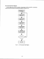
D/A ConversionFlow Diagram
This flow diagramshowsyou how to generatea voltageoutputon AOUT1 and AOUT2. A conversionis
initiated eachtime the channelsare simultaneouslyuSated by writing to BA + 8.
LoadAOUT1
MSB
(D8-Dl1)
Register
LoadAOUT2MSB
(D8-Dl1)
Register
Fig.4-1- D/AConversion
FlowDiagram
4-8
CHAPTER5
CALIBRATION
This chaptertells you how to calibratetheDA600 analog
oulputsusingtheeight trimpotson the board.Theserimpots
calibratethe D/A for unipolaror bipolar operation.Calibration
may be requiredif you changethe voltagerangeor polarity of a
channel,or wheneveryou suspectinaccuratereadings.
5-l
This chaptertells you how to calibratethe D/A converterfor unipolar or bipolar operation.The boardhasbeen
factory-calibratedfor unipolaroperation.Unipolar calibrationis accomplishedby making a full-scale adjusunenton
eachoutput channel.Bipolar calibrationinvolves makinga mid-scaleand full-scaleadjustmenton eachchannel.
Any time you suspectinaccuratereadings,you can checkthe accuacy of your conversionsusing the procedure
as necessary.
below,andmakeadjustments
Calibrationis donewith theboardinstalledin your PC. You canaccessthe trimpots with the computer'scover
removed.Powerup the computerand let the boardcircuitry stabilizefor 15 minutesbefme you startcalibnating.
RequiredEquipment
The following equipmentis requiredfor calibration:
. Digital Voltmeter:5-12 digits
. Small Screwdriver(for trimpot adjustment)
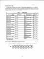
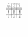
Figure 5-1 showsthe boardlayout.The eight trimpotsusedfor calibrationare shadedin the upperright areaof
the board.Trimpots 1 through4 areusedwhen adjustingAOUTI and AOUIZ, and trimpots 5 through8 are used
when adjustingAOUT3 and AOUT4. If your boardhasonly two outputchannels,ignore ttreadjustmentsfor
AOUT3 andAOUT4.
R1
I
iililffiffiffiffiil
no_nmilFffiffiffi
';ft *'$-ilH'ft:0-ilJ-ffi
,,
fiil,#
rL,
(
I REFor
I oecil l-
Ap?$i? lip
Fo.ii?
P4
I REdt I oPorll-
Ap?$?
1 lAo?r4 lAo?'rl
':;.
Fig.5-1- BoardLayoutShowingCalibration
Trimpots
5-3
D/A Calibration
During this procedure,you will makeconnectionsto the analogoutputsat externalVO connectorP4. The pin
assignmentsfor P4 aregiven in AppendixB.
Unipolar Calibration Frocedure
Unipolar calibrationis accomplishedby adjustingeachoutputchannelfor full-scaleoutput. The full-scale
adjustmentcalibratesthe referencevoltageusedby ttreD/A converter!o compensatofor the analogouput circuiry
of the DA600. Following Table 5-1 below, connectttrepositive leadof your voltmeter!o the outputchanneland the
negativeleadto an ANALOG GND pin on P4. Programthe D/A converterto output the full-scale voltage,as shown
in the table.Then adjustthe appropriaterimpot until the outputmatchesthe voltagein the table fu the voltage
rangeyou are using.VoltagereferenceREF-02providesa 5-volt range;REF-01providesa lO-volt range.If you
havea two-channelboard,you will needlo adjustTRI andTR2 only.
Table5-1- Full-ScaleUnlpolarCallbratlon
OutputVoltageRange
Channel
Dlgitallnput
0 to +5V
0 to +10V
Trlmpot
AOUTl
1 1 1 11 1 1 11 1 ' t 1
+4.9988volts
+9.9976volts
TR1
AOUT2
+4.9988vohs
+9.9976vohs
TR2
AOUT3
1 1 1 11 1 1 11 1 1 1
1 1 1 1' 1 1 1 11 1 ' t 1
+4.9988vohs
+9.9976 volts
TR5
AOUT4
1 1 1 11 1 1 11 1 1 1
+4.9988volts
+9.9976volts
TR6
Table 5-2 providesa completelisting of the ideal unipolarouput voltagesfor eachbit weight.
Table5-2- D/A ConverterUnipolarCalibrationTable
ldealOutputVoltage(in millivolts)
D/ABitWelght
0to+5V
0to+10V
4095(Max.Output)
4998.8
9997.6
2048
2500.0
5000.0
1024
1250.0
2500.0
512
625.00
1250.0
2s6
312.50
625.00
128
156.250
312.50
64
78.12s
156.2s0
32
39.063
78.125
16
19.s313
39.063
8
9.7656
19.s313
4
4.8828
9.7656
2
2.4414
4.8828
1
1.2207
2.M14
0
0.0000
0.0000
5-4
Bipolar Calibration Procedure
Bipolar calibrationrequirestwo adjustmentsfor eachchannet a mid-scaleadjustmentand a full-scale adjustmenL
Following Table 5-3 below, perform the mid-scaleadjustment.Connectthe positive leadof your voluneterto
the output channeland the negativelead to an ANALOG GND pin on P4 and programthe D/A converterto output
the mid-scalevoltage,asshownin Table 5-3. Thenadjustthe appropriaterimpot until the oulput matchesthe
voltagein the table for the voltagerangeyou are using.Note that fc bipolar calibration,the mid-scaletrimpotsare
the sameas thoseusedfor full-scale unipolarcalibration.VoltagereferenceREF42 providesa 5-volt range;REF-01
providesa l0-volt range.
Table5-g - Mld-ScaleBlpofar Galibratlon
Output VoltagaRange
Channel
Digltallnput
'5 to +5V
-10to +10V
Trlmpot
AOUTl
1000 0000 0000
0 vohs
0 volts
TR1
AOUT2
10000000 0000
0 volts
0 volts
TR2
AOUTs
10000000 0000
0 vohs
0 volts
TR5
AOUT4
10000000 0000
0 volts
0 volts
TR6
Now, following Table 5-4 below, perform the full-scaleadjusfnent.After theseadjustrnentsare made,you can
load the D/A converterwith all zerosand verify that the output is +5.0000or +10.0000volts, dependingon your
voltagereference.
Table5-4- Full-ScaleBlpolarCallbration
OutputVoltageBange
-5lo +5V
-10to +10V
Trlmpol
AOUTl
DigltalInput
1 1 1 1' t 1 1 11 1 ' t 1
-4.9976volts
-9.9951volts
TR3
AOUT2
1 1 1 11 ' 1 1 1 1 1 1
-4.9976volts
-9.9951volts
TR4
AOUTS
1 1 1 11 1 1 11 1 1 1
4.9976 volts
-9.9951volts
TR7
AOUT4
1 1 1 11 1 1 11 1 1 1
-4.9976volts
-9.9951volts
TR8
Channel
Table 5-5 on the following pageprovidesa completelisting of the ideal bipolar oulput volt4gesfor eachbit
weight
5-5
Table5-5- D/A ConverterBlpolarCallbratlonTable
ldealOutputVoltage(ln milllvolts)
D/A Blt Weight
+5V
4095(Max.Output)
-4997.6
2048
0.0
r10v
-999s.1
0.0
1024
+2500.0
+5000.0
s12
+3750.0
+7500.0
256
+4375.0
+8750.0
128
+4687.5
+9375.0
64
+48€.8
+9687.5
s2
+4921.9
+984{}.8
16
+4960.9
+9921.9
8
+4980.5
+9960.9
4
+4990.2
+9980.5
2
+4995.1
+9990.2
1
+4997.6
+9995.1
0
+5000.0
+10000.0
APPENDIX A
DA6OOSPECIFICATIONS
A-1
A-2
DA600 Characteristics rypical@
25"c
Interface
IBMPC/XT/ATcompatible
baseaddress,UOmapped
Jumper-seleclable
D/AConverter
........................
.....AD7537
...2or 4 channels
...12bits
LSB,max
..................t1
t3 LSB,max
...........t1
LSB,max
......84dB,Up (eachpair)
................AD712
Analogoutputs
Resolution
accuracy......
Relative
Full-scalea@uracy
Non-linearity
isolation.......
Channel-to-channel
Analog Output
Chipselectable
outputranges:
5 volts(REF-02)
0 to +5 volts;
jumper-selectable
to t5 volts
.................0
to +10vohs;
jumper-selectable
to t10 vohs
....1.8psec,typ;3.3Fsec,max
LSB,typ
..............!112
....................90
dB,typ
.................
10mA
10volts(REF-01)
settlingtime,to 0.01%FsR
Zeraerror
Crosstalk
Output
current,
max.............
Miscellaneous
Outputs(PCbus-sourced)
Resetoulput
t12 volts
Digitalground
CurrentRequirements
+5 vo1ts........
+12vohs(eachpair)
-12 vohs(eachpair)...
33 mA
........1
1 mA
........8
mA
Connector
40-pin,
rightangle,shrouded
headeiwithejector
tabs
Slze
(99mm
x 5.25"W
Shortslot- 3.875"H
x 134mm)
A-3
APPENDIX B
CONNECTORPIN ASSIGNMENTS
B-2
ANALOG GND
AOUTl
AOUT2
AOUT3
AOUT4
N.C.
ANALOG GND
N.C.
il.c.
N.C,
N.C.
ANALOG GND
N.C.
N.C.
N.C.
N.C.
N.C.
N.C.
N.C.
N.C.
N.C.
N.C.
N.C.
N.C.
N.C.
N.C.
N.C.
N.C.
N.C.
N.C.
N.C.
N.C.
N.C.
N.C.
N.C.
N.C.
+12 VOLTS
.12 VOLTS
RESET DRV
DIGITAL GND
DA600P4 Connector/MatingConnector
Manufacturer
DA600P4Connector
P4 Mating Connector
Fujitsu
3M
RobinsonNugent
MrL C-83503
FCN-705Q040-AU/lr
FCN-707BO4O-AU/B
3417-7M0
IDS-C4OPK-C-SR-TG
M83503t-09
B-3
B-4
APPENDIX C
WARRANTY
c-1
c-2
LIMITED WARRANTY
Real Time Devices,Inc. warrantsthe hardwareandsoftwareproductsit manufacturesandproducesto be free
from defectsin materialsand workmanshipfor oneyearfollowing the dateof shipmentfrom REAL TIME DEVICES. This warrantyis limited to tle original purchaserof productand is not ransferable.
During the one ye:r waranty period,REAL TIME DEVICES will repair or replace,at its option, any defective
productsorparts at no additionalcharge,providedttratthe productis returned,shippingprepaid,0oREAL TIME
DEVICES. All replacedpartsand producs becomethe propertyof REAL TIME DEVICES. Before returning any
product for repair, customersare required to contactthe factory for an RMA number.
TI{IS LIMITED WARRANTY DOESNOT EXTEND TO A}.IY PRODUCTSWHICH HAVE BEEN DAMAGED AS A RESULT OF ACCIDENT, MISUSE, ABUSE (suchas: useof incorrectinput voltages,improperor
insufficient ventilation,failure to follow the operatinginstructionsthat are providedby REAL TIME DEVICES,
"acts of God" or othercontingenciesbeyondthe control of REAL TIME DEVICES), OR AS A RESULT OF
SERVICEOR MODIFICATION BY AT{YONEOTIIER THAN REAL TIME DEVICES. EXCEPT AS EXPRESSLYSET FORTH ABOVE, NO OTI{ER WARRANTIES ARE E)GRESSEDOR IMPLIED, INCLUDING,
BUT NOT LIMITED TO, AI.[Y IMPLIED WARRANTIES OF MERCHANTABILITY AND FITNESSFOR A
PARTICULAR PURPOSE,AND REAL TIME DEVICESE)PRESSLY DISCLAIMS ALL WARRANTIES NOT
STA]ED I{EREIN. ALL IMPLIED WARRANTIES,INCLUDING IMPLIED WARRANTIES FOR
MECHANTABILITY AND FITNESSFOR A PARTICULAR PURPOSE,ARE LIMITED TO TIIE DURATION
OF THIS WARRANTY. IN T}IE EVENT T}IE PRODUCTIS NOT FREEFROM DEFECTSAS WARRANTED
ABOVE, TIIE PURCHASER'SSOLE REMEDY SHALL BE REPAIR OR REPLACEMENT AS PROVIDED
ABOVE. I.INDERNO CIRCUMSTANCESWILL REAL TIME DEVICES BE LIABLE TO TIIE PURCHASER
OR ANY USER FOR AI{Y DAMAGES, INCLUDING A}IY INCIDENTAL OR CONSEQUENTIAL DAMAGES,EXPENSES,LOST PROFITS,LOST SAVINGS,OR OTHERDAMAGES ARISING OUT OF TIIE USE
OR INABILITY TOUSE TIIE PRODUCT.
SOME STATESDO NOT ALLOW T}IE EXCLUSION OR LIMITATION OF INCIDENTAL OR CONSEQUENTIAL DAMAGES FOR CONSUMERPRODUCTS,AND SOME STATESDO NOT ALLOW LIMITA.
TIONS ON HOW LONG AN IMPLIED WARRANTY LASTS. SO T}IE ABOVE LIMITATIONS OR EXCLUSIONSMAYNOTAPPLY TO YOU.
THIS WARRANTY GIVES YOU SPECIFICLEGAL RIGIIIS, AND YOU MAY ALSO HAVE OTIIER
RIGHTSWHICHVARY FROMSTATE TO STATE.
c-3
600BoardUser-Selected
Settings
Basel/OAddress:
(hex)
(decimal)