1
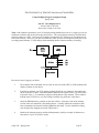
The UNIVERSITY of NORTH CAROLINA at CHAPEL HILL
Comp 541 Digital Logic & Computer Design
Spring 2010
Lab #5: VGA Display Driver
Issued Friday 2/26/2010
Report due Tuesday 3/16/2010
Task: Add a character generator to your VGA display timing module from Lab #4. I suggest you use an
architecture similar to the one shown in the picture below. The screen-character memory would be dual
ported to connect to a CPU. One port will eventually be mapped to CPU addresses so your program can
write to the memory. However, you don’t need that now (since you have not designed a CPU yet) so can
use single-ported memory. For this lab just load something into the character memory for testing.
Here are the steps I suggest you follow:
1.
First complete Lab 4 and make sure it is able to drive one of the CRT (or LCD) monitors and
display a pattern of your choice.
2.
If needed re-architect your VGA timing generator from Lab 4 to conform to the architecture
shown in the above figure. Remember that in addition to the signals shown, you will need to
keep track of the (x, y) coordinates of the pixel being drawn at any moment. These could be
tracked in the VGA Driver, or in the Timing Generator (my preference is the latter).
3.
Study the DRAM memory example on the class website. Also take a look at the memory
section of the user manual for your board/software. Carefully follow the example to learn
how to instantiate and interface with the DRAM on the board. Use the simulator to debug
your design before mapping it onto the FPGA board.
4.
Initialize the character memory and the bitmap memory with just a couple of characters at
first and see if your VGA Driver works.
Comp 541 – Spring 2010
-1-
Lab #5
5.
Add more characters and bitmaps to your design (as many as you think you might need for
your final demo in April!). You may need to think a bit into the future here, but don’t worry,
once you have the basic design working, it won’t be too hard to come back and add more
characters or bitmaps to it!
Demo: Show a working VGA Driver to instructor.
Report: Submit a hardcopy written report by Tuesday after Spring Break (March 16, 2010). The report
should include the following:
•
A block diagram (hand-drawn is fine) clearly showing the hierarchical structure of your design.
Each module in your Verilog code should be represented as a block. Each block should be
labeled with a friendly name in plain English.
Note: From now on, every lab report must include a block diagram, which may count for up to
25% of your lab score. I highly recommend that you draw this diagram even before you start
coding in Verilog! You will be evaluated for clarity, modularity, elegance, style, etc.
•
A short writeup (one para will do) stating whether your design worked, what pattern it displayed,
which monitor resolution(s) you tried, any special observations, etc.
•
A copy of the Verilog code.
•
Report the amount of FPGA resources (i.e., slices) used; you can get this from the synthesis and
place & route reports.
Comp 541 – Spring 2010
-2-
Lab #5