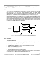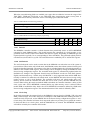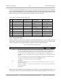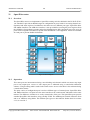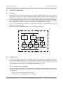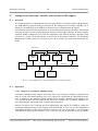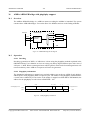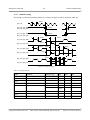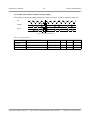
1
Quad Core LEON4 SPARC V8 Processor
LEON4-NGMP-DRAFT
Data Sheet and User’s Manual
GAISLER
Features
• Fault-tolerant quad core SPARC V8 integer unit
with 7-stage pipeline, 8 register windows, 4x4
KiB instruction and 4x4 KiB data caches.
• Double precision IEEE-754 floating point units
• CPU and I/O memory management units
• Multi-processor interrupt controller with support
for Asymmetric and Symmetric Multiprocessing
• 256 KiB Level-2 cache
• 64-bit DDR2-800 SDRAM memory interface
with Reed-Solomon EDAC
• 64-bit PC100 SDRAM memory interface with
Reed-Solomon EDAC
• 8/16-bit PROM/IO interface with EDAC
• SpaceWire router with eight SpaceWire links
• 2x 10/100/1000 Mbit Ethernet interfaces
• PCI Initiator/Target and Arbiter interface
• MIL-STD-1553B interface
• 2x UART, SPI, Timers and watchdog, 16 pin
GPIO
• Advanced on-chip debug support
Description
The LEON4-NGMP-DRAFT device
is a system-on-chip featuring a quad
core fault-tolerant LEON4 SPARC V8
processor, eight port SpaceWire
router, PCI initiator/target interface
and 10/100/1000 Mbit Ethernet
interfaces.
Specification
• System frequency: 400 MHz (TBD)
• Main memory interface: DDR2-800
SDRAM or PC100 SDRAM (TBD)
• SpaceWire router with SpaceWire links:
200 Mbit/s minimum
• 66 MHz PCI 2.3 initiator/target interface
• Ethernet 10/100/1000 Mbit MACs
• Package TBD
Applications
The LEON4-NGMP device is targeted at high-performance general
purpose payload processing. Downsized configurations of the design
are currently provided as FPGA prototypes.
Copyright Aeroflex Gaisler AB
ESA contract: 22279/09/NL/JK Deliverable: D9
May 2013, Version: Draft-2.1
AEROFLEX GAISLER
1
Overview ............................................................................................................................................... 35
Performance measurements................................................................................................................... 35
Aeroflex Gaisler GR-CPCI-XC4VLX200............................................................................................. 36
Aeroflex Gaisler GR-PCI-XC5V........................................................................................................... 37
Synopsys HAPS-51 ............................................................................................................................... 37
Synopsys HAPS-54 ............................................................................................................................... 38
TerasIC DE2-115................................................................................................................................... 39
Xilinx ML510........................................................................................................................................ 40
Special considerations............................................................................................................ 41
6.1
6.2
6.3
6.4
6.5
6.6
7
System and main memory interface clock............................................................................................. 32
SpaceWire clock .................................................................................................................................... 33
USB clock.............................................................................................................................................. 33
PCI clock ............................................................................................................................................... 33
MIL-STD-1553B clock ......................................................................................................................... 34
Clock gating unit ................................................................................................................................... 34
Debug AHB bus clocking...................................................................................................................... 34
Test mode clocking................................................................................................................................ 34
Prototype designs ................................................................................................................... 35
5.1
5.2
5.3
5.4
5.5
5.6
5.7
5.8
6
Bootstrap signals ................................................................................................................................... 27
Complete signal list ............................................................................................................................... 28
Clocking ................................................................................................................................. 32
4.1
4.2
4.3
4.4
4.5
4.6
4.7
4.8
5
Overview ............................................................................................................................................... 16
Cores...................................................................................................................................................... 18
Memory map ......................................................................................................................................... 19
Interrupts ............................................................................................................................................... 22
Plug & play information........................................................................................................................ 23
Signals.................................................................................................................................... 27
3.1
3.2
4
Scope ....................................................................................................................................................... 8
Preliminary data sheet limitations ........................................................................................................... 8
Updates and feedback.............................................................................................................................. 8
Software support...................................................................................................................................... 8
Reference documents .............................................................................................................................. 9
Document revision history .................................................................................................................... 10
Acronyms .............................................................................................................................................. 14
Definitions ............................................................................................................................................. 15
Architecture............................................................................................................................ 16
2.1
2.2
2.3
2.4
2.5
3
LEON4-NGMP-DRAFT
Introduction.............................................................................................................................. 8
1.1
1.2
1.3
1.4
1.5
1.6
1.7
1.8
2
2
GRLIB AMBA plug&play scanning..................................................................................................... 41
PROM-less systems and SpaceWire RMAP ......................................................................................... 41
System integrity and debug communication links................................................................................. 41
ASMP configurations ............................................................................................................................ 42
Software portability............................................................................................................................... 42
Level-2 cache......................................................................................................................................... 43
LEON4FT - High-performance SPARC V8 32-bit Processor ............................................... 44
Copyright Aeroflex Gaisler AB
ESA contract: 22279/09/NL/JK Deliverable: D9
May 2013, Version: Draft-2.1
AEROFLEX GAISLER
7.1
7.2
7.3
7.4
7.5
7.6
7.7
8
Overview ............................................................................................................................................... 82
Operation ............................................................................................................................................... 82
Limitations............................................................................................................................................. 83
LPDDR operation.................................................................................................................................. 84
DDR2 backend operation ...................................................................................................................... 88
SDRAM back-end operation ................................................................................................................. 90
SSRAM back-end operation.................................................................................................................. 93
Fault-tolerant operation ......................................................................................................................... 93
Fault-tolerant operation (preliminary)................................................................................................... 93
Registers ................................................................................................................................................ 96
Clocking and reset ............................................................................................................................... 104
Overview ............................................................................................................................................. 105
Operation ............................................................................................................................................. 105
Registers .............................................................................................................................................. 108
AHB/AHB bridge connecting Debug AHB bus to Processor AHB bus.............................. 111
13.1
13.2
13.3
14
Overview ............................................................................................................................................... 68
Configuration......................................................................................................................................... 68
Operation ............................................................................................................................................... 72
Registers ................................................................................................................................................ 75
AHB Memory Scrubber and Status Register ....................................................................... 105
12.1
12.2
12.3
13
Overview ............................................................................................................................................... 64
Functional description ........................................................................................................................... 64
DDRMUXCTRL - Multiplexed asynchronous DDR/SDR memory controller with ReedSolomon EDAC82
11.1
11.2
11.3
11.4
11.5
11.6
11.7
11.8
11.9
11.10
11.11
12
Floating-Point register file..................................................................................................................... 62
Floating-Point State Register (FSR)...................................................................................................... 62
Floating-Point Exceptions and Floating-Point Deferred-Queue ........................................................... 63
Level 2 Cache controller ........................................................................................................ 68
10.1
10.2
10.3
10.4
11
Overview ............................................................................................................................................... 44
LEON4 integer unit ............................................................................................................................... 46
Instruction cache.................................................................................................................................... 53
Data cache ............................................................................................................................................. 54
Additional cache functionality .............................................................................................................. 55
Memory management unit..................................................................................................................... 58
Floating-point unit ................................................................................................................................. 60
GRFPU - High-performance IEEE-754 Floating-point unit.................................................. 64
9.1
9.2
10
LEON4-NGMP-DRAFT
GRFPU Control Unit ............................................................................................................. 62
8.1
8.2
8.3
9
3
Overview ............................................................................................................................................. 111
Operation ............................................................................................................................................. 111
Registers .............................................................................................................................................. 114
LEON4 Hardware Debug Support Unit............................................................................... 115
14.1
14.2
Overview ............................................................................................................................................. 115
Operation ............................................................................................................................................. 115
Copyright Aeroflex Gaisler AB
ESA contract: 22279/09/NL/JK Deliverable: D9
May 2013, Version: Draft-2.1
AEROFLEX GAISLER
14.3
14.4
14.5
14.6
15
Overview ............................................................................................................................................. 132
Operation ............................................................................................................................................. 132
Link interface....................................................................................................................................... 133
Receiver DMA channels...................................................................................................................... 136
Transmitter DMA channels ................................................................................................................. 141
RMAP.................................................................................................................................................. 145
AMBA interface .................................................................................................................................. 150
Registers .............................................................................................................................................. 151
Overview ............................................................................................................................................. 156
Operation ............................................................................................................................................. 156
Registers .............................................................................................................................................. 157
IOMMU - AHB/AHB bridge connecting Master I/O AHB bus .......................................... 160
19.1
19.2
19.3
19.4
19.5
19.6
19.7
19.8
19.9
20
Overview ............................................................................................................................................. 130
Operation ............................................................................................................................................. 130
Registers .............................................................................................................................................. 131
AHB Trace buffer tracing Master I/O AHB bus .................................................................. 156
18.1
18.2
18.3
19
Overview ............................................................................................................................................. 128
Operation ............................................................................................................................................. 128
Registers .............................................................................................................................................. 129
SpaceWire codec with AHB host Interface and RMAP target ............................................ 132
17.1
17.2
17.3
17.4
17.5
17.6
17.7
17.8
18
AHB Trace Buffer ............................................................................................................................... 116
Instruction trace buffer ........................................................................................................................ 118
DSU memory map............................................................................................................................... 119
DSU registers....................................................................................................................................... 120
USB Debug Communication Link ....................................................................................... 130
16.1
16.2
16.3
17
LEON4-NGMP-DRAFT
JTAG Debug Link with AHB Master Interface ................................................................... 128
15.1
15.2
15.3
16
4
Overview ............................................................................................................................................. 160
Bridge operation .................................................................................................................................. 160
General access protection and address translation .............................................................................. 165
Access Protection Vector..................................................................................................................... 166
IO Memory Management Unit (IOMMU) functionality..................................................................... 168
Fault-tolerance..................................................................................................................................... 172
Statistics............................................................................................................................................... 172
ASMP support ..................................................................................................................................... 172
Registers .............................................................................................................................................. 174
Gigabit Ethernet Media Access Controller (MAC) w. EDCL ............................................. 183
20.1
20.2
20.3
20.4
20.5
20.6
20.7
20.8
Overview ............................................................................................................................................. 183
Operation ............................................................................................................................................. 183
Tx DMA interface ............................................................................................................................... 185
Rx DMA interface ............................................................................................................................... 187
MDIO Interface ................................................................................................................................... 190
Ethernet Debug Communication Link (EDCL) .................................................................................. 190
Media Independent Interfaces ............................................................................................................. 192
Registers .............................................................................................................................................. 193
Copyright Aeroflex Gaisler AB
ESA contract: 22279/09/NL/JK Deliverable: D9
May 2013, Version: Draft-2.1
AEROFLEX GAISLER
21
Overview ............................................................................................................................................. 286
Operation ............................................................................................................................................. 286
Registers .............................................................................................................................................. 290
Fault-tolerant 8/16-bit PROM/IO Memory Interface........................................................... 291
25.1
25.2
25.3
25.4
25.5
25.6
25.7
25.8
25.9
26
Overview ............................................................................................................................................. 261
Electrical interface............................................................................................................................... 261
Operation ............................................................................................................................................. 262
Bus Controller Operation .................................................................................................................... 264
Remote Terminal Operation ................................................................................................................ 269
Bus Monitor Operation........................................................................................................................ 275
Clocking and reset ............................................................................................................................... 276
Registers .............................................................................................................................................. 276
AHB/AHB bridge connecting Slave I/O AHB bus to Processor AHB bus ......................... 286
24.1
24.2
24.3
25
Overview ............................................................................................................................................. 239
Configuration....................................................................................................................................... 239
Operation ............................................................................................................................................. 244
PCI Initiator interface .......................................................................................................................... 247
PCI Target interface............................................................................................................................. 248
DMA Controller .................................................................................................................................. 250
PCI trace buffer ................................................................................................................................... 252
Interrupts ............................................................................................................................................. 253
Reset .................................................................................................................................................... 253
Registers .............................................................................................................................................. 254
MIL-STD-1553B / AS15531 Interface ................................................................................ 261
23.1
23.2
23.3
23.4
23.5
23.6
23.7
23.8
24
Overview ............................................................................................................................................. 198
Operation ............................................................................................................................................. 198
SpaceWire ports................................................................................................................................... 204
AMBA ports ........................................................................................................................................ 207
Configuration port ............................................................................................................................... 227
Registers .............................................................................................................................................. 232
32-bit PCI/AHB bridge ........................................................................................................ 239
22.1
22.2
22.3
22.4
22.5
22.6
22.7
22.8
22.9
22.10
23
LEON4-NGMP-DRAFT
SpaceWire router.................................................................................................................. 198
21.1
21.2
21.3
21.4
21.5
21.6
22
5
Overview ............................................................................................................................................. 291
PROM access....................................................................................................................................... 291
Memory mapped IO ............................................................................................................................ 293
8-bit and 16-bit PROM access............................................................................................................. 294
8- and 16-bit I/O access....................................................................................................................... 295
Burst cycles ......................................................................................................................................... 295
Memory EDAC.................................................................................................................................... 296
Bus Ready signalling........................................................................................................................... 296
Registers .............................................................................................................................................. 298
General Purpose Timer Units............................................................................................... 301
26.1
26.2
Overview ............................................................................................................................................. 301
Operation ............................................................................................................................................. 301
Copyright Aeroflex Gaisler AB
ESA contract: 22279/09/NL/JK Deliverable: D9
May 2013, Version: Draft-2.1
AEROFLEX GAISLER
26.3
27
Overview ............................................................................................................................................. 337
Multiple APB interfaces ...................................................................................................................... 338
Registers .............................................................................................................................................. 339
Overview ............................................................................................................................................. 341
Operation ............................................................................................................................................. 341
Registers .............................................................................................................................................. 342
AMBA AHB controller with plug&play support................................................................. 343
35.1
35.2
36
Overview ............................................................................................................................................. 335
Operation ............................................................................................................................................. 335
Registers .............................................................................................................................................. 336
Clock gating unit.................................................................................................................. 341
34.1
34.2
34.3
35
Overview ............................................................................................................................................. 333
Operation ............................................................................................................................................. 333
LEON4 Statistics Unit ......................................................................................................... 337
33.1
33.2
33.3
34
Overview ............................................................................................................................................. 325
Operation ............................................................................................................................................. 325
Registers .............................................................................................................................................. 328
AHB Status Registers........................................................................................................... 335
32.1
32.2
32.3
33
Overview ............................................................................................................................................. 317
Operation ............................................................................................................................................. 317
Baud-rate generation ........................................................................................................................... 319
Loop back mode .................................................................................................................................. 319
FIFO debug mode................................................................................................................................ 319
Interrupt generation ............................................................................................................................. 319
Registers .............................................................................................................................................. 320
PCI arbiter............................................................................................................................ 333
31.1
31.2
32
Overview ............................................................................................................................................. 314
Operation ............................................................................................................................................. 314
Registers .............................................................................................................................................. 315
SPI Controller supporting master and slave operation......................................................... 325
30.1
30.2
30.3
31
Overview ............................................................................................................................................. 304
Operation ............................................................................................................................................. 304
Registers .............................................................................................................................................. 308
UART Serial Interfaces ........................................................................................................ 317
29.1
29.2
29.3
29.4
29.5
29.6
29.7
30
Registers .............................................................................................................................................. 302
General Purpose I/O Port ..................................................................................................... 314
28.1
28.2
28.3
29
LEON4-NGMP-DRAFT
Multiprocessor Interrupt Controller with extended ASMP support..................................... 304
27.1
27.2
27.3
28
6
Overview ............................................................................................................................................. 343
Operation ............................................................................................................................................. 343
AMBA AHB/APB bridge with plug&play support ............................................................. 345
36.1
36.2
Overview ............................................................................................................................................. 345
Operation ............................................................................................................................................. 345
Copyright Aeroflex Gaisler AB
ESA contract: 22279/09/NL/JK Deliverable: D9
May 2013, Version: Draft-2.1
AEROFLEX GAISLER
37
LEON4-NGMP-DRAFT
Electrical description ........................................................................................................... 346
37.1
37.2
37.3
37.4
37.5
37.6
37.7
38
7
Absolute maximum ratings ................................................................................................................. 346
Operating conditions ........................................................................................................................... 346
Input voltages, leakage currents and capacitances .............................................................................. 346
Output voltages, leakage currents and capacitances............................................................................ 346
Clock Input voltages, leakage currents and capacitances.................................................................... 346
Power supplies..................................................................................................................................... 346
AC characteristics................................................................................................................................ 346
Mechanical description ........................................................................................................ 359
38.1
38.2
Component and package ..................................................................................................................... 359
Pin assignment..................................................................................................................................... 359
39
Temperature and thermal resistance..................................................................................... 372
40
Ordering information ........................................................................................................... 373
41
Open items ........................................................................................................................... 374
42
ECSS checklist..................................................................................................................... 376
Copyright Aeroflex Gaisler AB
ESA contract: 22279/09/NL/JK Deliverable: D9
May 2013, Version: Draft-2.1
AEROFLEX GAISLER
1
Introduction
1.1
Scope
8
LEON4-NGMP-DRAFT
This document is the preliminary data sheet for the Next Generation Microprocessor (NGMP). The
NGMP is being developed in an activity initiated by the European Space Agency under ESTEC contract 22279/09/NL/JK. Note that the NGMP functional prototype is described by a separate data
sheet.
The work has been performed by Aeroflex Gaisler AB, located in Göteborg, Sweden. The NGMP
architecture has been reviewed by representatives from the European Space Agency and EADS
Astrium.
1.2
Preliminary data sheet limitations
At the time of writing neither the NGMP design nor related documentation can be considered as final.
The design might be subject to changes, due to technology constraints, but also due to suggestions or
bug reports made by the first NGMP users or by other users of the IP cores used in the NGMP design.
This preliminary data sheet is primarily built up of re-used IP core documentation that has been edited
to reflect the configuration of the IP cores in the NGMP design. Parts of the documentation still give
general descriptions of IP use and has not been tailored to describe the NGMP system. Figures have in
general not been updated to instantiations in the NGMP system. Tables with timing information and
timing diagrams of signals have not been updated to reflect the current design.
1.3
Updates and feedback
Activity progress is reported at the ESA Microelectronics Section’s NGMP website:
http://microelectronics.esa.int/ngmp/ngmp.htm
Feedback and bug reports can be sent to:
Roland Wiegand, Europan Space Agency: [email protected]
Aeroflex Gaisler AB support: [email protected]
1.4
Software support
The NGMP design is supported by standard toolchains provided by Aeroflex Gaisler. Toolchains can
be downloaded from http://www.gaisler.com.
Copyright Aeroflex Gaisler AB
ESA contract: 22279/09/NL/JK Deliverable: D9
May 2013, Version: Draft-2.1
AEROFLEX GAISLER
1.5
9
LEON4-NGMP-DRAFT
Reference documents
[AMBA] AMBA Specification, Rev 2.0, ARM Limited
[GRLIB]GRLIB IP Library User's Manual, Aeroflex Gaisler, www.aeroflex.com/gaisler
[GRIP]GRLIB IP Core User's Manual, Aeroflex Gaisler, www.aeroflex.com/gaisler
[SPARC]The SPARC Architecture Manual, Version 8, SPARC International Inc.
[BLOCK] NGMP Detailed Block Diagram, NGMP-BLOCK-0001-D160, Aeroflex Gaisler
[FPDS] Quad Core LEON4 SPARC V8 Processor, Data sheet and User’s Manual,
LEON4-N2X-DS, Aeroflex Gaisler. Latest version available via ESA Microelectronics Section’s NGMP website: http://microelectronics.esa.int/ngmp/ngmp.htm
Copyright Aeroflex Gaisler AB
ESA contract: 22279/09/NL/JK Deliverable: D9
May 2013, Version: Draft-2.1
AEROFLEX GAISLER
1.6
10
LEON4-NGMP-DRAFT
Document revision history
Change record information is provided in table 1.
Table 1. Change record
Version
Date
Draft-1.0
2010 November Initial version of preliminary data sheet
Draft-1.1
2010 November First draft was not searchable. Updated description of Ethernet interface dv, er and col signals.
Draft-1.2
2011 January
Update after NGMP PDR. Updated sections: all.
Added sections on acronyms and definitions.
Created hyperlinks from memory map and register tables to register descriptions.
Added software portability section ().
Added PROM/IO interface BRDYN signal.
Added placeholder for AC section.
Removed vendor/device identifier sections.
Merged GPTIMER sections.
Merged AHBSTAT sections.
Added information on IOMMU second AHB master interface.
Renamed dsu_break signal to break and updated description.
GPIO[14] now controls if PROM EDAC checking is enabled after reset.
Updated open items list.
Draft-1.3
2011 March
Corrected table 14 (PnP for slave on Slave I/O AHB bus)
Updated description of GR-CPCI-XC4V FPGA prototype (SpW frequency)
Updated description of Xilinx ML510 prototype (quad core option)
Add description of TerasIC DE2-115 FPGA prototype
Updated DDR2 controller description with information on handling permanent device
errors.
Removed PCI trace buffer section, buffer is now included in PCI controller.
Updated PCI controller section with information on PCI trace buffer and new register interface.
Removed open item "Allow spare column of external memory".
Removed open item on L1 cache replacement policy and added note on soft configurable L1
cache replacement policy to section 7.1.2.
Removed open item concerning PCI trace buffer
Added reference to detailed block diagram.
Changed number and size of PCI BARs. Updated PCI controller section.
Updated memory map
Updated IOMMU section: page size and ASMP I/F
Added comment about BREAK signal and PROM-less booting to section 6.2.
Clarified in section 20.6.3 that low EDCL address nibbles are reset when Ethernet controllers
are reset via the clock gating unit.
Updated PROM/IO timing waveforms.
Copyright Aeroflex Gaisler AB
Note
ESA contract: 22279/09/NL/JK Deliverable: D9
May 2013, Version: Draft-2.1
AEROFLEX GAISLER
11
LEON4-NGMP-DRAFT
Table 1. Change record
Version
Date
Note
Draft-1.4
2011 June
Corrected GRIOMMU Group control register(s) documentation, bits 13:2 are not reserved.
Fix typo in description of IOMMU statistics output signal accer in table 172.
Added vendor and device ID fields to GRIOMMU master configuration registers.
Note in sections 13.2.4 and 19.2.5 that read/write combining is disabled for accesses to the
area 0xF0000000 - 0xFFFFFFFF.
Updated PCI controller section with information on re-sizable BARs, PCI target discard
timer, secondary PCI tracebuffer APB interface, drive of PCI reset and updated register
fields.
Marked pci_rst signal as bi-directional.
Increased PCI arbiter req/gnt pairs to eight pairs, updated listings in tables 21 and 426 and
description in section 31.
Updated memory map with PCI trace buffer mapped on Debug APB bus.
Corrected PnP information in tables 13, 14, 17, 18 and 19.
Added section 6.6 and added note in section 10 that L2 cache is disabled after reset.
Updated section 1: Removed multi-purpose from NGMP acronym. Added note to state that
the NGMP functional prototype is described by a separate data sheet.
Updated description of shared FPU arbitration in section 8.
Updated memory interface signal lists in tables 21 and 426, checkbit and data vectors are
now merged.
Updated signal names in Ethernet block diagram (figure 25).
Updated FT SDRAM controller open item stating that a solution is developed in the NGMP
functional prototype activity.
Updated LEON4 documentation adding FT information, added sections 7.2.9 and 7.5.5.
Also updated sections 7.1.7, 7.2.8 and 7.5.6.
Merged signals prom_data[*] and io_data[*] into promio_data[*], updated listings in tables
21 and 426 and description in section 25.
DDR2 SDRAM memory interface now makes use of three clock pairs, two clock enable and
two chip select. To accomodate (SDR) SDRAM, four chip selects and four clock enables are
used. Signal listings in tables 21 and 426 have been updated.
Draft-1.5
2011 June
Added L2 cache to feature list on front page
Added reference to NGMP functional prototype under section 5.1.
Remove remark on ML510 64-bit DDR2 limitations in section 5.8.
Closed open item on GRFPU binding, removed open item from section 41 and updated sections 2.1, 7.1.3, 7.7, 8, 9.1.
Draft-1.6
2011 August
Added MIL-STD-1553B interface; added section 23, updated tables 3, 4, 6, 15, 18, 21 and
426. Added codec clock to section 4, added section 4.5.
Added SPI interface; added section 30, updated tables 3, 4, 6, 18, 21 and 426.
Updated front page and section 2.1 to mention MIL-STD-1553B and SPI.
Update FPGA prototype section 5 with information on new interfaces.
Minor updates and fix typographical errors in sections 1.7, 1.8, 2.1, 2.3, 2.5, 3.1, 3.2, 4, 6.4
and 6.5.2.
Added new memory controller documentation; new section 11, moved description of FT
from section 12.3 to 11.3, added new SDCTRL64 documentation as section 13 and removed
previous SDCTRL section. Updated tables 3, 4 and 10.
Removed open items from section 41 on configurable SDRAM data width and FT SDRAM
controller implementation.
Updated block diagrams on front page and in section 2.1.
Added timing diagrams for SPI and MIL-STD-1553B, rearrange sections under section 37.7.
Updated SpaceWire router block diagram in section 21.1.
Copyright Aeroflex Gaisler AB
ESA contract: 22279/09/NL/JK Deliverable: D9
May 2013, Version: Draft-2.1
AEROFLEX GAISLER
12
LEON4-NGMP-DRAFT
Table 1. Change record
Version
Date
Note
Draft-1.7
2012 January
Updated section 34, clock gating unit, with information on MIL-STD-1553B clock, CPU/
FPU gating and override bit.
Corrected description of timer chaining on GPTIMER, section 26.
Changed base address of L2 cache configuration registers, updated table 4.
Remove mentions of LEON3 from sections 14.1, 27.2.2 and 37.7.1.
Updated sections 30.2.5, 30.2.6 and 30.3 with information on SPI controller slave clock filter
and SPI_SEL ignore.
Added signals mem_ifwidth and mem_clksel to signals in sections 3.1, 3.2 and 38.2.
Added mem_extclk to signals in sections 3.2 and 38.2. Updated clocking description under
section 4.
Updated description of bit 14 in table 201, Ethernet core control register.
Added note about L4STAT LOAD/STORE counting to section 33.1.
Updated base address for GRPCI2 i/f on Debug APB bus, table 5.
Updated DDR2 controller section 12 with information on registered SDRAM and technology specific fiels.
Changed wording in section 12.2.1.
Added documentation for AHB watchpoints and extended filtering under section 14,
removed open item on watchpoints.
LEON4 data cache now has 32 byte cache lines and performs 128-bit accesses for instruction
cache fills, updates under section 7.
Changed number of groups and cache/TLB size of IOMMU. Tailored section 19 to NGMP
IOMMU instantiation. Updated IOMMU open item.
Added information on IRQ(A)MP Processor boot register to section 27.
Updated L2 cache section 10 with information on error handling, error injection and internal
scrubber.
Updated PROM and IO wait states description under section 25.
Updated cache tag documentation in sections 7 and 10.
Updated L2 cache access latencies in section 10.
Various corrections of non-technical nature, see version with changebars for details.
Draft-1.8
2012 February
Corrected PCI core register descriptions under section 22.
Updated IRQ(A)MP boot register documentation under section 27.3.
Updated DDR2 controller documentation, section 12, add new register field and clarify that
ODT control register controls SDRAM-side ODT.
Fix typo "129-bit" in section 19.2.5.
Removed unresolved hyperlinks.
Tailor sections 12, 19, 25, 26, 30 and 33 to match IP core configuration used in this design.
Added read-only memory interface width field to EDAC control register in section 11.4.
Corrected address and data bus signal names in SDRAM controller section 13.
Draft-1.9
2012 April
Added information on shared FPU and clock gating to sections 8 and 34.2.
Added pci_m66en input signal, updated sections 3.2, 4.4, 22.2.2 and 38.2.
Clarified PCI reset behaviour in host mode under section 22.9.
Corrected LEON4 ASI mappings in sections 7.5.1 and 7.6.1.
Added placeholder section 39.
Copyright Aeroflex Gaisler AB
ESA contract: 22279/09/NL/JK Deliverable: D9
May 2013, Version: Draft-2.1
AEROFLEX GAISLER
13
LEON4-NGMP-DRAFT
Table 1. Change record
Version
Date
Note
Draft-2.0
2013 May
Removed "By" column in change record table.
Updated register descriptions under section 22 (PCI endianess switch field was missing).
Updated information on L1 cache replacement policy in sections 7.3.1, 7.3.2. 7.4.1 and
7.4.3.
Updated SMUL/UMUL latency in section 7.2.2 (remove mention of 16x16 multiplier).
Add paragraph about AHB watchpoint latency in DSU section 14.6.14.
Remove erroneous information about SPI controller FACT field in section 30.2.4.
Corrected address for %gn registers in DSU section 14.5.
Ethernet receive clock is 125 MHz for GMII, updated section 4.
Description of Ethernet EDCL bus select bootstrap signal values had incorrect polarity in
table 20 and section 6.3.
Updated PCI ID in section 22.2.1 and Ethernet MAC addresses in section 20.6.3. New values
apply to NGMP ASIC design and FPGA prototypes built after 2012-11-01.
Corrected LEON4 cache control register documentation, register does not have IB field.
Added description of configurable LEON4 L1 cache replacement policy.
Removed open item on LEON4 flow-through pipeline.
Add documentation on LEON4 MMU control register.
Expand LEON4 documentation with more information on types of AMBA accesses performed by the processor.
Added new memory controller documentation. Section 11 replaces earlier sections 11
(DDR2SDMUX), 12 (DDR2SPA) and 13 (SDCTRL64). Also updated memory map and
device ID tables with values/name for new memory controller.
Corrected GRFPU documentation, DZ was not listed as exception for FDIV*
Corrected GRETH GBIT MDIO PHYADDR reset values.
Noted in FTMCTRL documentation (25.7.2) that bit errors remain in external memory until
corrected by software.
Corrected BCH description in L2 cache manual from (32, 7) to (39, 32, 7)
Corrected GRSPWROUTER AHB slave base address in section 21.6.
Clarify requirements for DSU_BREAK and Break-now to have effect in section 14.2..
Documentation "tailoring" for specified NGMP system.
Corrected PCI controller documentation: GRPCI2 DMA channel control figure was missing
CID field. Fixed typo and missing bit numbers in GRPCI2 DMA control and status register
description.
Fix typo in 0xFFC00000 - 0xFFDFFFFF address range in table 4.
Draft-2.1
2013 May
Note: Document version with changebars also marks all changes made between Draft-1.9
and Draft-2.0
Update reference to NGMP functional prototype datasheet in section 1.5.
Updated text regarding functional protoype in sections 1.2 and 5.
Copyright Aeroflex Gaisler AB
ESA contract: 22279/09/NL/JK Deliverable: D9
May 2013, Version: Draft-2.1
AEROFLEX GAISLER
1.7
14
LEON4-NGMP-DRAFT
Acronyms
Table 2. Acronyms
Acronym
Comment
AHB
Advanced High-performance bus, part of [AMBA]
AMBA
Advanced Microcontroller Bus Architecture
APB
Advanced Peripheral Bus, part of [AMBA]
ASMP
Asymmetric Multi-Processing (in the context of this document: different OS instances running on own processor cores)
BCH
Bose-Hocquenghem-Chaudhuri, class of error-correcting codes
CPU
Central Processing Unit, used to refer to one LEON4 processor core.
DCL
Debug Communication Link. Provides a bridge between an external interface and on-chip
AHB bus.
DDR
Double Data Rate
DMA
Direct Memory Access
DSU
Debug Support Unit
EDAC
Error Detection and Correction
EDCL
Ethernet Debug Communication Link
FIFO
First-In-First-Out, refers to buffer type
FPU
Floating Point Unit
Gb
Gigabit, 109 bits
GB
Gigabyte, 109 bytes
GiB
Gibibyte, gigabinary byte, 230 bytes, unit defined in IEEE 1541-200
I/O
Input/Output
IP, IPv4
Internet Protocol (version 4)
ISR
Interrupt Service Routine
JTAG
Joint Test Action Group (developer of IEEE Standard 1149.1-1990)
kB
Kilobyte, 103 bytes
KiB
Kibibyte, 210 bytes, unit defined in IEEE 1541-2002
L2
Level-2, used in L2 cache abbreviation
MAC
Media Access Controller
Mb, Mbit
Megabit, 106 bits
MB, Mbyte
Megabyte, 106 bytes
MiB
Mebibyte, 220 bytes, unit defined in IEEE 1541-2002
OS
Operating System
PCI
Peripheral Component Interconnect
PROM
Programmable Read Only Memory
RAM
Random Access Memory
RMAP
Remote Memory Access Protocol
SEE
Single Event Effects
Copyright Aeroflex Gaisler AB
ESA contract: 22279/09/NL/JK Deliverable: D9
May 2013, Version: Draft-2.1
AEROFLEX GAISLER
15
LEON4-NGMP-DRAFT
Table 2. Acronyms
1.8
Acronym
Comment
SEL/SEU/
SET
Single Event Latchup/Upset/Transient
SMP
Symmetric Multi-Processing
SPARC
Scalable Processor ARChitecture
TCP
Transmission Control Protocol
UART
Universal Asynchronous Receiver/Transmitter
UDP
User Datagram Protocol
USB
Universal Serial Bus
Definitions
This section and the following subsections define the typographic and naming conventions used
throughout this document.
1.8.1
Bit numbering
The following conventions are used for bit numbering:
•
The most significant bit (MSb) of a data type has the leftmost position
•
The least significant bit of a data type has the rightmost position
•
Unless otherwise indicated, the MSb of a data type has the highest bit number and the LSb the
lowest bit number
1.8.2
Radix
The following conventions is used for writing numbers:
•
Binary numbers are indicated by the prefix "0b", e.g. 0b1010.
•
Hexadecimal numbers are indicated by the prefix "0x", e.g. 0xF00F
•
Unless a radix is explicitly declared, the number should be considered a decimal.
1.8.3
Data types
Byte (BYTE)
8 bits of data
Halfword (HWORD)
16 bits of data
Word (WORD)
32 bits of data
Double word (DWORD)
64 bits of data
Quad word (4WORD)
128-bits of data
Copyright Aeroflex Gaisler AB
ESA contract: 22279/09/NL/JK Deliverable: D9
May 2013, Version: Draft-2.1
AEROFLEX GAISLER
2
Architecture
2.1
Overview
16
LEON4-NGMP-DRAFT
The system is built around five AMBA AHB buses; one 128-bit Processor AHB bus, one 128-bit
Memory AHB bus, two 32-bit I/O AHB buses and one 32-bit Debug AHB bus. The Processor AHB
bus houses four LEON4FT processor cores connected to a shared L2 cache. The Memory AHB bus is
located between the L2 cache and the main external memory interfaces, DDR2 SDRAM and SDR
SDRAM interfaces on shared pins, and attaches a memory scrubber.
The two separate I/O AHB buses connect all peripheral cores. All slave interfaces are placed on one
bus (Slave I/O AHB bus), and all master/DMA interfaces are placed on the other bus (Master I/O
AHB bus). The Master I/O AHB bus connects to the Processor AHB bus via an AHB/AHB bridge
that provides access restriction and address translation (IOMMU) functionality. This AHB/AHB
bridge also has an AHB master interface connected to the Memory AHB bus. The AHB master interface to use when propagating traffic from a core on the Master I/O AHB bus is dynamically configurable.
The two I/O buses include all peripheral units such as timers, interrupt controllers, UARTs, general
purpose I/O port, SPI controller, MIL-STD-1553B interface, PCI master/target, High-Speed Serial
Links, Ethernet MACs, and SpaceWire router AMBA interfaces.
The fifth bus, a dedicated 32-bit Debug AHB bus, connects a debug support unit (DSU), one AHB
trace buffer monitoring the Master I/O AHB bus and several debug communication links. The Debug
AHB bus allows for non-intrusive debugging through the DSU and direct access to the complete system, as the Debug AHB bus is not placed behind an AHB bridge with access restriction functionality.
The chapters in this document have been grouped after the bus topology. The first chapters describe
cores connected to the Processor AHB bus, followed by the Memory AHB bus, Debug AHB bus,
Master I/O AHB bus and finally Slave I/O AHB bus and APB buses.
Note for preliminary datasheet: The target frequency of the LEON4FT processor cores and on-chip
buses is 400 Mhz, but depends ultimately on the final implementation technology. The clock scaling
factor to use between the memory interfaces and the on-chip system is selectable via external signals.
Copyright Aeroflex Gaisler AB
ESA contract: 22279/09/NL/JK Deliverable: D9
May 2013, Version: Draft-2.1
AEROFLEX GAISLER
17
LEON4-NGMP-DRAFT
The NGMP has the following on-chip functions:
•
•
•
•
•
•
•
•
•
•
•
•
•
•
•
•
•
•
•
•
•
•
4x LEON4 SPARC V8 processor cores with MMU and two shared GRFPU floating-point units
Level-2 cache, 4-ways, BCH protection, supports locking of 1-4 ways
Debug Support Unit (DSU) with instruction and AHB trace buffers
USB, Ethernet, JTAG and SpaceWire debug communication links
96-bit DDR2-800 SDRAM memory controller with Reed-Solomon EDAC
96-bit PC100 SDRAM memory controller with Reed-Solomon EDAC
Hardware memory scrubber
8/16-bit PROM/IO controller with BCH EDAC
I/O Memory Management Unit (IOMMU) with support for six groups of DMA units
8-port SpaceWire router/switch with four on-chip AMBA ports with RMAP
2x 10/100/1000 Mbit Ethernet MAC
32-bit 33/66 MHz PCI master/target interface with DMA engine and arbiter
MIL-STD-1553B interface controller
2x UART
SPI master/slave controller
Interrupt controller with extended support for asymmetric multiprocessing
1x Timer core with five timers and watchdog functionality
4x Timer core with four timers
Separate AHB and PCI trace buffers
Clock gating unit
LEON4 statistics unit (performance counters)
AHB status registers
A more detailed block diagram compared to what is available in this document is available in
[BLOCK].
Copyright Aeroflex Gaisler AB
ESA contract: 22279/09/NL/JK Deliverable: D9
May 2013, Version: Draft-2.1
AEROFLEX GAISLER
2.2
18
LEON4-NGMP-DRAFT
Cores
The design is based on the following cores from the GRLIB IP Library:
Table 3. Used IP cores
Core
Function
Vendor
Device
AHB2AHB
Uni-directional AHB/AHB bridge
0x01
0x020
AHBJTAG
JTAG/AHB Debug interface
0x01
0x01C
AHBSTAT
AHB Status Register
0x01
0x052
AHBTRACE
AHB trace buffer
0x01
0x017
AHBUART
Serial/AHB Debug interface
0x01
0x007
APBCTRL
AHB/APB bridge
0x01
0x006
IRQ(A)MP
Multiprocessor interrupt controller with AMP extensions
0x01
0x00D
APBUART
8-bit UART with FIFO
0x01
0x00C
DSU4
LEON4 Debug Support Unit
0x01
0x049
DDRMUXCTRL
Multiplexed asynchronous DDR/SDR memory controller
0x01
0x05D
GPTIMER
Modular timer unit with watchdog
0x01
0x011
GR1553B
MIL-STD-1553B / AS15531 interface
0x01
0x04D
GRCLKGATE
Clock gating unit
0x01
0x02C
GRETH_GBIT
10/100/1000 Ethernet MAC with DCL
0x01
0x01D
GRGPIO
General Purpose I/O Port
0x01
0x01A
GRIOMMU
AHB/AHB bridge with protection (IOMMU) functionality
0x01
0x04F
GRPCI2
Fast 32-bit PCI bridge
0x01
0x07C
GRSPW2
SpaceWire coded with AHB host interface and RMAP
0x01
0x029
GRSPWROUTER
SpaceWire router switch
0x01
0x08B
GRUSB_DCL
USB/AHB Debug interface
0x01
0x022
FTMCTRL
8/16/32-bit memory controller with EDAC
0x01
0x054
L2CACHE
Level 2 cache
0x01
0x04B
L4STAT
LEON4 statistical unit
0x01
0x047
LEON4
LEON4 SPARC V8 32-bit processor
0x01
0x048
MEMSCRUB
Memory scrubber
0x01
0x057
PCIARB
ESA PCI arbiter
0x04
0x010
RSTGEN
Reset generator
N/A
N/A
SDCTRL64
32/64-bit PC133 SDRAM controller
0x01
0x009
SPICTRL
SPI controller
0x01
0x02D
The information in the last two columns is available via plug’n’play information in the system and is
used by software to detect IP cores and to initialize software drivers.
Copyright Aeroflex Gaisler AB
ESA contract: 22279/09/NL/JK Deliverable: D9
May 2013, Version: Draft-2.1
AEROFLEX GAISLER
2.3
19
LEON4-NGMP-DRAFT
Memory map
The memory map of the internal AHB and APB buses as seen from the processor cores can be seen
below. Software does not need to be aware that a bridge is positioned between the processor and a
peripheral core since the address mapping between buses is one-to-one.
Table 4. AMBA memory map, as seen from processors
Core
Address range
Area
Bus
L2CACHE
0x00000000 - 0x7FFFFFFF
L2 cache memory area. Covers
DDR2/SDR SDRAM memory area.
Processor
GRPCI2
0x80000000 - 0xBFFFFFFF
PCI memory area
Slave I/O
FTMCTRL
0xC0000000 - 0xCFFFFFFF
PROM area
Slave I/O
0xD0000000 - 0xDFFFFFFF
Memory mapped I/O area
0xE0000000 - 0xEFFFFFFF
Unused. This memory range is occu- Processor
pied on the Debug AHB bus and is
not visible from the processors. A
separate table below shows the mapping.
0xF0000000 - 0xF03FFFFF
L2 cache configuration registers
Processor
0xF0400000 - 0xFF7FFFFF
Unused
Processor
0xFF800000 - 0xFF83FFFF
PCI I/O area
Slave I/O
L2CACHE
GRPCI2
GRIOMMU
GRSPWROUTER
0xFF840000 - 0xFF847FFF
IOMMU configuration registers
Slave I/O
0xFF848000 - 0xFF87FFFF
Unused
Slave I/O
0xFF880000 - 0xFF880FFF
SpaceWire router configuration port
Slave I/O
0xFF881000 - 0xFF8FEFFF
Unused
Slave I/O
0xFF8FF000 - 0xFF8FFFFF
Slave I/O bus plug&play area
Slave I/O
0xFF900000 - 0xFF9FFFFF
APB bridge 0
Slave I/O
APBUART0
0xFF900000 - 0xFF9000FF
UART 0 registers
Slave I/O
APBUART1
0xFF901000 - 0xFF9010FF
UART 1 registers
Slave I/O
APBBRIDGE0
GRGPIO
0xFF902000 - 0xFF9020FF
General purpose I/O port registers
Slave I/O
FTMCTRL
0xFF903000 - 0xFF9030FF
PROM/IO controller registers
Slave I/O
A
IRQ(A)MP
0xFF904000 - 0xFF907FFF
Interrupt controller registers
Slave I/O
P
GPTIMER0
0xFF908000 - 0xFF9080FF
Timer unit 0 registers
Slave I/O
B
GPTIMER1
0xFF909000 - 0xFF9090FF
Timer unit 1 registers
Slave I/O
B
GPTIMER2
0xFF90A000 - 0xFF90A0FF
Timer unit 2 registers
Slave I/O
R
GPTIMER3
0xFF90B000 - 0xFF90B0FF
Timer unit 3 registers
Slave I/O
I
GPTIMER4
0xFF90C000 - 0xFF90C0FF
Timer unit 4 registers
Slave I/O
D
GRSPWROUTER
0xFF90D000 - 0xFF90D0FF
SpaceWire router AMBA interface 0
Slave I/O
G
GRSPWROUTER
0xFF90E000 - 0xFF90E0FF
SpaceWire router AMBA interface 1
Slave I/O
E
GRSPWROUTER
0xFF90F000 - 0xFF90F0FF
SpaceWire router AMBA interface 2
Slave I/O
0
GRSPWROUTER
0xFF910000 - 0xFF9100FF
SpaceWire router AMBA interface 3
Slave I/O
GRETH_GBIT0
0xFF940000 - 0xFF94FFFF
Gigabit Ethernet MAC 0 registers
Slave I/O
GRETH_GBIT1
0xFF980000 - 0xFF98FFFF
Gigabit Ethernet MAC 1 registers
Slave I/O
APBBRIDGE0
0xFF990000 - 0xFF9FFEFF
Unused
Slave I/O
APBBRIDGE0
0xFF9FF000 - 0xFF9FFFFF
APB bus 0 plug&play area
Slave I/O
Copyright Aeroflex Gaisler AB
ESA contract: 22279/09/NL/JK Deliverable: D9
May 2013, Version: Draft-2.1
AEROFLEX GAISLER
20
LEON4-NGMP-DRAFT
Table 4. AMBA memory map, as seen from processors
Core
Address range
Area
Bus
APBBRIDGE1
0xFFA00000 - 0xFFAFFFFF
APB bridge 0
Slave I/O
A
GRPCI2
0xFFA00000 - 0xFFA000FF
PCI core registers
Slave I/O
P
PCIARB
0xFFA01000 - 0xFFA010FF
PCI arbiter registers
Slave I/O
B
GR1553B
0xFFA02000 - 0xFFA020FF
MIL-STD-1553B controller
Slave I/O
B
SPICTRL
0xFFA03000 - 0xFFA030FF
SPI controller
Slave I/O
R
GRCLKGATE
0xFFA04000 - 0xFFA040FF
Clock gating unit
Slave I/O
I
L4STAT
0xFFA05000 - 0xFFA050FF
LEON4 Statistics Unit
Slave I/O
D
AHBSTAT0
0xFFA06000 - 0xFFA060FF
AHB status register monitoring Processor AHB bus
Slave I/O
AHBSTAT1
0xFFA07000 - 0xFFA070FF
AHB status register monitoring
Slave I/O AHB bus
Slave I/O
APBBRIDGE1
0xFFA07100 - 0xFFAFFEFF
Unused
Slave I/O
APBBRIDGE1
0xFFAFF000 - 0xFFAFFFFF
APB bus 1 plug&play area
Slave I/O
0xFFB00000 - 0xFFBFFFFF
Unused
Slave I/O
0xFFC00000 - 0xFFDFFFFF
Unused
Processor
DDRMUXCTRL
0xFFE00000 - 0xFFE000FF
(DDR2/SDR) SDRAM controller
registers
Memory
MEMSCRUB
0xFFE01000 - 0xFFE010FF
Memory scrubber registers
Memory
0xFFE01100 - 0xFFEFEFFF
Unused
Memory
0xFFEFF000 - 0xFFEFFFFF
Memory bus plug&play area
Memory
0xFFF00000 - 0xFFFFEFFF
Unused
Processor
0xFFFFF000 - 0xFFFFFFFF
Processor bus plug&play area
Processor
G
E
1
When connecting to the system via one of the debug communication links (JTAG, Ethernet, USB, or
SpaceWire) connected to the Debug AHB bus, several debug support cores will be visible. Table 5
below lists the address map of these cores. Note that cores in the address range 0xE0000000 0xEFFFFFFF are not accessible from the processors or from any cores on the Master I/O AHB bus.
Accesses to this range from any core not located on the Debug AHB bus will result in an AMBA
ERROR response. Apart from the area 0xE0000000 - 0xEFFFFFFF, the AMBA memory space seen
via the debug communication links is identical to the address space seen from other cores in the system.
Table 5. AMBA address range 0xE0000000 - 0xEFFFFFFF on Debug AHB bus
Core
Address range
Comment
DSU4
0xE0000000 - 0xE07FFFFF
Debug Support Unit area for processor 0
0xE1000000 - 0xE17FFFFF
Debug Support Unit area for processor 1
0xE2000000 - 0xE27FFFFF
Debug Support Unit area for processor 2
0xE3000000 - 0xE37FFFFF
Debug Support Unit area for processor 3
0xE4000400 - 0xE40FFFFF
APB bridge on Debug AHB bus
APBBRIDGED
Copyright Aeroflex Gaisler AB
ESA contract: 22279/09/NL/JK Deliverable: D9
May 2013, Version: Draft-2.1
AEROFLEX GAISLER
21
LEON4-NGMP-DRAFT
Table 5. AMBA address range 0xE0000000 - 0xEFFFFFFF on Debug AHB bus
Core
Address range
Comment
A GRSPW2
0xE4000000 - 0xE40000FF
SpaceWire RMAP target with AMBA interface
0xE4000100 - 0xE40001FF
LEON4 Statistics unit, secondary port
B APBBRIDGED
P
L4STAT
0xE4000200 - 0xE403FFFF
Unused
D GRPCI2
0xE4040000 - 0xE407FFFF
GRPCI2 secondary PCI trace buffer interface
APBBRIDGED
0xE4080000 - 0xE40FFEFF
Unused
APBBRIDGED
0xE40FFF00 - 0xE40FFFFF
Debug APB bus plug&play area
0xE4100000 - 0xEEFFFFFF
Unused
0xEFF00000 - 0xEFF1FFFF
AHB trace buffer, tracing master I/O AHB bus
0xEFF20000 - 0xEFFFEFFF
Unused
0xEFFFF000 - 0xEFFFFFFF
Debug AHB bus plug&play area
AHBTRACE
Copyright Aeroflex Gaisler AB
ESA contract: 22279/09/NL/JK Deliverable: D9
May 2013, Version: Draft-2.1
AEROFLEX GAISLER
2.4
22
LEON4-NGMP-DRAFT
Interrupts
The table below indicates the interrupt assignments. Interrupt line 10 is used to connect to the secondary interrupt controller. All interrupts are handled by the interrupt controller and forwarded to the
LEON4 processors.
Table 6. Interrupt assignments
Interrupt
Core
Comment
1
GPTIMER0
GPTIMER unit 0, timer 1
2
GPTIMER0
GPTIMER unit 0, timer 2
3
GPTIMER0
GPTIMER unit 0, timer 3
4
GPTIMER0
GPTIMER unit 0, timer 4
5
GPTIMER0
GPTIMER unit 0, timer 5
6
GPTIMER1
Shared interrupt for all timers on GPTIMER unit 1
7
GPTIMER2
Shared interrupt for all timers on GPTIMER unit 2
8
GPTIMER3
Shared interrupt for all timers on GPTIMER unit 3
9
GPTIMER4
Shared interrupt for all timers on GPTIMER unit 4
10
IRQ(A)MP
Extended interrupt line. When one of the interrupts 1531 are asserted this interrupt is asserted to the processor(s).
11
GRPCI/PCIDMA
PCI master/target and PCI DMA
12
Unassigned
13
Unassigned
Suitable for use by software for inter-processor and
inter-process synchronization.
14
Unassigned
15
Unassigned
Note: Not maskable by processor
16
GRGPIO
17
GRGPIO
18
GRGPIO
19
GRGPIO/SPICTRL
The GPIO port has configuration registers that determine the mapping between general purpose I/O lines
and the four interrupt lines allocated to the GPIO port.
Interrupt line 19 is shared between the GPIO port and
the SPI controller.
20
SPWROUTER AMBA I/F 0
SpaceWire router AMBA interface 0
21
SPWROUTER AMBA I/F 1
SpaceWire router AMBA interface 1
22
SPWROUTER AMBA I/F 2
SpaceWire router AMBA interface 2
23
SPWROUTER AMBA I/F 3
SpaceWire router AMBA interface 3
24
GRETH_GBIT0
Gigabit Ethernet MAC 0
25
GRETH_GBIT1
Gigabit Ethernet MAC 1
26
GR1553B
MIL-STD-1553B interface controller
27
AHBSTAT
Shared by all AHB Status registers in design
28
MEMSCRUB/L2CACHE
Memory scrubber and L2 cache
29
APBUART0
UART 0
30
APBUART1
UART 1
31
GRIOMMU
IOMMU register interface interrupt.
Copyright Aeroflex Gaisler AB
ESA contract: 22279/09/NL/JK Deliverable: D9
May 2013, Version: Draft-2.1
AEROFLEX GAISLER
2.5
23
LEON4-NGMP-DRAFT
Plug & play information
The format of GRLIB AMBA Plug&play information is given in sections 35 and 36. The address
ranges of the plug&play configuration areas are given in the preceding section and is also replicated
for each core in the tables below.
The plug & play memory map and bus indexes for AMBA AHB masters on the Processor AHB bus
are shown in table 7.
Table 7. Plug & play information for masters on Processor AHB bus
Core
Index
Function
Address range
LEON4
0
LEON4 SPARC V8 Processor
0xFFFFF000 - 0xFFFFF01F
LEON4
1
LEON4 SPARC V8 Processor
0xFFFFF020 - 0xFFFFF03F
LEON4
2
LEON4 SPARC V8 Processor
0xFFFFF040 - 0xFFFFF05F
LEON4
3
LEON4 SPARC V8 Processor
0xFFFFF060 - 0xFFFFF07F
GRIOMMU
4
AHB/AHB bridge with protection functionality
0xFFFFF080 - 0xFFFFF09F
AHB2AHB
5
Uni-directional AHB/AHB bridge connecting Debug
AHB bus to Processor AHB bus
0xFFFFF0B0 - 0xFFFFF0BF
The plug & play memory map and bus indexes for AMBA AHB slaves on the Processor AHB bus are
shown in table 8.
Table 8. Plug & play information for slaves on Processor AHB bus
Core
Index
Function
Address range
L2CACHE
0
Level 2 cache
0xFFFFF800 - 0xFFFFF81F
AHB2AHB
1
Uni-directional AHB/AHB bridge connecting Processor AHB bus to Slave I/O bus
0xFFFFF820 - 0xFFFFF83F
The plug & play memory map and bus indexes for AMBA AHB masters on the Memory AHB bus are
shown in table 9.
Table 9. Plug & play information for masters on Memory AHB bus
Core
Index
Function
Address range
L2CACHE
0
Level 2 cache
0xFFEFF000 - 0xFFEFF01F
MEMSCRUB
1
Memory scrubber
0xFFEFF020 - 0xFFEFF03F
GRIOMMU
2
IOMMU secondary AHB master interface
0xFFEFF040 - 0xFFEFF05F
The plug & play memory map and bus indexes for AMBA AHB slaves on the Processor AHB bus are
shown in table 10.
Table 10. Plug & play information for slaves on Memory AHB bus
Core
Index
Function
DDRMUXCTRL
0
DDR2 SDRAM controller or SDR SDRAM controller, 0xFFEFF800 - 0xFFEFF81F
depending on the value of the mem_ifsel bootstrap signal.
MEMSCRUB
1
Memory scrubber
Copyright Aeroflex Gaisler AB
ESA contract: 22279/09/NL/JK Deliverable: D9
Address range
0xFFEFF820 - 0xFFEFF83F
May 2013, Version: Draft-2.1
AEROFLEX GAISLER
24
LEON4-NGMP-DRAFT
The plug & play memory map and bus indexes for AMBA AHB masters on the Debug AHB bus are
shown in table 11.
Table 11. Plug & play information for masters on Debug AHB bus
Core
Index
Function
Address range
AHBJTAG
0
JTAG Debug Communication Link
0xEFFFF000 - 0xEFFFF01F
GRSPW2
1
SpaceWire codes with AMBA interface and RMAP
target
0xEFFFF020 - 0xEFFFF03F
GRETH_GBIT
EDCL 0
2
10/100/1000 Mbit Ethernet Debug Communication
Link
0xEFFFF040 - 0xEFFFF05F
GRETH_GBIT
EDCL 1
3
10/100/1000 Mbit Ethernet Debug Communication
Link
0xEFFFF060 - 0xEFFFF07F
USBDCL
4
USB Debug Communication Link
0xEFFFF080 - 0xEFFFF09F
The plug & play memory map and bus indexes for AMBA AHB slaves on the Processor AHB bus are
shown in table 12.
Table 12. Plug & play information for slaves on Debug AHB bus
Core
Index
Function
Address range
DSU4
0
LEON4 Debug Support Unit
0xEFFFF800 - 0xEFFFF81F
AHB2AHB
1
Uni-directional AHB/AHB bridge connecting Debug
AHB bus to Processor AHB bus
0xEFFFF820 - 0xEFFFF83F
APBCTRL
2
AHB/APB bridge
0xEFFFF840 - 0xEFFFF85F
AHBTRACE
3
AHB trace buffer
0xEFFFF860 - 0xEFFFF87F
The plug & play memory map and bus indexes for AMBA AHB masters on the Slave I/O AHB bus
are shown in table 13.
Table 13. Plug & play information for masters on Slave I/O AHB bus
Core
Index
Function
Address range
AHB2AHB
0
Uni-directional AHB/AHB bridge connecting Processor AHB bus to Slave I/O bus
0xFF8FF000 - 0xFF8FF01F
The plug & play memory map and bus indexes for AMBA AHB slaves on the Slave I/O AHB bus are
shown in table 14.
Table 14. Plug & play information for slaves on Slave I/O AHB bus
Core
Index
Function
Address range
FTMCTRL
0
PROM/IO controller
0xFF8FF800 - 0xFF8FF81F
APBCTRL
1
AHB/APB bridge for APB bus 0
0xFF8FF820 - 0xFF8FF83F
APBCTRL
2
AHB/APB bridge for APB bus 1
0xFF8FF840 - 0xFF8FF85F
GRPCI2
3
PCI master interface
0xFF8FF860 - 0xFF8FF87F
GRIOMMU
4
IOMMU register interface
0xFF8FF880 - 0xFF8FF89F
GRSPWROUTER
5
SpaceWire router AMBA configuration interface
0xFF8FF8A0 - 0xFF8FF8BF
Copyright Aeroflex Gaisler AB
ESA contract: 22279/09/NL/JK Deliverable: D9
May 2013, Version: Draft-2.1
AEROFLEX GAISLER
25
LEON4-NGMP-DRAFT
The bus indexes for AMBA AHB masters on the Master I/O AHB bus are shown in table 15. The
Master I/O AHB bus does not have an AMBA plug&play area.
Table 15. Bus index information for masters on Master I/O AHB bus
Core
Index
Function
Address range
GRPCI2
0
PCI target
Not applicable
GRPCI2
1
PCI DMA
Not applicable
GRETH_GBIT 0
2
10/100/1000 Ethernet MAC 0
Not applicable
GRETH_GBIT 1
3
10/100/1000 Ethernet MAC 1
Not applicable
SPWROUTER
4
SpaceWire router AMBA interface 0
Not applicable
SPWROUTER
5
SpaceWire router AMBA interface 1
Not applicable
SPWROUTER
6
SpaceWire router AMBA interface 2
Not applicable
SPWROUTER
7
SpaceWire router AMBA interface 3
Not applicable
GR1553B
8
MIL-STD-1553B interface
Not applicable
The bus index for the AMBA AHB slave on the Master I/O AHB bus is shown in table 16.
Table 16. Bus index information for slaves on Master I/O AHB bus
Core
Index
Function
Address range
GRIOMMU
0
IOMMU slave interface
Not applicable
The plug & play memory map and bus indexes for AMBA APB slaves connected via the AHB/APB
bridges on the Slave I/O AHB bus are shown in tables 17 and 18.
Table 17. Plug & play information for APB slaves connected via the first APB bridge on Slave I/O AHB bus
Core
Index
Function
Address range
APBUART
0
UART 0
0xFF9FF000 - 0xFF9FF007
APBUART
1
UART 1
0xFF9FF008 - 0xFF9FF00F
GRGPIO
2
General Purpose I/O Port
0xFF9FF010 - 0xFF9FF017
FTMCTRL
3
PROM/IO memory controller
0xFF9FF018 - 0xFF9FF01F
IRQ(A)MP
4
Multiprocessor interrupt controller with AMP extension
0xFF9FF020 - 0xFF9FF027
GPTIMER
5
General Purpose Timer Unit 0
0xFF9FF028 - 0xFF9FF02F
GPTIMER
6
General Purpose Timer Unit 1
0xFF9FF030 - 0xFF9FF037
GPTIMER
7
General Purpose Timer Unit 2
0xFF9FF038 - 0xFF9FF03F
GPTIMER
8
General Purpose Timer Unit 3
0xFF9FF040 - 0xFF9FF047
GPTIMER
9
General Purpose Timer Unit 4
0xFF9FF048 - 0xFF9FF04F
GRSPWROUTER
10
SpaceWire router AMBA interface 0
0xFF9FF050 - 0xFF9FF057
GRSPWROUTER
11
SpaceWire router AMBA interface 1
0xFF9FF058 - 0xFF9FF05F
GRSPWROUTER
12
SpaceWire router AMBA interface 2
0xFF9FF060 - 0xFF9FF067
GRSPWROUTER
13
SpaceWire router AMBA interface 3
0xFF9FF068 - 0xFF9FF06F
GRETH_GBIT
14
10/100/1000 Mbit Ethernet MAC
0xFF9FF070 - 0xFF9FF077
GRETH_GBIT
15
10/100/1000 Mbit Ethernet MAC
0xFF9FF078 - 0xFF9FF07F
Copyright Aeroflex Gaisler AB
ESA contract: 22279/09/NL/JK Deliverable: D9
May 2013, Version: Draft-2.1
AEROFLEX GAISLER
26
LEON4-NGMP-DRAFT
Table 18. Plug & play information for APB slaves connected via the second APB bridge on Slave I/O AHB bus
Core
Index
Function
Address range
GRPCI2
0
PCI configuration register interface
0xFFAFF000 - 0xFFAFF007
PCIARB
1
PCI DMA configuration register interface
0xFFAFF008 - 0xFFAFF00F
GR1553B
2
MIL-STD-1553B interface
0xFFAFF010 - 0xFFAFF017
SPICTRL
3
SPI controller
0xFFAFF018 - 0xFFAFF01F
GRCLKGATE
4
Clock gating unit register interface
0xFFAFF020 - 0xFFAFF027
L4STAT
5
LEON4 Statistics Unit register interface
0xFFAFF028 - 0xFFAFF02F
AHBSTAT
6
AHB Status register interface
0xFFAFF030 - 0xFFAFF037
AHBSTAT
7
AHB Status register interface
0xFFAFF038 - 0xFFAFF03F
The plug & play memory map and bus indexes for AMBA APB slaves connected via the AHB/APB
bridge on the Debug AHB bus are shown in table 19.
Table 19. Plug & play information for APB slaves connected via APB bridge on Debug AHB bus
Core
Index
Function
Address range
GRSPW2
0
SpaceWire codec AMBA interface with RMAP target
0xE40FF000 - 0xE40FF007
L4STAT
1
LEON4 Statistics Unit
0xE40FF008 - 0xE40FF00F
GRPCI2
2
GRPCI2 trace buffer secondary interface
0xE40FF010 - 0xE40FF017
Copyright Aeroflex Gaisler AB
ESA contract: 22279/09/NL/JK Deliverable: D9
May 2013, Version: Draft-2.1
AEROFLEX GAISLER
27
3
Signals
3.1
Bootstrap signals
LEON4-NGMP-DRAFT
The power-up and initialisation state is affected by several external signals. The table below lists all
bootstrap signals.
Table 20. Bootstrap signals
Bootstrap signal
Description
DSU_EN
Enables the Debug Support Unit (DSU) and other cores on the Debug AHB bus. If DSU_EN is
HIGH the DSU and the cores on the Debug AHB bus will be clocked. If DSU_EN is LOW the DSU
and all cores on the Debug AHB bus will be clock gated off.
The value of the DSU_EN signal also controls if the Ethernet Debug Communication Links
(EDCLs) should be enabled. If DSU_EN is LOW the EDCLs will be disabled and clock gated after
reset, otherwise they will be enabled.
BREAK
Puts all processors in debug mode when asserted while DSU_EN is HIGH. When DSU_EN is LOW,
BREAK is assigned to the timer enable bit of the watchdog timer and also controls if the first processor starts executing after reset.
MEM_IFSEL
Selects the main memory interface to use. HIGH: SDR SDRAM, LOW: DDR2 SDRAM
MEM_IFFREQ
Selects the relationship between and frequencies of the system AHB clock and the memory interface
clock. See section 4.1 for a description of how the value of this signal and MEM_IFSEL selects the
clock frequencies.
MEM_IFWIDTH
Selects the width of SDR/DDR2 SDRAM interface. If this signal is low then the external memory
interface uses 64 data bits with up to 32 check bits. If this signal is high then the external memory
interface uses 32 data bits with up to 16 check bits.
MEM_CLKSEL
The value of this signal determines the clock source for the DDR2/SDR SDRAM memory. If this
signal is low then DDR2/SDR memory clock and the system clock has the same source, otherwise
the source for the DDR2/SDR memory clock is the MEM_EXTCLOCK clock input. See section 4.1
for further information.
GPIO[3:0]
Sets the least significant address nibble of the IP and MAC address for Ethernet Debug Communication Link 0.
GPIO[7:4]
Sets the least significant address nibble of the IP and MAC address for Ethernet Debug Communication Link 1.
GPIO[8]
Selects if Ethernet Debug Communication Link 0 traffic should be routed over the Debug AHB bus
(HIGH) or the Master I/O AHB bus (LOW).
GPIO[9]
Selects if Ethernet Debug Communication Link 1 traffic should be routed over the Debug AHB bus
(HIGH) or the Master I/O AHB bus (LOW).
GPIO[10]
Selects the PROM width. 0: 8-bit PROM, 1: 16-bit PROM
GPIO[11]
Signals the presence of PROM (HIGH = PROM present) and controls the clock gate settings for the
SpaceWire router. If the system lacks PROM, the PROM data bus should be held LOW to trigger an
illegal instruction trap on processor 0.
GPIO[13:12]
Sets the two least significant bits of the SpaceWire router’s instance ID.
GPIO[14]
Controls reset value of PROM/IO controller’s PROM EDAC enable (PE) bit. When this input is ’1’
at reset, EDAC checking of the PROM area will be enabled. Otherwise EDAC checking of the
PROM area will be disabled.
GPIO[15]
Used to set the USB Debug Communication Link controller into test mode. If the USB Debug Communication Link is to be used this signal must be held LOW during system reset.
Copyright Aeroflex Gaisler AB
ESA contract: 22279/09/NL/JK Deliverable: D9
May 2013, Version: Draft-2.1
AEROFLEX GAISLER
3.2
28
LEON4-NGMP-DRAFT
Complete signal list
The design has the external signals shown in table 21. The device pin assignments are available in
section 38.2.
Table 21. External signals
Name
Usage
Direction
Polarity
sys_resetn
System reset
in
Low
sys_clk
System clock
In
-
mem_extclock
Alternate clock source for SDR/DDR2 SDRAM interface
In
-
spw_clk
SpaceWire clock
In
Low
proc_errorn
Processor error mode indicator
Out-Tri
Low
break
Debug Support Unit and watchdog/processor break signal. See descrip- In
tion of bootstrap signals.
High
dsu_en
Debug Support Unit enable signal
In
High
dsu_active
Debug Support Unit active signal
Out
High
mem_ifsel
Memory interface select signal
In
-
mem_iffreq
Memory interface frequenecy select signal
In
-
mem_clksel
Memory interface external clock select signal
In
-
mem_ifwidth
Memory interface width select signal
In
-
mem_clk_fb_out
Memory interface clock feedback. DDR2 data synchronization clock,
connect this to a signal path with equal length of the DDR2 CLK trace +
DDR2 DQS trace
Out
-
mem_clk_fb
Memory interface clock feedback. DDR2 data synchronization clock,
connect this to the other end of the signal path connected to
MEM_CLK_FB_OUT
In
-
mem_clk_p[2:0]
SDRAM clock / DDR memory clocks (positive)
Out
-
mem_clk_n[2:0]
DDR memory clocks (negative)
Out
-
mem_wen
Memory write enable
Out
Low
mem_sn[3:0]
Memory chip select
Out
Low
mem_rasn
Memory row address strobe
Out
Low
mem_odt[1:0]
Memory ODT
Out
High
mem_dqs_p[11:0]
DDR2 memory data strobe
BiDir
-
mem_dqs_n[11:0]
DDR2 memory data strobe (inverted)
BiDir
-
mem_dqm[11:0]
Memory data mask
Out
Low
mem_dq[95:0]
Memory data and checkbit bus
BiDir
-
mem_cke[3:0]
Memory interface clock enable
Out
High
mem_casn
Memory column address strobe
Out
Low
mem_ba[2:0]
Memory bank address
Out
-
mem_addr[14:0]
Memory address
Out
-
jtag_tck
JTAG Debug Communication Link Clock
In
-
jtag_tms
JTAG Debug Communication Link Mode select
In
-
jtag_tdi
JTAG Debug Communication Link Data in
In
-
jtag_tdo
JTAG Debug Communication Link Data out
Out
-
jtag_trst
JTAG Debug Communication Link Reset
In
-
Copyright Aeroflex Gaisler AB
ESA contract: 22279/09/NL/JK Deliverable: D9
May 2013, Version: Draft-2.1
AEROFLEX GAISLER
29
LEON4-NGMP-DRAFT
Table 21. External signals
Name
Usage
Direction
Polarity
usb_clk
USB Debug Communication Link ULPI Clock
In
-
usb_nxt
USB Debug Communication Link ULPI Next
In
High
usb_dir
USB Debug Communication Link ULPI Direction
In
-
usb_d[7:0]
USB Debug Communication Link ULPI Data
BiDir
-
usb_resetn
USB Debug Communication Link ULPI Reset
Out
Low
usb_stp
USB Debug Communication Link ULPI Stop
Out
High
spwd_txd
SpaceWire Debug Communication Link transmit data
Out
-
spwd_txs
SpaceWire Debug Communication Link transmit strobe
Out
-
spwd_rxd
SpaceWire Debug Communication Link receive data
In
-
spwd_rxs
SpaceWire Debug Communication Link receive strobe
In
-
eth0_txer
Ethernet port 0, Transmit error
Out
High
eth0_txd[7:0]
Ethernet port 0, Transmitter output data
Out
-
eth0_txen
Ethernet port 0, Transmitter enable
Out
High
eth0_gtxclk
Ethernet port 0, Gigabit clock
In
-
eth0_txclk
Ethernet port 0, Transmitter clock
In
-
eth0_rxer
Ethernet port 0, Receive error
In
High
eth0_rxd[7:0]
Ethernet port 0, Receiver data
In
-
eth0_rxdv
Ethernet port 0, Receive data valid
In
High
eth0_rxclk
Ethernet port 0, receiver clock
In
-
eth0_mdio
Ethernet port 0, Management Interface Data Input/Output
BiDir
-
eth0_mdc
Ethernet port 0, Management Interface Data Clock
Out
-
eth0_col
Ethernet port 0, Collision detected
In
High
eth0_crs
Ethernet port 0, Carrier sense
In
High
eth0_mdint
Ethernet port 0, Management Interface Interrupt
In
Low
eth1_txer
Ethernet port 1, Transmit error
Out
High
eth1_txd[7:0]
Ethernet port 1, Transmitter output data
Out
-
eth1_txen
Ethernet port 1, Transmitter enable
Out
High
eth1_gtxclk
Ethernet port 1, Gigabit clock
In
-
eth1_txclk
Ethernet port 1, Transmitter clock
In
-
eth1_rxer
Ethernet port 1, Receive error
In
High
eth1_rxd[7:0]
Ethernet port 1, Receiver data
In
-
eth1_rxdv
Ethernet port 1, Receive data valid
In
High
eth1_rxclk
Ethernet port 1, receiver clock
In
-
eth1_mdio
Ethernet port 1, Management Interface Data Input/Output
BiDir
-
eth1_mdc
Ethernet port 1, Management Interface Data Clock
Out
-
eth1_col
Ethernet port 1, Collision detected
In
High
eth1_crs
Ethernet port 1, Carrier sense
In
High
eth1_mdint
Ethernet port 1, Management Interface Interrupt
In
Low
spw_txd[7:0]
SpaceWire router ports 1 - 8, transmit data
Out
-
spw_txs[7:0]
SpaceWire router ports 1 - 8, transmit strobe
Out
-
spw_rxd[7:0]
SpaceWire router ports 1 - 8, receive data
In
-
Copyright Aeroflex Gaisler AB
ESA contract: 22279/09/NL/JK Deliverable: D9
May 2013, Version: Draft-2.1
AEROFLEX GAISLER
30
LEON4-NGMP-DRAFT
Table 21. External signals
Name
Usage
Direction
Polarity
spw_rxs[7:0]
SpaceWire router ports 1 - 8, receive strobe
In
-
pci_clk
PCI clock
In
-
pci_gnt
PCI grant
In
Low
pci_idsel
PCI Device select during configuration
In
High
pci_hostn
PCI System host. Low = Device will act as PCI host
In
Low
pci_rst
PCI reset
BiDir
Low
pci_ad[31:0]
PCI Address and Data bus
BiDir
High
pci_cbe[3:0]
PCI Bus command and byte enable
BiDir
Low
pci_frame
PCI Cycle frame
BiDir
Low
pci_irdy
PCI Initiator ready
BiDir
Low
pci_trdy
PCI Target ready
BiDir
Low
pci_devsel
PCI Device select
BiDir
Low
pci_stop
PCI Stop
BiDir
Low
pci_perr
PCI Parity error
BiDir
Low
pci_serr
PCI System error
BiDir
Low
pci_par
PCI Parity signal
BiDir
High
pci_inta
PCI Interrupt A
BiDir
Low
pci_intb
PCI Interrupt B
In
Low
pci_intc
PCI Interrupt C
In
Low
pci_intd
PCI Interrupt D
In
Low
pci_req
PCI Request signal
Out
Low
pci_m66en
PCI 66 MHz enable signal
In
High
pci_arb_req[7:0]
PCI arbiter request
In
Low
pci_arb_gnt[7:0]
PCI arbiter grant
Out
Low
prom_cen[1:0]
PROM chip select
Out
Low
promio_addr[27:0]
PROM/IO address
Out
-
promio_oen
PROM/IO Output Enable
Out
Low
promio_wen
PROM/IO Write Enable
Out
Low
promio_brdyn
PROM/IO Bus ready
In
Low
promio_data[15:0]
PROM/IO data
BiDir
-
io_sn
PROM/IO chip select
Out
Low
wdogn
Watchdog output
Bidir
Low
gpio[15:0]
General Purpose I/O
Bidir
-
uart0_txd
UART 0, transmit data
Out
-
uart0_rxd
UART 0, receive data
In
-
uart0_rtsn
UART 0, request to sent
Out
Low
uart0_ctsn
UART 0, clear to send
In
Low
uart1_txd
UART 1, transmit data
Out
-
uart1_rxd
UART 1, receive data
In
-
uart1_rtsn
UART 1, request to sent
Out
Low
uart1_ctsn
UART 1, clear to send
In
Low
Copyright Aeroflex Gaisler AB
ESA contract: 22279/09/NL/JK Deliverable: D9
May 2013, Version: Draft-2.1
AEROFLEX GAISLER
31
LEON4-NGMP-DRAFT
Table 21. External signals
Name
Usage
Direction
Polarity
gr1553_busarxen
MIL-STD-1553 Bus A receiver enable
Out
High
gr1553_busarxp
MIL-STD-1553 Bus A receiver positive input
In
High
gr1553_busarxn
MIL-STD-1553 Bus A receiver negative input
In
High
gr1553_busatxin
MIL-STD-1553 Bus A transmitter inhibit
Out
High
gr1553_busatxp
MIL-STD-1553 Bus A transmitter positive output
Out
High
gr1553_busatxn
MIL-STD-1553 Bus A transmitter negative output
In
High
gr1553_busbrxen
MIL-STD-1553 Bus B receiver enable
Out
High
gr1553_busbrxp
MIL-STD-1553 Bus B receiver positive input
In
High
gr1553_busbrxn
MIL-STD-1553 Bus B receiver negative input
In
High
gr1553_busbtxin
MIL-STD-1553 Bus B transmitter inhibit
Out
High
gr1553_busbtxp
MIL-STD-1553 Bus B transmitter positive output
Out
High
gr1553_busbtxn
MIL-STD-1553 Bus B transmitter negative output
Out
High
gr1553_clk
MIL-STD-1553 interface clock
In
-
spi_miso
SPI controller, master input, slave output
BiDir
-
spi_mosi
SPI controller, master output, slave input
BiDir
-
spi_sck
SPI controller, clock
BiDir
-
spi_sel
SPI controller, SPI select
In
Low
spi_slvsel[1:0]
SPI controller, slave select
Out
Low
testen
Test enable signal
In
High
Copyright Aeroflex Gaisler AB
ESA contract: 22279/09/NL/JK Deliverable: D9
May 2013, Version: Draft-2.1
AEROFLEX GAISLER
4
32
LEON4-NGMP-DRAFT
Clocking
The table below specifies the clock inputs to the device.
Table 22. Clock inputs
Clock input
Description
Recommended frequency
SYS_CLK
System clock input
100 MHz
MEM_EXTCLK
Alternate clock source for memory interface clock
100 MHz
SPW_CLK
SpaceWire clock
50 MHz
MEM_CLK_FB
Feedback clock for (DDR) SDRAM memory interface
-
JTAG_TCK
JTAG Debug Communication Link clock
10 MHz (max, TBD)
USB_CLK
USB Debug Communication Link clock
60 MHz
ETH0_GTXCLK
Ethernet Gigabit MAC 0 clock
125 MHz
ETH0_TXCLK
Ethernet MAC 0 transmit clock
25 MHz
ETH0_RXCLK
Ethernet MAC 0 receive clock
25 MHz (MII)
125 MHz (GMII)
ETH1_GTXCLK
Ethernet Gigabit MAC 1 clock
125 MHz
ETH1_TXCLK
Ethernet MAC 1 transmit clock
25 MHz
ETH1_RXCLK
Ethernet MAC 1 receive clock
25 MHz (MII)
125 MHz (GMII)
PCI_CLK
PCI interface clock
66 or 33 MHz
GR1553_CLK
MIL-STD-1553B interface clock
20 MHz
The design makes use of clock multipliers to create the system clock, memory interface clock, and the
SpaceWire transmitter clock. The system clock (AHB clock), and the memory interface clock are
connected through clock multiplexers in order to select between clock options for the two different
memory interfaces.
4.1
System and main memory interface clock
The system clock is used to clock the processors, the AMBA buses, and all on-chip cores. The system
clock frequency depends on the setting of the bootstrap signals MEM_IFSEL and MEM_IFFREQ.
The SDR/DDR2 memory interface clock depends on the signals MEM_IFSEL, MEM_IFREQ and
MEM_CLKSEL. The last signal, MEM_CLKSEL, selects if the memory interface clock should be
generated from the same source as the AMBA clock (SYS_CLK input) or an alternate clock source
(MEM_EXTCLK input).
Table 23 shows how the system is clocked depending on the MEM_CLKSEL, MEM_IFSEL and
MEM_IFFREQ signals. Note that the only signal affecting the (AMBA) system frequency is
MEM_IFFREQ.
Copyright Aeroflex Gaisler AB
ESA contract: 22279/09/NL/JK Deliverable: D9
May 2013, Version: Draft-2.1
AEROFLEX GAISLER
33
LEON4-NGMP-DRAFT
Table 23. Clock selection
MEM_CLKSEL
MEM_IFSEL
Low
Low
MEM_IFFREQ Description
Low
Memory interface is DDR2 SDRAM, both memory interface
and system are clocked with the same clock.
System clock: 4x SYS_CLK input
Memory interface clock: 4x SYS_CLK input
High
Memory interface is DDR2 SDRAM, system clock frequency
is half of the memory interface clock frequency.
System clock: 2x SYS_CLK input
Memory interface clock: 4x SYS_CLK input
Low
Memory interface is (SDR) SDRAM, system clock frequency
is four times higher than the memory interface clock frequency.
System clock: 4x SYS_CLK input
Memory interface clock: 1x SYS_CLK input
High
Memory interface is (SDR) SDRAM, both memory interface
and system are clocked with same clock.
System clock: 2x SYS_CLK input
Memory interface clock: 2x SYS_CLK input
Low
Memory interface is DDR2 SDRAM, clocks are asynchronous.
System clock: 4x SYS_CLK input
Memory interface clock: 4x MEM_EXTCLK input
High
Memory interface is DDR2 SDRAM, clocks are asynchronous
System clock: 2x SYS_CLK input
Memory interface clock: 4x MEM_EXTCLK input
Low
Memory interface is (SDR) SDRAM, clocks are asynchronous.
System clock: 4x SYS_CLK input
Memory interface clock: MEM_EXTCLK input
High
Memory interface is (SDR) SDRAM, clocks are asynchronous.
System clock: 2x SYS_CLK input
Memory interface clock: MEM_EXTCLK input
High
Low
High
High
4.2
SpaceWire clock
The clock used for the SpaceWire links’ receiver and transmitter logic is taken from the dedicated
SpaceWire clock pin spw_clk and is multiplied on-chip.
4.3
USB clock
The clock used to clock the serial interface engine in the USB debug communication link is taken
from the dedicated clock pin usb_clk. The input frequency required by the ULPI interface is 60 MHz.
4.4
PCI clock
The PCI clock is taken from the dedicated clock pin pci_clk. The device is capable of 33 MHz and 66
MHz operation. The input signal pci_m66en must reflect the frequency of the input PCI clock.
pci_m66en should be HIGH if the PCI clock is a 66 MHz clock and LOW if the PCI clock frequency
is 33 MHz.
Copyright Aeroflex Gaisler AB
ESA contract: 22279/09/NL/JK Deliverable: D9
May 2013, Version: Draft-2.1
AEROFLEX GAISLER
4.5
34
LEON4-NGMP-DRAFT
MIL-STD-1553B clock
The 20 MHz clock for the MIL-STD-1553B codec is taken from the dedicated pin gr1553b_clk.
4.6
Clock gating unit
The design has a clock gating unit through which individual cores can have their AHB clocks enabled/
disabled and resets driven. The cores connected to the clock gating unit are listed in the table below.
Table 24. Devices with gatable clock
Device
Ethernet MAC 0
Ethernet MAC 1
SpaceWire router
PCI Target/Initiator and PCI DMA unit
MIL-STD-1553B interface controller
The LEON4 processor cores will automatically be clock gated when the processor enters power-down
or halt state. The floating-point units (GRFPU) will be clock gated when the corresponding processor
has disabled FPU operations by setting the %psr.ef bit to zero, or when the processor has entered
power-down/halt mode.
The Ethernet MAC cores are gated off after reset unless the Debug Support Unit is enabled via the
DSU_EN signal. The SpaceWire router is disabled after reset unless general purpose I/O line 11
(GPIO[11]) signals a prom-less system. The PCI cores are always enabled after reset.
For more information see the chapter about the clock gating unit.
4.7
Debug AHB bus clocking
All cores on the Debug AHB bus will be gated off when the DSU_EN signal is low.
4.8
Test mode clocking
When in test mode (testen signal = 1) all clocks in the design are connected to the SYS_CLK test
clock.
Copyright Aeroflex Gaisler AB
ESA contract: 22279/09/NL/JK Deliverable: D9
May 2013, Version: Draft-2.1
AEROFLEX GAISLER
5
Prototype designs
5.1
Overview
35
LEON4-NGMP-DRAFT
Several prototype designs of NGMP are available. The subsections below describe how the prototype
designs differ from the design described by this document.
FPGA prototype designs are available for the boards listed in table 25 below.
Table 25. Boards with NGMP prototype designs
Board
Section
Comment
Aeroflex Gaisler GR-CPCI-XC4VLX200
5.3
Quad core system with SpaceWire and PCI.
Aeroflex Gaisler GR-PCI-XC5V
5.4
Single core system with SpaceWire, PCI and USB.
Synopsys HAPS-51
5.5
Quad core system. Limited IO interfaces.
Synopsys HAPS-54
5.6
Quad core system. Limited IO interfaces.
TerasIC DE2-115
5.7
Dual or quad core system. Limited IO interfaces.
Xilinx ML510
5.8
Dual core system or quad core system. PCI but otherwise limited in IO interfaces.
The configuration descriptions below may include omissions and may become outdated. Please contact Aeroflex Gaisler to verify that a particular prototype design provides the needed functionality
before placing an order. Clock gating is disabled for all prototype design but can be enabled on
request. FPGA prototype designs include the LEON4 processor but not the fault-tolerant LEON4FT
processor.
A NGMP functional prototype device together with a validation board is available from Aeroflex
Gaisler. The product page is available at http://www.gaisler.com/gr-cpci-leon4-n2x.
5.2
Performance measurements
The NGMP system connects the DMA capable peripheral I/O units via an IOMMU. In order for the
DMA units to access external main memory, traffic must pass through the IOMMU and L2 cache.
Both bridges add latency to each access or block of accesses. The design of the NGMP system relies
on the system frequency being high enough so that these added latencies are small relative to the
latency from external memory devices. On a FPGA prototype system the latencies from traversing the
IOMMU and L2 cache become highly noticeable. The FPGA prototypes are therefore not suitable for
performing I/O throughput measurements without also scaling external bandwidth. For instance, a
throughput test using TCP/IP on a 1000 Mbit Ethernet link will show poor performance on the prototype system due to packet drops. In this case, forcing the link to 100 Mbit and then scaling the results
should give a more accurate view of final system performance.
When scaling results for processor performance measurements, Level 2 cache hit rate must be taken
into account. The final system will likely include a larger Level 2 cache than what the FPGA prototype designs have and hit rate may be improved. When scaling results it is important to notice that the
performance of the external memory interface does not scale linearly with system frequency. The
external (DDR2) SDRAM has latencies that do not change with increased memory interface frequency.
Copyright Aeroflex Gaisler AB
ESA contract: 22279/09/NL/JK Deliverable: D9
May 2013, Version: Draft-2.1
AEROFLEX GAISLER
5.3
36
LEON4-NGMP-DRAFT
Aeroflex Gaisler GR-CPCI-XC4VLX200
The NGMP prototype design for GR-CPCI-XC4VLX200 features a quad core LEON4 system with a
single shared FPU. Table 26 below lists the differences in the GR-CPCI-XC4VLX200 design compared to the system described by this data sheet.
Table 26. GR-CPCI-XC4VLX200 description
Parameter
Comment
System frequency
45 MHz
SpaceWire link clock frequency
200 MHz
Clock gating
Disabled. Clock gating unit is not present.
Floating point unit
One GRFPU floating point unit is shared between all four processor cores.
L2 cache EDAC
L2 cache is not protected by ECC. Timing of FT L2 cache is emulated.
Main memory interface
Main memory interface is SDRAM without check bits. DDR2 SDRAM is
not available.
SpaceWire codec on Debug AHB bus
SpaceWire codec on Debug AHB bus is not implemented
USB Debug communication link
USB DCL is not available
Ethernet
The system has one 10/100 Mbit Ethernet MAC
SpaceWire router
SpaceWire router has 4 external SpaceWire links
SPI controller
Not available
MIL-STD-1553B
Can be made available using a GR-ACC-1553 or GR-CPCI-1553 mezzanine.
GR-CPCI-XC4VLX200 boards with the described NGMP prototype design can be ordered from Aeroflex Gaisler. The kit consists of a GR-CPCI-XC4VLX200 board and a GR-SER2-SPW4 mezzanine.
Copyright Aeroflex Gaisler AB
ESA contract: 22279/09/NL/JK Deliverable: D9
May 2013, Version: Draft-2.1
AEROFLEX GAISLER
5.4
37
LEON4-NGMP-DRAFT
Aeroflex Gaisler GR-PCI-XC5V
The NGMP prototype design for GR-PCI-XC5V has a single processor core with FPU. The primary
use of the design is for validation of the USB Debug Communication Link. Table 27 below lists the
differences in the GR-PCI-XC5V design compared to the system described by this data sheet.
Table 27. GR-PCI-XC5V description
5.5
Parameter
Comment
System frequency
60 MHz
SpaceWire link clock frequency
60 MHz
Clock gating
Disabled. Clock gating unit is not present.
Processor
The design has one LEON4 processor core
Floating point unit
The design does not have a FPU
L2 cache
L2 cache is not protected by ECC and has 16 KiB per way.
Main memory interface
Main memory interface is SDRAM without check bits. DDR2 SDRAM is
not available.
General Purpose I/O port
The design has eight lines of the GPIO port connected to external ports
SpaceWire codec on Debug AHB bus
SpaceWire codec on Debug AHB bus is not implemented
Ethernet
The system has one 10/100/1000 Mbit Ethernet MAC
SPI controller
Not available
MIL-STD-1553B
Can be made available using a GR-ACC-1553 mezzanine.
Synopsys HAPS-51
The NGMP prototype design for HAPS-51 features a quad core LEON4 system with two shared
FPUs. The standard design makes use of the HAPS-51 on-board DDR2 SDRAM interface. If
requested, it is possible to extend this to include SDRAM via the SDRAM_1x1 daughter board from
Synopsys. Table 28 below lists the differences in the HAPS-51 design compared to the system
described by this data sheet.
Table 28. HAPS-51 description
Parameter
Comment
System frequency
50 MHz
Clock gating
Disabled. Clock gating unit is not present.
Main memory interface
Main memory interface is DDR2-300 without EDAC. (SDR) SDRAM is not
available, see text above.
SpaceWire codec on Debug AHB bus
SpaceWire codec on Debug AHB bus is not implemented
USB Debug communication link
USB DCL is not available
PCI
PCI trace buffer is not available. PCI arbiter is not available. PCI initiator/
target is not available.
General Purpose I/O port
General purpose I/O lines are not connected to external pins
SpaceWire router
SpaceWire router is implemented but has no external SpaceWire links
SPI controller
Not available
MIL-STD-1553B
Not available
Aeroflex Gaisler does not provide Synopsys HAPS-51 boards but can provide bit streams.
Copyright Aeroflex Gaisler AB
ESA contract: 22279/09/NL/JK Deliverable: D9
May 2013, Version: Draft-2.1
AEROFLEX GAISLER
5.6
38
LEON4-NGMP-DRAFT
Synopsys HAPS-54
The NGMP prototype design for HAPS-54 features a quad core LEON4 system with two shared
FPUs. The standard design makes use of the Synopsys SDRAM_1x1 daughter board interface. Table
29 below lists the differences in the HAPS-54 design compared to the system described by this data
sheet.
Table 29. HAPS-54 description
Parameter
Comment
System frequency
50 MHz
Clock gating
Disabled. Clock gating unit is not present.
Main memory interface
Main memory interface is (SDRAM) without EDAC. DDR2 SDRAM is not
available.
SpaceWire codec on Debug AHB bus
SpaceWire codec on Debug AHB bus is not implemented
USB Debug communication link
USB DCL is not available
PCI
PCI trace buffer is not available. PCI arbiter is not available. PCI initiator/
target is not available.
General Purpose I/O port
General purpose I/O lines are not connected to external pins
SpaceWire router
SpaceWire router is implemented but has no external SpaceWire links
SPI controller
Not available
MIL-STD-1553B
Not available
Aeroflex Gaisler does not provide Synopsys HAPS-54 boards but can provide bit streams.
Copyright Aeroflex Gaisler AB
ESA contract: 22279/09/NL/JK Deliverable: D9
May 2013, Version: Draft-2.1
AEROFLEX GAISLER
5.7
39
LEON4-NGMP-DRAFT
TerasIC DE2-115
The NGMP prototype design for TerasIC DE2-115 has two processor cores with one shared FPU.
Table 30 below lists the differences in the DE2-115 design compared to the system described by this
data sheet.
Table 30. DE2-115 description
Parameter
Comment
System frequency
50 MHz
Clock gating
Disabled. Clock gating unit is not present.
Processor
Has two LEON4 processor cores
Floating point unit
One GRFPU floating point unit is shared between the two processor cores.
L2 cache EDAC
L2 cache is not protected by ECC. Timing of FT L2 cache is emulated. L2
cache has four ways of 32 KiB.
Main memory interface
Main memory interface is 32-bit SDRAM without EDAC. DDR2 SDRAM
is not available.
SpaceWire codec on Debug AHB bus
SpaceWire codec on Debug AHB bus is not implemented
USB Debug communication link
USB DCL is not available
General purpose I/O port
Design has 16 GPIO lines
Ethernet
The system has one 1000 Mbit Ethernet MAC, running in 10/100 mode.
SpaceWire router
The SpaceWire router is not implemented
SPI controller
Not available
MIL-STD-1553B
Not available
Copyright Aeroflex Gaisler AB
ESA contract: 22279/09/NL/JK Deliverable: D9
May 2013, Version: Draft-2.1
AEROFLEX GAISLER
5.8
40
LEON4-NGMP-DRAFT
Xilinx ML510
The NGMP prototype design for ML510 is available in two configurations; one with two processor
cores and a shared FPU, and one with four processor cores without a FPU. Table 31 below lists the
differences in the ML510 design compared to the system described by this data sheet.
Table 31. ML510 description
Parameter
Comment
System frequency
70 MHz
Clock gating
Disabled. Clock gating unit is not present.
Processor
Has two, or four, LEON4 processor cores
Floating point unit
One, or zero, GRFPU floating point unit is shared between the two processor
cores.
L2 cache EDAC
L2 cache is not protected by ECC. Timing of FT L2 cache is emulated.
Main memory interface
Main memory interface is 32-bit DDR2-280 SDRAM with EDAC. Designs
using 64-bit DDR2 without EDAC can also be produced on request. (SDR)
SDRAM is not available.
SpaceWire codec on Debug AHB bus
SpaceWire codec on Debug AHB bus is not implemented
USB Debug communication link
USB DCL is not available
General purpose I/O port
Design has three GPIO lines on external pins, connected to a DIP switch.
Ethernet
The system has one 10/100 Mbit Ethernet MAC
SpaceWire router
The SpaceWire router is not implemented
SPI controller
Available
MIL-STD-1553B
Not available
Copyright Aeroflex Gaisler AB
ESA contract: 22279/09/NL/JK Deliverable: D9
May 2013, Version: Draft-2.1
AEROFLEX GAISLER
41
6
Special considerations
6.1
GRLIB AMBA plug&play scanning
LEON4-NGMP-DRAFT
The bus structure in this design requires some special consideration with regard to plug&play scanning. The default behavior of GRLIB AMBA plug&play scanning routines is to start scanning at
address 0xFFFFF000. If any AHB/AHB bridges, APB bridges or L2 cache controllers are detected
during the scan, the general scanning routine traverses the bridge and reads the plug&play information from the bus behind the bridge. In this design, the default 0xFFFFF000 address gives plug&play
information for the Processor AHB bus. This plug&play area contains information which allows software to detect all devices on the Processor, Slave I/O, Master I/O and Memory AHB buses.
The plug&play information on the Processor bus does not contain any references to the plug&play
information on the Debug AHB bus, nor can the cores on the Debug AHB bus be accessed from the
Processor AHB bus as the buses are connected using a uni-directional bridge. In order to detect the
cores on the Debug AHB bus, the debug monitor used must be informed about the memory map of the
bus, or be instructed to start plug&play scanning at address 0xEFFFF000 from where all the other
plug&play areas in the system can be found.
Depending on the debug monitor used, the monitor may detect that it connects to a NGMP design and
start scanning on the Debug AHB bus. Otherwise the address 0xEFFFF000 should be specified to the
monitor. In the case where the monitor detects that it is connected to a NGMP design, it may be necessary to force the monitor to start scanning at the default address 0xFFFFF000 when connecting with
a debug monitor through the Master I/O bus, from which the Debug AHB bus cannot be accessed.
6.2
PROM-less systems and SpaceWire RMAP
The system has support for PROM less operation where system software is uploaded by an external
entity. In order to allow system software to be uploaded via RMAP the bootstrap signal GPIO[11]
should be low in order to not clock gate off the SpaceWire router after system reset. The IOMMU will
be in pass-through after reset allowing an external entity to upload software, change the processor
reset start address, and wake the processors up via the multiprocessor interrupt controller’s register
interface. In order to prevent the processor from starting execution, the external BREAK signal should
be asserted. This will also prevent the system’s watchdog timer from being started.
If the system has a boot PROM available it is recommended to have the SpaceWire router gated off
after reset by setting the bootstrap signal GPIO[11] high during system reset. If router functionality
needs to be immediately available, the designer should consider disabling RMAP or enable IOMMU
protection early in the software boot process so that external entities cannot interfere with system
operation. It takes 20 microseconds for the SpaceWire links to enter run state. Before that, incoming
RMAP traffic cannot enter the system. This leaves time (8000 cycles at 400 MHz system frequency)
for the processors to disable RMAP via a register write, or to set up rudimentary IOMMU protection.
6.3
System integrity and debug communication links
The debug communication links have unrestricted access to all parts of the system. When the Debug
AHB bus is clock gated off via the external dsu_en signal, all debug communication links will be disabled. However, the Ethernet Debug Communication Links (EDCLs) can still be enabled via the
Ethernet controllers’ register interfaces. Since the Debug AHB bus is gated off, the only path for
EDCL traffic into the system is through the IOMMU. Since EDCL traffic flows through the same
AHB master interface as normal Ethernet traffic the IOMMU may not provide adequate protection. To
Copyright Aeroflex Gaisler AB
ESA contract: 22279/09/NL/JK Deliverable: D9
May 2013, Version: Draft-2.1
AEROFLEX GAISLER
42
LEON4-NGMP-DRAFT
ensure that EDCL traffic cannot be harmful, even if accidentally enabled, it is recommended to tie
GPIO[9:8] HIGH during system reset in order to force EDCL traffic onto the gated Debug AHB bus.
6.4
ASMP configurations
The system supports running different OS instances on each of the processor cores. The use of ASMP
configurations is eased by:
•
The multiprocessor interrupt controller that contains four internal interrupt controllers. This
means that each OS (up to four) can have direct access to its own interrupt controller. It is also
possible to run two SMP operating systems simultaneously.
•
The availability of several general purpose timer units allows each OS to have a dedicated timer
unit.
•
All peripheral registers are mapped on 4 KiB address boundaries. This allows using the system’s
memory management units to provide separation between operating systems.
•
The I/O memory management unit (IOMMU) can prevent DMA capable peripheral controllers
belonging to one OS from overwriting memory areas belonging to another OS.
•
The L2 cache supports replacement policies based on AHB master bus index. This means that the
L2 cache can be configured so that one processor cannot evict data allocated by accesses from
another processor.
The system does not provide full separation between operating systems. The main memory interface
and AMBA buses are shared. Since space separation is provided by CPU memory management units,
it is possible for one operating system to disable the memory management unit and access memory
areas assigned to another operating system.
6.5
Software portability
6.5.1
Instruction set architecture
The LEON4 processor used in this design implements the SPARC V8 instruction set architecture.
This means that any compiler that produces valid SPARC V8 executables can be used. Full instruction
set compatibility is kept with LEON2FT and LEON3FT applications. The LEON4 processor implements the SPARC V9 compare and swap (CAS) instruction. This instruction is not available on
LEON2FT and is optional for LEON3FT implementations. Programs that utilize this instruction may
therefore not be backward compatible with legacy systems. See also information about the memory
map in section 6.5.4 below.
6.5.2
Peripherals
All peripherals in the design are IP cores from Aeroflex Gaisler’s GRLIB IP library [GRLIB]. Standard GRLIB software drivers can be used.
For software driver development, this document describes the capabilities offered by the NGMP system. In order to write a generic driver for a GRLIB IP core, that can be used on all systems based on
GRLIB, please also refer to the generic IP core documentation in GRLIB IP Core User’s Manual
[GRIP]. Note, however, that the generic documentation may describe functionality not present in this
implementation and that this datasheet supersedes any documentation found in [GRIP] for this system.
Copyright Aeroflex Gaisler AB
ESA contract: 22279/09/NL/JK Deliverable: D9
May 2013, Version: Draft-2.1
AEROFLEX GAISLER
6.5.3
43
LEON4-NGMP-DRAFT
Plug and play
Standard GRLIB AMBA plug&play layout is used (see sections 35 and 36). The same software routines used for typical LEON/GRLIB systems can be used.
6.5.4
Memory map
Many LEON2FT and LEON3FT systems use a memory map with ROM mapped at 0x0 and RAM
mapped at 0x40000000. This design has RAM mapped at 0x0 and ROM mapped at 0xC0000000.
This does in general not affect applications running on an operating system but it has implications for
software running on bare-metal. Please refer to operating system documentation to see if and how
special consideration can be taken for systems with RAM at 0x0 and ROM at 0xC0000000.
Differences in memory map may also mean that prebuilt system software images may not be portable
between systems, and need to be rebuilt, even if software makes use of plug’n’play to discover peripheral register addresses.
6.6
Level-2 cache
The Level-2 (L2) cache controller is disabled after system reset. From a performance perspective it is
recommended that the L2 cache is enabled as early in the boot process as possible. The L2 cache contents must be invalidated when the cache is enabled, see section 10 for details.
Copyright Aeroflex Gaisler AB
ESA contract: 22279/09/NL/JK Deliverable: D9
May 2013, Version: Draft-2.1
AEROFLEX GAISLER
44
LEON4-NGMP-DRAFT
7
LEON4FT - High-performance SPARC V8 32-bit Processor
7.1
Overview
LEON4 is a 32-bit processor core conforming to the IEEE-1754 (SPARC V8) architecture. It is
designed for embedded applications, combining high performance with low complexity and low
power consumption. The design has four LEON4FT processor cores.
The LEON4 core has the following main features: 7-stage pipeline with Harvard architecture, separate instruction and data caches, hardware multiplier and divider, on-chip debug support and multiprocessor extensions.
3-Port Register File
Trace Buffer
IEEE-754 FPU
Co-Processor
7-Stage
Integer pipeline
HW MUL/DIV
I-Cache
ITLB
Debug port
Debug support unit
Interrupt port
Interrupt controller
D-Cache
SRMMU
DTLB
AHB I/F
AMBA AHB Master (32/64/128-bit)
Figure 1. LEON4 processor core block diagram
7.1.1
Integer unit
The LEON4 integer unit implements the full SPARC V8 standard, including hardware multiply and
divide instructions. The number of register windows is eight The pipeline consists of 7 stages with a
separate instruction and data cache interface (Harvard architecture).
7.1.2
Cache sub-system
LEON4 has a cache system consisting of a separate instruction and data cache. Both caches have 4
ways with 4 KiB/way and contain 32 bytes/line. The data cache uses write-through policy and implements a double-word write-buffer. The data cache also performs bus-snooping on the AHB bus.
The L1 cache replacement policy is configurable by software between LRU, LRR and random
replacement.
7.1.3
Floating-point unit
The LEON4 integer unit provides an interface for the high-performance GRFPU floating-point unit.
The floating-point unit executes in parallel with the integer unit, and does not block the operation
Copyright Aeroflex Gaisler AB
ESA contract: 22279/09/NL/JK Deliverable: D9
May 2013, Version: Draft-2.1
AEROFLEX GAISLER
45
LEON4-NGMP-DRAFT
unless a data or resource dependency exists. The floating point unit and floating point controller are
further described in sections 7.7, 8 and 9.
7.1.4
Memory management unit
Each processor core contains a SPARC V8 Reference Memory Management Unit (SRMMU). The
SRMMU implements the full SPARC V8 MMU specification, and provides mapping between multiple 32-bit virtual address spaces and physical memory. A three-level hardware table-walk is implemented.
7.1.5
On-chip debug support
The LEON4 pipeline includes functionality to allow non-intrusive debugging on target hardware. To
aid software debugging, four watchpoint registers are available. Each register can cause a breakpoint
trap on an arbitrary instruction or data address range. When the debug support unit is attached, the
watchpoints can be used to enter debug mode. Through a debug support interface, full access to all
processor registers and caches is provided. The debug interfaces also allows single stepping, instruction tracing and hardware breakpoint/watchpoint control. An internal trace buffer can monitor and
store executed instructions, which can later be read out over the debug interface.
7.1.6
Interrupt interface
LEON4 supports the SPARC V8 interrupt model with a total of 15 asynchronous interrupts. The interrupt interface provides functionality to both generate and acknowledge interrupts.
7.1.7
AMBA interface
The cache system implements an AMBA-2.0 AHB master to load and store data to/from the caches.
During line refill, incremental burst are generated to optimise the data transfer. The AMBA interface
makes use of the full width of the 128-bit AHB bus on cache line fills.
7.1.8
Power-down mode
The LEON4 processor core implements a power-down mode, which halts the pipeline and caches
until the next interrupt. This is an efficient way to minimize power-consumption when the application
is idle. When a processor enters power-down mode, the processor core will be clock gated off.
7.1.9
Multi-processor support
LEON4 is designed to be used in multi-processor systems. Each processor has a unique index to allow
processor enumeration. The write-through caches and snooping mechanism guarantees memory
coherency. Note that the system’s IOMMU can be configured to route traffic directly to the Memory
AHB bus without it traversing the Processor AHB bus. If this is done, the snooping mechanism for the
processor caches will not see the traffic between the master on the Master I/O AHB bus and main
memory. This can lead to cache coherency problems and must be handled by software.
Copyright Aeroflex Gaisler AB
ESA contract: 22279/09/NL/JK Deliverable: D9
May 2013, Version: Draft-2.1
AEROFLEX GAISLER
7.2
46
LEON4-NGMP-DRAFT
LEON4 integer unit
7.2.1
Overview
The LEON4 integer unit implements the integer part of the SPARC V8 instruction set. The implementation is focused on high performance and low complexity. The LEON4 integer unit has the following
main features:
•
7-stage instruction pipeline
•
Separate instruction and data cache interface
•
8 register windows
•
Hardware multiplier
•
Radix-2 divider (non-restoring)
•
Single-vector trapping for reduced code size
Figure 2 shows a block diagram of the integer unit.
call/branch address
I-cache
data address
+1
Add
‘0’ jmpa tbr
f_pc
Fetch
d_inst
d_pc
r_inst
r_pc
Decode
r_imm
rd
64-bit 4-port register file
rs2
rs1
rs3
Register Access
y, tbr, wim, psr
e_inst
e_pc
rs1
Execute
op2
alu/shift
stdata
64
mul/div
y
e pc
32
m_inst
dcache write data
m_pc
result
dcache address
m_y
D-cache
Memory
64
x_inst
x_pc
xres
x_y
w_inst
w_pc
wres
Y
dcache read data
Exception
Write-back
30
tbr, wim, psr
Figure 2. LEON4 integer unit datapath diagram
Copyright Aeroflex Gaisler AB
ESA contract: 22279/09/NL/JK Deliverable: D9
May 2013, Version: Draft-2.1
AEROFLEX GAISLER
7.2.2
47
LEON4-NGMP-DRAFT
Instruction pipeline
The LEON4 integer unit uses a single instruction issue pipeline with 7 stages:
1.
FE (Instruction Fetch): If the instruction cache is enabled, the instruction is fetched from the
instruction cache. Otherwise, the fetch is forwarded to the memory controller. The instruction is
valid at the end of this stage and is latched inside the IU.
2.
DE (Decode): The instruction is decoded and the CALL/Branch target addresses are generated.
3.
RA (Register access): Operands are read from the register file or from internal data bypasses.
4.
EX (Execute): ALU, logical, and shift operations are performed. For memory operations (e.g.,
LD) and for JMPL/RETT, the address is generated.
5.
ME (Memory): Data cache is accessed. Store data read out in the execution stage is written to the
data cache at this time.
6.
XC (Exception) Traps and interrupts are resolved. For cache reads, the data is aligned.
7.
WR (Write): The result of ALU and cache operations are written back to the register file.
Table 32 lists the cycles per instruction (assuming cache hit and no icc or load interlock):
Table 32. Instruction timing
Instruction
Cycles (MMU disabled)
JMPL, RETT
3
SMUL/UMUL
1
SDIV/UDIV
35
Taken Trap
5
Atomic load/store
5
All other instructions
1
Additional events that affects instruction timing are listed below:
Table 33. Event timing
Event
Cycles
Instruction cache miss processing, MMU disabled
3 + mem latency
Instruction cache miss processing, MMU enabled
5 + mem latency
Data cache miss processing, MMU disabled (read), L2 hit
3 + mem latency
Data cache miss processing, MMU disabled (write), write-buffer empty
Data cache miss processing, MMU enabled (read)
Data cache miss processing, MMU enabled (write), write-buffer empty
MMU page table walk
0
5 + mem latency
0
10 + 3 * mem latency
Branch prediction miss, branch follows ICC setting
2
Branch prediction miss, one instruction between branch and ICC setting
1
Pipeline restart due to register file or cache error correction
7
Copyright Aeroflex Gaisler AB
ESA contract: 22279/09/NL/JK Deliverable: D9
May 2013, Version: Draft-2.1
AEROFLEX GAISLER
7.2.3
48
LEON4-NGMP-DRAFT
SPARC Implementor’s ID
Aeroflex Gaisler is assigned number 15 (0xF) as SPARC implementor’s identification. This value is
hard-coded into bits 31:28 in the %psr register. The version number for LEON4 is 3, which is hardcoded in to bits 27:24 of the %psr.
7.2.4
Divide instructions
Full support for SPARC V8 divide instructions is provided (SDIV, UDIV, SDIVCC & UDIVCC).
The divide instructions perform a 64-by-32 bit divide and produce a 32-bit result. Rounding and overflow detection is performed as defined in the SPARC V8 standard.
7.2.5
Multiply instructions
The LEON processor supports the SPARC integer multiply instructions UMUL, SMUL UMULCC
and SMULCC. These instructions perform a 32x32-bit integer multiply, producing a 64-bit result.
SMUL and SMULCC performs signed multiply while UMUL and UMULCC performs unsigned
multiply. UMULCC and SMULCC also set the condition codes to reflect the result. The multiply
instructions are performed using a 32x32 pipelined hardware multiplier.
7.2.6
Multiply and accumulate instructions
The processor has NOT been implemented with support for multiply and accumulate instructions.
7.2.7
Compare and Swap instruction (CASA)
LEON4 implements the SPARC V9 Compare and Swap Alternative (CASA) instruction. The CASA
operates as described in the SPARC V9 manual. The instruction is privileged, except when setting
ASI = 0xA (user data).
7.2.8
Branch prediction
LEON4 implements branch-always speculative execution, potentially saving 1 - 2 clocks if the
%psr.icc field was updated in the two instructions preceding a conditional branch. On miss-prediction,
no extra instruction delay is incurred.
7.2.9
Register file data protection
The integer and FPU register files are protected against soft errors using triple modular redundancy
(TMR). Data errors will then be transparently corrected without impact at application level.
Copyright Aeroflex Gaisler AB
ESA contract: 22279/09/NL/JK Deliverable: D9
May 2013, Version: Draft-2.1
AEROFLEX GAISLER
49
LEON4-NGMP-DRAFT
7.2.10 Hardware breakpoints
The integer unit includes four hardware breakpoints. Each breakpoint consists of a pair of applicationspecific registers (%asr24/25, %asr26/27, %asr28/29 and %asr30/31) registers; one with the break
address and one with a mask:
31
2
%asr24, %asr26
%asr28, %asr30
WADDR[31:2]
31
WMASK[31:2]
0
IF
2
%asr25, %asr27
%asr29, %asr31
1
0
DL DS
Figure 3. Watch-point registers
Any binary aligned address range can be watched - the range is defined by the WADDR field, masked
by the WMASK field (WMASK[x] = 1 enables comparison). On a breakpoint hit, trap 0x0B is generated. By setting the IF, DL and DS bits, a hit can be generated on instruction fetch, data load or data
store. Clearing these three bits will effectively disable the breakpoint function.
7.2.11 Instruction trace buffer
The instruction trace buffer consists of a circular buffer that stores executed instructions. The trace
buffer operation is controlled through the debug support interface, and does not affect processor operation (see the DSU description in section 14). The trace buffer is 128 bits wide, and stores the following information:
•
Instruction address and opcode
•
Instruction result
•
Load/store data and address
•
Trap information
•
30-bit time tag
The operation and control of the trace buffer is further described in section 14.4. Note that in multiprocessor systems, each processor has its own trace buffer allowing simultaneous tracing of all
instruction streams.
7.2.12 Processor configuration register
The application specific register 17 (%asr17) provides information on how various configuration
options were set during synthesis. This can be used to enhance the performance of software, or to support enumeration in multi-processor systems. The register can be accessed through the RDASR
instruction, and has the following layout:
Copyright Aeroflex Gaisler AB
ESA contract: 22279/09/NL/JK Deliverable: D9
May 2013, Version: Draft-2.1
AEROFLEX GAISLER
50
31
%asr17
17 16 15 14 13 12 11 10 9
28 27
INDEX
LEON4-NGMP-DRAFT
RESERVED
CS
8
7
5 4
CF DW SV LD FPU M V8 NWP
0
NWIN
Figure 4. LEON4 configuration register (%asr17)
Field definitions:
[31:28]: Processor index. In multi-processor systems, each LEON core gets a unique index to support enumeration. The
value in this field is identical to the processor core’s AHB master bus index.
[17]:
Clock switching enabled (CS). If set switching between AHB and CPU frequency is available (set to 0).
[16:15]: CPU clock frequency (CF). CPU core runs at (CF+1) times AHB frequency (set to 1).
[14]:
Disable write error trap (DWT). When set, a write error trap (tt = 0x2b) will be ignored. Set to zero after reset.
[13]:
Single-vector trapping (SVT) enable. If set, will enable single-vector trapping. Set to zero after reset.
[12]:
Load delay. If set, the pipeline uses a 2-cycle load delay. Otherwise, a 1-cycle load delay is used.
[11:10]: FPU option. “00” = no FPU; “01” = GRFPU; “11” = GRFPU-Lite. Set to “01” in this configuration.
[9]:
If set, the optional multiply-accumulate (MAC) instruction is available (set to 0).
[8]:
If set, the SPARC V8 multiply and divide instructions are available (set to 1).
[7:5]:
Number of implemented watchpoints (4)
[4:0]:
Number of implemented registers windows corresponds to NWIN+1, NWIN is 7 in this configuration.
Copyright Aeroflex Gaisler AB
ESA contract: 22279/09/NL/JK Deliverable: D9
May 2013, Version: Draft-2.1
AEROFLEX GAISLER
51
LEON4-NGMP-DRAFT
7.2.13 Exceptions
LEON4 adheres to the general SPARC trap model. The table below shows the implemented traps and
their individual priority. When PSR (processor status register) bit ET=0, an exception trap causes the
processor to halt execution and enter error mode, and the external error signal will then be asserted.
Table 34. Trap allocation and priority
Trap
TT
Pri
Description
reset
0x00
1
Power-on reset
write error
0x2b
2
write buffer error
instruction_access_error
0x01
3
Error during instruction fetch
illegal_instruction
0x02
5
UNIMP or other un-implemented instruction
privileged_instruction
0x03
4
Execution of privileged instruction in user mode
fp_disabled
0x04
6
FP instruction while FPU disabled
cp_disabled
0x24
6
CP instruction while Co-processor disabled
watchpoint_detected
0x0B
7
Hardware breakpoint match
window_overflow
0x05
8
SAVE into invalid window
window_underflow
0x06
8
RESTORE into invalid window
mem_address_not_aligned
0x07
10
Memory access to un-aligned address
fp_exception
0x08
11
FPU exception
cp_exception
0x28
11
Co-processor exception
data_access_exception
0x09
13
Access error during load or store instruction
tag_overflow
0x0A
14
Tagged arithmetic overflow
divide_exception
0x2A
15
Divide by zero
interrupt_level_1
0x11
31
Asynchronous interrupt 1
interrupt_level_2
0x12
30
Asynchronous interrupt 2
interrupt_level_3
0x13
29
Asynchronous interrupt 3
interrupt_level_4
0x14
28
Asynchronous interrupt 4
interrupt_level_5
0x15
27
Asynchronous interrupt 5
interrupt_level_6
0x16
26
Asynchronous interrupt 6
interrupt_level_7
0x17
25
Asynchronous interrupt 7
interrupt_level_8
0x18
24
Asynchronous interrupt 8
interrupt_level_9
0x19
23
Asynchronous interrupt 9
interrupt_level_10
0x1A
22
Asynchronous interrupt 10
interrupt_level_11
0x1B
21
Asynchronous interrupt 11
interrupt_level_12
0x1C
20
Asynchronous interrupt 12
interrupt_level_13
0x1D
19
Asynchronous interrupt 13
interrupt_level_14
0x1E
18
Asynchronous interrupt 14
interrupt_level_15
0x1F
17
Asynchronous interrupt 15
trap_instruction
0x80 - 0xFF
16
Software trap instruction (TA)
Copyright Aeroflex Gaisler AB
ESA contract: 22279/09/NL/JK Deliverable: D9
May 2013, Version: Draft-2.1
AEROFLEX GAISLER
52
LEON4-NGMP-DRAFT
7.2.14 Single vector trapping (SVT)
Single-vector trapping (SVT) is an SPARC V8e option to reduce code size for embedded applications. When enabled, any taken trap will always jump to the reset trap handler (%tbr.tba + 0). The trap
type will be indicated in %tbr.tt, and must be decoded by the shared trap handler. SVT is enabled by
setting bit 13 in %asr17.
7.2.15 Address space identifiers (ASI)
In addition to the address, a SPARC processor also generates an 8-bit address space identifier (ASI),
providing up to 256 separate, 32-bit address spaces. During normal operation, the LEON4 processor
accesses instructions and data using ASI 0x8 - 0xB as defined in the SPARC standard. Using the
LDA/STA instructions, alternative address spaces can be accessed. The table shows the ASI usage for
LEON. Only ASI[5:0] are used for the mapping, ASI[7:6] have no influence on operation.
Table 35. ASI usage
ASI
Usage
0x01
Forced cache miss
0x02
System control registers (cache control register)
0x08, 0x09, 0x0A, 0x0B
Normal cached access (replace if cacheable)
0x0C
Instruction cache tags
0x0D
Instruction cache data
0x0E
Data cache tags
0x0F
Data cache data
0x10
Flush instruction cache
0x11
Flush data cache
7.2.16 Power-down
The power-down mode is entered by performing a WRASR %asr19 instruction. During power-down,
the pipeline is halted until the next interrupt occurs. Signals inside the processor pipeline and caches
are then static, reducing power consumption from dynamic switching.
7.2.17 Processor reset operation
The following table indicates the reset values of the registers which are affected by the reset. All other
registers maintain their value (or are undefined).
Table 36. Processor reset values
Register
Reset value
TBR
TBA field = 0xC0000000
PC (program counter)
0xC0000000
nPC (next program counter)
0xC0000004
PSR (processor status register)
ET=0, S=1
By default, the execution will start from address 0xC0000000. This can be overridden by setting the
reset start address registers on the interrupt controller.
Copyright Aeroflex Gaisler AB
ESA contract: 22279/09/NL/JK Deliverable: D9
May 2013, Version: Draft-2.1
AEROFLEX GAISLER
53
LEON4-NGMP-DRAFT
7.2.18 Multi-processor support
The LEON4 processor supports symmetric multi-processing (SMP) and asymmetric multi-processing
(ASMP) configurations. After system reset, only the first processor will start (note that this depends
on the value of the external signal BREAK. If BREAK is high after system reset. The first processor
will either be halted or go into debug mode, depending on the value of external signal DSU_EN. See
section 3.1 for more information.). All other processors will remain halted in power-down mode.
After the system has been initialized, the remaining processors can be started by writing to the ‘MP
status register’, located in the multi-processor interrupt controller. The halted processors start executing from the reset address. Note that if the reset start address is changed (via the interrupt controller),
then the processors must be started via the interrupt controller’s Processor boot register.
7.2.19 Cache sub-system
The LEON4 processor implements a Harvard architecture with separate instruction and data buses,
connected to two independent cache controllers. Both instruction and data cache controllers implement a multi-way cache with an associativity of four. The way size is 4 KiB, divided into cache lines
with 32 bytes of data.
7.3
Instruction cache
7.3.1
Operation
The instruction cache is implemented as a multi-way cache with associativity of four implementing
LRU, LRR, and random (soft configurable) replacement policy. The way size is four KiB divided into
cache lines of 32 bytes. Each line has a cache tag associated with it consisting of a tag field, valid field
with one valid bit for each 4-byte sub-block. On an instruction cache miss to a cachable location, the
instruction is fetched and the corresponding tag and data line updated. The line to be replaced is chosen according to the replacement policy.
The cache line is filled from main memory starting at the missed address and until the end of the line.
At the same time, the instructions are forwarded to the IU (streaming). If the IU cannot accept the
streamed instructions due to internal dependencies or multi-cycle instruction, the IU is halted until the
line fill is completed. If the IU executes a control transfer instruction (branch/CALL/JMPL/RETT/
TRAP) during the line fill, the line fill will be terminated on the next fetch. Instruction streaming is
enabled even when the cache is disabled. In this case, the fetched instructions are only forwarded to
the IU and the cache is not updated. During cache line refill, 128-bit incremental bursts are generated
on the AHB bus.
If a memory access error occurs during a line fill with the IU halted, the corresponding valid bit in the
cache tag will not be set. If the IU later fetches an instruction from the failed address, a cache miss
will occur, triggering a new access to the failed address. If the error remains, an instruction access
error trap (tt=0x1) will be generated.
Copyright Aeroflex Gaisler AB
ESA contract: 22279/09/NL/JK Deliverable: D9
May 2013, Version: Draft-2.1
AEROFLEX GAISLER
7.3.2
54
LEON4-NGMP-DRAFT
Instruction cache tag
A instruction cache tag entry consists of several fields as shown in figure 5:
Tag for 4 KiB set, 32 bytes/line
31
8
12
ATAG
0000
7
0
VALID
Figure 5. Instruction cache tag layout
Field Definitions:
[31:12]:
[9]:
[8]:
[7:0]:
7.4
Address Tag (ATAG) - Contains the tag address of the cache line.
LRR - Used by LRR algorithm to store replacement history, not used in this design (0).
LOCK - Locks a cache line when set. 0 if cache locking not implemented.
Valid (V) - When set the cache line contains valid data. All bits in this field have the same value.
Data cache
7.4.1
Operation
The data cache is a multi-way cache with associativity of four implementing LRU, LRR or random
(soft configurable) replacement policy. The way size is 4 KiB divided into cache lines of 32 bytes.
Each line has a cache tag associated with it consisting of a tag field, valid field with one valid bit for
each 4-byte sub-block. On a data cache read-miss to a cachable location, 32 bytes of data are loaded
into the cache from main memory. The write policy for stores is write-through with no-allocate on
write-miss. The line to be replaced on read-miss is chosen according to the replacement policy.
Locked AHB transfers are generated for LDSTUB, SWAP and CASA instructions. If a memory
access error occurs during a data load, the corresponding valid bit in the cache tag will not be set. and
a data access error trap (tt=0x9) will be generated.
7.4.2
Write buffer
The write buffer (WRB) consists of three 32-bit registers used to temporarily hold store data until it is
sent to the destination device. For half-word or byte stores, the stored data replicated into proper byte
alignment for writing to a word-addressed device, before being loaded into one of the WRB registers.
The WRB is emptied prior to a load-miss cache-fill sequence to avoid any stale data from being read
in to the data cache.
Since the processor executes in parallel with the write buffer, a write error will not cause an exception
to the store instruction. Depending on memory and cache activity, the write cycle may not occur until
several clock cycles after the store instructions has completed. If a write error occurs, the currently
executing instruction will take trap 0x2b.
Note: the 0x2b trap handler should flush the data cache, since a write hit would update the cache while
the memory would keep the old value due the write error.
Copyright Aeroflex Gaisler AB
ESA contract: 22279/09/NL/JK Deliverable: D9
May 2013, Version: Draft-2.1
AEROFLEX GAISLER
7.4.3
55
LEON4-NGMP-DRAFT
Data cache tag
A data cache tag entry consists of several fields as shown in figure 6:
Tag for 4 KiB set, 32 bytes/line
31
8
12
ATAG
0000
7
0
VALID
Figure 6. Data cache tag layout
Field Definitions:
[31:12]:
[9]:
[8]:
[7:0]:
7.5
Address Tag (ATAG) - Contains the address of the data held in the cache line.
LRR - Used by LRR algorithm to store replacement history, not used in this design (0).
LOCK - Locks a cache line when set. ‘0’ as cache locking is not enabled in this implementation.
Valid (V) - When set, the cache line contains valid data. These bits are set when a sub-block is filled due to a
successful cache miss; a cache fill which results in a memory error will leave the valid bits unset. All bits in this
field have the same value.
Additional cache functionality
7.5.1
Cache flushing
Both instruction and data cache are flushed by executing the FLUSH instruction. The instruction
cache is also flushed by setting the FI bit in the cache control register, while the data cache is also
flushed by setting the FD bit in the cache control register. When the MMU is enabled, both I and D
caches can be flushed by writing to any location with ASI=0x10.
Cache flushing takes one cycle per cache line, during which the IU will not be halted, but during
which the caches are disabled. When the flush operation is completed, the cache will resume the state
(disabled, enabled or frozen) indicated in the cache control register. The caches will always be completely flushed, partial flushing is not supported. Note that diagnostic access to the cache is not possible during a FLUSH operation and will cause a data exception (trap=0x09) if attempted.
7.5.2
Diagnostic cache access
Tags and data in the instruction and data cache can be accessed through ASI address space 0xC, 0xD,
0xE and 0xF by executing LDA and STA instructions. Address bits making up the cache offset will be
used to index the tag to be accessed while the least significant bits of the bits making up the address
tag will be used to index the cache set.
Diagnostic read of tags is possible by executing an LDA instruction with ASI=0xC for instruction
cache tags and ASI=0xE for data cache tags. A cache line and set are indexed by the address bits making up the cache offset and the least significant bits of the address bits making up the address tag. Similarly, the data sub-blocks may be read by executing an LDA instruction with ASI=0xD for instruction
cache data and ASI=0xF for data cache data. The sub-block to be read in the indexed cache line and
set is selected by A[4:2].
The tags can be directly written by executing a STA instruction with ASI=0xC for the instruction
cache tags and ASI=0xE for the data cache tags. The cache line and set are indexed by the address bits
making up the cache offset and the least significant bits of the address bits making up the address tag.
D[31:12] is written into the ATAG field (see above) and the valid bits are written with the D[7:0] of
the write data. The data sub-blocks can be directly written by executing a STA instruction with
Copyright Aeroflex Gaisler AB
ESA contract: 22279/09/NL/JK Deliverable: D9
May 2013, Version: Draft-2.1
AEROFLEX GAISLER
56
LEON4-NGMP-DRAFT
ASI=0xD for the instruction cache data and ASI=0xF for the data cache data. The sub-block to be
written in the indexed cache line and set is selected by A[4:2].
The address of the tags and data of the ways are concatenated. The address of a tag or data is thus:
ADDRESS = WAY & LINE & DATA & “00”
7.5.3
Cache line locking
Cache line locking is not supported in this implementation.
7.5.4
Data Cache snooping
The data cache monitors write accesses on the Processor AHB bus to cacheable locations. If an other
AHB master writes to a cacheable location which is currently cached in the data cache, the corresponding cache line is marked as invalid.
7.5.5
Cache memory data protection
The cache memories (tags and data) are protected agains soft errors using byte-parity codes. On a
detected parity error, the corresponding cache line will be invalidated and the correct data will be
fetched from external memory. This is done transparently to the software application, and incur the
same timing penalty as a regular cache miss.
7.5.6
Cache Control Register
The operation of the instruction and data caches is controlled through a common Cache Control Register (CCR) (figure 7). Each cache can be in one of three modes: disabled, enabled and frozen. If disabled, no cache operation is performed and load and store requests are passed directly to the memory
controller. If enabled, the cache operates as described above. In the frozen state, the cache is accessed
and kept in sync with the main memory as if it was enabled, but no new lines are allocated on read
misses.
23 22 21 20 19
31
DS FD FI
FT
15 14 13 12 11 10 9 8 7
IP DP ITE
6 5
4 3
2
IDE DTE DDE DF IF DCS
1
0
ICS
Figure 7. Cache control register
[23]:
[22]:
[21]:
[20:19]:
[15]:
[14]:
[13:12]:
[11:10]:
[9:8]:
[7:6]:
[5]:
[4]:
Data cache snoop enable [DS] - if set, will enable data cache snooping.
Flush data cache (FD). If set, will flush the instruction cache. Always reads as zero.
Flush Instruction cache (FI). If set, will flush the instruction cache. Always reads as zero.
Data protection scheme (DP). “00” = none, “01” = byte-parity checking implemented
Instruction cache flush pending (IP). This bit is set when an instruction cache flush operation is in progress.
Data cache flush pending (DP). This bit is set when an data cache flush operation is in progress.
Instruction Tag Errors (ITE) - Number of detected parity errors in the instruction tag cache.
Instruction Data Errors (IDE) - Number of detected parity errors in the instruction data cache.
Data Tag Errors (DTE) - Number of detected parity errors in the data tag cache.
Data Data Errors (IDE) - Number of detected parity errors in the data data cache.
Data Cache Freeze on Interrupt (DF) - If set, the data cache will automatically be frozen when an asynchronous
interrupt is taken.
Instruction Cache Freeze on Interrupt (IF) - If set, the instruction cache will automatically be frozen when an
asynchronous interrupt is taken.
Copyright Aeroflex Gaisler AB
ESA contract: 22279/09/NL/JK Deliverable: D9
May 2013, Version: Draft-2.1
AEROFLEX GAISLER
[3:2]:
57
LEON4-NGMP-DRAFT
Data Cache state (DCS) - Indicates the current data cache state according to the following: X0= disabled, 01 =
frozen, 11 = enabled.
Instruction Cache state (ICS) - Indicates the current data cache state according to the
following: X0= disabled, 01 = frozen, 11 = enabled.
[1:0]:
If the DF or IF bit is set, the corresponding cache will be frozen when an asynchronous interrupt is
taken. This can be beneficial in real-time system to allow a more accurate calculation of worst-case
execution time for a code segment. The execution of the interrupt handler will not evict any cache
lines and when control is returned to the interrupted task, the cache state is identical to what it was
before the interrupt. If a cache has been frozen by an interrupt, it can only be enabled again by
enabling it in the CCR. This is typically done at the end of the interrupt handler before control is
returned to the interrupted task.
7.5.7
Cache configuration registers
The configuration of the two caches if defined in two registers: the instruction and data configuration
registers. These registers are read-only, except for the REPL field, and indicate the size and configuration of the caches.
31
30 29 28 27 26 25 24 23
CL
REPL SN
WAYS
20
3
WSIZE
0
M
Figure 8. Cache configuration register
[31]:
Cache locking (CL). Set if cache locking is implemented.
[29:28]: Cache replacement policy (REPL). 00 - no replacement policy (direct-mapped cache), 01 - least recently used
(LRU), 10 - least recently replaced (LRR), 11 - random. This field is writable.
[27]:
Cache snooping (SN). Set if snooping is implemented.
[26:24]: Cache associativity (WAYS). Number of ways in the cache: 000 - direct mapped, 001 - 2-way associative, 010 - 3way associative, 011 - 4-way associative
[23:20]: Way size (WSIZE). Indicates the size (KiB) of each cache way. Size = 2SIZE
[18:16]: Line size (LSIZE). Indicated the size (words) of each cache line. Line size = 2LSZ
[3]:
MMU present. This bit is set to ‘1’ if an MMU is present.
All cache registers are accessed through load/store operations to the alternate address space (LDA/
STA), using ASI = 2. The table below shows the register addresses:
Table 37. ASI 2 (system registers) address map
Address
Register
0x00
Cache control register
0x04
Reserved
0x08
Instruction cache configuration register
0x0C
Data cache configuration register
7.5.8
AMBA AHB interface
The LEON4 processor contains a single AHB master interface. The types of AMBA accesses supported and performed by the processor depend on the accessed memory area’s cachability, the maximum bus width, if the corresponding cache is enabled, and if the accessed memory area has been
marked as being on the wide bus.
Cacheable instructions are fetched with a burst of 128-bit accesses.
Copyright Aeroflex Gaisler AB
ESA contract: 22279/09/NL/JK Deliverable: D9
May 2013, Version: Draft-2.1
AEROFLEX GAISLER
58
LEON4-NGMP-DRAFT
Cacheable data is fetched in a burst of 128-bit accesses. Data access to uncacheable areas may only be
done with 8-, 16- and 32-bit accesses, i.e. the LDD and STD instructions may not be used. If an area
is marked as cacheable then the data cache will automatically try to use 128-bit accesses.
The NGMP system has the following settings for memory seen by the processors:
0x00000000 - 0x7FFFFFFF: Cacheable data on wide (128-bit) bus
0x80000000 - 0xBFFFFFFF: Non-cacheable data on 32-bit bus
0xC0000000 - 0xCFFFFFFF: Cacheable data on wide (128-bit bus)
0xD0000000 - 0xFFFFFFFF: Non-cacheable data on 32-bit bus
Store instructions result in a AMBA access with size corresponding to the executed instruction, 64-bit
store instructions (STD) are always translated to 64-bit accesses). The table below indicates the access
types used for instruction and data accesses depending on cachability, wide bus settings, and cache
configuration.
Accessed memory area is 32-bit only
and is NOT cacheable
0x80000000 - 0xBFFFFFFF,
0xD0000000 - 0xFFFFFFFF
Accessed memory area is on wide bus
and is cacheable
0x000000000 - 0x7FFFFFFF
0xC0000000 - 0xCFFFFFFF
Cache enabled or disabled
Cache enabled1
Instruction fetch
Burst of 32-bit read accesses
Burst of 128-bit accesses
Data load <= 32-bit
Read access with size specified by load
instruction
Burst of 128-bit
accesses
Read access with size
specified by load
instruction
Data load 64-bit
(LDD)
Illegal2
Single 64-bit access will be performed
Burst of 128-bit
accesses
Single 64-bit read
access
Data store <= 32-bit
Store access with size specified by store instruction.
Data store 64-bit
(STD)
Illegal (64-bit store performed to 32-bit
area)
64-bit store access will be performed.
Processor operation
Cache disabled
64-bit store access
1
Bus accesses for reads will only be made on L1 cache miss or on load with forced cache miss.
Data accesses to uncachable areas may only be done with 8-, 16- and 32-bit accesses.
2
7.5.9
Software consideration
After reset, the caches are disabled and the cache control register (CCR) is 0. Before the caches may
be enabled, a flush operation must be performed to initialized (clear) the tags and valid bits. A suitable
assembly sequence could be:
flush
set 0x81000f, %g1
sta%g1, [%g0] 2
7.6
Memory management unit
The LEON4 memory management unit (MMU) is compatible with the SPARC V8 reference MMU.
For details on operation, see the SPARC V8 manual.
Copyright Aeroflex Gaisler AB
ESA contract: 22279/09/NL/JK Deliverable: D9
May 2013, Version: Draft-2.1
AEROFLEX GAISLER
7.6.1
59
LEON4-NGMP-DRAFT
ASI mappings
When the MMU is used, the following ASI mappings are added:
Table 38. MMU ASI usage
ASI
Usage
0x10
Flush I and D cache
0x14
MMU diagnostic dcache context access
0x15
MMU diagnostic icache context access
0x18
Flush TLB and I/D cache
0x19
MMU registers
0x1C
MMU bypass
0x1D
MMU diagnostic access
0x1E
MMU snoop tags diagnostic access
7.6.2
MMU/Cache operation
When the MMU is disabled, the caches operate as normal with physical address mapping. When the
MMU is enabled, the caches tags store the virtual address and also include an 8-bit context field.
Because the cache is virtually tagged, no extra clock cycles are needed in case of a cache load hit. In
case of a cache miss, at least 2 extra clock cycles are used if there is a TLB hit. If there is a TLB miss
the page table must be traversed, resulting in up to 4 AMBA read accesses and one possible writeback
operation. The TLB will be accessed simultaneously with tag access, saving 2 clocks on cache miss.
7.6.3
MMU registers
The following MMU registers are implemented:
Table 39. MMU registers (ASI = 0x19)
Address
Register
0x000
MMU control register
0x100
Context pointer register
0x200
Context register
0x300
Fault status register
0x400
Fault address register
The MMU control register layout can be seen below, while the definition of the remaining MMU registers can be found in the SPARC V8 manual.
31
28 27
IMPL
24 23
VER
21 20
ITLB
18 17 16 15
DTLB
00
14
TD ST
2 1
RESERVED
0
NF E
Figure 9. MMU control register
[31:28]: MMU Implementation ID. Hardcoded to “0000”.
[27:24]: MMU Version ID. Hardcoded to “0000”.
[23:21]: Number of ITLB entries. The number of ITLB entries is calculated as 2ITLB. The number of entries in this
implementation is 16.
Copyright Aeroflex Gaisler AB
ESA contract: 22279/09/NL/JK Deliverable: D9
May 2013, Version: Draft-2.1
AEROFLEX GAISLER
60
LEON4-NGMP-DRAFT
[20:18]: Number of DTLB entries. The number of DTLB entries is calculated as 2DTLB. The number of entries in this
implementation is 16.
[15]:
TLB disable. When set to 1, the TLB will be disabled and each data access will generate an MMU page table walk.
[14]:
Separate TLB. This bit is set to 1 if separate instruction and data TLBs are implemented.
[1]:
No Fault. When NF= 0, any fault detected by the MMU causes FSR and FAR to be updated and causes a fault to be
generated to the processor. When NF= 1, a fault on an access to ASI 9 is handled as when NF= 0; a fault on an access
to any other ASI causes FSR and FAR to be updated but no fault is generated to the processor.
[0]: Enable MMU. 0 = MMU disabled, 1 = MMU enabled.
7.6.4
Translation look-aside buffer (TLB)
The MMU uses separate TLBs for instructions and data. The number of entries in each TLB is 16.
The organisation of the TLB and number of entries is not visible to the software and does thus not
require any modification to the operating system.
7.6.5
Snoop tag diagnostic access
The separate snoop tags can be accessed via ASI 0x1E. This is primarily useful for RAM testing, and
should not be performed during normal operation. The figure below shows the layout of the snoop tag:
31
12
ATAG
11
0
“000000000000”
Figure 10. Snoop cache tag layout
[31:12] Address tag. The physical address tag of the cache line.
7.7
Floating-point unit
The high-performance GRFPU operates on single- and double-precision operands, and implements
all SPARC V8 FPU instructions. The FPU is interfaced to the LEON4 pipeline using a LEON4-specific FPU controller (GRFPC) that allows FPU instructions to be executed simultaneously with integer instructions. Only in case of a data or resource dependency is the integer pipeline held. The
GRFPU is fully pipelined and allows the start of one instruction each clock cycle, with the exception
is FDIV and FSQRT which can only be executed one at a time. The FDIV and FSQRT are however
executed in a separate divide unit and do not block the FPU from performing all other operations in
parallel.
All instructions except FDIV and FSQRT has a latency of three cycles, but to improve timing, the
LEON4 FPU controller inserts an extra pipeline stage in the result forwarding path. This results in a
latency of four clock cycles at instruction level. The table below shows the GRFPU instruction timing
when used together with GRFPC:
Copyright Aeroflex Gaisler AB
ESA contract: 22279/09/NL/JK Deliverable: D9
May 2013, Version: Draft-2.1
AEROFLEX GAISLER
61
LEON4-NGMP-DRAFT
Table 40. GRFPU instruction timing with GRFPC
Instruction
Throughput
Latency
FADDS, FADDD, FSUBS, FSUBD,FMULS, FMULD, FSMULD, FITOS, FITOD,
FSTOI, FDTOI, FSTOD, FDTOS, FCMPS, FCMPD, FCMPES. FCMPED
1
4
FDIVS
14
16
FDIVD
15
17
FSQRTS
22
24
FSQRTD
23
25
The GRFPC controller implements the SPARC deferred trap model, and the FPU trap queue (FQ) can
contain up to 7 queued instructions when an FPU exception is taken. When the GRFPU is enabled in
the model, the version field in %fsr has the value of 2. When the GRFPU/FPC are enabled, the processor pipeline is effectively extended to 8 stages. This however not visible to software and does not
impact integer operations.
Copyright Aeroflex Gaisler AB
ESA contract: 22279/09/NL/JK Deliverable: D9
May 2013, Version: Draft-2.1
AEROFLEX GAISLER
8
62
LEON4-NGMP-DRAFT
GRFPU Control Unit
The GRFPU Control Unit (GRFPC) is used to attach the GRFPU to the LEON integer unit (IU).
GRFPC performs scheduling, decoding and dispatching of the FP operations to the GRFPU as well as
managing the floating-point register file, the floating-point state register (FSR) and the floating-point
deferred-trap queue (FQ). Floating-point operations are executed in parallel with other integer instructions, the LEON integer pipeline is only stalled in case of operand or resource conflicts.
In the FT-version, all registers are protected with TMR and the floating-point register file is protected
using parity coding.
Each of the four LEON4 processor cores in the system integrates a GRFPU control unit. Two GRFPU
floating-point units cores are shared between the CPUs, where processor 0 and 1 share the first FPU
core and processor 2 and 3 share the second FPU core.
Each CPU core issues a request to execute a specific FP operation and the FPU performs fair arbitration using the round-robin algorithm. When a CPU core has started a divide or square-root operation,
the FPU is not able to accept a new division or square-root until the current operation has finished.
Also, during the execution of a division or square-root, other operations cannot be accepted during
certain cycles. This can lead to the, currently, highest prioritized CPU core being prevented from issuing an operation to the FPU. If this happens, the next CPU core that has a operation that can be started
will be allowed to access the FPU and the current arbitration order will be saved. The arbitration order
will be restored when the operation type that was prevented can be started. This allows the FPU
resource the be fairly shared between several CPU cores while at the same time allowing maximum
utilization of the FPU. FP operation flushing is not possible in shared FPU configuration.
See also section 34.2 for information on clock gating and shared FPU.
8.1
Floating-Point register file
The GRFPU floating-point register file contains 32 32-bit floating-point registers (%f0-%f31). The
register file is accessed by floating-point load and store instructions (LDF, LDDF, STD, STDF) and
floating-point operate instructions (FPop).
8.2
Floating-Point State Register (FSR)
The GRFPC manages the floating-point state register (FSR) containing FPU mode and status information. All fields of the FSR register as defined in SPARC V8 specification are implemented and
managed by the GRFPU conforming to the SPARC V8 specification and the IEEE-754 standard.
Implementation-specific parts of the FSR managing are the NS (non-standard) bit and ftt field.
If the NS (non-standard) bit of the FSR register is set, all floating-point operations will be performed
in non-standard mode as described in section 9.2.6. When the NS bit is cleared all operations are performed in standard IEEE-compliant mode.
Following floating-point trap types never occur and are therefore never set in the ftt field:
- unimplemented_FPop: all FPop operations are implemented
- hardware_error: non-resumable hardware error
- invalid_fp_register: no check that double-precision register is 0 mod 2 is performed
GRFPU implements the qne bit of the FSR register which reads 0 if the floating-point deferred-queue
(FQ) is empty and 1 otherwise.
The FSR is accessed using LDFSR and STFSR instructions.
Copyright Aeroflex Gaisler AB
ESA contract: 22279/09/NL/JK Deliverable: D9
May 2013, Version: Draft-2.1
AEROFLEX GAISLER
8.3
63
LEON4-NGMP-DRAFT
Floating-Point Exceptions and Floating-Point Deferred-Queue
GRFPU implements the SPARC deferred trap model for floating-point exceptions (fp_exception). A
floating-point exception is caused by a floating-point instruction performing an operation resulting in
one of following conditions:
•
an operation raises IEEE floating-point exception (ftt = IEEE_754_exception) e.g. executing
invalid operation such as 0/0 while the NVM bit of the TEM field id set (invalid exception
enabled).
•
an operation on denormalized floating-point numbers (in standard IEEE-mode) raises
unfinished_FPop floating-point exception
•
sequence error: abnormal error condition in the FPU due to the erroneous use of the floatingpoint instructions in the supervisor software.
The trap is deferred to one of the floating-point instructions (FPop, FP load/store, FP branch) following the trap-inducing instruction (note that this may not be next floating-point instruction in the program order due to exception-detecting mechanism and out-of-order instruction execution in the
GRFPC). When the trap is taken the floating-point deferred-queue (FQ) contains the trap-inducing
instruction and up to seven FPop instructions that were dispatched in the GRFPC but did not complete.
After the trap is taken the qne bit of the FSR is set and remains set until the FQ is emptied. The
STDFQ instruction reads a double-word from the floating-point deferred queue, the first word is the
address of the instruction and the second word is the instruction code. All instructions in the FQ are
FPop type instructions. The first access to the FQ gives a double-word with the trap-inducing instruction, following double-words contain pending floating-point instructions. Supervisor software should
emulate FPops from the FQ in the same order as they were read from the FQ.
Note that instructions in the FQ may not appear in the same order as the program order since GRFPU
executes floating-point instructions out-of-order. A floating-point trap is never deferred past an
instruction specifying source registers, destination registers or condition codes that could be modified
by the trap-inducing instruction. Execution or emulation of instructions in the FQ by the supervisor
software gives therefore the same FPU state as if the instructions were executed in the program order.
Copyright Aeroflex Gaisler AB
ESA contract: 22279/09/NL/JK Deliverable: D9
May 2013, Version: Draft-2.1
AEROFLEX GAISLER
64
LEON4-NGMP-DRAFT
9
GRFPU - High-performance IEEE-754 Floating-point unit
9.1
Overview
GRFPU is a high-performance FPU implementing floating-point operations as defined in the IEEE
Standard for Binary Floating-Point Arithmetic (IEEE-754) and the SPARC V8 standard (IEEE-1754).
Supported formats are single and double precision floating-point numbers. The advanced design combines two execution units, a fully pipelined unit for execution of the most common FP operations and
a non-blocking unit for execution of divide and square-root operations.
The logical view of the GRFPU is shown in figure 11.
clk
Pipelined execution
unit
reset
GRFPU
start
opcode
9
ready
opid
6
allow
3
operand1
64
resid
6
operand2
64
result
64
round
2
except
6
Iteration unit
cc
flush
flushid
2
6
nonstd
Figure 11. GRFPU Logical View
9.2
Functional description
9.2.1
Floating-point number formats
GRFPU handles floating-point numbers in single or double precision format as defined in the IEEE754 standard with exception for denormalized numbers. See section 9.2.5 for more information on
denormalized numbers.
9.2.2
FP operations
GRFPU supports four types of floating-point operations: arithmetic, compare, convert and move. The
operations implement all FP instructions specified by SPARC V8 instruction set, and most of the
operations defined in IEEE-754. All operations are summarized in table 41.
Copyright Aeroflex Gaisler AB
ESA contract: 22279/09/NL/JK Deliverable: D9
May 2013, Version: Draft-2.1
AEROFLEX GAISLER
65
LEON4-NGMP-DRAFT
Table 41. : GRFPU operations
Operation
OpCode[8:0]
Op1
Op2
Result
Exceptions
Description
SP
DP
SP
DP
SP
DP
UNF, NV,
OF, UF, NX
Addition
SP
DP
SP
DP
SP
DP
UNF, NV,
OF, UF, NX
Subtraction
SP
DP
SP
SP
DP
SP
SP
DP
DP
UNF, NV,
OF, UF, NX
Multiplication, FSMULD gives
exact double-precision product of
two single-precision operands.
SP
DP
SP
DP
SP
DP
UNF, NV,
OF, UF, NX,
DZ
Division
-
SP
DP
SP
DP
UNF, NV,
NX
Square-root
-
INT
SP
DP
NX
-
Integer to floating-point conversion
-
SP
DP
INT
UNF, NV,
NX
Floating-point to integer conversion.
The result is rounded in round-tozero mode.
-
SP
DP
INT
UNF, NV,
NX
Floating-point to integer conversion.
Rounding according to RND input.
-
SP
DP
DP
SP
UNF, NV
UNF, NV,
OF, UF, NX
Conversion between floating-point
formats
SP
DP
SP
DP
CC
NV
Floating-point compare. Invalid
exception is generated if either operand is a signaling NaN.
SP
DP
SP
DP
CC
NV
Floating point compare. Invalid
exception is generated if either operand is a NaN (quiet or signaling).
Arithmetic operations
FADDS
FADDD
001000001
FSUBS
FSUBD
001000101
FMULS
FMULD
FSMULD
001001001
FDIVS
FDIVD
001001101
FSQRTS
FSQRTD
000101001
001000010
001000110
001001010
001101001
001001110
000101010
UNF, NV,
OF, UF, NX
UNF, NV,
OF, UF
Conversion operations
FITOS
FITOD
011000100
FSTOI
FDTOI
011010001
FSTOI_RND
FDTOI_RND
111010001
FSTOD
FDTOS
011001001
011001000
011010010
111010010
011000110
Comparison operations
FCMPS
FCMPD
001010001
FCMPES
FCMPED
001010101
001010010
001010110
Negate, Absolute value and Move
FABSS
000001001
-
SP
SP
-
Absolute value.
FNEGS
000000101
-
SP
SP
-
Negate.
FMOVS
000000001
SP
SP
-
Move. Copies operand to result output.
SP - single precision floating-point number
CC - condition codes INT - 32 bit integer
DP - double precision floating-point number
UNF, NV, OF, UF, NX - floating-point exceptions, see section 9.2.3
Copyright Aeroflex Gaisler AB
ESA contract: 22279/09/NL/JK Deliverable: D9
May 2013, Version: Draft-2.1
AEROFLEX GAISLER
66
LEON4-NGMP-DRAFT
Arithmetic operations include addition, subtraction, multiplication, division and square-root. Each
arithmetic operation can be performed in single or double precision formats. Arithmetic operations
have one clock cycle throughput and a latency of four clock cycles, except for divide and square-root
operations, which have a throughput of 16 - 25 clock cycles and latency of 16 - 25 clock cycles (see
table 42). Add, sub and multiply can be started on every clock cycle, providing high throughput for
these common operations. Divide and square-root operations have lower throughput and higher
latency due to complexity of the algorithms, but are executed in parallel with all other FP operations
in a non-blocking iteration unit. Out-of-order execution of operations with different latencies is easily
handled through the GRFPU interface by assigning an id to every operation which appears with the
result on the output once the operation is completed.
Table 42. : Throughput and latency
Operation
Throughput
Latency
FADDS, FADDD, FSUBS, FSUBD, FMULS, FMULD, FSMULD
1
4
FITOS, FITOD, FSTOI, FSTOI_RND, FDTOI, FDTOI_RND, FSTOD,
FDTOS
1
4
FCMPS, FCMPD, FCMPES, FCMPED
1
4
FDIVS
16
16
FDIVD
16.5 (15/18)*
16.5 (15/18)*
FSQRTS
24
24
FSQRTD
24.5 (23/26)*
24.5 (23/26)*
* Throughput and latency are data dependant with two possible cases with equal statistical possibility.
Conversion operations execute in a pipelined execution unit and have throughput of one clock cycle
and latency of four clock cycles. Conversion operations provide conversion between different floating-point numbers and between floating-point numbers and integers.
Comparison functions offering two different types of quiet Not-a-Numbers (QNaNs) handling are
provided. Move, negate and absolute value are also provided. These operations do not ever generate
unfinished exception (unfinished exception is never signaled since compare, negate, absolute value
and move handle denormalized numbers).
9.2.3
Exceptions
GRFPU detects all exceptions defined by the IEEE-754 standard. This includes detection of Invalid
Operation (NV), Overflow (OF), Underflow (UF), Division-by-Zero (DZ) and Inexact (NX) exception conditions. Generation of special results such as NaNs and infinity is also implemented. Overflow (OF) and underflow (UF) are detected before rounding. If an operation underflows the result is
flushed to zero (GRFPU does not support denormalized numbers or gradual underflow). A special
Unfinished exception (UNF) is signaled when one of the operands is a denormalized number which is
not handled by the arithmetic and conversion operations.
9.2.4
Rounding
All four rounding modes defined in the IEEE-754 standard are supported: round-to-nearest, round-to+inf, round-to--inf and round-to-zero.
Copyright Aeroflex Gaisler AB
ESA contract: 22279/09/NL/JK Deliverable: D9
May 2013, Version: Draft-2.1
AEROFLEX GAISLER
9.2.5
67
LEON4-NGMP-DRAFT
Denormalized numbers
Denormalized numbers are not handled by the GRFPU arithmetic and conversion operations. A system (microprocessor) with the GRFPU could emulate rare cases of operations on denormals in software using non-FPU operations. A special Unfinished exception (UNF) is used to signal an arithmetic
or conversion operation on the denormalized numbers. Compare, move, negate and absolute value
operations can handle denormalized numbers and do not raise the unfinished exception. GRFPU does
not generate any denormalized numbers during arithmetic and conversion operations on normalized
numbers. If the infinitely precise result of an operation is a tiny number (smaller than minimum value
representable in normal format) the result is flushed to zero (with underflow and inexact flags set).
9.2.6
Non-standard Mode
GRFPU can operate in a non-standard mode where all denormalized operands to arithmetic and conversion operations are treated as (correctly signed) zeroes. Calculations are performed on zero operands instead of the denormalized numbers obeying all rules of the floating-point arithmetics including
rounding of the results and detecting exceptions.
9.2.7
NaNs
GRFPU supports handling of Not-a-Numbers (NaNs) as defined in the IEEE-754 standard. Operations on signaling NaNs (SNaNs) and invalid operations (e.g. inf/inf) generate the Invalid exception
and deliver QNaN_GEN as result. Operations on Quiet NaNs (QNaNs), except for FCMPES and
FCMPED, do not raise any exceptions and propagate QNaNs through the FP operations by delivering
NaN-results according to table 43. QNaN_GEN is 0x7fffe00000000000 for double precision results
and 0x7fff0000 for single precision results.
Table 43. : Operations on NaNs
Operand 2
Operand 1
Copyright Aeroflex Gaisler AB
FP
QNaN2
SNaN2
none
FP
QNaN2
QNaN_GEN
FP
FP
QNaN2
QNaN_GEN
QNaN1
QNaN1
QNaN2
QNaN_GEN
SNaN1
QNaN_GEN
QNaN_GEN
QNaN_GEN
ESA contract: 22279/09/NL/JK Deliverable: D9
May 2013, Version: Draft-2.1
AEROFLEX GAISLER
68
10
Level 2 Cache controller
10.1
Overview
LEON4-NGMP-DRAFT
The L2 cache works as an AHB to AHB bridge, caching the data that is read or written via the bridge.
A front-side AHB interface is connected to the Processor AHB bus, while a backend AHB interface is
connected to the Memory AHB bus. Figure 12 shows a system block diagram for the cache controller.
Note that the L2 cache is disabled after reset and should be enabled by boot software.
CPU
CPU
Processor AHB bus
L2C
Memory AHB bus
Memory
Controllers
Figure 12. Block diagram
10.2
Configuration
The level-2 cache is implemented as a multi-way cache with an associativity of four. The replacement
policy can be configured as: LRU (least-recently-used), pseudo-random or master-index (where the
way to replace is determine by the master index). The way size is 64 KiB with a line size of 32 bytes.
Note for preliminary datasheet: A 256 KiB L2 cache is the baseline configuration and may change
for the final implementation. The L2 cache size may also be different for FPGA prototypes.
10.2.1 Replacement policy
The core can implements three different replacement policies: LRU (least-recently-used), (pseudo-)
random and master-index. The reset value for replacement policy is LRU.
With the master-index replacement policy, master 0 would replace way 1, master 1 would replace
way 2, and so on. For master indexes corresponding to a way number larger than the number of implemented ways there are two options to determine which way to replace. One option is to map all these
master index to a specific way. This is done by specifying this way in the index-replace field in the
control register and selecting this option in the replacement policy field also located in the control register. It is not allowed to select a locked way in the index-replace field. The second option is to replace
way = ((master index) modulus (number of ways)). This option can be selected in the replacement
policy field.
Copyright Aeroflex Gaisler AB
ESA contract: 22279/09/NL/JK Deliverable: D9
May 2013, Version: Draft-2.1
AEROFLEX GAISLER
69
LEON4-NGMP-DRAFT
10.2.2 Write policy
The cache can be configured to operate as write-through or copy-back cache. Before changing the
write policy to write-through, the cache has to be disabled and flushed (to write back dirty cache lines
to memory). This can be done by setting the Cache disable bit when issue a flush all command. The
write policy is controlled via the cache control register. More fine-grained control can also be obtained
by enabling the MTRR registers (see text below).
10.2.3 Memory type range registers
The memory type range registers (MTRR) are used to control the cache operation with respect to the
address. Each MTRR can define an area in memory to be uncached, write-through or write-protected.
Each MTRR register consist of a 14-bit address field, a 14-bit mask and two 2-bit control fields. The
address field is compared to the 14 most significant bits of the cache address, masked by the mask
field. If the unmasked bits are equal to the address, an MTRR hit is declared. The cache operation is
then performed according to the control fields (see register descriptions). If no hit is declared or if the
MTRR is disabled, cache operation takes place according to the cache control register. The number of
implemented MTRRs is sixteen. When changing the value of any MTRR register, the cache must be
disabled and flushed (this can be done by setting the Cache disable bit when issuing a flush all command).
10.2.4 Cachability
The core considers the address range 0x00000000 - 0x7FFFFFFF to be cachable. The core can also be
configured to use the HPROT signal to override the default cachable area. An access can only be redefined as non-cachable by the HPROT signal. See table 44 for information on how HPROT can change
the access cachability within a cachable address area. The AMBA AHB signal HPROT[3] defines the
access cacheable when active high and the AMBA AHB signal HPROT[2] defines the access as bufferable when active high.
Table 44. Access cachability using HPROT.
HPROT:
non-cachable, non-bufferable
non-cachable, bufferable
cacheable
Read hit
Cache access*
Cache access
Cache access
Read miss
Memory access
Memory access
Cache allocation and Memory access
Write hit
Cache and Memory access
Cache access
Cache access
Write miss
Memory access
Memory access
Cache allocation
* When the HPROT-Read-Hit-Bypass bit is set in the cache control register this will generate a Memory access.
Copyright Aeroflex Gaisler AB
ESA contract: 22279/09/NL/JK Deliverable: D9
May 2013, Version: Draft-2.1
AEROFLEX GAISLER
70
LEON4-NGMP-DRAFT
10.2.5 Cache tag entry
Table 45 shows the different fields of the cache tag entry for a cache with a way size of 64 KiB.
Table 45. L2C Cache tag entry
31
16
TAG
15
10
000000
9
8
Valid
7
6
Dirty
5
RES
4
0
LRU
31 : 16
Address Tag (TAG) - Contains the address of the data held in the cache line.
9:8
Valid bits. When set, the corresponding sub-block of the cache line contains valid data. Valid bit 0
corresponds to the lower 16 bytes sub-block (with offset 1) in the cache line and valid bit 1 corresponds to the upper 16 bytes sub-block (with offset 0) in the cache line.
7:6
Dirty bits When set, this sub-block contains modified data.
5
RESERVED
4:0
LRU bits
10.2.6 AHB address mapping
The AHB slave interface occupies three AHB address ranges. The first AHB memory bar is used for
memory/cache data access and is mapped at 0x00000000 - 0x7FFFFFFF. The second AHB memory
bar is used for access to configuration registers and the diagnostic interface and is mapped at
0xF0800000 - 0xF08FFFFF. The last AHB memory bar is used to map the IO area of the backend
AHB bus (to access the plug&play information on that bus) and maps the Memory AHB bus area
0xFFE00000 - 0xFFEFFFFF.
10.2.7 Memory protection and Error handling
The L2 cache provides Error Detection And Correction (EDAC) protection for the data and tag memory. One error can be corrected and two error can be detected with the use of a (39, 32, 7) BCH code.
The EDAC functionality can dynamically be enabled or disabled. Before being enabled the cache
should be flushed. The dirty and valid bits fore each cache line is implemented with TMR. When
EDAC error or backend AHB error or write-protection hit in a MTRR register is detected, the error
status register is updated to store the error type. The address which caused the error is also saved in
the error address register. The error types is prioritised in the way that a uncorrected EDAC error will
overwrite any other previously stored error in the error status register. In all other cases, the error status register has to be cleared before a new error can be stored. Each error type (correctable-, uncorrectable EDAC error, write-protection hit, backend AHB error) has a pending register bit. When set
and this error is unmasked, a interrupt is generated. When an uncorrectable error is detected in the
read data, the core will respond with an AHB error. AHB error responses can also be enabled for
access that match a stored error in the error status register. Error detection is done per cache line. The
core also provides a correctable error counter accessible via the error status register.
Copyright Aeroflex Gaisler AB
ESA contract: 22279/09/NL/JK Deliverable: D9
May 2013, Version: Draft-2.1
AEROFLEX GAISLER
71
LEON4-NGMP-DRAFT
Table 46. Cache action on detected EDAC error
Access/Error
type
Cache-line not dirty
Cache-line dirty
Read, Correctable
Tag error
Tag is corrected before read is handled,
Error status is updated with a corretable
error.
Tag is corrected before read is handled,
Error status is updated with a corretable
error.
Read, Uncorrectable Tag error
Cache-line invalidated before read is handled, Error status is updated with a corretable error.
Cache-line invalidated before read is handled, Error status is updated with a uncorrectable error. Cache data is lost.
Write, Correctable
Tag error
Tag is corrected before write is handed,
Error status is updated with a corretable
error.
Tag is corrected before write is handled,
Error status is updated with a corretable
error.
Write, Uncorrectable Tag error
Cache-line invalidated before write is handled, Error status is updated with a correctable error.
Cache-line invalidated before write is handled, Error status is updated with a uncorrectable error. Cache data is lost.
Read, Correctable
Data error
Cache-data is correted and updated, Error
status is updated with a correctable error.
AHB access is not affected.
Cache-data is correted and updated, Error
status is updated with a correctable error.
AHB access is not affected.
Read, Uncorrectable Data error
Cache-line is invalidated, Error status is
updated with a correctable error. AHB
access is terminated with retry.
Cache-line is invalidated, Error status is
updated with a uncorrectable error. AHB
access is terminated with error.
Write (<32-bit),
Correctable Data
error
Cache-data is correted and updated, Error
status is updated with a correctable error.
AHB access is not affected.
Cache-data is correted and updated, Error
status is updated with a correctable error.
AHB access is not affected.
Write (<32-bit),
Uncorrectable Data
error
Cache-line is re-fetched from memory, Error
status is updated with a correctable error.
AHB access is not affected.
Cache-line is invalidated, Error status is
updated with a uncorrectable error. AHB
access write data and cache data is lost.
10.2.8 Scrubber
The core is implemented with an internal memory scrubber to prevent build-up of errors in the cache
memories. The scrubber is controlled via two registers in the cache configuration interface. To scrub
one specific cache line the index and way of the line is set in the scrub control register. To issue the
scrub operation, the pending bit is set to 1. The scrubber can also be configured to continuously loop
through and scrub each cache line by setting the enabled bit to 1. In this mode, the delay between the
scrub operation on each cache line is determine by the scrub delay register (in clock cycles).
10.2.9 Locked way
One or more ways can be configured to be locked (not replaced). The number of ways that should be
locked is configured by the locked-way field in the control register. The way to be locked is starting
with the uppermost way (for a 4-way associative cache way 4 is the first locked way, way 3 the second, and so on). After a way is locked, this way has to be flushed with the “way flush” function to
update the tag to match the desired locked address. During this “way flush” operation, the data can
also be fetched from memory.
Copyright Aeroflex Gaisler AB
ESA contract: 22279/09/NL/JK Deliverable: D9
May 2013, Version: Draft-2.1
AEROFLEX GAISLER
10.3
72
LEON4-NGMP-DRAFT
Operation
10.3.1 Read
A cachable read access to the core results in a tag lookup to determine if the requested data is located
in the cache memory. For a hit (requested data is in the cache) the data is read from the cache and no
read access is issued to the memory. If the requested data is not in the cache (cache miss), the cache
controller issues a read access to the memory controller to fetch the cache line containing the
requested data. The replacement policy determines which cache line in a multi-way configuration that
should be replaced and its tag is updated. If the replaced cache line is modified (dirty) this data is
stored in a write buffer and after the requested data is fetched from memory the replaced cache line is
written to memory.
For a non-cachable read access to the core, the cache controller issues a single read access of the same
size to memory. The data is stored in a read buffer and the state of the cache is not modified in any
way. When HPROT support is enabled, a bufferable (but non-cachable) read burst access will
prefetch data up to the cache line boundary from memory.
10.3.2 Write
A cachable write access to the core results in a tag lookup to determine if the cache line is present in
the cache. For a hit the cache line is updated. No access is issued to the memory for a copy-back configuration. When the core is configured as a write-through cache, each write access is also issued
towards memory. For a miss, the replacement policy determines which cache line in a multi-way configuration that should be replaced and updates its tag. If the replaced cache line is dirty, it is stored in
a write buffer to be written back to the memory. The new cache line is updated with the data from the
write access and for a non-128-bit access the rest of the cache line is fetched from memory. Last
(when copy-back policy is used and the replaced cache line was marked dirty) the replaced cache line
is written to memory. When the core is configured as a write-through cache, no cache lines are
marked as dirty and no cache line needs to be written back to memory. Instead the write access is
issued towards the memory as well. A new cache line is allocated on a miss for a cacheable write
access independent of write policy (copy-back or write-through).
For a non-cachable write access to the core, the data is stored in a write buffer and the cache controller
issue single write accesses to write the data to memory. The state of the cache is unmodified during
this access.
10.3.3 Cache flushing
The cache can be flushed by accessing a cache flush register. There are three flush modes: invalidate
(reset valid bits), write back (write back dirty cache lines to memory, but no invalidation of the cache
content) and flush (write back dirty cache lines to memory and invalidate the cache line). The flush
command can be applied to the entire cache, one way or to only one cache line. The cache line to be
flushed can be addresses in two ways: direct address (specify way and line address) and memory
address (specify which memory address that should be flushed in the cache. The controller will make
a cache lookup for the specified address and on a hit, flush that cache line). When the entire cache is
flushed the Memory Address field should be set to zero. To invalidate a cache line takes 3 clock
cycles. If the cache line needs to be written back to memory one additional clock cycle is needed plus
the memory write latency. When the whole cache is flushed the invalidation of the first cache line
takes 3 clock cycles, after this one line can be invalidated each clock cycle. When a cache line needs
to be written back to memory this memory access will be stored in an access buffer. If the buffer is
full, the invalidation of the next cache line is stall until a slot in the buffer has opened up. If the cache
Copyright Aeroflex Gaisler AB
ESA contract: 22279/09/NL/JK Deliverable: D9
May 2013, Version: Draft-2.1
AEROFLEX GAISLER
73
LEON4-NGMP-DRAFT
also should be disabled after the flush is complete, it is recommended to set the cache disable bit
together with the flush command instead of writing ‘0’ to the cache enable bit in the cache control
register.
10.3.4 Disabling Cache
To be able to safely disable the cache when it is being accessed, the cache need to be disabled and
flushed at the same time. This is accomplished by setting the cache disable bit when issue the flush
command.
10.3.5 Diagnostic cache access
The diagnostic interface can be used for RAM block testing and direct access to the cache tag, cache
data content and EDAC check bits. The read-check-bits field in the error control register selects if data
content or the EDAC check bits should be read out. On writes, the EDAC check bits can be selected
from the data-check-bit or tag-check-bit register. These register can also be XOR:ed with the correct
check bits on a write. See the error control register for how this is done.
10.3.6 Error injection
In addition to using the diagnostic interface, the EDAC check bits can also be manipulated on a regular cache access. By setting the xor-check-bit field in the error control register the data EDAC check
bits will be XOR:ed with the data-check-bit register on the next write or the tag EDAC check bits will
be XOR:ed with the tag-check-bit register on the next tag replacement. The tag check bit manipulation is only done if the tag-check-bit register is not zero. The xor-check-bit is reset on the next tag
replacement or data write. Errors can also be injected by writing an address together with the inject bit
to the “Error injection” register. This will XOR the check-bits for the specified address with the datacheck-bit register. If the specified address in not cached, the cache content will be unchanged.
10.3.7 AHB slave interface
The core can accept 8-bit (byte), 16-bit (half word), 32-bit (word), 64-bit, and 128-bit single accesses
and also 32-bit, 64-bit, and 128-bit burst accesses. For an access during a flush operation, the core will
respond with an AHB RETRY response. For a uncorrectable error or a backend AHB error on a read
access, the core will respond with an AHB ERROR response.
10.3.8 AHB master interface
The master interface is the core’s connection to the memory controller. During cache line fetch, the
controller can issue either a 32-bit, 64-bit or 128-bit burst access. For a non cachable access and in
write-through mode the core can also issue a 8-bit (byte), 16-bit (half word), 32-bit (word), 64-bit, or
128-bit single write access.
The HBURST value during burst accesses will correspond to SINGLE, INCR, INCR4, INCR8 or
INCR16, depending on burst type.
Copyright Aeroflex Gaisler AB
ESA contract: 22279/09/NL/JK Deliverable: D9
May 2013, Version: Draft-2.1
AEROFLEX GAISLER
74
LEON4-NGMP-DRAFT
10.3.9 Latency
Table 47 defines the latency added by the L2 cache for different access sequences.
Non 128-Bit
128- Bit
Current Access
Previous Access
Table 47. Access latency
128-Bit
Read
None Hit
Miss
Non 128-Bit
Write
Dirty
miss Hit
Miss
Read
Dirty
miss Hit
Miss
Write
Dirty
miss Hit
Miss
Dirty
miss
Read hit
5
5
5
5
6
6
8
5
5
5
8
8
8
Read miss
6
6
6
6
7
7
10
7
7
7
8
10
12
Read dirty miss
6
6
6
6
7
7
10
7
7
7
8
10
13
Write hit
0
0
0
0
0
1
4
0
0
1
0
4
6
Write miss
0
0
0
0
0
1
4
0
0
1
0
4
7
Write dirty miss
0
0
0
0
0
1
5
0
0
1
0
4
7
Read hit
5
5
5
5
6
6
8
5
5
6
6
7
10
Read miss
6
7
7
7
8
8
10
6
6
7
7
8
10
Read dirty miss
6
7
7
7
8
8
10
6
6
7
7
8
11
Write hit
0
0
0
2
0
1
5
0
0
0
0
4
6
Write miss
0
0
0
2
0
1
5
0
0
0
0
4
6
Write dirty miss
0
0
0
1
0
1
5
0
0
0
0
4
6
+ Additional memory latency
The latency for an access that bypasses the cache (the cache is disabled; the address is non-cachable;
the HPROT signal defines the access not-cachable and not-bufferable) is the same as for a cache miss.
Because the cache controller only issue single accesses towards the memory in this mode, a burst
access will suffer this latency for each beat in the burst. If the access is bufferable and HRPOT support is enabled, the controller will prefetch data up to the cache line boundary from memory which
then can be read out with no additional latency except for the first word. For definition of the HPROT
support (cachable and bufferable) see section 10.2.4.
10.3.10 Cache status
The cache controller has a status register that provides information on the cache configuration (multiway configuration and set size). The core also provides an access counter, a hit counter and a frontside bus usage counter via the LEON4 statistics unit (see section 33). The access counter and hit
counter can be used to calculate hit rate. The counters increment for each data access to core (i.e. a
burst access is only counted as one access). The front-side bus usage counter increments every clock
cycle the bus is not in idle state.
Copyright Aeroflex Gaisler AB
ESA contract: 22279/09/NL/JK Deliverable: D9
May 2013, Version: Draft-2.1
AEROFLEX GAISLER
10.4
75
LEON4-NGMP-DRAFT
Registers
The core is configured via registers mapped into the AHB memory address space.
Table 48. L2C: AHB registers
AHB address offset
Register
0x00
Control register
0x04
Status register
0x08
Flush (Memory address)
0x0C
Flush (set, index)
0x10 - 0x1C
Reserved
0x20
Error status/control
0x24
Error address
0x28
TAG-check-bit
0x2C
Data-check-bit
0x30
Scrub Control/Status
0x34
Scrub Delay
0x38
Error injection
0x80 - 0xFC
MTRR registers
0x80000 - 0x8FFFC
Diagnostic interface (Tag)
0x80000: Tag 1, way-1
0x80004: Tag 1, way-2
0x80008: Tag 1, way-3
0x8000C: Tag 1, way-4
0x80010: Tag check-bits way-0,1,2,3 (Read only)
bit[27:21] = check-bits for way-1.
bit[20:14] = check-bits for way-2.
bit[13:7] = check-bits for way-3.
bit[6:0] = check-bits for way-4.
0x80020: Tag 2, way-1
0x80024: ...
0x200000 - 0x3FFFFC
Diagnostic interface (Data)
0x200000 - 0x27FFFC: Data or check-bits way-1
0x280000 - 0x2FFFFF: Data or check-bits way-2
0x300000 - 0x37FFFC: Data or check-bits way-3
0x380000 - 0x3FFFFF: Data or check-bits way-4
When check-bits are read out:
Only 32-word at offset 0x0, 0x10, 0x20,... are valid check-bits.
bit[27:21] = check-bits for data word at offset 0x0.
bit[20:14] = check-bits for data word at offset 0x4.
bit[13:7] = check-bits for data word at offset 0x8.
bit[6:0] = check-bits for data word at offset 0xc.
Table 49. L2C Control register (address offset 0x00)
31
30
EN
EDAC
29
28
REPL
Copyright Aeroflex Gaisler AB
27 16
15
RES
INDEX-WAY
12
11
8
LOCK
76
5
4
3
2
1
0
RES
HPRHB
HPB
UC
HC
WP
HP
ESA contract: 22279/09/NL/JK Deliverable: D9
May 2013, Version: Draft-2.1
AEROFLEX GAISLER
76
LEON4-NGMP-DRAFT
31
Table 49. L2C Control register (address offset 0x00)
Cache enable. When set, the cache controller is enabled. When disabled, the cache is bypassed.
Default disabled.
30
EDAC enable
29 : 28
Replacement policy: (Default value 00)
00: LRU
01: (pseudo-) random
10: Master-index using index-replace field
11: Master-index using the modulus function
27 : 16
RESERVED
15 : 12
Way to replace when Master-index replacement policy and master index is larger then number of
ways in the cache (default value 0)
11 : 8
Number of locked ways (default value 0)
7:6
RESERVED
5
When set, a non-cacheable and non-bufferable read access will bypass the cache on a cache hit and
return data from memory. Only used with HPROT support. (default value 0)
4
When HPROT is used to determine cachability and this bit is set, all accesses is marked bufferable.
(default value 0)
3
Bus usage status mode. 0 = wrapping mode, 1 = shifting mode. Default value 0.
2
Hit rate status mode. 0 = wrapping mode, 1 = shifting mode. Default value 0.
1
Write policy. When set, the cache controller uses the write-through write policy. When not set, the
write policy is copy-back. Default value 0.
0
When set, use HPROT to determine cachability. Default value 0.
Table 50. L2C Status register (Read only) (address offset 0x04)
31
25
RESERVED
24
23
22
LSIZE FTTIME EDAC
21
16
MTRR
15
13
12
2
BBus width
Cache set size
31 :25
RESERVED
24
Cache line size. 1 = 64 bytes, 0 = 32 bytes.
23
Access timing not simulated. (‘0’) (Read only)
22
Memory protection implemented (‘1’) (Read only)
21 : 16
Number of MTRR registers implemented (0 - 32) (Read only)
15 : 13
Backend bus width: Ser to 1 = 128-bit. (Read only)
12 : 2
Cache Set size configuration in kBytes (Read only)
1:0
Multi-Way configuration (Read only)
Set to “11“: 4-way
1
0
Way
Table 51. L2C Flush (Memory address) register (address offset 0x08)
31
5
Memory Address
4
3
RES
DI
31 : 5
Memory Address (For flush all cache lines, this field should be set to zero)
4
RESERVED
Copyright Aeroflex Gaisler AB
ESA contract: 22279/09/NL/JK Deliverable: D9
2
0
Flush
May 2013, Version: Draft-2.1
AEROFLEX GAISLER
77
LEON4-NGMP-DRAFT
Table 51. L2C Flush (Memory address) register (address offset 0x08)
Cache disable. Setting this bit to ‘1’ is equal to setting the Cache enable bit to ‘0’ in the Cache Control register.
3
2:0
Flush mode:
“001“: Invalidate one line, “010”: Write-back one line, “011“: Invalidate & Write-back one line.
“101“: Invalidate all lines, “110”: Write-back all lines, “111“: Invalidate & Write-back all lines.
Only dirty cache lines are written back to memory.
Table 52. L2C Flush (set, index) register (address offset 0x0C)
31
16
..
10
Cache line index / TAG
9
8
7
6
Fetch
Valid
Dirty
RES
5
4
Way
3
2
DI
WF
1
0
Flush
31 : 16
Cache line index, used when a specific cache line is flushed
31 : 10
TAG used when “way flush” is issued. If a specific cache line is flushed, bit 15 : 10 should be set to
zero. When a way flush is issued, the bits in this field will be written to the TAGs for the selected
cache way.
9
If set to ‘1’ data is fetched form memory when a “way flush” is issued. If a specific cache line is
flushed, this bit should be set to zero
8
Valid bit used when “way flush” is issued. If a specific cache line is flushed, this bit should be set to
zero
7
Dirty bit used when “way flush” is issued. If a specific cache line is flushed, this bit should be set to
zero
6
RESERVED
5:4
Cache way
3
Cache disable. Setting this bit to ‘1’ is equal to setting the Cache enable bit to ‘0’ in the Cache Control register.
2
Issue a Way-flush, If a specific cache line should be flushed, this bit should be set to zero
1:0
Flush mode (line flush):
“01“: Invalidate one line
“10”: Write-back one line (if line is dirty)
“11“: Invalidate & Write-back one line (if line is dirty).
Flush mode (way flush):
“01“: Update Valid/Dirty bits according to register bit[8:7] and TAG according to register
bits[31:10]
“10”: Write-back dirty lines to memory
“11“: Update Valid/Dirty bits according to register bits [8:7] and TAG according to register
bits[31:10], and Write-back dirty lines to memory.
Table 53. L2C Error status/control (address offset 0x20)
31
28 27 26
AHB
master
index
S
C
R
U
B
24 23 22 21 20 19 18
TYPE
T
A
G
/
D
A
T
A
C
O
R
/
U
C
O
R
M
U
L
T
I
V
A
L
I
D
D
I
S
E
R
E
S
P
16 15
Correctable
error
counter
12 11
IRQ
pending
31: 28
AHB master that generated the access
27
Indicates that the error was trigged by the scrubber.
Copyright Aeroflex Gaisler AB
8
IRQ
mask
ESA contract: 22279/09/NL/JK Deliverable: D9
7
6
Select
CB
4
3
2
1
0
Select
TCB
5
X
C
B
R
C
B
C
O
M
P
R
S
T
May 2013, Version: Draft-2.1
AEROFLEX GAISLER
26: 24
78
LEON4-NGMP-DRAFT
Table 53. L2C Error status/control (address offset 0x20)
Access/Error Type: (Read only)
000: cache read, 001: cache write, 010: memory fetch, 011: memory write,
100: Write-protection hit, 101: backend read AHB error, 110: backend write AHB error
23
0 tag error, 1: data error (Read only)
22
0: correctable error, 1: uncorrectable error (Read only)
21
Multiple error has occurred (Read only)
20
Error status register contains valid error (Read only)
19
Disable error responses for uncorrectable EDAC error.
18: 16
Correctable EDAC error counter (read only)
15: 12
Interrupt pending (read only)
bit3: Backend AHB error
bit2: Write-protection hit
bit1: Uncorrectable EDAC error
bit0: Correctable EDAC error
11: 8
Interrupt mask (if set this interrupt is unmasked)
bit3: Backend AHB error
bit2: Write-protection hit
bit1: Uncorrectable EDAC error
bit0: Correctable EDAC error
7: 6
Selects the data-check-bits for diagnostic data write:
00: use generated check-bits
01: use check-bits in the data-check-bit register
10: XOR check-bits with the data-check-bit register
11: use generated check-bits
5: 4
Selects the tag-check-bits for diagnostic tag write:
00: use generated check-bits
01: use check-bits in the tag-check-bit register
10: XOR check-bits with the tag-check-bit register
11: use generated check-bits
3
If set, the check-bits for the next data write or tag replace will be XOR:ed withe the check-bit register. Default value is 0.
2
If set, a diagnostic read to the cache data area will return the check-bits related to that data.When this
bit is set, check bits for the data at offset 0x0 - 0xc can be read at offset 0x0, the check bits for data at
offset 0x10 - 0x1c can be read at offset 0x10, ... Default value is 0.
1
If set, a read access matching a uncorrectable error stored in the error status register will generate a
AHB error response. Default value is 0.
0
Resets the status register to be able to store a new error
Table 54. L2C Error address register (address offset 0x24)
31
0
Error address
31 : 0
Error address
Table 55. L2C Tag-check-bit register (address offset 0x28)
31
7
RESERVED
Copyright Aeroflex Gaisler AB
ESA contract: 22279/09/NL/JK Deliverable: D9
6
0
TCB
May 2013, Version: Draft-2.1
AEROFLEX GAISLER
31 : 7
6:0
79
LEON4-NGMP-DRAFT
Table 55. L2C Tag-check-bit register (address offset 0x28)
RESERVED
Check-bits which can be selected by the “Select check-bit“ field in the error status/control register
for TAG updates
Table 56. L2C Data-check-bit register (address offset 0x2C)
31
28
27
0
RESERVED
DCB
31 : 28
RESERVED
27 : 0
Check-bits which can be selected by the “Select tag-check-bit“ field in the error status/control register for TAG updates
Table 57. L2C Scrub control/status register (address offset 0x30)
31
16
15
INDEX
31 :16
4
3
RESERVED
2
Way
1
0
PEN
EN
Index for the next line scrub operation
15 : 4
RESERVED
3:2
Way for the next line scrub operation
1
Indicates when a line scrub operation is pending. When the scrubber is disabled, writing ‘1’
to this bit scrubs one line.
0
Enables / disables the automatic scrub functionality.
Table 58. L2C Scrub delay register (address offset 0x34)
31
16
15
RESERVED
0
Delay
31 :16
RESERVED
15 : 0
Delay the scrubber waits before issue the next line scrub operation
Table 59. L2C Error injection register (address offset 0x38)
31
2
Address
31 :2
Address to inject error at.
1
RESERVED
0
Set to ‘1’ to inject a error at “address”.
Copyright Aeroflex Gaisler AB
ESA contract: 22279/09/NL/JK Deliverable: D9
1
0
RES
INJECT
May 2013, Version: Draft-2.1
AEROFLEX GAISLER
80
LEON4-NGMP-DRAFT
Table 60. L2C Memory type range register (address offset 0x80-0xFC)
31
18
Address field
17 16
15
ACC
2
Address mask
31 : 18
Address field to be compared to the cache address [31:18]
17 : 16
Access field. 00: uncached, 01: write-through
15 : 2
Address mask. Only bits set to 1 will be used during address comparison
1
Write-protection. 0: disabled, 1: enabled
0
Access control field. 0: disabled, 1: enabled
Copyright Aeroflex Gaisler AB
ESA contract: 22279/09/NL/JK Deliverable: D9
10
CTRL
May 2013, Version: Draft-2.1
AEROFLEX GAISLER
Copyright Aeroflex Gaisler AB
81
ESA contract: 22279/09/NL/JK Deliverable: D9
LEON4-NGMP-DRAFT
May 2013, Version: Draft-2.1
AEROFLEX GAISLER
82
LEON4-NGMP-DRAFT
11
DDRMUXCTRL - Multiplexed asynchronous DDR/SDR memory controller
with Reed-Solomon EDAC
11.1
Overview
This core provides a 64+32-bit memory controller which is divided into a front-end and a back-end
part. The core can be built with multiple back-ends for different memory types (DDR2, DDR,
SDRAM, SSRAM), allowing the memory type to be selected via bootstrap signals. Only one backend can be active, and changing back-end can only be done on power cycling or reset of the core.
Note: This memory controller documentation describes a controller that can handle DDR2, DDR,
SDRAM and SSRAM memory. The NGMP baseline is to have DDR2 SDRAM and SDRAM as main
external memory interfaces. This memory controller documentation has not been fully tailored as the
choice between which external memory interfaces that a final device will support is coupled with the
target technology. Also note that NGMP FPGA prototypes typically only support one external memory interface out of DDR2 SDRAM and (SDR) SDRAM.
DDR2 back-end
Read/Write
data buffers
AHB Front-end
with EDAC
AHB slave I/F
to DDR2 PHY
mem_ifwidth
SDR back-end
Read/Write
data buffers
to SDRAM
mem_ifwidth
mem_ifwidth
mem_ifsel
Figure 13. Memory controller connected to AMBA bus and SDRAM and DDR2 SDRAM
11.2
Operation
11.2.1 Back-end selection
The back-end is selected via the *_sel bootstrap signals. Only one of the selection signals should be
asserted and this should be kept constant during operation.
The following back-ends are available:
•
LPDDR, using the DDRSPA core back-end (currently not available on NGMP)
•
DDR2, using the DDR2SPA core back-end
•
SDRAM, based on the SDCTRL64 core
•
Pipelined SSRAM (currently not available on NGMP)
The register interface of the core will change depending on back-end selected. The register interfaces
are compatible with the GRLIB DDRSPA/DDR2SPA/SDCTRL64 cores.
Copyright Aeroflex Gaisler AB
ESA contract: 22279/09/NL/JK Deliverable: D9
May 2013, Version: Draft-2.1
AEROFLEX GAISLER
83
LEON4-NGMP-DRAFT
The core supports a full-width and a half-width mode, selected via the hwidth input signal. In fullwidth mode, the memory bus has 64 data bits, and 0,16 or 32 check bits depending on EDAC configuration. In half-width mode, the memory bus has 32 data bits, plus 0,8 or 16 check bits.
11.2.2 Memory access
When an AHB access is done to the core, the corresponding request is sent to the memory back-end
which performs the access. The core supports all access sizes up to the maximum configured via the
ahbbits generic. For optimum performance the master should perform bursts of ahbbits width with
length corresponding to the configured burst length (burstlen).
For read bursts to slower memories, the controller streams the read data so each burst item is delivered
to the bus as soon as it arrives and wait states are added as needed between each part of the burst.
The core has a write buffer holding one write access in EDAC configuration, and two write accesses
in non-EDAC configuration. Each write access can be up to the configured burst length in size. The
core will mask the write latency by storing the data into the write buffer and releasing the AHB bus
immediately. The latency will be seen however if a read access is done before the writes have completed or an additional write access is made when all buffers are used.
When configured with EDAC support, writes of 32 bits or less will result in a read-modify-write cycle
to update the checkbits (this is done even if EDAC has been disabled in the control register). In this
case, the core generates wait states on the AHB bus until the read part of the cycle has completed.
11.2.3 Buffers and handshaking
Between front-end and back-end are control signals and data buffers implemented with flip-flops. If
all back-end controllers are clocked with the same clock, the data buffers can be shared between the
back-ends to reduce the area of the controller.
The control signals between the front-end and back-end are transferred between the clock domains
using synchronizers. If the front-end and back-end are running in (plesio-)synchronous clock domains
it’s possible to bypass the synchronizers to improve latency. This is done using the synccfg bootstrap
signal. The bypass is done carefully using a race-free structure that ensures that the bypass path can
not cause glitches/metastability in the asynchronous configuration.
11.2.4 Back-ends
The DDR and DDR2 back ends are the same as is used in the DDRSPA and DDR2SPA cores, and has
a compatible register interface. Unlike the DDRSPA cores, this core does not instantiate a phy. The
inputs and outputs plug into the GRLIB ddrphy/ddr2phy techmap.
The SDRAM back-end uses a modified version of the SDCTRL64 core. The modifications were made
to adapt the core to the back-end interface and to support the half-width mode.
The SSRAM back-end is meant to be compatible with standard pipelined ZBT SSRAM devices. It is
not based on an existing core in GRLIB and does currently not have a register interface so all register
bits in the back-end are reserved and return ‘0’ for future expansion.
11.3
Limitations
There currently are some limitations in the possible core configurations, which may be lifted in future
versions of the core:
Copyright Aeroflex Gaisler AB
ESA contract: 22279/09/NL/JK Deliverable: D9
May 2013, Version: Draft-2.1
AEROFLEX GAISLER
11.4
84
LEON4-NGMP-DRAFT
•
DDR and DDR2 back-ends can not be enabled in the core at the same time, as they use the same
ddr_sel, ddr_clk, ddr_sdo signals.
•
The SSRAM back-end does not support the half width mode.
•
The AHB front-end with EDAC is optimized for 64/128-bit masters and does not handle 32-bit
bursts efficiently, each access will result in a RMW cycle in the write case, and a read cycle in the
read case. The front-end without EDAC handles this in a better way.
LPDDR operation
11.4.1 General
Double data-rate SDRAM (DDR RAM) access is supported to two banks of 32+16- or 64+32-bit
LPDDR266/LPDDR400 compatible memory devices. The controller supports 64M, 128M, 256M,
512M and 1G devices with 9- 12 column-address bits, up to 14 row-address bits, and 4 internal banks.
The size of each of each chip select can be programmed in binary steps between 8 Mbyte and 1024
Mbyte. The DDR data width does not change the behavior of the AHB interface, except for data
latency. The controller currently only supports mobile DDR SDRAM (LPDDR).
11.4.2 Read cycles
An AHB read access to the controller will cause a corresponding access to the external DDR RAM.
The read cycle is started by performing an ACTIVATE command to the desired bank and row, followed by a READ command. CAS latency of 2 (CL=2) or 3 (CL=3) can be used. Byte, half-word (16bit) and word (32-bit) AHB accesses are supported. Incremental AHB burst access are supported for
32-bit words only. The read cycle(s) are always terminated with a PRE-CHARGE command, no
banks are left open between two accesses. DDR read cycles are always performed in (aligned) 8-word
bursts, which are stored in a FIFO. After an initial latency, the data is then read out on the AHB bus
with zero waitstates.
11.4.3 Write cycles
Write cycles are performed similarly to read cycles, with the difference that WRITE commands are
issued after activation.
11.4.4 Initialization
If the ddr1pwron VHDL generic is 1, then the DDR controller will automatically perform the DDR
initialization sequence as described in the JEDEC LPDDR400 standard: PRE-CHARGE, LOADEXTMODE-REG, LOAD-MODE-REG, PRE-CHARGE, 2xREFRESH and LOAD-MODE-REG; or
as described in the JEDEC LPDDR standard when mobile DDR is enabled: PRE-CHARGE,
2xREFRESH, LOAD-MODE-REG and LOAD-EXTMODE-REG. The VHDL generics ddr1col and
ddr1Mbyte can be used to also set the correct address decoding after reset. In this case, no further software initialization is needed. The DDR initialization can be performed at a later stage by setting bit 15
in the DDR control register.
Copyright Aeroflex Gaisler AB
ESA contract: 22279/09/NL/JK Deliverable: D9
May 2013, Version: Draft-2.1
AEROFLEX GAISLER
85
LEON4-NGMP-DRAFT
11.4.5 Configurable DDR SDRAM timing parameters (DDR200/DDR266)
To provide optimum access cycles for different DDR devices (and at different frequencies), three timing parameters can be programmed through the memory configuration register (SDCFG): TRCD,
TRP and TRFCD. The value of these field affects the SDRAM timing as described in table 61.
Table 61. DDR SDRAM programmable minimum timing parameters
SDRAM timing parameter
Minimum timing (clocks)
Precharge to activate (tRP)
TRP + 2
Auto-refresh command period (tRFC)
TRFC + 3
Activate to read/write (tRCD)
TRCD + 2
Activate to Activate (tRC)
TRCD + 8
Activate to Precharge (tRAS)
TRCD + 6
If the TCD, TRP and TRFC are programmed such that the DDR200/266 specifications are fulfilled,
the remaining SDRAM timing parameters will also be met. The table below shows typical settings for
100 and 133 MHz operation and the resulting SDRAM timing (in ns):
Table 62. DDR SDRAM example programming
DDR SDRAM settings
tRCD
tRC
tRP
tRFC
tRAS
100 MHz: CL=2, TRP=0, TRFC=4, TRCD=0
20
80
20
70
60
133 MHz: CL=2, TRP=1, TRFC=6, TRCD=1
22.5
75
22.5
67.5
52.5
When the DDRSPA controller uses CAS latency (CL) of two cycles a DDR SDRAM speed grade of 75Z or better is needed to meet 133 MHz timing.
When mobile DDR support is enabled, two additional timing parameters can be programmed though
the Power-Saving configuration register.
Table 63. Mobile DDR SDRAM programmable minimum timing parameters
SDRAM timing parameter
Minimum timing (clocks)
Exit Power-down mode to first valid command (tXP)
TXP + 1
Exit Self Refresh mode to first valid command (tXSR)
TXSR + 1
CKE minimum pulse width (tCKE)
TCKE + 1
11.4.6 Extended timing fields (DDR400)
The DDRSPA controller provides extended timing fields to provide support for DDR333 and
DDR400. For backward compatibility, these presence of these fields can be detected by checking the
XTF bit in the SDCFG register.
Copyright Aeroflex Gaisler AB
ESA contract: 22279/09/NL/JK Deliverable: D9
May 2013, Version: Draft-2.1
AEROFLEX GAISLER
86
LEON4-NGMP-DRAFT
When the extended timing fields are enabled, extra upper bits are added to increase the range of the
TRP, TRFC, TXSR and TXP fields. A new TWR field allow increasing the write recovery time. A
new TRAS field to directly control the Active to Precharge period has been added.
Table 64. DDR SDRAM extended timing parameters
SDRAM timing parameter
Minimum timing (clocks)
Activate to Activate (tRC)
TRAS+TRCD + 2
Activate to Precharge (tRAS)
TRAS + 6
Write recovery time (tWR)
TWR+2
Table 65. DDR SDRAM extended timing example programming
DDR SDRAM settings
tRCD
tRC
tRP
tRFC
tRAS
tWR
166 MHz: CL=2, TRP=1, TRFC=9, TRCD=1, TRAS=1, TWR=1
18
60
18
72
42
18
200 MHz: CL=3, TRP=1, TRFC=11, TRCD=1, TRAS=2, TWR=1
15
55
15
70
40
15
11.4.7 Refresh
The DDRSPA controller contains a refresh function that periodically issues an AUTO-REFRESH
command to both SDRAM banks. The period between the commands (in clock periods) is programmed in the refresh counter reload field in the SDCFG register. Depending on SDRAM type, the
required period is typically 7.8 us (corresponding to 780 at 100 MHz). The generated refresh period is
calculated as (reload value+1)/sysclk. The refresh function is enabled by bit 31 in SDCTRL register.
11.4.8 Self Refresh
The self refresh mode can be used to retain data in the SDRAM even when the rest of the system is
powered down. When in the self refresh mode, the SDRAM retains data without external clocking and
refresh are handled internally. The memory array that is refreshed during the self refresh operation is
defined in the extended mode register. These settings can be changed by setting the PASR bits in the
Power-Saving configuration register. The extended mode register is automatically updated when the
PASR bits are changed. The supported “Partial Array Self Refresh” modes are: Full, Half, Quarter,
Eighth, and Sixteenth array. “Partial Array Self Refresh” is only supported when mobile DDR functionality is enabled. To enable the self refresh mode, set the PMODE bits in the Power-Saving configuration register to “010” (Self Refresh). The controller will enter self refresh mode after every
memory access (when the controller has been idle for 16 clock cycles), until the PMODE bits are
cleared. When exiting this mode and mobile DDR is disabled, the controller introduce a delay of 200
clock cycles and a AUTO REFRESH command before any other memory access is allowed. When
mobile DDR is enabled the delay before the AUTO REFRESH command is defined by tXSR in the
Power-Saving configuration register. The minimum duration of this mode is defined by tRFC.
11.4.9 Clock Stop
In the clock stop mode, the external clock to the SDRAM is stop at a low level (DDR_CLK is low and
DDR_CLKB is high). This reduce the power consumption of the SDRAM while retaining the data. To
enable the clock stop mode, set the PMODE bits in the Power-Saving configuration register to “100”
(Clock Stop). The controller will enter clock stop mode after every memory access (when the controller has been idle for 16 clock cycles), until the PMODE bits are cleared. The REFRESH command
will still be issued by the controller in this mode.
Copyright Aeroflex Gaisler AB
ESA contract: 22279/09/NL/JK Deliverable: D9
May 2013, Version: Draft-2.1
AEROFLEX GAISLER
87
LEON4-NGMP-DRAFT
11.4.10 Power-Down
When entering the power-down mode all input and output buffers, including DDR_CLK and
DDR_CLKB and excluding DDR_CKE, are deactivated. This is a more efficient power saving mode
then clock stop mode, with a grater reduction of the SDRAM’s power consumption. All data in the
SDRAM is retained during this operation. To enable the power-down mode, set the PMODE bits in
the Power-Saving configuration register to “001” (Power-Down). The controller will enter powerdown mode after every memory access (when the controller has been idle for 16 clock cycles), until
the PMODE bits is cleared. The REFRESH command will still be issued by the controller in this
mode. When exiting this mode a delay of one or two (when tXP in the Power-Saving configuration
register is ‘1’) clock cycles are added before issue any command to the memory.
11.4.11 Deep Power-Down
The deep power-down operating mode is used to achieve maximum power reduction by eliminating
the power of the memory array. Data will not be retained after the device enters deep power-down
mode. To enable the deep power-down mode, set the PMODE bits in the Power-Saving configuration
register to “101” (Deep Power-Down). To exit the deep power-down mode the PMODE bits in the
Power-Saving configuration register must be cleared followed by the mobile SDRAM initialization
sequence. The mobile SDRAM initialization sequence can be performed by setting bit 15 in the DDR
control register.
11.4.12 Status Read Register
The status read register (SRR) is used to read the manufacturer ID, revision ID, refresh multiplier,
width type, and density of the SDRAM. To Read the SSR a LOAD MODE REGISTER command
with BA0 = 1 and BA1 = 0 must be issued followed by a READ command with the address set to 0.
This command sequence is executed then the Status Read Register is read. Only DDR_CSB[0] is
enabled during this operation.
11.4.13 Temperature-Compensated Self Refresh
The settings for the temperature-compensation of the Self Refresh rate can be controlled by setting
the TCSR bits in the Power-Saving configuration register. The extended mode register is automatically updated when the TCSR bits are changed. Note that some vendors implements a Internal Temperature-Compensated Self Refresh feature, which makes the memory to ignore the TCSR bits.
11.4.14 Drive Strength
The drive strength of the output buffers can be controlled by setting the DS bits in the Power-Saving
configuration register. The extended mode register is automatically updated when the DS bits are
changed. The available options are: full, three-quarter, one-half, and one-quarter drive strengths.
11.4.15 SDRAM commands
The controller can issue four SDRAM commands by writing to the SDRAM command field in
SDCFG: PRE-CHARGE, LOAD-EXTMODE-REG, LOAD-MODE-REG and REFRESH. If the
LEMR command is issued, the PLL Reset bit as programmed in SDCFG will be used, when mobile
DDR support is enabled the DS, TCSR and PASR as programmed in Power-Saving configuration register will be used. If the LMR command is issued, the CAS latency as programmed in the Power-Saving configuration register will be used and remaining fields are fixed: 8 word sequential burst. The
command field will be cleared after a command has been executed.
Copyright Aeroflex Gaisler AB
ESA contract: 22279/09/NL/JK Deliverable: D9
May 2013, Version: Draft-2.1
AEROFLEX GAISLER
11.5
88
LEON4-NGMP-DRAFT
DDR2 backend operation
11.5.1 General
This memory controller supports one or two (identical) 32+16/64+32-bit wide DDR2 SDRAM memory banks. The size of the memory can be programmed in binary steps between 8 Mbyte and 1024
Mbyte, or between 32 Mbyte and 4096 Mbyte.
11.5.2 Data transfers
An AHB read or write access to the controller will cause a corresponding access cycle to the external
DDR2 RAM. The cycle is started by performing an ACTIVATE command to the desired bank and
row, followed by a sequence of READ or WRITE commands (the count depending on memory width
and burst length setting). After the sequence, a PRECHARGE command is performed to deactivate
the SDRAM bank.
In systems with high DDR clock frequencies, the controller may have to insert wait states for the minimum activate-to-precharge time (tRAS) to expire before performing the precharge command. If a new
AHB access to the same memory row is performed during this time, the controller will perform the
access in the same access cycle.
11.5.3 Initialization
If the ddr2pwron VHDL generic is 1, then the DDR2 controller will automatically on start-up perform
the DDR2 initialization sequence as described in the JEDEC DDR2 standard. The VHDL generics
ddr2col and ddr2Mbyte can be used to also set the correct address decoding after reset. In this case, no
further software initialization is needed except for enabling the auto-refresh function. If power-on initialization is not enabled, the DDR2 initialization can be started at a later stage by setting bit 16 in the
DDR2 control register DDR2CFG1.
11.5.4 Big memory support
The total memory size for each chip select is set through the 3-bit wide SDRAM banks size field,
which can be set in binary steps between 8 Mbyte and 1024 Mbyte. To support setting even larger
memory sizes of 2048 and 4096 Mbyte, a fourth bit has been added to this configuration field.
Only 8 different sizes are supported by the controller, either the lower range of 8 MB - 1 GB, or the
higher range of 32 MB - 4 GB. Which range is determined by the ddr2bigmem generic, and can be
read by software through the DDR2CFG2 register.
11.5.5 Configurable DDR2 SDRAM timing parameters
To provide optimum access cycles for different DDR2 devices (and at different frequencies), six timing parameters can be programmed through the memory configuration registers: TRCD, TCL, TRTP,
TWR, TRP and TRFC. For faster memories (DDR2-533 and higher), the TRAS setting also needs to
be configured to satisfy timing. The value of these fields affects the DDR2RAM timing as described
Copyright Aeroflex Gaisler AB
ESA contract: 22279/09/NL/JK Deliverable: D9
May 2013, Version: Draft-2.1
AEROFLEX GAISLER
89
LEON4-NGMP-DRAFT
in table 61. Note that if the CAS latency setting is changed after initialization, this change needs also
to be programmed into the memory chips by executing the Load Mode Register command.
Table 66. DDR2 SDRAM programmable minimum timing parameters
DDR2 SDRAM timing parameter
Minimum timing (clocks)
CAS latency, CL
TCL + 3
Activate to read/write command (tRCD)
TRCD + 2
Read to precharge (tRTP)
TRTP + 2
Write recovery time (tWR)
TWR-2
Precharge to activate (tRP)
TRP + 2
Activate to precharge (tRAS)
TRAS + 1
Auto-refresh command period (tRFC)
TRFC + 3
If TRCD, TCL, TRTP, TWR, TRP, TRFC and TRAS are programmed such that the DDR2 specifications are full filled, the remaining SDRAM timing parameters will also be met. The table below shows
typical settings for 130, 200 and 400 MHz operation and the resulting DDR2 SDRAM timing (in ns):
Table 67. DDR2 SDRAM example programming
DDR2 SDRAM settings
CL tRCD
tRC
tRP tRFC
tRAS
130 MHz: TCL=0,TRCD=0,TRTP=0,TRP=0,TRAS=0,TRFC=7
3
15
76
15
76
61
200 MHz: TCL=0,TRCD=1,TRTP=0,TRP=1,TRAS=1,TRFC=13
3
15
60
15
80
45
400 MHz: TCL=2,TRCD=4,TRTP=1,TRP=4,TRAS=10,TRFC=29
5
15
60
15
80
45
11.5.6 Refresh
The DDR2SPA controller contains a refresh function that periodically issues an AUTO-REFRESH
command to both SDRAM banks. The period between the commands (in clock periods) is programmed in the refresh counter reload field in the DDR2CFG1 register. Depending on SDRAM type,
the required period is typically 7.8 us (corresponding to 780 at 100 MHz). The generated refresh
period is calculated as (reload value+1)/sysclk. The refresh function is enabled by bit 31 in
DDR2CFG1 register.
11.5.7 DDR2 SDRAM commands
The controller can issue four SDRAM commands by writing to the SDRAM command field in
SDCFG1: PRE-CHARGE, LOAD-EXTMODE-REG, LOAD-MODE-REG and REFRESH. If the
LMR command is issued, the PLL Reset bit as programmed in DDR2CFG1, CAS Latency setting as
programmed in DDR2CFG4 and the WR setting from DDR2CFG3 will be used, remaining fields are
fixed: 4 word sequential burst. If the LEMR command is issued, the OCD bits will be used as programmed in the DDR2CFG1 register, and all other bits are set to zero. The command field will be
cleared after a command has been executed.
Copyright Aeroflex Gaisler AB
ESA contract: 22279/09/NL/JK Deliverable: D9
May 2013, Version: Draft-2.1
AEROFLEX GAISLER
90
LEON4-NGMP-DRAFT
11.5.8 Registered SDRAM
Registered memory modules (RDIMM:s) have one cycle extra latency on the control signals due to
the external register. They can be supported with this core by setting the REG bit in the DDR2CFG4
register.
This should not be confused with Fully-Buffered DDR2 memory, which uses a different protocol and
is not supported by this controller.
11.6
SDRAM back-end operation
11.6.1 General
Synchronous dynamic RAM (SDRAM) access is supported to two banks of PC100/PC133 compatible devices. The controller supports 64M, 256M and 512M devices with 8 - 12 column-address bits,
up to 13 row-address bits, and 4 banks. The size of each of the two banks can be programmed in
binary steps between 4 Mbyte and 512 Mbyte. The operation of the SDRAM controller is controlled
through the configuration register SDCFG (see section 11.10.3). When the VHDL generic sdmobile is
set to a value not equal to 0, the controller supports mobile SDRAM.
11.6.2 Initialization
When the SDRAM controller is enabled, it automatically performs the SDRAM initialization
sequence of PRECHARGE, 8x AUTO-REFRESH and LOAD-MODE-REG on both banks simultaneously. When mobile SDRAM functionality is enabled the initialization sequence is appended with a
LOAD-EXTMODE-REG command. The controller programs the SDRAM to use page burst on read
accesses and single location access on write accesses. If the sdpwron VHDL generic is 1, the initialization sequence is also sent automatically when reset is released. Note that some SDRAM devices
require a stable clock of 100 us before any commands might be sent. When using on-chip PLL, this
might not always be the case and the pwron VHDL generic should be set to 0 in such cases.
11.6.3 Configurable SDRAM timing parameters
To provide optimum access cycles for different SDRAM devices (and at different frequencies), three
SDRAM parameters can be programmed through memory configuration register 2 (MCFG2): TCAS,
TRP and TRFCD. The value of these fields affect the SDRAM timing as described in table 61.
Table 68. SDRAM programmable minimum timing parameters
SDRAM timing parameter
Minimum timing (clocks)
CAS latency, RAS/CAS delay (tCAS, tRCD)
TCAS + 2
Precharge to activate (tRP)
TRP + 2
Auto-refresh command period (tRFC)
TRFC + 3
Activate to precharge (tRAS)
TRFC + 1
Activate to Activate (tRC)
TRP + TRFC + 4
Copyright Aeroflex Gaisler AB
ESA contract: 22279/09/NL/JK Deliverable: D9
May 2013, Version: Draft-2.1
AEROFLEX GAISLER
91
LEON4-NGMP-DRAFT
If the TCAS, TRP and TRFC are programmed such that the PC100/133 specifications are fulfilled, the
remaining SDRAM timing parameters will also be met. The table below shows typical settings for
100 and 133 MHz operation and the resulting SDRAM timing (in ns):
Table 69. SDRAM example programming
SDRAM settings
tCAS
tRC
tRP
tRFC
tRAS
100 MHz, CL=2; TRP=0, TCAS=0, TRFC=4
20
80
20
70
50
100 MHz, CL=3; TRP=0, TCAS=1, TRFC=4
30
80
20
70
50
133 MHz, CL=2; TRP=1, TCAS=0, TRFC=6
15
82
22
67
52
133 MHz, CL=3; TRP=1, TCAS=1, TRFC=6
22
82
22
67
52
When mobile SDRAM support is enabled, one additional timing parameter (TXSR) can be programmed though the Power-Saving configuration register.
Table 70. Mobile SDRAM programmable minimum timing parameters
SDRAM timing parameter
Minimum timing (clocks)
Exit Self Refresh mode to first valid command (tXSR)
tXSR
11.6.4 Refresh
The SDRAM controller contains a refresh function that periodically issues an AUTO-REFRESH
command to both SDRAM banks. The period between the commands (in clock periods) is programmed in the refresh counter reload field in the SDCFG register. Depending on SDRAM type, the
required period is typically 7.8 or 15.6 µs (corresponding to 780 or 1560 clocks at 100 MHz). The
generated refresh period is calculated as (reload value+1)/sysclk. The refresh function is enabled by
setting bit 31 in SDCFG register.
11.6.5 Self Refresh
The self refresh mode can be used to retain data in the SDRAM even when the rest of the system is
powered down. When in the self refresh mode, the SDRAM retains data without external clocking and
refresh are handled internally. The memory array that is refreshed during the self refresh operation is
defined in the extended mode register. These settings can be changed by setting the PASR bits in the
Power-Saving configuration register. The extended mode register is automatically updated when the
PASR bits are changed. The supported “Partial Array Self Refresh” modes are: Full, Half, Quarter,
Eighth, and Sixteenth array. “Partial Array Self Refresh” is only supported when mobile SDRAM
functionality is enabled. To enable the self refresh mode, set the PMODE bits in the Power-Saving
configuration register to “010” (Self Refresh). The controller will enter self refresh mode after every
memory access (when the controller has been idle for 16 clock cycles), until the PMODE bits are
cleared. When exiting this mode the controller introduce a delay defined by tXSR in the Power-Saving configuration register and a AUTO REFRESH command before any other memory access is
allowed. The minimum duration of this mode is defined by tRAS. This mode is only available when
the VHDL generic sdmobile is >= 1.
11.6.6 Power-Down
When entering the power-down mode all input and output buffers, excluding SDCKE, are deactivated.
All data in the SDRAM is retained during this operation. To enable the power-down mode, set the
Copyright Aeroflex Gaisler AB
ESA contract: 22279/09/NL/JK Deliverable: D9
May 2013, Version: Draft-2.1
AEROFLEX GAISLER
92
LEON4-NGMP-DRAFT
PMODE bits in the Power-Saving configuration register to “001” (Power-Down). The controller will
enter power-down mode after every memory access (when the controller has been idle for 16 clock
cycles), until the PMODE bits is cleared. The REFRESH command will still be issued by the controller in this mode. When exiting this mode a delay of one clock cycles are added before issue any command to the memory. This mode is only available when the VHDL generic sdmobile is >= 1.
11.6.7 Deep Power-Down
The deep power-down operating mode is used to achieve maximum power reduction by eliminating
the power of the memory array. Data will not be retained after the device enters deep power-down
mode. To enable the deep power-down mode, set the PMODE bits in the Power-Saving configuration
register to “101” (Deep Power-Down). To exit the deep power-down mode the PMODE bits in the
Power-Saving configuration register must be cleared. The controller will respond with an AMBA
ERROR response to an AMBA access, that will result in a memory access, during Deep Power-Down
mode. This mode is only available when the VHDL generic sdmobile is >= 1 and mobile SDRAM
functionality is enabled.
11.6.8 Temperature-Compensated Self Refresh
The settings for the temperature-compensation of the Self Refresh rate can be controlled by setting
the TCSR bits in the Power-Saving configuration register. The extended mode register is automatically updated when the TCSR bits are changed. Note that some vendors implements a Internal Temperature-Compensated Self Refresh feature, which makes the memory ignore the TCSR bits. This
functionality is only available when the VHDL generic sdmobile is >= 1 and mobile SDRAM functionality is enabled.
11.6.9 Drive Strength
The drive strength of the output buffers can be controlled by setting the DS bits in the Power-Saving
configuration register. The extended mode register is automatically updated when the DS bits are
changed. The available options are: full, three-quarter, one-half, and one-quarter drive strengths. This
functionality is only available when the VHDL generic sdmobile is >= 1 and mobile SDRAM functionality is enabled.
11.6.10 SDRAM commands
The controller can issue four SDRAM commands by writing to the SDRAM command field in the
SDRAM Configuration register: PRE-CHARGE, AUTO-REFRESH, LOAD-MODE-REG (LMR)
and LOAD-EXTMODE-REG (EMR). If the LMR command is issued, the CAS delay as programmed
in SDCFG will be used, remaining fields are fixed: page read burst, single location write, sequential
burst. If the EMR command is issued, the DS, TCSR and PASR as programmed in Power-Saving configuration register will be used. The command field will be cleared after a command has been executed. Note that when changing the value of the CAS delay, a LOAD-MODE-REGISTER command
should be generated at the same time.
11.6.11 Read cycles
A read cycle is started by performing an ACTIVATE command to the desired bank and row, followed
by a READ command with data read after the programmed CAS delay. A read burst is performed if a
burst access has been requested on the AHB bus. The read cycle is terminated with a PRE-CHARGE
command, no banks are left open between two accesses. Note that only word bursts are supported by
Copyright Aeroflex Gaisler AB
ESA contract: 22279/09/NL/JK Deliverable: D9
May 2013, Version: Draft-2.1
AEROFLEX GAISLER
93
LEON4-NGMP-DRAFT
the SDRAM controller. The AHB bus supports bursts of different sizes such as bytes and half-words
but they cannot be used.
11.6.12 Write cycles
Write cycles are performed similarly to read cycles, with the difference that WRITE commands are
issued after activation. A write burst on the AHB bus will generate a burst of write commands without
idle cycles in-between. As in the read case, only word bursts are supported.
11.6.13 Address bus connection
The SDRAM address bus should be connected to SA[12:0], the bank address to SA[14:13], and the
data bus to SD[31:0] or SD[63:0] if a 64-bit SDRAM data bus is used.
11.6.14 Data bus
The polarity of the output enable signal to the data pads can be selected with the sdoepol generic.
Sometimes it is difficult to fulfil the output delay requirements of the output enable signal. In this
case, the vbdrive signal can be used instead of bdrive. Each index in this vector is driven by a separate
register and a directive is placed on them so that they will not be removed by the synthesis tool.
11.7
SSRAM back-end operation
Currently not documented.
11.8
Fault-tolerant operation
11.9
Fault-tolerant operation (preliminary)
11.9.1 Overview
For FT operation, the external memory interface data bus is widened and the extra bits are used to
store 16 or 32 checkbits corresponding to each 64 bit data word. The variant to be used can be configured at run-time depending on the connected data width and the desired level of fault tolerance.
When writing, the controller generates the check bits and stores them along with the data. When reading, the controller will transparently correct any correctable bit errors and provide the corrected data
on the AHB bus. However, the corrected bits are not written back to the memory so external scrubbing
is necessary to avoid uncorrectable errors accumulating over time.
An extra corrected error output signal is asserted when a correctable read error occurs, at the same
cycle as the corrected data is delivered. This can be connected to the memory scrubber. In case of
uncorrectable error, this is signaled by giving an AHB ERROR response.
11.9.2 Error-correction properties
The memory controller uses an interleaved error correcting code which works on nibble (4-bit) units
of data. The codec can be used in two interleaving modes, mode A and mode B.
In mode A, the basic code has 16 data bits, 8 check bits and can correct one nibble error. This code is
interleaved by 4 using the pattern in table 71 to create a code with 64 data bits and 32 check bits.
This code can tolerate one nibble error in each of the A,B,C,D groups shown below. This means that
we can correct 100% of single errors in two adjacent nibbles, or in any 8/16-bit wide data bus lane,
Copyright Aeroflex Gaisler AB
ESA contract: 22279/09/NL/JK Deliverable: D9
May 2013, Version: Draft-2.1
AEROFLEX GAISLER
94
LEON4-NGMP-DRAFT
that would correspond to a physical memory device. The code can also correct 18/23=78% of all possible random two-nibble errors.
This interleaving pattern was designed to also provide good protection in case of reduced (32/16-bit)
bus width with the same data-checkbit relation, so software will see the exact same checkbits on diagnostic reads.
In mode B, the basic code has 32 data bits, 8 check bits and can correct one nibble error. This code is
then interleaved by a factor of two to create a code with 64 data bits and 16 check bits.
Table 71. Mode Ax4 interleaving pattern (64-bit data width)
63:60
59:56
55:52
51:48
47:44
43:40
39:36
35:32
31:28
27:24
23:20
19:16
15:12
11:8
7:4
C
D
A
B
A
B
C
D
B
A
D
C
D
C
B
A
95:88
87:80
79:72
71:64
Ccb
Dcb
Acb
Bcb
3:0
127:120 119:112 111:104 103:96
Ccb
Dcb
Acb
Bcb
3:0
Table 72. Mode Bx2 interleaving pattern (64-bit data width)
63:60
59:56
55:52
51:48
47:44
43:40
39:36
35:32
31:28
27:24
23:20
19:16
15:12
11:8
7:4
A
B
A
B
A
B
A
B
B
A
B
A
B
A
B
A
95:88
87:80
79:72
71:64
Acb
Bcb
Acb
Bcb
11.9.3 Data transfers
The read case behaves the same way as the non-FT counterpart, except a few cycles extra are needed
for error detection and correction. There is no extra time penalty in the case data is corrected compared to the error-free case.
Only writes of 64 bit width or higher will translate directly into write cycles to the external memory.
Other types of write accesses will generate a read-modify-write (RMW) cycle in order to correctly
update the check-bits. In the special case where an uncorrectable error is detected while performing
the RMW cycle, the write is aborted and the incorrect checkbits are left unchanged so they will be
detected upon the next read.
11.9.4 Configuration
Checkbits are always generated when writing even if EDEN is disabled. Which type of code, A or B,
that is used can be controlled by the CODE field in the FTCFG register. If the code is changed during
operation, you will need to re-initialize the memory to regenerate the check-bits with the new code.
One way to do this is to clear EDEN and then read and rewrite the memory contents.
Code checking on read is disabled on reset and is enabled by setting the EDEN bit in the FTCFG register. Before enabling this, the code to be used should be set in the CODE field and the memory contents should be (re-)initialized.
11.9.5 Diagnostic checkbit access
The checkbits and data can be accessed directly for testing and fault injection. This is done by writing
the address of into the FTDA register. The check-bits and data can then be read and written via the
FTDC and FTDD registers. Note that for checkbits the FTDA address is 64-bit aligned, while for data
it is 32-bit aligned.
After the diagnostic data register has been read, the FT control register bits 31:19 can be read out to
see if there were any correctable or uncorrectable errors detected, and where the correctable errors
Copyright Aeroflex Gaisler AB
ESA contract: 22279/09/NL/JK Deliverable: D9
May 2013, Version: Draft-2.1
AEROFLEX GAISLER
95
LEON4-NGMP-DRAFT
were located. For the 64 databit wide version, there is one bit per byte lane describing whether a correctable error occurred.
11.9.6 Code boundary
The code boundary feature allows you to gradually switch the memory from one interleaving mode to
the other and regenerate the checkbits without stopping normal operation. This can be used when
recovering from memory faults, as explained further below.
If the boundary address enable (BAEN) control bit is set, the core will look at the address of each
access, and use the interleaving mode selected in the CODE field for memory accesses above or equal
to the boundary address, and the opposite code for memory accesses below to the boundary address.
If the boundary address update (BAUPD) control bit is also set, the core will shift the boundary
upwards whenever the the address directly above the boundary is written to. Since the written data is
now below the boundary, it will be written using the opposite code. The write can be done with any
size supported by the controller.
11.9.7 Data muxing
When code B is used instead of code A, the upper half of the checkbits are unused. The controller
supports switching in this part of the data bus to replace another faulty part of the bus. To do this, one
sets the DATAMUX field to a value between 1-4 to replace a quarter of the data bus, or to 5 to replace
the active checkbit half.
11.9.8 Memory fault recovery
The above features are designed to, when combined and integrated correctly, make the system cabable
to deal with a permanent fault in an external memory chip.
A basic sequence of events is as follows:
1.
The system is running correctly with EDAC enabled and the larger code A is used.
2. A memory chip gets a fault making the SDRAM deliver incorrect data on one byte lane. The
memory controller keeps delivering error-free data but reports a correctable error on every read
access.
3. A logging device (the memory scrubber core) registers the high frequency of correctable errors
and signals an interrupt.
4. The CPU performs a probe using the FT diagnostic registers to confirm that the error is permanent and on which physical lane the error is.
5. After determining that a permanent fault has occurred, the CPU reconfigures the FTDDR2 controller as follows (all configuration register fields changed with a single register write):
The data muxing control field is set so the top checkbit half replaces the failed part of the data
bus.
The code boundary register is set to the lowest memory address.
The boundary address enable and boundary address update enable bits are set.
The mask correctable error bit is set
6. The memory data and checkbits are now regenerated using locked read-write cycles to use the
smaller code and replace the broken data with the upper half of the checkbit bus. This can be done in
Copyright Aeroflex Gaisler AB
ESA contract: 22279/09/NL/JK Deliverable: D9
May 2013, Version: Draft-2.1
AEROFLEX GAISLER
96
LEON4-NGMP-DRAFT
hardware using an IP core, such as the AHB memory scrubber, or by some other means depending on
system design.
7. After the whole memory has been regenerated, the CPU disables the code boundary, changes the
code selection field to code B, and unsets the mask correctable error bit.
After this sequence, the system is now again fully operational, but running with the smaller code and
replacement chip and can again recover from any single-nibble error. Note that during this sequence,
it is possible for the system to operate and other masters can both read and write to memory while the
regeneration is ongoing.
11.10 Registers
The core has a register area accessible via the AHB slave interface. The registers should be accessed
with 32-bit reads and writes. The core will have different set of registers depending on which backend that is active, but the FT registers remain the same. The registers are tabulated below.
Table 73. DDRMUXCTRL Registers
Register, SDR
config
SSRAM config
DDR2CFG1
SDCFG
Reserved
DDR2CFG2
SDPSR
Reserved
DDR2CFG3
Reserved
Reserved
Reserved
DDR2CFG4
Reserved
Reserved
0x10
Status read reg
DDR2CFG5
Reserved
Reserved
0x14
PHY conf 0
Reserved
Reserved
Reserved
0x18
PHY conf 1
DDR2TSR1
Reserved
Reserved
0x1C
Reserved
DDR2TSR2
Reserved
Reserved
Offset
LPDDR config
0x00
SDCTRL
0x04
SDCFG
0x08
SDPSCR
0x0C
Register, DDR2
config
0x20
Mux Configuration Register (MUXCFG)
0x24
Mux Diagnostic Address register (FT only) (FTDA)
0x28
FT Diagnostic Checkbit register (FT only) (FTDC)
0x2C
FT Diagnostic Data register (FT only) (FTDD)
0x30
FT Code Boundary Register (FT only) (FTBND)
0x34 - 0xFF
Copyright Aeroflex Gaisler AB
Reserved
ESA contract: 22279/09/NL/JK Deliverable: D9
May 2013, Version: Draft-2.1
AEROFLEX GAISLER
97
LEON4-NGMP-DRAFT
11.10.1 Registers in LPDDR mode
Table 74. SDRAM control register (SDCTRL)
31
30 29
Refresh tRP
27
tRFC
26
25
tRCD
23 22
SDRAM
bank size
21 20
SDRAM
col. size
18 17 16 15 14
SDRAM
command
0
PR IN CE
SDRAM refresh load value
31
SDRAM refresh. If set, the SDRAM refresh will be enabled. This register bit is read only when
Power-Saving mode is other then none.
30
SDRAM tRP timing. tRP will be equal to 2 or 3 system clocks (0/1). When mobile DDR support is
enabled, this bit also represent the MSB in the tRFC timing.
29: 27
SDRAM tRFC timing. tRFC will be equal to 3 + field-value system clocks. When mobile DDR support is enabled, this field is extended with the bit 30.
26
SDRAM tRCD delay. Sets tRCD to 2 + field value clocks.
25: 23
SDRAM banks size. Defines the decoded memory size for each SDRAM chip select: “000”= 8
Mbyte, “001”= 16 Mbyte, “010”= 32 Mbyte .... “111”= 1024 Mbyte.
22: 21
SDRAM column size. “00”=512, “01”=1024, “10”=2048, “11”=4096
20: 18
SDRAM command. Writing a non-zero value will generate an SDRAM command: “010”=PRECHARGE, “100”=AUTO-REFRESH, “110”=LOAD-COMMAND-REGISTER, “111”=LOADEXTENDED-COMMAND-REGISTER. The field is reset after command has been executed.
17
PLL Reset. This bit is used to set the PLL RESET bit during LOAD-CONFIG-REG commands.
16
Initialize (IN). Set to ‘1’ to perform power-on DDR RAM initialisation. Is automatically cleared
when initialisation is completed. This register bit is read only when Power-Saving mode is other then
none.
15
Clock enable (CE). This value is driven on the CKE inputs of the DDR RAM. Should be set to ‘1’
for correct operation. This register bit is read only when Power-Saving mode is other then none.
14: 0
The period between each AUTO-REFRESH command - Calculated as follows: tREFRESH =
((reload value) + 1) / DDRCLOCK
Table 75. SDRAM configuration register (SDCFG)
31
21
Reserved
31: 21
20
XTF
19
16 15 14
CONFAPI
12 11
0
MD Data width
DDR Clock frequency
Reserved
20
Extended timing fields for DDR400 available
19: 16
Register API configuration.
0 = Standard register API.
1 = TCI TSMC90 PHY register API.
15
Mobile DDR support enabled. ‘1’ = Enabled, ‘0’ = Disabled (read-only)
14: 12
DDR data width: “001” = 16 bits, “010” = 32 bits, “011” = 64 bits (read-only)
11: 0
Frequency of the (external) DDR clock (read-only)
Table 76. SDRAM Power-Saving configuration register
31 30 29 28 27 26
ME CL
TRAS
25
xXS*
xXP
24 23
tC
20 19 18 16 15
tXSR
tXP PMODE
12
Reserved
11
10
TWR
xTRP
9
8
xTRFC
7
5
DS
4
3
TCSR
2
0
PASR
31
Mobile DDR functionality enabled. ‘1’ = Enabled (support for Mobile DDR SDRAM), ‘0’ = disabled (support for standard DDR SDRAM)
30
CAS latency; ‘0’ => CL = 2, ‘1’ => CL = 3
29: 28
SDRAM extended tRAS timing, tRAS will be equal to field-value + 6 system clocks. (Reserved
when extended timing fields are disabled)
Copyright Aeroflex Gaisler AB
ESA contract: 22279/09/NL/JK Deliverable: D9
May 2013, Version: Draft-2.1
AEROFLEX GAISLER
27: 26
98
LEON4-NGMP-DRAFT
Table 76. SDRAM Power-Saving configuration register
SDRAM extended tXSR field, extend tXSR with field-value * 16 clocks (Reserved when extended
timing fields are disabled)
25
SDRAM extended tXP field, extend tXP with 2*field-value clocks (Reserved when extended timing
fields are disabled)
24
SDRAM tCKE timing, tCKE will be equal to 1 or 2 clocks (0/1). (Read only when Mobile DDR
support is disabled).
23: 20
SDRAM tXSR timing. tXSR will be equal to field-value system clocks. (Read only when Mobile
DDR support is disabled).
19
SDRAM tXP timing. tXP will be equal to 2 or 3 system clocks (0/1). (Read only when Mobile DDR
support is disabled).
18: 16
Power-Saving mode (Read only when Mobile DDR support is disabled).
“000”: none
“001”: Power-Down (PD)
“010”: Self-Refresh (SR)
“100”: Clock-Stop (CKS)
“101”: Deep Power-Down (DPD)
15: 12
Reserved
11
SDRAM extended tWR timing, tWR will be equal to field-value + 2 clocks (Reserved when
extended timing fields are disabled)
10
SDRAM extended tRP timing, extend tRP with field-value * 2 clocks
9: 8
SDRAM extended tRFC timing, extend tRFC with field-value * 8 clocks
7: 5
Selectable output drive strength (Read only when Mobile DDR support is disabled).
“000”: Full
“001”: One-half
“010”: One-quarter
“011”: Three-quarter
4: 3
Reserved for Temperature-Compensated Self Refresh (Read only when Mobile DDR support is disabled).
“00”: 70ªC
“01”: 45ªC
“10”: 15ªC
“11”: 85ªC
2: 0
Partial Array Self Refresh (Read only when Mobile DDR support is disabled).
“000”: Full array (Banks 0, 1, 2 and 3)
“001”: Half array (Banks 0 and 1)
“010”: Quarter array (Bank 0)
“101”: One-eighth array (Bank 0 with row MSB = 0)
“110”: One-sixteenth array (Bank 0 with row MSB = 00)
Table 77. Status Read Register
31
16 15
SRR_16
0
SRR
31: 16
Status Read Register when 16-bit DDR memory is used (read only)
15: 0
Status Read Register when 32/64-bit DDR memory is used (read only)
Copyright Aeroflex Gaisler AB
ESA contract: 22279/09/NL/JK Deliverable: D9
May 2013, Version: Draft-2.1
AEROFLEX GAISLER
99
LEON4-NGMP-DRAFT
11.10.2 Registers in DDR2 mode
Table 78. DDR2 SRAM control register 1 (DDR2CFG1)
31
Refresh
30
29 28
OCD
EMR
27
26
bank (TRCD)
size 3
25
23 22
SDRAM bank
size2:0
21 20
SDRAM col.
size
18 17 16 15 14
SDRAM
command
0
PR IN CE
SDRAM refresh load value
31
SDRAM refresh. If set, the SDRAM refresh will be enabled.
30
OCD operation
29: 28
Selects Extended mode register (1,2,3)
27
SDRAM banks size bit 3. By enabling this bit the memory size can be set to “1000” = 2048 Mbyte
and “1001” = 4096 Mbyte. See the section on big-memory support.
26
Lowest bit of TRCD field in DDR2CFG4, for backward compatibility
25: 23
SDRAM banks size. Defines the decoded memory size for each SDRAM chip select: “000”= 8
Mbyte, “001”= 16 Mbyte, “010”= 32 Mbyte.... “111”= 1024 Mbyte.
22: 21
SDRAM column size. “00”=512, “01”=1024, “10”=2048, “11”=4096
20: 18
SDRAM command. Writing a non-zero value will generate an SDRAM command: “010”=PRECHARGE, “100”=AUTO-REFRESH, “110”=LOAD-COMMAND-REGISTER, “111”=LOADEXTENDED-COMMAND-REGISTER. The field is reset after command has been executed.
17
PLL Reset. This bit is used to set the PLL RESET bit during LOAD-CONFIG-REG commands.
16
Initialize (IN). Set to ‘1’ to perform power-on DDR RAM initialisation. Is automatically cleared
when initialisation is completed.
15
Clock enable (CE). This value is driven on the CKE inputs of the DDR RAM. Should be set to ‘1’
for correct operation.
14: 0
The period between each AUTO-REFRESH command - Calculated as follows: tREFRESH =
((reload value) + 1) / DDRCLOCK
Table 79. DDR2 SDRAM configuration register 2 (DDR2CFG2) (read-only)
31
26 25
RESERVED
18
PHY Tech
17
16
15
BIG
FTV
REG5
14
12 11
Data width
0
DDR Clock frequency
31: 26
Reserved
25: 18
PHY technology identifier (read-only), value 0 is for generic/unknown
17
Big memory support, if ‘1’ then memory can be set between 32 Mbyte and 4 Gbyte, if ‘0’ then memory size can be set between 8 Mbyte and 1 Gbyte (read-only).
16
Reads ‘1’ if the controller is fault-tolerant version and EDAC registers exist (read-only)
15
Reads ‘1’ if DDR2CFG5 register exists (read-only)
14: 12
SDRAM data width: “001” = 16 bits, “010” = 32 bits, “011” = 64 bits (read-only)
11: 0
Frequency of the (external) DDR clock (read-only)
Copyright Aeroflex Gaisler AB
ESA contract: 22279/09/NL/JK Deliverable: D9
May 2013, Version: Draft-2.1
AEROFLEX GAISLER
100
LEON4-NGMP-DRAFT
Table 80. DDR2 SDRAM configuration register 3 (DDR2CFG3)
31 30 29
PLL
28
27
23 22
(TRP)
18 17 16 15
tWR
(TRFC)
8
RD
7
0
inc/dec delay
Update delay
31
Reset byte delay
30: 29
PLL_SKEW
Bit 29: Update clock phase
Bit 30: 1 = Inc / 0 = Dec clock phase
28
Lowest bit of DDR2CFG4 TRP field for backward compatibility
27: 23
SDRAM write recovery time. tWR will be equal to field value - 2DDR clock cycles
22: 18
Lower 5 bits of DDR2CFG4 TRFC field for backward compatibility.
17: 16
Number of added read delay cycles, default = 1
15: 8
Set to ‘1’ to increment byte delay, set to ‘0’ to decrement delay
7: 0
Set to ‘1’ to update byte delay
Table 81. DDR2 SDRAM configuration register 4 (DDR2CFG4)
31
28 27
24 23 22
inc/dec CB delay Update CB delay
RDH
21
REG
20
14
RESERVED
13
TRTP
12 11 10
RES
9
TCL
8
7
0
B8
DQS gating offset
31: 28
Set to ‘1’ to increment checkbits byte delay, set to ‘0’ to decrement delay
27: 24
Set to ‘1’ to update checkbits byte delay
23: 22
Read delay high bits, setting this field to N adds 4 x N read delay cycles
21
Registered memory (1 cycle extra latency on control signals)
20: 14
Reserved
13
SDRAM read-to-precharge timing, tRTP will be equal to field value + 2 DDR-clock cycles.
12: 11
Reserved
10: 9
SDRAM CAS latency timing. CL will be equal to field value + 3 DDR-clock cycles.
Note: You must reprogram the memory’s MR register after changing this value
8
Enables address generation for DDR2 chips with eight banks
1=addressess generation for eight banks 0=address generation for four banks
7: 0
Number of half clock cycles for which the DQS input signal will be active after a read command is
given. After this time the DQS signal will be gated off to prevent latching of faulty data. Only valid
if the dqsgating generic is enabled.
Table 82. DDR2 SDRAM configuration register 5 (DDR2CFG5)
31 30
R
28 27 26 25
TRP
18 17 16 15 14 13 12 11 10
RES
TRFC
ODT
DS
RESERVED
9
TRCD
8
7
6
5
RESERVED
31
Reserved
30: 28
SDRAM tRP timing. tRP will be equal to 2 + field value DDR-clock cycles
27: 26
Reserved
25: 18
SDRAM tRFC timing. tRFC will be equal to 3 + field-value DDR-clock cycles.
17: 16
SDRAM-side on-die termination setting (0=disabled, 1-3=75/150/50 ohm)
Note: You must reprogram the EMR1 register after changing this value.
15
SDRAM-side output drive strength control (0=full strength, 1=half strength)
Note: You must reprogram the EMR1 register after changing this value
14: 11
Reserved
Copyright Aeroflex Gaisler AB
ESA contract: 22279/09/NL/JK Deliverable: D9
4
0
TRAS
May 2013, Version: Draft-2.1
AEROFLEX GAISLER
101
LEON4-NGMP-DRAFT
10: 8
Table 82. DDR2 SDRAM configuration register 5 (DDR2CFG5)
SDRAM RAS-to-CAS delay (TRCD). tRCD will be equal to field value + 2 DDR-clock cycles
7: 5
Reserved
4: 0
SDRAM RAS to precharge timing. TRAS will be equal to 2+ field value DDR-clock cycles
11.10.3 Registers in SDR mode
Table 83. SDRAM configuration register
31
30 29
Refresh tRP
27
26
tRFC
tCD
25
23
SDRAM
bank size
22 21 20
18
SDRAM SDRAM
col. size command
17
16
Page- MS
Burst
15
14
D64
0
SDRAM refresh load value
31
SDRAM refresh. If set, the SDRAM refresh will be enabled.
30
SDRAM tRP timing. tRP will be equal to 2 or 3 system clocks (0/1). When mobile SDRAM support
is enabled, this bit also represent the MSB in the tRFC timing.
29: 27
SDRAM tRFC timing. tRFC will be equal to 3 + field-value system clocks. When mobile SDRAM
support is enabled, this field is extended with the bit 30.
26
SDRAM CAS delay. Selects 2 or 3 cycle CAS delay (0/1). When changed, a LOAD-COMMANDREGISTER command must be issued at the same time. Also sets RAS/CAS delay (tRCD).
25: 23
SDRAM banks size. Defines the decoded memory size for each SDRAM chip select: “000”= 4
Mbyte, “001”= 8 Mbyte, “010”= 16 Mbyte .... “111”= 512 Mbyte.
22: 21
SDRAM column size. “00”=256, “01”=512, “10”=1024, “11”=4096 when bit[25:23]= “111”, 2048
otherwise.
20: 18
SDRAM command. Writing a non-zero value will generate an SDRAM command: “010”=PRECHARGE, “100”=AUTO-REFRESH, “110”=LOAD-COMMAND-REGISTER, “111”=LOADEXTENDED-COMMAND-REGISTER. The field is reset after command has been executed.
17
1 = pageburst is used for read operations, 0 = line burst of length 8 is used for read operations. (Only
available when VHDL generic pageburst i set to 2)
16
Mobile SDR support enabled. ‘1’ = Enabled, ‘0’ = Disabled (read-only)
15
64-bit data bus (D64) - Reads ‘1’ if memory controller is configured for 64-bit data bus, otherwise
‘0’. Read-only.
14: 0
The period between each AUTO-REFRESH command - Calculated as follows: tREFRESH =
((reload value) + 1) / SYSCLK
Table 84. SDRAM Power-Saving configuration register
31 30 29
ME CE
24 23
Reserved
20 19 18
tXSR
res
16 15
PMODE
7
Reserved
6
5
DS
4
3
TCSR
2
0
PASR
31
Mobile SDRAM functionality enabled. ‘1’ = Enabled (support for Mobile SDRAM), ‘0’ = disabled
(support for standard SDRAM)
30
Clock enable (CE). This value is driven on the CKE inputs of the SDRAM. Should be set to ‘1’ for
correct operation. This register bit is read only when Power-Saving mode is other then none.
29: 24
Reserved
23: 20
SDRAM tXSR timing. tXSR will be equal to field-value system clocks. (Read only when Mobile
SDR support is disabled).
19
Reserved
Copyright Aeroflex Gaisler AB
ESA contract: 22279/09/NL/JK Deliverable: D9
May 2013, Version: Draft-2.1
AEROFLEX GAISLER
18: 16
15: 7
102
LEON4-NGMP-DRAFT
Table 84. SDRAM Power-Saving configuration register
Power-Saving mode (Read only when Mobile SDR support is disabled).
“000”: none
“001”: Power-Down (PD)
“010”: Self-Refresh (SR)
“101”: Deep Power-Down (DPD)
Reserved
6: 5
Selectable output drive strength (Read only when Mobile SDR support is disabled).
“00”: Full
“01”: One-half
“10”: One-quarter
“11”: Three-quarter
4: 3
Reserved for Temperature-Compensated Self Refresh (Read only when Mobile SDR support is disabled).
“00”: 70ªC
“01”: 45ªC
“10”: 15ªC
“11”: 85ªC
2: 0
Partial Array Self Refresh (Read only when Mobile SDR support is disabled).
“000”: Full array (Banks 0, 1, 2 and 3)
“001”: Half array (Banks 0 and 1)
“010”: Quarter array (Bank 0)
“101”: One-eighth array (Bank 0 with row MSB = 0)
“110”: One-sixteenth array (Bank 0 with row MSB = 00)
Copyright Aeroflex Gaisler AB
ESA contract: 22279/09/NL/JK Deliverable: D9
May 2013, Version: Draft-2.1
AEROFLEX GAISLER
103
LEON4-NGMP-DRAFT
11.10.4 Common registers
Table 85. Mux configuration register (MUXCFG)
31
20
Diag data read error location
31: 20
19
18 16 15 12 11
DDERR DWTH
BEID
8
7
5
RESERVED DATAMUX
4
3
CEM
2
BAUPD BAEN
1
0
CODE
EDEN
Bit field describing location of corrected errors for last diagnostic data read (read-only, FT only)
One bit per byte lane in 64+32-bit configuration
19
Set high if last diagnostic data read contained an uncorrectable error (read-only, FT only)
18: 16
Data width, read-only field. 010=32+16, 011=64+32 bits
15: 12
Back-end identifier: (read-only):
“0000” - DDR2, “0001” - SDRAM, “0010” - DDR, “0011” - SSRAM
11: 8
Reserved
7: 5
Data mux control, setting this nonzero switchess in the upper checkbit half with another data lane.
(FT only)
For 64-bit interface
000 = no switching
001 = Data bits 15:0, 010 = Data bits 31:16, 011: Data bits 47:32, 100: Data bits 63:48,
101 = Checkbits 79:64, 110,111 = Undefined
4
If set high, the correctable error signal is masked out. (FT only)
3
Enable automatic boundary shifting on write (FT only)
2
Enable the code boundary (FT only)
1
Code selection, 0=Code A (64+32/32+16/16+8), 1=Code B (64+16/32+8) (FT only)
0
EDAC Enable (FT only)
Table 86. FT Diagnostic Address (FTDA)
31
2
MEMORY ADDRESS
1
0
RESERVED
31: 3
Address to memory location for checkbit read/write, 64/32-bit aligned for checkbits/data
1: 0
Reserved (address bits always 0 due to alignment)
Table 87. FT Diagnostic Checkbits (FTDC)
31
24 23
CHECKBITS D
16 15
CHECKBITS C
8
CHECKBITS B
31: 24
Checkbits for part D of 64-bit data word (undefined for code B)
23: 16
Checkbits for part C of 64-bit data word (undefined for code B)
15: 8
Checkbits for part B of 64-bit data word
7: 0
Checkbits for part A of 64-it data word.
7
0
CHECKBITS A
Table 88. FT Diagnostic Data (FTDD)
31
0
DATA BITS
31: 0
Uncorrected data bits for 32-bit address set in DDR2FTDA
Copyright Aeroflex Gaisler AB
ESA contract: 22279/09/NL/JK Deliverable: D9
May 2013, Version: Draft-2.1
AEROFLEX GAISLER
104
LEON4-NGMP-DRAFT
Table 89. FT Boundary Address Register (FTBND)
31
3
CHECKBIT CODE BOUNDARY ADDRESS
31: 3
Code boundary address, 64-bit aligned
2: 0
Zero due to alignment
2
0
0
11.11 Clocking and reset
The core has separate clock and reset inputs for the AHB front-end and the different back-ends. The
clock for the unused interface can be gated, provided that the unused interface is also kept in reset.
To avoid clock muxing, the core has separate buffers for the different back-ends. The two write buffers will however always contain the same data, so in case the buffers are implemented using registers,
the synthesis tool might be able to merge them. It is possible to use the same buffer in case all backends are clocked with the same clock.
Copyright Aeroflex Gaisler AB
ESA contract: 22279/09/NL/JK Deliverable: D9
May 2013, Version: Draft-2.1
AEROFLEX GAISLER
105
12
AHB Memory Scrubber and Status Register
12.1
Overview
LEON4-NGMP-DRAFT
The memory scrubber monitors the Memory AHB bus for accesses triggering an AMBA ERROR
response, and for correctable errors signaled from fault tolerant memory controllers on the same bus.
The core can be programmed to scrub a memory area by reading through the memory and writing
back the contents using a locked read-write cycle whenever a correctable error is detected. It can also
be programmed to initialize a memory area to known values.
The memory scrubber register interface is largely backward compatible with the AHB status register.
AMBA AHB
Scrubber DMA
Registers
Memory with EDAC
AHB Error monitor
ce
Figure 14. Memory scrubber block diagram
12.2
Operation
12.2.1 Errors
All AMBA AHB bus transactions are monitored and current HADDR, HWRITE, HMASTER and
HSIZE values are stored internally. When an error response (HRESP = “01”) is detected, an internal
counter is increased. When the counter exceeds a user-selected threshold, the status and address register contents are frozen and the New Error (NE) bit is set to one. At the same time an interrupt is generated, as described hereunder.
The default threshold is zero and enabled on reset so the first error on the bus will generate an interrupt.
The fault-tolerant memory controllers signal an un-correctable error as an AMBA error response, so
that it can be detected by the processor as described above.
12.2.2 Correctable errors
Not only AMBA ERROR responses on the AHB bus can be detected. The memory controllers on the
Memory AHB bus have a correctable error signal that is asserted each time a correctable error is
detected. When such an error is detected, the effect will be the same as for an AHB error response.
The only difference is that the Correctable Error (CE) bit in the status register is set to one when a cor-
Copyright Aeroflex Gaisler AB
ESA contract: 22279/09/NL/JK Deliverable: D9
May 2013, Version: Draft-2.1
AEROFLEX GAISLER
106
LEON4-NGMP-DRAFT
rectable error is detected. Correctable and uncorrectable errors use separate counters and threshold
values.
When the CE bit is set, the interrupt routine can acquire the address containing the correctable error
from the failing address register and correct it. When it is finished it resets the CE bit and the monitoring becomes active again. Interrupt handling is described in detail hereunder.
12.2.3 Scrubbing
The memory scrubber can be commanded to scrub a certain memory area, by writing a start and end
address to the scrubber’s start/end registers, followed by writing “00” to the scrub mode field and ‘1’
to the scrub enable bit in the scrubber control register.
After starting, the core will proceed to read the memory region in bursts. The burst size is fixed to
eight 32-bit words. When a correctable error is detected, the scrubber performs a locked read-write
cycle to correct the error, and then resumes the scrub operation.
If a correctable error detected is in the middle of a burst, the following read in the burst is completed
before the read-write cycle begins. The core can handle the special case where that access also had a
correctable error within the same locked scrub cycle.
If an uncorrectable error is detected, that location is left untouched.
Note that the status register functionality is running in parallel with the scrubber, so correctable and
uncorrectable errors will be logged as usual. To prevent double logging, the core masks out the
(expected) correctable error arising during the locked correction cycle.
To allow normal access to the bus, the core sleeps for a number of cycles between each burst. The
number of cycles can be adjusted in the config register.
If the ID bit is set in the config register, the core will interrupt when the complete scrub is done.
12.2.4 Scrubber error counters
The core keeps track of the number of correctable errors detected during the current scrub run and the
number of errors detected during processing of the current “count block”. The size of the count block
is a fixed power of two equal or larger than the burst length (set to eight 32-bit words).
The core can be set up to interrupt when the counters exceed given thresholds. When this happens, the
NE bit, plus one of the SEC/SBC bits, is set in the status register.
12.2.5 External start
If the ES bit is set in the config register, the scrub enable bit is set automatically when the start input
signal goes high. This can be used to set up periodic scrubbing. The start input signal is connected to
the tick output of timer four on the system’s first general purpose timer unit (GPTIMER 0). The tick
output will be high for one clock cycle when the fourth timer underflows.
12.2.6 Memory regeneration
The regeneration mode performs the same basic function as the scrub mode, but is optimised for the
case where many (or all) locations have correctable errors.
In this mode, the whole memory area selected is scrubbed using locked read/write bursts.
Copyright Aeroflex Gaisler AB
ESA contract: 22279/09/NL/JK Deliverable: D9
May 2013, Version: Draft-2.1
AEROFLEX GAISLER
107
LEON4-NGMP-DRAFT
If an uncorrectable error is encountered during the read burst, that burst block is processed once again
using the regular scrub routine, and the regeneration mode resumes on the following block. This
avoids overwriting uncorrectable error locations.
12.2.7 Initialization
The scrubber can be used to write a pre-defined pattern to a block of memory. This is often necessary
on EDAC memory before it can be used.
Before running the initialization, the pattern to be written to memory should be written into the scrubber initialization data register. The pattern has the same size as the burst length, so the corresponding
number of writes to the initialization data register must be made.
12.2.8 Interrupts
After an interrupt is generated, either the NE bit or the DONE bit in the status register is set, to indicate which type of event caused the interrupt.
The normal procedure is that an interrupt routine handles the error with the aid of the information in
the status registers. When it is finished it resets the NE bit in the AHB status register or the DONE bit
in the scrubber status register, and the monitoring becomes active again. Error interrupts can be generated for both AMBA ERROR responses and correctable errors as described above.
12.2.9 Mode switching
Switching between scrubbing and regeneration modes can be done on the fly during a scrub by modifying the MODE field in the scrubber configuration register. The mode change will take effect on the
following scrub burst.
If the address range needs to be changed, then the core should be stopped before updating the registers. This is done by clearing the SCEN bit, and waiting for the ACTIVE bit in the status register to go
low. An exception is when making the range larger (i.e. increasing the end address or decreasing the
start address), as this can be done on the fly.
12.2.10 Dual range support
The scrubber can work over two non-overlapping memory ranges. This feature is enabled by writing
the start/end addresses of the second range into the scrubber’s second range start/end registers and setting the SERA bit in the configuration register. The two address ranges should not overlap.
Copyright Aeroflex Gaisler AB
ESA contract: 22279/09/NL/JK Deliverable: D9
May 2013, Version: Draft-2.1
AEROFLEX GAISLER
12.3
108
LEON4-NGMP-DRAFT
Registers
The core is programmed through registers mapped into an I/O region in the AHB address space. Only
32-bit accesses are supported.
Table 90. Memory scrubber registers
AHB address offset
Registers
0x00
AHB Status register
0x04
AHB Failing address register
0x08
AHB Error configuration register
0x0C
Reserved
0x10
Scrubber status register
0x14
Scrubber configuration register
0x18
Scrubber range low address register
0x1C
Scrubber range high address register
0x20
Scrubber position register
0x24
Scrubber error threshold register
0x28
Scrubber initialization data register
0x2C
Scrubber second range start address register
0x30
Scrubber second range end address register
Table 91. AHB Status register
31
22 21
CECNT
31: 22
14
UECNT
13
12
11
10
DONE
RES
SEC
SBC
9
8
CE NE
7
HWRITE
6
3
HMASTER
2
0
HSIZE
CECNT: Global correctable error count
21: 14
UECNT: Global uncorrectable error count
13
DONE: Scrubber run completed. (read-only)
This is a read-only copy of the DONE bit in the scrubber status register.
12
RESERVED
11
SEC: Scrubber error counter threshold exceeded. Asserted together with NE.
10
SBC: Scrubber block error counter threshold exceeded. Asserted together with NE.
9
CE: Correctable Error. Set if the detected error was caused by a correctable error and zero otherwise.
8
NE: New Error. Deasserted at start-up and after reset. Asserted when an error is detected. Reset by
writing a zero to it.
7
The HWRITE signal of the AHB transaction that caused the error.
6: 3
The HMASTER signal of the AHB transaction that caused the error.
2: 0
The HSIZE signal of the AHB transaction that caused the error
Table 92. AHB Failing address register
31
0
AHB FAILING ADDRESS
31: 0
The HADDR signal of the AHB transaction that caused the error.
Copyright Aeroflex Gaisler AB
ESA contract: 22279/09/NL/JK Deliverable: D9
May 2013, Version: Draft-2.1
AEROFLEX GAISLER
109
LEON4-NGMP-DRAFT
Table 93. AHB Error configuration register
31
22 21
CORRECTABLE ERROR COUNT THRESHOLD
14 13
UNCORR. ERROR COUNT THRESH.
31: 22
Interrupt threshold value for global correctable error count
21: 14
Interrupt threshold value for global uncorrectable error count
13: 2
RESERVED
1
CECTE: Correctable error count threshold enable
0
UECTE: Uncorrectable error count threshold enable
2
1
RESERVED
0
CECTE UECTE
Table 94. Scrubber status register
31
22 21
14
SCRUB RUN ERROR COUNT
31: 22
BLOCK ERROR COUNT
13
12
DONE
5
RESERVED
4
1
0
BURSTLEN ACTIVE
Number of correctable errors in current scrub run (read-only(
21: 14
Number of correctable errors in current block (read-only)
13
DONE: Scrubber run completed.
12: 5
RESERVED
Needs to be cleared (by writing zero) before a new scrubber done interrupt can occur.
4: 1
Burst length in 2-log of AHB bus cycles; “0000”=1, “0001”=2, “0010”=4, “0011”=8, ...
0
Current scrubber state: 0=Idle, 1=Running (read-only)
Table 95. Scrubber configuration register
31
16
15
RESERVED
8
DELAY
31: 16
RESERVED
15: 8
Delay time between processed blocks, in cycles
7
Interrupt when scrubber has finished
6
RESERVED
5
Second memory range enable
4
Loop mode, restart scrubber when run finishes
7
6
IRQD
R
5
4
SERA LOOP
3: 2
Scrubber mode (00=Scrub, 01=Regenerate, 10=Initialize, 11=Undefined)
1
External start enable
0
Scrubber enable
3
2
MODE
1
0
ES
SCEN
Table 96. Scrubber range low address register
31
0
SCRUBBER RANGE LOW ADDRESS
31: 0
The lowest address in the range to be scrubbed
The address bits below the burst size alignment are constant ‘0’
Table 97. Scrubber range high address register
31
0
SCRUBBER RANGE HIGH ADDRESS
31: 0
The highest address in the range to be scrubbed
The address bits below the burst size alignment are constant ‘1’
Copyright Aeroflex Gaisler AB
ESA contract: 22279/09/NL/JK Deliverable: D9
May 2013, Version: Draft-2.1
AEROFLEX GAISLER
110
LEON4-NGMP-DRAFT
Table 98. Scrubber position register
31
0
SCRUBBER POSITION
31: 0
The current position of the scrubber while active, otherwise zero.
The address bits below the burst size alignment are constant ‘0’
Table 99. Scrubber error threshold register
31
22 21
SCRUB RUN ERROR COUNT THRESHOLD
14 13
BLOCK ERROR COUNT THRESH.
2
RESERVED
31: 22
Interrupt threshold value for current scrub run correctable error count
21: 14
Interrupt threshold value for current scrub block correctable error count
13: 2
RESERVED
1
RECTE: Scrub run correctable error count threshold enable
0
BECTE: Scrub block uncorrectable error count threshold enable
1
0
RECTE BECTE
Table 100. Scrubber initialization data register (write-only)
31
0
SCRUBBER INITIALIZATION DATA
31: 0
Part of data pattern to be written in initialization mode.
Table 101. Scrubber second range low address register
31
0
SCRUBBER RANGE LOW ADDRESS
31: 0
The lowest address in the second range to be scrubbed (if SERA=1)
The address bits below the burst size alignment are constant ‘0’
Table 102. Scrubber second range high address register
31
0
SCRUBBER RANGE HIGH ADDRESS
31: 0
The highest address in the second range to be scrubbed (if SERA=1)
The address bits below the burst size alignment are constant ‘1’
Copyright Aeroflex Gaisler AB
ESA contract: 22279/09/NL/JK Deliverable: D9
May 2013, Version: Draft-2.1
AEROFLEX GAISLER
111
LEON4-NGMP-DRAFT
13
AHB/AHB bridge connecting Debug AHB bus to Processor AHB bus
13.1
Overview
The Debug AHB bus is connected to the Processor AHB bus via a uni-directional AHB/AHB bridge.
The bridge provides:
13.2
•
Propagation of single and burst AHB transfers
•
Data buffering in internal FIFOs
•
Efficient bus utilization through use of AMBA SPLIT response and data prefetching
•
Posted writes
•
Read and write combining, improves bus utilization and allows connecting cores with differing
AMBA access size restrictions.
Operation
13.2.1 General
For AHB write transfers write data is always buffered in an internal FIFO implementing posted
writes. For AHB read transfers the bridge uses AMBA Plug&Play information to determine whether
the read data will be prefetched and buffered in an internal FIFO. If the target address for an AHB
read burst transfer is a prefetchable location the read data will be prefetched and buffered.
An AHB master initiating a read transfer to the bridge is always splitted on the first transfer attempt to
allow other masters to use the slave bus while the bridge performs read transfer on the master bus.
13.2.2 AHB read transfers
When a read transfer is registered on the slave interface the bridge gives a SPLIT response. The master that initiated the transfer will be de-granted allowing other bus masters to use the slave bus while
the bridge performs a read transfer on the master side. The master interface then requests the bus and
starts the read transfer on the master side. Single transfers on the slave side are normally translated to
single transfers with the same AHB address and control signals on the master side, however read combining can translate one access into several smaller accesses. Translation of burst transfers from the
slave to the master side depends on the burst type, burst length, access size and the AHB/AHB bridge
configuration.
If the read FIFO is enabled and the transfer is a burst transfer to a prefetchable location, the master
interface will prefetch data in the internal read FIFO. If the splitted burst on the slave side was an
incremental burst of unspecified length (INCR), the length of the burst is unknown. In this case the
master interface performs an incremental burst up to a 32-byte address boundary. When the burst
transfer is completed on the master side, the splitted master that initiated the transfer (on the slave
side) is allowed in bus arbitration by asserting the appropriate HSPLIT signal to the AHB controller.
The splitted master re-attempts the transfer and the bridge will return data with zero wait states.
If the burst is to non-prefetchable area, the burst transfer on the master side is performed using
sequence of NONSEQ, BUSY and SEQ transfers. The first access in the burst on the master side is of
NONSEQ type. Since the master interface can not decide whether the splitted burst will continue on
the slave side or not, the master bus is held by performing BUSY transfers. On the slave side the splitted master that initiated the transfer is allowed in bus arbitration. The first access in the transfer is
completed by returning read data. The next access in the transfer on the slave side is extended by
Copyright Aeroflex Gaisler AB
ESA contract: 22279/09/NL/JK Deliverable: D9
May 2013, Version: Draft-2.1
AEROFLEX GAISLER
112
LEON4-NGMP-DRAFT
asserting HREADY low. On the master side the next access is started by performing a SEQ transfer
(and then holding the bus using BUSY transfers). This sequence is repeated until the transfer is ended
on the slave side.
In case of an ERROR response on the master side the ERROR response will be given for the same
access (address) on the slave side. SPLIT and RETRY responses on the master side are re-attempted
until an OKAY or ERROR response is received.
13.2.3 AHB write transfers
The AHB/AHB bridge implements posted writes. Writes are accepted with zero wait states if the
bridge is idle. During the AHB write transfer on the slave side the data is buffered in the internal write
FIFO and the transfer is completed on the slave side by always giving an OKAY response. The master
interface requests the bus and performs the write transfer when the master bus is granted. If the burst
transfer crosses the 32-byte write burst boundary, a SPLIT response is given. When the bridge has
written the contents of the FIFO out on the master side, the bridge will allow the master on the slave
side to perform the remaining accesses of the write burst transfer.
13.2.4 Read and write combining
Read and write combining allows the bridge to assemble or split AMBA accesses from the Debug
AHB bus into one or several accesses on the Processor AHB bus. This functionality can improve bus
utilization and also allows cores that have differing AMBA access size restrictions to communicate
with each other. The effects of read and write combining is shown in the table below.
Table 103.Read and write combining
Access on slave interface
Resulting access(es) on master interface
BYTE or HALF-WORD single read
access to any area
Single access of same size
BYTE or HALF-WORD read burst to
prefetchable area
Incremental read burst of same access size as on slave interface, the
length is the same as the number of 32-bit words in the read buffer, but
will not cross the read burst boundary.
BYTE or HALF-WORD read burst to
non-prefetchable area
Incremental read burst of same access size as on slave interface, the
length is the same as the length of the incoming burst. The master
interface will insert BUSY cycles between the sequential accesses.
BYTE or HALF-WORD single write
Single access of same size
BYTE or HALF-WORD write burst
Incremental write burst of same size and length, the maximum length
is the number of 32-bit words in the write FIFO.
Single read access to any area
Single access of same size
Read burst to prefetchable area
Burst of 128-bit up to 32-byte address boundary.
Read burst to non-prefetchable area
Incremental read burst of same access size as on slave interface, the
length is the same as the length of the incoming burst. The master
interface will insert BUSY cycles between the sequential accesses.
Single write
Single write access of same size
Write burst
Burst write of maximum possible size. The bridge will use the maximum size (up to 128-bit) that it can use to empty the writebuffer.
Read and write combining is disabled for accesses to the area 0xF0000000 - 0xFFFFFFFF to prevent
accesses wider than 32 bits to register areas.
Copyright Aeroflex Gaisler AB
ESA contract: 22279/09/NL/JK Deliverable: D9
May 2013, Version: Draft-2.1
AEROFLEX GAISLER
113
LEON4-NGMP-DRAFT
13.2.5 Core latency
The delay incurred when performing an access over the core depends on several parameters such as
operating frequency of the AMBA buses and memory access patterns. Table 104 below shows core
behavior for a single read operation initiated while the bridge is idle.
Table 104.Example of single read
Clock cycle
Core slave side activity
Core master side activity
0
Discovers access and transitions from idle state
Idle
1
Slave side waits for master side, SPLIT response
is given to incoming access, any new incoming
accesses also receive SPLIT responses.
Discovers slave side transition. Master interface output
signals are assigned.
2
3
If bus access is granted, perform address phase. Otherwise wait for bus grant.
Register read data and transition to data ready state.
4
Discovers that read data is ready, assign read
data output and assign SPLIT complete
5
SPLIT complete output is HIGH
6
Typically a wait cycle for the SPLIT:ed master
to be allowed into arbitration. Core waits for
master to return. Other masters receive SPLIT
responses.
7
Master has been allowed into arbitration and performs address phase. Core keeps HREADY high
8
Access data phase. Core has returned to idle
state.
Idle
While the transitions shown in table 104 are simplified they give an accurate view of the core delay. If
the master interface needs to wait for a bus grant or if the read operation receives wait states, these
cycles must be added to the cycle count in the tables.
Table 105 below lists the delays incurred for single operations that traverse the bridge while the bridge
is in its idle state. The second column shows the number of cycles it takes the master side to perform
the requested access, this column assumes that the master slave gets access to the bus immediately
and that each access is completed with zero wait states. The table only includes the delay incurred by
traversing the core. For instance, when the access initiating master reads the core’s prefetch buffer,
each additional read will consume one clock cycle. However, this delay would also have been present
if the master accessed any other slave.
Write accesses are accepted with zero wait states if the bridge is idle, this means that performing a
write to the idle core does not incur any extra latency. However, the core must complete the write
operation on the master side before it can handle a new access on the slave side. If the core has not
transitioned into its idle state, pending the completion of an earlier access, the delay suffered by an
access be longer than what is shown in the tables in this section.
Since the core has been implemented to use AMBA SPLIT responses there will be an additional delay
where, typically, one cycle is required for the arbiter to react to the assertion of HSPLIT and one clock
cycle for the repetition of the address phase. Also, since the core has support for read and/or write
Copyright Aeroflex Gaisler AB
ESA contract: 22279/09/NL/JK Deliverable: D9
May 2013, Version: Draft-2.1
AEROFLEX GAISLER
114
LEON4-NGMP-DRAFT
combining, the number of cycles required for the master will change depending on the access size and
length of the incoming burst access.
Table 105.Access latencies
Access
Master acc. cycles Slave cycles
Delay incurred by performing access over core
Single read
3
3
6 * clk
Burst read with prefetch
2 + (burst length)x
4
(6 + burst length)* clk
Single writexx
(2)
0
0
Burst writexx
(2 + (burst length))
0
0
x
A prefetch operation ends at the address boundary defined by the prefetch buffer’s size
The core implements posted writes, the number of cycles taken by the master side can only affect the next access.
xx
13.3
Registers
The core does not implement any registers accessible over AMBA AHB or APB.
Copyright Aeroflex Gaisler AB
ESA contract: 22279/09/NL/JK Deliverable: D9
May 2013, Version: Draft-2.1
AEROFLEX GAISLER
115
LEON4-NGMP-DRAFT
14
LEON4 Hardware Debug Support Unit
14.1
Overview
To simplify debugging on target hardware, the LEON4 processor implements a debug mode during
which the pipeline is idle and the processor is controlled through a special debug interface. The
LEON4 Debug Support Unit (DSU4) is used to control the processor during debug mode. The DSU
acts as an AHB slave and can be accessed by all AHB masters on the Debug AHB bus. An external
debug host can therefore access the DSU through several different interfaces.
Debug I/F
LEON4
Processor(s)
Debug Support
Unit
AHB Slave I/F
Debug AHB Bus
SpaceWire
Ethernet
JTAG
USB
DEBUG HOST
Figure 15. LEON4/DSU Connection
14.2
Operation
Through the DSU AHB slave interface, any AHB master on the Debug AHB bus can access the processor registers and the contents of the instruction trace buffer. The DSU control registers can be
accessed at any time, while the processor registers, caches and trace buffer can only be accessed when
the processor has entered debug mode. In debug mode, the processor pipeline is held and the processor state can be accessed by the DSU. Entering the debug mode can occur on the following events:
•
executing a breakpoint instruction (ta 1)
•
integer unit hardware breakpoint/watchpoint hit (trap 0xb)
•
rising edge of the external break signal (BREAK)
•
setting the break-now (BN) bit in the DSU control register
•
a trap that would cause the processor to enter error mode
•
occurrence of any, or a selection of traps as defined in the DSU control register
•
after a single-step operation
Copyright Aeroflex Gaisler AB
ESA contract: 22279/09/NL/JK Deliverable: D9
May 2013, Version: Draft-2.1
AEROFLEX GAISLER
116
LEON4-NGMP-DRAFT
•
one of the processors in a multiprocessor system has entered the debug mode
•
DSU AHB breakpoint or watchpoint hit
The debug mode can only be entered when the debug support unit is enabled through an external signal (DSU_EN). For DSU break (DSU_BREAK), and the break-now (BN) bit, to have effect the
Break-on-IU-watchpoint (BW) bit must be set in the DSU control register. This bit is set when
DSU_BREAK is active after reset and should also be set by debug monitor software when initializing
the DSU. When the debug mode is entered, the following actions are taken:
•
PC and nPC are saved in temporary registers (accessible by the debug unit)
•
an output signal (DSU_ACT) is asserted to indicate the debug state
•
the timer units are (optionally) stopped to freeze the LEON timers and watchdog
The instruction that caused the processor to enter debug mode is not executed, and the processor state
is kept unmodified. Execution is resumed by clearing the BN bit in the DSU control register or by deasserting DSUEN. The timer unit will be re-enabled and execution will continue from the saved PC
and nPC. Debug mode can also be entered after the processor has entered error mode, for instance
when an application has terminated and halted the processor. The error mode can be reset and the processor restarted at any address.
When a processor is in the debug mode, an access to ASI diagnostic area is forwarded to the IU which
performs access with ASI equal to value in the DSU ASI register and address consisting of 20 LSB
bits of the original address.
14.3
AHB Trace Buffer
The AHB trace buffer consists of a circular buffer that stores AHB data transfers. The address, data
and various control signals of the AHB bus are stored and can be read out for later analysis. The trace
buffer is 224 bits wide. The information stored is indicated in the table below:
Table 106.AHB Trace buffer data allocation
Bits
Name
Definition
223:160
Load/Store data
AHB HRDATA/HWDATA(127:64)
159:129
Load/Store data
AHB HRDATA/HWDATA(63:32)
127
AHB breakpoint hit
Set to ‘1’ if a DSU AHB breakpoint hit occurred.
126
-
Not used
125:96
Time tag
DSU time tag counter
95
-
Not used
94:80
Hirq
AHB HIRQ[15:1]
79
Hwrite
AHB HWRITE
78:77
Htrans
AHB HTRANS
76:74
Hsize
AHB HSIZE
73:71
Hburst
AHB HBURST
70:67
Hmaster
AHB HMASTER
66
Hmastlock
AHB HMASTLOCK
65:64
Hresp
AHB HRESP
63:32
Load/Store data
AHB HRDATA/HWDATA(31:0)
31:0
Load/Store address
AHB HADDR
Copyright Aeroflex Gaisler AB
ESA contract: 22279/09/NL/JK Deliverable: D9
May 2013, Version: Draft-2.1
AEROFLEX GAISLER
117
LEON4-NGMP-DRAFT
In addition to the AHB signals, the DSU time tag counter is also stored in the trace.
The trace buffer is enabled by setting the enable bit (EN) in the trace control register. Each AHB
transfer is then stored in the buffer in a circular manner. The address to which the next transfer is written is held in the trace buffer index register, and is automatically incremented after each transfer.
Tracing is stopped when the EN bit is reset, or when a AHB breakpoint is hit. Tracing is temporarily
suspended when the processor enters debug mode, unless the trace force bit (TF) in the trace control
register is set. If the trace force bit is set, the trace buffer is activated as long as the enable bit is set.
The force bit is reset if an AHB breakpoint is hit and can also be cleared by software. Note that neither
the trace buffer memory nor the breakpoint registers (see below) can be read/written by software
when the trace buffer is enabled.
The DSU has an internal time tag counter and this counter is frozen when the processor enters debug
mode. When AHB tracing is performed in debug mode (using the trace force bit) it may be desirable
to also enable the time tag counter. This can be done using the timer enable bit (TE). Note that the
time tag is also used for the instruction trace buffer and the timer enable bit should only be set when
using the DSU as an AHB trace buffer only, and not when performing profiling or software debugging. The timer enable bit is reset on the same events as the trace force bit.
14.3.1 AHB trace buffer filters
The DSU has filters that can be applied to the AHB trace buffer, breakpoints and watchpoints. These
filters are controlled via the AHB trace buffer filter control and AHB trace buffer filter mask registers.
The fields in these registers allows masking access characteristics such as master, slave, read, write
and address range so that accesses that correspond to the specified mask are not written into the trace
buffer. Address range masking is done using the second AHB breakpoint register set. The values of
the LD and ST fields of this register has no effect on filtering.
14.3.2 AHB statistics
The DSU collects statistics from the traced AHB bus and assert signals that are connected to the
LEON4 statistics unit (L4STAT). The statistics outputs can be filtered by the AHB trace buffer filters,
this is controlled by the Performance counter Filter bit (PF) in the AHB trace buffer filter control register. The DSU can collect data for the events listed in table 107 below.
Table 107.AHB events
Event
Description
Note
idle
HTRANS=IDLE
Active when HTRANS IDLE is driven on the AHB slave inputs and
slave has asserted HREADY.
busy
HTRANS=BUSY
Active when HTRANS BUSY is driven on the AHB slave inputs and
slave has asserted HREADY.
nseq
HTRANS=NONSEQ
Active when HTRANS NONSEQ is driven on the AHB slave inputs
and slave has asserted HREADY.
seq
HTRANS=SEQ
Active when HTRANS SEQUENTIAL is driven on the AHB slave
inputs and slave has asserted HREADY.
read
Read access
Active when HTRANS is SEQUENTIAL or NON-SEQUENTIAL,
slave has asserted HREADY and the HWRITE input is low.
write
Write access
Active when HTRANS is SEQUENTIAL or NON-SEQUENTIAL,
slave has asserted HREADY and the HWRITE input is high.
Copyright Aeroflex Gaisler AB
ESA contract: 22279/09/NL/JK Deliverable: D9
May 2013, Version: Draft-2.1
AEROFLEX GAISLER
118
LEON4-NGMP-DRAFT
Table 107.AHB events
Event
Description
Note
hsize[5:0]
Transfer size
Active when HTRANS is SEQUENTIAL or NON-SEQUENTIAL,
slave has asserted HREADY and HSIZE is BYTE (hsize[0]),
HWORD (HSIZE[1]), WORD (hsize[2]), DWORD (hsize[3]),
4WORD hsize[4], or 8WORD (hsize[5]).
ws
Wait state
Active when HREADY input to AHB slaves is low and AMBA
response is OKAY.
retry
RETRY response
Active when master receives RETRY response
split
SPLIT response
Active when master receives SPLIT response
spdel
SPLIT delay
Active during the time a master waits to be granted access to the bus
after reception of a SPLIT response. The core will only keep track of
one master at a time. This means that when a SPLIT response is
detected, the core will save the master index. This event will then be
active until the same master is re-allowed into bus arbitration and is
granted access to the bus. This also means that the delay measured
will include the time for re-arbitration, delays from other ongoing
transfers and delays resulting from other masters being granted
access to the bus before the SPLIT:ed master is granted again after
receiving SPLIT complete.
If another master receives a SPLIT response while this event is
active, the SPLIT delay for the second master will not be measured.
locked
14.4
Locked access
Active while the HMASTLOCK signal is asserted on the AHB slave
inputs.
Instruction trace buffer
The instruction trace buffer consists of a circular buffer that stores executed instructions. The instruction trace buffer is located in the processor, and read out via the DSU. The trace buffer is 128 bits
wide, the information stored is indicated in the table below:
Table 108.Instruction trace buffer data allocation
Bits
Name
Definition
126
Multi-cycle instruction
Set to ‘1’ on the second instance of a multi-cycle instruction
125:96
Time tag
The value of the DSU time tag counter
95:64
Result or Store address/data
Instruction result, Store address or Store data
63:34
Program counter
Program counter (2 lsb bits removed since they are always zero)
33
Instruction trap
Set to ‘1’ if traced instruction trapped
32
Processor error mode
Set to ‘1’ if the traced instruction caused processor error mode
31:0
Opcode
Instruction opcode
During tracing, one instruction is stored per line in the trace buffer with the exception of atomic load/
store instructions, which are entered twice (one for the load and one for the store operation). Bits
[63:32] in the buffer correspond to the store address and the loaded data for load instructions. Bit 126
is set for the second entry.
When the processor enters debug mode, tracing is suspended. The trace buffer and the trace buffer
control register can be read and written while the processor is in the debug mode. During the instruction tracing (processor in normal mode) the trace buffer and the trace buffer control register can not be
Copyright Aeroflex Gaisler AB
ESA contract: 22279/09/NL/JK Deliverable: D9
May 2013, Version: Draft-2.1
AEROFLEX GAISLER
119
LEON4-NGMP-DRAFT
accessed. The traced instructions can optionally be filtered on instruction types. Which instructions
are traced is defined in the instruction trace register [31:28], as defined in the table below:
Table 109.Trace filter operation
14.5
Trace filter
Instructions traced
0x0
All instructions
0x1
SPARC Format 2 instructions
0x2
Control-flow changes. All Call, branch and trap instructions including branch targets
0x4
SPARC Format 1 instructions (CALL)
0x8
SPARC Format 3 instructions except LOAD or STORE
0xC
SPARC Format 3 LOAD or STORE instructions
DSU memory map
The DSU memory map can be seen in table 110 below. In a multiprocessor systems, the register map
is duplicated and address bits 27 - 24 are used to index the processor.
Table 110.DSU memory map
Address offset
Register
0x000000
DSU control register
0x000008
Time tag counter
0x000020
Break and Single Step register
0x000024
Debug Mode Mask register
0x000040
AHB trace buffer control register
0x000044
AHB trace buffer index register
0x000048
AHB trace buffer filter control register
0x00004c
AHB trace buffer filter mask register
0x000050
AHB breakpoint address 1
0x000054
AHB mask register 1
0x000058
AHB breakpoint address 2
0x00005c
AHB mask register 2
0x000070
Instruction count register
0x000080
AHB watchpoint control register
0x000090 - 0x00009C
AHB watchpoint 1 data registers
0x0000A0 - 0x0000AC
AHB watchpoint 1 mask registers
0x0000B0 - 0x0000BC
AHB watchpoint 2 data registers
0x0000C0 - 0x0000CC
AHB watchpoint 2 mask registers
0x100000 - 0x10FFFF
Instruction trace buffer (..0: Trace bits 127 - 96, ..4: Trace bits 95 - 64,
..8: Trace bits 63 - 32, ..C : Trace bits 31 - 0)
0x110000
Instruction Trace buffer control register
0x200000 - 0x210000
AHB trace buffer (..0: Trace bits 127 - 96, ..4: Trace bits 95 - 64,
..8: Trace bits 63 - 32, ..C : Trace bits 31 - 0)
Copyright Aeroflex Gaisler AB
ESA contract: 22279/09/NL/JK Deliverable: D9
May 2013, Version: Draft-2.1
AEROFLEX GAISLER
120
LEON4-NGMP-DRAFT
Table 110.DSU memory map
Address offset
Register
0x300000 - 0x3007FC
IU register file.
The addresses of the IU registers depends on how many register windows has been
implemented:
%on: 0x300000 + (((psr.cwp * 64) + 32 + n*4) mod (NWINDOWS*64))
%ln: 0x300000 + (((psr.cwp * 64) + 64 + n*4) mod (NWINDOWS*64))
%in: 0x300000 + (((psr.cwp * 64) + 96 + n*4) mod (NWINDOWS*64))
%gn: 0x300000 + (NWINDOWS*64) + n*4
%fn: 0x301000 + n*4
14.6
0x300800 - 0x300FFC
IU register file check bits (LEON4FT only)
0x301000 - 0x30107C
FPU register file
0x400000
Y register
0x400004
PSR register
0x400008
WIM register
0x40000C
TBR register
0x400010
PC register
0x400014
NPC register
0x400018
FSR register
0x40001C
CPSR register
0x400020
DSU trap register
0x400024
DSU ASI register
0x400040 - 0x40007C
ASR16 - ASR31 (when implemented)
0x700000 - 0x7FFFFC
ASI diagnostic access (ASI = value in DSU ASI register, address = address[19:0])
ASI = 0x9 : Local instruction RAM
ASI = 0xB : Local data RAM
ASI = 0xC : Instruction cache tags
ASI = 0xD : Instruction cache data
ASI = 0xE : Data cache tags
ASI = 0xF : Data cache data
ASI = 0x1E : Separate snoop tags
DSU registers
14.6.1 DSU control register
The DSU is controlled by the DSU control register:
Table 111. DSU control register
31
12 11 10
RESERVED
9
8
7
6
5
4
3
2
1
0
PW HL PE EB EE DM BZ BX BS BW BE TE
31: 12
Reserved
11
Power down (PW) - Returns ‘1’ when processor is in power-down mode.
10
Processor halt (HL) - Returns ‘1’ on read when processor is halted. If the processor is in debug
mode, setting this bit will put the processor in halt mode.
9
Processor error mode (PE) - returns ‘1’ on read when processor is in error mode, else ‘0’. If written
with ‘1’, it will clear the error and halt mode.
8
External Break (EB) - Value of the external DSUBRE signal (read-only)
Copyright Aeroflex Gaisler AB
ESA contract: 22279/09/NL/JK Deliverable: D9
May 2013, Version: Draft-2.1
AEROFLEX GAISLER
121
LEON4-NGMP-DRAFT
7
Table 111. DSU control register
External Enable (EE) - Value of the external DSUEN signal (read-only)
6
Debug mode (DM) - Indicates when the processor has entered debug mode (read-only).
5
Break on error traps (BZ) - if set, will force the processor into debug mode on all except the following traps: priviledged_instruction, fpu_disabled, window_overflow, window_underflow,
asynchronous_interrupt, ticc_trap.
4
Break on trap (BX) - if set, will force the processor into debug mode when any trap occurs.
3
Break on S/W breakpoint (BS) - if set, debug mode will be forced when an breakpoint instruction (ta
1) is executed.
2
Break on IU watchpoint (BW) - if set, debug mode will be forced on a IU watchpoint (trap 0xb).
1
Break on error (BE) - if set, will force the processor to debug mode when the processor would have
entered error condition (trap in trap).
0
Trace enable (TE) - Enables instruction tracing. If set the instructions will be stored in the trace
buffer. Remains set when then processor enters debug or error mode
14.6.2 DSU Break and Single Step register
This register is used to break or single step the processor(s). This register controls all processors in a
multi-processor system, and is only accessible in the DSU memory map of processor 0.
Table 112. DSU Break and Single Step register
31 30 29 28 27 26 25 24 23 22 21 20 19 18 17 16 15 14 13 12 11 10
9
SS[15:0]
8
7
6
5
4
3
2
1
0
BN[15:0]
31: 16
Single step (SSx) - if set, the processor x will execute one instruction and return to debug mode. The
bit remains set after the processor goes into the debug mode.
15: 0
Break now (BNx) -Force processor x into debug mode if the Break on watchpoint (BW) bit in the
processors DSU control register is set. If cleared, the processor x will resume execution.
14.6.3 DSU Debug Mode Mask Register
When one of the processors in a multiprocessor LEON4 system enters the debug mode the value of
the DSU Debug Mode Mask register determines if the other processors are forced in the debug mode.
This register controls all processors in a multi-processor system, and is only accessible in the DSU
memory map of processor 0.
Table 113. DSU Debug Mode Mask register
31 30 29 28 27 26 25 24 23 22 21 20 19 18 17 16 15 14 13 12 11 10
DM[15:0]
9
8
7
6
5
4
3
2
1
0
ED[15:0]
31: 16
Debug mode mask (DMx) - If set, the corresponding processor will not be able to force running
processors into debug mode even if it enters debug mode.
15: 0
Enter debug mode (EDx) - Force processor x into debug mode if any of processors in a multiprocessor system enters the debug mode. If 0, the processor x will not enter the debug mode.
Copyright Aeroflex Gaisler AB
ESA contract: 22279/09/NL/JK Deliverable: D9
May 2013, Version: Draft-2.1
AEROFLEX GAISLER
122
LEON4-NGMP-DRAFT
14.6.4 DSU trap register
The DSU trap register is a read-only register that indicates which SPARC trap type that caused the
processor to enter debug mode. When debug mode is force by setting the BN bit in the DSU control
register, the trap type will be 0xb (hardware watchpoint trap).
Table 114. DSU Trap register
31
13 12 11
RESERVED
EM
4
3
TRAPTYPE
0
0000
31: 13
RESERVED
12
Error mode (EM) - Set if the trap would have cause the processor to enter error mode.
11: 4
Trap type (TRAPTYPE) - 8-bit SPARC trap type
3: 0
Read as 0x0
14.6.5 Trace buffer time tag counter
The trace buffer time tag counter is incremented each clock as long as the processor is running. The
counter is stopped when the processor enters debug mode (unless the timer enable bit in the AHB
trace buffer control register is set), and restarted when execution is resumed.
Table 115. Trace buffer time tag counter
31 30 29
0
0b00
TIMETAG
31: 30
Read as 0b00
29: 0
DSU Time Tag Value (TIMETAG)
The value is used as time tag in the instruction and AHB trace buffer.
14.6.6 DSU ASI register
The DSU can perform diagnostic accesses to different ASI areas. The value in the ASI diagnostic
access register is used as ASI while the address is supplied from the DSU.
Table 116. ASI diagnostic access register
31
8
7
0
RESERVED
ASI
31: 8
RESERVED
7: 0
ASI (ASI) - ASI to be used on diagnostic ASI access
14.6.7 AHB Trace buffer control register
The AHB trace buffer is controlled by the AHB trace buffer control register:
Table 117. AHB trace buffer control register
31
16 15
DCNT
Copyright Aeroflex Gaisler AB
8
RESERVED
ESA contract: 22279/09/NL/JK Deliverable: D9
7
6
5
SF TE TF
4
3
BW
2
1
0
BR DM EN
May 2013, Version: Draft-2.1
AEROFLEX GAISLER
123
LEON4-NGMP-DRAFT
31: 16
Table 117. AHB trace buffer control register
Trace buffer delay counter (DCNT) - Note that the number of bits actually implemented depends on
the size of the trace buffer.
15: 8
RESERVED
7
Sample Force (SF) - If this bit is written to ‘1’ it will have the same effect on the AHB trace buffer as
if HREADY was asserted on the bus at the same time as a sequential or non-sequential transfer is
made. This means that setting this bit to ‘1’ will cause the values in the trace buffer’s sample registers to be written into the trace buffer, and new values will be sampled into the registers. This bit will
automatically be cleared after one clock cycle.
Writing to the trace buffer still requires that the trace buffer is enabled (EN bit set to ‘1’) and that the
CPU is not in debug mode or that tracing is forced (TF bit set to ‘1’). This functionality is primarily
of interest when the trace buffer is tracing a separate bus and the traced bus appears to have frozen.
6
Timer enable (TE) - Activates time tag counter also in debug mode.
5
Trace force (TF) - Activates trace buffer also in debug mode. Note that the trace buffer must be disabled when reading out trace buffer data via the core’s register interface.
4: 3
Bus width (BW) - This value corresponds to log2(Supported bus width / 32)
2
Break (BR) - If set, the processor will be put in debug mode when AHB trace buffer stops due to
AHB breakpoint hit.
1
Delay counter mode (DM) - Indicates that the trace buffer is in delay counter mode.
0
Trace enable (EN) - Enables the trace buffer.
14.6.8 AHB trace buffer index register
The AHB trace buffer index register contains the address of the next trace line to be written.
Table 118. AHB trace buffer index register
31
4
3
INDEX
2
1
0
0x0
31: 4
Trace buffer index counter (INDEX) - Note that the number of bits actually implemented depends
on the size of the trace buffer.
3: 0
Read as 0x0
14.6.9 AHB trace buffer filter control register
The trace buffer filter control register is only available if the core has been implemented with support
for AHB trace buffer filtering.
Table 119. AHB trace buffer filter control register
31
14 13 12 11 10
RESERVED
WPF
R
9
8
BPF
7
4
RESERVED
3
2
1
0
PF AF FR FW
31: 14
RESERVED
13: 12
AHB watchpoint filtering (WPF) - Bit 13 of this field applies to AHB watchpoint 2 and bit 12
applies to AHB watchpoint 1. If the WPF bit for a watchpoint is set to ‘1’ then the watchpoint will
not trigger unless the access also passes through the filter. This functionality can be used to, for
instance, set a AHB watchpoint that only triggers if a specified master performs an access to a specified slave.
11: 10
RESERVED
Copyright Aeroflex Gaisler AB
ESA contract: 22279/09/NL/JK Deliverable: D9
May 2013, Version: Draft-2.1
AEROFLEX GAISLER
9: 8
124
LEON4-NGMP-DRAFT
Table 119. AHB trace buffer filter control register
AHB breakpoint filtering (BPF) - Bit 9 of this field applies to AHB breakpoint 2 and bit 8 applies to
AHB breakpoint 1. If the BPF bit for a breakpoint is set to ‘1’ then the breakpoint will not trigger
unless the access also passes through the filter. This functionality can be used to, for instance, set a
AHB breakpoint that only triggers if a specified master performs an access to a specified slave. Note
that if a AHB breakpoint is coupled with an AHB watchpoint then the setting of the corresponding
bit in this field has no effect.
7: 4
RESERVED
3
Performance counter Filter (PF) - If this bit is set to ‘1’, the cores performance counter (statistical)
outputs will be filtered using the same filter settings as used for the trace buffer. If a filter inhibits a
write to the trace buffer, setting this bit to ‘1’ will cause the same filter setting to inhibit the pulse on
the statistical output.
2
Address Filter (AF) - If this bit is set to ‘1’, only the address range defined by AHB trace buffer
breakpoint 2’s address and mask will be included in the trace buffer.
1
Filter Reads (FR) - If this bit is set to ‘1’, read accesses will not be included in the trace buffer.
0
Filter Writes (FW) - If this bit is set to ‘1’, write accesses will not be included in the trace buffer.
14.6.10 AHB trace buffer filter mask register
The trace buffer filter mask register is only available if the core has been implemented with support
for AHB trace buffer filtering.
Table 120. AHB trace buffer filter mask register
31
16 15
SMASK[15:0]
0
MMASK[15:0]
31: 16
Slave Mask (SMASK) - If SMASK[n] is set to ‘1’, the trace buffer will not save accesses performed
to slave n.
15: 0
Master Mask (MMASK) - If MMASK[n] is set to ‘1’, the trace buffer will not save accesses performed by master n.
14.6.11 AHB trace buffer breakpoint registers
The DSU contains two breakpoint registers for matching AHB addresses. A breakpoint hit is used to
freeze the trace buffer by automatically clearing the enable bit. Freezing can be delayed by programming the DCNT field in the trace buffer control register to a non-zero value. In this case, the DCNT
value will be decremented for each additional trace until it reaches zero, after which the trace buffer is
frozen. A mask register is associated with each breakpoint, allowing breaking on a block of addresses.
Only address bits with the corresponding mask bit set to ‘1’ are compared during breakpoint detection. To break on AHB load or store accesses, the LD and/or ST bits should be set.
Table 121. AHB trace buffer break address register
31
2
BADDR[31:2]
31: 2
Break point address (BADDR) - Bits 31:2 of breakpoint address
1: 0
Read as 0b00
1
0
0b00
Table 122. AHB trace buffer break mask register
31
2
BMASK[31:2]
Copyright Aeroflex Gaisler AB
ESA contract: 22279/09/NL/JK Deliverable: D9
1
0
LD ST
May 2013, Version: Draft-2.1
AEROFLEX GAISLER
125
LEON4-NGMP-DRAFT
31: 2
Table 122. AHB trace buffer break mask register
Breakpoint mask (BMASK) - (see text)
1
Load (LD) - Break on data load address
0
Store (ST) - Break on data store address
14.6.12 Instruction trace control register
The instruction trace control register contains a pointer that indicates the next line of the instruction
trace buffer to be written.
Table 123. Instruction trace control register
31
16 15
ITRACE CFG
RESERVED
0
ITPOINTER
31: 28
Trace filter configuration
27: 16
RESERVED
15: 0
Instruction trace pointer (ITPOINTER) - Note that the number of bits actually implemented depends
on the size of the trace buffer
14.6.13 Instruction count register
The DSU contains an instruction count register to allow profiling of application, or generation of
debug mode after a certain clocks or instructions. The instruction count register consists of a 29-bit
down-counter, which is decremented on either each clock (IC=0) or on each executed instruction
(IC=1). In profiling mode (PE=1), the counter will set to all ones after an underflow without generating a processor break. In this mode, the counter can be periodically polled and statistics can be formed
on CPI (clocks per instructions). In non-profiling mode (PE=0), the processor will be put in debug
mode when the counter underflows. This allows a debug tool such as GRMON to execute a defined
number of instructions, or for a defined number of clocks.
Table 124. Instruction count register
31 30 29 28
0
CE IC PE
ICOUNT[28:0]
31
Counter Enable (CE) - Counter enable
30
Instruction Count (IC) - Instruction (1) or clock (0) counting
29
Profiling Enable (PE) - Profiling enable
28: 0
Instruction count (ICOUNT) - Instruction count
14.6.14 AHB watchpoint control register
The DSU has two AHB watchpoints that can be used to freeze the AHB tracebuffer, or put the processor in debug mode, when a specified data pattern occurs on the AMBA bus. These watchpoints can
also be coupled with the two AHB breakpoints so that a watchpoint will not trigger unless the AHB
breakpoint is triggered. This also means that when a watchpoint is coupled with an AHB breakpoint,
the breakpoint will not cause an AHB tracebuffer freeze, or put the processor(s), in debug mode
unless also the watchpoint is triggered.
Copyright Aeroflex Gaisler AB
ESA contract: 22279/09/NL/JK Deliverable: D9
May 2013, Version: Draft-2.1
AEROFLEX GAISLER
126
LEON4-NGMP-DRAFT
The bus data lines are taken through a register stage before being compared with the watchpoint registers in the DSU. Data watchpoints have one extra cycle of latency compared to a
AHB breakpoint due to this pipelining.
Table 125. AHB watchpoint control register
31
7
RESERVED
6
5
4
3
IN CP EN R
2
1
0
IN CP EN
31: 7
RESERVED
6
Invert (IN) - Invert AHB watchpoint 2. If this bit is set the watchpoint will trigger if data on the AHB
bus does NOT match the specified data pattern (typically only usable if the watchpoint has been coupled with an address by setting the CP field).
5
Couple (CP) - Couple AHB watchpoint 2 with AHB breakpoint 1
4
Enable (EN) - Enable AHB watchpoint 2
3
RESERVED
2
Invert (IN) - Invert AHB watchpoint 1. If this bit is set the watchpoint will trigger if data on the AHB
bus does NOT match the specified data pattern (typically only usable if the watchpoint has been coupled with an address by setting the CP field).
1
Couple (CP) - Couple AHB watchpoint 1 with AHB breakpoint 1
0
Enable (EN) - Enable AHB watchpoint 1
14.6.15 AHB watchpoint data and mask registers
The AHB watchpoint data and mask registers specify the data pattern for an AHB watchpoint. A
watchpoint hit is used to freeze the trace buffer by automatically clearing the enable bit. A watchpoint
hit can also be used to force the processor(s) to debug mode.
A mask register is associated with each data register. Only data bits with the corresponding mask bit
set to ‘1’ are compared during watchpoint detection.
Table 126. AHB watchpoint data register
31
0
DATA[127-n*32 : 96-n*32]
31: 0
AHB watchpoint data (DATA) - Specifies the data pattern of one word for an AHB watchpoint. The
lower part of the register address specifies with part of the bus that the register value will be compared against: Offset 0x0 specifies the data value for AHB bus bits 127:96, 0x4 for bits 95:64, 0x8
for 63:32 and offset 0xC for bits 31:0.
Table 127. AHB watchpoint mask register
31
0
MASK[127-n*32 : 96-n*32]
31: 0
AHB watchpoint mask (MASK) - Specifies the mask to select bits for comparison out of one word
for an AHB watchpoint. The lower part of the register address specifies with part of the bus that the
register value will be compared against: Offset 0x0 specifies the data value for AHB bus bits 127:96,
0x4 for bits 95:64, 0x8 for 63:32 and offset 0xC for bits 31:0.
In a system with 64-bit bus width only half of the data and mask registers must be written. For AHB
watchpoint 1, a data value with 64-bits would be written to the AHB watchpoint data registers at offsets 0x98 and 0x9C. The corresponding mask bits would be set in mask registers at offsets 0xA8 and
0xAC.
Copyright Aeroflex Gaisler AB
ESA contract: 22279/09/NL/JK Deliverable: D9
May 2013, Version: Draft-2.1
AEROFLEX GAISLER
127
LEON4-NGMP-DRAFT
In most GRLIB systems with wide AMBA buses, the data for an access size that is less than the full
bus width will be replicated over the full bus. For instance, a 32-bit write access from a LEON processor on a 64-bit bus will place the same data on bus bits 64:32 and 31:0.
Copyright Aeroflex Gaisler AB
ESA contract: 22279/09/NL/JK Deliverable: D9
May 2013, Version: Draft-2.1
AEROFLEX GAISLER
128
LEON4-NGMP-DRAFT
15
JTAG Debug Link with AHB Master Interface
15.1
Overview
The JTAG debug interface provides access to the Debug AHB bus through JTAG. The JTAG debug
interface implements a simple protocol which translates JTAG instructions to AHB transfers.
Through this link, a read or write transfer can be generated to any address on the AHB bus.
TDI
JTAG TAP
Controller
TCK
TMS
TDO
JTAG Communication
Interface
AHB master interface
Debug AHB bus
Figure 16. JTAG Debug link block diagram
The JTAG debug interface will, together with all other cores on the Debug AHB bus, be gated off
when the Debug AHB bus is disabled via the external DSU_EN signal.
15.2
Operation
15.2.1 Transmission protocol
The JTAG Debug link decodes two JTAG instructions and implements two JTAG data registers: the
command/address register and data register. A read access is initiated by shifting in a command consisting of read/write bit, AHB access size and AHB address into the command/address register. The
AHB read access is performed and data is ready to be shifted out of the data register. Write access is
performed by shifting in command, AHB size and AHB address into the command/data register followed by shifting in write data into the data register. Sequential transfers can be performed by shifting
in command and address for the transfer start address and shifting in SEQ bit in data register for following accesses. The SEQ bit will increment the AHB address for the subsequent access. Sequential
transfers should not cross a 1 kB boundary. Sequential transfers are always word based.
Table 128. JTAG debug link Command/Address register
34 33 32 31
W
0
SIZE
AHB ADDRESS
34
Write (W) - ‘0’ - read transfer, ‘1’ - write transfer
33 32
AHB transfer size - “00” - byte, “01” - half-word, “10” - word, “11”- reserved
31 30
AHB address
Table 129. JTAG debug link Data register
32
31
SEQ
Copyright Aeroflex Gaisler AB
0
AHB DATA
ESA contract: 22279/09/NL/JK Deliverable: D9
May 2013, Version: Draft-2.1
AEROFLEX GAISLER
32
31 30
129
LEON4-NGMP-DRAFT
Table 129. JTAG debug link Data register
Sequential transfer (SEQ) - If ‘1’ is shifted in this bit position when read data is shifted out or write
data shifted in, the subsequent transfer will be to next word address. When read out from the device,
this bit is ‘1’ if the AHB access has completed and ‘0’ otherwise.
AHB Data - AHB write/read data. For byte and half-word transfers data is aligned according to bigendian order where data with address offset 0 data is placed in MSB bits.
The core will signal AHB access completion by setting bit 32 of the data register. A debug host can
look at bit 32 of the received data to determine if the access was successful. If bit 32 is ‘1’ the access
completed and the data is valid. If bit 32 is ‘0’, the AHB access was not finished when the host started
to read data. In this case the host can repeat the read of the data register until bit 32 is set to ‘1’, signaling that the data is valid and that the AMBA AHB access has completed.
It should be noted that while bit 32 returns ‘0’, new data will not be shifted into the data register. The
debug host should therefore inspect bit 32 when shifting in data for a sequential AHB access to see if
the previous command has completed. If bit 32 is ‘0’, the read data is not valid and the command just
shifted in has been dropped by the core.
15.3
Registers
The core does not implement any registers mapped in the AMBA AHB or APB address space.
Copyright Aeroflex Gaisler AB
ESA contract: 22279/09/NL/JK Deliverable: D9
May 2013, Version: Draft-2.1
AEROFLEX GAISLER
130
16
USB Debug Communication Link
16.1
Overview
LEON4-NGMP-DRAFT
The Universal Serial Bus Debug Communication Link (GRUSB_DCL) provides an interface between
a USB 2.0 bus and the Debug AHB bus. The core must be connected to USB via an ULPI compliant
PHY. Both full-speed and high-speed mode are supported. GRUSB_DCL implements the minimum
required set of USB requests to be Version 2.0 compliant and a simple protocol for performing read
and write accesses on the AHB bus. Figure 17 shows a simple figure of how the Debug AHB bus is
connected to an external USB.
AHB
ASIC
GRUSB_DCL
USB
ULPI
Figure 17. USBDCL connected to an external UTM.
The USB debug interface will, together with all other cores on the Debug AHB bus, be gated off when
the Debug AHB bus is disabled via the external DSU_EN signal.
16.2
Operation
16.2.1 System overview
The USB device is configured with two bidirectional endpoints with endpoint zero (EP0) being the
default USB control endpoint and endpoint one (EP1) the communication endpoint for the DCL protocol.
After reset the core waits for incoming requests on either EP0 or EP1. For EP0 each request is validated and then appropriate action is taken according to the USB Version 2.0 standard. For undefined
requests the GRUSB_DCL returns an error by stalling EP0. For EP1 the DCL request is fetched and
either data is written to the AHB buss from the local memory or data is read from the AHB and stored
in the local memory. In the case of the AHB is being read the data is then sent on EP1 IN.
16.2.2 Protocol
The protocol used for the AHB commands is very simple and consists of two 32-bit control words.
The first word consists of the 32-bit AHB address and the second consists of a read/write bit at bit 31
and the number of words to be written at bits 16 downto 2. All other bits in the second word are
reserved for future use and must be set to 0. The read/write bit must be set to 1 for writes.
Figure 18 shows the layout of a write command. The command should be sent as the data cargo of an
OUT transaction to endpoint 1. The data for a command must be included in the same packet. The
maximum payload is 512 B when running in high-speed mode and 64 B in full-speed mode. Since the
control information takes 8 B the maximum number of bytes per command is 504 B and 56 B respectively. Subword writes are not supported so the number of bytes must be a multiple of four between 0
and 504.
The words should be sent with the one to be written at the start address first. Individual bytes should
be transmitted MSb first, i.e. the one at bits 31-24.
Copyright Aeroflex Gaisler AB
ESA contract: 22279/09/NL/JK Deliverable: D9
May 2013, Version: Draft-2.1
AEROFLEX GAISLER
131
LEON4-NGMP-DRAFT
There is no reply sent for writes since the USB handshake mechanism for bulk writes guarantees that
the packet has been correctly received by the target.
31
Word 1
0
address
31
Word 2
16
r/w
2
length
31
Word 3 128
0
data
Figure 18. Layout of USBDCL write commands.
Figure 19 shows the layout of read commands and replies. In this case the command only consists of
two words containing the same control information as the two first words for write commands. However, for reads the r/w bit must be set to 0.
When the read is performed data is read to the buffer belonging to IN endpoint 1. The reply packet is
sent when the next IN token arrives after all data has been stored to the buffer. The reply packets only
contains the read data (no control information is needed) with the word read from the start address
transmitted first. Individual bytes are sent with most significant byte first, i.e. the byte at bit 31
downto 24.
Read Command
31
31
Word 2
0
address
Word 1
16
r/w
2
length
Read Reply
31
Word 0126
0
data
Figure 19. Layout of USBDCL read commands and replies.
16.2.3 AHB operations
All AHB operations are performed as incremental bursts of unspecified length. Only word size
accesses are done. If the access is made to a prefetchable area, the bridge connecting the Debug AHB
bus to the Processor bus will prefetch data using 128-bit accesses on the Processor AHB bus.
16.3
Registers
The core does not contain any user accessible registers.
Copyright Aeroflex Gaisler AB
ESA contract: 22279/09/NL/JK Deliverable: D9
May 2013, Version: Draft-2.1
AEROFLEX GAISLER
132
LEON4-NGMP-DRAFT
17
SpaceWire codec with AHB host Interface and RMAP target
17.1
Overview
The SpaceWire core provides an interface between the AHB bus and a SpaceWire network. It implements the SpaceWire standard (ECSS-E-ST-50-12C) with the protocol identification extension
(ECSS-E-ST-50-51C). The Remote Memory Access Protocol (RMAP) target implements the ECSS
standard (ECSS-E-ST-50-52C).
The SpaceWire interface is configured through a set of registers accessed through an APB interface.
Data is transferred through DMA channels using an AHB master interface.
The GRSPW2 SpaceWire core is located on the Debug AHB bus and has an RMAP target that is
enabled after system reset. The core APB interface is also available on the Debug AHB bus but cannot
be accessed by the processors since the bridge connecting the Debug AHB bus to the Processor AHB
bus is uni-directional. The core on the Debug AHB bus thus provides a SpaceWire debug link that can
be used to access all parts of the system. The systems main SpaceWire links are provided through the
SpaceWire router, see section 21.
The SpaceWire debug interface will, together with all other cores on the Debug AHB bus, be gated
off when the Debug AHB bus is disabled via the external DSU_EN signal.
TXCLK
D(1:0)
TRANSMITTER
S(1:0)
LINKINTERFACE
FSM
SEND
FSM
TRANSMITTER
FSM
RMAP
TRANSMITTER
TRANSMITTER
DMA ENGINE
AHB
MASTER INTERFACE
RECEIVER
DMA ENGINE
D0
RMAP
RECEIVER
RECEIVER
AHB FIFO
N-CHAR
FIFO
RECEIVER DATA
PARALLELIZATION
REGISTERS
APB
INTERFACE
D
PHY
S0
RECEIVER0
DV
Figure 20. Block diagram
17.2
Operation
17.2.1 Overview
The main sub-blocks of the core are the link interface, the RMAP target and the AMBA interface. A
block diagram of the internal structure can be found in figure 20.
The link interface consists of the receiver, transmitter and the link interface FSM. They handle communication on the SpaceWire network. The PHY block provides a common interface for the receiver
to the four different data recovery schemes and is external to this core. The AMBA interface consists
of the DMA engines, the AHB master interface and the APB interface. The link interface provides
Copyright Aeroflex Gaisler AB
ESA contract: 22279/09/NL/JK Deliverable: D9
May 2013, Version: Draft-2.1
AEROFLEX GAISLER
133
LEON4-NGMP-DRAFT
FIFO interfaces to the DMA engines. These FIFOs are used to transfer N-Chars between the AMBA
and SpaceWire domains during reception and transmission.
The RMAP target handles incoming packets which are determined to be RMAP commands instead of
the receiver DMA engine. The RMAP command is decoded and if it is valid, the operation is performed on the AHB bus. If a reply was requested it is automatically transmitted back to the source by
the RMAP transmitter.
17.2.2 Protocol support
The core only accepts packets with a valid destination address in the first received byte. Packets with
address mismatch will be silently discarded (except in promiscuous mode which is covered in section
17.4.10).
The second byte is sometimes interpreted as a protocol ID and described hereafter. The RMAP protocol (ID=0x1) is the only protocol handled separately in hardware while other packets are stored to a
DMA channel. If the RMAP target is present and enabled all RMAP commands will be processed,
executed and replied automatically in hardware. Otherwise RMAP commands are stored to a DMA
channel in the same way as other packets. RMAP replies are always stored to a DMA channel. More
information on the RMAP protocol support is found in section 17.6. When the RMAP target is not
present or disabled, there is no need to include a protocol ID in the packets and the data can start
immediately after the address.
All packets arriving with the extended protocol ID (0x00) are stored to a DMA channel. This means
that the hardware RMAP target will not work if the incoming RMAP packets use the extended protocol ID. Note also that packets with the reserved extended protocol identifier (ID = 0x000000) are not
ignored by the core. It is up to the client receiving the packets to ignore them.
When transmitting packets, the address and protocol-ID fields must be included in the buffers from
where data is fetched. They are not automatically added by the core.
Figure 21 shows the packet types accepted by the core. The core also allows reception and transmission with extended protocol identifiers but without support for RMAP CRC calculations and the
RMAP target.
Addr ProtID D0
D1
D2
D3
..
Dn-2 Dn-1 EOP
D0
D2
D3
D4
..
Dm-2 Dm-1 EOP
Addr
D1
Figure 21. The SpaceWire packet types supported by the core.
17.3
Link interface
The link interface handles the communication on the SpaceWire network and consists of a transmitter,
receiver, a FSM and FIFO interfaces. An overview of the architecture is found in figure 20.
17.3.1 Link interface FSM
The FSM controls the link interface (a more detailed description is found in the SpaceWire standard).
The low-level protocol handling (the signal and character level of the SpaceWire standard) is handled
by the transmitter and receiver while the FSM handles the exchange level.
Copyright Aeroflex Gaisler AB
ESA contract: 22279/09/NL/JK Deliverable: D9
May 2013, Version: Draft-2.1
AEROFLEX GAISLER
134
LEON4-NGMP-DRAFT
The link interface FSM is controlled through the control register. The link can be disabled through the
link disable bit, which depending on the current state, either prevents the link interface from reaching
the started state or forces it to the error-reset state. When the link is not disabled, the link interface
FSM is allowed to enter the started state when either the link start bit is set or when a NULL character
has been received and the autostart bit is set.
The current state of the link interface determines which type of characters are allowed to be transmitted which together with the requests made from the host interfaces determine what character will be
sent.
Time-codes are sent when the FSM is in the run-state and a request is made through the time-interface
(described in section 17.3.4).
When the link interface is in the connecting- or run-state it is allowed to send FCTs. FCTs are sent
automatically by the link interface when possible. This is done based on the maximum value of 56 for
the outstanding credit counter and the currently free space in the receiver N-Char FIFO. FCTs are sent
as long as the outstanding counter is less than or equal to 48 and there are at least 8 more empty FIFO
entries than the counter value.
N-Chars are sent in the run-state when they are available from the transmitter FIFO and there are
credits available. NULLs are sent when no other character transmission is requested or the FSM is in
a state where no other transmissions are allowed.
The credit counter (incoming credits) is automatically increased when FCTs are received and
decreased when N-Chars are transmitted. Received N-Chars are stored to the receiver N-Char FIFO
for further handling by the DMA interface. Received Time-codes are handled by the time-interface.
17.3.2 Transmitter
The state of the FSM, credit counters, requests from the time-interface and requests from the DMAinterface are used to decide the next character to be transmitted. The type of character and the character itself (for N-Chars and Time-codes) to be transmitted are presented to the low-level transmitter
which is located in a separate clock-domain.
This is done because one usually wants to run the SpaceWire link on a different frequency than the
host system clock. The core has a separate clock input which is used to generate the transmitter clock.
Since the transmitter often runs on high frequency clocks (> 100 MHz) as much logic as possible has
been placed in the system clock domain to minimize power consumption and timing issues.
The transmitter logic in the host clock domain decides what character to send next and sets the proper
control signal and presents any needed character to the low-level transmitter as shown in figure 22.
The transmitter sends the requested characters and generates parity and control bits as needed. If no
requests are made from the host domain, NULLs are sent as long as the transmitter is enabled. Most of
Copyright Aeroflex Gaisler AB
ESA contract: 22279/09/NL/JK Deliverable: D9
May 2013, Version: Draft-2.1
AEROFLEX GAISLER
135
LEON4-NGMP-DRAFT
the signal and character levels of the SpaceWire standard is handled in the transmitter. External
LVDS drivers are needed for the data and strobe signals.
D
S
Transmitter
Transmitter Clock Domain
Send Time-code
Send FCT
Send NChar
Time-code[7:0]
NChar[8:0]
Host Clock Domain
Figure 22. Schematic of the link interface transmitter.
A transmission FSM reads N-Chars for transmission from the transmitter FIFO. It is given packet
lengths from the DMA interface and appends EOPs/EEPs and RMAP CRC values if requested. When
it is finished with a packet the DMA interface is notified and a new packet length value is given.
17.3.3 Receiver
The receiver detects connections from other nodes and receives characters as a bit stream recovered
from the data and strobe signals by the PHY module which presents it as a data and data-valid signal.
Both the receiver and PHY are located in a separate clock domain which runs on a clock generated by
the PHY.
The receiver is activated as soon as the link interface leaves the error reset state. Then after a NULL is
received it can start receiving any characters. It detects parity, escape and credit errors which causes
the link interface to enter the error reset state. Disconnections are handled in the link interface part in
the tx clock domain because no receiver clock is available when disconnected.
Received Characters are flagged to the host domain and the data is presented in parallel form. The
interface to the host domain is shown in figure 23. L-Chars are the handled automatically by the host
domain link interface part while all N-Chars are stored in the receiver FIFO for further handling. If
two or more consecutive EOPs/EEPs are received all but the first are discarded.
D
Receiver
DV
Receiver Clock Domain
Got Time-code
Got FCT
Got EOP
Got EEP
Got NChar
Time-code[7:0]
NChar[7:0]
Host Clock Domain
Figure 23. Schematic of the link interface receiver.
17.3.4 Time interface
The time interface is used for sending Time-codes over the SpaceWire network and consists of a timecounter register, time-ctrl register, tick-in signal, tick-out signal, tick-in register field and a tick-out
register field. There are also two control register bits which enable the time receiver and transmitter
respectively.
Copyright Aeroflex Gaisler AB
ESA contract: 22279/09/NL/JK Deliverable: D9
May 2013, Version: Draft-2.1
AEROFLEX GAISLER
136
LEON4-NGMP-DRAFT
Each Time-code sent from the grspw is a concatenation of the time-ctrl and the time-counter register.
There is a timetxen bit which is used to enable Time-code transmissions. It is not possible to send
time-codes if this bit is zero.
Received Time-codes are stored to the same time-ctrl and time-counter registers which are used for
transmission. The timerxen bit in the control register is used for enabling time-code reception. No
time-codes will be received if this bit is zero.
The two enable bits are used for ensuring that a node will not (accidentally) both transmit and receive
time-codes which violates the SpaceWire standard. It also ensures that a the master sending timecodes on a network will not have its time-counter overwritten if another (faulty) node starts sending
time-codes.
The time-counter register is set to 0 after reset and is incremented each time the tick-in signal is
asserted for one clock-period and the timetxen bit is set. This also causes the link interface to send the
new value on the network. Tick-in can be generated either by writing a one to the register field or by
asserting the tick-in signal. A Tick-in should not be generated too often since if the time-code after the
previous Tick-in has not been sent the register will not be incremented and no new value will be sent.
The tick-in field is automatically cleared when the value has been sent and thus no new ticks should
be generated until this field is zero. If the tick-in signal is used there should be at least 4 system-clock
and 25 transmit-clock cycles between each assertion.
A tick-out is generated each time a valid time-code is received and the timerxen bit is set. When the
tick-out is generated the tick-out signal will be asserted one clock-cycle and the tick-out register field
is asserted until it is cleared by writing a one to it.
The current time counter value can be read from the time register. It is updated each time a Time-code
is received and the timerxen bit is set. The same register is used for transmissions and can also be
written directly from the APB interface.
The control bits of the Time-code are stored to the time-ctrl register when a Time-code is received
whose time-count is one more than the nodes current time-counter register. The time-ctrl register can
be read through the APB interface. The same register is used during time-code transmissions.
It is possible to have both the time-transmission and reception functions enabled at the same time.
17.4
Receiver DMA channels
The receiver DMA engine handles reception of data from the SpaceWire network to different DMA
channels.
17.4.1 Address comparison and channel selection
Packets are received to different channels based on the address and whether a channel is enabled or
not. When the receiver N-Char FIFO contains one or more characters, N-Chars are read by the
receiver DMA engine. The first character is interpreted as the logical address and is compared with
the addresses of each channel starting from 0. The packet will be stored to the first channel with an
matching address. The complete packet including address and protocol ID but excluding EOP/EEP is
stored to the memory address pointed to by the descriptors (explained later in this section) of the
channel.
Each SpaceWire address register has a corresponding mask register. Only bits at an index containing
a zero in the corresponding mask register are compared. This way a DMA channel can accept a range
of addresses. There is a default address register which is used for address checking in all implemented
DMA channels that do not have separate addressing enabled and for RMAP commands in the RMAP
Copyright Aeroflex Gaisler AB
ESA contract: 22279/09/NL/JK Deliverable: D9
May 2013, Version: Draft-2.1
AEROFLEX GAISLER
137
LEON4-NGMP-DRAFT
target. With separate addressing enabled the DMA channels’ own address/mask register pair is used
instead.
If an RMAP command is received it is only handled by the target if the default address register
(including mask) matches the received address. Otherwise the packet will be stored to a DMA channel
if one or more of them has a matching address. If the address does not match neither the default
address nor one of the DMA channels’ separate register, the packet is still handled by the RMAP target if enabled since it has to return the invalid address error code. The packet is only discarded (up to
and including the next EOP/EEP) if an address match cannot be found and the RMAP target is disabled.
Packets, other than RMAP commands, that do not match neither the default address register nor the
DMA channels’ address register will be discarded. Figure 24 shows a flowchart of packet reception.
At least 2 non EOP/EEP N-Chars needs to be received for a packet to be stored to the DMA channel
unless the promiscuous mode is enabled in which case 1 N-Char is enough. If it is an RMAP packet
with hardware RMAP enabled 3 N-Chars are needed since the command byte determines where the
packet is processed. Packets smaller than these sizes are discarded.
17.4.2 Basic functionality of a channel
Reception is based on descriptors located in a consecutive area in memory that hold pointers to buffers where packets should be stored. When a packet arrives at the core the channel which should
receive it is first determined as described in the previous section. A descriptor is then read from the
channels’ descriptor area and the packet is stored to the memory area pointed to by the descriptor.
Lastly, status is stored to the same descriptor and increments the descriptor pointer to the next one.
The following sections will describe DMA channel reception in more detail.
17.4.3 Setting up the core for reception
A few registers need to be initialized before reception to a channel can take place. First the link interface need to be put in the run state before any data can be sent. The DMA channel has a maximum
length register which sets the maximum packet size in bytes that can be received to this channel.
Larger packets are truncated and the excessive part is spilled. If this happens an indication will be
given in the status field of the descriptor. The minimum value for the receiver maximum length field
is 4 and the value can only be incremented in steps of four bytes up to the maximum value 33554428.
If the maximum length is set to zero the receiver will not function correctly.
Either the default address register or the channel specific address register (the accompanying mask
register must also be set) needs to be set to hold the address used by the channel. A control bit in the
DMA channel control register determines whether the channel should use default address and mask
registers for address comparison or the channel’s own registers. Using the default register the same
address range is accepted as for other channels with default addressing and the RMAP target while the
separate address provides the channel its own range. If all channels use the default registers they will
accept the same address range and the enabled channel with the lowest number will receive the
packet.
Finally, the descriptor table and control register must be initialized. This will be described in the two
following sections.
Copyright Aeroflex Gaisler AB
ESA contract: 22279/09/NL/JK Deliverable: D9
May 2013, Version: Draft-2.1
AEROFLEX GAISLER
138
LEON4-NGMP-DRAFT
Start Reception
Receive
2 bytes
rmap enabled
and
pid =1 and
defaddr*!defmask =
rxaddr*!defmask
No
Yes
Receive
1 byte
No
Set DMA channel
number to 0
RMAP command
Increment
channel number
Yes
No
Yes
No
Last DMA channel
Channel enabled
Yes
No
Separate addressing
RMAP enabled
Yes
No
No
dma(n).addr*
!dma(n).mask=
rxaddr*!dma(n).mask
defaddr*!defmask =
rxaddr*!defmask
No
Yes
Yes
Process RMAP
command
Discard packet
Store packet to
DMA channel
Figure 24. Flow chart of packet reception.
Copyright Aeroflex Gaisler AB
ESA contract: 22279/09/NL/JK Deliverable: D9
May 2013, Version: Draft-2.1
AEROFLEX GAISLER
139
LEON4-NGMP-DRAFT
17.4.4 Setting up the descriptor table address
The core reads descriptors from an area in memory pointed to by the receiver descriptor table address
register. The register consists of a base address and a descriptor selector. The base address points to
the beginning of the area and must start on a 1024 bytes aligned address. It is also limited to be 1024
bytes in size which means the maximum number of descriptors is 128 since the descriptor size is 8
bytes.
The descriptor selector points to individual descriptors and is increased by 1 when a descriptor has
been used. When the selector reaches the upper limit of the area it wraps to the beginning automatically. It can also be set to wrap at a specific descriptor before the upper limit by setting the wrap bit in
the descriptor. The idea is that the selector should be initialized to 0 (start of the descriptor area) but it
can also be written with another 8 bytes aligned value to start somewhere in the middle of the area. It
will still wrap to the beginning of the area.
If one wants to use a new descriptor table the receiver enable bit has to be cleared first. When the
rxactive bit for the channel is cleared it is safe to update the descriptor table register. When this is finished and descriptors are enabled the receiver enable bit can be set again.
17.4.5 Enabling descriptors
As mentioned earlier one or more descriptors must be enabled before reception can take place. Each
descriptor is 8 byte in size and the layout can be found in the tables below. The descriptors should be
written to the memory area pointed to by the receiver descriptor table address register. When new
descriptors are added they must always be placed after the previous one written to the area. Otherwise
they will not be noticed.
A descriptor is enabled by setting the address pointer to point at a location where data can be stored
and then setting the enable bit. The WR bit can be set to cause the selector to be set to zero when
reception has finished to this descriptor. IE should be set if an interrupt is wanted when the reception
has finished. The DMA control register interrupt enable bit must also be set for an interrupt to be generated.
Table 130. GRSPW receive descriptor word 0 (address offset 0x0)
31 30 29 28 27 26 25 24
TR DC HC EP IE WR EN
0
PACKETLENGTH
31
Truncated (TR) - Packet was truncated due to maximum length violation.
30
Data CRC (DC) - 1 if a CRC error was detected for the data and 0 otherwise.
29
Header CRC (HC) - 1 if a CRC error was detected for the header and 0 otherwise.
28
EEP termination (EP) - This packet ended with an Error End of Packet character.
27
Interrupt enable (IE) - If set, an interrupt will be generated when a packet has been received if the
receive interrupt enable bit in the DMA channel control register is set.
26
Wrap (WR) - If set, the next descriptor used by the GRSPW will be the first one in the descriptor
table (at the base address). Otherwise the descriptor pointer will be increased with 0x8 to use the
descriptor at the next higher memory location. The descriptor table is limited to 1 KiB in size and the
pointer will be automatically wrap back to the base address when it reaches the 1 KiB boundary.
Copyright Aeroflex Gaisler AB
ESA contract: 22279/09/NL/JK Deliverable: D9
May 2013, Version: Draft-2.1
AEROFLEX GAISLER
25
24: 0
140
LEON4-NGMP-DRAFT
Table 130. GRSPW receive descriptor word 0 (address offset 0x0)
Enable (EN) - Set to one to activate this descriptor. This means that the descriptor contains valid control values and the memory area pointed to by the packet address field can be used to store a packet.
Packet length (PACKETLENGTH) - The number of bytes received to this buffer. Only valid after
EN has been set to 0 by the GRSPW.
Table 131. GRSPW receive descriptor word 1 (address offset 0x4)
31
0
PACKETADDRESS
31: 0
Packet address (PACKETADDRESS) - The address pointing at the buffer which will be used to store
the received packet.
17.4.6 Setting up the DMA control register
The final step to receive packets is to set the control register in the following steps: The receiver must
be enabled by setting the rxen bit in the DMA control register. This can be done anytime and before
this bit is set nothing will happen. The rxdescav bit in the DMA control register is then set to indicate
that there are new active descriptors. This must always be done after the descriptors have been
enabled or the core might not notice the new descriptors. More descriptors can be activated when
reception has already started by enabling the descriptors and writing the rxdescav bit. When these bits
are set reception will start immediately when data is arriving.
17.4.7 The effect to the control bits during reception
When the receiver is disabled all packets going to the DMA-channel are discarded if the packet’s
address does not fall into the range of another DMA channel. If the receiver is enabled and the address
falls into the accepted address range, the next state is entered where the rxdescav bit is checked. This
bit indicates whether there are active descriptors or not and should be set by the external application
using the DMA channel each time descriptors are enabled as mentioned above. If the rxdescav bit is
‘0’ and the nospill bit is ‘0’ the packets will be discarded. If nospill is one the grspw waits until rxdescav is set and the characters are kept in the N-Char fifo during this time. If the fifo becomes full further N-char transmissions are inhibited by stopping the transmission of FCTs.
When rxdescav is set the next descriptor is read and if enabled the packet is received to the buffer. If
the read descriptor is not enabled, rxdescav is set to ‘0’ and the packet is spilled depending on the
value of nospill.
The receiver can be disabled at any time and will stop packets from being received to this channel. If
a packet is currently received when the receiver is disabled the reception will still be finished. The
rxdescav bit can also be cleared at any time. It will not affect any ongoing receptions but no more
descriptors will be read until it is set again. Rxdescav is also cleared by the core when it reads a disabled descriptor.
17.4.8 Status bits
When the reception of a packet is finished the enable bit in the current descriptor is set to zero. When
enable is zero, the status bits are also valid and the number of received bytes is indicated in the length
field. The DMA control register contains a status bit which is set each time a packet has been
received. The core can also be made to generate an interrupt for this event.
The RMAP CRC calculation is always active for all received packets and all bytes except the EOP/
EEP are included. The packet is always assumed to be a RMAP packet and the length of the header is
Copyright Aeroflex Gaisler AB
ESA contract: 22279/09/NL/JK Deliverable: D9
May 2013, Version: Draft-2.1
AEROFLEX GAISLER
141
LEON4-NGMP-DRAFT
determined by checking byte 3 which should be the command field. The calculated CRC value is then
checked when the header has been received (according to the calculated number of bytes) and if it is
non-zero the HC bit is set indicating a header CRC error.
The CRC value is not set to zero after the header has been received, instead the calculation continues
in the same way until the complete packet has been received. Then if the CRC value is non-zero the
DC bit is set indicating a data CRC error. This means that the core can indicate a data CRC error even
if the data field was correct when the header CRC was incorrect. However, the data should not be
used when the header is corrupt and therefore the DC bit is unimportant in this case. When the header
is not corrupted the CRC value will always be zero when the calculation continues with the data field
and the behaviour will be as if the CRC calculation was restarted
If the received packet is not of RMAP type the header CRC error indication bit cannot be used. It is
still possible to use the DC bit if the complete packet is covered by a CRC calculated using the RMAP
CRC definition. This is because the core does not restart the calculation after the header has been
received but instead calculates a complete CRC over the packet. Thus any packet format with one
CRC at the end of the packet calculated according to RMAP standard can be checked using the DC
bit.
If the packet is neither of RMAP type nor of the type above with RMAP CRC at the end, then both the
HC and DC bits should be ignored.
17.4.9 Error handling
If a packet reception needs to be aborted because of congestion on the network, the suggested solution
is to set link disable to ‘1’. Unfortunately, this will also cause the packet currently being transmitted to
be truncated but this is the only safe solution since packet reception is a passive operation depending
on the transmitter at the other end. A channel reset bit could be provided but is not a satisfactory solution since the untransmitted characters would still be in the transmitter node. The next character
(somewhere in the middle of the packet) would be interpreted as the node address which would probably cause the packet to be discarded but not with 100% certainty. Usually this action is performed
when a reception has stuck because of the transmitter not providing more data. The channel reset
would not resolve this congestion.
If an AHB error occurs during reception the current packet is spilled up to and including the next
EEP/EOP and then the currently active channel is disabled and the receiver enters the idle state. A bit
in the channels control/status register is set to indicate this condition.
17.4.10 Promiscuous mode
The core supports a promiscuous mode where all the data received is stored to the first DMA channel
enabled regardless of the node address and possible early EOPs/EEPs. This means that all non-eop/
eep N-Chars received will be stored to the DMA channel. The rxmaxlength register is still checked
and packets exceeding this size will be truncated.
RMAP commands will still be handled by it when promiscuous mode is enabled if the rmapen bit is
set. If it is cleared, RMAP commands will also be stored to a DMA channel.
17.5
Transmitter DMA channels
The transmitter DMA engine handles transmission of data from the DMA channels to the SpaceWire
network. Each receive channel has a corresponding transmit channel which means there can be up to
4 transmit channels. It is however only necessary to use a separate transmit channel for each receive
channel if there are also separate entities controlling the transmissions. The use of a single channel
Copyright Aeroflex Gaisler AB
ESA contract: 22279/09/NL/JK Deliverable: D9
May 2013, Version: Draft-2.1
AEROFLEX GAISLER
142
LEON4-NGMP-DRAFT
with multiple controlling entities would cause them to corrupt each other’s transmissions. A single
channel is more efficient and should be used when possible.
Multiple transmit channels with pending transmissions are arbitrated in a round-robin fashion.
17.5.1 Basic functionality of a channel
A transmit DMA channel reads data from the AHB bus and stores them in the transmitter FIFO for
transmission on the SpaceWire network. Transmission is based on the same type of descriptors as for
the receiver and the descriptor table has the same alignment and size restrictions. When there are new
descriptors enabled the core reads them and transfer the amount data indicated.
17.5.2 Setting up the core for transmission
Four steps need to be performed before transmissions can be done with the core. First the link interface must be enabled and started by writing the appropriate value to the ctrl register. Then the address
to the descriptor table needs to be written to the transmitter descriptor table address register and one or
more descriptors must also be enabled in the table. Finally, the txen bit in the DMA control register is
written with a one which triggers the transmission. These steps will be covered in more detail in the
next sections.
17.5.3 Enabling descriptors
The descriptor table address register works in the same way as the receiver’s corresponding register
which was covered in section 17.4. The maximum size is 1024 bytes as for the receiver but since the
descriptor size is 16 bytes the number of descriptors is 64.
To transmit packets one or more descriptors have to be initialized in memory which is done in the following way: The number of bytes to be transmitted and a pointer to the data has to be set. There are
two different length and address fields in the transmit descriptors because there are separate pointers
for header and data. If a length field is zero the corresponding part of a packet is skipped and if both
are zero no packet is sent. The maximum header length is 255 bytes and the maximum data length is
16 MiB - 1. When the pointer and length fields have been set the enable bit should be set to enable the
descriptor. This must always be done last. The other control bits must also be set before enabling the
descriptor.
The transmit descriptors are 16 bytes in size so the maximum number in a single table is 64. The different fields of the descriptor together with the memory offsets are shown in the tables below.
The HC bit should be set if RMAP CRC should be calculated and inserted for the header field and
correspondingly the DC bit should be set for the data field. The header CRC will be calculated from
the data fetched from the header pointer and the data CRC is generated from data fetched from the
data pointer. The CRCs are appended after the corresponding fields. The NON-CRC bytes field is set
to the number of bytes in the beginning of the header field that should not be included in the CRC calculation.
The CRCs are sent even if the corresponding length is zero, but when both lengths are zero no packet
is sent not even an EOP.
17.5.4 Starting transmissions
When the descriptors have been initialized, the transmit enable bit in the DMA control register has to
be set to tell the core to start transmitting. New descriptors can be activated in the table on the fly
(while transmission is active). Each time a set of descriptors is added the transmit enable register bit
Copyright Aeroflex Gaisler AB
ESA contract: 22279/09/NL/JK Deliverable: D9
May 2013, Version: Draft-2.1
AEROFLEX GAISLER
143
LEON4-NGMP-DRAFT
should be set. This has to be done because each time the core encounters a disabled descriptor this
register bit is set to 0.
Table 132. GRSPW transmit descriptor word 0 (address offset 0x0)
31
18 17 16 15 14 13 12 11
RESERVED
DC HC LE IE WR EN
8
7
NONCRCLEN
0
HEADERLEN
31: 18
RESERVED
17
Append data CRC (DC) - Append CRC calculated according to the RMAP specification after the
data sent from the data pointer. The CRC covers all the bytes from this pointer. A null CRC will
be sent if the length of the data field is zero.
16
Append header CRC (HC) - Append CRC calculated according to the RMAP specification after the
data sent from the header pointer. The CRC covers all bytes from this pointer except a number of
bytes in the beginning specified by the non-crc bytes field. The CRC will not be sent if the header
length field is zero.
15
Link error (LE) - A Link error occurred during the transmission of this packet.
14
Interrupt enable (IE) - If set, an interrupt will be generated when the packet has been transmitted and
the transmitter interrupt enable bit in the DMA control register is set.
13
Wrap (WR) - If set, the descriptor pointer will wrap and the next descriptor read will be the first one
in the table (at the base address). Otherwise the pointer is increased with 0x10 to use the descriptor at
the next higher memory location.
12
Enable (EN) - Enable transmitter descriptor. When all control fields (address, length, wrap and crc)
are set, this bit should be set. While the bit is set the descriptor should not be touched since this
might corrupt the transmission. The GRSPW clears this bit when the transmission has finished.
11: 8
Non-CRC bytes (NONCRCLEN)- Sets the number of bytes in the beginning of the header which
should not be included in the CRC calculation. This is necessary when using path addressing since
one or more bytes in the beginning of the packet might be discarded before the packet reaches its
destination.
7: 0
Header length (HEADERLEN) - Header Length in bytes. If set to zero, the header is skipped.
Table 133. GRSPW transmit descriptor word 1 (address offset 0x4)
31
0
HEADERADDRESS
31: 0
Header address (HEADERADDRESS) - Address from where the packet header is fetched. Does not
need to be word aligned.
Table 134. GRSPW transmit descriptor word 2 (address offset 0x8)
31
24 23
RESERVED
0
DATALEN
31: 24
RESERVED
23: 0
Data length (DATALEN) - Length in bytes of data part of packet. If set to zero, no data will be sent.
If both data- and header-lengths are set to zero no packet will be sent.
Copyright Aeroflex Gaisler AB
ESA contract: 22279/09/NL/JK Deliverable: D9
May 2013, Version: Draft-2.1
AEROFLEX GAISLER
144
LEON4-NGMP-DRAFT
Table 135. GRSPW transmit descriptor word 3(address offset 0xC)
31
0
DATAADDRESS
31: 0
Data address (DATAADDRESS) - Address from where data is read. Does not need to be word
aligned.
17.5.5 The transmission process
When the txen bit is set the core starts reading descriptors immediately. The number of bytes indicated are read and transmitted. When a transmission has finished, status will be written to the first
field of the descriptor and a packet sent bit is set in the DMA control register. If an interrupt was
requested it will also be generated. Then a new descriptor is read and if enabled a new transmission
starts, otherwise the transmit enable bit is cleared and nothing will happen until it is enabled again.
17.5.6 The descriptor table address register
The internal pointer which is used to keep the current position in the descriptor table can be read and
written through the APB interface. This pointer is set to zero during reset and is incremented each
time a descriptor is used. It wraps automatically when the 1024 bytes limit for the descriptor table is
reached or it can be set to wrap earlier by setting a bit in the current descriptor.
The descriptor table register can be updated with a new table anytime when no transmission is active.
No transmission is active if the transmit enable bit is zero and the complete table has been sent or if
the table is aborted (explained below). If the table is aborted one has to wait until the transmit enable
bit is zero before updating the table pointer.
17.5.7 Error handling
Abort Tx
The DMA control register contains a bit called Abort TX which if set causes the current transmission
to be aborted, the packet is truncated and an EEP is inserted. This is only useful if the packet needs to
be aborted because of congestion on the SpaceWire network. If the congestion is on the AHB bus this
will not help (This should not be a problem since AHB slaves should have a maximum of 16 waitstates). The aborted packet will have its LE bit set in the descriptor. The transmit enable register bit is
also cleared and no new transmissions will be done until the transmitter is enabled again.
AHB error
When an AHB error is encountered during transmission the currently active DMA channel is disabled
and the transmitter goes to the idle mode. A bit in the DMA channel’s control/status register is set to
indicate this error condition and, if enabled, an interrupt will also be generated. Further error handling
depends on what state the transmitter DMA engine was in when the AHB error occurred. If the
descriptor was being read the packet transmission had not been started yet and no more actions need
to be taken.
If the AHB error occurs during packet transmission the packet is truncated and an EEP is inserted.
Lastly, if it occurs when status is written to the descriptor the packet has been successfully transmitted
Copyright Aeroflex Gaisler AB
ESA contract: 22279/09/NL/JK Deliverable: D9
May 2013, Version: Draft-2.1
AEROFLEX GAISLER
145
LEON4-NGMP-DRAFT
but the descriptor is not written and will continue to be enabled (this also means that no error bits are
set in the descriptor for AHB errors).
The client using the channel has to correct the AHB error condition and enable the channel again. No
more AHB transfers are done again from the same unit (receiver or transmitter) which was active during the AHB error until the error state is cleared and the unit is enabled again.
Link error
When a link error occurs during the transmission the remaining part of the packet is discarded up to
and including the next EOP/EEP. When this is done status is immediately written (with the LE bit set)
and the descriptor pointer is incremented. The link will be disconnected when the link error occurs but
the grspw will automatically try to connect again provided that the link-start bit is asserted and the
link-disabled bit is deasserted. If the LE bit in the DMA channel’s control register is not set the transmitter DMA engine will wait for the link to enter run-state and start a new transmission immediately
when possible if packets are pending. Otherwise the transmitter will be disabled when a link error
occurs during the transmission of the current packet and no more packets will be transmitted until it is
enabled again immediately when possible if packets are pending.
17.6
RMAP
The Remote Memory Access Protocol (RMAP) is used to implement access to resources in the node
via the SpaceWire Link. Some common operations are reading and writing to memory, registers and
FIFOs. This section describes the basics of the RMAP protocol and the target implementation.
17.6.1 Fundamentals of the protocol
RMAP is a protocol which is designed to provide remote access via a SpaceWire network to memory
mapped resources on a SpaceWire node. It has been assigned protocol ID 0x01. It provides three
operations write, read and read-modify-write. These operations are posted operations which means
that a source does not wait for an acknowledge or reply. It also implies that any number of operations
can be outstanding at any time and that no timeout mechanism is implemented in the protocol. Timeouts must be implemented in the user application which sends the commands. Data payloads of up to
16 Mb - 1 is supported in the protocol. A destination can be requested to send replies and to verify
data before executing an operation. A complete description of the protocol is found in the RMAP
standard.
17.6.2 Implementation
The core includes a target for RMAP commands which processes all incoming packets with protocol
ID = 0x01, type field (bit 7 and 6 of the 3rd byte in the packet) equal to 01b and an address falling in
the range set by the default address and mask register. When such a packet is detected it is not stored
to the DMA channel, instead it is passed to the RMAP receiver.
The core implements all three commands defined in the standard with some restrictions. Support is
only provided for 32-bit big-endian systems. This means that the first byte received is the msb in a
word. The target will not receive RMAP packets using the extended protocol ID which are always
dumped to the DMA channel.
The RMAP receiver processes commands. If they are correct and accepted the operation is performed
on the AHB bus and a reply is formatted. If an acknowledge is requested the RMAP transmitter automatically send the reply. RMAP transmissions have priority over DMA channel transmissions.
Copyright Aeroflex Gaisler AB
ESA contract: 22279/09/NL/JK Deliverable: D9
May 2013, Version: Draft-2.1
AEROFLEX GAISLER
146
LEON4-NGMP-DRAFT
There is a user accessible destination key register which is compared to destination key field in
incoming packets. If there is a mismatch and a reply has been requested the error code in the reply is
set to 3. Replies are sent if and only if the ack field is set to ‘1’.
When a failure occurs during a bus access the error code is set to 1 (General Error). There is predetermined order in which error-codes are set in the case of multiple errors in the core. It is shown in table
136.
Table 136.The order of error detection in case of multiple errors in the GRSPW. The error detected first has number 1.
Detection Order
Error Code
Error
1
12
Invalid destination logical address
2
2
Unused RMAP packet type or command code
3
3
Invalid destination key
4
9
Verify buffer overrun
5
11
RMW data length error
6
10
Authorization failure
7*
1
General Error (AHB errors during non-verified writes)
8
5/7
Early EOP / EEP (if early)
9
4
Invalid Data CRC
10
1
General Error (AHB errors during verified writes or RMW)
11
7
EEP
12
6
Cargo Too Large
*The AHB error is not guaranteed to be detected before Early EOP/EEP or Invalid Data CRC. For very long accesses
the AHB error detection might be delayed causing the other two errors to appear first.
Read accesses are performed on the fly, that is they are not stored in a temporary buffer before transmitting. This means that the error code 1 will never be seen in a read reply since the header has
already been sent when the data is read. If the AHB error occurs the packet will be truncated and
ended with an EEP.
Errors up to and including Invalid Data CRC (number 8) are checked before verified commands. The
other errors do not prevent verified operations from being performed.
The details of the support for the different commands are now presented. All defined commands
which are received but have an option set which is not supported in this specific implementation will
not be executed and a possible reply is sent with error code 10.
17.6.3 Write commands
The write commands are divided into two subcategories when examining their capabilities: verified
writes and non-verified writes. Verified writes have a length restriction of 4 bytes and the address
must be aligned to the size. That is 1 byte writes can be done to any address, 2 bytes must be halfword
aligned, 3 bytes are not allowed and 4 bytes writes must be word aligned. Since there will always be
only on AHB operation performed for each RMAP verified write command the incrementing address
bit can be set to any value.
Non-verified writes have no restrictions when the incrementing bit is set to 1. If it is set to 0 the number of bytes must be a multiple of 4 and the address word aligned. There is no guarantee how many
words will be written when early EOP/EEP is detected for non-verified writes.
Copyright Aeroflex Gaisler AB
ESA contract: 22279/09/NL/JK Deliverable: D9
May 2013, Version: Draft-2.1
AEROFLEX GAISLER
147
LEON4-NGMP-DRAFT
17.6.4 Read commands
Read commands are performed on the fly when the reply is sent. Thus if an AHB error occurs the
packet will be truncated and ended with an EEP. There are no restrictions for incrementing reads but
non-incrementing reads have the same alignment restrictions as non-verified writes. Note that the
“Authorization failure” error code will be sent in the reply if a violation was detected even if the
length field was zero. Also note that no data is sent in the reply if an error was detected i.e. if the status field is non-zero.
17.6.5 RMW commands
All read-modify-write sizes are supported except 6 which would have caused 3 B being read and written on the bus. The RMW bus accesses have the same restrictions as the verified writes. As in the verified write case, the incrementing bit can be set to any value since only one AHB bus operation will be
performed for each RMW command. Cargo too large is detected after the bus accesses so this error
will not prevent the operation from being performed. No data is sent in a reply if an error is detected
i.e. the status field is non-zero.
17.6.6 Control
The RMAP target mostly runs in the background without any external intervention, but there are a
few control possibilities.
There is an enable bit in the control register of the core which can be used to completely disable the
RMAP target. When it is set to ‘0’ no RMAP packets will be handled in hardware, instead they are all
stored to the DMA channel.
There is a possibility that RMAP commands will not be performed in the order they arrive. This can
happen if a read arrives before one or more writes. Since the target stores replies in a buffer with more
than one entry several commands can be processed even if no replies are sent. Data for read replies is
read when the reply is sent and thus writes coming after the read might have been performed already
if there was congestion in the transmitter. To avoid this the RMAP buffer disable bit can be set to
force the target to only use one buffer which prevents this situation.
The last control option for the target is the possibility to set the destination key which is found in a
separate register.
Copyright Aeroflex Gaisler AB
ESA contract: 22279/09/NL/JK Deliverable: D9
May 2013, Version: Draft-2.1
AEROFLEX GAISLER
148
LEON4-NGMP-DRAFT
Table 137.GRSPW hardware RMAP handling of different packet type and command fields.
Bit 7
Bit 6
Command
Action
Reserved
Verify
data
Command Write / before
/ Response Read
write
Acknow- Increment
ledge
Address
0
0
-
-
-
-
Response
Stored to DMA-channel.
0
1
0
0
0
1
0
0
0
0
Not used
Does nothing. No reply is sent.
0
1
Not used
Does nothing. No reply is sent.
0
1
0
0
1
0
Read single
address
Executed normally. Address has
to be word aligned and data size
a multiple of four. Reply is sent.
If alignment restrictions are violated error code is set to 10.
0
1
0
0
1
1
Read incrementing
address.
Executed normally. No restrictions. Reply is sent.
0
1
0
1
0
0
Not used
Does nothing. No reply is sent.
0
1
0
1
0
1
Not used
Does nothing. No reply is sent.
0
1
0
1
1
0
Not used
Does nothing. Reply is sent with
error code 2.
0
1
0
1
1
1
Read-Modify-Write
incrementing address
Executed normally. If length is
not one of the allowed rmw values nothing is done and error
code is set to 11. If the length
was correct, alignment restrictions are checked next. 1 byte
can be rmw to any address. 2
bytes must be halfword aligned.
3 bytes are not allowed. 4 bytes
must be word aligned. If these
restrictions are violated nothing
is done and error code is set to
10. If an AHB error occurs error
code is set to 1. Reply is sent.
0
1
1
0
0
0
Write, single-address,
do not verify
before writing, no
acknowledge
Executed normally. Address has
to be word aligned and data size
a multiple of four. If alignment is
violated nothing is done. No
reply is sent.
0
1
1
0
0
1
Write, incrementing
address, do
not verify
before writing, no
acknowledge
Executed normally. No restrictions. No reply is sent.
Copyright Aeroflex Gaisler AB
Bit 5
Bit 4
Bit 3
Bit 2
ESA contract: 22279/09/NL/JK Deliverable: D9
May 2013, Version: Draft-2.1
AEROFLEX GAISLER
149
LEON4-NGMP-DRAFT
Table 137.GRSPW hardware RMAP handling of different packet type and command fields.
Bit 7
Bit 6
Command
Action
Reserved
Verify
data
Command Write / before
/ Response Read
write
Acknow- Increment
ledge
Address
0
1
1
0
1
0
Write, single-address,
do not verify
before writing, send
acknowledge
Executed normally. Address has
to be word aligned and data size
a multiple of four. If alignment is
violated nothing is done and
error code is set to 10. If an AHB
error occurs error code is set to 1.
Reply is sent.
0
1
1
0
1
1
Write, incrementing
address, do
not verify
before writing, send
acknowledge
Executed normally. No restrictions. If AHB error occurs error
code is set to 1. Reply is sent.
0
1
1
1
0
0
Write, single
address, verify before
writing, no
acknowledge
Executed normally. Length must
be 4 or less. Otherwise nothing is
done. Same alignment restrictions apply as for rmw. No reply
is sent.
0
1
1
1
0
1
Write, incrementing
address, verify before
writing, no
acknowledge
Executed normally. Length must
be 4 or less. Otherwise nothing is
done. Same alignment restrictions apply as for rmw. If they
are violated nothing is done. No
reply is sent.
0
1
1
1
1
0
Write, single
address, verify before
writing, send
acknowledge
Executed normally. Length must
be 4 or less. Otherwise nothing is
done and error code is set to 9.
Same alignment restrictions
apply as for rmw. If they are violated nothing is done and error
code is set to 10. If an AHB error
occurs error code is set to 1.
Reply is sent.
0
1
1
1
1
1
Write, incrementing
address, verify before
writing, send
acknowledge
Executed normally. Length must
be 4 or less. Otherwise nothing is
done and error code is set to 9.
Same alignment restrictions
apply as for rmw. If they are violated nothing is done and error
code is set to 10. If an AHB error
occurs error code is set to 1.
Reply is sent.
1
0
-
-
-
-
Unused
Stored to DMA-channel.
1
1
-
-
-
-
Unused
Stored to DMA-channel.
Copyright Aeroflex Gaisler AB
Bit 5
Bit 4
Bit 3
Bit 2
ESA contract: 22279/09/NL/JK Deliverable: D9
May 2013, Version: Draft-2.1
AEROFLEX GAISLER
17.7
150
LEON4-NGMP-DRAFT
AMBA interface
The AMBA interface consists of an APB interface, an AHB master interface and DMA FIFOs. The
APB interface provides access to the user registers. The DMA engines have 32-bit wide FIFOs to the
AHB master interface which are used when reading and writing to the bus.
The transmitter DMA engine reads data from the bus in bursts which are half the FIFO size in length.
A burst is always started when the FIFO is half-empty or if it can hold the last data for the packet. The
burst containing the last data might have shorter length if the packet is not an even number of bursts in
size.
The receiver DMA works in the same way except that it checks if the FIFO is half-full and then performs a burst write to the bus which is half the fifo size in length. The last burst might be shorter. Byte
accesses are used for non word-aligned buffers and/or packet lengths that are not a multiple of four
bytes. There might be 1 to 3 single byte writes when writing the beginning and end of the received
packets.
17.7.1 APB slave interface
As mentioned above, the APB interface provides access to the user registers which are 32-bits in
width. The accesses to this interface are required to be aligned word accesses. The result is undefined
if this restriction is violated.
17.7.2 AHB master interface
The core contains a single master interface which is used by both the transmitter and receiver DMA
engines. The arbitration algorithm between the channels is done so that if the current owner requests
the interface again it will always acquire it. This will not lead to starvation problems since the DMA
engines always deassert their requests between accesses.
The AHB accesses can be of size byte, halfword and word (HSIZE = 0x000, 0x001, 0x010). Byte and
halfword accesses are always NONSEQ.
The burst length will be half the AHB FIFO size except for the last transfer for a packet which might
be smaller. Shorter accesses are also done during descriptor reads and status writes.
The AHB master also supports non-incrementing accesses where the address will be constant for several consecutive accesses. HTRANS will always be NONSEQ in this case while for incrementing
accesses it is set to SEQ after the first access. This feature is included to support non-incrementing
reads and writes for RMAP.
If the core does not need the bus after a burst has finished there will be one wasted cycle (HTRANS =
IDLE).
BUSY transfer types are never requested and the core provides full support for ERROR, RETRY and
SPLIT responses.
Copyright Aeroflex Gaisler AB
ESA contract: 22279/09/NL/JK Deliverable: D9
May 2013, Version: Draft-2.1
AEROFLEX GAISLER
17.8
151
LEON4-NGMP-DRAFT
Registers
The core is programmed through registers mapped into APB address space.
Table 138.GRSPW registers
APB address offset
Register
0x0
Control
0x4
Status/Interrupt-source
0x8
Node address
0xC
Clock divisor
0x10
Destination key
0x14
Time
0x20
DMA channel 1 control/status
0x24
DMA channel 1 rx maximum length
0x28
DMA channel 1 transmit descriptor table address.
0x2C
DMA channel 1 receive descriptor table address.
0x30
DMA channel 1 address register
0x34
Unused
0x38
Unused
0x3C
Unused
0x40 - 0x5C
DMA channel 2 registers
0x60 - 0x7C
DMA channel 3 registers
0x80 - 0x9C
DMA channel 4 registers
Table 139. GRSPW control register
31 30 29 28 27 26 25 24 23 22 21 20 19 18 17 16 15 14 13 12 11 10
RA RX RC
NCH
PO
RESERVED
PS NP
RD RE
RESERVED
9
8
TR TT LI TQ
7
6
5
4
RS PM TI
3
2
1
0
IE AS LS LD
31
RMAP available (RA) - Set to one if the RMAP target is available. Only readable.
30
RX unaligned access (RX) - Set to one if unaligned writes are available for the receiver. Only readable.
29
RMAP CRC available (RC) - Set to one if RMAP CRC is enabled in the core. Only readable.
28: 27
Number of DMA channels (NCH) - The number of available DMA channels minus one (Number of
channels = NCH+1).
26
Number of ports (PO) - The number of available SpaceWire ports minus one.
25: 22
RESERVED
21
Port select (PS) - Selects the active port when the no port force bit is zero. ‘0’ selects the port connected to data and strobe on index 0 while ‘1’ selects index 1.
20
No port force (NP) - Disable port force. When disabled the port select bit cannot be used to select the
active port. Instead, it is automatically selected by checking the activity on the respective receive
links. Reset value: ‘0’.
Copyright Aeroflex Gaisler AB
ESA contract: 22279/09/NL/JK Deliverable: D9
May 2013, Version: Draft-2.1
AEROFLEX GAISLER
152
LEON4-NGMP-DRAFT
Table 139. GRSPW control register
19: 18
RESERVED
17
RMAP buffer disable (RD) - If set only one RMAP buffer is used. This ensures that all RMAP commands will be executed consecutively. Reset value: ‘0’.
16
RMAP Enable (RE) - Enable RMAP target. Reset value: ‘1’.
15: 12
RESERVED
11
Time Rx Enable (TR) - Enable time-code receptions. Reset value: ‘0’.
10
Time Tx Enable (TT) - Enable time-code transmissions. Reset value: ‘0’.
9
Link error IRQ (LI) - Generate interrupt when a link error occurs. Not reset.
8
Tick-out IRQ (TQ) - Generate interrupt when a valid time-code is received. Not reset.
7
RESERVED
6
Reset (RS) - Make complete reset of the SpaceWire node. Self clearing. Reset value: ‘0’.
5
Promiscuous Mode (PM) - Enable Promiscuous mode. Reset value: ‘0’.
4
Tick In (TI) - The host can generate a tick by writing a one to this field. This will increment the timer
counter and the new value is transmitted after the current character is transferred. A tick can also be
generated by asserting the tick_in signal. Reset value: ‘0’.
3
Interrupt Enable (IE) - If set, an interrupt is generated when one of bit 8 to 10 is set and its corresponding event occurs. Reset value: ‘0’.
2
Autostart (AS) - Automatically start the link when a NULL has been received. Not reset.
1
Link Start (LS) - Start the link, i.e. allow a transition from ready to started state. Reset value: ‘0’ if
the RMAP target is not available. If available the reset value is set to the value of the rmapen input
signal.
0
Link Disable (LD) - Disable the SpaceWire codec. Reset value: ‘0’.
Table 140. GRSPW status register
31 30 29 28 27 26 25 24 23 22 21 20 19 18 17 16 15 14 13 12 11 10
RESERVED
LS
RESERVED
9
8
7
AP EE IA
6
5
4
3
2
1
0
PE DE ER CE TO
31: 24
RESERVED
23: 21
Link State (LS) - The current state of the start-up sequence. 0 = Error-reset, 1 = Error-wait, 2 =
Ready, 3 = Started, 4 = Connecting, 5 = Run. Reset value: 0.
20: 10
RESERVED
9
Active port (AP) - Shows the currently active port. ‘0’ = Port 0 and ‘1’ = Port 1 where the port numbers refer to the index number of the data and strobe signals.
8
Early EOP/EEP (EE) - Set to one when a packet is received with an EOP after the first byte for a
non-rmap packet and after the second byte for a RMAP packet. Cleared when written with a one.
Reset value: ‘0’.
7
Invalid Address (IA) - Set to one when a packet is received with an invalid destination address field,
i.e it does not match the nodeaddr register. Cleared when written with a one. Reset value: ‘0’.
Copyright Aeroflex Gaisler AB
ESA contract: 22279/09/NL/JK Deliverable: D9
May 2013, Version: Draft-2.1
AEROFLEX GAISLER
153
LEON4-NGMP-DRAFT
Table 140. GRSPW status register
6: 5
RESERVED
4
Parity Error (PE) - A parity error has occurred. Cleared when written with a one. Reset value: ‘0’.
3
Disconnect Error (DE) - A disconnection error has occurred. Cleared when written with a one. Reset
value: ‘0’.
2
Escape Error (ER) - An escape error has occurred. Cleared when written with a one. Reset value: ‘0’.
1
Credit Error (CE) - A credit has occurred. Cleared when written with a one. Reset value: ‘0’.
0
Tick Out (TO) - A new time count value was received and is stored in the time counter field. Cleared
when written with a one. Reset value: ‘0’.
Table 141. GRSPW default address register
31
16 15
RESERVED
8
7
0
DEFMASK
DEFADDR
31: 8
RESERVED
15: 8
Default mask (DEFMASK) - Default mask used for node identification on the SpaceWire network.
This field is used for masking the address before comparison. Both the received address and the
DEFADDR field are anded with the inverse of DEFMASK before the address check.
7: 0
Default address (DEFADDR) - Default address used for node identification on the SpaceWire network. Reset value: 254.
Table 142. GRSPW clock divisor register
31
16 15
RESERVED
8
7
0
CLKDIVSTART
CLKDIVRUN
31: 16
RESERVED
15: 8
Clock divisor startup (CLKDIVSTART) - Clock divisor value used for the clock-divider during
startup (link-interface is in other states than run). The actual divisor value is Clock Divisor register + 1. Reset value: clkdiv10 input signal.
7: 0
Clock divisor run (CLKDIVRUN) - Clock divisor value used for the clock-divider when the linkinterface is in the run-state. The actual divisor value is Clock Divisor register + 1. Reset value:
clkdiv10 input signal.
Table 143. GRSPW destination key
31
8
7
0
RESERVED
DESTKEY
31: 8
RESERVED
7: 0
Destination key (DESTKEY) - RMAP destination key. Reset value: 0.
Table 144. GRSPW time register
31
8
RESERVED
Copyright Aeroflex Gaisler AB
ESA contract: 22279/09/NL/JK Deliverable: D9
7
6
TCTRL
5
0
TIMECNT
May 2013, Version: Draft-2.1
AEROFLEX GAISLER
154
LEON4-NGMP-DRAFT
Table 144. GRSPW time register
31: 8
RESERVED
7: 6
Time control flags (TCTRL) - The current value of the time control flags. Sent with time-code resulting from a tick-in. Received control flags are also stored in this register. Reset value: ‘0’.
5: 0
Time counter (TIMECNT) - The current value of the system time counter. It is incremented for each
tick-in and the incremented value is transmitted. The register can also be written directly but the
written value will not be transmitted. Received time-counter values are also stored in this register.
Reset value: ‘0’.
Table 145. GRSPW DMA control register
31 30 29 28 27 26 25 24 23 22 21 20 19 18 17 16 15 14 13 12 11 10
RESERVED
4
3
2
LE SP SA EN NS RD RX AT RA TA PR PS AI
9
8
7
6
5
RI
TI RE TE
1
0
31: 17
RESERVED
16
Link error disable (LE) - Disable transmitter when a link error occurs. No more packets will be
transmitted until the transmitter is enabled again. Reset value: ‘0’.
15
Strip pid (SP) - Remove the pid byte (second byte) of each packet. The address byte (first byte) will
also be removed when this bit is set independent of the SA bit. Reset value: ‘0’.
14
Strip addr (SA) - Remove the addr byte (first byte) of each packet. Reset value: ‘0’.
13
Enable addr (EN) - Enable separate node address for this channel. Reset value: ‘0’.
12
No spill (NS) - If cleared, packets will be discarded when a packet is arriving and there are no active
descriptors. If set, the GRSPW will wait for a descriptor to be activated.
11
Rx descriptors available (RD) - Set to one, to indicate to the GRSPW that there are enabled descriptors in the descriptor table. Cleared by the GRSPW when it encounters a disabled descriptor: Reset
value: ‘0’.
10
RX active (RX) - Is set to ‘1’ if a reception to the DMA channel is currently active otherwise it is ‘0’.
Only readable.
9
Abort TX (AT) - Set to one to abort the currently transmitting packet and disable transmissions. If no
transmission is active the only effect is to disable transmissions. Self clearing. Reset value: ‘0’.
8
RX AHB error (RA) - An error response was detected on the AHB bus while this receive DMA
channel was accessing the bus. Cleared when written with a one. Reset value: ‘0’.
7
TX AHB error (TA) - An error response was detected on the AHB bus while this transmit DMA
channel was accessing the bus. Cleared when written with a one. Reset value: ‘0’.
6
Packet received (PR) - This bit is set each time a packet has been received. never cleared by the SWnode. Cleared when written with a one. Reset value: ‘0’.
5
Packet sent (PS) - This bit is set each time a packet has been sent. Never cleared by the SW-node.
Cleared when written with a one. Reset value: ‘0’.
4
AHB error interrupt (AI) - If set, an interrupt will be generated each time an AHB error occurs when
this DMA channel is accessing the bus. Not reset.
3
Receive interrupt (RI) - If set, an interrupt will be generated each time a packet has been received.
This happens both if the packet is terminated by an EEP or EOP. Not reset.
2
Transmit interrupt (TI) - If set, an interrupt will be generated each time a packet is transmitted. The
interrupt is generated regardless of whether the transmission was successful or not. Not reset.
1
Receiver enable (RE) - Set to one when packets are allowed to be received to this channel. Reset
value: ‘0’.
0
Transmitter enable (TE) - Write a one to this bit each time new descriptors are activated in the table.
Writing a one will cause the SW-node to read a new descriptor and try to transmit the packet it points
to. This bit is automatically cleared when the SW-node encounters a descriptor which is disabled.
Reset value: ‘0’.
Copyright Aeroflex Gaisler AB
ESA contract: 22279/09/NL/JK Deliverable: D9
May 2013, Version: Draft-2.1
AEROFLEX GAISLER
155
LEON4-NGMP-DRAFT
Table 146. GRSPW RX maximum length register.
31
25 24
0
RESERVED
RXMAXLEN
31: 25
RESERVED
24: 0
RX maximum length (RXMAXLEN) - Receiver packet maximum length in bytes. Only bits 24 - 2
are writable. Bits 1 - 0 are always 0. Not reset.
Table 147. GRSPW transmitter descriptor table address register.
31
10
9
4
DESCBASEADDR
DESCSEL
3
0
RESERVED
31: 10
Descriptor table base address (DESCBASEADDR) - Sets the base address of the descriptor table.
Not reset.
9: 4
Descriptor selector (DESCSEL) - Offset into the descriptor table. Shows which descriptor is currently used by the GRSPW. For each new descriptor read, the selector will increase with 16 and
eventually wrap to zero again. Reset value: 0.
3: 0
RESERVED
Table 148. GRSPW receiver descriptor table address register.
31
10
9
3
DESCBASEADDR
DESCSEL
2
0
RESERVED
31: 10
Descriptor table base address (DESCBASEADDR) - Sets the base address of the descriptor table.
Not reset.
9: 3
Descriptor selector (DESCSEL) - Offset into the descriptor table. Shows which descriptor is currently used by the GRSPW. For each new descriptor read, the selector will increase with 8 and eventually wrap to zero again. Reset value: 0.
2: 0
RESERVED
Table 149. GRSPW DMA channel address register
31
16 15
RESERVED
8
MASK
7
0
ADDR
31: 8
RESERVED
15: 8
Mask (MASK) - Mask used for node identification on the SpaceWire network. This field is used for
masking the address before comparison. Both the received address and the ADDR field are anded
with the inverse of MASK before the address check.
7: 0
Address (ADDR) - Address used for node identification on the SpaceWire network for the corresponding dma channel when the EN bit in the DMA control register is set. Reset value: 254.
Copyright Aeroflex Gaisler AB
ESA contract: 22279/09/NL/JK Deliverable: D9
May 2013, Version: Draft-2.1
AEROFLEX GAISLER
156
18
AHB Trace buffer tracing Master I/O AHB bus
18.1
Overview
LEON4-NGMP-DRAFT
The trace buffer consists of a circular buffer that stores AMBA AHB data transfers performed on the
Master I/O AHB bus. The address, data and various control signals of the AHB bus are stored and can
be read out, via the core’s interface attached to the Debug AHB bus, for later analysis. Note that the
LEON4 Debug Support Unit (DSU4) also includes an AHB trace buffer, tracing the Processor AHB
bus.
The trace buffer will, together with all other cores on the Debug AHB bus, be gated off when the
Debug AHB bus is disabled via the external DSU_EN signal.
The trace buffer is 128 bits wide, the information stored is indicated in the table below:
Table 150.AHB Trace buffer data allocation
Bits
Name
Definition
127:96
Time tag
The value of the time tag counter
95
AHB breakpoint hit
Set to ‘1’ if a DSU AHB breakpoint hit occurred.
94:80
Hirq
AHB HIRQ[15:1]
79
Hwrite
AHB HWRITE
78:77
Htrans
AHB HTRANS
76:74
Hsize
AHB HSIZE
73:71
Hburst
AHB HBURST
70:67
Hmaster
AHB HMASTER
66
Hmastlock
AHB HMASTLOCK
65:64
Hresp
AHB HRESP
63:32
Load/Store data
AHB HRDATA or HWDATA
31:0
Load/Store address
AHB HADDR
In addition to the AHB signals, a 32-bit counter is also stored in the trace as time tag.
18.2
Operation
The 1 KiB trace buffer is enabled by setting the enable bit (EN) in the trace control register. Each
AMBA AHB transfer is then stored in the buffer in a circular manner. The address to which the next
transfer is written is held in the trace buffer index register, and is automatically incremented after each
transfer. Tracing is stopped when the EN bit is reset, or when a AHB breakpoint is hit. An interrupt is
generated when a breakpoint is hit.
Copyright Aeroflex Gaisler AB
ESA contract: 22279/09/NL/JK Deliverable: D9
May 2013, Version: Draft-2.1
AEROFLEX GAISLER
18.3
157
LEON4-NGMP-DRAFT
Registers
18.3.1 Register address map
The trace buffer occupies 128 KiB of address space in the AHB I/O area. The following register
address are decoded:
Table 151.Trace buffer address space
Address
Register
0x000000
Trace buffer control register
0x000004
Trace buffer index register
0x000008
Time tag counter
0x00000C
Trace buffer master/slave filter register
0x000010
AHB break address 1
0x000014
AHB mask 1
0x000018
AHB break address 2
0x00001C
AHB mask 2
0x010000 - 0x020000
Trace buffer
..0
Trace bits 127 - 96
...4
Trace bits 95 - 64
...8
Trace bits 63 - 32
...C
Trace bits 31 - 0
18.3.2 Trace buffer control register
The trace buffer is controlled by the trace buffer control register:
Table 152. Trace buffer control register
31
16 15
DCNT
5
RESERVED
4
3
2
1
0
AF FR FW DM EN
31: 16
Trace buffer delay counter (DCNT) - Note that the number of bits actually implemented depends on
the size of the trace buffer.
15: 5
RESERVED
4
Address Filter (AF) - If this bit is set to ‘1’, only the address range defined by AHB trace buffer
breakpoint 2’s address and mask will be included in the trace buffer. This bit can only be set of the
core has been implemented with support for filtering
3
Filter Reads (FR) - If this bit is set to ‘1’, read accesses will not be included in the trace buffer. This
bit can only be set of the core has been implemented with support for filtering.
2
Filter Writes (FW) - If this bit is set to ‘1’, write accesses will not be included in the trace buffer.
This bit can only be set of the core has been implemented with support for filtering.
1
Delay counter mode (DM) - Indicates that the trace buffer is in delay counter mode.
0
Trace enable (EN) - Enables the trace buffer
Copyright Aeroflex Gaisler AB
ESA contract: 22279/09/NL/JK Deliverable: D9
May 2013, Version: Draft-2.1
AEROFLEX GAISLER
158
LEON4-NGMP-DRAFT
18.3.3 Trace buffer index register
The trace buffer index register indicates the address of the next 128-bit line to be written.
Table 153. Trace buffer index register
31
4
INDEX
3
0
0x0
31: 4
Trace buffer index counter (INDEX). Note that the number of bits actually implemented depends on
the size of the trace buffer
3: 0
Read as 0x0
18.3.4 Trace buffer time tag register
The time tag register contains a 32-bit counter that increments each clock when the trace buffer is
enabled. The value of the counter is stored in the trace to provide a time tag.
Table 154. Trace buffer time tag counter
31
0
TIME TAG VALUE
18.3.5 Trace buffer master/slave filter register
The master/slave filter register allows filtering out specified master and slaves from the trace. This
register can only be assigned if the trace buffer has been implemented with support for filtering.
Table 155. Trace buffer master/slave filter register
31
16 15
SMASK[15:0]
0
MMASK[15:0]
31: 16
Slave Mask (SMASK) - If SMASK[n] is set to ‘1’, the trace buffer will not save accesses performed
to slave n.
15: 0
Master Mask (MMASK) - If MMASK[n] is set to ‘1’, the trace buffer will not save accesses performed by master n.
18.3.6 Trace buffer breakpoint registers
The DSU contains two breakpoint registers for matching AHB addresses. A breakpoint hit is used to
freeze the trace buffer by clearing the enable bit. Freezing can be delayed by programming the DCNT
field in the trace buffer control register to a non-zero value. In this case, the DCNT value will be decremented for each additional trace until it reaches zero and after two additional entries, the trace
buffer is frozen. A mask register is associated with each breakpoint, allowing breaking on a block of
addresses. Only address bits with the corresponding mask bit set to ‘1’ are compared during breakpoint detection. To break on AHB load or store accesses, the LD and/or ST bits should be set.
Table 156. Trace buffer AHB breakpoint address register
31
2
BADDR[31:2]
31: 2
Breakpoint address (BADDR) - Bits 31:2 of breakpoint address
1: 0
Reserved, read as 0
Copyright Aeroflex Gaisler AB
ESA contract: 22279/09/NL/JK Deliverable: D9
1
0
0b00
May 2013, Version: Draft-2.1
AEROFLEX GAISLER
159
LEON4-NGMP-DRAFT
Table 157. Trace buffer AHB breakpoint mask register
31
2
BMASK[31:2]
31: 2
Breakpoint mask (BMASK) - Bits 31:2 of breakpoint mask
1
Load (LD) - Break on data load address
0
Store (ST) - Break on data store address
Copyright Aeroflex Gaisler AB
ESA contract: 22279/09/NL/JK Deliverable: D9
1
0
LD ST
May 2013, Version: Draft-2.1
AEROFLEX GAISLER
160
LEON4-NGMP-DRAFT
19
IOMMU - AHB/AHB bridge connecting Master I/O AHB bus
19.1
Overview
The core connects the Master I/O AHB bus to the Processor AHB bus and to the Memory AHB bus.
AHB transfer forwarding is performed in one direction, where AHB transfers to the slave interface are
forwarded to one of the master interfaces. The core can be configured to provide access protection and
address translation for AMBA accesses traversing over the core. Access protection can be provided
using a bit vector to restrict access to memory. Access protection and address translation can also be
provided using page tables in main memory, providing full IOMMU functionality. Both protection
strategies allow devices to be placed into eight groups that share data structures located in main memory. The protection and address translation functionality provides protection for memory assigned to
processes and operating systems from unwanted accesses by units capable of direct memory access.
Applications of the core include system partitioning, clock domain partitioning, system expansion and
secure software partitioning.
Features offered by the core include:
19.2
•
Single and burst AHB transfer forwarding
•
Access protection and address translation that can provide full IOMMU functionality
•
Devices can be placed into groups where a group shares page tables / access restriction vectors
•
Hardware table-walk
•
Efficient bus utilization through (optional) use of SPLIT response, data prefetching and posted
writes
•
Read and write combining, improves bus utilization and allows connecting cores with differing
AMBA access size restrictions.
Bridge operation
19.2.1 General
The first sub sections below describe the general AHB bridge function. The functionality providing
access restriction and address translation is described starting with section 19.3. In the description of
AHB accesses below the core propagates accesses from the Master I/O AHB bus to one of its master
interfaces (Processor AHB bus or Memory AHB bus).
The core occupies the full 4 GiB AMBA address space on the Master I/O AHB bus and is capable of
handling single and burst transfers generated by the AHB masters on the Master I/O bus.
For AHB write transfers write data is always buffered in an internal FIFO implementing posted
writes. For AHB read transfers the core uses GRLIB’s AMBA Plug&Play information to determine
whether the read data will be prefetched and buffered in an internal FIFO. If the target address for an
AHB read burst transfer is a prefetchable location the read data will be prefetched and buffered.
The core can be configured to use SPLIT responses or to insert wait states when handling an access.
With SPLIT responses enabled, an AHB master initiating a read transfer to the core is always splitted
on the first transfer attempt. The descriptions of operation in the sections below assume that the core
has been configured to use AMBA SPLIT responses. The effects of disabling support for AMBA
SPLIT responses are described in section 19.2.9.
Copyright Aeroflex Gaisler AB
ESA contract: 22279/09/NL/JK Deliverable: D9
May 2013, Version: Draft-2.1
AEROFLEX GAISLER
161
LEON4-NGMP-DRAFT
19.2.2 Multi-bus bridge
The bridge has two AHB master interfaces connected to separate AHB buses. The bus select fields in
the bridge’s Master configuration registers allows the user to select which AHB master interface that
should be used for accesses initiated by a specific master on the Master I/O AHB bus. The control register field LB selects which AHB master interfaces that should be used when the core fetches IOPTEs
or APV bit vector data from memory (protection data structures described under sections 19.4 and
19.5).
19.2.3 AHB read transfers
When a read transfer is registered on the slave interface connected to the Master I/O AHB bus, the
core gives a SPLIT response. The master interface then requests the bus and starts the read transfer on
the master side. Single transfers on the slave side are normally translated to single transfers with the
same AHB address and control signals on the master side.
If the transfer is a burst transfer to a prefetchable location, the master interface will prefetch data in
the internal read FIFO. If the splitted burst on the slave side was an incremental burst of unspecified
length (INCR), the length of the burst is unknown. In this case the master interface performs an incremental burst up to a 32-byte address boundary. When the burst transfer is completed on the master
side, the splitted master that initiated the transfer (on the slave side) is allowed to enter bus arbitration.
The splitted master re-attempts the transfer and the core will return data with zero wait states.
If the burst is to a non-prefetchable area, the burst transfer on the master side is performed using
sequence of NONSEQ, BUSY and SEQ transfers. The first access in the burst on the master side is of
NONSEQ type. Since the master interface can not decide whether the splitted burst will continue on
the slave side or not, the system bus is held by performing BUSY transfers. On the slave side the splitted master that initiated the transfer is allowed in bus arbitration. The first access in the transfer is
completed by returning read data. The next access in the transfer on the slave side is extended by
asserting HREADY low. On the master side the next access is started by performing a SEQ transfer
(and then holding the bus using BUSY transfers). This sequence is repeated until the transfer is ended
on the slave side.
In case of an ERROR response on the master side the ERROR response will be given for the same
access (address) on the slave side. SPLIT and RETRY responses on the master side are re-attempted
until an OKAY or ERROR response is received.
19.2.4 AHB write transfers
The core implements posted writes. During the AHB write transfer on the slave side the data is buffered in the internal write FIFO and the transfer is completed on the slave side by always giving an
OKAY response. The master interface requests the bus and performs the write transfer when the master bus is granted. If the burst transfer crosses the 32-byte write burst address boundary, a SPLIT
response is given. When the core has written the contents of the FIFO out on the master side, the core
will allow the master on the slave side to perform the remaining accesses of the write burst transfer.
Copyright Aeroflex Gaisler AB
ESA contract: 22279/09/NL/JK Deliverable: D9
May 2013, Version: Draft-2.1
AEROFLEX GAISLER
162
LEON4-NGMP-DRAFT
19.2.5 Read and write combining
Read and write combining allows the core to assemble or split AMBA accesses on the core’s slave
interface into one or several accesses on the master interface. The effects of read and write combining
is shown in the table below.
Table 158.Read and write combining
Access on slave interface
Resulting access(es) on master interface
BYTE or HALF-WORD single read
access to any area
Single access of same size
BYTE or HALF-WORD read burst
to prefetchable area
Incremental read burst of same access size as on slave interface, the length is the
same as the number of 32-bit words in the read buffer, but will not cross the read
burst boundary.
BYTE or HALF-WORD read burst
to non-prefetchable area
Incremental read burst of same access size as on slave interface, the length is the
same as the length of the incoming burst. The master interface will insert BUSY
cycles between the sequential accesses.
BYTE or HALF-WORD single
write
Single access of same size
BYTE or HALF-WORD write burst Incremental write burst of same size and length, the maximum length is the number
of 32-bit words in the write FIFO.
Single read access to any area
Single access of same size
Read burst to prefetchable area
Burst of 128-bit accesses up to 32-byte address boundary.
Read burst to non-prefetchable area
Incremental read burst of same access size as on slave interface, the length is the
same as the length of the incoming burst. The master interface will insert BUSY
cycles between the sequential accesses.
Single write
Single write access of same size
Write burst
Burst write of maximum possible size. The core will use the maximum size (up to
128-bit) that it can use to empty the write buffer.
Read and write combining is disabled for accesses to the area 0xF0000000 - 0xFFFFFFFF to prevent
accesses wider than 32 bits to register areas.
19.2.6 Transaction ordering, starvation and AMBA arbitration schemes
The core will issue SPLIT responses when it is busy and on incoming read accesses. If the core has
been configured to use first-come, first-served ordering it will keep track of the order of incoming
accesses and serve the requests in the same order. If first-come, first-served ordering is disabled the
core will give some advantage to the master it has a response for and then allow all masters in to arbitration simultaneously, moving the decision on which master that should be allowed to access the core
to the bus arbitration.
The selection of first-come, first-served or bus arbiter ordering will affect the system. The two different schemes are further described in sections 19.2.7 and 19.2.8.
19.2.7 First-come, first-served ordering
With first-come, first-served ordering the core will keep track of the order of incoming accesses. The
accesses will then be served in the same order. For instance, if master 0 initiates an access to the core,
followed by master 3 and then master 5, the core will propagate the access from master 0 (and respond
with SPLIT on a read access) and then respond with SPLIT to the other masters. When the core has a
response for master 0, this master will be allowed in arbitration again by the core asserting HSPLIT.
Copyright Aeroflex Gaisler AB
ESA contract: 22279/09/NL/JK Deliverable: D9
May 2013, Version: Draft-2.1
AEROFLEX GAISLER
163
LEON4-NGMP-DRAFT
When the core has finished serving master 0 it will allow the next queued master in arbitration, in this
case master 3. Other incoming masters will receive SPLIT responses and will not be allowed in arbitration until all previous masters have been served.
A burst that has initiated a pre-fetch operation will receive SPLIT and be inserted last in the master
queue if the burst is longer than the maximum burst length that the core has been configured for.
19.2.8 Bus arbiter ordering
When several masters have received SPLIT and the core has a response for one of these masters, the
master with the queued response will be allowed in to bus arbitration by the core. In the following
clock cycle, all other masters that have received SPLIT responses will also be allowed in bus arbitrationsimultaneously. By doing this the core defers the decision on the master to be granted next to the
AHB arbiter. The core does not show any preference based on the order in which it issued SPLIT
responses to masters, except to the master that initially started a read or write operation.
The core will accept a write immediately and will not issue a SPLIT response. While the core is busy
performing the write on the master side it will issue SPLIT responses to all incoming accesses (or
RETRY responses in case SPLIT responses have been disabled). When the core has completed the
write operation on the master side it will continue to issue SPLIT (or RETRY) responses to any
incoming access until there is a cycle where the core does not receive an access so that it can return to
its idle state. The first master to access the core in the idle state will be able to start a new operation.
This can lead to the following behavior:
T0: Master 1 performs a write operation, does NOT receive a SPLIT response
T1: Master 2 accesses the core and receives a SPLIT response
T2: The core now switches state to idle as the write completed and allows Master 2 to into arbitration.
T3: Master 1 is before Master 2 in the arbitration order and we are back at T0.
In order to avoid this last pattern the core would have to keep track of the order in which it has issued
SPLIT responses and then assert HSPLIT in the same order. This is done with first-come, first-served
ordering described in section 19.2.7.
19.2.9 AMBA SPLIT support
The core has been implemented with dynamic SPLIT support, this means that the use of SPLIT
responses is soft configurable via the core’s register interface (see SP field in the core’s Control register).
The use of SPLIT responses also allows First-come, first-served transaction ordering. Disabling
SPLIT responses may reduce the time required to perform accesses that traverse the bridge.
If SPLIT support is disabled, the core will insert wait states where it would otherwise issue a SPLIT
response. This means that the arbitration ordering will be left to the bus arbiter and the core cannot use
the First-come, first-served transaction ordering scheme. The core will still issue RETRY responses to
split up long burst and also when the core is busy emptying it’s write buffer on the master side.
19.2.10 Core latency
The delay incurred when performing an access over the core depends on several parameters such as
core configuration, operating frequency of the AMBA buses, and memory access patterns. This section deals with latencies in the core’s bridge function. Access protection mechanisms may add addi-
Copyright Aeroflex Gaisler AB
ESA contract: 22279/09/NL/JK Deliverable: D9
May 2013, Version: Draft-2.1
AEROFLEX GAISLER
164
LEON4-NGMP-DRAFT
tional delays, please refer to the description of access protection for a description of additional delays
when access protection and/or address translation is enabled.
Table 159 below shows core behavior in a system where both AMBA buses are running at the same
frequency and the core has been configured to use AMBA SPLIT responses. Table 160 further down
shows core behavior in the same system without support for SPLIT responses.
Table 159.Example of single read with SPLIT support
Clock cycle
Core slave side activity
Core master side activity
0
Discovers access and transitions from idle state
Idle
1
Slave side waits for master side, SPLIT response
is given to incoming access, any new incoming
accesses also receive SPLIT responses.
Discovers slave side transition. Master interface output
signals are assigned.
2
3
If bus access is granted, perform address phase. Otherwise wait for bus grant.
Register read data and transition to data ready state.
4
Discovers that read data is ready, assign read
data output and assign SPLIT complete
5
SPLIT complete output is HIGH
6
Typically a wait cycle for the SPLIT:ed master to
be allowed into arbitration. Core waits for master
to return. Other masters receive SPLIT
responses.
7
Master has been allowed into arbitration and performs address phase. Core keeps HREADY high
8
Access data phase. Core has returned to idle
state.
Idle
Table 160.Example of single read without SPLIT support
Clock cycle
Core slave side activity
Core master side activity
0
Discovers access and transitions from idle state
Idle
1
Slave side waits for master side, wait states are
inserted on the AMBA bus.
Discovers slave side transition. Master interface output
signals are assigned.
2
Bus access is granted, perform address phase.
3
Register read data and transition to data ready state.
4
Discovers that read data is ready, assign
HREADY output register and data output register.
5
HREADY is driven on AMBA bus. Core has
returned to idle state
Idle
While the transitions shown in tables 159 and 160 are simplified they give an accurate view of the
core delay. If the master interface needs to wait for a bus grant or if the read operation receives wait
states, these cycles must be added to the cycle count in the tables.
Table 161 below lists the delays incurred for single operations that traverse the bridge while the bridge
is in its idle state. The second column shows the number of cycles it takes the master side to perform
the requested access, this column assumes that the master slave gets access to the bus immediately
and that each access is completed with zero wait states. The table only includes the delay incurred by
Copyright Aeroflex Gaisler AB
ESA contract: 22279/09/NL/JK Deliverable: D9
May 2013, Version: Draft-2.1
AEROFLEX GAISLER
165
LEON4-NGMP-DRAFT
traversing the core. For instance, when the access initiating master reads the core’s prefetch buffer,
each additional read will consume one clock cycle. However, this delay would also have been present
if the master accessed any other slave.
Write accesses are accepted with zero wait states if the bridge is idle, this means that performing a
write to the idle core does not incur any extra latency. However, the core must complete the write
operation on the master side before it can handle a new access on the slave side. If the core has not
transitioned into its idle state, pending the completion of an earlier access, the delay suffered by an
access be longer than what is shown in the tables in this section. Accesses may also suffer increased
delays during collisions when the core has been instantiated to form a bi-directional bridge. Locked
accesses that abort on-going read operations will also mean additional delays.
If the core has been configured to use AMBA SPLIT responses there will be an additional delay
where, typically, one cycle is required for the arbiter to react to the assertion of HSPLIT and one clock
cycle for the repetition of the address phase.
Note that since the core has support for read and/or write combining, the number of cycles required
for the master will change depending on the access size and length of the incoming burst access.
Table 161.Access latencies
Access
Master acc. cycles Slave cycles
Delay incurred by performing access over core
Single read
3
1
4 * clkmst
Burst read with prefetch
2 + (burst length)x
2
2 * clkslv + (2 + burst length)* clkmst
Single writexx
(2)
0
0
Burst writexx
(2 + (burst length))
0
0
x
A prefetch operation ends at the address boundary defined by the prefetch buffer’s size
The core implements posted writes, the number of cycles taken by the master side can only affect the next access.
xx
19.3
General access protection and address translation
19.3.1 Overview
The core provides two types of access protection. The first option is to use a bit vector to implement
access restriction on a memory page basis. The second option is to use a page-table to provide access
restriction and address translation. Regardless of the protection strategy, the core provides means to
assign masters on the Master I/O AHB bus in groups where each group can be associated with a data
structure (access restriction vector or page table) in memory. The core supports a dynamically configurable page size from 4 to 512 KiB.
When a master on the Master I/O AHB bus initiates an access to be propagated, the bridge will first
look at the incoming master’s group assignment setting to determine to which group the master
belongs. When the group is known, the bridge can propagate or inhibit the access based on the
group’s attributes, or determine the address of the in-memory data structures to use for access checks
(and possibly address translation). The in-memory data structure may be cached by the bridge, otherwise the information will be fetched from main memory.
Once the bridge has the necessary information to process the incoming access, the access will be
either allowed to propagate through the core or, in case the access is to a restricted memory location,
be inhibited. If the access is inhibited, the bridge will issue an AMBA ERROR response to the master
if the incoming access is a read access. The bridge implements posted writes, therefore write operations will not receive an AMBA ERROR response. An interrupt can, optionally, be asserted when an
Copyright Aeroflex Gaisler AB
ESA contract: 22279/09/NL/JK Deliverable: D9
May 2013, Version: Draft-2.1
AEROFLEX GAISLER
166
LEON4-NGMP-DRAFT
access is inhibited. The AHB failing access register can be configured to log the first or most recent
access that was inhibited.
It is possible for masters to access the bridge’s register interface through the bridge. In this case the
bridge will perform an access to itself over the Processor and Slave I/O AHB buses.
19.3.2 Delays incurred from access protection
The time required for the core’s master interface to start an access may be delayed by access protection checks. Table 162 below shows the added delays, please refer to section 19.2.10 for a description
of delays from the core’s bridge operation.
Table 162.Access protection check latencies
Protection mode
Delay in clock cycles on master side
Disabled
0
Write-protection only and read access
0
Master assigned to group in passthrough or inactive group
1
Access Protection Vector, cache hit
1
Access Protection Vector cache miss, cache disabled/not implemented
Minimumx 4 clock cycles
IOMMU Protection, cache hit
1
IOMMU Protection, TLB miss, TLB disabled/not implemented
Minimumx 4 clock cycles
x
The core may suffer additional AMBA bus delays when accessing the vector in memory. 4 cycles is the minim time
required and assumes that the core is instantly granted access to the bus and that data is delivered with zero wait states.
19.4
Access Protection Vector
The Access Protection Vector (APV) consists of a continuous bit vector where each bit determines the
access rights to a memory page. The bit vector provides access restriction on the full 4 GiB AMBA
address space. The required size of the bit vector depends on the page size used by the core, see table
below:
Table 163.Bit vector size vs. page size
Page size
Bit vector size
4 KiB
128 KiB
8 KiB
64 KiB
16 KiB
32 KiB
32 KiB
16 KiB
64 KiB
8 KiB
128 KiB
4 KiB
256 KiB
2 KiB
512 KiB
1 KiB
Each group can have a bit vector with a base address specified by a field in the group’s Group Control
Register. When a master performs an access to the core, the master’s group number is used to select
one of the available bit vectors. The AMBA access size used to fetch the vector is fixed to quad-word
(128-bits) and can be read out from the core’s Capability register 1. When the AMBA access size to
Copyright Aeroflex Gaisler AB
ESA contract: 22279/09/NL/JK Deliverable: D9
May 2013, Version: Draft-2.1
AEROFLEX GAISLER
167
LEON4-NGMP-DRAFT
use is 128-bits and the page size is 4 KiB, bits 31:19 of the incoming address (HADDR) are used to
index a word in the bit vector, and bits HADDR[18:12] are used to select one of the 128 bits in the
fetched data. For each increase in page size one bit less of the physical address is used.
The lowest page is protected by the most significant bit in the bit vector. This means that page 0 is
protected by the most significant bit in byte 0 read from the bit vector’s base address (using big endian
addressing). When performing WORD accesses, the lowest page is protected by bit 31 in the accessed
word (using the bit numbering convention used throughout this document). When performing
4WORD (128-bit) accesses, the lowest page is protected by bit 127 in the accessed word. This allows
the same bit vector layout regardless of access size used by the IOMMU to fetch bit vector data.
If the bit at the selected position is ‘0’, the access to the page is allowed and the core will propagate
the access. If the selected bit is ‘1’, and the access is an read access, an AMBA ERROR response is
given to the master initiating the access. If the selected bit is ‘1’, and the access is a write access, the
write is inhibited (not propagated through the bridge).
19.4.1 Access Protection Vector cache
The core has internal memory that can cache the Access Protection Vector. The cache has 32 lines
where each line is 16 bytes. These parameters can be read via Capability registers 0 and 1. The RAMs
in the APV cache are shared with the IOMMU TLB.
The cache is implemented as a direct-mapped cache built up of one data RAM and one tag RAM. The
number of locations in each RAM is the number of lines in the cache. The width of the data RAM
(cache line size) is the same as the size of the AMBA accesses used to fetch the APV from main memory. The address used to select a position in the RAMs, called the set address, has log2(number of
lines in the cache) = 5 bits.
The core will only cache bit vector data for accesses to the memory area 0x00000000 - 0x7FFFFFFF
(SDRAM memory area). Capability register 1 contains an address and a mask that describes this area.
Bit vector data for the specified memory range will be cached by the core. Bit vector data for accesses
made outside the memory range will not be placed in the cache, and will instead be fetched for memory on each access.
The number of address bits taken from the physical address required to uniquely address one position
in the bit vector depends on the cache line size and the page size. The number of required bits is
shown in table 164 below.
Table 164.Cache line size vs. physical address bits
Cache line
size in bits
128
Bits of physical address needed to identify one position depending on page size
4 KiB
8 KiB
16 KiB 32 KiB 64 KiB 128 KiB
256 KiB
512 KiB
12
11
10
6
5
9
8
7
As the cache is not large enough to hold a copy of each position in the bit vector, part of the physical
address and group will be placed in the cache tag RAM instead. The arrangement will be:
Table 165. Set address/ TAG arrangement
Set address:
31
4
Not present
Copyright Aeroflex Gaisler AB
ESA contract: 22279/09/NL/JK Deliverable: D9
0
Low bits of physical
address
May 2013, Version: Draft-2.1
AEROFLEX GAISLER
168
LEON4-NGMP-DRAFT
Table 165. Set address/ TAG arrangement
Contents of Tag RAM:
10
Not present
0
8
Group ID
1
0
High bits of physical address
7
V
Valid (V) - Signals that addressed position in cache contains valid data
Since the physical address is used as the set address, accesses from a master assigned to one group
may evict cached bit vector data belonging to another group. This may not be wanted in systems
where interference between groups of masters should be minimized. In order to minimize inter-group
interference, the core can use the group ID in the set address, this functionality is called group-setaddressing:
Table 166. Group set addressing: Set address/TAG arrangement
Set address:
31
4
Not present
3
Low
phys.
2
0
Group ID
Contents of Tag RAM:
31
10
Not present
0
1
High bits of physical address
0
V
Valid (V) - Signals that addressed position in cache contains valid data
Group-set-addressing is enabled via the GS field in the core’s Control register.
19.4.2 Access Protection Vector cache flush operation
If the contents of a vector is modified the core cache must be flushed by writing to the TLB/Cache
Flush Register. The TLB/Cache Flush register contains fields to flush the entire cache or to flush the
lines belonging to a specified group. In order to flush entries for a specific group, group-set-addressing must be implemented and enabled. Performing a group flush without group-set-addressing may
only flush part of the cache and can lead to unexpected behavior.
The core will not propagate any transfers while a cache flush operation is in progress.
19.5
IO Memory Management Unit (IOMMU) functionality
The IOMMU functionality of the core provides address translation and access protection on the full 4
GiB AMBA address space. The size of the address range where addresses are translated is specified
by the IOMMU Translation Range (ITR) field in the core’s Control register:
Size of translated address range in MiB = 16 MiB * 2ITR
The maximum allowed value of the ITR field is eight, which means that the IOMMU can provide
address translation to an area of size 16*2 8 = 4096 MiB, which is the full 32-bit address space. When
ITR is set to eight and a page size of 4 KiB is used, bits 31:12 of the incoming IO address are translated to physical addresses, using IO Page Tables entries describes below. Bits 11:0 of the incoming
access are propagated through the IOMMU. For each increase in page size one more bit will be
directly propagated through the IOMMU instead of being translated.
If ITR is less then eight then the most significant bits of the IO address must match the value of the
TMASK field in Capability register 2. If an access is outside the range specified by TMASK the
access will be inhibited. Table 167 shows the the effect of different ITR values. As an example, with
ITR set to 2, the IOMMU will perform address translation for a range that spans 64 MiB. This range
Copyright Aeroflex Gaisler AB
ESA contract: 22279/09/NL/JK Deliverable: D9
May 2013, Version: Draft-2.1
AEROFLEX GAISLER
169
LEON4-NGMP-DRAFT
will be located at offset TMASK[31:26]. Accesses to addresses that do not have their most significant
bits set to match TMASK[31:26] will be inhibited. The table also shows the number of pages within
the decoded range and the memory required to hold the translation information (page tables) in main
memory. The pgsz value is the value of the PGSZ field in the control register.
Table 167.Effects of IOMMU Translation Range setting
ITR
Size of translated range
TMASK bits used
Number of pages
Size of page tables
0
16 MiB
TMASK[31:24]
4096 / 2pgsz
16 / 2pgsz KiB
1
32 MiB
TMASK[31:25]
8192 / 2pgsz
32 / 2pgsz KiB
2
64 MiB
TMASK[31:26]
16384 / 2pgsz
64 / 2pgszKiB
3
128 MiB
TMASK[31:27]
32768 / 2pgsz
128 / 2pgsz KiB
4
256 MiB
TMASK[31:28]
655536 / 2pgsz
256 / 2pgsz KiB
5
512 MiB
TMASK[31:29]
131072 / 2pgsz
512 / 2pgsz KiB
6
1024 MiB
TMASK[31:30]
262144 / 2pgsz
1 / 2pgsz MiB
7
2048 MiB
TMASK[31]
524288 / 2pgsz
2 / 2pgsz MiB
8
4096 MiB
TMASK not used
1048576 / 2pgsz
4 / 2pgsz MiB
19.5.1 IO Page Table Entry
Address translation is performed by looking up translation information in a one-level table present in
main memory. Part of the incoming address is used to index the table that consists of IO Page Table
Entries. The format of an IO Page Table Entry (IOPTE) is shown in table 168 below.
Table 168. IOMMU Page Table Entry (IOPTE)
31
8
PPAGE
31:8
7
C
6
5
4
3
RESERVED
2
1
0
W
V
R
Physical Page (PPAGE) - Bits 27:8 of this field corresponds to physical address bits 31:12 of the
page. With a 4 KiB page size, PPAGE[27:8] is concatenated with the incoming IO address bits
[11:0] to form the translated address. For each increase in page size one bit less of PPAGE is used
and one bit more of the incoming IO address is used: this means that with a 16 KiB page size ,
PPAGE[27:10] will be concatenated with the incoming IO address bits [13:0] to form the translated
address.
Bits 31:27 of this field are currently discarded by the IOMMU and are present in the data structure
for forward compatibility with systems using 36-bit AMBA address space.
7
Cacheable (C) - This field is currently not used by the IOMMU
6:3
RESERVED
2
Writeable (W) - If this field is ‘1’ write access is allowed to the page. If this field is ‘0’, only read
accesses are allowed.
1
Valid (V) - If this field is ‘1’ the PTE is valid. If this field is ‘0’, accesses to the page covered by this
PTE will be inhibited.
0
RESERVED
When the core has IOMMU protection enabled all, incoming accesses from masters belonging to an
active group, which is not in pass-through mode, will be matched against TMASK. If an access is out-
Copyright Aeroflex Gaisler AB
ESA contract: 22279/09/NL/JK Deliverable: D9
May 2013, Version: Draft-2.1
AEROFLEX GAISLER
170
LEON4-NGMP-DRAFT
side the range specified by ITR/TMASK, the access will be inhibited and may receive an AMBA
ERROR response (not applicable when the access is a posted write).
If the incoming access is within the range specified by ITR/TMASK, the core will use the incoming
IO address to index the page table containing the address translation information for the master/IO
address. The core may be implemented with an Translation Lookaside Buffer (TLB) that may hold a
cached copy of the translation information. Otherwise the translation information will be fetched from
main memory. The base address of the page table to use is given by the Group Configuration register
to which the master performing the access is assigned. Please see the register description of the Group
Configuration register for constraints on the page table base address. The core will use bits X:Y to
index the table, where X depends on the value of the ITR field in the core’s Control register, and Y
depends on the page size (Y = 12 + PGSZ field in Control register).
When the core has fetched the translation information (IOPTE) for the accesses page it will check the
IOPTE’s Valid (V) and Writeable (W) fields. If the IOPTE is invalid, the access will be inhibited. If
the Writeable (W) field is unset and the access is a write access, the access will be inhibited. Otherwise the core will, for a page size of 4 KiB, use the IOPTE field PPAGE, bits 27:8, and bits 11:0 of
the incoming IO address to form the physical address to use when the access is propagated by the core
(physical address: PPAGE[27:8] & IOADDR[11:0]).
If the valid (V) bit of the IOPTE is ‘0’ the core may or may not store the IOPTE in the TLB. This is
controlled via the SIV field in the core’s Control register.
19.5.2 Prefetch operations and IOMMU protection
During normal bridge operation, and with Access Protection Vector protection, the core determines if
data for an access can be prefetched by looking at the IO address and the System bus plug and play
information. This operation cannot be done without introducing additional delays when the core is
using IOMMU protection. The incoming IO address must first be translated before it can be determined if the access is to a memory area that can be prefetched. In order to minimize delays the core
makes the assumption that any incoming burst access is to a prefetchable area. The result is that when
using IOMMU protection all burst accesses will result in the core performing a prefetch operation.
19.5.3 Translation Lookaside Buffer operation
The TLB is implemented as a direct-mapped cache with 32 entries, where each entry is 16 bytes, built
up of one data RAM and one tag RAM. The number of locations in each RAM is the number of
entries in the TLB. The width of the data RAM (entry size) is the same as the size of the AMBA
accesses used to fetch page table entries from main memory.
The address used to select a position in the RAMs, called the set address, has log2(number of entries
in the TLB) = 5 bits. The number of address bits taken from the physical address required to uniquely
address one position in the TLB depends on the page size. The number of required bits for each
allowed page size is shown in table 164 below, the values in the third to tenth column is the number of
address bits that must be used to accommodate the largest translatable range (maximum value of ITR
Copyright Aeroflex Gaisler AB
ESA contract: 22279/09/NL/JK Deliverable: D9
May 2013, Version: Draft-2.1
AEROFLEX GAISLER
171
LEON4-NGMP-DRAFT
field in the core’s Control register). Note that an entry size larger than 32 bits results in an TLB that
holds multiple IOPTEs per entry.
Table 169.TLB entry size, page size
Entry
size in
bits
Entry
size in
IOPTEs
Bits of physical address needed to identify one position depending on page size
4 KiB
8 KiB
16 KiB
32 KiB
64 KiB
128 KiB
256 KiB
512 KiB
128
4
18
17
16
15
14
13
12
11
As the TLB is not large enough to hold a copy of each position in the page table, part of the physical
address and group will be placed in the tag RAM, the arrangement will be:
Table 170. Set address/TAG arrengement
Set address:
31
4
Not present
0
Low bits of physical
address
Contents of Tag RAM:
31
16
Not present
0
14 13
Group ID
1
High bits of physical address
0
V
Valid (V) - Signals that addressed position in cache contains valid data
Since the physical address is used as the set address, accesses from a master assigned to one group
may evict cached IOPTE’s belonging to another group. This may not be wanted in systems where
interference between groups of masters should be minimized. In order to minimize inter-group interference, the core can be implemented with support for using as much of the group ID as possible in
the set address, this functionality is called group-set-addressing:
Table 171. Group set address: Set address bits < (group ID bits) + (Physical address bits)
Set address:
31
Not present
4
2
Low
phys
Group ID
0
Contents of Tag RAM:
31
16
Not present
0
16
High bits of physical address
1
0
V
Valid (V) - Signals that addressed position in cache contains valid data
Group-set-addressing is enabled via the GS field in the core’s Control register.
19.5.4 TLB flush operation
If the contents of a page table is modified the TLB must be flushed by writing to the TLB/Cache Flush
Register. The TLB/Cache Flush register contains fields to flush the entire TLB or to flush the entries
belonging to a specified group. In order to flush entries for a specific group, group-set-addressing
must be implemented and enabled. Performing a group flush without group-set-addressing may only
flush part of the TLB and can lead to unexpected behavior.
Copyright Aeroflex Gaisler AB
ESA contract: 22279/09/NL/JK Deliverable: D9
May 2013, Version: Draft-2.1
AEROFLEX GAISLER
172
LEON4-NGMP-DRAFT
When working in IOMMU mode, the core can be configured to not store a IOPTE in the TLB if the
IOPTE’s valid (V) bit is cleared. This behavior is controller via the SIV field in the core’s Control
register.
The core will not propagate any transfers while a flush operation is in progress.
19.6
Fault-tolerance
The Access Protection Vector cache and IOMMU TLB are implemented with use byte-parity to protect entries in the cache/TLB. If an error is detected it will be processed as a cache/TLB miss and the
data will be re-read from main memory. A detected error will also be reported via the core’s status
register and the core also signals errors via its statistic output..
Errors can be injected in the Access Protection Vector cache and IOMMU TLB via the Data and Tag
RAM Error Injection registers.
19.7
Statistics
The bridge has outputs connected to the LEON4 Statistics Unit. The core has the following statistics
outputs:
Table 172.IOMMU Statistics
Output
Description
hit
High for one cycle during TLB/cache hit.
miss
High for one cycle during TLB/cache miss
pass
High for one cycle during passthrough access
accok
High for one cycle during access allowed
accerr
High for one cycle during access denied
walk
High while core is busy performing a table walk or accessing the access protection vector
lookup
High while core is performing cache lookup/table walk
perr
High for one cycle when core detects a parity error in the APV cache
See section 33 for more information.
19.8
ASMP support
In some systems there may be a need to have separated instances of software each controlling a group
of masters. In this case, sharing of the IOMMU register interface may not be wanted as it would allow
software to modify the protection settings for a group of masters that belongs to another software
instance. To prevent this, the core’s register interface is mirrored on different 4 KiB pages. Different
write protection settings can be set for each mirrored block of registers. This allows use of a memory
management unit to control that software running can write to one, and only one, subset of registers.
Four ASMP register blocks are available. Each ASMP register block mirrors the standard register set
described in section 19.9 with the addition that some registers may be write protected. Table 173 contains a column that shows if a register is writable when accessed from an ASMP register block. The
core’s Control register, Master configuration register(s), Diagnostic cache registers, the ASMP access
control register(s) can never be written via ASMP register block. These registers are only available in
the first register set starting at the core register set base address. ASMP register block n is mapped at
an offset n*0x1000 from the core’s register base address.
Copyright Aeroflex Gaisler AB
ESA contract: 22279/09/NL/JK Deliverable: D9
May 2013, Version: Draft-2.1
AEROFLEX GAISLER
173
LEON4-NGMP-DRAFT
Software should first set up the IOMMU and assign the masters into groups. Then the ASMP control
registers should be configured to constrain which registers that can be written from each ASMP block.
After this initialization is done, other parts of the software environment can be brought up.
As an example, consider the case where OS A will control masters 0, 1 and 4 while OS B will control
masters 2 and 3. In this case it may be appropriate to map masters 0, 1 and 4 to group 0 and master 2
and 3 to group 1. The ASMP access control registers can then be configured to only allow accesses to
the Group control register for group 0 from ASMP register block 1 and likewise only allow accesses
to the Group control register for group 1 from ASMP register block 2.
OS A will then map in ASMP register block 1 (registers within page located at core base offset +
0x1000) and OS B will then map in ASMP register block 2 (registers within page located at core base
offset + 0x2000). This way OS a will be able to change the base address and the properties of group 0,
containing its masters, without being able to change the protection mechanisms of group 1 belonging
to OS B. Note that since an OS is able to flush the TLB/cache it is able to impact the I/O performance
of masters assigned to other OS instances. Also note that care must be taken when clearing status bits
and setting the mask register that controls interrupt generation.
Copyright Aeroflex Gaisler AB
ESA contract: 22279/09/NL/JK Deliverable: D9
May 2013, Version: Draft-2.1
AEROFLEX GAISLER
19.9
174
LEON4-NGMP-DRAFT
Registers
The core is programmed through registers mapped into AHB I/O address space. All accesses to register address space must be made with word (32-bit) accesses.
Table 173.GRIOMMU registers
AHB address offset
Register
Writable in ASMP block
0x00
Capability register 0
No
0x04
Capability register 1
No
0x08
Capability register 2
No
0x0C
Reserved
-
0x10
Control register
No
0x14
TLB/cache flush register
Yes, protected**
0x18
Status register
Yes, protected**
0x1C
Interrupt mask register
Yes, protected**
0x20
AHB Failing Access register
No
0x24 - 0x3C
Reserved, must not be accessed
-
0x40 - 0x7C
Master configuration registers.
Master n configuration register is located at offset 0x40 + n*0x4.
No
0x80-0xBC
Group control registers.
Group n’s control register is located at offset 0x80 + n*0x4.
Yes, protected**
0xC0
Diagnostic cache access register
No
0xC4 - 0xE0
Diagnostic cache access data registers 0 - 7
No
0xE4
Diagnostic cache access tag register
No
0xE8
Data RAM error injection register
No
0xEC
Tag RAM error injection register
No
0xF0 - 0xFF
Reserved, must not be accessed
No
0x100 - 0x13F
ASMP access control registers.
The control register for ASMP block n is located at offset
0x100+n*0x4.
No
* Register is duplicated in ASMP register block at offset 0x1000 + register offset. The number of ASMP register blocks is
given by the NARB field in Capability register 0. ASMP register block n starts at offset n*0x1000. Register is only writable if allowed by the corresponding ASMP access control register field.
Table 174. GRIOMMU Capability register 0
31 30 29 28 27
A AC CA CP
24 23
RESERVED
20 19 18 17 16 15 14 13 12 11
NARB
CS
FT
ST
I
IT
IA
9
8
IP RESERVED MB
7
4
GRPS
3
0
MSTS
31
Access Protection Vector (A) - Read-only ‘1’, the core has support for Access Protection Vector
30
Access Protection Vector Cache (AC) - Read-only ‘1’, the core has a internal cache for Access Protection vector lookups.
29
Access Protection Vector Cache Addressing (CA): Read only ‘1’: Core supports using group ID as
part of cache set address
Copyright Aeroflex Gaisler AB
ESA contract: 22279/09/NL/JK Deliverable: D9
May 2013, Version: Draft-2.1
AEROFLEX GAISLER
175
LEON4-NGMP-DRAFT
28
Table 174. GRIOMMU Capability register 0
Access Protection Vector Cache Pipeline (CP) - Read-only ‘0’, core does not have a pipeline stage
added on the APV cache’s address.
27:24
RESERVED
23:20
ASMP Register Blocks (NARB) - Read-only 4. This field contains the number of ASMP register
blocks that the core implements. The core has 4 ASMP register blocks with the first block starting at
offset 0x1000 and the last block starting at offset 4*0x1000.
19
Configurable Page Size (CS) - Read-only ‘1’, the core supports several page sizes and the size is set
via the Control register field PGSZ.
18:17
Fault Tolerance (FT) - Read-only “01” - APV cache and/or IOMMU TLB is protected by parity
16
Statistics (S) - Read-only ‘1’, the core collects statistics
15
IOMMU functionality enable (I) - Read-only ‘1’, the core has support for IOMMU functionality.
14
IOMMU TLB (IT) - Read-only ‘1’, the core has an IOMMU Translation Lookaside Buffer (TLB)
13
IOMMU Addressing (IA): Read-only ‘1’: Core supports using group ID as part of TLB set address
12
IOMMU TLB Address Pipeline (IP) - Read-only ‘0’, the core does not have a pipeline stage added
on the TLB’s address.
11:9
RESERVED
8
Multi-bus (MB) - Read-only ‘1’, the core is connected to two system buses (bus 0 is Processor AHB
and bus 1 is Memory AHB).
7:4
Number of groups (GRPS) - Number of groups that the core has been implemented to support - 1.
Value of GRPS is 7, the core supports eight groups.
Note for preliminary data sheet: The number of groups may be increased if more masters are
added to the design.
3:0
Numbers of masters (MSTS) - Number of masters that the core has been implemented to support - 1.
Value of MSTS is 8, the core supports nine masters.
Note for preliminary data sheet: The number of supported masters may be increased if more masters are added to the design.
Reset value: See values in field descriptions above. Reserved fields are zero.
Table 175. GRIOMMU Capability register 1
31
20 19
CADDR
16 15
CMASK
8
CTAGBITS
7
5
CISIZE
4
0
CLINES
31:20
Access Protection Vector Cacheable Address (CADDR) - Read-only 0
19:16
Access Protection Vector Cacheable Mask (CMASK) - Read-only 1. Number of ‘1’s in the Access
Protection Vector Cachable mask. The CMASK field together with the CADDR field specify a memory area protected by a part of the bit vector that can be cached by the core. The CMASK value corresponds to the number of most significant bits of the CADDR field that are matched against the
incoming AMBA address when determining if the protection bits for the memory area should be
cached. As CMASK is 1 and CADDR is 0x000, the core will cache protection information for the
address range 0x00000000 - 0x7FFFFFFF.
15:8
Access Protection Vector Cache Tag bits (CTAGBITS) - Read-only 11. The width in bits of the
Access Protection Vector cache’s tags.
7:5
Access Protection Vector Access size (CSIZE) - Read-only 2. 128-bit (16 byte). This field indicates
the AMBA access size used when accessing the Access Protection Vector in main memory. This is
also the cache line size for the APV cache.
4:0
Access Protection Vector Cache Lines (CLINES) - Read-only 5. Number of lines in the Access Protection Vector cache. The number of lines in the cache is 2CLINES.= 32.
Reset value: See values in field descriptions above.
Copyright Aeroflex Gaisler AB
ESA contract: 22279/09/NL/JK Deliverable: D9
May 2013, Version: Draft-2.1
AEROFLEX GAISLER
176
LEON4-NGMP-DRAFT
Table 176. GRIOMMU Capability register 2
31
24 23
TMASK
20 19 18 17 16 15
RESERVED
8
MTYPE TTYPE
7
TTAGBITS
5
4
ISIZE
0
TLBENT
31:24
Translation Mask (TMASK) - Read-only 0xFF. The incoming IO address bits IOADDR[31:24] must
match this field, depending on the setting of the ITR field in the core’s Control register, for an
address translation operation to be performed.
23:20
RESERVED
19:18
IOMMU Type (MTYPE) - Read-only 0, shows IOMMU implementation type.
17:16
TLB Type (TTYPE) - Read-only 0, shows implementation type of Translation Lookaside Buffer.
15:8
TLB Tag bits (TTAGBITS) - Read-only 16. The width in bits of the TLB tag.
7:5
IOMMU Access size (ISIZE) - Read only 0x010, 128-bit (16 byte). This field indicates the AMBA
access size used when accessing page tables in main memory. This is also the line size for the TLB.
4:0
TLB entries (TLBENT) - Read-only 5. Number of entries in the TLB. The number of entries is
2TLBENT = 32.
Reset value: See values in field descriptions above.
Table 177. GRIOMMU Control register
31
21 20
RESERVED
18 17 16 15
PGSZ
LB SP
12 11 10
ITR
9
8
7
6
5
4
3
DP SIV HPROT AU WP DM GS CE
2
1
PM
0
EN
31:21
RESERVED
20:18
Page Size (PGSZ) - The value in this field determines the page size mapped by page table entries and
bit vector positions. Valid values are:
000: 4 KiB
001: 8 KiB
010: 16 KiB
011: 32 KiB
100: 64 KiB
101: 128 KiB
110: 256 KiB
111: 512 KiB
17
Lookup bus (LB) - The value of this bit controls AHB master interface to use for fetching bit vector
and/or page table entries from memory when the core has been implemented with support for multiple buses (multiple AHB master interfaces). If this field is ‘0’, the first master interface will be used
for vector/table lookups. If this field is ‘1’, the second master interface will be used for lookups.
16
SPLIT support (SP) - The value of this bit controls if the core can issue AMBA SPLIT responses to
masters on the IO bus. If this bit is ‘1’ the core will use AMBA SPLIT responses. If this bit is ‘0’, the
core will insert waitstates and not issue AMBA SPLIT responses. This bit is read-only if the core has
been implemented with support for only one response mode. If this bit is writable, software must
make sure that the IO bus is free and that the core is not handling any ongoing accesses before
changing the value of this bit. The core performs rudimentary checks in order to determine if the
slave side is idle before changing SPLIT behavior. Therefore AMBA SPLIT responses may not be
disabled or enabled immediately after this bit is written.
15:12
IOMMU Translation Range (ITR) - This field defines the size of the address range translated by the
core’s IOMMU functionality. The size of the decoded address range is 16 MiB * 2ITR and the
decoded memory area is located on an address with the most significant bits specified by the
TMASK field in Capability register 2, unless ITR = 8 in which case the whole address space is covered by the translated range.
Copyright Aeroflex Gaisler AB
ESA contract: 22279/09/NL/JK Deliverable: D9
May 2013, Version: Draft-2.1
AEROFLEX GAISLER
11
177
LEON4-NGMP-DRAFT
Table 177. GRIOMMU Control register
Disable Prefetch (DP) - When this bit is ‘1’ the core will not perform any prefetch operations. This
bit is read only if the core has been implemented without support for prefetching data. During normal operation prefetch of data improves performance and should be enabled (the value of this bit
should be ‘0’). Prefetching may need to be disabled in scenarios where IOMMU protection is
enabled, which leads to a prefetch operation on every incoming burst access, and when the core is
used in bi-directional bridge configurations where dead locks may be resolved by the core dropping
prefetch data.
10
Save Invalid IOPTE (SIV) - If this field is ‘1’ the core will save IOPTEs that have their valid (V) bit
set to ‘0’ if the core has been implemented with a TLB. If this field is ‘0’ the core will not buffer an
IOPTE with valid (V) set to ‘0’ and perform an page table lookup every time the page covered by the
IOPTE is accessed. If the value of this field is changed, a TLB flush must be made to remove any
existing IOPTEs from the core’s internal buffer. Also if this field is set to ‘0’, any diagnostic accesses
to the TLB should not set the IOPTE valid bit to ‘0’ unless the Tag valid bit is also set to ‘0’.
9:8
HPROT encoding (HPROT) - The value of this field will be assigned to the AMBA AHB HPROT
signal bits 3:2 when the core is fetching protection data from main memory. HPROT(3) signals if the
access is cacheable and HPROT(2) signals if the access is bufferable.
7
Always Update (AU) - If this bit is set to ‘0’ the AHB failing access register will only be updated if
the Access Denied (AD) bit in the Status register is ‘0’ when the access is denied. Otherwise the
AHB failing access register will be updated each time an access is denied, regardless of the Access
Denied (AD) bit’s value.
6
Write Protection only (WP) - If this bit is set to ‘1’ the core will only used the Access Protection
Vector to protect against write accesses. Read accesses will be propagated over the core without any
access restriction checks. This will improve the latency for read operations.
This field has no effect when the core is using IOMMU protection (PM field = “01”). When using
IOMMU protection all accesses to the range determined by TMASK and ITR will be checked
against the page table, unless the access is from a master that is assigned to an inactive group or a
group in pass-through mode.
5
Diagnostic Mode (DM) - If this bit is set to ‘1’ the core’s internal buffers can be accessed via the
Diagnostic interface (see Diagnostic cache access register) when the DE field of the Status register
has been set by the core. Set this bit to ‘0’ to leave Diagnostic mode. While in this mode the core will
not forward any incoming AMBA accesses.
4
Group-Set-addressing (GS) - When this bit is set to ‘1’, the core will use the group number as part of
the Access Protection Vector cache set address.
3
Cache/TLB Enable (CE) - When this bit is set to ‘1’, the core’s internal cache/TLB is enabled.
2:1
Protection Mode (PM) - This value selects the protection mode to use. “00” selects Group Mode
and/or Access Protection Vector mode. “01” selects IOMMU mode.
0
Enable (EN) - Core enable. If this bit is set to 1 the core is enabled. If this bit is set to 0 the core is
disabled and in pass-through mode. After writing this bit software should read back the value. The
change has not taken effect before the value of this bit has changed. The bit transition may be
blocked if the core is in diagnostic access mode or otherwise occupied.
Reset value: 0x00000000
Table 178. GRIOMMU TLB/cache flush register
31
8
RESERVED
7
4
FGRP
3
2
RES
1
31:1
RESERVED
7:4
Flush Group (FGRP) - This field specifies the group to be used for a Group Flush, see GF field
below.
3:2
RESERVED
Copyright Aeroflex Gaisler AB
ESA contract: 22279/09/NL/JK Deliverable: D9
0
GF F
May 2013, Version: Draft-2.1
AEROFLEX GAISLER
1
0
178
LEON4-NGMP-DRAFT
Table 178. GRIOMMU TLB/cache flush register
Group Flush (GF) - When this bit is written to ‘1’ the cache entries for the group selected by the
FGRP field will be flushed. More precisely the core will use the FGRP field as (part of the) set
address when performing the flush. This flush option is only available if the core has support for
group set addressing (CA field of Capability register 1 is non-zero). This flush option must only be
used if the GS bit in the Control register is set to ‘1’, otherwise old data may still be marked as valid
in the Access Protection Vector cache or IOMMU TLB. This bit will be reset to ‘0’ when a flush
operation has completed. A flush operation also affects the FL and FC fields in the Status register.
Flush (F) - When this bit is written to ‘1’ the core’s internal cache will be flushed. This bit will be
reset to ‘0’ when a flush operation has completed. A flush operation also affects the FL and FC fields
in the Status register.
Reset value: 0x00000000
Table 179. GRIOMMU Status register
31
6
RESERVED
5
4
3
2
1
0
PE DE FC FL AD TE
31:6
RESERVED
5
Parity Error (PE) - The core sets this bit to ‘1’ when it detects a parity error in the tag or data RAM
of the APV cache. This field is cleared by writing ‘1’ to this position, writes of ‘0’ have no effect.
4
Diagnostic Mode Enabled (DE) - If this bit is set to ‘1’ the core is in Diagnostic Mode where the
core’s internal buffers can be accessed via the Diagnostic access registers. While in this mode the
core will not forward any incoming AMBA accesses.
3
Flush Completed (FC) - The core sets this bit to ‘1’ when a flush operation completes. This field is
cleared by writing ‘1’ to this position, writes of ‘0’ have no effect.
2
Flush started (FL) - The core sets this bit to ‘1’ when a Flush operation has started. This field is
cleared by writing ‘1’ to this position, writes of ‘0’ have no effect.
1
Access Denied (AD) - The core denied an AMBA access. This field is cleared by writing ‘1’ to this
position, writes of ‘0’ have no effect.
0
Translation Error (TE) - The core received an AMBA ERROR response while accessing the bit vector or page tables in memory. This also leads to the incoming AMBA access being inhibited.
Depending on the status of the Control register’s AU field and this register’s AD field this may also
lead to an update of the AHB Failing Access register.
Reset value: 0x00000000
Table 180. GRIOMMU Interrupt mask register
31
6
RESERVED
5
4
3
2
1
0
PEI R FCI FLI ADI TEI
31:6
RESERVED
5
Parity Error Interrupt (PEI) - If this bit is set to ‘1’ an interrupt will be generated when the PE bit in
the Status register transitions from ‘0’ to ‘1’.
4
RESERVED
3
Flush Completed Interrupt (FCI) - If this bit is set to ‘1’ an interrupt will be generated when the FC
bit in the Status register transitions from ‘0’ to ‘1’.
2
Flush Started Interrupt (FLI) - If this bit is set to ‘1’ an interrupt will be generated when the FL bit in
the Status register transitions from ‘0’ to ‘1’..
Copyright Aeroflex Gaisler AB
ESA contract: 22279/09/NL/JK Deliverable: D9
May 2013, Version: Draft-2.1
AEROFLEX GAISLER
179
LEON4-NGMP-DRAFT
Table 180. GRIOMMU Interrupt mask register
Access Denied Interrupt (ADI) - If this bit is set to ‘1’ an interrupt will be generated when the AD bit
in the Status register transitions from ‘0’ to ‘1’.
1
0
Translation Error Interrupt (TEI) - If this bit is set to ‘1’ an interrupt will be generated when the TE
bit in the Status register transitions from ‘0’ to ‘1’.
Reset value: 0x00000000
Table 181. GRIOMMU AHB failing access register
31
5
FADDR[31:5]
4
3
FW
2
1
0
FMASTER
31:5
Failing Address (FADDR[31:5]) - Bits 31:5 of IO address in access that was inhibited by the core.
This field is updated depending on the value of the Control register AU field and the Status register
AD field.
4
Failing Write (FW) - If this bit is set to ‘1’ the failed access was a write access, otherwise the failed
access was a read access. This field is updated depending on the value of the Control register AU
field and the Status register AD field.
3:0
Failing Master (FMASTER) - Index of the master that initiated the failed access. This field is
updated depending on the value of the Control register AU field and the Status register AD field.
Reset value: 0x00000000
Table 182. GRIOMMU Master configuration register(s)
31
24 23
VENDOR
12 11
DEVICE
5
RESERVED
31: 24
Vendor ID (VENDOR) - GRLIB Plug’n’play Vendor ID of master
23: 12
Device ID (DEVICE) - GRLIB Plug’n’play Device ID of master
4
3
BS
0
GROUP
11: 5
RESERVED
4
Bus select for master (BS) - Master n’s bus select register is located at register address offset 0x40 +
n*0x4. This field specifies the bus to use for accesses initiated by AHB master n. A ‘0’ in this field
routes master accesses to the Processor AHB bus. A ‘1’ in this field routes master accesses to the
Memory AHB bus.
3:0
Group assignment for master - Master n’s group assignment field is located at register address offset
0x40 + n*0x4. This field specifies the group to which a master is assigned.
Reset value: 0x00000000
Table 183. GRIOMMU Group control register(s)
31
4
BASE[31:4]
3
2
R
1
0
P AG
31: 4
Base address (BASE) - Group n’s control register is located at offset 0x80 + n*0x4. This field contains the base address of the data structure for the group. The data structure must start on a 16-byte
address boundary.
3: 2
RESERVED
Copyright Aeroflex Gaisler AB
ESA contract: 22279/09/NL/JK Deliverable: D9
May 2013, Version: Draft-2.1
AEROFLEX GAISLER
1
180
LEON4-NGMP-DRAFT
Table 183. GRIOMMU Group control register(s)
Pass-through (P) - If this bit is set to ‘1’ and the group is active (see bit 0 below) the core will passthrough all accesses made by master in this group and not use the address specified by BASE to perform look-ups in main memory. Note that this also means that the access will pass through untranslated when the core is using IOMMU protection (even if the access is outside the translated range
defined by TMASK in Capability register 2).
If this bit is set to ‘0’, the core will use the contents in its cache, or in main memory, to perform
checks and possibly address translation on incoming accesses.
0
Active Group (AG) - Indicates if the group is active. If this bit is set to ‘0’, all accesses made by masters assigned to this group will be blocked.
If this bit is set to ‘1’, the core will check the P field of this register and possibly also the in-memory
data structure before allowing or blocking the access.
Reset value: 0x00000000
Table 184. GRIOMMU Diagnostic cache access register
31 30 29
DA RW
22 21 20 19 18
RESERVED
0
DP TP R
SETADDR
31
Diagnostic Access (DA) - When this bit is set to ‘1’ the core will perform a diagnostic operation to
the cache address specified by the SETADDR field. When the operation has finished this bit will be
reset to ‘0’.
30
Read/Write (RW) - If this bit is ‘1’ and the A field is set to ‘1’ the core will perform a read operation
to the cache. The result will be available in the Diagnostic cache access tag and data register(s). If
this bit is set to ‘0’ and the A field is set to ‘1’, the core will write the contents of the Diagnostic
cache access tag and data registers to the internal cache.
29:22
RESERVED
21
Data Parity error (DP) - This bit is set to ‘1’ if a parity error has been detected in the word read from
the cache’s data RAM. This bit can be set even if no diagnostic cache access has been made and it
can also be set after a cache write operation. This bit is read-only.
20
Tag Parity error (TP) - This bit is set to ‘1’ if a parity error has been detected in the word read from
the cache’s tag RAM. This bit can be set even if no diagnostic cache access has been made and it can
also be set after a cache write operation. This bit is read-only.
19
RESERVED
18:0
Cache Set Address (SETADDR) - Set address to use for diagnostic cache access. When a read operation has been performed, this field should not be changed until all wanted data has been read from
the Diagnostic cache access data and tag registers. Changing this field invalidates the contents of the
data and tag registers.
* This register can only be accessed if the core has an internal cache and the DE bit in the Status register is set
Reset value: 0b0000000000UU0UUUUUUUUUUUUUUUUUUU, where U is undefined
Table 185. GRIOMMU Diagnostic cache access data register 0 - 7
31
0
CDATAn
31:0
Cache data word n (CDATAn) - The core has 8 Diagnostic cache access data registers. Diagnostic
cache access data register n holds data bits [31+32*n:32*n] in the cache line.
* This register can only be accessed if the core has an internal cache and the DE bit in the Status register is set
Reset value: Undefined
Copyright Aeroflex Gaisler AB
ESA contract: 22279/09/NL/JK Deliverable: D9
May 2013, Version: Draft-2.1
AEROFLEX GAISLER
181
LEON4-NGMP-DRAFT
Table 186. GRIOMMU Diagnostic cache access tag register
31
0
TAG
V
31:1
Cache tag (TAG) - The size of the tag depends on cache size. The contents of the tag depends on
cache size and addressing settings.
0
Valid (V) - Valid bit of tag
* This register can only be accessed if the core has an internal cache and the DE bit in the Status register is set
Reset value: Undefined
Table 187. GRIOMMU Data RAM error injection register
31
0
DPERRINJ
31:0
Data RAM Parity Error Injection (DPERRINJ) - Bit DPERRINJ[n] in this register is XOR:ed with
the parity bit for data bits [7+8*n:8*n] in the data RAM.
* This register can only be accessed if the core has an internal cache and the FT field in Capability register 0 is non-zero
Reset value: 0x00000000
Table 188. GRIOMMU Tag RAM error injection register
31
0
TPERRINJ
0
Tag RAM Parity Error Injection (TPERRINJ) - Bit TPERRINJ[n] in this register is XOR:ed with the
parity bit for tag bits [7+8*n:8*n] in the tag RAM.
* This register can only be accessed if the core has an internal cache and the FT field in Capability register 0 is non-zero
Reset value: 0x00000000
Table 189. GRIOMMU ASMP access control register(s)
31
19 18 17 16 15
RESERVED
FC SC MC
0
GRPACCSZCTRL
31: 19
RESERVED
18
Flush register access control (FC) - If this bit is set to ‘1’ in the ASMP control register at offset
0x100 + n*0x4 then the TLB/cache flush register in ASMP register block n is writable. Otherwise
writes to the TLB/cache flush register in ASMP register block n will be inhibited.
17
Status register access control (SC) - If this bit is set to ‘1’ in the ASMP control register at offset
0x100 + n*0x4 then the Status register in ASMP register block n is writable. Otherwise writes to the
Status register in ASMP register block n will be inhibited.
16
Mask register access control (MC) - If this bit is set to ‘1’ in the ASMP control register at offset
0x100 + n*0x4 then the Master register in ASMP register block n is writable. Otherwise writes to the
Mask register in ASMP register block n will be inhibited.
Copyright Aeroflex Gaisler AB
ESA contract: 22279/09/NL/JK Deliverable: D9
May 2013, Version: Draft-2.1
AEROFLEX GAISLER
15:0
182
LEON4-NGMP-DRAFT
Table 189. GRIOMMU ASMP access control register(s)
Group control register access control (GRPACCSZCTRL) - ASMP register block n’s group access
control field is located at register address offset 0x100 + n*0x4. This field specifies which of the
Group control registers that are writable from an ASMP register block. If GRPACCSZCTRL[i] in
the ASMP access control register at offset 0x100 + n*0x4 is set to ‘1’ then Group control register i is
writable from ASMP register block n.
Reset value: 0x00000000
Copyright Aeroflex Gaisler AB
ESA contract: 22279/09/NL/JK Deliverable: D9
May 2013, Version: Draft-2.1
AEROFLEX GAISLER
183
LEON4-NGMP-DRAFT
20
Gigabit Ethernet Media Access Controller (MAC) w. EDCL
20.1
Overview
Aeroflex Gaisler’s Gigabit Ethernet Media Access Controller (GRETH_GBIT) provides an interface
between an AMBA-AHB bus and an Ethernet network. It supports 10/100/1000 Mbit speed in both
full- and half-duplex. The AMBA interface consists of an APB interface for configuration and control
and an AHB master interface which handles the dataflow. The dataflow is handled through DMA
channels. There is one DMA engine for the transmitter and one for the receiver. Both share the same
AHB master interface.
The ethernet interface supports the MII and GMII interfaces which should be connected to an external
PHY. The GRETH also provides access to the MII Management interface which is used to configure
the PHY. Hardware support for the Ethernet Debug Communication Link (EDCL) protocol is also
provided. This is an UDP/IP based protocol used for remote debugging.
Some of the supported features for the DMA channels are Scatter Gather I/O and TCP/UDP over IPv4
checksum offloading for both receiver and transmitter.
The system contains two GRETH_GBIT cores. The AHB master interfaces are connected to the Master I/O AHB bus. The cores also gave dedicated EDCL interfaces connected to the Debug AHB bus.
The selection of which master interface to use for EDCL traffic is made via bootstrap signals.
APB
AHB
Ethernet MAC
ETH*_MDIO
Registers
MDIO
ETH*_MDC
Transmitter
DMA Engine
AHB Master
Interface
RAM
Transmitter
EDCL
Transmitter
EDCL
Receiver
Receiver
DMA Engine
Receiver
RAM
ETH*_TXEN
ETH*_TXER
ETH*_TXD[7:0]
ETH*_TXCLK
ETH*_CRS
ETH*_COL
ETH*_GTXCLK
ETH*_RXDV
ETH*_RXER
ETH*_RXD[7:0]
ETH*_RXCLK
Figure 25. Block diagram of the internal structure of the GRETH_GBIT
20.2
Operation
20.2.1 System overview
The GRETH_GBIT consists of 3 functional units: The DMA channels, MDIO interface and the
optional Ethernet Debug Communication Link (EDCL).
Copyright Aeroflex Gaisler AB
ESA contract: 22279/09/NL/JK Deliverable: D9
May 2013, Version: Draft-2.1
AEROFLEX GAISLER
184
LEON4-NGMP-DRAFT
The main functionality consists of the DMA channels which are used for transferring data between an
AHB bus and an Ethernet network. There is one transmitter DMA channel and one Receiver DMA
channel. The operation of the DMA channels is controlled through registers accessible through the
APB interface.
The MDIO interface is used for accessing configuration and status registers in one or more PHYs connected to the MAC. The operation of this interface is also controlled through the APB interface.
The EDCL provides read and write access to an AHB bus through Ethernet. It uses the UDP, IP and
ARP protocols together with a custom application layer protocol to accomplish this. The EDCL contains no user accessible registers and always runs in parallel with the DMA channels.
The Media Independent Interface (MII) and Gigabit Media Independent Interface (GMII) are used for
communicating with the PHY. More information can be found in section 20.7.
The EDCL and the DMA channels share the Ethernet receiver and transmitter. More information on
these functional units is provided in sections 20.3 - 20.6.
20.2.2 Protocol support
The GRETH_GBIT is implemented according to IEEE standard 802.3-2002. There is no support for
the optional control sublayer. This means that packets with type 0x8808 (the only currently defined
ctrl packets) are discarded.
20.2.3 RAM debug support
The transmitter RAM buffer is accessed starting from APB address offset 0x10000 which corresponds to location 0 in the RAM. There are 512 32-bit wide locations in the RAM which results in the
last address being 0x107FC corresponding to RAM location 511 (byte addressing used on the APB
bus).
Correspondingly the receiver RAM buffer is accessed starting from APB address offset 0x20000. The
addresses, width and depth is the same.
The EDCL buffers are accessed starting from address 0x30000. The number of locations depend on
the configuration and can be from 256 to 16384. Each location is 32-bits wide so the maximum
address is 0x3FC and 0xFFFC correspondingly.
Before any debug accesses can be made the ramdebugen bit in the control register has to be set. During this time the debug interface controls the RAM blocks and normal operations is stopped. EDCL
packets are not received. The MAC transmitter and receiver could still operate if enabled but the
RAM buffers would be corrupt if debug acccesses are made simultaneously. Thus they MUST be disabled before the RAM debug mode is enabled.
20.2.4 Dedicated EDCL AHB master interface
The core has an additional master interface connected to the Debug AHB bus that can be used for the
EDCL. This master interface is enabled with the external signals GPIO[8] and GPIO[9]. These signals
are only sampled at reset and changes have no effect until the next reset. Note that the core can be
reset via the clock gating unit and that this will lead to the value of GPIO[9:8] being sampled. See section 3.1 for further information on bootstrap signals.
Copyright Aeroflex Gaisler AB
ESA contract: 22279/09/NL/JK Deliverable: D9
May 2013, Version: Draft-2.1
AEROFLEX GAISLER
20.3
185
LEON4-NGMP-DRAFT
Tx DMA interface
The transmitter DMA interface is used for transmitting data on an Ethernet network. The transmission
is done using descriptors located in memory.
20.3.1 Setting up a descriptor.
A single descriptor is shown in table 190 and 191. The number of bytes to be sent should be set in the
length field and the address field should point to the data. There are no alignment restrictions on the
address field. If the interrupt enable (IE) bit is set, an interrupt will be generated when the packet has
been sent (this requires that the transmitter interrupt bit in the control register is also set). The interrupt will be generated regardless of whether the packet was transmitted successfully or not.
Table 190. GRETH_GBIT transmit descriptor word 0 (address offset 0x0)
31
21 20 19 18 17 16 15 14 13 12 11 10
RESERVED
UC TC IC MO LC AL UE IE WR EN
0
LENGTH
31: 21
RESERVED
20
UDP checksum (UC) - Calculate and insert the UDP checksum for this packet. The checksum is
only inserted if an UDP packet is detected.
19
TCP checksum (TC) - Calculate and insert the TCP checksum for this packet. The checksum is only
inserted if an TCP packet is detected.
18
IP checksum (IC) - Calculate and insert the IP header checksum for this packet. The checksum is
only inserted if an IP packet is detected.
17
More (MO) - More descriptors should be fetched for this packet (Scatter Gather I/O).
16
Late collision (LC) - A late collision occurred during the transmission (1000 Mbit mode only).
15
Attempt limit error (AL) - The packet was not transmitted because the maximum number of
attempts was reached.
14
Underrun error (UE) - The packet was incorrectly transmitted due to a FIFO underrun error.
13
Interrupt enable (IE) - Enable Interrupts. An interrupt will be generated when the packet from this
descriptor has been sent provided that the transmitter interrupt enable bit in the control register is set.
The interrupt is generated regardless if the packet was transmitted successfully or if it terminated
with an error.
12
Wrap (WR) - Set to one to make the descriptor pointer wrap to zero after this descriptor has been
used. If this bit is not set the pointer will increment by 8. The pointer automatically wraps to zero
when the 1 kB boundary of the descriptor table is reached.
11
Enable (EN) - Set to one to enable the descriptor. Should always be set last of all the descriptor
fields.
10: 0
LENGTH - The number of bytes to be transmitted.
Table 191. GRETH_GBIT transmit descriptor word 1 (address offset 0x4)
31
0
ADDRESS
31: 0
Address (ADDRESS) - Pointer to the buffer area from where the packet data will be loaded.
To enable a descriptor the enable (EN) bit should be set and after this is done, the descriptor should
not be touched until the enable bit has been cleared by the GRETH_GBIT. The rest of the fields in the
descriptor are explained later in this section.
Copyright Aeroflex Gaisler AB
ESA contract: 22279/09/NL/JK Deliverable: D9
May 2013, Version: Draft-2.1
AEROFLEX GAISLER
186
LEON4-NGMP-DRAFT
20.3.2 Starting transmissions
Enabling a descriptor is not enough to start a transmission. A pointer to the memory area holding the
descriptors must first be set in the GRETH_GBIT. This is done in the transmitter descriptor pointer
register. The address must be aligned to a 1 kB boundary. Bits 31 to 10 hold the base address of
descriptor area while bits 9 to 3 form a pointer to an individual descriptor. The first descriptor should
be located at the base address and when it has been used by the GRETH_GBIT the pointer field is
incremented by 8 to point at the next descriptor. The pointer will automatically wrap back to zero
when the next 1 kB boundary has been reached (the descriptor at address offset 0x3F8 has been used).
The WR bit in the descriptors can be set to make the pointer wrap back to zero before the 1 kB boundary.
The pointer field has also been made writable for maximum flexibility but care should be taken when
writing to the descriptor pointer register. It should never be touched when a transmission is active.
The final step to activate the transmission is to set the transmit enable bit in the control register. This
tells the GRETH_GBIT that there are more active descriptors in the descriptor table. This bit should
always be set when new descriptors are enabled, even if transmissions are already active. The descriptors must always be enabled before the transmit enable bit is set.
20.3.3 Descriptor handling after transmission
When a transmission of a packet has finished, status is written to the first word in the corresponding
descriptor. The Underrun Error bit is set if the transmitter RAM was not able to provide data at a sufficient rate. This indicates a synchronization problem most probably caused by a low clock rate on the
AHB clock. The whole packet is buffered in the transmitter RAM before transmission so underruns
cannot be caused by bus congestion. The Attempt Limit Error bit is set if more collisions occurred
than allowed. When running in 1000 Mbit mode the Late Collision bit indicates that a collision
occurred after the slottime boundary was passed.
The packet was successfully transmitted only if these three bits are zero. The other bits in the first
descriptor word are set to zero after transmission while the second word is left untouched.
The enable bit should be used as the indicator when a descriptor can be used again, which is when it
has been cleared by the GRETH_GBIT. There are three bits in the GRETH_GBIT status register that
hold transmission status. The Transmit Error (TE) bit is set each time an transmission ended with an
error (when at least one of the three status bits in the transmit descriptor has been set). The Transmit
Successful (TI) is set each time a transmission ended successfully.
The Transmit AHB Error (TA) bit is set when an AHB error was encountered either when reading a
descriptor, reading packet data or writing status to the descriptor. Any active transmissions are
aborted and the transmitter is disabled. The transmitter can be activated again by setting the transmit
enable register.
20.3.4 Setting up the data for transmission
The data to be transmitted should be placed beginning at the address pointed by the descriptor address
field. The GRETH_GBIT does not add the Ethernet address and type fields so they must also be
stored in the data buffer. The 4 B Ethernet CRC is automatically appended at the end of each packet.
Each descriptor will be sent as a single Ethernet packet. If the size field in a descriptor is greater than
1514 B, the packet will not be sent.
Copyright Aeroflex Gaisler AB
ESA contract: 22279/09/NL/JK Deliverable: D9
May 2013, Version: Draft-2.1
AEROFLEX GAISLER
187
LEON4-NGMP-DRAFT
20.3.5 Scatter Gather I/O
A packet can be generated from data fetched from several descriptors. This is called Scatter Gather I/
O. The More (MO) bit should be set to 1 to indicate that more descriptors should be used to generate
the current packet. When data from the current descriptor has been read to the RAM the next descriptor is fetched and the new data is appended to the previous data. This continues until a descriptor with
the MO bit set to 0 is encountered. The packet will then be transmitted.
Status is written immediately when data has been read to RAM for descriptors with MO set to 1. The
status bits are always set to 0 since no transmission has occurred. The status bits will be written to the
last descriptor for the packet (which had MO set to 0) when the transmission has finished.
No interrupts are generated for descriptors with MO set to 1 so the IE bit is don’t care in this case.
The checksum offload control bits (explained in section 20.3.6) must be set to the same values for all
descriptors used for a single packet.
20.3.6 Checksum offloading
Support is provided for checksum calculations in hardware for TCP and UDP over IPv4. The checksum calculations are enabled in each descriptor and applies only to that packet (when the MO bit is set
all descriptors used for a single packet must have the checksum control bits set in the same way).
The IP Checksum bit (IC) enables IP header checksum calculations. If an IPv4 packet is detected
when transmitting the packet associated with the descriptor the header checksum is calculated and
inserted. If TCP Checksum (TC) is set the TCP checksum is calculated and inserted if an TCP/IPv4
packet is detected. Finally, if the UDP Checksum bit is set the UDP checksum is calculated and
inserted if a UDP/IPv4 packet is detected. In the case of fragmented IP packets, checksums for TCP
and UDP are only inserted for the first fragment (which contains the TCP or UDP header).
20.4
Rx DMA interface
The receiver DMA interface is used for receiving data from an Ethernet network. The reception is
done using descriptors located in memory.
20.4.1 Setting up descriptors
A single descriptor is shown in table 192 and 193. The address field points at the location where the
received data should be stored. There are no restrictions on alignment. The GRETH_GBIT will never
store more than 1518 B to the buffer (the tagged maximum frame size excluding CRC). The CRC
field (4 B) is never stored to memory so it is not included in this number. If the interrupt enable (IE)
bit is set, an interrupt will be generated when a packet has been received to this buffer (this requires
that the receiver interrupt bit in the control register is also set). The interrupt will be generated regardless of whether the packet was received successfully or not.
The enable bit is set to indicate that the descriptor is valid which means it can be used by the to store a
packet. After it is set the descriptor should not be touched until the EN bit has been cleared by the
GRETH_GBIT.
The rest of the fields in the descriptor are explained later in this section..
Table 192. GRETH_GBIT receive descriptor word 0 (address offset 0x0)
31
27 26 25 24 23 22 21 20 19 18 17 16 15 14 13 12 11 10
RESERVED
MC IF TR TD UR UD IR ID LE OE CE FT AE IE WR EN
Copyright Aeroflex Gaisler AB
ESA contract: 22279/09/NL/JK Deliverable: D9
0
LENGTH
May 2013, Version: Draft-2.1
AEROFLEX GAISLER
31: 27
188
LEON4-NGMP-DRAFT
Table 192. GRETH_GBIT receive descriptor word 0 (address offset 0x0)
RESERVED
26
Multicast address (MC) - The destination address of the packet was a multicast address (not broadcast).
25
IP fragment (IF) - Fragmented IP packet detected.
24
TCP error (TR) - TCP checksum error detected.
23
TCP detected (TD) - TCP packet detected.
22
UDP error (UR) - UDP checksum error detected.
21
UDP detected (UD) - UDP packet detected.
20
IP error (IR) - IP checksum error detected.
19
IP detected (ID) - IP packet detected.
18
Length error (LE) - The length/type field of the packet did not match the actual number of received
bytes.
17
Overrun error (OE) - The frame was incorrectly received due to a FIFO overrun.
16
CRC error (CE) - A CRC error was detected in this frame.
15
Frame too long (FT) - A frame larger than the maximum size was received. The excessive part
was truncated.
14
Alignment error (AE) - An odd number of nibbles were received.
13
Interrupt Enable (IE) - Enable Interrupts. An interrupt will be generated when a packet has been
received to this descriptor provided that the receiver interrupt enable bit in the control register is set.
The interrupt is generated regardless if the packet was received successfully or if it terminated with
an error.
12
Wrap (WR) - Set to one to make the descriptor pointer wrap to zero after this descriptor has been
used. If this bit is not set the pointer will increment by 8. The pointer automatically wraps to zero
when the 1 kB boundary of the descriptor table is reached.
11
Enable (EN) - Set to one to enable the descriptor. Should always be set last of all the descriptor
fields.
10: 0
LENGTH - The number of bytes received to this descriptor.
Table 193. GRETH_GBIT receive descriptor word 1 (address offset 0x4)
31
0
ADDRESS
31: 0
Address (ADDRESS) - Pointer to the buffer area from where the packet data will be loaded.
20.4.2 Starting reception
Enabling a descriptor is not enough to start reception. A pointer to the memory area holding the
descriptors must first be set in the GRETH_GBIT. This is done in the receiver descriptor pointer register. The address must be aligned to a 1 kB boundary. Bits 31 to 10 hold the base address of descriptor area while bits 9 to 3 form a pointer to an individual descriptor. The first descriptor should be
located at the base address and when it has been used by the GRETH_GBIT the pointer field is incremented by 8 to point at the next descriptor. The pointer will automatically wrap back to zero when the
next 1 kB boundary has been reached (the descriptor at address offset 0x3F8 has been used). The WR
bit in the descriptors can be set to make the pointer wrap back to zero before the 1 kB boundary.
The pointer field has also been made writable for maximum flexibility but care should be taken when
writing to the descriptor pointer register. It should never be touched when reception is active.
The final step to activate reception is to set the receiver enable bit in the control register. This will
make the GRETH_GBIT read the first descriptor and wait for an incoming packet.
Copyright Aeroflex Gaisler AB
ESA contract: 22279/09/NL/JK Deliverable: D9
May 2013, Version: Draft-2.1
AEROFLEX GAISLER
189
LEON4-NGMP-DRAFT
20.4.3 Descriptor handling after reception
The GRETH indicates a completed reception by clearing the descriptor enable bit. The other control
bits (WR, IE) are also cleared. The number of received bytes is shown in the length field. The parts of
the Ethernet frame stored are the destination address, source address, type and data fields. Bits 24-14
in the first descriptor word are status bits indicating different receive errors. Bits 18 - 14 are zero after
a reception without link layer errors. The status bits are described in table 192 (except the checksum
offload bits which are also described in section 20.4.6).
Packets arriving that are smaller than the minimum Ethernet size of 64 B are not considered as a
reception and are discarded. The current receive descriptor will be left untouched an used for the first
packet arriving with an accepted size. The TS bit in the status register is set each time this event
occurs.
If a packet is received with an address not accepted by the MAC, the IA status register bit will be set.
Packets larger than maximum size cause the FT bit in the receive descriptor to be set. The length field
is not guaranteed to hold the correct value of received bytes. The counting stops after the word containing the last byte up to the maximum size limit has been written to memory.
The address word of the descriptor is never touched by the GRETH.
20.4.4 Reception with AHB errors
If an AHB error occurs during a descriptor read or data store, the Receiver AHB Error (RA) bit in the
status register will be set and the receiver is disabled. The current reception is aborted. The receiver
can be enabled again by setting the Receive Enable bit in the control register.
20.4.5 Accepted MAC addresses
In the default configuration the core receives packets with either the unicast address set in the MAC
address register or the broadcast address. Multicast support can also be enabled and in that case a hash
function is used to filter received multicast packets. A 64-bit register, which is accessible through the
APB interface, determines which addresses should be received. Each address is mapped to one of the
64 bits using the hash function and if the bit is set to one the packet will be received. The address is
mapped to the table by taking the 6 least significant bits of the 32-bit Ethernet CRC calculated over
the destination address of the MAC frame. A bit in the receive descriptor is set if a packet with a multicast address has been received to it.
20.4.6 Checksum offload
Support is provided for checksum calculations in hardware for TCP/UDP over IPv4. The checksum
logic is always active and detects IPv4 packets with TCP or UDP payloads. If IPv4 is detected the ID
bit is set, UD is set if an UDP payload is detected in the IP packet and TD is set if a TCP payload is
detected in the IP packet (TD and UD are never set if an IPv4 packet is not detected). When one or
more of these packet types is detected its corresponding checksum is calculated and if an error is
detected the checksum error bit for that packet type is set. The error bits are never set if the corresponding packet type is not detected. The core does not support checksum calculations for TCP and
UDP when the IP packet has been fragmented. This condition is indicated by the IF bit in the receiver
descriptor and when set neither the TCP nor the UDP checksum error indications are valid.
Copyright Aeroflex Gaisler AB
ESA contract: 22279/09/NL/JK Deliverable: D9
May 2013, Version: Draft-2.1
AEROFLEX GAISLER
20.5
190
LEON4-NGMP-DRAFT
MDIO Interface
The MDIO interface provides access to PHY configuration and status registers through a two-wire
interface which is included in the MII interface. The GRETH_GBIT provides full support for the
MDIO interface.
The MDIO interface can be used to access from 1 to 32 PHY containing 1 to 32 16-bit registers. A
read transfer i set up by writing the PHY and register addresses to the MDIO Control register and setting the read bit. This caused the Busy bit to be set and the operation is finished when the Busy bit is
cleared. If the operation was successful the Linkfail bit is zero and the data field contains the read
data. An unsuccessful operation is indicated by the Linkfail bit being set. The data field is undefined
in this case.
A write operation is started by writing the 16-bit data, PHY address and register address to the MDIO
Control register and setting the write bit. The operation is finished when the busy bit is cleared and it
was successful if the Linkfail bit is zero.
20.5.1 PHY interrupts
The core also supports status change interrupts from the PHY. A level sensitive, active low, interrupt
signal can be connected on the eth{0,1}_mdint input. The PHY status change bit in the status register
is set each time an event is detected on this signal. If the PHY status interrupt enable bit is set at the
time of the event the core will also generate an interrupt on the AHB bus.
20.6
Ethernet Debug Communication Link (EDCL)
The EDCL provides access to an on-chip AHB bus through Ethernet. It uses the UDP, IP and ARP
protocols together with a custom application layer protocol. The application layer protocol uses an
ARQ algorithm to provide reliable AHB instruction transfers. Through this link, a read or write transfer can be generated to any address on the AHB bus.
20.6.1 Operation
The EDCL receives packets in parallel with the MAC receive DMA channel. It uses a separate MAC
address which is used for distinguishing EDCL packets from packets destined to the MAC DMA
channel. The EDCL also has an IP address. Since ARP packets use the Ethernet broadcast address, the
IP-address must be used in this case to distinguish between EDCL ARP packets and those that should
go to the DMA-channel. Packets that are determined to be EDCL packets are not processed by the
receive DMA channel.
When the packets are checked to be correct, the AHB operation is performed. The operation is performed with the same AHB master interface that the DMA-engines use. The replies are automatically
sent by the EDCL transmitter when the operation is finished. It shares the Ethernet transmitter with
the transmitter DMA-engine but has higher priority.
20.6.2 EDCL protocols
The EDCL accepts Ethernet frames containing IP or ARP data. ARP is handled according to the protocol specification with no exceptions.
Copyright Aeroflex Gaisler AB
ESA contract: 22279/09/NL/JK Deliverable: D9
May 2013, Version: Draft-2.1
AEROFLEX GAISLER
191
LEON4-NGMP-DRAFT
IP packets carry the actual AHB commands. The EDCL expects an Ethernet frame containing IP,
UDP and the EDCL specific application layer parts. Table 194 shows the IP packet required by the
EDCL. The contents of the different protocol headers can be found in TCP/IP literature.
Table 194.The IP packet expected by the EDCL.
Ethernet
IP
UDP
2B
4B
4B
Data 0 - 242
Ethernet
Header
Header
Header
Offset
Control word
Address
4B Words
CRC
The following is required for successful communication with the EDCL: A correct destination MAC
address, an Ethernet type field containing 0x0806 (ARP) or 0x0800 (IP). The IP-address is then compared for a match. The IP-header checksum and identification fields are not checked. There are a few
restrictions on the IP-header fields. The version must be four and the header size must be 5 B (no
options). The protocol field must always be 0x11 indicating a UDP packet. The length and checksum
are the only IP fields changed for the reply.
The EDCL only provides one service at the moment and it is therefore not required to check the UDP
port number. The reply will have the original source port number in both the source and destination
fields. UDP checksum are not used and the checksum field is set to zero in the replies.
The UDP data field contains the EDCL application protocol fields. Table 195 shows the application
protocol fields (data field excluded) in packets received by the EDCL. The 16-bit offset is used to
align the rest of the application layer data to word boundaries in memory and can thus be set to any
value. The R/W field determines whether a read (0) or a write(1) should be performed. The length
Table 195.The EDCL application layer fields in received frames.
16-bit Offset
14-bit Sequence number
1-bit R/W
10-bit Length
7-bit Unused
field contains the number of bytes to be read or written. If R/W is one the data field shown in Table
194 contains the data to be written. If R/W is zero the data field is empty in the received packets. Table
196 shows the application layer fields of the replies from the EDCL. The length field is always zero
for replies to write requests. For read requests it contains the number of bytes of data contained in the
data field.
Table 196.The EDCL application layer fields in transmitted frames.
16-bit Offset
14-bit sequence number
1-bit ACK/NAK
10-bit Length
7-bit Unused
The EDCL implements a Go-Back-N algorithm providing reliable transfers. The 14-bit sequence
number in received packets are checked against an internal counter for a match. If they do not match,
no operation is performed and the ACK/NAK field is set to 1 in the reply frame. The reply frame contains the internal counter value in the sequence number field. If the sequence number matches, the
operation is performed, the internal counter is incremented, the internal counter value is stored in the
sequence number field and the ACK/NAK field is set to 0 in the reply. The length field is always set
to 0 for ACK/NAK=1 frames. The unused field is not checked and is copied to the reply. It can thus
be set to hold for example some extra id bits if needed.
Copyright Aeroflex Gaisler AB
ESA contract: 22279/09/NL/JK Deliverable: D9
May 2013, Version: Draft-2.1
AEROFLEX GAISLER
192
LEON4-NGMP-DRAFT
20.6.3 EDCL IP and Ethernet address settings
The default value of the EDCL IP and MAC addresses are shown in the table below. The addresses
can be changed by software:
Table 197.EDCL addresses
Core
MAC address
IP address
GRETH_GBIT 0
00:50:C2:75:A3:00
192.168.0.16
GRETH_GBIT 1
00:50:C2:75:A3:10
192.168.0.32
In order to allow several EDCL enabled GRETH controllers on the same sub-net without the need for
configuring the cores, the four least significant bits of the IP and MAC addresses are set via general
purpose I/O lines at reset. See the description of bootstrap signals in section 3.1. Note that the four
least significant bits of the IP and MAC addresses also will be reset if the Ethernet controllers are reset
via the clock gating unit.
20.6.4 EDCL buffer size
The EDCL has a dedicated internal 2 KiB buffer memory which stores the received packets during
processing. Table 198 shows how many concurrent packets the EDCL can handle, the maximum size
of each packet including headers and the maximum size of the data payload. Sending more packets
before receiving a reply than specified for the selected buffer size will lead to dropped packets. The
behavior is unspecified if sending packets exceeding the maximum allowed size.
Table 198.EDCL buffer size limitations
20.7
Total buffer size (KiB)
Number of packet buffers
Packet buffer size (B)
Maximum data payload (B)
2
4
512
456
Media Independent Interfaces
There are several interfaces defined between the MAC sublayer and the Physical layer. The
GRETH_GBIT supports the Media Independent Interface (MII) and the Gigabit Media Independent
Interface (GMII).
The GMII is used in 1000 Mbit mode and the MII in 10 and 100 Mbit. These interfaces are defined
separately in the 802.3-2002 standard but in practice they share most of the signals. The GMII has 9
additional signals compared to the MII. Four data signals are added to the receiver and transmitter
data interfaces respectively and a new transmit clock for the gigabit mode is also introduced.
Copyright Aeroflex Gaisler AB
ESA contract: 22279/09/NL/JK Deliverable: D9
May 2013, Version: Draft-2.1
AEROFLEX GAISLER
193
LEON4-NGMP-DRAFT
Table 199.Signals in GMII and MII.
MII and GMII
GMII Only
txd[3:0]
txd[7:4]
tx_en
rxd[7:4]
tx_er
gtx_clk
rx_col
rx_crs
rxd[3:0]
rx_clk
rx_er
rx_dv
20.8
Registers
The core is programmed through registers mapped into APB address space.
Table 200.GRETH_GBIT registers
APB address offset
Register
0x0
Control register
0x4
Status/Interrupt-source register
0x8
MAC Address MSB
0xC
MAC Address LSB
0x10
MDIO Control/Status
0x14
Transmit descriptor pointer
0x18
Receiver descriptor pointer
0x1C
EDCL IP
0x20
Hash table msb
0x24
Hash table lsb
0x28
EDCL MAC address MSB
0x2C
EDCL MAC address LSB
0x10000 - 0x107FC
Transmit RAM buffer debug access
0x20000 - 0x207FC
Receiver RAM buffer debug access
0x30000 - 0x3FFFC
EDCL buffer debug access
Table 201. GRETH control register
31 30
ED
28 27 26 25 24
BS
GA MA MC
15 14 13 12 11 10
RESERVED
9
8
7
6
5
4
3
ED RD DD ME PI BM GB SP RS PR FD RI
31
EDCL available (ED) - Set to one if the EDCL is available.
30: 28
EDCL buffer size (BS) - Shows the amount of memory used for EDCL buffers. 1 = 2 KiB
Copyright Aeroflex Gaisler AB
ESA contract: 22279/09/NL/JK Deliverable: D9
2
1
0
TI RE TE
May 2013, Version: Draft-2.1
AEROFLEX GAISLER
194
LEON4-NGMP-DRAFT
27
Table 201. GRETH control register
Gigabit MAC available (GA) - This bit always reads as a 1 and indicates that the MAC has 1000
Mbit capability.
26
Mdio interrupts enabled (ME) - Set to one when the core supports mdio interrupts. Read only.
25
Multicast available (MC) - Set to one when the core supports multicast address reception. Read only.
24: 15
RESERVED
14
EDCL Disable(ED) - Set to one to disablethe EDCL and zero to enable it. Reset value taken from the
external DSU_EN signal. If DSU_EN is high then this bit will be low, and the EDCL will be enabled
after reset. Otherwise the EDCL will be disabled after reset.
13
RAM debug enable (RD) - Set to one to enable the RAM debug mode. Reset value: ‘0’
12
Disable duplex detection (DD) - Disable the EDCL speed/duplex detection FSM. If the FSM cannot
complete the detection the MDIO interface will be locked in busy mode. If software needs to access
the MDIO the FSM can be disabled here and as soon as the MDIO busy bit is 0 the interface is available. Note that the FSM cannot be re-enabled again.
11
Multicast enable (ME) - Enable reception of multicast addresses. Reset value: ‘0’.
10
PHY status change interrupt enable (PI) - Enables interrupts for detected PHY status changes.
9
Burstmode (BM) - When set to 1, transmissions use burstmode in 1000 Mbit Half-duplex mode
(GB=1, FD = 0). When 0 in this speed mode normal transmissions are always used with extension
inserted. Operation is undefined when set to 1 in other speed modes. Reset value: ‘0’.
8
Gigabit (GB) - 1 sets the current speed mode to 1000 Mbit and when set to 0, the speed mode is
selected with bit 7 (SP). Reset value: ‘0’.
7
Speed (SP) - Sets the current speed mode. 0 = 10 Mbit, 1 = 100 Mbit. Must not be set to 1 at the
same time as bit 8 (GB). Reset valuie: ‘0’.
6
Reset (RS) - A one written to this bit resets the GRETH_GBIT core. Self clearing. No other accesses
should be done .to the slave interface other than polling this bit until it is cleared.
5
Promiscuous mode (PM) - If set, the GRETH_GBIT operates in promiscuous mode which means it
will receive all packets regardless of the destination address. Reset value: ‘0’.
4
Full duplex (FD) - If set, the GRETH_GBIT operates in full-duplex mode otherwise it operates in
half-duplex. Reset value: ‘0’.
3
Receiver interrupt (RI) - Enable Receiver Interrupts. An interrupt will be generated each time a
packet is received when this bit is set. The interrupt is generated regardless if the packet was received
successfully or if it terminated with an error. Reset value: ‘0’.
2
Transmitter interrupt (TI) - Enable Transmitter Interrupts. An interrupt will be generated each time a
packet is transmitted when this bit is set. The interrupt is generated regardless if the packet was
transmitted successfully or if it terminated with an error. Reset value: ‘0’.
1
Receive enable (RE) - Should be written with a one each time new descriptors are enabled. As long
as this bit is one the GRETH_GBIT will read new descriptors and as soon as it encounters a disabled
descriptor it will stop until RE is set again. This bit should be written with a one after the new
descriptors have been enabled. Reset value: ‘0’.
0
Transmit enable (TE) - Should be written with a one each time new descriptors are enabled. As long
as this bit is one the GRETH_GBIT will read new descriptors and as soon as it encounters a disabled
descriptor it will stop until TE is set again. This bit should be written with a one after the new
descriptors have been enabled. Reset value: ‘0’.
Table 202. GRETH_GBIT status register.
31
9
RESERVED
8
7
31: 9
RESERVED
8
PHY status changes (PS) - Set each time a PHY status change is detected.
Copyright Aeroflex Gaisler AB
ESA contract: 22279/09/NL/JK Deliverable: D9
6
5
4
3
PS IA TS TA RA TI
2
1
0
RI TE RE
May 2013, Version: Draft-2.1
AEROFLEX GAISLER
7
195
LEON4-NGMP-DRAFT
Table 202. GRETH_GBIT status register.
Invalid address (IA) - A packet with an address not accepted by the MAC was received. Cleared
when written with a one. Reset value: ‘0’.
6
Too small (TS) - A packet smaller than the minimum size was received. Cleared when written with a
one. Reset value: ‘0’.
5
Transmitter AHB error (TA) - An AHB error was encountered in transmitter DMA engine. Cleared
when written with a one. Not Reset.
4
Receiver AHB error (RA) - An AHB error was encountered in receiver DMA engine. Cleared when
written with a one. Not Reset.
3
Transmit successful (TI) - A packet was transmitted without errors. Cleared when written with a one.
Not Reset.
2
Receive successful (RI) - A packet was received without errors. Cleared when written with a one.
Not Reset.
1
Transmitter error (TE) - A packet was transmitted which terminated with an error. Cleared when
written with a one. Not Reset.
0
Receiver error (RE) - A packet has been received which terminated with an error. Cleared when written with a one. Not Reset.
Table 203. GRETH_GBIT MAC address MSB.
31
16 15
0
RESERVED
Bit 47 downto 32 of the MAC Address
31: 16
RESERVED
15: 0
The two most significant bytes of the MAC Address. Not Reset.
Table 204. GRETH_GBIT MAC address LSB.
31
0
Bit 31 downto 0 of the MAC Address
31: 0
The 4 least significant bytes of the MAC Address. Not Reset.
Table 205. GRETH_GBIT MDIO control/status register.
31
16 15
DATA
11 10
PHYADDR
6
REGADDR
5
4
3
2
1
0
NV BU LF RD WR
31: 16
Data (DATA) - Contains data read during a read operation and data that is transmitted is taken from
this field. Reset value: 0x0000.
15: 11
PHY address (PHYADDR) - This field contains the address of the PHY that should be accessed during a write or read operation. Reset value:
GRETH GBIT 0: “00001”.
GRETH GBIT 1:”00010”
10: 6
Register address (REGADDR) - This field contains the address of the register that should be
accessed during a write or read operation. Reset value: ‘”00000”.
5
RESERVED
4
Not valid (NV) - When an operation is finished (BUSY = 0) this bit indicates whether valid data has
been received that is, the data field contains correct data. Reset value: ‘0’.
Copyright Aeroflex Gaisler AB
ESA contract: 22279/09/NL/JK Deliverable: D9
May 2013, Version: Draft-2.1
AEROFLEX GAISLER
3
196
LEON4-NGMP-DRAFT
Table 205. GRETH_GBIT MDIO control/status register.
Busy (BU) - When an operation is performed this bit is set to one. As soon as the operation is finished and the management link is idle this bit is cleared. Reset value: ‘0’.
2
Linkfail (LF) - When an operation completes (BUSY = 0) this bit is set if a functional management
link was not detected. Reset value: ‘1’.
1
Read (RD) - Start a read operation on the management interface. Data is stored in the data field.
Reset value: ‘0’.
0
Write (WR) - Start a write operation on the management interface. Data is taken from the Data field.
Reset value: ‘0’.
Table 206. GRETH_GBIT transmitter descriptor table base address register.
31
10
9
BASEADDR
3
2
DESCPNT
0
RES
31: 10
Transmitter descriptor table base address (BASEADDR) - Base address to the transmitter descriptor
table.Not Reset.
9: 3
Descriptor pointer (DESCPNT) - Pointer to individual descriptors. Automatically incremented by
the Ethernet MAC.
2: 0
RESERVED
Table 207. GRETH_GBIT receiver descriptor table base address register.
31
10
BASEADDR
9
3
DESCPNT
2
0
RES
31: 10
Receiver descriptor table base address (BASEADDR) - Base address to the receiver descriptor
table.Not Reset.
9: 3
Descriptor pointer (DESCPNT) - Pointer to individual descriptors. Automatically incremented by
the Ethernet MAC.
2: 0
RESERVED
Table 208. GRETH_GBIT EDCL IP register
31
0
EDCL IP ADDRESS
31: 0
EDCL IP address.
Table 209. GRETH Hash table msb register
31
0
Hash table (64:32)
31: 0
Hash table msb. Bits 64 downto 32 of the hash table.
Copyright Aeroflex Gaisler AB
ESA contract: 22279/09/NL/JK Deliverable: D9
May 2013, Version: Draft-2.1
AEROFLEX GAISLER
197
LEON4-NGMP-DRAFT
Table 210. GRETH Hash table lsb register
31
0
Hash table (64:32)
31: 0
Hash table lsb. Bits 31downto 0 of the hash table.
Table 211. GRETH_GBIT EDCL MAC address MSB.
31
16 15
RESERVED
0
Bit 47 downto 32 of the EDCL MAC Address
31: 16
RESERVED
15: 0
The two most significant bytes of the EDCL MAC Address.
Table 212. GRETH_GBIT EDCL MAC address LSB.
31
0
Bit 31 downto 0 of the EDCL MAC Address
31: 0
The 4 least significant bytes of the EDCL MAC Address.
Copyright Aeroflex Gaisler AB
ESA contract: 22279/09/NL/JK Deliverable: D9
May 2013, Version: Draft-2.1
AEROFLEX GAISLER
21
SpaceWire router
21.1
Overview
198
LEON4-NGMP-DRAFT
The SpaceWire router core implements a SpaceWire routing switch as defined in the ECSS-E-ST-5012C standard. It provides an RMAP target for configuration at port 0 used for accessing internal configuration and status registers. In addition to this there are two different port types: SpaceWire links
and AMBA interfaces. An AHB slave interface is also provided for accessing the port 0 registers from
the AHB bus. Group adaptive routing and packet distribution are fully supported (two ports up to all
ports can be assigned to an address). System time-distribution is also supported. Timers are available
for each port to prevent deadlock situations.
Figure 26. Block diagram
21.2
Operation
The router ports are interconnected using a non-blocking switch matrix which can connect any input
port to any output port. Access to each output port is arbitrated using a round-robin arbitration
scheme. A single routing-table is used for the whole router. Access to the table is also arbitrated using
a round-robin scheme.
The ports consist of configuration port 0 and two different types of external ports: SpaceWire links
and AMBA interfaces. All ports have the same interface to the switch matrix and behave in the same
manner. The difference in behavior is on the external side of the port. The SpaceWire ports provide
standard SpaceWire link interfaces using off-chip LVDS. The AMBA ports transfer characters from
and to an AHB bus using DMA. The different port types are described in further detail in sections
21.3, 21.4 and 21.5.
Copyright Aeroflex Gaisler AB
ESA contract: 22279/09/NL/JK Deliverable: D9
May 2013, Version: Draft-2.1
AEROFLEX GAISLER
199
LEON4-NGMP-DRAFT
21.2.1 Port numbering
The ports are numbered in the following order: configuration port, SpW ports, AMBA ports. The configuration port is always present and has number 0. SpW ports are numbered starting from number 1.
AMBA ports are numbered starting from the last SpW port.
This means that the routers SpaceWire ports have port numbers 1 - 8 and the AMBA ports have port
numbers 9 - 12.
21.2.2 Routing table
A single routing table is provided. The access to this routing table is arbitrated using a round-robin
arbiter with each port being of equal priority. The operation is pipelined and one lookup can be done
each cycle. This way the maximum latency is equal to the number of ports in the router minus one.
The impact on throughput should be negligible provided that packets are not incoming at the same
time. The probability for this is higher when the traffic only consist of very small packets sent continuously (the average size being about the same as the number of ports). This should be a very uncommon case. Latency is still bounded and probably negligible in comparison to other latencies in most
systems.
Since the latency for the lookup is very small and deterministic there is not much to gain by having
configurable priorities for this. Priorities are instead used for arbitrating packets contending for an
output port as described in the next section.
The routing table and all the configuration registers are configured through an RMAP target or an
optional AHB slave interface which use the same routing table as the logic handling packet traffic.
They do not introduce any extra latency because they have lower priority than the packet traffic and
thus are only allowed access on cycles when no lookup is needed for packets. This can slow down
configuration accesses but they are probably mostly done before packet traffic starts and very seldom
afterwards.
Logical addresses have a routing table entry containing a priority bit, header deletion enable bit and a
entry enable bit. The routing table entry is enabled by writing a 1 to the enable bit. It can be disabled
again by writing a 0. The contents of the routing table is undetermined after reset and should not be
read. When a routing table entry is disabled, packets with a destination address corresponding to that
entry will be discarded and the invalid address error bit asserted.
Before the routing table entry is enabled the corresponding port setup register must be initialized. The
port setup register should be written with ones to one or more bits to enable packets to be transmitted
on the ports corresponding to the bit numbers. See sections 21.2.4 and 21.2.5 for more details on how
to use the port setup register. If the port setup register is not initialized but the routing table entry is
enabled packets with that logical address will be discarded and the invalid address error bit asserted.
The mechanism is the same for path addresses except that they do not have a routing table entry and
header deletion is always enabled. Packets will be routed to the output corresponding to the path
address in the packet even if the port setup register has not been initialized. For group adaptive routing
and packet distribution to be used the port setup register must be initialized also for path addresses.
The routing table entries are also marked as invalid before they have been written the first time. When
the entries are invalid, packets with the corresponding logical address will be discarded and an invalid
address error bit asserted.
Copyright Aeroflex Gaisler AB
ESA contract: 22279/09/NL/JK Deliverable: D9
May 2013, Version: Draft-2.1
AEROFLEX GAISLER
200
LEON4-NGMP-DRAFT
21.2.3 Output port arbitration
Each output port is arbitrated individually using two priority levels with round-robin at each level.
Each path or logical address can be configured to be high or low priority. In this case the delays can be
very long (compared to when arbiting for access to the routing table) before the next arbitration
because packets can be very large and the speed of the data consumer and the link itself cannot be
known. In this case priority assignments can have a large impact on the amount of bandwidth a source
port can use on a destination port.
The priority for path addresses is set in the port’s control register with the port number corresponding
to the path address. For logical addresses the priority is set in the routing table entry.
21.2.4 Group adaptive routing
Group adaptive routing is used to enable a packet to be transmitted on several different paths. For
example a packet with address 45 can be enabled to be transmitted on port 1 and 2. If port 1 is busy
when a packet with address 45 arrives it is transmitted on port 2 instead if not busy.
Group adaptive routing is used if bit 0 in the port setup register for the corresponding path or logical
address is 0. Each bit in the register corresponds to the port with the same number as the bit index. So
if bit 5 is set to 1 at address offset 0x80 it means that incoming packets with logical address 32 can be
transmitted on port 5. If only one bit is set for an address all packets with that address will be transmitted on that port. If one or more bits are set the group adaptive function is used and the packet is transmitted on the first available port with a bit set to 1 starting from the lowest number. A port being
available means that no other packet transmission is active at the moment and also for SpaceWire
links that the link is in run-state. For path addresses the bit corresponding to the path address will
always be set. This is done as specified in the standard which requires a packet with a path address to
be transmitted on the port with the same number as the address. The standard does not mention what
should happen when group adaptive routing is used for path addresses but in this router the bit corresponding to the port number of the path address is always set so that the packet can be transmitted on
that port also when group adaptive routing is used.
For logical addresses the corresponding routing table entry and port setup register must be valid for
the packet to be routed (otherwise it is discarded). There is no default port as with path addresses so at
least one bit in the port setup register must be 1 for the packet to be routed otherwise it is discarded.
21.2.5 Packet distribution
Packet distribution can be used to implement multicast and broadcast addresses. Packets with logical
address 50 can for example be configured to be transmitted on ports 1, 2 and 3 while address 51 can
be configured to be transmitted on all ports (broadcast).
When packet distribution is enabled the group adaptive routing register is used to determine the ports
that a packet should be transmitted on. Packet distribution is enabled for a path or logical address by
setting bit 0 in the corresponding port setup register to 1. The packet will be transmitted on all the
ports with a bit set to 1 in the register. This means that if one of the ports enabled for packet distribution is busy the router will wait for it to become free before transmitting on any of the ports. Due to
the wormhole routing implementation the slowest link will determine the speed at which a packet is
transmitted on all the ports.
When packet distribution is used with path addresses the port with the same number as the address
will always be enabled (as for group adaptive routing).
Copyright Aeroflex Gaisler AB
ESA contract: 22279/09/NL/JK Deliverable: D9
May 2013, Version: Draft-2.1
AEROFLEX GAISLER
201
LEON4-NGMP-DRAFT
21.2.6 Timers
Timers are individually enabled for each port by writing the timer enable bit in the port control register. When timers are enabled during packet transmission on a port the timer is reset each time a character is transmitted. If the timer expires the packet will be discarded and an EEP is inserted on all the
ports to which the packet was transmitted (can be more than one if packet distribution was used). It
does not matter if it is the output port or source port which is stalling. The blocking situation is always
detected at the source port which handles the spilling. It also does not matter if the stall is caused by
the link being stopped or lack of credits, the discard mechanism is always the same. When the timers
are not implemented or disabled the source and destination ports will always block until the blocking
situation is resolved.
The timers use a global prescaler and an individual timer per port. Both the prescaler and the individual timer tick rate can be configured through the configuration port.
In group adaptive routing mode the packet will be spilt if no characters have been transmitted for the
timeout period after being assigned to a port. For packet distribution a packet will be spilt if no character has been transmitted for the timeout period after being assigned to all the ports. This means that
it is enough for one port to stall for the packet to timeout and be spilt.
The behavior described above also means that the timeout is handled in the same way regardless of
the port type (SpW, FIFO or AMBA).
Details for the different scenarios will be listed in the remaining sub-sections.
21.2.6.1 Timers disabled
If timers are disabled packets will always wait indefinitely regardless of stall reason. In the case that
timers are enabled on some ports and disabled on others it is always the source port that determines
whether the timer will be active or not. This means that if a packet arrives at port 2 which has its timer
enabled and it is routed to port 4 which has timers disabled a timer will be active for that packet routing and transmission. The same applies for group adaptive routing and packet distribution.
21.2.6.2 Timer enabled and output port not in run state
The timer is started when the packet arrives and if the link has not entered run-state until the timer
expires the packet will be spilt. No EEP will be written to the destination port in this case. If the link
start on request feature has been enabled the router will try to start the link but still only waits for the
timeout period for the link to start.
21.2.6.3 Timer enabled and output port in run state but busy with other transmission
The packet will wait indefinitely until the destination port becomes free. In the case that the destination port is stalled the port currently sourcing the packet for it has to have its timer enabled and spill
the packet before the new port can be allocated for it. If the port stalls again the new port will also spill
its packet after the timeout period. In this case and EEP will be written to the destination port since the
transmission of the packet had started.
21.2.6.4 Timer enabled and group adaptive routing is enabled, ports not running
The timer is started when the packet arrives and if no port has been allocated until the timer expires
the packet will be spilt. If link start on request is enabled the router will try to start all the links.
Copyright Aeroflex Gaisler AB
ESA contract: 22279/09/NL/JK Deliverable: D9
May 2013, Version: Draft-2.1
AEROFLEX GAISLER
202
LEON4-NGMP-DRAFT
21.2.6.5 Timer enabled and group adaptive routing enabled, ports running but busy
The packet will wait until one port becomes free and then start transmitting. The timer is not started
while waiting for busy ports.
21.2.6.6 Timer enabled and packet distribution enabled, ports not running
If at least one of the destination ports is not running the timer is started and the packet will be discarded if all the ports are not running when the timer expires.
21.2.6.7 Timer enabled and packet distribution enabled, ports running but busy
If at least one port is busy but all are running when packet distribution is enabled the packet will wait
indefinitely. When the transmission has started the timer is restarted each time a character is transmitted and if the timer expires the remaining part of the packet is spilt and an EEP written to all the destination ports.
21.2.6.8 Timer functionality when accessing the configuration port
Timers work in the same way when accessing the configuration port as for the other ports. When the
command is being received by the RMAP target the timer on the source port will trigger if the source
of the command is too slow, spill the remaining part of the packet and insert an EEP to the configuration port. The RMAP target will always be able to receive the characters quick enough. If the source is
too slow when the reply is sent the configuration port’s timer will trigger and the remaining part of the
packet is spilled and an EEP is inserted. This is to prevent the configuration port from being locked up
by a malfunctioning source port.
21.2.7 On-chip memories
When an uncorrectable error is detected in the port setup or routing table when a packet is being
routed it will be discarded. Unocrrectable errors in the FIFO memories are not handled since they only
affect the contents of the routed packet not the operation of the router itself. These type of errors
should be caught by CRC checks if used in the packet.
The ME bit for the ports is only usable for detecting errors and statistics since there is no need to correct the error manually since the packet has already been routed when it is detected. The ME indication for the routing table and port setup registers can be used for starting a scrubbing operation if
detected. There is also an option of having automatic scrubbing (see section 21.2.7.1)
21.2.7.1 Autoscrub
With autoscrubbing the routing table and port setup registers will be periodically read and rewritten.
This is done to prevent buildup of SEUs to cause an uncorrectable error in the memories. It will run in
the background and has no impact on routing table lookup for traffic but can delay configuration
accesses with two cycles.
The scrubber starts at address 0 and simultaneously writes one location in the port setup memory and
the routing table memory. It then waits for a timeout period until it writes the next word. Eventually
the last location is reached and the process starts over from address 0.
The period between each word refresh is approximately 2 26 core clock cycles. The scrubber uses a
free slot when data traffic does not need to perform a table lookup to read and write the memories
which causes a small undeterminism in the period.
Copyright Aeroflex Gaisler AB
ESA contract: 22279/09/NL/JK Deliverable: D9
May 2013, Version: Draft-2.1
AEROFLEX GAISLER
203
LEON4-NGMP-DRAFT
21.2.8 Plug and play support
Note for preliminary datasheet: The SpaceWire Plug and Play protocol has not been standardized at
the time of writing. The router may be implemented with support for Plug and Play in the final version
of the NGMP design.
21.2.9 System time-distribution
The router contains a global time-counter register which handles system time-distribution. All the different port types support time-code transmission. Incoming time-codes on the ports are checked
against the time-counter which is then updated. If time-code was determined to have a count value
one more modulo 64 than the previous value then a tick is generated and the time-code is forwarded to
all the other ports. The time-codes are also forwarded to the AMBA ports where they appear on their
respective external interfaces. Time-codes can also be transmitted from the AMBA ports. In that case
they are also compared to the time-counter and propagated to the other ports if valid.
The current router master time-counter and control flag values can be read through the configuration
port (see the time-code register in section 21.6).
In default mode the router does not check the control flags so time-codes will be accepted regardless
of their value. If the TF bit in the router configuration/status register is set to 1 time-code control flag
filtering is enabled and the time-codes are required to have the control flags set to “00” to be accepted,
otherwise they are dropped when received.
After reset all the ports are enabled to receive and transmit time-codes. The TE bit in a port’s control
register can be set to 0 to disable time-code transmission and reception on that port.
21.2.10 Invalid address error
An invalid address error occurs when a port receives a packet with an destination address that belongs
to one or more of the three following groups:
1. Destination address is a path address corresponding to a non-existing port number. For example if
the router only has 8 ports and a packet has destination address 15 this error will occur. If a router has
31 ports (32 including the configuration port) this error cannot occur.
2. Destination address is a logical address corresponding to a routing table entry which has not been
configured. The routing table entries start at address 0x480.
3. Destination address is a logical address corresponding to a port setup register which has not been
configured. The port setup registers start at address 0x80 for logical addresses.
21.2.11 Packet counters
Counters for characters and packets are not implemented.
21.2.12 Global configuration features
21.2.12.1 Self addressing
Normally the ports are not allowed to address themselves i.e. a packet is received on a port with a destination address configured to be transmitted on the same port (which the packet was received on).
This can be disabled by setting the self addressing enable (SA) bit in the router configuration/status
register to 0.
Copyright Aeroflex Gaisler AB
ESA contract: 22279/09/NL/JK Deliverable: D9
May 2013, Version: Draft-2.1
AEROFLEX GAISLER
204
LEON4-NGMP-DRAFT
This also applies to group adaptive routing and packet distribution. When group adaptive routing is
enabled for an address a packet with that destination address will be spilt due to self-addressing only
if the packet is actually routed to the source port. That is if ports 1 and 2 are enabled for address 1 and
a packet with address 1 arrives and it is routed to port 2 the transfer will be performed normally. If it
is routed to port 1 and self-addressing is disabled it will be discarded.
For packet distribution the packet will always be discarded if the source port is included in the list of
destination ports since the packet will be sent to all destinations.
21.2.12.2 Link start on request
Ports can be configured to start automatically when a packet is waiting to be transmitted on it. This is
done by setting the LS bit in the router configuration/status register to 1. If the port link is disabled it
will override the start feature and the link will not start. This feature is only applicable for SpaceWire
ports.
If the linkstart bit for the port is set the setting for the link start on request bit will have no effect. The
link will continue to be started until a ‘0’ is written to the linkstart bit of the port or if the auto disconnect feature is enabled (see next section).
21.2.12.3 Auto disconnect
If the link was started by the link start feature the auto disconnect feature can be enabled to automatically stop the link if inactive during a timeout period. The auto disconnect feature is enabled by setting the AD bit in the router configuration/status register. This feature is only applicable to SpaceWire
ports.
The link will be disconnected under the following conditions. The link start on request feature is
enabled and the link was not in run-state when the packet arrived at the output port. Then the link will
be disconnected when the packet transmission has finished (output port free), the transmit FIFO is
empty, no receive operation is active and the timeout period has expired since the last of the requirements for disconnect (the ones listed here) became true.
21.3
SpaceWire ports
When a port is configured as a SpaceWire link it consists of a SpaceWire codec with FIFO interfaces.
The SpaceWire encoder-decoder implements an encoder-decoder compliant to the SpaceWire standard (ECSS-E-50-12C). It provides a generic host-interface consisting of control signals, status signals, time-code interface and 9-bit wide data buses connecting to a pair of FIFOs.
Transmitter outputs are Single Data Rate (SDR). The receiver recovers data using DDR sampling.
Copyright Aeroflex Gaisler AB
ESA contract: 22279/09/NL/JK Deliverable: D9
May 2013, Version: Draft-2.1
AEROFLEX GAISLER
205
LEON4-NGMP-DRAFT
TXCLK
D(1:0)
TRANSMITTER
S(1:0)
TRANSMITTER
FIFO
CONTROL SIGNALS
LINK INTERFACE
FSM
STATUS SIGNALS
D
D0
PHY
S0
RECEIVER0
RECEIVER
FIFO
DV
Figure 27. Block diagram
21.3.1 Codec overview
A block diagram of the internal structure of the core can be found in figure 27. It consists of the
receiver, transmitter and the link interface FSM. They handle communication on the SpaceWire network. The PHY block contains the data recovery logic, this implementation uses sampling.
Time-codes are transmitted through a signal interface as specified in the SpaceWire standard.
21.3.1.1 Link-interface FSM
The link-interface FSM controls the link interface (a more detailed description is found in the
SpaceWire standard). The low-level protocol handling (the signal and character level of the
SpaceWire standard) is handled by the transmitter and receiver while the FSM handles the exchange
level.
The link-interface FSM is controlled through the control signals. The link can be disabled through the
link disabled signal, which depending on the current state, either prevents the link-interface from
reaching the started state or forces it to the error-reset state. When the link is not disabled, the link
interface FSM is allowed to enter the started state when either the link start signal is asserted or when
a NULL character has been received and the autostart signal is asserted.
The current state of the link-interface determines which type of characters are allowed to be transmitted which together with the requests made from the host interface determine what character will be
sent.
Time-codes are sent when the FSM is in the run-state and a request is made through an internal timeinterface.
When the link-interface is in the connecting- or run-state it is allowed to send FCTs. FCTs are sent
automatically by the link-interface when possible. This is done based on the maximum value of 56 for
the outstanding credit counter and the currently free space in the receiver FIFO. FCTs are sent as long
as the outstanding counter is less than or equal to 48 and there are at least 8 more empty FIFO entries
than the counter value.
N-Chars are sent in the run-state when they are available from the transmitter FIFO and there are
credits available. NULLs are sent when no other character transmission is requested or the FSM is in
a state where no other transmissions are allowed.
Copyright Aeroflex Gaisler AB
ESA contract: 22279/09/NL/JK Deliverable: D9
May 2013, Version: Draft-2.1
AEROFLEX GAISLER
206
LEON4-NGMP-DRAFT
The credit counter (incoming credits) is automatically increased when FCTs are received and
decreased when N-Chars are transmitted. Received N-Chars are stored to the receiver N-Char FIFO
while received Time-codes are handled by the time-interface.
21.3.1.2 Transmitter
The state of the FSM, credit counters, requests from the time-interface and requests from the transmitter FIFO are used to decide the next character to be transmitted. The type of character and the character itself (for N-Chars and Time-codes) to be transmitted are presented to the low-level transmitter
which is located in a separate clock-domain.
The transmitter logic in the host clock domain decides what character to send next and sets the proper
control signal and presents any needed character to the low-level transmitter as shown in figure 28.
The transmitter sends the requested characters and generates parity and control bits as needed. If no
requests are made from the host domain, NULLs are sent as long as the transmitter is enabled. Most of
the signal and character levels of the SpaceWire standard is handled in the transmitter. External
LVDS drivers are needed for the data and strobe signals..
D
S
Transmitter
Transmitter Clock Domain
Send Time-code
Send FCT
Send NChar
Time-code[7:0]
NChar[8:0]
Host Clock Domain
Figure 28. Schematic of the link interface transmitter.
21.3.1.3 Receiver
The receiver detects connections from other nodes and receives characters as a bit stream recovered
from the data and strobe signals by the PHY module which presents it as a data and data-valid signal.
Both the receiver and PHY are located in a separate clock domain which runs on a clock generated by
the PHY.
The receiver is activated as soon as the link-interface leaves the error reset state. Then after a NULL is
received it can start receiving any characters. It detects parity, escape and credit errors which causes
the link interface to enter the error-reset state. Disconnections are handled in the link-interface part in
the tx clock domain because no receiver clock is available when disconnected.
Received characters are flagged to the host domain and the data is presented in parallel form. The
interface to the host domain is shown in figure 29. L-Chars are the handled automatically by the host
domain link-interface part while all N-Chars are stored in the receiver FIFO for further handling. If
two or more consecutive EOPs/EEPs are received all but the first are discarded.
Copyright Aeroflex Gaisler AB
ESA contract: 22279/09/NL/JK Deliverable: D9
May 2013, Version: Draft-2.1
AEROFLEX GAISLER
207
D
Receiver
DV
LEON4-NGMP-DRAFT
Got Time-code
Got FCT
Got EOP
Got EEP
Got NChar
Time-code[7:0]
NChar[7:0]
Receiver Clock Domain
Host Clock Domain
Figure 29. Schematic of the link interface receiver.
21.4
AMBA ports
The AMBA ports consists of what is basically an Aeroflex Gaisler GRSPW2 core with the SpaceWire
codec removed. The same drivers that are provided for the GRSPW2 core can be used for each
AMBA port on the router. Only an additional driver is needed which handles the setup of all the registers on the configuration port.
21.4.1 Overview
The router AMBA port is configured through a set of registers accessed through an APB interface.
Data is transferred through one to four DMA channels using an AHB master interface.
TO ROUTER
SWITCH MATRIX
SEND
FSM
TRANSMITTER
FSM
RMAP
TRANSMITTER
TRANSMITTER
DMA ENGINE
AHB
MASTER INTERFACE
RECEIVER
DMA ENGINE
FROM ROUTER
SWITCH MATRIX
RMAP
RECEIVER
RECEIVER
AHB FIFO
N-CHAR
FIFO
RECEIVER DATA
PARALLELIZATION
REGISTERS
APB
INTERFACE
Figure 30. Block diagram of the Router DMA port
21.4.2 Operation
The main sub-blocks of the router AHB interfaces are the DMA engines, the RMAP target and the
AMBA interface. A block diagram of the internal structure can be found in figure 30.
The AMBA interface is divided into the AHB master interface and the APB interface. The DMA
engines have FIFO interfaces to the router switch matrix. These FIFOs are used to transfer N-Chars
between the AMBA bus and the other ports in the router.
The RMAP target handles incoming packets which are determined to be RMAP commands instead of
the receiver DMA engine. The RMAP command is decoded and if it is valid, the operation is per-
Copyright Aeroflex Gaisler AB
ESA contract: 22279/09/NL/JK Deliverable: D9
May 2013, Version: Draft-2.1
AEROFLEX GAISLER
208
LEON4-NGMP-DRAFT
formed on the AHB bus. If a reply was requested it is automatically transmitted back to the source by
the RMAP transmitter.
The core is controlled by writing to a set of user registers through the APB interface and a set of signals. The different sub-modules are discussed in further detail in later sections.
21.4.2.1 Protocol support
The AMBA port only accepts packets with a valid destination address in the first received byte. Packets with address mismatch will be silently discarded (except in promiscuous mode which is covered in
section 21.4.3.10).
The second byte is sometimes interpreted as a protocol ID a described hereafter. The RMAP protocol
(ID=0x1) is the only protocol handled separately in hardware while other packets are stored to a DMA
channel. If the RMAP target is present and enabled all RMAP commands will be processed, executed
and replied automatically in hardware. Otherwise RMAP commands are stored to a DMA channel in
the same way as other packets. RMAP replies are always stored to a DMA channel. More information
on the RMAP protocol support is found in section 21.4.5 (note that this RMAP target is different from
the one in the configuration port). When the RMAP target is not present or disabled, there is no need
to include a protocol ID in the packets and the data can start immediately after the address.
All packets arriving with the extended protocol ID (0x00) are stored to a DMA channel. This means
that the hardware RMAP target will not work if the incoming RMAP packets use the extended protocol ID. Note also that packets with the reserved extended protocol identifier (ID = 0x000000) are not
ignored by the AMBA port. It is up to the client receiving the packets to ignore them.
When transmitting packets, the address and protocol-ID fields must be included in the buffers from
where data is fetched. They are not automatically added by the AMBA port DMA engine.
Figure 31 shows the packet types accepted by the port. The port also allows reception and transmission with extended protocol identifiers but without support for RMAP CRC calculations and the
RMAP target.
Addr ProtID D0
D1
D2
D3
..
Dn-2 Dn-1 EOP
D0
D2
D3
D4
..
Dm-2 Dm-1 EOP
Addr
D1
Figure 31. The SpaceWire packet types supported by the port.
21.4.2.2 Time interface
The time interface is used for sending Time-codes over the SpaceWire network and consists of a timecounter register, time-ctrl register, tick-in signal, tick-out signal, tick-in register field and a tick-out
register field. There are also two control register bits which enable the time receiver and transmitter
respectively.
Each Time-code sent from the sent from the port is a concatenation of the time-ctrl and the timecounter register. There is a timetxen bit which is used to enable Time-code transmissions. It is not
possible to send time-codes if this bit is zero.
Received Time-codes are stored to the same time-ctrl and time-counter registers which are used for
transmission. The timerxen bit in the control register is used for enabling time-code reception. No
time-codes will be received if this bit is zero.
Copyright Aeroflex Gaisler AB
ESA contract: 22279/09/NL/JK Deliverable: D9
May 2013, Version: Draft-2.1
AEROFLEX GAISLER
209
LEON4-NGMP-DRAFT
The two enable bits are used for ensuring that a node will not (accidentally) both transmit and receive
time-codes which violates the SpaceWire standard. It also ensures that a master sending time-codes
on a network will not have its time-counter overwritten if another (faulty) node starts sending timecodes.
The time-counter register is set to 0 after reset and is incremented each time the tick-in signal is
asserted for one clock-period and the timetxen bit is set. This also causes the new value to be sent to
the router (which will propagate the time-code to the other ports if valid just as if it was transmitted on
a normal SpW link). Tick-in can be generated either by writing a one to the register field or by asserting the tick-in signal. A Tick-in should not be generated too often since if the time-code after the previous Tick-in has not been sent the register will not be incremented and no new value will be sent. The
tick-in field is automatically cleared when the value has been sent and thus no new ticks should be
generated until this field is zero. If the tick-in signal is used there should be at least 4 system-clock
plus 25 transmit-clock cycles between each assertion.
A tick-out is generated each time a valid time-code is received and the timerxen bit is set. When the
tick-out is generated the tick-out signal will be asserted one clock-cycle and the tick-out register field
is asserted until it is cleared by writing a one to it.
The current time counter value can be read from the time register. It is updated each time a Time-code
is received and the timerxen bit is set. The same register is used for transmissions and can also be
written directly from the APB interface.
The control bits of the Time-code are stored to the time-ctrl register when a Time-code is received
whose time-count is one more than the nodes current time-counter register. The time-ctrl register can
be read through the APB interface. The same register is used during time-code transmissions.
It is possible to have both the time-transmission and reception functions enabled at the same time.
21.4.3 Receiver DMA channels
The receiver DMA engine handles reception of data from the SpaceWire network to different DMA
channels.
21.4.3.1 Address comparison and channel selection
Packets are received to different channels based on the address and whether a channel is enabled or
not. When the receiver N-Char FIFO contains one or more characters, N-Chars are read by the
receiver DMA engine. The first character is interpreted as the logical address and is compared with
the addresses of each channel starting from 0. The packet will be stored to the first channel with an
matching address. The complete packet including address and protocol ID but excluding EOP/EEP is
stored to the memory address pointed to by the descriptors (explained later in this section) of the
channel.
Each SpaceWire address register has a corresponding mask register. Only bits at an index containing
a zero in the corresponding mask register are compared. This way a DMA channel can accept a range
of addresses. There is a default address register which is used for address checking in all implemented
DMA channels that do not have separate addressing enabled and for RMAP commands in the RMAP
target. With separate addressing enabled the DMA channels’ own address/mask register pair is used
instead.
If an RMAP command is received it is only handled by the target if the default address register
(including mask) matches the received address. Otherwise the packet will be stored to a DMA channel
if one or more of them has a matching address. If the address does not match neither the default
address nor one of the DMA channels’ separate register, the packet is still handled by the RMAP tar-
Copyright Aeroflex Gaisler AB
ESA contract: 22279/09/NL/JK Deliverable: D9
May 2013, Version: Draft-2.1
AEROFLEX GAISLER
210
LEON4-NGMP-DRAFT
get if enabled since it has to return the invalid address error code. The packet is only discarded (up to
and including the next EOP/EEP) if an address match cannot be found and the RMAP target is disabled.
Packets, other than RMAP commands, that do not match neither the default address register nor the
DMA channels’ address register will be discarded. Figure 32 shows a flowchart of packet reception.
At least 2 non EOP/EEP N-Chars needs to be received for a packet to be stored to the DMA channel
unless the promiscuous mode is enabled in which case 1 N-Char is enough. If it is an RMAP packet
with hardware RMAP enabled 3 N-Chars are needed since the command byte determines where the
packet is processed. Packets smaller than these sizes are discarded.
21.4.3.2 Basic functionality of a channel
Reception is based on descriptors located in a consecutive area in memory that hold pointers to buffers where packets should be stored. When a packet arrives at the port the channel which should
receive it is first determined as described in the previous section. A descriptor is then read from the
channels’ descriptor area and the packet is stored to the memory area pointed to by the descriptor.
Lastly, status is stored to the same descriptor and increments the descriptor pointer to the next one.
The following sections will describe DMA channel reception in more detail.
21.4.3.3 Setting up the port for reception
A few registers need to be initialized before reception to a channel can take place. The DMA channel
has a maximum length register which sets the maximum packet size in bytes that can be received to
this channel. Larger packets are truncated and the excessive part is spilled. If this happens an indication will be given in the status field of the descriptor. The minimum value for the receiver maximum
length field is 4 and the value can only be incremented in steps of four bytes up to the maximum value
33554428. If the maximum length is set to zero the receiver will not function correctly.
Either the default address register or the channel specific address register (the accompanying mask
register must also be set) needs to be set to hold the address used by the channel. A control bit in the
DMA channel control register determines whether the channel should use default address and mask
registers for address comparison or the channel’s own registers. Using the default register the same
address range is accepted as for other channels with default addressing and the RMAP target while the
separate address provides the channel its own range. If all channels use the default registers they will
accept the same address range and the enabled channel with the lowest number will receive the
packet.
Finally, the descriptor table and control register must be initialized. This will be described in the two
following sections.
21.4.3.4 Setting up the descriptor table address
The port reads descriptors from an area in memory pointed to by the receiver descriptor table address
register. The register consists of a base address and a descriptor selector. The base address points to
the beginning of the area and must start on a 1024 bytes aligned address. It is also limited to be 1024
bytes in size which means the maximum number of descriptors is 128 since the descriptor size is 8
bytes.
The descriptor selector points to individual descriptors and is increased by 1 when a descriptor has
been used. When the selector reaches the upper limit of the area it wraps to the beginning automatically. It can also be set to wrap at a specific descriptor before the upper limit by setting the wrap bit in
the descriptor. The idea is that the selector should be initialized to 0 (start of the descriptor area) but it
Copyright Aeroflex Gaisler AB
ESA contract: 22279/09/NL/JK Deliverable: D9
May 2013, Version: Draft-2.1
AEROFLEX GAISLER
211
LEON4-NGMP-DRAFT
Start Reception
Receive
2 bytes
rmap enabled
and
pid =1 and
defaddr*!defmask =
rxaddr*!defmask
No
Yes
Receive
1 byte
No
Set DMA channel
number to 0
RMAP command
Increment
channel number
Yes
No
Yes
No
Last DMA channel
Channel enabled
No
Yes
Separate addressing
RMAP enabled
No
Yes
No
dma(n).addr*
!dma(n).mask=
rxaddr*!dma(n).mask
defaddr*!defmask =
rxaddr*!defmask
No
Yes
Yes
Process RMAP
command
Discard packet
Store packet to
DMA channel
Figure 32. Flow chart of packet reception (promiscuous mode disabled).
Copyright Aeroflex Gaisler AB
ESA contract: 22279/09/NL/JK Deliverable: D9
May 2013, Version: Draft-2.1
AEROFLEX GAISLER
212
LEON4-NGMP-DRAFT
can also be written with another 8 bytes aligned value to start somewhere in the middle of the area. It
will still wrap to the beginning of the area.
If one wants to use a new descriptor table the receiver enable bit has to be cleared first. When the
rxactive bit for the channel is cleared it is safe to update the descriptor table register. When this is finished and descriptors are enabled the receiver enable bit can be set again.
21.4.3.5 Enabling descriptors
As mentioned earlier one or more descriptors must be enabled before reception can take place. Each
descriptor is 8 byte in size and the layout can be found in the tables below. The descriptors should be
written to the memory area pointed to by the receiver descriptor table address register. When new
descriptors are added they must always be placed after the previous one written to the area. Otherwise
they will not be noticed.
A descriptor is enabled by setting the address pointer to point at a location where data can be stored
and then setting the enable bit. The WR bit can be set to cause the selector to be set to zero when
reception has finished to this descriptor. IE should be set if an interrupt is wanted when the reception
has finished. The DMA control register interrupt enable bit must also be set for an interrupt to be generated.
Table 213. RXDMA receive descriptor word 0 (address offset 0x0)
31 30 29 28 27 26 25 24
0
TR DC HC EP IE WR EN
PACKETLENGTH
31
Truncated (TR) - Packet was truncated due to maximum length violation.
30
Data CRC (DC) - 1 if a CRC error was detected for the data and 0 otherwise.
29
Header CRC (HC) - 1 if a CRC error was detected for the header and 0 otherwise.
28
EEP termination (EP) - This packet ended with an Error End of Packet character.
27
Interrupt enable (IE) - If set, an interrupt will be generated when a packet has been received if the
receive interrupt enable bit in the DMA channel control register is set.
26
Wrap (WR) - If set, the next descriptor used by the GRSPW will be the first one in the descriptor
table (at the base address). Otherwise the descriptor pointer will be increased with 0x8 to use the
descriptor at the next higher memory location. The descriptor table is limited to 1 KiB in size and the
pointer will be automatically wrap back to the base address when it reaches the 1 KiB boundary.
25
Enable (EN) - Set to one to activate this descriptor. This means that the descriptor contains valid control values and the memory area pointed to by the packet address field can be used to store a packet.
24: 0
Packet length (PACKETLENGTH) - The number of bytes received to this buffer. Only valid after
EN has been set to 0 by the GRSPW.
Table 214. RXDMA receive descriptor word 1 (address offset 0x4)
31
0
PACKETADDRESS
31: 0
Packet address (PACKETADDRESS) - The address pointing at the buffer which will be used to store
the received packet.
21.4.3.6 Setting up the DMA control register
The final step to receive packets is to set the control register in the following steps: The receiver must
be enabled by setting the rxen bit in the DMA control register (see section 21.6). This can be done
anytime and before this bit is set nothing will happen. The rxdescav bit in the DMA control register is
then set to indicate that there are new active descriptors. This must always be done after the descrip-
Copyright Aeroflex Gaisler AB
ESA contract: 22279/09/NL/JK Deliverable: D9
May 2013, Version: Draft-2.1
AEROFLEX GAISLER
213
LEON4-NGMP-DRAFT
tors have been enabled or the port might not notice the new descriptors. More descriptors can be activated when reception has already started by enabling the descriptors and writing the rxdescav bit.
When these bits are set reception will start immediately when data is arriving.
21.4.3.7 The effect to the control bits during reception
When the receiver is disabled all packets going to the DMA-channel are discarded if the packet’s
address does not fall into the range of another DMA channel. If the receiver is enabled and the address
falls into the accepted address range, the next state is entered where the rxdescav bit is checked. This
bit indicates whether there are active descriptors or not and should be set by the external application
using the DMA channel each time descriptors are enabled as mentioned above. If the rxdescav bit is
‘0’ and the nospill bit is ‘0’ the packets will be discarded. If nospill is one the grspw waits until rxdescav is set and the characters are kept in the N-Char fifo during this time. If the fifo becomes full further N-char transmissions are inhibited by stopping the transmission of FCTs.
When rxdescav is set the next descriptor is read and if enabled the packet is received to the buffer. If
the read descriptor is not enabled, rxdescav is set to ‘0’ and the packet is spilled depending on the
value of nospill.
The receiver can be disabled at any time and will stop packets from being received to this channel. If
a packet is currently received when the receiver is disabled the reception will still be finished. The
rxdescav bit can also be cleared at any time. It will not affect any ongoing receptions but no more
descriptors will be read until it is set again. Rxdescav is also cleared by the port when it reads a disabled descriptor.
21.4.3.8 Status bits
When the reception of a packet is finished the enable bit in the current descriptor is set to zero. When
enable is zero, the status bits are also valid and the number of received bytes is indicated in the length
field. The DMA control register contains a status bit which is set each time a packet has been
received. The port can also be made to generate an interrupt for this event.
The RMAP CRC calculation is always active for all received packets and all bytes except the EOP/
EEP are included. The packet is always assumed to be a RMAP packet and the length of the header is
determined by checking byte 3 which should be the command field. The calculated CRC value is then
checked when the header has been received (according to the calculated number of bytes) and if it is
non-zero the HC bit is set indicating a header CRC error.
The CRC value is not set to zero after the header has been received, instead the calculation continues
in the same way until the complete packet has been received. Then if the CRC value is non-zero the
DC bit is set indicating a data CRC error. This means that the port can indicate a data CRC error even
if the data field was correct when the header CRC was incorrect. However, the data should not be
used when the header is corrupt and therefore the DC bit is unimportant in this case. When the header
is not corrupted the CRC value will always be zero when the calculation continues with the data field
and the behaviour will be as if the CRC calculation was restarted
If the received packet is not of RMAP type the header CRC error indication bit cannot be used. It is
still possible to use the DC bit if the complete packet is covered by a CRC calculated using the RMAP
CRC definition. This is because the port does not restart the calculation after the header has been
received but instead calculates a complete CRC over the packet. Thus any packet format with one
CRC at the end of the packet calculated according to RMAP standard can be checked using the DC
bit.
Copyright Aeroflex Gaisler AB
ESA contract: 22279/09/NL/JK Deliverable: D9
May 2013, Version: Draft-2.1
AEROFLEX GAISLER
214
LEON4-NGMP-DRAFT
If the packet is neither of RMAP type nor of the type above with RMAP CRC at the end, then both the
HC and DC bits should be ignored.
21.4.3.9 Error handling
If an AHB error occurs during reception the current packet is spilled up to and including the next
EEP/EOP and then the currently active channel is disabled and the receiver enters the idle state. A bit
in the channels control/status register is set to indicate this condition.
21.4.3.10 Promiscuous mode
The port supports a promiscuous mode where all the data received is stored to the first DMA channel
enabled regardless of the node address and possible early EOPs/EEPs. This means that all non-eop/
eep N-Chars received will be stored to the DMA channel. The rxmaxlength register is still checked
and packets exceeding this size will be truncated.
RMAP commands will still be handled by it when promiscuous mode is enabled if the rmapen bit is
set. If it is cleared, RMAP commands will also be stored to a DMA channel.
21.4.4 Transmitter DMA channels
The transmitter DMA engine handles transmission of data from the DMA channels to the SpaceWire
network. Each receive channel has a corresponding transmit channel which means there can be up to
4 transmit channels. It is however only necessary to use a separate transmit channel for each receive
channel if there are also separate entities controlling the transmissions. The use of a single channel
with multiple controlling entities would cause them to corrupt each other’s transmissions. A single
channel is more efficient and should be used when possible.
Multiple transmit channels with pending transmissions are arbitrated in a round-robin fashion.
21.4.4.1 Basic functionality of a channel
A transmit DMA channel reads data from the AHB bus and stores them in the transmitter FIFO for
transmission on the SpaceWire network. Transmission is based on the same type of descriptors as for
the receiver and the descriptor table has the same alignment and size restrictions. When there are new
descriptors enabled the port reads them and transfer the amount data indicated.
21.4.4.2 Setting up the core for transmission
Four steps need to be performed before transmissions can be done with the port. First the link interface must be enabled and started by writing the appropriate value to the ctrl register. Then the address
to the descriptor table needs to be written to the transmitter descriptor table address register and one or
more descriptors must also be enabled in the table. Finally, the txen bit in the DMA control register is
written with a one which triggers the transmission. These steps will be covered in more detail in the
next sections.
21.4.4.3 Enabling descriptors
The descriptor table address register works in the same way as the receiver’s corresponding register
which was covered in section 21.4.3. The maximum size is 1024 bytes as for the receiver but since the
descriptor size is 16 bytes the number of descriptors is 64.
To transmit packets one or more descriptors have to be initialized in memory which is done in the following way: The number of bytes to be transmitted and a pointer to the data has to be set. There are
Copyright Aeroflex Gaisler AB
ESA contract: 22279/09/NL/JK Deliverable: D9
May 2013, Version: Draft-2.1
AEROFLEX GAISLER
215
LEON4-NGMP-DRAFT
two different length and address fields in the transmit descriptors because there are separate pointers
for header and data. If a length field is zero the corresponding part of a packet is skipped and if both
are zero no packet is sent. The maximum header length is 255 bytes and the maximum data length is
16 MiB - 1. When the pointer and length fields have been set the enable bit should be set to enable the
descriptor. This must always be done last. The other control bits must also be set before enabling the
descriptor.
The transmit descriptors are 16 bytes in size so the maximum number in a single table is 64. The different fields of the descriptor together with the memory offsets are shown in the tables below.
The HC bit should be set if RMAP CRC should be calculated and inserted for the header field and
correspondingly the DC bit should be set for the data field. The header CRC will be calculated from
the data fetched from the header pointer and the data CRC is generated from data fetched from the
data pointer. The CRCs are appended after the corresponding fields. The NON-CRC bytes field is set
to the number of bytes in the beginning of the header field that should not be included in the CRC calculation.
The CRCs are sent even if the corresponding length is zero, but when both lengths are zero no packet
is sent not even an EOP.
21.4.4.4 Starting transmissions
When the descriptors have been initialized, the transmit enable bit in the DMA control register has to
be set to tell the port to start transmitting. New descriptors can be activated in the table on the fly
(while transmission is active). Each time a set of descriptors is added the transmit enable register bit
should be set. This has to be done because each time the core encounters a disabled descriptor this
register bit is set to 0.
Table 215. TXDMA transmit descriptor word 0 (address offset 0x0)
31
18 17 16 15 14 13 12 11
RESERVED
DC HC RE IE WR EN
8
NONCRCLEN
7
0
HEADERLEN
31: 18
RESERVED
17
Append data CRC (DC) - Append CRC calculated according to the RMAP specification after the
data sent from the data pointer. The CRC covers all the bytes from this pointer. A null CRC will
be sent if the length of the data field is zero.
16
Append header CRC (HC) - Append CRC calculated according to the RMAP specification after the
data sent from the header pointer. The CRC covers all bytes from this pointer except a number of
bytes in the beginning specified by the non-crc bytes field. The CRC will not be sent if the header
length field is zero.
15
RESERVED
14
Interrupt enable (IE) - If set, an interrupt will be generated when the packet has been transmitted and
the transmitter interrupt enable bit in the DMA control register is set.
13
Wrap (WR) - If set, the descriptor pointer will wrap and the next descriptor read will be the first one
in the table (at the base address). Otherwise the pointer is increased with 0x10 to use the descriptor at
the next higher memory location.
12
Enable (EN) - Enable transmitter descriptor. When all control fields (address, length, wrap and crc)
are set, this bit should be set. While the bit is set the descriptor should not be touched since this
might corrupt the transmission. The GRSPW clears this bit when the transmission has finished.
Copyright Aeroflex Gaisler AB
ESA contract: 22279/09/NL/JK Deliverable: D9
May 2013, Version: Draft-2.1
AEROFLEX GAISLER
11: 8
7: 0
216
LEON4-NGMP-DRAFT
Table 215. TXDMA transmit descriptor word 0 (address offset 0x0)
Non-CRC bytes (NONCRCLEN)- Sets the number of bytes in the beginning of the header which
should not be included in the CRC calculation. This is necessary when using path addressing since
one or more bytes in the beginning of the packet might be discarded before the packet reaches its
destination.
Header length (HEADERLEN) - Header Length in bytes. If set to zero, the header is skipped.
Table 216. TXDMA transmit descriptor word 1 (address offset 0x4)
31
0
HEADERADDRESS
31: 0
Header address (HEADERADDRESS) - Address from where the packet header is fetched. Does not
need to be word aligned.
Table 217. TXDMA transmit descriptor word 2 (address offset 0x8)
31
24 23
0
RESERVED
DATALEN
31: 24
RESERVED
23: 0
Data length (DATALEN) - Length of data part of packet. If set to zero, no data will be sent. If both
data- and header-lengths are set to zero no packet will be sent.
Table 218. TXDMA transmit descriptor word 3(address offset 0xC)
31
0
DATAADDRESS
31: 0
Data address (DATAADDRESS) - Address from where data is read. Does not need to be word
aligned.
21.4.4.5 The transmission process
When the txen bit is set the port starts reading descriptors immediately. The number of bytes indicated
are read and transmitted. When a transmission has finished, status will be written to the first field of
the descriptor and a packet sent bit is set in the DMA control register. If an interrupt was requested it
will also be generated. Then a new descriptor is read and if enabled a new transmission starts, otherwise the transmit enable bit is cleared and nothing will happen until it is enabled again.
21.4.4.6 The descriptor table address register
The internal pointer which is used to keep the current position in the descriptor table can be read and
written through the APB interface. This pointer is set to zero during reset and is incremented each
time a descriptor is used. It wraps automatically when the 1024 bytes limit for the descriptor table is
reached or it can be set to wrap earlier by setting a bit in the current descriptor.
Copyright Aeroflex Gaisler AB
ESA contract: 22279/09/NL/JK Deliverable: D9
May 2013, Version: Draft-2.1
AEROFLEX GAISLER
217
LEON4-NGMP-DRAFT
The descriptor table register can be updated with a new table anytime when no transmission is active.
No transmission is active if the transmit enable bit is zero and the complete table has been sent or if
the table is aborted (explained below). If the table is aborted one has to wait until the transmit enable
bit is zero before updating the table pointer.
21.4.4.7 Error handling
21.4.4.7.1Abort Tx
The DMA control register contains a bit called Abort TX which if set causes the current transmission
to be aborted, the packet is truncated and an EEP is inserted. This is only useful if the packet needs to
be aborted because of congestion on the SpaceWire network. If the congestion is on the AHB bus this
will not help (This should not be a problem since AHB slaves should have a maximum of 16 waitstates). The aborted packet will have its LE bit set in the descriptor. The transmit enable register bit is
also cleared and no new transmissions will be done until the transmitter is enabled again.
21.4.4.7.2AHB error
When an AHB error is encountered during transmission the currently active DMA channel is disabled
and the transmitter goes to the idle mode. A bit in the DMA channel’s control/status register is set to
indicate this error condition and, if enabled, an interrupt will also be generated. Further error handling
depends on what state the transmitter DMA engine was in when the AHB error occurred. If the
descriptor was being read the packet transmission had not been started yet and no more actions need
to be taken.
If the AHB error occurs during packet transmission the packet is truncated and an EEP is inserted.
Lastly, if it occurs when status is written to the descriptor the packet has been successfully transmitted
but the descriptor is not written and will continue to be enabled (this also means that no error bits are
set in the descriptor for AHB errors).
The client using the channel has to correct the AHB error condition and enable the channel again. No
more AHB transfers are done again from the same unit (receiver or transmitter) which was active during the AHB error until the error state is cleared and the unit is enabled again.
21.4.5 RMAP target
The Remote Memory Access Protocol (RMAP) is used to implement access to resources on the AHB
bus via the SpaceWire Link. Some common operations are reading and writing to memory, registers
and FIFOs. This section describes the target implementation.
21.4.5.1 Fundamentals of the protocol
RMAP is a protocol which is designed to provide remote access via a SpaceWire network to memory
mapped resources on a SpaceWire node. It has been assigned protocol ID 0x01. It provides three
operations write, read and read-modify-write. These operations are posted operations which means
that a source does not wait for an acknowledge or reply. It also implies that any number of operations
can be outstanding at any time and that no timeout mechanism is implemented in the protocol. Timeouts must be implemented in the user application which sends the commands. Data payloads of up to
16 MiB - 1 is supported in the protocol. A destination can be requested to send replies and to verify
data before executing an operation. A complete description of the protocol is found in the RMAP
standard.
Copyright Aeroflex Gaisler AB
ESA contract: 22279/09/NL/JK Deliverable: D9
May 2013, Version: Draft-2.1
AEROFLEX GAISLER
218
LEON4-NGMP-DRAFT
21.4.5.2 Implementation
The port includes a target for RMAP commands which processes all incoming packets with protocol
ID = 0x01, type field (bit 7 and 6 of the 3rd byte in the packet) equal to 01b and an address falling in
the range set by the default address and mask register. When such a packet is detected it is not stored
to the DMA channel, instead it is passed to the RMAP receiver.
The target implements all three commands defined in the standard with some restrictions. Support is
only provided for 32-bit big-endian systems. This means that the first byte received is the msb in a
word. The target will not receive RMAP packets using the extended protocol ID which are always
dumped to the DMA channel.
The RMAP receiver processes commands. If they are correct and accepted the operation is performed
on the AHB bus and a reply is formatted. If an acknowledge is requested the RMAP transmitter automatically send the reply. RMAP transmissions have priority over DMA channel transmissions.
There is a user accessible destination key register which is compared to destination key field in
incoming packets. If there is a mismatch and a reply has been requested the error code in the reply is
set to 3. Replies are sent if and only if the ack field is set to ‘1’.
When a failure occurs during a bus access the error code is set to 1 (General Error). There is predetermined order in which error-codes are set in the case of multiple errors in the core. It is shown in table
232.
Table 219.The order of error detection in case of multiple errors in the GRSPW. The error detected first has number 1.
Detection Order
Error Code
Error
1
12
Invalid destination logical address
2
2
Unused RMAP packet type or command code
3
3
Invalid destination key
4
9
Verify buffer overrun
5
11
RMW data length error
6
10
Authorization failure
7*
1
General Error (AHB errors during non-verified writes)
8
5/7
Early EOP / EEP (if early)
9
4
Invalid Data CRC
10
1
General Error (AHB errors during verified writes or RMW)
11
7
EEP
12
6
Too Much Data
*The AHB error is not guaranteed to be detected before Early EOP/EEP or Invalid Data CRC. For very long accesses
the AHB error detection might be delayed causing the other two errors to appear first.
Read accesses are performed on the fly, that is they are not stored in a temporary buffer before transmitting. This means that the error code 1 will never be seen in a read reply since the header has
already been sent when the data is read. If the AHB error occurs the packet will be truncated and
ended with an EEP.
Errors up to and including Invalid Data CRC (number 8) are checked before verified commands. The
other errors do not prevent verified operations from being performed.
The details of the support for the different commands are now presented. All defined commands
which are received but have an option set which is not supported in this specific implementation will
not be executed and a possible reply is sent with error code 10.
Copyright Aeroflex Gaisler AB
ESA contract: 22279/09/NL/JK Deliverable: D9
May 2013, Version: Draft-2.1
AEROFLEX GAISLER
219
LEON4-NGMP-DRAFT
21.4.5.3 Write commands
The write commands are divided into two subcategories when examining their capabilities: verified
writes and non-verified writes. Verified writes have a length restriction of 4 bytes and the address
must be aligned to the size. That is 1 byte writes can be done to any address, 2 bytes must be halfword
aligned, 3 bytes are not allowed and 4 bytes writes must be word aligned. Since there will always be
only on AHB operation performed for each RMAP verified write command the incrementing address
bit can be set to any value.
Non-verified writes have no restrictions when the incrementing bit is set to 1. If it is set to 0 the number of bytes must be a multiple of 4 and the address word aligned. There is no guarantee how many
words will be written when early EOP/EEP is detected for non-verified writes.
21.4.5.4 Read commands
Read commands are performed on the fly when the reply is sent. Thus if an AHB error occurs the
packet will be truncated and ended with an EEP. There are no restrictions for incrementing reads but
non-incrementing reads have the same alignment restrictions as non-verified writes. Note that the
“Authorization failure” error code will be sent in the reply if a violation was detected even if the
length field was zero. Also note that no data is sent in the reply if an error was detected i.e. if the status field is non-zero.
21.4.5.5 RMW commands
All read-modify-write sizes are supported except 6 which would have caused 3 B being read and written on the bus. The RMW bus accesses have the same restrictions as the verified writes. As in the verified write case, the incrementing bit can be set to any value since only one AHB bus operation will be
performed for each RMW command. Cargo too large is detected after the bus accesses so this error
will not prevent the operation from being performed. No data is sent in a reply if an error is detected
i.e. the status field is non-zero.
21.4.5.6 Control
The RMAP target mostly runs in the background without any external intervention, but there are a
few control possibilities.
There is an enable bit in the control register of the core which can be used to completely disable the
RMAP target. When it is set to ‘0’ no RMAP packets will be handled in hardware, instead they are all
stored to the DMA channel.
There is a possibility that RMAP commands will not be performed in the order they arrive. This can
happen if a read arrives before one or more writes. Since the target stores replies in a buffer with more
than one entry several commands can be processed even if no replies are sent. Data for read replies is
read when the reply is sent and thus writes coming after the read might have been performed already
if there was congestion in the transmitter. To avoid this the RMAP buffer disable bit can be set to
force the target to only use one buffer which prevents this situation.
The last control option for the target is the possibility to set the destination key which is found in a
separate register.
Copyright Aeroflex Gaisler AB
ESA contract: 22279/09/NL/JK Deliverable: D9
May 2013, Version: Draft-2.1
AEROFLEX GAISLER
220
LEON4-NGMP-DRAFT
Table 220.AMBA port hardware RMAP handling of different packet type and command fields.
Bit 7
Bit 6
Command
Action
Reserved
Verify
data
Command Write / before
/ Response Read
write
Acknow- Increment
ledge
Address
0
0
-
-
-
-
Response
Stored to DMA-channel.
0
1
0
0
0
1
0
0
0
0
Not used
Does nothing. No reply is sent.
0
1
Not used
Does nothing. No reply is sent.
0
1
0
0
1
0
Read single
address
Executed normally. Address has
to be word aligned and data size
a multiple of four. Reply is sent.
If alignment restrictions are violated error code is set to 10.
0
1
0
0
1
1
Read incrementing
address.
Executed normally. No restrictions. Reply is sent.
0
1
0
1
0
0
Not used
Does nothing. No reply is sent.
0
1
0
1
0
1
Not used
Does nothing. No reply is sent.
0
1
0
1
1
0
Not used
Does nothing. Reply is sent with
error code 2.
0
1
0
1
1
1
Read-Modify-Write
incrementing address
Executed normally. If length is
not one of the allowed rmw values nothing is done and error
code is set to 11. If the length
was correct, alignment restrictions are checked next. 1 byte
can be rmw to any address. 2
bytes must be halfword aligned.
3 bytes are not allowed. 4 bytes
must be word aligned. If these
restrictions are violated nothing
is done and error code is set to
10. If an AHB error occurs error
code is set to 1. Reply is sent.
0
1
1
0
0
0
Write, single-address,
do not verify
before writing, no
acknowledge
Executed normally. Address has
to be word aligned and data size
a multiple of four. If alignment is
violated nothing is done. No
reply is sent.
0
1
1
0
0
1
Write, incrementing
address, do
not verify
before writing, no
acknowledge
Executed normally. No restrictions. No reply is sent.
Copyright Aeroflex Gaisler AB
Bit 5
Bit 4
Bit 3
Bit 2
ESA contract: 22279/09/NL/JK Deliverable: D9
May 2013, Version: Draft-2.1
AEROFLEX GAISLER
221
LEON4-NGMP-DRAFT
Table 220.AMBA port hardware RMAP handling of different packet type and command fields.
Bit 7
Bit 6
Command
Action
Reserved
Verify
data
Command Write / before
/ Response Read
write
Acknow- Increment
ledge
Address
0
1
1
0
1
0
Write, single-address,
do not verify
before writing, send
acknowledge
Executed normally. Address has
to be word aligned and data size
a multiple of four. If alignment is
violated nothing is done and
error code is set to 10. If an AHB
error occurs error code is set to 1.
Reply is sent.
0
1
1
0
1
1
Write, incrementing
address, do
not verify
before writing, send
acknowledge
Executed normally. No restrictions. If AHB error occurs error
code is set to 1. Reply is sent.
0
1
1
1
0
0
Write, single
address, verify before
writing, no
acknowledge
Executed normally. Length must
be 4 or less. Otherwise nothing is
done. Same alignment restrictions apply as for rmw. No reply
is sent.
0
1
1
1
0
1
Write, incrementing
address, verify before
writing, no
acknowledge
Executed normally. Length must
be 4 or less. Otherwise nothing is
done. Same alignment restrictions apply as for rmw. If they
are violated nothing is done. No
reply is sent.
0
1
1
1
1
0
Write, single
address, verify before
writing, send
acknowledge
Executed normally. Length must
be 4 or less. Otherwise nothing is
done and error code is set to 9.
Same alignment restrictions
apply as for rmw. If they are violated nothing is done and error
code is set to 10. If an AHB error
occurs error code is set to 1.
Reply is sent.
0
1
1
1
1
1
Write, incrementing
address, verify before
writing, send
acknowledge
Executed normally. Length must
be 4 or less. Otherwise nothing is
done and error code is set to 9.
Same alignment restrictions
apply as for rmw. If they are violated nothing is done and error
code is set to 10. If an AHB error
occurs error code is set to 1.
Reply is sent.
1
0
-
-
-
-
Unused
Stored to DMA-channel.
1
1
-
-
-
-
Unused
Stored to DMA-channel.
Copyright Aeroflex Gaisler AB
Bit 5
Bit 4
Bit 3
Bit 2
ESA contract: 22279/09/NL/JK Deliverable: D9
May 2013, Version: Draft-2.1
AEROFLEX GAISLER
222
LEON4-NGMP-DRAFT
21.4.6 AMBA interface
The AMBA interface consists of an APB interface, an AHB master interface and DMA FIFOs. The
APB interface provides access to the user registers which are described in section 21.6. The DMA
engines have 32-bit wide FIFOs to the AHB master interface which are used when reading and writing to the bus.
The transmitter DMA engine reads data from the bus in bursts which are half the FIFO size in length.
A burst is always started when the FIFO is half-empty or if it can hold the last data for the packet. The
burst containing the last data might have shorter length if the packet is not an even number of bursts in
size.
The receiver DMA works in the same way except that it checks if the FIFO is half-full and then performs a burst write to the bus which is half the fifo size in length. Byte accesses are used for non
word-aligned buffers and/or packet lengths that are not a multiple of four bytes. There might be 1 to 3
single byte writes when writing the beginning and end of the received packets.
21.4.6.1 APB slave interface
As mentioned above, the APB interface provides access to the user registers which are 32-bits in
width. The accesses to this interface are required to be aligned word accesses. The result is undefined
if this restriction is violated.
21.4.6.2 AHB master interface
The port contains a single master interface which is used by both the transmitter and receiver DMA
engines. The arbitration algorithm between the channels is done so that if the current owner requests
the interface again it will always acquire it. This will not lead to starvation problems since the DMA
engines always deassert their requests between accesses.
The burst length will be half the AHB FIFO size except for the last transfer for a packet which might
be smaller. Shorter accesses are also done during descriptor reads and status writes.
The AHB master also supports non-incrementing accesses where the address will be constant for several consecutive accesses. HTRANS will always be NONSEQ in this case while for incrementing
accesses it is set to SEQ after the first access. This feature is included to support non-incrementing
reads and writes for RMAP.
If the core does not need the bus after a burst has finished there will be one wasted cycle (HTRANS =
IDLE).
BUSY transfer types are never requested and the port provides full support for ERROR, RETRY and
SPLIT responses.
21.4.7 Registers
The port is programmed through registers mapped into APB address space. The addresses in the table
below are offsets from each port’s base address. The actual AMBA AHB address used to access the
port is determined as follows: The AMBA ports’ registers are accessed through an APB interface
which resides on the APB bus.
Copyright Aeroflex Gaisler AB
ESA contract: 22279/09/NL/JK Deliverable: D9
May 2013, Version: Draft-2.1
AEROFLEX GAISLER
223
LEON4-NGMP-DRAFT
.
Table 221.AMBA port registers
APB address offset
Register
0x0
Control
0x4
Status/Interrupt-source
0x8
Default address
0xC
Reserved
0x10
Destination key
0x14
Time
0x20
DMA channel 1 control/status
0x24
DMA channel 1 rx maximum length
0x28
DMA channel 1 transmit descriptor table address.
0x2C
DMA channel 1 receive descriptor table address.
0x30
DMA channel 1 address register
0x34
Unused
0x38
Unused
0x3C
Unused
0x40 - 0x5C
DMA channel 2 registers
0x60 - 0x7C
DMA channel 3 registers
0x80 - 0x9C
DMA channel 4 registers
Table 222. AMBA port control register
31 30 29 28 27 26 25 24 23 22 21 20 19 18 17 16 15 14 13 12 11 10
RA RX RC
NCH
RESERVED
NA NA NA
NA
NA
RD RE
0
RESERVED
1
9
TR TT
NA
0
0
8
7
TQ
NA
0
6
5
4
RS PM TI
NA
0
0
0
3
2
1
0
IE RESERVED
0
NA
31
RMAP available (RA) - Set to one if the RMAP target is available.
r
30
RX unaligned access (RX) - Set to one if unaligned writes are available for the receiver.
r
29
RMAP CRC available (RC) - Set to one if RMAP CRC is enabled in the core.
r
28: 27
Number of DMA channels (NCH) - The number of available DMA channels minus one (Number of
channels = NCH+1).
r
26: 18
RESERVED
r
17
RMAP buffer disable (RD) - If set only one RMAP buffer is used. This ensures that all RMAP commands will be executed consecutively.
rw
16
RMAP Enable (RE) - Enable RMAP target.
rw
15: 12
RESERVED
r
11
Time Rx Enable (TR) - Enable time-code receptions.
rw
10
Time Tx Enable (TT) - Enable time-code transmissions.
rw
9
RESERVED
r
8
Tick-out IRQ (TQ) - Generate interrupt when a valid time-code is received.
rw
7
RESERVED
t
6
Reset (RS) - Make complete reset of the SpaceWire node. Self clearing.
rw
5
Promiscuous Mode (PM) - Enable Promiscuous mode.
rw
Copyright Aeroflex Gaisler AB
ESA contract: 22279/09/NL/JK Deliverable: D9
May 2013, Version: Draft-2.1
AEROFLEX GAISLER
4
224
LEON4-NGMP-DRAFT
Table 222. AMBA port control register
Tick In (TI) - The host can generate a tick by writing a one to this field. This will increment the timer
counter and the new value is transmitted after the current character is transferred. A tick can also be generated by asserting the tick_in signal.
rw
3
Interrupt Enable (IE) - If set, an interrupt is generated when bit 8 is set and its corresponding event
occurs.
rw
2: 0
RESERVED
r
Table 223. AMBA port status register
31 30 29 28 27 26 25 24 23 22 21 20 19 18 17 16 15 14 13 12 11 10
RESERVED
9
8
7
EE IA
NA
0
6
5
4
3
2
1
0
RESERVED
TO
NA
0
0
31: 9
RESERVED
r
8
Early EOP/EEP (EE) - Set to one when a packet is received with an EOP after the first byte for a nonrmap packet and after the second byte for a RMAP packet.
wc
7
Invalid Address (IA) - Set to one when a packet is received with an invalid destination address field, i.e it
does not match the nodeaddr register.
wc
6: 1
RESERVED
r
0
Tick Out (TO) - A new time count value was received and is stored in the time counter field.
wc
Table 224. AMBA port default address register
31
16 15
8
7
0
RESERVED
DEFMASK
DEFADDR
NA
0x00
0xFE
31: 8
RESERVED
r
15: 8
Default mask (DEFMASK) - Default mask used for node identification on the SpaceWire network. This
field is used for masking the address before comparison. Both the received address and the DEFADDR
field are anded with the inverse of DEFMASK before the address check.
rw
7: 0
Default address (DEFADDR) - Default address used for node identification on the SpaceWire network.
Reset value: 254.
rw
Table 225. AMBA port destination key
31
8
7
0
RESERVED
DESTKEY
NA
0x00
31: 8
RESERVED
r
7: 0
Destination key (DESTKEY) - RMAP destination key.
rw
Copyright Aeroflex Gaisler AB
ESA contract: 22279/09/NL/JK Deliverable: D9
May 2013, Version: Draft-2.1
AEROFLEX GAISLER
225
LEON4-NGMP-DRAFT
Table 226. AMBA port time register
31
8
7
6
5
0
RESERVED
TCTRL
TIMECNT
NA
00
0x00
31: 8
RESERVED
r
7: 6
Time control flags (TCTRL) - The current value of the time control flags. Sent with time-code resulting
from a tick-in. Received control flags are also stored in this register.
rw
5: 0
Time counter (TIMECNT) - The current value of the system time counter. It is incremented for each
tick-in and the incremented value is transmitted. The register can also be written directly but the written
value will not be transmitted. Received time-counter values are also stored in this register
rw
Table 227. AMBA port DMA control register
31 30 29 28 27 26 25 24 23 22 21 20 19 18 17 16 15 14 13 12 11 10
RESERVED
NA
4
3
2
SP SA EN NS RD RX AT RA TA PR PS AI
RI
TI RE TE
0
0
0
0
0
NA
9
0
8
0
7
0
6
0
5
1
0
0 NR NR NR 0
0
31: 16
RESERVED
r
15
Strip pid (SP) - Remove the pid byte (second byte) of each packet. The address byte (first byte) will
also be removed when this bit is set independent of the SA bit.
rw
14
Strip addr (SA) - Remove the addr byte (first byte) of each packet.
rw
13
Enable addr (EN) - Enable separate node address for this channel.
rw
12
No spill (NS) - If cleared, packets will be discarded when a packet is arriving and there are no active
descriptors. If set, the GRSPW will wait for a descriptor to be activated.
rw
11
Rx descriptors available (RD) - Set to one, to indicate to the GRSPW that there are enabled descriptors in the descriptor table. Cleared by the GRSPW when it encounters a disabled descriptor:
rw
10
RX active (RX) - Is set to ‘1’ if a reception to the DMA channel is currently active otherwise it is ‘0’.
r
9
Abort TX (AT) - Set to one to abort the currently transmitting packet and disable transmissions. If no
transmission is active the only effect is to disable transmissions. Self clearing.
rw
8
RX AHB error (RA) - An error response was detected on the AHB bus while this receive DMA
channel was accessing the bus.
wc
7
TX AHB error (TA) - An error response was detected on the AHB bus while this transmit DMA
channel was accessing the bus.
wc
6
Packet received (PR) - This bit is set each time a packet has been received. never cleared by the SWnode.
wc
5
Packet sent (PS) - This bit is set each time a packet has been sent. Never cleared by the SW-node.
wc
4
AHB error interrupt (AI) - If set, an interrupt will be generated each time an AHB error occurs when
this DMA channel is accessing the bus.
rw
3
Receive interrupt (RI) - If set, an interrupt will be generated each time a packet has been received.
This happens both if the packet is terminated by an EEP or EOP.
rw
2
Transmit interrupt (TI) - If set, an interrupt will be generated each time a packet is transmitted. The
interrupt is generated regardless of whether the transmission was successful or not.
rw
1
Receiver enable (RE) - Set to one when packets are allowed to be received to this channel.
rw
0
Transmitter enable (TE) - Write a one to this bit each time new descriptors are activated in the table.
Writing a one will cause the SW-node to read a new descriptor and try to transmit the packet it points
to. This bit is automatically cleared when the SW-node encounters a descriptor which is disabled.
rw
Copyright Aeroflex Gaisler AB
ESA contract: 22279/09/NL/JK Deliverable: D9
May 2013, Version: Draft-2.1
AEROFLEX GAISLER
226
LEON4-NGMP-DRAFT
Table 228. AMBA port RX maximum length register.
31
25 24
0
RESERVED
RXMAXLEN
NA
NR
31: 25
RESERVED
r
24: 0
RX maximum length (RXMAXLEN) - Receiver packet maximum length in bytes. Only bits 24 - 2
are writable. Bits 1 - 0 are always 0.
rw
Table 229. AMBA port transmitter descriptor table address register.
31
10
9
4
3
0
DESCBASEADDR
DESCSEL
RESERVED
NR
0
NA
31: 10
Descriptor table base address (DESCBASEADDR) - Sets the base address of the descriptor table.
rw
9: 4
Descriptor selector (DESCSEL) - Offset into the descriptor table. Shows which descriptor is currently used by the GRSPW. For each new descriptor read, the selector will increase with 16 and
eventually wrap to zero again.
rw
3: 0
RESERVED
r
Table 230. AMBA port receiver descriptor table address register.
31
10
9
3
2
0
DESCBASEADDR
DESCSEL
RESERVED
NR
0
NA
31: 10
Descriptor table base address (DESCBASEADDR) - Sets the base address of the descriptor table.
Not reset.
rw
9: 3
Descriptor selector (DESCSEL) - Offset into the descriptor table. Shows which descriptor is currently used by the GRSPW. For each new descriptor read, the selector will increase with 8 and eventually wrap to zero again. Reset value: 0.
rw
2: 0
RESERVED
r
Table 231. AMBA port DMA channel address register
31
16 15
8
7
0
RESERVED
MASK
ADDR
NA
NR
NR
31: 8
RESERVED
r
15: 8
Mask (MASK) - Mask used for node identification on the SpaceWire network. This field is used for
masking the address before comparison. Both the received address and the ADDR field are anded
with the inverse of MASK before the address check.
rw
7: 0
Address (ADDR) - Address used for node identification on the SpaceWire network for the corresponding dma channel when the EN bit in the DMA control register is set.
rw
Copyright Aeroflex Gaisler AB
ESA contract: 22279/09/NL/JK Deliverable: D9
May 2013, Version: Draft-2.1
AEROFLEX GAISLER
21.5
227
LEON4-NGMP-DRAFT
Configuration port
The configuration port uses the RMAP protocol (ECSS-E-ST-50-52C). Verified writes, reads and
read-modify-writes all of length 4 bytes are supported (8B for RMW if the mask field is included in
the count). Replies sent from the configuration port are always replied to the port they arrived from
regardless of the source address. The address space of the configuration port is specified in section
21.6. Addresses outside of the range will result in an authorization error. Table 233 gives a detailed
listing of the configuration port’s handling of RMAP packets.
Per default the configuration area can be accessed from all the ports. Configuration accesses can be
individually disabled per port using the CE bit in the port control register. Writes to the configuration
area can be globally disabled by writing a 0 to the WE bit in the configuration write enable register.
This disables write accesses from all ports to all registers except the configuration write enable register itself.
When an otherwise correct RMAP command destined to the configuration port is received but not
allowed due to one or more of the configuration access disable options being enabled a reply with status set to authorization failure will be sent if requested. If a reply is not requested the packet will be
silently discarded. In both cases the command will not be performed and has no effect on the configuration port registers.
21.5.1 AMBA AHB slave interface
The router features an AMBA AHB that makes the whole configuration port memory area accessible
from the AHB bus. The address offsets are the same as when accessing through RMAP but the base
address is different.
Only word accesses (32-bit) are allowed. The routing table is shared between the ports, RMAP target
and AHB slave so accesses from the AHB slave might be stalled because the of accesses from the
other sources. The priority order starting from the highest is router ports, RMAP target and AHB
slave. The router ports access order is controlled using a round-robin abitration mechanism.
None of the registers and signals for limiting configuration accesses have any effect on the AHB slave
interface.
There is predetermined order in which error-codes are set in the case of multiple errors in the core. It
is shown in table 232.
Table 232.The order of error detection in case of multiple errors in the configuration port RMAP target. The error detected
first has number 1.
Detection Order
Error Code
Error
1
12
Invalid destination logical address
2
2
Unused RMAP packet type or command code
3
3
Invalid destination key
4
9
Verify buffer overrun
5
11
RMW data length error
6
10
Authorization failure
8
5/7
Early EOP / EEP (if early)
9
4
Invalid Data CRC
11
7
EEP
12
6
Too much data
Copyright Aeroflex Gaisler AB
ESA contract: 22279/09/NL/JK Deliverable: D9
May 2013, Version: Draft-2.1
AEROFLEX GAISLER
228
LEON4-NGMP-DRAFT
Errors up to and including Invalid Data CRC (number 8) are checked before executing a command.
The other errors do not prevent verified operations from being performed.
The details of the support for the different commands are now presented. All defined commands
which are received but have an option set which is not supported in this specific implementation will
not be executed and a reply is sent (if the acknowledge bit was set) with error code 10.
21.5.2 Write commands
The write commands are divided into two subcategories when examining their capabilities: verified
writes and non-verified writes. The configuration port only supports verified writes with the length
restricted to 4 and 0 bytes and the address must be 4 B aligned (address(1:0)=00). Since only one location can be accessed for each command the incrementing address bit can be set to either 0 or 1 and the
behavior will be the same. If any of the restrictions mentioned above are violated an reply (if
requested) will be sent with the status field set to 10.
21.5.3 Read commands
Read commands are also restricted to 4 or 0 bytes in length and the address has to be 4 B aligned. As
for writes each read command only accesses one location so the increment bit can be either 0 or 1.
21.5.4 RMW commands
RMW supports the size 4 or 0 bytes (8 B or 0 B if the mask field is included in the count). The RMW
accesses have the same restrictions as the verified writes. As in the verified write case, the incrementing bit can be set to any value since only one operation will be performed for each command. Too
much data is detected after the complete command was received and will not prevent the write from
being executed. No data is sent in a reply if an error is detected i.e. the status field is non-zero.
The RMW operation is performed by first reading the address location and then writing the same
location with the value obtained from the formula data = (writedata and mask) or (readdata and not
mask). This means the data bits corresponding to mask bits set to 0 will retain their old value and
other bits will be updated with a new value from the data provided in the rmw command.
Copyright Aeroflex Gaisler AB
ESA contract: 22279/09/NL/JK Deliverable: D9
May 2013, Version: Draft-2.1
AEROFLEX GAISLER
229
LEON4-NGMP-DRAFT
Table 233.RMAP command support by the configuration port.
Bit 7
Bit 6
Packet type
Action
Reserved
Verify
data
Command Write / before
/ Response Read
write
Acknow- Increment
ledge
Address
0
0
-
-
-
-
Response
Packet is discarded, no operation is performed and no reply is
sent.
0
1
0
0
0
0
Not used
Packet is discarded, no operation is performed and no reply is
sent.
0
1
0
0
0
1
Not used
Packet is discarded, no operation is performed and no reply is
sent.
0
1
0
0
1
0
Read single
address
Supported. Address has to be
word aligned and belonging to
the defined address range, data
length has to be 4. Reply is sent.
If alignment restrictions or
address ranges are violated error
code is set to 10.
0
1
0
0
1
1
Read incrementing
address.
Supported. Address has to be
word aligned and belonging to
the defined address range, data
length has to be 4. Reply is sent.
If alignment restrictions or
address ranges are violated error
code is set to 10.
0
1
0
1
0
0
Not used
Packet is discarded, no operation is performed and no reply is
sent.
0
1
0
1
0
1
Not used
Packet is discarded, no operation is performed and no reply is
sent.
0
1
0
1
1
0
Not used
No operation is performed.
Reply is sent with error code 2.
0
1
0
1
1
1
Read-Modify-Write
incrementing address
Supported. The data length has
to be 8 (4 B mask and 4 B data)
and the address word aligned and
within the supported range. If
these restrictions are violated the
command is not executed and the
error code is set to 10. Reply is
sent.
0
1
1
0
0
0
Write, single-address,
do not verify
before writing, no
acknowledge
Not implemented. Packet is discarded and no reply is sent.
Copyright Aeroflex Gaisler AB
Bit 5
Bit 4
Bit 3
Bit 2
ESA contract: 22279/09/NL/JK Deliverable: D9
May 2013, Version: Draft-2.1
AEROFLEX GAISLER
230
LEON4-NGMP-DRAFT
Table 233.RMAP command support by the configuration port.
Bit 7
Bit 6
Reserved
Verify
data
Command Write / before
/ Response Read
write
Acknow- Increment
ledge
Address
0
1
1
0
0
0
1
1
0
0
1
1
0
1
1
Copyright Aeroflex Gaisler AB
Bit 5
Bit 4
Bit 3
Bit 2
Packet type
Action
1
Write, incrementing
address, do
not verify
before writing, no
acknowledge
Not implemented. Packet is discarded and no reply is sent.
1
0
Write, single-address,
do not verify
before writing, send
acknowledge
Not implemented. Command is
not executed. Error code is set to
10 and a Reply is sent.
0
1
1
Write, incrementing
address, do
not verify
before writing, send
acknowledge
Not implemented. Command is
not executed. Error code is set to
10 and a Reply is sent.
1
0
0
Write, single
address, verify before
writing, no
acknowledge
Supported. Length must be 4,
address must be word aligned
and within the allowed range.
Otherwise the command is not
executed. No reply is sent.
ESA contract: 22279/09/NL/JK Deliverable: D9
May 2013, Version: Draft-2.1
AEROFLEX GAISLER
231
LEON4-NGMP-DRAFT
Table 233.RMAP command support by the configuration port.
Bit 7
Bit 6
Reserved
Verify
data
Command Write / before
/ Response Read
write
Acknow- Increment
ledge
Address
0
1
1
1
0
0
1
1
1
0
1
1
1
0
1
1
Copyright Aeroflex Gaisler AB
Bit 5
Bit 4
Bit 3
Bit 2
Packet type
Action
1
Write, incrementing
address, verify before
writing, no
acknowledge
Supported. Length must be 4,
address must be word aligned
and within the allowed range.
Otherwise the command is not
executed. No reply is sent.
1
0
Write, single
address, verify before
writing, send
acknowledge
Supported. Length must be 4,
address must be word aligned
and within the allowed range.
Otherwise the command is not
executed. If one of these errors
are detected the error code is set
to 10. Reply is sent.
1
1
1
Write, incrementing
address, verify before
writing, send
acknowledge
Supported. Length must be 4,
address must be word aligned
and within the allowed range.
Otherwise the command is not
executed. If one of these errors
are detected the error code is set
to 10. Reply is sent.
-
-
-
-
Unused
Packet is discarded, no operation is performed and no reply is
sent.
-
-
-
-
Unused
Packet is discarded, no operation is performed and no reply is
sent.
ESA contract: 22279/09/NL/JK Deliverable: D9
May 2013, Version: Draft-2.1
AEROFLEX GAISLER
21.6
232
LEON4-NGMP-DRAFT
Registers
The registers listed here are accessed through the RMAP target and the addresses specified shall be
set in the address field of the RMAP command. They can also be accessed through AHB. The AHB
addresses are determined by adding the addresses in table 236 to the AHB slave’s base address
0xFF880000.
Copyright Aeroflex Gaisler AB
ESA contract: 22279/09/NL/JK Deliverable: D9
May 2013, Version: Draft-2.1
AEROFLEX GAISLER
233
LEON4-NGMP-DRAFT
21.6.1 Reset value definitions
Table 234.Reset value definitions
Value
Description
0
Reset to value 0
1
Reset to value 1
0x0
Hexadecimal value which can be used for multibit fields
NA
Not applicable. For example reserved fields or read only fields which are constant
NR
Not reset
*
Special reset condition. Described in textual description of the bit. Used for example when reset
value is taken from a signal
21.6.2 Register type definitions
Table 235.Register type definitions
Value
Description
r
Read only
w
Write only
rw
Readable and writable
wc
Readable and cleared when written with a 1
rc
Readable and cleared when read
Table 236.GRSPWROUTER registers
RMAP address
Register
0x0
RESERVED
0x4-0x7C
Port setup for ports 1-31
0x80-0x3FC
Port setup for logical addresses 32-255
0x400-0x47C
RESERVED
0x480-0x7FC
Routing table entry for logical addresses 32-255
0x800-0x87C
Port 0-31 control
0x880-0x8FC
Port 0-31 status
0x900-0x97C
Timer reload ports 0-31
0xA00
Router configuration/status
0xA04
Time-code
0xA08
Version/instance ID
0xA0C
Initialization divisor
0xA10
Configuration write enable
0xA14
Timer prescaler reload
Copyright Aeroflex Gaisler AB
ESA contract: 22279/09/NL/JK Deliverable: D9
May 2013, Version: Draft-2.1
AEROFLEX GAISLER
234
LEON4-NGMP-DRAFT
Table 237. Port setup register
31
1
0
PORT ENABLE BITS
PD
NR
NR
31: 1
Port enable bits (PORT ENABLE BITS) - Each individual bit enables, when set to 1, packets with the
path or logical address corresponding to this port setup register to be sent on the port with the same number as the bit index. Only bits up to and including the highest port number are valid.
rw
0
Packet distribution (PD) - When set to 1 packet distribution is used for the path or logical address corresponding to this port setup register. When set to 0 group adaptive routing is used.
rw
Table 238. Routing table entry
31
3
2
1
0
RESERVED
EN PR HD
NA
NR NR NR
31: 3
RESERVED
2
Enable (EN) - Enables routing table entry. If enabled the corresponding logical address can be used to
route packets, otherwise an invalid address error will be generated and the packet is discarded. Note that
the corresponding port setup register must not be set to 0 when a routing table entry is enabled.
rw
1
Priority (PR) - Sets the arbitration priority of this port. 0=low priority, 1=high priority.
rw
0
Header deletion (HD) - Enable header deletion for this logical address.
rw
Table 239. Port control for configuration port (port 0)
31
10
9
8
7
6
5
4
3
RESERVED
TR
RESERVED
N/A
0
N/A
2
1
0
31: 10
RESERVED
r
9
Timer enable (TR) - Enable timer for packet transfer timeouts for this port.
rw
8: 0
RESERVED
r
Table 240. Port control
31
24 23
14 13 12 11 10
RD
RESERVED
*
N/A
9
8
7
6
5
4
3
2
1
0
NP PS BE DI TR PR TF RS TE RE CE AS LS LD
0
0
*
0
0
0
0
0
1
NA
1
1
0
0
31: 24
Run-state clock divisor (RD) - Clock divisor value used for this link when in the run-state. Only available for SpW ports, reads as 0 otherwise. Note for preliminary datasheet: Reset value is implementaton specific.
rw
23: 14
RESERVED
r
Copyright Aeroflex Gaisler AB
ESA contract: 22279/09/NL/JK Deliverable: D9
May 2013, Version: Draft-2.1
AEROFLEX GAISLER
13
235
LEON4-NGMP-DRAFT
Table 240. Port control
No portforce (NP)- When set to 1 the active port between the primary and redundant port is selected
automatically by detecting activity on the incoming signals. When 0 the active port is selected using the
PS bit. Only applicable to SpaceWire ports. Only available when dualport is enabled.
rw
12
Port select (PS) - Selects between the primary and redunant port when NP is 0. It has no effect when NP
is 1. Only applicable to SpaceWire ports. Only available when dualport is enabled.
rw
11
FIFO bridge enable (BE) - Not used in this implementation.
rw
10
Disable port (DI) - Disable data transfers on this port. When asserted packets sent to this port will be
spilt and the invalid address bit is set in the source port. For group adaptive routing disabled ports will
not be included in the group of possible destinations. For packet distribution they will not be transmitted
to but the other destination ports will still be transmitted to.
rw
9
Timer enable (TR) - Enable timer for packet transfer timeouts for this port.
rw
8
Priority (PR) - Sets the arbitration priority for the path address corresponding to this port. 0=low priority,
1=high priority.
rw
7
Transmitter FIFO reset (TF) - Resets the transmitter FIFO on this port. This means that the FIFO is emptied (counters and pointers set to 0) and lastly an EEP is written to the FIFO to ensure that incomplete
packets are detected by the receiver. If a packet transmission was active (a source port was writing to the
destination port) when the FIFO reset was asserted the remainder of that packet up to and including
EOP/EEP will be spilt.
rw
6
Receiver spill (RS) - Spills the receiver FIFO meaning that the packet currently being received is spilt up
to and including the EOP/EEP. If no packet reception is currently active on this port nothing happens.
The port or ports in the case of packet distribution will have an EEP written to the transmit FIFO to indicate that the packet was ended prematurely. Not available for AMBA ports.
rw
5
Time-code enable (TE) - Enables time-codes to be received and transmitted on this port. When enabled
received time-codes are processed and if valid a tick-out will be generated and the time-code is forwarded to the other ports. When disabled received time-codes are ignored. Time-codes are only transmitted on this port if this bit is set to 1 and tick-in is ignored otherwise.
rw
4
RESERVED
r
3
Configuration port enable (CE) - Enable accesses to the configuration port. If disabled packets to the
configuration port will be spilt.
rw
2
Autostart (AS) - Enable the Link interface FSM Autostart feature. Only available for SpW ports, reads
as 0 otherwise.
rw
1
Link start (LS) - Start the link interface FSM. Only available for SpW ports, reads as 0 otherwise.
rw
0
Link disabled (LD) - Disable the link interface FSM. Only available for SpW ports, reads as 0 otherwise.
rw
Table 241. Port status configuration port (port 0)
31
25 24 23
20 19 18 17
RESERVED
CE
ERRCODE
RE TS
NA
0
NR
NA
12 11
7
6
5
4
3
2
RESERVED
TP
RESERVED
NA
00000
NA
0
1
0
31: 25
RESERVED
r
24
Clear error code (CE) - Write with a 1 to clear th ERRCODE field.
rw
23: 20
Error code (ERRCODE) - Shows the latest nonzero RMAP status code. If zero no error has occurred.
r
19
RESERVED
r
18
Timeout spill (TS) - Packet spilled due to timeout
wc
17: 12
RESERVED
r
11: 7
Transmitting port (TP) - The number of the port currently accessing the configuration port.
r
6: 0
RESERVED
r
Copyright Aeroflex Gaisler AB
ESA contract: 22279/09/NL/JK Deliverable: D9
May 2013, Version: Draft-2.1
AEROFLEX GAISLER
236
LEON4-NGMP-DRAFT
Table 242. Port status
31 30 29
20 19 18 17 16 15 14
PT
RESERVED
NA
NA
TS ME TF RE
0
0
0
1
12 11
7
LS
TP
000
00000
6
5
4
3
2
1
0
PB PR IA CE ER DE PE
NA NA
0
0
0
0
0
31: 30
Port type (PT) - The type of this port. “00” = SpaceWire port, “01” = AMBA port
r
29: 20
RESERVED
r
18
Timeout spill (TS) - Packet spilled due to timeout.
wc
17
Memory error (ME) - Uncorrectable parity error detected in FIFO memories on this link.
wc
16
Transmit FIFO full (TF) - Set to 1 when the transmit FIFO on this port is full.
r
15
Receive FIFO empty(RE) - Set to 1 when the receive FIFO on this port is empty. Not available for
AMBA ports.
r
14: 12
Link state (LS) - Current link state. 000 = Error reset. 001 = Error wait, 010 = Ready, 011 = Started, 100
= Connecting, 101 = Run state. Only available for SpW ports, reads as 0 otherwise.
r
11: 7
Transmitting port (TP) - The number of the port currently transmitting on this port. Only valid if the PB
bit is set to 1.
r
6
Port transmit busy (PB) - Set to 1 when a packet is being transmitted on this port.
r
5
Port receive busy (PR) - Set to 1 when a packet is being received on this port.
r
4
Invalid address (IA) - A packet with an invalid address was received on this link.
wc
3
Credit error (CE) - Set when a credit error has occurred on the link. Only available for SpW ports, reads
as 0 otherwise.
wc
2
Escape error (ER) - Set when an escape error has occurred on the link. Only available for SpW ports,
reads as 0 otherwise.
wc
1
Disconnect error (DE) - Set when a disconnect error has occurred on the link. Only available for SpW
ports, reads as 0 otherwise.
wc
0
Parity error (PE) - Set when a parity error has occurred on the link. Only available for SpW ports, reads
as 0 otherwise.
wc
Table 243. Timer reload
31
10
9
0
RESERVED
RELOAD
*
31: 10
RESERVED
r
9: 0
Timer reload (RELOAD) - Port specific timer reload value. This timer runs on the prescaler generated
tick and determines the timeout period for the port it is associated with. The minium value of this register is 1. Writing a 0 will result in 1 being written.
rw
Table 244. Router configuration/status
31
27 26
22 21
17 16
8
SPWPORTS
AMBAPORTS
FIFOPORTS
RESERVED
NA
NA
NA
NA
31: 27
7
0
SpaceWire ports (SPWPORTS) - Set to the number of SpaceWire ports in the router.
Copyright Aeroflex Gaisler AB
ESA contract: 22279/09/NL/JK Deliverable: D9
6
5
4
3
2
1
0
RE AD LS SA TF ME TA PP
0
0
0
0
0
NA NA
r
May 2013, Version: Draft-2.1
AEROFLEX GAISLER
237
LEON4-NGMP-DRAFT
26: 22
Table 244. Router configuration/status
AMBA ports (AMBAPORTS) - Set to the number of AMBA ports in the router.
r
21: 17
FIFO ports (FIFOPORTS) - Set to the number of FIFO ports in the router.
r
16: 8
RESERVED
r
7
Reset (RE) - Resets the complete router when written with a 1. The router will not respond for 6-7 core
clock cycles. Thus when writing this register through RMAP the reply bit should NOT bet set since the
reply will not be sent.
rw
6
Auto disconnect (AD) - When set to 1 ports will be automatically stopped after a timeout period of inactivity. Only available if timers are enabled.
rw
5
Link start on request (LS) - When set to 1 ports will be started automatically when there is a request to
transmit a packet on the port. The link will only start if it is not disabled.
rw
4
Self addressing enable (SA) - If set to 1 ports are allowed to send packets to themselves. If 0 packets
with the same source and destiination port are spilt and an invalid address error is asserted..
rw
3
Time-code control flag mode (TF) - When 0 the time-code control flags can have any value for normal
operation. When set to 1 the control flags must have the value “00” for normal time-code operation, otherwise the time-codes are discarded.
rw
2
Memory error (ME) - Set to one each time an uncorrectable error has been detected in either the routing
table or port setup memory.
wc
1
Timers available(TA) - Set to one if the router has watchdog timer support.
r
0
Plug and Play available (PP) - Set to one if the router has Plug and Play support.
r
Table 245. Time-code
31
9
RESERVED
8
7
RE EN
NA
0
6
5
0
CF
TIMECNT
0
0
1
31: 10
RESERVED
r
9
Reset time-code (RE) - Resets the control flags and time counters to 0 when written with a 1. Always
reads as 0.
rw
8
Enable time-codes (EN) - Enable time-codes to propagate and update the counter and control flags.
When disabled time-codes are ignored.
rw
7: 6
Time-control flags (CF) - The current value of the router control flags.
r
5: 0
Time-counter (TIMECNT) - Current value of the router time counter.
r
Table 246. Version/Instance ID
31
24 23
16 15
8
7
0
MAJOR VERSION
MINOR VERSION
PATCH
INSTANCE ID
NA
NA
NA
*
31: 24
Major version (MAJOR VERSION) - Holds the major version number of the router.
r
23: 16
Minor version (MINOR VERSION) - Holds the minor version number of the router.
r
15: 8
Patch (PATCH) - Holds the patch number of the router.
r
7: 0
Instance ID (INSTANCE ID) - Holds the instance ID number of the router. Reset value is 0x40 +
GPIO[13:12].
rw
Copyright Aeroflex Gaisler AB
ESA contract: 22279/09/NL/JK Deliverable: D9
May 2013, Version: Draft-2.1
AEROFLEX GAISLER
238
LEON4-NGMP-DRAFT
Table 247. Initialization divisor
31
8
7
0
RESERVED
ID
N/A
*
31: 8
RESERVED
r
7: 0
Initialization clock divisor (ID) - Clock divisor value used by all the SpaceWire links to generate the 10
Mbit/s rate during initialization. All the links use a common clock for this so only one divisor is needed.
Note for preliminary datasheet: Reset value is implementation specific.
rw
Table 248. Configuration write enable
31
1
0
RESERVED
WE
NA
1
31: 1
RESERVED
r
0
Configuration write enable (WE) - When set to 1 write accesses to the configuration area are allowed.
When set to 0 writes are not allowed except to this register. Write or RMW commands will be replied
with an authorization error if a reply was requested.
rw
Table 249. Timer prescaler
31
16 15
0
RESERVED
PRESCALER
NA
*
31: 16
RESERVED
r
16 0
-1:
Timer prescaler (PRESCALER) - Global prescaler value used for generating a common tick for the port
timers. The prescaler runs on clk (table 539) and a tick is generated every prescaler+1 cycle. The minimum value of this register is 250.
rw
Copyright Aeroflex Gaisler AB
ESA contract: 22279/09/NL/JK Deliverable: D9
May 2013, Version: Draft-2.1
AEROFLEX GAISLER
239
22
32-bit PCI/AHB bridge
22.1
Overview
LEON4-NGMP-DRAFT
The GRPCI2 core is a bridge between the PCI bus and the AMBA AHB bus. The core is capable of
connecting to the PCI bus via both a target and a initiator/master interface. The connection to the
AMBA bus is a AHB master interface for the PCI target functionality and a AHB slave interface for
the PCI initiator functionality. The core also contains a DMA controller. For the DMA functionality,
the core uses the PCI initiator to connect to the PCI bus and an AHB master to connect to the AMBA
bus. Configuration registers in the core are accessible via an AMBA APB slave interface.
The PCI and AMBA interfaces belong to two different clock domains. Synchronization is performed
inside the core through FIFOs.
The PCI interface is compliant with the 2.3 PCI Local Bus Specification.
PCI BUS
32-bit
PCI
Initiator
PCI
Target
DMA
Ctrl
FIFO
FIFO
FIFO
AHB
Master
AHB
Slave
AHB
Master
APB
Slave
AHB BUS
APB BUS
32-bit
32, 64 or 128-bit
Figure 33. Block diagram
22.2
Configuration
The core has configuration registers located both in PCI Configuration Space (Compliant with the 2.3
PCI Local Bus Specification) and via an AMBA APB slave interface (for core function control and
DMA control). This section defines which configuration options that are implemented in the PCI configuration space together with a list of capabilities implemented in the core.
22.2.1 Configuration & Capabilities
The implemented configuration can be determined by reading the Status & Capability register accessible via the APB slave interface. The implementation described by this datasheet has the following
characteristics:
•
The PCI vendor 0x1AC8 and device ID 0x0064
•
The PCI class code 0x0B4000 and revision ID 0x00
Copyright Aeroflex Gaisler AB
ESA contract: 22279/09/NL/JK Deliverable: D9
May 2013, Version: Draft-2.1
AEROFLEX GAISLER
240
LEON4-NGMP-DRAFT
•
32-bit PCI initiator interface.
•
32-bit PCI target interface
•
DMA controller
•
Two FIFOs with a depth of eight words each
•
Two 128 MiB PCI BARs marked as prefetchable. One 8 MiB PCI BAR marked as non-prefetchable. The sizes given here are default sizes. The BAR sizes are configurable (down to a minimum
size of 8 MiB) and the BARs can also be disabled.
•
Device interrupt generation
•
PCI interrupt sampling and forwarding
22.2.2 PCI Configuration Space
The core implements the following registers in the PCI Configuration Space Header. For more
detailed information regarding each field in these registers please refer to the PCI Local Bus Specification.
Table 250.GRPCI2: Implemented register in the PCI Configuration Space Header
PCI address offset
Register
0x00
Device ID, Vendor ID
0x04
Status, Command
0x08
Class Code, Revision ID
0x0C
BIST, Header Type, Latency Timer, Cache Line Size
0x10 - 0x24
Base Address Registers
0x34
Capabilities Pointer
0x3C
Max_Lat, Min_Gnt, Interrupt Pin, Interrupt Line
Table 251. GRPCI2 Device ID and Vendor ID register (address offset 0x00)
31
16
15
0
Device ID
Vendor ID
31 : 16
Device ID, 0x0061
15 : 0
Vendor ID, 0x1AC8
Table 252. GRPCI2 Status and Command register (address offset 0x04)
31
D
P
E
24 23 22 21 20 19 18
S
S
E
R
M
A
R
T
A
S
T
A
DEV
SEL
timing
M
D
P
E
F
B
B
C
R
E
S
66 CL IS
M
H
z
31
Detected Parity Error
30
Signaled System Error
Copyright Aeroflex Gaisler AB
11 10
RESERVED
9
8
7
ID Not SE R
Imp
E
S
ESA contract: 22279/09/NL/JK Deliverable: D9
6
5
4
3
2
1
0
P Not M Not BM MS Not
E Imp W Imp
Imp
R
I
May 2013, Version: Draft-2.1
AEROFLEX GAISLER
241
LEON4-NGMP-DRAFT
29
Table 252. GRPCI2 Status and Command register (address offset 0x04)
Received Master Abort
28
Received Target Abort
27
Signaled Target Abort
26: 25
DEVSEL timing, Returns “01“ indicating medium
24
Master Data Parity Error
23
Fast Back-to-Back Capable, Returns zero. (Read only)
22
RESERVED
21
66 MHz Capable (Read only)
NOTE: In this implementation this bit has been defined as the status of the PCI_M66EN signal
rather than the capability of the core. For a 33 MHz design, this signal should be connected to
ground and this status bit will have the correct value of ‘0’. For a 66 MHz design, this signal is
pulled-up by the backplane and this status bit will have the correct value of ‘1’. For a 66 MHz capable design inserted in a 33 MHz system, this bit will then indicate a 33 MHz capable device.
20
Capabilities List, Returns one (Read only)
19
Interrupt Status (Read only)
18: 11
RESERVED
10
Interrupt Disable
9
NOT IMPLEMENTED, Returns zero.
8
SERR# Enable
7
NOT IMPLEMENTED, Returns zero.
6
Parity Error Response
5
NOT IMPLEMENTED, Returns zero.
4
Memory Write and Invalidate Enable
3
NOT IMPLEMENTED, Returns zero.
2
Bus Master
1
Memory Space
0
NOT IMPLEMENTED, Returns zero.
Table 253. GRPCI2 Class Code and Revision ID register (address offset 0x08)
31
8
Class Code
31 : 8
Class Code, 0x0B4000
7:0
Revision ID, 0x00
7
0
Revision ID
Table 254. GRPCI2 BIST, Header Type, Latency Timer, and Cache Line Size register (address offset 0x0C)
31
24
BIST
23
16
Header Type
31 : 24
NOT IMPLEMENTED, Returns zeros
23 : 16
Header Type, Returns 00
15 : 8
Latency Timer, All bits are writable.
7:0
NOT IMPLEMENTED, Returns zero.
Copyright Aeroflex Gaisler AB
15
8
Latency Timer
ESA contract: 22279/09/NL/JK Deliverable: D9
7
0
Cache Line Size
May 2013, Version: Draft-2.1
AEROFLEX GAISLER
242
LEON4-NGMP-DRAFT
Table 255. GRPCI2 Base Address Registers (address offset 0x10 - 0x24)
31
4
Base Address
31 : 4
3
2
PF
1
Type
0
MS
Base Address. The size of the BAR is determine by how many of the bits (starting from bit 31) are
implemented. Bits not implemented returns zero.
The first two BARs are 128 MiB in size by default. The third BAR is 8 MiB by default. The 8 MiB
BAR is suitable for mapping registers.
3
Prefetchable, zero indicating non-prefetchable. The two first BARs have the prefetchable bit set. The
third BAR is not prefetchable and is suitable for mapping system registers.
2:1
Type, Returns zero.
0
Memory Space Indicator, Returns zero.
Table 256. GRPCI2 Capabilities Pointer Register (address offset 0x34)
31
8
RESERVED
7
0
Capabilities Pointer
31 : 8
RESERVED
7:0
Capabilities Pointer. Indicates the first item in the list of capabilities of the Extended PCI Configuration Space. Value: 0x40
Table 257. GRPCI2 Max_Lat, Min_Gnt, Interrupt Pin,and Interrupt Line register (address offset 0x3C)
31
24
23
Max_Lat
16
15
Min_Gnt
31 : 24
NOT IMPLEMENTED, Returns zero
23 : 16
NOT IMPLEMENTED, Returns zero
15 : 8
Interrupt Pin, Indicates INTA# (Read only)
7:0
Interrupt Line
8
Interrupt Pin
7
0
Interrupt Line
22.2.3 Extended PCI Configuration Space
This section describes the first item in the list of capabilities implemented in the Extended PCI Configuration Space. This capability is core specific and contains the PCI to AMBA address mapping and
the option to change endianess of the PCI bus.
When user defined capability list items are implemented, the next pointer defines the offset of this list
item. The AMBA address mapping for these registers can be accessed in the core specific item (first
list item). The registers implemented in this AMBA address range must be compliant to the capability
list items defined in the 2.3 PCI Local Bus Specification.
Copyright Aeroflex Gaisler AB
ESA contract: 22279/09/NL/JK Deliverable: D9
May 2013, Version: Draft-2.1
AEROFLEX GAISLER
243
LEON4-NGMP-DRAFT
Table 258.GRPCI2: Internal capabilities of the Extended PCI Configuration Space
PCI address offset (with the Capabilities
pointer as base)
Register
0x00
Length, Next Pointer, ID
0x04 - 0x18
PCI BAR to AHB address mapping
0x1C
Extended PCI Configuration Space to AHB address mapping
0x20
AHB IO base address and PCI bus config (endianess switch)
0x24 - 0x38
PCI BAR size and prefetch
0x3C
AHB master prefetch burst limit
Table 259. GRPCI2 Length, Next pointer and ID (address offset 0x00)
31
24
23
RESERVED
16
Length
15
8
7
Next Pointer
0
Capability ID
31 : 24
RESERVED.
23 : 16
Length, Returns 0x40. (Read only)
15 : 8
Pointer to the next item in the list of capabilites. Set to 0x00. (Read only)
7:0
Capability ID, Returns 0x09 indicating Vendor Specific. (Read only)
Table 260. GRPCI2 PCI BAR to AHB address mapping register (address offset 0x04 - 0x18)
31
0
PCI BAR to AHB address mapping
31 : 0
32-bit mapping register for each PCI BAR. Translate an access to a PCI BAR to a AHB base
address. The size of the BAR determine how many bits (starting form bit 31) are implemented. Bits
non implemented returns zero.
Table 261. GRPCI2 Extended PCI Configuration Space to AHB address mapping register (address offset 0x1C)
31
8
Extended PCI Configuration Space to AHB address mapping
7
0
RESERVED
31 : 8
Translates an access to the Extended PCI Configuration Space (excluding the address range for the
internal register located in this configuration space) to a AHB address.
7:0
RESERVED
Table 262. GRPCI2 AHB IO base address and PCI bus config (endianess register) (address offset 0x20)
31
20
AHB IO base address
Copyright Aeroflex Gaisler AB
19
1
RESERVED
ESA contract: 22279/09/NL/JK Deliverable: D9
0
DISEN Endian
May 2013, Version: Draft-2.1
AEROFLEX GAISLER
244
LEON4-NGMP-DRAFT
Table 262. GRPCI2 AHB IO base address and PCI bus config (endianess register) (address offset 0x20)
31 : 8
Base address of the AHB IO area. (Read only)
19 : 2
RESERVED
1
Target access discard time out enable. When set to ‘1’, the target will discard a pending access if no
retry of the access is detected during 2**15 PCI clock cycles.
0
PCI bus endianess switch. 1: defines the PCI bus to be little-endian, 0: defines the PCI bus to be bigendian. Reset value is 1.
Table 263. GRPCI2 PCI BAR size and prefetch register (address offset 0x24 - 0x38)
31
4
PCI BAR size mask
3
Pre
2
0
RESERVED
31 : 4
A size mask register for eache PCI BAR. When bit[n] is set to ‘1’ bit[n] in the PCI BAR register is
implemented and can return a non-zero value. All bits from the lowes bit set to ‘1’ upto bit 31 need
to be set to ‘1’. When bit 31 is ‘0’, this PCI BAR is disabled.
3
Prefetch bit in PCI BAR register
2:0
RESERVED
Table 264. GRPCI2 AHB master prefetch burst limit (address offset 0x3C)
31
16
15
RESERVED
22.3
0
Burst length
31 : 16
RESERVED
15 : 0
Maximum number of beats - 1 in the burst. (Maximin value is 0xFFFF => 0x10000 beats => 65 KiB
address)
Operation
22.3.1 Access support
The core supports both single and burst accesses on the AMBA AHB bus and on the PCI bus. For
more information on which PCI commands that are supported, see the PCI target section and for burst
limitations see the Burst section.
22.3.2 FIFOs
The core has separate FIFOs for each data path: PCI target read, PCI target write, PCI master read,
PCI master write, DMA AHB-to-PCI, and DMA PCI-to-AHB.
22.3.3 Byte enables and byte twisting (endianess)
The core has the capability of converting endianess between the two busses. This means that all byte
lanes can be swapped by the core as shown in figure below.
Copyright Aeroflex Gaisler AB
ESA contract: 22279/09/NL/JK Deliverable: D9
May 2013, Version: Draft-2.1
AEROFLEX GAISLER
245
PCI bus
31-24
23-16
LEON4-NGMP-DRAFT
15-8
7-0
Address 3
Address 0
GRPCI2
Address 0
AHB bus
Address 3
31-24
23-16
15-8
7-0
Figure 34. GRPCI2 byte twisting
Table 265 defines the supported AHB address/size and PCI byte enable combinations.
Table 265.AHB address/size <=> PCI byte enable combinations.
AHB HSIZE
AHB ADDRESS[1:0]
Little-endian CBE[3:0]
Big-endian CBE[3:0]
00 (8-bit)
00
1110
0111
00 (8-bit)
01
1101
1011
00 (8-bit)
10
1011
1101
00 (8-bit)
11
0111
1110
01 (16-bit)
00
1100
0011
01 (16-bit)
10
0011
1100
10 (32-bit)
00
0000
0000
As the AHB bus in the design is as big-endian, the core is able to define the PCI bus as little-endian
(as defined by the PCI Local Bus Specification) with endianess conversion or define the PCI bus as
big-endian without endianess conversion.
The endianess of the PCI bus is configured via the core specific Extended PCI Configuration Space.
22.3.4 PCI configuration cycles
Accesses to PCI Configuration Space are not altered by the endianess settings. The PCI Configuration
Space is always defined as little-endian (as specified in the PCI Local Bus Specification). This means
Copyright Aeroflex Gaisler AB
ESA contract: 22279/09/NL/JK Deliverable: D9
May 2013, Version: Draft-2.1
AEROFLEX GAISLER
246
LEON4-NGMP-DRAFT
that the PCI target does not change the byte order even if the endianess conversion is enabled and the
PCI master always converts PCI Configuration Space accesses to little-endian.
Data stored in a register in the PCI Configuration Space as 0x12345678 (bit[31:11]) is transferred to
the AHB bus as 0x78563412 (bit[31:11]). This means that non-8-bit accesses to the PCI Configuration Space must be converted in software to get the correct byte order.
22.3.5 Memory and I/O accesses
Memory and I/O accesses are always affected by the endianess conversion setting. The core should
define the PCI bus as little-endian in the following scenarios: When the core is the PCI host and littleendian peripherals issues DMA transfers to host memory. When the core is a peripheral device and
issues DMA transfers to a little-endian PCI host.
22.3.6 Bursts
PCI bus: The PCI target terminates a burst when no FIFO is available (the AMBA AHB master is not
able to fill or empty the FIFO fast enough) or for reads when the burst reached the length specified by
the “AHB master prefetch burst limit” register. This register defines a boundary which a burst can not
cross i.e. when set to 0x400 beats (address boundary at 4 KiB) the core only prefetches data up to this
boundary and then terminates the burst with a disconnect.
The PCI master stops the burst when the latency timer times out (see the PCI Local Bus Specification
for information on the latency timer) or for reads when the burst reaches the limit defined by “PCI
master prefetch burst limit” register (if AHB master performing the access is unmasked). If the master
is masked in this register, the limit is set to 1 KiB. The PCI master does not prefetch data across this
address boundary.
AHB bus: As long as a FIFOs are available for writes and data in a FIFO is available for read, the
AHB slave does not limit the burst length. The burst length for the AHB master is limited by the FIFO
depth (8 words). The AHB master only bursts up to the FIFO boundary. Only linear-incremental burst
mode is supported.
DMA: DMA accesses are not affected by the “AHB master prefetch burst limit“ register or the “PCI
master prefetch burst limit“ register.
All FIFOs are filled starting at the same word offset as the bus access (i.e. with a FIFO of depth 8
words and the start address of a burst is 0x4, the first data word is stored in the second FIFO entry and
only 7 words can be stored in this FIFO).
22.3.7 Host operation
The core provides a system host input (pci_hostn) signal that must be asserted (active low) for PCI
system host operations. The status of this signal is available in the Status & Capability register accessible via the APB slave interface. The device is only allowed to generate PCI configuration cycles
when this signal is asserted (device is the system host).
For designs intended to be host or peripherals only, the PCI system host signal can be tied low (host)
or high (peripheral). For multi-purpose designs it should be connected to a pin on the PCI interface.
The PCI Industrial Computer Manufacturers Group (PCIMG) cPCI specification uses pin C2 on connector P2 for this purpose. The pin should have a pull-up resistor since peripheral slots leave it unconnected.
Copyright Aeroflex Gaisler AB
ESA contract: 22279/09/NL/JK Deliverable: D9
May 2013, Version: Draft-2.1
AEROFLEX GAISLER
247
LEON4-NGMP-DRAFT
An asserted PCI system host signal makes the PCI target respond to configuration cycles when no
IDSEL signal is asserted (none of AD[31:11] are asserted). This is done for the PCI master to be able
to configure its own PCI target.
22.4
PCI Initiator interface
The PCI master interface is accessible via the AMBA AHB slave interface. The AHB slave interface
occupies 1 GiB of the AHB memory address space and 256 KiB of AHB I/O address space. An access
to the AHB memory address area is translated to a PCI memory cycle. An access to the first 64 KiB of
the AHB IO area is translated to a PCI I/O cycle. The next 64 KiB are translated to PCI configuration
cycles. A PCI trace buffer is accessible via the last 128 KiB of the AHB I/O area.
22.4.1 Memory cycles
A single read access to the AHB memory area is translated into a PCI memory read access, while a
burst read translates into a PCI memory read multiple access. A write to this memory area is translated
into a PCI write access.
The address translation is determined by AHB master to PCI address mapping registers accessible via
the APB slave interface. Each AHB master on the AMBA AHB bus has its own mapping register.
These registers contain the MSbs of the PCI address.
When the PCI master is busy performing a transaction on the PCI bus and not able to accept new
requests, the AHB slave interface will respond with an AMBA RETRY response. This occurs on
reads when the PCI master is fetching the requested data to fill the read FIFO or on writes when no
write FIFO is available.
22.4.2 I/O cycles
Accesses to the low 64 KiB of the AHB I/O address area are translated into PCI I/O cycles. The
address translation is determined by the “AHB to PCI mapping register for PCI I/O”. This register sets
the 16 MSb of the PCI address. The “AHB to PCI mapping register for PCI I/O” is accessible via the
APB slave interface. When the “IB” (PCI IO burst) bit in the Control register (accessible via the APB
slave interface) is cleared, the PCI master does not perform burst I/O accesses.
22.4.3 Configuration cycles
Accesses to the second 64 KiB address block (address offset range 64 KiB to 128 KiB) of the AHB I/
O area are translated into PCI configuration cycles. The AHB address is translated into PCI configuration address differently for type 0 and type 1 PCI configuration cycles. When the “bus number” field
in the control register (accessible via the APB slave interface) is zero, type 0 PCI configuration cycles
are issued. When the “bus number“ field is non-zero, type 1 PCI configuration cycles are issued to the
PCI bus determined by this field. The AHB I/O address mapping to PCI configuration address for
type 0 and type 1 PCI configuration cycles is defined in table 266 and table 267.
Only the system host is allowed to generate PCI configuration cycles. The core provides a system host
input signal that must be asserted (active low) for PCI system host operations. The status of this signal
is available in the Status & Capability register accessible via the APB slave interface.When the “CB”
(PCI Configuration burst) bit in the Control register (accessible via the APB slave interface) is
cleared, the PCI master does not perform burst configuration accesses.
Copyright Aeroflex Gaisler AB
ESA contract: 22279/09/NL/JK Deliverable: D9
May 2013, Version: Draft-2.1
AEROFLEX GAISLER
248
LEON4-NGMP-DRAFT
Table 266. GRPCI2 Mapping of AHB I/O address to PCI configuration cycle, type 0
31
16 15
AHB ADDRESS MSB
11 10
IDSEL
8
7
FUNC
2
REGISTER
1
0
BYTE
31: 16
AHB address MSbs: Not used for PCI configuration cycle address mapping.
15: 11
IDSEL: This field is decoded to drive PCI AD[IDSEL+10]. Each of the signals AD[31:11] are suppose to be connected (by the PCI back plane) to one corresponding IDSEL line.
10: 8
FUNC: Selects function on a multi-function device.
7: 2
REGISTER: Used to index a PCI DWORD in configuration space.
1: 0
BYTE: Used to set the CBE correctly for non PCI DWORD accesses.
Table 267. GRPCI2 Mapping of AHB I/O address to PCI configuration cycle, type 1
31
16 15
AHB ADDRESS MSB
11 10
DEVICE
8
7
FUNC
2
REGISTER
31: 16
AHB address MSbs: Not used for PCI configuration cycle address mapping.
15: 11
DEVICE: Selects which device on the bus to access.
10: 8
FUNC: Selects function on a multi-function device.
7: 2
REGISTER: Used to index a PCI DWORD in configuration space.
1: 0
BYTE: Used to set the CBE correctly for non PCI DWORD accesses.
1
0
BYTE
22.4.4 Error handling
When a read access issued by the PCI master is terminated with target-abort or master-abort, the AHB
slave generates an AMBA ERROR response when the “ER” bit in the control register is set. When the
“EI“ bit in the control register is set, an AMBA interrupt is generated for the error. The interrupt status
field in the control register indicates the cause of the error.
22.5
PCI Target interface
The PCI Target occupies memory areas in the PCI address space corresponding to the BAR registers
in the PCI Configuration Space. Each BAR register (BAR0 to BAR2) defines the address allocation in
the PCI address space. The size of each BAR is set by the “BAR size and prefetch” registers accessible via the core specific Extended PCI Configuration Space. The size of a BAR can be determined by
checking the number of implemented bits in the BAR register. Non-implemented bits returns zero and
are read only.
This implementation has three PCI BARs. BAR0 and BAR1 default to prefetchable 128 MiB BARs
and BAR2 defaults to a non-prefetchable 8 MiB BAR.
22.5.1 Supported PCI commands
These are the PCI commands that are supported by the PCI target.
Copyright Aeroflex Gaisler AB
ESA contract: 22279/09/NL/JK Deliverable: D9
May 2013, Version: Draft-2.1
AEROFLEX GAISLER
249
LEON4-NGMP-DRAFT
•
PCI Configuration Read/Write: Burst and single access to the PCI Configuration Space. These
accesses are not transferred to the AMBA AHB bus except for the access of the user defined
capability list item in the Extended PCI Configuration Space.
•
Memory Read: A read command to the PCI memory BAR is transferred to a single read access
on the AMBA AHB bus.
•
Memory Read Multiple, Memory Read Line: A read multiple command to the PCI memory
BAR is transferred to a burst access on the AMBA AHB bus. This burst access prefetch data to
fill the maximum amount of data that can be stored in the FIFO.
•
Memory Write, Memory Write and Invalidate: These command are handled similarly and are
transferred to the AMBA AHB bus as a single or burst access depending on the length of the PCI
access (a single or burst access).
22.5.2 Implemented PCI responses
The PCI target can terminate a PCI access with the following responses.
•
Retry: This response indicates the PCI target is busy by either fetching data for the AMBA AHB
bus on a PCI read or emptying the write FIFO for a PCI write. A new PCI read access will always
be terminated with a retry at least one time before the PCI target is ready to deliver data.
•
Disconnect with data: Terminate the transaction and transfer data in the current data phase. This
occurs when the PCI master request more data and the next FIFO is not yet available or for a PCI
burst access with the Memory Read command.
•
Disconnect without data: Terminate the transaction without transferring data in the current data
phase. This occurs if the CBE change within a PCI burst write.
•
Target Abort: Indicates that the current access caused an internal error and the target is unable
to finish the access. This occurs when the core receives a AMBA AHB error during a read operation.
22.5.3 PCI to AHB translation
Each PCI BAR has translation register (mapping register) to translate the PCI access to an AMBA
AHB address area. These mapping registers are accessible via the core specific Extended PCI Configuration Space. The number of implemented bits in these registers correspond to the size of (and number of implemented bits in) the BARs registers.
22.5.4 PCI system host signal
When the PCI system host signal is asserted the PCI target responds to configuration cycles when no
IDSEL signal is asserted (none of AD[31:11] are asserted). This is done for the PCI master, in a system host position, to be able to configure its own PCI target.
22.5.5 Error handling
The PCI target terminates the access with target-abort when the PCI target requests data from the
AHB bus which results in an error response on the AHB bus. Because writes to the PCI target is
posted, no error is reported on write AHB errors.
When a PCI master is terminated with a retry response it is mandatory for that master to retry the
access until the access is completed or terminated with target-abort. If the master never retries the
access, the PCI target interface would be locked on this access and never accept any new access. To
Copyright Aeroflex Gaisler AB
ESA contract: 22279/09/NL/JK Deliverable: D9
May 2013, Version: Draft-2.1
AEROFLEX GAISLER
250
LEON4-NGMP-DRAFT
recover from this situation, the PCI target has a option to discard an access if it is not retried within
215 clock cycles. This discard time out can be enabled via the “AHB IO base address and PCI bus
config” register located in the core specific Extended PCI Configuration Space.
22.6
DMA Controller
The DMA engine is descriptor based and uses two levels of descriptors.
22.6.1 DMA channel
The first level is a linked list of DMA channel descriptors. Each descriptor has a pointer to its data
descriptor list and a pointer to the next DMA channel. The last DMA channel descriptor should
always point to the first DMA channel for the list to be a closed loop. The descriptor needs to be
aligned to 4 words (0x10) in memory and have the following structure:
Table 268.GRPCI2: DMA channel descriptor structure
Descriptor address offset
Descriptor word
0x00
DMA channel control
0x04
Next DMA channel (32-bit address to next DMA channel descriptor).
0x08
Next data descriptor in this DMA channel (32-bit address to next
data descriptor).
0x0C
RESERVED
Table 269. GRPCI2 DMA channel control
31 30
EN
25 24
RESERVED
22 21 20 19
CID
Type
16 15
RESERVED
0
Data descriptor count
31
Channel descriptor enable.
30: 25
RESERVED
24: 22
Channel ID. Each DMA channel needs a ID to determine the source of a DMA interrupt.
21: 20
Descriptor type. 01 = DMA channel descriptor.
19: 16
RESERVED
15: 0
Maximum number of data destructors to be executed before moving to the next DMA channel. 0
indicates that all data descriptors should be executed before moving to the next DMA channel.
The number of enabled DMA channels must be stored in the “Number of DMA channels“ field in the
DMA control register accessible via the APB slave interface.
22.6.2 Data descriptor
The second descriptor level is a linked list of data transfers. The last descriptor in this list needs to be
a disabled descriptor. To add a new data transfer, this disabled descriptor is updated to reflect the data
transfer and to point to a new disabled descriptor. The control word in the descriptor should be
updated last to enable the valid descriptor. To make sure the DMA engine reads this new descriptor,
the enable bit in the DMA control register should be updated. The descriptor needs to be aligned to 4
words (0x10) in memory and have the following structure:
Copyright Aeroflex Gaisler AB
ESA contract: 22279/09/NL/JK Deliverable: D9
May 2013, Version: Draft-2.1
AEROFLEX GAISLER
251
LEON4-NGMP-DRAFT
Table 270.GRPCI2: DMA data descriptor structure
Descriptor address offset
Descriptor word
0x00
DMA data control
0x04
32-bit PCI start address
0x08
32-bit AHB start address
0x0C
Next data descriptor in this DMA channel (32-bit address to next
data descriptor).
Table 271. GRPCI2 DMA data control
31 30 29 28
EN IE DR BE
22 21 20 19 18
RESERVED
Type
16 15
ER RESERVED
0
LEN
31
Data descriptor enable.
30
Interrupt generation enable.
29
Transfer direction. 0: PCI to AMBA, 1: AMBA to PCI.
28
PCI bus endianess switch. 1: defines the PCI bus to be little-endian for this transfer, 0: defines the
PCI bus to be big-endian for this transfer.
27: 22
RESERVED (Must be set to zero)
21: 20
Descriptor type. 00 = DMA data descriptor.
19
Error status
18: 16
RESERVED
15: 0
Transfer length. The number of word of the transfer is (this field)+1.
22.6.3 Data transfer
The DMA engine starts by reading the descriptor for the first DMA channel. If the DMA channel is
enabled the first data descriptor in this channel is read and executed. When the transfer is done the
data descriptor is disabled and status is written to the control word. If no error occurred during the
transfer, the error bit is not set and the transfer length field is unchanged. If the transfer was terminated because of an error, the error bit is set in the control word and the length field indicates where in
the transfer the error occurred. If no error has occurred, the next data descriptor is read and executed.
When a disabled data descriptor is read or the maximum number of data descriptors has been executed, the DMA channel descriptor is updated to point to the next data descriptor and the DMA engine
moves on to the next DMA channel.
The DMA engine will stop when an error is detected or when no enabled data descriptors is found.
The error type is indicated by bit 7 to bit 11 in the DMA control register. The error type bits must be
cleared (by writing ‘1’) before the DMA can be re-enabled.
22.6.4 Interrupt
The DMA controller has a interrupt enable bit in the DMA control register (accessible via the APB
slave interface) which enables interrupt generation.
Copyright Aeroflex Gaisler AB
ESA contract: 22279/09/NL/JK Deliverable: D9
May 2013, Version: Draft-2.1
AEROFLEX GAISLER
252
LEON4-NGMP-DRAFT
Each data descriptor has an interrupt enable bit which determine if the core should generate a interrupt
when the descriptor has been executed.
The DMA engine asserts the same interrupt as the PCI core.
22.7
PCI trace buffer
22.7.1 Trace data
The data from the trace buffer is accessible in the last 128 KiB block of the core’s AHB I/O area. Each
32-bit word in the first 64 KiB of this block represents a sample of the AD PCI signal. The second 64
KiB of the block is the corresponding PCI control signal. Each 32-bit word is defined in table 272.
Table 272. GRPCI2 PCI control signal trace (32-bit word)
31
20 19
RESERVED
16 15 14 13 12 11 10
CBE[3:0]
31: 20
RESERVED
19: 3
The state of the PCI control signals.
2: 0
RESERVED
F
R
A
M
E
I
R
D
Y
T
R
D
Y
S
T
O
P
D
E
V
S
E
L
P
A
R
9
8
7
6
5
4
3
P
E
R
R
S
E
R
R
I
D
S
E
L
R
E
Q
G
N
T
L
O
C
K
R
S
T
0
RES
22.7.2 Triggering function
The core can be programmed to trigger on any combination of the PCI AD and PCI Control signals by
setting up the desired pattern and mask in the PCI trace buffer registers accessible via the APB slave
interface. Each bit the PCI AD signal and any PCI control signal can be masked (mask bit equal to
zero) to always match the triggering condition.
The “Trig count” field in the “PCI trace buffer: counter & mode” register defines how many times the
trigger condition should occur before the trace buffer disarms and eventually stops sampling. The
number of samples stored after the triggering condition occurs defines by the “Delayed stop“ + 2.
To start sampling, the trace buffer needs to be armed by writing one to the start bit in the “PCI trace
buffer: Control“ register. The state of the trace buffer can be determine by reading the Armed and
Enable/Running bit in the this control register. When the Armed bit is set, the triggering condition has
not occurred. The Enable/Running bit indicates that the trace buffer still is storing new samples.
When the delayed stop is field is set to a non zero value, the Enabled bit is not cleared until all samples are stored in the buffer). The trace buffer can also be disarmed by writing the “stop” bit in the
“PCI trace buffer: control” register.
When the trace buffer has been disarmed, the “trig index” in the “PCI trace buffer: control” register is
updated with index of trace entry which match the triggering condition. The address offset of this
entry is the value of the “trig index“ field times 4.
Copyright Aeroflex Gaisler AB
ESA contract: 22279/09/NL/JK Deliverable: D9
May 2013, Version: Draft-2.1
AEROFLEX GAISLER
253
LEON4-NGMP-DRAFT
22.7.3 Trace Buffer APB interface
A separate APB register is available on the Debug AHB bus for access of the PCI trace buffer. The
register layout is the same as for the core’s AHB interface but only registers related to the PCI trace
buffer are available. The trace buffer data is located at offset 0x20000 for PCI AD and offset 0x30000
for PCI control signals.
22.8
Interrupts
The core is capable of sampling the PCI INTA-D signals and forwarding the interrupt to the APB bus.
The “host INT mask” field in the control register is used only to only sample the valid PCI INT signal(s).
The core is capable of driving the PCI INTA signal. The Interrupt Request Level (IRL) vector for processor 0 is or:ed into a signal that is sampled and forwarded to the PCI INTA signal. The core has a
mask bit (the “Device INT mask” field in the control register) for each bit in the core’s input vector.
The or:ed IRL vector is connected to the first position in this vector. The core also has a PCI interrupt
force bit in the control register to be able to force assertion of PCI INTA.
When the system error PCI signal (SERR) is sampled asserted the core sets the system error bit in the
“core interrupt status” field in the Status & Capability register. If the system interrupt is enabled the
core will also generate a interrupt on the APB bus.
22.9
Reset
The deassertion of the PCI reset is synchronized to the PCI clock and delayed 3 clock cycles. When
configured for host operation the core will pull PCI reset low when the AMBA system reset is
asserted.
The core can be configured to drive the AHB reset on the PCI reset signal. This option can be used
when the backplane does not have logic to drive the PCI reset.
Copyright Aeroflex Gaisler AB
ESA contract: 22279/09/NL/JK Deliverable: D9
May 2013, Version: Draft-2.1
AEROFLEX GAISLER
254
LEON4-NGMP-DRAFT
22.10 Registers
The core is configured via registers mapped into APB memory address space.
Table 273.GRPCI2: APB registers
APB address offset
Register
0x00
Control
0x04
Status & Capability
0x08
PCI master prefetch burst limit
0x0C
AHB to PCI mapping for PCI IO
0x10
DMA Control & Status
0x14
DMA descriptor base
0x18
DMA channel active (read only)
0x1C
RESERVED
0x20 - 0x34
PCI BAR to AHB address mapping (Read only)
0x38
RESERVED
0x3C
RESERVED
0x40 - 0x7C
AHB master to PCI memory address mapping
0x80
PCI trace buffer: control & status
0x84
PCI trace buffer: counter & mode
0x88
PCI trace buffer: AD pattern
0x8C
PCI trace buffer: AD mask
0x90
PCI trace buffer: Ctrl signal pattern
0x94
PCI trace buffer: Ctrl signal mask
0x98
PCI trace buffer: AD state
0x9C
PCI trace buffer: Ctrl signal state
Table 274. GRPCI2 Control register (address offset 0x00)
31 30 29 28 27 26 25 24 23
RE MR TR R
SI PE ER EI
16 15
Bus Number
11 10
RESERVED
9
8
7
4
3
0
IB CB DIF Device INT mask Host INT mask
31
PCI reset. When set, the PCI reset signal is asserted. Needs to be cleared to deassert PCI reset.
30
PCI master reset. Set to reset the cores PCI master. This bit is self clearing.
29
PCI target reset. Set to reset the cores PCI target. This bit is self clearing.
28
RESERVED
27
When set, Interrupt is enabled for System error (SERR)
26
When set, AHB error response is enabled for Parity error
25
When set, AHB error response is enabled for Master and Target abort.
24
When set, Interrupt is enabled for Master and Target abort and Parity error.
23: 16
When not zero, type 1 configuration cycles is generated.This field is also used as the Bus Number in
type 1 configuration cycles.
15: 11
RESERVED
10
When set, burst accesses may be generated by the PCI master for PCI IO cycles
9
When set, burst accesses may be generated by the PCI master for PCI configuration cycles.
Copyright Aeroflex Gaisler AB
ESA contract: 22279/09/NL/JK Deliverable: D9
May 2013, Version: Draft-2.1
AEROFLEX GAISLER
255
LEON4-NGMP-DRAFT
8
Table 274. GRPCI2 Control register (address offset 0x00)
Device interrupt force. When set, a PCI interrupt is forced.
7: 4
Device interrupt mask. When bit[n] is set dirq[n] is unmasked
3: 0
Host interrupt mask
bit[3] = 1: unmask INTD.
bit[2] = 1: unmask INTC.
bit[1] = 1: unmask INTB.
bit[0] = 1: unmask INTA.
Table 275. GRPCI2 Status and Capability register (address offset 0x04)
31 30 29 28 27 26 25 24 23 22 21 20 19 18
H
o
s
t
M
S
T
T
A
R
D
M
A
DI HI
IRQ
mode
T
r
a
c
e
RES
C
F
G
D
O
C
F
G
E
R
12 11
Core interrupt status
8
Host interrupt
status
7
5
RES
4
31
When zero, the core is inserted in the System slot and is allowed to act as System Host.
30
Master implemented
29
Target implemented
28
DMA implemented
27
Device drives PCI INTA
26
Device samples PCI INTA..D (for host operations)
25: 24
23
22: 21
2
FDEPTH
1
0
FNUM
APB IRQ mode
00: PCI INTA..D, Error interrupt and DMA interrupt on the same IRQ signal
01: PCI INTA..D and Error interrupt on the same IRQ signal. DMA interrupt on IRQ+1
10: PCI INTA..D on IRQ..IRQ+3. Error interrupt and DMA interrupt on IRQ.
11: PCI INTA..D on IRQ..IRQ+3. Error interrupt on IRQ. DMA interrupt on IRQ+4
PCI trace buffer implemented
RESERVED
20
PCI configuration access done, PCI configuration error status valid.
19
Error during PCI configuration access
18: 12
Interrupt status:
bit[6]: PCI target access discarded due to time out (access not retried for 215 PCI clock cycles)
bit[5]: System error
bit[4]: DMA interrupt
bit[3]: DMA error
bit[2]: Master abort.
bit[1]: Target abort.
bit[0]: Parity error..
11: 8
Host interrupt status
bit[3] = 0: indicates that INTD is asserted.
bit[2] = 0: indicates that INTC is asserted.
bit[1] = 0: indicates that INTB is asserted.
bit[0] = 0: indicates that INTA is asserted.
7: 5
RESERVED
4: 2
Words in each FIFO = 2(FIFO depth)
1: 0
Number of FIFOs
Copyright Aeroflex Gaisler AB
ESA contract: 22279/09/NL/JK Deliverable: D9
May 2013, Version: Draft-2.1
AEROFLEX GAISLER
256
LEON4-NGMP-DRAFT
Table 276. GRPCI2 PCI master prefetch burst limit (address offset 0x08)
31
24
23
16
15
AHB master unmask
8
7
RESERVED
0
Burst length
31 : 16
When bit[n] is set, the prefetch burst of AHB master n is limited by the “Burst length” field.
15 : 8
RESERVED
7:0
Maximum number of beats - 1 in the burst. (Maximin value is 0xFF => 0x100 beats => 1kB address)
Table 277. GRPCI2 AHB to PCI mapping for PCI IO (address offset 0x0C)
31
16
15
0
AHB to PCI IO
RESERVED
31 : 16
Used as the MSBs of the base address for a PCI IO access.
15 : 0
RESERVED
Table 278. GRPCI2 DMA control and status register (address offset 0x10)
31
30 - 20
SAFE
RES
19
12
CHIRQ
11
10
9
8
7
MA
TA
PE
AE
DE
6
4
3
Number of DMA channels ACTIVE
2
1
0
DIS
IE
EN
31
Safety guard for update of control fields. Needs to be set to ‘1’ for the control fields to be updated.
30 : 20
RESERVED
19 : 12
Channel IRQ status. Set to ‘1’ when a descriptor is configured to signal interrupt. bit[0] corresponds
to the channel with ID 0, bit[1] corresponds to the channel with ID 1, ... Clear by writing ‘1’.
11
Master abort during PCI access. Clear by writing ‘1’
10
Target abort during PCI access. Clear by writing ‘1’
9
Parity error during PCI access. Clear by writing ‘1’
8
Error during AHB data access. Clear by writing ‘1’
7
Error during descriptor access. Clear by writing ‘1’.
6:4
Number of DMA channels (Guarded by bit[31], safety guard)
3
DMA is active (read only)
2
DMA disable/stop. Writing ‘1’ to this bit disables the DMA.
1
Interrupt enable (Guarded by bit[31], safety guard).
0
DMA enable/start. Writing ‘1’ to this bit enables the DMA.
Table 279. GRPCI2 DMA descriptor base address register (address offset 0x14)
31
0
DMA descriptor base address
31 : 0
Base address of the DMA descriptor table. When running, this register points to the active descriptor.
Copyright Aeroflex Gaisler AB
ESA contract: 22279/09/NL/JK Deliverable: D9
May 2013, Version: Draft-2.1
AEROFLEX GAISLER
257
LEON4-NGMP-DRAFT
Table 280. GRPCI2 DMA channel active register (address offset 0x18)
31
0
DMA descriptor base address
31 : 0
Base address of the active DMA channel.
Table 281. GRPCI2 PCI BAR to AHB address mapping register (address offset 0x20 - 0x34)
31
0
PCI BAR to AHB address mapping
31 : 0
32-bit mapping register for each PCI BAR. Translate an access to a PCI BAR to a AHB base
address.
Table 282. GRPCI2 AHB master to PCI memory address mapping register (address offset 0x40 - 0x7C)
31
0
AHB master to PCI memory address mapping
31 : 0
32-bit mapping register for each AHB master. Translate an access from a specific AHB master to a
PCI base address. The size of the AHB slave address area determine how many bits (starting from bit
31) are implemented. Bits not implemented returns zero. The mapping register for AHB master 0 is
located at offset 0x40, AHB master 1 at offset 0x44, and so on up to AHB master 15 at offset 0x7C.
Mapping registers are only implemented for existing AHB masters.
Table 283. GRPCI2 PCI trace Control and Status register (address offset 0x80)
31
16 15 14 13 12 11
TRIG INDEX
AR EN
RES
4
DEPTH
31: 16
Index of the first entry of the trace.
15
Set when trace buffer is armed (started but the trig condition has not occurred).
14
Set when trace buffer is running
13: 12
RESERVED
11: 4
Number of buffer entries = 2**DEPTH
3: 2
RESERVED
1
Stop tracing. (Write only)
0
Start tracing. (Write only)
3
2
RES
1
0
SO SA
Table 284. GRPCI2 PCI trace counter and mode register (address offset 0x84)
31
28 27
RES
24 23
Trace mode
Copyright Aeroflex Gaisler AB
16 15
Trig count
ESA contract: 22279/09/NL/JK Deliverable: D9
0
Delayed stop
May 2013, Version: Draft-2.1
AEROFLEX GAISLER
31: 28
258
LEON4-NGMP-DRAFT
Table 284. GRPCI2 PCI trace counter and mode register (address offset 0x84)
RESERVED
27: 24
Tracing mode
00: Continuos sampling
01: RESERVED
10: RESERVED
11: RESERVED
23: 16
The number the trig condition should occur before the trace is disarmed.
15: 0
The number of entries stored after the trace buffer has been disarmed. (Should not be lager then
number of buffer entries - 2).
Table 285. GRPCI2 PCI trace AD pattern register (address offset 0x88)
31
0
PCI AD pattern
31: 0
AD pattern to trig on
Table 286. GRPCI2 PCI trace AD mask register (address offset 0x8C)
31
0
PCI AD mask
31: 0
Mask for the AD patter. When mask bit[n] = 0 pattern bit[n] will always be a match.
Table 287. GRPCI2 PCI trace Ctrl signal pattern register (address offset 0x90)
31
20 19
RESERVED
16 15 14 13 12 11 10
CBE[3:0]
31: 20
RESERVED
19: 3
PCI Ctrl signal pattern to trig on
2: 0
RESERVED
F
R
A
M
E
I
R
D
Y
T
R
D
Y
S
T
O
P
D
E
V
S
E
L
P
A
R
9
8
7
6
5
4
3
P
E
R
R
S
E
R
R
I
D
S
E
L
R
E
Q
G
N
T
L
O
C
K
R
S
T
0
RES
Table 288. GRPCI2 PCI trace Ctrl signal mask register (address offset 0x94)
31
20 19
RESERVED
31: 20
16 15 14 13 12 11 10
CBE[3:0]
F
R
A
M
E
I
R
D
Y
T
R
D
Y
S
T
O
P
D
E
V
S
E
L
P
A
R
9
8
7
6
5
4
3
P
E
R
R
S
E
R
R
I
D
S
E
L
R
E
Q
G
N
T
L
O
C
K
R
S
T
0
RES
RESERVED
Copyright Aeroflex Gaisler AB
ESA contract: 22279/09/NL/JK Deliverable: D9
May 2013, Version: Draft-2.1
AEROFLEX GAISLER
259
LEON4-NGMP-DRAFT
19: 3
Table 288. GRPCI2 PCI trace Ctrl signal mask register (address offset 0x94)
Mask for the Ctrl signal patter. When mask bit[n] = 0 pattern bit[n] will always be a match.
2: 0
RESERVED
Table 289. GRPCI2 PCI trace PCI AD state register (address offset 0x98)
31
0
Sampled PCI AD signal
31: 0
The state of the PCI AD signal.
Table 290. GRPCI2 PCI trace PCI Ctrl signal state register (address offset 0x9C)
31
20 19
RESERVED
16 15 14 13 12 11 10
CBE[3:0]
31: 20
RESERVED
19: 3
The state of the PCI Ctrl signals.
2: 0
RESERVED
Copyright Aeroflex Gaisler AB
F
R
A
M
E
I
R
D
Y
T
R
D
Y
S
T
O
P
D
E
V
S
E
L
P
A
R
ESA contract: 22279/09/NL/JK Deliverable: D9
9
8
7
6
5
4
3
P
E
R
R
S
E
R
R
I
D
S
E
L
R
E
Q
G
N
T
L
O
C
K
R
S
T
0
RES
May 2013, Version: Draft-2.1
AEROFLEX GAISLER
Copyright Aeroflex Gaisler AB
260
ESA contract: 22279/09/NL/JK Deliverable: D9
LEON4-NGMP-DRAFT
May 2013, Version: Draft-2.1
AEROFLEX GAISLER
261
23
MIL-STD-1553B / AS15531 Interface
23.1
Overview
LEON4-NGMP-DRAFT
This interface core connects the AMBA AHB/APB bus to a single- or dual redundant MIL-STD1553B bus, and can act as either Bus Controller, Remote Terminal or Bus Monitor.
MIL-STD-1553B (and derived standard SAE AS15531) is a bus standard for transferring data
between up to 32 devices over a shared (typically dual-redundant) differential wire. The bus is
designed for predictable real-time behavior and fault-tolerance. The raw bus data rate is fixed at 1
Mbit/s, giving a maximum of around 770 kbit/s payload data rate.
One of the terminals on the bus is the Bus Controller (BC), which controls all traffic on the bus. The
other terminals are Remote Terminals (RTs), which act on commands issued by the bus controller.
Each RT is assigned a unique address between 0-30. In addition, the bus may have passive Bus Monitors (BM:s) connected.
There are 5 possible data transfer types on the MIL-STD-1553 bus:
•
BC-to-RT transfer (“receive”)
•
RT-to-BC transfer (“transmit”)
•
RT-to-RT transfer
•
Broadcast BC-to-RTs
•
Broadcast RT-to-RTs
Each transfer can contain 1-32 data words of 16 bits each.
The bus controller can also send “mode codes” to the RTs to perform administrative tasks such as
time synchronization, and reading out terminal status.
23.2
Electrical interface
The core is connected to the MIL-STD-1553B bus wire through single or dual transceivers, isolation
transformers and transformer or stub couplers as shown in figure 35. If single-redundancy is used, the
unused bus receive P/N signals should be tied both-high or both-low. The transmit/receive enables
may be inverted on some transceivers. See the standard and the respective component’s data sheets
for more information on the electrical connection
Copyright Aeroflex Gaisler AB
ESA contract: 22279/09/NL/JK Deliverable: D9
May 2013, Version: Draft-2.1
AEROFLEX GAISLER
262
LEON4-NGMP-DRAFT
.
Bus A
txenA
txA_P
txA_N
rxA_P
rxA_N
rxenA
GR1553B
Bus B
txenB
txB_P
txB_N
rxB_P
rxB_N
rxenB
Terminal boundary
Figure 35. Interface between core and MIL-STD-1553B bus (dual-redundant, transformer coupled)
23.3
Operation
23.3.1 Operating modes
The core contains three separate control units for the Bus Controller, Remote Terminal and Bus Monitor handling, with a shared 1553 codec. The operating mode of the core is controlled by starting and
stopping of these units via register writes. At start-up, none of the parts are enabled, and the core is
completely passive on both the 1553 and AMBA bus.
The BC and RT parts of the core can not be active on the 1553 bus at the same time. While the BC is
running or suspended, only the BC (and possibly BM) has access to the 1553 bus, and the RT can only
receive and respond to commands when both the BC schedules are completely stopped (not running
or even suspended).
The Bus Monitor, however, is only listening on the codec receivers and can therefore operate regardless of the enabled/disabled state of the other two parts.
23.3.2 Register interface
The core is configured and controlled through control registers accessed over the APB bus. Each of
the BC, RT, BM parts has a separate set of registers, plus there is a small set of shared registers.
Some of the control register fields for the BC and RT are protected using a ‘key’, a field in the same
register that has to be written with a certain value for the write to take effect. The purpose of the keys
are to give RT/BM designers a way to ensure that the software can not interfere with the bus traffic by
enabling the BC or changing the RT address. If the software is built without knowledge of the key to
a certain register, it is very unlikely that it will accidentally perform a write with the correct key to that
control register.
Copyright Aeroflex Gaisler AB
ESA contract: 22279/09/NL/JK Deliverable: D9
May 2013, Version: Draft-2.1
AEROFLEX GAISLER
263
LEON4-NGMP-DRAFT
23.3.3 Interrupting
The core has one interrupt output, which can be generated from several different source events.
Which events should cause an interrupt can be controlled through the IRQ Enable Mask register.
23.3.4 MIL-STD-1553 Codec
The core’s internal codec receives and transmits data words on the 1553 bus, and generates and
checks sync patterns and parity.
Loop-back checking logic checks that each transmitted word is also seen on the receive inputs. If the
transmitted word is not echoed back, the transmitter stops and signals an error condition, which is
then reported back to the user.
Copyright Aeroflex Gaisler AB
ESA contract: 22279/09/NL/JK Deliverable: D9
May 2013, Version: Draft-2.1
AEROFLEX GAISLER
23.4
264
LEON4-NGMP-DRAFT
Bus Controller Operation
23.4.1 Overview
When operating as Bus Controller, the core acts as master on the MIL-STD-1553 bus, initiates and
performs transfers.
This mode works based on a scheduled transfer list concept. The software sets up in memory a
sequence of transfer descriptors and branches, data buffers for sent and received data, and an IRQ
pointer ring buffer. When the schedule is started (through a BC action register write), the core processes the list, performs the transfers one after another and writes resulting status into the transfer list
and incoming data into the corresponding buffers.
23.4.2 Timing control
In each transfer descriptor in the schedule is a “slot time” field. If the scheduled transfer finishes
sooner than its slot time, the core will pause the remaining time before scheduling the next command.
This allows the user to accurately control the message timing during a communication frame.
If the transfer uses more than its slot time, the overshooting time will be subtracted from the following
command’s time slot. The following command may in turn borrow time from the following command
and so on. The core can keep track of up to one second of borrowed time, and will not insert pauses
again until the balance is positive, except for intermessage gaps and pauses that the standard requires.
If you wish to execute the schedule as fast as possible you can set all slot times in the schedule to zero.
If you want to group a number of transfers you can move all the slot time to the last transfer.
The schedule can be stopped or suspended by writing into the BC action register. When suspended,
the schedule’s time will still be accounted, so that the schedule timing will still be correct when the
schedule is resumed. When stopped, on the other hand, the schedule’s timers will be reset.
When the extsync bit is set in the schedule’s next transfer descriptor, the core will wait for a positive
edge on the external sync input before starting the command. The schedule timer and the time slot balance will then be reset and the command is started. If the sync pulse arrives before the transfer is
reached, it is stored so the command will begin immediately. The trigger memory is cleared when
stopping (but not when suspending) the schedule. Also, the trigger can be set/cleared by software
through the BC action register.
23.4.3 Bus selection
Each transfer descriptor has a bus selection bit that allows you to control on which one of the two
redundant buses (‘0’ for bus A, ‘1’ for bus B) the transfer will occur.
Another way to control the bus usage is through the per-RT bus swap register, which has one register
bit for each RT address. Writing a ‘1’ to a bit in the register inverts the meaning of the bus selection
bit for all transfers to the corresponding RT, so ‘0’ now means bus ‘B’ and ‘1’ means bus ‘A’. This
allows you to switch all transfers to one or a set of RT:s over to the other bus with a single register
write and without having to modify any descriptors.
The hardware determines which bus to use by taking the exclusive-or of the bus swap register bit and
the bus selection bit. Normally it only makes sense to use one of these two methods for each RT,
either the bus selection bit is always zero and the swap register is used, or the swap register bit is
always zero and the bus selection bit is used.
If the bus swap register is used for bus selection, the store-bus descriptor bit can be enabled to automatically update the register depending on transfer outcome. If the transfer succeeded on bus A, the
Copyright Aeroflex Gaisler AB
ESA contract: 22279/09/NL/JK Deliverable: D9
May 2013, Version: Draft-2.1
AEROFLEX GAISLER
265
LEON4-NGMP-DRAFT
bus swap register bit is set to ‘0’, if it succeeds on bus B, the swap register bit is set to ‘1’. If the transfer fails, the bus swap register is set to the opposite value.
23.4.4 Secondary transfer list
The core can be set up with a secondary “asynchronous” transfer list with the same format as the ordinary schedule. This transfer list can be commanded to start at any time during the ordinary schedule.
While the core is waiting for a scheduled command’s slot time to finish, it will check if the next asynchronous transfer’s slot time is lower than the remaining sleep time. In that case, the asynchronous
command will be scheduled.
If the asynchronous command doesn’t finish in time, time will be borrowed from the next command
in the ordinary schedule. In order to not disturb the ordinary schedule, the slot time for the asynchronous messages must therefore be set to pessimistic values.
The exclusive bit in the transfer descriptor can be set if one does not want an asynchronous command
scheduled during the sleep time following the transfer.
Asynchronous messages will not be scheduled while the schedule is waiting for a sync pulse or the
schedule is suspended and the current slot time has expired, since it is then not known when the next
scheduled command will start.
23.4.5 Interrupt generation
Each command in the transfer schedule can be set to generate an interrupt after certain transfers have
completed, with or without error. Invalid command descriptors always generate interrupts and stop
the schedule. Before a transfer-triggered interrupt is generated, the address to the corresponding
descriptor is written into the BC transfer-triggered IRQ ring buffer and the BC Transfer-triggered IRQ
Ring Position Register is incremented.
A separate error interrupt signals DMA errors. If a DMA error occurs when reading/writing descriptors, the executing schedule will be suspended. DMA errors in data buffers will cause the corresponding transfer to fail with an error code (see table 294).
Whether any of these interrupt events actually cause an interrupt request on the AMBA bus is controlled by the IRQ Mask Register setting.
23.4.6 Transfer list format
The BC:s transfer list is an array of transfer descriptors mixed with branches as shown in table 291.
Each entry has to be aligned to start on a 128-bit (16-byte) boundary. The two unused words in the
branch case are free to be used by software to store arbitrary data.
Table 291.GR1553B transfer descriptor format
Offset
Value for transfer descriptor
DMA R/W Value for branch
0x00
Transfer descriptor word 0 (see table 292)
R
Condition word (see table 296) R
DMA R/W
0x04
Transfer descriptor word 1 (see table 293)
R
Jump address, 128-bit aligned
R
0x08
Data buffer pointer, 16-bit aligned.
R
Unused
-
W
Unused
-
For write buffers, if bit 0 is set the received
data is discarded and the pointer is ignored.
This can be used for RT-to-RT transfers where
the BC is not interested in the data transferred.
0x0C
Result word, written by core (see table 294)
Copyright Aeroflex Gaisler AB
ESA contract: 22279/09/NL/JK Deliverable: D9
May 2013, Version: Draft-2.1
AEROFLEX GAISLER
266
LEON4-NGMP-DRAFT
The transfer descriptor words are structured as shown in tables 292-294 below.
Table 292. GR1553B BC transfer descriptor word 0 (offset 0x00)
31
30
29
28
27
26
25
0
WTRIG
EXCL
IRQE
IRQN
SUSE
SUSN
24
23
22
RETMD
20
NRET
19
18
STBUS
GAP
17
16
RESERVED
15
0
STIME
31
Must be 0 to identify as descriptor
30
Wait for external trigger (WTRIG)
29
Exclusive time slot (EXCL) - Do not schedule asynchronous messages
28
IRQ after transfer on Error (IRQE)
27
IRQ normally (IRQN) - Always interrupts after transfer
26
Suspend on Error (SUSE) - Suspends the schedule (or stops the async transfer list) on error
25
Suspend normally (SUSN) - Always suspends after transfer
24 : 23
Retry mode (RETMD). 00 - Retry on same bus only. 01 - Retry alternating on both buses
10: Retry first on same bus, then on alternating bus. 11 - Reserved, do not use
22 : 20
Number of retries (NRET) - Number of automatic retries per bus
The total number of tries (including the first attempt) is NRET+1 for RETMD=00, 2 x (NRET+1) for RETMD=01/
10
19
Store bus (STBUS) - If the transfer succeeds and this bit is set, store the bus on which the transfer succeeded (0
for bus A, 1 for bus B) into the per-RT bus swap register. If the transfer fails and this bit is set, store the opposite
bus instead. (only if the per-RT bus mask is supported in the core)
See section 23.4.3 for more information.
18
Extended intermessage gap (GAP) - If set, adds an additional amount of gap time, corresponding to the RTTO
field, after the transfer
17 : 16
Reserved - Set to 0 for forward compatibility
15 : 0
Slot time (STIME) - Allocated time in 4 microsecond units, remaining time after transfer will insert delay
Table 293. GR1553B BC transfer descriptor word 1 (offset 0x04)
31
30
DUM
BUS
31
30
29:26
29
26
RTTO
25
21
RTAD2
20
16
RTSA2
15
11
RTAD1
10
TR
9
5
RTSA1
4
0
WCMC
Dummy transfer (DUM) - If set to ‘1’ no bus traffic is generated and transfer “succeeds” immediately
For dummy transfers, the EXCL,IRQN,SUSN,STBUS,GAP,STIME settings are still in effect, other bits and
the data buffer pointer are ignored.
Bus selection (BUS) - Bus to use for transfer, 0 - Bus A, 1 - Bus B
RT Timeout (RTTO) - Extra RT status word timeout above nominal in units of 4 us (0000 -14 us, 1111 -74
us). Note: This extra time is also used as extra intermessage gap time if the GAP bit is set.
25:21
Second RT Address for RT-to-RT transfer (RTAD2)
20:16
Second RT Subaddress for RT-to-RT transfer (RTSA2)
15:11
RT Address (RTAD1)
10
Transmit/receive (TR)
9:5
RT Subaddress (RTSA1)
4:0
Word count/Mode code (WCMC)
Copyright Aeroflex Gaisler AB
See table 295 for details on how to setup
RTAD1,RTSA1,RTAD2,RTSA2,WCMC,TR
for different transfer types.
Note that bits 15:0 correspond to the (first)
command word on the 1553 bus
ESA contract: 22279/09/NL/JK Deliverable: D9
May 2013, Version: Draft-2.1
AEROFLEX GAISLER
267
LEON4-NGMP-DRAFT
Table 294. GR1553B transfer descriptor result word (offset 0x0C)
31
0
30
24
23
16
Reserved
15
8
RT2ST
31
RTST
7
4
RETCNT
3
2
RES
0
TFRST
Always written as 0
30:24
Reserved - Mask away on read for forward compatibility
23:16
RT 2 Status Bits (RT2ST) - Status bits from receiving RT in RT-to-RT transfer, otherwise 0
Same bit pattern as for RTST below
15:8
RT Status Bits (RTST) - Status bits from RT (transmitting RT in RT-to-RT transfer)
15 - Message error, 14 - Instrumentation bit or reserved bit set, 13 - Service request,
12 - Broadcast command received, 11 - Busy bit, 10 - Subsystem flag, 9 - Dynamic bus control acceptance, 8 - Terminal flag
7:4
Retry count (RETCNT) - Number of retries performed
3
Reserved - Mask away on read for forward compatibility
2:0
Transfer status (TFRST) - Outcome of last try
000 - Success (or dummy bit was set)
001 - RT did not respond (transmitting RT in RT-to-RT transfer)
010 - Receiving RT of RT-to-RT transfer did not respond
011 - A responding RT:s status word had message error, busy, instrumentation or reserved bit set (*)
100 - Protocol error (improperly timed data words, decoder error, wrong number of data words)
101 - The transfer descriptor was invalid
110 - Data buffer DMA timeout or error response
111 - Transfer aborted due to loop back check failure
* Error code 011 is issued only when the number of data words match the success case, otherwise code 100 is used. Error code 011 can be
issued for a correctly executed “transmit last command” or “transmit last status word” mode code since these commands do not reset the status
word.
Table 295.GR1553B BC Transfer configuration bits for different transfer types
RTAD1
(15:11)
RTSA1
(9:5)
RTAD2
(25:21)
RTSA2
(20:16)
WCMC
(4:0)
TR
(10)
Data buffer
direction
Data, BC-to-RT
RT address
(0-30)
RT subaddr
(1-30)
Don’t care
0
Word count
(0 for 32)
0
Read
(2-64 bytes)
Data, RT-to-BC
RT address
(0-30)
RT subaddr
(1-30)
Don’t care
0
Word count
(0 for 32)
1
Write
(2-64 bytes)
Data, RT-to-RT
Recv-RT
addr (0-30)
Recv-RT
subad. (1-30)
Xmit-RT
Xmit-RT
Word count
addr (0-30) subad. (1-30) (0 for 32)
0
Write
(2-64 bytes)
Mode, no data
RT address
(0-30)
0 or 31 (*)
Don’t care
Don’t care
Mode code
(0-8)
1
Unused
Mode, RT-to-BC
RT address
(0-30)
0 or 31 (*)
Don’t care
Don’t care
Mode code
(16/18/19)
1
Write
(2 bytes)
Mode, BC-to-RT RT address
(0-30)
0 or 31 (*)
Don’t care
Don’t care
Mode code
(17/20/21)
0
Read
(2 bytes)
Broadcast
Data, BC-to-RTs
31
RTs subaddr
(1-30)
Don’t care
0
Word count
(0 for 32)
0
Read
(2-64 bytes)
Broadcast
Data, RT-to-RTs
31
Recv-RTs
subad. (1-30)
Xmit-RT
Xmit-RT
Word count
addr (0-30) subad. (1-30) (0 for 32)
0
Write
(2-64 bytes)
Broadcast
Mode, no data
31
0 or 31 (*)
Don’t care
Don’t care
Mode code
(1, 3-8)
1
Unused
Broadcast
31
Mode, BC-to-RT
0 or 31 (*)
Don’t care
Don’t care
Mode code
(17/20/21)
0
Read
(2 bytes)
Transfer type
(*) The standard allows using either of subaddress 0 or 31 for mode commands.
Copyright Aeroflex Gaisler AB
ESA contract: 22279/09/NL/JK Deliverable: D9
May 2013, Version: Draft-2.1
AEROFLEX GAISLER
268
LEON4-NGMP-DRAFT
The branch condition word is formed as shown in table 296.
Table 296. GR1553B branch condition word (offset 0x00)
31
1
30
27
Reserved (0)
26
25
24
IRQC
ACT
MODE
23
16
RT2CC
15
8
RTCC
7
0
STCC
31
Must be 1 to identify as branch
30 : 27
Reserved - Set to 0
26
Interrupt if condition met (IRQC)
25
Action (ACT) - What to do if condition is met, 0 - Suspend schedule, 1 - Jump
24
Logic mode (MODE):
0 = Or mode (any bit set in RT2CC, RTCC is set in RT2ST,RTST, or result is in STCC mask)
1 - And mode (all bits set in RT2CC,RTCC are set in RT2ST,RTST and result is in STCC mask)
23:16
RT 2 Condition Code (RT2CC) - Mask with bits corresponding to RT2ST in result word of last transfer
15:8
RT Condition Code (RTCC) - Mask with bits corresponding to RTST in result word of last transfer
7:0
Status Condition Code (STCC) - Mask with bits corresponding to status value of last transfer
Note that you can get a constant true condition by setting MODE=0 and STCC=0xFF, and a constant
false condition by setting STCC=0x00. 0x800000FF can thus be used as an end-of-list marker.
Copyright Aeroflex Gaisler AB
ESA contract: 22279/09/NL/JK Deliverable: D9
May 2013, Version: Draft-2.1
AEROFLEX GAISLER
23.5
269
LEON4-NGMP-DRAFT
Remote Terminal Operation
23.5.1 Overview
When operating as Remote Terminal, the core acts as a slave on the MIL-STD-1553B bus. It listens
for requests to its own RT address (or broadcast transfers), checks whether they are configured as
legal and, if legal, performs the corresponding transfer or, if illegal, sets the message error flag in the
status word. Legality is controlled by the subaddress control word for data transfers and by the mode
code control register for mode codes.
To start the RT, set up the subaddress table and log ring buffer, and then write the address and RT
enable bit is into the RT Config Register.
23.5.2 Data transfer handling
The Remote Terminal mode uses a three-level structure to handle data transfer DMA. The top level is
a subaddress table, where each subaddress has a subaddress control word, and pointers to a transmit
descriptor and a receive descriptor. Each descriptor in turn contains a descriptor control/status word,
pointer to a data buffer, and a pointer to a next descriptor, forming a linked list or ring of descriptors.
Data buffers can reside anywhere in memory with 16-bit alignment.
When the RT receives a data transfer request, it checks in the subaddress table that the request is legal.
If it is legal, the transfer is then performed with DMA to or from the corresponding data buffer. After
a data transfer, the descriptor’s control/status word is updated with success or failure status and the
subaddress table pointer is changed to point to the next descriptor.
If logging is enabled, a log entry will be written into a log ring buffer area. A transfer-triggered IRQ
may also be enabled. To identify which transfer caused the interrupt, the RT Event Log IRQ Position
points to the corresponding log entry. For that reason, logging must be enabled in order to enable
interrupts.
If a request is legal but can not be fulfilled, either because there is no valid descriptor ready or because
the data can not be accessed within the required response time, the core will signal a RT table access
error interrupt and not respond to the request. Optionally, the terminal flag status bit can be automatically set on these error conditions.
Copyright Aeroflex Gaisler AB
ESA contract: 22279/09/NL/JK Deliverable: D9
May 2013, Version: Draft-2.1
AEROFLEX GAISLER
270
LEON4-NGMP-DRAFT
Descriptor ctrl/stat
SA N-1
Data buffer ptr.
Transmit data
Next pointer
SA ctrl word
SA N
Transmit descr. ptr
Descriptor ctrl/stat
Receive descr. ptr
Data buffer ptr.
Receive buffer
Next pointer
Descriptor ctrl/stat
SA N+1
Receive buffer
Data buffer ptr.
Next pointer
0x3
Subaddress table
Figure 36. RT subaddress data structure example diagram
23.5.3 Mode Codes
Which of the MIL-STD-1553B mode codes that are legal and should be logged and interrupted are
controlled by the RT Mode Code Control register. As for data transfers, to enable interrupts you must
also enable logging. Inhibit mode codes are controlled by the same fields as their non-inhibit counterpart and mode codes that can be broadcast have two separate fields to control the broadcast and nonbroadcast variants.
The different mode codes and the corresponding action taken by the RT are tabulated below. Some
mode codes do not have a built-in action, so they will need to be implemented in software if desired.
Copyright Aeroflex Gaisler AB
ESA contract: 22279/09/NL/JK Deliverable: D9
May 2013, Version: Draft-2.1
AEROFLEX GAISLER
271
LEON4-NGMP-DRAFT
The relation between each mode code to the fields in the RT Mode Code control register is also
shown.
Table 297.RT Mode Codes
Can
log/
IRQ
Enabled
after
reset
Ctrl.
reg
bits
Mode code
Description
Built-in action, if mode code is enabled
0
00000
Dynamic bus control
If the DBCA bit is set in the RT Bus Status register, a Dynamic Bus Control Acceptance response
is sent.
Yes
No
17:16
1
00001
Synchronize
The time field in the RT sync register is updated.
Yes
Yes
3:0
2
00010
Transmit status word
Transmits the RT:s status word
No
Yes
-
The output rtsync is pulsed high one AMBA cycle.
Enabled always, can not be logged or disabled.
3
00011
Initiate self test
No built-in action
Yes
No
21:18
4
00100
Transmitter shutdown
The RT will stop responding to commands on the
other bus (not the bus on which this command was
given).
Yes
Yes
11:8
5
00101
Override transmitter
shutdown
Removes the effect of an earlier transmitter shutdown mode code received on the same bus
Yes
Yes
11:8
6
00110
Inhibit terminal flag
Masks the terminal flag of the sent RT status words Yes
No
25:22
7
00111
Override inhibit terminal flag
Removes the effect of an earlier inhibit terminal
flag mode code.
Yes
No
25:22
8
01000
Reset remote terminal
The fail-safe timers, transmitter shutdown and
inhibit terminal flag inhibit status are reset.
Yes
No
29:26
The Terminal Flag and Service Request bits in the
RT Bus Status register are cleared.
The extreset output is pulsed high one AMBA
cycle.
16
10000
Transmit vector word
Responds with vector word from RT Status Words
Register
Yes
No
13:12
17
10001
Synchronize with data
word
The time and data fields in the RT sync register are
updated. The rtsync output is pulsed high one
AMBA cycle
Yes
Yes
7:4
18
10010
Transmit last command
Transmits the last command sent to the RT.
No
Yes
-
19
10011
Transmit BIT word
Responds with BIT word from RT Status Words
Register
Yes
No
15:14
20
10100
Selected transmitter
shutdown
No built-in action
No
No
-
21
10101
Override selected
transmitter shutdown
No built-in action
No
No
-
Copyright Aeroflex Gaisler AB
Enabled always, can not be logged or disabled.
ESA contract: 22279/09/NL/JK Deliverable: D9
May 2013, Version: Draft-2.1
AEROFLEX GAISLER
272
LEON4-NGMP-DRAFT
23.5.4 Event Log
The event log is a ring of 32-bit entries, each entry having the format given in table 298. Note that for
data transfers, bits 23-0 in the event log are identical to bits 23-0 in the descriptor status word.
Table 298. GR1553B RT Event Log entry format
31
30
IRQSR
29
28
TYPE
24
SAMC
23
10
TIMEL
9
8
BC
3
SZ
2
0
TRES
31
IRQ Source (IRQSRC) - Set to ‘1’ if this transfer caused an interrupt
30 : 29
Transfer type (TYPE) - 00 - Transmit data, 01 - Receive data, 10 - Mode code
28 : 24
Subaddress / Mode code (SAMC) - If TYPE=00/01 this is the transfer subaddress, If TYPE=10, this is the
mode code
23 : 10
TIMEL - Low 14 bits of time tag counter.
9
Broadcast (BC) - Set to 1 if request was to the broadcast address
8:3
Transfer size (SZ) - Count in 16-bit words (0-32)
2:0
Transfer result (TRES)
000 = Success
001 = Superseded (canceled because a new command was given on the other bus)
010 = DMA error or memory timeout occurred
011 = Protocol error (improperly timed data words or decoder error)
100 = The busy bit or message error bit was set in the transmitted status word and no data was sent
101 = Transfer aborted due to loop back checker error
Copyright Aeroflex Gaisler AB
ESA contract: 22279/09/NL/JK Deliverable: D9
May 2013, Version: Draft-2.1
AEROFLEX GAISLER
273
LEON4-NGMP-DRAFT
23.5.5 Subaddress table format
Table 299.GR1553B RT Subaddress table entry for subaddress number N, 0<N<31
Offset
Value
DMA R/W
0x10*N + 0x00
Subaddress N control word (table 300)
R
0x10*N + 0x04
Transmit descriptor pointer, 16-byte aligned (0x3 to indicate invalid pointer)
R/W
0x10*N + 0x08
Receive descriptor pointer, 16-byte aligned (0x3 to indicate invalid pointer)
R/W
0x10*N + 0x0C
Unused
-
Note: The table entries for mode code subaddresses 0 and 31 are never accessed by the core.
Table 300. GR1553B RT Subaddress table control word (offset 0x00)
31
19
0 (reserved)
18
17
WRAP
16
15
IGNDV BCRXE
RXEN
14
13
12
RXLOG RXIRQ
8
RXSZ
7
6
5
TXEN
TXLOG
TXIRQ
4
0
TXSZ
31 : 19
Reserved - set to 0 for forward compatibility
18
Auto-wraparound enable (WRAP) - Enables a test mode for this subaddress, where transmit transfers send back the
last received data. This is done by copying the finished transfer’s descriptor pointer to the transmit descriptor pointer
address after each successful transfer.
Note: If WRAP=1, you should not set TXSZ > RXSZ as this might cause reading beyond buffer end
17
Ignore data valid bit (IGNDV) - If this is ‘1’ then receive transfers will proceed (and overwrite the buffer) if the receive
descriptor has the data valid bit set, instead of not responding to the request.
This can be used for descriptor rings where you don’t care if the oldest data is overwritten.
16
Broadcast receive enable (BCRXEN) - Allow broadcast receive transfers to this subaddress
15
Receive enable (RXEN) - Allow receive transfers to this subaddress
14
Log receive transfers (RXLOG) - Log all receive transfers in event log ring (only used if RXEN=1)
13
Interrupt on receive transfers (RXIRQ) - Each receive transfer will cause an interrupt (only if also RXEN,RXLOG=1)
12 : 8
Maximum legal receive size (RXSZ) to this subaddress - in16-bit words, 0 means 32
7
Transmit enable (TXEN) - Allow transmit transfers from this subaddress
6
Log transmit transfers (TXLOG) - Log all transmit transfers in event log ring (only if also TXEN=1)
5
Interrupt on transmit transfers (TXIRQ) - Each transmit transfer will cause an interrupt (only if TXEN,TXLOG=1)
4:0
Maximum legal transmit size (TXSZ) from this subaddress - in 16-bit words, 0 means 32
Table 301.GR1553B RT Descriptor format
Offset
Value
DMA R/W
0x00
Control and status word, see table 302
R/W
0x04
Data buffer pointer, 16-bit aligned
R
0x08
Pointer to next descriptor, 16-byte aligned
R
or 0x0000003 to indicate end of list
Table 302. GR1553B RT Descriptor control/status word (offset 0x00)
31
30
DV
IRQEN
29
26
Reserved (0)
25
10
TIME
9
8
BC
3
SZ
2
0
TRES
31
Data valid (DV) - Should be set to 0 by software before and set to 1 by hardware after transfer.
If DV=1 in the current receive descriptor before the receive transfer begins then a descriptor table error will
be triggered. You can override this by setting the IGNDV bit in the subaddress table.
30
IRQ Enable override (IRQEN) - Log and IRQ after transfer regardless of SA control word settings
Can be used for getting an interrupt when nearing the end of a descriptor list.
Copyright Aeroflex Gaisler AB
ESA contract: 22279/09/NL/JK Deliverable: D9
May 2013, Version: Draft-2.1
AEROFLEX GAISLER
274
LEON4-NGMP-DRAFT
Table 302. GR1553B RT Descriptor control/status word (offset 0x00)
29 : 26
Reserved - Write 0 and mask out on read for forward compatibility
25 : 10
Transmission time tag (TTIME) - Set by the core to the value of the RT timer when the transfer finished.
9
Broadcast (BC) - Set by the core if the transfer was a broadcast transfer
8:3
Transfer size (SZ) - Count in 16-bit words (0-32)
2:0
Transfer result (TRES)
000 = Success
001 = Superseded (canceled because a new command was given on the other bus)
010 = DMA error or memory timeout occurred
011 = Protocol error (improperly timed data words or decoder error)
100 = The busy bit or message error bit was set in the transmitted status word and no data was sent
101 = Transfer aborted due to loop back checker error
Copyright Aeroflex Gaisler AB
ESA contract: 22279/09/NL/JK Deliverable: D9
May 2013, Version: Draft-2.1
AEROFLEX GAISLER
23.6
275
LEON4-NGMP-DRAFT
Bus Monitor Operation
23.6.1 Overview
The Bus Monitor (BM) can be enabled by itself, or in parallel to the BC or RT. The BM acts as a passive logging device, writing received data with time stamps to a ring buffer.
Transfers can be filtered per RT address and per subaddress or mode code, and the filter conditions
are logically AND:ed. If all bits of the three filter registers and bits 2-3 of the control register are set to
’1’, the BM core will log all words that are received on the bus.
In order to filter on subaddress/mode code, the BM has logic to track 1553 words belonging to the
same message. All 10 message types are supported. If an unexpected word appears, the filter logic
will restart. Data words not appearing to belong to any message can be logged by setting a bit in the
control register.
The filter logic can be manually restarted by setting the BM enable bit low and then back to high. This
feature is mainly to improve testability of the BM itself.
23.6.2 No-response handling
Due to the nature of the MIL-STD-1553B protocol, ambiguity can arise when the subaddress or mode
code filters are used, an RT is not responding on a subaddress, and the BC then commands the same
RT again on subaddress 8 or mode code indicator 0 on the same bus. This can lead to the second command word being interpreted as a status word and filtered out.
The BM can use the instrumentation bit and reserved bits to disambiguate, which means that this case
will never occur when subaddresses 1-7, 16-30 and mode code indicator 31 are used. Also, this case
does not occur if only the RT address filter is used.
23.6.3 Log entry format
Each log entry is two 32-bit words.
Table 303. GR1553B BM Log entry word 0 (offset 0x00)
31
30
1
24
23
0
Reserved
TIME
31
Always written as 1
30 : 24
Reserved - Mask out on read for forward compatibility
23 : 0
Time tag (TIME)
Table 304. GR1553B BM Log entry word 1 (offset 0x04)
31
30
0
20
Reserved
19
BUS
18
17
WST
16
15
WTP
31
Always written as 0
30 : 20
Reserved - Mask out on read for forward compatibility
19
Receive data bus (BUS) - 0:A, 1:B
18 : 17
Word status (WST) - 00=word OK, 01=Manchester error, 10=Parity error
16
Word type (WTP) - 0:Data, 1:Command/status
15 : 0
Word data (WD)
Copyright Aeroflex Gaisler AB
ESA contract: 22279/09/NL/JK Deliverable: D9
0
WD
May 2013, Version: Draft-2.1
AEROFLEX GAISLER
23.7
276
LEON4-NGMP-DRAFT
Clocking and reset
The core operates in two clock domains, the AMBA clock domain and the 1553 codec clock domain,
with synchronization and handshaking between the domains. For the codec clock domain, a 20 MHz
clock must be supplied. The AMBA clock can be at any frequency but must be at a minimum of 10
MHz. A propagation delay of up to one codec clock cycle (50 ns) can be tolerated in each clockdomain crossing signal.
The core has two separate synchronous reset inputs for the two clock domains. They should be reset
simultaneously, for instance by using two Reset generator cores connected to the same reset input but
clocked by the respective clocks.
23.8
Registers
The core is programmed through registers mapped into APB address space. If the RT, BC or BM parts
of the core have been configured out, the corresponding registers will become unimplemented and
return zero when read. Reserved register fields should be written as zeroes and masked out on read.
Table 305.MIL-STD-1553B interface registers
APB address offset
Register
R/W
Reset value
0x00
IRQ Register
RW (write ‘1’ to clear)
0x00000000
0x04
IRQ Enable
RW
0x00000000
0x08...0x0F
(Reserved)
0x10
Hardware config register
R (constant)
0x00000000*
0x14...0x3F
(Reserved)
0x40...0x7F
BC Register area (see table 306)
0x80...0xBF
RT Register area (see table 307)
0xC0...0xFF
BM Register area (see table 308)
(*) May differ depending on core configuration
Table 306.MIL-STD-1553B interface BC-specific registers
APB address offset
Register
R/W
Reset value
0x40
BC Status and Config register
RW
0xf0000000*
0x44
BC Action register
W
0x48
BC Transfer list next pointer
RW
0x00000000
0x4C
BC Asynchronous list next pointer
RW
0x00000000
0x50
BC Timer register
R
0x00000000
0x54
BC Timer wake-up register
RW
0x00000000
0x58
BC Transfer-triggered IRQ ring position
RW
0x00000000
0x5C
BC Per-RT bus swap register
RW
0x00000000
0x60...0x67
(Reserved)
0x68
BC Transfer list current slot pointer
R(W)**
0x00000000
0x6C
BC Asynchronous list current slot pointer
R(W)**
0x00000000
0x70...0x7F
(Reserved)
(*) May differ depending on core configuration
(**) Writing has the same effect as writing the next pointer register
Copyright Aeroflex Gaisler AB
ESA contract: 22279/09/NL/JK Deliverable: D9
May 2013, Version: Draft-2.1
AEROFLEX GAISLER
277
LEON4-NGMP-DRAFT
Table 307.MIL-STD-1553B interface RT-specific registers
APB address offset
Register
R/W
Reset value
0x80
RT Status register
R
0x80000000*
0x84
RT Config register
RW
0x0000e03e***
0x88
RT Bus status bits register
RW
0x00000000
0x8C
RT Status words register
RW
0x00000000
0x90
RT Sync register
R
0x00000000
0x94
RT Subaddress table base address
RW
0x00000000
0x98
RT Mode code control register
RW
0x00000555
0x9C...0xA3
(Reserved)
0xA4
RT Time tag control register
RW
0x00000000
0xA8
(Reserved)
0xAC
RT Event log size mask
RW
0xfffffffc
0xB0
RT Event log position
RW
0x00000000
0xB4
RT Event log interrupt position
R
0x00000000
0xB8.. 0xBF
(Reserved)
(*) May differ depending on core configuration
(***) Reset value is affected by the external RTADDR/RTPAR input signals
Table 308.MIL-STD-1553B interface BM-specific registers
APB address offset
Register
R/W
Reset value
0xC0
BM Status register
R
0x80000000*
0xC4
BM Control register
RW
0x00000000
0xC8
BM RT Address filter register
RW
0xffffffff
0xCC
BM RT Subaddress filter register
RW
0xffffffff
0xD0
BM RT Mode code filter register
RW
0xffffffff
0xD4
BM Log buffer start
RW
0x00000000
0xD8
BM Log buffer end
RW
0x00000007
0xDC
BM Log buffer position
RW
0x00000000
0xE0
BM Time tag control register
RW
0x00000000
0xE4...0xFF
(Reserved)
(*) May differ depending on core configuration
Table 309. GR1553B IRQ Register
31
18
RESERVED
17
16
BMTOF
BMD
15
11
RESERVED
10
9
8
RTTE
RTD
RTEV
7
3
RESERVED
2
1
0
BCWK
BCD
BCEV
Bits read ‘1’ if interrupt occurred, write back ‘1’ to acknowledge
17
BM Timer overflow (BMTOF)
16
BM DMA Error (BMD)
10
RT Table access error (RTTE)
9
RT DMA Error (RTD)
8
RT transfer-triggered event interrupt (RTEV)
2
BC Wake-up timer interrupt (BCWK)
Copyright Aeroflex Gaisler AB
ESA contract: 22279/09/NL/JK Deliverable: D9
May 2013, Version: Draft-2.1
AEROFLEX GAISLER
278
LEON4-NGMP-DRAFT
Table 309. GR1553B IRQ Register
1
BC DMA Error (BCD)
0
BC Transfer-triggered event interrupt (BCEV)
Table 310. GR1553B IRQ Enable Register
31
18
RESERVED
17
16
15
BMTOE BMDE
11
RESERVED
10
RTTEE
17
BM Timer overflow interrupt enable (BMTOE)
16
BM DMA error interrupt enable (BMDE)
9
8
7
RTDE RTEVE
10
RT Table access error interrupt enable (RTTEE)
9
RT DMA error interrupt enable (RTDE)
8
RT Transfer-triggered event interrupt enable (RTEVE)
2
BC Wake up timer interrupt (BCWKE)
1
BC DMA Error Enable (BCDE)
0
BC Transfer-triggered event interrupt (BCEVE)
3
2
RESERVED
1
0
BCWKE BCDE BCEVE
Table 311. GR1553B Hardware Configuration Register
31
30
12
MOD
RESERVED
11
XKEYS
10
9
ENDIAN
8
7
SCLK
0
CCFREQ
Note: This register reads 0x0000 for the standard configuration of the core
31
Modified (MOD) - Reserved to indicate that the core has been modified / customized in an unspecified manner
11
Set if safety keys are enabled for the BM Control Register and for all RT Control Register fields.
10 : 9
AHB Endianness - 00=Big-endian, 01=Little-endian, 10/11=Reserved
8
Same clock (SCLK) - Reserved for future versions to indicate that the core has been modified to run with a
single clock
7:0
Codec clock frequency (CCFREQ) - Reserved for future versions of the core to indicate that the core runs at
a different codec clock frequency. Frequency value in MHz, a value of 0 means 20 MHz.
Table 312. GR1553B BC Status and Config Register
31
30
BCSUP
28
27
BCFEAT
17
RESERVED
16
BCCHK
15
11
ASADL
10
0
9
8
ASST
7
3
SCADL
31
BC Supported (BCSUP) - Reads ‘1’ if core supports BC mode
30 : 28
BC Features (BCFEAT) - Bit field describing supported optional features (‘1’=supported):
30
29
28
2
0
SCST
BC Schedule timer supported
BC Schedule time wake-up interrupt supported
BC per-RT bus swap register and STBUS descriptor bit supported
16
Check broadcasts (BCCHK) - Writable bit, if set to ‘1’ enables waiting and checking for (unexpected)
responses to all broadcasts.
15 : 11
Asynchronous list address low bits (ASADL) - Bit 8-4 of currently executing (if ASST=01) or next asynchronous command descriptor address
9:8
Asynchronous list state (ASST) - 00=Stopped, 01=Executing command, 10=Waiting for time slot
7:3
Schedule address low bits (SCADL) - Bit 8-4 of currently executing (if SCST=001) or next schedule descriptor address
2:0
Schedule state (SCST) - 000=Stopped, 001=Executing command, 010=Waiting for time slot, 011=Suspended, 100=Waiting for external trigger
Copyright Aeroflex Gaisler AB
ESA contract: 22279/09/NL/JK Deliverable: D9
May 2013, Version: Draft-2.1
AEROFLEX GAISLER
279
LEON4-NGMP-DRAFT
Table 313. GR1553B BC Action Register
31
16
15
BCKEY
10
RESERVED
9
8
ASSTP ASSRT
7
5
RESERVED
4
3
CLRT
SETT
2
1
0
SCSTP SCSUS SCSRT
31 : 16
Safety code (BCKEY) - Must be 0x1552 when writing, otherwise register write is ignored
9
Asynchronous list stop (ASSTP) - Write ‘1’ to stop asynchronous list (after current transfer, if executing)
8
Asynchronous list start (ASSRT) - Write ‘1’ to start asynchronous list
4
Clear external trigger (CLRT) - Write ‘1’ to clear trigger memory
3
Set external trigger (SETT) - Write ‘1’ to force the trigger memory to set
2
Schedule stop (SCSTP) - Write ‘1’ to stop schedule (after current transfer, if executing)
1
Schedule suspend (SCSUS) - Write ‘1’ to suspend schedule (after current transfer, if executing)
0
Schedule start (SCSRT) - Write ‘1’ to start schedule
Table 314. GR1553B BC Transfer list next pointer register
31
0
SCHEDULE TRANSFER LIST POINTER
31 : 0
Read: Currently executing (if SCST=001) or next transfer to be executed in regular schedule.
Write: Change address. If running, this will cause a jump after the current transfer has finished.
Table 315. GR1553B BC Asynchronous list next pointer register
31
0
ASYNCHRONOUS LIST POINTER
31 :0
Read: Currently executing (if ASST=01) or next transfer to be executed in asynchronous schedule.
Write: Change address. If running, this will cause a jump after the current transfer has finished.
Table 316. GR1553B BC Timer register
31
24
23
0
RESERVED
23 : 0
SCHEDULE TIME (SCTM)
Elapsed “transfer list” time in microseconds (read-only)
Set to zero when schedule is stopped or on external sync.
Note: This register is an optional feature, see BC Status and Config Register, bit 30
Table 317. GR1553B BC Timer Wake-up register
31
30
WKEN
24
23
0
RESERVED
31
23 : 0
WAKE-UP TIME (WKTM)
Wake-up timer enable (WKEN) - If set, an interrupt will be triggered when WKTM=SCTM
Wake-up time (WKTM).
Note: This register is an optional feature, see BC Status and Config Register, bit 29
Table 318. GR1553B BC Transfer-triggered IRQ ring position register
31
0
BC IRQ SOURCE POINTER RING POSITION
31 : 0
The current write pointer into the transfer-tirggered IRQ descriptor pointer ring.
Bits 1:0 are constant zero (4-byte aligned)
The ring wraps at the 64-byte boundary, so bits 31:6 are only changed by user
Copyright Aeroflex Gaisler AB
ESA contract: 22279/09/NL/JK Deliverable: D9
May 2013, Version: Draft-2.1
AEROFLEX GAISLER
280
LEON4-NGMP-DRAFT
Table 319. GR1553B BC per-RT Bus swap register
31
0
BC PER-RT BUS SWAP
31 : 0
The bus selection value will be logically exclusive-or:ed with the bit in this mask corresponding to the
addressed RT (the receiving RT for RT-to-RT transfers). This register gets updated by the core if the STBUS
descriptor bit is used.
For more information on how to use this feature, see section 23.4.3.
Note: This register is an optional feature, see BC Status and Config Register, bit 28
Table 320. GR1553B BC Transfer list current slot pointer
31
0
BC TRANSFER SLOT POINTER
31 : 0
Points to the transfer descriptor corresponding to the current time slot (read-only, only valid while transfer list
is running).
Bits 3:0 are constant zero (128-bit/16-byte aligned)
Table 321. GR1553B BC Asynchronous list current slot pointer
31
0
BC TRANSFER SLOT POINTER
31 : 0
Points to the transfer descriptor corresponding to the current asynchronous schedule time slot (read-only,
only valid while asynchronous list is running).
Bits 3:0 are constant zero (128-bit/16-byte aligned)
Table 322. GR1553B RT Status register (read-only)
31
30
4
RTSUP
RESERVED
3
2
1
0
ACT
SHDA
SHDB
RUN
31
RT Supported (RTSUP) - Reads ‘1’ if core supports RT mode
3
RT Active (ACT) - ‘1’ if RT is currently processing a transfer
2
Bus A shutdown (SHDA) - Reads ‘1’ if bus A has been shut down by the BC (using the transmitter shutdown
mode command on bus B)
1
Bus B shutdown (SHDB) - Reads ‘1’ if bus B has been shut down by the BC (using the transmitter shutdown
mode command on bus A)
0
RT Running (RUN) - ‘1’ if the RT is listening to commands.
Table 323. GR1553B RT Config register
31
16
RTKEY
15
14
13
SYS
SYDS
BRS
12
7
RESERVED
6
RTEIS
5
1
RTADDR
0
RTEN
31 : 16
Safety code (RTKEY) - Must be written as 0x1553 when changing the RT address, otherwise the address
field is unaffected by the write. When reading the register, this field reads 0x0000.
If extra safety keys are enabled (see Hardware Config Register), the lower half of the key is used to also protect the other fields in this register.
15
Sync signal enable (SYS) - Set to ‘1’ to pulse the rtsync output when a synchronize mode code (without
data) has been received
14
Sync with data signal enable (SYDS) - Set to ‘1’ to pulse the rtsync output when a synchronize with data
word mode code has been received
13
Bus reset signal enable (BRS) - Set to ‘1’ to pulse the busreset output when a reset remote terminal mode
code has been received.
6
Reads ‘1’ if current address was set through external inputs.
After setting the address from software this field is set to ‘0’
5:1
RT Address (RTADDR) - This RT:s address (0-30)
0
RT Enable (RTEN) - Set to ‘1’ to enable listening for requests
Copyright Aeroflex Gaisler AB
ESA contract: 22279/09/NL/JK Deliverable: D9
May 2013, Version: Draft-2.1
AEROFLEX GAISLER
281
LEON4-NGMP-DRAFT
Table 324. GR1553B RT Bus status register
31
9
RESERVED
8
TFDE
7
5
RESERVED
4
3
2
1
0
SREQ
BUSY
SSF
DBCA
TFLG
8
Set Terminal flag automatically on DMA and descriptor table errors (TFDE)
4:0
These bits will be sent in the RT:s status responses over the 1553 bus.
4
Service request (SREQ)
3
Busy bit (BUSY)
Note: If the busy bit is set, the RT will respond with only the status word and the transfer “fails”
2
Subsystem Flag (SSF)
1
Dynamic Bus Control Acceptance (DBCA)
Note: This bit is only sent in response to the Dynamic Bus Control mode code
0
Terminal Flag (TFLG)
The BC can mask this flag using the “inhibit terminal flag” mode command, if legal
Table 325. GR1553B RT Status words register
31
16
15
BIT WORD (BITW)
0
VECTOR WORD (VECW)
31 : 16
BIT Word - Transmitted in response to the “Transmit BIT Word” mode command, if legal
15 : 0
Vector word - Transmitted in response to the “Transmit vector word” mode command, if legal.
Table 326. GR1553B RT Sync register
31
16
SYNC TIME (SYTM)
15
0
SYNC DATA (SYD)
31 : 16
The value of the RT timer at the last sync or sync with data word mode command, if legal.
15 : 0
The data received with the last synchronize with data word mode command, if legal
Table 327. GR1553B RT Subaddress table base address register
31
9
SUBADDRESS TABLE BASE (SATB)
31 : 9
Base address, bits 31-9 for subaddress table
8:0
Always read ‘0’, writing has no effect
Copyright Aeroflex Gaisler AB
ESA contract: 22279/09/NL/JK Deliverable: D9
8
0
0
May 2013, Version: Draft-2.1
AEROFLEX GAISLER
282
LEON4-NGMP-DRAFT
Table 328. GR1553B RT Mode code control register
31
30
29
RESERVED
15
14
TBW
28
27
RRTB
13
12
TVW
26
25
RRT
11
24
23
ITFB
10
9
TSB
22
21
ITF
8
7
TS
20
19
ISTB
6
5
SDB
18
17
IST
4
3
SD
16
DBC
2
1
SB
0
S
For each mode code: “00” - Illegal, “01” - Legal, “10” - Legal, log enabled, “11” - Legal, log and interrupt
29 : 28
Reset remote terminal broadcast (RRTB)
27 : 26
Reset remote terminal (RRT)
25 : 24
Inhibit & override inhibit terminal flag bit broadcast (ITFB)
23 : 22
Inhibit & override inhibit terminal flag (ITF)
21 : 20
Initiate self test broadcast (ISTB)
19 : 18
Initiate self test (IST)
17 : 16
Dynamic bus control (DBC)
15 : 14
Transmit BIT word (TBW)
13 : 12
Transmit vector word (TVW)
11 : 10
Transmitter shutdown & override transmitter shutdown broadcast (TSB)
9:8
Transmitter shutdown & override transmitter shutdown (TS)
7:6
Synchronize with data word broadcast (SDB)
5:4
Synchronize with data word (SD)
3:2
Synchronize broadcast (SB)
1:0
Synchronize (S)
Table 329. GR1553B RT Time tag control register
31
16
15
TIME RESOLUTION (TRES)
0
TIME TAG VALUE (TVAL)
31 : 16
Time tag resolution (TRES) - Time unit of RT:s time tag counter in microseconds, minus 1
15 : 0
Time tag value (TVAL) - Current value of running time tag counter
Table 330. GR1553B RT Event Log mask register
31
21
1
31 : 0
20
2
EVENT LOG SIZE MASK
1
0
0
Mask determining size and alignment of the RT event log ring buffer. All bits “above” the size should be set to
‘1’, all bits below should be set to ‘0’
Table 331. GR1553B RT Event Log position register
31
0
EVENT LOG WRITE POINTER
31 : 0
Address to first unused/oldest entry of event log buffer, 32-bit aligned
Table 332. GR1553B RT Event Log interrupt position register
31
0
EVENT LOG IRQ POINTER
31 : 0
Address to event log entry corresponding to interrupt, 32-bit aligned
The register is set for the first interrupt and not set again until the interrupt has been acknowledged.
Copyright Aeroflex Gaisler AB
ESA contract: 22279/09/NL/JK Deliverable: D9
May 2013, Version: Draft-2.1
AEROFLEX GAISLER
283
LEON4-NGMP-DRAFT
Table 333. GR1553B BM Status register
31
30
29
0
BMSUP KEYEN
RESERVED
31
BM Supported (BMSUP) - Reads ‘1’ if BM support is in the core.
30
Key Enabled (KEYEN) - Reads ‘1’ if the BM validates the BMKEY field when the control register is written.
Table 334. GR1553B BM Control register
31
16
BMKEY
15
6
RESERVED
5
4
WRSTP EXST
3
2
1
0
IMCL
UDWL
MANL
BMEN
31 : 16
Safety key - If extra safety keys are enabled (see KEYEN), this field must be 0x1543 for a write to be
accepted. Is 0x0000 when read.
5
Wrap stop (WRSTP) - If set to ‘1’, BMEN will be set to ‘0’ and stop the BM when the BM log position wraps
around from buffer end to buffer start
4
External sync start (EXST) - If set to ‘1’,BMEN will be set to ‘1’ and the BM is started when an external BC
sync pulse is received
3
Invalid mode code log (IMCL) - Set to ‘1’ to log invalid or reserved mode codes.
2
Unexpected data word logging (UDWL) - Set to ‘1’ to log data words not seeming to be part of any command
1
Manchester/parity error logging (MANL) - Set to ‘1’ to log bit decoding errors
0
BM Enable (BMEN) - Must be set to ‘1’ to enable any BM logging
Table 335. GR1553B BM RT Address filter register
31
0
ADDRESS FILTER MASK
31
Enables logging of broadcast transfers
30 : 0
Each bit position set to ‘1’ enables logging of transfers with the corresponding RT address
Table 336. GR1553B BM RT Subaddress filter register
31
0
SUBADDRESS FILTER MASK
31
Enables logging of mode commands on subaddress 31
30 : 1
Each bit position set to ‘1’ enables logging of transfers with the corresponding RT subaddress
0
Enables logging of mode commands on subaddress 0
Copyright Aeroflex Gaisler AB
ESA contract: 22279/09/NL/JK Deliverable: D9
May 2013, Version: Draft-2.1
AEROFLEX GAISLER
284
LEON4-NGMP-DRAFT
Table 337. GR1553B BM RT Mode code filter register
31
19
RESERVED
18
17
16
STSB
STS
TLC
15
14
13
12
11
10
9
8
7
6
5
4
3
2
1
0
TSW
RRTB
RRT
ITFB
ITF
ISTB
IST
DBC
TBW
TVW
TSB
TS
SDB
SD
SB
S
Each bit set to ‘1’ enables logging of a mode code:
18
Selected transmitter shutdown broadcast & override selected transmitter shutdown broadcast (STSB)
17
Selected transmitter shutdown & override selected transmitter shutdown (STS)
16
Transmit last command (TLC)
15
Transmit status word (TSW)
14
Reset remote terminal broadcast (RRTB)
13
Reset remote terminal (RRT)
12
Inhibit & override inhibit terminal flag bit broadcast (ITFB)
11
Inhibit & override inhibit terminal flag (ITF)
10
Initiate self test broadcast (ISTB)
9
Initiate self test (IST)
8
Dynamic bus control (DBC)
7
Transmit BIT word (TBW)
6
Transmit vector word (TVW)
5
Transmitter shutdown & override transmitter shutdown broadcast (TSB)
4
Transmitter shutdown & override transmitter shutdown (TS)
3
Synchronize with data word broadcast (SDB)
2
Synchronize with data word (SD)
1
Synchronize broadcast (SB)
0
Synchronize (S)
Table 338. GR1553B BM Log buffer start
31
0
BM LOG BUFFER START
31 : 0
Pointer to the lowest address of the BM log buffer (8-byte aligned)
Due to alignment, bits 2:0 are always 0.
Table 339. GR1553B BM Log buffer end
31
22
21
0
BM LOG BUFFER END
31 : 0
Pointer to the highest address of the BM log buffer
Only bits 21:3 are settable, i.e. the buffer can not cross a 4 MB boundary Bits 31:22 read the same as the
buffer start address.Due to alignment, bits 2:0 are always equal to 1
Table 340. GR1553B BM Log buffer position
31
22
21
0
BM LOG BUFFER POSITION
31 : 0
Pointer to the next position that will be written to in the BM log buffer
Only bits 21:3 are settable, i.e. the buffer can not cross a 4 MB boundary Bits 31:22 read the same as the
buffer start address.Due to alignment, bits 2:0 are always equal to 0
Table 341. GR1553B BM Time tag control register
31
24
TIME TAG RESOLUTION
Copyright Aeroflex Gaisler AB
23
0
TIME TAG VALUE
ESA contract: 22279/09/NL/JK Deliverable: D9
May 2013, Version: Draft-2.1
AEROFLEX GAISLER
285
LEON4-NGMP-DRAFT
Table 341. GR1553B BM Time tag control register
31 : 24
Time tag resolution (TRES) - Time unit of BM:s time tag counter in microseconds, minus 1
23 : 0
Time tag value (TVAL) - Current value of running time tag counter
Copyright Aeroflex Gaisler AB
ESA contract: 22279/09/NL/JK Deliverable: D9
May 2013, Version: Draft-2.1
AEROFLEX GAISLER
286
LEON4-NGMP-DRAFT
24
AHB/AHB bridge connecting Slave I/O AHB bus to Processor AHB bus
24.1
Overview
A uni-directional AHB/AHB bridge is used to connect the Processor AHB bus to the Slave I/O bus.
The buses are connected through a pair consisting of an AHB slave and an AHB master interface.
AHB transfer forwarding is performed in one direction, where AHB transfers to the slave interface are
forwarded to the master interface.
Features offered by the uni-directional AHB to AHB bridge are:
24.2
•
Single and burst AHB transfers
•
Data buffering in internal FIFOs
•
Efficient bus utilization through use of AMBA SPLIT response and data prefetching
•
Posted writes
•
Read and write combining, improves bus utilization and allows connecting cores with differing
AMBA access size restrictions.
Operation
24.2.1 General
The address space occupied by the AHB/AHB bridge on the slave bus is configurable and determined
by Bank Address Registers in the slave interface’s AHB Plug&Play configuration record.
The bridge is capable of handling single and burst transfers of all burst types. Supported transfer sizes
(HSIZE) are BYTE, HALF-WORD, WORD, DWORD, 4WORD and 8WORD.
For AHB write transfers write data is always buffered in an internal FIFO implementing posted
writes. For AHB read transfers the bridge uses GRLIB’s AMBA Plug&Play information to determine
whether the read data will be prefetched and buffered in an internal FIFO. If the target address for an
AHB read burst transfer is a prefetchable location the read data will be prefetched and buffered.
An AHB master initiating a read transfer to the bridge is always splitted on the first transfer attempt to
allow other masters to use the Processor AHB bus while the bridge performs the read transfer on the
Slave I/O AHB bus.
24.2.2 AHB read transfers
When a read transfer is registered on the slave interface the bridge gives a SPLIT response. The master that initiated the transfer will be de-granted allowing other bus masters to use the slave bus while
the bridge performs a read transfer on the master side. The master interface then requests the bus and
starts the read transfer on the master side. Single transfers on the slave side are normally translated to
single transfers with the same AHB address and control signals on the master side, however read combining can translate one access into several smaller accesses. Translation of burst transfers from the
slave to the master side depends on the burst type, burst length and access size.
If the transfer is a burst transfer to a prefetchable location, the master interface will prefetch data in
the internal read FIFO. If the splitted burst on the slave side was an incremental burst of unspecified
length (INCR), the length of the burst is unknown. In this case the master interface performs an incremental burst up to a 32-byte address boundary. When the burst transfer is completed on the master
side, the splitted master that initiated the transfer (on the Processor AHB bus) is allowed in bus arbi-
Copyright Aeroflex Gaisler AB
ESA contract: 22279/09/NL/JK Deliverable: D9
May 2013, Version: Draft-2.1
AEROFLEX GAISLER
287
LEON4-NGMP-DRAFT
tration by asserting the appropriate HSPLIT signal to the AHB controller. The splitted master reattempts the transfer and the bridge will return data with zero wait states.
If the burst is to non-prefetchable area, the burst transfer on the master side is performed using
sequence of NONSEQ, BUSY and SEQ transfers. The first access in the burst on the master side is of
NONSEQ type. Since the master interface can not decide whether the splitted burst will continue on
the slave side or not, the master bus is held by performing BUSY transfers. On the slave side the splitted master that initiated the transfer is allowed in bus arbitration by asserting the HSPLIT signal to the
AHB controller. The first access in the transfer is completed by returning read data. The next access in
the transfer on the slave side is extended by asserting HREADY low. On the master side the next
access is started by performing a SEQ transfer (and then holding the bus using BUSY transfers). This
sequence is repeated until the transfer is ended on the slave side.
In case of an ERROR response on the master side the ERROR response will be given for the same
access (address) on the slave side. SPLIT and RETRY responses on the master side are re-attempted
until an OKAY or ERROR response is received.
24.2.3 AHB write transfers
The AHB/AHB bridge implements posted writes. During the AHB write transfer on the slave side the
data is buffered in the internal write FIFO and the transfer is completed on the slave side by always
giving an OKAY response. The master interface requests the bus and performs the write transfer
when the master bus is granted.
Writes are accepted with zero wait states if the bridge is idle and the incoming access is not locked. If
the incoming access is locked, each access will have one wait state.
24.2.4 Locked transfers
The AHB/AHB bridge supports locked transfers. When a locked transfer is made from the Processor
AHB bus, the Slave I/O AHB bus will be locked when the bus is granted and remain locked until the
transfer completes on the Processor AHB side.
Locked transfers can lead to deadlock conditions when a locked transfer is made after a read access
that has received a SPLIT response from the bridge. The AMBA specification requires that the locked
transfer is handled before the previous transfer, which received a SPLIT response, is completed. The
bridge will avoid the deadlock condition by saving state for the read access that received a SPLIT
response, allow the locked access to complete, and then complete the first access. All non-locked
accesses from other masters will receive SPLIT responses until the saved data has been read out.
24.2.5 Read and write combining
Read and write combining allows the bridge to assemble or split AMBA accesses on the bridge’s
slave interface into one or several accesses on the master interface. The table below shows the effect
of read and write combining on incoming access from the Processor AHB bus.
Table 342.Read and write combining
Access on slave interface
Access size
Resulting access(es) on master interface
BYTE or HALF-WORD single
read access to any area
-
Single access of same size
BYTE or HALF-WORD read
burst to prefetchable area
-
Incremental read burst of same access size as on slave interface, the
length is the same as the number of 32-bit words in the read buffer, but
will not cross the read burst boundary.
Copyright Aeroflex Gaisler AB
ESA contract: 22279/09/NL/JK Deliverable: D9
May 2013, Version: Draft-2.1
AEROFLEX GAISLER
288
LEON4-NGMP-DRAFT
Table 342.Read and write combining
Access on slave interface
Access size
Resulting access(es) on master interface
BYTE or HALF-WORD read
burst to non-prefetchable area
-
Incremental read burst of same access size as on slave interface, the
length is the same as the length of the incoming burst. The master
interface will insert BUSY cycles between the sequential accesses.
BYTE or HALF-WORD single
write
-
Single access of same size
BYTE or HALF-WORD write
burst
-
Incremental write burst of same size and length, the maximum length
is the number of 32-bit words in the write FIFO.
Single read access to any area
Access size <=
32-bits
Single access of same size
Single read access to any area
Access size >
32-bits
Burst of 32-bit accesses. Length of burst: (access size)/(32 bits)
Read burst to prefetchable area -
Burst of 32-bit accesses up to 32-byte address boundary.
Read burst to non-prefetchable
area
Access size <=
32-bits
Incremental read burst of same access size as on slave interface, the
length is the same as the length of the incoming burst. The master
interface will insert BUSY cycles between the sequential accesses.
Read burst to non-prefetchable
area
Access size >
32-bits
Burst of 32-bit accesses. Length of burst:
(incoming burst length)*(access size)/(32 bits)
Single write
Access size <=
32-bits
Single write access of same size
Single write
Access size >
32-bits
Burst of 32-bit accesses. Length of burst: (access size)/(32 bits).
Write burst
-
Burst of 32-bit accesses
24.2.6 Transaction ordering
The bridge implements first-come, first-served ordering and will keep track of the order of incoming
accesses. The accesses will then be served in the same order. For instance, if master 0 initiates an
access to the bridge, followed by master 3 and then master 5, the bridge will propagate the access
from master 0 (and respond with SPLIT on a read access) and then respond with SPLIT to the other
masters. When the bridge has a response for master 0, this master will be allowed in arbitration again
by the bridge asserting HSPLIT. When the bridge has finished serving master 0 it will allow the next
queued master in arbitration, in this case master 3. Other incoming masters will receive SPLIT
responses and will not be allowed in arbitration until all previous masters have been served.
An incoming locked access will always be given precedence over any other masters in the queue.
24.2.7 Core latency
The delay incurred when performing an access over the core depends on several parameters such as
the operating frequency of the AMBA buses and memory access patterns. Table 343 below shows one
example of core behavior.
Table 343.Example of single read
Clock cycle
0
Core slave side activity
Core master side activity
Discovers access and transitions from idle state
Idle
Copyright Aeroflex Gaisler AB
ESA contract: 22279/09/NL/JK Deliverable: D9
May 2013, Version: Draft-2.1
AEROFLEX GAISLER
289
LEON4-NGMP-DRAFT
Table 343.Example of single read
Clock cycle
1
2
Core slave side activity
Core master side activity
Slave side waits for master side, SPLIT response
is given to incoming access, any new incoming
accesses also receive SPLIT responses.
Discovers slave side transition. Master interface output
signals are assigned.
3
If bus access is granted, perform address phase. Otherwise wait for bus grant.
Register read data and transition to data ready state.
4
Discovers that read data is ready, assign read
data output and assign SPLIT complete
5
SPLIT complete output is HIGH
6
Typically a wait cycle for the SPLIT:ed master
to be allowed into arbitration. Core waits for
master to return. Other masters receive SPLIT
responses.
7
Master has been allowed into arbitration and performs address phase. Core keeps HREADY high
8
Access data phase. Core has returned to idle
state.
Idle
While the transitions shown in table 343 are simplified they give an accurate view of the core delay. If
the read operation receives wait states, these cycles must be added to the cycle count in the table.
Table 344 below lists the delays incurred for single operations that traverse the bridge while the bridge
is in its idle state. The second column shows the number of cycles it takes the master side to perform
the requested access, this column assumes that the master slave gets access to the bus immediately
and that each access is completed with zero wait states. The table only includes the delay incurred by
traversing the core. For instance, when the access initiating master reads the core’s prefetch buffer,
each additional read will consume one clock cycle. However, this delay would also have been present
if the master accessed any other slave.
Write accesses are accepted with zero wait states if the bridge is idle, this means that performing a
write to the idle core does not incur any extra latency. However, the core must complete the write
operation on the master side before it can handle a new access on the slave side. If the core has not
transitioned into its idle state, pending the completion of an earlier access, the delay suffered by an
access be longer than what is shown in the tables in this section. Locked accesses that abort on-going
read operations will also mean additional delays.
With read and write combining, the number of cycles required for the master will change depending
on the access size and length of the incoming burst access.
Table 344.Access latencies
Access
Master acc. cycles Slave cycles
Delay incurred by performing access over core
Single read
3
2
5* clk
4
(6 + burst length)* clk
Burst read with prefetch
2 + (burst
Single writexx
(2)
0
0
Burst writexx
(2 + (burst length))
0
0
x
length)x
A prefetch operation ends at the address boundary defined by the prefetch buffer’s size
The core implements posted writes, the number of cycles taken by the master side can only affect the next access.
xx
Copyright Aeroflex Gaisler AB
ESA contract: 22279/09/NL/JK Deliverable: D9
May 2013, Version: Draft-2.1
AEROFLEX GAISLER
24.3
290
LEON4-NGMP-DRAFT
Registers
The core does not implement any registers.
Copyright Aeroflex Gaisler AB
ESA contract: 22279/09/NL/JK Deliverable: D9
May 2013, Version: Draft-2.1
AEROFLEX GAISLER
291
LEON4-NGMP-DRAFT
25
Fault-tolerant 8/16-bit PROM/IO Memory Interface
25.1
Overview
The combined 8/16-bit memory controller provides a bridge between external memory and the AHB
bus. The memory controller can handle two types of devices: PROM and memory mapped I/O
devices (IO). The PROM area can be EDAC-protected using a (39,7) BCH code. The BCH code provides single-error correction and double-error detection for each 32-bit memory word.
The memory controller is configured through three configuration registers accessible via an APB bus
interface. The external data bus can be configured in 8-, 16-bit mode, depending on application
requirements. The controller decodes two address spaces on the AHB bus (PROM, IO)
External chip-selects are provided for up to two PROM banks and one IO bank. Figure 37 below
shows how the connection to the different device types is made.
APB
A
AHB
APB
PROM_CEN[1 :0]
PROMIO_OEN
PROMIO_WEN
CS
OE
WE
PROM
A
D
IO_SN
CS
OE
WE
I/O
A
D
FTMCTRL
AHB
D
PROMIO_ADDR[27:0]
PROMIO_DATA[15:0]
Figure 37. FTMCTRL connected to different types of memory devices
25.2
PROM access
Up to two PROM chip-select signals are provided for the PROM area, PROM_CEN[1:0]. The size of
the banks can be set in binary steps from 16 KiB to 256 MiB.
A read access to PROM consists of two data cycles and between 0 and 240 waitstates. The read data
(and optional EDAC check-bits) are latched on the rising edge of the clock on the last data cycle. On
non-consecutive accesses, a idle cycle is placed between the read cycles to prevent bus contention due
to slow turn-off time of PROM devices. Figure 38 shows the basic read cycle waveform (zero waitstate) for non-consecutive PROM reads. Note that the address is undefined in the idle cycle. Figure 39
shows the timing for consecutive cycles (zero waitstate). Waitstates are added by extending the data2
phase. This is shown in figure 40 and applies to both consecutive and non-consecutive cycles. Only an
even number of waitstates can be assigned to the PROM area.
Copyright Aeroflex Gaisler AB
ESA contract: 22279/09/NL/JK Deliverable: D9
May 2013, Version: Draft-2.1
AEROFLEX GAISLER
292
data1
data2
LEON4-NGMP-DRAFT
data1
data2
clk
promio_addr
A2
A1
prom_cen
promio_oen
promio_data
D1
D2
Figure 38. Prom non-consecutive read cyclecs.
data1
data2
data1
data
data2
clk
promio_addr
A1
A2
prom_cen
promio_oen
promio_data
D1
D2
Figure 39. Prom consecutive read cyclecs.
data1
data2
data2
data
data2
clk
promio_addr
A1
prom_cen
promio_oen
promio_data
D1
Figure 40. Prom read access with two waitstates.
Copyright Aeroflex Gaisler AB
ESA contract: 22279/09/NL/JK Deliverable: D9
May 2013, Version: Draft-2.1
AEROFLEX GAISLER
293
lead-in
data
LEON4-NGMP-DRAFT
lead-out
clk
promio_addr
A1
prom_cen
promio_wen
promio_data
D1
Figure 41. Prom write cycle (0-waitstates)
lead-in
data
data
data lead-out
clk
promio_addr
A1
prom_cen
promio_wen
promio_data
D1
Figure 42. Prom write cycle (2-waitstates)
25.3
Memory mapped IO
Accesses to IO have similar timing as PROM accesses. The IO select (IO_SN) and output enable
(PROMIO_OEN) signals are delayed one clock to provide stable address before IO_SN is asserted.
All accesses are performed as non-consecutive accesses as shown in figure 43. The data2 phase is
extended when waitstates are added.
Copyright Aeroflex Gaisler AB
ESA contract: 22279/09/NL/JK Deliverable: D9
May 2013, Version: Draft-2.1
AEROFLEX GAISLER
294
lead-in
data1
data2
LEON4-NGMP-DRAFT
lead-out
clk
promio_addr
A1
ios_n
promio_oen
promio_data
D1
Figure 43. I/O read cycle (0-waitstates)
lead-in
lead-out
data
clk
promio_addr
A1
io_sn
promio_wen
promio_data
D1
Figure 44. I/O write cycle (0-waitstates)
25.4
8-bit and 16-bit PROM access
The PROM areas can be configured for 8- or 16-bit operation by programming the ROM width field
in the memory configuration register. Since reads to memory are always done on 32-bit word basis,
read access to 8-bit memory will be transformed in a burst of four read cycles while access to 16-bit
memory will generate a burst of two 16-bit reads. During writes, only the necessary bytes will be written. Figure 45 shows an interface example with 8-bit PROM. Figure 46 shows an example of a 16-bit
memory interface.
EDAC is not supported for 16-bit wide memories and therefore the EDAC enable bit corresponding to
a 16-bit wide area must not be set.
Copyright Aeroflex Gaisler AB
ESA contract: 22279/09/NL/JK Deliverable: D9
May 2013, Version: Draft-2.1
AEROFLEX GAISLER
295
LEON4-NGMP-DRAFT
8-bit PROM
PROM_CEN[0]
PROMIO_OEN
PROMIO_WEN
CS
OE
WE
A
D
A[25:0]
PROM
A
D
D[15:8]
MEMORY
CONTROLLER
PROMIO_ADDR[27:0]
PROMIO_DATA[15:8]
Figure 45. 8-bit memory interface example
16-bit PROM
PROM_CEN[0]
PROMIO_OEN
PROMIO_WEN
CS
OE
WE
A
D
A[26:1]
PROM
A
D
D[15:0]
MEMORY
CONTROLLER
PROMIO_ADDR[27:0]
PROMIO_DATA[15:0]
Figure 46. 16-bit memory interface example
In 8-bit mode, the PROM devices should be connected to the MSB byte of the data bus
(PROMIO_DATA[15:8]). The LSB address bus should be used for addressing
(PROMIO_ADDR[25:0]). In 16-bit mode, PROMIO_DATA[15:0] should be used as data bus, and
PROMIO_ADDR[26:1] as address bus. EDAC protection is not available in 16-bit mode.
25.5
8- and 16-bit I/O access
Similar to the PROM area, the IO area can also be configured to 8- or 16-bits mode. However, the I/O
device will NOT be accessed by multiple 8/16 bits accesses as the memory areas, but only with one
single access just as in 32-bit mode. To access an IO device on an 8-bit bus, only byte accesses should
be used (LDUB/STB instructions for the CPU). To accesses an IO device on a 16-bit bus, only halfword accesses should be used (LDUH/STH instructions for the CPU).
25.6
Burst cycles
To improve the bandwidth of the memory bus, accesses to consecutive addresses can be performed in
burst mode. Burst transfers will be generated when the memory controller is accessed using an AHB
burst request. These includes instruction cache-line fills, double loads and double stores. The timing
of a burst cycle is identical to the programmed basic cycle with the exception that during read cycles,
the idle cycle will only occurs after the last transfer. Burst cycles will not be generated to the IO area.
Only word (32-bit) bursts of incremental type is supported. Note that the processors can access the
PROM area using larger accesses. The AHB/AHB bridge connecting the Processor AHB bus to the
Slave I/O AHB bus will split larger accesses into 32-bit accesses.
Copyright Aeroflex Gaisler AB
ESA contract: 22279/09/NL/JK Deliverable: D9
May 2013, Version: Draft-2.1
AEROFLEX GAISLER
25.7
296
LEON4-NGMP-DRAFT
Memory EDAC
25.7.1 BCH EDAC
The core provides BCH EDAC that can correct one error and detect two errors in a 32-bit word. For
each word, a 7-bit checksum is generated according to the equations below. A correctable error will
be handled transparently by the memory controller, but adding one waitstate to the access. If an uncorrectable error (double-error) is detected, the current AHB cycle will end with an error response.
The EDAC can be used during access to the PROM areas by setting the corresponding EDAC enable
bit in the MCFG3 register. The equations below show how the EDAC checkbits are generated:
CB0
CB1
CB2
CB3
CB4
CB5
CB6
=
=
=
=
=
=
=
D0
D0
D0
D0
D2
D8
D0
^
^
^
^
^
^
^
D4
D1
D3
D1
D3
D9
D1
^
^
^
^
^
^
^
D6 ^ D7 ^
D2 ^ D4 ^
D4 ^ D7 ^
D5 ^ D6 ^
D4 ^ D5 ^
D10 ^ D11
D2 ^ D3 ^
D8 ^ D9 ^ D11 ^ D14 ^ D17 ^ D18 ^ D19 ^ D21 ^ D26 ^ D28 ^ D29 ^ D31
D6 ^ D8 ^ D10 ^ D12 ^ D16 ^ D17 ^ D18 ^ D20 ^ D22 ^ D24 ^ D26 ^ D28
D9 ^ D10 ^ D13 ^ D15 ^ D16 ^ D19 ^ D20 ^ D23 ^ D25 ^ D26 ^ D29 ^ D31
D7 ^ D11 ^ D12 ^ D13 ^ D16 ^ D17 ^ D21 ^ D22 ^ D23 ^ D27 ^ D28 ^ D29
D6 ^ D7 ^ D14 ^ D15 ^ D18 ^ D19 ^ D20 ^ D21 ^ D22 ^ D23 ^ D30 ^ D31
^ D12 ^ D13 ^ D14 ^ D15 ^ D24 ^ D25 ^ D26 ^ D27 ^ D28 ^ D29 ^ D30 ^ D31
D4 ^ D5 ^ D6 ^ D7 ^ D24 ^ D25 ^ D26 ^ D27 ^ D28 ^ D29 ^ D30 ^ D31
Data is always accessed as words (4 bytes at a time) and the corresponding checkbits are located at the
address acquired by inverting the word address (bits 2 to 27) and using it as a byte address. The same
chip-select is kept active. A word written as four bytes to addresses 0, 1, 2, 3 will have its checkbits at
address 0xFFFFFFF, addresses 4, 5, 6, 7 at 0xFFFFFFE and so on. All the bits up to the maximum
bank size will be inverted while the same chip-select is always asserted. This way all the bank sizes
can be supported and no memory will be unused (except for a maximum of 4 byte in the gap between
the data and checkbit area). A read access will automatically read the four data bytes individually
from the nominal addresses and the EDAC checkbit byte from the top part of the bank. Write accesses
must only be performed as individual byte accesses by the software, writing one byte at a time, and
the corresponding checkbit byte must be calculated and be written to the correct location by the software
NOTE: when the EDAC is enabled in 8-bit bus mode, only the first bank select (PROM_CEN[0]) can
be used.
25.7.2 EDAC Error reporting
As mentioned above an un-correctable error results in an AHB error response which can be monitored
on the bus. Correctable errors however are handled transparently and are not visible on the AHB bus.
A sideband signal is provided which is asserted during one clock cycle for each access for which a
correctable error is detected. This sideband signal is connected to the AHB status register monitoring
the Slave I/O AHB bus (see section 32).
Note that bit errors remain in external memory until a software-initiated re-write is performed at the
faulty memory location.
25.8
Bus Ready signalling
The PROMIO_BRDYN signal can be used to stretch all types of access cycles to the PROM and I/O
areas. The accesses will always have at least the pre-programmed number of waitstates as defined in
memory configuration registers 1 & 2, but will be further stretched until PROMIO_BRDYN is
asserted. PROMIO_BRDYN should be asserted in the cycle preceding the last one. If bit 29 in
MCFG1 is set, PROMIO_BRDYN can be asserted asynchronously with the system clock. In this
case, the read data must be kept stable until the de-assertion of PROMIO_OEN and
PROMIO_BRDYN must be asserted for at least 1.5 clock cycle. The use of PROMIO_BRDYN can
Copyright Aeroflex Gaisler AB
ESA contract: 22279/09/NL/JK Deliverable: D9
May 2013, Version: Draft-2.1
AEROFLEX GAISLER
297
LEON4-NGMP-DRAFT
be enabled separately for the PROM and I/O areas. It is recommended that PROMIO_BRDYN is
asserted until the corresponding chip select signal is de-asserted, to ensure that the access has been
properly completed and avoiding the system to stall.
data1
data2
data2
lead-out
clk
promio_address
A1
prom_cen/io_sn
promio_oen
promio_data
D1
promio_brdyn
Figure 47. READ cycle with one extra data2 cycle added with BRDYN (synchronous sampling). Lead-out cycle is only
applicable for I/O accesses.
Figure 48 shows the use of BRDYN with asynchronous sampling. BRDYN is kept asserted for more
than 1.5 clock-cycle. Two synchronization registers are used so it will take at least one additional
cycle from when BRDYN is first asserted until it is visible internally. In figure 48 one cycle is added
to the data2 phase.
data1
data2
data2
lead-out
clk
promio_addr
A1
prom_cen/io_sn
promio_oen
promio_data
D1
promio_brdyn
Figure 48. BRDYN (asynchronous) sampling. Lead-out cycle is only applicable for I/O-accesses.
Copyright Aeroflex Gaisler AB
ESA contract: 22279/09/NL/JK Deliverable: D9
May 2013, Version: Draft-2.1
AEROFLEX GAISLER
298
data1
data2
data2
ws
clk
promio_addr
LEON4-NGMP-DRAFT
data2
brdyn
lead-out
A1
prom_cen/io_sn
promio_oen
promio_data
D1
promio_brdyn
Figure 49. Read cycle with one waitstate (configured) and one BRDYN generated waitstate (synchronous sampling).
25.9
Registers
The core is programmed through registers mapped into APB address space.
Table 345.FTMCTRL memory controller registers
APB Address offset
Register
0x0
Memory configuration register 1 (MCFG1)
0x4
RESERVED
0x8
Memory configuration register 3 (MCFG3).
25.9.1 Memory configuration register 1 (MCFG1)
Memory configuration register 1 is used to program the timing of ROM and IO accesses.
Table 346. Memory configuration register 1
31
30
29
28
PBRDY ABRDY
14
27
IOBUSW
13
12
RESERVED
11
PWEN
26
IBRDY
10
25
24
23
RESERVED
9
8
PROM WIDTH
20
19
IO WAITSTATES
7
IOEN
4
18
17
ROMBANKSZ
3
PROM WRITE WS
0
PROM READ WS
31
RESERVED
30
PROM area bus ready enable (PBRDY) - Enables bus ready (BRDYN) signalling for the PROM
area. Reset to ‘0’.
29
Asynchronous bus ready (ABRDY) - Enables asynchronous bus ready.
28 : 27
I/O bus width (IOBUSW) - Sets the data width of the I/O area (“00”=8, “01”=16, others=Illegal).
26
I/O bus ready enable (IBRDY) - Enables bus ready (BRDYN) signalling for the I/O area. Reset to
‘0’.
25 : 24
RESERVED
23 : 20
I/O waitstates (IO WAITSTATES) - Sets the number of waitstates during I/O accesses (“0000”=0,
“0001”=8, “0010”=16,..., “1111”=120). The number of waitstates is 8*(IO WAITSTATES).
19
I/O enable (IOEN) - Enables accesses to the memory bus I/O area.
18
RESERVED
Copyright Aeroflex Gaisler AB
ESA contract: 22279/09/NL/JK Deliverable: D9
May 2013, Version: Draft-2.1
AEROFLEX GAISLER
17: 14
299
LEON4-NGMP-DRAFT
Table 346. Memory configuration register 1
PROM bank size (ROMBANKSZ) - Returns current PROM bank size when read. “0000” is a special case and corresponds to a bank size of 256 MiB. All other values give the bank size in binary
steps: “0001”=16KiB, “0010”=32KiB, ... , “1111”=256 MiB.
Programmable bank sizes can be changed by writing to this register field. The written values correspond to the bank sizes and number of chip-selects as above. Reset to “0000” when programmable.
13:12
RESERVED
11
PROM write enable (PWEN) - Enables write cycles to the PROM area.
10
RESERVED
9:8
PROM width (PROM WIDTH) - Sets the data width of the PROM area (“00”=8, “01”=16, others=Illegal).
7:4
PROM write waitstates (PROM WRITE WS) - Sets the number of wait states for PROM write cycles
(“0000”=0, “0001”=16, “0010”=32,..., “1111”=240). The number of waitstates is 16*(PROM
WRITE WS).
3:0
PROM read waitstates (PROM READ WS) - Sets the number of wait states for PROM read cycles
(“0000”=0, “0001”=16, “0010”=32,...,”1111”=240). The number of waitstates is 16*(PROM READ
WS). Reset to “1111”.
During reset, the prom width (bits [9:8]) are set with value on general purpose I/O inputs, see section
3.1. The prom waitstates fields are set to 15 (maximum). External bus ready is disabled. All other
fields are undefined.
25.9.2 Memory configuration register 3 (MCFG3)
MCFG3 contains fields to control and monitor memory EDAC.
Table 347. Memory configuration register 3
31
28
RESERVED
27
26
ME
12
RESERVED
11
10
9
8
WB
RB
R
PE
7
0
TCB
31 : 28
RESERVED
27
Memory EDAC (ME) - Indicates if memory EDAC is present. (read-only)
26 : 12
RESERVED
11
EDAC diagnostic write bypass (WB) - Enables EDAC write bypass.
10
EDAC diagnostic read bypass (RB) - Enables EDAC read bypass.
9
RESERVED
8
PROM EDAC enable (PE) - Enable EDAC checking of the PROM area. At reset, this bit is initialized with the value of GPIO line 14 (see section 3.1)
7:0
Test checkbits (TCB) - This field replaces the normal checkbits during write cycles when WB is set.
It is also loaded with the memory checkbits during read cycles when RB is set.
Copyright Aeroflex Gaisler AB
ESA contract: 22279/09/NL/JK Deliverable: D9
May 2013, Version: Draft-2.1
AEROFLEX GAISLER
Copyright Aeroflex Gaisler AB
300
ESA contract: 22279/09/NL/JK Deliverable: D9
LEON4-NGMP-DRAFT
May 2013, Version: Draft-2.1
AEROFLEX GAISLER
301
26
General Purpose Timer Units
26.1
Overview
LEON4-NGMP-DRAFT
A General Purpose Timer Unit acts a slave on AMBA APB bus and provides a common prescaler and
decrementing timers. The system has five general purpose timer units (GPTIMER). Each unit implements one 16-bit prescaler and four or five decrementing timers. The units are capable of asserting
interrupt on timer under flow and the first unit, GPTIMER 0, also provides system watchdog funtionality.
GPTIMER 0 has a separate interrupt line for each timer while GPTIMER units 1 - 4 each use a shared
interrupt for all timers. Several timer units are provided in order to support separated ASMP configurations with potentially shared access to the first timer unit that controls the watchdog system reset.
timer 1 reload
timer 2 reload
prescaler reload
timer n reload
prescaler value
timer 1 value
pirq
timer 2 value
pirq+1
timer n value
pirqn+(n-1)
-1
tick
-1
Figure 50. General Purpose Timer Unit block diagram
26.2
Operation
The prescaler is clocked by the system clock and decremented on each clock cycle. When the prescaler underflows, it is reloaded from the prescaler reload register and a timer tick is generated.
The operation of each timer within a timer unit is controlled through the timer’s control register. A
timer is enabled by setting the enable bit in the control register. The timer value is then decremented
on each prescaler tick. When a timer underflows, it will automatically be reloaded with the value of
the corresponding timer reload register if the restart bit in the control register is set, otherwise it will
stop at -1 and reset the enable bit.
If the interrupt enable bit for a timer is set, a timer unit will signal an interrupt on the appropriate interrupt line when the timer underflow. The interrupt pending bit in the control register of the underflown
timer will be set and remain set until cleared by writing ‘1’. The first timer unit has a separate interrupt line for each timer. The other timer units each use a shared interrupt line for all timers in a unit.
To minimize complexity, timers share the same decrementer. This means that the minimum allowed
prescaler division factor is ntimers+1 (reload register = ntimers) where ntimers is the number of
implemented timers (five for GPTIMER 0 and four for GPTIMER 1 - 4). By setting the chain bit in
Copyright Aeroflex Gaisler AB
ESA contract: 22279/09/NL/JK Deliverable: D9
May 2013, Version: Draft-2.1
AEROFLEX GAISLER
302
LEON4-NGMP-DRAFT
the control register timer n can be chained with preceding timer n-1. Timer n will be decremented
each time when timer n-1 underflows.
Each timer can be reloaded with the value in its reload register at any time by writing a ‘one’ to the
load bit in the control register. The last timer on GPTIMER 0 acts as a watchdog, driving the watchdog output signal WDOGN when expired.
At reset, all timer are disabled except the watchdog timer on GPTIMER 0. The prescaler value and
reload registers are set to all ones, while the watchdog timer is set to 0xFFFF. All other registers are
uninitialized.
26.3
Registers
The cores are programmed through registers mapped into APB address space. The number of implemented registers depend on the number of implemented timers.
Table 348.General Purpose Timer Unit registers
APB address offset
Register
0x00
Scaler value
0x04
Scaler reload value
0x08
Configuration register
0x0C
Unused
0x10
Timer 1 counter value register
0x14
Timer 1 reload value register
0x18
Timer 1 control register
0x1C
Unused
0xn0
Timer n counter value register
0xn4
Timer n reload value register
0xn8
Timer n control register
Table 349. Scaler value
31
16
16-1
0
“000..0”
16-1: 0
SCALER VALUE
Scaler value
Any unused most significant bits are reserved. Always reads as ‘000...0’.
Table 350. Scaler reload value
31
16
“000..0”
16-1: 0
16-1
0
SCALER RELOAD VALUE
Scaler reload value
Any unused most significant bits are reserved. Always read as ‘000...0’.
Table 351. Configuration Register
31
10
“000..0”
Copyright Aeroflex Gaisler AB
ESA contract: 22279/09/NL/JK Deliverable: D9
9
8
DF SI
7
3
IRQ
2
0
TIMERS
May 2013, Version: Draft-2.1
AEROFLEX GAISLER
31: 10
303
LEON4-NGMP-DRAFT
Table 351. Configuration Register
Reserved. Always reads as ‘000...0’.
9
Disable timer freeze (DF). If set the timer unit can not be freezed, otherwise the debug support unit
can freeze the timer unit when processors enter debug mode.
8
Separate interrupts (SI). Reads ‘1’ if the timer unit generates separate interrupts for each timer, otherwise ‘0’. Read-only.
7: 3
APB Interrupt: If configured to use common interrupt all timers will drive the same interrupt line,
otherwise timer n will drive the first interrupt line assigned to the core+n. GPTIMER 0 has one dedicated interrupt for each timer, GPTIMER cores 1 to 4 have one shared interrupt line for all timers.
Read-only.
2: 0
Number of implemented timers. Read-only.
Table 352. Timer counter value register
32-1
0
TIMER COUNTER VALUE
32-1: 0
Timer Counter value. Decremented by 1 for each prescaler tick.
Any unused most significant bits are reserved. Always reads as ‘000...0’.
Table 353. Timer reload value register
32-1
0
TIMER RELOAD VALUE
32-1: 0
Timer Reload value. This value is loaded into the timer counter value register when ‘1’ is written to
load bit in the timers control register or when the RS bit is set in the control register and the timer
underflows.
Any unused most significant bits are reserved. Always reads as ‘000...0’.
Table 354. Timer control register
31
7
“000..0”
6
5
4
DH CH IP
3
2
1
0
IE LD RS EN
31: 7
Reserved. Always reads as ‘000...0’.
6
Debug Halt (DH): Value of internal signal that is used to freeze counters (e.g. when a system is in
debug mode). Read-only.
5
Chain (CH): Chain with preceding timer. If set for timer n, timer n will be decremented each time
when timer (n-1) underflows.
4
Interrupt Pending (IP): The core sets this bit to ‘1’ when an interrupt is signalled. This bit remains ‘1’
until cleared by writing ‘1’ to this bit, writes of ‘0’ have no effect.
3
Interrupt Enable (IE): If set the timer signals interrupt when it underflows.
2
Load (LD): Load value from the timer reload register to the timer counter value register.
1
Restart (RS): If set, the timer counter value register is reloaded with the value of the reload register
when the timer underflows
0
Enable (EN): Enable the timer.
Copyright Aeroflex Gaisler AB
ESA contract: 22279/09/NL/JK Deliverable: D9
May 2013, Version: Draft-2.1
AEROFLEX GAISLER
304
LEON4-NGMP-DRAFT
27
Multiprocessor Interrupt Controller with extended ASMP support
27.1
Overview
The system implements an interrupt scheme where interrupt lines are routed together with the remaining AHB/APB bus signals forming an interrupt bus. The multiprocessor interrupt controller core is
attached to the AMBA bus as an APB slave and monitors the combined interrupt signals.
The interrupts generated on the interrupt bus are all forwarded to the interrupt controller. The interrupt
controller prioritizes, masks and propagates the interrupt with the highest priority. In order to support
separated ASMP configurations, the controller implements four internal interrupt controllers. Each
processor in a system can be dynamically routed to one of the internal controllers. For Symmetric
Multiprocessor (SMP) operation, several processors can be routed to the same internal interrupt controller.
Interrupt level
Interrupt acknowledge
(A)MP IRQ
CTRL
Processor 0
Processor n
Processor 1
AMBA BUS
BUS
CONTROL
SLAVE 1
SLAVE 2
Figure 51. LEON multiprocessor system with Multiprocessor Interrupt controller
27.2
Operation
27.2.1 Support for Asymmetric Multiprocessing
Asymmetric Multiprocessing support means that parts of the interrupt controller are duplicated in
order to provide safe ASMP operation. The core’s register set is duplicated on 4 KiB address boundaries. In addition to the traditional LEON multiprocessor interrupt controller register interface, the
core’s register interface will also enable the use of three new registers, one Asymmetric Multiprocessing Control Register and two Interrupt Controller Select Registers.
Software can detect if the controller has been implemented with support for ASMP by reading the
Asymmetric Multiprocessing Control register. If the field NCTRL is 0, the core was not implemented
with ASMP extensions. If the value of NCTRL is non-zero, the core has NCTRL+1 sets of registers
with additional underlying functionality. From a software view this is equivalent to having NCTRL
Copyright Aeroflex Gaisler AB
ESA contract: 22279/09/NL/JK Deliverable: D9
May 2013, Version: Draft-2.1
AEROFLEX GAISLER
305
LEON4-NGMP-DRAFT
interrupt controllers available and software can configure to which interrupt controller a processor
should connect.
After system reset, all processors are connected to the first interrupt controller accessible at the core’s
base address. Software can then use the Interrupt Controller Select Registers to assign processors to
other (internal) interrupt controllers. After assignments have been made, it is recommended to freeze
the contents of the select registers by writing ‘1’ to the lock bit in the Asymmetric Multiprocessing
Control Register.
When a software driver for the interrupt controller is loaded, the driver should check the Asymmetric
Multiprocessing Control Register and Interrupt Controller Select Registers to determine to which controller the current processor is connected. After software has determined that it has been assigned to
controller n, software should only access the controller with registers at offset 0x1000 * n. Note that
the controllers are enumerated with the first controller being n = 0.
The processor specific registers (mask, force, interrupt acknowledge) can be read from all interrupt
controllers. However the processor specific mask and interrupt acknowledge registers can only be
written from the interrupt controller to which the processor is assigned. This also applies to individual
bits in the Multiprocessor Status Register. Interrupt Force bits in a processor’s Interrupt Force Register can only be cleared through the controller to which the processor is assigned. If the ICF field in the
Asymmetric Multiprocessing Control Register is set to ‘1’, all bits in all Interrupt Force Registers can
be set, but not cleared, from all controllers. If the ICF field is ‘0’ the bits in a processor’s Interrupt
Force register can only be set from the controller to which the processor is assigned.
27.2.2 Interrupt prioritization
The interrupt controller monitors interrupt 1 - 15 of the interrupt bus. When any of these lines are
asserted high, the corresponding bit in the interrupt pending register is set. The pending bits will stay
set even if the PIRQ line is de-asserted, until cleared by software or by an interrupt acknowledge from
the processor.
Each interrupt can be assigned to one of two levels (0 or 1) as programmed in the interrupt level register. Level 1 has higher priority than level 0. The interrupts are prioritised within each level, with interrupt 15 having the highest priority and interrupt 1 the lowest. The highest interrupt from level 1 will
be forwarded to the processor. If no unmasked pending interrupt exists on level 1, then the highest
unmasked interrupt from level 0 will be forwarded.
Interrupts are prioritised at system level, while masking and forwarding of interrupts in done for each
processor separately. Each processor in an multiprocessor system has separate interrupt mask and
force registers. When an interrupt is signalled on the interrupt bus, the interrupt controller will prioritize interrupts, perform interrupt masking for each processor according to the mask in the corresponding mask register and forward the interrupts to the processors.
Copyright Aeroflex Gaisler AB
ESA contract: 22279/09/NL/JK Deliverable: D9
May 2013, Version: Draft-2.1
AEROFLEX GAISLER
306
LEON4-NGMP-DRAFT
Priority
select
IRQ
Pending
Priority
encoder
APBI.PIRQ[15:1]
4
15
IRQO[0].IRL[3:0]
IRQ
IRQ
Force[0] mask[0]
Priority
encoder
4
IRQO[n].IRL[3:0]
IRQ
IRQ
Force[n] mask[n]
Figure 52. Interrupt controller block diagram
When a processor acknowledges the interrupt, the corresponding pending bit will automatically be
cleared. Interrupt can also be forced by setting a bit in the interrupt force register. In this case, the processor acknowledgement will clear the force bit rather than the pending bit. After reset, the interrupt
mask register is set to all zeros while the remaining control registers are undefined. Note that interrupt
15 cannot be maskable by the LEON processor and should be used with care - most operating systems
do not safely handle this interrupt.
27.2.3 Extended interrupts
The AHB/APB interrupt consist of 32 signals ([31:0]), while the interrupt controller only uses lines 1
- 15 in the nominal mode. To use the additional 16 interrupt lines (16-31), extended interrupt handling
is enabled. The interrupt lines 16 - 31 are also handled by the interrupt controller, and the interrupt
pending and mask registers have been extended to 32 bits. Since the processor only has 15 interrupt
levels (1 - 15), the extended interrupts will generate one of the regular interrupts, in this system interrupt line 10. When the interrupt is taken and acknowledged by the processor, the regular interrupt (10)
and the extended interrupt pending bits are automatically cleared. The extended interrupt acknowledge register will identify which extended interrupt that was most recently acknowledged. This register can be used by software to invoke the appropriate interrupt handler for the extended interrupts.
27.2.4 Processor status monitoring
The processor status can be monitored through the Multiprocessor Status Register. The STATUS field
in this register indicates if a processor is halted (‘1’) or running (‘0’). A halted processor can be reset
and restarted by writing a ‘1’ to its status field. After reset, all processors except processor 0 are
Copyright Aeroflex Gaisler AB
ESA contract: 22279/09/NL/JK Deliverable: D9
May 2013, Version: Draft-2.1
AEROFLEX GAISLER
307
LEON4-NGMP-DRAFT
halted. When the system is properly initialized, processor 0 can start the remaining processors by
writing to their STATUS bits.
The core has support for specifying the processor reset start address dynamically. Please see section
27.2.9 for further information.
27.2.5 Irq broadcasting
An incoming interrupt request that has its bit set in the Broadcast Register is propagated to the force
register of all CPUs rather than only to the Pending Register. This can be used to implement a timer
that fires to all CPUs with that same IRQ.
27.2.6 Interrupt timestamping description
Interrupt timestamping is controlled via the Interrupt Timestamp Control registers. Each Interrupt
Timestamp Control register contains a field (TSTAMP) that contains the number of timestamp registers sets that the core implements. A timestamp register sets consist of one Interrupt Timestamp
Counter register, one Interrupt Timestamp Control register, one Interrupt Assertion Timestamp register and one Interrupt Acknowledge Timestamp register.
Software enables timestamping for a specific interrupt via a Interrupt Timestamp Control Register.
When the selected interrupt line is asserted, software will save the current value of the interrupt timestamp counter into the Interrupt Assertion Timestamp register and set the S1 field in the Interrupt
Timestamp Control Register. When the processor acknowledges the interrupt, the S2 field of the
Interrupt Timestamp Control register will be set and the current value of the timestamp counter will
be saved in the Interrupt Acknowledge Timestamp Register. The difference between the Interrupt
Assertion timestamp and the Interrupt Acknowledge timestamp is the number of system clock cycles
that was required for the processor to react to the interrupt and divert execution to the trap handler.
The core can be configured to stamp only the first occurrence of an interrupt or to continuously stamp
interrupts. The behavior is controlled via the Keep Stamp (KS) field in the Interrupt Timestamp Control Register. If KS is set, only the first assertion and acknowledge of an interrupt is stamped. Software must then clear the S1 and S2 fields for a new timestamp to be taken. If Keep Stamp is disabled
(KS field not set), the controller will update the Interrupt Assertion Timestamp Register every time
the selected interrupt line is asserted. In this case the controller will also automatically clear the S2
field and also update the Interrupt Acknowledge Timestamp register with the current value when the
interrupt is acknowledged.
For controllers with extended ASMP support, each internal controller has a dedicated set of Interrupt
timestamp registers. This means that the Interrupt Acknowledge Timestamp Register(s) on a specific
controller will only be updated if and when the processor connected to the controller acknowledges
the selected interrupt. The Interrupt Timestamp Counter is shared by all controllers and will be incremented when an Interrupt Timestamp Control register has the ITSEL field set to a non-zero value.
27.2.7 Interrupt timestamping usage guidelines
Note that KS = ‘0’ and a high interrupt rate may cause the Interrupt Assertion Timestamp register to
be updated (and the S2 field reset) before the processor has acknowledged the first occurrence of the
interrupt. When the processor then acknowledges the first occurrence, the Interrupt Acknowledge
Timestamp register will be updated and the difference between the two Timestamp registers will not
show how long it took the processor to react to the first interrupt request. If the interrupt frequency is
expected to be high it is recommended to keep the first stamp (KS field set to ‘1’) in order to get reli-
Copyright Aeroflex Gaisler AB
ESA contract: 22279/09/NL/JK Deliverable: D9
May 2013, Version: Draft-2.1
AEROFLEX GAISLER
308
LEON4-NGMP-DRAFT
able measurements. KS = ‘0’ should not be used in systems that include cores that use level interrupts,
the timestamp logic will register each cycle that the interrupt line is asserted as an interrupt.
In order to measure the full interrupt handling latency in a system, software should also read the current value of the Interrupt Timestamp Counter when entering the interrupt handler. In the typical case,
a software driver’s interrupt handler reads a status register and then determines the action to take.
Adding a read of the timestamp counter before this status register read can give an accurate view of
the latency during interrupt handling.
The core listens to the system interrupt vector when reacting to interrupt line assertions. This means
that the Interrupt Assertion Timestamp Register(s) will not be updated if software writes directly to
the pending or force registers. To measure the time required to serve a forced interrupt, read the value
of the Interrupt Timestamp counter before forcing the interrupt and then read the Interrupt Acknowledge Timestamp and Interrupt Timestamp counter when the processor has reacted to the interrupt.
27.2.8 Watchdog
The core can be configured to assert a bit in the controller’s Interrupt Pending Register when an external watchdog signal is asserted. This functionality can be used to implement a sort of soft watchdog
for one or several processor cores. The controller’s Watchdog Control Register contains a field that
shows the number of external watchdog inputs supported and fields for configuring which watchdog
inputs that should be able to assert a bit in the Interrupt Pending Register.
The on-chip watchdog inputs are connected to the tick outputs from timer 4 on general purpose timer
units 1 - 4. This means that watchdog input n will be high for one cycle when timer 4 on general purpose timer unit n underflows.
Each internal controller has a dedicated Watchdog Control register. Assertion of a watchdog input
will only affect the pending register on the internal interrupt controllers that have enabled the watchdog input in their Watchdog Control Register.
27.2.9 Dynamic processor reset start address
The core has registers that are used to dynamically specify the reset start address for each CPU in the
system. The processor start address registers are available, one for each processor, starting at register
offset 0x200. The reset value for all Processor Reset Start Address registers is 0xC0000000 (system
PROM area). If software wishes to boot a processor from a different address, the processor’s start
address register should be written (start address must be aligned on a 4 KiB address boundary) and the
processor should then be enabled through Processor boot register.
The Processor Reset Start Address registers are visible and writable from the register space of all
internal controllers.
27.3
Registers
The core is controlled through registers mapped into APB address space. The register set for internal
controller n is accessed at offset 0x1000*n.
Table 355.Interrupt Controller registers
APB address offset
Register
0x000
Interrupt level register
0x004
Interrupt pending register
0x008
Interrupt force register (NCPU = 0)
Copyright Aeroflex Gaisler AB
ESA contract: 22279/09/NL/JK Deliverable: D9
May 2013, Version: Draft-2.1
AEROFLEX GAISLER
309
LEON4-NGMP-DRAFT
Table 355.Interrupt Controller registers
APB address offset
Register
0x00C
Interrupt clear register
0x010
Multiprocessor status register
0x014
Broadcast register
0x018
Reserved
0x01C
Watchdog control register
0x020
Asymmetric multiprocessing control register
0x024
Interrupt controller select register for processor 0 - 7
0x028
Interrupt controller select register for processor 8 - 15
0x02C - 0x03C
Reserved
0x040
Processor 0 interrupt mask register
0x044
Processor 1 interrupt mask register
0x048
Processor 2 interrupt mask register
0x04C
Processor 3 interrupt mask register
0x050 - 0x07C
Reserved
0x080
Processor 0 interrupt force register
0x084
Processor 1 interrupt force register
0x088
Processor 2 interrupt force register
0x08C
Processor 3 interrupt force register
0x090 - 0xBC
Reserved
0x0C0
Processor 0 extended interrupt acknowledge register
0x0C4
Processor 1 extended interrupt acknowledge register
0x0C8
Processor 2 extended interrupt acknowledge register
0x0CC
Processor 3 extended interrupt acknowledge register
0x0D0 - 0x0FC
Reserved
0x100
Interrupt timestamp counter register
0x104
Interrupt timestamp 0 control register
0x108
Interrupt assertion timestamp 0 register
0x10C
Interrupt acknowledge timestamp 0 register
0x110
Interrupt timestamp counter register
0x114
Interrupt timestamp 1 control register
0x118
Interrupt assertion timestamp 1 register
0x11C
Interrupt acknowledge timestamp 1 register
0x120 - 0x1FC
Reserved
0x200
Processor 0 reset start address register
0x204
Processor 1 reset start address register
0x208
Processor 2 reset start address register
0x20C
Processor 3 reset start address register
0x210 - 0x23C
Reserved
0x240
Processor boot register
Copyright Aeroflex Gaisler AB
ESA contract: 22279/09/NL/JK Deliverable: D9
May 2013, Version: Draft-2.1
AEROFLEX GAISLER
310
LEON4-NGMP-DRAFT
Table 356. Interrupt Level Register
31
16 15
RESERVED
1
IL[15:1]
31:16
Reserved
15:1
Interrupt Level n (IL[n]) - Interrupt level for interrupt n
0
Reserved
0
R
Table 357. Interrupt Pending Register
31
16 15
EIP[31:16]
1
IP[15:1]
31:16
Extended Interrupt Pending n (EIP[n])
15:1
Interrupt Pending n (IP[n]) - Interrupt pending for interrupt n
0
Reserved
0
R
Table 358. Interrupt Force Register (NCPU = 0)
31
16 15
RESERVED
1
IF[15:1]
31:16
Reserved
15:1
Interrupt Force n (IF[n]) - Force interrupt nr n.
0
Reserved
0
R
Table 359. Interrupt Clear Register
31
16 15
EIC[31:16]
1
IC[15:1]
31:16
Extended Interrupt Clear n (EIC[n])
15:1
Interrupt Clear n (IC[n]) - Writing ‘1’ to IC[n] will clear interrupt n
0
Reserved
0
R
Table 360. Multiprocessor Status Register
31
28 27 26
NCPU
20 19
BA
RESERVED
16 15
EIRQ
0
STATUS[15:0]
31:28
Number of CPUs (NCPU) - Number of CPUs in the system - 1
27
Broadcast Available (BA) - Set to ‘1’ if NCPU > 0.
26:20
Reserved
19:16
Extended IRQ (EIRQ) - Interrupt number (1 - 15) used for extended interrupts. Fixed to 0 if
extended interrupts are disabled.
15:0
Power-down status of CPU[n] (STATUS[n]) - ‘1’ = power-down, ‘0’ = running. Write STATUS[n]
with ‘1’ to start processor n.
Table 361. Broadcast Register (NCPU > 0)
31
16 15
RESERVED
Copyright Aeroflex Gaisler AB
ESA contract: 22279/09/NL/JK Deliverable: D9
1
BM15:1]
0
R
May 2013, Version: Draft-2.1
AEROFLEX GAISLER
311
LEON4-NGMP-DRAFT
Table 361. Broadcast Register (NCPU > 0)
31:16
Reserved
15:1
Broadcast Mask n (BM[n]) - If BM[n] = ‘1’ then interrupt n is broadcasted (written to the Force Register of all CPUs), otherwise standard semantic applies (Pending register)
0
Reserved
Table 362. Watchdog Control Register (NCPU > 0)
31
27 26
20 19
NWDOG
Reserved
16 15
0
WDOGIRQ
WDOGMSK
31:27
Number of watchdog inputs (NWDOG) - Number of watchdog inputs that the core supports.
26:20
Reserved
19:16
Watchdog interrupt (WDOGIRQ) - Selects the bit in the pending register to set when any line watchdog line selected by the WDOGMSK field is asserted.
15:0
Watchdog Mask n (WDOGMSK[n]) - If WDOGMSK[n] = ‘1’ then the assertion of watchdog input
n will lead to the bit selected by the WDOGIRQ field being set in the controller’s Interrupt Pending
Register.
Table 363. Asymmetric Multiprocessing Control Register
31
28 27
2
NCTRL
RESERVED
1
0
ICF L
31:28
Number of internal controllers (NCTRL) - NCTRL + 1 is the number of internal interrupt controllers
available.
27:2
Reserved
1
Inter-controller Force (ICF) - If this bit is set to ‘1’ all Interrupt Force Registers can be set from any
internal controller. If this bit is ‘0’, a processor’s Interrupt Force Register can only be set from the
controller to which the processor is connected. Bits in an Interrupt Force Register can only be
cleared by the controller or by writing the Interrupt Force Clear field on the controller to which the
processor is connected.
0
Lock (L) - If this bit is written to ‘1’, the contents of the Interrupt Controller Select registers is frozen. This bit can only be set if NCTRL > 0.
Table 364. Interrupt Controller Select Register for Processors 0 -7 (NCTRL > 0)
31
28 27
ICSEL0
24 23
ICSEL1
31:0
20 19
ICSEL2
16 15
ICSEL3
12 11
ICSEL4
8
7
ICSEL5
4
3
ICSEL6
0
ICSEL7
Interrupt controller select for processor n (ICSEL[n]) - The nibble ICSEL[n] selects the (internal)
interrupt controller to connect to processor n. Note that only ICSEL[0-3] are available in this implementation.
Table 365. Interrupt Controller Select Register for Processors 8 - 15 (NCTRL > 0)
31
28 27
ICSEL8
31:0
24 23
ICSEL9
20 19
ICSEL10
16 15
ICSEL11
12 11
ICSEL12
8
7
ICSEL13
4
ICSEL14
3
0
ICSEL15
Interrupt controller select for processor n (ICSEL[n]) - The nibble ICSEL[n] selects the (internal)
interrupt controller to connect to processor n. The fields in this register are not used in this implementation.
Table 366. Processor Interrupt Mask Register
31
16 15
EIM[31:16]
Copyright Aeroflex Gaisler AB
ESA contract: 22279/09/NL/JK Deliverable: D9
1
IM15:1]
0
R
May 2013, Version: Draft-2.1
AEROFLEX GAISLER
312
LEON4-NGMP-DRAFT
Table 366. Processor Interrupt Mask Register
31:16
Extended Interrupt Mask n (EIC[n]) - Interrupt mask for extended interrupts
15:1
Interrupt Mask n (IM[n]) - If IM[n] = ‘0’ then interrupt n is masked, otherwise it is enabled.
0
Reserved
Table 367. Processor Interrupt Force Register (NCPU > 0)
31
17 16 15
IFC[15:1]
R
1
IF15:1]
31:17
Interrupt Force Clear n (IFC[n]) - Interrupt force clear for interrupt n.
16
Reserved
15:1
Interrupt Force n (IF[n]) - Force interrupt nr n
0
Reserved
0
R
Table 368. Extended Interrupt Acknowledge Register
31
5
4
RESERVED
0
EID[4:0]
31:5
Reserved
4:0
Extended interrupt ID (EID) - ID (16-31) of the most recent acknowledged extended interrupt. Set to
10 in this implementation.
Table 369. Interrupt Timestamp Counter register(s)
31
0
TCNT
31:0
Timestamp Counter (TCNT) - Current value of timestamp counter. The counter increments whenever a TSISEL field in a Timestamp Control Register is non-zero. The counter will wrap to zero
upon overflow and is read only.
Table 370. Timestamp n Control Register
31
27 26 25 24
TSTAMP
S1 S2
6
RESERVED
5
KS
4
0
TSISEL
31:27
Number of timestamp register sets (TSTAMP) - The number of available timestamp register sets.
26
Assertion Stamped (S1) - Set to ‘1’ when the assertion of the selected line has received a timestamp.
This bit is cleared by writing ‘1’ to its position. Writes of ‘0’ have no effect.
25
Acknowledge Stamped (S2) - Set to ‘1’ when the processor acknowledge of the selected interrupt
has received a timestamp. This bit can be cleared by writing ‘1’ to this position, writes of ‘0’ have no
effect. This bit can also be cleared automatically by the core, see description of the KS field below.
24:6
RESERVED
5
Keep Stamp (KS) - If this bit is set to ‘1’ the core will keep the first stamp value for the first interrupt
until the S1 and S2 fields are cleared by software. If this bit is set to ‘0’ the core will time stamp the
most recent interrupt. This also has the effect that the core will automatically clear the S2 field whenever the selected interrupt line is asserted and thereby also stamp the next acknowledge of the interrupt.
4:0
Timestamp Interrupt Select (TSISEL) - This field selects the interrupt line (0 - 31) to timestamp
when the EN field of this register has been set to ‘1’.
Copyright Aeroflex Gaisler AB
ESA contract: 22279/09/NL/JK Deliverable: D9
May 2013, Version: Draft-2.1
AEROFLEX GAISLER
313
LEON4-NGMP-DRAFT
Table 371. Interrupt Assertion Timestamp register
31
0
TASSERTION
31:0
Timestamp of Assertion (TASSERTION) - The current Timestamp Counter value is saved in this
register when timestamping is enabled and the interrupt line selected by TSISEL is asserted.
Table 372. Interrupt Acknowledge Timestamp register
31
0
TACKNOWLEDGE
31:0
Timestamp of Acknowledge (TACKNOWLEDGE) - The current Timestamp Counter value is saved
in this register when timestamping is enabled, the Acknowledge Stamped (S2) field is ‘0’, and the
interrupt selected by TSISEL is acknowledged by a processor connected to the interrupt controller.
Table 373. Processor n reset start address register
31
12 11
RSTADDR
0
RESERVED
31:12
Processor reset start address (RSTADDR) - If the core has been implemented to support dynamic
assignment of the processor reset start address(es), then the Processor start address register at offset
0x200 + 4*n specifies the reset start address for processor n.
Note that a processor must be reset before the new reset start address is valid. It is not possible to
update the value in this register and then to correctly boot from the new address by only waking a
processor via the Multiprocessor status register. Instead use the Processor boot register to boot or
reset the processor.
11:0
RESERVED
Table 374. Processor boot register
31
20 19
RESERVED
16 15
RESET[n]
4
RESERVED
3
0
BOOT[n]
31:20
RESERVED
19:16
Processor reset (RESET): Writing bit n of this field to ‘1’ will reset, but not start, processor n. When
the processor has been reset the bit will be reset to ‘0’. A processor can only be reset if it is currently
idle (in power-down, error or debug mode), if a processor is running then the write to its bit in this
field will be ignored. Multiple bits in this register may be set with one write but the register can only
be written when all bits are zero.
15:4
RESERVED
3:0
Processor boot (BOOT): Writing bit n of this field to ‘1’ will reset and start processor n. When the
processor has been booted the bit will be reset to ‘0’. A processor can only be reset if it is currently
idle (in power-down, error or debug mode), if a processor is running then the write to its bit in this
field will be ignored. Multiple bits in this register may be set with one write but the register can only
be written when all bits are zero.
Copyright Aeroflex Gaisler AB
ESA contract: 22279/09/NL/JK Deliverable: D9
May 2013, Version: Draft-2.1
AEROFLEX GAISLER
314
28
General Purpose I/O Port
28.1
Overview
LEON4-NGMP-DRAFT
Each bit in the general purpose input output port can be individually set to input or output, and can
optionally generate an interrupt. For interrupt generation, the input can be filtered for polarity and
level/edge detection.
Note that some GPIO pins are used as bootstrap pins, see section 3.1 for further information.
The figure 53 shows a diagram for one I/O line.
Alternate enable
(Not used)
Direction
D
Q
Alternate
(Not used)
Output
Value
Output
Value
Input
Value
Input
Value
D
PAD
Q
Input D
Q
Value
Q
D
(Not used)
Figure 53. General Purpose I/O Port diagram
28.2
Operation
The I/O ports are implemented as bi-directional buffers with programmable output enable. The input
from each buffer is synchronized by two flip-flops in series to remove potential meta-stability. The
synchronized values can be read-out from the I/O port data register. The output enable is controlled by
the I/O port direction register. A ‘1’ in a bit position will enable the output buffer for the corresponding I/O line. The output value driven is taken from the I/O port output register.
The core supports dynamic mapping of interrupts, each I/O line can be mapped using the Interrupt
map register(s) to an interrupt line starting at interrupt 16.
Interrupt generation is controlled by three registers: interrupt mask, polarity and edge registers. To
enable an interrupt, the corresponding bit in the interrupt mask register must be set. If the edge register is ‘0’, the interrupt is treated as level sensitive. If the polarity register is ‘0’, the interrupt is active
low. If the polarity register is ‘1’, the interrupt is active high. If the edge register is ‘1’, the interrupt is
edge-triggered. The polarity register then selects between rising edge (‘1’) or falling edge (‘0’).
Copyright Aeroflex Gaisler AB
ESA contract: 22279/09/NL/JK Deliverable: D9
May 2013, Version: Draft-2.1
AEROFLEX GAISLER
28.3
315
LEON4-NGMP-DRAFT
Registers
The core is programmed through registers mapped into APB address space.
Table 375. General Purpose I/O Port registers
APB address offset
Register
0x00
I/O port data register
0x04
I/O port output register
0x08
I/O port direction register
0x0C
Interrupt mask register
0x10
Interrupt polarity register
0x14
Interrupt edge register
0x18 - 0x1C
Reserved
0x20
Interrupt map register 0
0x24
Interrupt map register 1
0x28
Interrupt map register 2
0x2C
Interrupt map register 3
Table 376. I/O port data register
31
16 15
0
“000..0”
15:
0
I/O port input value
I/O port input value
Table 377. I/O port output register
31
16 15
“000..0”
15:
0
0
I/O port output value
I/O port output value
Table 378. I/O port direction register
31
16 15
“000..0”
15:
0
0
I/O port direction value
I/O port direction value (0=output disabled, 1=output enabled)
Table 379. Interrupt mask register
31
16 15
“000..0”
15:
0
0
Interrupt mask
Interrupt mask (0=interrupt masked, 1=intrrupt enabled)
Table 380. Interrupt polarity register
31
16 15
“000..0”
15:
0
0
Interrupt polarity
Interrupt polarity (0=low/falling, 1=high/rising)
Copyright Aeroflex Gaisler AB
ESA contract: 22279/09/NL/JK Deliverable: D9
May 2013, Version: Draft-2.1
AEROFLEX GAISLER
316
LEON4-NGMP-DRAFT
Table 381. Interrupt edge register
31
16 15
0
“000..0”
15:
0
Interrupt edge
Interrupt edge (0=level, 1=edge)
Table 382. Interrupt map register 0
31
29 28
“000..0”
31:
24 23
IRQMAP[0]
0
21 20
“000..0”
16 15
IRQMAP[1]
13 12
“000..0”
8
IRQMAP[2]
7
6
4
“000..0”
0
IRQMAP[3]
IRQMAP[i] : The field IRQMAP[i] determines to which interrupt I/O line i is connected. If IRQMAP[i] is set to x, IO[i] will drive interrupt 16+x. Several I/O can be mapped to the same interrupt.
An I/O line’s interrupt generation must be enabled in the Interrupt mask register in order for the I/O
line to drive the interrupt specified by the IRQMAP field. The Interrupt map register(s) can only be
written if the core was implemented with support for interrupt mapping.
Table 383. Interrupt map register 1
31
29 28
“000..0”
31:
24 23
IRQMAP[4]
0
21 20
“000..0”
16 15
IRQMAP[5]
13 12
“000..0”
8
IRQMAP[6]
7
6
4
“000..0”
0
IRQMAP[7]
IRQMAP[i] : The field IRQMAP[i] determines to which interrupt I/O line i is connected. If IRQMAP[i] is set to x, IO[i] will drive interrupt 16+x. Several I/O can be mapped to the same interrupt.
An I/O line’s interrupt generation must be enabled in the Interrupt mask register in order for the I/O
line to drive the interrupt specified by the IRQMAP field. The Interrupt map register(s) can only be
written if the core was implemented with support for interrupt mapping.
Table 384. Interrupt map register 2
31
29 28
“000..0”
31:
24 23
IRQMAP[8]
0
21 20
“000..0”
16 15
IRQMAP[9]
13 12
“000..0”
8
IRQMAP[10]
7
6
4
“000..0”
0
IRQMAP[11]
IRQMAP[i] : The field IRQMAP[i] determines to which interrupt I/O line i is connected. If IRQMAP[i] is set to x, IO[i] will drive interrupt 16+x. Several I/O can be mapped to the same interrupt.
An I/O line’s interrupt generation must be enabled in the Interrupt mask register in order for the I/O
line to drive the interrupt specified by the IRQMAP field. The Interrupt map register(s) can only be
written if the core was implemented with support for interrupt mapping.
Table 385. Interrupt map register 3
31
29 28
“000..0”
31:
24 23
IRQMAP[12]
0
21 20
“000..0”
16 15
IRQMAP[13]
13 12
“000..0”
8
IRQMAP[14]
7
6
“000..0”
4
0
IRQMAP[15]
IRQMAP[i] : The field IRQMAP[i] determines to which interrupt I/O line i is connected. If IRQMAP[i] is set to x, IO[i] will drive interrupt 16+x. Several I/O can be mapped to the same interrupt.
An I/O line’s interrupt generation must be enabled in the Interrupt mask register in order for the I/O
line to drive the interrupt specified by the IRQMAP field. The Interrupt map register(s) can only be
written if the core was implemented with support for interrupt mapping.
Copyright Aeroflex Gaisler AB
ESA contract: 22279/09/NL/JK Deliverable: D9
May 2013, Version: Draft-2.1
AEROFLEX GAISLER
317
29
UART Serial Interfaces
29.1
Overview
LEON4-NGMP-DRAFT
Two UART interfaces are provided for serial communications. Each UART supports data frames with
8 data bits, one optional parity bit and one stop bit. To generate the bit-rate, each UART has a programmable 20-bit clock divider. Two FIFOs are used for data transfer between the APB bus and
UART. Hardware flow-control is supported through RTSN/CTSN hand-shake signals.
CTSN
Baud-rate
generator
RXD
8*bitclk
Receiver shift register
Serial port
Controller
Transmitter shift register
Receiver FIFO
RTSN
TXD
Transmitter FIFO
APB
Figure 54. Block diagram
29.2
Operation
29.2.1 Transmitter operation
The transmitter is enabled through the TE bit in the UART control register. Data that is to be transferred is stored in the 16-byte FIFO by writing to the data register. When ready to transmit, data is
transferred from the transmitter FIFO to the transmitter shift register and converted to a serial stream
on the transmitter serial output pin. The core automatically sends a start bit followed by eight data
bits, an optional parity bit, and one stop bit (figure 55). The least significant bit of the data is sent first.
Copyright Aeroflex Gaisler AB
ESA contract: 22279/09/NL/JK Deliverable: D9
May 2013, Version: Draft-2.1
AEROFLEX GAISLER
318
LEON4-NGMP-DRAFT
Data frame, no parity:
Start D0
D1
D2
D3
D4
D5
D6
D7 Stop
Data frame with parity:
Start D0
D1
D2
D3
D4
D5
D6
D7 Parity Stop
Figure 55. UART data frames
Following the transmission of the stop bit, if a new character is not available in the transmitter FIFO,
the transmitter serial data output remains high and the transmitter shift register empty bit (TS) will be
set in the UART status register. Transmission resumes and the TS is cleared when a new character is
loaded into the transmitter FIFO. When the FIFO is empty the TE bit is set in the status register. If the
transmitter is disabled, it will immediately stop any active transmissions including the character currently being shifted out from the transmitter shift register. The transmitter holding register may not be
loaded when the transmitter is disabled or when the FIFO is full. If this is done, data might be overwritten and one or more frames are lost.
The TF status bit (not to be confused with the TF control bit) is set if the transmitter FIFO is currently
full and the TH bit is set as long as the FIFO is less than half-full (less than half of entries in the FIFO
contain data). The TF control bit enables FIFO interrupts when set. The status register also contains a
counter (TCNT) showing the current number of data entries in the FIFO.
When flow control is enabled, the CTSN input must be low in order for the character to be transmitted. If it is deasserted in the middle of a transmission, the character in the shift register is transmitted
and the transmitter serial output then remains inactive until CTSN is asserted again. If the CTSN is
connected to a receivers RTSN, overrun can effectively be prevented.
29.2.2 Receiver operation
The receiver is enabled for data reception through the receiver enable (RE) bit in the UART control
register. The receiver looks for a high to low transition of a start bit on the receiver serial data input
pin. If a transition is detected, the state of the serial input is sampled a half bit clocks later. If the serial
input is sampled high the start bit is invalid and the search for a valid start bit continues. If the serial
input is still low, a valid start bit is assumed and the receiver continues to sample the serial input at
one bit time intervals (at the theoretical centre of the bit) until the proper number of data bits and the
parity bit have been assembled and one stop bit has been detected. The serial input is shifted through
an 8-bit shift register where all bits have to have the same value before the new value is taken into
account, effectively forming a low-pass filter with a cut-off frequency of 1/8 system clock.
The receiver also has a FIFO which is identical to the one in the transmitter.
During reception, the least significant bit is received first. The data is then transferred to the receiver
FIFO and the data ready (DR) bit is set in the UART status register as soon as the FIFO contains at
least one data frame. The parity, framing and overrun error bits are set at the received byte boundary,
at the same time as the receiver ready bit is set. The data frame is not stored in the FIFO if an error is
detected. Also, the new error status bits are or:ed with the old values before they are stored into the
status register. Thus, they are not cleared until written to with zeros from the AMBA APB bus. If both
Copyright Aeroflex Gaisler AB
ESA contract: 22279/09/NL/JK Deliverable: D9
May 2013, Version: Draft-2.1
AEROFLEX GAISLER
319
LEON4-NGMP-DRAFT
the receiver FIFO and shift registers are full when a new start bit is detected, then the character held in
the receiver shift register will be lost and the overrun bit will be set in the UART status register. A
break received (BR) is indicated when a BREAK has been received, which is a framing error with all
data received being zero.
If flow control is enabled, then the RTSN will be negated (high) when a valid start bit is detected and
the receiver FIFO is full. When the holding register is read, the RTSN will automatically be reasserted
again.
The RF status bit (not to be confused with the RF control bit) is set when the receiver FIFO is full.
The RH status bit is set when the receiver FIFO is half-full (at least half of the entries in the FIFO contain data frames). The RF control bit enables receiver FIFO interrupts when set. A RCNT field is also
available showing the current number of data frames in the FIFO.
29.3
Baud-rate generation
Each UART contains a 20-bit down-counting scaler to generate the desired baud-rate. The scaler is
clocked by the system clock and generates a UART tick each time it underflows. It is reloaded with
the value of the UART scaler reload register after each underflow. The resulting UART tick frequency should be 8 times the desired baud-rate. If the EC bit is set, the ticks will be generated with the
same frequency as the external clock input instead of at the scaler underflow rate. In this case, the frequency of external clock must be less than half the frequency of the system clock.
29.4
Loop back mode
If the LB bit in the UART control register is set, the UART will be in loop back mode. In this mode,
the transmitter output is internally connected to the receiver input and the RTSN is connected to the
CTSN. It is then possible to perform loop back tests to verify operation of receiver, transmitter and
associated software routines. In this mode, the outputs remain in the inactive state, in order to avoid
sending out data.
29.5
FIFO debug mode
FIFO debug mode is entered by setting the debug mode bit in the control register. In this mode it is
possible to read the transmitter FIFO and write the receiver FIFO through the FIFO debug register.
The transmitter output is held inactive when in debug mode. A write to the receiver FIFO generates an
interrupt if receiver interrupts are enabled.
29.6
Interrupt generation
Two different kinds of interrupts are available: normal interrupts and FIFO interrupts. For the transmitter, normal interrupts are generated when transmitter interrupts are enabled (TI), the transmitter is
enabled and the transmitter FIFO goes from containing data to being empty. FIFO interrupts are generated when the FIFO interrupts are enabled (TF), transmissions are enabled (TE) and the UART is
less than half-full (that is, whenever the TH status bit is set). This is a level interrupt and the interrupt
signal is continuously driven high as long as the condition prevails. The receiver interrupts work in
the same way. Normal interrupts are generated in the same manner as for the holding register. FIFO
interrupts are generated when receiver FIFO interrupts are enabled, the receiver is enabled and the
FIFO is half-full. The interrupt signal is continuously driven high as long as the receiver FIFO is halffull (at least half of the entries contain data frames).
To reduce interrupt occurrence a delayed receiver interrupt is available. It is enabled using the delayed
interrupt enable (DI) bit. When enabled a timer is started each time a character is received and an
Copyright Aeroflex Gaisler AB
ESA contract: 22279/09/NL/JK Deliverable: D9
May 2013, Version: Draft-2.1
AEROFLEX GAISLER
320
LEON4-NGMP-DRAFT
interrupt is only generated if another character has not been received within 4 character + 4 bit times.
If receiver FIFO interrupts are enabled a pending character interrupt will be cleared when the FIFO
interrupt is active since the character causing the pending irq state is already in the FIFO and is
noticed by the driver through the FIFO interrupt.
There is also a separate interrupt for break characters. When enabled an interrupt will always be generated immediately when a break character is received even when delayed receiver interrupts are
enabled. When break interrupts are disabled no interrupt will be generated for break characters when
delayed interrupts are enabled.
When delayed interrupts are disabled the behavior is the same for the break interrupt bit except that an
interrupt will be generated for break characters if receiver interrupt enable is set even if break interrupt is disabled.
An interrupt can also be enabled for the transmitter shift register. When enabled the core will generate
an interrupt each time the shift register goes from a non-empty to an empty state.
29.7
Registers
The core is controlled through registers mapped into APB address space.
Table 386.UART registers
APB address offset
Register
0x0
UART Data register
0x4
UART Status register
0x8
UART Control register
0xC
UART Scaler register
0x10
UART FIFO debug register
Copyright Aeroflex Gaisler AB
ESA contract: 22279/09/NL/JK Deliverable: D9
May 2013, Version: Draft-2.1
AEROFLEX GAISLER
321
LEON4-NGMP-DRAFT
29.7.1 UART Data Register
Table 387. UART data register
31
8
7
0
RESERVED
DATA
7: 0
Receiver holding register or FIFO (read access)
7: 0
Transmitter holding register or FIFO (write access)
29.7.2 UART Status Register
Table 388. UART status register
31
26 25
RCNT
31: 26
20 19
TCNT
11 10
RESERVED
9
8
7
6
5
4
3
2
1
0
RF TF RH TH FE PE OV BR TE TS DR
Receiver FIFO count (RCNT) - shows the number of data frames in the receiver FIFO. Reset: 0
25: 20
Transmitter FIFO count (TCNT) - shows the number of data frames in the transmitter FIFO. Reset: 0
10
Receiver FIFO full (RF) - indicates that the Receiver FIFO is full. Reset: 0
9
Transmitter FIFO full (TF) - indicates that the Transmitter FIFO is full. Reset: 0
8
Receiver FIFO half-full (RH) -indicates that at least half of the FIFO is holding data. Reset: 0
7
Transmitter FIFO half-full (TH) - indicates that the FIFO is less than half-full. Reset: 0
6
Framing error (FE) - indicates that a framing error was detected. Reset: 0
5
Parity error (PE) - indicates that a parity error was detected. Reset: 0
4
Overrun (OV) - indicates that one or more character have been lost due to overrun. Reset: 0
3
Break received (BR) - indicates that a BREAK has been received. Reset: 0
2
Transmitter FIFO empty (TE) - indicates that the transmitter FIFO is empty. Reset: 1
1
Transmitter shift register empty (TS) - indicates that the transmitter shift register is empty. Reset: 1
0
Data ready (DR) - indicates that new data is available in the receiver holding register. Reset: 0
Copyright Aeroflex Gaisler AB
ESA contract: 22279/09/NL/JK Deliverable: D9
May 2013, Version: Draft-2.1
AEROFLEX GAISLER
322
LEON4-NGMP-DRAFT
29.7.3 UART Control Register
Table 389. UART control register
31 30
15 14 13 12 11 10
FA
RESERVED
SI
DI
9
8
7
6
5
4
3
BI DB RF TF EC LB FL PE PS TI
2
1
0
RI TE RE
31
FIFOs available (FA) - Set to 1 when receiver and transmitter FIFOs are available. When 0, only
holding register are available. Read only.
30: 15
RESERVED
14
Transmitter shift register empty interrupt enable (SI) - When set, an interrupt will be generated when
the transmitter shift register becomes empty. See section 29.6 for more details.
13
Delayed interrupt enable (DI) - When set, delayed receiver interrupts will be enabled and an interrupt will only be generated for received characters after a delay of 4 character times + 4 bits if no
new character has been received during that interval. This is only applicable if receiver interrupt
enable is set. See section 29.6 for more details. Not Reset.
12
Break interrupt enable (BI) - When set, an interrupt will be generated each time a break character is
received. See section 16.6 for more details. Not Reset.
11
FIFO debug mode enable (DB) - when set, it is possible to read and write the FIFO debug register.
Not Reset.
10
Receiver FIFO interrupt enable (RF) - when set, Receiver FIFO level interrupts are enabled. Not
Reset.
9
Transmitter FIFO interrupt enable (TF) - when set, Transmitter FIFO level interrupts are enabled.
Not Reset.
8
External Clock (EC) - if set, the UART scaler will be clocked by UARTI.EXTCLK. Reset: 0
7
Loop back (LB) - if set, loop back mode will be enabled. Not Reset.
6
Flow control (FL) - if set, enables flow control using CTS/RTS (when implemented). Reset: 0
5
Parity enable (PE) - if set, enables parity generation and checking (when implemented). Not Reset.
4
Parity select (PS) - selects parity polarity (0 = even parity, 1 = odd parity) (when implemented). Not
Reset.
3
Transmitter interrupt enable (TI) - if set, interrupts are generated when characters are transmitted
(see section 29.6 for details). Not Reset.
2
Receiver interrupt enable (RI) - if set, interrupts are generated when characters are received (see section 29.6 for details). Not Reset.
1
Transmitter enable (TE) - if set, enables the transmitter. Reset: 0
0
Receiver enable (RE) - if set, enables the receiver. Reset: 0
29.7.4 UART Scaler Register
Table 390. UART scaler reload register
31
20 19
RESERVED
19:0
0
SCALER RELOAD VALUE
Scaler reload value
29.7.5 UART FIFO Debug Register
Table 391. UART FIFO debug register
31
8
RESERVED
Copyright Aeroflex Gaisler AB
ESA contract: 22279/09/NL/JK Deliverable: D9
7
0
DATA
May 2013, Version: Draft-2.1
AEROFLEX GAISLER
323
7: 0
Table 391. UART FIFO debug register
Transmitter holding register or FIFO (read access)
7: 0
Receiver holding register or FIFO (write access)
Copyright Aeroflex Gaisler AB
ESA contract: 22279/09/NL/JK Deliverable: D9
LEON4-NGMP-DRAFT
May 2013, Version: Draft-2.1
AEROFLEX GAISLER
Copyright Aeroflex Gaisler AB
324
ESA contract: 22279/09/NL/JK Deliverable: D9
LEON4-NGMP-DRAFT
May 2013, Version: Draft-2.1
AEROFLEX GAISLER
325
LEON4-NGMP-DRAFT
30
SPI Controller supporting master and slave operation
30.1
Overview
The core provides a link between the AMBA APB bus and the Serial Peripheral Interface (SPI) bus
and can be dynamically configured to function either as a SPI master or a slave. The SPI bus parameters are highly configurable via registers. Core features also include configurable word length, bit
ordering, clock gap insertion and automatic slave select. All SPI modes are supported and also a 3wire mode where one bidirectional data line is used. In slave mode the core synchronizes the incoming clock and can operate in systems where other SPI devices are driven by asynchronous clocks.
SPICTRL
A
M
B
A
A
P
B
Mode register
Event register
Mask register
Control
Transmit
FIFO
Master ctrl
Com. register
Transmit register
Receive register
Receive
FIFO
Clock gen.
Slave select reg.
Slave ctrl
S
y
n
c
r
e
g
i
s
t
e
r
s
SPI_SCK
SPI_MISO
SPI_MOSI
SPI_SEL
SPI_SLVSEL[1:0]
Figure 56. Block diagram
30.2
Operation
30.2.1 SPI transmission protocol
The SPI bus is a full-duplex synchronous serial bus. Transmission starts when a master selects a slave
through the slave’s Slave Select (SPI_SLVSEL) signal and the clock line SCK transitions from its
idle state. Data is transferred from the master through the Master-Output-Slave-Input (SPI_MOSI)
signal and from the slave through the Master-Input-Slave-Output (SPI_MISO) signal. In a system
with only one master and one slave, the Slave Select input of the slave may be always active and the
master does not need to have a slave select output. If the core is configured as a master it will monitor
the SPISEL signal to detect collisions with other masters, if SPI_SEL is activated the master will be
disabled.
During a transmission on the SPI bus data is either changed or read at a transition of SPI_SCK. If data
has been read at edge n, data is changed at edge n+1. If data is read at the first transition of SPI_SCK
the bus is said to have clock phase 0, and if data is changed at the first transition of SCK the bus has
clock phase 1. The idle state of SPI_SCK may be either high or low. If the idle state of SPI_SCK is
low, the bus has clock polarity 0 and if the idle state is high the clock polarity is 1. The combined values of clock polarity (CPOL) and clock phase (CPHA) determine the mode of the SPI bus. Figure 57
shows one byte (0x55) being transferred MSb first over the SPI bus under the four different modes.
Note that the idle state of the MOSI line is ‘1’ and that CPHA = 0 means that the devices must have
data ready before the first transition of SPI_SCK. The figure does not include the SPI_MISO signal,
Copyright Aeroflex Gaisler AB
ESA contract: 22279/09/NL/JK Deliverable: D9
May 2013, Version: Draft-2.1
AEROFLEX GAISLER
326
LEON4-NGMP-DRAFT
the behavior of this line is the same as for the SPI_MOSI signal. However, due to synchronization
issues the SPI_MISO signal will be delayed when the core is operating in slave mode, please see section 30.2.5 for details.
CPOL = 0
CPHA = 0
SCK
Mode 0
MOSI
CPHA = 1
SCK
Mode 1
MOSI
CPOL = 1
CPHA = 0
SCK
Mode 2
MOSI
CPHA = 1
SCK
Mode 3
MOSI
Figure 57. SPI transfer of byte 0x55 in all modes
30.2.2 3-wire transmission protocol
The core can be configured to operate in 3-wire mode, where the controller uses a bidirectional dataline instead of separate data lines for input and output data. In 3-wire mode the bus is thus a halfduplex synchronous serial bus. Transmission starts when a master selects a slave through the slave’s
Slave Select (SPI_SLVSEL) signal and the clock line SPI_SCK transitions from its idle state. Only
the Master-Output-Slave-Input (SPI_MOSI) signal is used for data transfer in 3-wire mode. The
SPI_MISO signal is not used.
The direction of the first data transfer is determined by the value of the 3-wire Transfer Order (TTO)
field in the core’s Mode register. If TTO is ‘0’, data is first transferred from the master (through the
MOSI signal). After a word has been transferred, the slave uses the same data line to transfer a word
back to the master. If TTO is ‘1’ data is first transferred from the slave to the master. After a word has
been transferred, the master uses the MOSI line to transfer a word back to the slave.
The data line transitions depending on the clock polarity and clock phase in the same manner as in SPI
mode. The aforementioned slave delay of the SPI_MISO signal in SPI mode will affect the
SPI_MOSI signal in 3-wire mode, when the core operates as a slave.
Copyright Aeroflex Gaisler AB
ESA contract: 22279/09/NL/JK Deliverable: D9
May 2013, Version: Draft-2.1
AEROFLEX GAISLER
327
LEON4-NGMP-DRAFT
30.2.3 Receive and transmit queues
The core’s transmit queue consists of the transmit register and the transmit FIFO. The receive queue
consists of the receive register and the receive FIFO. The total number of words that can exist in each
queue is thus the FIFO depth plus one. When the core has one or more free slots in the transmit queue
it will assert the Not full (NF) bit in the event register. Software may only write to the transmit register
when this bit is asserted. When the core has received a word, as defined by word length (LEN) in the
Mode register, it will place the data in the receive queue. When the receive queue has one or more elements stored the Event register bit Not empty (NE) will be asserted. The receive register will only
contain valid data if the Not empty bit is asserted and software should not access the receive register
unless this bit is set. If the receive queue is full and the core receives a new word, an overrun condition will occur. The received data will be discarded and the Overrun (OV) bit in the Event register will
be set.
The core will also detect underrun conditions. An underrun condition occurs when the core is
selected, via SPISEL, and the SCK clock transitions while the transmit queue is empty. In this scenario the core will respond with all bits set to ‘1’ and set the Underrun (UN) bit in the Event register.
An underrun condition will never occur in master mode. When the master has an empty transmit
queue the bus will go into an idle state.
30.2.4 Clock generation
The core only generates the clock in master mode, the generated frequency depends on the system
clock frequency and the Mode register fields DIV16, FACT, and PM. Without DIV16 the SCK frequency is:
AMBAclockfrequency
SCKFrequency = ---------------------------------------------------------------------( 4 – ( 2 ⋅ FACT ) ) ⋅ ( PM + 1 )
With DIV16 enabled the frequency of SCK is derived through:
AMBAclockfrequency
SCKFrequency = -------------------------------------------------------------------------------16 ⋅ ( 4 – ( 2 ⋅ FACT ) ) ⋅ ( PM + 1 )
Note that the fields of the Mode register, which includes DIV16, FACT and PM, should not be
changed when the core is enabled.
30.2.5 Slave operation
When the core is configured for slave operation it does not drive any SPI signal until the core is
selected, via the SPI_SEL input, by a master. If the core operates in SPI mode when SPI_SEL goes
low the core configures SPI_MISO as an output and drives the value of the first bit scheduled for
transfer. If the core is configured into 3-wire mode the core will first listen to the SPI_MOSI line and
when a word has been transferred drive the response on the SPI_MOSI line. If the core is selected
when the transmit queue is empty it will transfer a word with all bits set to ‘1’ and the core will report
an underflow.
Since the core synchronizes the incoming clock it will not react to transitions on SPI_SCK until two
system clock cycles have passed. This leads to a delay of three system clock cycles when the data output line should change as the result of a SPI_SCK transition. This constrains the maximum input
Copyright Aeroflex Gaisler AB
ESA contract: 22279/09/NL/JK Deliverable: D9
May 2013, Version: Draft-2.1
AEROFLEX GAISLER
328
LEON4-NGMP-DRAFT
SPI_SCK frequency of the slave to (system clock) / 8 or less. The controlling master must also allow
the decreased setup time on the slave data out line.
The core can also filter the SCK input. The value of the PM field in the Mode register defines for how
many system clock cycles the SCK input must be stable before the core accepts the new value. If the
PM field is set to zero, then the maximum SCK frequency of the slave is, as stated above, (system
clock) / 8 or less. For each increment of the PM field the clock period of SCK must be prolonged by
two times the system clock period as the core will require longer time discover and respond to SCK
transitions.
30.2.6 Master operation
When the core is configured for master operation it will transmit a word when there is data available
in the transmit queue. When the transmit queue is empty the core will drive SPI_SCK to its idle state.
If the SPI_SEL input goes low during master operation the core will abort any active transmission and
the Multiple-master error (MME) bit will be asserted in the Event register. If a Multiple-master error
occurs the core will be disabled. Note that the core will react to changes on SPI_SEL even if the core
is operating in loop mode and that the core can be configured to ignore SPI_SEL by setting the IGSEL
field in the Mode register.
30.3
Registers
The core is programmed through registers mapped into APB address space.
Table 392.SPI controller registers
APB address offset
Register
0x00
Capability register
0x04-0x1C
Reserved
0x20
Mode register
0x24
Event register
0x28
Mask register
0x2C
Command register
0x30
Transmit register
0x34
Receive register
0x38
Slave Select register
0x3C
Automatic slave select register
0x3F-0xFF
Reserved
Table 393. SPI controller Capability register
31
24
23
SSSZ
15
8
FDEPTH
20
MAXWLEN
7
SR
6
5
19
18
17
TWEN AMODE ASELA
4
0
FT
REV
31 : 24
Slave Select register size (SSSZ) -This field contains the number of available signals: 2.
23 : 20
Maximum word Length (MAXWLEN) - The maximum word length supported by the core:
0b0000 is 4-16, and 32-bit word length.
19
Three-wire mode Enable (TWEN) - ‘1’, the core supports three-wire mode.
18
Auto mode (AMODE) - ‘0’
Copyright Aeroflex Gaisler AB
ESA contract: 22279/09/NL/JK Deliverable: D9
16
SSEN
May 2013, Version: Draft-2.1
AEROFLEX GAISLER
329
LEON4-NGMP-DRAFT
17
Table 393. SPI controller Capability register
Automatic slave select available (ASELA) - ‘1’, core has support for setting slave select signals
automatically.
16
Slave Select Enable (SSEN) - ‘1’, the core has a slave select register.
15 : 8
FIFO depth (FDEPTH) - This field contains the depth (4) of the core’s internal FIFOs. The number
of words the core can store in each queue is FDEPTH+1, since the transmit and receive registers can
contain one word each.
7
SYNCRAM (SR) - ‘1’, signals type of internal buffers. No impact for software.
6:5
Fault-tolerance (FT) - “00”, internal buffers is implemented with radiation hardended flip-flops.
4:0
Core revision (REV) - Core has revision 5.
Table 394. SPI controller Mode register
31
30
29
28
27
26
25
24
RES
LOOP
CPOL
CPHA
DIV16
REV
MS
EN
11
15
14
13
12
TWEN
ASEL
FACT
OD
23
7
CG
20
19
16
LEN
6
PM
5
ASELDEL
4
3
2
1
0
TAC
TTO
IGSEL
CITE
R
31
RESERVED
30
Loop mode (LOOP) - When this bit is set, and the core is enabled, the core’s transmitter and receiver
are interconnected and the core will operate in loopback mode. The core will still detect, and will be
disabled, on Multiple-master errors.
29
Clock polarity (CPOL) - Determines the polarity (idle state) of the SCK clock.
28
Clock phase (CPHA) - When CPHA is ‘0’ data will be read on the first transition of SCK. When
CPHA is ‘1’ data will be read on the second transition of SCK.
27
Divide by 16 (DIV16) - Divide system clock by 16, see description of PM field below and see section 30.2.4 on clock generation. This bit has no significance in slave mode.
26
Reverse data (REV) - When this bit is ‘0’ data is transmitted LSB first, when this bit is ‘1’ data is
transmitted MSB first. This bit affects the layout of the transmit and receive registers.
25
Master/Slave (MS) - When this bit is set to ‘1’ the core will act as a master, when this bit is set to ‘0’
the core will operate in slave mode.
24
Enable core (EN) - When this bit is set to ‘1’ the core is enabled. No fields in the mode register
should be changed while the core is enabled. This can bit can be set to ‘0’ by software, or by the core
if a multiple-master error occurs.
23 : 20
Word length (LEN) - The value of this field determines the length in bits of a transfer on the SPI bus.
Values are interpreted as:
0b0000 - 32-bit word length
0b0001-0b0010 - Illegal values
0b0011-0b1111 - Word length is LEN+1, allows words of length 4-16 bits.
19 : 16
Prescale modulus (PM) - This value is used in master mode to divide the system clock and generate
the SPI SCK clock. The value in this field depends on the value of the FACT bit.
If bit 13 (FACT) is ‘0’:The system clock is divided by 4*(PM+1) if the DIV16 field is ‘0’ and
16*4*(PM+1) if the DIV16 field is set to ‘1’. The highest SCK frequency is attained when PM is set
to 0b0000 and DIV16 to ‘0’, this configuration will give a SCK frequency that is (system clock)/4.
With this setting the core is compatible with the SPI register interface found in MPC83xx SoCs.
If bit 13 (FACT) is ‘1’: The system clock is divided by 2*(PM+1) if the DIV16 field is ‘0’ and
16*2*(PM+1) if the DIV16 field is set to ‘1’. The highest SCK frequency is attained when PM is set
to 0b0000 and DIV16 to ‘0’, this configuration will give a SCK frequency that is (system clock)/2.
In slave mode the value of this field defines the number of system clock cycles that the SCK input
must be stable for the core to accept the state of the signal. See section 30.2.5.
15
Three-wire mode (TW) - If this bit is set to ‘1’ the core will operate in 3-wire mode.
Copyright Aeroflex Gaisler AB
ESA contract: 22279/09/NL/JK Deliverable: D9
May 2013, Version: Draft-2.1
AEROFLEX GAISLER
330
LEON4-NGMP-DRAFT
Table 394. SPI controller Mode register
Automatic slave select (ASEL) - If this bit is set to ‘1’ the core will swap the contents in the Slave
select register with the contents of the Automatic slave select register when a transfer is started and
the core is in master mode. When the transmit queue is empty, the slave select register will be
swapped back. Note that if the core is disabled (by writing to the core enable bit or due to a multiplemaster-error (MME)) when a transfer is in progress, the registers may still be swapped when the core
goes idle. Also see the ASELDEL field which can be set to insert a delay between the slave select
register swap and the start of a transfer.
14
13
PM factor (FACT) - If this bit is 1 the core’s register interface is no longer compatible with the
MPC83xx register interface. The value of this bit affects how the PM field is utilized to scale the SPI
clock. See the description of the PM field.
12
Open drain mode (OD) - If this bit is set to ‘0’, all pins are configured for operation in normal mode.
If this bit is set to ‘1’ all pins are set to open drain mode. The pins driven from the slave select register are not affected by the value of this bit.
11 : 7
Clock gap (CG) - The value of this field is only significant in master mode. The core will insert CG
SCK clock cycles between each consecutive word. This only applies when the transmit queue is kept
non-empty. After the last word of the transmit queue has been sent the core will go into an idle state
and will continue to transmit data as soon as a new word is written to the transmit register, regardless
of the value in CG. A value of 0b00000 in this field enables back-to-back transfers.
6:5
Automatic Slave Select Delay (ASELDEL) - If the core is configured to use automatic slave select
(ASEL field set to ‘1’) the core will insert a delay corresponding to ASELDEL*(SPI SCK cycle
time)/2 between the swap of the slave select registers and the first toggle of the SCK clock. As an
example, if this field is set to “10” the core will insert a delay corresponding to one SCK cycle
between assigning the Automatic slave select register to the Slave select register and toggling SCK
for the first time in the transfer.
4
Toggle Automatic slave select during Clock Gap (TAC) - If this bit is set, and the ASEL field is set,
the core will perform the swap of the slave select registers at the start and end of each clock gap. The
clock gap is defined by the CG field and must be set to a value >= 2 if this field is set.
3
3-wire Transfer Order (TTO) - This bit controls if the master or slave transmits a word first in 3-wire
mode.If this bit is ‘0’, data is first transferred from the master to the slave. If this bit is ‘1’, data is
first transferred from the slave to the master.
2
Ignore SPISEL input (IGSEL) - If this bit is set to ‘1’ then the core will ignore the value of the
SPISEL input.
1
Require Clock Idle for Transfer End (CITE) - If this bit is ‘0’ the core will regard the transfer of a
word as completed when the last bit has been sampled. If this bit is set to ‘1’ the core will wait until
it has set the SCK clock to its idle level (see CI field) before regarding a transfer as completed. This
setting only affects the behavior of the TIP status bit, and automatic slave select toggling at the end
of a transfer, when the clock phase (CP field) is ‘0’.
0
RESERVED (R) - Read as zero and should be written as zero to ensure forward compatibility.
Table 395. SPI controller Event register
31
30
15
TIP
R
14
13
12
11
10
9
8
LT
R
OV
UN
MME
NE
NF
7
0
R
31
Transfer in progress (TIP) - This bit is ‘1’ when the core has a transfer in progress. Writes have no
effect. This bit is set when the core starts a transfer and is reset to ‘0’ once the core considers the
transfer to be finished. Behavior affected by setting of CITE field in Mode register.
30 : 15
RESERVED (R) - Read as zero and should be written to zero to ensure forward compatibility.
14
Last character (LT) - This bit is set when a transfer completes if the transmit queue is empty and the
LST bit in the Command register has been written. This bit is cleared by writing ‘1’, writes of ‘0’
have no effect.
13
RESERVED (R) - Read as zero and should be written to zero to ensure forward compatibility.
Copyright Aeroflex Gaisler AB
ESA contract: 22279/09/NL/JK Deliverable: D9
May 2013, Version: Draft-2.1
AEROFLEX GAISLER
331
LEON4-NGMP-DRAFT
Table 395. SPI controller Event register
Overrun (OV) - This bit gets set when the receive queue is full and the core receives new data. The
core continues communicating over the SPI bus but discards the new data. This bit is cleared by writing ‘1’, writes of ‘0’ have no effect.
12
11
Underrun (UN) - This bit is only set when the core is operating in slave mode. The bit is set if the
core’s transmit queue is empty when a master initiates a transfer. When this happens the core will
respond with a word where all bits are set to ‘1’. This bit is cleared by writing ‘1’, writes of ‘0’ have
no effect.
10
Multiple-master error (MME) - This bit is set when the core is operating in master mode and the
SPISEL input goes active. In addition to setting this bit the core will be disabled. This bit is cleared
by writing ‘1’, writes of ‘0’ have no effect.
9
Not empty (NE) - This bit is set when the receive queue contains one or more elements. It is cleared
automatically by the core, writes have no effect.
8
Not full (NF) - This bit is set when the transmit queue has room for one or more words. It is cleared
automatically by the core when the queue is full, writes have no effect.
7:0
RESERVED (R) - Read as zero and should be written to zero to ensure forward compatibility.
Table 396. SPI controller Mask register
31
30
15
TIPE
R
14
13
12
11
10
9
8
LTE
R
OVE
UNE
MMEE
NEE
NFE
7
0
R
31
Transfer in progress enable (TIPE) - When this bit is set the core will generate an interrupt when the
TIP bit in the Event register transitions from ‘0’ to ‘1’.
30 : 15
RESERVED (R) - Read as zero and should be written to zero to ensure forward compatibility.
14
Last character enable (LTE) - When this bit is set the core will generate an interrupt when the LT bit
in the Event register transitions from ‘0’ to ‘1’.
13
RESERVED (R) - Read as zero and should be written to zero to ensure forward compatibility.
12
Overrun enable (OVE) - When this bit is set the core will generate an interrupt when the OV bit in
the Event register transitions from ‘0’ to ‘1’.
11
Underrun enable (UNE) - When this bit is set the core will generate an interrupt when the UN bit in
the Event register transitions from ‘0’ to ‘1’.
10
Multiple-master error enable (MMEE) - When this bit is set the core will generate an interrupt when
the MME bit in the Event register transitions from ‘0’ to ‘1’.
9
Not empty enable (NEE) - When this bit is set the core will generate an interrupt when the NE bit in
the Event register transitions from ‘0’ to ‘1’.
8
Not full enable (NFE) - When this bit is set the core will generate an interrupt when the NF bit in the
Event register transitions from ‘0’ to ‘1’.
7:0
RESERVED (R) - Read as zero and should be written to zero to ensure forward compatibility.
Table 397. SPI controller Command register
31
23
R
22
LST
21
0
R
31 : 23
RESERVED (R) - Read as zero and should be written to zero to ensure forward compatibility.
22
Last (LST) - After this bit has been written to ‘1’ the core will set the Event register bit LT when a
character has been transmitted and the transmit queue is empty. If the core is operating in 3-wire
mode the Event register bit is set when the whole transfer has completed. This bit is automatically
cleared when the Event register bit has been set and is always read as zero.
21 : 0
RESERVED (R) - Read as zero and should be written to zero to ensure forward compatibility.
Copyright Aeroflex Gaisler AB
ESA contract: 22279/09/NL/JK Deliverable: D9
May 2013, Version: Draft-2.1
AEROFLEX GAISLER
332
LEON4-NGMP-DRAFT
Table 398. SPI controller Transmit register
31
0
TDATA
31 : 0
Transmit data (TDATA) - Writing a word into this register places the word in the transmit queue.
This register will only react to writes if the Not full (NF) bit in the Event register is set. The layout of
this register depends on the value of the REV field in the Mode register:
Rev = ‘0’: The word to transmit should be written with its least significant bit at bit 0.
Rev = ‘1’: The word to transmit should be written with its most significant bit at bit 31.
Table 399. SPI controller Receive register
31
0
RDATA
31 : 0
Receive data (RDATA) - This register contains valid receive data when the Not empty (NE) bit of the
Event register is set. The placement of the received word depends on the Mode register fields LEN
and REV:
For LEN = 0b0000 - The data is placed with its MSb in bit 31 and its LSb in bit 0.
For other lengths and REV = ‘0’ - The data is placed with its MSB in bit 15.
For other lengths and REV = ‘1’ - The data is placed with its LSB in bit 16.
To illustrate this, a transfer of a word with eight bits (LEN = 7) that are all set to one will have the
following placement:
REV = ‘0’ - 0x0000FF00
REV = ‘1’ - 0x00FF0000
Table 400. SPI Slave select register
31
2
RESERVED
1
0
SLVSEL
31 : 2
RESERVED (R)
1:0
Slave select (SLVSEL) - The core’s slave select signals are mapped to this register on bits 1:0. Software is responsible for activating the correct slave select signals.
Table 401. SPI controller Automatic slave select register
31
SSSZ SSSZ-1
2
RESERVED
1
0
ASLVSEL
31 : 2
RESERVED (R)
1:0
Automatic Slave select (ASLVSEL) - The core’s slave select signals are assigned from this register
when the core is about to perform a transfer and the ASEL field in the Mode register is set to ‘1’.
After a transfer has been completed the core’s slave select signals are assigned the original value in
the slave select register.
Copyright Aeroflex Gaisler AB
ESA contract: 22279/09/NL/JK Deliverable: D9
May 2013, Version: Draft-2.1
AEROFLEX GAISLER
31
PCI arbiter
31.1
Overview
333
LEON4-NGMP-DRAFT
PCIARB is an arbiter for the PCI bus, according to the PCI specification version 2.1, supporting eight
agents. The arbiter uses nested round-robbing policy in two priority levels. The priority assignment is
programmable through an APB interface.
31.2
Operation
31.2.1 Scheduling algorithm
The arbiter uses the algorithm described in the implementation note of section 3.4 of the PCI standard. The bus is granted by two nested round-robbing loops, where an agent number and a priority
level is assigned to each agent. The agent number determines which pair of REQ/GNT lines are used.
Agents are counted from 0 to 7. All agents in one level have equal access to the bus through a roundrobbing policy. All agents of level 1 as a group have access equal to each agent of level 0. Re-arbitration occurs, when frame_n is asserted, as soon as any other master has requested the bus, but only
once per transaction.
With programmable priorities, the priority level of all agents except 7 is programmable via APB. The
priority level of agent N is accessed via the address 0x80 + 4*N. The APB read returns 0 on all nonimplemented addresses, and the address bits (1:0) are not decoded.
31.2.2 Time-out
The “broken master” time-out is another reason for re-arbitration (section 3.4.1 of the PCI standard).
Grant is removed from an agent, which has not started a cycle within 16 cycles after request (and
grant). Reporting of such a ‘broken’ master is not implemented.
31.2.3 Turn-over
A turn-over cycle is required by the standard, when re-arbitration occurs during idle state of the bus.
Notwithstanding to the standard, “idle state” is assumed, when FRAMEN is high for more than 1
cycle.
31.2.4 Bus parking
The bus is parked to agent 0 after reset, it remains granted to the last owner, if no other agent requests
the bus. When another request is asserted, re-arbitration occurs after one turnover cycle.
31.2.5 Lock
Lock is defined as a resource lock by the PCI standard. The optional bus lock mentioned in the standard is not considered here and there are no special conditions to handle when LOCKN is active during in arbitration.
31.2.6 Latency
Latency control in PCI is via the latency counters of each agent. The arbiter does not perform any
latency check and a once granted agent continues its transaction until its grant is removed AND its
own latency counter has expired. Even though, a bus re-arbitration occurs during a transaction, the
hand-over only becomes effective, when the current owner deasserts FRAMEN.
Copyright Aeroflex Gaisler AB
ESA contract: 22279/09/NL/JK Deliverable: D9
May 2013, Version: Draft-2.1
AEROFLEX GAISLER
Copyright Aeroflex Gaisler AB
334
ESA contract: 22279/09/NL/JK Deliverable: D9
LEON4-NGMP-DRAFT
May 2013, Version: Draft-2.1
AEROFLEX GAISLER
335
32
AHB Status Registers
32.1
Overview
LEON4-NGMP-DRAFT
AHB status registers store information about AMBA AHB accesses triggering an error response.
There is a status register and a failing address register capturing the control and address signal values
of a failing AMBA bus transaction, or the occurrence of a correctable error being signaled from a fault
tolerant core.
The system has two AHB status register cores. One monitoring the Processor AHB bus and one monitoring the Slave I/O AHB bus. Both cores are accessed via the AMBA APB bus. The memory scrubber core, described in section 12, on the Memory AHB bus also provides the same functionality as an
AHB status register.
32.2
Operation
32.2.1 Errors
The registers monitor AMBA AHB bus transactions and store the current HADDR, HWRITE,
HMASTER and HSIZE internally. The monitoring are always active after startup and reset until an
error response (HRESP = “01”) is detected. When the error is detected, the status and address register
contents are frozen and the New Error (NE) bit is set to one. At the same time an interrupt is generated, as described hereunder.
The fault tolerant memory controllers and L2 cache containing EDAC signal an un-correctable error
as an AMBA error response, so that it can be detected by the processor as described above.
32.2.2 Correctable errors
Not only error responses on the AHB bus can be detected. The PROM/IO controller has a correctable
error signal that is asserted each time a correctable error is detected. When such an error is detected,
the effect will be the same as for an AHB error response. The only difference is that the Correctable
Error (CE) bit in the status register is set to one when a correctable error is detected.
When the CE bit is set the interrupt routine can acquire the address containing the correctable error
from the failing address register and correct it. When it is finished it resets the CE bit and the monitoring becomes active again. Interrupt handling is described in detail hereunder.
Note that only the AHB status register monitoring the Slave I/O AHB bus reacts to correctable errors.
Correctable errors on the Processor AHB bus are reported via the L2 cache and correctable errors
from the memory controllers on the Memory AHB bus are reported via the memory scrubber core.
32.2.3 Interrupts
The interrupt is connected to the interrupt controller to inform the processor of the error condition.
The normal procedure is that an interrupt routine handles the error with the aid of the information in
the status registers. When it is finished it resets the NE bit and the monitoring becomes active again.
Interrupts are generated for both AMBA error responses and correctable errors as described above.
Copyright Aeroflex Gaisler AB
ESA contract: 22279/09/NL/JK Deliverable: D9
May 2013, Version: Draft-2.1
AEROFLEX GAISLER
32.3
336
LEON4-NGMP-DRAFT
Registers
The core is programmed through registers mapped into APB address space.
Table 402.AHB Status registers
APB address offset
Registers
0x0
AHB Status register
0x4
AHB Failing address register
Table 403. AHB Status register
31
10
RESERVED
9
8
CE NE
7
HWRITE
6
3
HMASTER
2
0
HSIZE
31: 10
RESERVED
9
CE: Correctable Error. Set if the detected error was caused by a correctable error and zero otherwise.
Never set for register monitoring Processor AHB bus. For the register monitoring the Slave I/O bus,
this bit indicates that a correctable error was detected by the PROM/IO controller.
8
NE: New Error. Deasserted at start-up and after reset. Asserted when an error is detected. Reset by
writing a zero to it.
7
The HWRITE signal of the AHB transaction that caused the error.
6: 3
The HMASTER signal of the AHB transaction that caused the error.
2: 0
The HSIZE signal of the AHB transaction that caused the error
Table 404. AHB Failing address register
31
0
AHB FAILING ADDRESS
31: 0
The HADDR signal of the AHB transaction that caused the error.
Copyright Aeroflex Gaisler AB
ESA contract: 22279/09/NL/JK Deliverable: D9
May 2013, Version: Draft-2.1
AEROFLEX GAISLER
337
33
LEON4 Statistics Unit
33.1
Overview
LEON4-NGMP-DRAFT
The LEON4 Statistics Unit (L4STAT) is used count events in the LEON4 processor and the AHB
bus, in order to create performance statistics for various software applications.
L4STAT consists of four 32-bit counters that increment on a selected event. The counters roll over to
zero when reaching their maximum value, but can also be automatically cleared on reading to facilitate statistics building over longer periods. Each counter has a control register where the event type is
selected. The control registers also indicates which particular processor core is monitored. The table
405 below shows the event types that can be monitored.
Table 405.Event types and IDs
ID
Event description
Processor events:
0x00
Instruction cache miss
0x01
Instruction MMU TLB miss
0x02
Instruction cache hold
0x03
Instruction MMU hold
0x08
Data cache miss
0x09
Data MMU TLB miss
0x0A
Data cache hold
0x0B
Data MMU hold
0x10
Data write buffer hold
0x11
Total instruction count
0x12
Integer instructions
0x13
Floating-point unit instruction count
0x14
Branch prediction miss
0x15
Execution time, excluding debug mode
0x17
AHB utilization (per AHB master)
0x18
AHB utilization (total)
0x22
Integer branches
0x28
CALL instructions
0x30
Regular type 2 instructions
0x38
LOAD and STORE instructions
0x39
LOAD instructions
0x3A
STORE instructions
AHB events (counted via LEON4 Debug Support Unit):
0x40
AHB IDLE cycles
0x41
AHB BUSY cycles
0x42
AHB NON-SEQUENTIAL transfers
0x43
AHB SEQUENTIAL transfers
0x44
AHB read accesses
0x45
AHB write accesses
Copyright Aeroflex Gaisler AB
ESA contract: 22279/09/NL/JK Deliverable: D9
May 2013, Version: Draft-2.1
AEROFLEX GAISLER
338
LEON4-NGMP-DRAFT
Table 405.Event types and IDs
ID
Event description
0x46
AHB byte accesses
0x47
AHB half-word accesses
0x48
AHB word accesses
0x49
AHB double word accesses
0x4A
AHB quad word accesses
0x4B
AHB eight word accesses
0x4C
AHB waitstates
0x4D
AHB RETRY responses
0x4E
AHB SPLIT responses
0x4F
AHB SPLIT delay
0x50
AHB bus locked
0x51-0x5F
Reserved
Device specific events (may be marked as user defined events in generic software drivers):
0x60
L2 cache hit (external event 0)
0x61
L2 cache miss (external event 1)
0x62
L2 cache bus access (external event 2)
0x63
IOMMU cache lookup (external event 3)
0x64
IOMMU table walk (external event 4)
0x65
IOMMU access error/denied (external event 5)
0x66
IOMMU access OK (external event 6)
0x67
IOMMU access passthrough (external event 7)
0x68
IOMMU cache/TLB miss (external event 8)
0x69
IOMMU cache/TLB hit (external event 9)
0x6A
IOMMU cache/TLB parity error (external event 10)
Note that IDs 0x39 (LOAD instructions) and 0x3A (STORE instructions) will both count all LDST
and SWAP instructions. The sum of events counted for 0x39 and 0x3A may therefore be larger than
the number of events counted with ID 0x38 (LOAD and STORE instructions).
The documentation for the Debug Support Unit contains more information on events 0x40 - 0x5F, see
section 14.3.2. Please note that the statistical outputs from the DSU may be subject to AHB trace
buffer filters.
33.2
Multiple APB interfaces
The core has two AMBA APB interfaces, the first is connected via the Slave I/O AHB bus and the
second is connected via the Debug AHB bus. The first APB interface always has precedence when
both interfaces handle write operations to the same address.
Copyright Aeroflex Gaisler AB
ESA contract: 22279/09/NL/JK Deliverable: D9
May 2013, Version: Draft-2.1
AEROFLEX GAISLER
33.3
339
LEON4-NGMP-DRAFT
Registers
The L4STAT core is programmed through registers mapped into APB address space.
Table 406. L4STAT counter control register
APB address offset
Register
0x00
Counter 0 value register
0x04
Counter 1 value register
0x08
Counter 2 value register
0x0C
Counter 3 value register
0x10 - 0x7C
Reserved
0x80
Counter 0 control register
0x84
Counter 1 control register
0x88
Counter 2 control register
0x8C
Counter 3 control register
Table 407. Counter value register
31
0
CVAL
31:
0
Counter value (CVAL) - This register holds the current value of the counter. If the core has been
implemented with support for keeping the maximum count (MC field of Counter control register is
‘1’) and the Counter control register field CD is ‘1’, then the value displayed by this register will be
the maximum counter value reached with the settings in the counter’s control register. Writing to this
register will write both to the counter and, if implemented, the hold register for the maximum
counter value.
Table 408. Counter control register
31
28 27
NCPU
23 22 21 20 19 18 17 16 15 14 13 12 11
NCNT
MC IA DS EE R
EL CD
SU
CL EN
4
EVENT ID
3
0
CPU/AHBM
31: 28
Number of CPU (NCPU) - Number of supported processors - 1
27: 23
Number of counters (NCNT) - Number of implemented counters - 1
22
Maximum count (MC) - If this field is ‘1’ then this counter has support for keeping the maximum
count value
21
Internal AHB count (IA) - If this field is ‘1’ the core supports events 0x17 and 0x18
20
DSU support (DS) - If this field is ‘1’ the core supports events 0x40-0x5F
19
External events (EE) - If this field is ‘1’ the core supports external events (events 0x60 - 0x6F)
18
Reserved for future use
17
Event Level (EL) - The value of this field determines the level where the counter keeps running
when the CD field below has been set to ‘1’. If this field is ‘0’ the counter will count the time
between event assertions. If this field is ‘1’ the counter will count the cycles where the event is
asserted. This field can only be set if the MC field of this register is ‘1’.
Copyright Aeroflex Gaisler AB
ESA contract: 22279/09/NL/JK Deliverable: D9
May 2013, Version: Draft-2.1
AEROFLEX GAISLER
340
LEON4-NGMP-DRAFT
Table 408. Counter control register
Count maximum duration (CD) - If this bit is set to ‘1’ the core will save the maximum time the
selected event has been at the level specified by the EL field. This also means that the counter will be
reset when the event is activated or deactivated depending on the value of the EL field.
16
When this bit is set to ‘1’, the value shown in the counter value register will be the maximum current
value which may be different from the current value of the counter.
This field can only be set if the MC field of this register is ‘1’.
:
15: 14
Supervisor/User mode filter (SU) - “01” - Only count supervisor mode events, “10” - Only count
user mode events, others values - Count events regardless of user or supervisor mode. This setting
only applies to events 0x0 - 0x3A
13
Clear counter on read (CL) - If this bit is set the counter will be cleared when the counter’s value is
read. The register holding the maximum value will also be cleared, if implemented.
12
Enable counter (EN) - Enable counter
11:
4
Event ID to be counted
3:
0
CPU or AHB master to monitor.(CPU/AHBM) - The value of this field does not matter when selecting one of the events coming from the Debug Support Unit or one of the external events.
Copyright Aeroflex Gaisler AB
ESA contract: 22279/09/NL/JK Deliverable: D9
May 2013, Version: Draft-2.1
AEROFLEX GAISLER
341
34
Clock gating unit
34.1
Overview
LEON4-NGMP-DRAFT
The clock gating unit provides a mean to save power by disabling the clock to unused functional
blocks.
34.2
Operation
The operation of the clock gating unit is controlled through three registers: the unlock, clock enable
and core reset registers. The clock enable register defines if a clock is enabled or disabled. A ‘1’ in a
bit location will enable the corresponding clock, while a ‘0’ will disable the clock. The core reset register allows to generate a reset signal for each generated clock. A reset will be generated as long as the
corresponding bit is set to ‘1’. The bits in clock enable and core reset registers can only be written
when the corresponding bit in the unlock register is 1. If a bit in the unlock register is 0, the corresponding bits in the clock enable and core reset registers cannot be written.
To gate the clock for a core, the following procedure should be applied:
1. Disable the core through software to make sure it does not initialize any AHB accesses
2. Write a 1 to the corresponding bit in the unlock register
3. Write a 0 to the corresponding bit in the clock enable register
4. Write a 0 to the corresponding bit in the unlock register
To enable the clock for a core, the following procedure should be applied
1. Write a 1 to the corresponding bit in the unlock register
2. Write a 1 to the corresponding bit in the core reset register
3. Write a 1 to the corresponding bit in the clock enable register
4. Write a 1 to the corresponding bit in the core reset register
5. Write a 0 to the corresponding bit in the unlock register
The cores connected to the clock gating unit are defined in the table below:
Table 409.Clocks controlled by CLKGATE unit
Bit
Functional module
0
GRETH 10/100/1000 Mbit Ethernet MAC 0
1
GRETH 10/100/1000 Mbit Ethernet MAC 1
2
SpaceWire router
3
PCI master/target controller
4
MIL-STD-1553B controller
The clock gating unit also provides gating for the processor core and floating-point units. A processor
core will be automatically gated off when it enters power down mode. A FPU will be gated off when
both processor cores connected to the FPU have floating-point disabled or when both processor cores
are in power down mode.
Copyright Aeroflex Gaisler AB
ESA contract: 22279/09/NL/JK Deliverable: D9
May 2013, Version: Draft-2.1
AEROFLEX GAISLER
342
LEON4-NGMP-DRAFT
This means that a processor may be clock gated off while the connected FPU continues to be clocked.
The power-down instruction may overtake a previously issued floating-point instruction and cause the
processor to be gated off before the floating-point operation has completed. This can in turn lead to
the processor not reacting to the completion of the floating-point operation and to a subsequent processor freeze after the processor wakes up and continues to wait for the completion of the floatingpoint operation.
In order to avoid this, software must make sure that all floating-point operations have completed
before the processor enters power-down. This is generally not a problem in real-world applications as
the power-down instruction is typically used in a idle loop and floating-point results have been stored
to memory before entering the idle loop. To make sure that there are no floating-point operations
pending, software should perform a store of the %fsr register before the power-down instruction.
Processor/FPU clock gating can be disabled by writing ‘1’ to bit 0 of the CPU/FPU override register.
34.3
Registers
Table 30 shows the clock gating unit registers.
Table 410.Clock unit control registers
Address offset
Functional module
Reset value
0x00
Unlock register
0x00000000
0x04
Clock enable register
0x00000008*
0x08
Core reset register
0x00000017*
0x0C
CPU/FPU override register
0x00000000
* The reset value of bits 2, 1 and 0 of the Clock enable and Core reset registers are set via external signals. Bits 0:1
are set from external signal DSU_EN (DSU_EN is assigned to the clock enable register and the inverse to the Core
reset register). Bit 2 is set from GPIO[11] (with the inverse assigned to the reset register).
Copyright Aeroflex Gaisler AB
ESA contract: 22279/09/NL/JK Deliverable: D9
May 2013, Version: Draft-2.1
AEROFLEX GAISLER
343
LEON4-NGMP-DRAFT
35
AMBA AHB controller with plug&play support
35.1
Overview
The AMBA AHB controller is a combined AHB arbiter, bus multiplexer and slave decoder according
to the AMBA 2.0 standard. Each AHB bus in the system has one AHB controller.
MASTER
MASTER
AHBCTRL
ARBITER/
DECODER
SLAVE
SLAVE
Figure 58. AHB controller block diagram
35.2
Operation
35.2.1 Arbitration
The AHB controller supports round-robin arbitration. In round-robin mode, priority is rotated one
step after each AHB transfer. If no master requests the bus, the last owner will be granted (bus parking).
35.2.2 Decoding
Decoding (generation of HSEL) of AHB slaves is done using the plug&play method explained in the
GRLIB User’s Manual. A slave can occupy any binary aligned address space with a size of 1 - 4096
MiB. A specific I/O area is also decoded, where slaves can occupy 256 byte - 1 MiB. Access to
unused addresses will cause an AHB error response.
35.2.3 Plug&play information
The plug&play information is mapped on a read-only address area on each AHB bus except the Master I/O AHB bus. See the memory map in section 2.3 for the Plug&play area base addresses of the
buses in the system.
The master information is placed on the first 2 KiB of the block (0xFFFFF000 - 0xFFFFF800 for the
Processor AHB bus), while the slave information is placed on the second 2 KiB block. Each unit
occupies 32 bytes, which means that the area has place for 64 masters and 64 slaves. The address of
the plug&play information for a certain unit is defined by its bus index. The address for masters is
thus 0xFFFFF000 + n*32, and 0xFFFFF800 + n*32 for slaves.
Copyright Aeroflex Gaisler AB
ESA contract: 22279/09/NL/JK Deliverable: D9
May 2013, Version: Draft-2.1
AEROFLEX GAISLER
344
31
Identification Register
00
LEON4-NGMP-DRAFT
12 11 10 9
24 23
VENDOR ID
DEVICE ID
04
USER-DEFINED
08
USER-DEFINED
0C
USER-DEFINED
00
5 4
VERSION
0
IRQ
BAR0 10
HADDR
ADDR
00
P C
MASK
MASK
TYPE
BAR1 14
ADDR
00
P C
MASK
TYPE
BAR2 18
ADDR
00
P C
MASK
TYPE
BAR3 1C
ADDR
00
P C
MASK
TYPE
Bank Address Registers
31
20 19 18 17 16 15
P = Prefetchable
C = Cacheable
4 3
0
TYPE
0001 = APB I/O space
0010 = AHB Memory space
0011 = AHB I/O space
Figure 59. AHB plug&play information record
Copyright Aeroflex Gaisler AB
ESA contract: 22279/09/NL/JK Deliverable: D9
May 2013, Version: Draft-2.1
AEROFLEX GAISLER
345
LEON4-NGMP-DRAFT
36
AMBA AHB/APB bridge with plug&play support
36.1
Overview
The AMBA AHB/APB bridge is a APB bus master according the AMBA 2.0 standard. The system
contains three AHB/APB bridges. Two on the Slave I/O AHB bus and one on the Debug AHB bus.
AHB BUS
AHB/APB Bridge
APBO[0]
APB SLAVE
AHBSI
APBO[n]
AHB Slave
Interface
AHBSO[n]
APB SLAVE
•••
APBI
Figure 60. AHB/APB bridge block diagram
36.2
Operation
36.2.1 Decoding
Decoding (generation of PSEL) of APB slaves is done using the plug&play method explained in the
GRLIB IP Library User’s Manual. A slave can occupy any binary aligned address space with a size of
256 bytes - 1 MiB. Writes to unassigned areas will be ignored, while reads from unassigned areas will
return an arbitrary value. AHB error responses will never be generated.
36.2.2 Plug&play information
The plug&play information is mapped on a read-only address area at the top 4 KiB of each bridge’s
address space. Each plug&play block occupies 8 bytes. The address of the plug&play information for
a certain unit is defined by its bus index. If the bridge is mapped on AHB address 0xF0000000, the
address for the plug&play records is thus 0xF00FF000 + n*8.
31
APB Plug&play record
24 23
VENDOR ID
0x00
12 11 10 9
DEVICE ID
ADDR
0x04
31
C/P
20 19
00
5
0
4
VERSION
MASK
16 15
Configuration word
IRQ
BAR
TYPE
4 3
0
Figure 61. APB plug&play information
Copyright Aeroflex Gaisler AB
ESA contract: 22279/09/NL/JK Deliverable: D9
May 2013, Version: Draft-2.1
AEROFLEX GAISLER
346
37
Electrical description
37.1
Absolute maximum ratings
LEON4-NGMP-DRAFT
TBD
37.2
Operating conditions
TBD
37.3
Input voltages, leakage currents and capacitances
TBD
37.4
Output voltages, leakage currents and capacitances
TBD
37.5
Clock Input voltages, leakage currents and capacitances
TBD
37.6
Power supplies
TBD
37.7
AC characteristics
37.7.1 Processor error mode signal timing
The timing waveforms and timing parameters are shown in figure 62 and are defined in table 411.
clk
tLEON4_0
tLEON4_0
errorn
Figure 62. Timing waveforms
Table 411.Timing parameters
Name
Parameter
Reference edge
Min
Max
Unit
tLEON4_0
clock to output delay
rising clk edge
0
TBD
ns
37.7.2 64-bit Single-Port Asynchronous DDR2 Controller with Reed-Solomon EDAC timing
TBD
Copyright Aeroflex Gaisler AB
ESA contract: 22279/09/NL/JK Deliverable: D9
May 2013, Version: Draft-2.1
AEROFLEX GAISLER
347
LEON4-NGMP-DRAFT
37.7.3 64-bit PC133 SDRAM Controller with Reeed-Solomon EDAC timing
The timing waveforms and timing parameters are shown in figure 63 and are defined in table 412.
clk
tFTMCTRL11
sdcasn, sdrasn
sdwen, sdcsn[]
sddqm[]
write
read
nop
nop
term
nop
nop
nop
tFTMCTRL11
address[], sa[]
tFTMCTRL12
data[], cb[],
sd[], scb[]
nop
tFTMCTRL14
tFTMCTRL13
tFTMCTRL15
Figure 63. Timing waveforms - SDRAM accesses
Table 412.Timing parameters - SDRAM accesses
Name
Parameter
Reference edge
Min
Max
Unit
tFTMCTRL11
clock to output delay
rising clk edge
0
10
ns
tFTMCTRL12
clock to data output delay
rising clk edge
2
10
ns
tFTMCTRL13
data clock to data tri-state delay
rising clk edge
2
10
ns
tFTMCTRL14
data input to clock setup
rising clk edge
7
-
ns
tFTMCTRL15
data input from clock hold
rising clk edge
1
-
ns
37.7.4 DSU signals timing
The timing waveforms and timing parameters are shown in figure 64 and are defined in table 413.
clk
dsuact
tDSU0
dsuen, dsubre
tDSU1
tDSU0
tDSU2
Figure 64. Timing waveforms
Table 413.Timing parameters
Name
Parameter
Reference edge
Min
Max
Unit
tDSU0
clock to output delay
rising clk edge
0
TBD
ns
tDSU1
input to clock hold
rising clk edge
-
-
ns
tDSU2
input to clock setup
rising clk edge
-
-
ns
Note: The dsubre and dsuen are re-synchronized internally. These signals do not have to meet any
setup or hold requirements.
Copyright Aeroflex Gaisler AB
ESA contract: 22279/09/NL/JK Deliverable: D9
May 2013, Version: Draft-2.1
AEROFLEX GAISLER
348
LEON4-NGMP-DRAFT
37.7.5 JTAG interface timing
The timing waveforms and timing parameters are shown in figure 65 and are defined in table 414.
tAHBJTAG0
tAHBJTAG1
dsutck
tAHBJTAG2
dsutdi, dsutms
tAHBJTAG4
tAHBJTAG3
dsutdo
Figure 65. Timing waveforms
Table 414.Timing parameters
Name
Parameter
Reference edge
Min
Max
Unit
tAHBJTAG0
clock period
-
100
-
ns
tAHBJTAG1
clock low/high period
-
40
-
ns
tAHBJTAG2
data input to clock setup
rising dsutck edge
15
-
ns
tAHBJTAG3
data input from clock hold
rising dsutck edge
0
-
ns
tAHBJTAG4
clock to data output delay
falling dsutck edge
-
25
ns
37.7.6 USB Debug Communication Link
TBD
Copyright Aeroflex Gaisler AB
ESA contract: 22279/09/NL/JK Deliverable: D9
May 2013, Version: Draft-2.1
AEROFLEX GAISLER
349
LEON4-NGMP-DRAFT
37.7.7 GRSPW2 timing
The timing waveforms and timing parameters are shown in figure 66 and are defined in table 415.
tSPW0
spw_clk
spw_txd, spw_txdn
spw_txs, spw_txsn
tSPW1
spw_rxd, spw_rxdn
spw_rxs, spw_rxsn
tSPW2
tSPW4
tSPW1
tSPW3
tSPW4
spw_txd, spw_txdn
tSPW4
spw_txs, spw_txsn
tSPW5
tSPW5
tSPW6
spw_rxd, spw_rxdn
tSPW5
spw_rxs, spw_rxsn
tSPW6
tSPW7
spw_txd, spw_txdn
spw_txs, spw_txsn
Figure 66. Timing waveforms
Table 415.Timing parameters
Name
Parameter
Reference edge
Min
Max
Unit
tSPW0
transmit clock period
-
20
-
ns
tSPW1
clock to output delay
rising spw_clk edge
0
20
ns
tSPW2
input to clock hold
-
-
-
not applicable
tSPW3
input to clock setup
-
-
-
not applicable
tSPW4
output data bit period
-
-
-
tSPW0 -5
tSPW0
+5
ns
clk periods
tSPW5
input data bit period
-
20
-
ns
tSPW6
data & strobe edge separation
-
10
-
ns
tSPW7
data & strobe output skew
-
-
5
ns
Copyright Aeroflex Gaisler AB
ESA contract: 22279/09/NL/JK Deliverable: D9
May 2013, Version: Draft-2.1
AEROFLEX GAISLER
350
LEON4-NGMP-DRAFT
37.7.8 Gigabit Ethernet Media Access Controller (MAC) w. EDCL timing
The timing waveforms and timing parameters are shown in figure 67 and are defined in table 416.
clock
outputs
tGRETH0
tGRETH0
inputs
tGRETH1
tGRETH2
Figure 67. Timing waveforms
Table 416.Timing parameters
Name
Parameter
Reference edge
Min
Max
Unit
tGRETHTXCLK0
Ethernet MII transmit clock period
-
40 1)
-
ns
tGRETHRXCLK0
Ethernet MII receive clock period
-
40 1)
-
ns
tGRETH0
transmitter clock to output delay
rising clock edge
0
26
ns
tGRETH1
input to receiver clock hold
rising clock edge
5
-
ns
tGRETH2
input to receiver clock setup
rising clock edge
10
-
ns
Note 1:
The erx_crs, erx_col, emdio andi emdint inputs are re-synchronized internally. The signals
do not have to meet any setup or hold requirements.
Note 2:
The emdio and emdc outputs are low speed signals without any timing relationship with
the erx_clk or etx_clk clocks.
Copyright Aeroflex Gaisler AB
ESA contract: 22279/09/NL/JK Deliverable: D9
May 2013, Version: Draft-2.1
AEROFLEX GAISLER
351
LEON4-NGMP-DRAFT
37.7.9 SpaceWire router link interface timing
The timing waveforms are shown in figure 68. Timing parameters are defined in table 417.
tSPW0
spw_clk
spw_txd, spw_txdn
spw_txs, spw_txsn
tSPW1
spw_rxd, spw_rxdn
spw_rxs, spw_rxsn
tSPW2
tSPW4
tSPW1
tSPW3
tSPW4
spw_txd, spw_txdn
tSPW4
spw_txs, spw_txsn
tSPW5
tSPW5
tSPW6
spw_rxd, spw_rxdn
tSPW5
spw_rxs, spw_rxsn
tSPW6
tSPW7
spw_txd, spw_txdn
spw_txs, spw_txsn
Figure 68. Timing waveforms
Table 417.Timing parameters
Name
Parameter
Reference edge
Min
Max
Unit
tSPW0
transmit clock period
-
20
-
ns
tSPW1
clock to output delay
rising spw_clk edge
0
20
ns
tSPW2
input to clock hold
-
-
-
not applicable
tSPW3
input to clock setup
-
-
-
not applicable
tSPW4
output data bit period
-
-
-
tSPW0 -5
tSPW0 +5 ns
clk periods
tSPW5
input data bit period
-
20
-
ns
tSPW6
data & strobe edge separation
-
10
-
ns
tSPW7
data & strobe output skew
-
-
5
ns
Copyright Aeroflex Gaisler AB
ESA contract: 22279/09/NL/JK Deliverable: D9
May 2013, Version: Draft-2.1
AEROFLEX GAISLER
352
LEON4-NGMP-DRAFT
37.7.10 PCI interface timing
The timing waveforms and timing parameters are shown in figure 69 and are defined in table 418.
pci_clk
pci_ad[ ], pci_cbe[ ],
pci_frame, pci_irdy,
pci_trdy, pci_stop,
pci_idsel, pci_devsel,
pci_perr, pci_serr,
pci_par, pci_int
tPCIFT0
pci_ad[ ], pci_cbe[ ],
pci_frame, pci_irdy,
pci_trdy, pci_stop,
pci_idsel, pci_devsel,
pci_perr, pci_serr,
pci_par
tPCIFT0
tPCIFT1
tPCIFT2
pci_gnt, pci_req
tPCIFT3
tPCIFT3
pci_gnt, pci_req
tPCIFT4
tPCIFT5
Figure 69. Timing waveforms
Table 418.Timing parameters
Name
Parameter
Reference edge
Min
Max
Unit
tPCICLK0
PCI clock period
-
30
-
ns
tPCIFT0
clock to output delay
rising clk edge
2
11
ns
tPCIFT1
input to clock hold
rising clk edge
0
-
ns
tPCIFT2
input to clock setup
rising clk edge
7
-
ns
tPCIFT3
clock to output delay
rising clk edge
2
12
ns
tPCIFT4
input to clock hold
rising clk edge
0
-
ns
tPCIFT5
input to clock setup
rising clk edge
10, 12
-
ns
Copyright Aeroflex Gaisler AB
ESA contract: 22279/09/NL/JK Deliverable: D9
May 2013, Version: Draft-2.1
AEROFLEX GAISLER
353
LEON4-NGMP-DRAFT
37.7.11 MIL-STD-1553B / AS15531 interface timing
The timing waveforms and timing parameters are shown in figure 70 and are defined in table 419.
clk
t1553BRM0
outputs
t1553BRM2
inputs
t1553BRM1
Figure 70. Timing waveforms
Table 419.Timing parameters
Name
Parameter
Reference edge
Min
Max
Unit
t1553BRM0
clock to data output delay
rising clk edge
-
20
ns
t1553BRM1
data input to clock setup
rising clk edge
7
-
ns
t1553BRM2
data input from clock hold
rising clk edge
1
-
ns
Copyright Aeroflex Gaisler AB
ESA contract: 22279/09/NL/JK Deliverable: D9
May 2013, Version: Draft-2.1
AEROFLEX GAISLER
354
LEON4-NGMP-DRAFT
37.7.12 Fault-tolerant 8/16-bit PROM/IO memory interface timing
The timing waveforms and timing parameters are shown in figures 71 and 72, and are defined in table
420.
clk
tFTMCTRL0
address[]
tFTMCTRL1
tFTMCTRL1
ramsn[], romsn[]
tFTMCTRL2
tFTMCTRL2
rwen[], writen
tFTMCTRL3, tFTMCTRL4
data[], cb[]
(output)
tFTMCTRL5
clk
address[]
ramsn[], romsn[]
tFTMCTRL6
ramoen[]
ramben[], oen, read
tFTMCTRL6
tFTMCTRL7
tFTMCTRL8
data[], cb[]
(input)
tFTMCTRL9
tFTMCTRL10
brdyn
Figure 71. Timing waveforms - PROM accesses
Copyright Aeroflex Gaisler AB
ESA contract: 22279/09/NL/JK Deliverable: D9
May 2013, Version: Draft-2.1
AEROFLEX GAISLER
355
LEON4-NGMP-DRAFT
clk
tFTMCTRL0
address[]
tFTMCTRL1
tFTMCTRL1
iosn[]
tFTMCTRL2
tFTMCTRL2
rwen[], writen
tFTMCTRL3, tFTMCTRL4
data[]
(output)
tFTMCTRL5
clk
address[]
iosn[]
tFTMCTRL6
tFTMCTRL6
oen, read
tFTMCTRL7
tFTMCTRL8
data[]
(input)
tFTMCTRL10
tFTMCTRL9
brdyn
Figure 72. Timing waveforms - I/O accesses
Table 420.Timing parameters - PROM and I/O accesses
Name
Parameter
Reference edge
Min
Max
Unit
tFTMCTRL0
address clock to output delay
rising clk edge
0
10
ns
tFTMCTRL1
clock to output delay
rising clk edge
0
10
ns
tFTMCTRL2
clock to output delay
rising clk edge
0
10
ns
tFTMCTRL3
clock to data output delay
rising clk edge
2
10
ns
tFTMCTRL4
clock to data non-tri-state delay
rising clk edge
0
10
ns
tFTMCTRL5
clock to data tri-state delay
rising clk edge
2
10
ns
tFTMCTRL6
clock to output delay
rising clk edge
0
10
ns
tFTMCTRL7
data input to clock setup
rising clk edge
7
-
ns
tFTMCTRL8
data input from clock hold
rising clk edge
1
-
ns
tFTMCTRL9
input to clock setup
rising clk edge
7
-
ns
tFTMCTRL10
input from clock hold
rising clk edge
1
-
ns
Copyright Aeroflex Gaisler AB
ESA contract: 22279/09/NL/JK Deliverable: D9
May 2013, Version: Draft-2.1
AEROFLEX GAISLER
356
LEON4-NGMP-DRAFT
37.7.13 Watchdog signal timing
The timing waveforms and timing parameters are shown in figure 73 and are defined in table 421.
clk
tGPTIMER0
tGPTIMER1
wdogn
Figure 73. Timing waveforms
Table 421.Timing parameters
Name
Parameter
Reference edge
Min
Max
Unit
tGPTIMER0
clock to output delay
rising clk edge
0
TBD
ns
tGPTIMER1
clock to output tri-state
rising clk edge
0
TBD
ns
37.7.14 General Purpose I/O interface timing
The timing waveforms and timing parameters are shown in figure 74 and are defined in table 422.
clk
gpio[ ]
(output)
tGRGPIO0
tGRGPIO0
tGRGPIO1
tGRGPIO2
gpio[ ]
(output)
gpio[ ]
(input)
tGRGPIO3
tGRGPIO4
Figure 74. Timing waveforms
Table 422.Timing parameters
Name
Parameter
Reference edge
Min
Max
Unit
tGRGPIO0
clock to output delay
rising clk edge
0
20
ns
tGRGPIO1
clock to non-tri-state delay
rising clk edge
0
20
ns
tGRGPIO2
clock to tri-state delay
rising clk edge
0
25
ns
tGRGPIO3
input to clock hold
rising clk edge
-
-
ns
tGRGPIO4
input to clock setup
rising clk edge
-
-
ns
Note: The gpio inputs are re-synchronized internally. The signals do not have to meet any setup or
hold requirements.
Copyright Aeroflex Gaisler AB
ESA contract: 22279/09/NL/JK Deliverable: D9
May 2013, Version: Draft-2.1
AEROFLEX GAISLER
357
LEON4-NGMP-DRAFT
37.7.15 UART interface timing
The timing waveforms and timing parameters are shown in figure 75 and are defined in table 423.
clk
txd[], rtsn[]
tAPBUART0
rxd[], ctsn[]
tAPBUART1
tAPBUART0
tAPBUART2
Figure 75. Timing waveforms
Table 423.Timing parameters
Name
Parameter
Reference edge
Min
Max
Unit
tAPBUART0
clock to output delay
rising clk edge
0
TBD
ns
tAPBUART1
input to clock hold
rising clk edge
-
-
ns
tAPBUART2
input to clock setup
rising clk edge
-
-
ns
Note: The ctsn[] and rxd[] inputs are re-synchronized internally. These signals do not have to meet
any setup or hold requirements.
Copyright Aeroflex Gaisler AB
ESA contract: 22279/09/NL/JK Deliverable: D9
May 2013, Version: Draft-2.1
AEROFLEX GAISLER
358
LEON4-NGMP-DRAFT
37.7.16 SPI controller timing
The timing waveforms and timing parameters are shown in figure 76 and are defined in table 424.
system clk
sck/miso/mosi/slvsel
(output)
tSPICTRL0
tSPCTRLI0
tSPICTRL1
tSPICTRL2
sck/miso/mosi
(output)
sck/miso/mosi/spisel
(input)
tSPICTRL3
tSPICTRL4
Figure 76. Timing waveforms
Table 424.Timing parameters
Name
Parameter
Reference edge
Min
Max
Unit
tSPICTRL0
clock to output delay
rising clk edge
0
TBD
ns
tSPICTRL1
clock to non-tri-state delay
rising clk edge
0
TBD
ns
tSPICTRL2
clock to tri-state delay
rising clk edge
0
TBD
ns
tSPICTRL3
input to clock hold
rising clk edge
-
-
ns
tSPICTRL4
input to clock setup
rising clk edge
-
-
ns
Note: The sck/miso/mosi/spisel inputs are re-synchronized internally. The signals do not have to meet
any setup or hold requirements.
37.7.17 PCI arbiter timing
The timing waveforms and timing parameters are shown in figure 77 and are defined in table 425.
pci_clk
pci_arb_gnt[ ]
tPCIARB0
tPCIARB0
pci_arb_req[ ]
tPCIARB1
tPCIARB2
Figure 77. Timing waveforms
Table 425.Timing parameters
Name
Parameter
Reference edge
Min
Max
Unit
tPCIARB0
clock to output delay
rising clk edge
2
12
ns
tPCIARB1
input to clock hold
rising clk edge
0
-
ns
tPCIARB2
input to clock setup
rising clk edge
12
-
ns
Copyright Aeroflex Gaisler AB
ESA contract: 22279/09/NL/JK Deliverable: D9
May 2013, Version: Draft-2.1
AEROFLEX GAISLER
359
38
Mechanical description
38.1
Component and package
LEON4-NGMP-DRAFT
TBD
38.2
Pin assignment
Note: This preliminary data sheet does not contain complete characteristics for the design’s external
signals.
The pin assignment in table 426 shows the implementation characteristics of each signal, indicating
how each pin has been configured in terms of electrical levels, voltage, slew rate, drive capability and
internal pull-up or pull-down in the device.
Table 426.Pin assignment
I/O
Bank
Position Level
Volt.
[V]
Slew
Name
Drive Load
[mA] [pF] Pull
sys_resetn
in
TBD
TBD
TBD
-
-
TBD
-
Polarity Note
None Low
System reset
sys_clk
in
TBD
TBD
TBD
TBD
-
-
-
None -
System clock
mem_extclk
in
TBD
TBD
TBD
TBD
-
-
-
None -
Secondary clock for mem i/f
spw_clk
in
TBD
TBD
TBD
TBD
-
-
-
None -
SpaceWire clock
proc_errorn
out
TBD
TBD
TBD
TBD
-
-
-
None -
Processor error mode output
break
in
TBD
TBD
TBD
TBD
-
-
-
None High
DSU and watchdog/processor
break. Bootstrap signal.
dsu_en
in
TBD
TBD
TBD
TBD
-
-
-
None High
Debug Support Unit Enable
dsu_active
out
TBD
TBD
TBD
TBD
-
-
-
None High
DSU active
mem_ifsel
in
TBD
TBD
TBD
TBD
-
-
-
None -
Memory interface select
mem_iffreq
in
TBD
TBD
TBD
TBD
-
-
-
None -
Frequency select
mem_clksel
in
TBD
TBD
TBD
TBD
-
-
-
None -
Memory i/f clock select
mem_ifwidth
in
TBD
TBD
TBD
TBD
-
-
-
None -
Memory i/f width select
mem_clk_fb_out
out
TBD
TBD
TBD
TBD
-
-
-
None -
Memory interface clock feedback
mem_clk_fb
in
TBD
TBD
TBD
TBD
-
-
-
None -
Memory interface clock feedback
mem_clk_p[3]
out
TBD
TBD
TBD
TBD
-
-
-
None -
Memory interface clock (positive)
mem_clk_p[2]
out
TBD
TBD
TBD
TBD
-
-
-
None -
Memory interface clock (positive)
mem_clk_p[1]
out
TBD
TBD
TBD
TBD
-
-
-
None -
Memory interface clock (positive)
mem_clk_p[0]
out
TBD
TBD
TBD
TBD
-
-
-
None -
Memory interface clock (positive)
mem_clk_n[3]
out
TBD
TBD
TBD
TBD
-
-
-
None -
Memory interface clock (negative)
mem_clk_n[2]
out
TBD
TBD
TBD
TBD
-
-
-
None -
Memory interface clock (negative)
mem_clk_n[1]
out
TBD
TBD
TBD
TBD
-
-
-
None -
Memory interface clock (negative)
mem_clk_n[0]
out
TBD
TBD
TBD
TBD
-
-
-
None -
Memory interface clock (negative)
Copyright Aeroflex Gaisler AB
ESA contract: 22279/09/NL/JK Deliverable: D9
May 2013, Version: Draft-2.1
AEROFLEX GAISLER
360
LEON4-NGMP-DRAFT
Table 426.Pin assignment
I/O
Bank
Position Level
Volt.
[V]
Slew
Name
Drive Load
[mA] [pF] Pull
mem_wen
out
TBD
TBD
TBD
TBD
-
-
-
None -
Memory interface write enable
mem_sn[3]
out
TBD
TBD
TBD
TBD
-
-
-
None -
Memory interface chip select
mem_sn[2]
out
TBD
TBD
TBD
TBD
-
-
-
None -
Memory interface chip select
mem_sn[1]
out
TBD
TBD
TBD
TBD
-
-
-
None -
Memory interface chip select
Polarity Note
mem_sn[0]
out
TBD
TBD
TBD
TBD
-
-
-
None -
Memory interface chip select
mem_rasn
out
TBD
TBD
TBD
TBD
-
-
-
None -
Memory interface row address
strobe
mem_odt[1]
out
TBD
TBD
TBD
TBD
-
-
-
None -
Memory interface On-Die-termination
mem_odt[0]
out
TBD
TBD
TBD
TBD
-
-
-
None -
Memory interface On-Die-termination
mem_dqs_p[11]
inout
TBD
TBD
TBD
TBD
-
-
-
None -
Memory interface data strobe
(positive)
mem_dqs_p[10]
inout
TBD
TBD
TBD
TBD
-
-
-
None
Memory interface data strobe
(positive)
mem_dqs_p[9]
inout
TBD
TBD
TBD
TBD
-
-
-
None
Memory interface data strobe
(positive)
mem_dqs_p[8]
inout
TBD
TBD
TBD
TBD
-
-
-
None
Memory interface data strobe
(positive)
mem_dqs_p[7]
inout
TBD
TBD
TBD
TBD
-
-
-
None
Memory interface data strobe
(positive)
mem_dqs_p[6]
inout
TBD
TBD
TBD
TBD
-
-
-
None
Memory interface data strobe
(positive)
mem_dqs_p[5]
inout
TBD
TBD
TBD
TBD
-
-
-
None
Memory interface data strobe
(positive)
mem_dqs_p[4]
inout
TBD
TBD
TBD
TBD
-
-
-
None
Memory interface data strobe
(positive)
mem_dqs_p[3]
inout
TBD
TBD
TBD
TBD
-
-
-
None
Memory interface data strobe
(positive)
mem_dqs_p[2]
inout
TBD
TBD
TBD
TBD
-
-
-
None
Memory interface data strobe
(positive)
mem_dqs_p[1]
inout
TBD
TBD
TBD
TBD
-
-
-
None
Memory interface data strobe
(positive)
mem_dqs_p[0]
inout
TBD
TBD
TBD
TBD
-
-
-
None
Memory interface data strobe
(positive)
mem_dqs_n[11]
inout
TBD
TBD
TBD
TBD
-
-
-
None
Memory interface data strobe
(negative)
mem_dqs_n[10]
inout
TBD
TBD
TBD
TBD
-
-
-
None
Memory interface data strobe
(negative)
mem_dqs_n[9]
inout
TBD
TBD
TBD
TBD
-
-
-
None
Memory interface data strobe
(negative)
mem_dqs_n[8]
inout
TBD
TBD
TBD
TBD
-
-
-
None
Memory interface data strobe
(negative)
mem_dqs_n[7]
inout
TBD
TBD
TBD
TBD
-
-
-
None
Memory interface data strobe
(negative)
mem_dqs_n[6]
inout
TBD
TBD
TBD
TBD
-
-
-
None -
Memory interface data strobe
(negative)
mem_dqs_n[5]
inout
TBD
TBD
TBD
TBD
-
-
-
None
Memory interface data strobe
(negative)
Copyright Aeroflex Gaisler AB
ESA contract: 22279/09/NL/JK Deliverable: D9
May 2013, Version: Draft-2.1
AEROFLEX GAISLER
361
LEON4-NGMP-DRAFT
Table 426.Pin assignment
I/O
Bank
Position Level
Volt.
[V]
Slew
Name
mem_dqs_n[4]
inout
TBD
TBD
TBD
TBD
-
-
-
None
Memory interface data strobe
(negative)
mem_dqs_n[3]
inout
TBD
TBD
TBD
TBD
-
-
-
None
Memory interface data strobe
(negative)
mem_dqs_n[2]
inout
TBD
TBD
TBD
TBD
-
-
-
None
Memory interface data strobe
(negative)
mem_dqs_n[1]
inout
TBD
TBD
TBD
TBD
-
-
-
None
Memory interface data strobe
(negative)
mem_dqs_n[0]
inout
TBD
TBD
TBD
TBD
-
-
-
None
Memory interface data strobe
(negative)
mem_dqm[11]
out
TBD
TBD
TBD
TBD
-
-
-
None
Memory interface data mask
mem_dqm[10]
out
TBD
TBD
TBD
TBD
-
-
-
None
Memory interface data mask
mem_dqm[9]
out
TBD
TBD
TBD
TBD
-
-
-
None
Memory interface data mask
mem_dqm[8]
out
TBD
TBD
TBD
TBD
-
-
-
None
Memory interface data mask
mem_dqm[7]
out
TBD
TBD
TBD
TBD
-
-
-
None
Memory interface data mask
mem_dqm[6]
out
TBD
TBD
TBD
TBD
-
-
-
None
Memory interface data mask
mem_dqm[5]
out
TBD
TBD
TBD
TBD
-
-
-
None
Memory interface data mask
mem_dqm[4]
out
TBD
TBD
TBD
TBD
-
-
-
None
Memory interface data mask
mem_dqm[3]
out
TBD
TBD
TBD
TBD
-
-
-
None
Memory interface data mask
mem_dqm[2]
out
TBD
TBD
TBD
TBD
-
-
-
None
Memory interface data mask
mem_dqm[1]
out
TBD
TBD
TBD
TBD
-
-
-
None
Memory interface data mask
mem_dqm[0]
out
TBD
TBD
TBD
TBD
-
-
-
None
Memory interface data mask
mem_dq[0]
inout
TBD
TBD
TBD
TBD
-
-
-
None -
Memory interface data
mem_dq[1]
inout
TBD
TBD
TBD
TBD
-
-
-
None -
Memory interface data
mem_dq[2]
inout
TBD
TBD
TBD
TBD
-
-
-
None -
Memory interface data
mem_dq[3]
inout
TBD
TBD
TBD
TBD
-
-
-
None -
Memory interface data
mem_dq[4]
inout
TBD
TBD
TBD
TBD
-
-
-
None -
Memory interface data
mem_dq[5]
inout
TBD
TBD
TBD
TBD
-
-
-
None -
Memory interface data
mem_dq[6]
inout
TBD
TBD
TBD
TBD
-
-
-
None -
Memory interface data
mem_dq[7]
inout
TBD
TBD
TBD
TBD
-
-
-
None -
Memory interface data
mem_dq[8]
inout
TBD
TBD
TBD
TBD
-
-
-
None -
Memory interface data
mem_dq[9]
inout
TBD
TBD
TBD
TBD
-
-
-
None -
Memory interface data
mem_dq[10]
inout
TBD
TBD
TBD
TBD
-
-
-
None -
Memory interface data
mem_dq[11]
inout
TBD
TBD
TBD
TBD
-
-
-
None -
Memory interface data
mem_dq[12]
inout
TBD
TBD
TBD
TBD
-
-
-
None -
Memory interface data
mem_dq[13]
inout
TBD
TBD
TBD
TBD
-
-
-
None -
Memory interface data
mem_dq[14]
inout
TBD
TBD
TBD
TBD
-
-
-
None -
Memory interface data
mem_dq[15]
inout
TBD
TBD
TBD
TBD
-
-
-
None -
Memory interface data
mem_dq[16]
inout
TBD
TBD
TBD
TBD
-
-
-
None -
Memory interface data
mem_dq[17]
inout
TBD
TBD
TBD
TBD
-
-
-
None -
Memory interface data
mem_dq[18]
inout
TBD
TBD
TBD
TBD
-
-
-
None -
Memory interface data
mem_dq[19]
inout
TBD
TBD
TBD
TBD
-
-
-
None -
Memory interface data
mem_dq[20]
inout
TBD
TBD
TBD
TBD
-
-
-
None -
Memory interface data
mem_dq[21]
inout
TBD
TBD
TBD
TBD
-
-
-
None -
Memory interface data
Copyright Aeroflex Gaisler AB
Drive Load
[mA] [pF] Pull
ESA contract: 22279/09/NL/JK Deliverable: D9
Polarity Note
May 2013, Version: Draft-2.1
AEROFLEX GAISLER
362
LEON4-NGMP-DRAFT
Table 426.Pin assignment
I/O
Bank
Position Level
Volt.
[V]
Slew
Name
mem_dq[22]
inout
TBD
TBD
TBD
TBD
-
-
-
None -
Memory interface data
mem_dq[23]
inout
TBD
TBD
TBD
TBD
-
-
-
None -
Memory interface data
mem_dq[24]
inout
TBD
TBD
TBD
TBD
-
-
-
None -
Memory interface data
mem_dq[25]
inout
TBD
TBD
TBD
TBD
-
-
-
None -
Memory interface data
mem_dq[26]
inout
TBD
TBD
TBD
TBD
-
-
-
None -
Memory interface data
mem_dq[27]
inout
TBD
TBD
TBD
TBD
-
-
-
None -
Memory interface data
mem_dq[28]
inout
TBD
TBD
TBD
TBD
-
-
-
None -
Memory interface data
mem_dq[29]
inout
TBD
TBD
TBD
TBD
-
-
-
None -
Memory interface data
mem_dq[30]
inout
TBD
TBD
TBD
TBD
-
-
-
None -
Memory interface data
mem_dq[31]
inout
TBD
TBD
TBD
TBD
-
-
-
None -
Memory interface data
mem_dq[32]
inout
TBD
TBD
TBD
TBD
-
-
-
None -
Memory interface data
mem_dq[33]
inout
TBD
TBD
TBD
TBD
-
-
-
None -
Memory interface data
mem_dq[34]
inout
TBD
TBD
TBD
TBD
-
-
-
None -
Memory interface data
mem_dq[35]
inout
TBD
TBD
TBD
TBD
-
-
-
None -
Memory interface data
mem_dq[36]
inout
TBD
TBD
TBD
TBD
-
-
-
None -
Memory interface data
mem_dq[37]
inout
TBD
TBD
TBD
TBD
-
-
-
None -
Memory interface data
mem_dq[38]
inout
TBD
TBD
TBD
TBD
-
-
-
None -
Memory interface data
mem_dq[39]
inout
TBD
TBD
TBD
TBD
-
-
-
None -
Memory interface data
mem_dq[40]
inout
TBD
TBD
TBD
TBD
-
-
-
None -
Memory interface data
mem_dq[41]
inout
TBD
TBD
TBD
TBD
-
-
-
None -
Memory interface data
mem_dq[42]
inout
TBD
TBD
TBD
TBD
-
-
-
None -
Memory interface data
mem_dq[43]
inout
TBD
TBD
TBD
TBD
-
-
-
None -
Memory interface data
mem_dq[44]
inout
TBD
TBD
TBD
TBD
-
-
-
None -
Memory interface data
mem_dq[45]
inout
TBD
TBD
TBD
TBD
-
-
-
None -
Memory interface data
mem_dq[46]
inout
TBD
TBD
TBD
TBD
-
-
-
None -
Memory interface data
mem_dq[47]
inout
TBD
TBD
TBD
TBD
-
-
-
None -
Memory interface data
mem_dq[48]
inout
TBD
TBD
TBD
TBD
-
-
-
None -
Memory interface data
mem_dq[49]
inout
TBD
TBD
TBD
TBD
-
-
-
None -
Memory interface data
mem_dq[50]
inout
TBD
TBD
TBD
TBD
-
-
-
None -
Memory interface data
mem_dq[51]
inout
TBD
TBD
TBD
TBD
-
-
-
None -
Memory interface data
mem_dq[52]
inout
TBD
TBD
TBD
TBD
-
-
-
None -
Memory interface data
mem_dq[53]
inout
TBD
TBD
TBD
TBD
-
-
-
None -
Memory interface data
mem_dq[54]
inout
TBD
TBD
TBD
TBD
-
-
-
None -
Memory interface data
mem_dq[55]
inout
TBD
TBD
TBD
TBD
-
-
-
None -
Memory interface data
mem_dq[56]
inout
TBD
TBD
TBD
TBD
-
-
-
None -
Memory interface data
mem_dq[57]
inout
TBD
TBD
TBD
TBD
-
-
-
None -
Memory interface data
mem_dq[58]
inout
TBD
TBD
TBD
TBD
-
-
-
None -
Memory interface data
mem_dq[59]
inout
TBD
TBD
TBD
TBD
-
-
-
None -
Memory interface data
mem_dq[60]
inout
TBD
TBD
TBD
TBD
-
-
-
None -
Memory interface data
mem_dq[61]
inout
TBD
TBD
TBD
TBD
-
-
-
None -
Memory interface data
mem_dq[62]
inout
TBD
TBD
TBD
TBD
-
-
-
None -
Memory interface data
mem_dq[63]
inout
TBD
TBD
TBD
TBD
-
-
-
None -
Memory interface data
mem_dq[64]
inout
TBD
TBD
TBD
TBD
-
-
-
None -
Memory interface data
Copyright Aeroflex Gaisler AB
Drive Load
[mA] [pF] Pull
ESA contract: 22279/09/NL/JK Deliverable: D9
Polarity Note
May 2013, Version: Draft-2.1
AEROFLEX GAISLER
363
LEON4-NGMP-DRAFT
Table 426.Pin assignment
I/O
Bank
Position Level
Volt.
[V]
Slew
Name
mem_dq[65]
inout
TBD
TBD
TBD
TBD
-
-
-
None -
Memory interface data
mem_dq[66]
inout
TBD
TBD
TBD
TBD
-
-
-
None -
Memory interface data
mem_dq[67]
inout
TBD
TBD
TBD
TBD
-
-
-
None -
Memory interface data
mem_dq[68]
inout
TBD
TBD
TBD
TBD
-
-
-
None -
Memory interface data
mem_dq[69]
inout
TBD
TBD
TBD
TBD
-
-
-
None -
Memory interface data
mem_dq[70]
inout
TBD
TBD
TBD
TBD
-
-
-
None -
Memory interface data
mem_dq[71]
inout
TBD
TBD
TBD
TBD
-
-
-
None -
Memory interface data
mem_dq[72]
inout
TBD
TBD
TBD
TBD
-
-
-
None -
Memory interface data
mem_dq[73]
inout
TBD
TBD
TBD
TBD
-
-
-
None -
Memory interface data
mem_dq[74]
inout
TBD
TBD
TBD
TBD
-
-
-
None -
Memory interface data
mem_dq[75]
inout
TBD
TBD
TBD
TBD
-
-
-
None -
Memory interface data
mem_dq[76]
inout
TBD
TBD
TBD
TBD
-
-
-
None -
Memory interface data
mem_dq[77]
inout
TBD
TBD
TBD
TBD
-
-
-
None -
Memory interface data
mem_dq[78]
inout
TBD
TBD
TBD
TBD
-
-
-
None -
Memory interface data
mem_dq[79]
inout
TBD
TBD
TBD
TBD
-
-
-
None -
Memory interface data
mem_dq[80]
inout
TBD
TBD
TBD
TBD
-
-
-
None -
Memory interface data
mem_dq[81]
inout
TBD
TBD
TBD
TBD
-
-
-
None -
Memory interface data
mem_dq[82]
inout
TBD
TBD
TBD
TBD
-
-
-
None -
Memory interface data
mem_dq[83]
inout
TBD
TBD
TBD
TBD
-
-
-
None -
Memory interface data
mem_dq[84]
inout
TBD
TBD
TBD
TBD
-
-
-
None -
Memory interface data
mem_dq[85]
inout
TBD
TBD
TBD
TBD
-
-
-
None -
Memory interface data
mem_dq[86]
inout
TBD
TBD
TBD
TBD
-
-
-
None -
Memory interface data
mem_dq[87]
inout
TBD
TBD
TBD
TBD
-
-
-
None -
Memory interface data
mem_dq[88]
inout
TBD
TBD
TBD
TBD
-
-
-
None -
Memory interface data
mem_dq[89]
inout
TBD
TBD
TBD
TBD
-
-
-
None -
Memory interface data
mem_dq[90]
inout
TBD
TBD
TBD
TBD
-
-
-
None -
Memory interface data
mem_dq[91]
inout
TBD
TBD
TBD
TBD
-
-
-
None -
Memory interface data
mem_dq[92]
inout
TBD
TBD
TBD
TBD
-
-
-
None -
Memory interface data
mem_dq[93]
inout
TBD
TBD
TBD
TBD
-
-
-
None -
Memory interface data
mem_dq[94]
inout
TBD
TBD
TBD
TBD
-
-
-
None -
Memory interface data
mem_dq[95]
inout
TBD
TBD
TBD
TBD
-
-
-
None -
Memory interface data
mem_cke[0]
out
TBD
TBD
TBD
TBD
-
-
-
None -
Memory interface clock enable
mem_cke[1]
out
TBD
TBD
TBD
TBD
-
-
-
None -
Memory interface clock enable
mem_cke[2]
out
TBD
TBD
TBD
TBD
-
-
-
None -
Memory interface clock enable
mem_cke[3]
out
TBD
TBD
TBD
TBD
-
-
-
None -
Memory interface clock enable
mem_casn
out
TBD
TBD
TBD
TBD
-
-
-
None -
Memory interface column
address strobe
mem_ba[2]
out
TBD
TBD
TBD
TBD
-
-
-
None -
Memory interface bank
address
mem_ba[1]
out
TBD
TBD
TBD
TBD
-
-
-
None -
Memory interface bank
address
mem_ba[0]
out
TBD
TBD
TBD
TBD
-
-
-
None -
Memory interface bank
address
mem_addr[0]
out
TBD
TBD
TBD
TBD
-
-
-
None -
Memory interface address
Copyright Aeroflex Gaisler AB
Drive Load
[mA] [pF] Pull
ESA contract: 22279/09/NL/JK Deliverable: D9
Polarity Note
May 2013, Version: Draft-2.1
AEROFLEX GAISLER
364
LEON4-NGMP-DRAFT
Table 426.Pin assignment
I/O
Bank
Position Level
Volt.
[V]
Slew
Name
Drive Load
[mA] [pF] Pull
mem_addr[1]
out
TBD
TBD
TBD
TBD
-
-
-
None -
Memory interface address
mem_addr[2]
out
TBD
TBD
TBD
TBD
-
-
-
None -
Memory interface address
mem_addr[3]
out
TBD
TBD
TBD
TBD
-
-
-
None -
Memory interface address
mem_addr[4]
out
TBD
TBD
TBD
TBD
-
-
-
None -
Memory interface address
mem_addr[5]
out
TBD
TBD
TBD
TBD
-
-
-
None -
Memory interface address
mem_addr[6]
out
TBD
TBD
TBD
TBD
-
-
-
None -
Memory interface address
mem_addr[7]
out
TBD
TBD
TBD
TBD
-
-
-
None -
Memory interface address
mem_addr[8]
out
TBD
TBD
TBD
TBD
-
-
-
None -
Memory interface address
mem_addr[9]
out
TBD
TBD
TBD
TBD
-
-
-
None -
Memory interface address
mem_addr[10]
out
TBD
TBD
TBD
TBD
-
-
-
None -
Memory interface address
mem_addr[11]
out
TBD
TBD
TBD
TBD
-
-
-
None -
Memory interface address
mem_addr[12]
out
TBD
TBD
TBD
TBD
-
-
-
None -
Memory interface address
mem_addr[13]
out
TBD
TBD
TBD
TBD
-
-
-
None -
Memory interface address
mem_addr[14]
out
TBD
TBD
TBD
TBD
-
-
-
None -
Memory interface address
jtag_tck
in
TBD
TBD
LVTTL
3.3
-
-
-
None
JTAG debug interface
jtag_tms
in
TBD
TBD
LVTTL
3.3
-
-
-
None
JTAG debug interface
jtag_tdi
in
TBD
TBD
LVTTL
3.3
-
-
-
None
JTAG debug interface
jtag_tdo
out
TBD
TBD
LVTTL
3.3
-
-
-
None
JTAG debug interface
jtag_trst
in
TBD
TBD
LVTTL
3.3
-
-
-
None
JTAG debug interface
usb_clk
in
TBD
TBD
LVTTL
3.3
-
-
-
None
USB DCL ULPI
Polarity Note
usb_nxt
in
TBD
TBD
LVTTL
3.3
-
-
-
None
USB DCL ULPI
usb_dir
in
TBD
TBD
LVTTL
3.3
-
-
-
None
USB DCL ULPI
usb_d[0]
inout
TBD
TBD
LVTTL
3.3
Norm 12
-
None
USB DCL ULPI
usb_d[1]
inout
TBD
TBD
LVTTL
3.3
Norm 12
-
None
USB DCL ULPI
usb_d[2]
inout
TBD
TBD
LVTTL
3.3
Norm 12
-
None
USB DCL ULPI
usb_d[3]
inout
TBD
TBD
LVTTL
3.3
Norm 12
-
None
USB DCL ULPI
usb_d[4]
inout
TBD
TBD
LVTTL
3.3
Norm 12
-
None
USB DCL ULPI
usb_d[5]
inout
TBD
TBD
LVTTL
3.3
Norm 12
-
None
USB DCL ULPI
usb_d[6]
inout
TBD
TBD
LVTTL
3.3
Norm 12
-
None
USB DCL ULPI
usb_d[7]
inout
TBD
TBD
LVTTL
3.3
Norm 12
-
None
USB DCL ULPI
usb_resetn
out
TBD
TBD
LVTTL
3.3
Norm 12
-
None
USB DCL ULPI
usb_stp
out
TBD
TBD
LVTTL
3.3
Norm 12
-
None
USB DCL ULPI
spwd_txd
out
TBD
TBD
TBD
TBD
-
-
-
None
SpaceWire Debug RMAP
transmit data
spwd_txs
out
TBD
TBD
TBD
TBD
-
-
-
None
SpaceWire Debug RMAP
transmit strobe
spwd_rxd
in
TBD
TBD
TBD
TBD
-
-
-
None
SpaceWire Debug RMAP
receive data
spwd_rxs
in
TBD
TBD
TBD
TBD
-
-
-
None
SpaceWire Debug RMAP
receive strobe
eth0_txer
out
TBD
TBD
TBD
TBD
-
-
-
None
Ethernet interface 0
eth0_txd[0]
out
TBD
TBD
TBD
TBD
-
-
-
None -
Ethernet interface 0
eth0_txd[1]
out
TBD
TBD
TBD
TBD
-
-
-
None -
Ethernet interface 0
eth0_txd[2]
out
TBD
TBD
TBD
TBD
-
-
-
None -
Ethernet interface 0
Copyright Aeroflex Gaisler AB
ESA contract: 22279/09/NL/JK Deliverable: D9
May 2013, Version: Draft-2.1
AEROFLEX GAISLER
365
LEON4-NGMP-DRAFT
Table 426.Pin assignment
I/O
Bank
Position Level
Volt.
[V]
Slew
Name
Drive Load
[mA] [pF] Pull
eth0_txd[3]
out
TBD
TBD
TBD
TBD
-
-
-
None -
Ethernet interface 0
eth0_txd[4]
out
TBD
TBD
TBD
TBD
-
-
-
None -
Ethernet interface 0
eth0_txd[5]
out
TBD
TBD
TBD
TBD
-
-
-
None -
Ethernet interface 0
eth0_txd[6]
out
TBD
TBD
TBD
TBD
-
-
-
None -
Ethernet interface 0
Polarity Note
eth0_txd[7]
out
TBD
TBD
TBD
TBD
-
-
-
None -
Ethernet interface 0
eth0_txen
out
TBD
TBD
TBD
TBD
-
-
-
None -
Ethernet interface 0
eth0_gtxclk
in
TBD
TBD
TBD
TBD
-
-
-
None
Ethernet interface 0
eth0_txclk
in
TBD
TBD
TBD
TBD
-
-
-
None
Ethernet interface 0
eth0_rxer
in
TBD
TBD
TBD
TBD
-
-
-
None
Ethernet interface 0
eth0_rxd[0]
in
TBD
TBD
TBD
TBD
-
-
-
None
Ethernet interface 0
eth0_rxd[1]
in
TBD
TBD
TBD
TBD
-
-
-
None
Ethernet interface 0
eth0_rxd[2]
in
TBD
TBD
TBD
TBD
-
-
-
None
Ethernet interface 0
eth0_rxd[3]
in
TBD
TBD
TBD
TBD
-
-
-
None
Ethernet interface 0
eth0_rxd[4]
in
TBD
TBD
TBD
TBD
-
-
-
None
Ethernet interface 0
eth0_rxd[5]
in
TBD
TBD
TBD
TBD
-
-
-
None
Ethernet interface 0
eth0_rxd[6]
in
TBD
TBD
TBD
TBD
-
-
-
None
Ethernet interface 0
eth0_rxd[7]
in
TBD
TBD
TBD
TBD
-
-
-
None
Ethernet interface 0
eth0_rxdv
in
TBD
TBD
TBD
TBD
-
-
-
None
Ethernet interface 0
eth0_rxclk
in
TBD
TBD
TBD
TBD
-
-
-
None
Ethernet interface 0
eth0_mdio
inout
TBD
TBD
TBD
TBD
-
-
-
None
Ethernet interface 0
eth0_mdc
out
TBD
TBD
TBD
TBD
-
-
-
None
Ethernet interface 0
eth0_col
in
TBD
TBD
TBD
TBD
-
-
-
None
Ethernet interface 0
eth0_crs
in
TBD
TBD
TBD
TBD
-
-
-
None
Ethernet interface 0
eth0_mdint
in
TBD
TBD
TBD
TBD
-
-
-
None
Ethernet interface 0
eth1_txer
out
TBD
TBD
TBD
TBD
-
-
-
None
Ethernet interface 1
eth1_txd[0]
out
TBD
TBD
TBD
TBD
-
-
-
None -
Ethernet interface 1
eth1_txd[1]
out
TBD
TBD
TBD
TBD
-
-
-
None -
Ethernet interface 1
eth1_txd[2]
out
TBD
TBD
TBD
TBD
-
-
-
None -
Ethernet interface 1
eth1_txd[3]
out
TBD
TBD
TBD
TBD
-
-
-
None -
Ethernet interface 1
eth1_txd[4]
out
TBD
TBD
TBD
TBD
-
-
-
None -
Ethernet interface 1
eth1_txd[5]
out
TBD
TBD
TBD
TBD
-
-
-
None -
Ethernet interface 1
eth1_txd[6]
out
TBD
TBD
TBD
TBD
-
-
-
None -
Ethernet interface 1
eth1_txd[7]
out
TBD
TBD
TBD
TBD
-
-
-
None -
Ethernet interface 1
eth1_txen
out
TBD
TBD
TBD
TBD
-
-
-
None -
Ethernet interface 1
eth1_gtxclk
in
TBD
TBD
TBD
TBD
-
-
-
None
Ethernet interface 1
eth1_txclk
in
TBD
TBD
TBD
TBD
-
-
-
None
Ethernet interface 1
eth1_rxer
in
TBD
TBD
TBD
TBD
-
-
-
None
Ethernet interface 1
eth1_rxd[0]
in
TBD
TBD
TBD
TBD
-
-
-
None
Ethernet interface 1
eth1_rxd[1]
in
TBD
TBD
TBD
TBD
-
-
-
None
Ethernet interface 1
eth1_rxd[2]
in
TBD
TBD
TBD
TBD
-
-
-
None
Ethernet interface 1
eth1_rxd[3]
in
TBD
TBD
TBD
TBD
-
-
-
None
Ethernet interface 1
eth1_rxd[4]
in
TBD
TBD
TBD
TBD
-
-
-
None
Ethernet interface 1
eth1_rxd[5]
in
TBD
TBD
TBD
TBD
-
-
-
None
Ethernet interface 1
Copyright Aeroflex Gaisler AB
ESA contract: 22279/09/NL/JK Deliverable: D9
May 2013, Version: Draft-2.1
AEROFLEX GAISLER
366
LEON4-NGMP-DRAFT
Table 426.Pin assignment
I/O
Bank
Position Level
Volt.
[V]
Slew
Name
Drive Load
[mA] [pF] Pull
eth1_rxd[6]
in
TBD
TBD
TBD
TBD
-
-
-
None
Ethernet interface 1
eth1_rxd[7]
in
TBD
TBD
TBD
TBD
-
-
-
None
Ethernet interface 1
eth1_rxdv
in
TBD
TBD
TBD
TBD
-
-
-
None
Ethernet interface 1
eth1_rxclk
in
TBD
TBD
TBD
TBD
-
-
-
None
Ethernet interface 1
eth1_mdio
inout
TBD
TBD
TBD
TBD
-
-
-
None
Ethernet interface 1
eth1_mdc
out
TBD
TBD
TBD
TBD
-
-
-
None
Ethernet interface 1
Polarity Note
eth1_col
in
TBD
TBD
TBD
TBD
-
-
-
None
Ethernet interface 1
eth1_crs
in
TBD
TBD
TBD
TBD
-
-
-
None
Ethernet interface 1
eth1_mdint
in
TBD
TBD
TBD
TBD
-
-
-
None
spw_txd[0]
out
SpaceWire router transmit data
spw_txd[1]
out
SpaceWire router transmit data
spw_txd[2]
out
SpaceWire router transmit data
spw_txd[3]
out
SpaceWire router transmit data
spw_txd[4]
out
SpaceWire router transmit data
spw_txd[5]
out
SpaceWire router transmit data
spw_txd[6]
out
SpaceWire router transmit data
spw_txd[7]
out
SpaceWire router transmit data
spw_txs[0]
out
SpaceWire router transmit
strobe
spw_txs[1]
out
SpaceWire router transmit
strobe
spw_txs[2]
out
SpaceWire router transmit
strobe
spw_txs[3]
out
SpaceWire router transmit
strobe
spw_txs[4]
out
SpaceWire router transmit
strobe
spw_txs[5]
out
SpaceWire router transmit
strobe
spw_txs[6]
out
SpaceWire router transmit
strobe
spw_txs[7]
out
SpaceWire router transmit
strobe
spw_rxd[0]
in
SpaceWire router receive data
spw_rxd[1]
in
SpaceWire router receive data
spw_rxd[2]
in
SpaceWire router receive data
spw_rxd[3]
in
SpaceWire router receive data
spw_rxd[4]
in
SpaceWire router receive data
spw_rxd[5]
in
SpaceWire router receive data
spw_rxd[6]
in
SpaceWire router receive data
spw_rxd[7]
in
SpaceWire router receive data
spw_rxs[0]
in
SpaceWire router receive
strobe
spw_rxs[1]
in
SpaceWire router receive
strobe
Copyright Aeroflex Gaisler AB
ESA contract: 22279/09/NL/JK Deliverable: D9
Ethernet interface 1
May 2013, Version: Draft-2.1
AEROFLEX GAISLER
367
LEON4-NGMP-DRAFT
Table 426.Pin assignment
Bank
Slew
Drive Load
[mA] [pF] Pull
I/O
spw_rxs[2]
in
SpaceWire router receive
strobe
spw_rxs[3]
in
SpaceWire router receive
strobe
spw_rxs[4]
in
SpaceWire router receive
strobe
spw_rxs[5]
in
SpaceWire router receive
strobe
spw_rxs[6]
in
SpaceWire router receive
strobe
spw_rxs[7]
in
SpaceWire router receive
strobe
pci_clk
in
TBD
TBD
PCI33
3.3
-
-
-
None -
PCI clock
pci_gnt
in
TBD
TBD
PCI33
3.3
-
-
-
None
PCI grant
pci_idsel
in
TBD
TBD
PCI33
3.3
-
-
-
None
PCI Device select during conf.
pci_hostn
in
TBD
TBD
PCI33
3.3
-
-
-
None Low
Low enables host mode
pci_rst
inout
TBD
TBD
PCI33
3.3
-
-
-
None
PCI reset
pci_ad[0]
inout
TBD
TBD
PCI33
3.3
-
-
-
None -
PCI address and data
pci_ad[10]
inout
TBD
TBD
PCI33
3.3
-
-
-
None -
PCI address and data
pci_ad[11]
inout
TBD
TBD
PCI33
3.3
-
-
-
None -
PCI address and data
pci_ad[12]
inout
TBD
TBD
PCI33
3.3
-
-
-
None -
PCI address and data
pci_ad[13]
inout
TBD
TBD
PCI33
3.3
-
-
-
None -
PCI address and data
pci_ad[14]
inout
TBD
TBD
PCI33
3.3
-
-
-
None -
PCI address and data
pci_ad[15]
inout
TBD
TBD
PCI33
3.3
-
-
-
None -
PCI address and data
pci_ad[16]
inout
TBD
TBD
PCI33
3.3
-
-
-
None -
PCI address and data
pci_ad[17]
inout
TBD
TBD
PCI33
3.3
-
-
-
None -
PCI address and data
pci_ad[18]
inout
TBD
TBD
PCI33
3.3
-
-
-
None -
PCI address and data
pci_ad[19]
inout
TBD
TBD
PCI33
3.3
-
-
-
None -
PCI address and data
pci_ad[1]
inout
TBD
TBD
PCI33
3.3
-
-
-
None -
PCI address and data
pci_ad[20]
inout
TBD
TBD
PCI33
3.3
-
-
-
None -
PCI address and data
pci_ad[21]
inout
TBD
TBD
PCI33
3.3
-
-
-
None -
PCI address and data
pci_ad[22]
inout
TBD
TBD
PCI33
3.3
-
-
-
None -
PCI address and data
pci_ad[23]
inout
TBD
TBD
PCI33
3.3
-
-
-
None -
PCI address and data
pci_ad[24]
inout
TBD
TBD
PCI33
3.3
-
-
-
None -
PCI address and data
pci_ad[25]
inout
TBD
TBD
PCI33
3.3
-
-
-
None -
PCI address and data
pci_ad[26]
inout
TBD
TBD
PCI33
3.3
-
-
-
None -
PCI address and data
pci_ad[27]
inout
TBD
TBD
PCI33
3.3
-
-
-
None -
PCI address and data
pci_ad[28]
inout
TBD
TBD
PCI33
3.3
-
-
-
None -
PCI address and data
pci_ad[29]
inout
TBD
TBD
PCI33
3.3
-
-
-
None -
PCI address and data
pci_ad[2]
inout
TBD
TBD
PCI33
3.3
-
-
-
None -
PCI address and data
pci_ad[30]
inout
TBD
TBD
PCI33
3.3
-
-
-
None -
PCI address and data
pci_ad[31]
inout
TBD
TBD
PCI33
3.3
-
-
-
None -
PCI address and data
pci_ad[3]
inout
TBD
TBD
PCI33
3.3
-
-
-
None -
PCI address and data
pci_ad[4]
inout
TBD
TBD
PCI33
3.3
-
-
-
None -
PCI address and data
pci_ad[5]
inout
TBD
TBD
PCI33
3.3
-
-
-
None -
PCI address and data
Copyright Aeroflex Gaisler AB
Position Level
Volt.
[V]
Name
ESA contract: 22279/09/NL/JK Deliverable: D9
Polarity Note
May 2013, Version: Draft-2.1
AEROFLEX GAISLER
368
LEON4-NGMP-DRAFT
Table 426.Pin assignment
I/O
Bank
Position Level
Volt.
[V]
Slew
Name
Drive Load
[mA] [pF] Pull
pci_ad[6]
inout
TBD
TBD
PCI33
3.3
-
-
-
None -
PCI address and data
pci_ad[7]
inout
TBD
TBD
PCI33
3.3
-
-
-
None -
PCI address and data
pci_ad[8]
inout
TBD
TBD
PCI33
3.3
-
-
-
None -
PCI address and data
pci_ad[9]
inout
TBD
TBD
PCI33
3.3
-
-
-
None -
PCI address and data
pci_cbe[0]
inout
TBD
TBD
PCI33
3.3
-
-
-
None
PCI bus command and byte en.
pci_cbe[1]
inout
TBD
TBD
PCI33
3.3
-
-
-
None
PCI bus command and byte en.
pci_cbe[2]
inout
TBD
TBD
PCI33
3.3
-
-
-
None
PCI bus command and byte en.
pci_cbe[3]
inout
TBD
TBD
PCI33
3.3
-
-
-
None
PCI bus command and byte en.
pci_frame
inout
TBD
TBD
PCI33
3.3
-
-
-
None
PCI cycle frame
pci_irdy
inout
TBD
TBD
PCI33
3.3
-
-
-
None
PCI Initiator ready
pci_trdy
inout
TBD
TBD
PCI33
3.3
-
-
-
None
PCI target ready
pci_devsel
inout
TBD
TBD
PCI33
3.3
-
-
-
None
PCI device select
Polarity Note
pci_stop
inout
TBD
TBD
PCI33
3.3
-
-
-
None
PCI stop
pci_perr
inout
TBD
TBD
PCI33
3.3
-
-
-
None
PCI Parity error
pci_serr
inout
TBD
TBD
PCI33
3.3
-
-
-
None
PCI system error
pci_par
inout
TBD
TBD
PCI33
3.3
-
-
-
None
PCI parity signal
pci_inta
inout
TBD
TBD
PCI33
3.3
-
-
-
None
PCI interrupt A
pci_intb
in
TBD
TBD
PCI33
3.3
-
-
-
None
PCI interrupt B
pci_intc
in
TBD
TBD
PCI33
3.3
-
-
-
None
PCI interrupt C
pci_intd
in
TBD
TBD
PCI33
3.3
-
-
-
None
PCI interrupt D
pci_req
out
TBD
TBD
PCI33
3.3
-
-
-
None
PCI req. used for pci_host=1
pci_m66en
in
TBD
TBD
PCI33
3.3
-
-
-
None
PCI 66 MHz enable
pci_arb_gnt[0]
out
TBD
TBD
PCI33
3.3
-
-
-
None
PCI arbiter grant 0
pci_arb_gnt[1]
out
TBD
TBD
PCI33
3.3
-
-
-
None
PCI arbiter grant 1
pci_arb_gnt[2]
out
TBD
TBD
PCI33
3.3
-
-
-
None
PCI arbiter grant 2
pci_arb_gnt[3]
out
TBD
TBD
PCI33
3.3
-
-
-
None
PCI arbiter grant 3
pci_arb_gnt[4]
out
TBD
TBD
PCI33
3.3
-
-
-
None
PCI arbiter grant 4
pci_arb_gnt[5]
out
TBD
TBD
PCI33
3.3
-
-
-
None
PCI arbiter grant 5
pci_arb_gnt[6]
out
TBD
TBD
PCI33
3.3
-
-
-
None
PCI arbiter grant 6
pci_arb_gnt[7]
out
TBD
TBD
PCI33
3.3
-
-
-
None
PCI arbiter grant 7
pci_arb_req[0]
in
TBD
TBD
PCI33
3.3
-
-
-
None
PCI arbiter request 0
pci_arb_req[1]
in
TBD
TBD
PCI33
3.3
-
-
-
None
PCI arbiter request 1
pci_arb_req[2]
in
TBD
TBD
PCI33
3.3
-
-
-
None
PCI arbiter request 2
pci_arb_req[3]
in
TBD
TBD
PCI33
3.3
-
-
-
None
PCI arbiter request 3
pci_arb_req[4]
in
TBD
TBD
PCI33
3.3
-
-
-
None
PCI arbiter request 4
pci_arb_req[5]
in
TBD
TBD
PCI33
3.3
-
-
-
None
PCI arbiter request 5
pci_arb_req[6]
in
TBD
TBD
PCI33
3.3
-
-
-
None
PCI arbiter request 6
pci_arb_req[7]
in
TBD
TBD
PCI33
3.3
-
-
-
None
PCI arbiter request 7
prom_cen[0]
out
TBD
TBD
PROM chip-select
prom_cen[1]
out
TBD
TBD
PROM chip-select
promio_addr[0]
out
TBD
TBD
PROM/IO address
promio_addr[1]
out
TBD
TBD
PROM/IO address
promio_addr[2]
out
TBD
TBD
PROM/IO address
Copyright Aeroflex Gaisler AB
ESA contract: 22279/09/NL/JK Deliverable: D9
May 2013, Version: Draft-2.1
AEROFLEX GAISLER
369
LEON4-NGMP-DRAFT
Table 426.Pin assignment
Volt.
[V]
Slew
Drive Load
[mA] [pF] Pull
Name
I/O
Bank
Position Level
Polarity Note
promio_addr[3]
out
TBD
TBD
PROM/IO address
promio_addr[4]
out
TBD
TBD
PROM/IO address
promio_addr[5]
out
TBD
TBD
PROM/IO address
promio_addr[6]
out
TBD
TBD
PROM/IO address
promio_addr[7]
out
TBD
TBD
PROM/IO address
promio_addr[8]
out
TBD
TBD
PROM/IO address
promio_addr[9]
out
TBD
TBD
PROM/IO address
promio_addr[10]
out
TBD
TBD
PROM/IO address
promio_addr[11]
out
TBD
TBD
PROM/IO address
promio_addr[12]
out
TBD
TBD
PROM/IO address
promio_addr[13]
out
TBD
TBD
PROM/IO address
promio_addr[14]
out
TBD
TBD
PROM/IO address
promio_addr[15]
out
TBD
TBD
PROM/IO address
promio_addr[16]
out
TBD
TBD
PROM/IO address
promio_addr[17]
out
TBD
TBD
PROM/IO address
promio_addr[18]
out
TBD
TBD
PROM/IO address
promio_addr[19]
out
TBD
TBD
PROM/IO address
promio_addr[20]
out
TBD
TBD
PROM/IO address
promio_addr[21]
out
TBD
TBD
PROM/IO address
promio_addr[22]
out
TBD
TBD
PROM/IO address
promio_addr[23]
out
TBD
TBD
PROM/IO address
promio_addr[24]
out
TBD
TBD
PROM/IO address
promio_addr[25]
out
TBD
TBD
PROM/IO address
promio_addr[26]
out
TBD
TBD
PROM/IO address
promio_addr[27]
out
TBD
TBD
PROM/IO address
promio_oen
out
TBD
TBD
PROM/IO output enable
promio_wen
out
TBD
TBD
PROM/IO write enable
promio_brdyn
in
TBD
TBD
PROM/IO bus ready
promio_data[0]
inout
TBD
TBD
PROM/IO data
promio_data[1]
inout
TBD
TBD
PROM/IO data
promio_data[2]
inout
TBD
TBD
PROM/IO data
promio_data[3]
inout
TBD
TBD
PROM/IO data
promio_data[4]
inout
TBD
TBD
PROM/IO data
promio_data[5]
inout
TBD
TBD
PROM/IO data
promio_data[6]
inout
TBD
TBD
PROM/IO data
promio_data[7]
inout
TBD
TBD
PROM/IO data
promio_data[8]
inout
TBD
TBD
PROM/IO data
promio_data[9]
inout
TBD
TBD
PROM/IO data
promio_data[10]
inout
TBD
TBD
PROM/IO data
promio_data[11]
inout
TBD
TBD
PROM/IO data
promio_data[12]
inout
TBD
TBD
PROM/IO data
promio_data[13]
inout
TBD
TBD
PROM/IO data
promio_data[14]
inout
TBD
TBD
PROM/IO data
Copyright Aeroflex Gaisler AB
ESA contract: 22279/09/NL/JK Deliverable: D9
May 2013, Version: Draft-2.1
AEROFLEX GAISLER
370
LEON4-NGMP-DRAFT
Table 426.Pin assignment
Volt.
[V]
Slew
Drive Load
[mA] [pF] Pull
Name
I/O
Bank
Position Level
Polarity Note
promio_data[15]
inout
TBD
TBD
PROM/IO data
io_sn
out
TBD
TBD
IO chip-select
wdogn
out
TBD
TBD
Low
Watchdog output
gpio[0]
inout
TBD
TBD
TBD
TBD
-
-
-
-
-
General Purpose I/O
gpio[1]
inout
TBD
TBD
TBD
TBD
-
-
-
-
-
General Purpose I/O
gpio[2]
inout
TBD
TBD
TBD
TBD
-
-
-
-
-
General Purpose I/O
gpio[3]
inout
TBD
TBD
TBD
TBD
-
-
-
-
-
General Purpose I/O
gpio[4]
inout
TBD
TBD
TBD
TBD
-
-
-
-
-
General Purpose I/O
gpio[5]
inout
TBD
TBD
TBD
TBD
-
-
-
-
-
General Purpose I/O
gpio[6]
inout
TBD
TBD
TBD
TBD
-
-
-
-
-
General Purpose I/O
gpio[7]
inout
TBD
TBD
TBD
TBD
-
-
-
-
-
General Purpose I/O
gpio[8]
inout
TBD
TBD
TBD
TBD
-
-
-
-
-
General Purpose I/O
gpio[9]
inout
TBD
TBD
TBD
TBD
-
-
-
-
-
General Purpose I/O
gpio[10]
inout
TBD
TBD
TBD
TBD
-
-
-
-
-
General Purpose I/O
gpio[11]
inout
TBD
TBD
TBD
TBD
-
-
-
-
-
General Purpose I/O
gpio[12]
inout
TBD
TBD
TBD
TBD
-
-
-
-
-
General Purpose I/O
gpio[13]
inout
TBD
TBD
TBD
TBD
-
-
-
-
-
General Purpose I/O
gpio[14]
inout
TBD
TBD
TBD
TBD
-
-
-
-
-
General Purpose I/O
gpio[15]
inout
TBD
TBD
TBD
TBD
-
-
-
-
-
General Purpose I/O
uart0_txd
out
TBD
TBD
TBD
TBD
-
-
-
-
-
UART 0 transmit
uart0_rxd
in
TBD
TBD
TBD
TBD
-
-
-
-
-
UART 0 receive
uart0_rtsn
out
TBD
TBD
TBD
TBD
-
-
-
-
Low
UART 0 request-to-send
uart0_ctsn
out
TBD
TBD
TBD
TBD
-
-
-
-
Low
UART 0 clear-to-send
uart1_txd
out
TBD
TBD
TBD
TBD
-
-
-
-
-
UART 1 transmit
uart1_rxd
in
TBD
TBD
TBD
TBD
-
-
-
-
-
UART 1 receive
uart1_rtsn
out
TBD
TBD
TBD
TBD
-
-
-
-
Low
UART 1 request-to-send
uart1_ctsn
out
TBD
TBD
TBD
TBD
-
-
-
-
Low
UART 1 clear-to-send
Copyright Aeroflex Gaisler AB
ESA contract: 22279/09/NL/JK Deliverable: D9
May 2013, Version: Draft-2.1
AEROFLEX GAISLER
371
LEON4-NGMP-DRAFT
Table 426.Pin assignment
I/O
Bank
Position Level
Volt.
[V]
Slew
Name
Drive Load
[mA] [pF] Pull
Polarity Note
gr1553_busarxen
out
TBD
TBD
TBD
TBD
-
-
-
-
High
MIL-STD-1553B Bus A
reciever enable
gr1553_busarxp
in
TBD
TBD
TBD
TBD
-
-
-
-
High
MIL-STD-1553B Bus A
reciever positive input
gr1553_busarxn
in
TBD
TBD
TBD
TBD
-
-
-
-
High
MIL-STD-1553B Bus A
reciever negative input
gr1553_busatxin
out
TBD
TBD
TBD
TBD
-
-
-
-
High
MIL-STD-1553B Bus A transmitter inhibit
gr1553_busatxp
out
TBD
TBD
TBD
TBD
-
-
-
-
High
MIL-STD-1553B Bus A transmitter positive output
gr1553_busatxn
out
TBD
TBD
TBD
TBD
-
-
-
-
High
MIL-STD-1553B Bus A transmitter positive input
gr1553_busbrxen
out
TBD
TBD
TBD
TBD
-
-
-
-
High
MIL-STD-1553B Bus B
reciever enable
gr1553_busbrxp
in
TBD
TBD
TBD
TBD
-
-
-
-
High
MIL-STD-1553B Bus B
reciever positive input
gr1553_busbrxn
in
TBD
TBD
TBD
TBD
-
-
-
-
High
MIL-STD-1553B Bus B
reciever negative input
gr1553_busbtxin
out
TBD
TBD
TBD
TBD
-
-
-
-
High
MIL-STD-1553B Bus B transmitter inhibit
gr1553_busbtxp
out
TBD
TBD
TBD
TBD
-
-
-
-
High
MIL-STD-1553B Bus B transmitter positive output
gr1553_busbtxn
out
TBD
TBD
TBD
TBD
-
-
-
-
High
MIL-STD-1553B Bus B transmitter positive input
gr1553_clk
in
TBD
TBD
TBD
TBD
-
-
-
-
-
MIL-STD-1553B interface
clock
spi_miso
inout
TBD
TBD
TBD
TBD
-
-
-
-
-
SPI Master-Input, Slave-Output
spi_mosi
inout
TBD
TBD
TBD
TBD
-
-
-
-
-
SPI Master-Output, SlaveInput
spi_sck
inout
TBD
TBD
TBD
TBD
-
-
-
-
-
SPI clock
spi_sel
in
TBD
TBD
TBD
TBD
-
-
-
-
Low
SPI select
spi_slvsel[0]
out
TBD
TBD
TBD
TBD
-
-
-
-
Low
SPI slave select line 0
spi_slvsel[1]
out
TBD
TBD
TBD
TBD
-
-
-
-
Low
SPI slave select line 1
testen
in
TBD
TBD
TBD
TBD
-
-
-
-
High
Test mode enable
Copyright Aeroflex Gaisler AB
ESA contract: 22279/09/NL/JK Deliverable: D9
May 2013, Version: Draft-2.1
AEROFLEX GAISLER
39
372
LEON4-NGMP-DRAFT
Temperature and thermal resistance
TBD
Copyright Aeroflex Gaisler AB
ESA contract: 22279/09/NL/JK Deliverable: D9
May 2013, Version: Draft-2.1
AEROFLEX GAISLER
40
373
LEON4-NGMP-DRAFT
Ordering information
This is a preliminary data sheet. Devices cannot be ordered. FPGA development boards with prototype designs are available from Aeroflex Gaisler AB.
Copyright Aeroflex Gaisler AB
ESA contract: 22279/09/NL/JK Deliverable: D9
May 2013, Version: Draft-2.1
AEROFLEX GAISLER
41
374
LEON4-NGMP-DRAFT
Open items
Even as the architecural design phase of NGMP has been completed some aspects of the designs
should still be regarded as open.
Table 427.Open items
Description
Justification
Baseline is to use DDR2 SDRAM as the primary memory interface. However, the selection between DDR2 and DDR SDRAM
should be regarded as open.
Item remaining from NGMP specification phase. The flight models of the
NGMP are scheduled years into the future. At that time there may be
additional information available regarding device availability.
The L2 cache could be extended so that upon
an L2 cache miss, the master is SPLIT.
Another CPU can then gain access the bus
and - in case of cache hit - be served immediately.
Item remaining from NGMP specification phase. This is an extension that
is planned for the L2 cache. However it may not be possible to implement
it within the scope of the NGMP activity. There are also cases where this
functionality will degrade performance. The functionality may be implemented by the time the FM devices will be developed and could be
included as a dynamically selectable option.
LEON4FT register file protection
Item remaining from NGMP specification phase. The LEON4FT core has
several configuration options for the protection of the register file. The
final selection of error correction mechanism will be made when more
information about the target technology is available.
On-chip SDRAM may be available
Item remaining from NGMP specification phase. On-chip SDRAM can
be included if the target technology can provide the necessary cells. Aeroflex Gaisler considers it unlikely that SDRAM will be available on the
target technology. The item is still left as open, however the on-chip
SDRAM is no longer included in the architectural description. If on-chip
SDRAM is available, a controller will fit in the design on the Memory
AHB bus, as described in the specification phase documents.
USB debug link may be dropped
The USB debug link consumes a relatively large area and a high amount
of pins and provides no dual use in the same way as the Ethernet debug
links. It is therefore a likely candidate for removal in the event of the
design exceeding pin and/or area constraints.
A clock frequency factor of 1, 2, 4 between
the Processor AHB bus and other buses may
be introduced.
If dynamic clock gating is deemed to give insufficient savings in power or
if all parts of the design does not meet the target frequency, the design can
be modified to allow using different frequencies between the Processor
bus and the rest of the buses in the system. This is discussed in the NGMP
Architecture Exploration Report section 3.2.11.4
Clock gating scheme may be changed
Depending on the savings, and availability, of dynamic clock gating, the
clock gating scheme may need to be changed in order to be able to gateoff larger parts of the design.
Availability of I/O standard may also impact the final decision. The
instantiation of the DDR2 controller can easily be replaced an instantiation of a DDR(1) controller.
One part of the design where there is potentially room for improvement is
the SpaceWire router's clock gating. Currently there is only one clock gating option for the SpaceWire router, all AMBA interfaces or no AMBA
interfaces. The router could potentially be changed so that individual gating of AMBA ports is possible. Such a change is seen as complex and has
been deferred to a later phase in the design where it can be determined if
lower lever granularity clock gating controlled by the clock gate unit is
necessary.
Copyright Aeroflex Gaisler AB
ESA contract: 22279/09/NL/JK Deliverable: D9
May 2013, Version: Draft-2.1
AEROFLEX GAISLER
375
LEON4-NGMP-DRAFT
Table 427.Open items
Description
Justification
The size of the IOMMU TLB/APV cache and
the number of protection groups may be
changed.
The number of entries in the GRIOMMU TLB/APV cache may be
changed depending on feedback from user's and constraints of the target
technology.
The number of implemented groups may also be changed when more
masters are added to the design.
Copyright Aeroflex Gaisler AB
ESA contract: 22279/09/NL/JK Deliverable: D9
May 2013, Version: Draft-2.1
AEROFLEX GAISLER
42
376
LEON4-NGMP-DRAFT
ECSS checklist
The table below lists the requirements in ECSS Q60-02A, section 7.4.1, and lists this preliminary data
sheet’s compliance to each requirement.
Table 428.ECSS Q60-02A requirements
Covere
d
7.4.1 Data sheet
a
If requested by the customer, a data sheet that describes the functionality of the device so it can be used by a board or system designer shall be
established.
Y
b
Each page shall contain the device name and number and the date of
issue.
N
Note
Device name not specified yet.
NOTE The first page contain a summary of the device functionality, a
block diagram and short list of features, such as operating frequency,
technology and the foundry address.
c
All characteristics and limitations introduced during the design shall be
described, such as detailed interface descriptions, register definitions
and memory maps.
Y
d
The data sheet shall include a system overview of the device and a
description of how to use the device in a representative system environment, including an application block diagram.
N
e
The full functionality and all operating modes shall be specified in
detail.
Y
f
All signal interfaces shall be described in detail including for instance a
description of all signals, test and power pins, specifying e.g. the usage
of the signals and the signal polarity.
N
g
The signal descriptions shall be grouped according to their function.
Y
h
All electrical and mechanical data shall be specified, together with their
relevant applicable conditions (e.g. temperature and capacitive load),
including:
N
Not available in preliminary
data sheet
h1 Absolute maximum ratings, including storage temperature, operating
temperature, supply voltage, maximum input current for any pin, total
dose, single event upset, latch-up, electrostatic discharge and reliability
figures;
N
Not available in preliminary
data sheet
h2 DC parameters, including voltage levels, leakage currents, pin capacitances and output currents;
N
Not available in preliminary
data sheet
h3 Static and dynamic (per MHz) power dissipation, allowing the power
consumption at lower operating frequencies to be calculated, if representative;
N
Not available in preliminary
data sheet
h4 AC parameters, including e.g. set-up and hold times, cycle periods, out- N
put delays and tri-state delays, together with waveform diagrams.
h5 Evidences that timing parameters relate to the relevant reference signal
edges;
Copyright Aeroflex Gaisler AB
System overview and device
usage descriptions are included.
An application block diagram
may be included in future versions of the datasheet.
Power pins not available
Not available in preliminary
data sheet. Some diagrams have
been included but the timing
parameters are not valid.
N
ESA contract: 22279/09/NL/JK Deliverable: D9
May 2013, Version: Draft-2.1
AEROFLEX GAISLER
377
LEON4-NGMP-DRAFT
Table 428.ECSS Q60-02A requirements
Covere
d
7.4.1 Data sheet
h6 Package description, including pin assignment, package figure with pin
numbers and preferably signal names, and a mechanical drawing for the
package dimensions including information on the thermal characteristic
of the package such as wall thickness, thermal coefficient of material or
package.
N
i
A preliminary data sheet shall contain all parts of a final data sheet, with
the same level of detail.
Y
j
When data does not exist, estimates shall be used and clearly indicated
to be estimates.
Y
Copyright Aeroflex Gaisler AB
ESA contract: 22279/09/NL/JK Deliverable: D9
Note
Not available in preliminary
data sheet
Estimates not available.
May 2013, Version: Draft-2.1
AEROFLEX GAISLER
378
LEON4-NGMP-DRAFT
Information furnished by Aeroflex Gaisler AB is believed to be accurate and reliable.
However, no responsibility is assumed by Aeroflex Gaisler AB for its use, nor for any infringements of patents
or other rights of third parties which may result from its use.
No license is granted by implication or otherwise under any patent or patent rights of Aeroflex Gaisler AB.
Aeroflex Gaisler AB
tel +46 31 7758650
Kungsgatan 12
fax +46 31 421407
411 19 Göteborg
[email protected]
Sweden
www.aeroflex.com/gaisler
GAISLER
Copyright © 2013 Aeroflex Gaisler AB.
All information is provided as is. There is no warranty that it is correct or suitable for any purpose, neither
implicit nor explicit.
Copyright Aeroflex Gaisler AB
ESA contract: 22279/09/NL/JK Deliverable: D9
May 2013, Version: Draft-2.1