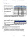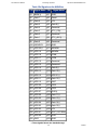
1
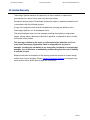
TS-7200 User's Manual
Technologic Systems, Inc.
16610 East Laser Drive, Suite 10
Fountain Hills, AZ 85268
TEL 480.837.5200
FAX 480.837.5300
[email protected]
http://www.embeddedarm.com/
This revision of the TS-7200 manual is dated
Dec. 16, 2004
All modifications from previous versions are listed in Appendix B.
A PDF version of this manual is included on the CD that shipped with your unit(s).
The PDF version includes many active links that may be useful to you.
Copyright © 2004 by Technologic Systems, Inc. All rights reserved.
TS-7200 User's Manual
Technologic Systems
http://embeddedARM.com/
Table of Contents
1 Product Overview..........................................................................................Page 1
1.1 About This Manual.........................................................................Page 1
1.2 Introduction....................................................................................Page 1
1.3 Features and Benefits Summary...................................................Page 2
1.4 Related Products...........................................................................Page 3
2 Memory..........................................................................................................Page 4
2.1 SDRAM..........................................................................................Page 4
2.2 Flash..............................................................................................Page 4
2.3 Compact Flash Cards....................................................................Page 5
2.4 USB Flash Drives...........................................................................Page 6
3 Serial Ports....................................................................................................Page 7
3.1 COM1.............................................................................................Page 7
3.2 COM2.............................................................................................Page 8
3.3 RS-485 Support.............................................................................Page 8
3.4 RS-485 Quick-Start Procedure......................................................Page 9
3.5 Automatic RS-485 TX Enable........................................................Page 10
3.6 Using Automatic RS-485 within Linux...........................................Page 11
3.7 Adding Serial Ports........................................................................Page 11
4 Digital I/O.......................................................................................................Page 13
4.1 DIO Header...................................................................................Page 14
4.2 LCD Header...................................................................................Page 15
4.3 Using DIO Header for SPI bus......................................................Page 16
4.4 LCD Interface................................................................................Page 17
5 A/D Converter................................................................................................Page 18
5.1 Single Sample Acquisition Procedure...........................................Page 19
6 Matrix Keypad Support..................................................................................Page 21
7 Real-Time Clock............................................................................................Page 22
8 10/100 Base-T Ethernet Port.........................................................................Page 23
9 Linux TCP/IP Configuration...........................................................................Page 24
10 Watchdog Timer..........................................................................................Page 25
11 LED, Jumpers and Push-Button Reset.......................................................Page 26
12 PC/104 Bus Expansion...............................................................................Page 27
13 Loading or Transferring Files......................................................................Page 29
13.1 Transferring Files via the Ethernet Port.......................................Page 29
13.2 Transferring Files via Compact Flash..........................................Page 29
13.3 Zmodem Downloads....................................................................Page 30
14 Debugging...................................................................................................Page 31
14.1 Debugging with gdb.....................................................................Page 31
14.2 Low-Level Debugging with RedBoot...........................................Page 32
14.3 Using Other Debuggers...............................................................Page 32
i
12/2004
TS-7200 User's Manual
Technologic Systems
http://embeddedARM.com/
15 Console on TS-7200...................................................................................Page 33
16 Software and Support.................................................................................Page 34
16.1 Linux OS Support........................................................................Page 34
16.2 Other OS Support.......................................................................Page 34
16.3 Development Kit and Supplemental CD.....................................Page 35
17 Installing the TS-7200.................................................................................Page 36
17.1 Electrostatic Discharge (ESD) Precautions................................Page 36
17.2 Setup and Installation Instructions..............................................Page 36
18 Components...............................................................................................Page 37
18.1 Standard Connectors..................................................................Page 37
19 Environmental Specifications.....................................................................Page 38
20 Options and Other Features.......................................................................Page 39
21 Feedback and Updates to the Manual........................................................Page 40
22 Limited Warranty.........................................................................................Page 41
23 FCC Advisory Statement............................................................................Page 42
Appendix A: Product Views.............................................................................Page 43
Appendix B: User Manual Revisions...............................................................Page 44
Appendix C: System Memory Map..................................................................Page 45
Appendix D: Further References.....................................................................Page 46
Appendix E: Schematic....................................................................................Page 47
Contact Information.........................................................................................Page 48
ii
12/2004
TS-7200 User's Manual
Technologic Systems
http://www.embeddedARM.com/
1 Product Overview
1.1 About This Manual
This manual is intended to provide the user with an overview of the board’s features,
benefits, specifications, and set up procedures. It also contains important safety
information.
1.2 Introduction
The model TS-7200 is a compact, full-featured Single Board Computer (SBC) based on
the Cirrus EP9302 ARM9 CPU. The EP9302 features an advanced 200 MHz ARM920T
processor design with a memory management unit (MMU) that allows support for highlevel operating systems such as Linux, Windows CE, and other embedded operating
systems. The ARM920T's 32-bit architecture, with a five-stage pipeline, delivers very
impressive performance at very low power.
The EP9302 CPU has a 16 KB instruction cache and a 16 KB data cache to provide
zero-cycle latency to the current program and data, or they can be locked to guarantee
no-latency access to critical sections of instructions and data. For applications with
instruction-memory size restrictions, the ARM920T’s compressed Thumb instruction set
can be used to provide higher code density and lower Flash storage requirements.
The TS-7200 CPU integer performance at 200 MHz is about twice as fast as the
Technologic Systems 133MHz 586-based products, but costs half as much!
1
12/2004
TS-7200 User's Manual
Technologic Systems
http://www.embeddedARM.com/
1.3 Features and Benefits Summary
The TS-7200 comes standard with these features:
●
●
●
●
●
●
●
●
●
●
●
●
●
●
200 MHz ARM9 CPU with MMU
32MB RAM
8MB on-board Flash (Boots to Linux)
True IDE Compact Flash socket (for additional Flash memory)
10/100 Megabit Ethernet port
2 USB compliant Full Speed host (OHCI) ports -- (12 Mb/s max)
2 COM ports (up to 230 Kbaud)
Watchdog Timer
PC/104 expansion bus
SPI bus interface
20 Digital I/O lines
Alphanumeric LCD and matrix keypad interface
Single +5VDC supply @ 400 mA – (under 2 watts)
Small size -- 3.8 x 4.5 inches (9.7 x 11.5 cm)
These optional features are also available:
●
●
●
●
●
8-channel 12-bit analog-to-digital converter
Battery-backed Real-Time Clock (TS-5620)
RS-485 support on COM2 with automatic TX enable
Temperature sensor
Additional COM ports
TS-7200 power supply:
The TS-7200 requires regulated 5VDC at 400 mA (typical maximum). It is possible to
lower this power significantly by lowering the CPU clock rate or by powering-down the
Ethernet PHY chip.
A quick release screw-down terminal block for the 5V power and power GND
connections is provided for easy connection to an external power supply.
Note:
Supply voltages over 6 VDC may damage the TS-7200.
Be sure to use a regulated 5 VDC power supply, preferably with current limiting to 1 to
3 Amps. A current limited supply is very forgiving of common errors during
development. A PC power supply that may be capable of supplying 20 Amps or more is
not recommended -- it is possible to do irreversible damage to the TS-7200 if the
polarity on the power leads is reversed.
2
12/2004
TS-7200 User's Manual
Technologic Systems
http://www.embeddedARM.com/
When power is first supplied to the TS-7200, the board mounted LEDs are immediately
turned on under hardware control. Once the processor begins execution, the LEDs are
turned off. The RED led is briefly turned on while the processor looks for the TSBOOTROM stored in the first sector of Flash. If the processor does not find the TSBOOTROM, it will turn off the red LED and continuously blink the green LED. If the
LEDs do not turn on at all, the most likely problem is the power supply. Check that the
+5V and GND connections are not reversed. A diode protects the board against
damage in such a situation.
Once the processor has found the TS-BOOTROM, the green LED is turned on just
before jumping to it. The TS-BOOTROM briefly turns off the green, and turns on the
RED, while running the SDRAM initialization and test routines, but otherwise remains
green until RedBoot is called and starts its own initialization. If a problem was detected
with the hardware in the TS-BOOTROM, the LEDs blink alternately red, then green, at a
very fast rate. The red LED is on during RedBoot initialization, and once complete, the
green LED is lit and remains on from that point forward.
1.4 Related Products
Technologic Systems offers an enclosure for the TS-7200. Several daughter boards are
also available that can add functionality via the PC/104 bus. Since the PC/104 bus is an
industry standard, an almost unlimited number of third-party products can be added via
the PC/104 expansion bus.
3
12/2004
TS-7200 User's Manual
Technologic Systems
http://www.embeddedARM.com/
2 Memory
2.1 SDRAM
The TS-7200 uses a 256 Megabit SDRAM chip to provide 32 Megabytes (MB) of highspeed RAM. By using the latest SDRAM technology (a 512 Megabit chip), it is possible
to have 64 MB of RAM on the TS-7200. This option will be available in the near future
when this technology becomes cost-effective.
The TS-7200 SDRAM chip is soldered directly to the board. By not using socketed
memory, the TS-7200 is much more reliable in high-vibration environments.
The TS-7200 RAM is not contiguous in the physical memory map of the EP9302. But
the MMU is programmed to remap the blocks of RAM to appear as a contiguous block
of memory at the very beginning of the virtual memory map. In the case of a 256
Megabit SDRAM chip (32 MB), it is located at 0 through 32 MB in the virtual memory
map.
2.2 Flash
The TS-7200 uses an Intel 3.3V StrataFlash chip for its on-board Flash resource. For
the standard 8 Megabyte chip, this is composed of 64 uniform sectors with 128 Kbytes
per sector. The first sector is reserved for the TS-BOOTROM code. The TS-BOOTROM
code initializes various internal configuration registers for proper operation for the TS7200 design and initializes and tests the SDRAM. The next 48 sectors (6 Mb) are used
for the JFFS2 file system. This is a journaling file system that uses wear leveling at the
file system level to maximize Flash lifetime. It is also extremely tolerant of power failures
during file write sequences. The last 1920Kb are reserved for the RedBoot ROM
monitor, RedBoot FIS (Flash Image System) and RedBoot FCONFIG (Flash config).
The default Linux kernel, vmlinux, is pre-loaded in the FIS and the default boot script
and Ethernet MAC address are contained in the FCONFIG. You may also use the
RedBoot FIS to store and load Flash images that contain eCos applications or other OS/
RTOS bootloaders.
The physical address of the Flash chip is 0x6000_0000 through 0x607F_FFFF for the 8
MB chip. It is possible to use larger sizes of the Intel Strata Flash than the standard
8MB chip. The TS-7200 is designed to accommodate both 16 MB and 32 MB chips.
Please call Technologic Systems to discuss lead times and current costs for these
options.
4
12/2004
TS-7200 User's Manual
Technologic Systems
http://www.embeddedARM.com/
The entire Flash chip can be write-protected by removing Jumper #3. When JP3 is not
installed the Flash chip becomes a read-only resource.
The designer should be aware that Flash technology does have a wear-out mechanism
that should be considered in all designs. The Intel Strata Flash memory is guaranteed
capable of a minimum of 100,000 write/erase cycles. This means that if you completely
erase and rewrite the entire Flash drive 10 times a day, it would take over 27 years
before any problems would occur. Reading the Flash produces no wear at all.
2.3 Compact Flash Cards
If the 6MB Flash file system on the TS-7200 is insufficient for your application,
additional non-volatile storage can be added with a Compact Flash (CF) card. CF cards
can supply additional storage that behaves much as a hard drive does with sizes
ranging from 32MB to 1GB. These products are inherently more rugged than a hard
drive since they are completely solid-state with no moving parts.
The Compact Flash card has the added advantage of being removable media. A
SanDisk USB Compact Flash reader/writer (which is included in the TS-7200
Developer’s Kit) is recommended for the host PC for file transfers. This results in the
ability to quickly move files from a host PC to the TS-7200 using a Compact Flash card
as the removable media. While a USB Compact Flash reader allows for hot swapping of
the Compact Flash card on the host PC, the Compact Flash interface on the TS-7200 is
not hot swappable, the TS-7200 must be rebooted after removing or installing a
Compact Flash card.
The format of the CF card must be in EXT2 format for proper operation with Linux as a
root filesystem.
Note:
The TS-7200 always needs to be powered-off before swapping CF cards.
5
12/2004
TS-7200 User's Manual
Technologic Systems
http://www.embeddedARM.com/
2.4 USB Flash Drives
Additional non-volatile storage can be added with a USB Flash drive. USB Flash drives
can supply additional storage that behaves very much like a CF card except that a CF
card can be the root drive whereas a USB drive can not be the root file system.
The USB Flash drive has the advantage over a CF card in that the USB drive can be
hot swapped.
Note:
Drivers are available in the TS-Linux distribution to support USB Flash Drives.
6
12/2004
TS-7200 User's Manual
Technologic Systems
http://www.embeddedARM.com/
3 Serial Ports
The TS-7200 has two asynchronous serial ports (COM1 and COM2) provide a means to
communicate with external serial devices. Each is independently configured as a
16C550- type COM port that is functionally similar to a standard PC COM port. These
ports have 16-byte FIFOs in both the receive and the transmit UART channels.
Both COM ports can support all standard baud rates up through 230.4Kbaud. Both
COM ports may be configured to use a DMA channel (useful when very high baud rates
are being used).
Either UART can generate:
●
●
four individually-maskable interrupts from the receive, transmit, and modem
status logic blocks
a single, combined interrupt that is asserted if any of the individual interrupts are
asserted and unmasked
COM1 can also the support HDLC protocol -- Download the EP9301 User Guide for
more details.
COM2 can optionally support RS-485 half or full duplex levels.
3.1 COM1
The base address of COM1 appears in the physical
address space at 0x808C_0000.
COM1 has RS-232 support for the following signals:
●
●
●
●
●
●
●
TXD
RXD
RTS
CTS
DTR
DSR
DCD
This full complement of RS-232 signals (all except
Ring Detect) allows COM1 to interface to almost
any serial RS-232 device.
Table 3.1 COM1 DB9 Pin-Outs
DB9 Pin Signal
Description
1
DCD
Data Carrier Detect
2
RXD
Receive Data
3
TXD
Transmit Data
4
DTR
Data Terminal Ready
5
GND
Ground
6
DSR
Data Set Ready
7
RTS
Request to Send
8
CTS
Clear to Send
9
--
--
The COM1 RS-232 port uses a DB-9 male connector on the TS-7200. See Table 3.1 for
a list of COM1 pin-outs.
7
12/2004
TS-7200 User's Manual
Technologic Systems
http://www.embeddedARM.com/
3.2 COM2
The base address of
COM1 appears in the
physical address space
at 0x808D_0000.
Table 3.2 COM2 Serial Port Header Pin-Outs
RS-232
Half Duplex RS-485
9-Pin SubD Signal 9-Pin SubD Signal
1
COM2 has RS-232
support only for the TXD 2
and RXD signals. This is 3
sufficient to interface
4
with serial devices that
5
only require transmit
and receive data lines.
6
COM2 is accessible on
7
a 10-pin header labeled
8
COM2. Adaptor cables
are available to convert 9
these into standard 9pin SubD male connectors.
Full Duplex RS-485
9-Pin SubD
Signal
1
TX+ / RX+ 1
RXD
2
2
TXD
3
3
4
4
RX+
GND
TX+
5
GND
5
GND
6
TX- / RX-
6
TX -
7
7
8
8
9
9
RX -
In addition, COM2 has optional support for full or half-duplex RS-485. See Table 3.2 for
COM2 pin-outs.
Note:
The COM2 serial port 10-pin header has both RS-232 and RS-485 signals. Only one
set is in use for a given application – it is not possible to use both at the same time.
3.3 RS-485 Support
An option is available to add support to COM1 for half duplex or full duplex RS-485. RS485 drivers allow communications between multiple nodes up to 4000 feet (1200
meters) via twisted pair cable. Half-duplex RS-485 requires one twisted pair plus a
Ground connection, while full duplex requires two twisted pair plus a Ground.
8
12/2004
TS-7200 User's Manual
Technologic Systems
http://www.embeddedARM.com/
For half-duplex operation, a single twisted pair is used for transmitting and receiving.
The Auto485.exe utility must be run to initialize the automatic RS-485 control logic. For
full-duplex operation, two twisted pairs are used and the transmit driver is typically
enabled all the time. The auto485.exe utility must be run to put the logic into full-duplex
RS-485 mode.
Fail-safe bias resistors are used to bias the TX+, TX- and RX+, RX- lines to the correct
state when these lines are not being actively driven. This is an important consideration,
since in a typical RS-485 installation, the RS-485 drivers are frequently tri-stated. If failsafe bias resistors are not present, the 485 bus may be floating and very small amounts
of noise can cause spurious characters at the receivers. 4.7KW resistors are used to
pull the TX+ and RX+ signals to 5V and also to bias the TX- and RX- signals to ground.
Termination resistors in many installations are not required when cable lengths are less
than 50 meters and the baud rate is 9600 or less. Termination resistors may be required
for reliable operation when running longer distances or at higher baud rates.
Termination resistors (typically 100-150 ohms) should only be installed at each end of
an RS-485 transmission line. In a multi-drop application where there are several drivers
and/or receivers attached, only the devices at each end of the transmission line pair
should have termination resistors.
A read at I/O location 0x2240_0000 bit 1 will return a "1" when the RS-485 option is
installed.
3.4 RS-485 Quick-Start Procedure
Perform the following steps:
1. Check that the RS-485 option is installed in the TS-7200 (required).
2. Attach the RS-485 cable to the 10-pin header. (Adaptor cables to SubDB9
connector are available from Technologic Systems.)
3. Set the COM2 UART serial parameters (baud rate, data, parity, and stop bits,
interrupts, etc) in your source code
4. Use the TIOC_SBCS485 ioctl() to enable the automatic RS-485 feature.
5. Simply read () and write () data to the COM2 UART – the automatic RS-485 logic
controls TX enable.
9
12/2004
TS-7200 User's Manual
Technologic Systems
http://www.embeddedARM.com/
3.5 Automatic RS-485 TX Enable
Table 3.5 COM2 Mode Register
TS-7200 supports fully automatic
TX enable control under hardware
Value (Hex) MSB MID LSB
Mode
control. This simplifies the design
00
0
0
0
RS-232
of half-duplex systems since
turning off the transmitter and
01
0
0
1
Full-Duplex RS-485
enabling the receiver in software is
02
0
1
0
-- Reserved
typically difficult to implement. If
03
0
1
1
-- Reserved
this is implemented in software,
then the COM2 UART transmit
04
1
0
0
Half-Duplex 9600 baud
holding register and the transmit
05
1
0
1
Half-Duplex 19.2Kbaud
shift register both must be polled
06
1
1
0
Half-Duplex 57.6Kbaud
until empty before deasserting the
07
1
1
1
Half-Duplex 115.2Kbaud
TX enable signal to the RS-485
driver. The design gets more
complicated when using the TX FIFO or when using a multi-tasking OS such as Linux.
The implementation on the TS-7200 uses hardware in a Xilinx PLD to automatically
control when the RS-485 drivers and receivers are selected. The automatic RS-485
logic eliminates the need for any software polling and supervision. A counter in the
Xilinx PLD is used to keep track of the bits shifting out the COM2 UART. This circuit
automatically turns on/off the RS-485 transceiver and receiver at the correct times. This
only requires the COM2 Mode registers in the PLD to be initialized once based on baud
rate and data format.
COM2 will default to RS-232 mode at reset (COM2 mode register = Hex 00). In order to
switch COM2 into Full duplex RS-485 mode, the COM2 Mode register at 0x22C0_0000
must be set to Hex 01. In this mode, the TX drivers are always asserted.
In order to switch COM2 into half-duplex RS-485, then the COM2 mode register at
0x22C0_0000 must be set to Hex 04, 05, 06 or 07 depending upon the baud rate
required. Baud rates of 9600, 19.2K, 57.6K and 115.2K are supported. If you need to
operate COM2 in half-duplex RS-485 at any other baud rate, then contact Technologic
Systems.
A second COM2 Mode register at 0x2300_0000 must be set to Hex 01 if the COM2 is in
half-duplex mode and the data format is using 8 data bits with parity or 8 data bits with 2
stop bits.
Note:
COM2 can support half-duplex RS-485 baud rates of 9600, 19.2K, 57.6K and
115.2Kbaud. For any other baud rate, contact Technologic Systems.
10
12/2004
TS-7200 User's Manual
Technologic Systems
http://www.embeddedARM.com/
3.6 Using Automatic RS-485 within Linux
A special ioctl command has been added to the Linux kernel's serial code to turn off and
on the automatic RS-485 feature. The header files needed to be included from the Linux
kernel source tree and an applications source code are linux/ts_sbc.h and linux/include/
asm/ioctls.h. These header files can be found in a Linux kernel patched with an
appropriate patch from Technologic Systems. The following snippet of code
demonstrates the use of this ioctl.
#include <linux/ts_sbc.h>
#include <linux/include/asm/ioctls.h>
<snip>
mcr = AUTO485FD
//mcr = AUTO485HD //for half duplex
ioctl (fd, TIOC_SBCS485, &mcr);
//write() and read() from fd
ioctl (fd, TIOC_SBCC485, &mcr);
//further reads() and writes() may not behave
3.7 Adding Serial Ports
If your project requires more than two serial ports, additional ports may be added via the
PC/104 expansion bus. Technologic Systems offers three different daughter boards (TSSER1, TS-SER2, and TS-SER4) that add 1, 2, or 4 extra COM ports respectively.
These can be configured using PC designations COM1, COM2, or higher. These will
appear in the TS-7200 PC/104 address space (0x11A0_0000 base address). For
example, a TS-SER1 daughter board can be jumper selected as COM3 which would
correspond to a PC I/O base address of 0x3E8. On the TS-7200, this COM port will
appear at the physical base address of 0x11A0_03E8.
The TS-7200 PC/104 expansion bus has IRQ5, IRQ6, and IRQ7 available for additional
serial port interrupts.
11
12/2004
TS-7200 User's Manual
Technologic Systems
http://www.embeddedARM.com/
Typically each serial port has a dedicated interrupt, but the TS-SER4 daughter board
allows all four extra serial ports to share a single interrupt. This is very helpful in
systems with a large number of serial ports since there are a limited number of IRQ
lines available.
Note:
Drivers are available in the TS-Linux distribution to support these extra COM ports.
12
12/2004
TS-7200 User's Manual
Technologic Systems
http://www.embeddedARM.com/
4 Digital I/O
There are 20 Digital Input/Output (DIO) lines available on the TS-7200. These are
available on two headers labeled “DIO” and “LCD”. The header labeled LCD can be
used as 11 DIO lines or as an alphanumeric LCD interface (See Section 4.2). The
header labeled DIO has 9 DIO pins available. In addition to the DIO signals, each
header also has a power pin and Ground available. The LCD header has 5V power
available while the DIO header has 3.3V power.
Three pins on the DIO header are used to bring out the EP9302 SPI bus. By using
some of the DIO pins as peripheral Chip Select signals, a complete interface is
available for SPI peripherals. It is also possible to bring out a fourth SPI bus function
[SPI_Frame] by adding a 10 ohm resistor in the position labeled R1 on TS-7200 RevB
boards. This signal is not required for many SPI peripherals but it may prove useful in
some applications.
All of the DIO lines are programmable as either inputs or outputs and the direction of
each I/O pin can be individually programmed. All DIO control registers are 8-bits wide
and aligned on word (32-bit) boundaries. For all registers, the upper 24 bits are not
modified when written and are always read back as zeros. Every DIO pin has two
registers used to access it, an 8-bit data register and an 8-bit data direction register
(DDR). The DDR controls whether each DIO pin is an input or an output (”1” = output).
Writing to the data register only affects pins that are configured as outputs. Reading the
data register always returns the state of the DIO pin.
Many of the DIO pins (DIO_0 thru DIO_8 and LCD_0 thru LCD_7) can also be
programmed to cause interrupts. The interrupt properties of these pins are individually
configurable -- each interrupt can be either high or low level sensitive or either rising or
falling edge triggered. It is also possible to enable debouncing on any of these
interrupts. Debouncing is implemented using a 2-bit shift register clocked by a 128 Hz
clock. Download the EP9301 User Manual and see Chapter 21 for details.
The TS-7200 RevB boards also allow access to two 12-bit A/D channels on the DIO
header.
The 5V power output pin on the LCD header has a 750 mA Poly-Fuse to prevent
excessive current. The 3.3V power on the DIO header is current limited to
approximately 1 Amp by an LM1117 3.3V regulator.
13
12/2004
TS-7200 User's Manual
Technologic Systems
http://www.embeddedARM.com/
4.1 DIO Header
The DIO port provides +3.3V, GND, the SPI bus, and 9 digital I/O
lines that may be used to interface the TS-7200 with a wide range
of external devices. DIO lines DIO_0 thru DIO_7 are a byte-wide
port using Port B on the EP9302 and are accessed via the data
register at physical address location 0x8084_0004. The DDR for
this port is at 0x8084_0014.
Table 4.1 DIO Header
Pin-Out
Header Pin Description
1
DIO_0
2
GND
3
DIO_1
4
ADC0
5
DIO_2
6
ADC4 or
SPI_Frame
7
DIO_3
8
DIO_8
Warning!
All pins on the DIO header use 0-3.3V logic levels. Do
not drive these lines to 5V.
9
DIO_4
10
SPI_MISO
11
DIO_5
When the DIO pins are configured as outputs, they can source 4
mA or sink 8 mA and have logic swings between 3.3V and ground.
When configured as inputs, they have standard TTL level
thresholds and must not be driven below 0 Volts or above 3.3
Volts. DIO lines DIO_0 thru DIO_3 have 4.7 KW pull-up resistors
to 3.3V biasing these signals to a logic”1”. The other DIO pins
have 100 KW bias resistors biasing these inputs to a logic “1”.
12
SPI_MOSI
13
DIO_6
14
SPI_CLK
15
DIO_7
16
3.3 V
DIO_8 is accessed via bit 0 of Port F in the EP9302 and is
accessed via the data register at physical address location
0x8084_0030. The DDR for this port is at 0x8084_0034. It is
important not to change the other bit positions in these Port F
registers since these other DIO pins are being used on the TS7200. All accesses to these registers should use read-modify-write
cycles.
DIO signals DIO_0 thru DIO_7 are physically arranged to allow a 16-pin (2x8) ribbon
cable to directly connect a 4x4 matrix keypad. Drivers are available for this interface.
Note:
The SPI interface is described in section 4.3.
A/D Converter
The DIO Port pins 4 and 6 are connected to two of the EP9302 12-bit A/D converter
inputs. These can be used to measure analog signals in the range of 0 to 3.3V.
14
12/2004
TS-7200 User's Manual
Technologic Systems
http://www.embeddedARM.com/
4.2 LCD Header
The LCD Port can be used as 11 additional digital I/O lines or it
can be used to interface to a standard alphanumeric LCD display.
The header has been arranged to allow a 14-pin ribbon cable to
directly connect to industry standard LCD displays. Technologic
Systems has available a 2x24 LCD display with software drivers
for rapid development.
DIO lines LCD_0 thru LCD_7 are a byte-wide port using Port A on
the EP9302 and are accessed via the data register at physical
address location 0x8084_0000. The DDR for this port is at
0x8084_0010.
Since this port is interfacing to a 5V LCD, 1.0 KW resistors have
been added in series between the EP9302 and the LCD_0 thru
LCD_7 pins. This is required since the LCD data bus could be
driving these lines above 3.3V. The series resistors prevent the
LCD from overdriving the EP9302 Port A pins. If using these pins
for general purpose DIO, the current sourcing and sinking
capability of these DIO pins is limited by the 1.0 KW resistors.
Table 4.2 LCD Header
Pin-Out
Header Pin Description
1
5V
2
GND
3
LCD_RS
4
Bias
5
LCD_EN
6
LCD_WR
7
LCD_1
8
LCD_0
9
LCD_3
10
LCD_2
11
LCD_5
12
LCD_4
LCD_EN, LCD_ RS , and LCD_WR are DIO pins using EP9302
LCD_7
Port H bits 3 through 5 respectively and are accessed via the data 13
register at physical address location 0x8084_0040. The DDR for
14
LCD_6
this port is at 0x8084_0044. When these DIO pins are configured
as outputs, they can source 4 mA or sink 8 mA and have logic swings between 3.3V
and ground. When configured as inputs, they have standard TTL level thresholds and
must not be driven below 0 Volts or above 3.3 Volts. These DIO pins have 100 KW bias
resistors biasing these inputs to a logic “1”. It is important not to change the other bit
positions in these Port H registers since the other DIO pins are being used on the TS7200. All accesses to these registers should use read-modify-write cycles.
Warning!
LCD pins 3, 5, and 6 use 0-3.3V logic levels. Do not drive these lines to 5V.
Pin 4 on this header (labeled Bias) is a 620 ohm resistor to ground for LCD contrast
biasing.
The 5V power on the LCD header has a 750 mA Poly-Fuse to limit the current.
15
12/2004
TS-7200 User's Manual
Technologic Systems
http://www.embeddedARM.com/
4.3 Using DIO Header for SPI bus
Table 4.3 DIO Header Pin-Outs
The EP9302 Synchronous Serial
Port is available on the DIO
Header Pin
Name
Function
header. This port can implement
SPI_MISO Master Output /
either a master or slave interface 10
Slave Input
to peripheral devices that have
either Motorola SPI or National
12
SPI_MOSI
Master Output /
Semiconductor Microwire serial
Slave Input
interfaces. The transmit and
receive data paths are buffered
14
SPI_CLK
Clock
with internal FIFO memories
6
SPI_Frame R1 must be added to enable
allowing up to eight 16-bit values
to be stored for both transmit and receive modes. The clock rate is programmable up to
3.7 MHz and has programmable phase and polarity. The data frame size is
programmable from 4 to 16 bits.
By using some of the DIO Header pins as peripheral Chip Select signals, a complete
interface is available for addressing up to 9 SPI peripherals. The SPI bus pins are
defined in the table below.
Warning!
The SPI bus pins use 0-3.3V logic levels. Do not drive these lines to 5V.
Download the EP9301 User’s Manual and see Chapter 19 for more details on using the
SPI bus.
16
12/2004
TS-7200 User's Manual
Technologic Systems
http://www.embeddedARM.com/
4.4 LCD Interface
A 14-pin LCD connector is provided on the
TS-7200 for interfacing with standard
alphanumeric LCD displays. These displays
use a common controller, the Hitachi
HD44780 or equivalent. While software
written for the HD44780 works with all
displays using the controller, the cable
needed is dependent on the display used.
For most displays, a straight-through type
ribbon cable can be used. The connector on
the LCD display is typically mounted on the
backside of the display.
Warning!
Using an incorrect cable or
mounting the LCD connector on the
front-side can result in a reverse
power polarity and can damage the
LCD display. Please refer to your
LCD data sheets for in-depth
information.
Table 4.4a LCD Header Signals
PIN
Function
Comments
1
LCD 5V
LCD Power
2
LCD_GND
3
LCD_RS
Register select
4
Bias
620 Ohm to GND
5
LCD_EN
Active high enable
6
LCD_WR# Active low write
7
LCD_D1
8
LCD_D0
9
LCD_D3
10
LCD_D2
11
LCD_D5
12
LCD_D4
13
LCD_D7
14
LCD_D6
D0 - D7:
Buffered
bi-directional
data bus
Technologic Systems has available a 2x24 LCD display with software drivers for rapid
development.
The pin-outs in the above table are not the standard given for LCD
displays. However, these pin-outs allow a standard ribbon cable to
be used when the ribbon cable is attached to the backside of the
LCD.
Sample code is available for the LCD. Contact Technologic Systems
for more information.
17
Table 4.4b LCD
Header Pin-Outs
2 4 6 8 10 12 14
1 3 5 7 9
11 13
12/2004
TS-7200 User's Manual
Technologic Systems
http://www.embeddedARM.com/
5 A/D Converter
The TS-7200 supports an optional
eight-channel, 12-bit A/D converter
(ADC) with a conversion time of 12
uS. This will allow up to 60,000
samples per second. Each channel
is independently software
programmable for a variety of
analog input ranges: -10V to +10V, 5V to +5V, 0V to +10V, or 0V to
+5V. This allows an effective
dynamic range of 14 bits.
Table 5a A/D Registers
I/O Address
Action
10C0_0000 Write Initiate A/D Conversion
10C0_0000 Read LSB of Conversion
10C0_0001 Read MSB of Conversion
2240_0000 Read
Bit 0 = 1 if A/D option installed
1080_0000 Read
Bit 7 = 0 when Conversion completed
Table 5b A/D Control Register (0x10C0_0000 Write)
Each channel is overvoltage tolerant
from -16V to + 16V, and a fault
Bit
Description
Details
condition on any channel will not
0-2 Analog channel select Channels 0-7
affect the conversion result of the
selected channel. This is all
3
Unipolar / Bipolar
0 = Unipolar (i.e. 0 to +5V)
accomplished with a 5V only power
1 = Bipolar (i.e. -5V to +5V)
supply; no negative supply voltage
is required. The Maxim MAX197
4
Range select
0 = 5V range
chip can be replaced with a
1 = 10V range
MAX199 chip if a lower range of
5-7 Mode bits
Set to 0, 1, 0
analog input levels is required (-4V
to +4V, -2V to +2V, 0V to 4V, and 0V to 2V).
A read at I/O location 0x2240_0000 bit 0 returns a "1" when the A/D option is installed
on the TS-7200.
18
12/2004
TS-7200 User's Manual
Technologic Systems
http://www.embeddedARM.com/
5.1 Single Sample Acquisition Procedure
An acquisition is initiated by writing to I/O location 0x10C0_0000. The
value written to this location determines the channel to convert (bits 0-2)
and selects one of four input ranges (bits 3 and 4). Bits 5, 6, and 7 should
be set to 0, 1, 0 respectively. After the write cycle to location
0x10C0_0000, the MAX197 completes the A/D conversion in about 12
mS. Bit 7 at I/O location 0x2240_0000 may be polled to determine when
the conversion is complete (zero = complete). The conversion result is
now available at locations 0x10C0_0000 (LSB) and 0x10C0_0001
(MSB). A single word read at 0x10C0_0000 can also be used. When
using unipolar modes, the result is in binary format with the upper 4 bits
of the MSB equal to zero. When a bipolar mode is used, the result is in
twos-complement binary with the upper 4 bits (Bits 12-15) equal to bit 11
(sign extended).
Table 5.1a ADC
Header
Pin
Description
1
Channel 0
3
Channel 1
5
Channel 2
7
Channel 3
9
Channel 4
11
Channel 5
13
Channel 6
15
Channel 7
Even Analog GND
If more details on the A/D converter specifications are required,
go to the Maxim web site and search for MAX197.
The following is sample Linux C code for initiating and printing
an ADC conversion on channel 1.
Table 5.1b ADC Header
Pinout
2 4 6 8 10 12 14 16
1 3 5 7 9
11 13 15
#include<unistd.h>
#include<sys/types.h>
#include<sys/mman.h>
#include<stdio.h>
#include<fcntl.h>
#include<assert.h>
int main(int argc, char **argv) {
volatile unsigned short * complete;
volatile unsigned char * lsb, * msb, * control;
int res;
int fd = open("/dev/mem", O_RDWR);
assert(fd != -1);
lsb = control = (unsigned char *)mmap(0, getpagesize(),
19
12/2004
TS-7200 User's Manual
Technologic Systems
http://www.embeddedARM.com/
PROT_READ|PROT_WRITE, MAP_SHARED, fd, 0x10c00000);
msb = lsb + 1;
complete = (unsigned short *)mmap(0, getpagesize(),
PROT_READ|PROT_WRITE, MAP_SHARED, fd, 0x10800000);
// Initiate conversion, channel #1, unipolar, 5V
*control = 0x41;
// Wait for completion
while ((*complete & 0x80) != 0);
// Print result on a scale from 0 to 2^12 - 1
res = *lsb;
res |= *msb << 8;
printf("result: %d\n", res);
close(fd);
return 0;
20
12/2004
TS-7200 User's Manual
Technologic Systems
http://www.embeddedARM.com/
6 Matrix Keypad Support
DIO signals DIO_0 thru DIO_7 are physically arranged to allow a 16-pin (2x8) ribbon
cable to directly connect a 4x4 matrix keypad. Sample code is available for the Matrix
Keypad. Contact Technologic Systems for more information.
21
12/2004
TS-7200 User's Manual
Technologic Systems
http://www.embeddedARM.com/
7 Real-Time Clock
The TS-7200 has an option for a Non-volatile Battery-backed real-time clock (RTC).
This option (TS-5620) is very low-cost daughter board that is only 1.1 x 3.5 inches (2.8 x
9.0 cm) and uses an ST Micro M48T86PC1 module for the real-time clock function. This
module contains the lithium battery, 32.768 kHz crystal, and a RTC chip with 114 bytes
of battery-backed CMOS RAM. It is guaranteed to maintain clock operation for a
minimum of 10 years in the absence of power.
The 114 bytes of non-volatile RAM that is located inside the RTC chip is not reserved
for TS-7200 functionality. This RAM is available for any user functions as required. Call
Technologic Systems for driver support.
The schematic for the TS-5620 is posted on our web site. The TS-5620 design only
uses two chips. This circuitry can be freely used on any customer daughter board
design if the battery-backed RTC feature is necessary.
The RTC is accessed using two registers. The write-only index register is located at
physical address location 0x1080_0000 and the RTC data register is location at
physical address location 0x1170_0000. These are byte-wide registers with the index
register being write only and the data register being read/write. Valid index register
values are between 0 and 127 decimal. The first 14 index locations are used for
accessing the RTC time and date registers.
The next 114 locations are non-volatile RAM locations.
22
12/2004
TS-7200 User's Manual
Technologic Systems
http://www.embeddedARM.com/
8 The 10/100 Base-T Ethernet Port
The EP9302 Ethernet LAN controller incorporates all the logic needed to interface
directly to any MII compatible Ethernet PHY chip. A low-power Micrel KS8721 chip is
used to implement the Ethernet PHY function and an integrated RJ-45 connector with
built-in 10/100 transformer and LED indicators completes the Ethernet sub-system.
The TS-7200 has both a LINK/ACTIVITY LED and a 10/100 speed LED built into each
RJ-45 connector that indicates the current Ethernet status. The LINK LED (left side of
connector, green) is active when a valid Ethernet link is detected. This LED should be
ON whenever the TS-7200 is powered on and properly connected to a 10/100BaseT
Ethernet network. The LINK/ACTIVITY LED will blink to indicate network activity for
either inbound or outbound data. The SPEED LED (right side of connector, amber) will
be on when a 100Mb network is detected and off for a 10Mb network. Both of these
LEDs are controlled by the KS8721 and do not require any overhead by the processor.
The Ethernet PHY chip can be powered down to save about 90 mA of power
consumption. This is controlled by the EP9302 Digital output on Port H bit 2. A logic
zero will power down the KS8721 PHY chip.
23
12/2004
TS-7200 User's Manual
Technologic Systems
http://www.embeddedARM.com/
9 LINUX TCP/IP Configuration
When using the TS-7200 with TS-Linux, the driver for the Ethernet is already compiled
into the kernel.
The TCP/IP settings for the TS-Linux are configured in the file ‘/etc/sysconfig/
ifcfg-eth0’. Below is a listing.
DEVICE=eth0
# Name of Ethernet interface
IPADDR=192.168.0.50
#IP address of this Ethernet interface
NETMASK=255.255.255.0
# Used with NETWORK to determine local IP's
NETWORK=192.168.0.0
#Used with NETMASK to determine local IP's
BROADCAST=192.168.0.255
# broadcast IP for system wide messages
ENABLE=yes
# Initialize on startup
The TCP/IP network settings are configured in the file ‘/etc/sysconfig/
network_cfg’. Below is a listing.
### Technologic Systems
### General Network Configuration File
###
NETWORKING=yes
GATEWAY=192.168.0.1 # Gateway for internet access
GW_DEV=eth0 # Gateway device to use
Hostname="ts7200" # Host name for this computer
BOOTPROTO=static
DEFRAG_IPV4=no
FORWARD_IPV4=no
The TCP/IP name resolution server is configured in the file ‘/etc/resolv.conf’. Below is a
sample.
nameserver 192.168.0.1 # Name server for domain name lookups.
To access the web server, open a web browser and enter 192.168.0.50 as the address.
This displays the sample web page which demonstrates some of the functionality of
Apache with PHP. Use the ifconfig command at the bash prompt to display the status of
the Ethernet ports. See the TS-Linux for ARM support page for more information.
24
12/2004
TS-7200 User's Manual
Technologic Systems
http://www.embeddedARM.com/
10 Watchdog Timer
The TS-7200 implements a watchdog
timer (WDT) unit in the Xilinx PLD. The
WDT can be used to prevent a system
“hanging” due to a software failure. The
WDT causes a full system reset when
the WDT times out, allowing a
guaranteed recovery time from a
software error. To prevent a WDT
timeout, the application must
periodically “feed” the WDT by writing a
specific value to a specific memory
location.
Table 10a Watchdog Timeout Register
Value (Hex) MSB MID LSB
Timeout Period
00
0
0
0
Watchdog Disabled
01
0
0
1
250 mS
02
0
1
0
500 mS
03
0
1
1
1 second
04
1
0
0
-- Reserved
05
1
0
1
2 seconds
06
1
1
0
4 seconds
07
1
1
1
8 seconds
The WDT Control register must be
initialized with the timeout period desired. This may be as short as 250 mS or may be as
high as 8 seconds. After the WDT has been enabled, the WDT counter starts counting.
The application software can reset this counter at any time by “Feeding the WDT”. If the
WDT counter reaches the timeout period, then a full system reset occurs.
Table 10b Watchdog Control Registers
In order to load the WDT Control register,
the WDT must first be “fed”, and then
within 30 uS, the WDT control register
must be written. Writes to this register
without first doing a “WDT feed”, have no
effect.
Register
Address
WDT Control register 0x2380_0000
WDT Feed register
Access
Read/Write
0x23C0_0000 Write Only
In order to clear the WDT counter (feeding the watchdog), a value of 05 must be written
to the WDT Feed register.
Warning!
Do not attempt to use the Watchdog Timer in the EP9302.
When using the Linux OS, the watchdog can be reached from user C code by using the
mmap() system call on the /dev/mem special file to map the areas of physical address
space into process user address space. A user process does not have the physical
address space of the watchdog registers mapped by default.
25
12/2004
TS-7200 User's Manual
Technologic Systems
http://www.embeddedARM.com/
11 LED, Jumpers, and Push-Button Reset
The TS-7200 has two LEDs (one Red and one Green) available for user software.
These LEDs may be used for diagnostics, status messages, and simple output. When
power is first supplied to the TS-7200, both LEDs are immediately turned on under
hardware control. Once the processor begins execution, the LEDs are turned off, then
flashed on and off again briefly. After booting is complete, these LEDs can be used for
user applications.
The status of all jumpers can be read – see the table below.
Table 11 Jumper Listing
Jumper
Function
JP1
Boot to Serial Port COM1 – This is a recovery mechanism that allows the TS-7200 to boot
using COM1 instead of the on-board Flash chip.
JP2
Enable Serial Console – COM1 is used as the Console. (If JP4 is not installed).
JP3
Write Enable Flash – Remove this jumper to write protect the Flash drive.
JP4
Console swapped to COM2 – (requires JP2 installed to enable console).
JP5
Test Jumper – Used to put the TS-7200 into factory-test mode.
JP6
User Jumper –
The Push-Button causes a full-system reset, exactly the same as if the power were
cycled. (See the bootup sequence description on page 6.)
Jumpers 2, 3, 4, and 5 can be read at physical address location 0x1080_0000.
JP2 is bit 0
JP3 is bit 1
JP4 is bit 3
JP5 is bit 4
Logic “1” = Jumper ON
Logic “1” = Jumper ON
Logic “0” = Jumper ON
Logic “0” = Jumper ON
Jumper 6 can be read at physical address location 0x2280_0000. When bit 0 is a 1, JP6
is on.
The RED and Green LEDs can be controlled at physical address location 0x8084_0020.
Bit 1 is the RED LED and bit 0 is the Green LED. A Logic “1” turns the LED on.
26
12/2004
TS-7200 User's Manual
Technologic Systems
http://www.embeddedARM.com/
12 PC/104 Bus Expansion
Table 12a PC/104 Memory Map
The PC/104 is a compact
implementation of the PC/AT ISA bus
Physical Address Region Emulates x86 cycle
ideal for embedded applications.
Designers benefit from using an already- 11E0_0000 thru 11E0_03FF 8-bit I/O cycles
developed standard, rather than creating 21E0_0000 thru 21E0_03FE 16-bit I/O cycles
their own. Further, the presence of a
11A0_0000 thru 11AF_FFFF 8-bit Memory cycles
compact form-factor PC compatible
21A0_0000 thru 21AF_FFFE 16-bit Memory cycles
standard has encouraged the
development of a broad array of off-the-shelf products, allowing a very quick time to
market for new products.
The electrical specification for the PC/104 expansion bus is identical to the PC ISA bus.
The mechanical specification allows for the very compact implementation of the ISA bus
tailor made for embedded systems. The full PC/104 specification is available from the
IEEE Standards Office under # IEEE P996.1 (see Appendix D for further information).
Basically, this bus allows multiple daughter boards in a 3.6 inch by 3.8 inch form factor
to be added in a self-stacking bus. Since the electrical specs are identical (except for
drive levels) to a standard PC ISA bus, standard peripherals such as COM ports, Digital
I/O, Ethernet ports, and LCD drivers may be easily added.
The TS-7200 implements a sub-set of the full PC/104 bus. This allows the support of
many common I/O daughter boards. Some of the PC/104 signals are not supported
such as the DMA signals. These pins are used on the TS-7200 to support data lines D8D15. This means that a full 16-bit data bus implementation of the PC/104 bus is
possible by only using the 64-pin connector. The supplemental 40-pin connector is only
required for legacy boards – any new design can implement a full 16-bit data bus with
only the 64-pin connector.
PC/104 peripherals will appear in the TS-7200 physical address space in one of four
address regions depending upon whether it is emulating an x86 Memory cycle or I/O
cycle and whether it needs to be a 8-bit cycle or a 16-bit cycle. Each region is a full 1MB
in size, even though the I/O region will typically only use a 1 Kbyte region for legacy
products.
I/O cycles on the PC/104 expansion bus strobe either IOR# or IOW#, while Memory
cycles strobe the MEMR# or MEMW# signals.
For example, a TS-SER1 daughter board can be jumper-selected as COM3, which
would correspond to a PC I/O base address of 0x3E8. Since this is an 8-bit peripheral,
this COM port must be accessed at the physical base address of 0x11A0_03E8.
27
12/2004
TS-7200 User's Manual
Technologic Systems
http://www.embeddedARM.com/
Table 12b Signals on the 8-Bit Bus
PIN Signal Name PIN
Signal Name
A1
BHE# †
B1
GND
A2
Data 7
B2
Reset
A3
Data 6
B3
+5V
A4
Data 5
B4
Data 8 †
A5
Data 4
B5
Reserved
A6
Data 3
B6
RTC_CS †
A7
Data 2
B7
Reserved
A8
Data 1
B8
RTC_ALE †
A9
Data 0
B9
Reserved
A10 IOCHRDY
B10 GND
A11 ADD 20 †
B11 MEMW#
A12 ADD 19
B12 MEMR#
A13 ADD 18
B13 IOW#
A14 ADD 17
B14 IOR#
A15 ADD 16
B15 Reserved
A16 ADD 15
B16 Reserved
A17 ADD 14
B17 Data 9 †
A18 ADD 13
B18 Data 10 †
A19 ADD 12
B19 ADD 21 †
A20 ADD 11
B20 Data 12 †
A21 ADD 10
B21 IRQ7
A22 ADD 09
B22 IRQ6
A23 ADD 08
B23 IRQ5
A24 ADD 07
B24 GND †
A25 ADD 06
B25 Data 11 †
A26 ADD 05
B26 Data 13 †
A27 ADD 04
B27 Data 14 †
A28 ADD 03
B28 Data 15 †
A29 ADD 02
B29 +5V
A30 ADD 01
B30 OSC (14.3 MHz)
A31 ADD 00
B31 GND
A32 GND
B32 GND
† These signals have a non-standard usage.
28
12/2004
TS-7200 User's Manual
Technologic Systems
http://www.embeddedARM.com/
13 Loading or Transferring Files
Three methods are available for transferring files between a desktop PC and your TS7200: Compact Flash, Ethernet downloads, and Zmodem downloads. Full descriptions
of each are detailed below. Other programs that use serial ports to transfer should work
as well.
13.1 Transferring files via the Ethernet port
The default JFFS2 Linux root file system includes a small FTP server that can be used
for uploading/downloading of files across an Ethernet network. Simply point your
preferred FTP client to your TS-7200 IP address (default is 192.168.0.50). You can
login as root or any valid user previously created from the useradd utility. By default, the
JFFS2 image will not accept anonymous FTP.
13.2 Transferring files via Compact Flash
The TS-7200 removable Compact Flash card can be used to easily move files from a
host system. We suggest using a low-cost SanDisk USB Compact Flash card interface
for your host system. This is included in the TS-7200 Developer’s Kit.
For best results, we have noticed that it is best to boot the host PC with a Compact
Flash card installed in the SanDisk USB Reader. The Compact Flash card can then be
hot swapped (inserted or removed without rebooting the host PC).
There are two other options for connecting a Compact Flash to your host computer. A
Compact Flash to PCMCIA adapter, which can map a Compact Flash as a hard drive
on your laptop host computer. Or, a Compact Flash to IDE adapter, which connects to
the 40 pin IDE interface on you host computer. The IDE adapter will allow you can boot
to CF, run fdisk, format, etc.
29
12/2004
TS-7200 User's Manual
Technologic Systems
http://www.embeddedARM.com/
13.3 Zmodem Downloads
Using the Zmodem protocol to send files to and from the TS-7200 is simple and
straightforward. The only requirement is a terminal emulation program that supports
Zmodem, and virtually all do. If you are using Windows 95 or later for your development
work, the HyperTerminal accessory works well.
To download a file to the TS-7200 from your host PC, execute rz at the Linux command
line on the TS-7200 (while using console-redirection from within your terminal emulator)
and begin the transfer with your terminal emulator. In HyperTerminal, this is 'Send
File...' from the 'Transfer' menu.
To upload a file from the TS-7200 to your host PC, execute sz <FILENAME> at the
Linux command line on the TS-7200 and start the transfer in your terminal emulator.
Many emulators, HyperTerminal among them, will automatically begin the transfer
themselves.
Occasionally there may be errors in transmission due to background operations. This is
not a problem -- Zmodem uses very accurate CRC checks to detect errors and simply
resends bad data. Once the file transfer is complete the file is completely error free.
For best results when using HyperTerminal, the hardware handshaking must be
enabled in HyperTerminal.
30
12/2004
TS-7200 User's Manual
Technologic Systems
http://www.embeddedARM.com/
14 Debugging
There are two main methods for debugging on the TS-7200: Debugging from a running
Linux OS with gdb, or from RedBoot (before the Linux kernel is executed)
14.1 Debugging with gdb
The GNU debugger is a sophisticated open source debugger. It can be used with java,
c, c++, or even Fortran. Please see the GNU Debugger Documentation homepage for
more information. The following quickly walks through debugging a sample helloworld
application. The source code in this example is:
int squareit(int n)
{
int x;
x = n * n;
return x;
}
main ( )
{
int i;
for (i = 0; i < 4; i++)
{
printf("number %d\t", i);
printf("number squared: %d\n", squareit(i));
}
return 0;
};
Boot to the CF card, login as root
apt-get install vim (for a text editor)
apt-get install gdb (ensure that the debugger is installed)
Write the above source code into helloworld.c
gcc -g -o hello helloworld.c (compile the source with debugging symbols)
gdb ./hello
(gdb) list 1 (shows the source code)
(gdb) break 6 (sets a breakpoint at line number 6... this line would be return x; from
the squareit function)
31
12/2004
TS-7200 User's Manual
Technologic Systems
http://www.embeddedARM.com/
(gdb) run (start the program)
(gdb) c (continue past the break point)
(gdb) set x=0 (this time, the return value is set to 0 instead of 1)
(gdb) c (continue and you'll see displayed on the screen “number 1 number squared
0”)
quit (exit gdb)
14.2 Low Level Debugging with RedBoot
To provide simple, direct access to the TS-7200 hardware, RedBoot has an integrated
debugger that can perform standard low-level debugger functions. It can be used to
view or set values in memory using the dump and memfill commands. For example, the
command
dump -b 0x80840020
shows that the first byte is filled with zeros, indicating that both the green and red led
are turned off. the -b refers to a location in memory to display.
mfill -b 0x80840020 -p 0x03 -l 0x04
will result in the both the green and red LEDs being turned on. The -b, again, refers to a
location in memory. The -p indicates the pattern to write into memory, and the -l refers
to the length of the data being written out.
To verify that the write was successful,
dump -b 0x80840020
shows the first byte being having a value of 0x03 (bits 0 and 1 being set).
14.3 Using Other Debuggers
Other Linux-capable debuggers will work with the TS-7200. Please refer to your
debugger's manual for both installation and use.
32
12/2004
TS-7200 User's Manual
Technologic Systems
http://www.embeddedARM.com/
15 Console on the TS-7200
The TS-7200 has no video controller or keyboard interface. This was done to keep the
board size small and the cost low. COM1 is typically used as a console port to interface
the TS-7200 to a standard terminal emulation program on a Host PC.
Simply connect an ANSI terminal (or emulator) to COM1 using a null modem cable (this
is included in the TS-7200 Development Kit), using serial parameters of 115,200 baud,
8 data bits, no parity, 1 stop bit, and make sure jumper JP2 is installed.
The console can be changed to COM2 by installing JP4 (with JP2 also installed).
If your application does not require a console or both COM ports are required, then
removing the jumper JP2 easily disables all console output.
33
12/2004
TS-7200 User's Manual
Technologic Systems
http://www.embeddedARM.com/
16 Software and Support
●
●
●
●
Free system software and documentation updates available on our web site
Free technical support by phone, fax, or email
30-day, money back guarantee on evaluation units
One-year, full warranty
16.1 Linux OS Support
The TS-7200 is shipped standard with the Linux OS using Version 2.4.26 kernel. 2MB
of the on-board Flash is reserved for the Linux boot loader and the Linux kernel, with
the remaining 6MB of Flash formatted as a 6 MB JFFS2 file system. The root file
system can be any of the following:
●
●
●
6MB JFFS2 file system image in the on-board Flash (RedBoot should include the
option root=/dev/mtdblock1 to instruct the kernel to boot here)
Compact Flash card (RedBoot should include the option root=/dev/hda)
NFS root (via Ethernet port) (RedBoot should include relevant kernel command
line options: e.g. root=/dev/nfs nfsroot=192.168.0.11:/u/nfsroot ip=dhcp
16.2 Other OS Support
The TS-7200 can be loaded with other operating systems such as Windows CE,
NetBSD, etc. Technologic Systems will provide support for these, and possibly other
operating systems, in the near future. Currently, only Linux and NetBSD are supported
on the TS-7200.
34
12/2004
TS-7200 User's Manual
Technologic Systems
http://www.embeddedARM.com/
16.3 Development Kit and Supplemental CD
The development kit contains a 256Mb Compact Flash that includes a self-hosting ARM
installation of the Debian 2.0 distribution compiled for ARM complete with toolchain.
The supplemental CD contains:
●
●
●
●
●
Fully preinstalled Debian Tarball (for use as an NFS root or on a very large
Compact Flash)
Cross GCC toolchain
Prepatched kernel source code
Prepatched ECOS/RedBoot source code
Supporting documentation
35
12/2004
TS-7200 User's Manual
Technologic Systems
http://www.embeddedARM.com/
17 Installing the TS-7200
17.1 Electrostatic Discharge (ESD) Precautions
Before performing any set up or placement procedures, take the precautions outlined in
this section. Be sure to take appropriate Electrostatic Discharge (ESD) precautions.
Disconnect the power source before moving, cabling, or performing any set up
procedures.
17.2 Setup and Installation Instructions
Follow these guidelines for safety and maximum product performance:
●
Observe local health and safety requirements and guidelines for manual material
handling.
Setup Tools
Depending on placement and cabling, you may need the following tools:
●
●
Small flat-blade screwdriver
Small Phillips screwdriver
Setup Procedure
After locating, setting up, grounding, and cabling the TS-7200,
●
●
Apply power.
Monitor the TS-7200 using a terminal emulator to verify that the board is
operating properly.
Disconnecting AC Power
●
●
Unplug from the power source.
Disconnect other cables as required.
36
12/2004
TS-7200 User's Manual
Technologic Systems
http://www.embeddedARM.com/
18 Components
18.1 Standard Connectors
See Appendix A for other views.
TS-7200 Single-Board ARM shown with optional IDE Compact Flash A/D and RS-485
37
12/2004
TS-7200 User's Manual
Technologic Systems
http://www.embeddedARM.com/
19 Environmental Specifications
To ensure optimum product operation you must maintain the operational environmental
specifications listed in the table below.
Environmental
Specifications
Ambient
Temperature
Relative Humidity
Standard Temp Products
0 to 70° C
The internal
temperature
must not exceed
+70° C.
Extended Temp Products
Extended temperature
range is optional
Note: Refer to your
product manual, or
contact Technologic
Systems if the
environmental
temperature of the
location is in doubt.
0 to 90%
relative humidity
Not to exceed 90% noncondensing.
Not to exceed 90%
noncondensing
38
12/2004
TS-7200 User's Manual
Technologic Systems
http://www.embeddedARM.com/
20 Options and Other Features
●
●
RS-485 is optional
A wall-mounted power supply is available for this product
39
12/2004
TS-7200 User's Manual
Technologic Systems
http://www.embeddedARM.com/
21 Feedback and Updates to the Manual
To help our customers make the most of our products, we are continually making
additional and updated resources available on the Technologic Systems web site.
These include manuals, application notes, programming examples, and updated
software and firmware. Check in periodically to see what's new!
When we are prioritizing work on these updated resources, feedback from customers
(and prospective customers) is the number one influence. If you have questions,
comments, or concerns about your TS-7200 Embedded PC, please let us know.
40
12/2004
TS-7200 User's Manual
Technologic Systems
http://www.embeddedARM.com/
22 Limited Warranty
Technologic Systems warrants this product to be free of defects in material and
workmanship for a period of one year from date of purchase.
During this warranty period Technologic Systems will repair or replace the defective unit
in accordance with the following process:
A copy of the original invoice must be included when returning the defective unit to
Technologic Systems, Inc. at the address below.
This limited warranty does not cover damages resulting from lighting or other power
surges, misuse, abuse, abnormal conditions of operation, or attempts to alter or modify
the function of the product.
This warranty is limited to the repair or replacement of the defective unit. In no
event shall Technologic Systems be liable or responsible for any loss or
damages, including but not limited to any lost profits, incidental or consequential
damages, loss of business, or anticipatory profits arising from the use or inability
to use this product.
Repairs made after the expiration of the warranty period are subject to a repair charge
and the cost of return shipping. Please contact Technologic Systems to arrange for any
repair service and to obtain repair charge cost information.
41
12/2004
TS-7200 User's Manual
Technologic Systems
http://www.embeddedARM.com/
23 FCC Advisory Statement
Warning!
This equipment generates, uses, and can radiate radio frequency energy and if not
installed and used properly (that is, in strict accordance with the manufacturer’s
instructions), may cause interference to radio and television reception. It has been type
tested and found to comply with the limits for a Class A computing device in accordance
with the specifications in Subpart J of Part 15 of FCC Rules, which are designed to
provide reasonable protection against such interference when operated in a commercial
environment. Operation of this equipment in a residential area is likely to cause
interference, in which case the owner at his own expense will be required to correct the
interference.
If this equipment does cause interference, which can be determined by turning the unit
on and off, the user is encouraged to try the following measures to correct the
interference:
●
●
●
●
●
Reorient the receiving antenna.
Relocate the unit with respect to the receiver.
Plug the unit into a different outlet so that the unit and receiver are on different
branch circuits.
Ensure that mounting screws and connector attachment screws are tightly
secured.
Ensure that good quality, shielded, and grounded cables are used for all data
communications.
If necessary, the user should consult the dealer or an experienced radio/television
technician for additional suggestions. The following booklets prepared by the Federal
Communications Commission (FCC) may also prove helpful:
How to Identify and Resolve Radio-TV Interference Problems (Stock No. 004-000000345-4)
Interface Handbook (Stock No. 004-000-004505-7)
These booklets may be purchased from the Superintendent of Documents, U.S.
Government Printing Office, Washington, DC 20402
42
12/2004
TS-7200 User's Manual
Technologic Systems
http://www.embeddedARM.com/
Appendix A: Product Views
Download the mechanical drawing PDF file
43
12/2004
TS-7200 User's Manual
Technologic Systems
http://www.embeddedARM.com/
Appendix B: User Manual Revisions
Date of Issue/Revision
Revision Number
Comments
August 2004
1.0
Initial release
August 26, 2004
Preliminary DRAFT
PRELIMINARY release for first customer ship
December 16, 2004
1.1
Overall clean-up
44
12/2004
TS-7200 User's Manual
Technologic Systems
http://www.embeddedARM.com/
Appendix C: System Memory Map
Sorry...
The TS-7200 Memory Map is not finished yet. Please contact one of our engineers and
we will gladly go over the details with you.
45
12/2004
TS-7200 User's Manual
Technologic Systems
http://www.embeddedARM.com/
Appendix D: Further References
Download the EP9302 Data Sheet PDF file
46
12/2004
TS-7200 User's Manual
Technologic Systems
http://www.embeddedARM.com/
Appendix E: Schematic
Download the TS-7200 Schematic PDF file
47
12/2004
TS-7200 User's Manual
Technologic Systems
http://www.embeddedARM.com/
Contact Information
Technologic Systems
http://www.embeddedARM.com
16610 East Laser Drive, Suite 10
Fountain Hills, AZ 85268
TEL 480.837.5200
FAX 480.837.5300
email: [email protected]
48
12/2004