1
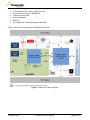
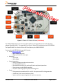
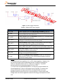
FRDM-KL25Z User Manual Rev. 0 Freescale Semiconductor Inc. FRDMKL25ZUM Table of Contents Overview ..................................................................................................................................................... 3 Reference Documents................................................................................................................................. 3 Getting Started............................................................................................................................................ 3 FRDM-KL25Z Hardware Overview .............................................................................................................. 3 FRDM-KL25Z Hardware Description ........................................................................................................... 6 Power Supply .......................................................................................................................................... 6 Serial and Debug Adapter (OpenSDA) .................................................................................................... 8 Bootloader Mode ............................................................................................................................................................... 8 Application Mode ............................................................................................................................................................... 8 Debug Application .............................................................................................................................................................. 8 MSD Application ................................................................................................................................................................. 8 KL25Z Microcontroller ............................................................................................................................ 8 Clock Source ....................................................................................................................................................................... 8 USB Interface ...................................................................................................................................................................... 8 Reset................................................................................................................................................................................... 8 Debug ................................................................................................................................................................................. 8 Capacitive Touch Slider ........................................................................................................................... 8 3-axis Accelerometer .............................................................................................................................. 9 RGB LED ................................................................................................................................................... 9 Input/Output Headers ............................................................................................................................ 9 Arduino Compatibility ............................................................................................................................. 9 List of Figures Figure 1. FRDM-KL25Z Block Diagram ........................................................................................................ 4 Figure 2. FRDM-KL25Z Feature Call-outs (Preliminary) ............................................................................. 5 Figure 3. Power Supply Schematic.............................................................................................................. 7 Revision History Revision 0 FRDMKL25ZUM Date Changes FRDM-KL25Z User Manual Page 2 of 10 Overview The Freescale Freedom development platform is an evaluation and development tool ideal for rapid prototyping of microcontroller-based applications. The hardware design is form-factor compatible with popular third-party hardware designed to work with Arduino™ and Arduino-compatible boards. The Freescale Freedom KL25Z hardware is a simple, yet sophisticated design featuring a Kinetis L Series microcontroller, the industry’s first microcontroller built on the ARM® Cortex™-M0+ core. The KL25Z128VLK4 is the featured microcontroller on the FRDM-KL25Z. This KL2 family device boasts an energy-efficient core and system platform with a max operating frequency of 48MHz, 128KB of flash, a full-speed USB controller, and loads of analog and digital peripherals. The specifications of the KL25Z128 and the flexible design of the FRDM-KL25Z enable a wide variety of design prototypes including those dependent on battery power or harvested energy. The FRDM-KL25Z is the first hardware platform to feature the Freescale open standard embedded serial and debug adapter known as OpenSDA. This circuit offers the user several options for serial communications, flash programming and run-control debugging. There are also many software development tool options available to the user. Choices include CodeWarrior for Microcontrollers, IAR Embedded Workbench, Keil MDK featuring the µVision IDE, Red Suite from Code Red Technologies, Atollic TrueSTUDIO, Rowley Crossworks, and more. All of these features combine to give the user the freedoms needed to rapidly prototype many embedded designs: a powerful microcontroller built on a very low-power core and SoC platform, easyaccess to I/O with a large ecosystem of compatible hardware, a flexible programming and debug interface, and a large ecosystem of software development environments. Freedom! Reference Documents FREEDOM-KL25Z Pinouts.xlsx OpenSDA User’s Guide - Spreadsheet of all microcontroller and I/O header pin connections. - A guide for users of the OpenSDA embedded circuit. Getting Started FRDM-KL25Z Hardware Overview The FRDM-KL25Z hardware is a Freescale Freedom development platform microcontroller board assembly with the following features: Kinetis L Series KL2 family MCU in an 80 LQFP package FRDMKL25ZUM FRDM-KL25Z User Manual Page 3 of 10 I/O headers for easy access to MCU I/O pins Freescale inertial sensor, MMA8451Q Capacitive touch slider Reset pushbutton RGB LED On-board serial and debug adapter (OpenSDA) Figure 1 shows a block diagram of the FRDM-KL25Z design. Figure 1. FRDM-KL25Z Block Diagram FRDMKL25ZUM FRDM-KL25Z User Manual Page 4 of 10 Figure 2. FRDM-KL25Z Feature Call-outs (Preliminary) The FRDM-KL25Z features two microcontrollers (MCUs): the target MCU and a serial and debug adapter (OpenSDA) MCU. The target MCU is a Kinetis L Series KL2 family device, the KL25Z128VLK4. The OpenSDA MCU is a Kientis K Series K20 family device, the K20DX128VFM5. Features of the KL25Z128VLK4 target MCU include: 32-bit ARM Cortex-M0+ core - up to 48 MHz operation - Single-cycle fast I/O access port Memories - 12 KB flash - 16 KB SRAM System integration - Power management and mode controllers - Low-leakage wakeup unit - Bit manipulation engine for read-modify-write peripheral operations - Direct memory access (DMA) controller - Computer operating properly (COP) Watchdog timer Clocks - Clock generation module with FLL and PLL for system and CPU clock generation - 4 MHz and 32 kHz internal reference clock - System oscillator supporting external crystal or resonator FRDMKL25ZUM FRDM-KL25Z User Manual Page 5 of 10 - Low-power 1kHz RC oscillator for RTC and COP watchdog Analog peripherals - 16-bit SAR ADC w/ DMA support - 12-bit DAC w/ DMA support - High speed comparator Communication peripherals - Two 8-bit Serial Peripheral Interfaces (SPI) - USB dual-role controller with built-in FS/LS transceiver - USB voltage regulator - Two I2C modules - One low-power UART and two standard UART modules Timers - One 6-channel Timer/PWM module - Two 2-channel Timer/PWM modules - 2-channel Periodic Interrupt Timer (PIT) - Real time clock (RTC) - Low-power Timer (LPT) - System tick timer Human-Machine Interfaces (HMI) - General purpose input/output controller - Capacitive touch sense input interface hardware module FRDM-KL25Z Hardware Description Power Supply The FRDM-KL25Z offers a design with multiple power supply options. It can be powered from either of the USB connectors, the VIN pin on the I/O header, an on-board coin cell battery, or an off-board 1.713.6V supply from the 3.3V pin on the I/O header. The USB and VIN supplies are regulated on-board using a 3.3V linear regulator to produce the main power supply. The other two sources are not regulated on-board. Table 1 provides the operational details and requirements for the power supplies. Table 1. Power Supply Requirements Supply Source Valid Range OpenSDA USB (J7) KL25Z USB (J5) VIN Pin 3.3V Pin Coin Cell Battery 5V 5V 4.3-9V 1.71-3.6V 1.71-3.6V OpenSDA Operational? Yes No No No No Regulated onboard? Yes Yes Yes No No Note that the OpenSDA circuit is only operational when a USB cable is connected and supplying power to J7. However, protection circuitry is in place to allow multiple sources to be powered at once. Figure 3 shows the schematic drawing for the power supply inputs and the on-board voltage regulator. FRDMKL25ZUM FRDM-KL25Z User Manual Page 6 of 10 Figure 3. Power Supply Schematic Table 2. FRDM-KL25Z Power Supplies Power Supply Name P5-9V_VIN P5V_SDA P5V_KL25Z P3V3_VREG P3V3_BATT P3V3 P3V3_KL25Z P3V3_SDA P5V_USB Description Power supplied from the VIN pin of the I/O headers (J9 pin 16). Power supplied from the OpenSDA USB connector (J7). A Schottky diode provides back drive protection. Power supplied from the KL25Z USB connector (J5). A Schottky diode provides back drive protection. Regulated 3.3V supply. Sources power to the P3V3 supply rail through a back drive protection Schottky diode. 1 Coin cell battery supply voltage. Sources power to the P3V3 supply rail through a back drive protection Schottky diode. Main supply rail for the FRDM-KL25Z assembly. May be sourced from P3V3_VREG, P3V3_BATT, or directly from the I/O headers (J9 pin 8) KL25Z MCU supply. Header J4 provides a convenient means for energy consumption measurements. 2 OpenSDA circuit supply. Header J3 provides a convenient means for energy consumption measurements. 2 Nominal 5V supplied to the I/O headers (J9 pin 10). Sourced from either the P5V_KL25Z or P5V_OSDA supply through a back drive protection Schottky diode. Notes: 1) By default the linear regulator, U1, is a 3.3V output regulator. However, this is a common footprint that would allow the user to modify the assembly to utilize an alternative device such as a 1.8V or 2.5V regulator. The KL25Z microcontroller has an operating range of 1.71V to 3.6V. 2) J3 and J4 are not populated by default. The two pins of these headers are shorted together by a trace on the bottom layer of the PCB. To measure the energy consumption of either the KL25Z or the OpenSDA MCU, the trace between these pins must first be cut. A current probe or a shunt resistor and voltage meter can then be applied to measure the energy consumption on these rails. FRDMKL25ZUM FRDM-KL25Z User Manual Page 7 of 10 <<To do: Add J9 power supply information. Include details on how power can be sourced and the IOREF pin >> Serial and Debug Adapter (OpenSDA) <<To Do: add details and diagrams here>> Bootloader Mode How to enter bootloader mode Application Mode Debug Application MSD Application KL25Z Microcontroller Clock Source The Kinetis KL2 microcontrollers feature an on-chip oscillator compatible with three ranges of input crystal or resonator frequencies: 32-40 kHz (low freq. mode), 3-8 MHz (high freq. mode, low range) and 8-32 MHz (high freq. mode, high range). The KL25Z128 on the FRDM-KL25Z is clocked from an 8 MHz crystal. <<To Do: add note about RTC_CLKIN pin and use cases>> USB Interface The Kinetis KL2 microcontrollers feature a dual-role USB controller with on-chip full-speed and lowspeed transceivers. The USB interface on the FRDM-KL25Z is configured as a full-speed USB device. J5 is the USB connector for this interface. Reset The PTA20/RESET signal on the KL25Z128 is connected externally to a pushbutton, SW1, and also to the OpenSDA circuit. The reset button can be used to force an external reset event in the target MCU. The reset button can also be used to force the OpenSDA circuit into bootloader mode. Please refer to the Serial and Debug Adapter (OpenSDA) section for more details. Debug The sole debug interface on all Kinetis L Series devices is a Serial Wire Debug (SWD) port. The primary controller of this interface on the FRDM-KL25Z is the onboard OpenSDA circuit. However, an unpopulated 10-pin (0.05”) Cortex Debug connector, J6, provides access to the SWD signals. Capacitive Touch Slider Two Touch Sense Input (TSI) signals, TSI0_CH9 and TSI0_CH10, are connected to capacitive electrodes configured as a touch slider. <<To Do: add a diagram highlighting which electrode is CH9 and which is CH10>> FRDMKL25ZUM FRDM-KL25Z User Manual Page 8 of 10 3-axis Accelerometer A Freescale MMA8451Q low-power, three-axis accelerometer is interfaced through an I2C bus and two GPIO signals as shown in Table 3 below. By default, the I2C address is 0x1D (SA0 pulled high). Table 3. Accelerometer Signal Connections MMA8451Q SCL SDA INT1 INT2 KL25Z128 PTE24 PTE25 PTA14 PTA15 RGB LED Three PWM-capable KL25Z128 signals are connected to a red, green, blue LED. The signal connections are shown in Table 4 below. Table 4. RGB LED Signal Connections RGB LED Red Cathode Green Cathode Blue Cathode KL25Z128 PTB18 PTB19 PTD1 1 Notes: 1) PTD1 (also known as D13) is also connected to the I/O header on J2 pin 10. Input/Output Headers The KL25Z128VLK4 microcontroller is packaged in an 80-pin LQFP. Some pins are utilized in on-board circuitry, but many are directly connected to one of four I/O headers. The pins on the KL25Z microcontroller are named for their general purpose input/output port pin function. For example, the 1st pin on Port A is referred to as PTA1. The I/O connector pin names are given the same name as the KL25Z pin connected to it, where applicable. <<To Do: Diagram of IO headers w/ pin names overlaid>> Note that all pinout data is available in spreadsheet format. See the Reference Documents section for details. <<To Do: Format tables of I/O header data as an appendix. Sort by KL25Z pin #, pin name, and header pin number>> Arduino Compatibility The I/O headers on the FRDM-KL25Z are arranged to allow compatibility with peripheral boards (know as shields) that connect to Arduino and Arduino-compatible microcontroller boards. The outer rows of pins (the even numbered pins) on the headers share the same mechanical spacing and placement as the I/O headers on the Arduino Uno Revision 3 board design. FRDMKL25ZUM FRDM-KL25Z User Manual Page 9 of 10 <<To Do: add note about 3.3V vs. 5V systems and IOREF pin >> FRDMKL25ZUM FRDM-KL25Z User Manual Page 10 of 10