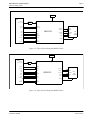
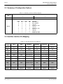
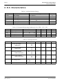
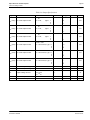
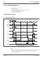
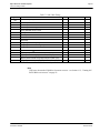
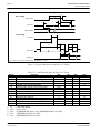
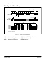
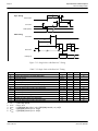
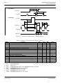
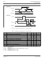
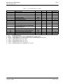
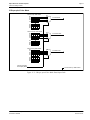
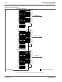
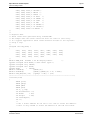
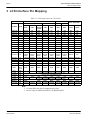
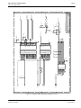
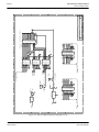
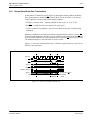
1
SED1375 Embedded Memory LCD Controller SED1375 TECHNICAL MANUAL Document No. X27A-Q-001-01 Copyright © 1999 Epson Research and Development, Inc. All Rights Reserved. Information in this document is subject to change without notice. You may download and use this document, but only for your own use in evaluating Seiko Epson/EPSON products. You may not modify the document. Epson Research and Development, Inc. disclaims any representation that the contents of this document are accurate or current. The Programs/Technologies described in this document may contain material protected under U.S. and/or International Patent laws. EPSON is a registered trademark of Seiko Epson Corporation. All other Trademarks are the property of their respective owners Page 2 Epson Research and Development Vancouver Design Center THIS PAGE LEFT BLANK SED1375 X27A-Q-001-01 TECHNICAL MANUAL Issue Date: 99/03/04 Epson Research and Development Vancouver Design Center Page 3 Customer Support Information Comprehensive Support Tools Seiko Epson Corp. provides to the system designer and computer OEM manufacturer a complete set of resources and tools for the development of graphics systems. Evaluation / Demonstration Board • Assembled and fully tested graphics evaluation board with installation guide and schematics. • To borrow an evaluation board, please contact your local Seiko Epson Corp. sales representative. Chip Documentation • Technical manual includes Data Sheet, Application Notes, and Programmer’s Reference. Software • OEM Utilities. • User Utilities. • Evaluation Software. • To obtain these programs, contact Application Engineering Support. Application Engineering Support Engineering and Sales Support is provided by: Japan Seiko Epson Corporation Electronic Devices Marketing Division 421-8, Hino, Hino-shi Tokyo 191-8501, Japan Tel: 042-587-5812 Fax: 042-587-5564 http://www.epson.co.jp Hong Kong Epson Hong Kong Ltd. 20/F., Harbour Centre 25 Harbour Road Wanchai, Hong Kong Tel: 2585-4600 Fax: 2827-4346 TECHNICAL MANUAL Issue Date: 99/03/04 North America Epson Electronics America, Inc. 150 River Oaks Parkway San Jose, CA 95134, USA Tel: (408) 922-0200 Fax: (408) 922-0238 http://www.eea.epson.com Taiwan, R.O.C. Epson Taiwan Technology & Trading Ltd. 10F, No. 287 Nanking East Road Sec. 3, Taipei, Taiwan, R.O.C. Tel: 02-2717-7360 Fax: 02-2712-9164 Europe Epson Europe Electronics GmbH Riesstrasse 15 80992 Munich, Germany Tel: 089-14005-0 Fax: 089-14005-110 Singapore Epson Singapore Pte., Ltd. No. 1 Temasek Avenue #36-00 Millenia Tower Singapore, 039192 Tel: 337-7911 Fax: 334-2716 SED1375 X27A-Q-001-01 Page 4 Epson Research and Development Vancouver Design Center THIS PAGE LEFT BLANK SED1375 X27A-Q-001-01 TECHNICAL MANUAL Issue Date: 99/03/04 Epson Research and Development Vancouver Design Center Page 5 Table of Contents INTRODUCTION SED1375 Embedded Memory LCD Controller Product Brief SPECIFICATION SED1375 Hardware Functional Specification PROGRAMMER’S REFERENCE SED1375 Programming Notes and Examples SED1375 Register Summary UTILITIES 1375CFG.EXE File Configuration Program 1375SHOW Demonstration Program 1375SPLT Display Utility 1375VIRT Display Utility 1375PLAY Diagnostic Utility 1375BMP Demonstration Program 1375PWR Power Save Utility DRIVERS SED1375 Windows® CE Display Drivers SED13XX 32-Bit Windows Device Driver Installation Guide EVALUATION SDU1375B0C Rev. 1 ISA Bus Evaluation Board User Manual APPLICATION NOTES Interfacing to the Toshiba MIPS TX3912 Microprocessor Power Consumption Interfacing to the Motorola MC68328 Microprocessor Interfacing to the NEC VR4102/VR4111 Microprocessor Interfacing to the PC Card Bus Interfacing to the Motorola MPC821 Microprocessor Interfacing to the Motorola MCF5307 Microprocessor Interfacing to the Philips MIPS PR31500/PR31700 Microprocessor Interfacing to the NEC VR4181 Microprocessor TECHNICAL MANUAL Issue Date: 99/03/04 SED1375 X27A-Q-001-01 Page 6 Epson Research and Development Vancouver Design Center THIS PAGE LEFT BLANK SED1375 X27A-Q-001-01 TECHNICAL MANUAL Issue Date: 99/03/04 ENERGY S AV I N G GRAPHICS EPSON SED1375 September 1999 SED1375 Embedded Memory LCD Controller The SED1375 is a color/monochrome LCD graphics controller with an embedded 80K Byte SRAM display buffer. The high integration of the SED1375 provides a low cost, low power, single chip solution to meet the requirements of embedded markets such as Office Automation equipment, Mobile Communications devices, and Palm-size PCs where board size and battery life are major concerns. Products requiring a “Portrait” display can take advantage of the Hardware Portrait Mode feature of the SED1375. Virtual and Split Screen are just some of the display modes supported. While focusing on devices targeted by the Microsoft Windows CE Operating System, the SED1375’s impartiality to CPU type or operating system makes it an ideal display solution for a wide variety of applications. ■ FEATURES • Embedded 80K byte SRAM display buffer. • Direct support for the following CPU’s: Hitachi SH-3. Hitachi SH-4. Motorola M68xxx. MPU bus interface with programmable READY. • Resolutions up to: 640x480 at a color depth of 2 bpp. 640x240 at a color depth of 4 bpp. 320x240 at a color depth of 8 bpp. • Up to 256 simultaneous colors from a possible • • • • • 4096 colors on passive LCD panels and active matrix TFT/D-TFD LCD panels. Register level support for EL panels. Hardware Portrait Mode Split Screen Display Virtual Display Support LCD power-down sequencing. ■ SYSTEM BLOCK DIAGRAM CPU Data and Control Signals SED1375 Digital Out Flat Panel X27A-C-001-03 1 GRAPHICS SED1375 ■ DESCRIPTION Memory Interface • Display Modes Embedded 80K byte SRAM display buffer. CPU Interface • • Direct support for: Hitachi SH-3. Hitachi SH-4. Motorola M68xxx. MPU bus interface with programmable READY. CPU write buffer. 4/8-bit monochrome LCD interface. 4/8-bit color LCD interface. Single-panel, single-drive passive displays. Dual-panel, dual-drive passive displays. Active matrix TFT / D-TFD interface. Example resolutions: 640x480 at a color depth of 2 bpp. 640x240 at a color depth of 4 bpp. 320x240 at a color depth of 8 bpp. • • • • 1/2/4/8 bit-per-pixel (bpp) support on LCD. Up to 16 shades of gray using FRM on monochrome passive LCD panels. Up to 256 simultaneous colors from a possible 4096 colors on passive STN and active matrix TFT/D-TFD LCD panels. Split Screen Display: allows two different images to be simultaneously viewed on the same display. Virtual Display Support: displays images larger than the display size through the use of panning. Double Buffering/multi-pages: provides smooth animation and instantaneous screen update. Hardware Portrait Mode: direct hardware 90° rotation of display image for portrait mode display. Power Down Modes • • Software Suspend mode. LCD power-down sequencing. Operating Voltage • Clock Source • • • • Display Support • • • • • • • • COREVDD 2.7 to 3.6 volts; IOVDD 2.7 to 5.5 volts. Single clock input for both pixel and memory clocks. Package The SED1375 clock source can be internally divided • 80-pin QFP14. down for a higher frequency clock input. Dynamic switching of memory clocks in portrait mode. CONTACT YOUR SALES REPRESENTATIVE FOR THESE COMPREHENSIVE DESIGN TOOLS: • SED1375 Technical Manual • SDU1375 Evaluation Boards • Windows CE Display Driver • CPU Independent Software Utilities Japan Seiko Epson Corporation Electronic Devices Marketing Division 421-8, Hino, Hino-shi Tokyo 191-8501, Japan Tel: 042-587-5812 Fax: 042-587-5564 http://www.epson.co.jp Hong Kong Epson Hong Kong Ltd. 20/F., Harbour Centre 25 Harbour Road Wanchai, Hong Kong Tel: 2585-4600 Fax: 2827-4346 FOR SYSTEM INTEGRATION SERVICES FOR WINDOWS® CE CONTACT: Epson Research & Development, Inc. Suite #320 - 11120 Horseshoe Way Richmond, B.C., Canada V7A 5H7 Tel: (604) 275-5151 Fax: (604) 275-2167 Email: [email protected] http://www.erd.epson.com North America Epson Electronics America, Inc. 150 River Oaks Parkway San Jose, CA 95134, USA Tel: (408) 922-0200 Fax: (408) 922-0238 http://www.eea.epson.com Taiwan, R.O.C. Epson Taiwan Technology & Trading Ltd. 10F, No. 287 Nanking East Road Sec. 3, Taipei, Taiwan, R.O.C. Tel: 02-2717-7360 Fax: 02-2712-9164 Europe Epson Europe Electronics GmbH Riesstrasse 15 80992 Munich, Germany Tel: 089-14005-0 Fax: 089-14005-110 Singapore Epson Singapore Pte., Ltd. No. 1 Temasek Avenue #36-00 Millenia Tower Singapore, 039192 Tel: 337-7911 Fax: 334-2716 Copyright ©1999 Epson Research and Development, Inc. All rights reserved. VDC Information in this document is subject to change without notice. You may download and use this document, but only for your own use in evaluating Seiko Epson/ EPSON products. You may not modify the document. Epson Research and Development, Inc. disclaims any representation that the contents of this document are accurate or current. The Programs/Technologies described in this document may contain material protected under U.S. and/or International Patent laws. EPSON is a registered trademark of Seiko Epson Corporation. Microsoft, Windows, and the Windows CE Logo are registered trademarks of Microsoft Corporation. 2 X27A-C-001-03 SED1375 Embedded Memory LCD Controller Hardware Functional Specification Document Number: X27A-A-001-04 Copyright © 1999 Epson Research and Development, Inc. All Rights Reserved. Information in this document is subject to change without notice. You may download and use this document, but only for your own use in evaluating Seiko Epson/EPSON products. You may not modify the document. Epson Research and Development, Inc. disclaims any representation that the contents of this document are accurate or current. The Programs/Technologies described in this document may contain material protected under U.S. and/or International Patent laws. EPSON is a registered trademark of Seiko Epson Corporation. All other Trademarks are the property of their respective owners Page 2 Epson Research and Development Vancouver Design Center THIS PAGE LEFT BLANK SED1375 X27A-A-001-04 Hardware Functional Specification Issue Date: 99/09/09 Epson Research and Development Vancouver Design Center Page 3 Table of Contents 1 Introduction . . . . . . . . . . . . . . . . . . . . . . . . . . . . . . . . . . . . . . . . 9 1.1 Scope . . . . . . . . . . . . . . . . . . . . . . . . . . . . . . . . . . . 9 1.2 Overview Description . . . . . . . . . . . . . . . . . . . . . . . . . . . . 9 2 Features . . . . . . . . . . 2.1 Integrated Frame Buffer 2.2 CPU Interface . . . . 2.3 Display Support . . . . 2.4 Display Modes . . . . 2.5 Clock Source . . . . . 2.6 Miscellaneous . . . . 2.7 Package . . . . . . . 3 Typical System Implementation Diagrams . . . . . . . . . . . . . . . . . . . . . . 12 4 Functional Block Diagram . . . . . 4.1 Functional Block Descriptions . . 4.1.1 Host Interface . . . . . . . . 4.1.2 Memory Controller . . . . . 4.1.3 Sequence Controller . . . . . 4.1.4 Look-Up Table . . . . . . . 4.1.5 LCD Interface . . . . . . . . 4.1.6 Power Save . . . . . . . . . . . . . . . . . . . . . . . . . . . . . . . . . . . . . . . . . . . . . . . . . . . . . . . . . . . . . . . . . . . . . . . . . . . . . . . . . . . . . . . . . . . . . . . . . . . . . . . . . . . . . . . . . . . . . . . . . . . . . . . . . . . . . . . . . . . . . . . . . . . . . . . . . . . . . . . . . . . . . . . . . . . . . . . . . . . . . . . . . . . . . . . . . . . . . . . . . . . . . . . . . . . . . . . . . . . . . . . . . . . . . . . 15 15 15 15 15 16 16 16 5 Pins . . . . . . . . . . . . . . . . . 5.1 Pinout Diagram . . . . . . . . 5.2 Pin Description . . . . . . . . 5.2.1 Host Interface . . . . . . . . 5.2.2 LCD Interface . . . . . . . . 5.2.3 Clock Input . . . . . . . . . 5.2.4 Miscellaneous . . . . . . . . 5.2.5 Power Supply . . . . . . . . 5.3 Summary of Configuration Options 5.4 Host Bus Interface Pin Mapping . 5.5 LCD Interface Pin Mapping . . . . . . . . . . . . . . . . . . . . . . . . . . . . . . . . . . . . . . . . . . . . . . . . . . . . . . . . . . . . . . . . . . . . . . . . . . . . . . . . . . . . . . . . . . . . . . . . . . . . . . . . . . . . . . . . . . . . . . . . . . . . . . . . . . . . . . . . . . . . . . . . . . . . . . . . . . . . . . . . . . . . . . . . . . . . . . . . . . . . . . . . . . . . . . . . . . . . . . . . . . . . . . . . . . . . . . . . . . . . . . . . . . . . . . . . . . . 17 17 18 18 20 21 21 21 22 22 23 6 D.C. Characteristics . . . . . . . . . . . . . . . . . . . . . . . . . . . . . . . . . . 24 7 A.C. Characteristics . . . . . . . . . . . . . . . . 7.1 Bus Interface Timing . . . . . . . . . . . . 7.1.1 SH-4 Interface Timing . . . . . . . . . . . . 7.1.2 SH-3 Interface Timing . . . . . . . . . . . . 7.1.3 Motorola MC68K #1 Interface Timing . . . . 7.1.4 Motorola MC68K #2 Interface Timing . . . . Hardware Functional Specification Issue Date: 99/09/09 . . . . . . . . . . . . . . . . . . . . . . . . . . . . . . . . . . . . . . . . . . . . . . . . . . . . . . . . . . . . . . . . . . . . . . . . . . . . . . . . . . . . . . . . . . . . . . . . . . . . . . . . . . . . . . . . . . . . . . . . . . . . . . . . . . . . . . . . . . . . . . . . . . . . . . . . . . . . . . . . . . . . . . . . . . . . . . . . . . . . . . . . . . . . . . . . . . . . . . . . . . . . . . . . . . . . . . . . . . . . . . . . . . . . . . . . . . . . . . . . . . . . . . . . . . . . . . . . . . . . . . . . . . . . . . . . . . . . . . . . . . . . . . . . . . . . . . . . . . . . . . . . . . . . . . . . . . . . . . . . . . . . . . . . . . . . . . . . . . . . . . . . . . . . . . . . . . . . . . . . . . . . . . . . . . . . . . . 10 10 10 10 11 11 11 11 26 26 26 28 30 31 SED1375 X27A-A-001-04 Page 4 Epson Research and Development Vancouver Design Center 7.1.5 Generic #1 Interface Timing . . . . . . . . . . . 7.1.6 Generic #2 Interface Timing . . . . . . . . . . . 7.2 Clock Input Requirements . . . . . . . . . . . 7.3 Display Interface . . . . . . . . . . . . . . . 7.3.1 Power On/Reset Timing . . . . . . . . . . . . . 7.3.2 Power Down/Up Timing . . . . . . . . . . . . 7.3.3 Single Monochrome 4-Bit Panel Timing . . . . 7.3.4 Single Monochrome 8-Bit Panel Timing . . . . 7.3.5 Single Color 4-Bit Panel Timing . . . . . . . . 7.3.6 Single Color 8-Bit Panel Timing (Format 1) . . 7.3.7 Single Color 8-Bit Panel Timing (Format 2) . . 7.3.8 Dual Monochrome 8-Bit Panel Timing . . . . . 7.3.9 Dual Color 8-Bit Panel Timing . . . . . . . . . 7.3.10 9/12-Bit TFT/MD-TFD Panel Timing . . . . . . . . . . . . . . . . . . . . . . . . . . . . . . . . . . . . . . . . . . . . . . . . . . . . . . . . . . . . . . . . . . . . . . . . . . . . . . . . . . . . . . . . . . . . . . . . . . . . . . . . . . . . . . . . . . . . . . . . . . . . . . . . . . . . . . . . . . . . . . . . . . . . . . . . . . . . . . . . . . . . . . . . . . . . . . . . . . . . . . . . . . . . . . . . . . . . . . . . . . . . . . . . . . . . . . . . . . . . . . . . . . . . . . . . . . . . . . 32 . . 33 . .34 . .35 . . 35 . . 36 . . 37 . . 39 . . 41 . . 43 . . 45 . . 47 . . 49 . . 51 8 Registers . . . . . . . . . . . . . . . . . . . . . . . . . . . . . . . . . . . . . . . . .54 8.1 Register Mapping . . . . . . . . . . . . . . . . . . . . . . . . . . . . .54 8.2 Register Descriptions . . . . . . . . . . . . . . . . . . . . . . . . . . . .54 9 Frame Rate Calculation . . . . . . . . . . . . . . . . . . . . . . . . . . . . . . . . .68 10 Display Data Formats . . . . . . . . . . . . . . . . . . . . . . . . . . . . . . . . . .69 11 Look-Up Table Architecture . . . . . . . . . . . . . . . . . . . . . . . . . . . . . . .70 11.1 Monochrome Modes . . . . . . . . . . . . . . . . . . . . . . . . . . . .70 11.2 Color Modes . . . . . . . . . . . . . . . . . . . . . . . . . . . . . . .72 12 SwivelView™ . . . . . . . . . . . . . . . . . . . . . . . . . . 12.1 Default SwivelView Mode . . . . . . . . . . . . . . . 12.1.1 How to Set Up Default SwivelView Mode . . . . . . . . 12.2 Alternate SwivelView Mode . . . . . . . . . . . . . . 12.2.1 How to Set Up Alternate SwivelView Mode . . . . . . . 12.3 Comparison Between Default and Alternate SwivelView Modes 12.4 SwivelView Mode Limitations . . . . . . . . . . . . . . . . . . . . . . . . . . . . . . . . . . . . . . . . . . . . . . . . . . . . . . . . . . . . . . . . . .76 . . . . .76 . . . . . . 77 . . . . .78 . . . . . . 79 . . . . .80 . . . . .80 13 Power Save Modes . . . . . . . . . . . 13.1 Software Power Save Mode . . . . 13.2 Hardware Power Save Mode . . . . 13.3 Power Save Mode Function Summary 13.4 Panel Power Up/Down Sequence . . 13.5 Turning Off BCLK Between Accesses 13.6 Clock Requirements . . . . . . . . . . . . . . . . . . . . . . . . . . . . . . . . . . . . . . . . . . . . . . . . . . . . . . . . . . . . . . . . . . . . . . . . . . . . . . . . . . . . . . . . . . . . . . . . . . . . . . . . . . . . . . . . . . . . . . . . . . . . . . . . . . . . . . . . . . . . . . . . . . . . . . . .81 .81 .81 .82 .82 .83 .84 14 Mechanical Data . . . . . . . . . . . . . . . . . . . . . . . . . . . . . . . . . . . . .85 SED1375 X27A-A-001-04 Hardware Functional Specification Issue Date: 99/09/09 Epson Research and Development Vancouver Design Center Page 5 List of Tables Table 5-1: Summary of Power On/Reset Options . . . . . . . . . . . . . . . . Table 5-2: Host Bus Interface Pin Mapping . . . . . . . . . . . . . . . . . . . Table 5-3: LCD Interface Pin Mapping . . . . . . . . . . . . . . . . . . . . . Table 6-1: Absolute Maximum Ratings . . . . . . . . . . . . . . . . . . . . . Table 6-2: Recommended Operating Conditions for Core VDD = 3.3V ± 10% Table 6-3: Input Specifications . . . . . . . . . . . . . . . . . . . . . . . . . Table 6-4: Output Specifications. . . . . . . . . . . . . . . . . . . . . . . . . Table 7-1: SH-4 Timing . . . . . . . . . . . . . . . . . . . . . . . . . . . . . Table 7-2: SH-3 Bus Timing . . . . . . . . . . . . . . . . . . . . . . . . . . . Table 7-3: MC68K #1 Bus Timing (MC68000) . . . . . . . . . . . . . . . . Table 7-4: MC68K #2 Timing (MC68030) . . . . . . . . . . . . . . . . . . . Table 7-5: Generic #1 Timing . . . . . . . . . . . . . . . . . . . . . . . . . . Table 7-6: Generic #2 Timing . . . . . . . . . . . . . . . . . . . . . . . . . . Table 7-7: Clock Input Requirements . . . . . . . . . . . . . . . . . . . . . . Table 7-8: LCD Panel Power On/Reset Timing . . . . . . . . . . . . . . . . . Table 7-9: Power Down/Up Timing . . . . . . . . . . . . . . . . . . . . . . . Table 7-10: Single Monochrome 4-Bit Panel A.C. Timing . . . . . . . . . . . . Table 7-11: Single Monochrome 8-Bit Panel A.C. Timing . . . . . . . . . . . . Table 7-12: Single Color 4-Bit Panel A.C. Timing . . . . . . . . . . . . . . . . Table 7-13: Single Color 8-Bit Panel A.C. Timing (Format 1) . . . . . . . . . . Table 7-14: Single Color 8-Bit Panel A.C. Timing (Format 2) . . . . . . . . . . Table 7-15: Dual Monochrome 8-Bit Panel A.C. Timing. . . . . . . . . . . . . Table 7-16: Dual Color 8-Bit Panel A.C. Timing . . . . . . . . . . . . . . . . . Table 7-17: TFT/MD-TFD A.C. Timing . . . . . . . . . . . . . . . . . . . . . Table 8-1: Panel Data Format . . . . . . . . . . . . . . . . . . . . . . . . . . Table 8-2: Gray Scale/Color Mode Selection . . . . . . . . . . . . . . . . . . Table 8-3: High Performance Selection . . . . . . . . . . . . . . . . . . . . . Table 8-4: Inverse Video Mode Select Options . . . . . . . . . . . . . . . . . Table 8-5: Hardware Power Save/GPIO0 Operation . . . . . . . . . . . . . . Table 8-6: Software Power Save Mode Selection . . . . . . . . . . . . . . . . Table 8-7: Selection of SwivelView Mode . . . . . . . . . . . . . . . . . . . Table 8-8: Selection of PCLK and MCLK in SwivelView Mode . . . . . . . . Table 12-1: Default and Alternate SwivelView Mode Comparison . . . . . . . Table 13-1: Power Save Mode Selection . . . . . . . . . . . . . . . . . . . . . Table 13-2: Software Power Save Mode Summary . . . . . . . . . . . . . . . . Table 13-3: Hardware Power Save Mode Summary . . . . . . . . . . . . . . . Table 13-4: Power Save Mode Function Summary . . . . . . . . . . . . . . . . Table 13-5: SED1375 Internal Clock Requirements . . . . . . . . . . . . . . . Hardware Functional Specification Issue Date: 99/09/09 . . . . . . . . . . . . . . . . . . . . . . . . . . . . . . . . . . . . . . . . . . . . . . . . . . . . . . . . . . . . . . . . . . . . . . . . . . . . . . . . . . . . . . . . . . . . . . . . . . . . . . . . . . . . . . . . . . . . . . . . . . . . . . . . . . . . . . . . . . . . . . . . . . . . . . . . . . . . . . . . . . . . . . . . . . . . . . . . . . . . . . . . . . . . . . . . . . . . . . . . . . . . . . . . . . . . . . . . . . . . . . . . . . . . . . . . . . . . . . . . . . . . . . . . . . . . . . . . . . . . . . . . . . . . . . . . . . . . . . . . . . . . . . . . . . . . . . . . . . . . . . . . . . . . . . . . . . . . . . . . . . . . . . . . . . . . . . . . . . . . . . . . . . . . . . . . . . . . . . . . . . . . . . . . . . . . . . . . . . . . . . . . . . . . . . . . . . . . . . . . . . . . . . . . . . . . . . . . . . 22 22 23 24 24 24 25 27 29 30 31 32 33 34 35 36 38 40 42 44 46 48 50 53 55 56 56 57 58 58 66 67 80 81 81 81 82 84 SED1375 X27A-A-001-04 Page 6 Epson Research and Development Vancouver Design Center THIS PAGE LEFT BLANK SED1375 X27A-A-001-04 Hardware Functional Specification Issue Date: 99/09/09 Epson Research and Development Vancouver Design Center Page 7 List of Figures Figure 3-1: Figure 3-2: Figure 3-3: Figure 3-4: Figure 3-5: Figure 3-6: Figure 4-1: Figure 5-1: Figure 7-1: Figure 7-2: Figure 7-3: Figure 7-4: Figure 7-5: Figure 7-6: Figure 7-7: Figure 7-8: Figure 7-9: Figure 7-10: Figure 7-11: Figure 7-12: Figure 7-13: Figure 7-14: Figure 7-15: Figure 7-16: Figure 7-17: Figure 7-18: Figure 7-19: Figure 7-20: Figure 7-21: Figure 7-22: Figure 7-23: Figure 7-24: Figure 7-25: Figure 8-1: Figure 10-1: Figure 11-1: Figure 11-2: Typical System Diagram (SH-4 Bus). . . . . . . . . . . . Typical System Diagram (SH-3 Bus). . . . . . . . . . . . Typical System Diagram (M68K #1 Bus) . . . . . . . . . Typical System Diagram (M68K #2 Bus) . . . . . . . . . Typical System Diagram (Generic #1 Bus) . . . . . . . . Typical System Diagram (Generic #2 Bus - e.g. ISA Bus). System Block Diagram Showing Data Paths . . . . . . . . Pinout Diagram . . . . . . . . . . . . . . . . . . . . . . . SH-4 Timing . . . . . . . . . . . . . . . . . . . . . . . . SH-3 Bus Timing . . . . . . . . . . . . . . . . . . . . . . MC68K #1 Bus Timing (MC68000) . . . . . . . . . . . . MC68K #2 Timing (MC68030) . . . . . . . . . . . . . . Generic #1 Timing . . . . . . . . . . . . . . . . . . . . . Generic #2 Timing . . . . . . . . . . . . . . . . . . . . . Clock Input Requirements . . . . . . . . . . . . . . . . . LCD Panel Power On/Reset Timing . . . . . . . . . . . . Power Down/Up Timing . . . . . . . . . . . . . . . . . . Single Monochrome 4-Bit Panel Timing . . . . . . . . . . Single Monochrome 4-Bit Panel A.C. Timing . . . . . . . Single Monochrome 8-Bit Panel Timing . . . . . . . . . . Single Monochrome 8-Bit Panel A.C. Timing . . . . . . . Single Color 4-Bit Panel Timing . . . . . . . . . . . . . . Single Color 4-Bit Panel A.C. Timing . . . . . . . . . . . Single Color 8-Bit Panel Timing (Format 1) . . . . . . . . Single Color 8-Bit Panel A.C. Timing (Format 1) . . . . . Single Color 8-Bit Panel Timing (Format 2) . . . . . . . . Single Color 8-Bit Panel A.C. Timing (Format 2) . . . . . Dual Monochrome 8-Bit Panel Timing. . . . . . . . . . . Dual Monochrome 8-Bit Panel A.C. Timing . . . . . . . . Dual Color 8-Bit Panel Timing . . . . . . . . . . . . . . . Dual Color 8-Bit Panel A.C. Timing . . . . . . . . . . . . 12-Bit TFT/MD-TFD Panel Timing . . . . . . . . . . . . TFT/MD-TFD A.C. Timing . . . . . . . . . . . . . . . . Screen-Register Relationship, Split Screen. . . . . . . . . 1/2/4/8 Bit-Per-Pixel Display Data Memory Organization. 1 Bit-per-pixel Monochrome Mode Data Output Path . . . 2 Bit-per-pixel Monochrome Mode Data Output Path . . . Hardware Functional Specification Issue Date: 99/09/09 . . . . . . . . . . . . . . . . . . . . . . . . . . . . . . . . . . . . . . . . . . . . . . . . . . . . . . . . . . . . . . . . . . . . . . . . . . . . . . . . . . . . . . . . . . . . . . . . . . . . . . . . . . . . . . . . . . . . . . . . . . . . . . . . . . . . . . . . . . . . . . . . . . . . . . . . . . . . . . . . . . . . . . . . . . . . . . . . . . . . . . . . . . . . . . . . . . . . . . . . . . . . . . . . . . . . . . . . . . . . . . . . . . . . . . . . . . . . . . . . . . . . . . . . . . . . . . . . . . . . . . . . . . . . . . . . . . . . . . . . . . . . . . . . . . . . . . . . . . . . . . . . . . . . . . . . . . . . . . . . . . . . . . . . . . . . . . . . . . . . . . . . . . . . . . . . . . . . . . . . . . . . . . . . . . . . . . . . . . . . . . . . . . . . . . . . . . . . . . . . . . . . . . . . . . . . . . . . . . . . . . . . . . . . . . . . . . . . . . . . . . . . . . . . . . . . . . . . . . . . . . . . . . . . . . . . . . . . . . . . . . . . . . . . . . . . . . . . . . . . . . . . . . . . . . . . . . . . . . . . . . . . . . . . . . . . . . . . . . . . . . . . . . . . . . . . . . . . 12 . 12 . 13 . 13 . 14 . 14 . 15 . 17 . 26 . 28 . 30 . 31 . 32 . 33 . 34 . 35 . 36 . 37 . 38 . 39 . 40 . 41 . 42 . 43 . 44 . 45 . 46 . 47 . 48 . 49 . 50 . 51 . 52 . 64 . 69 . 70 . 70 SED1375 X27A-A-001-04 Page 8 Figure 11-3: Figure 11-4: Figure 11-5: Figure 11-6: Figure 11-7: Figure 12-1: 4 Bit-per-pixel Monochrome Mode Data Output Path . . . 1 Bit-per-pixel Color Mode Data Output Path . . . . . . . 2 Bit-per-pixel Color Mode Data Output Path . . . . . . . 4 Bit-per-pixel Color Mode Data Output Path . . . . . . . 8 Bit-per-pixel Color Mode Data Output Path . . . . . . . Relationship Between The Screen Image and the Image Refreshed by SED1375 in Default Mode . . Figure 12-2: Relationship Between The Screen Image and the Image Refreshed by SED1375 in Alternate Mode . Figure 13-1: Panel On/Off Sequence . . . . . . . . . . . . . . . . . . . Figure 14-1: Mechanical Drawing QFP14 . . . . . . . . . . . . . . . . SED1375 X27A-A-001-04 Epson Research and Development Vancouver Design Center . . . . . . . . . . . . . . . . . . . . . . . . . . . . . . . . . . . . . . . . . . . . . . . . . . . . . . . . . . . . . . . . . . . . . . . . . . . .71 .72 .73 .74 .75 . . . . . . . . . . . . . . . .76 . . . . . . . . . . . . . . . .78 . . . . . . . . . . . . . . . .83 . . . . . . . . . . . . . . . .85 Hardware Functional Specification Issue Date: 99/09/09 Epson Research and Development Vancouver Design Center Page 9 1 Introduction 1.1 Scope This is the Hardware Functional Specification for the SED1375 Embedded Memory LCD Controller Chip. Included in this document are timing diagrams, AC and DC characteristics, register descriptions, and power management descriptions. This document is intended for two audiences: Video Subsystem Designers and Software Developers. Please check the Epson Electronics America website at http://www.eea.epson.com for the latest revision of this document before beginning any development. We appreciate your comments on our documentation. Please contact us via email at [email protected]. 1.2 Overview Description The SED1375 is a color / monochrome LCD graphics controller with an embedded 80K byte SRAM display buffer. The high integration of the SED1375 provides a low cost, low power, single chip solution to meet the requirements of embedded markets such as Office Automation equipment, Mobile Communications devices, and Hand-Held PCs where board size and battery life are major concerns. Products requiring a “Portrait” display can take advantage of the SwivelView™ Mode feature of the SED1375. Virtual and Split Screen are just some of the display modes supported. The above features, combined with the Operating System independence of the SED1375, make it the ideal solution for a wide variety of applications. Hardware Functional Specification Issue Date: 99/09/09 SED1375 X27A-A-001-04 Page 10 Epson Research and Development Vancouver Design Center 2 Features 2.1 Integrated Frame Buffer • Embedded 80K byte SRAM display buffer. 2.2 CPU Interface • Direct support of the following interfaces: Hitachi SH-3. Hitachi SH-4. Motorola M68K. MPU bus interface using WAIT# signal. • Direct memory mapping of internal registers. • Single level CPU write buffer. • Registers are mapped into upper 32 bytes of 128K byte address space. • The complete 80K byte display buffer is directly and contiguously available through the 17-bit address bus. 2.3 Display Support • 4/8-bit monochrome LCD interface. • 4/8-bit color LCD interface. • Single-panel, single-drive passive displays. • Dual-panel, dual-drive passive displays. • Active Matrix TFT / MD-TFD interface • Register level support for EL panels. • Example resolutions: 640x480 at a color depth of 2 bpp 640x240 at a color depth of 4 bpp 320x240 at a color depth of 8 bpp SED1375 X27A-A-001-04 Hardware Functional Specification Issue Date: 99/09/09 Epson Research and Development Vancouver Design Center Page 11 2.4 Display Modes • SwivelView™: direct 90° hardware rotation of display image for portrait mode display • 1/2/4 bit-per-pixel (bpp), 2/4/16-level grayscale display. • 1/2/4/8 bit-per-pixel, 2/4/16/256-level color display. • Up to 16 shades of gray by FRM on monochrome passive LCD panels; a 256x4 LookUp Table is used to map 1/2/4 bpp modes into these shades. • 256 simultaneous of 4096 colors on color passive and active matrix LCD panels; three 256x4 Look-Up Tables are used to map 1/2/4/8 bpp modes into these colors. • Split screen display for all landscape panel modes allows two different images to be simultaneously displayed. • Virtual display support (displays images larger than the panel size through the use of panning). 2.5 Clock Source • Maximum operating clock (CLK) frequency of 25MHz. • Operating clock (CLK) is derived from CLKI input. CLK = CLKI or CLK = CLKI/2 • Pixel Clock (PCLK) and Memory Clock (MCLK) are derived from CLK. 2.6 Miscellaneous • Hardware/Software Video Invert. • Software Power Save mode. • Hardware Power Save mode. • LCD power-down sequencing. • 5 General Purpose Input/Output pins are available. • GPIO0 is available if Hardware Power Save is not required. • GPIO[4:1] are available if upper LCD data pins (FPDAT[11:8]) are not required for TFT/MD-TFD support or hardware inverse video. • Core operates from 2.7 volts to 3.6 volts. • IO Operates from the core voltage up to 5.5 volts. 2.7 Package • 80 pin QFP14 package. Hardware Functional Specification Issue Date: 99/09/09 SED1375 X27A-A-001-04 Page 12 Epson Research and Development Vancouver Design Center 3 Typical System Implementation Diagrams . CLKI Oscillator SH-4 BUS CSn# CS# A[16:0] AB[16:0] D[15:0] DB[15:0] WE1# BS# RD/WR# RD# WE1# BS# FPDAT[7:0] SED1375 RDY# WAIT# CKIO BCLK FPFRAME FPFRAME FPLINE RD# WE0# FPSHIFT 8-bit RD/WR# WE0# D[7:0] FPSHIFT DRDY FPLINE MOD LCD Display LCDPWR RESET# RESET# Figure 3-1: Typical System Diagram (SH-4 Bus) . CLKI Oscillator SH-3 BUS CSn# CS# A[16:0] AB[16:0] D[15:0] DB[15:0] WE1# BS# RD/WR# RD# WE1# BS# RD/WR# RD# WE0# WE0# WAIT# WAIT# CKIO BCLK FPDAT[3:0] SED1375 D[3:0] FPSHIFT FPSHIFT FPFRAME FPFRAME 4-bit FPLINE DRDY FPLINE MOD LCD Display LCDPWR RESET# RESET# Figure 3-2: Typical System Diagram (SH-3 Bus) SED1375 X27A-A-001-04 Hardware Functional Specification Issue Date: 99/09/09 Epson Research and Development Vancouver Design Center Page 13 . Oscillator A[23:17] FC0, FC1, FC2 Decoder CS# A[16:1] AB[16:1] D[15:0] DB[15:0] LDS# AB0 UDS# WE1# AS# CLKI MC68000 BUS FPDAT[3:0] SED1375 R/W# FPFRAME FPFRAME 4-bit DRDY RD/WR# DTACK# FPSHIFT FPLINE BS# D[3:0] FPSHIFT FPLINE MOD LCD Display WAIT# LCDPWR CLK BCLK RESET# RESET# Figure 3-3: Typical System Diagram (M68K #1 Bus) . Oscillator A[31:17] FC0, FC1, FC2 Decoder CS# A[16:0] AB[16:0] D[31:16] DB[15:0] DS# WE1# AS# BS# R/W# CLKI MC68030 BUS RD/WR# SIZ1 RD# SIZ0 WE0# DSACK1# WAIT# FPDAT[7:0] SED1375 D[7:0] FPSHIFT FPSHIFT FPFRAME FPFRAME 8-bit FPLINE DRDY FPLINE LCD Display MOD LCDPWR CLK RESET# BCLK RESET# Figure 3-4: Typical System Diagram (M68K #2 Bus) Hardware Functional Specification Issue Date: 99/09/09 SED1375 X27A-A-001-04 Page 14 Epson Research and Development Vancouver Design Center . CLKI Oscillator BS# GENERIC #1 BUS CSn# CS# A[16:0] AB[16:0] D[15:0] DB[15:0] WE0# WE0# WE1# WE1# RD0# RD RD1# RD/WR# WAIT# WAIT# BCLK BCLK FPDAT[11:0] SED1375 D[11:0] FPSHIFT FPSHIFT FPFRAME FPFRAME FPLINE DRDY FPLINE 12-bit TFT Display DRDY LCDPWR RESET# RESET# Figure 3-5: Typical System Diagram (Generic #1 Bus) . CLKI Oscillator BS# ISA BUS REFRESH SA[19:17] Decoder CS# SA[16:0] AB[16:0] SD[15:0] DB[15:0] SMEMW# WE0# SMEMR# RD# SBHE# WE1# FPDAT[8:0] SED1375 D[8:0] FPSHIFT FPSHIFT FPFRAME FPFRAME 9-bit FPLINE FPLINE DRDY IOCHRDY TFT Display DRDY WAIT# LCDPWR BCLK RESET BCLK RESET# Figure 3-6: Typical System Diagram (Generic #2 Bus - e.g. ISA Bus) SED1375 X27A-A-001-04 Hardware Functional Specification Issue Date: 99/09/09 Epson Research and Development Vancouver Design Center Page 15 4 Functional Block Diagram 40k x 16-bit SRAM Memory Controller Register Power Save Clocks LCD Generic MPU MC68K SH-3 SH-4 LCD I/F Host I/F Look-Up Table Sequence Controller Bus Clock Memory Clock Pixel Clock Figure 4-1: System Block Diagram Showing Data Paths 4.1 Functional Block Descriptions 4.1.1 Host Interface The Host Interface provides the means for the CPU/MPU to communicate with the display buffer and internal registers. 4.1.2 Memory Controller The Memory Controller arbitrates between CPU accesses and display refresh accesses. It also generates the necessary signals to control the SRAM frame buffer. 4.1.3 Sequence Controller The Sequence Controller controls data flow from the Memory Controller through the LookUp Table and to the LCD Interface. It also generates memory addresses for display refresh accesses. Hardware Functional Specification Issue Date: 99/09/09 SED1375 X27A-A-001-04 Page 16 Epson Research and Development Vancouver Design Center 4.1.4 Look-Up Table The Look-Up Table contains three 256x4 Look-Up Tables or palettes, one for each primary color. In monochrome mode only the green Look-Up Table is used. 4.1.5 LCD Interface The LCD Interface performs frame rate modulation for passive LCD panels. It also generates the correct data format and timing control signals for various LCD and TFT/MD-TFD panels. 4.1.6 Power Save Power Save contains the power save mode circuitry. SED1375 X27A-A-001-04 Hardware Functional Specification Issue Date: 99/09/09 Epson Research and Development Vancouver Design Center Page 17 5 Pins 5.1 Pinout Diagram 60 59 58 57 56 55 54 53 52 51 50 49 48 47 46 45 44 43 42 41 63 64 65 66 67 68 69 70 71 72 73 74 75 76 77 78 79 80 COREVDD DRDY LCDPWR TESTEN AB16 CNF3 62 CNF2 CNF1 CNF0 VSS CLKI IOVDD AB15 AB14 AB13 AB12 AB11 AB10 AB9 VSS 61 COREVDD AB8 VSS FPFRAME FPLINE FPDAT0 AB7 AB6 AB5 FPDAT1 AB4 AB3 FPDAT2 AB2 FPDAT4 AB1 AB0 FPDAT5 FPDAT6 FPDAT7 IOVDD FPSHIFT FPDAT3 SED1375 BCLK VSS RESET# CS# BS# VSS FPDAT8 FPDAT9 RD# FPDAT10 FPDAT11 WE0# WE1# GPIO0 RD/WR# COREVDD 39 38 37 36 35 34 33 32 31 30 29 28 27 26 25 24 23 22 21 VSS DB0 DB1 DB2 DB3 DB4 DB5 DB6 DB7 DB8 IOVDD DB9 DB10 DB11 DB12 DB13 DB14 DB15 WAIT# COREVDD VSS 40 1 2 3 4 5 6 7 8 9 10 11 12 13 14 15 16 17 18 19 20 Figure 5-1: Pinout Diagram Note Package type: 80 pin surface mount QFP14 Hardware Functional Specification Issue Date: 99/09/09 SED1375 X27A-A-001-04 Page 18 Epson Research and Development Vancouver Design Center 5.2 Pin Description Key: I O IO P C CS COx = = = = = = = TSx = CNx = TEST = Input Output Bi-Directional (Input/Output) Power pin CMOS level input CMOS level Schmitt input CMOS output driver, x denotes driver type (see IOL/IOH in Table 6-4: “Output Specifications,” on page 25) Tri-state CMOS output driver, x denotes driver type (see IOL/IOH in Table 6-4: “Output Specifications,” on page 25) CMOS low-noise output driver, x denotes driver type (see IOL/IOH in Table 6-4: “Output Specifications,” on page 25) CMOS level test input with pull down resistor 5.2.1 Host Interface Pin Names Type Pin # Cell RESET# State Description This pin has multiple functions. AB0 I 70 CS Input • For SH-3/SH-4 mode, this pin inputs system address bit 0 (A0). • For MC68K #1, this pin inputs the lower data strobe (LDS#). • For MC68K #2, this pin inputs system address bit 0 (A0). • For Generic #1, this pin inputs system address bit 0 (A0). • For Generic #2, this pin inputs system address bit 0 (A0). See Table 5-2: “Host Bus Interface Pin Mapping,” on page 22 for summary. AB[16:1] I 45, 53, 54, 55, 56, 57, 58, 59, 62, 63, 64, 65, 66, 67, 68, 69 C Input These pins input the system address bits 16 through 1 (A[16:1]). These pins have multiple functions. DB[15:0] IO 3, 4, 5, 6, 7, 8, 9, 11, 12, 13, 14, 15, C/TS2 16, 17, 18, 19 Hi-Z • For SH-3/SH-4 mode, these pins are connected to [D15:0]. • For MC68K #1, these pins are connected to D[15:0]. • For MC68K #2, these pins are connected to D[31:16] for a 32-bit device (e.g. MC68030) or D[15:0] for a 16-bit device (e.g. MC68340). • For Generic #1, these pins are connected to D[15:0]. • For Generic #2, these pins are connected to D[15:0]. See Table 5-2: “Host Bus Interface Pin Mapping,” on page 22 for summary. SED1375 X27A-A-001-04 Hardware Functional Specification Issue Date: 99/09/09 Epson Research and Development Vancouver Design Center Pin Names Type Pin # Page 19 Cell RESET# State Description This pin has multiple functions. WE0# I 77 CS Input • For SH-3/SH-4 mode, this pin inputs the write enable signal for the lower data byte (WE0#). • For MC68K #1, this pin must be tied to IO V DD • For MC68K #2, this pin inputs the bus size bit 0 (SIZ0). • For Generic #1, this pin inputs the write enable signal for the lower data byte (WE0#). • For Generic #2, this pin inputs the write enable signal (WE#) See Table 5-2: “Host Bus Interface Pin Mapping,” on page 22 for summary. This pin has multiple functions. WE1# I 78 CS Input • For SH-3/SH-4 mode, this pin inputs the write enable signal for the upper data byte (WE1#). • For MC68K #1, this pin inputs the upper data strobe (UDS#). • For MC68K #2, this pin inputs the data strobe (DS#). • For Generic #1, this pin inputs the write enable signal for the upper data byte (WE1#). • For Generic #2, this pin inputs the byte enable signal for the high data byte (BHE#). See Table 5-2: “Host Bus Interface Pin Mapping,” on page 22 for summary. CS# I 74 C Input This pin inputs the chip select signal. BCLK I 71 C Input This pin inputs the system bus clock. This pin has multiple functions. BS# I 75 CS Input • For SH-3/SH-4 mode, this pin inputs the bus start signal (BS#). • For MC68K #1, this pin inputs the address strobe (AS#). • For MC68K #2, this pin inputs the address strobe (AS#). • For Generic #1, this pin must be tied to VSS. • For Generic #2, this pin must be tied to IO VDD. See Table 5-2: “Host Bus Interface Pin Mapping,” on page 22 for summary. This pin has multiple functions. RD/WR# I 79 CS Input • For SH-3/SH-4 mode, this pin inputs the RD/WR# signal. The SED1375 needs this signal for early decode of the bus cycle. • For MC68K #1, this pin inputs the R/W# signal. • For MC68K #2, this pin inputs the R/W# signal. • For Generic #1, this pin inputs the read command for the upper data byte (RD1#). • For Generic #2, this pin must be tied to IO VDD. See Table 5-2: “Host Bus Interface Pin Mapping,” on page 22 for summary. Hardware Functional Specification Issue Date: 99/09/09 SED1375 X27A-A-001-04 Page 20 Pin Names Epson Research and Development Vancouver Design Center Type Pin # Cell RESET# State Description This pin has multiple functions. RD# I 76 CS • • • • For SH-3/SH-4 mode, this pin inputs the read signal (RD#). For MC68K #1, this pin must be tied to IO VDD. For MC68K #2, this pin inputs the bus size bit 1 (SIZ1). For Generic #1, this pin inputs the read command for the lower data byte (RD0#). • For Generic #2, this pin inputs the read command (RD#). Input See Table 5-2: “Host Bus Interface Pin Mapping,” on page 22 for summary. This pin has multiple functions. WAIT# O 2 TS2 • For SH-3 mode, this pin outputs the wait request signal (WAIT#). • For SH-4 mode, this pin outputs the device ready signal (RDY#). • For MC68K #1, this pin outputs the data transfer acknowledge signal (DTACK#). • For MC68K #2, this pin outputs the data transfer and size acknowledge bit 1 (DSACK1#). • For Generic #1, this pin outputs the wait signal (WAIT#). • For Generic #2, this pin outputs the wait signal (WAIT#). Hi-Z See Table 5-2: “Host Bus Interface Pin Mapping,” on page 22 for summary. RESET# I 73 CS Active low input to set all internal registers to the default state and to force all signals to their inactive states. 0 5.2.2 LCD Interface Pin Name Type Pin # Cell RESET# State FPDAT[7:0] O 30, 31, 32, 33, 34, 35, 36, 37 CN3 0 Description Panel Data These pins have multiple functions. FPDAT[10:8] O, IO 24, 25, 26 CN3 Input • Panel Data bits [10:8] for TFT/MD-TFD panels. • General Purpose Input/Output pins GPIO[3:1]. These pins should be connected to IO VDD when unused. See Table 5-3: “LCD Interface Pin Mapping,” on page 23 for summary. This pin has multiple functions. FPDAT11 O, IO 23 CN3 Input • Panel Data bit 11 for TFT/MD-TFD panels. • General Purpose Input/Output pin GPIO4. • Inverse Video select pin. This pin should be connected to IO VDD when unused. See Table 5-3: “LCD Interface Pin Mapping,” on page 23 for summary. FPFRAME SED1375 X27A-A-001-04 O 39 CN3 0 Frame Pulse Hardware Functional Specification Issue Date: 99/09/09 Epson Research and Development Vancouver Design Center Page 21 Pin Name Type Pin # Cell RESET# State Description FPLINE O 38 CN3 0 Line Pulse FPSHIFT O 28 CN3 0 Shift Clock LCDPWR O 43 CO1 0 Active high LCD Power Control This pin has multiple functions. DRDY O 42 CN3 • TFT/MD-TFD Display Enable (DRDY). • LCD Backplane Bias (MOD). • Second Shift Clock (FPSHIFT2). 0 See Table 5-3: “LCD Interface Pin Mapping,” on page 23 for summary. 5.2.3 Clock Input Pin Name Type Pin # Driver CLKI I 51 C Description Input Clock 5.2.4 Miscellaneous Pin Name Type Pin # Cell RESET# State CNF[3:0] I 46, 47, 48, 49 C As set by hardware GPIO0 IO, I 22 CS/ TS1 Input TESTEN I 44 TEST pulled low Description These inputs are used to configure the SED1375 - see Table 5-1: “Summary of Power On/Reset Options,” on page 22. Must be connected directly to IO VDD or VSS. This pin has multiple functions - see REG[03h] bit 2. • General Purpose Input/Output pin. • Hardware Power Save. Test Enable input. This input must be connected to VSS. 5.2.5 Power Supply Pin Name Type Pin # Driver COREVDD P 1, 21, 41, 61 P Core VDD IOVDD P 10, 29, 52 P IO VDD VSS P 20, 27, 40, 50, 60, 72, 80 P Common VSS Hardware Functional Specification Issue Date: 99/09/09 Description SED1375 X27A-A-001-04 Page 22 Epson Research and Development Vancouver Design Center 5.3 Summary of Configuration Options Table 5-1: Summary of Power On/Reset Options Power On/Reset State Configuration Pin CNF3 1 0 Big Endian Little Endian Select host bus interface as follows: CNF2 0 0 0 0 1 1 1 1 1 1 CNF[2:0] CNF1 0 0 1 1 0 0 1 1 1 1 CNF0 0 1 0 1 0 1 0 0 1 1 BS# X X X X X X 0 1 0 1 Host Bus SH-4 interface SH-3 interface reserved MC68K #1, 16-bit reserved MC68K #2, 16-bit reserved reserved Generic #1, 16-bit Generic #2, 16-bit 5.4 Host Bus Interface Pin Mapping Table 5-2: Host Bus Interface Pin Mapping SED1375 Pin Names SH-3 SH-4 MC68K #1 MC68K #2 Generic #1 Generic #2 AB[16:1] A[16:1] A[16:1] A[16:1] A[16:1] A[16:1] A[16:1] AB0 A0 A0 LDS# A0 A0 A0 DB[15:0] D[15:0] D[15:0] D[15:0] D[31:16] D[15:0] D[15:0] WE1# WE1# WE1# UDS# DS# WE1# BHE# CS# CSn# CSn# External Decode BCLK CKIO CKIO CLK CLK BCLK BCLK BS# BS# BS# AS# AS# connect to VSS connect to IO VDD RD/WR# RD/WR# RD/WR# R/W# R/W# RD1# connect to IO VDD RD# RD# RD# connect to IO VDD SIZ1 RD0# RD# WE0# WE0# WE0# connect to IO VDD SIZ0 WE0# WE# WAIT# WAIT# RDY# DTACK# DSACK1# WAIT# WAIT# RESET# RESET# RESET# RESET# RESET# RESET# RESET# SED1375 X27A-A-001-04 External Decode External Decode External Decode Hardware Functional Specification Issue Date: 99/09/09 Epson Research and Development Vancouver Design Center Page 23 5.5 LCD Interface Pin Mapping Table 5-3: LCD Interface Pin Mapping Monochrome Passive Panel SED1375 Pin Name FPFRAME FPLINE FPSHIFT DRDY FPDAT0 FPDAT1 FPDAT2 FPDAT3 FPDAT4 FPDAT5 FPDAT6 FPDAT7 FPDAT8 FPDAT9 FPDAT10 FPDAT11 4-bit Single 8-bit Single 8-bit Dual 4-bit Single MOD driven 0 driven 0 driven 0 driven 0 D0 D1 D2 D3 GPIO1 GPIO2 GPIO3 GPIO4/ Hardware Video Invert MOD D0 D1 D2 D3 D4 D5 D6 D7 GPIO1 GPIO2 GPIO3 GPIO4/ Hardware Video Invert MOD LD0 LD1 LD2 LD3 UD0 UD1 UD2 UD3 GPIO1 GPIO2 GPIO3 GPIO4/ Hardware Video Invert MOD driven 0 driven 0 driven 0 driven 0 D0 D1 D2 D3 GPIO1 GPIO2 GPIO3 GPIO4/ Hardware Video Invert Color Passive Panel 8-bit 8-bit Single Single Format 1 Format 2 FPFRAME FPLINE FPSHIFT FPSHIFT2 MOD D0 D0 D1 D1 D2 D2 D3 D3 D4 D4 D5 D5 D6 D6 D7 D7 GPIO1 GPIO1 GPIO2 GPIO2 GPIO3 GPIO3 GPIO4/ GPIO4/ Hardware Hardware Video Video Invert Invert Color TFT/MD-TFD 8-bit Dual MOD LD0 LD1 LD2 LD3 UD0 UD1 UD2 UD3 GPIO1 GPIO2 GPIO3 GPIO4/ Hardware Video Invert 9-bit 12-bit DRDY R2 R1 R0 G2 G1 G0 B2 B1 B0 GPIO2 GPIO3 R3 R2 R1 G3 G2 G1 B3 B2 B1 R0 G0 GPIO4 B0 Note 1. Unused GPIO pins must be connected to IO VDD. 2. Hardware Video Invert is enabled on FPDAT11 by REG[02h] bit 1. Hardware Functional Specification Issue Date: 99/09/09 SED1375 X27A-A-001-04 Page 24 Epson Research and Development Vancouver Design Center 6 D.C. Characteristics Table 6-1: Absolute Maximum Ratings Symbol Parameter Rating Units Core VDD Supply Voltage VSS - 0.3 to 4.0 V IO VDD Supply Voltage Core VDD to 7.0 V VIN Input Voltage VSS - 0.3 to IO VDD + 0.5 V VOUT Output Voltage VSS - 0.3 to IO VDD + 0.5 TSTG Storage Temperature -65 to 150 °C TSOL Solder Temperature/Time 260 for 10 sec. max at lead °C V Table 6-2: Recommended Operating Conditions for Core VDD = 3.3V ± 10% Symbol Parameter Condition Min Typ Max Units Core VDD Supply Voltage VSS = 0 V 2.7 3.0/3.3 3.6 V IO VDD Supply Voltage VSS = 0 V, IO VDD ≥ Core VDD 2.7 3.0/3.3/5.0 5.5 V VIN Input Voltage VSS IO VDD V TOPR Operating Temperature -40 25 85 °C Table 6-3: Input Specifications Symbol Parameter Condition Min Typ Max Units VIL Low Level Input Voltage CMOS inputs IO VDD = 3.0 3.3 5.0 VIH High Level Input Voltage CMOS inputs IO VDD = 3.0 3.3 5.0 1.9 2.0 3.5 VT+ Positive-going Threshold CMOS Schmitt inputs IO VDD = 3.0 3.3 5.0 1.0 1.1 2.0 2.3 2.4 4.0 V VT- Negative-going Threshold CMOS Schmitt inputs IO VDD = 3.0 3.3 5.0 0.5 0.6 0.8 1.7 1.8 3.1 V IIZ Input Leakage Current VDD = Max VIH = VDD VIL = VSS -1 1 µA CIN Input Pin Capacitance 10 pF SED1375 X27A-A-001-04 0.8 0.8 1.0 V V Hardware Functional Specification Issue Date: 99/09/09 Epson Research and Development Vancouver Design Center Page 25 Table 6-4: Output Specifications Symbol Parameter Condition Min Typ Max Units IO VDD = 3.0V IOL (3.0V) Low Level Output Current VO = 0.4V, Type = 1 2 3 1.8 5 10 mA Type = 1 2 3 2 6 12 mA Type = 1 2 3 3 8 12 mA -1.8 -5 -10 mA -2 -6 -12 mA -3 -8 -12 mA IO VDD = 3.3V IOL (3.3V) Low Level Output Current VO = 0.4V, IO VDD = 5.0V IOL (5.0V) Low Level Output Current VO = 0.4V, IO VDD = 3.0V IOH (3.0V) Low Level Output Current VO = IO VDD-0.4V, Type = 1 2 3 IO VDD = 3.3V IOH (3.3V) Low Level Output Current VO = IO VDD-0.4V, Type = 1 2 3 IO VDD = 5.0V IOH (5.0V) Low Level Output Current VO = IO VDD-0.4V, Type = 1 2 3 VOL Low Level Output Voltage I = IOL VOH High Level Output Voltage I = IOH IO VDD - 0.4 IOZ Output Leakage Current VDD = MAX VOH = VDD VOL = VSS -1 COUT CBID 0.4 V V 1 µA Output Pin Capacitance 10 pF Bidirectional Pin Capacitance 10 pF Hardware Functional Specification Issue Date: 99/09/09 SED1375 X27A-A-001-04 Page 26 Epson Research and Development Vancouver Design Center 7 A.C. Characteristics Conditions: IO VDD = 2.7 V to 5.0 V TA = -40° C to 85° C Trise and Tfall for all inputs must be < 5 nsec (10% ~ 90%) CL = 60pF (Bus/MPU Interface) CL = 60pF (LCD Panel Interface) 7.1 Bus Interface Timing 7.1.1 SH-4 Interface Timing TCKIO t2 t3 CKIO t4 t5 A[16:0] RD/WR# t6 t7 BS# t8 CSn# t10 t9 WEn# RD# t12 t11 t13 RDY# t15 D[15:0] (write) t16 D[15:0] (read) t17 VALID Figure 7-1: SH-4 Timing Note The SH-4 Wait State Control Register for the area in which the SED1375 resides must be set to a non-zero value. The SH-4 read-to-write cycle transition must be set to a non-zero value (with reference to BUSCLK). SED1375 X27A-A-001-04 Hardware Functional Specification Issue Date: 99/09/09 Epson Research and Development Vancouver Design Center Page 27 Table 7-1: SH-4 Timing Symbol Parameter fCKIO Bus Clock frequency TCKIO Bus Clock period Min Max Units 0 50 MHz 1/fCKIO t2 Bus Clock pulse width low 8 ns t3 Bus Clock pulse width high 8 ns t4 A[16:0], RD/WR# setup to CKIO 0 ns t5 A[16:0], RD/WR# hold from CS# 0 ns t6 BS# setup 5 ns t7 BS# hold 5 ns t8 CSn# setup 0 ns t9 Falling edge RD# to DB[15:0] driven 25 ns t10 Rising edge CSn# to RDY# high impedance t11 Falling edge CSn# to RDY# driven 20 ns t12 CKIO to RDY# low 20 ns t13 Rising edge CSn# to RDY# high 2nd TCKIO 16 ns 0 ns DB[15:0] hold (write cycle) 0 ns t16 DB[15:0] valid to RDY# falling edge setup time (read cycle) 0 ns t17 Rising edge RD# to DB[15:0] high impedance (read cycle) t14 DB[15:0] setup to t15 CKIO after BS# (write cycle) 10 ns Note CKIO may be turned off (held low) between accesses - see Section 13.5, “Turning Off BCLK Between Accesses” on page 83 Hardware Functional Specification Issue Date: 99/09/09 SED1375 X27A-A-001-04 Page 28 Epson Research and Development Vancouver Design Center 7.1.2 SH-3 Interface Timing TCKIO t2 t3 CKIO t4 t5 A[16:0], M/R# RD/WR# t6 t7 BS# t8 CSn# t10 t9 WEn# RD# t12 t11 WAIT# Hi-Z Hi-Z t14 t13 D[15:0] (write) Hi-Z Hi-Z t15 D[15:0] (read) Hi-Z t16 VALID Hi-Z Figure 7-2: SH-3 Bus Timing Note The SH-3 Wait State Control Register for the area in which the SED1375 resides must be set to a non-zero value. SED1375 X27A-A-001-04 Hardware Functional Specification Issue Date: 99/09/09 Epson Research and Development Vancouver Design Center Page 29 Table 7-2: SH-3 Bus Timing Symbol Parameter fCKIO Bus Clock frequency TCKIO Bus Clock period Min Maxa Units 0 50 MHz 1/fCKIO t2 Bus Clock pulse width low 8 ns t3 Bus Clock pulse width high 8 ns t4 A[16:0], RD/WR# setup to CKIO 0 ns t5 A[16:0], RD/WR# hold from CS# 0 ns t6 BS# setup 5 ns t7 BS# hold 5 ns t8 CSn# setup 0 ns t9 Falling edge RD# to DB[15:0] driven 25 ns t10 Rising edge CSn# to WAIT# high impedance 10 ns t11 Falling edge CSn# to WAIT# driven 15 ns t12 CKIO to WAIT# delay 20 ns t13 DB[15:0] setup to 2nd CKIO after BS# (write cycle) 0 ns t14 DB[15:0] hold from rising edge of WEn# (write cycle) 0 ns t15 DB[15:0] valid to WAIT# rising edge setup time (read cycle) 0 t16 Rising edge RD# to DB[15:0] high impedance (read cycle) a ns 10 ns One Software WAIT State Required Note CKIO may be turned off (held low) between accesses - see Section 13.5, “Turning Off BCLK Between Accesses” on page 83 Hardware Functional Specification Issue Date: 99/09/09 SED1375 X27A-A-001-04 Page 30 Epson Research and Development Vancouver Design Center 7.1.3 Motorola MC68K #1 Interface Timing TCLK CLK A[16:1] CS# R/W# VALID t2 t1 AS# UDS#, LDS# INVALID t3 t6 t4 t5 DTACK# D[15:0] (write Hi-Z Hi-Z t8 t7 Hi-Z Hi-Z VALID t9 D[15:0] (read) t11 t10 Hi-Z Hi-Z VALID Figure 7-3: MC68K #1 Bus Timing (MC68000) Table 7-3: MC68K #1 Bus Timing (MC68000) Symbol Parameter fCLK Bus Clock Frequency TCLK Bus Clock period Min Max Units 0 33 MHz 1/fCLK t1 A[16:1], CS# valid before AS# falling edge 0 ns t2 A[16:1], CS# hold from AS# rising edge 0 t3 AS# low to DTACK# driven high 16 ns t4 CLK to DTACK# low 15 ns t5 AS# high to DTACK# high 20 ns t6 AS# high to DTACK# high impedance TCLK t7 UDS#, LDS# falling edge to D[15:0] valid (write cycle) TCLK t8 D[15:0] hold from AS# rising edge (write cycle) t9 UDS#, LDS# falling edge to D[15:0] driven (read cycle) t10 D[15:0] valid to DTACK# falling edge (read cycle) t11 UDS#, LDS# rising edge to D[15:0] high impedance ns 0 ns 15 ns 10 ns 0 ns Note CLK may be turned off (held low) between accesses - see Section 13.5, “Turning Off BCLK Between Accesses” on page 83 SED1375 X27A-A-001-04 Hardware Functional Specification Issue Date: 99/09/09 Epson Research and Development Vancouver Design Center Page 31 7.1.4 Motorola MC68K #2 Interface Timing TCLK CLK A[16:0] CS# SIZ0, SIZ1 R/W# VALID t2 t1 AS# DS# t3 DSACK1# t6 t4 t5 Hi-Z t8 t7 D[31:16] (write) Hi-Z D[31:16] (read) Hi-Z Hi-Z Hi-Z VALID t10 t9 Hi-Z VALID Figure 7-4: MC68K #2 Timing (MC68030) Table 7-4: MC68K #2 Timing (MC68030) Symbol Parameter fCLK Bus Clock frequency TCLK Bus Clock period Min Max Units 0 33 MHz 1/fCLK t1 A[16:0], CS#, SIZ0, SIZ1 valid before AS# falling edge 0 ns t2 A[16:0], CS#, SIZ0, SIZ1 hold from AS#, DS# rising edge 0 ns t3 AS# low to DSACK1# driven high 22 ns t4 CLK to DSACK1# low 18 ns t5 AS# high to DSACK1# high 20 ns t6 AS# high to DSACK1# high impedance t7 DS# falling edge to D[31:16] valid (write cycle) t8 AS#, DS# rising edge to D[31:16] invalid (write cycle) 0 t9 D[31:16] valid to DSACK1# low (read cycle) 0 t10 AS#, DS# rising edge to D[31:16] high impedance TCLK TCLK/2 ns ns 20 ns Note CLK may be turned off (held low) between accesses - see Section 13.5, “Turning Off BCLK Between Accesses” on page 83 Hardware Functional Specification Issue Date: 99/09/09 SED1375 X27A-A-001-04 Page 32 Epson Research and Development Vancouver Design Center 7.1.5 Generic #1 Interface Timing TBCLK BCLK A[16:0] VALID CS# t2 t1 WE0#,WE1# RD0#, RD1# t3 D[15:0] (write) t5 Hi-Z VALID t4 D[15:0] (read) Hi-Z Hi-Z VALID t8 WAIT# t7 t6 t9 t10 Hi-Z Hi-Z Figure 7-5: Generic #1 Timing Table 7-5: Generic #1 Timing Symbol Parameter fBCLK Bus Clock frequency TBCLK Bus Clock period A[16:0], CS# valid to WE0#, WE1# low (write cycle) or RD0#, RD1# t1 low (read cycle) WE0#, WE1# high (write cycle) or RD0#, RD1# high (read cycle) to t2 A[16:0], CS# invalid t3 WE0#, WE1# low to D[15:0] valid (write cycle) t4 RD0#, RD1# low to D[15:0] driven (read cycle) t5 WE0#, WE1# high to D[15:0] invalid (write cycle) t6 D[15:0] valid to WAIT# high (read cycle) t7 RD0#, RD1# high to D[15:0] high impedance (read cycle) WE0#, WE1# low (write cycle) or RD0#, RD1# low (read cycle) to t8 WAIT# driven low t9 BCLK to WAIT# high WE0#, WE1# high (write cycle) or RD0#, RD1# high (read cycle) to t10 WAIT# high impedance Min 0 1/fBCLK Max 50 Units MHz MHz 0 ns 0 ns TBCLK 17 10 ns ns ns ns 16 ns 16 ns 16 ns 0 0 Note BCLK may be turned off (held low) between accesses - see Section 13.5, “Turning Off BCLK Between Accesses” on page 83 SED1375 X27A-A-001-04 Hardware Functional Specification Issue Date: 99/09/09 Epson Research and Development Vancouver Design Center Page 33 7.1.6 Generic #2 Interface Timing TBCLK BCLK A[16:0] BHE# VALID CS# t2 t1 WE#,RD# t3 t4 Hi-Z VALID D[15:0] (write) t5 t7 t6 Hi-Z t9 t8 WAIT# Hi-Z VALID D[15:0] (read) t10 Hi-Z Hi-Z Figure 7-6: Generic #2 Timing Table 7-6: Generic #2 Timing Symbol fBCLK TBCLK t1 t2 t3 t4 t5 t6 t7 t8 t9 t10 Parameter Bus Clock frequency Bus Clock period A[16:0], BHE#, CS# valid to WE#, RD# low WE#, RD# high to A[16:0], BHE#, CS# invalid WE# low to D[15:0] valid (write cycle) WE# high to D[15:0] invalid (write cycle) RD# low to D[15:0] driven (read cycle) D[15:0] valid to WAIT# high (read cycle) RD# high to D[15:0] high impedance (read cycle) WE#, RD# low to WAIT# driven low BCLK to WAIT# high WE#, RD# high to WAIT# high impedance Min 0 1/fBCLK 0 0 Max 50 Units MHz ns ns TBCLK 0 16 0 10 14 10 11 ns ns ns ns ns ns ns Note BCLK may be turned off (held low) between accesses - see Section 13.5, “Turning Off BCLK Between Accesses” on page 83 Hardware Functional Specification Issue Date: 99/09/09 SED1375 X27A-A-001-04 Page 34 Epson Research and Development Vancouver Design Center 7.2 Clock Input Requirements Clock Input Waveform t t PWH PWL 90% V IH VIL 10% t tr f TCLKI Figure 7-7: Clock Input Requirements Table 7-7: Clock Input Requirements Symbol Parameter Min Max Units 0 50 MHz fCLKI Input Clock Frequency (CLKI) TCLKI Input Clock period (CLKI) tPWH Input Clock Pulse Width High (CLKI) 8 ns tPWL Input Clock Pulse Width Low (CLKI) 8 ns 1/fCLKI tf Input Clock Fall Time (10% - 90%) 5 ns tr Input Clock Rise Time (10% - 90%) 5 ns Note When CLKI is > 25MHz it must be divided by 2 (REG[02h] bit 4 = 1). SED1375 X27A-A-001-04 Hardware Functional Specification Issue Date: 99/09/09 Epson Research and Development Vancouver Design Center Page 35 7.3 Display Interface 7.3.1 Power On/Reset Timing RESET# 00 REG[03h] bits [1:0] 11 LCDPWR FPLINE FPSHIFT FPDAT FPFRAME DRDY ACTIVE t1 t2 Figure 7-8: LCD Panel Power On/Reset Timing Table 7-8: LCD Panel Power On/Reset Timing Symbol t1 t2 Parameter REG[03h] to FPLINE, FPFRAME, FPSHIFT, FPDAT, DRDY active FPLINE, FPFRAME, FPSHIFT, FPDAT, DRDY active to LCDPWR Min Typ 0 Max Units TFPFRAME ns Frames Note Where TFPFRAME is the period of FPFRAME and TPCLK is the period of the pixel clock. Hardware Functional Specification Issue Date: 99/09/09 SED1375 X27A-A-001-04 Page 36 Epson Research and Development Vancouver Design Center 7.3.2 Power Down/Up Timing LCDPWR Override (REG[03h] bit 3) HW Power Save or Software Power Save REG[03h] bits [1:0] 11 00 11 00 t2 t1 FP Signals Active t3 Inactive t4 Active t5 11 Inactive Active t7 t6 LCDPWR Figure 7-9: Power Down/Up Timing Table 7-9: Power Down/Up Timing Symbol t1 t2 t3 t4 t5 t6 t7 Parameter HW Power Save active to FPLINE, FPFRAME, FPSHIFT, FPDAT, DRDY inactive - LCDPWR Override = 1 HW Power Save inactive to FPLINE, FPFRAME, FPSHIFT, FPDAT, DRDY active - LCDPWR Override = 1 HW Power Save active to FPLINE, FPFRAME, FPSHIFT, FPDAT, DRDY inactive - LCDPWR Override = 0 LCDPWR low to FPLINE, FPFRAME, FPSHIFT, FPDAT, DRDY inactive - LCDPWR Override = 0 HW Power Save inactive to FPLINE, FPFRAME, FPSHIFT, FPDAT, DRDY, LCDPWR active - LCDPWR Override = 0 LCDPWR Override active (1) to LCDPWR inactive LCDPWR Override inactive (1) to LCDPWR active SED1375 X27A-A-001-04 Min Typ Max Units 1 Frame 1 Frame 1 Frame 127 Frame 0 Frame 1 1 Frame Frame Hardware Functional Specification Issue Date: 99/09/09 Epson Research and Development Vancouver Design Center Page 37 7.3.3 Single Monochrome 4-Bit Panel Timing VDP VNDP FPFRAME FPLINE DRDY (MOD) FPDAT[7:4]] LINE1 LINE2 LINE3 LINE4 LINE239 LINE240 LINE1 LINE2 FPLINE DRDY (MOD) HDP HNDP FPSHIFT FPDAT7 1-1 1-5 1-317 FPDAT6 1-2 1-6 1-318 FPDAT5 1-3 1-7 1-319 FPDAT4 1-4 1-8 1-320 * Diagram drawn with 2 FPLINE vertical blank period Example timing for a 320x240 panel For this timing diagram Mask FPSHIFT, REG[01h] bit 3, is set to 1 Figure 7-10: Single Monochrome 4-Bit Panel Timing VDP = VNDP = HDP = HNDP = Vertical Display Period Vertical Non-Display Period Horizontal Display Period Horizontal Non-Display Period Hardware Functional Specification Issue Date: 99/09/09 = (REG[06h] bits 1-0, REG[05h] bits 7-0) + 1 Lines = REG[0Ah] bits 5-0 Lines = ((REG[04h] bits 6-0) + 1) x 8Ts = (REG[08h] + 4) x 8Ts SED1375 X27A-A-001-04 Page 38 Epson Research and Development Vancouver Design Center t2 t1 Sync Timing Frame Pulse t3 t4 Line Pulse t5 DRDY (MOD) Data Timing Line Pulse t6 t8 t7 t9 t14 t11 t10 Shift Pulse t12 t13 1 FPDAT[7:4] 2 Note: For this timing diagram Mask FPSHIFT, REG[01h] bit 3, is set to 1 Figure 7-11: Single Monochrome 4-Bit Panel A.C. Timing Table 7-10: Single Monochrome 4-Bit Panel A.C. Timing Symbol t1 t2 t3 t4 t5 t6 t7 t8 t9 t10 t11 t12 t13 t14 1. 2. 3. 4. 5. Ts t1min t3min t6min t7min Parameter Frame Pulse setup to Line Pulse falling edge Frame Pulse hold from Line Pulse falling edge Line Pulse period Line Pulse pulse width MOD delay from Line Pulse rising edge Shift Pulse falling edge to Line Pulse rising edge Shift Pulse falling edge to Line Pulse falling edge Line Pulse falling edge to Shift Pulse falling edge Shift Pulse period Shift Pulse pulse width low Shift Pulse pulse width high FPDAT[7:4] setup to Shift Pulse falling edge FPDAT[7:4] hold to Shift Pulse falling edge Line Pulse falling edge to Shift Pulse rising edge Min note 2 9 note 3 9 1 note 4 note 5 t14 + 2 4 2 2 2 2 23 Typ Max Units (note 1) Ts Ts Ts Ts Ts Ts Ts Ts Ts Ts = pixel clock period = t3min - 9Ts = [((REG[04h] bits 6-0)+1) x 8 + ((REG[08h] bits 4-0) + 4) x 8]Ts = [(REG[08h] bits 4-0) x 8 + 2]Ts = [(REG[08h] bits 4-0) x 8 + 11]Ts SED1375 X27A-A-001-04 Hardware Functional Specification Issue Date: 99/09/09 Epson Research and Development Vancouver Design Center Page 39 7.3.4 Single Monochrome 8-Bit Panel Timing VDP VNDP FPFRAME FPLINE DRDY (MOD) LINE1 FPDAT[7:0] LINE2 LINE3 LINE4 LINE479 LINE480 LINE1 LINE2 FPLINE DRDY (MOD) HDP HNDP FPSHIFT FPDAT7 1-1 1-9 1-633 FPDAT6 1-2 1-10 1-634 FPDAT5 1-3 1-11 1-635 FPDAT4 1-4 1-12 1-636 FPDAT3 1-5 1-13 1-637 FPDAT2 1-6 1-14 1-638 FPDAT1 1-7 1-15 1-639 FPDAT0 1-8 1-16 1-640 * Diagram drawn with 2 FPLINE vertical blank period Example timing for a 640x480 panel For this timing diagram Mask FPSHIFT, REG[01h] bit 3, is set to 1 Figure 7-12: Single Monochrome 8-Bit Panel Timing VDP = VNDP = HDP = HNDP = Vertical Display Period Vertical Non-Display Period Horizontal Display Period Horizontal Non-Display Period Hardware Functional Specification Issue Date: 99/09/09 = (REG[06h] bits 1-0, REG[05h] bits 7-0) + 1 Lines = REG[0Ah] bits 5-0 Lines = ((REG[04h] bits 6-0) + 1) x 8Ts = (REG[08h] + 4) x 8Ts SED1375 X27A-A-001-04 Page 40 Epson Research and Development Vancouver Design Center t1 t2 Sync Timing Frame Pulse t3 t4 Line Pulse t5 DRDY (MOD) Data Timing Line Pulse t6 t8 t7 t9 t14 t11 t10 Shift Pulse t12 t13 1 FPDAT[7:0] 2 Note: For this timing diagram Mask FPSHIFT, REG[01h] bit 3, is set to 1 Figure 7-13: Single Monochrome 8-Bit Panel A.C. Timing Table 7-11: Single Monochrome 8-Bit Panel A.C. Timing Symbol t1 t2 t3 t4 t5 t6 t7 t8 t9 t10 t11 t12 t13 t14 1. 2. 3. 4. 5. Ts t1min t3min t6min t7min Parameter Frame Pulse setup to Line Pulse falling edge Frame Pulse hold from Line Pulse falling edge Line Pulse period Line Pulse pulse width MOD delay from Line Pulse rising edge Shift Pulse falling edge to Line Pulse rising edge Shift Pulse falling edge to Line Pulse falling edge Line Pulse falling edge to Shift Pulse falling edge Shift Pulse period Shift Pulse pulse width low Shift Pulse pulse width high FPDAT[7:0] setup to Shift Pulse falling edge FPDAT[7:0] hold to Shift Pulse falling edge Line Pulse falling edge to Shift Pulse rising edge Min note 2 9 note 3 9 1 note 4 note 5 t14 + 4 8 4 4 4 4 23 Typ Max Units (note 1) Ts Ts Ts Ts Ts Ts Ts Ts Ts Ts = pixel clock period = t3min - 9Ts = [((REG[04h] bits 6-0)+1) x 8 + ((REG[08h] bits 4-0) + 4) x 8]Ts = [(REG[08h] bits 4-0) x 8 + 4]Ts =[(REG[08h] bits 4-0) x 8 + 13]Ts SED1375 X27A-A-001-04 Hardware Functional Specification Issue Date: 99/09/09 Epson Research and Development Vancouver Design Center Page 41 7.3.5 Single Color 4-Bit Panel Timing VNDP VDP FPFRAME FPLINE DRDY (MOD) FPDAT[7:4] LINE1 LINE2 LINE3 LINE4 LINE239 LINE240 LINE1 LINE2 FPLINE DRDY (MOD) HNDP HDP FPSHIFT FPDAT7 1-R1 1-G2 1-B3 1-B319 FPDAT6 1-G1 1-B2 1-R4 1-R320 FPDAT5 1-B1 1-R3 1-G4 1-G320 FPDAT4 1-R2 1-G3 1-B4 1-B320 * Diagram drawn with 2 FPLINE vertical blank period Example timing for a 320x240 panel Figure 7-14: Single Color 4-Bit Panel Timing VDP = VNDP = HDP = HNDP = Vertical Display Period Vertical Non-Display Period Horizontal Display Period Horizontal Non-Display Period Hardware Functional Specification Issue Date: 99/09/09 = (REG[06h] bits 1-0, REG[05h] bits 7-0) + 1 Lines = REG[0Ah] bits 5-0 Lines = ((REG[04h] bits 6-0) + 1) x 8Ts = (REG[08h] + 4) x 8Ts SED1375 X27A-A-001-04 Page 42 Epson Research and Development Vancouver Design Center t1 Sync Timing t2 Frame Pulse t3 t4 Line Pulse t5 DRDY (MOD) Data Timing Line Pulse t6 t8 t7 t9 t14 t11 t10 Shift Pulse t12 t13 1 FPDAT[7:4] 2 Figure 7-15: Single Color 4-Bit Panel A.C. Timing Table 7-12: Single Color 4-Bit Panel A.C. Timing Symbol t1 t2 t3 t4 t5 t6 t7 t8 t9 t10 t11 t12 t13 t14 1. 2. 3. 4. 5. Ts t1min t3min t6min t7min Parameter Frame Pulse setup to Line Pulse falling edge Frame Pulse hold from Line Pulse falling edge Line Pulse period Line Pulse pulse width MOD delay from Line Pulse rising edge Shift Pulse falling edge to Line Pulse rising edge Shift Pulse falling edge to Line Pulse falling edge Line Pulse falling edge to Shift Pulse falling edge Shift Pulse period Shift Pulse pulse width low Shift Pulse pulse width high FPDAT[7:4] setup to Shift Pulse falling edge FPDAT[7:4] hold to Shift Pulse falling edge Line Pulse falling edge to Shift Pulse rising edge Min note 2 9 note 3 9 1 note 4 note 5 t14 + 0.5 1 0.5 0.5 0.5 0.5 23 Typ Max Units (note 1) Ts Ts Ts Ts Ts Ts Ts Ts Ts Ts = pixel clock period = t3min - 9Ts = [((REG[04h] bits 6-0)+1) x 8 + ((REG[08h] bits 4-0) + 4) x 8]Ts = [(REG[08h] bits 4-0) x 8 + 0.5]Ts = [(REG[08h] bits 4-0) x 8 + 9.5]Ts SED1375 X27A-A-001-04 Hardware Functional Specification Issue Date: 99/09/09 Epson Research and Development Vancouver Design Center Page 43 7.3.6 Single Color 8-Bit Panel Timing (Format 1) VNDP VDP FPFRAME FPLINE FPDAT[7:0] LINE1 LINE2 LINE3 LINE4 LINE479 LINE480 LINE1 LINE2 FPLINE FPSHIFT HNDP HDP FPSHIFT 2 FPDAT7 1-R1 1-G1 1-G6 1-B6 1-B11 1-R12 1-R636 FPDAT6 1-B1 1-R2 1-R7 1-G7 1-G12 1-B12 1-B636 FPDAT5 1-G2 1-B2 1-B7 1-R8 1-R13 1-G13 1-G637 FPDAT4 1-R3 1-G3 1-G8 1-B8 1-B13 1-R14 1-R638 FPDAT3 1-B3 1-R4 1-R9 1-G9 1-G14 1-B14 1-B638 FPDAT2 1-G4 1-B4 1-B9 1-R10 1-R15 1-G15 1-G639 FPDAT1 1-R5 1-G5 1-G10 1-B10 1-B15 1-R16 1-R640 FPDAT0 1-B5 1-R6 1-R11 1-G11 1-G16 1-B16 1-B640 * Diagram drawn with 2 FPLINE vertical blank period Example timing for a 640x480 panel Figure 7-16: Single Color 8-Bit Panel Timing (Format 1) VDP = VNDP = HDP = HNDP = Vertical Display Period Vertical Non-Display Period Horizontal Display Period Horizontal Non-Display Period Hardware Functional Specification Issue Date: 99/09/09 = (REG[06h] bits 1-0, REG[05h] bits 7-0) + 1 Lines = REG[0Ah] bits 5-0 Lines = ((REG[04h] bits 6-0) + 1) x 8Ts = (REG[08h] + 4) x 8Ts SED1375 X27A-A-001-04 Page 44 Epson Research and Development Vancouver Design Center t1 Sync Timing t2 Frame Pulse t4 t3 Line Pulse Data Timing Line Pulse t6a t6b t8 t9 t14 t7a t11 t10 Shift Pulse 2 t7b Shift Pulse t12 t13 t12 t13 FPDAT[7:0] 1 2 Figure 7-17: Single Color 8-Bit Panel A.C. Timing (Format 1) Table 7-13: Single Color 8-Bit Panel A.C. Timing (Format 1) Symbol t1 t2 t3 t4 t6a t6b t7a t7b t8 t9 t10 t11 t12 t13 t14 1. 2. 3. 4. 5. 6. 7. Ts t1min t3min t6amin t6bmin t7amin t7bmin Parameter Frame Pulse setup to Line Pulse falling edge Frame Pulse hold from Line Pulse falling edge Line Pulse period Line Pulse pulse width Shift Pulse falling edge to Line Pulse rising edge Shift Pulse 2 falling edge to Line Pulse rising edge Shift Pulse 2 falling edge to Line Pulse falling edge Shift Pulse falling edge to Line Pulse falling edge Line Pulse falling edge to Shift Pulse rising, Shift Pulse 2 falling edge Shift Pulse 2, Shift Pulse period Shift Pulse 2, Shift Pulse pulse width low Shift Pulse 2, Shift Pulse pulse width high FPDAT[7:0] setup to Shift Pulse 2, Shift Pulse falling edge FPDAT[7:0] hold from Shift Pulse 2, Shift Pulse falling edge Line Pulse falling edge to Shift Pulse rising edge Min note 2 9 note 3 9 note 4 note 5 note 6 note 7 t14 + 2 4 2 2 1 1 23 Typ Max Units (note 1) Ts Ts Ts Ts Ts Ts Ts Ts Ts = pixel clock period = t3min - 9Ts = [((REG[04h] bits 6-0)+1) x 8 + ((REG[08h] bits 4-0) + 4) x 8]Ts = [(REG[08h] bits 4-0) x 8 + t13 - t10]Ts = [(REG[08h] bits 4-0) x 8 + t13]Ts = [(REG[08h] bits 4-0) x 8 + 11]Ts = [(REG[08h] bits 4-0) x 8 + 11] - t10]Ts SED1375 X27A-A-001-04 Hardware Functional Specification Issue Date: 99/09/09 Epson Research and Development Vancouver Design Center Page 45 7.3.7 Single Color 8-Bit Panel Timing (Format 2) VDP VNDP FPFRAME FPLINE DRDY (MOD) FPDAT[7:0] LINE1 LINE2 LINE3 LINE4 LINE479 LINE480 LINE1 LINE2 FPLINE DRDY (MOD) HNDP HDP FPSHIFT FPDAT7 1-R1 1-B3 1-G6 1-G638 FPDAT6 1-G1 1-R4 1-B6 1-B638 FPDAT5 1-B1 1-G4 1-R7 1-R639 FPDAT4 1-R2 1-B4 1-G7 1-G639 FPDAT3 1-G2 1-R5 1-B7 1-B639 FPDAT2 1-B2 1-G5 1-R8 1-R640 FPDAT1 1-R3 1-B5 1-G8 1-G640 FPDAT0 1-G3 1-R6 1-B8 1-B640 * Diagram drawn with 2 FPLINE vertical blank period Example timing for a 640x480 panel Figure 7-18: Single Color 8-Bit Panel Timing (Format 2) VDP = VNDP = HDP = HNDP = Vertical Display Period Vertical Non-Display Period Horizontal Display Period Horizontal Non-Display Period Hardware Functional Specification Issue Date: 99/09/09 = (REG[06h] bits 1-0, REG[05h] bits 7-0) + 1 Lines = REG[0Ah] bits 5-0 Lines = ((REG[04h] bits 6-0) + 1) x 8Ts = (REG[08h] + 4) x 8Ts SED1375 X27A-A-001-04 Page 46 Epson Research and Development Vancouver Design Center t1 Sync Timing t2 Frame Pulse t3 t4 Line Pulse t5 DRDY (MOD) Data Timing Line Pulse t6 t8 t7 t9 t14 t11 t10 Shift Pulse t12 t13 1 FPDAT[7:0] 2 Figure 7-19: Single Color 8-Bit Panel A.C. Timing (Format 2) Table 7-14: Single Color 8-Bit Panel A.C. Timing (Format 2) Symbol t1 t2 t3 t4 t5 t6 t7 t8 t9 t10 t11 t12 t13 t14 1. 2. 3. 4. 5. Ts t1min t3min t6min t7min Parameter Frame Pulse setup to Line Pulse falling edge Frame Pulse hold from Line Pulse falling edge Line Pulse period Line Pulse pulse width MOD delay from Line Pulse rising edge Shift Pulse falling edge to Line Pulse rising edge Shift Pulse falling edge to Line Pulse falling edge Line Pulse falling edge to Shift Pulse falling edge Shift Pulse period Shift Pulse pulse width low Shift Pulse pulse width high FPDAT[7:0] setup to Shift Pulse falling edge FPDAT[7:0] hold to Shift Pulse falling edge Line Pulse falling edge to Shift Pulse rising edge Min note 2 9 note 3 9 1 note 4 note 5 t14 + 2 2 1 1 1 1 23 Typ Max Units (note 1) Ts Ts Ts Ts Ts Ts Ts Ts Ts Ts = pixel clock period = t3min - 9Ts = [((REG[04h] bits 6-0)+1) x 8 + ((REG[08h] bits 4-0) + 4) x 8]Ts = [(REG[08h] bits 4-0) x 8 + 1]Ts = [(REG[08h] bits 4-0) x 8 + 10]Ts SED1375 X27A-A-001-04 Hardware Functional Specification Issue Date: 99/09/09 Epson Research and Development Vancouver Design Center Page 47 7.3.8 Dual Monochrome 8-Bit Panel Timing VDP VNDP FPFRAME FPLINE DRDY (MOD) FPDAT[7:0] LINE 1/241 LINE 2/242 LINE 3/243 LINE 4/244 LINE 239/479 LINE 240/480 LINE 1/241 LINE 2/242 FPLINE DRDY (MOD) HNDP HDP FPSHIFT FPDAT7 1-1 1-5 1-637 FPDAT6 1-2 1-6 1-638 FPDAT5 1-3 1-7 1-639 FPDAT4 1-4 1-8 1-640 FPDAT3 241-1 241-5 241-637 FPDAT2 241-2 241-6 241-638 FPDAT1 241-3 241-7 241-639 FPDAT0 241-4 241-8 241-640 * Diagram drawn with 2 FPLINE vertical blank period Example timing for a 640x480 panel Figure 7-20: Dual Monochrome 8-Bit Panel Timing VDP = VNDP = HDP = HNDP = Vertical Display Period Vertical Non-Display Period Horizontal Display Period Horizontal Non-Display Period Hardware Functional Specification Issue Date: 99/09/09 = (REG[06h] bits 1-0, REG[05h] bits 7-0) + 1 Lines = REG[0Ah] bits 5-0 Lines = ((REG[04h] bits 6-0) + 1) x 8Ts = (REG[08h] + 4) x 8Ts SED1375 X27A-A-001-04 Page 48 Epson Research and Development Vancouver Design Center t1 Sync Timing t2 Frame Pulse t4 t3 Line Pulse t5 DRDY (MOD) Data Timing Line Pulse t6 t8 t7 t9 t14 t11 t10 Shift Pulse t12 t13 1 2 FPDAT[7:0] Note: For this timing diagram Mask FPSHIFT, REG[01h] bit 3, is set to 1 Figure 7-21: Dual Monochrome 8-Bit Panel A.C. Timing Table 7-15: Dual Monochrome 8-Bit Panel A.C. Timing Symbol t1 t2 t3 t4 t5 t6 t7 t8 t9 t10 t11 t12 t13 t14 1. 2. 3. 5. 6. Ts t1min t3min t6min t7min Parameter Frame Pulse setup to Line Pulse falling edge Frame Pulse hold from Line Pulse falling edge Line Pulse period Line Pulse pulse width MOD delay from Line Pulse falling edge Shift Pulse falling edge to Line Pulse rising edge Shift Pulse falling edge to Line Pulse falling edge Line Pulse falling edge to Shift Pulse falling edge Shift Pulse period Shift Pulse pulse width low Shift Pulse pulse width high FPDAT[7:0] setup to Shift Pulse falling edge FPDAT[7:0] hold to Shift Pulse falling edge Line Pulse falling edge to Shift Pulse rising edge Min note 2 9 note 3 9 1 note 5 note 6 t14 + 4 8 4 4 4 4 39 Typ Max Units (note 1) Ts Ts Ts Ts Ts Ts Ts Ts Ts Ts = pixel clock period = t3min - 9Ts = [(((REG[04h] bits 6-0)+1) x 8 + ((REG[08h] bits 4-0) + 4) x 8) x 2]Ts = [((REG[08h] bits 4-0) x 2)x 8 + 20]Ts = [((REG[08h] bits 4-0) x 2)x 8 + 29]Ts SED1375 X27A-A-001-04 Hardware Functional Specification Issue Date: 99/09/09 Epson Research and Development Vancouver Design Center Page 49 7.3.9 Dual Color 8-Bit Panel Timing VDP VNDP FPFRAME FPLINE DRDY (MOD) FPDAT[7:0] LINE 1/241 LINE 2/242 LINE 239/479 LINE 240/480 LINE 1/241 FPLINE DRDY (MOD) HNDP HDP FPSHIFT FPDAT7 1-R1 1-G2 1-B 3 1-R 5 1-G6 1-B7 1-B639 FPDAT6 1-G1 1-B2 1-R4 1-G5 1-B6 1-R8 1-R640 FPDAT5 1-B1 1-R 3 1-G4 1-B5 1-R7 1-G8 1-G640 1-R2 1-G3 1-B4 1-R6 1-G7 1-B8 1-B640 FPDAT4 FPDAT3 241-R 1 241-G2 241-B 3 241-R5 241-G6 241-B7 2 41B639 FPDAT2 241-G1 24 1-B2 241-R 4 241-G 5 241-B6 241-R8 241R640 FPDAT1 241-B1 241-R3 241-G4 241-B5 241-R7 241-G8 241G640 FPDAT0 241-R 2 241-G3 241-B4 241-R 6 241-G7 241-B8 2 41B640 * Diagram drawn with 2 FPLINE vertical blank period Example timing for a 640x480 panel Figure 7-22: Dual Color 8-Bit Panel Timing VDP = VNDP = HDP = HNDP = Vertical Display Period Vertical Non-Display Period Horizontal Display Period Horizontal Non-Display Period Hardware Functional Specification Issue Date: 99/09/09 = (REG[06h] bits 1-0, REG[05h] bits 7-0) + 1 Lines = REG[0Ah] bits 5-0 Lines = ((REG[04h] bits 6-0) + 1) x 8Ts = (REG[08h] + 4) x 8Ts SED1375 X27A-A-001-04 Page 50 Epson Research and Development Vancouver Design Center t1 t2 Sync Timing Frame Pulse t4 t3 Line Pulse t5 DRDY (MOD) Data Timing Line Pulse t6 t8 t7 t9 t14 t11 t10 Shift Pulse t12 FPDAT[7:0] t13 1 2 Figure 7-23: Dual Color 8-Bit Panel A.C. Timing Table 7-16: Dual Color 8-Bit Panel A.C. Timing Symbol t1 t2 t3 t4 t5 t6 t7 t8 t9 t10 t11 t12 t13 t14 1. 2. 3. 5. 6. Ts t1min t3min t6min t7min Parameter Frame Pulse setup to Line Pulse falling edge Frame Pulse hold from Line Pulse falling edge Line Pulse period Line Pulse pulse width MOD delay from Line Pulse falling edge Shift Pulse falling edge to Line Pulse rising edge Shift Pulse falling edge to Line Pulse falling edge Line Pulse falling edge to Shift Pulse falling edge Shift Pulse period Shift Pulse pulse width low Shift Pulse pulse width high FPDAT[7:0] setup to Shift Pulse falling edge FPDAT[7:0] hold to Shift Pulse falling edge Line Pulse falling edge to Shift Pulse rising edge Min note 2 9 note 3 9 1 note 5 note 6 t14 + 1 2 1 1 1 1 39 Typ Max Units (note 1) Ts Ts Ts Ts Ts Ts Ts Ts Ts Ts = pixel clock period = t3min - 9Ts = [(((REG[04h] bits 6-0)+1) x 8 + ((REG[08h] bits 4-0) + 4) x 8) x 2]Ts = [((REG[08h] bits 4-0) x 2)x 8 + 17]Ts = [((REG[08h] bits 4-0) x 2)x 8 + 26]Ts SED1375 X27A-A-001-04 Hardware Functional Specification Issue Date: 99/09/09 Epson Research and Development Vancouver Design Center Page 51 7.3.10 9/12-Bit TFT/MD-TFD Panel Timing VDP VNDP2 VNDP1 FPFRAME FPLINE FPDAT[11:0] LINE480 LINE1 LINE480 DRDY FPLINE HDP HNDP2 HNDP1 FPSHIFT DRDY FPDAT[9] FPDAT[2:0] FPDAT[10] FPDAT[4:3] FPDAT[11] FPDAT[8:6] 1-1 1-2 1-640 1-1 1-2 1-640 1-1 1-2 1-640 Note: DRDY is used to indicate the first pixel Example Timing for 12-bit 640x480 panel Figure 7-24: 12-Bit TFT/MD-TFD Panel Timing VDP = VNDP = VNDP1 = VNDP2 = HDP = HNDP = HNDP1= HNDP2= Vertical Display Period Vertical Non-Display Period Vertical Non-Display Period 1 Vertical Non-Display Period 2 Horizontal Display Period Horizontal Non-Display Period Horizontal Non-Display Period 1 Horizontal Non-Display Period 2 Hardware Functional Specification Issue Date: 99/09/09 = (REG[06h] bits 1-0, REG[05h] bits 7-0) + 1 Lines = VNDP1 + VNDP2 = (REG[0Ah] bits 5-0) Lines = REG[09h] bits 5-0 Lines = (REG[0Ah] bits 5-0) - (REG[09Ah] bits 5-0) Lines = ((REG[04h] bits 6-0) + 1) x 8Ts = HNDP1 + HNDP2 = (REG[08h] + 4) x 8Ts = ((REG[07h] bits4-0) x 8) +16Ts = (((REG[08h] bits4-0) - (REG[07h] bits 4-0)) x 8) +16Ts SED1375 X27A-A-001-04 Page 52 Epson Research and Development Vancouver Design Center t8 t9 Frame Pulse t12 Line Pulse t6 Line Pulse t7 t15 t17 DRDY t14 t1 t2 t11 t13 t3 t16 Shift Pulse t5 t4 1 FPDAT[11:0] 2 639 640 t10 Note: DRDY is used to indicate the first pixel Figure 7-25: TFT/MD-TFD A.C. Timing SED1375 X27A-A-001-04 Hardware Functional Specification Issue Date: 99/09/09 Epson Research and Development Vancouver Design Center Page 53 Table 7-17: TFT/MD-TFD A.C. Timing Symbol t1 t2 t3 t4 t5 t6 t7 t8 t9 t10 t11 t12 t13 t14 t15 t16 t17 1. 2. 3. 4. 5. 6. 7. Ts t6min t8 min t10min t14min t15min t17min Parameter Shift Pulse period Shift Pulse pulse width high Shift Pulse pulse width low data setup to Shift Pulse falling edge data hold from Shift Pulse falling edge Line Pulse cycle time Line Pulse pulse width low Frame Pulse cycle time Frame Pulse pulse width low horizontal display period Line Pulse setup to Shift Pulse falling edge Frame Pulse falling edge to Line Pulse falling edge phase difference DRDY to Shift Pulse falling edge setup time DRDY pulse width DRDY falling edge to Line Pulse falling edge DRDY hold from Shift Pulse falling edge Line Pulse Falling edge to DRDY active Min 1 0.5 0.5 0.5 0.5 note 2 9 note 3 2t6 note 4 0.5 Typ Max Units (note 1) Ts Ts Ts Ts Ts Ts t6 - 18Ts 0.5 note 5 note 6 0.5 note 7 Ts Ts 250 = pixel clock period = [((REG[04h] bits 6-0)+1) x 8 + ((REG[08h] bits 4-0)+4) x 8] Ts = [((REG[06h] bits 1-0, REG[05h] bits 7-0)+1) + (REG[0Ah] bits 6-0)] Lines = [((REG[04h] bits 6-0)+1) x 8] Ts = [((REG[04h] bits 6-0)+1) x 8] Ts = [(REG[07h] bits 4-0) x 8 + 16] Ts = [(REG[08h] bits 4-0) - (REG[07]) x 8 + 16] Ts Hardware Functional Specification Issue Date: 99/09/09 SED1375 X27A-A-001-04 Page 54 Epson Research and Development Vancouver Design Center 8 Registers 8.1 Register Mapping The SED1375 registers are located in the upper 32 bytes of the 128K byte SED1375 address range. The registers are accessible when CS# = 0 and AB[16:0] are in the range 1FFE0h through 1FFFFh. 8.2 Register Descriptions Unless specified otherwise, all register bits are reset to 0 during power up. All bits marked n/a should be programmed 0. REG[00h] Revision Code Register Address = 1FFE0h Read Only. Product Code Product Code Product Code Product Code Product Code Product Code Bit 5 Bit 4 Bit 3 Bit 2 Bit 1 Bit 0 Revision Code Bit 1 Revision Code Bit 0 bits 7-2 Product Code This is a read-only register that indicates the product code of the chip. The product code is 001001. bits 1-0 Revision Code This is a read-only register that indicates the revision code of the chip. The revision code is 00. REG[01h] Mode Register 0 Address = 1FFE1h TFT/STN Dual/Single Read/Write. Color/Mono FPLine Polarity FPFrame Polarity Mask FPSHIFT Data Width Bit 1 Data Width Bit 0 bit 7 TFT/STN When this bit = 0, STN (passive) panel mode is selected. When this bit = 1, TFT/MD-TFD panel mode is selected. If TFT/MD-TFD panel mode is selected, Dual/Single (REG[01h] bit 6) and Color/Mono (REG[01h] bit5) are ignored. See Table 8-1: “Panel Data Format” for a comprehensive description of panel selection. bit 6 Dual/Single When this bit = 0, Single LCD panel drive is selected. When this bit = 1, Dual LCD panel drive is selected. See Table 8-1: “Panel Data Format” for a comprehensive description of panel selection. bit 5 Color/Mono When this bit = 0, Monochrome LCD panel drive is selected. When this bit = 1, Color LCD panel drive is selected. See Table 8-1: “Panel Data Format” for a comprehensive description of panel selection. SED1375 X27A-A-001-04 Hardware Functional Specification Issue Date: 99/09/09 Epson Research and Development Vancouver Design Center Page 55 bit 4 FPLINE Polarity This bit controls the polarity of FPLINE in TFT/MD-TFD mode (no effect in passive panel mode). When this bit = 0, FPLINE is active low. When this bit = 1, FPLINE is active high. bit 3 FPFRAME Polarity This bit controls the polarity of FPFRAME in TFT/MD-TFD mode (no effect in passive panel mode). When this bit = 0, FPFRAME is active low. When this bit = 1, FPFRAME is active high. bit 2 Mask FPSHIFT FPSHIFT is masked during non-display periods if either of the following two criteria is met: 1. Color passive panel is selected (REG[01h] bit 5 = 1) 2. This bit (REG[01h] bit 2) = 1 bits 1-0 Data Width Bits [1:0] These bits select the display data format. See Table 8-1: “Panel Data Format” below for a comprehensive description of panel selection. Table 8-1: Panel Data Format TFT/STN REG[01h] bit 7 Color/Mono Dual/Single REG[01h] bit 5 REG[01h] bit 6 Data Width Bit 1 Data Width Bit 0 REG[01h] bit 1 REG[01h] bit 0 0 0 1 0 0 1 1 0 0 0 1 1 0 1 1 1 X (don’t care) Hardware Functional Specification Issue Date: 99/09/09 Function 0 Mono Single 4-bit passive LCD 1 Mono Single 8-bit passive LCD 0 reserved 1 reserved 0 reserved 1 Mono Dual 8-bit passive LCD 0 reserved 1 reserved 0 Color Single 4-bit passive LCD 1 Color Single 8-bit passive LCD format 1 0 reserved 1 Color Single 8-bit passive LCD format 2 0 reserved 1 Color Dual 8-bit passive LCD 0 reserved 1 reserved 0 9-bit TFT/MD-TFD panel 1 12-bit TFT/MD-TFD panel SED1375 X27A-A-001-04 Page 56 Epson Research and Development Vancouver Design Center REG[02h] Mode Register 1 Address = 1FFE2h Bit-Per-Pixel Bit 1 bits 7-6 Bit-Per-Pixel Bit 0 Read/Write. Input Clock divide (CLKI/2) High Performance Hardware Video Invert Enable Frame Repeat Display Blank Software Video Invert Bit-Per-Pixel Bits [1:0] These bits select the color or gray-scale depth (Display Mode). Table 8-2: Gray Scale/Color Mode Selection Color/Mono Bit-Per-Pixel Bit 1 Bit-Per-Pixel Bit 0 REG[01h] bit 6 REG[02h] bit 7 REG[02h] bit 6 0 0 0 1 2 Gray scale 1 bit-per-pixel 1 4 Gray scale 2 bit-per-pixel 0 16 Gray scale 4 bit-per-pixel 1 reserved 0 0 1 1 bit 5 Display Mode 2 Colors 1 bit-per-pixel 1 4 Colors 2 bit-per-pixel 0 16 Colors 4 bit-per-pixel 1 256 Colors 8 bit-per-pixel High Performance (Landscape Modes Only) When this bit = 0, the internal Memory Clock (MCLK) is a divided-down version of the Pixel Clock (PCLK). The denominator is dependent on the bit-per-pixel mode - see the table below. Table 8-3: High Performance Selection High Performance BPP Bit 1 0 0 1 1 X BPP Bit 0 Display Modes 0 MClk = PClk/8 1 bit-per-pixel 1 MClk = PClk/4 2 bit-per-pixel 0 MClk = PClk/2 4 bit-per-pixel 1 MClk = PClk 8 bit-per-pixel X MClk = PClk When this bit = 1, MCLK is fixed to the same frequency as PCLK for all bit-per-pixel modes. This provides a faster screen update performance in 1/2/4 bit-per-pixel modes, but also increases power consumption. This bit can be set to 1 just before a major screen update, then set back to 0 to save power after the update. This bit has no effect in SwivelView mode. Refer to REG[1Bh] SwivelView Mode Register on page 66 for SwivelView mode clock selection. SED1375 X27A-A-001-04 Hardware Functional Specification Issue Date: 99/09/09 Epson Research and Development Vancouver Design Center bit 4 Page 57 Input Clock Divide When this bit = 0, the Operating Clock(CLK) is the same as the Input Clock (CLKI). When this bit = 1, CLK = CLKI/2. In landscape mode PCLK=CLK and MCLK is selected as per Table 8-3: “High Performance Selection”. In SwivelView mode, MCLK and PCLK are derived from CLK as shown in Table 8-8: “Selection of PCLK and MCLK in SwivelView Mode,” on page 67. bit 3 Display Blank This bit blanks the display image. When this bit = 1, the display is blanked (FPDAT lines to the panel are driven low). When this bit = 0, the display is enabled. bit 2 Frame Repeat (EL support) This feature is used to improve Frame Rate Modulation of EL panels. When this bit = 1, an internal frame counter runs from 0 to 3FFFFh. When the frame counter rolls over, the modulated image pattern is repeated (every 1 hour when the frame rate is 72Hz). When this bit = 0, the modulated image pattern is never repeated. bit 1 Hardware Video Invert Enable In passive panel modes (REG[01h] bit 7 = 0) FPDAT11 is available as either GPIO4 or hardware video invert. When this bit = 1, Hardware Video Invert is enabled via the FPDAT11 pin. When this bit = 0, FPDAT11 operates as GPIO4. See Table 8-4: “Inverse Video Mode Select Options” below. Note Video data is inverted after the Look-Up Table. bit 0 Software Video Invert When this bit = 1, Inverse Video Mode is selected. When this bit = 0, Standard Video Mode is selected. See Table 8-4: “Inverse Video Mode Select Options” below. Note Video data is inverted after the Look-Up Table. Table 8-4: Inverse Video Mode Select Options Hardware Video Invert Enable Hardware Functional Specification Issue Date: 99/09/09 Software Video Invert (Passive and Active Panels) FPDAT11 (Passive Panels Only) Video Data 0 0 X Normal 0 1 X Inverse 1 X 0 Normal 1 X 1 Inverse SED1375 X27A-A-001-04 Page 58 Epson Research and Development Vancouver Design Center REG[03h] Mode Register 2 Address = 1FFE3h n/a Read/Write n/a n/a n/a LCDPWR Override Hardware Power Save Enable Software Power Save Bit 1 Software Power Save Bit 0 bit 3 LCDPWR Override This bit is used to override the panel on/off sequencing logic. When this bit = 0, LCDPWR and the panel interface signals are controlled by the sequencing logic. When this bit 1, LCDPWR is forced to off and the panel interface signals are forced low immediately upon entering power save mode. See Section 7.3.2, “Power Down/Up Timing” on page 36 for further information. bit 2 Hardware Power Save Enable When this bit = 1 GPIO0 is used as the Hardware Power Save input pin. When this bit = 0, GPIO0 operates normally. Table 8-5: Hardware Power Save/GPIO0 Operation RESET# State bits 1-0 Hardware Power Save Enable REG[03h] bit 2 GPIO0 Config REG[18h] bit 0 GPIO0 Status/Control GPIO0 Operation REG[19h] bit 0 0 X X X 1 0 0 reads pin status GPIO0 Input (high impedance) 1 0 1 0 GPIO0 Output = 0 1 0 1 1 GPIO0 Output = 1 1 1 X X Hardware Power Save Input (active high) Software Power Save Bits [1: 0] These bits select the Power Save Mode as shown in the following table. Table 8-6: Software Power Save Mode Selection Bit 1 Bit 0 Mode 0 0 Software Power Save 0 1 reserved 1 0 reserved 1 1 Normal Operation Refer to Section 13, “Power Save Modes” on page 81 for a complete description of the power save modes. SED1375 X27A-A-001-04 Hardware Functional Specification Issue Date: 99/09/09 Epson Research and Development Vancouver Design Center Page 59 REG[04h] Horizontal Panel Size Register Address = 1FFE4h n/a Horizontal Panel Size Bit 6 bits 6-0 Horizontal Panel Size Bit 5 Read/Write Horizontal Panel Size Bit 4 Horizontal Panel Size Bit 3 Horizontal Panel Size Bit 2 Horizontal Panel Size Bit 1 Horizontal Panel Size Bit 0 Horizontal Panel Size Bits [6:0] This register determines the horizontal resolution of the panel. This register must be programmed with a value calculated as follows: HorizontalPanelResolution ( pixels ) HorizontalPanelSizeRegister = ---------------------------------------------------------------------------------------------- – 1 8 Note This register must not be set to a value less than 03h. REG[05h] Vertical Panel Size Register (LSB) Address = 1FFE5h Vertical Panel Size Bit 7 Vertical Panel Size Bit 6 Vertical Panel Size Bit 5 Read/Write Vertical Panel Size Bit 4 Vertical Panel Size Bit 3 Vertical Panel Size Bit 2 Vertical Panel Size Bit 1 n/a Vertical Panel Size Bit 9 Vertical Panel Size Bit 0 . REG[06h] Vertical Panel Size Register (MSB) Address = 1FFE6h n/a n/a n/a n/a Read/Write n/a Vertical Panel Size Bit 8 REG[05h] bits 7-0 Vertical Panel Size Bits [9:0] REG[06h] bits 1-0 This 10-bit register determines the vertical resolution of the panel. This register must be programmed with a value calculated as follows: VerticalPanelSizeRegister = VerticalPanelResolution ( lines ) – 1 3FFh is the maximum value of this register for a vertical resolution of 1024 lines. Hardware Functional Specification Issue Date: 99/09/09 SED1375 X27A-A-001-04 Page 60 Epson Research and Development Vancouver Design Center REG[07h] FPLINE Start Position Address = 1FFE7h n/a n/a bits 4-0 Read/Write FPLINE Start Position Bit 4 n/a FPLINE Start Position Bit 3 FPLINE Start Position Bit 2 FPLINE Start Position Bit 1 FPLINE Start Position Bit 0 FPLINE Start Position These bits are used in TFT/MD-TFD mode to specify the position of the FPLINE pulse. These bits specify the delay, in 8-pixel resolution, from the end of a line of display data (FPDAT) to the leading edge of FPLINE. This register is effective in TFT/MD-TFD mode only (REG[01h] bit 7 = 1). This register is programmed as follows: FPLINEposition ( pixels ) = ( REG [ 07h ] + 2 ) × 8 The following constraint must be satisfied: REG [ 07h ] ≤ REG [ 08h ] REG[08h] Horizontal Non-Display Period Address = 1FFE8h n/a n/a bits 4-0 Read/Write Horizontal Non-Display Period Bit 4 n/a Horizontal Non-Display Period Bit 3 Horizontal Non-Display Period Bit 2 Horizontal Non-Display Period Bit 1 Horizontal Non-Display Period Bit 0 Horizontal Non-Display Period These bits specify the horizontal non-display period in 8-pixel resolution. HorizontalNonDisplayPeriod ( pixels ) = ( REG [ 08h ] + 4 ) × 8 REG[09h] FPFRAME Start Position Address = 1FFE9h n/a bits 5-0 n/a FPFRAME Start Position Bit 5 Read/Write FPFRAME Start Position Bit 4 FPFRAME Start Position Bit 3 FPFRAME Start Position Bit 2 FPFRAME Start Position Bit 1 FPFRAME Start Position Bit 0 FPFRAME Start Position These bits are used in TFT/MD-TFD mode to specify the position of the FPFRAME pulse. These bits specify the number of lines between the last line of display data (FPDAT) and the leading edge of FPFRAME. This register is effective in TFT/MD-TFD mode only (REG[01h] bit 7 = 1). This register is programmed as follows: FPFRAMEposition ( lines ) = REG [ 09h ] The contents of this register must be greater than zero and less than or equal to the Vertical Non-Display Period Register, i.e. 1 ≤ REG [ 09h ] ≤ REG [ 0Ah ] SED1375 X27A-A-001-04 Hardware Functional Specification Issue Date: 99/09/09 Epson Research and Development Vancouver Design Center Page 61 REG[0Ah] Vertical Non-Display Period Address = 1FFEAh Vertical NonDisplay Status Vertical NonDisplay Period Bit 5 n/a Read/Write Vertical NonDisplay Period Bit 4 Vertical NonDisplay Period Bit 3 Vertical NonDisplay Period Bit 2 Vertical NonDisplay Period Bit 1 Vertical NonDisplay Period Bit 0 bit 7 Vertical Non-Display Status This bit =1 during the Vertical Non-Display period. bits 5-0 Vertical Non-Display Period These bits specify the vertical non-display period. This register is programmed as follows: VerticalNonDisplayPeriod ( lines ) = REG[0Ah] bits [5:0] Note This register should be set only once, on power-up during initialization. . REG[0Bh] MOD Rate Register Address = 1FFEBh n/a bits 5-0 MOD Rate Bit 5 n/a Read/Write MOD Rate Bit 4 MOD Rate Bit 3 MOD Rate Bit 2 MOD Rate Bit 1 MOD Rate Bit 0 MOD Rate Bits [5:0] When the value of this register is 0, the MOD output signal toggles every FPFRAME. For a non-zero value, the value in this register + 1 specifies the number of FPLINEs between toggles of the MOD output signal. These bits are for passive LCD panels only. Hardware Functional Specification Issue Date: 99/09/09 SED1375 X27A-A-001-04 Page 62 Epson Research and Development Vancouver Design Center REG[0Ch] Screen 1 Start Address Register (LSB) Address = 1FFECh Read/Write Screen 1 Start Screen 1 Start Screen 1 Start Screen 1 Start Screen 1 Start Screen 1 Start Screen 1 Start Screen 1 Start Address Address Address Address Address Address Address Address Bit 7 Bit 6 Bit 5 Bit 4 Bit 3 Bit 2 Bit 1 Bit 0 REG[0Dh] Screen 1 Start Address Register (MSB) Address = 1FFEDh Read/Write Screen 1 Start Screen 1 Start Screen 1 Start Screen 1 Start Screen 1 Start Screen 1 Start Screen 1 Start Screen 1 Start Address Address Address Address Address Address Address Address Bit 15 Bit 14 Bit 13 Bit 12 Bit 11 Bit 10 Bit 9 Bit 8 REG[0Dh] bits 7-0 REG[0Ch] bits 7-0 Screen 1 Start Address Bits [15:0] These bits determine the word address of the start of Screen 1 in Landscape modes or the byte address of the start of Screen 1 in SwivelView modes. Note For SwivelView mode the most significant bit (bit 16) is located in REG[10h]. REG[0Eh] Screen 2 Start Address Register (LSB) Address = 1FFEEh Read/Write Screen 2 Start Screen 2 Start Screen 2 Start Screen 2 Start Screen 2 Start Screen 2 Start Screen 2 Start Screen 2 Start Address Address Address Address Address Address Address Address Bit 7 Bit 6 Bit 5 Bit 4 Bit 3 Bit 2 Bit 1 Bit 0 REG[0Fh] Screen 2 Start Address Register (MSB) Address = 1FFEFh Read/Write Screen 2 Start Screen 2 Start Screen 2 Start Screen 2 Start Screen 2 Start Screen 2 Start Screen 2 Start Screen 2 Start Address Address Address Address Address Address Address Address Bit 15 Bit 14 Bit 13 Bit 12 Bit 11 Bit 10 Bit 9 Bit 8 REG[0Fh] bits 7-0 REG[0Eh] bits 7-0 Screen 2 Start Address Bits [15:0] These bits determine the word address of the start of Screen 2 in Landscape modes only and has no effect in SwivelView modes. REG[10h] Screen Start Address Overflow Register Address = 1FFF0h n/a bit 0 SED1375 X27A-A-001-04 n/a n/a n/a Read/Write n/a n/a n/a Screen 1 Start Address Bit 16 Screen 1 Start Address Bit 16 This bit is the most significant bit of Screen 1 Start Address for SwivelView mode. This bit has no effect in Landscape mode. Hardware Functional Specification Issue Date: 99/09/09 Epson Research and Development Vancouver Design Center Page 63 REG[11h] Memory Address Offset Register Address = 1FFF1h Memory Address Offset Bit 7 Memory Address Offset Bit 6 bits 7-0 Memory Address Offset Bit 5 Read/Write Memory Address Offset Bit 4 Memory Address Offset Bit 3 Memory Address Offset Bit 2 Memory Address Offset Bit 1 Memory Address Offset Bit 0 Memory Address Offset Bits [7:0] (Landscape Modes Only) This register is used to create a virtual image by setting a word offset between the last address of one line and the first address of the following line. If this register is not equal to zero, then a virtual image is formed. The displayed image is a window into the larger virtual image. See Figure 8-1: “Screen-Register Relationship, Split Screen,” on page 64. This register has no effect in SwivelView modes. See “REG[1Ch] Line Byte Count Register for SwivelView Mode” on page 67. . REG[12h] Screen 1 Vertical Size Register (LSB) Address = 1FFF2h Screen 1 Vertical Size Bit 7 Screen 1 Vertical Size Bit 6 Screen 1 Vertical Size Bit 5 Screen 1 Vertical Size Bit 4 Read/Write Screen 1 Vertical Size Bit 3 Screen 1 Vertical Size Bit 2 Screen 1 Vertical Size Bit 1 REG[13h] Screen 1 Vertical Size Register (MSB) Address = 1FFF3h n/a REG[13h] bits 1-0 REG[12h] bits 7-0 n/a n/a n/a Screen 1 Vertical Size Bit 0 Read/Write n/a n/a Screen 1 Vertical Size Bit 9 Screen 1 Vertical Size Bit 8 Screen 1 Vertical Size Bits [9:0] This register is used to implement the Split Screen feature of the SED1374. These bits determine the height (in lines) of Screen 1. In landscape modes, if this register is programmed with a value, n, where n is less than the Vertical Panel Size (REG[06h], REG[05h]), then lines 0 to n of the panel contain Screen 1 and lines n+1 to REG[06h], REG[05h] of the panel contain Screen 2. See Figure 8-1: “Screen-Register Relationship, Split Screen,” on page 64. If Split Screen is not desired, this register must be programmed greater than, or equal to the Vertical Panel Size, REG[06h] and REG[05h]. In SwivelView modes this register must be programmed greater than, or equal to the Vertical Panel Size, REG[06h] and REG[05h]. See “SwivelView™” on page 76. Hardware Functional Specification Issue Date: 99/09/09 SED1375 X27A-A-001-04 Page 64 Epson Research and Development Vancouver Design Center (REG[0Dh], REG[0Ch]) Words Line 0 Last Pixel Address + REG[11h] Words Line 0 Last Pixel Address=((REG[0Dh], REG[0Ch]) + (8(REG[04h]+1) × BPP/16)) Words Line 0 Line 1 Image 1 ((REG[06h], REG[05])+1) Lines Line=(REG[13h], REG[12h]) Image 2 (REG[0Fh], REG[0Eh]) Words REG[11h] Words 8(REG[04h]+1) Pixels Where: (REG[0Dh], REG[0Ch]) is the Screen 1 Start Word Address BPP is Bits-per-Pixel as set by REG[02h] bits 7:6 REG[11h] is the Address Pitch Adjustment in Words (REG[0Fh], REG[0Eh]) is the Screen 2 Start Word Address (REG[13h], REG[12h]) is the Screen 1 Vertical Size (REG[06h], REG[05h]) is the Vertical Panel Size Virtual Image Figure 8-1: Screen-Register Relationship, Split Screen Consider an example where REG[13h], REG[12] = 0CEh for a 320x240 display system. The upper 207 lines (CEh + 1) of the panel show an image from the Screen 1 Start Word Address. The remaining 33 lines show an image from the Screen 2 Start Word Address. REG[15h] Look-Up Table Address Register Address = 1FFF5h LUT Address Bit 7 bits 7-0 LUT Address Bit 6 LUT Address Bit 5 LUT Address Bit 4 Read/Write LUT Address Bit 3 LUT Address Bit 2 LUT Address Bit 1 LUT Address Bit 0 LUT Address Bits [7:0] These 8 bits control a pointer into the Look-Up Tables (LUT). The SED1375 has three 256-position, 4-bit wide LUTs, one for each of red, green, and blue – refer to Section 11, “Look-Up Table Architecture” on page 70 for details. This register selects which LUT entry is read/write accessible through the LUT Data Register (REG[17h]). Writing the LUT Address Register automatically sets the pointer to the Red LUT. Accesses to the LUT Data Register automatically increment the pointer. For example, writing a value 03h into the LUT Address Register sets the pointer to R[3]. A subsequent access to the LUT Data Register accesses R[3] and moves the pointer onto G[3]. Subsequent accesses to the LUT Data Register move the pointer onto B[3], R[4], G[4], B[4], R[5], etc. SED1375 X27A-A-001-04 Hardware Functional Specification Issue Date: 99/09/09 Epson Research and Development Vancouver Design Center Page 65 Note The RGB data is inserted into the LUT after the Blue data is written, i.e. all three colors must be written before the LUT is updated. REG[17h] Look-Up Table Data Register Address = 1FFF7h LUT Data Bit 3 LUT Data Bit 2 bits 7-4 LUT Data Bit 1 Read/Write LUT Data Bit 0 n/a n/a n/a n/a LUT Data Bits [3:0] This register is used to read/write the RGB Look-Up Tables. This register accesses the entry at the pointer controlled by the Look-Up Table Address Register (REG[15h]). Accesses to the Look-Up Table Data Register automatically increment the pointer. Note The RGB data is inserted into the LUT after the Blue data is written, i.e. all three colors must be written before the LUT is updated. REG[18h] GPIO Configuration Control Register Address = 1FFF8h n/a bits 4-0 n/a n/a Read/Write GPIO4 Pin IO GPIO3 Pin IO GPIO2 Pin IO GPIO1 Pin IO GPIO0 Pin IO Configuration Configuration Configuration Configuration Configuration GPIO[4:0] Pin IO Configuration These bits determine the direction of the GPIO[4:0] pins. When the GPIOn Pin IO Configuration bit = 0, the corresponding GPIOn pin is configured as an input. The input can be read at the GPIOn Status/Control Register bit. See REG[19h] GPIO Status/Control Register. When the GPIOn Pin IO Configuration bit = 1, the corresponding GPIOn pin is configured as an output. The output can be controlled by writing the GPIOn Status/Control Register bit. Note These bits have no effect when the GPIOn pin is configured for a specific function (i.e. as FPDAT[11:8] for TFT/MD-TFD operation). When configured as IO, all unused pins must be tied to IO VDD. Hardware Functional Specification Issue Date: 99/09/09 SED1375 X27A-A-001-04 Page 66 Epson Research and Development Vancouver Design Center REG[19h] GPIO Status/Control Register Address = 1FFF9h n/a bits 4-0 n/a Read/Write GPIO4 Pin IO Status n/a GPIO3 Pin IO Status GPIO2 Pin IO GPIO1 Pin IO Status Status GPIO0 Pin IO Status GPIO[4:0] Status When the GPIOn pin is configured as an input, the corresponding GPIO Status bit is used to read the pin input. See REG[18h] above. When the GPIOn pin is configured as an output, the corresponding GPIO Status bit is used to control the pin output. REG[1Ah] Scratch Pad Register Address = 1FFFAh Scratch bit 7 bits 7-0 Scratch bit 6 Read/Write Scratch bit 5 Scratch bit 4 Scratch bit 3 Scratch bit 2 Scratch bit 1 Scratch Pad Register This register contains general use read/write bits. These bits have no effect on hardware. REG[1Bh] SwivelView Mode Register Address = 1FFFBh SwivelView Mode Enable Scratch bit 0 SwivelView Mode Select Read/Write n/a n/a n/a reserved SwivelView Mode Pixel Clock Select Bit 1 SwivelView Mode Pixel Clock Select Bit 0 bit 7 SwivelView Mode Enable When this bit = 1, SwivelView Mode is enabled. When this bit = 0, Landscape Mode is enabled. bit 6 SwivelView Mode Select When this bit = 0, Default SwivelView Mode is selected. When this bit = 1, Alternate SwivelView Mode is selected. See Section 12, “SwivelView™” on page 76 for further information on SwivelView Mode. The following table shows the selection of SwivelView Mode. Table 8-7: Selection of SwivelView Mode SwivelView SwivelView Mode Enable Mode Select Mode (REG[1Bh] bit 7) (REG[1Bh] bit 6) SED1375 X27A-A-001-04 0 X Landscape 1 0 Default SwivelView 1 1 Alternate SwivelView Hardware Functional Specification Issue Date: 99/09/09 Epson Research and Development Vancouver Design Center Page 67 bit 2 reserved reserved bits must be set to 0. bits 1-0 SwivelView Mode Pixel Clock Select Bits [1:0] These two bits select the Pixel Clock (PCLK) source in SwivelView Mode - these bits have no effect in Landscape Mode. The following table shows the selection of PCLK and MCLK in SwivelView Mode - see Section 12, “SwivelView™” on page 76 for details. Table 8-8: Selection of PCLK and MCLK in SwivelView Mode Pixel Clock (PCLK) Select SwivelView Mode Enable SwivelView Mode Select (REG[1Bh] bit 7) (REG[1Bh] bit 6) Bit 1 Bit 0 0 X X X 1 0 0 0 CLK CLK 1 0 0 1 CLK/2 CLK/2 1 0 1 0 CLK/4 CLK/4 1 0 1 1 CLK/8 CLK/8 1 1 0 0 CLK/2 CLK 1 1 0 1 CLK/2 CLK 1 1 1 0 CLK/4 CLK/2 1 1 1 1 CLK/8 CLK/4 (REG[1Bh] bits [1:0] PCLK = MCLK = CLK See Reg[02h] bit 5 Where CLK is CLKI (REG[02h] bit 4 = 0) or CLKI/2 (REG[02h] bit 4 = 1) REG[1Ch] Line Byte Count Register for SwivelView Mode Address = 1FFFCh Line Byte Count bit 7 bits 7-0 Line Byte Count bit 6 Line Byte Count bit 5 Line Byte Count bit 4 Line Byte Count bit 3 Read/Write Line Byte Count bit 2 Line Byte Count bit 1 Line Byte Count bit 0 Line Byte Count Bits [7:0] This register is the byte count from the beginning of one line to the beginning of the next consecutive line (commonly called “stride” by programmers). This register may be used to create a virtual image in SwivelView mode. When this register = 00 the “stride” = 256 bytes. This value is used for 240x320 8 bpp default SwivelView mode When the Line Byte Count Register = n, where 1 ≤ n ≤ FFh, the “stride” = n bytes. REG[1Eh] and REG[1Fh] REG[1Eh] and REG[1Fh] are reserved for factory SED1375 testing and should not be written. Any value written to these registers may result in damage to the SED1375 and/or any panel connected to the SED1375. Hardware Functional Specification Issue Date: 99/09/09 SED1375 X27A-A-001-04 Page 68 Epson Research and Development Vancouver Design Center 9 Frame Rate Calculation The following formulae are used to calculate the display frame rate. TFT/MD-TFD and Passive Single-Panel modes f PCLK FrameRate = ----------------------------------------------------------------------------------------( HDP + HNDP ) × ( VDP + VNDP ) Where: fPCLK HDP HNDP VDP VNDP = PClk frequency (Hz) = Horizontal Display Period = ((REG[04h] bits 6-0) + 1) x 8 Pixels = Horizontal Non-Display Period = ((REG[08h] bits 4-0) + 4) x 8 Pixels = Vertical Display Period = ((REG[06h] bits 1-0, REG[05h] bits 7-0) + 1) Lines = Vertical Non-Display Period = (REG[0Ah] bits 5-0) Lines Passive Dual-Panel mode f PCLK FrameRate = -------------------------------------------------------------------------------------------------VDP 2 × ( HDP + HNDP ) × ------------ + VNDP 2 Where: SED1375 X27A-A-001-04 fPCLK HDP HNDP VDP VNDP = PClk frequency (Hz) = Horizontal Display Period = ((REG[04h] bits 6-0) + 1) x 8 Pixels = Horizontal Non-Display Period = ((REG[08h] bits 4-0) + 4) x 8 Pixels = Vertical Display Period = ((REG[06h] bits 1-0, REG[05h] bits 7-0) + 1) Lines = Vertical Non-Display Period = (REG[0Ah] bits 5-0) Lines Hardware Functional Specification Issue Date: 99/09/09 Epson Research and Development Vancouver Design Center Page 69 10 Display Data Formats 1-bpp: bit 7 A0 Byte 0 bit 0 A1 A2 A3 A4 A5 A6 P0 P1 P2 P3 P4 P5 P6 P7 A7 Pn = (An) Panel Display Host Address Display Memory 2-bpp: bit 7 bit 0 Byte 0 A0 B0 A1 B1 A2 B2 A3 B3 Byte 1 A4 B4 A5 B5 A6 B6 A7 B7 P0 P1 P2 P3 P4 P5 P6 P7 Pn = (An, Bn) Panel Display Host Address Display Memory 4-bpp: bit 7 bit 0 Byte 0 A0 B0 C0 D0 A1 B1 C1 D1 Byte 1 A2 B2 C2 D2 A3 B3 C3 D3 Byte 2 A4 B4 C4 D4 A5 B5 C5 D5 P0 P1 P2 P3 P4 P5 P6 P7 Pn = (An, Bn, Cn, Dn) Panel Display Host Address Display Memory 8-bpp: bit 7 bit 0 Byte 0 A0 B0 C0 D0 E0 F0 G0 H0 Byte 1 A1 B1 C1 D1 E1 F1 G1 H1 Byte 2 A2 B2 C2 D2 E2 F2 G2 H2 P0 P1 P2 P3 P4 P5 P6 P7 Pn = (An, Bn, Cn, Dn, En, Fn, Gn, Hn) Panel Display Host Address Display Memory Figure 10-1: 1/2/4/8 Bit-Per-Pixel Display Data Memory Organization Hardware Functional Specification Issue Date: 99/09/09 SED1375 X27A-A-001-04 Page 70 Epson Research and Development Vancouver Design Center 11 Look-Up Table Architecture The following figures are intended to show the display data output path only. Note When Video Data Invert is enabled the video data is inverted after the Look-Up Table. 11.1 Monochrome Modes The green Look-Up Table (LUT) is used for all monochrome modes. 1 Bit-per-pixel Monochrome mode Green Look-Up Table 256x4 00 01 02 0 1 4-bit Gray Data FC FD FE FF 1 bit-per-pixel data from Display Buffer = unused Look-Up Table entries Figure 11-1: 1 Bit-per-pixel Monochrome Mode Data Output Path 2 Bit-per-pixel Monochrome Mode Green Look-Up Table 256x4 00 01 02 03 04 00 01 10 11 4-bit Gray Data FC FD FE FF 2 bit-per-pixel data from Display Buffer = unused Look-Up Table entries Figure 11-2: 2 Bit-per-pixel Monochrome Mode Data Output Path SED1375 X27A-A-001-04 Hardware Functional Specification Issue Date: 99/09/09 Epson Research and Development Vancouver Design Center Page 71 4 Bit-per-pixel Monochrome Mode Green Look-Up Table 256x4 00 01 02 03 04 05 06 07 08 09 0A 0B 0C 0D 0E 0F 10 0000 0001 0010 0011 0100 0101 0110 0111 1000 1001 1010 1011 1100 1101 1110 1111 4-bit Gray Data FC FD FE FF 4 bit-per-pixel data from Display Buffer = unused Look-Up Table entries Figure 11-3: 4 Bit-per-pixel Monochrome Mode Data Output Path Hardware Functional Specification Issue Date: 99/09/09 SED1375 X27A-A-001-04 Page 72 Epson Research and Development Vancouver Design Center 11.2 Color Modes 1 Bit-per-pixel Color Mode Red Look-Up Table 256x4 00 01 02 0 1 4-bit Red Data FC FD FE FF Green Look-Up Table 256x4 00 01 02 0 1 4-bit Green Data FC FD FE FF Blue Look-Up Table 256x4 00 01 02 0 1 4-bit Blue Data FC FD FE FF 1 bit-per-pixel data from Display Buffer = unused Look-Up Table entries Figure 11-4: 1 Bit-per-pixel Color Mode Data Output Path SED1375 X27A-A-001-04 Hardware Functional Specification Issue Date: 99/09/09 Epson Research and Development Vancouver Design Center Page 73 2 Bit-per-pixel Color Mode Red Look-Up Table 256x4 00 01 02 03 04 00 01 10 11 4-bit Red Data 00 01 10 11 4-bit Green Data 00 01 10 11 4-bit Blue Data FC FD FE FF Green Look-Up Table 256x4 00 01 02 03 04 FC FD FE FF Blue Look-Up Table 256x4 00 01 02 03 04 FC FD FE FF 2 bit-per-pixel data from Display Buffer = unused Look-Up Table entries Figure 11-5: 2 Bit-per-pixel Color Mode Data Output Path Hardware Functional Specification Issue Date: 99/09/09 SED1375 X27A-A-001-04 Page 74 Epson Research and Development Vancouver Design Center 4 Bit-per-pixel Color Mode Red Look-Up Table 256x4 00 01 02 03 04 05 06 07 08 09 0A 0B 0C 0D 0E 0F 10 0000 0001 0010 0011 0100 0101 0110 0111 1000 1001 1010 1011 1100 1101 1110 1111 4-bit Red Data FC FD FE FF Green Look-Up Table 256x4 00 01 02 03 04 05 06 07 08 09 0A 0B 0C 0D 0E 0F 10 0000 0001 0010 0011 0100 0101 0110 0111 1000 1001 1010 1011 1100 1101 1110 1111 4-bit Green Data FC FD FE FF Blue Look-Up Table 256x4 00 01 02 03 04 05 06 07 08 09 0A 0B 0C 0D 0E 0F 10 0000 0001 0010 0011 0100 0101 0110 0111 1000 1001 1010 1011 1100 1101 1110 1111 4-bit Blue Data FC FD FE FF 4 bit-per-pixel data from Display Buffer = unused Look-Up Table entries Figure 11-6: 4 Bit-per-pixel Color Mode Data Output Path SED1375 X27A-A-001-04 Hardware Functional Specification Issue Date: 99/09/09 Epson Research and Development Vancouver Design Center Page 75 8 Bit-per-pixel Color Mode Red Look-Up Table 256x4 00 01 02 03 04 05 06 07 0000 0000 0000 0001 0000 0010 0000 0011 0000 0100 0000 0101 0000 0110 0000 0111 F8 F9 FA FB FC FD FE FF 1111 1000 1111 1001 1111 1010 1111 1011 1111 1100 1111 1101 1111 1110 1111 1111 4-bit Red Data Green Look-Up Table 256x4 00 01 02 03 04 05 06 07 0000 0000 0000 0001 0000 0010 0000 0011 0000 0100 0000 0101 0000 0110 0000 0111 F8 F9 FA FB FC FD FE FF 1111 1000 1111 1001 1111 1010 1111 1011 1111 1100 1111 1101 1111 1110 1111 1111 4-bit Green Data Blue Look-Up Table 256x4 00 01 02 03 04 05 06 07 0000 0000 0000 0001 0000 0010 0000 0011 0000 0100 0000 0101 0000 0110 0000 0111 F8 F9 FA FB FC FD FE FF 1111 1000 1111 1001 1111 1010 1111 1011 1111 1100 1111 1101 1111 1110 1111 1111 4-bit Blue Data 8 bit-per-pixel data from Display Buffer Figure 11-7: 8 Bit-per-pixel Color Mode Data Output Path Hardware Functional Specification Issue Date: 99/09/09 SED1375 X27A-A-001-04 Page 76 Epson Research and Development Vancouver Design Center 12 SwivelView™ Many of todays applications use the LCD panel in a portrait orientation. In this case it becomes necessary to “rotate” the displayed image by 90°. This rotation can be done by software at the expense of performance or, it can be done by the SED1375 hardware with no CPU penalty. There are two SwivelView modes: Default SwivelView Mode and Alternate SwivelView Mode. 12.1 Default SwivelView Mode Default SwivelView Mode requires the SwivelView image width be a power of two, e.g. a 240-line panel requires a minimum virtual image width of 256. This mode should be used whenever the required virtual image can be contained within the integrated display buffer (i.e. virtual image size ≤ 80K bytes), as it consumes less power than the Alternate SwivelView Mode. For example, the panel size is 320x240 and the display mode is 8 bit-per-pixel. The virtual image size is 320x256 which can be contained within the 80K Byte display buffer. Default SwivelView Mode also requires Memory Clock (MCLK) ≥ Pixel Clock (PCLK). The following figure shows how the programmer sees a 240x320 image and how the image is displayed. The application image is written to the SED1375 in the following sense: A–B–C–D. The display is refreshed by the SED1375 in the following sense: B-D-A-C. physical memory start address 256 240 C display start address SwivelView window SwivelView window 256 D E E B B A 320 A D C 320 240 image seen by programmer = image in display buffer image refreshed by SED1375 Figure 12-1: Relationship Between The Screen Image and the Image Refreshed by SED1375 in Default Mode SED1375 X27A-A-001-04 Hardware Functional Specification Issue Date: 99/09/09 Epson Research and Development Vancouver Design Center Page 77 12.1.1 How to Set Up Default SwivelView Mode The following describes the register settings needed to set up Default SwivelView Mode for a 240x320x8 bpp image: • Select Default SwivelView Mode: REG[1Bh] bit 7 = 1 and bit 6 = 0 • The display refresh circuitry starts at pixel “B”, therefore the Screen 1 Start Address register must be programmed with the address of pixel “B”, i.e. REG[10h], REG[0Dh], REG[0Ch] = AddressOfPixelB = ( AddressOfPixelA + ByteOffset ) 240pixels × 8bpp = AddressOfPixelA + -------------------------------------------- – 1 8bpb = AddressOfPixelA + EFh Where bpp is bits-per-pixel and bpb is bits-per-byte. • The Line Byte Count Register for SwivelView Mode must be set to the virtual-image width in bytes, i.e. 256 256 REG [ 1Ch ] = ------------------------------------------ = --------- = 256 = 00h ( 8bpb ) ÷ ( 8bpp ) 1 :see REG[1Ch] for explanation Where bpb is bits-per-byte and bpp is bits-per-pixel. • Panning is achieved by changing the Screen 1 Start Address register: • Increment the register by 1 to pan horizontally by one byte, e.g. one pixel in 8 bpp mode • Increment the register by twice the effective value of the Line Byte Count register to pan vertically by two lines, e.g. add 200h to pan by two lines in the example above. Note Vertical panning by a single line is not supported in Default SwivelView Mode. Hardware Functional Specification Issue Date: 99/09/09 SED1375 X27A-A-001-04 Page 78 Epson Research and Development Vancouver Design Center 12.2 Alternate SwivelView Mode Alternate SwivelView Mode may be used when the virtual image size of Default SwivelView Mode cannot be contained in the 80K byte integrated frame buffer. For example, the panel size is 480x320 and the display mode is 4 bit-per-pixel. The minimum virtual image size for Default SwivelView Mode would be 480x512 which requires 122,880 bytes. Alternate SwivelView Mode requires a panel size of only 480x320 which needs only 76,800 bytes. Alternate SwivelView Mode requires the Memory Clock (MCLK) to be at least twice the frequency of the Pixel Clock (PCLK), i.e. MCLK ≥ 2 x PCLK. This makes the power consumption in Alternate SwivelView Mode higher than in Default SwivelView Mode while increasing performance. The following figure shows how the programmer sees a 480x320 image and how the image is being displayed. The application image is written to the SED1375 in the following sense: A–B–C–D. The display is refreshed by the SED1375 in the following sense: B-D-A-C. C display start address SwivelView window SwivelView window 320 D B A 480 A B physical memory start address D C 480 320 image seen by programmer = image in display buffer image refreshed by SED1375 Figure 12-2: Relationship Between The Screen Image and the Image Refreshed by SED1375 in Alternate Mode SED1375 X27A-A-001-04 Hardware Functional Specification Issue Date: 99/09/09 Epson Research and Development Vancouver Design Center Page 79 12.2.1 How to Set Up Alternate SwivelView Mode The following describes the register settings needed to set up Alternate SwivelView Mode for a 320x480x4 bpp image. • Select Alternate SwivelView Mode: REG[1Bh] bit 7 = 1 and bit 6 = 1 • The display refresh circuitry starts at pixel “B”, therefore the Screen 1 Start Address register must be programmed with the address of pixel “B”, or REG[10h], REG[0Dh], REG[0Ch] = AddressOfPixelB = ( AddressOfPixelA + ByteOffset ) 320pixels × 4bpp = AddressOfPixelA + -------------------------------------------- – 1 8bpb = AddressOfPixelA + 9Fh Where bpp is bits-per-pixel and bpb is bits-per-byte. • The Line Byte Count Register for SwivelView Mode must be set to the image width in bytes, i.e. 320 320 REG [ 1Ch ] = ------------------------------------------ = --------- = 160 = A0h ( 8bpb ) ÷ ( 4bpp ) 2 Where bpb is bits-per-byte and bpp is bits-per-pixel. • Panning is achieved by changing the Screen 1 Start Address register: • Increment the register by 1 to pan horizontally by one byte, e.g. two pixels in 4 bpp mode • Increment the register by the value in the Line Byte Count register to pan vertically by one line, e.g. add A0h to pan by one line in the example above Hardware Functional Specification Issue Date: 99/09/09 SED1375 X27A-A-001-04 Page 80 Epson Research and Development Vancouver Design Center 12.3 Comparison Between Default and Alternate SwivelView Modes Table 12-1: Default and Alternate SwivelView Mode Comparison Item Default SwivelView Mode Alternate SwivelView Mode The width of the rotated image must be a power of 2. In most cases, a virtual image is required where the right-hand side of the virtual image is unused and memory is wasted. For example, a Memory Requirements 320x480x4bpp image would normally require only Does not require a virtual image. 76,800 bytes - possible within the 80K byte address space, but the virtual image is 512x480x4bpp which needs 122,880 bytes - not possible. Clock Requirements CLK need only be as fast as the required PCLK. MCLK, and hence CLK, need to be 2x PCLK. For example, if the panel requires a 3MHz PCLK, then CLK must be 6MHz. Note that 25MHz is the maximum CLK, so PCLK cannot be higher than 12.5MHz in this mode. Power Consumption Lowest power consumption. Higher than Default Mode. Panning Vertical panning in 2 line increments. Vertical panning in 1 line increments. Performance Nominal performance. Higher performance than Default Mode. 12.4 SwivelView Mode Limitations The only limitation to using SwivelView mode on the SED1375 is that split screen operation is not supported. SED1375 X27A-A-001-04 Hardware Functional Specification Issue Date: 99/09/09 Epson Research and Development Vancouver Design Center Page 81 13 Power Save Modes Two Power Save Modes have been incorporated into the SED1375 to accommodate the need for power reduction in the hand-held devices market. These modes are enabled as follows: Table 13-1: Power Save Mode Selection Hardware Power Save Software Power Save Bit 1 Software Power Save Bit 0 Mode Not Configured or 0 0 0 Software Power Save Mode Not Configured or 0 0 1 reserved Not Configured or 0 1 0 reserved Not Configured or 0 1 1 Normal Operation Configured and 1 X X Hardware Power Save Mode 13.1 Software Power Save Mode Software Power Save Mode saves power by powering down the panel and stopping display refresh accesses to the display buffer. Table 13-2: Software Power Save Mode Summary • Registers read/write accessible • Memory read/write accessible • Look-Up Table registers not accessible • LCD outputs are forced low 13.2 Hardware Power Save Mode Hardware Power Save Mode saves power by powering down the panel, stopping accesses to the display buffer and registers, and disabling the Host Bus Interface. Table 13-3: Hardware Power Save Mode Summary • Host Interface not accessible • Memory read/write not accessible • Look-Up Table registers not accessible • LCD outputs are forced low Hardware Functional Specification Issue Date: 99/09/09 SED1375 X27A-A-001-04 Page 82 Epson Research and Development Vancouver Design Center 13.3 Power Save Mode Function Summary Table 13-4: Power Save Mode Function Summary Hardware Power Save Software Power Save Normal IO Access Possible? No Yes Yes Memory Access Possible? No Yes Yes Look-Up Table Registers Access Possible? No No Yes Sequence Controller Running? No No Yes Display Active? No No Yes LCDPWR Inactive Inactive Active FPDAT[11:0], FPSHIFT (see note) Forced Low Forced Low Active FPLINE, FPFRAME, DRDY Forced Low Forced Low Active Note When FPDAT[11:8] are designated as GPIO outputs, the output state prior to enabling the Power Save Mode is maintained. When FPDAT[11:8] are designated as GPIO inputs, unused inputs must be tied to either IO VDD or GND - see Table 5.5 “LCD Interface Pin Mapping,” on page 23. 13.4 Panel Power Up/Down Sequence After chip reset or when entering/exiting a power save mode, the Panel Interface signals follow a power on/off sequence shown below. This sequence is essential to prevent damage to the LCD panel. SED1375 X27A-A-001-04 Hardware Functional Specification Issue Date: 99/09/09 Epson Research and Development Vancouver Design Center Page 83 RESET# Software Power Save 00 REG[03h] bits [1:0] 11 00 11 or Hardware Power Save LCDPWR Power Save Mode Panel Interface Output Signals (except LCDPWR) 0 frame power-up 127 frames power-down 0 frame power-up Figure 13-1: Panel On/Off Sequence After chip reset, LCDPWR is inactive and the rest of the panel interface output signals are held “low”. Software initializes the chip (i.e. programs all registers except the Look-Up Table registers) and then programs REG[03h] bits [1:0] to 11b. This starts the power-up sequence as shown. The power-up/power-down sequence delay is 127 frames. The LookUp Table registers may be programmed any time after REG[03h] bits[1:0] = 11b. The power-up/power-down sequence also occurs when exiting/entering Software Power Save Mode. 13.5 Turning Off BCLK Between Accesses BCLK may be turned off (held low) between accesses if the following rules are observed: 1. BCLK must be turned off/on in a glitch free manner 2. BCLK must continue for a period equal to [8TBCLK + 12TMCLK] after the end of the access (RDY# asserted or WAIT# deasserted). 3. BCLK must be present for at least one TBCLK before the start of an access. Hardware Functional Specification Issue Date: 99/09/09 SED1375 X27A-A-001-04 Page 84 Epson Research and Development Vancouver Design Center 13.6 Clock Requirements The following table shows what clock is required for which function in the SED1375 Table 13-5: SED1375 Internal Clock Requirements Function BCLK CLKI Register Read/Write Is required during register accesses. BCLK can be shut down between accesses: allow eight BCLK pulses plus 12 MCLK pulses (8TBCLK + 12TMCLK) after the last access before shutting BCLK off. Allow one BCLK pulse after starting up BCLK before the next access Not Required Memory Read/Write Is required during memory accesses. BCLK can be shut down between accesses: allow eight BCLK pulses plus 12 MCLK pulses (8TBCLK + 12TMCLK) after the last access before shutting BCLK off. Allow one BCLK pulse after starting up BCLK before the next access Required Look-Up Table Register Read/Write Is required during LUT register accesses. BCLK can be shut down between accesses: allow eight BCLK pulses plus 12 MCLK pulses (8TBCLK + 12TMCLK) after the last access before shutting BCLK off. Allow one BCLK pulse after starting up BCLK before the next access Not Required Software Power Save Required Hardware Power Save Not Required SED1375 X27A-A-001-04 Can be stopped after 128 frames from entering Software Power Save, i.e. after REG[03h] bits 1-0 = 11 Can be stopped after 128 frames from entering Hardware Power Save Hardware Functional Specification Issue Date: 99/09/09 Epson Research and Development Vancouver Design Center Page 85 14 Mechanical Data QFP14 - 80 pin Unit: mm 14.0 ± 0.4 12.0 ± 0.1 60 41 14.0 ± 0.4 40 12.0 ± 0.1 61 Index 80 21 0.125 1.4 ± 0.1 + 0.05 - 0.025 1 + 0.1 0.5 20 0.18 - 0.05 0.1 0~10° 0.5 ± 0.2 1.0 Figure 14-1: Mechanical Drawing QFP14 Hardware Functional Specification Issue Date: 99/09/09 SED1375 X27A-A-001-04 Page 86 Epson Research and Development Vancouver Design Center THIS PAGE LEFT BLANK SED1375 X27A-A-001-04 Hardware Functional Specification Issue Date: 99/09/09 SED1375 Embedded Memory LCD Controller Programming Notes and Examples Document Number: X27A-G-002-01 Copyright © 1999 Epson Research and Development, Inc. All Rights Reserved. Information in this document is subject to change without notice. You may download and use this document, but only for your own use in evaluating Seiko Epson/EPSON products. You may not modify the document. Epson Research and Development, Inc. disclaims any representation that the contents of this document are accurate or current. The Programs/Technologies described in this document may contain material protected under U.S. and/or International Patent laws. EPSON is a registered trademark of Seiko Epson Corporation. All other Trademarks are the property of their respective owners Page 2 Epson Research and Development Vancouver Design Center THIS PAGE LEFT BLANK SED1375 X27A-G-002-01 Programming Notes and Examples Issue Date: 99/03/11 Epson Research and Development Vancouver Design Center Page 3 Table of Contents 1 Introduction . . . . . . . . . . . . . . . . . . . . . . . . . . . . . . . . . . . . . . . . 7 2 Initialization . . . . . . . . 2.1 Display Buffer Location 2.2 Register Values . . . . 2.3 Frame Rate Calculation . 3 Memory Models . . . . . . . . . . . . . . . . 3.1 1 Bit-Per-Pixel (2 Colors/Gray Shades) . . 3.2 2 Bit-Per-Pixel (4 Colors/Gray Shades) . . 3.3 4 Bit-Per-Pixel (16 Colors/Gray Shades) . . 3.4 Eight Bit-Per-Pixel (256 Colors) . . . . . 4 Look-Up Table (LUT) . . . . . . . . 4.1 Look-Up Table Registers . . . . 4.2 Look-Up Table Organization . . 4.2.1 Color Modes . . . . . . . . . 4.2.2 Gray Shade Modes . . . . . 5 Advanced Techniques . 5.1 Virtual Display . . . 5.1.1 Registers . . . . 5.1.2 Examples . . . 5.2 Panning and Scrolling 5.2.1 Registers . . . . 5.2.2 Examples . . . 5.3 Split Screen . . . . 5.3.1 Registers . . . . 5.3.2 Examples . . . 6 LCD Power Sequencing and Power Save Modes 6.1 LCD Power Sequencing . . . . . . . . . . 6.2 Registers . . . . . . . . . . . . . . . . 6.3 LCD Enable/Disable . . . . . . . . . . . . 7 Hardware Rotation . . . . . . . . . 7.1 Introduction To Hardware Rotation 7.2 Default Portrait Mode . . . . . 7.3 Alternate Portrait Mode . . . . 7.4 Registers . . . . . . . . . . 7.5 Limitations . . . . . . . . . 7.6 Examples . . . . . . . . . . Programming Notes and Examples Issue Date: 99/03/11 . . . . . . . . . . . . . . . . . . . . . . . . . . . . . . . . . . . . . . . . . . . . . . . . . . . . . . . . . . . . . . . . . . . . . . . . . . . . . . . . . . . . . . . . . . . . . . . . . . . . . . . . . . . . . . . . . . . . . . . . . . . . . . . . . . . . . . . . . . . . . . . . . . . . . . . . . . . . 8 .8 .8 .9 . . . . . . . . . . . . . . . . . . . . . . . . . . . . . . . . . . . . . . . . . . . . . . . . . . . . . . . . . . . . . . . . . . . . . . . . . . . . . . . . . . . . . . . . 12 12 13 13 14 . . . . . . . . . . . . . . . . . . . . . . . . . . . . . . . . . . . . . . . . . . . . . . . . . . . . . . . . . . . . . . . . . . . . . . . . . . . . . . . . . . . . . . . . . . . . . . . . . . . . . . . . . . . . . . . . . . . . . . . . . . . . . . . . 15 16 17 17 22 . . . . . . . . . . . . . . . . . . . . . . . . . . . . . . . . . . . . . . . . . . . . . . . . . . . . . . . . . . . . . . . . . . . . . . . . . . . . . . . . . . . . . . . . . . . . . . . . . . . . . . . . . . . . . . . . . . . . . . . . . . . . . . . . . . . . . . . . . . . . . . . . . . . . . . . . . . . . . . . . . . . . . . . . . . . . . . . . . . . . . . . . . . . . . . . . . . . . . . . . . . . . . . . . . . . . . . . . . . . . . . . . . . . . . . . . . . . . . . . . . . . . . . . . . . . . . . . . . . . . . . . . . . 25 25 26 26 27 28 29 31 32 34 . . . . . . . . . . . . . . . . . . . . . . . . . . . . . . . . . . . . . . . . . . . . . . . . . . . . . . . . . . . . . . . . . . . . . . . . . . . . . . . . . . . . . . . . . . . . . . . . . . . . . . . . . . . . . . . . . . . . . . . . . . . . . . . . . . . . . . . . . . . . . . . . . . . . . . . . . . . . . . . . . . . . . . . . . . . . . . . . . . . . . . . . . . . . . . . . . . . . . . . . . . . . . . . . . . . . . . . . . . . 35 35 35 36 . . . . . . . . . . . . . . . . . . . . . . . . . . . . 37 37 37 39 40 42 43 SED1375 X27A-G-002-01 Page 4 Epson Research and Development Vancouver Design Center 8 Identifying the SED1375 . . . . . . . . . . . . . . . . . . . . . . . . . . . . . . . . .47 9 Hardware Abstraction Layer (HAL) . . . . . . . . . . . . . 9.1 Introduction . . . . . . . . . . . . . . . . . . . . 9.2 Contents of the HAL_STRUCT . . . . . . . . . . . . 9.3 Using the HAL library . . . . . . . . . . . . . . . . 9.4 API for 1375HAL . . . . . . . . . . . . . . . . . 9.4.1 Initialization . . . . . . . . . . . . . . . . . . . . . . . 9.4.2 General HAL Support . . . . . . . . . . . . . . . . . . 9.4.3 Advanced HAL Functions . . . . . . . . . . . . . . . . 9.4.4 Register / Memory Access . . . . . . . . . . . . . . . . 9.4.5 Power Save . . . . . . . . . . . . . . . . . . . . . . . 9.4.6 Drawing . . . . . . . . . . . . . . . . . . . . . . . . . 9.4.7 LUT Manipulation . . . . . . . . . . . . . . . . . . . . 9.5 Porting LIBSE to a new target platform . . . . . . . . . 9.5.1 Building the LIBSE library for SH3 target example . . 9.5.2 Building the HAL library for the target example . . . . 10 Sample Code . . . . . . . . . . . . . . . . . . . . 10.1 Sample code using the SED1375 HAL API . . . 10.2 Sample code without using the SED1375 HAL API 10.3 Header Files . . . . . . . . . . . . . . . . SED1375 X27A-G-002-01 . . . . . . . . . . . . . . . . . . . . . . . . . . . . . . . . . . . . . . . . . . . . . . . . . . . . . . . . . . . . . . . . . . . . . . . . . . . . . . . . . . . . . . . . . . . . . . . . . . . . . . . . . . . . . . . . . . . . . . . . . . . . . . . . . . . . . . . . . . . . . . . . . . .48 . . . . .48 . . . . .48 . . . . .49 . . . . .49 . . . . . . 51 . . . . . . 52 . . . . . . 55 . . . . . . 58 . . . . . . 60 . . . . . . 61 . . . . . . 62 . . . . .64 . . . . . . 65 . . . . . . 65 . . . . . . . . . . . . . . . . . . . . . . . . . . . . . . . . . . . . . . . . . . . . . . .66 .66 .68 .77 Programming Notes and Examples Issue Date: 99/03/11 Epson Research and Development Vancouver Design Center Page 5 List of Tables Table 2-1: Table 4-1: Table 4-2: Table 4-3: Table 4-4: Table 4-5: Table 4-6: Table 4-7: Table 5-1: Table 7-1: Table 9-1: SED1375 Initialization Sequence . . . . . . . . . . . . . . . . . . Recommended LUT Values for 1 Bpp Color Mode . . . . . . . . . Example LUT Values for 2 Bpp Color Mode . . . . . . . . . . . . Suggested LUT Values to Simulate VGA Default 16 Color Palette Suggested LUT Values to Simulate VGA Default 256 Color Palette Recommended LUT Values for 1 Bpp Gray Shade . . . . . . . . . Suggested Values for 2 Bpp Gray Shade . . . . . . . . . . . . . . Suggested LUT Values for 4 Bpp Gray Shade . . . . . . . . . . . Number of Pixels Panned Using Start Address . . . . . . . . . . . Default and Alternate Portrait Mode Comparison . . . . . . . . . . HAL Functions . . . . . . . . . . . . . . . . . . . . . . . . . . . . . . . . . . . . . . . . . . . . . . . . . . . . . . . . . . . . . . . . . . . . . . . . . . . . . . . . . . . . . . . . . . . . . . . . . . . . . . . . . . . . . . . . . . . . . . . . . . . . . . . . . . . . . . . . . . . . . . . . . . . . . 9 17 18 19 20 22 23 24 28 42 49 Pixel Storage for 1 Bpp (2 Colors/Gray Shades) in One Byte of Display Buffer . Pixel Storage for 2 Bpp (4 Colors/Gray Shades) in One Byte of Display Buffer . Pixel Storage for 4 Bpp (16 Colors/Gray Shades) in One Byte of Display Buffer Pixel Storage for 8 Bpp (256 Colors) in One Byte of Display Buffer . . . . . . . Viewport Inside a Virtual Display . . . . . . . . . . . . . . . . . . . . . . . . . 320x240 Single Panel For Split Screen . . . . . . . . . . . . . . . . . . . . . . Relationship Between the Default Mode Screen Image and the Image Refreshed by SED1375 . . . . . . . . . . . . . . . . . . . . . . Figure 7-2: Relationship Between the Alternate Mode Screen Image and the Image Refreshed by SED1375 . . . . . . . . . . . . . . . . . . . . . . . . . . . . . . . . . . . . . . . . . 12 . 13 . 13 . 14 . 25 . 31 List of Figures Figure 3-1: Figure 3-2: Figure 3-3: Figure 3-4: Figure 5-1: Figure 5-2: Figure 7-1: Programming Notes and Examples Issue Date: 99/03/11 . . . . 38 . . . . 39 SED1375 X27A-G-002-01 Page 6 Epson Research and Development Vancouver Design Center THIS PAGE LEFT BLANK SED1375 X27A-G-002-01 Programming Notes and Examples Issue Date: 99/03/11 Epson Research and Development Vancouver Design Center Page 7 1 Introduction This guide demonstrates how to program the SED1375 Embedded Memory Color LCD Controller. The guide presents the basic concepts of the LCD controller and provides methods to directly program the registers. It explains some of the advanced techniques used and the special features of the SED1375. The guide also introduces the Hardware Abstraction Layer (HAL), which is designed to make programming the SED1375 as easy as possible. Future SED137x products will support the HAL allowing OEMs the ability to upgrade to future chips with relative ease. Programming Notes and Examples Issue Date: 99/03/11 SED1375 X27A-G-002-01 Page 8 Epson Research and Development Vancouver Design Center 2 Initialization Prior to doing anything else with the SED1375 the controller must be initialized. Initialization is the process of setting up the control registers to a known state in order to generate proper display signals. 2.1 Display Buffer Location Before we can perform the initialization we have to know where to find the SED1375 display memory and control registers. The SED1375 contains 80 kilobytes of internal display memory. External support logic must be employed to decode the starting address for this display memory in CPU address space. On the SDU1375B0x PC platform evaluation boards the address is usually fixed at F00000h. Alternatively the address can be set to D0000h. The control registers are located by adding 1FFE0h (128 Kb less 32 bytes) to the base memory address. Thus, on the typical PC platform, we access control register 0 at address F1FFE0h. Control register 5 would be located at address F1FFE5, etc. 2.2 Register Values This section describes the register settings and sequence of setting the registers. In addition to these setting the Look-Up Table must be programmed with appropriate colors. Look-Up Table setup is not covered here. See Section 4 on page 15 of this manual for Look-Up Table programming details. The following initialization, presented in table form, shows the sequences and values to set the registers. The notes column comments the reason for the particular value being written. This example writes to all the necessary registers. Initially, when the SED1375 is powered up, all registers, unless noted otherwise in the specification, are set to zero. This example programs these registers to zero to establish a known state. In practice, it may be possible to write to only a subset of the registers. The example initializes a SED1375 to control a panel with the following specifications: • 320x240 color single passive LCD panel at 70Hz. • Color Format 2, 8-bit data interface. • 8 bit-per-pixel (256 colors). • 6 MHz input clock (CLKI). SED1375 X27A-G-002-01 Programming Notes and Examples Issue Date: 99/03/11 Epson Research and Development Vancouver Design Center Page 9 Table 2-1: SED1375 Initialization Sequence Register Value (hex) Notes [01] 0010 0011 (23) Select a passive, Single, Color panel with an 8-bit data width [02] 1100 0000 (C0) Select 8-bit per pixel color depth [03] 0000 0011 (03) Select normal power operation [04] 0010 0111 (27) Horizontal display size = (Reg[04]+1)*8 = (39+1) * 8 = 320 pixels [05] 1110 1111 (EF) [06] 0000 0000 (00) Vertical display size = Reg[06][05] + 1 = 0000 0000 1110 1111 + 1 = 239 +1 = 240 lines [07] 0000 0000 (00) FPLINE start position (only required for TFT configuration) [08] 0000 0000 (00) Horizontal non-display period = (Reg[08] + 4) * 8 = 4 * 8 = 32 pixels [09] 0000 0000 (00) FPFRAME start position (only required for TFT configuration) [0A] 0000 0011 (03) Vertical non-display period = REG[0A] = 3 lines [0B] 0000 0000 (00) MOD rate is only required by some monochrome panels [0C] 0000 0000 (00) [0D] 0000 0000 (00) See Also Frame Rate Calculation Frame Rate Calculation Screen 1 Start Address - set to 0 for initialization Split Screen on page 31 Screen 2 Start Address - set to 0 for initialization Split Screen on page 31 [0E] 0000 0000 (00) [0F] 0000 0000 (00) [10] 0000 0000 (00) Screen 1 / Screen 2 Start Address MSB - set to 0 [11] 0000 0000 (00) Memory Address offset - not virtual setup - so set to 0 Virtual Display on page 25 [12] 1111 1111 (FF) [13] 0000 0011 (03) Set the vertical size to the maximum value. Split Screen on page 31 Leave the LUT alone for now Look-Up Table (LUT) on page 15 [15] [17] [18] 0000 0000 (00) [19] 0000 0000 (00) [1A] 0000 0000 (00) Set the scratch pad bits to “0”. [1B] 0000 0000 (00) This is not portrait mode so set this register to “0”. [1C] 0000 0000 (00) Line Byte Count is only required for portrait mode. GPIO control and status registers - set to “0”. Introduction To Hardware Rotation on page 37 2.3 Frame Rate Calculation Frame rate specifies the number of complete frame which are drawn on the display in one second. Configuring a frame rate that is too high or too low adversely effects the quality of the displayed image. System configuration imposes certain non-variable limitations. For instance the width and height of the display panel are fixed as is, typically, the input clock to the SED1375. From the following formula it is evident that the two variables the programmer can use to adjust frame rate are horizontal and vertical non-display periods. Programming Notes and Examples Issue Date: 99/03/11 SED1375 X27A-G-002-01 Page 10 Epson Research and Development Vancouver Design Center The following are the formulae for determining the frame rate of a panel. The formula for a single passive or TFT panel is calculated as follows: PCLK FrameRate = ----------------------------------------------------------------------------------------( HDP + HNDP ) × ( VDP + VNDP ) for a dual passive panel the formula is: PCLK FrameRate = -------------------------------------------------------------------------------------------------VDP 2 × ( HDP + HNDP ) × ------------ + VNDP 2 where: PCLK HDP HNDP VDP VNDP = Pixel clock (in Hz) = Horizontal Display Period (in pixels) = Horizontal Non-Display Period (in pixels) = Vertical Display Period (in lines) = Vertical Non-Display Period (in lines) In addition to varying the HNDP and VNDP times we can also select divider values which will reduce CLKi to one half, one quarter up to one eight of the CLKi value. The example below is a portion of a ’C’ routine to calculate HNDP and VNDP from a desired frame rate. for (int loop = 0; loop < 2; loop++) { for (VNDP = 2; VNDP < 0x3F; VNDP += 3) { // Solve for HNDP HNDP = (PCLK / (FrameRate * (VDP + VNDP))) - HDP; if ((HNDP >= 32) && (HNDP <= 280)) { // Solve for VNDP. VNDP = (PCLK / (FrameRate * (HDP + HNDP))) - VDP; // If we have satisfied VNDP then we're done. if ((VNDP >= 0) && (VNDP <= 0x3F)) goto DoneCalc; } } // Divide ClkI and try again. // (Reg[02] allows us to dived CLKI by 2) PCLK /= 2; } // If we still can't hit the frame rate - throw an error. if ((VNDP < 0) || (VNDP > 0x3F) || (HNDP < 32) || (HNDP > 280)) { sprintf("ERROR: Unable to set the desired frame rate.\n"); exit(1); } SED1375 X27A-G-002-01 Programming Notes and Examples Issue Date: 99/03/11 Epson Research and Development Vancouver Design Center Page 11 This routine first performs a formula rearrangement so that HNDP or VNDP can be solved. Start with VNDP set to a small value. Loop increasing VNDP and solving the equation for HNDP until satisfactory HNDP and VNDP values are found. If no satisfactory values are found then divide CLKI and repeat the process. If a satisfactory frame rate still can’t be reached - return an error. Note Most passive (STN) panels are tolerant of nearly any combination of HNDP and VNDP values, however panel specifications generally specify only a few lines of vertical nondisplay period. The SED1375 is capable of generating a vertical non-display period of up to sixty-three lines. This amount of VNDP is far too great a non-display period and will likely degrade display quality. Similarly, setting a large HNDP value may cause a degrade in image quality. If possible the system should be designed such that VNDP values of 7 or less lines and HNDP values of 20 or less characters can be selected. Programming Notes and Examples Issue Date: 99/03/11 SED1375 X27A-G-002-01 Page 12 Epson Research and Development Vancouver Design Center 3 Memory Models The SED1375 is capable of operating at four different color depths. For each color depth the data format is packed pixel. SED1375 packed pixel modes can range from one byte containing eight adjacent pixels (1-bpp) to one byte containing just one pixel (8-bpp). Packed pixel data may be envisioned as a stream of pixels. In this stream, pixels are packed in adjacent to each other. If a pixel requires four bits then it will be located in the four most significant bits of a byte. The pixel to the immediate right on the display will occupy the lower four bits of the same byte. The next two pixels to the immediate right are located in the following byte, etc. 3.1 1 Bit-Per-Pixel (2 Colors/Gray Shades) 1-bit pixels support two color/gray shades. In this memory format each byte of display buffer contains eight adjacent pixels. Setting or resetting any pixel requires reading the entire byte, masking out appropriate bits and, if necessary, setting bits to “1”. When using a color panel the two colors are derived by indexing into positions 0 and 1 of the Look-Up Table. If the first two LUT elements are set to black (RGB = 0 0 0) and white (RGB = F F F) then each “0” bit of display memory will display as a black pixel and each “1” bit will display as a white pixel. The two LUT entries can be set to any desired colors, for instance red and green or cyan and yellow. For monochrome panels the two displayed gray shades are generated by indexing into the first two elements of the green component of the Look-Up Table (LUT). Thus, by manipulating the green LUT components we can set either of the two gray shades to any of sixteen possible levels. Bit 7 Bit 6 Bit 5 Bit 4 Bit 3 Bit 2 Bit 1 Bit 0 Pixel 0 Pixel 1 Pixel 2 Pixel 3 Pixel 4 Pixel 5 Pixel 6 Pixel 7 Figure 3-1: Pixel Storage for 1 Bpp (2 Colors/Gray Shades) in One Byte of Display Buffer SED1375 X27A-G-002-01 Programming Notes and Examples Issue Date: 99/03/11 Epson Research and Development Vancouver Design Center Page 13 3.2 2 Bit-Per-Pixel (4 Colors/Gray Shades) 2-bit pixels support four color/gray shades. In this memory format each byte of display buffer contains four adjacent pixels. Setting or resetting any pixel requires reading the entire byte, masking out the appropriate bits and, if necessary, setting bits to “1”. Color panels derive their four colors by indexing into positions 0 through 3 of the Look-Up Table. These four LUT entries can be set to any of the 4096 possible color combinations. Monochrome panels derive four gray shades by indexing into the first four elements of the green component of the Look-Up Table. Any of the four LUT entries can be set to any of the sixteen possible gray shades. Bit 7 Bit 6 Bit 5 Bit 4 Bit 3 Bit 2 Bit 1 Bit 0 Pixel 0 Bit 1 Pixel 0 Bit 0 Pixel 1 Bit 1 Pixel 1 Bit 0 Pixel 2 Bit 1 Pixel 2 Bit 0 Pixel 3 Bit 1 Pixel 3 Bit 0 Figure 3-2: Pixel Storage for 2 Bpp (4 Colors/Gray Shades) in One Byte of Display Buffer 3.3 4 Bit-Per-Pixel (16 Colors/Gray Shades) Four bit pixels support 16 color/gray shades. In this memory format each byte of display buffer contains two adjacent pixels. Setting or resetting any pixel requires reading the entire byte, masking out the upper or lower nibble (4 bits) and setting the appropriate bits to “1”. Color panels can display up to sixteen colors simultaneously. These sixteen colors are derived by indexing into the first sixteen elements of the Look-Up Table. Each of these colors may be selected from the 4096 possible available colors. On a monochrome panel the gray shades are generated by indexing into the first sixteen green components of the LUT. Each of these sixteen possible gray shades can be adjusted to any of the sixteen possible gray shades. For instance, one could program the first eight green LUT entries to be 0 and the second green LUT entries to be FFh. This would result in nibble values of 0 through 7 displaying as black and nibble values 8 through 0Fh displaying as white. Bit 7 Bit 6 Bit 5 Bit 4 Bit 3 Bit 2 Bit 1 Bit 0 Pixel 0 Bit 3 Pixel 0 Bit 2 Pixel 0 Bit 1 Pixel 0 Bit 0 Pixel 1 Bit 3 Pixel 1 Bit 2 Pixel 1 Bit 1 Pixel 1 Bit 0 Figure 3-3: Pixel Storage for 4 Bpp (16 Colors/Gray Shades) in One Byte of Display Buffer Programming Notes and Examples Issue Date: 99/03/11 SED1375 X27A-G-002-01 Page 14 Epson Research and Development Vancouver Design Center 3.4 Eight Bit-Per-Pixel (256 Colors) In eight bit-per-pixel mode one byte of display buffer represents one pixel on the display. At this color depth the read-modify-write cycles, required by the lessor pixel depths, are eliminated. When using a color panel, each byte of display memory acts as and index to one element of the LUT. The displayed color is arrived at by taking the display memory value as an index into the LUT. Eight bit per pixel is not supported for monochrome display modes. The reason is that each element of the LUT supports a 4-bit (sixteen value) level for red, green and blue. In monochrome display modes on the green value is used to set the gray intensity. Thus we have sixteen possible grey values but, because of the color . Bit 7 Bit 6 Bit 5 Bit 4 Bit 3 Bit 2 Bit 1 Bit 0 Red bit 2 Red bit 1 Red bit 0 Green bit 2 Green bit 1 Green bit 0 Blue bit 1 Blue bit 0 Figure 3-4: Pixel Storage for 8 Bpp (256 Colors) in One Byte of Display Buffer SED1375 X27A-G-002-01 Programming Notes and Examples Issue Date: 99/03/11 Epson Research and Development Vancouver Design Center Page 15 4 Look-Up Table (LUT) This section is supplemental to the description of the Look-Up Table architecture found in the SED1375 Hardware Functional Specification. Covered here is a review of the LUT registers, recommendations for the color and gray shade LUT values, and additional programming considerations for the LUT. Refer to the SED1375 Hardware Functional Specification, document number X27A-A-001-xx for more detail. The SED1375 Look-Up Table consists of 256 indexed red/green/blue entries. Each entry is 4 bits wide. Two registers, REG[15h] and REG[17h], control access to the LUT. Each Look-Up Table entry consists of a red, green, and blue component. Each component consisting of four bits, or sixteen intensity levels. Any Look-Up Table element can be selected from a palette of 4096 (16x16x16) colors. In color display modes, pixel values are used as an index to an RGB value stored in the Look-Up Table. In monochrome modes, pixel values still index into the LUT, but only the green component is used to determine display intensity. The selected color depth determines how many index positions are used for image display. For example at one bit-per-pixel (bpp) only index positions 0 and 1 of the Look-Up Table are used. At 4-bpp the first 16 index positions of the Look-Up Table are used and at 8-bpp all 256 Look-Up Table index positions are used. The Look-Up Table mechanism itself consists of an index register and a data register. The index, or address, register determines which element of the Look-Up Table will be accessed. After setting the index the LUT may be read or written through the data register. The first data element read or written is the red component of the entry. Subsequent read/write operations access the green and then the blue elements of the Look-Up Table. The SED1375 LUT architecture is designed to provide a high degree of similarity in operation to a standard VGA RAMDAC. However, there are two considerations which must be kept in mind. • The SED1375 Look-Up Table has four bits (16 levels) of intensity per primary color. The standard VGA RAMDAC has six bits (64 levels). This four to one difference must be taken into consideration when converting from a VGA palette to a LUT palette. One suggestion is to divide the VGA intensity level by four to arrive at the LUT intensity. However, most applications specify the red, green and blue components as eight bit intensities. To determine the appropriate SED1375 Look-Up Table value we recomend using the four most significant bits. Programming Notes and Examples Issue Date: 99/03/11 SED1375 X27A-G-002-01 Page 16 Epson Research and Development Vancouver Design Center 4.1 Look-Up Table Registers REG[15h] Look-Up Table Address Register LUT Address Bit 7 LUT Address Bit 6 LUT Address Bit 5 LUT Address Bit 4 Read/Write LUT Address Bit 3 LUT Address Bit 2 LUT Address Bit 1 LUT Address Bit 0 LUT Address The LUT address register selects which of the 256 LUT entries will be accessed. After three successive reads/writes to the data register this register is automatically incremented to point to the next address. REG[17h] Look-Up Table Data Register LUT Data Bit 3 LUT Data Bit 2 LUT Data Bit 1 Read/Write LUT Data Bit 0 n/a n/a n/a n/a LUT Data This register is where the 4-bit red/green/blue data value is written/read. Immediately after setting the LUT index with register [15h] this register accesses the red element of the LookUp Table. With each successive write/read the internal bank select is incremented. Thus the second access is from the green element and the third is from the blue element. After the third access the LUT Address is incremented by one, then next access to this register will be the red element of the next Look-Up Table index. SED1375 X27A-G-002-01 Programming Notes and Examples Issue Date: 99/03/11 Epson Research and Development Vancouver Design Center Page 17 4.2 Look-Up Table Organization 4.2.1 Color Modes 1 bpp color When the SED1375 is configured for 1 bpp color mode, the LUT is limited to selecting colors from the first two entries. The two LUT entries can be any two RGB values but are typically set to black-and-white. Each byte in the display buffer contains eight adjacent pixels. If a bit has a value of “0” then the color in LUT 0 index is displayed. A bit value of “1” results in the color in LUT 1 index being displayed. The following table shows the recommended values for obtaining a black-and-white mode while in 1 bpp on a color panel. Table 4-1: Recommended LUT Values for 1 Bpp Color Mode Index Red Green Blue 00 00 00 00 01 F0 F0 F0 02 00 00 00 ... 00 00 00 FF 00 00 00 unused entries Programming Notes and Examples Issue Date: 99/03/11 SED1375 X27A-G-002-01 Page 18 Epson Research and Development Vancouver Design Center 2 bpp color When the SED1375 is configured for 2 bpp color mode, the displayed colors are selected from the first four entries of the Look-Up Table. The LUT entries may be set to any of the 4096 possible colors. Each byte in the display buffer contains four adjacent pixels. If a bit combination has a value of “00” then the color in LUT index 0 is displayed. A bit value of “01” results in the color in LUT index 1 being displayed. Likewise the bit combination of “10” displays from the third LUT entry and “11” displays a color from the fourth LUT entry. The following table shows the example values for 2 bit-per-pixel display mode. Table 4-2: Example LUT Values for 2 Bpp Color Mode Index Red Green Blue 00 00 00 00 01 70 70 70 02 A0 A0 A0 03 F0 F0 F0 04 00 00 00 ... 00 00 00 FF 00 00 00 indicates unused entries SED1375 X27A-G-002-01 Programming Notes and Examples Issue Date: 99/03/11 Epson Research and Development Vancouver Design Center Page 19 4 bpp color When the SED1375 is configured for 4 bpp color mode, the displayed colors are selected from the first sixteen entries of the Look-Up Table. The LUT entries may be set to any of the 4096 possible colors. Each byte in the display buffer contains two adjacent pixels. If a nibble has a value of “0000” then the color in LUT index 0 is displayed. A nibble value of “0001” results in the color in LUT index 1 being displayed. The pattern continues to the nibble pattern of “1111” which results in the sixteenth color of the Look-Up Table being displayed. The following table shows the example values for 4 bit-per-pixel display mode. These colors simulate the colors used by the sixteen color modes of a VGA. Table 4-3: Suggested LUT Values to Simulate VGA Default 16 Color Palette Index Red Green Blue 00 00 00 00 01 00 00 A0 02 00 A0 00 03 00 A0 A0 04 A0 00 00 05 A0 00 A0 06 A0 A0 00 07 A0 A0 A0 08 00 00 00 09 00 00 F0 0A 00 F0 00 0B 00 F0 F0 0C F0 00 00 0D F0 00 F0 0E F0 F0 00 0F F0 F0 F0 10 00 00 00 ... 00 00 00 FF 00 00 00 indicates unused entries Programming Notes and Examples Issue Date: 99/03/11 SED1375 X27A-G-002-01 Page 20 Epson Research and Development Vancouver Design Center 8 bpp color When the SED1375 is configured for 8 bpp color mode the entire Look-Up Table is used to display images. Each of the LUT entries may be set to any of the 4096 possible colors. Each byte in the display buffer represents one pixels. The byte value is used directly as an index into one of the 256 LUT entries. A display memory byte with a value of 00h will display the color contained in the first Look-Up Table entry while a display memory byte of FFh will display a color formed byte the two hundred and fifty sixth Look-Up Table entry. The following table depicts LUT values which approximate the VGA default 256 color palette. Table 4-4: Suggested LUT Values to Simulate VGA Default 256 Color Palette Index R G B Index R G B Index R G B Index R G B 00 00 00 00 40 F0 70 70 80 30 30 70 C0 00 40 00 01 00 00 A0 41 F0 90 70 81 40 30 70 C1 00 40 10 02 00 A0 00 42 F0 B0 70 82 50 30 70 C2 00 40 20 03 00 A0 A0 43 F0 D0 70 83 60 30 70 C3 00 40 30 04 A0 00 00 44 F0 F0 70 84 70 30 70 C4 00 40 40 05 A0 00 A0 45 D0 F0 70 85 70 30 60 C5 00 30 40 06 A0 50 00 46 B0 F0 70 86 70 30 50 C6 00 20 40 07 A0 A0 A0 47 90 F0 70 87 70 30 40 C7 00 10 40 08 50 50 50 48 70 F0 70 88 70 30 30 C8 20 20 40 09 50 50 F0 49 70 F0 90 89 70 40 30 C9 20 20 40 0A 50 F0 50 4A 70 F0 B0 8A 70 50 30 CA 30 20 40 0B 50 F0 F0 4B 70 F0 D0 8B 70 60 30 CB 30 20 40 0C F0 50 50 4C 70 F0 F0 8C 70 70 30 CC 40 20 40 0D F0 50 F0 4D 70 D0 F0 8D 60 70 30 CD 40 20 30 0E F0 F0 50 4E 70 B0 F0 8E 50 70 30 CE 40 20 30 0F F0 F0 F0 4F 70 90 F0 8F 40 70 30 CF 40 20 20 10 00 00 00 50 B0 B0 F0 90 30 70 30 D0 40 20 20 11 10 10 10 51 C0 B0 F0 91 30 70 40 D1 40 20 20 12 20 20 20 52 D0 B0 F0 92 30 70 50 D2 40 30 20 13 20 20 20 53 E0 B0 F0 93 30 70 60 D3 40 30 20 14 30 30 30 54 F0 B0 F0 94 30 70 70 D4 40 40 20 15 40 40 40 55 F0 B0 E0 95 30 60 70 D5 30 40 20 16 50 50 50 56 F0 B0 D0 96 30 50 70 D6 30 40 20 17 60 60 60 57 F0 B0 C0 97 30 40 70 D7 20 40 20 18 70 70 70 58 F0 B0 B0 98 50 50 70 D8 20 40 20 19 80 80 80 59 F0 C0 B0 99 50 50 70 D9 20 40 20 1A 90 90 90 5A F0 D0 B0 9A 60 50 70 DA 20 40 30 1B A0 A0 A0 5B F0 E0 B0 9B 60 50 70 DB 20 40 30 SED1375 X27A-G-002-01 Programming Notes and Examples Issue Date: 99/03/11 Epson Research and Development Vancouver Design Center Page 21 Table 4-4: Suggested LUT Values to Simulate VGA Default 256 Color Palette (Continued) Index R G B Index R G B Index R G B Index R G B 1C B0 B0 B0 5C F0 F0 B0 9C 70 50 70 DC 20 40 40 1D C0 C0 C0 5D E0 F0 B0 9D 70 50 60 DD 20 30 40 1E E0 E0 E0 5E D0 F0 B0 9E 70 50 60 DE 20 30 40 1F F0 F0 F0 5F C0 F0 B0 9F 70 50 50 DF 20 20 40 20 00 00 F0 60 B0 F0 B0 A0 70 50 50 E0 20 20 40 21 40 00 F0 61 B0 F0 C0 A1 70 50 50 E1 30 20 40 22 70 00 F0 62 B0 F0 D0 A2 70 60 50 E2 30 20 40 23 B0 00 F0 63 B0 F0 E0 A3 70 60 50 E3 30 20 40 24 F0 00 F0 64 B0 F0 F0 A4 70 70 50 E4 40 20 40 25 F0 00 B0 65 B0 E0 F0 A5 60 70 50 E5 40 20 30 26 F0 00 70 66 B0 D0 F0 A6 60 70 50 E6 40 20 30 27 F0 00 40 67 B0 C0 F0 A7 50 70 50 E7 40 20 30 28 F0 00 00 68 00 00 70 A8 50 70 50 E8 40 20 20 29 F0 40 00 69 10 00 70 A9 50 70 50 E9 40 30 20 2A F0 70 00 6A 30 00 70 AA 50 70 60 EA 40 30 20 2B F0 B0 00 6B 50 00 70 AB 50 70 60 EB 40 30 20 2C F0 F0 00 6C 70 00 70 AC 50 70 70 EC 40 40 20 2D B0 F0 00 6D 70 00 50 AD 50 60 70 ED 30 40 20 2E 70 F0 00 6E 70 00 30 AE 50 60 70 EE 30 40 20 2F 40 F0 00 6F 70 00 10 AF 50 50 70 EF 30 40 20 30 00 F0 00 70 70 00 00 B0 00 00 40 F0 20 40 20 31 00 F0 40 71 70 10 00 B1 10 00 40 F1 20 40 30 32 00 F0 70 72 70 30 00 B2 20 00 40 F2 20 40 30 33 00 F0 B0 73 70 50 00 B3 30 00 40 F3 20 40 30 34 00 F0 F0 74 70 70 00 B4 40 00 40 F4 20 40 40 35 00 B0 F0 75 50 70 00 B5 40 00 30 F5 20 30 40 36 00 70 F0 76 30 70 00 B6 40 00 20 F6 20 30 40 37 00 40 F0 77 10 70 00 B7 40 00 10 F7 20 30 40 38 70 70 F0 78 00 70 00 B8 40 00 00 F8 00 00 00 39 90 70 F0 79 00 70 10 B9 40 10 00 F9 00 00 00 3A B0 70 F0 7A 00 70 30 BA 40 20 00 FA 00 00 00 3B D0 70 F0 7B 00 70 50 BB 40 30 00 FB 00 00 00 3C F0 70 F0 7C 00 70 70 BC 40 40 00 FC 00 00 00 3D F0 70 D0 7D 00 50 70 BD 30 40 00 FD 00 00 00 3E F0 70 B0 7E 00 30 70 BE 20 40 00 FE 00 00 00 3F F0 70 90 7F 00 10 70 BF 10 40 00 FF 00 00 00 Programming Notes and Examples Issue Date: 99/03/11 SED1375 X27A-G-002-01 Page 22 Epson Research and Development Vancouver Design Center 4.2.2 Gray Shade Modes Gray shade modes are monochrome display modes. Monochrome display modes use the Look-Up Table in a very similar fashion to the color modes. This most significant difference is that the monochrome display modes use only the intensity of the green element of the Look-Up Table to form the gray level. One side effect of using only green for intensity selection is that in gray shade modes there are only sixteen possible intensities. 8 bit-per-pixel is not supported for gray shade modes. 1 bpp gray shade When the SED1375 is configured for 1 bpp gray shade mode, the LUT is limited to selecting colors from the first two green entries. The two LUT entries can be set to any of sixteen possible intensities. Typically they would be set to 0h (black) and Fh (white). Each byte in the display buffer contains eight adjacent pixels. If a bit has a value of “0” then the color in the green LUT 0 index is displayed. A bit value of “1” results in the color in green LUT 1 index being displayed. The following table shows the recommended values 1 bpp gray shade display mode. Table 4-5: Recommended LUT Values for 1 Bpp Gray Shade Address Red Green Blue 00 00 00 00 01 00 F0 00 02 00 00 00 ... 00 00 00 FF 00 00 00 unused entries 2 bpp gray shade When the SED1375 is configured for 2 bpp gray shade, the displayed colors are selected from the first four green entries in the Look-Up Table. The remaining entries of the LUT are unused. Each of the four entries can be set to any of the sixteen possible colors. Each byte in the display buffer contains four adjacent pixels. If a bit combination has a value of “00” then the intensity in the green LUT index 0 is displayed. A bit value of “01” results in the intensity represented by the green in LUT index 1 being displayed. Likewise the bit combination of “10” displays from the third LUT entry and “11” displays a from the fourth LUT entry. SED1375 X27A-G-002-01 Programming Notes and Examples Issue Date: 99/03/11 Epson Research and Development Vancouver Design Center Page 23 The following table shows the example values for 2 bit-per-pixel display mode. Table 4-6: Suggested Values for 2 Bpp Gray Shade Index Red Green Blue 0 00 00 00 1 00 50 00 2 00 A0 00 3 00 F0 00 4 00 00 00 ... 00 00 00 FF 00 00 00 indicates unused entries Programming Notes and Examples Issue Date: 99/03/11 SED1375 X27A-G-002-01 Page 24 Epson Research and Development Vancouver Design Center 4 bpp gray shade When the SED1375 is configured for 4 bpp gray shade mode the displayed colors are selected from the green values of the first sixteen entries of the Look-Up Table. Each of the sixteen entries can be set to any of the sixteen possible intensity levels. Each byte in the display buffer contains two adjacent pixels. If a nibble pattern is “0000” then the green intensity of LUT index 0 is displayed. A nibble value of “0001” results in the green intensity in LUT index 1 being displayed. The pattern continues to the nibble pattern of “1111” which results in the sixteenth intensity of Look-Up Table being displayed. The following table shows the example values for 4 bit-per-pixel display mode. Table 4-7: Suggested LUT Values for 4 Bpp Gray Shade Index Red Green Blue 00 00 00 00 01 00 10 00 02 00 20 00 03 00 30 00 04 00 40 00 05 00 50 00 06 00 60 00 07 00 70 00 08 00 80 00 09 00 90 00 0A 00 A0 00 0B 00 B0 00 0C 00 C0 00 0D 00 D0 00 0E 00 E0 00 0F 00 F0 00 10 00 00 00 ... 00 00 00 FF 00 00 00 indicates unused entries SED1375 X27A-G-002-01 Programming Notes and Examples Issue Date: 99/03/11 Epson Research and Development Vancouver Design Center Page 25 5 Advanced Techniques This section contains programming suggestions for the following: • virtual display • panning and scrolling • split screen display 5.1 Virtual Display Virtual display refers to the situation where the image to be viewed is larger than the physical display. The difference can be in the horizontal, vertical or both dimensions. To view the image, the display is used as a window into the display buffer. At any given time only a portion of the image is visible. Panning and scrolling are used to view the full image. The Memory Address Offset register determines the number of horizontal pixels in the virtual image. The offset register can be used to specify from 0 to 255 additional words for each scan line. At 1 bpp, 255 words span an additional 4,080 pixels. At 8 bpp, 255 words span an additional 510 pixels. The maximum vertical size of the virtual image is the result of dividing 81920 bytes of display memory by the number of bytes on each line (i.e. at 1 bpp with a 320x240 panel set for a virtual width of 640x480 there is enough memory for 1024 lines). Figure 5-1: “Viewport Inside a Virtual Display,” depicts a typical use of a virtual display. The display panel is 320x240 pixels, an image of 640x480 pixels can be viewed by navigating a 320x240 pixel viewport around the image using panning and scrolling. 320x240 Viewport 640x480 “Virtual” Display Figure 5-1: Viewport Inside a Virtual Display Programming Notes and Examples Issue Date: 99/03/11 SED1375 X27A-G-002-01 Page 26 Epson Research and Development Vancouver Design Center 5.1.1 Registers REG[11h] Memory Address Offset Register Memory Address Offset Bit 7 Memory Address Offset Bit 6 Memory Address Offset Bit 5 Memory Address Offset Bit 4 Memory Address Offset Bit 3 Memory Address Offset Bit 2 Memory Address Offset Bit 1 Memory Address Offset Bit 0 Memory Address Offset Register REG[11h] forms an 8-bit value called the Memory Address Offset. This offset is the number of additional words on each line of the display. If the offset is set to zero there is no virtual width. Note This value does not represent the number of words to be shown on the display. The display width is set in the Horizontal Display Width register. 5.1.2 Examples Example 1: In this example we go through the calculations to display a 640x480 image on a 320x240 panel at 2 bpp. Step 1: Calculate the number of pixels per word for this color depth. At 2 bpp each byte is comprised of 4 pixels, therefore each word contains 8 pixels. pixels_per_word = 16 / bpp = 16 / 2 = 8 Step 2: Calculate the Memory Address Offset register value We require a total of 640 pixels. The horizontal display register will account for 320 pixels, this leaves 320 pixels for the Memory Address Offset register to account for. offset = pixels / pixels_per_word = 320 / 8 = 40 = 28h The Memory Address Offset register, REG[11h], will have to be set to 28h to satisfy the above condition. SED1375 X27A-G-002-01 Programming Notes and Examples Issue Date: 99/03/11 Epson Research and Development Vancouver Design Center Page 27 Example 2: From the above, what is the maximum number of lines our image can contain? Step 1: Calculate the number of bytes on each line. bytes_per_line = pixels_per_line / pixels_per_byte = 640 / 4 = 160 Each line of the display requires 160 bytes. Step 2: Calculate the number of lines the SED1375 is capable of. total_lines = memory / bytes_per_line = 81920 / 160 = 512 We can display a maximum of 512 lines. Our example image requires 480 lines so this example can be done. 5.2 Panning and Scrolling Panning and scrolling describe the operation of moving a physical display viewport about a virtual image in order to view the entire image a portion at time. For example, after setting up the previous example (virtual display) and drawing an image into it we would only be able to view one quarter of the image. Panning and scrolling are used to reveal the rest of the image. Panning describes the horizontal (side to side) motion of the viewport. When panning to the right the image in the viewport appears to slide to the left. When panning to the left the image to appears to slide to the right. Scrolling describes the vertical (up and down) motion of the viewport. Scrolling down causes the image to appear to slide up and scrolling up causes the image to appear to slide down. Both panning and scrolling are performed by modifying the start address register. The start address registers in the SED1375 are a word offset to the data to be displayed in the top left corner of a frame. Changing the start address by one means a change on the display of the number of pixels in one word. The number of pixels in word varies according to the color depth. At 1 bit-per-pixel a word contains sixteen pixels. At 2 bit-per-pixel there are eight pixels, at 4 bit-per-pixel there are four pixels and at 8 bit-per-pixel there is two pixels in each word. The number of pixels in each word represent the finest step we can pan to the left or right. When portrait mode (see Hardware Rotation on page 37) is enabled the start address registers become offsets to bytes. In this mode the step rate for the start address registers if halved making for smoother panning. Programming Notes and Examples Issue Date: 99/03/11 SED1375 X27A-G-002-01 Page 28 Epson Research and Development Vancouver Design Center 5.2.1 Registers REG[0Ch] Screen 1 Display Start Address 0 (LSB) Start Addr Bit 7 Start Addr Bit 6 Start Addr Bit 5 Start Addr Bit 4 Start Addr Bit 3 Start Addr Bit 2 Start Addr Bit 1 Start Addr Bit 0 Start Addr Bit 11 Start Addr Bit 10 Start Addr Bit 9 Start Addr Bit 8 n/a n/a n/a Start Addr Bit 16 REG[0Dh] Screen 1 Display Start Address 1 (MSB) Start Addr Bit 15 Start Addr Bit 14 Start Addr Bit 13 Start Addr Bit 12 REG[10h] Screen 1 Display Start Address 2 (MSB) n/a n/a n/a n/a Screen 1 Start Address Registers These three registers form the seventeen bit screen 1 start address. Screen 1 is displayed starting at the top left corner of the display. In landscape mode these registers form the word offset to the first byte in display memory to be displayed in the upper left corner of the screen. Changing these registers by one will shift the display image 2 to 16 pixels, depending on the current color depth. In portrait mode these registers form the offset to the display memory byte where screen 1 will start displaying. Changing these registers in portrait mode will result in a shift of 1 to 8 pixels depending on the color depth. Refer to Table 5-1: “Number of Pixels Panned Using Start Address” to see the minimum number of pixels affected by a change of one to these registers Table 5-1: Number of Pixels Panned Using Start Address Portrait Mode Number of Pixels Panned Color Depth (bpp) Pixels per Word Landscape Mode Number of Pixels Panned Pixels Per Byte 1 16 16 8 8 2 8 8 4 4 4 4 4 2 2 8 2 2 1 1 SED1375 X27A-G-002-01 Programming Notes and Examples Issue Date: 99/03/11 Epson Research and Development Vancouver Design Center Page 29 5.2.2 Examples For the following examples we base our calculations on a 4 bit-per-pixel image displayed on a 256w x 64h panel. We have set up a virtual size of 320w x 240h. Width is greater than height so we are in landscape display mode. Refer to Section 2, “Initialization” on page 8 and Section 5.1, “Virtual Display” on page 25 for assistance with these settings. These examples are shown using a C-like syntax. Example 3: Panning (Right and Left) To pan to the right increase the start address value by one. To pan to the left decrease the start address value. Keep in mind that, with the exception of 8 bit-per-pixel portrait display mode, the display will jump by more than one pixel as a result of changing the start address registers. Panning to the right. StartWord = GetStartAddress(); StartWord ++; SetStartAddress(StartWord); Panning to the left. StartWord = GetStartAddress(); StartWord --; if (StartWord < 0) StartWord = 0; SetStartAddress(StartWord); The routine GetStartAddress() is one which will read the start address registers and return the start address as a long value. It would be written similar to: long GetStartAddress() { return ((REG[10] & 1) * 65536) + (REG[0D] * 256) + (REG[0C]); } The routine SetStartAddress() break up its long integer argument into three register values and store the values. void SetStartAddress(long SA) { REG[0C] = SA & 0xFF; REG[0D] = (SA >> 8) & 0xFF; Reg[10] = (SA >> 16) & 0xFF; } In this example code the notation REG[] refers to whatever mechanism is employed to read/write the registers. Programming Notes and Examples Issue Date: 99/03/11 SED1375 X27A-G-002-01 Page 30 Epson Research and Development Vancouver Design Center Example 4: Scrolling (Up and Down) To scroll down, increase the value in the Screen 1 Display Start Address Register by the number of words in one virtual scan line. To scroll up, decrease the value in the Screen 1 Display Start Address Register by the number of words in one virtual scan line. A virtual scan line includes both the number of bytes required by the physical display and any extra bytes that may be being used for creating a virtual width on the display. The previous dimensions are still in effect for this example (i.e. 320w x 240h virtual size, 256h x 64w physical size at 4 bpp) Step 1: Determine the number of words in one virtual scanline. bytes_per_line = pixels_per_line / pixels_per_byte = 320 / 2 = 160 words_per_line = bytes_per_line / 2 = 160 /2 = 80 Step 2: Scroll up or down To scroll up. StartWord = GetStartAddress(); StartWord -= words_per_line; if (StartWord < 0) StartWord = 0; SetStartAddress(StartWord); To scroll down. StartWord = GetStartAddress(); StartWord += words_per_line; SetStartAddress(StartWord); } SED1375 X27A-G-002-01 Programming Notes and Examples Issue Date: 99/03/11 Epson Research and Development Vancouver Design Center Page 31 5.3 Split Screen Occasionally the need arises to display two different but related images. Take, for example, a game where the main play area requires rapid updates and game status, displayed at the bottom of the screen, requires infrequent updates. The Split Screen feature of the SED1375 allows a programmer to setup a display in such a manor. When correctly configured the programmer has only to update the main area on a regular basis. Occasionally, as the need arises, the secondary area is updated. The figure below illustrates how a 320x240 panel may be configured to have one image displaying from scan line 0 to scan line 199 and image 2 displaying from scan line 200 to scan line 239. Although this example picks specific values, the split between image 1 and image 2 may occur at any line of the display. Scan Line 0 ... Scan Line 199 Scan Line 200 ... Scan Line 239 Image 1 Image 2 Screen 1 Vertical Size Registers = 199 lines Figure 5-2: 320x240 Single Panel For Split Screen In split screen operation “Image 1" is taken from the display memory location pointed to by the Screen 1 Start Address registers and is always located at the top of the screen. “Image 2" is taken from the display memory location pointed to by the Screen 2 Start Address registers. The line where “Image 1" end and “Image 2" begins is determined by the Screen 1 Vertical Size register. Programming Notes and Examples Issue Date: 99/03/11 SED1375 X27A-G-002-01 Page 32 Epson Research and Development Vancouver Design Center 5.3.1 Registers Split screen operation is performed primarily by manipulating three register sets. Screen 1 Start Address and Screen 2 Start Address determine from where in display memory the first and second images will be taken from. The Vertical Size registers determine how many lines Screen 1 will use. The following is a description of the registers used to do split screen. REG[13] Screen 1 Vertical Size (LSB) Bit 7 Bit 6 Bit 5 Bit 4 Bit 3 Bit 2 Bit 1 Bit 0 n/a n/a n/a Bit 9 Bit 8 REG[14] Screen 1 Vertical Size (MSB) n/a n/a n/a Screen 1 Vertical Size These two registers form a ten bit value which determines the size of screen 1. When the vertical size is equal to or greater than the physical number of lines being displayed there is no visible effect on the display. When the vertical size value is less than the number of physical display lines, operation is like this: 1. From the beginning of a frame to the number of lines indicated by vertical size the display data will come from the memory area pointed to by the Screen 1 Display Start Address. 2. After vertical size lines have been displayed the system will begin displaying data from the memory area pointed to by Screen 2 Display Start Address. On thing that must be pointed out here is that Screen 1 memory is always displayed at the top of the screen followed by screen 2 memory. This relationship holds true regardless of where in display memory Screen 1 Start Address and Screen 2 Start Address are pointing. For instance, Screen 2 Start Address may point to offset zero of display memory while Screen 1 Start Address points to a location several thousand bytes higher. Screen 1 will still be shown first on the display. While not particularly useful, it is even possible to set screen 1 and screen 2 to the same address. SED1375 X27A-G-002-01 Programming Notes and Examples Issue Date: 99/03/11 Epson Research and Development Vancouver Design Center Page 33 REG[0Eh] Screen 2 Display Start Address 0 (LSB) Start Addr Bit 7 Start Addr Bit 6 Start Addr Bit 5 Start Addr Bit 4 Start Addr Bit 3 Start Addr Bit 2 Start Addr Bit 1 Start Addr Bit 0 Start Addr Bit 11 Start Addr Bit 10 Start Addr Bit 9 Start Addr Bit 8 REG[0Fh] Screen 2 Display Start Address 1 (MSB) Start Addr Bit 15 Start Addr Bit 14 Start Addr Bit 13 Start Addr Bit 12 Screen 2 Start Address Registers These three registers form the seventeen bit Screen 2 Start Address. Screen 2 is always displayed immediately following the screen 1 data and will begin at the left-most pixel on a line. Keep in mind that if the Screen 1 Vertical Size is equal to or greater than the physical display then Screen 2 will not be shown. In landscape mode these registers form the word offset to the first byte in display memory to be displayed. Changing these registers by one will shift the display image 2 to 16 pixels, depending on the current color depth. The SED1375 does not support split screen operation in portrait mode. Screen 2 will never be used if portrait mode is selected. Refer to Table 5-1: “Number of Pixels Panned Using Start Address” to see the minimum number of pixels affected by a change of one to these registers Screen 1 Start Address registers, REG[0C], REG[0D] and REG[10] are discussed in Section 5.2.1 on page 28 Programming Notes and Examples Issue Date: 99/03/11 SED1375 X27A-G-002-01 Page 34 Epson Research and Development Vancouver Design Center 5.3.2 Examples Example 5: Display 200 scanlines of image 1 and 40 scanlines of image 2. Image 2 is located first (offset 0) in the display buffer followed immediately by image 1. Assume a 320x240 display and a color depth of 4 bpp. 1. Calculate the Screen 1Vertical Size register values. vertical_size = 200 = C8h Write the Vertical Size LSB, REG[13h], with C8h and Vertical Size MSB, REG[14h], with a 00h. 2. Calculate the Screen 1 Start Word Address register values. Screen 2 is located first in display memory, therefore we must calculate the number of bytes taken up by the screen 2 data. bytes_per_line = pixels_per_line / pixels_per_byte = 320 / 2 = 160 total bytes = bytes_per_line x lines = 160 x 40 = 6400. Screen 2 requires 6400 bytes (0 to 6399) therefore the start address offset for screen 1 must be 6400 bytes. (6400 bytes = 3200 words = C80h words) Set the Screen 1 Start Word Address MSB, REG[0Dh], to 0Ch and the Screen 1 Start Word Address LSB, REG[0Ch], to 80h. 3. Calculate the Screen 2 Start Word Address register values. Screen 2 display data is coming from the very beginning of the display buffer. All there is to do here is ensure that both the LSB and MSB of the Screen 2 Start Word Address registers are set to zero. SED1375 X27A-G-002-01 Programming Notes and Examples Issue Date: 99/03/11 Epson Research and Development Vancouver Design Center Page 35 6 LCD Power Sequencing and Power Save Modes 6.1 LCD Power Sequencing Correct power sequencing is required to prevent long term damage to LCD panels and to avoid unsightly" lines" during power-up and power-down. Power Sequencing allows the LCD power supply to discharge prior to shutting down the LCD logic signals. Proper LCD power sequencing dictates there must be a time delay between the LCD power being disabled and the LCD signals being shut down. During power-up the LCD signals must be active prior to or when power is applied to the LCD. The time intervals vary depending on the power supply design. The SED1375 performs automatic power sequencing in response to both software power save (REG[03h]) or in response to a hardware power save. One frame after a power save mode is set, the SED1375 disables LCD power, and the LCD logic signals continue for one hundred and twenty seven frames allowing the LCD power supply to completely discharge. For most applications the internal power sequencing is the appropriate choice. There may be situations where the internal time delay is insufficient to discharge the LCD power supply before the LCD signals are shut down, or the delay is too long and the designer wishes to shorten it. This section details the sequences to manually power-up and power-down the LCD interface. 6.2 Registers REG[03h] Mode Register 2 LCDPWR Override Hardware Power Save Enable Software Power Save bit 1 Software Power Save bit 0 The LCD Power (LCDPWR) Override bit forces LCD power inactive one frame after being toggled. As long as this bit is "1" LCD power will be disabled. The Hardware Power Save Enable bit must be set in order to activate hardware power save through GPIO0. The Software Power Save bits set and reset the software power save mode. These bits are set to "11" for normal opertion and set to "00" for power save mode. LCD logic signals to the display panel are active for 128 frames after setting either hardware or software power save modes. Power sequencing overide is performed by setting the LCDPWR Override bit some time before setting a power save mode for power off sequences. During power on sequences the power save mode is reset some time before the LCDPWR Override is reset resulting in the LCD logic signals being active before power is applied to the panel. Programming Notes and Examples Issue Date: 99/03/11 SED1375 X27A-G-002-01 Page 36 Epson Research and Development Vancouver Design Center 6.3 LCD Enable/Disable The descriptions below cover manually powering the LCD panel up and down. Use the sequences described in this section if the power supply connected to the panel requires more than 127 frames to discharge on power-down, or if the panel requires starting the LCD logic well in advance of enabling LCD power. Currently there are no known circumstances where the LCD logic must be active well in advance of LCD power. Note If 127 frame period is to long, reprogram the Horizontal and Vertical sizes to produce a shorter frame period before using these methods. Power On/Enable Sequence The following is a sequence for manually powering-up an LCD panel if LCD power had to be applied later than LCD logic. 1. Set REG[03h] bit 3 (LCDPWR Override) to “1”. This ensures that LCD power will be held disabled. 2. Enable LCD logic. This is done by either setting the GPIO0 pin low to disable hardware power save mode and/or by setting REG[03h] bits 1-0 to "11" to disable software power save. 3. Count “x” Vertical Non-Display Periods (OPTIONAL). “x” corresponds the length of time LCD logic must be enabled before LCD power-up, converted to the equivalent vertical non-display periods. For example, at 72 HZ counting 36 non-display periods results in a one half second delay. 4. Set REG[03h] bit 3 to “0” to enable LCD Power. Power Off/Disable Sequence The following is a sequence for manually powering-down an LCD panel. These steps would be used if the power supply discharge requirements are larger than the default 127 frames. 1. Set REG[03h] bit 3 (LCDPWR Override) to “1” which will disable LCD Power. 2. Count “x” Vertical Non-Display Periods. “x” corresponds to the power supply discharge time converted to the equivalent vertical non-display periods. (see the previous example) 3. Disable the LCD logic by setting the software power save in REG[03h] or setting hardware power save via GPIO0. Keep in mind that after setting the power save mode there will be 127 frames before the LCD logic signals are disabled. SED1375 X27A-G-002-01 Programming Notes and Examples Issue Date: 99/03/11 Epson Research and Development Vancouver Design Center Page 37 7 Hardware Rotation 7.1 Introduction To Hardware Rotation Many of todays applications use the LCD panel in a portrait orientation (typically LCD panels are landscape oriented) . In this case it becomes necessary to “rotate” the displayed image. This rotation can be done by software at the expense of performance or, as with the SED1375, it can be done by hardware with no performance penalty. This discussion of display rotation is intended to augment the excellent description of the hardware functionality found in the Hardware Functional Specification. The SED1375 supports two portrait modes: Default Portrait Mode and Alternate Portrait Mode. 7.2 Default Portrait Mode Default portrait mode was designed to reduce power consumption for portrait mode use. The reduced power consumption comes with certain trade offs. The most obvious difference between the two modes is that Default Portrait Mode requires the portrait width be a power of two, e.g. a 240-line panel, used in portrait mode, requires setting a virtual width of 256 pixels. Also default portrait mode is only capable of scrolling the display in two line increments. The benefits to using default portrait mode lies in the ability to use a slower input clock and in reduced power consumption. The following figure depicts the ways to envision memory layouts for the SED1375 in default portrait mode. This example uses a 320x240 panel. Programming Notes and Examples Issue Date: 99/03/11 SED1375 X27A-G-002-01 Page 38 Epson Research and Development Vancouver Design Center physical memory start address 256 E 240 C A display start address 256 D portrait window portrait window 320 E B B A D C 320 240 image seen by programmer = image in display buffer image refreshed by SED1375 Figure 7-1: Relationship Between the Default Mode Screen Image and the Image Refreshed by SED1375 From the programmers perspective the memory is laid out as shown on the left. The programmer accesses memory exactly as for a panel of with the dimensions of 240x320 setup to have a 256 pixel horizontal stride. The programmer sees memory addresses increasing from A->B and from B->C. From a hardware perspective the SED1375 always refreshes the LCD panel in the order B->D and down to do A->C. SED1375 X27A-G-002-01 Programming Notes and Examples Issue Date: 99/03/11 Epson Research and Development Vancouver Design Center Page 39 7.3 Alternate Portrait Mode Alternate portrait mode does not impose the power of two line width. To rotated the image on 240 line panel requires a portrait stride of 240 pixels. Alternate portrait mode is capable of scrolling by one line at a time in response to changes to the Start Address Registers. However, to achieve the same frame rate requires a 2 x faster input clock, therefore using more power. The following figure depicts the ways to envision memory layouts for the SED1375 in alternate portrait mode. This example also uses a 320x240 panel. Notice that in alternate portrait mode the stride may be as little as 240 pixels. A 320 display start address C portrait window 480 D B portrait window A B physical memory start address D C 480 320 image seen by programmer = image in display buffer image refreshed by SED1375 Figure 7-2: Relationship Between the Alternate Mode Screen Image and the Image Refreshed by SED1375 From the programmers perspective the memory is laid out as shown on the left. The programmer accesses memory exactly as for a panel of with the dimensions of 240x320. The programmer sees memory addresses increasing from A->B and from B->C. From a hardware perspective the SED1375 always refreshes the LCD panel in the order B->D and down to do A->C The greatest factor in selecting alternate portrait mode over default portrait mode would be for the ability to obtain an area of contiguous off screen memory. For example: A 640x480 panel in default portrait mode at two bit-per-pixel requires 81920 bytes (80 Kb). There is unused memory but it is not contiguous. The same situation using alternate portrait mode requires 76800 bytes leaving 5120 bytes of contiguous memory available to the application. In fact the change in memory usage may make the difference between being able to run certain panels in portrait mode or not being able to do so. Programming Notes and Examples Issue Date: 99/03/11 SED1375 X27A-G-002-01 Page 40 Epson Research and Development Vancouver Design Center 7.4 Registers This section describes the registers used to set portrait mode operation. REG[0Ch] Screen 1 Start Word Address LSB bit 7 bit 6 bit 5 bit 4 bit 3 bit 2 bit 1 bit 0 bit 12 bit 11 bit 10 bit 9 bit 8 n/a n/a n/a n/a bit 16 REG[0Dh] Screen 1 Start Word Address MSB bit 15 bit 14 bit 13 REG[0Eh] Screen 1 Start Word Address MSB n/a n/a n/a The Screen 1 Start Address registers must be set correctly for portrait mode. In portrait mode the Start Address registers form a byte offset, as opposed to a word offset, into display memory. The initial required offset is the portrait mode stride (in bytes) less one. REG[1Ch] Line Byte Count Register bit 7 bit 6 bit 5 bit 4 bit 3 bit 2 bit 1 bit 0 The line byte count register informs the SED1375 of the stride, in bytes, between two consecutive lines of display in portrait mode. The Line Byte Count register only affects portrait mode operation and are ignored when the SED1375 is in landscape display mode. REG[1Bh] Portrait Mode Register Portrait Mode Enable Portrait Mode Select n/a n/a n/a Portrait Mode Memory Clock Select Portrait Mode Pixel Clock Select Bit 1 Portrait Mode Pixel Clock Select Bit 0 The portrait mode register contains several items for portrait mode support. The first is the Portrait Mode Enable bit. When this bit is “0” the SED1375 is in landscape mode and the remainder of the settings in this register as well as the Line Byte Count in REG[1Ch] are ignored. Set this bit to “1” to enable portrait mode. SED1375 X27A-G-002-01 Programming Notes and Examples Issue Date: 99/03/11 Epson Research and Development Vancouver Design Center Page 41 The portrait mode select bit selects between the “Default Mode” and the “Alternate Mode”. Setting this bit to “0” selects the default portrait mode while setting this bit to “1” enables the alternate portrait mode. Portrait Mode Memory Clock Select is another power saving measure which can be enabled if the final MCLK value is less than or equal to 25 MHz. Memory Clock Select results in the SED1375 temporarily increasing the memory clock circuitry on CPU access and resuming the slower speed when the access is complete. This results in better performance while using the least power. In portrait display mode the CLKI (input clock) is routed to the portrait section of the SED1375 as CLK. From the CLK signal the MCLK value can be determined from table 88 of the Hardware Functional Specification, document number X27A-A-001-xx. If MCLK is determined to be less than or equal to 25 MHz then Portrait Mode Memory Clock Select may be enabled. Programming Notes and Examples Issue Date: 99/03/11 SED1375 X27A-G-002-01 Page 42 Epson Research and Development Vancouver Design Center 7.5 Limitations The only limitation to using portrait mode on the SED1375 is that split screen operation is not supported. A comparison of the two portrait modes is as follows: Table 7-1: Default and Alternate Portrait Mode Comparison Item Default Portrait Mode Alternate Portrait Mode The width of the rotated image must be a power of 2. In most cases, a virtual image is required where the right-hand side of the virtual image is unused and memory is wasted. For example, a Memory Requirements 320x480x4bpp image would normally Does not require a virtual image. require only 76,800 bytes - possible within the 80K byte address space, but the virtual image is 512x480x4bpp which needs 122,880 bytes - not possible. SED1375 X27A-G-002-01 Clock Requirements CLK need only be as fast as the required PCLK. MCLK, and hence CLK, need to be 2x PCLK. For example, if the panel requires a 3MHz PCLK, then CLK must be 6MHz. Note that 25MHz is the maximum CLK, so PCLK cannot be higher than 12.5MHz in this mode. Power Consumption Lowest power consumption. Higher than Default Mode. Panning Vertical panning in 2 line increments. Vertical panning in 1 line increments. Performance Nominal performance. Note that performance can be increased by increasing CLK and setting MCLK = CLK (REG[1Bh] bit 2 = 1). Higher performance than Default Mode. Note that performance can be increased by increasing CLK and setting MCLK = CLK (REG[1Bh] bit 2 = 1). Programming Notes and Examples Issue Date: 99/03/11 Epson Research and Development Vancouver Design Center Page 43 7.6 Examples Example 6: Enable default portrait mode for a 320x240 panel at 4 bpp. Before switching to portrait mode from landscape mode, display memory should be cleared to make the user perceived transition smoother. Images in display memory are not rotated automatically by hardware and a garbled image would be visible for a short period of time if video memory is not cleared. If alternate portrait is used then the CLK signal is divided in half to get the PCLK signal. If the Input Clock Divide bit, in register[02] is set we can simply reset the divider. The result of this is a PCLK of exactly the same frequency as we used for landscape mode and we can use the current horizontal and vertical non-display periods. If the Input Clock Divide bit is not set then we must recalculate the frame rate based on the a PCLK value. In this example we will bypass recalculation of the horizontal and vertical non-display times (frame rate) by selecting the default portrait mode scheme. 1. Calculate and set the Screen 1 Start Word Address register. OffsetBytes = (Width x BitsPerPixel / 8) - 1 = (256 x 4 / 8) -1 = 127 = 007Fh (“Width” is the width of the portrait mode display - in this case the next power of two greater than 240 pixels or 256.) Set Screen1 Display Start Word Address LSB (REG [0Ch]) to 7Fh and Screen1 Display Start Word Address MSB (REG[0Dh]) to 00h. 2. Calculate the Line Byte Count The Line Byte Count also must be based on the power of two width. LineByteCount = Width x BitsPerPixel / 8 = 256 x 4 / 8 = 128 = 80h. Set the Line Byte Count (REG[1C]) to 80h. 3. Enable portrait mode. This example uses the default portrait mode scheme. If we do not change the Portrait Mode Pixel Clock Select bits then we will not have to recalculate the non-display timings to correct the frame rate. Write 80h to the Portrait Mode Register (REG[1Bh]). The display is now configured for portrait mode use. Offset zero into display memory will corresponds to the upper left corner of the display. The only item to keep in mind is that the count from the first pixel of one line to the first pixel of the next line (referred to as the “stride”) is 128 bytes. Programming Notes and Examples Issue Date: 99/03/11 SED1375 X27A-G-002-01 Page 44 Epson Research and Development Vancouver Design Center Example 7: Enable alternate portrait mode for a 320x240 panel at 4 bpp. Note As we have to perform a frame rate calculation for this mode we need to know the following panel characteristics: 320x240 8-bit color to be run at 80 Hz with a 16 MHz input clock. As in the previous example, before switching to portrait mode, display memory should be cleared. Images in display memory are not rotated automatically by hardware and the garbled image would be visible for a short period of time if video memory is not cleared. 1. Calculate and set the Screen 1 Start Word Address register. OffsetBytes = (Width x BitsPerPixel / 8) - 1 = (240 x 4 / 8) - 1 = 119 = 0077h Set Screen1 Display Start Word Address LSB (REG [0Ch]) to 77h and Screen1 Display Start Word Address MSB (REG[0Dh]) to 00h. 2. Calculate the Line Byte Count. LineByteCount = Width x BitsPerPixel / 8 = 240 x 4 / 8 = 120 = 78h. Set the Line Byte Count (REG[1C]) to 78h. 3. Enable portrait mode. This example uses the alternate portrait mode scheme. We will not change the MCLK Autoswitch or Pixel Clock Select settings. Write C0h to the Portrait Mode register (REG[1Bh]) 4. Recalculate the frame rate dependents. This example assumes the alternate portrait mode scheme. In this scheme, without touching the Pixel Clock Select bits the PCLK value will be equal to CLK/2. These examples don’t use the Pixel Clock Select bits. The ability to divide the PCLK value down further than the default values was added to the SED1375 to support hardware portrait mode on very small panels. The Pixel Clock value has changed so we must calculate horizontal and vertical non-display times to reach the desired frame rate. Rather than perform the frame rate calculations here I will refer the reader to the frame rate calculations in Frame Rate Calculation on page 9 and simply “arrive” at the following: Horizontal Non-Display Period = 88h Vertical Non-Display Period = 03h Plugging the values into the frame rate calculations yields: SED1375 X27A-G-002-01 Programming Notes and Examples Issue Date: 99/03/11 Epson Research and Development Vancouver Design Center Page 45 PCLK FrameRate = ----------------------------------------------------------------------------------------( HDP + HNDP ) × ( VDP + VNDP ) 16, 000, 000 -----------------------------2 FrameRate = ------------------------------------------------------- = 80.69 ( 320 + 88 ) × ( 240 + 3 ) For this example the Horizontal Non-Display register [REG[08h]) needs to be set to 07h and the Vertical Non-Display register (REG[0Ah]) needs to be set to 03h. The 16,000,000/2 in the formula above represents the input clock being divided by two when this alternate portrait mode is selected. With the values given for this example we must ensure the Input Clock Divide bit (REG[02h] b4) is reset (with the given values it was likely set as a result of the frame rate calculations for landscape display mode). No other registers need to be altered. The display is now configured for portrait mode use. Offset zero of display memory corresponds to the upper left corner of the display. Display memory is accessed exactly as it was for landscape mode. As this is the alternate portrait mode the power of two stride issue encountered with the default portrait mode is no longer an issue. The stride is the same as the portrait mode width. In this case 120 bytes. Programming Notes and Examples Issue Date: 99/03/11 SED1375 X27A-G-002-01 Page 46 Epson Research and Development Vancouver Design Center Example 8: Pan the above portrait mode image to the right by 4 pixels then scroll it up by 6 pixels. To pan by four pixels the start address needs to be advanced. 1. Calculate the number of bytes to change start address by. Bytes = Pixels x BitsPerPixel / 8 = 4 x 4 / 8 = 2 bytes 2. Increment the start address registers by the just calculated value. In this case the value write to the start address register will be 81h (7Fh + 2 = 81h) To scroll by 4 lines we have to change the start address by the offset of four lines of display. 1. Calculate the number of bytes to change start address by. BytesPerLine = LineByteCount = 128 Bytes = Lines x BytesPerLine = 4 x 128 = 512 = 200h 2. Increment the start address registers by the just calculated value In this case 281h (81h + 200h) will be written to the Screen 1 Start Address register set. Set Screen1 Display Start Word Address LSB (REG[0Ch]) to 81h and Screen1 Display Start Word Address MSB (REG[0Dh]) to 02h. SED1375 X27A-G-002-01 Programming Notes and Examples Issue Date: 99/03/11 Epson Research and Development Vancouver Design Center Page 47 8 Identifying the SED1375 There are several similar products in the 135X and 137X LCD controller families. Products which can share significant portions of a generic code base. It may be important for a program to identify between products at run time. Identification of the SED1375 can be performed any time after the system has been powered up by reading REG[00h], the Revision Code register. The six most significant bits form the product identification code and the two least significant bits form the product revision. From reset (power on) the steps to identifying the SED1375 are as follows: 1. Read REG[00h]. Mask off the lower two bits, the revision code, to obtain the product code. 2. The product code for the SED1375 is 024h. Programming Notes and Examples Issue Date: 99/03/11 SED1375 X27A-G-002-01 Page 48 Epson Research and Development Vancouver Design Center 9 Hardware Abstraction Layer (HAL) 9.1 Introduction The HAL is a processor independent programming library provided by Epson. The HAL was developed to aid the implementation of internal test programs, and provides an easy, consistent method of programming the SED1375 on different processor platforms. The HAL also allows for easier porting of programs between SED137X products. Integral to the HAL is an information structure (HAL_STRUCT) that contains configuration data on clocks, display modes, and default register values. This structure combined with the utility 1375CFG.EXE allows quick customization of a program for a new target display or environment. Using the HAL keeps sample code simpler, although some programmers may find the HAL functions to be limited in their scope, and may wish to program the SED1375 without using the HAL. 9.2 Contents of the HAL_STRUCT The HAL_STRUCT below is contained in the file “hal.h” and is required to use the HAL library. typedef struct tagHalStruct { char szIdString[16]; WORD wDetectEndian; WORD wSize; BYTE Regs [MAX_REG + 1]; DWORD dwClkI; /* Input Clock Frequency (in kHz) */ DWORD dwDispMem; /* Starting address of display buffer memory */ WORD wFrameRate; /* Desired panel frame rate */ } HAL_STRUCT; Within the Regs array ia a structure which defines all the registers described in the SED1375 Hardware Functional Specification, document number X27A-A-001-xx. Using the 1375CFG.EXE utility you can adjust the content of the registers contained in HAL_STRUCT to allow for different LCD panel timing values and other default settings used by the HAL. In the simplest case, the program only calls a few basic HAL functions and the contents of the HAL_STRUCT are used to setup the SED1375 for operation. SED1375 X27A-G-002-01 Programming Notes and Examples Issue Date: 99/03/11 Epson Research and Development Vancouver Design Center Page 49 9.3 Using the HAL library To utilize the HAL library, the programmer must include two “.h” files in their code. “Hal.h” contains the HAL library function prototypes and structure definitions, and “appcfg.h” contains the instance of the HAL_STRUCT that is defined in “Hal.h” and configured by 1375CFG.EXE. For a more thorough example of using the HAL see Section 10.1, “Sample code using the SED1375 HAL API” on page 66. Note Many of the HAL library functions have pointers as parameters. The programmer should be aware that little validation of these pointers is performed, so it is up to the programmer to ensure that they adhere to the interface and use valid pointers. Programmers are recommended to use the highest warning levels of their compiler in order to verify the parameter types. 9.4 API for 1375HAL This section is a description of the HAL library Application Programmers Interface (API). Updates and revisions to the HAL may include new functions not included in this documentation. Table 9-1: HAL Functions Function Description Initialization: seRegisterDevice Registers the SED1375 parameters with the HAL, calls seInitHal if necessary. seRegisterDevice MUST be the first HAL function called by an application. seSetInit Programs the SED1375 for use with the default settings, calls seSetDisplayMode to do the work, clears display memory. Note: either seSetInit or seSetDisplayMode must be called AFTER calling seRegisterDevice General HAL Support: seGetId Interpret the revision code register to determine chip id seGetHalVersion Return version information on the HAL library seGetLastUsableByte Determine the offset of the last unreserved usable byte in the display buffer seGetBytesPerScanline Determine the number of bytes or memory consumed per scan line in current mode seGetScreenSize Determine the height and width of the display surface in pixels seDelay Use the frame rate timing to delay for required seconds (requires registers to be initialized) seSetHighPerformance Used in color modes less than 8-bpp to toggle the high performance bit on or off Advanced HAL Functions: seSplitInit Initialize split screen variables and setup start addresses seSplitScreen Set the size of either the top or bottom screen seVirtInit Initialize virtual screen mode setting x and y sizes seVirtMove pan/scroll the virtual screen surface(s) seSetHWRotate Set the hardware rotation to either Portrait or Landscape seSetPortraitMethod Call before setting hardware portrait mode to set either Default or Alternate Portrait Mode Hardware Rotate: Programming Notes and Examples Issue Date: 99/03/11 SED1375 X27A-G-002-01 Page 50 Epson Research and Development Vancouver Design Center Table 9-1: HAL Functions (Continued) Function Description Register / Memory Access: seSetReg Write a Byte value to the specified SED1375 register seGetReg Read a Byte value from the specified SED1375 register seWriteDisplayBytes Write one or more bytes to the display buffer at the specified offset seWriteDisplayWords Write one or more words to the display buffer at the specified offset seWriteDisplayDwords Write one or more dwords to the display buffer at the specified offset seReadDisplayByte Read a byte from the display buffer from the specified offset seReadDisplayWord Read a word from the display buffer from the specified offset seReadDisplayDword Read a dword from the display buffer from the specified offset seSetLut Write to the Look-Up Table (LUT) entries starting at index 0 seGetLut Read from the LUT starting at index 0 seSetLutEntry Write one LUT entry (red, green, blue) at the specified index seGetLutEntry Read one LUT entry (red, green, blue) from the specified index seSetBitsPerPixel Set the color depth seGetBitsPerPixel Determine the current color depth Color Manipulation: Drawing: seSetPixel Draw a pixel at (x,y) in the specified color seGetPixel Read pixel’s color at (x,y) seDrawLine Draw a line from (x1,y1) to (x2,y2) in specified color seDrawRect Draw a rectangle from (x1,y1) to (x2,y2) in specified color seSetPowerSaveMode Control SED1375 SW power save mode (enable/disable) Power Save: SED1375 X27A-G-002-01 Programming Notes and Examples Issue Date: 99/03/11 Epson Research and Development Vancouver Design Center Page 51 9.4.1 Initialization The following section describes the HAL functions dealing with SED1375 initialization. Typically a programmer has only to concern themselves with calls to seRegisterDevice() and seSetInit(). int seRegisterDevice(const LPHAL_STRUC lpHalInfo) Description: This function registers the SED1375 device parameters with the HAL library. The device parameters include address range, register values, desired frame rate, etc., and are stored in the HAL_STRUCT structure pointed to by lpHalInfo. Additionally this routine allocates system memory as address space for accessing registers and the display buffer. Parameters: lpHalInfo - pointer to HAL_STRUCT information structure Return Value: ERR_OK - operation completed with no problems ERR_UNKNOWN_DEVICE - the HAL was unable to find an SED1375. Note seRegisterDevice() MUST be called before any other HAL functions. No SED1375 registers are changed by calling seRegisterDevice(). seSetInit() Description: Configures the SED1375 for operation. This function sets all the SED1375 control registers to their default values. Initialization of the SED1375 is a two step process to accommodate those programs (e.g. 1375PLAY.EXE) which do not initialize the SED1375 on start-up. Parameters: None Return Value: ERR_OK - operation completed with no problems Note After this call the Look-Up Table will be set to a default state appropriate to the display type. Unlike SED135x HAL versions, this function does not call seSetDisplayMode as this function does not exist in the 1375 HAL. Programming Notes and Examples Issue Date: 99/03/11 SED1375 X27A-G-002-01 Page 52 Epson Research and Development Vancouver Design Center 9.4.2 General HAL Support Functions in this group do not fit into any specific category of support. They provide a miscellaneous range of support for working with the SED1375 int seGetId(int * pId) Description: Reads the SED1375 revision code register to determine the chip product and revisions. The interpreted value is returned in pID. Parameters: pId - pointer to an integer which will receive the controller ID. SED1375 values returned in pID are: - ID_SED1375_REV0 - ID_UNKNOWN Other HAL libraries will return their respective controller IDs upon detection of their controller. Return Value: ERR_OK - operation completed with no problems ERR_UNKNOWN_DEVICE - the HAL was unable to identify the display controller. Returned when pID returns ID_UNKNOWN. void seGetHalVersion(const char ** pVersion, const char ** pStatus, const char **pStatusRevision) Description: Retrieves the HAL library version. The return pointers are all to ASCII strings. A typical return would be: *pVersion == “1.01” (HAL version 1.01),*pStatus == “B” (The 'B' is the beta designator), *pStatusRevision == “5”. The programmer need only create pointers of const char type to pass as parameters (see Example below). Parameters: pVersion - Pointer to string to return the version in. - must point to an allocated string of size VER_SIZE pStatus - Pointer to a string to return the release status in. - must point to an allocated string of size STATUS_SIZE pStatusRevision - Pointer to return the current revision of status. - must point to an allocated string of size STAT_REV_SIZE Return Value: None Example: SED1375 X27A-G-002-01 const char *pVersion, *pStatus, *pStatusRevision; seGetHalVersion( &pVersion, &pStatus, &pStatusRevision); Programming Notes and Examples Issue Date: 99/03/11 Epson Research and Development Vancouver Design Center Page 53 int seSetBitsPerPixel(int BitsPerPixel) Description: This routine sets the display color depth. After performing validity checks to ensure the requested video mode can be set the appropriate registers are changed and the Look-Up Table is set its default values appropriate to the color depth. This call is similar to a mode set call on a standard VGA. Parameter: BitsPerPixel - desired color depth in bits per pixel. - Valid arguments are: 1, 2, 4, and 8. Return Value: ERR_OK - operation completed with no problems ERR_FAILED- possible causes for this error include: 1) the desired frame rate may not be attainable with the specified input clock 2) the combination of width, height and color depth may require more memory than is available on the SED1375. int seGetBitsPerPixel(int * pBitsPerPixel) Description: This function reads the SED1375 registers to determine the current color depth and returns the result in pBitsPerPixel. Parameters: pBitsPerPixel - pointer to an integer to receive current color depth. - return values will be: 1, 2, 4, or 8. Return Value: ERR_OK - operation completed with no problems int seGetBytesPerScanline(int * pBytes) Description: Determines the number of bytes per scan line of current display mode. It is assumed that the registers have already been correctly initialized before seGetBytesPerScanline() is called (i.e. after initializing the HAL, setting the Display mode and adjusting the bits per pixel or other values). The number of bytes per scanline will include non-displayed bytes if the screen width is greater the display width, or in Default Portrait Mode. Parameters: pBytes - pointer to an integer to receive the number of bytes per scan line Return Value: ERR_OK - operation completed with no problems Programming Notes and Examples Issue Date: 99/03/11 SED1375 X27A-G-002-01 Page 54 Epson Research and Development Vancouver Design Center int seGetScreenSize(int * Width, int * Height) Description: Retrieves the width and height in pixels of the display surface. The width and height are derived by reading the horizontal and vertical size registers and calculating the dimensions. Virtual dimensions are not taken into account for this calculation. When the display is in portrait mode the dimensions will be swapped. (i.e. a 640x480 display in portrait mode will return a width of 480 and height of 640). Parameters: Width Height Return value: ERR_OK - pointer to an integer to receive the display width - pointer to an integer to receive the display height - the operation completed successfully int seDelay(int MilliSeconds) Description: This function will delay for the length of time specified in “MilliSeconds” before returning to the caller. This function was originally intended for non-PC platforms. Information about how to access the timers was not always available however we do know frame rate and can use that for timing calculations. The SED1375 registers must be initialized for this function to work correctly. On the PC platform this is simply a call to the C timing functions and is therefore independent of the register settings. Parameters: MilliSeconds- time to delay in seconds Return Value: ERR_OK - operation completed with no problems ERR_FAILED- returned on non-PC platforms when the SED1375 registers have not bee initialized int seGetLastUsableByte(long * plLastByte) Description: This functions returns a pointer, as a long integer, to the last byte of usable display memory. The returned value never changes for the SED1375. Parameters: plLastByte - pointer to a long integer to receive the offset to the last byte of display memory Return Value: ERR_OK SED1375 X27A-G-002-01 - operation completed with no problems Programming Notes and Examples Issue Date: 99/03/11 Epson Research and Development Vancouver Design Center Page 55 int seSetHighPerformance(BOOL OnOff) Description: This function call enables or disable the high performance bit of the SED1375. When high performance is enabled then MClk equals PClk for all video display resolutions. In the high performance state CPU to video memory performance is improved at the cost of higher power consumption. When high performance is disabled then MClk ranges from PClk/1 at 8 bit-per-pixel to PClk/8 at 1 bit-per-pixel. Without high performance CPU to video memory speeds are slower and the SED1375 uses less power. Parameters: OnOff Return Value: ERR_OK - a boolean value (defined in HAL.H) to indicate whether to enable of disable high performance. - operation completed with no problems 9.4.3 Advanced HAL Functions Advanced HAL functions include the functions to support split, virtual and rotated displays. While the concept for using these features is advanced the HAL makes actually using them easy. int seSetPortraitMethod( int Style ) Description: This selects the portrait mode method to be used when seSetHWRotate() is called to put the SED1375 into portrait mode. Parameters: Style - call with style set to DEFAULT (-1) to select Default Portrait Mode - call with style set to any other value to select Alternate Portrait Mode. Return Value: ERR_OK - operation completed with no problems ERR_FAILED - the operation failed. int seSetHWRotate(int Rotate) Description: This function sets the rotation scheme according to the value of 'Rotate'. When portrait mode is selected as the display rotation the scheme selected is the 'non-X2' scheme. Parameters: Rotate - the direction to rotate the display - Valid arguments for Rotate are: LANDSCAPE and PORTRAIT. Return Value: ERR_OK - operation completed with no problems ERR_FAILED - the operation failed to complete. The most likely reason for failing to set a rotate mode is an inability to set the desired frame rate when setting portrait mode. Other factors which can cause a failure include having a 0 Hz frame rate or specifying a value other than LANDSCAPE or PORTRAIT for the rotation scheme. Programming Notes and Examples Issue Date: 99/03/11 SED1375 X27A-G-002-01 Page 56 Epson Research and Development Vancouver Design Center int seSplitInit(WORD Scrn1Addr, WORD Scrn2Addr) Description: This function prepares the system for split screen operation. In order for split screen to function the starting address in the display buffer for the upper portion(screen 1) and the lower portion (screen 2) must be specified. Screen 1 is always displayed above screen 2 on the display regardless of the location of their start addresses. Parameters: Scrn1Addr - offset, in bytes, to the start of screen 1 Scrn2Addr - offset, in bytes, to the start of screen 2 Return Value: ERR_OK - operation completed with no problems Note It is assumed that the system has been initialized prior to calling seSplitInit(). int seSplitScreen(int Screen, int VisibleScanlines) Description: Changes the relevant registers to adjust the split screen according to the number of visible lines requested. 'WhichScreen' determines which screen, 1 or 2, to base the changes on. The smallest surface screen 1 can display is one line. This is due to the way the SED1375 operates. Setting Screen 1 Vertical Size to zero results in one line of screen 1 being displayed. The remainder of the display will be screen 2 image. Parameters: Screen - must be set to 1 or 2 (or use the constants SCREEN1 or SCREEN2) VisibleScanlines- number of lines to display for the selected screen Return Value: ERR_OK - operation completed with no problems ERR_HAL_BAD_ARG- argument VisibleScanlines is negative or is greater than vertical panel size or WhichScreen is not SCREEN1 or SCREEN 2. Note Changing the number of lines for one screen will also change the number of lines for the other screen. seSplitInit() must be called before calling seSplitScreen(). SED1375 X27A-G-002-01 Programming Notes and Examples Issue Date: 99/03/11 Epson Research and Development Vancouver Design Center Page 57 int seVirtInit(DWORD VirtX, DWORD * VirtY) Description: This function prepares the system for virtual screen operation. The programmer passes the desired virtual width in pixels. When the routine returns VirtY will contain the maximum number of line that can be displayed at the requested virtual width. Parameter: VirtX VirtY - horizontal size of virtual display in pixels. (Must be greater or equal to physical size of display) - pointer to an integer to receive the maximum number of displayable lines of 'VirtX' width. Return Value: ERR_OK - operation completed with no problems ERR_HAL_BAD_ARG - returned in three situations: 1) the virtual width (VirtX) is greater than the largest possible width (VirtX varies with color depth and ranges from 4096 pixels wider than the panel at 1 bit-per-pixel down to 512 pixels wider than the panel at 8 bit-per-pixel) 2) the virtual width is less than the physical width or 3) the maximum number of lines becomes less than the physical number of lines Note The system must have been initialized prior to calling seVirtInit() int seVirtMove(int Screen, int x, int y) Description: This routine pans and scrolls the display. In the case where split screen operation is being used, the Screen argument specifies which screen to move. The x and y parameters specify, in pixels, the starting location in the virtual image for the top left corner of the applicable display. Parameter: Screen x y - must be set to 1 or 2, or use the constants SCREEN1 or SCREEN2, to identify which screen to base calculations on - new starting X position in pixels - new starting Y position in pixels Return Value: ERR_OK - operation completed with no problems ERR_HAL_BAD_ARG- there are several reasons for this return value: 1) WhichScreen is not SCREEN1 or SCREEN2. 2) the y argument is greater than the last available line less the screen height. Note seVirtInit() must be been called before calling seVirtMove(). Programming Notes and Examples Issue Date: 99/03/11 SED1375 X27A-G-002-01 Page 58 Epson Research and Development Vancouver Design Center 9.4.4 Register / Memory Access The Register/Memory Access functions provide access to the SED1375 registers and display buffer through the HAL. int seGetReg(int Index, BYTE * pValue) Description: Reads the value in the register specified by index. Parameters: Index pValue Return Value: ERR_OK - register index to read - pointer to a BYTE to receive the register value. - operation completed with no problems int seSetReg(int Index, BYTE Value) Description: Writes value specified in Value to the register specified by Index. Parameters: Index Value Return Value: ERR_OK - register index to set - value to write to the register - operation completed with no problems int seReadDisplayByte(DWORD Offset, BYTE *pByte) Description: Reads a byte from the display buffer at the specified offset and returns the value in pByte. Parameters: Offset pByte - offset, in bytes from start of the display buffer, to read from - pointer to a BYTE to return the value in Return Value: ERR_OK - operation completed with no problems ERR_HAL_BAD_ARG - if the value for Addr is greater 80 kb int seReadDisplayWord(DWORD Offset, WORD *pWord) Description: Reads a word from the display buffer at the specified offset and returns the value in pWord. Parameters: Offset pWord - offset, in bytes from start of the display buffer, to read from - pointer to a WORD to return the value in Return Value: ERR_OK - operation completed with no problems. ERR_HAL_BAD_ARG - if the value for Addr is greater than 80 kb. SED1375 X27A-G-002-01 Programming Notes and Examples Issue Date: 99/03/11 Epson Research and Development Vancouver Design Center Page 59 int seReadDisplayDword(DWORD Offset, DWORD *pDword) Description: Reads a dword from the display buffer at the specified offset and returns the value in pDword. Parameters: Offset pDword - offset from start of the display buffer to read from - pointer to a DWORD to return the value in Return Value: ERR_OK - operation completed with no problems. ERR_HAL_BAD_ARG - if the value for Addr is greater than 80 kb. int seWriteDisplayBytes(DWORD Offset, BYTE Value, DWORD Count) Description: This routine writes one or more bytes to the display buffer at the offset specified by Offset. If a count greater than one is specified all bytes will have the same value. Parameters: Offset Value Count - offset from start of the display buffer to start writing at - BYTE value to write - number of bytes to write Return Value: ERR_OK - operation completed with no problems ERR_HAL_BAD_ARG - if the value for Addr or the value of Addr plus Count is greater than 80 kb. Note There are slight functionality differences between the SED137x and the SED135x HAL. int seWriteDisplayWords(DWORD Offset, WORD Value, DWORD Count) Description: Writes one or more WORDS to the display buffer at the offset specified by Addr. If a count greater than one is specified all WORDS will have the same value. Parameters: Offset Value Count - offset from start of the display buffer - WORD value to write - number of words to write Return Value: ERR_OK - operation completed with no problems ERR_HAL_BAD_ARG - if the value for Addr or if Addr plus Count is greater than 80 kb. Note There are slight functionality differences between the SED137x and the SED135x HAL. Programming Notes and Examples Issue Date: 99/03/11 SED1375 X27A-G-002-01 Page 60 Epson Research and Development Vancouver Design Center int seWriteDisplayDwords(DWORD Offset, DWORD Value, DWORD Count) Description: Writes one or more DWORDS to the display buffer at the offset specified by Addr. If a count greater than one is specified all DWORDSs will have the same value. Parameters: Offset Value Count - offset from start of the display buffer - DWORD value to write - number of dwords to write Return Value: ERR_OK - operation completed with no problems ERR_HAL_BAD_ARG - if the value for Addr or if Addr plus Count is greater than 80 kb. Note There are slight functionality differences between the SED137x and the SED135x HAL. 9.4.5 Power Save This section covers the HAL functions dealing with the Power Save features of the SED1375. int seSetPowerSaveMode(int PwrSaveMode) Description: This function sets on the SED1375’s software selectable power save modes. Parameters: PwrSaveMode - integer value specifying the desired power save mode. Acceptable values for PwrSaveMode are: 0 - (software power save mode) in this mode registers and memory are read/writable. LCD output is forced low. 3 - (normal operation) all outputs function normally. Return Value: ERR_OK SED1375 X27A-G-002-01 - operation completed with no problems Programming Notes and Examples Issue Date: 99/03/11 Epson Research and Development Vancouver Design Center Page 61 9.4.6 Drawing The Drawing routines cover HAL functions that deal with displaying pixels, lines and shapes. int seSetPixel(long x, long y, DWORD Color) Description: Draws a pixel at coordinates (x,y) in the requested color. This routine can be used for any color depth. Parameters: x y Color Return Value: ERR_OK - horizontal coordinate of the pixel (starting from 0) - vertical coordinate of the pixel (starting from 0) - at 1, 2, 4, and 8 bpp Color is an index into the LUT. At 15 and 16 bpp Color defines the color directly (i.e. rrrrrggggggbbbbb for 16 bpp) - operation completed with no problems. int seGetPixel(long x, long y, DWORD *pColor) Description: Reads the pixel color at coordinates (x,y). This routine can be used for any color depth. Parameters: x y pColor Return Value: ERR_OK - horizontal coordinate of the pixel (starting from 0) - vertical coordinate of the pixel (starting from 0) - at 1, 2, 4, and 8 bpp pColor points to an index into the LUT. At 15 and 16 bpp pColor points to the color directly (i.e. rrrrrggggggbbbbb for 16 bpp) - operation completed with no problems. int seDrawLine(int x1, int y1, int x2, int y2, DWORD Color) Description: This routine draws a line on the display from the endpoints defined by x1,y1 to the endpoint x2,y2 in the requested 'Color'. Currently seDrawLine() only draws horizontal and vertical lines. Parameters: (x1, y1) (x2, y2) Color - first endpoint of the line in pixels - second endpoint of the line in pixels (see note below) - color to draw with. 'Color' is an index into the LUT. Return Value: ERR_OK - operation completed with no problems Note Functionality differs from the 135x HAL. Programming Notes and Examples Issue Date: 99/03/11 SED1375 X27A-G-002-01 Page 62 Epson Research and Development Vancouver Design Center int seDrawRect(long x1, long y1, long x2, long y2, DWORD Color, BOOL SolidFill) Description: This routine draws and optionally fills a rectangular area of display buffer. The upper right corner is defined by x1,y1 and the lower right corner is defined by x2,y2. The color, defined by Color, applies both to the border and to the optional fill. Parameters: x1, y1 x2, y2 Color SolidFill - top left corner of the rectangle (in pixels) - bottom right corner of the rectangle (in pixels) - The color to draw the rectangle outline and fill with - Color is an index into the Look-Up Table. - Flag whether to fill the rectangle or simply draw the border. - Set to 0 for no fill, set to non-0 to fill the inside of the rectangle Return Value: ERR_OK - operation completed with no problems. 9.4.7 LUT Manipulation These functions deal with altering the color values in the Look-Up Table. int seSetLut(BYTE *pLut, int Count) Description: This routine writes one or more LUT entries. The writes always start with Look-Up Table index 0 and continue for 'Count' entries. A Look-Up Table entry consists of three bytes, one each for Red, Green, and Blue. The color information is stored in the four most significant bits of each byte. Parameters: pLut Count - pointer to an array of BYTE lut[16][3] lut[x][0] == RED component lut[x][1] == GREEN component lut[x][2] == BLUE component - the number of LUT entries to write. Return Value: ERR_OK - operation completed with no problems int seGetLut(BYTE *pLUT, int Count) Description: This routine reads one or more LUT entries and puts the result in the byte array pointed to by pLUT. A Look-Up Table entry consists of three bytes, one each for Red, Green, and Blue. The color information is stored in the four most significant bits of each byte. Parameters: pLUT Count - pointer to an array of BYTE lut[16][3] - pLUT must point to enough memory to hold 'Count' x 3 bytes of data. - the number of LUT elements to read. Return Value: ERR_OK - operation completed with no problems SED1375 X27A-G-002-01 Programming Notes and Examples Issue Date: 99/03/11 Epson Research and Development Vancouver Design Center Page 63 int seSetLutEntry(int Index, BYTE *pEntry) Description: This routine writes one LUT entry. Unlike seSetLut, the LUT entry indicated by 'Index' can be any value from 0 to 255. A Look-Up Table entry consists of three bytes, one each for Red, Green, and Blue. The color information is stored in the four most significant bits of each byte. Parameters: Index pLUT - index to LUT entry (0 to 255) - pointer to an array of three bytes. Return Value: ERR_OK - operation completed with no problems int seGetLutEntry(int index, BYTE *pEntry) Description: This routine reads one LUT entry from any index. A Look-Up Table entry consists of three bytes, one each for Red, Green, and Blue. The color information is stored in the four most significant bits of each byte. Parameters: Index pEntry - index to LUT entry (0 to 255) - pointer to an array of three bytes Return Value: ERR_OK - operation completed with no problems Programming Notes and Examples Issue Date: 99/03/11 SED1375 X27A-G-002-01 Page 64 Epson Research and Development Vancouver Design Center 9.5 Porting LIBSE to a new target platform Building Epson Research and Development applications like a simple HelloApp for a new target platform requires 3 things, the HelloApp code, the 1375HAL library, and a some standard C functions (portable ones are encapsulated in our mini C library LIBSE). HelloApp Source code HelloApp C Library Functions (LIBSE for embedded platforms) 1375HAL Library Components needed to build 1375 HAL application For example, when building HELLOAPP.EXE for the Intel 16-bit platform, you need the HELLOAPP source files, the 1375HAL library and its include files, and some Standard C library functions (which in this case would be supplied by the compiler as part of its runtime library). As this is a DOS .EXE application, you do not need to supply start-up code that sets up the chip selects or interrupts, etc... What if you wanted to build the application for an SH-3 target, one not running DOS? Before you can build that application to load onto the target, you need to build a C library for the target that contains enough of the Standard C functions (like sprintf and strcpy) to let you build the application. Epson Research and Development supplies the LIBSE for this purpose, but your compiler may come with one included. You also need to build the 1375HAL library for the target. This library is the graphics chip dependent portion of the code. Finally, you need to build the final application, linked together with the libraries described earlier. The following examples assume that you have a copy of the complete source code for the SED1375 utilities, including the nmake makefiles, as well as a copy of the GNU Compiler v2.7-96q3a for Hitachi SH3. These are available on the World Wide Web at http://www.eea.epson.com. SED1375 X27A-G-002-01 Programming Notes and Examples Issue Date: 99/03/11 Epson Research and Development Vancouver Design Center Page 65 9.5.1 Building the LIBSE library for SH3 target example In the LIBSE files, there are three main types of files: • C files that contain the library functions. • assembler files that contain the target specific code. • makefiles that describe the build process to construct the library. The C files are generic to all platforms, although there are some customizations for targets in the form of #ifdef LCEVBSH3 code (the ifdef used for the example SH3 target Low Cost Eval Board SH3). The majority of this code remains constant whichever target you build for. The assembler files contain some platform setup code (stacks, chip selects) and jumps into the main entry point of the C code that is contained in the C file entry.c. For our example, the assembler file is STARTSH3.S and it performs only some stack setup and a jump into the code at _mainEntry (entry.c). In the embedded targets, printf (in file rprintf.c), putchar (putchar.c) and getch (kb.c) resolve to serial character input/output. For SH3, much of the detail of handling serial IO is hidden in the monitor of the evaluation board, but in general the primitives are fairly straight forward, providing the ability to get characters to/from the serial port. For our target example, the nmake makefile is makesh3.mk. This makefile calls the Gnu compiler at a specific location (TOOLDIR), enumerates the list of files that go into the target and builds a .a library file as the output of the build process. With nmake.exe in your path run: nmake -fmakesh3.mk 9.5.2 Building the HAL library for the target example Building the HAL for the target example is less complex because the code is written in C and requires little platform specific adjustment. The nmake makefile for our example is makesh3.mk.This makefile contains the rules for building sh3 objects, the files list for the library and the library creation rules. The Gnu compiler tools are pointed to by TOOLDIR. With nmake in your path run: nmake -fmakesh3.mk Programming Notes and Examples Issue Date: 99/03/11 SED1375 X27A-G-002-01 Page 66 Epson Research and Development Vancouver Design Center 10 Sample Code Included in the sample code section are two examples of programing the SED1375. The first sample uses the HAL to draw a red square, wait for user input then rotates to portrait mode and draws a blue square. The second sample code performs the same procedures but directly accesses the registers of the SED1375. These code samples are for example purposes only. 10.1 Sample code using the SED1375 HAL API /* **=========================================================================== ** SAMPLE1.C - Sample code demonstrating a program using the SED1375 HAL. **------------------------------------------------------------------------** Created 1998, Vancouver Design Centre ** Copyright (c) 1998, 1999 Epson Research and Development, Inc. ** All Rights Reserved. **------------------------------------------------------------------------** ** The HAL API code is configured for the following: ** ** 320x240 Single Color 4-bit STN ** 8 bpp - 70 Hz Frame Rate (6 MHz CLKi) ** High Performance enabled ** **=========================================================================== */ #include <conio.h> #include <stdio.h> #include <stdlib.h> #include <string.h> #include "hal.h" /* Structures, constants and prototypes. */ #include "appcfg.h" /* HAL configuration information. */ /*--------------------------------------------------------------------------*/ void main(void) { int ChipId; /* ** Initialize the HAL. ** The call to seRegisterDevice() actually prepares the HAL library ** for use. The SED1375 is not accessed, except to read the revision ** code register. */ if (ERR_OK != seRegisterDevice(&HalInfo)) { printf("\nERROR: Could not register SED1375 device."); exit(1); } SED1375 X27A-G-002-01 Programming Notes and Examples Issue Date: 99/03/11 Epson Research and Development Vancouver Design Center Page 67 /* ** Get the product code to verify this is an SED1375. */ seGetId(&ChipId); if (ID_SED1375_Rev1 != ChipId) { printf("\nERROR: Did not detect an SED1375."); exit(1); } /* ** Initialize the SED1375. ** This step programs the registers with values taken from ** the HalInfo struct in appcfg.h. */ if (ERR_OK != seSetInit()) { printf("\nERROR: Could not initialize device."); exit(1); } /* ** The default initialization cleared the display. ** Draw a 100x100 red (color 1) rectangle in the upper ** left corner (0,0) of the display. */ seDrawRect(0, 0, 100, 100, 1, TRUE); /* ** Pause here. */ getch(); /* ** Clear the display. Do this by writing 81920 bytes */ seWriteDisplayBytes(0, 0, EIGHTY_K); /* ** Setup portrait mode. */ seSetHWRotate(PORTRAIT); /* ** Draw a solid blue 100x100 rectangle in center of the display. ** This starting co-ordinates, assuming a 320x240 display is ** (320-100)/2 , (240-100)/2 = 110,70. */ seDrawRect(110, 70, 210, 170, 2, TRUE); /* ** Done! */ exit(0); } Programming Notes and Examples Issue Date: 99/03/11 SED1375 X27A-G-002-01 Page 68 Epson Research and Development Vancouver Design Center 10.2 Sample code without using the SED1375 HAL API This second sample demonstrates exactly the same sequence as the first howerver the HAL is not used, all manipulation is done by directly accessing the registers. /* **=========================================================================== ** SAMPLE2.C - Sample code demonstating a direct access of the SED1375. **------------------------------------------------------------------------** Created 1998, Vancouver Design Centre ** Copyright (c) 1998, 1999 Epson Research and Development, Inc. ** All Rights Reserved. **------------------------------------------------------------------------** ** The sample code using direct SED1375 access ** will configure for the following: ** ** 320x240 Single Color 4-bit STN ** 8 bpp color depth - 70 Hz Frame Rate (6 MHz CLKi) ** ** Notes: ** 1) This code is written to be compiled for use under 32-bit ** Windows. In order to function the vxd file SED13XX.VXD must ** be in the \WINDOWS\SYSTEM directory. ** 2) Register setup is done with discreet writes rather than being table ** driven. This allows for clear commenting. It is more efficient to ** loop through the array writing each element to a control register. ** 3) The array of register values as produced by 1375CFG.EXE is included ** here. I write the registers directly rather than refer to the register ** array in the sample code. ** **=========================================================================== */ #include <conio.h> #include <windows.h> #include <winioctl.h> #include "ioctl.h" /* ** Look-Up Table - 16 of 256 elements. ** For this sample only the first sixteen LUT elements are set. */ unsigned char LUT[16*3] = { 0x00, 0x00, 0x00,/* BLACK */ 0x00, 0x00, 0xA0,/* BLUE */ 0x00, 0xA0, 0x00,/* GREEN */ 0x00, 0xA0, 0xA0,/* CYAN */ 0xA0, 0x00, 0x00,/* RED */ 0xA0, 0x00, 0xA0,/* PURPLE */ SED1375 X27A-G-002-01 Programming Notes and Examples Issue Date: 99/03/11 Epson Research and Development Vancouver Design Center 0xA0, 0xA0, 0x00, 0x00, 0x00, 0x00, 0xF0, 0xF0, 0xF0, 0xF0, 0xA0, 0xA0, 0x00, 0x00, 0xF0, 0xF0, 0x00, 0x00, 0xF0, 0xF0, Page 69 0x00,/* YELLOW */ 0xA0,/* WHITE */ 0x00,/* BLACK */ 0xF0,/* LT BLUE */ 0x00,/* LT GREEN */ 0xF0,/* LT CYAN */ 0x00,/* LT RED */ 0xF0,/* LT PURPLE */ 0x00,/* LT YELLOW */ 0xF0/* LT WHITE */ }; /* ** Register data. ** These values were generated using 1375CFG.EXE. ** The sample code uses these values but does not refer to this array. ** In a typical application these values would be written to the registers ** using a loop. */ unsigned char Reg[0x20] = { 0x00, 0x23, 0xC0, 0x03, 0x27, 0xEF, 0x00, 0x00, 0x00, 0x00, 0x03, 0x00, 0x00, 0x00, 0x00, 0x00, 0x00, 0x00, 0xFF, 0x03, 0x00, 0x00, 0x00, 0x00, 0x00, 0x00, 0x00, 0x00, 0x00 }; #define MEM_SIZE 0x14000 /* 80 kb display buffer. */ typedef unsigned short WORD;/* Some useful types */ typedef unsigned long DWORD; typedef unsigned char BYTE; typedef BYTE * PBYTE; #define LOBYTE(w) ((BYTE)(w)) #define HIBYTE(w) ((BYTE)(((WORD)(w) >> 8) & 0xFF)) #define SET_REG(idx, val) (*(pRegs + idx)) = (val) /*-----------------------------------------------------------------------*/ void main(void) { PBYTE p1375; PBYTE pRegs; PBYTE pMem; PBYTE pLUT; int x, y, tmp; int BitsPerPixel = 8; int Width = 320; int Height = 240; int OffsetBytes; int rc; /* ** Get a linear address we can use in our code to access the SED1375. ** This is only needed to access the SED1375 on the ISA eval board. Programming Notes and Examples Issue Date: 99/03/11 SED1375 X27A-G-002-01 Page 70 Epson Research and Development Vancouver Design Center */ DWORD dwLinearAddress; rc = IntelGetLinAddressW32(0xF00000, &dwLinearAddress); if (rc != 0) { printf("Error getting linear address"); return; } p1375 = (PBYTE)dwLinearAddress; pRegs = p1375 + 0x1FFE0; /* ** Check the revision code. Exit if we don't find an SED1375. */ if (0x24 != *pRegs) { printf("Didn't find an SED1375"); return; } /* ** Initialize the chip - after intialization the display will be ** setup for landscape use. ** Normally a loop would be used to write the register array near ** the top of this file to the registers. ** For purposes of documenting the sample code, each register write ** is performed individually. */ /* ** Register 01h: Mode Register 0 - Color, 8-bit format 2 */ SET_REG(0x01, 0x20); /* ** Register 02h: Mode Register 1 - 8BPP */ SET_REG(0x02, 0xC0); /* ** Register 03h: Mode Register 2 - Normal power mode */ SET_REG(0x03, 0x03); /* ** Register 04h: Horizontal Panel Size - 320 pixels - (320/8)-1 = 39 = 27h */ SET_REG(0x04, 0x27); /* ** Register 05h: Vertical Panel Size LSB - 240 pixels ** Register 06h: Vertical Panel Size MSB - (240 - 1) = 239 = EFh */ SET_REG(0x05, 0xEF); SET_REG(0x06, 0x00); /* SED1375 X27A-G-002-01 Programming Notes and Examples Issue Date: 99/03/11 Epson Research and Development Vancouver Design Center Page 71 ** Register 07h - FPLINE Start Position - not used by STN */ SET_REG(0x07, 0x00); /* ** Register 08h - Horizontal Non-Display Period = (Reg[08] + 4) * 8 ** = (0+4) * 8 = 32 pels ** - HNDP and VNDP are calculated to achieve the ** desired frame rate according to: ** ** PCLK ** Frame Rate = --------------------------** (HDP + HNDP) * (VDP + VNDP) */ SET_REG(0x08, 0x00); /* ** Register 09h - FPFRAME Start Position - not used by STN */ SET_REG(0x09, 0x00); /* ** Register 0Ah - Vertical Non-Display Register = 3 lines ** - Calculated in conjunction with register 08h (HNDP) to ** achieve the desired frame rate. */ SET_REG(0x0A, 0x03); /* ** Register 0Bh - MOD Rate - not used by this panel */ SET_REG(0x0B, 0x00); /* ** Register 0Ch - Screen 1 Start Word Address LSB ** Register 0Dh - Screen 1 Start Word Address MSB ** - Start address should be set to 0 */ SET_REG(0x0C, 0x00); SET_REG(0x0D, 0x00); /* ** Register 0Eh - Screen 2 Start Word Address LSB ** Register 0Fh - Screen 2 Start Word Address MSB ** - Set this start address to 0 too */ SET_REG(0x0E, 0x00); SET_REG(0x0F, 0x00); SET_REG(0x10, 0x00); /* Screen1/Screen2 Start Address High bits. */ /* ** Register 11h - Memory Address Offset ** - Used for setting memory to a width greater than the ** display size. Usually set to 0 during initialization ** and programmed to desired value later. */ Programming Notes and Examples Issue Date: 99/03/11 SED1375 X27A-G-002-01 Page 72 Epson Research and Development Vancouver Design Center SET_REG(0x11, 0x00); /* ** Register 12h - Screen 1 Vertical Size LSB ** Register 13h - Screen 1 Vertical Size MSB ** - Set to maximum (i.e. 0x3FF). This register is used ** for split screen operation. Normally it is set to ** maximum value. */ SET_REG(0x12, 0xFF); SET_REG(0x13, 0x03); /* ** Look-Up Table registers ** The LUT is programmed at the end of the initialization sequence. */ /* ** Register 18h - GPIO Configuration - set to 0 ** - '0' configures the GPIO pins for input (power on default) */ SET_REG(0x18, 0x00); /* ** Register 19h - GPIO Status - set to 0 ** - This step has no real purpose. It sets the GPIO ** pins low should GPIO be set as outputs. */ SET_REG(0x19, 0x00); /* ** Register 1Ah - Scratch Pad - set to 0 ** - Use this register to store whatere state data your ** system may require. */ SET_REG(0x1A, 0x00); /* ** Register 1Bh - Portrait Mode - set to 0 - disable portrait mode */ SET_REG(0x1B, 0x00); /* ** Register 1Ch - Line Byte Count - set to 0 - used only by portrait mode. */ SET_REG(0x0C, 0x00); /* ** Look-Up Table ** In this example we only set the first sixteen LUT entries. ** In typical use all 256 entries would be setup. */ /* ** Register 15h - Look-Up Table Address ** - Set to 0 to start RGB sequencing at the first LUT entry. */ SET_REG(0x15, 0x00); SED1375 X27A-G-002-01 Programming Notes and Examples Issue Date: 99/03/11 Epson Research and Development Vancouver Design Center Page 73 /* ** Register 17h - Look-Up Table Data ** - Write 16 RGB triplets to the LUT. */ pLUT = LUT; for (tmp = 0; tmp < 16; tmp++) { SET_REG(0x17, *pLUT);// Set Red pLUT++; SET_REG(0x17, *pLUT);// Set Green pLUT++; SET_REG(0x17, *pLUT);// Set Blue pLUT++; } /* ** Clear all of video memory by writing 81920 bytes of 0. */ pMem = p1375; for (tmp = 0; tmp < MEM_SIZE; tmp++) { *pMem = 0; pMem++; }; /* ** Draw a 100x100 red rectangle in the upper left corner (0,0) ** of the display. */ for (y = 0; y < 100; y++) { /* ** Set the memory pointer at the start of each line. ** Pointer = MEM_OFFSET + (Y * Line_Width * BPP / 8) + (X * BPP / 8) */ pMem = p1375 + (y * 320 * BitsPerPixel / 8) + 0; for (x = 0; x < 100; x++) { *pMem = 0x4;/* Draw a pixel with LUT color 4 */ pMem++; } } /* ** Wait for the user to press a key before continuing. */ printf("Press any key to continue"); getch(); /* ** Set and use PORTRAIT mode. */ /* Programming Notes and Examples Issue Date: 99/03/11 SED1375 X27A-G-002-01 Page 74 Epson Research and Development Vancouver Design Center ** Clear the display, and all of video memory, by writing 81920 bytes ** of 0. This is done because an image in display memory is not rotated ** when the switch to portrait display mode occurs. */ pMem = p1375; for (tmp = 0; tmp < MEM_SIZE; tmp++) { *pMem = 0; pMem++; }; /* ** We will use the default portrait mode scheme so we have to adjust ** the ROTATED width to be a power of 2. ** (NOTE: current height will become the rotated width) */ tmp = 1; while (Height > (1 << tmp)) tmp++; Height = (1 << tmp); OffsetBytes = Height * BitsPerPixel / 8; /* ** Set: ** 1) Line Byte Count to size of the ROTATED width (i.e. current height) ** 2) Start Address to the offset of the width of the ROTATED display. ** (in portrait mode the start address registers point to bytes) */ SET_REG(0x1C, (BYTE)OffsetBytes); OffsetBytes--; SET_REG(0x0C, LOBYTE(OffsetBytes)); SET_REG(0x0D, HIBYTE(OffsetBytes)); /* ** Set Portrait mode. ** Use the non-X2 (default) scheme so we don't have to re-calc the frame ** rate. MCLK will be <= 25 MHz so we can leave auto-switch enabled. */ SET_REG(0x1B, 0x80); /* ** Draw a solid blue 100x100 rectangle centered on the display. ** Starting co-ordinates, assuming a 320x240 display are: ** (320-100)/2 , (240-100)/2 = 110,70. */ for (y = 70; y < 180; y++) { /* ** Set the memory pointer at the start of each line. ** Pointer = MEM_OFFSET + (Y * Line_Width * BPP / 8) + (X * BPP / 8) ** NOTICE: as this is default portrait mode, the width is a power ** of two. In this case, we use a value of 256 pixels for ** our calculations instead of the panel dimension of 240. SED1375 X27A-G-002-01 Programming Notes and Examples Issue Date: 99/03/11 Epson Research and Development Vancouver Design Center Page 75 */ x = 110; pMem = p1375 + (y * 256 * BitsPerPixel / 8) + (x * BitsPerPixel / 8); for (x = 110; x < 210; x++) { *pMem = 0x01; /* Draw a pixel in LUT color 1 */ pMem++; } } } /* **=========================================================================== ** ** IntelGetLinAddressW32(DWORD physaddr,DWORD *linaddr) ** ** return value: ** ** 0 : No error ** -1 : Error */ int IntelGetLinAddressW32(DWORD physaddr, DWORD *linaddr) { HANDLE hDriver; DWORD cbReturned; int rc, retVal; unsigned Arr[2]; // First see if we are running under WinNT DWORD dwVersion = GetVersion(); if (dwVersion < 0x80000000) { hDriver = CreateFile("\\\\.\\SED13xx", GENERIC_READ | GENERIC_WRITE, 0, NULL, OPEN_EXISTING,FILE_ATTRIBUTE_NORMAL, NULL); } else // Win95/98 { // Dynamically load and prepare to call SED13xx. // The FILE_FLAG_DELETE_ON_CLOSE flag is used so that CloseHandle can // be used to dynamically unload the VxD. // The CREATE_NEW flag is not necessary hDriver = CreateFile("\\\\.\\SED13xx.VXD", 0,0,0, CREATE_NEW, FILE_FLAG_DELETE_ON_CLOSE, 0); } if (hDriver == INVALID_HANDLE_VALUE) return -1; /* ** From now on, the code is common for Win95 & WinNT */ if (physaddr == 0) Programming Notes and Examples Issue Date: 99/03/11 SED1375 X27A-G-002-01 Page 76 Epson Research and Development Vancouver Design Center return -1; Arr[0] = physaddr; Arr[1] = 4 * 1024 * 1024; rc = DeviceIoControl(hDriver, IOCTL_SED_MAP_PHYSICAL_MEMORY, &Arr[0], 2 * sizeof(ULONG), &retVal, sizeof(ULONG), &cbReturned, NULL); if (rc) *linaddr = retVal; /* ** Close the handle. ** This will dynamically UNLOAD the Virtual Device for Win95. */ CloseHandle(hDriver); if (rc) return 0; return -1; } SED1375 X27A-G-002-01 Programming Notes and Examples Issue Date: 99/03/11 Epson Research and Development Vancouver Design Center Page 77 10.3 Header Files The header files included here are the required for the HAL sample to compile correctly. /* **=========================================================================== ** HAL.H - Header file for use with programs written to use the SED1375 HAL. **--------------------------------------------------------------------------** Created 1998, Vancouver Design Centre ** Copyright (c) 1998, 1999 Epson Research and Development, Inc. ** All Rights Reserved. **=========================================================================== */ #ifndef _HAL_H_ #define _HAL_H_ #include "hal_regs.h" /*-------------------------------------------------------------------------*/ typedef unsigned char BYTE; typedef unsigned short WORD; typedef unsigned long DWORD; typedef unsigned int UINT; typedef int BOOL; #ifdef INTEL typedef BYTE far *LPBYTE; typedef WORD far *LPWORD; typedef UINT far *LPUINT; typedef DWORD far *LPDWORD; #else typedef BYTE *LPBYTE; typedef WORD *LPWORD; typedef UINT *LPUINT; typedef DWORD *LPDWORD; #endif #ifndef LOBYTE #define LOBYTE(w) ((BYTE)(w)) #endif #ifndef HIBYTE #define HIBYTE(w) ((BYTE)(((UINT)(w) >> 8) & 0xFF)) #endif #ifndef LOWORD #define LOWORD(l) ((WORD)(DWORD)(l)) #endif #ifndef HIWORD #define HIWORD(l) ((WORD)((((DWORD)(l)) >> 16) & 0xFFFF)) #endif #ifndef MAKEWORD #define MAKEWORD(lo, hi) ((WORD)(((WORD)(lo)) | (((WORD)(hi)) << 8)) ) #endif #ifndef MAKELONG Programming Notes and Examples Issue Date: 99/03/11 SED1375 X27A-G-002-01 Page 78 Epson Research and Development Vancouver Design Center #define MAKELONG(lo, hi) ((long)(((WORD)(lo)) | (((DWORD)((WORD)(hi))) << 16))) #endif #ifndef TRUE #define TRUE 1 #endif #ifndef FALSE #define FALSE 0 #endif #define OFF 0 #define ON 1 #define SCREEN1 1 #define SCREEN22 /* ** Constants for HW rotate support */ #define DEFAULT0 #define LANDSCAPE 1 #define PORTRAIT2 #ifndef NULL #ifdef __cplusplus #define NULL 0 #else #define NULL ((void *)0) #endif #endif /*-------------------------------------------------------------------------*/ /* ** SIZE_VERSION is the size of the version string (eg. "1.00") ** SIZE_STATUS is the size of the status string (eg. "b" for beta) ** SIZE_REVISION is the size of the status revision string (eg. "00") */ #define SIZE_VERSION5 #define SIZE_STATUS 2 #define SIZE_REVISION3 #ifdef ENABLE_DPF /* Debug_printf() */ #define DPF(exp) printf(#exp "\n") #define DPF1(exp) printf(#exp " = %d\n", exp) #define DPF2(exp1, exp2) printf(#exp1 "=%d " #exp2 "=%d\n", exp1, exp2) #define DPFL(exp) printf(#exp " = %x\n", exp) #else #define DPF(exp) ((void)0) #define DPF1(exp) ((void)0) #define DPFL(exp) ((void)0) #endif /*-------------------------------------------------------------------------*/ enum { ERR_OK = 0, /* No error, call was successful. */ SED1375 X27A-G-002-01 Programming Notes and Examples Issue Date: 99/03/11 Epson Research and Development Vancouver Design Center Page 79 ERR_FAILED, /* General purpose failure. */ ERR_UNKNOWN_DEVICE, /* */ ERR_INVALID_PARAMETER,/* Function was called with invalid parameter. */ ERR_HAL_BAD_ARG, ERR_TOOMANY_DEVS }; /******************************************* * Definitions for seGetId() *******************************************/ #define PRODUCT_ID 0x24 enum { ID_UNKNOWN, ID_SED1375_Rev1 }; #define MAX_MEM_ADDR81920 - 1 #define EIGHTY_K81920 #define MAX_DEVICE 10 #define SE_RSVD 0 /******************************************* * Definitions for Internal calculations. *******************************************/ #define MIN_NON_DISP_X 32 #define MAX_NON_DISP_X 256 #define MIN_NON_DISP_Y 2 #define MAX_NON_DISP_Y 64 enum { RED, GREEN, BLUE }; /*************************************************************************/ typedef struct tagHalStruct { char szIdString[16]; WORD wDetectEndian; WORD wSize; BYTE Reg[MAX_REG + 1]; DWORD dwClkI; /* Input Clock Frequency (in kHz) */ DWORD dwDispMem;/* */ WORD wFrameRate;/* */ } HAL_STRUCT; typedef HAL_STRUCT * PHAL_STRUCT; #ifdef INTEL_16BIT typedef HAL_STRUCT far * LPHAL_STRUCT; #else typedef HAL_STRUCT * LPHAL_STRUCT; Programming Notes and Examples Issue Date: 99/03/11 SED1375 X27A-G-002-01 Page 80 Epson Research and Development Vancouver Design Center #endif /*=========================================================================*/ /* FUNCTION PROTO-TYPES */ /*=========================================================================*/ /*---------------------------- Initialization -----------------------------*/ int seRegisterDevice( const LPHAL_STRUCT lpHalInfo ); int seSetInit( void ); int seInitHal( void ); /*----------------------------- Miscellaneous -----------------------------*/ int seGetId( int *pId ); void seGetHalVersion( const char **pVersion, const char **pStatus, const char **pStatusRevision ); int seSetBitsPerPixel( int nBitsPerPixel ); int seGetBitsPerPixel( int *pBitsPerPixel ); int seGetBytesPerScanline( int *pBytes ); int seGetScreenSize( int *width, int *height ); void seDelay( int nMilliSeconds ); int seGetLastUsableByte( long *LastByte ); int seSetHighPerformance( BOOL OnOff ); /*------------------------------- Advanced --------------------------------*/ int seSetHWRotate( int nMode ); int seSplitInit( WORD Scrn1Addr, WORD Scrn2Addr ); int seSplitScreen( int WhichScreen, int VisibleScanlines ); int seVirtInit( int xVirt, long *yVirt ); int seVirtMove( int nWhichScreen, int x, int y ); /*------------------------ Register/Memory Access -------------------------*/ int seGetReg( int index, BYTE *pValue ); int seSetReg( int index, BYTE value ); int seReadDisplayByte( DWORD offset, BYTE *pByte ); int seReadDisplayWord( DWORD offset, WORD *pWord ); int seReadDisplayDword( DWORD offset, DWORD *pDword ); int seWriteDisplayBytes( DWORD addr, BYTE val, DWORD count ); int seWriteDisplayWords( DWORD addr, WORD val, DWORD count ); int seWriteDisplayDwords( DWORD addr, DWORD val, DWORD count ); /*---------------------------------- Power Save ---------------------------*/ int seHWSuspend( int nDevID, BOOL val ); int seSetPowerSaveMode( int nDevID, int PowerSaveMode ); /*----------------------------------- Drawing -----------------------------*/ int seDrawLine( int x1, int y1, int x2, int y2, DWORD color ); int seDrawRect( int x1, int y1, int x2, int y2, DWORD color, BOOL Solidfill ); /*------------------------------ Color ------------------------------------*/ int seSetLut( BYTE *pLut ); int seGetLut( BYTE *pLut ); int seSetLutEntry( int index, BYTE *pEntry ); int seGetLutEntry( int index, BYTE *pEntry ); #endif /* _HAL_H_ */ SED1375 X27A-G-002-01 Programming Notes and Examples Issue Date: 99/03/11 Epson Research and Development Vancouver Design Center Page 81 /* **=========================================================================== ** APPCFG.H - Application configuration information. **--------------------------------------------------------------------------** Created 1998 - Vancouver Design Centre ** Copyright (c) 1998, 1999 Epson Research and Development, Inc. ** All Rights Reserved. **--------------------------------------------------------------------------** ** The data in this file was generated using 1375CFG.EXE. ** ** The configureation parameters chosen were: ** 320x240 Single Color 4-bit STN ** 4 bpp - 100 Hz Frame Rate (12 MHz CLKi) ** High Performance enabled ** **=========================================================================== */ /************************************************************/ /* 1375 HAL HDR (do not remove) */ /* HAL_STRUCT Information generated by 1375CFG.EXE */ /* Copyright (c) 1998 Epson Research and Development, Inc. */ /* All rights reserved. */ /* */ /* Include this file ONCE in your primary source file */ /************************************************************/ HAL_STRUCT HalInfo = { "1375 HAL EXE", /* ID string */ 0x1234, /* Detect Endian */ sizeof(HAL_STRUCT), /* Size */ 0x00, 0x20, 0xC0, 0x03, 0x27, 0xEF, 0x00, 0x00, 0x00, 0x00, 0x03, 0x00, 0x00, 0x00, 0x00, 0x00, 0x00, 0x00, 0xFF, 0x03, 0x00, 0x00, 0x00, 0x00, 0x00, 0x00, 0x00, 0x00, 0x00, 0x00, 0x00, 0x00, 6000, /* ClkI (kHz) */ 0xF00000, /* Display Address */ 70, /* Panel Frame Rate (Hz) */ }; Programming Notes and Examples Issue Date: 99/03/11 SED1375 X27A-G-002-01 Page 82 Epson Research and Development Vancouver Design Center /* **=========================================================================== ** HAL_REGS.H **--------------------------------------------------------------------------** Created 1998, Epson Research & Development ** Vancouver Design Center. ** Copyright(c) Seiko Epson Corp. 1998. All rights reserved. **=========================================================================== */ #ifndef __HAL_REGS_H__ #define __HAL_REGS_H__ /* ** 1375 register names */ #define REG_REVISION_CODE 0x00 #define REG_MODE_REGISTER_0 0x01 #define REG_MODE_REGISTER_1 0x02 #define REG_MODE_REGISTER_2 0x03 #define REG_HORZ_PANEL_SIZE 0x04 #define REG_VERT_PANEL_SIZE_LSB 0x05 #define REG_VERT_PANEL_SIZE_MSB 0x06 #define REG_FPLINE_START_POS 0x07 #define REG_HORZ_NONDISP_PERIOD 0x08 #define REG_FPFRAME_START_POS 0x09 #define REG_VERT_NONDISP_PERIOD 0x0A #define REG_MOD_RATE 0x0B #define REG_SCRN1_START_ADDR_LSB 0x0C #define REG_SCRN1_START_ADDR_MSB 0x0D #define REG_SCRN2_START_ADDR_LSB 0x0E #define REG_SCRN2_START_ADDR_MSB 0x0F #define REG_SCRN_START_ADDR_OVERFLOW 0x10 #define REG_MEMORY_ADDR_OFFSET 0x11 #define REG_SCRN1_VERT_SIZE_LSB 0x12 #define REG_SCRN1_VERT_SIZE_MSB 0x13 #define REG_LUT_ADDR 0x15 #define REG_LUT_BANK_SELECT 0x16 #define REG_LUT_DATA 0x17 #define REG_GPIO_CONFIG 0x18 #define REG_GPIO_STATUS 0x19 #define REG_SCRATCHPAD 0x1A #define REG_PORTRAIT_MODE 0x1B #define REG_LINE_BYTE_COUNT 0x1C #define REG_NOT_PRESENT_1 0x1D /* ** WARNING!!! MAX_REG must be the last available register!!! */ #define MAX_REG 0x1D #endif /* __HAL_REGS_H__ */ SED1375 X27A-G-002-01 Programming Notes and Examples Issue Date: 99/03/11 Epson Research and Development Vancouver Design Center Page 83 /*---------------------------------------------------------------------------** ** Copyright (c) 1998, 1999 Epson Research and Development, Inc. ** All Rights Reserved. ** ** Module Name: ** ** ioctl.h ** ** ** Abstract: ** ** Include file for SED13xx PCI Board Driver. ** Define the IOCTL codes we will use. The IOCTL code contains a command ** identifier, plus other information about the device, the type of access ** with which the file must have been opened, and the type of buffering. ** **---------------------------------------------------------------------------*/ #define SED_TYPE FILE_DEVICE_CONTROLLER // The IOCTL function codes from 0x800 to 0xFFF are for customer use. #define IOCTL_SED_QUERY_NUMBER_OF_PCI_BOARDS \ CTL_CODE( SED_TYPE, 0x900, METHOD_BUFFERED, FILE_ANY_ACCESS) #define IOCTL_SED_MAP_PCI_BOARD \ CTL_CODE( SED_TYPE, 0x901, METHOD_BUFFERED, FILE_ANY_ACCESS) #define IOCTL_SED_MAP_PHYSICAL_MEMORY \ CTL_CODE( SED_TYPE, 0x902, METHOD_BUFFERED, FILE_ANY_ACCESS) #define IOCTL_SED_UNMAP_LINEAR_MEMORY \ CTL_CODE( SED_TYPE, 0x903, METHOD_BUFFERED, FILE_ANY_ACCESS) Programming Notes and Examples Issue Date: 99/03/11 SED1375 X27A-G-002-01 Page 84 Epson Research and Development Vancouver Design Center THIS PAGE LEFT BLANK SED1375 X27A-G-002-01 Programming Notes and Examples Issue Date: 99/03/11 SED1375 Register Summary X27A-R-001-02 4 Panel Data Format REG[00h] REVISION CODE REGISTER 1 IO address = 1FFE0h 2, RO REG[11h] MEMORY ADDRESS OFFSET REGISTER IO address = 1FFF1h, RW Product Code = 001001 Bit 5 Bit 4 Bit 3 Bit 2 Bit 1 Bit 0 FPFrame Polarity Mask FPSHIFT Bit 1 Bit 0 REG[01h] MODE REGISTER 0 IO address = 1FFE1h, RW TFT/STN Dual/Single Color/Mono3 Memory Address Offset Revision Code = 00 FPLine Polarity Bit 7 Bit 6 Bit 5 Bit 4 Bit 3 Bit 2 Bit 1 Bit 0 Color/ Mono REG[01] bit 5 TFT/STN REG[01] bit 7 Data Width Bit 1 REG[01] bit 1 Dual/ Single REG[01] bit 6 Data Width Bit 0 REG[01] bit 0 REG[12h] SCREEN 1 VERTICAL SIZE REGISTER (LSB) IO address = 1FFF2h, RW Data Width 4 Bit 1 Bit 0 0 Screen 1 Vertical Size = (REG[12h], REG[13h]) Bit 7 Bit 6 Bit 5 Bit 4 Bit 3 Bit 2 Bit 1 0 Bit 0 1 REG[02h] MODE REGISTER 1 IO address = 1FFE2h, RW Bit-Per-Pixel 3 Bit 1 Bit 0 5 High Input Clock Performance Div (CLKI/2) REG[13h] SCREEN 1 VERTICAL SIZE REGISTER (MSB) IO address = 1FFF3h, RW Display Blank Frame Repeat Hw Video Invert Enable Software Video Invert n/a n/a n/a n/a n/a n/a n/a Screen 1 Vertical Size n/a Bit 9 0 Bit 8 1 1 REG[15h] LOOK-UP TABLE ADDRESS REGISTER IO address = 1FFF5h, RW REG[03h] MODE REGISTER 2 IO address = 1FFE3h, RW n/a n/a 0 LCDPWR Override Hardware PS Enable Look-Up Table Address Sw Power Save 6 Bit 1 Bit 0 0 Bit 7 Bit 6 Bit 5 Bit 4 Bit 3 Bit 2 Bit 1 0 Bit 0 0 REG[17h] LOOK-UP TABLE DATA REGISTER IO address = 1FFF7h, RW REG[04h] HORIZONTAL PANEL SIZE R EGISTER IO address = 1FFE4h, RW n/a Look-Up Table Data Horizontal Panel Size = 8(REG + 1) Bit 6 Bit 5 Bit 4 Bit 3 Bit 2 Bit 1 Bit 0 Vertical Panel Size = (REG[05h], REG[06h]) + 1 Bit 6 Bit 5 Bit 4 Bit 3 Bit 2 Bit 2 Bit 1 Bit 0 n/a n/a 1 n/a 0 1 REG[18h] GPIO CONFIGURATION CONTROL REGISTER IO address = 1FFF8h, RW REG[05h] VERTICAL PANEL SIZE REGISTER (LSB) IO address = 1FFE5h, RW Bit 7 Bit 3 n/a 1 n/a Bit 1 n/a n/a GPIO4 Pin IO Config GPIO3 Pin IO Config GPIO2 Pin IO Config GPIO1 Pin IO Config Bit 0 1 REG[19h] GPIO STATUS / CONTROL REGISTER IO address = 1FFF9h, RW REG[06h] VERTICAL PANEL SIZE REGISTER (MSB) IO address = 1FFE6h, RW n/a n/a n/a n/a n/a n/a Vertical Panel Size Bit 9 n/a n/a n/a GPIO4 Pin IO Status GPIO3 Pin IO Status GPIO2 Pin IO Status GPIO1 Pin IO Status GPIO0 Pin IO Status REG[1Ah] SCRATCH PAD REGISTER IO address = 1FFFAh, RW n/a n/a Bit 3 Bit 2 Bit 1 Bit 7 Bit 6 Bit 5 Bit 4 Bit 3 Bit 2 Bit 1 n/a SwivelView Mode En. Horizontal Non-Display Period = 8(REG + 4) Bit 4 Bit 3 Bit 2 Bit 1 Bit-Per-Pixel Bit 0 REG[02] bit 6 0 Bit 0 REG[08h] HORIZONTAL NON-DISPLAY PERIOD IO address = 1FFE8h, RW n/a Bit-Per-Pixel Bit 1 REG[02] bit 7 Bit 0 REG[1Bh] SWIVELVIEW MODE REGISTER IO address = 1FFFBh, RW n/a Mono Single 4-bit LCD 1 Mono Single 8-bit LCD 0 reserved 1 reserved 0 reserved 1 Mono Dual 8-bit LCD 0 reserved 1 reserved 0 Color Single 4-bit LCD 1 Color Single 8-bit LCD Format 1 0 reserved 1 Color Single 8-bit LCD Format 2 0 reserved 1 Color Dual 8-bit LCD 0 reserved 1 reserved 0 9 bit TFT Panel 1 12 bit TFT Panel 5 High Performance Selection High Performance Scratch Pad Register FPLine Start Position = 8(REG[07h] + 2) Bit 4 don’t care 0 Bit 8 REG[07h] FPLINE START POSITION IO address = 1FFE7h, RW n/a 1 GPIO0 Pin IO Config Function SwivelView Mode Sel. n/a n/a n/a 0 SwivelView PCLK Select reserved Bit 1 1 Bit 0 1 Bit 0 X Display Modes 0 MClk = PClk/8 1 bit-per-pixel 1 MClk = PClk/4 2 bit-per-pixel 0 MClk = PClk/2 4 bit-per-pixel 1 MClk = PClk 8 bit-per-pixel X MClk = PClk REG[1Ch] LINE BYTE COUNT REGISTER IO address = 1FFFCh, RW REG[09h] FPFRAME START POSITION IO address = 1FFE9h, RW n/a n/a Line Byte Count FPFrame Start Position Bit 5 Bit 4 Bit 3 Bit 2 Bit 7 Bit 1 Bit 0 REG[0Ah] VERTICAL NON-DISPLAY PERIOD REGISTER IO address = 1FFEAh, RW Vert NonDisp Status n/a Bit 4 Bit 3 Bit 2 Bit 6 Bit 5 n/a Bit 4 Bit 3 Bit 2 Bit 0 Color/Mono REG[01] bit 5 Bit-Per-Pixel Bit 1 REG[02] bit 7 0 Bit 1 Bit 0 1 1 REG[0Ch] SCREEN 1 START W ORD ADDRESS REGISTER (LSB) IO address = 1FFECh, RW Screen 1 Start Word Address = (REG[0Ch], REG[0Dh], REG[10] bit 1) Bit 7 Bit 6 Bit 5 Bit 4 Bit 3 Bit 2 Bit 1 0 Bit 0 0 1 REG[0Dh] SCREEN 1 START W ORD ADDRESS REGISTER (MSB) IO address = 1FFEDh, RW Bit 14 Bit 13 Bit 12 Bit 11 Bit 10 Bit 9 Bit-Per-Pixel Bit 0 REG[02] bit 6 Bit 1 Bit 0 Power Save Bit 1 Power Save Bit 0 Mode 0 0 Power Save Mode 1 0 1 reserved 1 0 reserved 1 1 Normal Operation Display Mode 0 2 Colors 1 Bit-Per-Pixel 1 4 Colors 2 Bit-Per-Pixel 0 16 Colors 4 Bit-Per-Pixel 1 256 Colors 8 Bit-Per-Pixel 0 2 Gray Shade 1 Bit-Per-Pixel 1 4 Gray Shade 2 Bit-Per-Pixel 0 16 Gray Shade 4 Bit-Per-Pixel 1 Screen 1 Start Word Address Bit 15 Bit 2 3 Gray Shade/Color Mode Selection Bit 1 MOD Rate Bit 5 Bit 3 Notes 1 These bits are used to identify the SED1373 at power on / reset. REG[0Bh] MOD RATE REGISTER IO address = 1FFEBh, RW n/a Bit 4 2 IO addresses are relative to the beginning of display memory. Vertical Non-Display Period Bit 5 6 Power Save Mode Selection reserved Bit 8 REG[0Eh] SCREEN 2 START WORD ADDRESS REGISTER (LSB) IO address = 1FFEEh, RW Screen 2 Start Word Address = (REG[0E], REG[0Fh], REG[10] bit 4) Bit 7 Bit 6 Bit 5 Bit 4 Bit 3 Bit 2 Bit 1 Bit 0 REG[0Fh] SCREEN 2 START WORD ADDRESS REGISTER (MSB) IO address = 1FFEFh, RW Screen 2 Start Word Address Bit 15 Bit 14 Bit 13 Bit 12 Bit 11 Bit 10 Bit 9 Bit 8 REG[10h] SCREEN START ADDRESS OVERFLOW REGISTER) IO address = 1FFF0h, RW Screen 2 Start Add Bit 16 Page 1 Screen 1 Start Add Bit 16 99/04/30 SED1375 Register Summary Page 2 X27A-R-001-02 99/04/30 SED1375 Embedded Memory LCD Controller 1375CFG Configuration Program Document No. X27A-B-001-01 Copyright © 1999 Epson Research and Development, Inc. All Rights Reserved. Information in this document is subject to change without notice. You may download and use this document, but only for your own use in evaluating Seiko Epson/EPSON products. You may not modify the document. Epson Research and Development, Inc. disclaims any representation that the contents of this document are accurate or current. The Programs/Technologies described in this document may contain material protected under U.S. and/or International Patent laws. EPSON is a registered trademark of Seiko Epson Corporation. All other Trademarks are the property of their respective owners Page 2 Epson Research and Development Vancouver Design Center THIS PAGE LEFT BLANK SED1374 X27A-B-001-01 1375CFG Configuration Program Issue Date: 99/03/08 Epson Research and Development Vancouver Design Center Page 3 Table of Contents Introduction . . . . . . . . . . . . . . . . . . . . . . . . . . . . . . . . . . . . . . . . . . . . . . . 7 Program Requirements . . . . . . . . . . . . . . . . . . . . . . . . . . . . . . . . . . . . . . . . . 8 Installation . . . . . . . . . . . . . . . . . . . . . . . . . . . . . . . . . . . 8 Usage . . . . . . . . . . . . . . . . . . . . . . . . . . . . . . . . . . . . . 8 CFG Tab . . . . . . . . . . . . . . . . . . . . . . . . . . . . . . . . . . . . . . . . . . . . . . . . . 9 Panel Information . . Miscellaneous Options System . . . . . . . LUT Control . . . . Message Bar . . . . . . . . . . . . . . . . . . . . . . . . . . . . . . . . . . . . . . . . . . . . . . . . . . . . . . . . . . . . . . . . . . . . . . . . . . . . . . . . . . . . . . . . . . . . . . . . . . . . . . . . . . . . . . . . . . . . . . . . . . . . . . . . . . . . . . . . . . . . . . . . . . . . . 10 12 14 15 16 REGS Tab . . . . . . . . . . . . . . . . . . . . . . . . . . . . . . . . . . . . . . . . . . . . . . . 17 Buttons . . . . . . . . . . . . . . . . . . . . . . . . . . . . . . . . . . . . . . . . . . . . . . . . 18 Open Save . Help . Exit . . . . . . . . . . . . . . . . . . . . . . . . . . . . . . . . . . . . . . . . . . . . . . . . . . . . . . . . . . . . . . . . . . . . . . . . . . . . . . . . . . . . . . . . . . . . . . . . . . . . . . . . . . . . . . . . . . . . . . . . . . . . . . . . . . . . . . . . . . . . . . . . . 18 19 20 20 Comments . . . . . . . . . . . . . . . . . . . . . . . . . . . . . . . . . . . . . . . . . . . . . . . 21 1375CFG Configuration Program Issue Date: 99/03/08 SED1374 X27A-B-001-01 Page 4 Epson Research and Development Vancouver Design Center THIS PAGE LEFT BLANK SED1374 X27A-B-001-01 1375CFG Configuration Program Issue Date: 99/03/08 Epson Research and Development Vancouver Design Center Page 5 List of Tables Table 1: MCLK to PCLK Ratios . . . . . . . . . . . . . . . . . . . . . . . . . . . . . . . . . . 13 List of Figures Figure 1 Figure 2 Figure 3 Figure 4 Figure 5 Figure 6 Figure 7 Figure 8 Figure 9 Figure 10 Figure 11 Figure 12 CFG Window . . . . . . . . . Panel Information . . . . . . . Miscellaneous Options. . . . . System Options . . . . . . . . ERROR: Frame Rate . . . . . ERROR: Zero Frame Rate. . . Look-Up Table Control . . . . REGS Window . . . . . . . . 1375CFG File Open Dialog . . ERROR: Unable to read HAL . 1375CFG Save As Dialog . . . ERROR: Unable to read HAL . 1375CFG Configuration Program Issue Date: 99/03/08 . . . . . . . . . . . . . . . . . . . . . . . . . . . . . . . . . . . . . . . . . . . . . . . . . . . . . . . . . . . . . . . . . . . . . . . . . . . . . . . . . . . . . . . . . . . . . . . . . . . . . . . . . . . . . . . . . . . . . . . . . . . . . . . . . . . . . . . . . . . . . . . . . . . . . . . . . . . . . . . . . . . . . . . . . . . . . . . . . . . . . . . . . . . . . . . . . . . . . . . . . . . . . . . . . . . . . . . . . . . . . . . . . . . . . . . . . . . . . . . . . . . . . . . . . . . . . . . . . . . . . . . . . . . . . . . . . . . . . . . . . . . . . . . . . . . . . . . . . . . . . . . . . . . . . . . . . . . . . . . . . . . . . . . . . . . . . . . . . . . . . . . . . . . . . . . . . . . . . . . . . 9 . 10 . 12 . 14 . 14 . 15 . 15 . 17 . 18 . 19 . 19 . 20 SED1374 X27A-B-001-01 Page 6 Epson Research and Development Vancouver Design Center THIS PAGE LEFT BLANK SED1374 X27A-B-001-01 1375CFG Configuration Program Issue Date: 99/03/08 Epson Research and Development Vancouver Design Center Page 7 Introduction 1375CFG is 32-bit Windows program designed to calculate register values for the SED1375. The user enters data such as the input clock frequency, panel width and height, and other panel specific information. After calculating the register values the information can be used to configure executable files based on the SED1375 Hardware Abstraction Layer (HAL) or written to ASCII text files. 1375CFG can: • Read programs, based on the SED1375 HAL, modify the settings and write the changes back to the file. The ability to read, modify and write executable files bypasses having to recompile after configuration changes. • Write C header files containing register settings which then can be used to initialize the SED1375 registers in programs which do not use the HAL. • Write ASCII text files containing a list of the registers and the register values and the input clock and frame rate the register calculations are based on. 1375CFG Configuration Program Issue Date: 99/03/08 SED1374 X27A-B-001-01 Page 8 Epson Research and Development Vancouver Design Center Program Requirements This program is designed to run under Windows 95/98 or Windows NT. Installation There is no installation program for 1375CFG. Installation to a local drive is done by copying 1375CFG.EXE and 1375CFG.HLP to your hard drive and optionally creating a link on the Windows desktop for easy access to the program. Usage Open the drive and folder where you copied 1375CFG.EXE and double click the icon to start the program. Optionally, if you created a link to the program on your desktop, double click the link icon. After starting you will be presented with a tabbed dialog box containing four buttons and two tabs: CFG and REGS. The following sections will describe the using the tabs followed by a description of the buttons. SED1374 X27A-B-001-01 1375CFG Configuration Program Issue Date: 99/03/08 Epson Research and Development Vancouver Design Center Page 9 CFG Tab Upon opening 1375CFG the user is present with a window which appears as in Figure 1. The CFG tab is the dominant portion of the window and consists of four main sections: Panel information (includes Dimensions), Look-Up Table, Miscellaneous Options, and System settings. Each of these sections will be discussed in detail. Figure 1 CFG Window 1375CFG Configuration Program Issue Date: 99/03/08 SED1374 X27A-B-001-01 Page 10 Epson Research and Development Vancouver Design Center Panel Information Figure 2 Panel Information The panel information portion of CFG tab describes the panel to be connected to the SED1375. This section of the 1375CFG dialog describes the panel connected to the SED1375. Each of the settings are described briefly below. • Mono / Color - selects whether the attached panel is monochrome or color. Select mono for monochrome panels or color for color panels. This option is STN specific and is disabled if TFT is selected. • Single / Dual - selects whether the panel is a single STN or dual STN. Select single for a single panel or dual for a dual panel. This option is STN specific and is disabled if TFT is selected. • STN / TFT - determines the technology used to construct the panel. Select STN for passive panels or TFT for active panels. Selecting STN enables all the STN options and disables (grays out) the TFT specific settings. Selecting TFT enables the TFT settings and disables STN specific settings. SED1374 X27A-B-001-01 1375CFG Configuration Program Issue Date: 99/03/08 Epson Research and Development Vancouver Design Center • 4 Bit / 8 Bit Page 11 - these setting select the data width the panel requires. These radio buttons are STN/TFT specific. When STN is selected the options are “4 Bit” and “8 Bit”. Selecting a TFT type panel changes these options to “9 Bit” and “12 Bit”. Select the data width as appropriate for your panel. NOTE: panel data width is not the same as color depth. • Dimensions - the two boxes in the upper right corner of the CFG tab allow selecting the panel dimensions. In the left selection box enter the panel width in pixels and in the right selection box enter the panel height in pixels. Values in the selection boxes can be either chosen from the drop-down list or typed directly into the edit portion of the selection box. • Mask FPSHIFT - when selected causes the signal FPSHIFT to be masked. This option is required by most newer monochrome panels. Whenever either color panel or TFT is selected this option is disabled. • Format 2 - determines the data clocking format for “8 Bit” single color panels. 8-bit single color panels typically use one of two data clocking formats arbitrarily named “format 1” and “format 2”. Selecting “format 2” instructs the SED1375 to use the second color panel data format. Most newer panels and, to date, all color panels smaller than 640x480 use “format 2”. Setting this attribute incorrectly will result in a garbled display but will not damage the panel. The display may appear “cut in half” or possibly horizontally skewed. This option is STN specific and is disabled if TFT is selected. It is also disabled if the panel type selected to be 4-bit data or monochrome. • Frame Repeat- is a feature for EL panel support. EL panels require a frame of repeated data as the cue to switch polarization. Without this change in polarization panel quality deteriorates. When Frame Repeat is selected an internal counter causes the periodic repeat of one frame of modulated panel data. At a frame rate of 72 Hz the repeat period is roughly one hour. When not selected the modulated image is never consecutively repeated. This option is STN specific and is disabled if TFT is selected. • MOD Count - specifies the number of FPLINE pulses between toggles of the MOD signal. This setting is for passive panels only and is generally only required for older monochrome panels. When set to “0” (default) the MOD output signal toggles every FPFRAME. 1375CFG Configuration Program Issue Date: 99/03/08 SED1374 X27A-B-001-01 Page 12 Epson Research and Development Vancouver Design Center • FPLINE Start - specifies the delay, in 8 pixel resolution, from the end of a line of display data (FPDAT) to the leading edge of FPLINE. This field is a TFT specific setting and is disabled if an STN panel is chosen. • FPFRAME Start - specifies the number of lines between the last line of display data (FPDAT) and the leading edge of FPFRAME. This field is a TFT specific setting and is disabled if an STN panel is chosen. • FPLINE / FPFRAME Polarity - these settings control the sync pulse direction of the FPLINE and FPFRAME pulses in TFT modes. Select the appropriate pulse direction for the panel being connected. Selecting 'Lo' results in an active low sync pulse while 'Hi' results in an active high pulse. These settings are TFT specific and are disabled when STN panel is selected. When an STN panel type is selected the pulse directions are preset to +ve, +ve. Miscellaneous Options Figure 3 Miscellaneous Options Miscellaneous options cover several items which do not fit into other categories. • HW Video Invert Enable- when selected, enables the hardware video invert capability of the SED1375. The SED1375 supports inverted color output. The color inversion can be toggled by software or in response to a signal applied to pin FPDAT11. In order for the hardware color inversion to succeed this option must be selected, or the software must enable this feature at run time. There are two methods of performing color inversion. In the first scheme the display memory data is inverted and the resulting color is derived from the corresponding Look-Up Table element. (i.e. the inverse of color 0 would be whatever color was LUT[FF] was set to. If element 0 and FF were both set to set to White then we would observe the inverse of white as being white). The second scheme is to invert the data as it comes out of the Look-Up Table resulting in a true color inversion. The SED1375 uses the second method. SED1374 X27A-B-001-01 1375CFG Configuration Program Issue Date: 99/03/08 Epson Research and Development Vancouver Design Center Page 13 TFT panels require all the FPDAT control lines, as a result hardware color inversion is not possible when using TFT panels. Software invoked color inversion can be invoked when using TFT panels. • HW Power Save Enable - select this option to enable hardware invoked power save modes. The SED1375 supports two means of invoking a power save mode. In response to a software effected change or in response to input on the GPIO0 pin. In order for the hardware power save mode to function this option must be selected. • High Performance - improves chip throughput at the expense of power consumption. When not selected the memory clock (MCLK) signal is a divided down version of the pixel clock (PCLK) signal. Table 1 depicts the ratios when high performance is not selected. With slower MCLK selections comes lower performance and also lower power use. This setting allows the user to trade off power consumption for system performance. Table 1: MCLK to PCLK Ratios Color Depth (bpp) Ratio 1 MCLK = PCLK / 8 2 MCLK = PCLK / 4 4 MCLK = PCLK / 2 8 MCLK = PCLK Selecting this option result in MCLK equalling PCLK at all display resolution. Overall performance is increased but so is power consumption. • Portrait Mode - selecting this option causes register settings and timings to be saved for portrait mode operation. • Alternate Portrait Mode - selects the alternate mode. The SED1375 supports two portrait mode schemes. Default portrait mode offers slightly slower performance with the gain of lower power consumption. Alternate portrait mode is more flexible and slightly faster at the expense of drawing more power. This option is only enable if Portrait Mode is selected. NOTE: The portrait mode settings are intended primarily for the case where a developer desires a C header file set of register values for his own program. The HAL is capable of performing rotations “on the fly”. Most programs written for the HAL will ignore this setting and set Portrait or Landscape display modes as instructed by the user. 1375CFG Configuration Program Issue Date: 99/03/08 SED1374 X27A-B-001-01 Page 14 Epson Research and Development Vancouver Design Center System The options in the System section describe the items which are required for frame rate calculations and the location in CPU address space where the SED1375 will be located. Figure 4 System Options • Memory Location - this describes where in CPU address space the SED1375 will be located. This setting is required by the HAL to locate the SED1375. • Frame Rate - indicates the desired frame rate. 1375CFG will attempt to write register settings which result in the requested frame rate. If the frame rate cannot be reached then the following dialog inform the user of the problem. Figure 5 ERROR: Frame Rate SED1374 X27A-B-001-01 1375CFG Configuration Program Issue Date: 99/03/08 Epson Research and Development Vancouver Design Center Page 15 A Frame rate must be entered in order for 1375CFG to complete the frame rate calculations. If no frame rate is entered or the frame rate is set to 0 then the following dialog box will inform the user when they try to save the configuration. Figure 6 ERROR: Zero Frame Rate • Input Clock - this field specifies the input clock being applied to the SED1375 in kHz. LUT Control This section controls the color depth for the SED1375 after initialization. Figure 7 Look-Up Table Control Select the desired color depth from the available options. Color depth selections in this section are enabled or disabled dependent upon the selected panel dimensions. i.e. there is only enough memory to operate a 640x480 panel at 2 bit per pixel so the selections for 4 BPP and 8 BPP would be disabled when this panel size is selected. NOTE: The primary use for the Look-Up Table color depth settings are for a developer to derive a set of register values for inclusion in a program. Most of the sample programs based on the HAL override the color depth for testing purposes. 1375CFG Configuration Program Issue Date: 99/03/08 SED1374 X27A-B-001-01 Page 16 Epson Research and Development Vancouver Design Center Message Bar The message bar is used to convey configuration information to the person using 1375CFG. These messages are intended to help the user in derive the best possible configuration. Currently there are three messages which may appear here: • Warning: HNDP (???) is getting quite large. This message is declaring the Horizontal Non-Display Period is getting quite large 1375CFG uses a loop to determine the best values for both horizontal and vertical non-display periods. If the horizontal non-display period grows excessively large (greater than160 pixels) as result of the calculations this message is issued. Larger HNDP values usually result in fading of the display image.Try increasing the frame rate or reducing the input clock to correct this problem. This warning may be ignored with the understanding that there may be a display image degradation. • Warning: VNDP (???) is getting quite large. This message is declaring the Vertical Non-Display Period is getting quite large. The value (???) is the VNDP that 1375 has calculated. 1375CFG uses a loop to determine the best values for both horizontal and vertical non-display periods. If the vertical non-display period grows excessively large (greater than 30 lines) as result of the calculations this message is issued. Larger VNDP values may result in image tearing, jitter or other display anomalies. Try increasing the frame rate or reducing the input clock to correct this problem. This warning may be ignored with the understanding that there may be a display image degradation. • Warning: unable to set the frame rate based on the current settings. Based on the current setting for horizontal and vertical size, input clock and desired frame rate it is not possible to calculate a combination of horsetail and vertical nondisplay times to satisfy the requested frame rate. Typical causes for this message are incorrect input clock or frame rate values. The values may be excessively high or excessively low. Correct the suspect value before attempting to save the configuration. If this warning is ignored it will lead to the message box shown in Figure 5 on page 14 or Figure 6 on page 15 being displayed when the “Save” button is clicked. SED1374 X27A-B-001-01 1375CFG Configuration Program Issue Date: 99/03/08 Epson Research and Development Vancouver Design Center Page 17 REGS Tab The REGS tab displays the register values derived after converting the information on the CFG page in to register values. The automatic calculations may not result in precisely the register values required for a specific use. For instance the HNDP or VNDP values may have to be tweaked for a particular panel. From this page the user can set specific register to specific values. Figure 8 REGS Window Not all the SED1375 registers are represented on this page. For example; it makes no sense to represent REG[00], the Revision Code, which is read only. Nor are the Look-Up Table registers, REG[15] and REG[17], as they must be specially handled by the application after the majority of the SED1375 registers have been initialized. Typical use of 1375CFG involves using the CFG page to quickly set register values. After performing the initial setup on the CFG page the user should switch to the REGS page and perform any register adjusting that must be done. IMPORTANT: do not return to the CFG page after making register adjustments on this page. Doing so will result in an automatic recalculation of some register values and the possible loss of adjusted settings. 1375CFG Configuration Program Issue Date: 99/03/08 SED1374 X27A-B-001-01 Page 18 Epson Research and Development Vancouver Design Center Buttons Outside of the page area of 1375CFG there are four buttons for reading and writing files, obtaining help or for exiting the program. The following sections describe these buttons. Open Click the Open button to read the settings saved in an executable program based on the SED1375 hardware abstraction layer. Clicking the Open button brings up the standard Windows file open dialog. Figure 9 1375CFG File Open Dialog From here the user selects the file to be opened. 1375CFG is capable of opening executable files based on the SED1375 HAL. Typically the file extension for these file are .EXE for intel platform executables and .S9 for 68k and SH3 platform executables. Opening a file reads that files HAL configuration information. Use the data read as a starting point in configuring this or other files or to check on the current configuration. SED1374 X27A-B-001-01 1375CFG Configuration Program Issue Date: 99/03/08 Epson Research and Development Vancouver Design Center Page 19 If 1375CFG is unable locate the HAL information in the selected file the following dialog box is displayed. Figure 10 ERROR: Unable to read HAL Save Click the Save button to save the current configuration settings. When clicked the standard Windows file “Save As” dialog box is displayed. Figure 11 1375CFG Save As Dialog From the save as dialog box first select the type of file to save to in the “Save as type:” edit field. 1375CFG currently saves in three file formats. • .EXE files - are binary images containing a HAL structure for execution on Intel platforms • .S9 files - are ASCII binary format files used by several embedded systems. The .S9 file is a variation of S19 files. • .H files - are ASCII C header files which can be included in other programs. 1375CFG Configuration Program Issue Date: 99/03/08 SED1374 X27A-B-001-01 Page 20 Epson Research and Development Vancouver Design Center If an executable file (.EXE or .S9) is selected as the type of file to save to the file being saved to must already exist and be an SED1375 HAL based program. 1375CFG is cannot save to a non-existent program. If 1375CFG is unable to locate the HAL information in the file being saved to the following dialog box is displayed. Figure 12 ERROR: Unable to read HAL Help Clicking on the Help button will start the help file for SED1375CFG. Exit Clicking on the Exit button exits 1375CFG immediately. The user is not prompted to save any changes they may have made. SED1374 X27A-B-001-01 1375CFG Configuration Program Issue Date: 99/03/08 Epson Research and Development Vancouver Design Center Page 21 Comments It is assumed that the 1375CFG user is familiar with SED1375 hardware and software. Refer to the SED1375 “Functional Hardware Specification,” drawing office number X27A-A-001-xx, and the SED1375 “Programming Notes and Examples” manual, drawing office number X27A-G-002-xx for information. 1375CFG Configuration Program Issue Date: 99/03/08 SED1374 X27A-B-001-01 Page 22 Epson Research and Development Vancouver Design Center THIS PAGE LEFT BLANK SED1374 X27A-B-001-01 1375CFG Configuration Program Issue Date: 99/03/08 SED1375 Embedded Memory LCD Controller 1375SHOW Demonstration Program Document No. X27A-B-002-01 Copyright © 1999 Epson Research and Development, Inc. All Rights Reserved. Information in this document is subject to change without notice. You may download and use this document, but only for your own use in evaluating Seiko Epson/EPSON products. You may not modify the document. Epson Research and Development, Inc. disclaims any representation that the contents of this document are accurate or current. The Programs/Technologies described in this document may contain material protected under U.S. and/or International Patent laws. EPSON is a registered trademark of Seiko Epson Corporation. All other Trademarks are the property of their respective owners Page 2 Epson Research and Development Vancouver Design Center THIS PAGE LEFT BLANK SED1375 X27A-B-002-01 1375SHOW Demonstration Program Issue Date: 99/03/08 Epson Research and Development Vancouver Design Center Page 3 1375SHOW 1375SHOW is a program designed to demonstrate rudimentary display capabilities of the SED1375. The display abilities are shown by drawing a pattern image to the video display at all supported color depths (1, 2, 4 and 8 bits-per-pixel) The 1375SHOW display utility must be configured and/or compiled to work with your hardware platform. The program 1375CFG.EXE can be used to configure 1375SHOW. Consult the 1375CFG users guide, document number X27A-B-001-xx, for more information on configuring SED1375 utilities. This software is designed to work in both embedded and personal computer (PC) environments. For the embedded environment, it is assumed that the system has a means of downloading software from the PC to the target platform. Typically, this is done by serial communications. The PC uses a terminal program to send control commands and information to the target processor. Alternatively, the PC can program an EPROM, which is then placed in the target platform. Some target platforms can also communicate with the PC via a parallel port connection, or an Ethernet connection. SED1375 Supported Evaluation Platforms 1375SHOW has been tested with the following SED1375 supported evaluation platforms: • PC system with an x86 processor. Both 16-bit and 32-bit code is supported. • M68EC000IDP (Integrated Development Platform) board, revision 3.0, with a Motorola M68EC000 processor. • SH3-LCEVB board, revision B, with an Hitachi SH-3 HD6417780 processor. If the platform you are using is different from the above, please see the SED1375 Programming Notes and Examples manual, document number X26A-G-002-xx. 1375SHOW Demonstration Program Issue Date: 99/03/08 SED1375 X27A-B-002-01 Page 4 Epson Research and Development Vancouver Design Center Installation PC Intel Platform For 16-Bit Program Version: copy the file 1375SHOW.EXE to a directory that is in the DOS path on your hard drive. For 32-Bit Program Version: install the 32-bit Windows device driver SED13XX.VXD as described in the SED13XX 32-Bit Windows Device Driver Installation Guide, document number X00A-E-003-xx. Copy the file 1375SHOW.EXE to a directory that is in the DOS path on your hard drive. Embedded Platform Download the program 1375SHOW to the system. Usage PC platform: at the prompt, type: 1375show [/a][b=n][/l][/p [/alt]][/vertical][/noinit][/?] Embedded platform: execute 1375show and at the prompt, type the command line argument(s). Where: SED1375 X27A-B-002-01 /a automatically cycle through all video modes. b=? starts 1375SHOW at a user specified bit-per-pixel (bpp) level, where ? can be: 1, 2, 4, or 8. /l set landscape mode. /p set portrait mode. /alt use alternate portrait mode /vertical displays vertical line pattern. /update continuously update display memory. /noinit bypass register initialization and use values which are currently in the registers. /? displays the help screen. 1375SHOW Demonstration Program Issue Date: 99/03/08 Epson Research and Development Vancouver Design Center Page 5 Comments • The /alt command line switch can only be used with the /p (portrait) mode switch. This switch will have no effect in landscape display modes. • The Intel 32-bit version of 1375SHOW is designed to work under either Windows 9x or Windows NT. To install the 32-bit Windows device driver SED13XX.vxd see the SED13XX 32-Bit Windows Device Driver Installation Guide, document number X00A-E-003-xx. The 16-bit version of the program runs under DOS with no DOS extenders. The lack of a DOS extender means that the 16-bit program can only be used on a hardware platform where the SED1375 is addressed below 1MB. Program Messages ERROR: Did not find a 1375 device. The HAL was unable to read the revision code register on the SED1375. Ensure that the SED1375 hardware is installed and that the hardware platform has been configured correctly. Also check that the display memory address has been configured correctly. ERROR: Unable to locate/load SED13XX.VXD 1375PLAY was unable to load a required driver. The file SED13XX.VXD should be located in x:\WINDOWS\SYSTEM or in x:\WINNT\SYSTEM. If the file is not there, install it as described in the SED13XX 32-Bit Windows Device Driver Installation Guide, document number X00A-E-003xx. ERROR: An IOCTL error occurred This message indicates an error at the IO control layer occurred. The usual cause for this is an incorrect hardware configuration. ERROR: The HAL returned an unknown error This message should never be displayed, it indicates that 1375SHOW is unable to determine the cause of an error returned from the HAL. ERROR: Could not initialize device The call to initialize the SED1375 registers failed. Not enough memory for www x hhh x bpp!! This message is printed if there is insufficient display memory to show a complete image with a width of www pixels, a height of hhh pixels and a color depth of bpp bit-per-pixel. In this case the mode is skipped and the next display mode is attempted. 1375SHOW Demonstration Program Issue Date: 99/03/08 SED1375 X27A-B-002-01 Page 6 Epson Research and Development Vancouver Design Center THIS PAGE LEFT BLANK SED1375 X27A-B-002-01 1375SHOW Demonstration Program Issue Date: 99/03/08 SED1375 Embedded Memory LCD Controller 1375SPLT Display Utility Document No. X27A-B-003-01 Copyright © 1999 Epson Research and Development, Inc. All Rights Reserved. Information in this document is subject to change without notice. You may download and use this document, but only for your own use in evaluating Seiko Epson/EPSON products. You may not modify the document. Epson Research and Development, Inc. disclaims any representation that the contents of this document are accurate or current. The Programs/Technologies described in this document may contain material protected under U.S. and/or International Patent laws. EPSON is a registered trademark of Seiko Epson Corporation. All other Trademarks are the property of their respective owners Page 2 Epson Research and Development Vancouver Design Center THIS PAGE LEFT BLANK SED1375 X27A-B-003-01 1375SPLT Display Utility Issue Date: 99/03/08 Epson Research and Development Vancouver Design Center Page 3 1375SPLT 1375SPLT demonstrates SED1375 split screen capability by showing two different areas of display memory on the screen simultaneously. Screen 1 memory is located at the start of the display buffer and is filled with horizontal bars. Screen 2 memory is located immediately after Screen 1 in the display buffer and is filled with vertical bars. On either user input or elapsed time, the line compare register value is changed to adjust the amount of display area taken up by each screen. The 1375SPLT display utility must be configured and/or compiled to work with your hardware platform. The program 1375CFG.EXE can be used to configure 1375SPLT. Consult the 1375CFG users guide, document number X27A-B-001-xx, for more information on configuring SED1375 utilities. This software is designed to work in both embedded and personal computer (PC) environments. For the embedded environment, it is assumed that the system has a means of downloading software from the PC to the target platform. Typically, this is done by serial communications. The PC uses a terminal program to send control commands and information to the target processor. Alternatively, the PC can program an EPROM, which is then placed in the target platform. Some target platforms can also communicate with the PC via a parallel port connection, or an Ethernet connection. SED1375 Supported Evaluation Platforms 1375SPLT has been tested with the following SED1375 supported evaluation platforms: • PC system with an x86 processor. Both 16-bit and 32-bit code is supported. • M68EC000IDP (Integrated Development Platform) board, revision 3.0, with a Motorola M68EC000 processor. • SH3-LCEVB board, revision B, with an Hitachi SH-3 HD6417780 processor. If the platform you are using is different from the above, please see the SED1375 Programming Notes and Examples manual, document number X26A-G-002-xx. 1375SPLT Display Utility Issue Date: 99/03/08 SED1375 X27A-B-003-01 Page 4 Epson Research and Development Vancouver Design Center Installation PC Intel Platform For 16-Bit Program Version: copy the file 1375SPLT.EXE to a directory that is in the DOS path on your hard drive. For 32-Bit Program Version: install the 32-bit Windows device driver SED13XX.VXD as described in the SED13XX 32-Bit Windows Device Driver Installation Guide, document number X00A-E-003-xx. Copy the file 1375SPLT.EXE to a directory that is in the DOS path on your hard drive. Embedded Platform Download the program 1375SPLT to the system. Usage PC platform: at the prompt, type 1375SPLT [/a] [/?] Embedded platform: execute 1375splt and at the prompt, type the command line argument. Where: no argument enables manual split screen operation /a enables automatic split screen operation (a timer is used to move screen 2) /? display the help screen After starting 1375SPLT the following keyboard commands are available. Manual mode: SED1375 X27A-B-003-01 ↑, u move Screen 2 up ↓, d move Screen 2 down HOME covers Screen 1 with Screen 2 END displays only Screen 1 Automatic mode: any key change the direction of split screen movement (for PC only) Both modes: b changes the color depth (bits-per-pixel) ESC exits 1375SPLT 1375SPLT Display Utility Issue Date: 99/03/08 Epson Research and Development Vancouver Design Center Page 5 1375SPLT Example 1. Type “1375splt /a” to automatically move the split screen. 2. Press “b” to change the color depth from 1 bit-per-pixel to 2 bit-per-pixel. 3. Repeat step 2 for the remaining color depths (4 and 8 bit-per-pixel). 4. Press <ESC> to exit the program. Program Messages ERROR: Did not find a 1375 device. The HAL was unable to read the revision code register on the SED1375. Ensure that the SED1375 hardware is installed and that the hardware platform has been configured correctly. Also check that the display memory address has been configured correctly. ERROR: Unable to locate/load SED13XX.VXD 1375PLAY was unable to load a required driver. The file SED13XX.VXD should be located in x:\WINDOWS\SYSTEM or in x:\WINNT\SYSTEM. If the file is not there, install it as described in the SED13XX 32-Bit Windows Device Driver Installation Guide, document number X00A-E-003xx. ERROR: An IOCTL error occurred This message indicates an error at the IO control layer occurred. The usual cause for this is an incorrect hardware configuration. ERROR: The HAL returned an unknown error This message should never be displayed, it indicates that 1375SOLT is unable to determine the cause of an error returned from the HAL. Not enough memory for www x hhh x bpp!! This message is displayed if there is insufficient display memory to contain two complete images with a width of www pixels, a height of hhh pixels, and a color depth of bpp bit-per-pixel. In this case the mode is skipped and the next display mode is attempted. 1375SPLT Display Utility Issue Date: 99/03/08 SED1375 X27A-B-003-01 Page 6 Epson Research and Development Vancouver Design Center THIS PAGE LEFT BLANK SED1375 X27A-B-003-01 1375SPLT Display Utility Issue Date: 99/03/08 SED1375 Embedded Memory LCD Controller 1375VIRT Display Utility Document No. X27A-B-004-01 Copyright © 1999 Epson Research and Development, Inc. All Rights Reserved. Information in this document is subject to change without notice. You may download and use this document, but only for your own use in evaluating Seiko Epson/EPSON products. You may not modify the document. Epson Research and Development, Inc. disclaims any representation that the contents of this document are accurate or current. The Programs/Technologies described in this document may contain material protected under U.S. and/or International Patent laws. EPSON is a registered trademark of Seiko Epson Corporation. All other Trademarks are the property of their respective owners Page 2 Epson Research and Development Vancouver Design Center THIS PAGE LEFT BLANK SED1375 X27A-B-004-01 1375VIRT Display Utility Issue Date: 99/03/08 Epson Research and Development Vancouver Design Center Page 3 1375VIRT 1375VIRT demonstrates the virtual display capability of the SED1375. A virtual display is where the image to be displayed is larger than the physical display device. The display surface is used a viewing window. The entire image can be seen only by panning and scrolling. The 1375VIRT display utility must be configured and/or compiled to work with your hardware platform. The program 1375CFG.EXE can be used to configure 1375VIRT. Consult the 1375CFG users guide, document number X27A-B-001-xx, for more information on configuring SED1375 utilities. This software is designed to work in both embedded and personal computer (PC) environments. For the embedded environment, it is assumed that the system has a means of downloading software from the PC to the target platform. Typically, this is done by serial communications. The PC uses a terminal program to send control commands and information to the target processor. Alternatively, the PC can program an EPROM, which is then placed in the target platform. Some target platforms can also communicate with the PC via a parallel port connection, or an Ethernet connection. SED1375 Supported Evaluation Platforms 1375VIRT has been tested with the following SED1375 supported evaluation platforms: • PC system with an x86 processor. • M68EC000IDP (Integrated Development Platform) board, revision 3.0, with a Motorola M68EC000 processor. • SH3-LCEVB board, revision B, with an Hitachi SH-3 HD6417780 processor. If the platform you are using is different from the above, please see the SED1375 Programming Notes and Examples manual, document number X26A-G-002-xx. 1375VIRT Display Utility Issue Date: 99/03/08 SED1375 X27A-B-004-01 Page 4 Epson Research and Development Vancouver Design Center Installation PC Intel Platform For 16-Bit Program Version: copy the file 1375VIRT.EXE to a directory that is in the DOS path on your hard drive. For 32-Bit Program Version: install the 32-bit Windows device driver SED13XX.VXD as described in the SED13XX 32-Bit Windows Device Driver Installation Guide, document number X00A-E-003-xx. Copy the file 1375VIRT.EXE to a directory that is in the DOS path on your hard drive. Embedded Platform Download the program 1375VIRT to the system. Usage PC platform: at the prompt, type 1375virt [/a] [/l] [/p] [/alt] [/w=???]. Embedded platform: execute 1375virt and at the prompt, type the command line argument. Where: no argument panning and scrolling is performed manually (defaults to virtual width = = physical width x 2 and maximum virtual height) /a panning and scrolling is performed automatically /l Force landscape display mode to be set /p Force portrait display mode to be set /alt Enable alternate portrait mode. Selecting this option implies /p /w=??? specifies the virtual display width which includes both on-screen and off-screen size the maximum virtual width, not including display area, for each display mode is: 1 bpp – 4096 pixels 2 bpp – 2048 pixels 4 bpp – 1024 pixels 8 bpp – 512 pixels SED1375 X27A-B-004-01 1375VIRT Display Utility Issue Date: 99/03/08 Epson Research and Development Vancouver Design Center Page 5 The following keyboard commands are for navigation within the program. Manual mode: ↑ scrolls up ↓ scrolls down ← pans to the left → pans to the right HOME moves the display screen so that the upper right of the virtual screen shows in the upper right of the display END moves the display screen so that the lower left of the virtual screen shows in the lower left of the display Automatic mode: any key changes the direction of screen Both modes: b changes the color depth (bits-per-pixel) ESC exits 1375VIRT 1375VIRT Example 1. Type “1375virt /a” to automatically pan and scroll. 2. Press "b" to change the bits-per-pixel from 1 bit-per-pixel to 2 bits-per-pixel. 3. Repeat steps 1 and 2 for the remaining color depths (4 and 8 bit-per-pixel). 4. Press <ESC> to exit the program. 1375VIRT Display Utility Issue Date: 99/03/08 SED1375 X27A-B-004-01 Page 6 Epson Research and Development Vancouver Design Center Program Messages ERROR: Did not find a 1375 device. The HAL was unable to read the revision code register on the SED1375. Ensure that the SED1375 hardware is installed and that the hardware platform has been configured correctly. Also check that the display memory address has been configured correctly. ERROR: Unable to locate/load SED13XX.VXD 1375PLAY was unable to load a required driver. The file SED13XX.VXD should be located in x:\WINDOWS\SYSTEM or in x:\WINNT\SYSTEM. If the file is not there, install it as described in the SED13XX 32-Bit Windows Device Driver Installation Guide, document number X00A-E-003xx. ERROR: An IOCTL error occurred This message indicates an error at the IO control layer occurred. The usual cause for this is an incorrect hardware configuration. ERROR: The HAL returned an unknown error This message should never be displayed, it indicates that 1375VIRT is unable to determine the cause of an error returned from the HAL. Unable to use virtual mode at xx BPP This message is displayed if there is insufficient display memory to show a complete virtual image. Specifically, the maximum number of lines for the image is calculated using the current virtual width. If the number of possible lines is less than the physical display size this message is displayed. Try restarting the program and manually specify a smaller virtual width. SED1375 X27A-B-004-01 1375VIRT Display Utility Issue Date: 99/03/08 SED1375 Embedded Memory LCD Controller 1375PLAY Diagnostic Utility Document No. X25A-B-005-02 Copyright © 1999 Epson Research and Development, Inc. All Rights Reserved. Information in this document is subject to change without notice. You may download and use this document, but only for your own use in evaluating Seiko Epson/EPSON products. You may not modify the document. Epson Research and Development, Inc. disclaims any representation that the contents of this document are accurate or current. The Programs/Technologies described in this document may contain material protected under U.S. and/or International Patent laws. EPSON is a registered trademark of Seiko Epson Corporation. All other Trademarks are the property of their respective owners Page 2 Epson Research and Development Vancouver Design Center THIS PAGE LEFT BLANK SED1375 X25A-B-005-02 1375PLAY Diagnostic Utility Issue Date: 99/11/30 Epson Research and Development Vancouver Design Center Page 3 1375PLAY 1375PLAY is a utility which allows the user to easily read/write the SED1375 registers, Look-Up Table and display memory. The user interface for 1375PLAY is similar to the DOS DEBUG program; commands are received from the standard input device, and output is sent to the standard output device (console for Intel and terminal for embedded platforms). This utility requires the target platform to support standard IO. 1375PLAY commands can be entered interactively using a keyboard/monitor or they can be executed from a script file. Scripting is a powerful feature which allows command sequences played back from a file thus avoiding having to retype lengthy sequences. The 1375PLAY display utility must be configured and/or compiled to work with your hardware platform. The program 1375CFG.EXE can be used to configure 1375PLAY. Consult the 1375CFG users guide, document number X27A-B-001-xx, for more information on configuring SED1375 utilities. This software is designed to work in both embedded and personal computer (PC) environments. For the embedded environment, it is assumed that the system has a means of downloading software from the PC to the target platform. Typically, this is done by serial communications. The PC uses a terminal program to send control commands and information to the target processor. Alternatively, the PC can program an EPROM, which is then placed in the target platform. Some target platforms can also communicate with the PC via a parallel port connection, or an Ethernet connection. SED1375 Supported Evaluation Platforms 1375PLAY has been tested with the following SED1375 supported evaluation platforms: • PC system with an x86 processor. Both 16-bit and 32-bit code is supported. • M68EC000IDP (Integrated Development Platform) board, revision 3.0, with a Motorola M68EC000 processor. • SH3-LCEVB board, revision B, with an Hitachi SH-3 HD6417780 processor. If the platform you are using is different from the above, please see the SED1375 Programming Notes and Examples manual, document number X26A-G-002-xx. 1375PLAY Diagnostic Utility Issue Date: 99/11/30 SED1375 X25A-B-005-02 Page 4 Epson Research and Development Vancouver Design Center Installation PC Intel Platform For 16-Bit Program Version: copy the file 1375PLAY.EXE to a directory that is in the DOS path on your hard drive. For 32-Bit Program Version: install the 32-bit Windows device driver SED13XX.VXD as described in the SED13XX 32-Bit Windows Device Driver Installation Guide, document number X00A-E-003-xx. Copy the file 1375PLAY.EXE to a directory that is in the DOS path on your hard drive. Embedded Platform Download the program 1375PLAY to the system. Usage PC platform: at the prompt, type 1375play [/?]. Embedded platform: execute 1375play and at the prompt, type the command line argument. Where: /? displays program revision information. The following commands are valid within the 1375PLAY program. X index [data] Reads/writes the registers. Writes data to the register specified by the index when “data” is specified; otherwise the register is read. SED1375 X25A-B-005-02 XA Reads all registers. L index [data1 data2 data3] Reads/writes Look-Up Table (LUT) values. Writes data to the LUT index when “data” is specified; otherwise the LUT index is read. Data must consist of 3 bytes: 1 red, 1 green, 1 blue. and range in value from 0x00 to 0x0F. LA Reads all LUT values. F[W] addr1 addr2 data . . . Fills bytes or words from address 1 to address 2 with data. Data can be multiple values (e.g. F 0 20 1 2 3 4 fills address 0 to 0x20 with a repeating pattern of 1 2 3 4). 1375PLAY Diagnostic Utility Issue Date: 99/11/30 Epson Research and Development Vancouver Design Center Page 5 R[W] addr [count] Reads “count” of bytes or words from the address specified by “addr”. If “count” is not specified, then 16 bytes/words are read. W[W] addr data . . . Writes bytes or words of data to address specified by “addr”. Data can be multiple values e.g. W 0 1 2 3 4 writes the byte values 1 2 3 4 starting at address 0). I Initializes the chip with user specified configuration. M [bpp] Returns information about the current mode. If “bpp” is specified then set the requested color depth. P 0|1|2 Sets software power save mode 0-2. Power save mode 0 is normal operation. H [lines] Halts after specified lines of display. This feature halts the display during long read operations to prevent data from scrolling off the display. Set 0 to disable. Q Quits this utility. ? Displays Help information. 1375PLAY Example 1. Type “1375PLAY” to start the program. 2. Type "?" for help. 3. Type "i" to initialize the registers. 4. Type "xa" to display the contents of the registers. 5. Type "x 5" to read register 5. 6. Type "x 3 10" to write 10 hex to register 3. 7. Type "f 0 400 aa" to fill the first 400 hex bytes of display memory with AA hex. 8. Type "f 0 14000 aa" to fill 80k bytes of display memory with AA hex. 9. Type "r 0 ff" to read the first 100 hex bytes of display memory. 10. Type "q" to exit the program. 1375PLAY Diagnostic Utility Issue Date: 99/11/30 SED1375 X25A-B-005-02 Page 6 Epson Research and Development Vancouver Design Center Scripting 1375PLAY can be driven by a script file. This is useful when: • there is no standard display output to monitor command entry and results. • various registers must be quickly changed faster than can achieved by typing. • The same series of keystrokes is being entered time and again. A script file is an ASCII text file with one 1375PLAY command per line. All scripts must end with a “q” (quit) command in order to return control to the operating system. The semicolon is used as a comment delimitor. Everything on a line after the semi-colon will be ignored. On a PC platform, a typical script command line is: “1375PLAY < dumpregs.scr > results”. This causes the script file “dumpregs.scr” to be interpreted and the results to be sent to the file “results.” Example 1: The script file “dumpregs.scr” can be created with and text editor and will look like the following: ; This file initializes the SED1375 and reads the registers i ; Initialize the registers. xa ; Dump all the registers la ; And the LUT q ; Exit Comments • All numeric values are considered to be hexadecimal unless identified otherwise. For example, 10 = 10h = 16 decimal; 10t = 10 decimal; 010b = 2 decimal. • Redirecting commands from a script file (PC platform) allows those commands to be executed as though they were typed. SED1375 X25A-B-005-02 1375PLAY Diagnostic Utility Issue Date: 99/11/30 Epson Research and Development Vancouver Design Center Page 7 Program Messages >>> WARNING: DID NOT DETECT SED1375 <<< The HAL was unable to read the revision code register on the SED1375. Ensure that the SED1375 hardware is installed and that the hardware platform has been configured correctly. Also check that the display memory address has been configured correctly. ERROR: Unable to locate/load SED13XX.VXD 1375PLAY was unable to load a required driver. The file SED13XX.VXD should be located in x:\WINDOWS\SYSTEM or in x:\WINNT\SYSTEM. If the file is not there, install it as described in the SED13XX 32-Bit Windows Device Driver Installation Guide, document number X00A-E-003xx. ERROR: An IOCTL error occurred This message indicates an error at the IO control layer occurred. The usual cause for this is an incorrect hardware configuration. ERROR: The HAL returned an unknown error This message should never be displayed, it indicates that 1375SHOW is unable to determine the cause of an error returned from the HAL. 1375PLAY Diagnostic Utility Issue Date: 99/11/30 SED1375 X25A-B-005-02 Page 8 Epson Research and Development Vancouver Design Center THIS PAGE LEFT BLANK SED1375 X25A-B-005-02 1375PLAY Diagnostic Utility Issue Date: 99/11/30 SED1375 Embedded Memory LCD Controller 1375BMP Demonstration Program Document No. X27A-B-006-02 Copyright © 1999 Epson Research and Development, Inc. All Rights Reserved. Information in this document is subject to change without notice. You may download and use this document, but only for your own use in evaluating Seiko Epson/EPSON products. You may not modify the document. Epson Research and Development, Inc. disclaims any representation that the contents of this document are accurate or current. The Programs/Technologies described in this document may contain material protected under U.S. and/or International Patent laws. EPSON is a registered trademark of Seiko Epson Corporation. All other Trademarks are the property of their respective owners Page 2 Epson Research and Development Vancouver Design Center THIS PAGE LEFT BLANK SED1375 X27A-B-006-02 1375BMP Demonstration Program Issue Date: 99/10/02 Epson Research and Development Vancouver Design Center Page 3 1375BMP 1375BMP is a demonstration program for the SED1375 which can read and display .BMP format (Windows bitmap) files. The 1375BMP display utility is designed to operate on an x86 based personal computer. There are both 16-bit and 32-bit versions of 1375BMP. The 16-bit version is for use under DOS when the SED1375 evaluation board has been configured for D0000. The 32-bit version is intended for use under Win32. Before use 1375BMP must be configured for the display system. Consult documentation for the program 1375CFG.EXE which can be used to configure 1375BMP. 1375BMP is not supported on non-PC platforms. Installation For 16-Bit Program Version: copy the file 1375BMP.EXE to a directory that is in the DOS path on your hard drive. For 32-Bit Program Version: install the 32-bit Windows device driver SED13XX.VXD as described in the SED13XX 32-Bit Windows Device Driver Installation Guide, document number X00A-E-003-xx. Copy the file 1375BMP.EXE to a directory that is in the DOS path on your hard drive. Usage At the prompt, type: 1375bmp bmp_file [/a[time]] [/l] [/p] [/noinit] [/?]. Where: bmp_file the name of the file to display /a[time] automatic mode returns to the operating system after “time” seconds. If time is not specified the default is 5 seconds. This option is intended for use with batch files to automate displaying a series of images. /l override default configuration settings and set landscape display mode. /p override default configuration settings and set portrait display mode. /noinit bypass the register initialization and use the current setup use this option to override changes that take place to the timing registers /? displays the Help screen Comments • 1375BMP currently views only Windows BMP format images. 1375BMP Demonstration Program Issue Date: 99/10/02 SED1375 X27A-B-006-02 Page 4 Epson Research and Development Vancouver Design Center Program Messages ERROR: Did not find an SED1375 device. The HAL was unable to locate an SED1375 at the configured address. Check that the correct physical address was configured into 1375BMP.EXE ERROR: Unable to locate/load SED13XX.VXD The file SED13XX.VXD is required by the 32-bit version of the 1375BMP. Check that the .VXD file is in c:\WINDOWS\SYSTEM. If the file is not there, install it as described in the SED13XX 32-Bit Windows Device Driver Installation Guide, document number X00A-E-003-xx. ERROR: An IOCTL error occurred. The device driver SED13XX.VXD was unable to assign memory. Check that the PC hardware is configured correctly and that 1375BMP has been configured with the correct memory location. ERROR: The HAL returned an unknown error. This error message should never bee seen. Contact ERD. ERROR: Could not initialize device. The HAL failed to initialize the SED1375. Failed to open .BMP file '?.....?' 1375BMP was unable to open the .BMP file ?.....? specified on the command line. ?.....? is not a valid bitmap file. While performing validity checks it was determined that the file ?.....? is either not a valid .BMP file or is of an unsupported format. ERROR: Unable to set a suitable display mode. 1375BMP was unable to set a display mode to view the image with. ERROR: Currently unable to process images greater than 8 bpp. 1375BMP can decode images of 8BPP or less color depth. Try reducing the color depth of your image. ERROR: Image larger than display memory size. The amount of memory required by this image is more than the amount of memory available to the SED1375. Try choosing a smaller image. ERROR: Unable to allocate enough memory to decode the image. In order to decode a .BMP image 1375BMP needs to allocate some additional system memory. This message is seen if the call to allocate additional memory fails. SED1375 X27A-B-006-02 1375BMP Demonstration Program Issue Date: 99/10/02 SED1375 Embedded Memory LCD Controller 1375PWR Power Save Utility Document No. X27A-B-007-01 Copyright © 1999 Epson Research and Development, Inc. All Rights Reserved. Information in this document is subject to change without notice. You may download and use this document, but only for your own use in evaluating Seiko Epson/EPSON products. You may not modify the document. Epson Research and Development, Inc. disclaims any representation that the contents of this document are accurate or current. The Programs/Technologies described in this document may contain material protected under U.S. and/or International Patent laws. EPSON is a registered trademark of Seiko Epson Corporation. All other Trademarks are the property of their respective owners Page 2 Epson Research and Development Vancouver Design Center THIS PAGE LEFT BLANK SED1375 X27A-B-007-01 1375PWR Power Save Utility Issue Date: 99/03/08 Epson Research and Development Vancouver Design Center Page 3 1375PWR The 1375PWR Power Save Utility is a tool to assist in the testing of the software and hardware power save modes. Refer to the section titled “Power Save Modes” in the SED1375 Programming Notes and Examples manual, document number X26A-G-002-xx, and the SED1375 Functional Hardware Specification, document number X26A-A-001-xx for further information. The 1375PWR utility must be configured and/or compiled to work with your hardware platform. Consult documentation for the program 1375CFG.EXE which can be used to configure 1375PWR. This software is designed to work in both embedded and personal computer (PC) environments. For the embedded environment, it is assumed that the system has a means of downloading software from the PC to the target platform. Typically this is done by serial communications, where the PC uses a terminal program to send control commands and information to the target processor. Alternatively, the PC can program an EPROM, which is then placed in the target platform. Some target platforms can also communicate with the PC via a parallel port connection, or an Ethernet connection. SED1375 Supported Evaluation Platforms 1375PWR has been designed to work with the following SED1375 supported evaluation platforms: • PC system with an x86 processor. Both 16-bit and 32-bit code is supported. • M68EC000IDP (Integrated Development Platform) board, revision 3.0, with a Motorola M68EC000 processor. • SH3-LCEVB board, revision B, with an Hitachi SH-3 HD6417780 processor. If the platform you are using is different from the above, please see the SED1375 “Programming Notes and Examples” manual, document number X26A-G-002-xx. 1375PWR Power Save Utility Issue Date: 99/03/08 SED1375 X27A-B-007-01 Page 4 Epson Research and Development Vancouver Design Center Installation PC Platform For 16-Bit Program Version: copy the file 1375PWR.EXE to a directory that is in the DOS path on your hard drive. For 32-Bit Program Version: install the 32-bit Windows device driver SED13XX.VXD as described in the SED13XX 32-Bit Windows Device Driver Installation Guide, document number X00A-E-003-xx. Copy the file 1375PWR.EXE to a directory that is in the DOS path on your hard drive. Embedded Platform Download the program 1375PWR to the system. Usage PC platform: at the prompt, type 1375pwr [s0] [s1] [h0] [h1]. Embedded platform: execute 1375pwr and at the prompt, type the command line argument. Where: SED1375 X27A-B-007-01 s0 resets software power save mode s1 sets software power save mode h0 resets (disables) hardware power save mode (REG[03h] bit 2) h1 sets (enables) hardware power save mode (REG[03h] bit 2) /? displays this usage message 1375PWR Power Save Utility Issue Date: 99/03/08 Epson Research and Development Vancouver Design Center Page 5 Program Messages ERROR: Did not find a 1375 device. The HAL was unable to read the revision code register on the SED1375. Ensure that the SED1375 hardware is installed and that the hardware platform has been configured correctly. Also check that the display memory address has been configured correctly. ERROR: Unable to locate/load SED13XX.VXD 1375PLAY was unable to load a required driver. The file SED13XX.VXD should be located in x:\WINDOWS\SYSTEM or in x:\WINNT\SYSTEM. If the file is not there, install it as described in the SED13XX 32-Bit Windows Device Driver Installation Guide, document number X00A-E-003xx. ERROR: An IOCTL error occurred This message indicates an error at the IO control layer occurred. The usual cause for this is an incorrect hardware configuration. ERROR: The HAL returned an unknown error This message should never be displayed, it indicates that 1375SHOW is unable to determine the cause of an error returned from the HAL. Software Power Save Mode set. This message is a confirmation that the register setting to enable software power save mode has been set. Software Power Save Mode reset. This message is a confirmation that the register setting to disable software power save mode has been set. Hardware Power Save Mode is now Enabled. This message confirms that hardware initiated power save mode has been enabled. The SED1375 will enter a hardware power save mode upon application of the appropriate logic level to the hardware power save mode input pin. Hardware Power Save Mode is now Disabled. This message confirms that the register setting to disable hardware initiated power save mode has been set. In this state the SED1375 should ignore the state of the hardware power save mode input pin. 1375PWR Power Save Utility Issue Date: 99/03/08 SED1375 X27A-B-007-01 Page 6 Epson Research and Development Vancouver Design Center THIS PAGE LEFT BLANK SED1375 X27A-B-007-01 1375PWR Power Save Utility Issue Date: 99/03/08 SED1375 Embedded Memory LCD Controller Windows® CE Display Drivers Document Number: X27A-E-001-01 Copyright © 1999 Epson Research and Development, Inc. All Rights Reserved. Information in this document is subject to change without notice. You may download and use this document, but only for your own use in evaluating Seiko Epson/EPSON products. You may not modify the document. Epson Research and Development, Inc. disclaims any representation that the contents of this document are accurate or current. The Programs/Technologies described in this document may contain material protected under U.S. and/or International Patent laws. EPSON is a registered trademark of Seiko Epson Corporation. All other trademarks are the property of their respective owners. Microsoft and Windows are registered trademarks of Microsoft Corporation. Page 2 Epson Research and Development Vancouver Design Center THIS PAGE LEFT BLANK SED1375 X27A-E-001-01 Windows® CE Display Drivers Issue Date: 99/03/15 Epson Research and Development Vancouver Design Center Page 3 WINDOWS® CE DISPLAY DRIVERS The Windows CE display drivers are designed to support the SED1375 Embedded Memory LCD Controller running under the Microsoft Windows CE operating system. Available drivers include: 4 and 8 bit-per-pixel landscape modes, and 4 and 8 bit-per-pixel portrait modes. For updated source code, visit Epson Electronics America on the World Wide Web at www.eea.epson.com. Program Requirements Video Controller : SED1375 Display Type : LCD or CRT Windows Version : CE Versions 2.0 thru 2.11 Example Driver Builds Build For CEPC (X86) for Windows CE Versions 2.0 thru 2.1 To build a Windows CE v2.0 or v2.1 display driver for the CEPC (X86) platform using an SDU1375B0C evaluation board, follow the instructions below: 1. Install Microsoft Windows NT v4.0. 2. Install Microsoft Visual C/C++ v5.0. 3. Install the Microsoft Windows CE Embedded Toolkit (ETK) by running SETUP.EXE from the ETK compact disc #1. 4. Create a new project by following the procedure documented in “Creating a New Project Directory” from the Windows CE ETK V2.0. Alternately, use the current “DEMO7” project included with the ETK v2.0. Follow the steps below to create a “X86 DEMO7” shortcut on the Windows NT v4.0 desktop which uses the current “DEMO7” project: a. Right click on the “Start” menu on the taskbar. b. Click on the item “Open All Users” and the “Start Menu” window will come up. c. Click on the icon “Programs”. d. Click on the icon “Windows CE Embedded Development Kit”. e. Drag the icon “X86 DEMO1” onto the desktop using the right mouse button. f. Click on “Copy Here”. Windows® CE Display Drivers Issue Date: 99/03/15 SED1375 X27A-E-001-01 Page 4 Epson Research and Development Vancouver Design Center g. Rename the icon “X86 DEMO1” on the desktop to “X86 DEMO7” by right clicking on the icon and choosing “rename”. h. Right click on the icon “X86 DEMO7” and click on “Properties” to bring up the “X86 DEMO7 Properties” window. i. Replace the string “DEMO1” under the entry “Target” with “DEMO7”. j. Click on “OK” to finish. 5. Create a sub-directory named 8BPP1375 under \wince\platform\cepc\drivers\display. 6. Copy the source code to the 8BPP1375 subdirectory. 7. Add an entry for the 8BPP1375 in the file \wince\platform\cepc\drivers\display\dirs. 8. Since the SDU1375B0C maps memory to 0xF00000, the CEPC machine should use the CMOS setup to create a 1M byte hole from address 0xF00000 to 0xFFFFFF. 9. Edit the file PLATFORM.BIB (located in X:\wince\platform\cepc\files) to set add the display driver 8BPP1375.DLL. 8BPP1375.DLL will be created during the build in step 11. Add the following lines in PLATFORM.BIB: IF CEPC_DDI_8BPP1375 ddi.dll $(_FLATRELEASEDIR)\8BPP1375.dll NK SH ENDIF before these lines: IF CEPC_DDI_VGA2BPP ddi.dll $(_FLATRELEASEDIR)\ddi_vga2.dll NK SH ENDIF IF CEPC_DDI_VGA8BPP ddi.dll $(_FLATRELEASEDIR)\ddi_vga8.dll NK SH ENDIF and this line: IF CEPC_DDI_8BPP1375 ! before these lines that test before dropping into the default display driver: IF CEPC_DDI_VGA2BPP ! IF CEPC_DDI_VGA8BPP ! ddi.dll $(_FLATRELEASEDIR)\ddi_s364.dll NK SH ENDIF ENDIF and finally to match the added IF: ENDIF SED1375 X27A-E-001-01 Windows® CE Display Drivers Issue Date: 99/03/15 Epson Research and Development Vancouver Design Center Page 5 10. Generate the proper building environment by double-clicking on the sample project icon (i.e. X86 DEMO7). 11. Type BLDDEMO <ENTER> at the DOS prompt of the X86 DEMO7 window to generate a Windows CE image file (NK.BIN). Build For CEPC (X86) for Windows CE Version 2.11 (Platform Builder) To build a Windows CE v2.11 display driver for the CEPC (X86) platform using an SDU1375B0C evaluation board, follow the instructions below: 1. Install Microsoft Windows NT v4.0. 2. Install Microsoft Visual C/C++ v5.0. 3. Install Platform Builder 2.11. 4. Create a backup copy of the MAXALL.BAT by duplicating the MAXALL.BAT file in Windows NT Explorer, then add an environment variable to select the 8BPP1375 driver. a. Change to the \WINCE211\PUBLIC\MAXALL directory. b. Click on the file MAXALL.BAT, then right click and Copy the MAXALL.BAT file (\WINCE211\PUBLIC\MAXALL\MAXALL.BAT). c. Right click again and select Paste in this same directory. A new file called “Copy of MAXALL” will appear, this is a backup of the original file. d. Edit the file MAXALL.BAT by right clicking and selecting Edit, and add the following lines to the end of the file (Note that the line “set WINCEREL=1” fixes a problem with some versions of Platform Builder): @echo on set WINCEREL=1 set CEPC_DDI_8BPP1375=1 @echo off. 5. Install 1375 CEPC driver a. copy 1375 driver into \WINCE211\PLATFORM\CEPC\DRIVERS\DISPLAY\8BPP1375 b. add 8BPP1375 into the directory list in file \WINCE211\PLATFORM\CEPC\DRIVERS\DISPLAY\dirs Windows® CE Display Drivers Issue Date: 99/03/15 SED1375 X27A-E-001-01 Page 6 Epson Research and Development Vancouver Design Center 6. Edit the file PLATFORM.BIB (located in X:\wince211\platform\cepc\files) to add a display driver for 8BPP1375.DLL. 8BPP1375.DLL will be created during the build in step 9. Add the following lines in PLATFORM.BIB: IF CEPC_DDI_8BPP1375 ddi.dll$(_FLATRELEASEDIR)\8BPP1375.dllNK SH ENDIF before these lines: IF CEPC_DDI_VGA8BPP ddi.dll $(_FLATRELEASEDIR)\ddi_vga8.dll NK SH ENDIF and this line: IF CEPC_DDI_8BPP1375 ! before these lines that test before dropping into the default display driver: IF CEPC_DDI_VGA8BPP ! ddi.dll $(_FLATRELEASEDIR)\ddi_s364.dll NK SH ENDIF and finally add an ENDIF after the first ENDIF to match the added IF: ENDIF 7. Cleanup platform builder as normal (remove the \wince211\release directory and delete \wince211\platform\cepc\*.bif). 8. Generate the proper building environment by selecting “Build Maxall for x86” from the Start Menu. You should see an echo of the lines added earlier to MAXALL.BAT: set WINCEREL=1 set CEPC_DDI_8BPP1375=1 9. Type BLDDEMO <ENTER> at the DOS prompt of the “Build Maxall for x86” window to generate a Windows CE image file (NK.BIN). SED1375 X27A-E-001-01 Windows® CE Display Drivers Issue Date: 99/03/15 Epson Research and Development Vancouver Design Center Page 7 Example Installation Installation for CEPC Environment Windows CE v2.0 can be loaded on a PC using a floppy drive or a hard drive. The two methods are described below: 1. To load CEPC from a floppy drive: a. Create a DOS bootable floppy disk. b. Edit CONFIG.SYS on the floppy disk to contain the following line only. device=a:\himem.sys c. Edit AUTOEXEC.BAT on the floppy disk to contain the following lines. mode com1:9600,n,8,1 loadcepc /B:9600 /C:1 /D:2 c:\wince\release\nk.bin d. Copy LOADCEPC.EXE from c:\wince\public\common\oak\bin to the bootable floppy disk. e. Confirm that NK.BIN is located in c:\wince\release. f. Reboot the system from the bootable floppy disk. 2. To load CEPC from a hard drive: a. Copy LOADCEPC.EXE to the root directory of the hard drive. b. Edit CONFIG.SYS on the hard drive to contain the following line only. device=c:\himem.sys c. Edit AUTOEXEC.BAT on the hard drive to contain the following lines. mode com1:9600,n,8,1 loadcepc /B:9600 /C:1 /D:2 c:\wince\release\nk.bin d. Confirm that NK.BIN is located in c:\wince\release. e. Reboot the system from the hard drive. Comments • Alternatively, in the examples above, you could substitute 4BPP instead of 8BPP. • On some CEPC systems creating the 1M byte address hole will cause LOADCEPC.EXE to fail. In this case contact your Sales Representative for a newer version of LOADCEPC.EXE called LOAD211X.EXE. Windows® CE Display Drivers Issue Date: 99/03/15 SED1375 X27A-E-001-01 Page 8 Epson Research and Development Vancouver Design Center THIS PAGE LEFT BLANK SED1375 X27A-E-001-01 Windows® CE Display Drivers Issue Date: 99/03/15 SED13XX 32-Bit Windows Device Driver Installation Guide Document No. X00A-E-003-01 Copyright © 1999 Epson Research and Development, Inc. All Rights Reserved. Information in this document is subject to change without notice. You may download and use this document, but only for your own use in evaluating Seiko Epson/EPSON products. You may not modify the document. Epson Research and Development, Inc. disclaims any representation that the contents of this document are accurate or current. The Programs/Technologies described in this document may contain material protected under U.S. and/or International Patent laws. EPSON is a registered trademark of Seiko Epson Corporation. All Trademarks are the property of their respective owners Page 2 Epson Research and Development Vancouver Design Center THIS PAGE LEFT BLANK X00A-E-003-01 SED13XX 32-Bit Windows Device Driver Installation Guide Issue Date: 99/03/17 Epson Research and Development Vancouver Design Center Page 3 SED13XX 32-Bit Windows Device Driver Installation Guide This manual describes the installation of the Windows 95/98 and Windows NT device drivers for the SED13xxB0x series of Epson Evaluation Boards. The file SED13XX.VXD is required for using the Epson supplied Intel32 evaluation and test programs for the SED13xx family of LCD controllers. For updated drivers, ask your Sales Representative or visit Epson Electronics America on the World Wide Web at www.eea.epson.com. Driver Requirements Video Controller : SED13xx Display Type : N/A BIOS : N/A DOS Program : No Dos Version : N/A Windows Program : Yes, Windows 95 / Windows 98 / Windows NT 4.0 device driver Windows DOS Box : N/A Windows Full Screen : N/A OS/2 : N/A Installation Windows NT Version 4.0 Note All evaluation boards require the driver to be installed as described in the following. 1. Install the evaluation board in the computer and boot the computer. 2. Copy the files SED13XX.INF and SED13XX.SYS to a directory on a local hard drive. 3. Right click your mouse on the file SED13XX.INF and select INSTALL from the menu. 4. Windows will install the device driver and ask you to restart. SED13XX 32-Bit Windows Device Driver Installation Guide Issue Date: 99/03/17 X00A-E-003-01 Page 4 Epson Research and Development Vancouver Design Center Windows 98 All PCI Bus Evaluation Cards 1. Install the evaluation board in the computer and boot the computer. 2. Windows will detect the new hardware as a new PCI Device and bring up the ADD NEW HARDWARE dialog box. 3. Click NEXT 4. Windows will look for the driver. When Windows does not find the driver it will allow you to specify the location of it. Type the driver location or select BROWSE to find it. 5. Click NEXT 6. Windows 98 will locate the specified file and show it as EPSON SED13XX PCI Bridge Card 7. Click FINISH All ISA Bus Evaluation Cards 1. Install the evaluation board in the computer and boot the computer. 2. Go to the CONTROL PANEL and select ADD NEW HARDWARE. Windows 98 will attempt to detect any new plug and play device and fail. 3. When the dialog box DETECT NON-PNP HARDWARE appears, select NO for WINDOWS DETECT and click NEXT. 4. Select OTHER HARDWARE DEVICES from HARDWARE TYPES and click NEXT. 5. Click HAVE DISK. 6. Specify the location of the driver files and click OK. 7. Select EPSON 13XX and Click NEXT. 8. Click FINISH. Alternative Installation for ISA Bus Evaluation Cards Copy the files SED13XX.INF and SED13XX.SYS to the WINDOWS\SYSTEM directory on your hard drive. X00A-E-003-01 SED13XX 32-Bit Windows Device Driver Installation Guide Issue Date: 99/03/17 Epson Research and Development Vancouver Design Center Page 5 Windows 95 OSR2 All PCI Bus Evaluation Cards 1. Install the evaluation board in the computer and boot the computer. 2. Windows will detect the card as a new PCI Device and launch the UPDATE DEVICE DRIVER wizard. If The Driver is on Floppy Disk 3. Place the disk into drive A: and click NEXT. 4. Windows will find the EPSON SED13XX PCI Adapter Card. 5. Click FINISH to install the driver 6. Windows will ask you to restart the system. If The Driver is not on Floppy Disk 7. Click NEXT, Windows will search the floppy drive and fail. 8. Windows will attempt to load the new hardware as a Standard VGA Card. 9. Click CANCEL. The Driver must be loaded from the CONTROL PANEL under ADD/NEW HARDWARE. 10. Select NO for Windows to DETECT NEW HARDWARE. 11. Click NEXT. 12. Select OTHER DEVICES from HARDWARE TYPE and Click NEXT. 13. Click HAVE DISK. 14. Specify the location of the driver and click OK 15. Click OK 16. EPSON SED13XX PCI Bridge Card will appear in the list. 17. Click NEXT 18. Windows will install the driver 19. Click FINISH 20. Windows will ask you to restart the system. 21. Windows will re-detect the card and ask you to restart the system. SED13XX 32-Bit Windows Device Driver Installation Guide Issue Date: 99/03/17 X00A-E-003-01 Page 6 Epson Research and Development Vancouver Design Center All ISA Bus Evaluation Cards 1. Install the evaluation board in the computer and boot the computer. 2. Go to the CONTROL PANEL and select ADD NEW HARDWARE. 3. Click NEXT. 4. Select NO and click NEXT. 5. Select OTHER DEVICES and click NEXT. 6. Click Have Disk. 7. Specify the location of the driver files and click OK. 8. Click Next. 9. Click Finish. Alternative Installation for ISA Bus Evaluation Cards Copy the files SED13XX.INF and SED13XX.SYS to the WINDOWS\SYSTEM directory on your hard drive. Previous Versions of Windows 95 All PCI Bus Evaluation Cards 1. Install the evaluation board in the computer and boot the computer. 2. Windows will detect the card. 3. Select DRIVER FROM DISK PROVIDED BY MANUFACTURER. 4. Click OK 5. Specify a path to the location of the driver files. 6. Click OK 7. Windows will find the SED13XX.INF file. 8. Click OK 9. Click OK and Windows will install the driver X00A-E-003-01 SED13XX 32-Bit Windows Device Driver Installation Guide Issue Date: 99/03/17 Epson Research and Development Vancouver Design Center Page 7 All ISA Bus Evaluation Cards 1. Install the evaluation board in the computer and boot the computer. 2. Go to the CONTROL PANEL and select ADD NEW HARDWARE. 3. Click NEXT. 4. Select NO and click NEXT. 5. Select OTHER DEVICES from the HARDWARE TYPES list. 6. Click HAVE DISK. 7. Specify the location of the driver files and click OK. 8. Select the file SED13XX.INF and click OK. 9. Click OK. 10. The EPSON 13XX should be selected in the list window. 11. Click NEXT 12. Click NEXT 13. Click Finish. Alternative Installation for ISA Bus Evaluation Cards Copy the files SED13XX.INF and SED13XX.SYS to the WINDOWS\SYSTEM directory on your hard drive. SED13XX 32-Bit Windows Device Driver Installation Guide Issue Date: 99/03/17 X00A-E-003-01 Page 8 Epson Research and Development Vancouver Design Center THIS PAGE LEFT BLANK X00A-E-003-01 SED13XX 32-Bit Windows Device Driver Installation Guide Issue Date: 99/03/17 SED1375 Embedded Memory LCD Controller SDU1375B0C Rev. 1.0 ISA Bus Evaluation Board User Manual Document Number: X27A-G-005-01 Copyright © 1999 Epson Research and Development, Inc. All Rights Reserved. Information in this document is subject to change without notice. You may download and use this document, but only for your own use in evaluating Seiko Epson/EPSON products. You may not modify the document. Epson Research and Development, Inc. disclaims any representation that the contents of this document are accurate or current. The Programs/Technologies described in this document may contain material protected under U.S. and/or International Patent laws. EPSON is a registered trademark of Seiko Epson Corporation. All other trademarks are the property of their respective owners. Page 2 Epson Research and Development Vancouver Design Center THIS PAGE LEFT BLANK SED1375 X27A-G-005-01 SDU1375B0C Rev. 1.0 ISA Bus Evaluation Board User Manual Issue Date: 99/03/03 Epson Research and Development Vancouver Design Center Page 3 Table of Contents 1 Introduction . . . . . . . . . . . . . . . . . . . . . . . . . . . . . . . . . . . . . . . . 7 1.1 Features . . . . . . . . . . . . . . . . . . . . . . . . . . . . . . . . . . 7 2 Installation and Configuration . . . . . . . . . . . . . . . . . . . . . . . . . . . . . . 8 3 LCD Interface Pin Mapping 4 CPU/Bus Interface Connector Pinouts . . . . . . . . . . . . . . . . . . . . . . . . 11 5 Host Bus Interface Pin Mapping . . . . . . . . . . . . . . . . . . . . . . . . . . . . 13 6 Technical Description . . . . . . . . . . . . . . . 6.1 Embedded Memory Support . . . . . . . . . . 6.2 ISA Bus Support . . . . . . . . . . . . . . 6.2.1 Display Adapter Card Support . . . . . . . . 6.2.2 Expanded Memory Manager Support . . . . . 6.3 Non-ISA Bus Support . . . . . . . . . . . . 6.4 Decoding Logic . . . . . . . . . . . . . . . 6.5 Clock Input Support . . . . . . . . . . . . . 6.6 LCD Panel Voltage Setting . . . . . . . . . . 6.7 Monochrome LCD Panel Support . . . . . . . . 6.8 Color Passive LCD Panel Support . . . . . . . 6.9 Color TFT/D-TFD LCD Panel Support . . . . . 6.10 Power Save Modes . . . . . . . . . . . . . 6.11 Adjustable LCD Panel Negative Power Supply . . 6.12 Adjustable LCD Panel Positive Power Supply . . . 6.13 CPU/Bus Interface Header Strips . . . . . . . . 7 Parts List . . . . . . . . . . . . . . . . . . . . . . . . . . . . . . . . . . . . . . . . 19 8 Schematic Diagrams . . . . . . . . . . . . . . . . . . . . . . . . . . . . . . . . . . 20 . . . . . . . . . . . . . . . . . . . . . . . . . . . . . . 10 SDU1375B0C Rev. 1.0 ISA Bus Evaluation Board User Manual Issue Date: 99/03/03 . . . . . . . . . . . . . . . . . . . . . . . . . . . . . . . . . . . . . . . . . . . . . . . . . . . . . . . . . . . . . . . . . . . . . . . . . . . . . . . . . . . . . . . . . . . . . . . . . . . . . . . . . . . . . . . . . . . . . . . . . . . . . . . . . . . . . . . . . . . . . . . . . . . . . . . . . . . . . . . . . . . . . . . . . . . . . . . . . . . . . . . . . . . . . . . . . . . . . . . . . . . . . . . . . . . . . . . . . . . . . . . . . . . . . . . . . . . . . . . . . . . . . . . . . . . . . 14 14 15 15 15 15 16 16 17 17 17 17 17 18 18 18 SED1375 X27A-G-005-01 Page 4 Epson Research and Development Vancouver Design Center THIS PAGE LEFT BLANK SED1375 X27A-G-005-01 SDU1375B0C Rev. 1.0 ISA Bus Evaluation Board User Manual Issue Date: 99/03/03 Epson Research and Development Vancouver Design Center Page 5 List of Tables Table 2-1: Table 2-2: Table 2-3: Table 3-1: Table 4-1: Table 4-2: Table 5-1: Configuration DIP Switch Settings Host Bus Selection . . . . . . . . . Jumper Settings . . . . . . . . . . LCD Signal Connector (J5) Pinout CPU/BUS Connector (H1) Pinout . CPU/BUS Connector (H2) Pinout . Host Bus Interface Pin Mapping . . . . . . . . . . . . . . . . . . . . . . . . . . . . . . . . . . . . . . . . . . . . . . . . . . . . . . . . . . . . . . . . . . . . . . . . . . . . . . . . . . . . . . . . . . . . . . . . . . . . . . . . . . . . . . . . . . . . . . . . . . . . . . . . . . . . . . . . . . . . . . . . . . . . . . . . . . . . . . . . . . . . . . . . . . . . . . . . . . . . . . . . . . . . . . . . . . . . . . . 8 . 8 . 9 10 11 12 13 . . . . . . . . . . . . . . . . . . . . . . . . . . . . . . . . . . . . . . . . . . . . . . . . . . . . . . . . . . . . . 20 . 21 . 22 . 23 List of Figures Figure 8-1: Figure 8-2: Figure 8-3: Figure 8-4: SED1375B0C Schematic Diagram (1 of 4) SED1375B0C Schematic Diagram (2 of 4) SED1375B0C Schematic Diagram (3 of 4) SED1375B0C Schematic Diagram (4 of 4) SDU1375B0C Rev. 1.0 ISA Bus Evaluation Board User Manual Issue Date: 99/03/03 . . . . . . . . . . . . . . . . . . . . . . . . . . . . . . . . SED1375 X27A-G-005-01 Page 6 Epson Research and Development Vancouver Design Center THIS PAGE LEFT BLANK SED1375 X27A-G-005-01 SDU1375B0C Rev. 1.0 ISA Bus Evaluation Board User Manual Issue Date: 99/03/03 Epson Research and Development Vancouver Design Center Page 7 1 Introduction This manual describes the setup and operation of the SDU1375B0C Rev. 1.0 Evaluation Board. Implemented using the SED1375 Embedded Memory Color LCD Controller, the SDU1375B0C board is designed for the 16-bit ISA bus environment. To accommodate other bus architectures, the SDU1375B0C board also provides CPU/Bus interface connectors. For more information regarding the SED1375, refer to the SED1375 Hardware Functional Specification, document number X27A-A-001-xx. 1.1 Features • 80-pin QFP14 package. • SMT technology for all appropriate devices. • 4/8-bit monochrome and color passive LCD panel support. • 9/12-bit LCD TFT/D-TFD panel support. • Selectable 3.3V or 5V LCD panel support. • Oscillator support for CLKI (up to 50MHz with internal clock divider or 25MHz with no internal clock divider). • Embedded 80K byte SRAM display buffer for 1/2/4 bit-per-pixel (bpp), 2/4/16-level gray shade display and 1/2/4/8 bpp, 2/4/16/256 level color display. • Support for software and hardware power save modes. • On-board adjustable LCD bias positive power supply (+23V to +40V). • On-board adjustable LCD bias negative power supply (-23V to -14V). • 16-bit ISA bus support. • CPU/Bus interface header strips for non-ISA bus support. SDU1375B0C Rev. 1.0 ISA Bus Evaluation Board User Manual Issue Date: 99/03/03 SED1375 X27A-G-005-01 Page 8 Epson Research and Development Vancouver Design Center 2 Installation and Configuration The SED1375 has four configuration inputs, CNF[3:0], which are read on the rising edge of RESET# and are fully configurable on this evaluation board. One six-position DIP switch is provided on the board to configure the four configuration inputs, select the SDU1375B0C memory/register start address, and enable/disable hardware power save mode. The following settings are recommended when using the SDU1375B0C with the ISA bus. Table 2-1: Configuration DIP Switch Settings Switch Signal S1-1 CNF0 S1-2 CNF1 S1-3 CNF2 S1-4 Closed (0 or low) Open (1 or high) See “Host Bus Selection” table below See “Host Bus Selection” table below CNF3 Little Endian Big Endian S1-5 ADDR Memory/Register Start Address = C0000h Memory/Register Start Address = F00000h S1-6 GPIO0 Hardware Suspend Disable Hardware Suspend Enable = recommended settings (configured for ISA bus support) Table 2-2: Host Bus Selection S1-3 S1-2 S1-1 BS# 0 0 0 X SH-4 bus interface Host Bus Interface 0 0 1 X SH-3 bus interface 0 1 0 X reserved 0 1 1 X MC68K bus interface #1, 16-bit 1 0 0 X reserved 1 0 1 X MC68K bus interface #2, 16-bit 1 1 0 0 reserved 1 1 0 1 reserved 1 1 1 0 Generic #1, 16-bit 1 1 1 1 Generic #2, 16-bit = recommended settings (configured for ISA bus support) SED1375 X27A-G-005-01 SDU1375B0C Rev. 1.0 ISA Bus Evaluation Board User Manual Issue Date: 99/03/03 Epson Research and Development Vancouver Design Center Page 9 Table 2-3: Jumper Settings Description 1-2 2-3 JP1 IOVDD Selection 5.0V IOVDD 3.3V IOVDD JP2 BS# Signal Selection Pulled up to IOVDD No Connection JP3 RD/WR# Signal Selection Pulled up to IOVDD No Connection JP4 LCD Panel Voltage Selection 5V LCD Panel 3.3V LCD Panel JP5 LCDPWR polarity Active low (‘LCDPWR#’) Active high (‘LCDPWR’) = recommended settings (JP1 through JP3 configured for ISA bus support) SDU1375B0C Rev. 1.0 ISA Bus Evaluation Board User Manual Issue Date: 99/03/03 SED1375 X27A-G-005-01 Page 10 Epson Research and Development Vancouver Design Center 3 LCD Interface Pin Mapping Table 3-1: LCD Signal Connector (J5) Pinout Connector Pin Name BFPDAT0 BFPDAT1 BFPDAT2 BFPDAT3 BFPDAT4 BFPDAT5 BFPDAT6 BFPDAT7 BFPDAT8 BFPDAT9 BFPDAT10 BFPDAT11 BFPSHIFT BFPSHIFT2 BFPLINE BFPFRAME GND N/C VLCD LCDVCC +12V VDDH BDRDY BLCDPWR Single Passive Panel Dual Passive Panel Color TFT/D-TFD Color Mono Color Mono 8-bit Pin # 4-bit 8-bit Alternate 4-bit 8-bit 8-bit 8-bit 9-bit 12-bit Format 1 driven 0 D0 LD0 driven 0 D0 D0 LD0 R2 R3 3 driven 0 D1 LD1 driven 0 D1 D1 LD1 R1 R2 5 driven 0 D2 LD2 driven 0 D2 D2 LD2 R0 R1 7 driven 0 D3 LD3 driven 0 D3 D3 LD3 G2 G3 9 D0 D4 UD0 D0 D4 D4 UD0 G1 G2 11 D1 D5 UD1 D1 D5 D5 UD1 G0 G1 13 D2 D6 UD2 D2 D6 D6 UD2 B2 B3 15 D3 D7 UD3 D3 D7 D7 UD3 B1 B2 17 GPIO1 GPIO1 GPIO1 GPIO1 GPIO1 GPIO1 GPIO1 B0 B1 19 GPIO2 GPIO2 GPIO2 GPIO2 GPIO2 GPIO2 GPIO2 GPIO2 R0 21 GPIO3 GPIO3 GPIO3 GPIO3 GPIO3 GPIO3 GPIO3 GPIO3 G0 GPIO4/ GPIO4/ GPIO4/ GPIO4/ GPIO4/ GPIO4/ GPIO4/ 23 Inverse Inverse Inverse Inverse Inverse Inverse Inverse GPIO4 B0 Video Video Video Video Video Video Video 33 FPSHIFT FPSHIFT FPSHIFT FPSHIFT FPSHIFT FPSHIFT FPSHIFT FPSHIFT FPSHIFT FPSHIFT2 35 37 FPLINE FPLINE FPLINE FPLINE FPLINE FPLINE FPLINE FPLINE FPLINE FPFRAME FPFRAME FPFRAME FPFRAME FPFRAME FPFRAME FPFRAME FPFRAME FPFRAME 39 2-26 (Even GND GND GND GND GND GND GND GND GND Pins) 28 30 LCD panel negative bias voltage (-24V to -14V) 32 +3.3V or +5V (selectable with JP4) 34 +12V +12V +12V +12V +12V +12V +12V +12V +12V 36 LCD panel positive bias voltage (+23V to +40V) 38 MOD MOD MOD MOD MOD MOD DRDY DRDY LCDPWR LCDPWR LCDPWR LCDPWR LCDPWR LCDPWR LCDPWR LCDPWR LCDPWR 40 Note 1. Un-used GPIO pins must be connected to IO VDD. 2. Inverse Video is enabled on FPDAT11 by REG[02h] bit 1. SED1375 X27A-G-005-01 SDU1375B0C Rev. 1.0 ISA Bus Evaluation Board User Manual Issue Date: 99/03/03 Epson Research and Development Vancouver Design Center Page 11 4 CPU/Bus Interface Connector Pinouts Table 4-1: CPU/BUS Connector (H1) Pinout Connector Pin No. CPU/BUS Pin Name 1 SD0 Connected to DB0 of the SED1375 2 SD1 Connected to DB1 of the SED1375 3 SD2 Connected to DB2 of the SED1375 4 SD3 Connected to DB3 of the SED1375 5 GND Ground 6 GND Ground 7 SD4 Connected to DB4 of the SED1375 8 SD5 Connected to DB5 of the SED1375 9 SD6 Connected to DB6 of the SED1375 Comments 10 SD7 Connected to DB7 of the SED1375 11 GND Ground 12 GND Ground 13 SD8 Connected to DB8 of the SED1375 14 SD9 Connected to DB9 of the SED1375 15 SD10 Connected to DB10 of the SED1375 16 SD11 Connected to DB11 of the SED1375 17 GND Ground 18 GND Ground 19 SD12 Connected to DB12 of the SED1375 20 SD13 Connected to DB13 of the SED1375 21 SD14 Connected to DB14 of the SED1375 22 SD15 Connected to DB15 of the SED1375 23 RESET# 24 GND Ground 25 GND Ground 26 GND Ground 27 +12V 12 volt supply 28 +12V 12 volt supply 29 WE0# Connected to the WE0# signal of the SED1375 30 WAIT# 31 CS# Connected to the CS# signal of the SED1375 32 NC Not connected 33 WE1# Connected to the WE1# signal of the SED1375 34 IOVDD Connected to the IOVDD supply of the SED1375 Connected to the RESET# signal of the SED1375 Connected to the WAIT# signal of the SED1375 SDU1375B0C Rev. 1.0 ISA Bus Evaluation Board User Manual Issue Date: 99/03/03 SED1375 X27A-G-005-01 Page 12 Epson Research and Development Vancouver Design Center Table 4-2: CPU/BUS Connector (H2) Pinout SED1375 X27A-G-005-01 Connector Pin No. CPU/BUS Pin Name 1 SA0 Connected to AB0 of the SED1375 2 SA1 Connected to AB1 of the SED1375 3 SA2 Connected to AB2 of the SED1375 4 SA3 Connected to AB3 of the SED1375 5 SA4 Connected to AB4 of the SED1375 6 SA5 Connected to AB5 of the SED1375 7 SA6 Connected to AB6 of the SED1375 8 SA7 Connected to AB7 of the SED1375 Comments 9 GND Ground 10 GND Ground 11 SA8 Connected to AB8 of the SED1375 12 SA9 Connected to AB9 of the SED1375 13 SA10 Connected to AB10 of the SED1375 14 SA11 Connected to AB11 of the SED1375 15 SA12 Connected to AB12 of the SED1375 16 SA13 Connected to AB13 of the SED1375 17 GND Ground 18 GND Ground 19 SA14 Connected to AB14 of the SED1375 20 SA15 Connected to AB14 of the SED1375 21 SA16 Connected to AB16 of the SED1375 22 SA17 Connected to SA17 of the ISA bus connector 23 SA18 Connected to SA18 of the ISA bus connector 24 SA19 Connected to SA19 of the ISA bus connector 25 GND Ground 26 GND Ground 27 VCC 5 volt supply 28 VCC 5 volt supply 29 RD/WR# Connected to the R/W# signal of the SED1375 30 BS# Connected to the BS# signal of the SED1375 31 BUSCLK 32 RD# Connected to the RD# signal of the SED1375 33 NC Not connected 34 CLKI Connected to the BCLK signal of the SED1375 Connected to the CLKI signal of the SED1375 SDU1375B0C Rev. 1.0 ISA Bus Evaluation Board User Manual Issue Date: 99/03/03 Epson Research and Development Vancouver Design Center Page 13 5 Host Bus Interface Pin Mapping Table 5-1: Host Bus Interface Pin Mapping SED1375 Pin Names SH-3 SH-4 MC68K #1 MC68K #2 AB[16:1] A[16:1] A[16:1] A[16:1] A[16:1] Generic Bus #1 Generic Bus #2 A[16:1] A[16:1] AB0 A0 A0 LDS# A0 A0 A0 DB[15:0] D[15:0] D[15:0] D[15:0] D[15:0] D[15:0] D[15:0] WE1# WE1# WE1# UDS# DS# WE1# BHE# CS# CSn# CSn# BCLK CKIO CKIO BCLK BCLK BS# BS# BS# AS# AS# RD/WR# RD/WR# RD/WR# R/W# R/W# RD1# Connect to IO VDD RD# RD# RD# Connect to IO VDD SIZ1 RD0# RD# External Decode External Decode External Decode External Decode BCLK BCLK Connect to VSS Connect to IO VDD WE0# WE0# WE0# Connect to IO VDD SIZ0 WE0# WE# WAIT# WAIT# RDY# DTACK# DSACK1# WAIT# WAIT# RESET# RESET# RESET# RESET# RESET# RESET# RESET# SDU1375B0C Rev. 1.0 ISA Bus Evaluation Board User Manual Issue Date: 99/03/03 SED1375 X27A-G-005-01 Page 14 Epson Research and Development Vancouver Design Center 6 Technical Description 6.1 Embedded Memory Support The SED1375 contains 80K bytes of embedded, 16-bit, SRAM used for the display buffer and a 32 byte internal register set. Since the SED1375 does not distinguish between memory and register accesses, both the 80K byte display buffer and the 32 byte register set must be memory mapped into the host’s memory space. When using the SDU1375B0C board on an ISA bus system, the board can be configured to map the SED1375 to one of two memory blocks. The SRAM start address is determined by a DIP switch setting. See Table 2-1: “Configuration DIP Switch Settings,” on page 8. 1. When switch S1-5 is in the closed position, the SED1375 is mapped into segments 0C0000h and 0D0000h. This memory space is in the first 1M byte of ISA bus memory and should be used if these segments are not taken up by other devices such as network adapters, SCSI cards, or other peripherals. Note Since VGA and VGA compatible video adapters use address 0C8000, these cards cannot be used while using the SDU1375B0C board at this memory address. A monochrome display adapter, a terminal, or a non-VGA compatible display adapter must be used. 2. When switch S1-5 is in the open position, the SED1375 is mapped into the upper megabyte of ISA bus memory, starting address of F00000h. To use this memory on an ISA bus system, the system BIOS has to be configured to set a memory ‘hole’ starting at this address. Some systems allow the user to configure the size of this hole and the starting address of where it begins while others just allow a 1M byte hole at the top of the 16M byte memory space. This memory hole is configured by entering the system CMOS Setup Utility. This memory space should be used if segments 0Dh and 0Eh are being used by other devices or if a VGA display adapter is needed. Starting at the SRAM start address, the board design decodes a 128K byte segment accommodating both the 80K byte display buffer and the SED1375 internal register set. The SED1375 registers are mapped into the upper 32 bytes of the 128K byte segment (1FFE0h to 1FFFFh). When using the SDU1375B0C board on a non-ISA bus system, system or external decode logic must map the SED1375 into an appropriate memory space. SED1375 X27A-G-005-01 SDU1375B0C Rev. 1.0 ISA Bus Evaluation Board User Manual Issue Date: 99/03/03 Epson Research and Development Vancouver Design Center Page 15 6.2 ISA Bus Support The SDU1375B0C board has been designed to directly support the 16-bit ISA bus environment and can be used in conjunction with either a VGA or a monochrome display adapter card. There are 4 configuration inputs associated with the Host Interface (CNF[2:0] and BS#). Refer to Table 2-3: “Jumper Settings,” on page 9 and Table 5-1: “Host Bus Interface Pin Mapping,” on page 13 for complete details. 6.2.1 Display Adapter Card Support When using the SDU1375B0C in conjunction with another primary Display Adapter (VGA or Monochrome) the following applies: VGA Display Adapter All VGA display adapters can be used with the SDU1375B0C board if the SED1375 is mapped to the upper 1M Byte of ISA bus memory, address F00000-F1FFFF. If the SED1375 is mapped to the address range 0C0000-0D0000, then no VGA or VGA compatible display adapters can be used with the SDU1375B0C board. See Embedded Memory Support on page 14. Monochrome Display Adapter The SDU1375B0C board can be used with monochrome display adapters at both memory addresses. 6.2.2 Expanded Memory Manager Support If a memory manager is being used for system memory, the address range selected for the SRAM start address must be excluded from use or memory conflicts will arise. 6.3 Non-ISA Bus Support The SDU1375B0C board is specifically designed to support the standard 16-bit ISA bus. However, the SED1375 directly supports many other host bus interfaces. Header strips H1 and H2 are provided and contain all the necessary IO pins to interface to these host buses. See CPU/Bus Interface Connector Pinouts on page 11; Table 2-1: “Configuration DIP Switch Settings,” on page 8; and Table 2-3: “Jumper Settings,” on page 9 for details. SDU1375B0C Rev. 1.0 ISA Bus Evaluation Board User Manual Issue Date: 99/03/03 SED1375 X27A-G-005-01 Page 16 Epson Research and Development Vancouver Design Center When using the header strips to provide the bus interface observe the following: • All signals on the ISA bus card edge must be isolated from the ISA bus (do not plug the card into a computer). Power must be provided through the headers. • U7, a PLD of type 22V10-15, is used to provide the SED1375 CS# (pin 74) and other decoding logic signals for ISA bus mode. For non-ISA applications, this functionality must be provided externally. Remove the PAL from its socket to eliminate conflicts driving SED1375 control signals. Refer to Table 5-1: “Host Bus Interface Pin Mapping” for connection details. Note When using a 3.3V host bus interface, IO VDD must be set to 3.3V by setting jumper (JP1) to the 2-3 position. Refer to Table 2-3: “Jumper Settings,” on page 9. 6.4 Decoding Logic All the required decode logic is provided through a PLD of type 22V10-15 (U7, socketed). This PAL contains the following equations. !CS = (Address >= ^hC0000) & (Address <= ^hDFFFF) & !ADDR & REFRESH & ENAB # (Address1 >= ^hF00000) & (Address1 <= ^hF1FFFF) & ADDR & REFRESH & ENAB; !MEMCS16 = (Address1 >= ^h0C0000) & (Address1 <= ^h0DFFFF) & !ADDR & !CS # (Address1 >= ^hF00000) & (Address1 <= ^hF1FFFF) & ADDR & !CS; !WE0 = (!CS & !ADDR & !SMEMW) # (!CS & ADDR & !MEMW); !RD = (!CS & !ADDR & !SMEMR) # (!CS & ADDR & !MEMR); Note ADDR = Switch S1-5 (see Table 2-1:, “Configuration DIP Switch Settings,” on page 8). 6.5 Clock Input Support The input clock (CLKI) frequency can be up to 50MHz for the SED1375 if the internal clock divide-by-2 mode is set. If the clock divider is not used, the maximum CLKI frequency is 25MHz. There is no minimum input clock frequency. A 25.0MHz oscillator (U2, socketed) is provided as the input clock source. However, depending on the LCD resolution , desired frame rate, and power consumtion budget, a lower frequency clock may be required. SED1375 X27A-G-005-01 SDU1375B0C Rev. 1.0 ISA Bus Evaluation Board User Manual Issue Date: 99/03/03 Epson Research and Development Vancouver Design Center Page 17 6.6 LCD Panel Voltage Setting The SDU1375B0C board supports both 3.3V and 5V LCD panels through the LCD connector J5. The voltage level is selected by setting jumper J4 to the appropriate position. Refer to Table 2-3: “Jumper Settings,” on page 9 for setting this jumper. Although not necessary for signal buffering, buffers have been implemented in the board design to provide flexibility in handling 3 and 5 volt panels. 6.7 Monochrome LCD Panel Support The SED1375 directly supports 4 and 8-bit, dual and single, monochrome passive LCD panels. All necessary signals are provided on the 40-pin ribbon cable header J5. The interface signals on the cable are alternated with grounds to reduce crosstalk and noise. Refer to Table 3-1: “LCD Signal Connector (J5) Pinout,” on page 10 for specific connection information. 6.8 Color Passive LCD Panel Support The SED1375 directly supports 4 and 8-bit, dual and single, color passive LCD panels. All the necessary signals are provided on the 40-pin ribbon cable header J5. The interface signals on the cable are alternated with grounds to reduce crosstalk and noise. Refer to Table 3-1: “LCD Signal Connector (J5) Pinout,” on page 10 for specific connection information. 6.9 Color TFT/D-TFD LCD Panel Support The SED1375 directly supports 9 and 12-bit active matrix color TFT/D-TFD panels. All the necessary signals can also be found on the 40-pin LCD connector J5. The interface signals on the cable are alternated with grounds to reduce crosstalk and noise. Refer to Table 3-1: “LCD Signal Connector (J5) Pinout,” on page 10 for connection information. 6.10 Power Save Modes The SED1375 supports hardware and software power save modes. These modes are controlled by the utility 1375PWR. The hardware power save mode needs to be enabled by 1375PWR and then activated by DIP switch S1-6. See Table 2-1: “Configuration DIP Switch Settings,” on page 8 for details on setting this switch. SDU1375B0C Rev. 1.0 ISA Bus Evaluation Board User Manual Issue Date: 99/03/03 SED1375 X27A-G-005-01 Page 18 Epson Research and Development Vancouver Design Center 6.11 Adjustable LCD Panel Negative Power Supply For those LCD panels requiring a negative power supply to provide between -23V and 14V (Iout=25mA) a power supply has been provided as an integral part of this design. The VLCD power supply can be adjusted by R21 to give an output voltage from -23V to -14V, and is enabled and disabled by the active high SED1375 control signal LCDPWR, inverted externally. Determine the panel’s specific power requirements and set the potentiometer accordingly before connecting the panel. 6.12 Adjustable LCD Panel Positive Power Supply For those LCD panels requiring a positive power supply to provide between +23V and +40V (Iout=45mA) a power supply has been provided as an integral part of this design. The VDDH power supply can be adjusted by R15 to provide an output voltage from +23V to +40V and is enabled and disabled by the active high SED1375 control signal LCDPWR, inverted externally. Determine the panel’s specific power requirements and set the potentiometer accordingly before connecting the panel. 6.13 CPU/Bus Interface Header Strips All of the CPU/Bus interface pins of the SED1375 are connected to the header strips H1 and H2 for easy interface to a CPU/Bus other than ISA. Refer to Table 4-1: “CPU/BUS Connector (H1) Pinout,” on page 11 and Table 4-2: “CPU/BUS Connector (H2) Pinout,” on page 12 for specific settings. Note These headers only provide the CPU/bus interface signals from the SED1375. When another host bus interface is selected by CNF[3:0] and BS#, appropriate external decoding logic MUST be used to access the SED1375. Refer to Table 5-1: “Host Bus Interface Pin Mapping,” on page 13 for connection details. SED1375 X27A-G-005-01 SDU1375B0C Rev. 1.0 ISA Bus Evaluation Board User Manual Issue Date: 99/03/03 Epson Research and Development Vancouver Design Center Page 19 7 Parts List Item # Qty/board Designation Part Value Description 1 15 C1-C11, C15-17,C24 0.1uF, 20%, 50V 0805 ceramic capacitor 2 3 C12-14 10uF, 10%, 25V Tantalum capacitor size D 3 2 C18, C22 47uF, 10%, 16V Tantalum capacitor size D 4 3 C19-C21 4.7uF, 10%, 50V Tantalum capacitor size D 5 1 C23 56uF, 20%, 63V Electrolytic, radial, low ESR 6 2 H1,H2 CON34A Header 0.1” 17x2 header, PTH 7 5 JP1-JP4, JP6 HEADER 3 0.1” 1x3 header, PTH 8 1 J1 AT CON-A ISA Bus gold fingers 9 1 J2 AT CON-B ISA Bus gold fingers 10 1 J3 AT CON-C ISA Bus gold fingers 11 1 J4 AT CON-D ISA Bus gold fingers 12 1 J5 CON40A Shrouded header 2x20, PTH, center key 13 1 L1 1µH MCI-1812 inductor 14 2 L3, L4 Ferrite bead Philips BDS3/3/8.9-4S2 15 1 Q1 2N3906 PNP signal transistor, SOT23 16 1 Q2 2N3904 NPN signal transistor, SOT23 17 6 R1-R6 15K, 5% 0805 resistor 18 9 R7-R13, R17, R18 10K, 5% 0805 resistor 19 1 R14 475K, 1% 0805 resistor 20 1 R15 200K Pot. 200K Trim POT Spectrol 63S204T607 (or equivalent) 21 1 R16 14K, 1% 0805 resistor 22 3 R19, R20, R22 100K, 5% 0805 resistor 23 1 R21 100K Pot. 100K Trim POT Spectrol 63S104T607 (or equivalent) 24 1 S1 SW DIP-6 6 position DIP switch 25 1 U1 SED1375F0A QFP14-80, 80 pin, SMT 26 1 U2 25.0 MHz oscillator FOX 25MHz oscillator or equiv., 14 pin DIP socketed 27 3 U3-U5 74AHC244 SO-22, TI74AHC244 28 1 U6 LT1117CM-3.3 Linear Technology 5V to 3.3V regulator, 800mA 29 1 U7 PLD22V10-15 PLD type 22V10-15, 20 Pin DIP, socketed 30 1 U8 74ALS125 SO-14, 74ALS125 31 1 U9 74HCT04 SO-14, 74HCT04 32 1 U10 RD-0412 Xentek RD-0412, positive PS 33 1 U11 EPN001 Xentek EPN001 negative PS SDU1375B0C Rev. 1.0 ISA Bus Evaluation Board User Manual Issue Date: 99/03/03 SED1375 X27A-G-005-01 SED1375 X27A-G-005-01 D C B A 3 2 1 1 2 2 3 3.3V IOVDD VCC 1 5.0V IOVDD 3.3V IOVDD HEADER 3 JP1 1 3 2 1 HEADER 3 JP2 BS# IOVDD IOVDD 3.3V WAIT# CLKI BUSCLK CS# RESET# RD/WR# WE1# WE0# RD# BS# SD[0..15] SA[0..19] 2 2 3 2 1 HEADER 3 JP3 C5 0.1uF C1 0.1uF C7 0.1uF C3 0.1uF IOVDD RD/WR# C6 0.1uF C2 0.1uF SD0 SD1 SD2 SD3 SD4 SD5 SD6 SD7 SD8 SD9 SD10 SD11 SD12 SD13 SD14 SD15 SA0 SA1 SA2 SA3 SA4 SA5 SA6 SA7 SA8 SA9 SA10 SA11 SA12 SA13 SA14 SA15 SA16 3 C4 0.1uF By-pass Capacitors (1 per power pin) SD[0..15] SA[0..19] 3 20 27 40 50 60 72 80 10 29 52 1 21 41 61 44 2 51 71 74 73 79 78 77 76 75 19 18 17 16 15 14 13 12 11 9 8 7 6 5 4 3 70 69 68 67 66 65 64 63 62 59 58 57 56 55 54 53 45 SED1375F0A VSS VSS VSS VSS VSS VSS VSS IOVDD IOVDD IOVDD COREVDD COREVDD COREVDD COREVDD TESTEN WAIT# CLKI BCLK CS# RESET# RD/WR# WE1# WE0# RD# BS# DB0 DB1 DB2 DB3 DB4 DB5 DB6 DB7 DB8 DB9 DB10 DB11 DB12 DB13 DB14 DB15 AB0 AB1 AB2 AB3 AB4 AB5 AB6 AB7 AB8 AB9 AB10 AB11 AB12 AB13 AB14 AB15 AB16 U1 4 4 LCDPWR GPIO0 CNF0 CNF1 CNF2 CNF3 FPDAT8/GPIO1 FPDAT9GPIO2 FPDAT10/GPIO3 FPDAT11/GPIO4 FPDAT0 FPDAT1 FPDAT2 FPDAT3 FPDAT4 FPDAT5 FPDAT6 FPDAT7 FPFRAME FPLINE FPSHIFT DRDY 43 22 49 48 47 46 26 25 24 23 37 36 35 34 33 32 31 30 39 38 28 42 CNF0 CNF1 CNF2 CNF3 FPDAT0 FPDAT1 FPDAT2 FPDAT3 FPDAT4 FPDAT5 FPDAT6 FPDAT7 5 5 CNF[0..3] 6 12 11 10 9 8 7 SW DIP-6 S1 FPDAT[0..7] 1 2 3 4 5 6 6 R1 15K R3 15K R4 15K R5 15K 8 Document Number Monday, January 04, 1999 7 Size B Date: Sheet 1 8 of SDU1375B0C ISA-Bus Rev. 1. 0 Evaluation Board : 1375FOA Chip CNF0 CNF1 CNF2 CNF3 ADDR SUSPEND R6 15K Epson Research & Development, Inc. SUSPEND CNF[0..3] FPDAT8 FPDAT9 FPDAT10 FPDAT11 FPDAT[0..7] FPFRAME FPLINE FPSHIFT DRDY LCDPWR R2 15K 7 IOVDD 4 Rev 1.0 CNF[0..3] D C B A Page 20 Epson Research and Development Vancouver Design Center 8 Schematic Diagrams Figure 8-1: SED1375B0C Schematic Diagram (1 of 4) SDU1375B0C Rev. 1.0 ISA Bus Evaluation Board User Manual Issue Date: 99/03/03 SDU1375B0C Rev. 1.0 ISA Bus Evaluation Board User Manual Issue Date: 99/03/03 D C B A 1 SA[0..19] LA[17..23] MEMW# MEMR# WE1# LA[17..23] SA[0..19] WAIT# SD[0..15] SA[0..19] 2 R7 10K IOVDD LA[17..23] SD[0..15] 2 IOVDD LA23 LA22 LA21 LA20 LA19 LA18 LA17 SA19 SA18 SA17 SA16 LA[17..23] SA[0..19] 10K R8 12 1 2 3 4 5 6 7 8 9 10 11 3 TIBPAL22V10 GND CLK/IN IN IN IN IN IN IN IN IN IN IN U7 3 VCC I/O I/O I/O I/O I/O I/O I/O I/O I/O I/O IN 24 23 22 21 20 19 18 17 16 15 14 13 VCC C15 0.1uF LA23 LA22 LA21 LA20 LA19 LA18 LA17 SA19 SA18 SA17 SA16 SA15 SA14 SA13 SA12 SA11 SA10 SA9 SA8 SA7 SA6 SA5 SA4 SA3 SA2 SA1 SA0 4 R9 10K IOVDD SD8 SD9 SD10 SD11 SD12 SD13 SD14 SD15 SD7 SD6 SD5 SD4 SD3 SD2 SD1 SD0 4 R10 10K R11 10K IOVDD AT CON-C /SBHE LA23 LA22 LA21 LA20 LA19 LA18 LA17 /MEMR /MEMW SD8 SD9 SD10 SD11 SD12 SD13 SD14 SD15 J3 /IOCHCK SD7 SD6 SD5 SD4 SD3 SD2 SD1 SD0 IOCHRDY AEN SA19 SA18 SA17 SA16 SA15 SA14 SA13 SA12 SA11 SA10 SA9 SA8 SA7 SA6 SA5 SA4 SA3 SA2 SA1 SA0 AT CON-A J1 IOVDD 1 2 3 4 5 6 7 8 9 10 11 12 13 14 15 16 17 18 1 2 3 4 5 6 7 8 9 10 11 12 13 14 15 16 17 18 19 20 21 22 23 24 25 26 27 28 29 30 31 /MEMCS16 /IOCS16 IRQ10 IRQ11 IRQ12 IRQ15 IRQ14 /DACK0 DRQ0 /DACK5 DRQ5 /DACK6 DRQ6 /DACK7 DRQ7 +5V MASTER GND 5 AT CON-D J4 GND RESET +5V IRQ9 -5V DRQ2 -12V OWS +12V GND /SMEMW /SMEMR /IOW /IOR /DACK3 DRQ3 /DACK1 DRQ1 /REFRESH CLK IRQ7 IRQ6 IRQ5 IRQ4 IRQ3 /DACK2 T/C BALE +5V OSC GND AT CON-B J2 5 1 2 3 4 5 6 7 8 9 10 11 12 13 14 15 16 17 18 1 2 3 4 5 6 7 8 9 10 11 12 13 14 15 16 17 18 19 20 21 22 23 24 25 26 27 28 29 30 31 VCC WE0# RD# SMEMW# SMEMR# MEMW# MEMR# 6 MEMCS16 + C13 10uF/25V REFRESH# ADDR CS# VCC +12V + 6 RESET 14 2 7 C16 0.1uF R22 100K U8A 74LS125 3 14 1 7 VCC VCC 7 2 R12 10K 74HCT04 U9A C17 0.1uF MEMCS16# 10K R13 RESET# BUSCLK REFRESH# SMEMR# SMEMW# RESET 8 Document Number Monday, January 04, 1999 7 Size B Date: Sheet 2 8 of 4 Rev 1.0 SDU1375B0C ISA-Bus Rev. 1.0 Evalua tion Board : ISA-Bus and PAL Decode Epson Research & Development, Inc. VCC MEMCS16# C14 10uF/25V 1 1 D C B A Epson Research and Development Vancouver Design Center Page 21 Figure 8-2: SED1375B0C Schematic Diagram (2 of 4) SED1375 X27A-G-005-01 D C B SD[0..15] CLKI 1 SD[0..15] VCC 8 1 C11 0.1uF 3 25.0Mhz OUT U2 NC 7 14 2 WE0# CS# WE1# 2 SD12 SD14 RESET# +12V SD8 SD10 SD4 SD6 SD0 SD2 VIN U6 LT1117CM-3.3 GND VCC ADJ 1 SED1375 X27A-G-005-01 VCC VOUT 2 4 6 8 10 12 14 16 18 20 22 24 26 28 30 32 34 + 3.3V LCDP 4 SA[0..19] 74AHC244 1G 2G 1A1 1A2 1A3 1A4 2A1 2A2 2A3 2A4 U5 74AHC244 1G 2G 1A1 1A2 1A3 1A4 2A1 2A2 2A3 2A4 U4 74AHC244 1G 2G 1A1 1A2 1A3 1A4 2A1 2A2 2A3 2A4 U3 18 16 14 12 9 7 5 3 18 16 14 12 9 7 5 3 18 16 14 12 9 7 5 3 SA8 SA10 SA12 SA0 SA2 SA4 SA6 20 VCC 10 GND 1Y1 1Y2 1Y3 1Y4 2Y1 2Y2 2Y3 2Y4 VCC 20 10 GND 1Y1 1Y2 1Y3 1Y4 2Y1 2Y2 2Y3 2Y4 20 VCC 10 GND 1Y1 1Y2 1Y3 1Y4 2Y1 2Y2 2Y3 2Y4 3 IOVDD WAIT# RD/WR# BUSCLK SA14 SA16 SA18 SA[0..19] LCDVCC 1 19 2 4 6 8 11 13 15 17 1 19 2 4 6 8 11 13 15 17 1 19 2 4 6 8 11 13 15 17 VCC 5.0V LCD Panels 3.3V LCD Panels FPSHIFT DRDY FPLINE FPFRAME FPDAT8 FPDAT9 FPDAT10 FPDAT11 FPDAT0 FPDAT1 FPDAT2 FPDAT3 FPDAT4 FPDAT5 FPDAT6 FPDAT7 SD13 SD15 1 2 2 3 VCC JP4 HEADER 3 FPSHIFT DRDY FPLINE FPFRAME FPDAT8 FPDAT9 FPDAT10 FPDAT11 FPDAT[0..7] 4 +12V SD9 SD11 SD5 SD7 SD1 SD3 LCDPWR# JP6 HEADER 3 C12 10uF/25V 3 2 1 HEADER 17X2 1 3 5 7 9 11 13 15 17 19 21 23 25 27 29 31 33 H1 2 LCDPWR C24 0.1uF FPDAT[0..7] 3 3 2 1 A 1 5 5 2 4 6 8 10 12 14 16 18 20 22 24 26 28 30 32 34 C10 0.1uF C9 0.1uF HEADER 17X2 1 3 5 7 9 11 13 15 17 19 21 23 25 27 29 31 33 H2 C8 0.1uF 7 VCC SA15 SA17 SA19 SA9 SA11 SA13 SA1 SA3 SA5 SA7 6 BS# RD# CLKI BFPLINE BFPFRAME BFPSHIFT BFPDAT0 BFPDAT1 BFPDAT2 BFPDAT3 BFPDAT4 BFPDAT5 BFPDAT6 BFPDAT7 BFPDAT8 BFPDAT9 BFPDAT10 BFPDAT11 J5 1 2 3 4 5 6 7 8 9 10 11 12 13 14 15 16 17 18 19 20 21 22 23 24 25 26 27 28 29 30 31 32 33 34 35 36 37 38 39 40 CON40A +12V VDDH VLCD 8 Document Number Monday, January 04, 1999 7 Size B Date: Sheet 3 8 of 4 Rev 1.0 SDU1375B0C ISA-Bus Rev. 1.0 Evaluatio n Card : LCD Connector & Headers Epson Research & Development, Inc. BDRDY BLCDPWR LCDVCC SELECTABLE 3.3V / 5.0V COLOR/MONO LCD CONNECTOR 6 D C B A Page 22 Epson Research and Development Vancouver Design Center Figure 8-3: SED1375B0C Schematic Diagram (3 of 4) SDU1375B0C Rev. 1.0 ISA Bus Evaluation Board User Manual Issue Date: 99/03/03 D C B A 1 VCC LCDPWR 1 1 L4 L3 2 2 VCC 4 74HCT04 2 VCC PSGND PSVCC 14 3 7 U9B 14 5 7 6 74HCT04 U9C LCDPWR# VCC 14 9 7 8 3 74HCT04 U9D PSVCC LCDPWR# VCC + + 14 11 7 4 10 R21 100K Pot. 2 U11 EPN001 74HCT04 U9E C22 47uF/16V C18 47uF/16V PSVCC U10 RD-0412 4 DC_IN 2 VCC 14 13 7 12 74HCT04 U9F DC_OUT 2 12 REMOTE 3 11 10 DC_IN DC_IN 3 GND GND 5 4 VOUT_ADJ 6 3 5 3 5 1 GND GND GND GND GND GND GND 4 5 6 7 8 10 11 1 R16 14K R15 200K Pot. R14 475K C19 4.7uF/50V PSGND 6 R20 100K 10K R17 C23 56uF/35V Low ESR + 6 1 + 1uH L1 2 IOVDD 5 Q2 MMBT3904 3 R18 10K C21 4.7uF/50V R19 100K PSVCC + 7 VLCD PSGND VDDH 8 Document Number Monday, January 04, 1999 7 Size B Date: Sheet 4 8 of 4 SDU1375B0C ISA-Bus Rev. 1.0 Eval uation Board : LCD Power Supply Epson Research & Development, Inc. Q1 MMBT3906 C20 4.7uF/50V 2 2 3 NC 9 NC NC NC NC 9 8 7 3 VOUT_ADJ 1 DC_OUT 2 DC_OUT 1 SDU1375B0C Rev. 1.0 ISA Bus Evaluation Board User Manual Issue Date: 99/03/03 1 2 + 1 Rev 1.0 D C B A Epson Research and Development Vancouver Design Center Page 23 Figure 8-4: SED1375B0C Schematic Diagram (4 of 4) SED1375 X27A-G-005-01 Page 24 Epson Research and Development Vancouver Design Center THIS PAGE LEFT BLANK SED1375 X27A-G-005-01 SDU1375B0C Rev. 1.0 ISA Bus Evaluation Board User Manual Issue Date: 99/03/03 SED1375 Embedded Memory LCD Controller Interfacing to the Toshiba MIPS TMPR3912 Microprocessor Document Number: X27A-G-004-01 Copyright © 1999 Epson Research and Development, Inc. All Rights Reserved. Information in this document is subject to change without notice. You may download and use this document, but only for your own use in evaluating Seiko Epson/EPSON products. You may not modify the document. Epson Research and Development, Inc. disclaims any representation that the contents of this document are accurate or current. The Programs/Technologies described in this document may contain material protected under U.S. and/or International Patent laws. EPSON is a registered trademark of Seiko Epson Corporation. All other trademarks are the property of their respective owners. Page 2 Epson Research and Development Vancouver Design Center THIS PAGE LEFT BLANK SED1375 X27A-G-004-01 Interfacing to the Toshiba MIPS TMPR3912 Microprocessor Issue Date: 99/03/02 Epson Research and Development Vancouver Design Center Page 3 Table of Contents 1 Introduction . . . . . . . . . . . . . . . . . . . . . . . . . . . . . . . . . . . . . . . . 7 2 Interfacing to the TMPR3912 . . . . . . . . . . . . . . . . . . . . . . . . . . . . . . . 8 3 SED1375 Host Bus Interface 3.1 Host Bus Pin Connection . 3.2 Generic #1 Interface Mode 3.3 Generic #2 Interface Mode . . . . . . . . . . . . . . . . . . . . . . . . . . . . . . . . . . . . . . . . . . . . . . . . . . . . . . . . . . . 4 Direct Connection to the Toshiba TMPR3912 4.1 General Description . . . . . . . . . . . 4.2 Memory Mapping and Aliasing . . . . . . 4.3 SED1375 Configuration . . . . . . . . . . . . . . . . . . . . . . . . . . . . . . . . . . . . . . . . . . . . . . . . . . . . . . . . . . . . . . . . . . . . 5 Using the ITE IT8368E PC Card Buffer 5.1 Hardware Description . . . . . . 5.2 IT8368E Configuration . . . . . . 5.3 Memory Mapping and Aliasing . . 5.4 SED1375 Configuration . . . . . . . . . . . . . . . . . . . . . . . . . . . . . . . . . . . . . . . . . . . . . . . . . . . . . . . . . . . . . . . . . . . . . . . . . . . . . . . . . . . . . . . . . . . . . . . . . . . . . . . . . . . . . . . . . . . . . . . . . . . . . . . . . . . . . . . . . . . . . . . . . 9 .9 10 11 . . . . . . . . . . . . 12 12 13 13 . . . . . . . . . . . . . . . 14 14 16 16 17 6 Software . . . . . . . . . . . . . . . . . . . . . . . . . . . . . . . . . . . . . . . . . 18 7 Technical Support . . . . . . . . . . 7.1 EPSON LCD Controllers (SED1375) 7.2 Toshiba MIPS TMPR3912 Processor 7.3 ITE IT8368E . . . . . . . . . . Interfacing to the Toshiba MIPS TMPR3912 Microprocessor Issue Date: 99/03/02 . . . . . . . . . . . . . . . . . . . . . . . . . . . . . . . . . . . . . . . . . . . . . . . . . . . . . . . . . . . . . . . . . . . . . . . . . . . . . . . . . . . . . . . . 19 19 19 19 SED1375 X27A-G-004-01 Page 4 Epson Research and Development Vancouver Design Center THIS PAGE LEFT BLANK SED1375 X27A-G-004-01 Interfacing to the Toshiba MIPS TMPR3912 Microprocessor Issue Date: 99/03/02 Epson Research and Development Vancouver Design Center Page 5 List of Tables Table 3-1: Table 4-1: Table 5-1: Table 5-2: Host Bus Interface Pin Mapping . . . . . . . . . . . . . . . . . . . . . . . . . . SED1375 Configuration for Direct Connection . . . . . . . . . . . . . . . . . . TMPR3912 to PC Card Slots Address Mapping With and Without the IT8368E . SED1375 Configuration Using the IT8368E. . . . . . . . . . . . . . . . . . . . . . . . . . . . . . . . . . . . . 9 13 16 17 List of Figures Figure 4-1: SED1375 to TMPR3912 Direct Connection . . . . . . . . . . . . . . . . . . . . . . . . 12 Figure 5-1: SED1375 to TMPR3912 Connection Using an IT8368E . . . . . . . . . . . . . . . . . 15 Interfacing to the Toshiba MIPS TMPR3912 Microprocessor Issue Date: 99/03/02 SED1375 X27A-G-004-01 Page 6 Epson Research and Development Vancouver Design Center THIS PAGE LEFT BLANK SED1375 X27A-G-004-01 Interfacing to the Toshiba MIPS TMPR3912 Microprocessor Issue Date: 99/03/02 Epson Research and Development Vancouver Design Center Page 7 1 Introduction This application note describes the hardware required to interface the SED1375 Embedded Memory LCD Controller and the Toshiba MIPS TMPR3912 Processor. The pairing of these two devices results in an embedded system offering impressive display capability with very low power consumption. The designs described in this document are presented only as examples of how such interfaces might be implemented. This application note will be updated as appropriate. Please check the Epson Electronics America website at http://www.eea.epson.com for the latest revision of this document before beginning any development. We appreciate your comments on our documentation. Please contact us via email at [email protected]. Interfacing to the Toshiba MIPS TMPR3912 Microprocessor Issue Date: 99/03/02 SED1375 X27A-G-004-01 Page 8 Epson Research and Development Vancouver Design Center 2 Interfacing to the TMPR3912 The Toshiba MIPS TMPR3912 processor supports up to two PC Card (PCMCIA) slots. It is through this host bus interface that the SED1375 connects to the TMPR3912 processor. The SED1375 can be successfully interfaced using one of two configurations: • Direct connection to TMPR3912. • System design using one ITE IT8368E PC Card/GPIO buffer chip. SED1375 X27A-G-004-01 Interfacing to the Toshiba MIPS TMPR3912 Microprocessor Issue Date: 99/03/02 Epson Research and Development Vancouver Design Center Page 9 3 SED1375 Host Bus Interface This section is a summary of the host bus interface modes available on the SED1375 that would be used to interface to the TMPR3912. The SED1375 implements a 16-bit interface to the host microprocessor which may operate in one of several modes compatible with most of the popular embedded microprocessor families. The interface modes used for the TMPR3912 are: • Generic #1 (Chip Select, plus individual Read Enable/Write Enable for each byte). • Generic #2 (External Chip Select, shared Read/Write Enable for high byte, individual Read/Write Enable for low byte). 3.1 Host Bus Pin Connection The following table shows the functions of each host bus interface signal. Table 3-1: Host Bus Interface Pin Mapping SED1375 Pin Names Generic #1 Generic #2 AB[15:1] A[15:1] A[15:1] AB0 A0 A0 DB[15:0] D[15:0] D[15:0] WE1# WE1# BHE# CS# External Decode External Decode BCLK BCLK BCLK BS# connect to VSS connect to IO VDD RD/WR# RD1# connect to IO VDD RD# RD0# RD# WE0# WE0# WE# WAIT# WAIT# WAIT# RESET# RESET# RESET# For configuration details, refer to the SED1375 Hardware Functional Specification, document number X27A-A-001-xx. Interfacing to the Toshiba MIPS TMPR3912 Microprocessor Issue Date: 99/03/02 SED1375 X27A-G-004-01 Page 10 Epson Research and Development Vancouver Design Center 3.2 Generic #1 Interface Mode Generic #1 interface mode is the most general and least processor-specific interface mode on the SED1375. The Generic # 1 interface mode was chosen for this interface due to the simplicity of its timing. The interface requires the following signals: • BUSCLK is a clock input which is required by the SED1375 host interface. It is separate from the input clock (CLKI) and is typically driven by the host CPU system clock. • The address inputs AB0 through AB16, and the data bus DB0 through DB15, connect directly to the CPU address and data bus, respectively. On 32-bit big endian architectures such as the Power PC, the data bus would connect to the high-order data lines; on little endian hosts, or 16-bit big endian hosts, they would connect to the low-order data lines. The hardware engineer must ensure that CNF3 selects the proper endian mode upon reset. • Chip Select (CS#) is driven by decoding the high-order address lines to select the proper register and memory address space. • WE0# and WE1# are write enables for the low-order and high-order bytes, respectively, to be driven low when the host CPU is writing data to the SED1375. These signals must be generated by external hardware based on the control outputs from the host CPU. • RD# and RD/WR# are read enables for the low-order and high-order bytes, respectively, to be driven low when the host CPU is reading data from the SED1375. These signals must be generated by external hardware based on the control outputs from the host CPU. • WAIT# is a signal output from the SED1375 that indicates the host CPU must wait until data is ready (read cycle) or accepted (write cycle) on the host bus. Since host CPU accesses to the SED1375 may occur asynchronously to the display update, it is possible that contention may occur in accessing the SED1375 internal registers and/or refresh memory. The WAIT# line resolves these contentions by forcing the host to wait until the resource arbitration is complete. This signal is active low and may need to be inverted if the host CPU wait state signal is active high. • The Bus Status (BS#) signal is not used in the bus interface for Generic #1 mode. However, BS# is used to configure the SED1375 for Generic #1 mode and should be tied low (connected to GND). SED1375 X27A-G-004-01 Interfacing to the Toshiba MIPS TMPR3912 Microprocessor Issue Date: 99/03/02 Epson Research and Development Vancouver Design Center Page 11 3.3 Generic #2 Interface Mode Generic #2 interface mode is a general and non-processor-specific interface mode on the SED1375. The Generic # 2 interface mode was chosen for this interface due to the simplicity of its timing and compatibility with the TMPR3912 control signals. The interface requires the following signals: • BUSCLK is a clock input which synchronizes transfers between the host CPU and the SED1375. It is separate from the input clock (CLKI) and is typically driven by the host CPU system clock. • The address inputs AB0 through AB16, and the data bus DB0 through DB15, connect directly to the CPU address and data bus, respectively. On 32-bit big endian architectures such as the Power PC, the data bus would connect to the high-order data lines; on little endian hosts, or 16-bit big endian hosts, they would connect to the low-order data lines. The hardware engineer must ensure that CNF3 selects the proper endian mode upon reset. • Chip Select (CS#) is driven by decoding the high-order address lines to select the proper register and memory address space. • WE1# is the high byte enable for both read and write cycles for the SED1375, to be driven low when the host CPU accesses the SED1375. • WE0# is the write enable for the SED1375, to be driven low when the host CPU is reading data from the SED1375. • RD# is the read enable for the SED1375, to be driven low when the host CPU is reading data from the SED1375. • WAIT# is a signal which is output from the SED1375 to the host CPU that indicates when data is ready (read cycle) or accepted (write cycle) on the host bus. Since host CPU accesses to the SED1375 may occur asynchronously to the display update, it is possible that contention may occur in accessing the 1375 internal registers and/or refresh memory. The WAIT# line resolves these contentions by forcing the host to wait until the resource arbitration is complete. This signal is active low and may need to be inverted if the host CPU wait state signal is active high. • The Bus Status (BS#) and Read/Write (RD/WR#) signals are not used in the bus interface for Generic #2 mode. However, BS# is used to configure the SED1375 for Generic #2 mode and should be tied high (connected to IO VDD). RD/WR# should also be tied high. Interfacing to the Toshiba MIPS TMPR3912 Microprocessor Issue Date: 99/03/02 SED1375 X27A-G-004-01 Page 12 Epson Research and Development Vancouver Design Center 4 Direct Connection to the Toshiba TMPR3912 4.1 General Description In this example implementation, the SED1375 occupies the TMPR3912 PC Card slot #1. The SED1375 is easily interfaced to the TMPR3912 with minimal additional logic. The address bus of the TMPR3912 PC Card interface is multiplexed and must be demultiplexed using an advanced CMOS latch (e.g., 74AHC373). The direct connection approach makes use of the SED1375 in its “Generic Interface #2” configuration. The following diagram demonstrates a typical implementation of the interface. SED1375 +3.3V TMPR3912 IO VDD, CORE VDD CARDIORD* RD# CARDIOWR* WE0# CARD1CSL* CARD1CSH* WE1# ENDIAN +3.3V BS# +3.3V RD/WR# System RESET RESET# Latch CS# ALE AB[16:13] AB[12:0] A[12:0] D[31:24] D[23:16] DB[7:0] DB[15:8] VDD pull-up CARD1WAIT* WAIT# DCLKOUT See text Clock divider ...or... Oscillator CLKI BCLK Note: When connecting the SED1375 RESET# pin, the system designer should be aware of all conditions that may reset the SED1375 (e.g. CPU reset can be asserted during wake-up from power-down modes, or during debug states). Figure 4-1: SED1375 to TMPR3912 Direct Connection Note See Section 3.1 on page 9 and Section 3.3 on page 11 for Generic #2 pin descriptions. SED1375 X27A-G-004-01 Interfacing to the Toshiba MIPS TMPR3912 Microprocessor Issue Date: 99/03/02 Epson Research and Development Vancouver Design Center Page 13 The “Generic #2” host interface control signals of the SED1375 are asynchronous with respect to the SED1375 bus clock. This gives the system designer full flexibility to choose the appropriate source (or sources) for CLKI and BCLK. The choice of whether both clocks should be the same, and whether to use DCLKOUT (divided) as clock source, should be based on the desired: • pixel and frame rates. • power budget. • part count. • maximum SED1375 clock frequencies. The SED1375 also has internal clock dividers providing additional flexibility. 4.2 Memory Mapping and Aliasing In this example implementation the TMPR3912 control signal CARDREG* is ignored; therefore the SED1375 takes up the entire PC Card slot 1. The SED1375 requires an addressing space of 128K bytes. The on-chip display memory occupies the range 0 through 13FFFh. The registers occupy the range 1FFE0h through 1FFFFh. The TMPR3912 demultiplexed address lines A17 and above are ignored, thus the SED1375 is aliased 512 times at 128K byte intervals over the 64M byte PC Card slot #1 memory space. Note If aliasing is undesirable, additional decoding circuitry must be added. 4.3 SED1375 Configuration The SED1375 is configured at power up by latching the state of the CNF[3:0] pins. Pin BS# also plays a role in host bus interface configuration. For details on configuration, refer to the SED1375 Hardware Functional Specification, document number X27A-A-001-xx. The table below shows those configuration settings relevant to the direct connection approach. Table 4-1: SED1375 Configuration for Direct Connection Value hard wired on this pin is used to configure: SED1375 Configuration Pin 1 (IO VDD) 0 (VSS) BS# Generic #2 Generic #1 CNF3 Big Endian Little Endian 111: Generic #1 or #2 CNF[2:0] = configuration for Toshiba TMPR3912 host bus interface Interfacing to the Toshiba MIPS TMPR3912 Microprocessor Issue Date: 99/03/02 SED1375 X27A-G-004-01 Page 14 Epson Research and Development Vancouver Design Center 5 Using the ITE IT8368E PC Card Buffer If the system designer uses the ITE IT8368E PC Card and multiple-function I/O buffer, the SED1375 can be interfaced so that it “shares” a PC Card slot. The SED1375 is mapped to a rarely-used 16M byte portion of the PC Card slot buffered by the IT8368E, making the SED1375 virtually transparent to PC Card devices that use the same slot. 5.1 Hardware Description The ITE8368E has been specially designed to support EPSON LCD controllers and provides eleven Multi-Function IO pins (MFIO). Configuration registers may be used to allow these MFIO pins to provide the control signals required to implement the SED1375 CPU interface. The TMPR3912 processor only provides addresses A[12:0], therefore devices requiring more address space must use an external device to latch A[25:13]. The IT8368E’s MFIO pins can be configured to provide this latched address. SED1375 X27A-G-004-01 Interfacing to the Toshiba MIPS TMPR3912 Microprocessor Issue Date: 99/03/02 Epson Research and Development Vancouver Design Center Page 15 SED1375 +3.3V IO VDD, CORE VDD TMPR3912 A[12:0] AB[12:0] ENDIAN AB[16:13] D[31:24] DB[7:0] D[23:16] DB[16:8] VDD System RESET RESET# pull-up CARDxWAIT* WAIT# DCLKOUT See text ...or... IT8368E Clock divider Oscillator CLKI BCLK LHA[23]/MFIO[10] WE1# LHA[22]/MFIO[9] WE0# LHA[21]/MFIO[8] RD/WR# LHA[20]/MFIO[7] RD# LHA[19]/MFIO[6] LHA[16:13]/ MFIO[3:0] CS# BS# Note: When connecting the SED1375 RESET# pin, the system designer should be aware of all conditions that may reset the SED1375 (e.g. CPU reset can be asserted during wake-up from power-down modes, or during debug states). Figure 5-1: SED1375 to TMPR3912 Connection Using an IT8368E Note See Section 3.1 on page 9 and Section 3.2 on page 10 for Generic #1 pin descriptions. The “Generic #1” host interface control signals of the SED1375 are asynchronous with respect to the SED1375 bus clock. This gives the system designer full flexibility to choose the appropriate source (or sources) for CLKI and BCLK. The choice of whether both clocks should be the same, and whether to use DCLKOUT (divided) as clock source, should be based on pixel and frame rates, power budget, part count and maximum SED1375 respective clock frequencies. Also, internal SED1375 clock dividers provide additional flexibility. Interfacing to the Toshiba MIPS TMPR3912 Microprocessor Issue Date: 99/03/02 SED1375 X27A-G-004-01 Page 16 Epson Research and Development Vancouver Design Center 5.2 IT8368E Configuration The IT8368E provides eleven multi-function IO pins (MFIO). The IT8368E must have both “Fix Attribute/IO” and “VGA” modes on. When both these modes are enabled, the MFIO pins provide control signals needed by the SED1375 host bus interface, and a 16M byte portion of the system PC Card attribute and IO space is allocated to address the SED1375. When accessing the SED1375 the associated card-side signals are disabled in order to avoid any conflicts. For mapping details, refer to section 3.3: “Memory Mapping and Aliasing.” For connection details see Figure 5-1: “SED1375 to TMPR3912 Connection Using an IT8368E,” on page 15. For further information on the IT8368E, refer to the IT8368E PC Card/GPIO Buffer Chip Specification. Note When a second IT8368E is used, that circuit should not be set in VGA mode. 5.3 Memory Mapping and Aliasing When the TMPR3912 accesses the PC Card slots without the ITE IT8368E, its system memory is mapped as in Table 5-1: TMPR3912 to PC Card Slots Address Mapping With and Without the IT8368E. Note Bit CARD1IOEN or CARD2IOEN, depending on which card slot is used, must to be set to 0 in the TMPR3912 Memory Configuration Register 3. When the TMPR3912 accesses the PC Card slots buffered through the ITE IT8368E, bits CARD1IOEN and CARD2IOEN are ignored and the attribute/IO space of the TMPR3912 is divided into Attribute, I/O and SED1375 access. Details of the Attribute/IO address reallocation by the IT8368E are found in Table 5-1: TMPR3912 to PC Card Slots Address Mapping With and Without the IT8368E. Table 5-1: TMPR3912 to PC Card Slots Address Mapping With and Without the IT8368E PC Card TMPR3912 Slot # Address Size 0800 0000h 16M byte 1 2 Using the ITE IT8368E Direct Connection, CARDnIOEN=1 SED1375 (aliased 512 times at 128K byte intervals) Card 1 IO Card 1 IO SED1375 (aliased 128 times 0900 0000h 16M byte at 128K byte intervals) 0A00 0000h 32M byte Card 1 Attribute 6400 0000h 64M byte Card 1 Memory 0C00 0000h 16M byte Card 2 IO SED1375 (aliased 128 times 0D00 0000h 16M byte at 128K byte intervals) 0E00 0000h 32M byte Card 2 Attribute 6800 0000h 64M byte Card 2 Memory SED1375 X27A-G-004-01 Direct Connection, CARDnIOEN=0 SED1375 (aliased 512 times at 128K byte intervals) SED1375 (aliased 512 times at 128K byte intervals) Card 2 IO SED1375 (aliased 512 times at 128K byte intervals) Interfacing to the Toshiba MIPS TMPR3912 Microprocessor Issue Date: 99/03/02 Epson Research and Development Vancouver Design Center Page 17 5.4 SED1375 Configuration The SED1375 is configured at power up by latching the state of the CNF[3:0] pins. Pin BS# also plays a role in host bus interface configuration. For details on configuration, refer to the SED1375 Hardware Functional Specification, document number X26A-A-001-xx. The table below shows those configuration settings relevant to this specific interface. Table 5-2: SED1375 Configuration Using the IT8368E Value hard wired on this pin is used to configure: SED1375 Configuration Pin 1 (IO VDD) BS# Generic #2 Generic #1 CNF3 Big Endian Little Endian 0 (VSS) 111: Generic #1 or #2 CNF[2:0] = configuration for connection using ITE IT8368E Interfacing to the Toshiba MIPS TMPR3912 Microprocessor Issue Date: 99/03/02 SED1375 X27A-G-004-01 Page 18 Epson Research and Development Vancouver Design Center 6 Software Test utilities and Windows® CE v2.0 display drivers are available for the SED1375. Full source code is available for both the test utilities and the drivers. The test utilities are configurable for different panel types using a program called 1357CFG, or by directly modifying the source. The Windows CE v2.0 display drivers can be customized by the OEM for different panel types, resolutions and color depths only by modifying the source. The SED1375 test utilities and Windows CE v2.0 display drivers are available from your sales support contact or www.eea.epson.com. SED1375 X27A-G-004-01 Interfacing to the Toshiba MIPS TMPR3912 Microprocessor Issue Date: 99/03/02 Epson Research and Development Vancouver Design Center Page 19 7 Technical Support 7.1 EPSON LCD Controllers (SED1375) Japan Seiko Epson Corporation Electronic Devices Marketing Division 421-8, Hino, Hino-shi Tokyo 191-8501, Japan Tel: 042-587-5812 Fax: 042-587-5564 North America Epson Electronics America, Inc. 150 River Oaks Parkway San Jose, CA 95134, USA Tel: (408) 922-0200 Fax: (408) 922-0238 http://www.eea.epson.com Taiwan, R.O.C. Epson Taiwan Technology & Trading Ltd. 10F, No. 287 Nanking East Road Sec. 3, Taipei, Taiwan, R.O.C. Tel: 02-2717-7360 Fax: 02-2712-9164 Europe Epson Europe Electronics GmbH Riesstrasse 15 80992 Munich, Germany Tel: 089-14005-0 Fax: 089-14005-110 Hong Kong Epson Hong Kong Ltd. 20/F., Harbour Centre 25 Harbour Road Wanchai, Hong Kong Tel: 2585-4600 Fax: 2827-4346 Singapore Epson Singapore Pte., Ltd. No. 1 Temasek Avenue #36-00 Millenia Tower Singapore, 039192 Tel: 337-7911 Fax: 334-2716 7.2 Toshiba MIPS TMPR3912 Processor http://www.toshiba.com/taec/nonflash/indexproducts.html 7.3 ITE IT8368E Integrated Technology Express, Inc. Sales & Marketing Division 2710 Walsh Avenue Santa Clara, CA 95051, USA Tel: (408) 980-8168 Fax: (408) 980-9232 http://www.iteusa.com Interfacing to the Toshiba MIPS TMPR3912 Microprocessor Issue Date: 99/03/02 SED1375 X27A-G-004-01 Page 20 Epson Research and Development Vancouver Design Center THIS PAGE LEFT BLANK SED1375 X27A-G-004-01 Interfacing to the Toshiba MIPS TMPR3912 Microprocessor Issue Date: 99/03/02 SED1375 Embedded Memory LCD Controller SED1375 Power Consumption Document Number: X27A-G-006-01 Copyright © 1999 Epson Research and Development, Inc. All Rights Reserved. Information in this document is subject to change without notice. You may download and use this document, but only for your own use in evaluating Seiko Epson/EPSON products. You may not modify the document. Epson Research and Development, Inc. disclaims any representation that the contents of this document are accurate or current. The Programs/Technologies described in this document may contain material protected under U.S. and/or International Patent laws. EPSON is a registered trademark of Seiko Epson Corporation. All other Trademarks are the property of their respective owners Page 2 Epson Research and Development Vancouver Design Center THIS PAGE LEFT BLANK SED1375 X27A-G-006-01 Power Consumption Issue Date: 99/03/04 Epson Research and Development Vancouver Design Center Page 3 1 SED1375 Power Consumption SED1375 power consumption is affected by many system design variables. • Input clock frequency (CLKI): the CLKI frequency and the internal clock divide register determine the operating clock (CLK) frequency of the SED1375. The higher CLK is, the higher the frame fate, performance, and power consumption. • CPU interface: the SED1375 current consumption depends on the BUSCLK frequency, data width, number of toggling pins, and other factors – the higher the BUSCLK, the higher the CPU performance and power consumption. • VDD voltage levels (Core and IO): the voltage level of the Core and IO sections in the SED1375 affects power consumption – the higher the voltage, the higher the consumption. • Display mode: the resolution, panel type, and color depth affect power consumption. The higher the resolution/color depth and number of LCD panel signals, the higher the power consumption. Note If the High Performance option is turned on, the power consumption increases to that of 8 bit-per-pixel mode for all color depths. There are two power save modes in the SED1375: Software and Hardware Power Save. The power consumption of these modes is affected by various system design variables. • CPU bus state during Power Save: the state of the CPU bus signals during Power Save has a substantial effect on power consumption. An inactive bus (e.g. BUSCLK = low, Addr = low etc.) reduces overall system power consumption. • CLKI state during Power Save: disabling the CLKI during Power Save has substantial power savings. Power Consumption Issue Date: 99/03/04 SED1375 X27A-G-006-01 Page 4 Epson Research and Development Vancouver Design Center 1.1 Conditions Table 1-1: “SED1375 Total Power Consumption” below gives an example of a specific environment and its effects on power consumption. Table 1-1: SED1375 Total Power Consumption Test Condition Core VDD = 3.3V, IO VDD = 3.3V BUSCLK = 8.33MHz Power Consumption Gray Shades / Colors Active Power Save Mode Core IO Total Software Hardware 4.29mW 4.99mW 6.13mW 0.52mW 0.76mW 0.75mW 4.81mW 5.75mW 6.88mW 1.44mW1 1.21mW2 2 Colors 4 Colors Input Clock = 6MHz 2 LCD Panel = 320x240 4-bit Single Color 16 Colors 256 Colors 4.64mW 5.30mW 6.58mW 8.65mW 0.73mW 1.51mW 1.57mW 1.52mW 5.37mW 6.81mW 8.15mW 10.16mW 1.44mW1 1.22mW2 Input Clock = 25MHz 3 LCD Panel = 640x480 8-bit Single Monochrome 13.97mW 16.75mW 1.10mW 2.08mW 15.07mW 18.83mW 2.53mW1 2.32mW2 15.53mW 18.30mW 2.64mW 7.16mW 18.17mW 25.47mW 2.53mW1 2.32mW2 Black-and-White 4 Grey Shades 13.84mW 20.38mW 1.08mW 2.07mW 14.93mW 22.45mW 2.53mW1 2.32mW2 2 Colors 4 Colors 15.82mW 23.31mW 2.62mW 7.01mW 18.44mW 30.32mW 2.53mW1 2.32mW2 2 Colors 4 Colors 11.42mW 7.40mW 18.82mW 19.74mW 20.96mW 40.70mW 2.53mW1 2.32mW2 Input Clock = 6MHz 1 LCD Panel = 320x240 4-bit Single Monochrome 4 Black-and-White 4 Gray Shades 16 Gray Shades Black-and-White 4 Gray Shades Input Clock = 25MHz 2 Colors LCD Panel = 640x480 8-bit Single Color 4 Colors Input Clock = 25MHz 5 LCD Panel = 640x480 8-bit Dual Monochrome Input Clock = 25MHz 6 LCD Panel = 640x480 8-bit Dual Color Input Clock = 25MHz 7 LCD Panel = 640x480 9-bit TFT Note 1. Conditions for Software Power Save: • CPU interface active (signals toggling) • CLKI active 2. Conditions for Hardware Power Save: • CPU interface inactive (high impedance) • CLKI active SED1375 X27A-G-006-01 Power Consumption Issue Date: 99/03/04 Epson Research and Development Vancouver Design Center Page 5 2 Summary The system design variables in Section 1, “SED1375 Power Consumption” and in Table 1-1: “SED1375 Total Power Consumption” show that SED1375 power consumption depends on the specific implementation. Active Mode power consumption depends on the desired CPU performance and LCD frame-rate, whereas Power Save Mode consumption depends on the CPU Interface and Input Clock state. In a typical design environment, the SED1375 can be configured to be an extremely power-efficient LCD Controller with high performance and flexibility. Power Consumption Issue Date: 99/03/04 SED1375 X27A-G-006-01 Page 6 Epson Research and Development Vancouver Design Center THIS PAGE LEFT BLANK SED1375 X27A-G-006-01 Power Consumption Issue Date: 99/03/04 SED1375 Embedded Memory LCD Controller Interfacing to the Motorola MC68328 ‘Dragonball’ Microprocessor Document Number: X27A-G-007-01 Copyright © 1999 Epson Research and Development, Inc. All Rights Reserved. Information in this document is subject to change without notice. You may download and use this document, but only for your own use in evaluating Seiko Epson/EPSON products. You may not modify the document. Epson Research and Development, Inc. disclaims any representation that the contents of this document are accurate or current. The Programs/Technologies described in this document may contain material protected under U.S. and/or International Patent laws. EPSON is a registered trademark of Seiko Epson Corporation. All Trademarks are the property of their respective owners. Page 2 Epson Research and Development Vancouver Design Center THIS PAGE LEFT BLANK SED1375 X27A-G-007-01 Interfacing to the Motorola MC68328 ‘Dragonball’ Microprocessor Issue Date: 99/03/02 Epson Research and Development Vancouver Design Center Page 3 Table of Contents 1 Introduction . . . . . . . . . . . . . . . . . . . . . . . . . . . . . . . . . . . . . . . . 7 2 Interfacing to the MC68328 . . . . . . . . . . . . . . . . . . . . . . . . . . . . . . . 8 2.1 The MC68328 System Bus . . . . . . . . . . . . . . . . . . . . . . . . . . 8 2.2 Chip-Select Module . . . . . . . . . . . . . . . . . . . . . . . . . . . . . 8 3 SED1375 Host Bus Interface 3.1 Host Bus Pin Connection . 3.2 Generic #1 Interface Mode 3.3 MC68K #1 Interface Mode 4 MC68328 To SED1375 Interface . . . . . . . . 4.1 Hardware Description . . . . . . . . . . 4.1.1 Using The MC68K #1 Host Bus Interface 4.1.2 Using The Generic #1 Host Bus Interface 4.2 SED1375 Hardware Configuration . . . . . 4.3 MC68328 Chip Select Configuration . . . . 5 Software . . . . . . . . . . . . . . . . . . . . . . . . . . . . . . . . . . . . . . . . . 15 6 References . . . . . . . . . . . . . . . . . . . . . . . . . . . . . . . . . . . . . . . 16 6.1 Documents . . . . . . . . . . . . . . . . . . . . . . . . . . . . . . . 16 6.2 Document Sources . . . . . . . . . . . . . . . . . . . . . . . . . . . . 16 7 Technical Support . . . . . . . . . . . . . . . . . . . . . . . . . . . . . . . . . . . 17 7.1 EPSON LCD Controllers (SED1375) . . . . . . . . . . . . . . . . . . . . . 17 7.2 Motorola MC68328 Processor . . . . . . . . . . . . . . . . . . . . . . . . 17 . . . . . . . . . . . . . . . . . Interfacing to the Motorola MC68328 ‘Dragonball’ Microprocessor Issue Date: 99/03/02 . . . . . . . . . . . . . . . . . . . . . . . . . . . . . . . . . . . . . . . . . . . . . . . . . . . . . . . . . . . . . . . . . . . . . . . . . . . . . . . . . . . . . . . . . 9 .9 10 11 . . . . . . . . . . . . . . . . . . . . . . . . . . . . . . . . . . . . . . . . . . . . . . . . . . . . . . . . . . . . . . . . . . . . . . . . . . . . . . . . . . . . . . . . . . . . . . . . . . . . . . . . . . . . . . . . . . . 12 12 12 13 14 14 SED1375 X27A-G-007-01 Page 4 Epson Research and Development Vancouver Design Center THIS PAGE LEFT BLANK SED1375 X27A-G-007-01 Interfacing to the Motorola MC68328 ‘Dragonball’ Microprocessor Issue Date: 99/03/02 Epson Research and Development Vancouver Design Center Page 5 List of Tables Table 3-1: Host Bus Interface Pin Mapping . . . . . . . . . . . . . . . . . . . . . . . . . . . . . . . 9 Table 4-1: Summary of Power-On/Reset Options . . . . . . . . . . . . . . . . . . . . . . . . . . 14 Table 4-2: Host Bus Interface Selection . . . . . . . . . . . . . . . . . . . . . . . . . . . . . . . 14 List of Figures Figure 4-1: Typical Implementation of MC68328 to SED1375 Interface - MC68K #1 . . . . . . . . 12 Figure 4-2: Typical Implementation of MC68328 to SED1375 Interface - Generic #1 . . . . . . . . 13 Interfacing to the Motorola MC68328 ‘Dragonball’ Microprocessor Issue Date: 99/03/02 SED1375 X27A-G-007-01 Page 6 Epson Research and Development Vancouver Design Center THIS PAGE LEFT BLANK SED1375 X27A-G-007-01 Interfacing to the Motorola MC68328 ‘Dragonball’ Microprocessor Issue Date: 99/03/02 Epson Research and Development Vancouver Design Center Page 7 1 Introduction This application note describes the hardware required to interface the SED1375 Embedded Memory LCD Controller and the Motorola MC68328 “Dragonball” Microprocessor. By implementing an embedded display refresh buffer, the SED1375 can reduce system power consumption, improve image quality, and increase system performance as compared to the Dragonball’s on-chip LCD controller. The designs described in this document are presented only as examples of how such interfaces might be implemented. This application note will be updated as appropriate. Please check the Epson Electronics America website at http://www.eea.epson.com for the latest revision of this document before beginning any development. We appreciate your comments on our documentation. Please contact us via email at [email protected]. Interfacing to the Motorola MC68328 ‘Dragonball’ Microprocessor Issue Date: 99/03/02 SED1375 X27A-G-007-01 Page 8 Epson Research and Development Vancouver Design Center 2 Interfacing to the MC68328 2.1 The MC68328 System Bus The MC68328 is an integrated controller for handheld products, based upon the MC68EC000 microprocessor core. It implements a 16-bit data bus and a 32-bit address bus. The bus interface consists of all the standard MC68000 bus interface signals, plus some new signals intended to simplify the task of interfacing to typical memory and peripheral devices. The MC68000 bus control signals are well documented in Motorola’s user manuals, and will not be described here. A brief summary of the new signals appears below: • Output Enable (OE#) is asserted when a read cycle is in process; it is intended to connect to the output enable control of a typical static RAM, EPROM, or Flash EPROM device. • Upper Write Enable and Lower Write Enable (UWE#/LWE#) are asserted during memory write cycles for the upper and lower bytes of the 16-bit data bus; they may be directly connected to the write enable inputs of a typical memory device. The SED1375 implements the MC68000 bus interface using its MC68K #1 mode, so this mode may be used to connect the MC68328 directly to the SED1375 with no glue logic. However, several of the MC68000 bus control signals are multiplexed with IO and interrupt signals on the MC68328, and in many applications it may be desirable to make these pins available for these alternate functions. This requirement may be accommodated through the use of the Generic #1 interface mode on the SED1375. 2.2 Chip-Select Module The MC68328 can generate up to 16 chip select outputs, organized into four groups “A” through “D”. Each chip select group has a common base address register and address mask register, to set the base address and block size of the entire group. In addition, each chip select within a group has its own address compare and address mask register, to activate the chip select for a subset of the group’s address block. Finally, each chip select may be individually programmed to control an 8 or 16-bit device, and each may be individually programmed to generate from 0 through 6 wait states internally, or allow the memory or peripheral device to terminate the cycle externally through use of the standard MC68000 DTACK# signal. Groups A and B can have a minimum block size of 64K bytes, so these are typically used to control memory devices. Chip select A0 is active immediately after reset, so it is typically used to control a boot EPROM device. Groups C and D have a minimum block size of 4K bytes, so they are well-suited to controlling peripheral devices. Chip select D3 is associated with the MC68328 on-chip PCMCIA control logic. SED1375 X27A-G-007-01 Interfacing to the Motorola MC68328 ‘Dragonball’ Microprocessor Issue Date: 99/03/02 Epson Research and Development Vancouver Design Center Page 9 3 SED1375 Host Bus Interface This section is a summary of the host bus interface modes available on the SED1375 that may be used to interface to the MC68328. The SED1375 implements a 16-bit interface to the host microprocessor which may operate in one of several modes compatible with most of the popular embedded microprocessor families. The two interface modes that may be used for the MC68328 are: • Motorola MC68K #1 (using Upper Data Strobe/Lower Data Strobe). • Generic #1 (Chip Select, plus individual Read Enable/Write Enable for each byte). 3.1 Host Bus Pin Connection The following table shows the functions of each host bus interface signal. Table 3-1: Host Bus Interface Pin Mapping SED1375 Pin Names MC68K #1 Generic #1 AB[15:1] A[15:1] A[15:1] AB0 LDS# A0 DB[15:0] D[15:0] D[15:0] WE1# UDS# WE1# CS# External Decode External Decode BCLK CLK BCLK BS# AS# connect to VSS RD/WR# R/W# RD1# RD# connect to IO VDD RD0# WE0# connect to IO VDD WE0# WAIT# DTACK# WAIT# RESET# RESET# RESET# For details on configuration, refer to the SED1375 Hardware Functional Specification, document number X27A-A-001-xx. Interfacing to the Motorola MC68328 ‘Dragonball’ Microprocessor Issue Date: 99/03/02 SED1375 X27A-G-007-01 Page 10 Epson Research and Development Vancouver Design Center 3.2 Generic #1 Interface Mode Generic #1 interface mode is the most general and least processor-specific interface mode on the SED1375. The Generic # 1 interface mode was chosen for this interface due to the simplicity of its timing. The interface requires the following signals: • BUSCLK is a clock input which is required by the SED1375 host interface. It is separate from the input clock (CLKI) and is typically driven by the host CPU system clock. • The address inputs AB0 through AB16, and the data bus DB0 through DB15, connect directly to the CPU address and data bus, respectively. On 32-bit big endian architectures such as the Power PC, the data bus would connect to the high-order data lines; on little endian hosts, or 16-bit big endian hosts, they would connect to the low-order data lines. The hardware engineer must ensure that CNF3 selects the proper endian mode upon reset. • Chip Select (CS#) is driven by decoding the high-order address lines to select the proper register and memory address space. • WE0# and WE1# are write enables for the low-order and high-order bytes, respectively, to be driven low when the host CPU is writing data to the SED1375. These signals must be generated by external hardware based on the control outputs from the host CPU. • RD# and RD/WR# are read enables for the low-order and high-order bytes, respectively, to be driven low when the host CPU is reading data from the SED1375. These signals must be generated by external hardware based on the control outputs from the host CPU. • WAIT# is a signal output from the SED1375 that indicates the host CPU must wait until data is ready (read cycle) or accepted (write cycle) on the host bus. Since host CPU accesses to the SED1375 may occur asynchronously to the display update, it is possible that contention may occur in accessing the SED1375 internal registers and/or refresh memory. The WAIT# line resolves these contentions by forcing the host to wait until the resource arbitration is complete. This signal is active low and may need to be inverted if the host CPU wait state signal is active high. • The Bus Status (BS#) signal is not used in the bus interface for Generic #1 mode. However, BS# is used to configure the SED1375 for Generic #1 mode and should be tied low (connected to GND). SED1375 X27A-G-007-01 Interfacing to the Motorola MC68328 ‘Dragonball’ Microprocessor Issue Date: 99/03/02 Epson Research and Development Vancouver Design Center Page 11 3.3 MC68K #1 Interface Mode The MC68K #1 Interface Mode can be used to interface to the MC68328 microprocessor if the previously mentioned, multiplexed, bus signals will not be used for other purposes. The interface requires the following signals: • BUSCLK is a clock input which synchronizes transfers between the host CPU and the SED1375. It is separate from the input clock (CLKI) and is typically driven by the host CPU system clock. • The address inputs AB1 through AB16, and the data bus DB0 through DB15, connect directly to the CPU address and data bus, respectively. On 32-bit big endian architectures such as the Power PC, the data bus would connect to the high-order data lines; on little endian hosts, or 16-bit big endian hosts, they would connect to the low-order data lines. The hardware engineer must ensure that CNF3 selects the proper endian mode upon reset. • Chip Select (CS#) is driven by decoding the high-order address lines to select the proper register and memory address space. • A0 and WE1# are the enables for the low-order and high-order bytes, respectively, to be driven low when the host CPU is reading or writing data to the SED1375. • RD/WR# is the read/write signal that is driven low when the CPU writes to the SED1375 and is driven high when the CPU is doing a read from the SED1375. • WAIT# is a signal which is output from the SED1375 to the host CPU that indicates when data is ready (read cycle) or accepted (write cycle) on the host bus. Since host CPU accesses to the SED1375 may occur asynchronously to the display update, it is possible that contention may occur in accessing the SED1375 internal registers and/or refresh memory. The WAIT# line resolves these contentions by forcing the host to wait until the resource arbitration is complete. • The Bus Status (BS#) signal indicates that the address on the address bus is valid. • The WE0# and RD# signals is not used in the bus interface for MC68K #1 and must be tied high (tied to IO VDD). Interfacing to the Motorola MC68328 ‘Dragonball’ Microprocessor Issue Date: 99/03/02 SED1375 X27A-G-007-01 Page 12 Epson Research and Development Vancouver Design Center 4 MC68328 To SED1375 Interface 4.1 Hardware Description The interface between the MC68328 and the SED1375 can be implemented using either the MC68K #1 or Generic #1 host bus interface of the SED1375. 4.1.1 Using The MC68K #1 Host Bus Interface The MC68328 multiplexes dual functions on some of its bus control pins (specifically UDS#, LDS#, and DTACK#). In implementations where all of these pins are available for use as bus control pins, then the SED1375 interface is a straightforward implementation of the “MC68K #1” host bus interface. For further information on this host bus interface, refer to the SED1375 Hardware Functional Specification, document number X27A-A-001-xx. The following diagram shows a typical implementation of the MC68328 to SED1375 using the MC68K #1 host bus interface. MC68328 SED1375 A[16:0] AB[16:1] D[15:0] DB[15:0] CSB3 CS# Vcc 470 DTACK# WAIT# AS# BS# UDS# WE1# LDS# AB0 R/W# Vcc Vcc CLK0 RD/WR# RD# WE0## BUSCLK System RESET RESET# Note: When connecting the SED1375 RESET# pin, the system designer should be aware of all conditions that may reset the SED1375 (e.g. CPU reset can be asserted during wake-up from power-down modes, or during debug states). Figure 4-1: Typical Implementation of MC68328 to SED1375 Interface - MC68K #1 SED1375 X27A-G-007-01 Interfacing to the Motorola MC68328 ‘Dragonball’ Microprocessor Issue Date: 99/03/02 Epson Research and Development Vancouver Design Center Page 13 4.1.2 Using The Generic #1 Host Bus Interface If UDS# and/or LDS# are required for their alternate IO functions, then the MC68328 to SED1375 interface may be implemented using the SED1375 Generic #1 host bus interface. Note that in either case, the DTACK# signal must be made available for the SED1375, since it inserts a variable number of wait states depending upon CPU/LCD synchronization and the LCD panel display mode. WAIT# must be inverted (using an inverter enabled by CS#) to make it an active high signal and thus compatible with the MC68328 architecture. A single resistor is used to speed up the rise time of the WAIT# (DTACK#) signal when terminating the bus cycle. The following diagram shows a typical implementation of the MC68328 to SED1375 using the Generic #1 host bus interface. SED1375 MC68328 A[16:0] AB[16:0] D[15:0] DB[15:0] CS# CSB3 BS# Vcc 470 DTACK# WAIT# UWE# WE1# LWE# WE0# OE# RD/WR# RD# BUSCLK CLK0 System RESET RESET# Note: When connecting the SED1375 RESET# pin, the system designer should be aware of all conditions that may reset the SED1375 (e.g. CPU reset can be asserted during wake-up from power-down modes, or during debug states). Figure 4-2: Typical Implementation of MC68328 to SED1375 Interface - Generic #1 Interfacing to the Motorola MC68328 ‘Dragonball’ Microprocessor Issue Date: 99/03/02 SED1375 X27A-G-007-01 Page 14 Epson Research and Development Vancouver Design Center 4.2 SED1375 Hardware Configuration The SED1375 uses CNF3 through CNF0 and BS# to allow selection of the bus mode and other configuration data on the rising edge of RESET#. Refer to the SED1375 Hardware Functional Specification, document number X27A-A-001-xx for details. The tables below show those configuration settings important to the MC68K #1 and Generic #1 host bus interfaces. Table 4-1: Summary of Power-On/Reset Options SED1375 Pin Name CNF0 CNF1 CNF2 CNF3 value on this pin at the rising edge of RESET# is used to configure: (1/0) 0 1 See Table 4-2: “Host Bus Interface Selection” Little Endian Big Endian = configuration for MC68328 support Table 4-2: Host Bus Interface Selection CNF2 0 0 0 0 1 1 1 1 1 1 CNF1 0 0 1 1 0 0 1 1 1 1 CNF0 0 1 0 1 0 1 0 0 1 1 BS# X X X X X X 0 1 0 1 Host Bus Interface SH-4 interface SH-3 interface reserved MC68K #1, 16-bit reserved MC68K #2, 16-bit reserved reserved Generic #1, 16-bit Generic #2, 16-bit = configuration for MC68328 using Generic #1 host bus interface = configuration for MC68328 using MC68K #1 host bus interface 4.3 MC68328 Chip Select Configuration The SED1375 requires a 128K byte address space for the display buffer and its internal registers. To accommodate this block size, it is preferable (but not required) to use one of the chip selects from groups A or B. Virtually any chip select other than CSA0 or CSD3 would be suitable for the SED1375 interface. In the example interface, chip select CSB3 is used to control the SED1375. A 128K byte address space is used with the SED1375 control registers mapped into the top 32 bytes of the 128K byte block and the 80K bytes of display buffer mapped to the starting address of the block. The chip select should have its RO (Read Only) bit set to 0, and the WAIT field (Wait states) should be set to 111b to allow the SED1375 to terminate bus cycles externally. SED1375 X27A-G-007-01 Interfacing to the Motorola MC68328 ‘Dragonball’ Microprocessor Issue Date: 99/03/02 Epson Research and Development Vancouver Design Center Page 15 5 Software Test utilities and Windows® CE v2.0 display drivers are available for the SED1375. Full source code is available for both the test utilities and the drivers. The test utilities are configurable for different panel types using a program called 1375CFG, or by directly modifying the source. The Windows CE v2.0 display drivers can be customized by the OEM for different panel types, resolutions and color depths only by modifying the source. The SED1375 test utilities and Windows CE v2.0 display drivers are available from your sales support contact or on the internet at http://www.eea.epson.com. Interfacing to the Motorola MC68328 ‘Dragonball’ Microprocessor Issue Date: 99/03/02 SED1375 X27A-G-007-01 Page 16 Epson Research and Development Vancouver Design Center 6 References 6.1 Documents • Motorola Inc., MC68328 DragonBall® Integrated Microprocessor User’s Manual, Motorola Publication no. MC68328UM/AD; available on the Internet at http://www.mot.com/SPS/WIRELESS/products/MC68328.html. • Epson Research and Development, Inc., SED1375 Hardware Functional Specification; Document Number X27A-A-001-xx. • Epson Research and Development, Inc., SDU1375B0C Rev. 1.0 ISA Bus Evaluation Board User Manual; Document Number X27A-G-005-xx. • Epson Research and Development, Inc., SED1375 Programming Notes and Examples; Document Number X27A-G-002-xx. 6.2 Document Sources • Motorola Inc.: Motorola Literature Distribution Center, (800) 441-2447. • Motorola Website: http://www.mot.com. • Epson Electronics America website: http://www.eea.epson.com. SED1375 X27A-G-007-01 Interfacing to the Motorola MC68328 ‘Dragonball’ Microprocessor Issue Date: 99/03/02 Epson Research and Development Vancouver Design Center Page 17 7 Technical Support 7.1 EPSON LCD Controllers (SED1375) Japan Seiko Epson Corporation Electronic Devices Marketing Division 421-8, Hino, Hino-shi Tokyo 191-8501, Japan Tel: 042-587-5812 Fax: 042-587-5564 http://www.epson.co.jp Hong Kong Epson Hong Kong Ltd. 20/F., Harbour Centre 25 Harbour Road Wanchai, Hong Kong Tel: 2585-4600 Fax: 2827-4346 North America Epson Electronics America, Inc. 150 River Oaks Parkway San Jose, CA 95134, USA Tel: (408) 922-0200 Fax: (408) 922-0238 http://www.eea.epson.com Taiwan, R.O.C. Epson Taiwan Technology & Trading Ltd. 10F, No. 287 Nanking East Road Sec. 3, Taipei, Taiwan, R.O.C. Tel: 02-2717-7360 Fax: 02-2712-9164 Europe Epson Europe Electronics GmbH Riesstrasse 15 80992 Munich, Germany Tel: 089-14005-0 Fax: 089-14005-110 Singapore Epson Singapore Pte., Ltd. No. 1 Temasek Avenue #36-00 Millenia Tower Singapore, 039192 Tel: 337-7911 Fax: 334-2716 7.2 Motorola MC68328 Processor • Motorola Design Line, (800) 521-6274. • Local Motorola sales office or authorized distributor. Interfacing to the Motorola MC68328 ‘Dragonball’ Microprocessor Issue Date: 99/03/02 SED1375 X27A-G-007-01 Page 18 Epson Research and Development Vancouver Design Center THIS PAGE LEFT BLANK SED1375 X27A-G-007-01 Interfacing to the Motorola MC68328 ‘Dragonball’ Microprocessor Issue Date: 99/03/02 SED1375 Embedded Memory LCD Controller Interfacing to the NEC VR4102/VR4111 Microprocessor Document Number: X27A-G-008-01 Copyright © 1999 Epson Research and Development, Inc. All Rights Reserved. Information in this document is subject to change without notice. You may download and use this document, but only for your own use in evaluating Seiko Epson/EPSON products. You may not modify the document. Epson Research and Development, Inc. disclaims any representation that the contents of this document are accurate or current. The Programs/Technologies described in this document may contain material protected under U.S. and/or International Patent laws. EPSON is a registered trademark of Seiko Epson Corporation. All Trademarks are the property of their respective owners. Page 2 Epson Research and Development Vancouver Design Center THIS PAGE LEFT BLANK SED1375 X27A-G-008-01 Interfacing to the NEC VR4102/VR4111 Microprocessor Issue Date: 99/03/02 Epson Research and Development Vancouver Design Center Page 3 Table of Contents 1 Introduction . . . . . . . . . . . . . . . . . . . . . . . . . . . . . . . . . . . . . . . . 9 2 Interfacing to the NEC VR4102/VR4111 . . . . . . 2.1 The NEC VR4102/VR4111 System Bus . . . . . 2.1.1 Overview . . . . . . . . . . . . . . . . . . . 2.1.2 LCD Memory Access Cycles . . . . . . . . . 3 SED1375 Host Bus Interface . . . . . . . . . . . . . . . . . . . . . . . . . . . . . . 12 3.1 Host Bus Pin Connection . . . . . . . . . . . . . . . . . . . . . . . . . . 12 3.2 Generic #2 Interface Mode . . . . . . . . . . . . . . . . . . . . . . . . . 13 4 VR4102/VR4111 to SED1375 Interface . . . 4.1 Hardware Description . . . . . . . . . 4.2 SED1375 Hardware Configuration . . . . 4.3 NEC VR4102/VR4111 Configuration . . . 5 Software . . . . . . . . . . . . . . . . . . . . . . . . . . . . . . . . . . . . . . . . . 17 6 References . . . . . . . . . . . . . . . . . . . . . . . . . . . . . . . . . . . . . . . 18 6.1 Documents . . . . . . . . . . . . . . . . . . . . . . . . . . . . . . . 18 6.2 Document Sources . . . . . . . . . . . . . . . . . . . . . . . . . . . . 18 7 Technical Support . . . . . . . . . . . . . . . . . . . . . . . . . . . . . . . . . . . 19 7.1 Epson LCD Controllers (SED1375) . . . . . . . . . . . . . . . . . . . . . . 19 7.2 NEC Electronics Inc. . . . . . . . . . . . . . . . . . . . . . . . . . . . . 19 Interfacing to the NEC VR4102/VR4111 Microprocessor Issue Date: 99/03/02 . . . . . . . . . . . . . . . . . . . . . . . . . . . . . . . . . . . . . . . . . . . . . . . . . . . . . . . . . . . . . . . . . . . . . . . . . . . . . . . . . . . . . . . . . . . . . . . . . . . . . . . . . . . . . . . . . . . . . . . . . . . . . . . . . . . . . . . . . . . . . . . . . . . . 10 10 10 11 14 14 15 16 SED1375 X27A-G-008-01 Page 4 Epson Research and Development Vancouver Design Center THIS PAGE LEFT BLANK SED1375 X27A-G-008-01 Interfacing to the NEC VR4102/VR4111 Microprocessor Issue Date: 99/03/02 Epson Research and Development Vancouver Design Center Page 5 List of Tables Table 3-1: Host Bus Interface Pin Mapping . . . . . . . . . . . . . . . . . . . . . . . . . . . . . . 12 Table 4-1: Summary of Power-On/Reset Options . . . . . . . . . . . . . . . . . . . . . . . . . . . 15 Table 4-2: Host Bus Selection . . . . . . . . . . . . . . . . . . . . . . . . . . . . . . . . . . . . . 15 List of Figures Figure 2-1: NEC VR4102/VR4111 Read/Write Cycles . . . . . . . . . . . . . . . . . . . . . . . . 11 Figure 4-1: Typical Implementation of VR4102/VR4111 to SED1375 Interface . . . . . . . . . . . 14 Interfacing to the NEC VR4102/VR4111 Microprocessor Issue Date: 99/03/02 SED1375 X27A-G-008-01 Page 6 Epson Research and Development Vancouver Design Center THIS PAGE LEFT BLANK SED1375 X27A-G-008-01 Interfacing to the NEC VR4102/VR4111 Microprocessor Issue Date: 99/03/02 Epson Research and Development Vancouver Design Center Page 7 1 Introduction This application note describes the hardware required to interface the SED1375 Embedded Memory LCD Controller and the NEC VR4102/VR4111 Microprocessor (uPD30102). The NEC VR4102/VR4111 Microprocessor is specifically designed to support an external LCD controller and the pairing of these two devices results in an embedded system offering impressive display capability with very low power consumption. The designs described in this document are presented only as examples of how such interfaces might be implemented. This application note will be updated as appropriate. Please check the Epson Electronics America website at http://www.eea.epson.com for the latest revision of this document before beginning any development. We appreciate your comments on our documentation. Please contact us via email at [email protected]. Interfacing to the NEC VR4102/VR4111 Microprocessor Issue Date: 99/03/02 SED1375 X27A-G-008-01 Page 8 Epson Research and Development Vancouver Design Center 2 Interfacing to the NEC VR4102/VR4111 2.1 The NEC VR4102/VR4111 System Bus The VR-Series family of microprocessors features a high-speed synchronous system bus typical of modern microprocessors. Designed with external LCD controller support and Windows CE-based embedded consumer applications in mind, the VR4102/VR4111 offers a highly integrated solution for portable systems. This section is an overview of the operation of the CPU bus to establish interface requirements. 2.1.1 Overview The NEC VR4102/VR4111 is designed around the RISC architecture developed by MIPS. This microprocessor is designed around the 66MHz VR4100 CPU core which supports 64bit processing. The CPU communicates with the Bus Control Unit (BCU) with its internal SysAD bus. The BCU in turn communicates with external devices with its ADD and DAT buses that can be dynamically sized to 16 or 32-bit operation. The NEC VR4102/VR4111 has direct support for an external LCD controller. Specific control signals are assigned for an external LCD controller that provide an easy interface to the CPU. A 16M byte block of memory is assigned for the LCD controller with its own chip select and ready signals available. Word or byte accesses are controlled by the system high byte signal, SHB#. SED1375 X27A-G-008-01 Interfacing to the NEC VR4102/VR4111 Microprocessor Issue Date: 99/03/02 Epson Research and Development Vancouver Design Center Page 9 2.1.2 LCD Memory Access Cycles Once an address in the LCD block of memory is placed on the external address bus, ADD[25:0], the LCD chip select, LCDCS#, is driven low. The read or write enable signals, RD# and WR#, are driven low for the appropriate cycle. LCDRDY is driven low by the SED1375 to insert wait states into the cycle. The high byte enable is driven low for 16-bit transfers and high for 8-bit transfers. Figure 2-1: “NEC VR4102/VR4111 Read/Write Cycles,” on page 9 shows the read and write cycles to the LCD Controller Interface. TCLK ADD[25:0] VALID SHB# LCDCS# WR#,RD# D[15:0] (write) VALID Hi-Z D[15:0] (read) VALID Hi-Z LCDRDY Figure 2-1: NEC VR4102/VR4111 Read/Write Cycles Interfacing to the NEC VR4102/VR4111 Microprocessor Issue Date: 99/03/02 SED1375 X27A-G-008-01 Page 10 Epson Research and Development Vancouver Design Center 3 SED1375 Host Bus Interface This section is a summary of the host bus interface modes available on the SED1375 that would be used to interface to the VR4102/VR4111. The SED1375 implements a 16-bit interface to the host microprocessor which may operate in one of several modes compatible with most of the popular embedded microprocessor families. The interface mode used for the VR4102/VR4111 is: • Generic #2 (External Chip Select, shared Read/Write Enable for high byte, individual Read/Write Enable for low byte). 3.1 Host Bus Pin Connection The following table shows the functions of each host bus interface signal. Table 3-1: Host Bus Interface Pin Mapping SED1375 Pin Names Generic #2 AB[15:1] A[15:1] AB0 A0 DB[15:0] D[15:0] WE1# BHE# CS# External Decode BCLK BCLK BS# connect to IO VDD RD/WR# connect to IO VDD RD# RD# WE0# WE# WAIT# WAIT# RESET# RESET# For details on configuration, refer to the SED1375 Hardware Functional Specification, document number X27A-A-001-xx. SED1375 X27A-G-008-01 Interfacing to the NEC VR4102/VR4111 Microprocessor Issue Date: 99/03/02 Epson Research and Development Vancouver Design Center Page 11 3.2 Generic #2 Interface Mode Generic #2 interface mode is a general and non-processor-specific interface mode on the SED1375. The Generic # 2 interface mode was chosen for this interface due to the simplicity of its timing and compatibility with the VR4102/VR4111 control signals. The interface requires the following signals: • BUSCLK is a clock input which synchronizes transfers between the host CPU and the SED1375. It is separate from the input clock (CLKI) and is typically driven by the host CPU system clock. • The address inputs AB0 through AB16, and the data bus DB0 through DB15, connect directly to the CPU address and data bus, respectively. On 32-bit big endian architectures such as the Power PC, the data bus would connect to the high-order data lines; on little endian hosts, or 16-bit big endian hosts, they would connect to the low-order data lines. The hardware engineer must ensure that CNF3 selects the proper endian mode upon reset. • Chip Select (CS#) is driven by decoding the high-order address lines to select the proper register and memory address space. • WE1# is the high byte enable for both read and write cycles. • WE0# is the write enable for the SED1375, to be driven low when the host CPU is writing data to the SED1375. • RD# is the read enable for the SED1375, to be driven low when the host CPU is reading data from the SED1375. • WAIT# is a signal which is output from the SED1375 to the host CPU that indicates when data is ready (read cycle) or accepted (write cycle) on the host bus. Since host CPU accesses to the SED1375 may occur asynchronously to the display update, it is possible that contention may occur in accessing the 1375 internal registers and/or refresh memory. The WAIT# line resolves these contentions by forcing the host to wait until the resource arbitration is complete. This signal is active low and may need to be inverted if the host CPU wait state signal is active high. • The Bus Status (BS#) and Read/Write (RD/WR#) signals are not used in the bus interface for Generic #2 mode. However, BS# is used to configure the SED1375 for Generic #2 mode and should be tied high (connected to IO VDD). RD/WR# should also be tied high. Interfacing to the NEC VR4102/VR4111 Microprocessor Issue Date: 99/03/02 SED1375 X27A-G-008-01 Page 12 Epson Research and Development Vancouver Design Center 4 VR4102/VR4111 to SED1375 Interface 4.1 Hardware Description The NEC VR4102/VR4111 Microprocessor is specifically designed to support an external LCD controller by providing the internal address decoding and control signals necessary. By using the Generic # 2 interface, no glue logic is required to interface the SED1375 and the NEC VR4102/VR4111. A pull-up resistor is attached to WAIT# to speed up its rise time when terminating a cycle. The following diagram shows a typical implementation of the VR4102/VR4111 to SED1375 interface. NEC VR4102/VR4111 SED1375 WR# WE0# SHB# WE1# RD# RD# LCDCS# CS# Pull-up LCDRDY WAIT# System RESET RESET# ADD[16:0] AB[16:0] DATA[15:0] DB[15:0] BUSCLK BUSCLK Vcc BS# Vcc RD/WR# Note: When connecting the SED1375 RESET# pin, the system designer should be aware of all conditions that may reset the SED1375 (e.g. CPU reset can be asserted during wake-up from power-down modes, or during debug states). Figure 4-1: Typical Implementation of VR4102/VR4111 to SED1375 Interface SED1375 X27A-G-008-01 Interfacing to the NEC VR4102/VR4111 Microprocessor Issue Date: 99/03/02 Epson Research and Development Vancouver Design Center Page 13 4.2 SED1375 Hardware Configuration The SED1375 uses CNF3 through CNF0 and BS# to allow selection of the bus mode and other configuration data on the rising edge of RESET#. Refer to the SED1375 Hardware Functional Specification, document number X27A-A-001-xx for details. The tables below show those configuration settings important to the Generic #2 host bus interface. Table 4-1: Summary of Power-On/Reset Options Signal value on this pin at the rising edge of RESET# is used to configure: (0/1) 0 1 CNF0 CNF1 See “Host Bus Selection” table below See “Host Bus Selection” table below CNF2 CNF3 Little Endian Big Endian = configuration for NEC VR4102/VR4111 support Table 4-2: Host Bus Selection CNF2 CNF1 CNF0 BS# 1 1 1 1 Host Bus Interface Generic #2, 16-bit = configuration for NEC VR4102/VR4111 support Interfacing to the NEC VR4102/VR4111 Microprocessor Issue Date: 99/03/02 SED1375 X27A-G-008-01 Page 14 Epson Research and Development Vancouver Design Center 4.3 NEC VR4102/VR4111 Configuration The NEC VR4102/VR4111 provides the internal address decoding necessary to map to an external LCD controller. Physical address 0A000000h to 0AFFFFFFh (16M bytes) is reserved for an external LCD controller. The SED1375 supports up to 80K bytes of display buffer memory and 32 bytes for internal registers. Therefore, the SED1375 will be shadowed over the entire 16M byte memory range at 128K byte segments. The starting address of the display buffer is 0A000000h and register 0 of the SED1375 (REG[00h]) resides at 0A01FFE0h. The NEC VR4102/VR4111 has a 16-bit internal register named BCUCNTREG2 located at address 0B000002h. It must be set to the value of 0001h to indicate that LCD controller accesses use a non-inverting data bus. The 16-bit internal register named BCUCNTREG1, located at address 0B000000h, must have bit D[13] (ISA/LCD bit) set to 0 to reserve the 16M bytes space, 0A000000h to 0AFFFFFFh, for LCD use and not as ISA bus memory space. SED1375 X27A-G-008-01 Interfacing to the NEC VR4102/VR4111 Microprocessor Issue Date: 99/03/02 Epson Research and Development Vancouver Design Center Page 15 5 Software Test utilities and Windows® CE v2.0 display drivers are available for the SED1375. Full source code is available for both the test utilities and the drivers. The test utilities are configurable for different panel types using a program called 1375CFG, or by directly modifying the source. The Windows CE v2.0 display drivers can be customized by the OEM for different panel types, resolutions and color depths only by modifying the source. The SED1375 test utilities and Windows CE v2.0 display drivers are available from your sales support contact or on the internet at http://www.eea.epson.com. Interfacing to the NEC VR4102/VR4111 Microprocessor Issue Date: 99/03/02 SED1375 X27A-G-008-01 Page 16 Epson Research and Development Vancouver Design Center 6 References 6.1 Documents • NEC VR4102/VR4111 64/32-bit Microprocessor Preliminary User’s Manual. • Epson Research and Development, Inc., SED1375 Embedded Memory Color LCD Controller Hardware Functional Specification; Document Number X27A-A-001-xx. • Epson Research and Development, Inc., SDU1375B0C Rev. 1.0 ISA Bus Evaluation Board User Manual; Document Number X27A-G-005-xx. • Epson Research and Development, Inc., SED1375 Programming Notes and Examples; Document Number X27A-G-002-xx. 6.2 Document Sources • NEC website: http://www.nec.com. • Epson Electronics America website: http://www.eea.epson.com SED1375 X27A-G-008-01 Interfacing to the NEC VR4102/VR4111 Microprocessor Issue Date: 99/03/02 Epson Research and Development Vancouver Design Center Page 17 7 Technical Support 7.1 Epson LCD Controllers (SED1375) Japan Seiko Epson Corporation Electronic Devices Marketing Division 421-8, Hino, Hino-shi Tokyo 191-8501, Japan Tel: 042-587-5812 Fax: 042-587-5564 http://www.epson.co.jp Hong Kong Epson Hong Kong Ltd. 20/F., Harbour Centre 25 Harbour Road Wanchai, Hong Kong Tel: 2585-4600 Fax: 2827-4346 North America Epson Electronics America, Inc. 150 River Oaks Parkway San Jose, CA 95134, USA Tel: (408) 922-0200 Fax: (408) 922-0238 http://www.eea.epson.com Taiwan, R.O.C. Epson Taiwan Technology & Trading Ltd. 10F, No. 287 Nanking East Road Sec. 3, Taipei, Taiwan, R.O.C. Tel: 02-2717-7360 Fax: 02-2712-9164 Europe Epson Europe Electronics GmbH Riesstrasse 15 80992 Munich, Germany Tel: 089-14005-0 Fax: 089-14005-110 Singapore Epson Singapore Pte., Ltd. No. 1 Temasek Avenue #36-00 Millenia Tower Singapore, 039192 Tel: 337-7911 Fax: 334-2716 7.2 NEC Electronics Inc. NEC Electronics Inc. (U.S.A.) Santa Clara California Tel: (800) 366-9782 Fax: (800) 729-9288 http://www.nec.com Interfacing to the NEC VR4102/VR4111 Microprocessor Issue Date: 99/03/02 SED1375 X27A-G-008-01 Page 18 Epson Research and Development Vancouver Design Center THIS PAGE LEFT BLANK SED1375 X27A-G-008-01 Interfacing to the NEC VR4102/VR4111 Microprocessor Issue Date: 99/03/02 SED1375 Embedded Memory LCD Controller Interfacing to the PC Card Bus Document Number: X27A-G-009-01 Copyright © 1999 Epson Research and Development, Inc. All Rights Reserved. Information in this document is subject to change without notice. You may download and use this document, but only for your own use in evaluating Seiko Epson/EPSON products. You may not modify the document. Epson Research and Development, Inc. disclaims any representation that the contents of this document are accurate or current. The Programs/Technologies described in this document may contain material protected under U.S. and/or International Patent laws. EPSON is a registered trademark of Seiko Epson Corporation. All other trademarks are the property of their respective owners. Page 2 Epson Research and Development Vancouver Design Center THIS PAGE LEFT BLANK SED1375 X27A-G-009-01 Interfacing to the PC Card Bus Issue Date: 99/03/02 Epson Research and Development Vancouver Design Center Page 3 Table of Contents 1 Introduction . . . . . . . . . . . . . . . . . . . . . . . . . . . . . . . . . . . . . . . . 7 2 Interfacing to the PC Card Bus 2.1 The PC Card System Bus . . 2.1.1 PC Card Overview . . 2.1.2 Memory Access Cycles 3 SED1375 Bus Interface . . . . . . . . . . . . . . . . . . . . . . . . . . . . . . . . . 10 3.1 Host Bus Pin Connection . . . . . . . . . . . . . . . . . . . . . . . . . . 10 3.2 Generic #2 Interface Mode . . . . . . . . . . . . . . . . . . . . . . . . . 11 4 PC Card to SED1375 Interface . . . 4.1 Hardware Connections . . . . . 4.2 SED1375 Hardware Configuration 4.3 Register/Memory Mapping . . . 5 Software . . . . . . . . . . . . . . . . . . . . . . . . . . . . . . . . . . . . . . . . . 14 6 References . . . . . . . . . . . . . . . . . . . . . . . . . . . . . . . . . . . . . . . 15 6.1 Documents . . . . . . . . . . . . . . . . . . . . . . . . . . . . . . . 15 6.2 Document Sources . . . . . . . . . . . . . . . . . . . . . . . . . . . . 15 7 Technical Support . . . . . . . . . . . . . . . . . . . . . . . . . . . . . . . . . . . 16 7.1 EPSON LCD Controllers (SED1375) . . . . . . . . . . . . . . . . . . . . . 16 7.2 PC Card Standard . . . . . . . . . . . . . . . . . . . . . . . . . . . . . 16 Interfacing to the PC Card Bus Issue Date: 99/03/02 . . . . . . . . . . . . . . . . . . . . . . . . . . . . . . . . . . . . . . . . . . . . . . . . . . . . . . . . . . . . . . . . . . . . . . . . . . . . . . . . . . . . . . . . . . . . . . . . . . . . . . . . . . . . . . . . . . . . . . . . . . . . . . . . . . . . . . . . . . . . . . . . . . . . . . . . . . . . . . . . . . . . . . . . . . . . . . . . . . . . . . . . . . . . . . . . . . . . . . . . . . . . . . . . . 8 .8 . 8 . 8 12 12 13 13 SED1375 X27A-G-009-01 Page 4 Epson Research and Development Vancouver Design Center THIS PAGE LEFT BLANK SED1375 X27A-G-009-01 Interfacing to the PC Card Bus Issue Date: 99/03/02 Epson Research and Development Vancouver Design Center Page 5 List of Tables Table 3-1: Host Bus Interface Pin Mapping . . . . . . . . . . . . . . . . . . . . . . . . . . . . . . 10 Table 4-1: Summary of Power-On/Reset Options . . . . . . . . . . . . . . . . . . . . . . . . . . . 13 Table 4-2: Host Bus Interface Selection . . . . . . . . . . . . . . . . . . . . . . . . . . . . . . . . 13 List of Figures Figure 2-1: PC Card Read Cycle . . . . . . . . . . . . . . . . . . . . . . . . . . . . . . . . . . . . 9 Figure 2-2: PC Card Write Cycle . . . . . . . . . . . . . . . . . . . . . . . . . . . . . . . . . . . . 9 Figure 4-1: Typical Implementation of PC Card to SED1375 Interface . . . . . . . . . . . . . . . . 12 Interfacing to the PC Card Bus Issue Date: 99/03/02 SED1375 X27A-G-009-01 Page 6 Epson Research and Development Vancouver Design Center THIS PAGE LEFT BLANK SED1375 X27A-G-009-01 Interfacing to the PC Card Bus Issue Date: 99/03/02 Epson Research and Development Vancouver Design Center Page 7 1 Introduction This application note describes the hardware and software environment required to interface the SED1375 Embedded Memory LCD Controller and the PC Card (PCMCIA) bus. The designs described in this document are presented only as examples of how such interfaces might be implemented. This application note will be updated as appropriate. Please check the Epson Electronics America website at http://www.eea.epson.com for the latest revision of this document before beginning any development. We appreciate your comments on our documentation. Please contact us via email at [email protected]. Interfacing to the PC Card Bus Issue Date: 99/03/02 SED1375 X27A-G-009-01 Page 8 Epson Research and Development Vancouver Design Center 2 Interfacing to the PC Card Bus 2.1 The PC Card System Bus PC Card technology has gained wide acceptance in the mobile computing field as well as in other markets due to its portability and ruggedness. This section is an overview of the operation of the 16-bit PC Card interface conforming to the PCMCIA 2.0/JEIDA 4.1 Standard (or later). 2.1.1 PC Card Overview The 16-bit PC Card provides a 26-bit address bus and additional control lines which allow access to three 64M byte address ranges. These ranges are used for common memory space, IO space, and attribute memory space. Common memory may be accessed by a host system for memory read and write operations. Attribute memory is used for defining card specific information such as configuration registers, card capabilities, and card use. IO space maintains software and hardware compatibility with hosts such as the Intel x86 architecture, which address peripherals independently from memory space. Bit notation follows the convention used by most microprocessors, the high bit is the most significant. Therefore, signals A25 and D15 are the most significant bits for the address and data bus respectively. Support is provided for on-chip DMA controllers. To find further information on these topics, refer to Section 6, “References” on page 15. PC Card bus signals are asynchronous to the host CPU bus signals. Bus cycles are started with the assertion of either the CE1# and/or the CE2# card enable signals. The cycle ends once these signals are de-asserted. Bus cycles can be lengthened using the WAIT# signal. Note The PCMCIA 2.0/JEIDA 4.1 (and later) PC Card Standard support the two signals WAIT# and RESET which are not supported in earlier versions of the standard. The WAIT# signal allows for asynchronous data transfers for memory, attribute, and IO access cycles. The RESET signal allows resetting of the card configuration by the reset line of the host CPU. 2.1.2 Memory Access Cycles A data transfer is initiated when the memory address is placed on the PC Card bus and one, or both, of the card enable signals (CE1# and CE2#) are driven low. REG# must be kept inactive. If only CE1# is driven low, 8-bit data transfers are enabled and A0 specifies whether the even or odd data byte appears on data bus lines D[7:0]. If both CE1# and CE2# are driven low, a 16-bit word transfer takes place. If only CE2# is driven low, an odd byte transfer occurs on data lines D[15:8]. SED1375 X27A-G-009-01 Interfacing to the PC Card Bus Issue Date: 99/03/02 Epson Research and Development Vancouver Design Center Page 9 During a read cycle, OE# (output enable) is driven low. A write cycle is specified by driving OE# high and driving the write enable signal (WE#) low. The cycle can be lengthened by driving WAIT# low for the time needed to complete the cycle. Figure 2-1: and Figure 2-2: illustrate typical memory access cycles on the PC Card bus. A[25:0] REG# ADDRESS VALID CE1# CE2# OE# WAIT# Hi-Z D[15:0] Hi-Z DATA VALID Transfer Start Transfer Complete Figure 2-1: PC Card Read Cycle A[25:0] REG# ADDRESS VALID CE1# CE2# OE# WE# WAIT# Hi-Z D[15:0] DATA VALID Transfer Start Hi-Z Transfer Complete Figure 2-2: PC Card Write Cycle Interfacing to the PC Card Bus Issue Date: 99/03/02 SED1375 X27A-G-009-01 Page 10 Epson Research and Development Vancouver Design Center 3 SED1375 Bus Interface This section is a summary of the host bus interface modes available on the SED1375 that would be used to interface to the PC Card bus. The SED1375 implements a 16-bit interface to the host microprocessor which may operate in one of several modes compatible with most of the popular embedded microprocessor families. The interface mode used for the PC Card bus is: • Generic #2 (External Chip Select, shared Read/Write Enable for high byte, individual Read/Write Enable for low byte). 3.1 Host Bus Pin Connection The following table shows the functions of the host bus interface signals. Table 3-1: Host Bus Interface Pin Mapping SED1375 Pin Names Generic #2 AB[15:1] A[15:1] AB0 A0 DB[15:0] D[15:0] WE1# BHE# CS# External Decode BCLK BCLK BS# connect to IO VDD RD/WR# connect to IO VDD RD# RD# WE0# WE# WAIT# WAIT# RESET# RESET# For details on configuration, refer to the SED1375 Hardware Functional Specification, document number X27A-A-001-xx. SED1375 X27A-G-009-01 Interfacing to the PC Card Bus Issue Date: 99/03/02 Epson Research and Development Vancouver Design Center Page 11 3.2 Generic #2 Interface Mode Generic #2 interface mode is a general and non-processor-specific interface mode on the SED1375. The Generic # 2 interface mode was chosen for this interface due to the simplicity of its timing and compatibility with the PC Card bus control signals. The interface requires the following signals: • BUSCLK is a clock input which synchronizes transfers between the host CPU and the SED1375. It is separate from the input clock (CLKI) and is typically driven by the host CPU system clock. • The address inputs AB0 through AB16, and the data bus DB0 through DB15, connect directly to the CPU address and data bus, respectively. On 32-bit big endian architectures such as the Power PC, the data bus would connect to the high-order data lines; on little endian hosts, or 16-bit big endian hosts, they would connect to the low-order data lines. The hardware engineer must ensure that CNF3 selects the proper endian mode upon reset. • Chip Select (CS#) is driven by decoding the high-order address lines to select the proper register and memory address space. • WE1# is the high byte enable for both read and write cycles. • WE0# is the write enable for the SED1375, to be driven low when the host CPU is writing data to the SED1375. • RD# is the read enable for the SED1375, to be driven low when the host CPU is reading data from the SED1375. • WAIT# is a signal which is output from the SED1375 to the host CPU that indicates when data is ready (read cycle) or accepted (write cycle) on the host bus. Since host CPU accesses to the SED1375 may occur asynchronously to the display update, it is possible that contention may occur in accessing the 1375 internal registers and/or refresh memory. The WAIT# line resolves these contentions by forcing the host to wait until the resource arbitration is complete. This signal is active low and may need to be inverted if the host CPU wait state signal is active high. • The Bus Status (BS#) and Read/Write (RD/WR#) signals are not used in the bus interface for Generic #2 mode. However, BS# is used to configure the SED1375 for Generic #2 mode and should be tied high (connected to IO VDD). RD/WR# should also be tied high. Interfacing to the PC Card Bus Issue Date: 99/03/02 SED1375 X27A-G-009-01 Page 12 Epson Research and Development Vancouver Design Center 4 PC Card to SED1375 Interface 4.1 Hardware Connections The SED1375 is interfaced to the PC Card bus with a minimal amount of glue logic. In this implementation, the address inputs (AB[16:0]) and data bus (DB[15:0] connect directly to the CPU address (A[16:0]) and data bus (D[15:0]). The PC Card interface does not provide a bus clock, so one must be supplied for the SED1375. Since the bus clock frequency is not critical, nor does it have to be synchronous to the bus signals, it may be the same as CLKI. BS# (bus start) is not used by Generic #2 mode but is used to configure the SED1375 for either Generic #1 or Generic #2 bus and should be tied high (connected to IO VDD). RD/WR# is also not used by Generic #2 bus and should be tied high (connected to IO VDD). The following diagram shows a typical implementation of the PC Card to SED1375 interface. PC Card socket SED1375 OE# RD# WE# WE0# CE1# CE2# WE1# RESET RESET# IO VDD IO VDD RD/WR# BS# CS# AB[16:0] A[16:0] D[15:0] DB[15:0] 15K pull-up WAIT# WAIT# BUSCLK Oscillator CLKI Note: When connecting the SED1375 RESET# pin, the system designer should be aware of all conditions that may reset the SED1375 (e.g. CPU reset can be asserted during wake-up from power-down modes, or during debug states). Figure 4-1: Typical Implementation of PC Card to SED1375 Interface SED1375 X27A-G-009-01 Interfacing to the PC Card Bus Issue Date: 99/03/02 Epson Research and Development Vancouver Design Center Page 13 4.2 SED1375 Hardware Configuration The SED1375 uses CNF3 through CNF0 and BS# to allow selection of the bus mode and other configuration data on the rising edge of RESET#. Refer to the SED1375 Hardware Functional Specification, document number X27A-A-001-xx for details. The tables below show only those configuration settings important to the PC Card host bus interface. Table 4-1: Summary of Power-On/Reset Options Signal Low High CNF0 CNF1 See “Host Bus Selection” table below See “Host Bus Selection” table below CNF2 Little Endian CNF3 Big Endian = configuration for PC Card host bus interface Table 4-2: Host Bus Interface Selection CNF2 CNF1 CNF0 BS# 1 1 1 1 Host Bus Interface Generic #2, 16-bit = configuration for PC Card host bus interface 4.3 Register/Memory Mapping The SED1375 is a memory mapped device. The SED1375 memory may be addressed starting at 0000h, or on consecutive 128K byte blocks, and its internal registers are located in the upper 32 bytes of the 128K byte block (i.e. REG[0] = 1FFE0h). While the PC Card socket provides 64M bytes of memory address space, the SED1375 only needs a 128K byte block of memory to accommodate its 80K byte display buffer and its 32 byte register set. For this reason only address bits A[16:0] are used while A[25:17] are ignored. Because the entire 64M bytes of memory is available, the SED1375’s memory and registers will be aliased every 128K bytes for a total of 512 times. Note If aliasing is not desirable, the upper addresses must be fully decoded. Interfacing to the PC Card Bus Issue Date: 99/03/02 SED1375 X27A-G-009-01 Page 14 Epson Research and Development Vancouver Design Center 5 Software Test utilities and Windows® CE v2.0 display drivers are available for the SED1375. Full source code is available for both the test utilities and the drivers. The test utilities are configurable for different panel types using a program called 1375CFG, or by directly modifying the source. The Windows CE v2.0 display drivers can be customized by the OEM for different panel types, resolutions and color depths only by modifying the source. The SED1375 test utilities and Windows CE v2.0 display drivers are available from your sales support contact or on the internet at http://www.eea.epson.com. SED1375 X27A-G-009-01 Interfacing to the PC Card Bus Issue Date: 99/03/02 Epson Research and Development Vancouver Design Center Page 15 6 References 6.1 Documents • PC Card (PCMCIA) Standard March 1997 • Epson Research and Development, Inc., SED1375 Embedded Memory Color LCD Controller Hardware Functional Specification; Document Number X27A-A-001-xx. • Epson Research and Development, Inc., SDU1375B0C Rev. 1.0 ISA Bus Evaluation Board User Manual; Document Number X27A-G-005-xx. • Epson Research and Development, Inc., SED1375 Programming Notes and Examples; Document Number X27A-G-002-xx. 6.2 Document Sources • PC Card website: http://www.pc-card.com. • Epson Electronics America website: http://www.eea.epson.com Interfacing to the PC Card Bus Issue Date: 99/03/02 SED1375 X27A-G-009-01 Page 16 Epson Research and Development Vancouver Design Center 7 Technical Support 7.1 EPSON LCD Controllers (SED1375) Japan Seiko Epson Corporation Electronic Devices Marketing Division 421-8, Hino, Hino-shi Tokyo 191-8501, Japan Tel: 042-587-5812 Fax: 042-587-5564 http://www.epson.co.jp Hong Kong Epson Hong Kong Ltd. 20/F., Harbour Centre 25 Harbour Road Wanchai, Hong Kong Tel: 2585-4600 Fax: 2827-4346 North America Epson Electronics America, Inc. 150 River Oaks Parkway San Jose, CA 95134, USA Tel: (408) 922-0200 Fax: (408) 922-0238 http://www.eea.epson.com Taiwan, R.O.C. Epson Taiwan Technology & Trading Ltd. 10F, No. 287 Nanking East Road Sec. 3, Taipei, Taiwan, R.O.C. Tel: 02-2717-7360 Fax: 02-2712-9164 Europe Epson Europe Electronics GmbH Riesstrasse 15 80992 Munich, Germany Tel: 089-14005-0 Fax: 089-14005-110 Singapore Epson Singapore Pte., Ltd. No. 1 Temasek Avenue #36-00 Millenia Tower Singapore, 039192 Tel: 337-7911 Fax: 334-2716 7.2 PC Card Standard PCMCIA (Personal Computer Memory Card International Association) 2635 North First Street, Suite 209 San Jose, CA 95134 Tel: (408) 433-2273 Fax: (408) 433-9558 http://www.pc-card.com SED1375 X27A-G-009-01 Interfacing to the PC Card Bus Issue Date: 99/03/02 SED1375 Embedded Memory LCD Controller Interfacing to the Motorola MPC821 Microprocessor Document Number: X27A-G-010-01 Copyright © 1999 Epson Research and Development, Inc. All Rights Reserved. Information in this document is subject to change without notice. You may download and use this document, but only for your own use in evaluating Seiko Epson/EPSON products. You may not modify the document. Epson Research and Development, Inc. disclaims any representation that the contents of this document are accurate or current. The Programs/Technologies described in this document may contain material protected under U.S. and/or International Patent laws. EPSON is a registered trademark of Seiko Epson Corporation. All Trademarks are the property of their respective owners. Page 2 Epson Research and Development Vancouver Design Center THIS PAGE LEFT BLANK SED1375 X27A-G-010-01 Interfacing to the Motorola MPC821 Microprocessor Issue Date: 99/03/02 Epson Research and Development Vancouver Design Center Page 3 Table of Contents 1 Introduction . . . . . . . . . . . . . . . . . . . . . . . . . . . . . . . . . . . . . . . . 7 2 Interfacing to the MPC821 . . . . . . . . . . . . . . . . 2.1 The MPC8xx System Bus . . . . . . . . . . . . . 2.2 MPC821 Bus Overview . . . . . . . . . . . . . 2.2.1 Normal (Non-Burst) Bus Transactions . . . . . . . 2.2.2 Burst Cycles . . . . . . . . . . . . . . . . . . . . . 2.3 Memory Controller Module . . . . . . . . . . . . 2.3.1 General-Purpose Chip Select Module (GPCM) . . . 2.3.2 User-Programmable Machine (UPM) . . . . . . . . 3 SED1375 Host Bus Interface . . . . . . . . . . . . . . . . . . . . . . . . . . . . . . 13 3.1 Host Bus Interface Modes . . . . . . . . . . . . . . . . . . . . . . . . . . 13 3.2 Generic #1 Host Bus Interface Mode . . . . . . . . . . . . . . . . . . . . . 14 4 MPC821 to SED1375 Interface . . . . . . . . . . . . . . 4.1 Hardware Description . . . . . . . . . . . . . . 4.2 MPC821ADS Evaluation Board Hardware Connections . 4.3 SED1375 Hardware Configuration . . . . . . . . . 4.4 MPC821 Chip Select Configuration . . . . . . . . . 4.5 Test Software . . . . . . . . . . . . . . . . . 5 Software . . . . . . . . . . . . . . . . . . . . . . . . . . . . . . . . . . . . . . . . . 22 6 References . . . . . . . . . . . . . . . . . . . . . . . . . . . . . . . . . . . . . . . 23 6.1 Documents . . . . . . . . . . . . . . . . . . . . . . . . . . . . . . . 23 6.2 Document Sources . . . . . . . . . . . . . . . . . . . . . . . . . . . . 23 7 Technical Support . . . . . . . . . . . . . . . . . . . . . . . . . . . . . . . . . . . 24 7.1 EPSON LCD/CRT Controllers (SED1375) . . . . . . . . . . . . . . . . . . . 24 7.2 Motorola MPC821 Processor . . . . . . . . . . . . . . . . . . . . . . . . 24 Interfacing to the Motorola MPC821 Microprocessor Issue Date: 99/03/02 . . . . . . . . . . . . . . . . . . . . . . . . . . . . . . . . . . . . . . . . . . . . . . . . . . . . . . . . . . . . . . . . . . . . . . . . . . . . . . . . . . . . . . . . . . . . . . . . . . . . . . . . . . . . . . . . . . . . . . . . . . . . . . . . . . . . . . . . . . . . . . . . . . . . . . . . . . . . . . . . . . . . . . . . . . . . . . . . . . . . . . . . . . . . . . . . . . . . . . . . . . . 8 .8 .8 . 9 10 11 11 12 15 15 16 18 19 20 SED1375 X27A-G-010-01 Page 4 Epson Research and Development Vancouver Design Center THIS PAGE LEFT BLANK SED1375 X27A-G-010-01 Interfacing to the Motorola MPC821 Microprocessor Issue Date: 99/03/02 Epson Research and Development Vancouver Design Center Page 5 List of Tables Table 3-1: Host Bus Interface Pin Mapping . . . . . . . . . . . . Table 4-1: List of Connections from MPC821ADS to SED1375 Table 4-2: Configuration Settings . . . . . . . . . . . . . . . . . Table 4-3: Host Bus Selection . . . . . . . . . . . . . . . . . . . . . . . . . . . . . . . . . . . . . . . . . . . . . . . . . . . . . . . . . . . . . . . . . . . . . . . . . . . . . . . . . . . . . . . . . . . 13 16 18 18 List of Figures Figure 2-1: Power PC Memory Read Cycle . . . . . . . . . . . . . . . . . . . . . . . . . . . . . . 9 Figure 2-2: Power PC Memory Write Cycle . . . . . . . . . . . . . . . . . . . . . . . . . . . . . . 10 Figure 4-1: Typical Implementation of MPC821 to SED1375 Interface . . . . . . . . . . . . . . . . 15 Interfacing to the Motorola MPC821 Microprocessor Issue Date: 99/03/02 SED1375 X27A-G-010-01 Page 6 Epson Research and Development Vancouver Design Center THIS PAGE LEFT BLANK SED1375 X27A-G-010-01 Interfacing to the Motorola MPC821 Microprocessor Issue Date: 99/03/02 Epson Research and Development Vancouver Design Center Page 7 1 Introduction This application note describes the hardware and software environment required to interface the SED1375 Embedded Memory LCD Controller and the Motorola MPC821 Processor. The designs described in this document are presented only as examples of how such interfaces might be implemented. This application note will be updated as appropriate. Please check the Epson Electronics America website at http://www.eea.epson.com for the latest revision of this document before beginning any development. We appreciate your comments on our documentation. Please contact us via email at [email protected]. Interfacing to the Motorola MPC821 Microprocessor Issue Date: 99/03/02 SED1375 X27A-G-010-01 Page 8 Epson Research and Development Vancouver Design Center 2 Interfacing to the MPC821 2.1 The MPC8xx System Bus The MPC8xx family of processors feature a high-speed synchronous system bus typical of modern RISC microprocessors. This section provides an overview of the operation of the CPU bus in order to establish interface requirements. 2.2 MPC821 Bus Overview The MPC8xx microprocessor family uses a synchronous address and data bus. All IO is synchronous to a square-wave reference clock called MCLK (Master Clock). This clock runs at the machine cycle speed of the CPU core (typically 25 to 50 MHz). Most outputs from the processor change state on the rising edge of this clock. Similarly, most inputs to the processor are sampled on the rising edge. Note The external bus can run at one-half the CPU core speed using the clock control register. This is typically used when the CPU core is operated above 50 MHz. The MPC821 can generate up to eight independent chip select outputs, each of which may be controlled by one of two types of timing generators: the General Purpose Chip Select Module (GPCM) or the User-Programmable Machine (UPM). Examples are given using the GPCM. It should be noted that all Power PC microprocessors, including the MPC8xx family, use bit notation opposite from the convention used by most other microprocessor systems. Bit numbering for the MPC8xx always starts with zero as the most significant bit, and increments in value to the least-significant bit. For example, the most significant bits of the address bus and data bus are A0 and D0, while the least significant bits are A31 and D31. The MPC8xx uses both a 32-bit address and data bus. A parity bit is supported for each of the four byte lanes on the data bus. Parity checking is done when data is read from external memory or peripherals, and generated by the MPC8xx bus controller on write cycles. All IO accesses are memory-mapped meaning there is no separate IO space in the Power PC architecture. Support is provided for both on-chip (DMA controllers) and off-chip (other processors and peripheral controllers) bus masters. For further information on this topic, refer to Section 6, “References” on page 23. The bus can support both normal and burst cycles. Burst memory cycles are used to fill on-chip cache memory, and for certain on-chip DMA operations. Normal cycles are used for all other data transfers. SED1375 X27A-G-010-01 Interfacing to the Motorola MPC821 Microprocessor Issue Date: 99/03/02 Epson Research and Development Vancouver Design Center Page 9 2.2.1 Normal (Non-Burst) Bus Transactions A data transfer is initiated by the bus master by placing the memory address on address lines A0 through A31 and driving TS (Transfer Start) low for one clock cycle. Several control signals are also provided with the memory address: • TSIZ[0:1] (Transfer Size) -- indicates whether the bus cycle is 8, 16, or 32-bit. • RD/WR -- set high for read cycles and low for write cycles. • AT[0:3] (Address Type Signals) -- provides more detail on the type of transfer being attempted. When the peripheral device being accessed has completed the bus transfer, it asserts TA (Transfer Acknowledge) for one clock cycle to complete the bus transaction. Once TA has been asserted, the MPC821 will not start another bus cycle until TA has been de-asserted. The minimum length of a bus transaction is two bus clocks. Figure 2-1: “Power PC Memory Read Cycle” illustrates a typical memory read cycle on the Power PC system bus. SYSCLK TS TA A[0:31] RD/WR TSIZ[0:1], AT[0:3] D[0:31] Sampled when TA low Transfer Start Wait States Transfer Complete Next Transfer Starts Figure 2-1: Power PC Memory Read Cycle Interfacing to the Motorola MPC821 Microprocessor Issue Date: 99/03/02 SED1375 X27A-G-010-01 Page 10 Epson Research and Development Vancouver Design Center Figure 2-2: “Power PC Memory Write Cycle” illustrates a typical memory write cycle on the Power PC system bus. SYSCLK TS TA A[0:31] RD/WR TSIZ[0:1], AT[0:3] D[0:31] Transfer Start Valid Wait States Transfer Complete Next Transfer Starts Figure 2-2: Power PC Memory Write Cycle If an error occurs, TEA (Transfer Error Acknowledge) is asserted and the bus cycle is aborted. For example, a peripheral device may assert TEA if a parity error is detected, or the MPC821 bus controller may assert TEA if no peripheral device responds at the addressed memory location within a bus time-out period. For 32-bit transfers, all data lines (D[0:31]) are used and the two low-order address lines A30 and A31 are ignored. For 16-bit transfers, data lines D0 through D15 are used and address line A30 is ignored. For 8-bit transfers, data lines D0 through D7 are used and all address lines (A[0:31]) are used. Note This assumes that the Power PC core is operating in big endian mode (typically the case for embedded systems). 2.2.2 Burst Cycles Burst memory cycles are used to fill on-chip cache memory and to carry out certain on-chip DMA operations. They are very similar to normal bus cycles with the following exceptions: • Always 32-bit. • Always attempt to transfer four 32-bit words sequentially. • Always address longword-aligned memory (i.e. A30 and A31 are always 0:0). • Do not increment address bits A28 and A29 between successive transfers; the addressed device must increment these address bits internally. SED1375 X27A-G-010-01 Interfacing to the Motorola MPC821 Microprocessor Issue Date: 99/03/02 Epson Research and Development Vancouver Design Center Page 11 If a peripheral is not capable of supporting burst cycles, it can assert Burst Inhibit (BI) simultaneously with TA, and the processor will revert to normal bus cycles for the remaining data transfers. Burst cycles are mainly intended to facilitate cache line fills from program or data memory. They are normally not used for transfers to/from IO peripheral devices such as the SED1375, therefore the interfaces described in this document do not attempt to support burst cycles. However, the example interfaces include circuitry to detect the assertion of BDIP and respond with BI if caching is accidently enabled for the SED1375 address space. 2.3 Memory Controller Module 2.3.1 General-Purpose Chip Select Module (GPCM) The General-Purpose Chip Select Module (GPCM) is used to control memory and peripheral devices which do not require special timing or address multiplexing. In addition to the chip select output, it can generate active-low Output Enable (OE) and Write Enable (WE) signals compatible with most memory and x86-style peripherals. The MPC821 bus controller also provides a Read/Write (RD/WR) signal which is compatible with most 68K peripherals. The GPCM is controlled by the values programmed into the Base Register (BR) and Option Register (OR) of the respective chip select. The Option Register sets the base address, the block size of the chip select, and controls the following timing parameters: • The ACS bit field allows the chip select assertion to be delayed with respect to the address bus valid, by 0, ¼, or ½ clock cycle. • The CSNT bit causes chip select and WE to be negated ½ clock cycle earlier than normal. • The TRLX (relaxed timing) bit will insert an additional one clock delay between assertion of the address bus and chip select. This accommodates memory and peripherals with long setup times. • The EHTR (Extended hold time) bit will insert an additional 1-clock delay on the first access to a chip select. • Up to 15 wait states may be inserted, or the peripheral can terminate the bus cycle itself by asserting TA (Transfer Acknowledge). • Any chip select may be programmed to assert BI (Burst Inhibit) automatically when its memory space is addressed by the processor core. Interfacing to the Motorola MPC821 Microprocessor Issue Date: 99/03/02 SED1375 X27A-G-010-01 Page 12 Epson Research and Development Vancouver Design Center 2.3.2 User-Programmable Machine (UPM) The UPM is typically used to control memory types, such as Dynamic RAMs, which have complex control or address multiplexing requirements. The UPM is a general purpose RAM-based pattern generator which can control address multiplexing, wait state generation, and five general-purpose output lines on the MPC821. Up to 64 pattern locations are available, each 32 bits wide. Separate patterns may be programmed for normal accesses, burst accesses, refresh (timer) events, and exception conditions. This flexibility allows almost any type of memory or peripheral device to be accommodated by the MPC821. In this application note, the GPCM is used instead of the UPM, since the GPCM has enough flexibility to accommodate the SED1375 and it is desirable to leave the UPM free to handle other interfacing duties, such as EDO DRAM. SED1375 X27A-G-010-01 Interfacing to the Motorola MPC821 Microprocessor Issue Date: 99/03/02 Epson Research and Development Vancouver Design Center Page 13 3 SED1375 Host Bus Interface This section is a summary of the host bus interface mode used on the SED1375 to interface to the MPC821. The SED1375 implements a 16-bit interface to the host microprocessor which may operate in one of several modes compatible with most of the popular embedded microprocessor families. The interface mode used for the MPC821 is: • Generic #1 (Chip Select, plus individual Read Enable/Write Enable for each byte). 3.1 Host Bus Interface Modes Table 3-1: Host Bus Interface Pin Mapping SED1375 Pin Names Generic #1 AB[15:1] A[15:1] AB0 A0 DB[15:0] D[15:0] WE1# WE1# CS# External Decode BCLK BCLK BS# connect to VSS RD/WR# RD1# RD# RD0# WE0# WE0# WAIT# WAIT# RESET# RESET# For details on configuration, refer to the SED1375 Hardware Functional Specification, document number X27A-A-001-xx. Interfacing to the Motorola MPC821 Microprocessor Issue Date: 99/03/02 SED1375 X27A-G-010-01 Page 14 Epson Research and Development Vancouver Design Center 3.2 Generic #1 Host Bus Interface Mode Generic #1 host bus interface mode is the most general and least processor-specific host bus interface mode on the SED1375. The Generic # 1 host bus interface mode was chosen for this interface due to the simplicity of its timing. The host bus interface requires the following signals: • BUSCLK is a clock input which is required by the SED1375 host interface. It is separate from the input clock (CLKI) and is typically driven by the host CPU system clock. • The address inputs AB0 through AB16, and the data bus DB0 through DB15, connect directly to the CPU address and data bus, respectively. On 32-bit big endian architectures such as the Power PC, the data bus would connect to the high-order data lines; on little endian hosts, or 16-bit big endian hosts, they would connect to the low-order data lines. The hardware engineer must ensure that CNF3 selects the proper endian mode upon reset. • Chip Select (CS#) is driven by decoding the high-order address lines to select the proper IO or memory address space. • WE0# and WE1# are write enables for the low-order and high-order bytes, respectively, to be driven low when the host CPU is writing data to the SED1375. • RD# and RD/WR# are read enables for the low-order and high-order bytes, respectively, to be driven low when the host CPU is reading data from the SED1375. • WAIT# is a signal output from the SED1375 that indicates the host CPU must wait until data is ready (read cycle) or accepted (write cycle) on the host bus. Since host CPU accesses to the SED1375 may occur asynchronously to the display update, it is possible that contention may occur in accessing the SED1375 internal registers and/or refresh memory. The WAIT# line resolves these contentions by forcing the host to wait until the resource arbitration is complete. This signal is active low and may need to be inverted if the host CPU wait state signal is active high. • The Bus Status (BS#) signal is not used in the bus interface for Generic #1 mode. However, BS# is used to configure the SED1375 for Generic #1 mode and should be tied low (connected to GND). SED1375 X27A-G-010-01 Interfacing to the Motorola MPC821 Microprocessor Issue Date: 99/03/02 Epson Research and Development Vancouver Design Center Page 15 4 MPC821 to SED1375 Interface 4.1 Hardware Description The interface between the SED1375 and the MPC821 requires minimal glue logic. One inverter is required to change the polarity of the WAIT# signal (an active low signal) to insert wait states in the bus cycle. The MPC821 Transfer Acknowledge signal (TA) is an active low signal which ends the current bus cycle. The inverter is enabled using CS# so that TA is not driven by the SED1375 during non-SED1375 bus cycles. A single resistor is used to speed up the rise time of the WAIT# (TA) signal when terminating the bus cycle. BS# (bus start) is not used in this implementation and should be tied low (connected to GND). The following diagram shows a typical implementation of the MPC821 to SED1375 interface. SED1375 MPC821 A[15:31] AB[16:0] D[0:15] DB[15:0] CS4 CS# Vcc BS# 470 TA WAIT# WE0 WE1# WE1 WE0# OE RD/WR# RD# SYSCLK BUSCLK System RESET RESET# Note: When connecting the SED1375 RESET# pin, the system designer should be aware of all conditions that may reset the SED1375 (e.g. CPU reset can be asserted during wake-up from power-down modes, or during debug states). Figure 4-1: Typical Implementation of MPC821 to SED1375 Interface Interfacing to the Motorola MPC821 Microprocessor Issue Date: 99/03/02 SED1375 X27A-G-010-01 Page 16 Epson Research and Development Vancouver Design Center 4.2 MPC821ADS Evaluation Board Hardware Connections The following table details the connections between the pins and signals of the MPC821 and the SED1375. Table 4-1: List of Connections from MPC821ADS to SED1375 SED1375 X27A-G-010-01 MPC821 Signal Name MPC821ADS Connector and Pin Name SED1375 Signal Name Vcc P6-A1, P6-B1 Vcc A15 P6-D20 A16 A16 P6-B24 A15 A17 P6-C24 A14 A18 P6-D23 A13 A19 P6-D22 A12 A20 P6-D19 A11 A21 P6-A19 A10 A22 P6-D28 A9 A23 P6-A28 A8 A24 P6-C27 A7 A25 P6-A26 A6 A26 P6-C26 A5 A27 P6-A25 A4 A28 P6-D26 A3 A29 P6-B25 A2 A30 P6-B19 A1 A31 P6-D17 A0 D0 P12-A9 D15 D1 P12-C9 D14 D2 P12-D9 D13 D3 P12-A8 D12 D4 P12-B8 D11 D5 P12-D8 D10 D6 P12-B7 D9 D7 P12-C7 D8 D8 P12-A15 D7 D9 P12-C15 D6 D10 P12-D15 D5 D11 P12-A14 D4 D12 P12-B14 D3 D13 P12-D14 D2 D14 P12-B13 D1 D15 P12-C13 D0 SRESET P9-D15 RESET# SYSCLK P9-C2 BUSCLK Interfacing to the Motorola MPC821 Microprocessor Issue Date: 99/03/02 Epson Research and Development Vancouver Design Center Page 17 Table 4-1: List of Connections from MPC821ADS to SED1375 (Continued) MPC821 Signal Name MPC821ADS Connector and Pin Name SED1375 Signal Name CS4 P6-D13 CS# TA P6-B6 to inverter enabled by CS# WAIT# WE0 P6-B15 WE1# WE1 P6-A14 WE0# OE P6-B16 RD/WR#, RD# GND P12-A1, P12-B1, P12-A2, P12-B2, P12-A3, P12-B3, P12-A4, P12-B4, P12-A5, P12-B5, P12-A6, P12-B6, P12-A7 Vss Note The bit numbering of the Power PC bus signals is reversed from the normal convention, e.g.: the most significant address bit is A0, the next is A1, A2, etc. Interfacing to the Motorola MPC821 Microprocessor Issue Date: 99/03/02 SED1375 X27A-G-010-01 Page 18 Epson Research and Development Vancouver Design Center 4.3 SED1375 Hardware Configuration The SED1375 uses CNF3 through CNF0 and BS# to allow selection of the bus mode and other configuration data on the rising edge of RESET#. Refer to the SED1375 Hardware Functional Specification, document number X27A-A-001-xx for details. The tables below show only those configuration settings important to the MPC821 interface. The settings are very similar to the ISA bus with the following exceptions: • the WAIT# signal is active high rather than active low. • the Power PC is big endian rather than little endian. Table 4-2: Configuration Settings Signal CNF0 CNF1 CNF2 CNF3 Low High See “Host Bus Selection” table below See “Host Bus Selection” table below Little Endian Big Endian = configuration for MPC821 host bus interface Table 4-3: Host Bus Selection CNF2 1 CNF1 1 CNF0 1 BS# 0 Host Bus Interface Generic #1, 16-bit = configuration for MPC821 host bus interface SED1375 X27A-G-010-01 Interfacing to the Motorola MPC821 Microprocessor Issue Date: 99/03/02 Epson Research and Development Vancouver Design Center Page 19 4.4 MPC821 Chip Select Configuration The DRAM on the MPC821 ADS board extends from address 0 through 3F FFFFh, so the SED1375 is addressed starting at 40 0000h. The SED1375 uses a 128K byte segment of memory starting at this address, with the first 80K bytes used for the display buffer and the upper 32 bytes of this memory block used for the SED1375 internal registers. Chip select 4 is used to control the SED1375. The following options are selected in the base address register (BR4): • BA (0:16) = 0000 0000 0100 0000 0 – set starting address of SED1375 to 40 0000h • AT (0:2) = 0 – ignore address type bits • PS (0:1) = 1:0 – memory port size is 16 bits • PARE = 0 – disable parity checking • WP = 0 – disable write protect • MS (0:1) = 0:0 – select General Purpose Chip Select module to control this chip select • V = 1 – set valid bit to enable chip select The following options were selected in the option register (OR4): • AM (0:16) = 1111 1111 1100 0000 0 – mask all but upper 10 address bits; SED1375 consumes 4M byte of address space • ATM (0:2) = 0 – ignore address type bits • CSNT = 0 – normal CS/WE negation • ACS (0:1) = 1:1 – delay CS assertion by ½ clock cycle from address lines • BI = 1 – assert Burst Inhibit • SCY (0:3) = 0 – wait state selection; this field is ignored since external transfer acknowledge is used; see SETA below • SETA = 1 – the SED1375 generates an external transfer acknowledge using the WAIT# line • TRLX = 0 – normal timing • EHTR = 0 – normal timing Interfacing to the Motorola MPC821 Microprocessor Issue Date: 99/03/02 SED1375 X27A-G-010-01 Page 20 Epson Research and Development Vancouver Design Center 4.5 Test Software The test software to exercise this interface is very simple. It configures chip select 4 on the MPC821 to map the SED1375 to an unused 128k byte block of address space and loads the appropriate values into the option register for CS4. At that point the software runs in a tight loop reading the 1375 Revision Code Register REG[00h], which allows monitoring of the bus timing on a logic analyzer. The source code for this test routine is as follows: BR4 OR4 MemStart RevCodeReg equ equ equ equ $120 $124 $40 1FFE0 Start mfspr andis. andis. oris ori stw andis. oris ori r1,IMMR r1,r1,$ffff r2,r0,0 r2,r2,MemStart r2,r2,$0801 r2,BR4(r1) r2,r0,0 r2,r2,$ffc0 r2,r2,$0708 Loop stw andis. oris lbz b ; ; ; ; ; ; ; ; ; ; ; ; ; ; r2,OR4(r1) ; r1,r0,0 ; r1,r1,MemStart ; r0,RevCodeReg(r1) ; Loop ; CS4 base register CS4 option register upper word of SED1375 start address address of Revision Code Register get base address of internal registers clear lower 16 bits to 0 clear r2 write base address port size 16 bits; select GPCM; enable write value to base register clear r2 address mask – use upper 10 bits normal CS negation; delay CS ½ clock; inhibit burst write to option register clear r1 point r1 to start of SED1375 mem space read revision code into r1 branch forever end SED1375 X27A-G-010-01 Interfacing to the Motorola MPC821 Microprocessor Issue Date: 99/03/02 Epson Research and Development Vancouver Design Center Page 21 This code was entered into the memory of the MPC821ADS using the line-by-line assembler in MPC8BUG, the debugger provided with the ADS board. It was executed on the ADS and a logic analyzer was used to verify operation of the interface hardware. Note MPC8BUG does not support comments or symbolic equates; these have been added for clarity. It is important to note that when the MPC821 comes out of reset, its on-chip caches and MMU are disabled. If the data cache is enabled, then the MMU must be set up so that the SED1375 memory block is tagged as non-cacheable, to ensure that accesses to the SED1375 will occur in proper order, and also to ensure that the MPC821 does not attempt to cache any data read from or written to the SED1375 or its display buffer. Interfacing to the Motorola MPC821 Microprocessor Issue Date: 99/03/02 SED1375 X27A-G-010-01 Page 22 Epson Research and Development Vancouver Design Center 5 Software Test utilities and Windows® CE v2.0 display drivers are available for the SED1375. Full source code is available for both the test utilities and the drivers. The test utilities are configurable for different panel types using a program called 1375CFG, or by directly modifying the source. The Windows CE v2.0 display drivers can be customized by the OEM for different panel types, resolutions and color depths only by modifying the source. The SED1375 test utilities and Windows CE v2.0 display drivers are available from your sales support contact or on the internet at http://www.eea.epson.com. SED1375 X27A-G-010-01 Interfacing to the Motorola MPC821 Microprocessor Issue Date: 99/03/02 Epson Research and Development Vancouver Design Center Page 23 6 References 6.1 Documents • Motorola Inc., Power PC MPC821 Portable Systems Microprocessor User’s Manual, Motorola Publication no. MPC821UM/AD; available on the Internet at http://www.mot.com/SPS/ADC/pps/_subpgs/_documentation/821/821UM.html. • Epson Research and Development, Inc., SED1375 Embedded Memory LCD Controller Hardware Functional Specification; Document Number X27A-A-002-xx. • Epson Research and Development, Inc., SDU1375B0C Rev. 1.0 ISA Bus Evaluation Board User Manual; Document Number X27A-G-005-xx. • Epson Research and Development, Inc., Programming Notes and Examples; Document Number X27A-G-002-xx. 6.2 Document Sources • Motorola Inc. Literature Distribution Center: (800) 441-2447. • Motorola Inc. Website: http://www.mot.com. • Epson Electronics America website: http://www.eea.epson.com. Interfacing to the Motorola MPC821 Microprocessor Issue Date: 99/03/02 SED1375 X27A-G-010-01 Page 24 Epson Research and Development Vancouver Design Center 7 Technical Support 7.1 EPSON LCD/CRT Controllers (SED1375) Japan Seiko Epson Corporation Electronic Devices Marketing Division 421-8, Hino, Hino-shi Tokyo 191-8501, Japan Tel: 042-587-5812 Fax: 042-587-5564 http://www.epson.co.jp Hong Kong Epson Hong Kong Ltd. 20/F., Harbour Centre 25 Harbour Road Wanchai, Hong Kong Tel: 2585-4600 Fax: 2827-4346 North America Epson Electronics America, Inc. 150 River Oaks Parkway San Jose, CA 95134, USA Tel: (408) 922-0200 Fax: (408) 922-0238 http://www.eea.epson.com Taiwan, R.O.C. Epson Taiwan Technology & Trading Ltd. 10F, No. 287 Nanking East Road Sec. 3, Taipei, Taiwan, R.O.C. Tel: 02-2717-7360 Fax: 02-2712-9164 Europe Epson Europe Electronics GmbH Riesstrasse 15 80992 Munich, Germany Tel: 089-14005-0 Fax: 089-14005-110 Singapore Epson Singapore Pte., Ltd. No. 1 Temasek Avenue #36-00 Millenia Tower Singapore, 039192 Tel: 337-7911 Fax: 334-2716 7.2 Motorola MPC821 Processor • Motorola Design Line, (800) 521-6274. • Local Motorola sales office or authorized distributor. SED1375 X27A-G-010-01 Interfacing to the Motorola MPC821 Microprocessor Issue Date: 99/03/02 SED1375 Embedded Memory LCD Controller Interfacing to the Motorola MCF5307 "ColdFire" Microprocessor Document Number: X27A-G-011-01 Copyright © 1999 Epson Research and Development, Inc. All Rights Reserved. Information in this document is subject to change without notice. You may download and use this document, but only for your own use in evaluating Seiko Epson/EPSON products. You may not modify the document. Epson Research and Development, Inc. disclaims any representation that the contents of this document are accurate or current. The Programs/Technologies described in this document may contain material protected under U.S. and/or International Patent laws. EPSON is a registered trademark of Seiko Epson Corporation. All Trademarks are the property of their respective owners. Page 2 Epson Research and Development Vancouver Design Center THIS PAGE LEFT BLANK SED1375 X27A-G-011-01 Interfacing to the Motorola MCF5307 "ColdFire" Microprocessor Issue Date: 99/03/02 Epson Research and Development Vancouver Design Center Page 3 Table of Contents 1 Introduction . . . . . . . . . . . . . . . . . . . . . . . . . . . . . . . . . . . . . . . . 7 2 Interfacing to the MCF5307 . . . . . . . . . . . . 2.1 The MCF5307 System Bus . . . . . . . . . . 2.1.1 Overview . . . . . . . . . . . . . . . . . . . 2.1.2 Normal (Non-Burst) Bus Transactions . . . . 2.1.3 Burst Cycles . . . . . . . . . . . . . . . . . . 2.2 Chip-Select Module . . . . . . . . . . . . . 3 SED1375 Bus Interface . . . . . . . . . . . . . . . . . . . . . . . . . . . . . . . . . 11 3.1 Host Bus Pin Connection . . . . . . . . . . . . . . . . . . . . . . . . . . 11 3.2 Generic #1 Interface Mode . . . . . . . . . . . . . . . . . . . . . . . . . 12 4 MCF5307 To SED1375 Interface . . . 4.1 Hardware Description . . . . . . 4.2 SED1375 Hardware Configuration . 4.3 MCF5307 Chip Select Configuration 5 Software . . . . . . . . . . . . . . . . . . . . . . . . . . . . . . . . . . . . . . . . . 16 6 References . . . . . . . . . . . . . . . . . . . . . . . . . . . . . . . . . . . . . . . 17 6.1 Documents . . . . . . . . . . . . . . . . . . . . . . . . . . . . . . . 17 6.2 Document Sources . . . . . . . . . . . . . . . . . . . . . . . . . . . . 17 7 Technical Support . . . . . . . . . . . . . . . . . . . . . . . . . . . . . . . . . . . 18 7.1 EPSON LCD Controllers (SED1375) . . . . . . . . . . . . . . . . . . . . . 18 7.2 Motorola MCF5307 Processor . . . . . . . . . . . . . . . . . . . . . . . . 18 Interfacing to the Motorola MCF5307 "ColdFire" Microprocessor Issue Date: 99/03/02 . . . . . . . . . . . . . . . . . . . . . . . . . . . . . . . . . . . . . . . . . . . . . . . . . . . . . . . . . . . . . . . . . . . . . . . . . . . . . . . . . . . . . . . . . . . . . . . . . . . . . . . . . . . . . . . . . . . . . . . . . . . . . . . . . . . . . . . . . . . . . . . . . . . . . . . . . . . . . . . . . . . . . . . . . . . . . . . . . . . . . . . . . . . . . . . . . . . . . 8 .8 . 8 . 8 . 9 10 13 13 14 15 SED1375 X27A-G-011-01 Page 4 Epson Research and Development Vancouver Design Center THIS PAGE LEFT BLANK SED1375 X27A-G-011-01 Interfacing to the Motorola MCF5307 "ColdFire" Microprocessor Issue Date: 99/03/02 Epson Research and Development Vancouver Design Center Page 5 List of Tables Table 3-1: Host Bus Interface Pin Mapping . . . . . . . . . . . . . . . . . . . . . . . . . . . . . . 11 Table 4-1: Summary of Power-On/Reset Options . . . . . . . . . . . . . . . . . . . . . . . . . . 14 Table 4-2: Host Bus Interface Selection . . . . . . . . . . . . . . . . . . . . . . . . . . . . . . . 14 List of Figures Figure 2-1: MCF5307 Memory Read Cycle . . . . . . . . . . . . . . . . . . . . . . . . . . . . . . 9 Figure 2-2: MCF5307 Memory Write Cycle . . . . . . . . . . . . . . . . . . . . . . . . . . . . . . 9 Figure 4-1: Typical Implementation of MCF5307 to SED1375 Interface . . . . . . . . . . . . . . . 13 Interfacing to the Motorola MCF5307 "ColdFire" Microprocessor Issue Date: 99/03/02 SED1375 X27A-G-011-01 Page 6 Epson Research and Development Vancouver Design Center THIS PAGE LEFT BLANK SED1375 X27A-G-011-01 Interfacing to the Motorola MCF5307 "ColdFire" Microprocessor Issue Date: 99/03/02 Epson Research and Development Vancouver Design Center Page 7 1 Introduction This application note describes the hardware required to interface the SED1375 Embedded Memory LCD Controller and the Motorola MCF5307 Processor. The pairing of these two devices results in an embedded system offering impressive display capability with very low power consumption. The designs described in this document are presented only as examples of how such interfaces might be implemented. This application note will be updated as appropriate. Please check the Epson Electronics America website at http://www.eea.epson.com for the latest revision of this document before beginning any development. We appreciate your comments on our documentation. Please contact us via email at [email protected]. Interfacing to the Motorola MCF5307 "ColdFire" Microprocessor Issue Date: 99/03/02 SED1375 X27A-G-011-01 Page 8 Epson Research and Development Vancouver Design Center 2 Interfacing to the MCF5307 2.1 The MCF5307 System Bus The MCF5200/5300 family of processors feature a high-speed synchronous system bus typical of modern microprocessors. This section is an overview of the operation of the CPU bus to establish interface requirements. 2.1.1 Overview The MCF5307 microprocessor family uses a synchronous address and data bus, very similar in architecture to the MC68040 and MPC8xx. All outputs and inputs are timed with respect to a square-wave reference clock called BCLK0 (Master Clock). This clock runs at a software-selectable divisor rate from the machine cycle speed of the CPU core, typically 20 to 33 MHz. Both the address and the data bus are 32 bits in width. All IO accesses are memory-mapped; there is no separate IO space in the Coldfire architecture. The bus can support two types of cycles, normal and burst. Burst memory cycles are used to fill on-chip cache memories, and for certain on-chip DMA operations. Normal cycles are used for all other data transfers. 2.1.2 Normal (Non-Burst) Bus Transactions A data transfer is initiated by the bus master by placing the memory address on address lines A31 through A0 and driving TS (Transfer Start) low for one clock cycle. Several control signals are also provided with the memory address: • SIZ[1:0] (Transfer Size), which indicate whether the bus cycle is 8, 16, or 32 bits in width. • R/W, which is high for read cycles and low for write cycles. • A set of transfer type signals (TT[1:0]) which provide more detail on the type of transfer being attempted. • TIP (Transfer In Progress), which is asserted whenever a bus cycle is active. When the peripheral device being accessed has completed the bus transfer, it asserts TA (Transfer Acknowledge) for one clock cycle, completing the bus transaction. Once TA has been asserted, the MCF5307 will not start another bus cycle until TA has been de-asserted. The minimum length of a bus transaction is two bus clocks. Figure 2-1 illustrates a typical memory read cycle on the MCF5307 system bus, and Figure 2-2 illustrates a memory write cycle. SED1375 X27A-G-011-01 Interfacing to the Motorola MCF5307 "ColdFire" Microprocessor Issue Date: 99/03/02 Epson Research and Development Vancouver Design Center Page 9 BCLK0 TS TA TIP A[31:0] R/W SIZ[1:0], TT[1:0] Sampled when TA low D[31:0] Transfer Start Wait States Transfer Next Transfer Complete Starts Figure 2-1: MCF5307 Memory Read Cycle BCLK0 TS TA TIP A[31:0] R/W SIZ[1:0], TT[1:0] D[31:0] Valid Transfer Start Wait States Transfer Next Transfer Complete Starts Figure 2-2: MCF5307 Memory Write Cycle 2.1.3 Burst Cycles Burst cycles are very similar to normal cycles, except that they occur as a series of four back-to-back, 32-bit memory reads or writes, with the TIP (Transfer In Progress) output asserted continuously through the burst. Burst memory cycles are mainly intended to facilitate cache line fill from program or data memory; they are typically not used for transfers to or from IO peripheral devices such as the SED1375. The MCF5307 chip selects provide a mechanism to disable burst accesses for peripheral devices which are not able to support them. Interfacing to the Motorola MCF5307 "ColdFire" Microprocessor Issue Date: 99/03/02 SED1375 X27A-G-011-01 Page 10 Epson Research and Development Vancouver Design Center 2.2 Chip-Select Module In addition to generating eight independent chip-select outputs, the MCF5307 Chip Select Module can generate active-low Output Enable (OE) and Write Enable (BWE) signals compatible with most memory and x86-style peripherals. The MCF5307 bus controller also provides a Read/Write (R/W) signal which is compatible with most 68K peripherals. Chip selects 0 and 1 can be programmed independently to respond to any base address and block size. Chip select 0 can be active immediately after reset, and is typically used to control a boot ROM. Chip select 1 is likewise typically used to control a large static or dynamic RAM block. Chip selects 2 through 7 have fixed block sizes of 2M bytes each. Each has a unique, fixed offset from a common, programmable starting address. These chip selects are well-suited to typical IO addressing requirements. Each chip select may be individually programmed for port size (8/16/32 bits), 0 to 15 wait states or external acknowledge, address space type, burst or non-burst cycle support, and write protect. SED1375 X27A-G-011-01 Interfacing to the Motorola MCF5307 "ColdFire" Microprocessor Issue Date: 99/03/02 Epson Research and Development Vancouver Design Center Page 11 3 SED1375 Bus Interface This section is a summary of the host bus interface mode used on the SED1375 to interface to the MCF5307. The SED1375 implements a 16-bit interface to the host microprocessor which may operate in one of several modes compatible with most of the popular embedded microprocessor families. The interface mode used for the MCF5307 is: • Generic #1 (Chip Select, plus individual Read Enable/Write Enable for each byte). 3.1 Host Bus Pin Connection Table 3-1: Host Bus Interface Pin Mapping SED1375 Pin Names Generic #1 AB[15:1] A[15:1] AB0 A0 DB[15:0] D[15:0] WE1# WE1# CS# External Decode BCLK BCLK BS# connect to VSS RD/WR# RD1# RD# RD0# WE0# WE0# WAIT# WAIT# RESET# RESET# For details on configuration, refer to the SED1375 Hardware Functional Specification, document number X27A-A-001-xx. Interfacing to the Motorola MCF5307 "ColdFire" Microprocessor Issue Date: 99/03/02 SED1375 X27A-G-011-01 Page 12 Epson Research and Development Vancouver Design Center 3.2 Generic #1 Interface Mode Generic #1 interface mode is the most general and least processor-specific interface mode on the SED1375. The Generic # 1 interface mode was chosen for this interface due to the simplicity of its timing. The interface requires the following signals: • BUSCLK is a clock input which is required by the SED1375 host interface. It is separate from the input clock (CLKI) and is typically driven by the host CPU system clock. • The address inputs AB0 through AB16, and the data bus DB0 through DB15, connect directly to the CPU address and data bus, respectively. On 32-bit big endian architectures such as the Power PC, the data bus would connect to the high-order data lines; on little endian hosts, or 16-bit big endian hosts, they would connect to the low-order data lines. The hardware engineer must ensure that CNF3 selects the proper endian mode upon reset. • Chip Select (CS#) is driven by decoding the high-order address lines to select the proper register and memory address space. • WE0# and WE1# are write enables for the low-order and high-order bytes, respectively, to be driven low when the host CPU is writing data to the SED1375. • RD# and RD/WR# are read enables for the low-order and high-order bytes, respectively, to be driven low when the host CPU is reading data from the SED1375. • WAIT# is a signal output from the SED1375 that indicates the host CPU must wait until data is ready (read cycle) or accepted (write cycle) on the host bus. Since host CPU accesses to the SED1375 may occur asynchronously to the display update, it is possible that contention may occur in accessing the SED1375 internal registers and/or refresh memory. The WAIT# line resolves these contentions by forcing the host to wait until the resource arbitration is complete. This signal is active low and may need to be inverted if the host CPU wait state signal is active high. • The Bus Status (BS#) signal is not used in the bus interface for Generic #1 mode. However, BS# is used to configure the SED1375 for Generic #1 mode and should be tied low (connected to GND). SED1375 X27A-G-011-01 Interfacing to the Motorola MCF5307 "ColdFire" Microprocessor Issue Date: 99/03/02 Epson Research and Development Vancouver Design Center Page 13 4 MCF5307 To SED1375 Interface 4.1 Hardware Description The SED1375 is interfaced to the MCF5307 with a minimal amount of glue logic. One inverter is required to change the polarity of the WAIT# signal, which is an active low signal to insert wait states in the bus cycle, while the MCF5307’s Transfer Acknowledge signal (TA) is an active low signal to end the current bus cycle. The inverter is enabled by CS# so that TA is not driven by the SED1375 during non-SED1375 bus cycles. A single resistor is used to speed up the rise time of the WAIT# (TA) signal when terminating the bus cycle. The following diagram shows a typical implementation of the MCF5307 to SED1375 interface. SED1375 MCF5307 A[16:0] AB[16:0] D[31:16] DB[15:0] CS4 CS# BS# Vcc 470 TA WAIT# BWE1 WE1# BWE0 WE0# OE RD/WR# RD# BCLK0 BUSCLK System RESET RESET# Note: When connecting the SED1375 RESET# pin, the system designer should be aware of all conditions that may reset the SED1375 (e.g. CPU reset can be asserted during wake-up from power-down modes, or during debug states). Figure 4-1: Typical Implementation of MCF5307 to SED1375 Interface Interfacing to the Motorola MCF5307 "ColdFire" Microprocessor Issue Date: 99/03/02 SED1375 X27A-G-011-01 Page 14 Epson Research and Development Vancouver Design Center 4.2 SED1375 Hardware Configuration The SED1375 uses CNF3 through CNF0 and BS# to allow selection of the bus mode and other configuration data on the rising edge of RESET#. Table 4-1: “Summary of PowerOn/Reset Options” and Table 4-2: “Host Bus Interface Selection” shows the settings used for the SED1375 in this interface. Table 4-1: Summary of Power-On/Reset Options SED1375 value on this pin at the rising edge of RESET# is used to configure: (0/1) Pin Name 0 1 CNF0 CNF1 See “Host Bus Selection” table below See “Host Bus Selection” table below CNF2 CNF3 Little Endian Big Endian = configuration for MFC5307 support Table 4-2: Host Bus Interface Selection CNF2 1 CNF1 1 CNF0 1 BS# 0 Host Bus Interface Generic #1, 16-bit = configuration for MFC5307 support SED1375 X27A-G-011-01 Interfacing to the Motorola MCF5307 "ColdFire" Microprocessor Issue Date: 99/03/02 Epson Research and Development Vancouver Design Center Page 15 4.3 MCF5307 Chip Select Configuration Chip Selects 0 and 1 have programmable block sizes from 64K bytes through 2G bytes. However, these chip selects would normally be needed to control system RAM and ROM. Therefore, one of the IO chip selects CS2 through CS7 is required to address the entire address space of the SED1375. These IO chip selects have a fixed, 2M byte block size. In the example interface, chip select 4 is used to control the SED1375. The SED1375 only uses a 128K byte block with its 80K byte display buffer residing at the start of this 128K byte block and its internal registers occupying the last 32 bytes of this block. This block of memory will be shadowed over the entire 2M byte space. The CSBAR register should be set to the upper 8 bits of the desired base address. The following options should be selected in the chip select mask registers (CSMR4/5): • WP = 0 – disable write protect • AM = 0 - enable alternate bus master access to the SED1375 • C/I = 1 - disable CPU space access to the SED1375 • SC = 1 - disable Supervisor Code space access to the SED1375 • SD = 0 - enable Supervisor Data space access to the SED1375 • UC = 1 - disable User Code space access to the SED1375 • UD = 0 - enable User Data space access to the SED1375 • V = 1 - global enable (“Valid”) for the chip select The following options should be selected in the chip select control registers (CSCR4/5): • WS0-3 = 0 - no internal wait state setting • AA = 0 - no automatic acknowledgment • PS (1:0) = 1:0 – memory port size is 16 bits • BEM = 0 – Byte enable/write enable active on writes only • BSTR = 0 – disable burst reads • BSTW = 0 – disable burst writes Interfacing to the Motorola MCF5307 "ColdFire" Microprocessor Issue Date: 99/03/02 SED1375 X27A-G-011-01 Page 16 Epson Research and Development Vancouver Design Center 5 Software Test utilities and Windows® CE v2.0 display drivers are available for the SED1375. Full source code is available for both the test utilities and the drivers. The test utilities are configurable for different panel types using a program called 1375CFG, or by directly modifying the source. The Windows CE v2.0 display drivers can be customized by the OEM for different panel types, resolutions and color depths only by modifying the source. The SED1375 test utilities and Windows CE v2.0 display drivers are available from your sales support contact or on the internet at http://www.eea.epson.com. SED1375 X27A-G-011-01 Interfacing to the Motorola MCF5307 "ColdFire" Microprocessor Issue Date: 99/03/02 Epson Research and Development Vancouver Design Center Page 17 6 References 6.1 Documents • Motorola Inc., MCF5307 ColdFire® Integrated Microprocessor User’s Manual, Motorola Publication no. MCF5307UM/AD; available on the Internet at http://www.mot.com/SPS/HPESD/prod/coldfire/5307UM.html. • Epson Research and Development, Inc., SED1375 Hardware Functional Specification; Document Number X27A-A-002-xx. • Epson Research and Development, Inc., SDU1375B0C Rev. 1.0 ISA Bus Evaluation Board User Manual; Document Number X27A-G-005-xx. • Epson Research and Development, Inc., SED1375 Programming Notes and Examples; Document Number X27A-G-002-xx. 6.2 Document Sources • Motorola Inc.: Motorola Literature Distribution Center, (800) 441-2447. • Motorola website: http://www.mot.com. • Epson Electronics America website: http://www.eea.epson.com Interfacing to the Motorola MCF5307 "ColdFire" Microprocessor Issue Date: 99/03/02 SED1375 X27A-G-011-01 Page 18 Epson Research and Development Vancouver Design Center 7 Technical Support 7.1 EPSON LCD Controllers (SED1375) Japan Seiko Epson Corporation Electronic Devices Marketing Division 421-8, Hino, Hino-shi Tokyo 191-8501, Japan Tel: 042-587-5812 Fax: 042-587-5564 http://www.epson.co.jp Hong Kong Epson Hong Kong Ltd. 20/F., Harbour Centre 25 Harbour Road Wanchai, Hong Kong Tel: 2585-4600 Fax: 2827-4346 North America Epson Electronics America, Inc. 150 River Oaks Parkway San Jose, CA 95134, USA Tel: (408) 922-0200 Fax: (408) 922-0238 http://www.eea.epson.com Taiwan, R.O.C. Epson Taiwan Technology & Trading Ltd. 10F, No. 287 Nanking East Road Sec. 3, Taipei, Taiwan, R.O.C. Tel: 02-2717-7360 Fax: 02-2712-9164 Europe Epson Europe Electronics GmbH Riesstrasse 15 80992 Munich, Germany Tel: 089-14005-0 Fax: 089-14005-110 Singapore Epson Singapore Pte., Ltd. No. 1 Temasek Avenue #36-00 Millenia Tower Singapore, 039192 Tel: 337-7911 Fax: 334-2716 7.2 Motorola MCF5307 Processor • Motorola Design Line, (800) 521-6274. • Local Motorola sales office or authorized distributor. SED1375 X27A-G-011-01 Interfacing to the Motorola MCF5307 "ColdFire" Microprocessor Issue Date: 99/03/02 SED1375 Embedded Memory LCD Controller Interfacing to the Philips MIPS PR31500/PR31700 Processor Document Number: X27A-G-012-01 Copyright © 1999 Epson Research and Development, Inc. All Rights Reserved. Information in this document is subject to change without notice. You may download and use this document, but only for your own use in evaluating Seiko Epson/EPSON products. You may not modify the document. Epson Research and Development, Inc. disclaims any representation that the contents of this document are accurate or current. The Programs/Technologies described in this document may contain material protected under U.S. and/or International Patent laws. EPSON is a registered trademark of Seiko Epson Corporation. All other trademarks are the property of their respective owners. Page 2 Epson Research and Development Vancouver Design Center THIS PAGE LEFT BLANK SED1375 X27A-G-012-01 Interfacing to the Philips MIPS PR31500/PR31700 Processor Issue Date: 99/03/02 Epson Research and Development Vancouver Design Center Page 3 Table of Contents 1 Introduction . . . . . . . . . . . . . . . . . . . . . . . . . . . . . . . . . . . . . . . . 7 2 Interfacing to the PR31500/PR31700 . . . . . . . . . . . . . . . . . . . . . . . . . . 8 3 SED1375 Host Bus Interface 3.1 Host Bus Pin Connection . 3.2 Generic #1 Interface Mode 3.3 Generic #2 Interface Mode . . . . . . . . . . . . . . . . . . . . . . . . . . . . . . . . . . . . . . . . . . . . . . . 4 Direct Connection to the Philips PR31500/PR31700 . . 4.1 General Description . . . . . . . . . . . . . . . 4.2 Memory Mapping and Aliasing . . . . . . . . . . 4.3 SED1375 Configuration and Pin Mapping . . . . . . . . . . . . . . . . . . . . . . . . . . . . . . . . . . . . . . . . . . . . . . . . 5 Using the ITE IT8368E PC Card Buffer 5.1 Hardware Description . . . . . . 5.2 IT8368E Configuration . . . . . . 5.3 Memory Mapping and Aliasing . . 5.4 SED1375 Configuration . . . . . . . . . . . . . . . . . . . . . . . . . . . . . . . . . . . . . . . . . . . . . . . . . . . . . . . . . . . . . . . . . . . . . . . . . . . . . . . . . . . . . . . . . . . . . . . . . . . . . . . . . . . . . . . . . . . . . . . . . . . . . . . . . . . . . . . . . . . . . . . . . . . . . . . . . . . . . 9 .9 10 11 . . . . . . . . . . . . 12 12 13 14 . . . . . . . . . . . . . . . 15 15 17 17 18 6 Software . . . . . . . . . . . . . . . . . . . . . . . . . . . . . . . . . . . . . . . . . 19 7 Technical Support . . . . . . . . . . . . . . 7.1 EPSON LCD Controllers (SED1375) . . . 7.2 Philips MIPS PR31500/PR31700 Processor . 7.3 ITE IT8368E . . . . . . . . . . . . . Interfacing to the Philips MIPS PR31500/PR31700 Processor Issue Date: 99/03/02 . . . . . . . . . . . . . . . . . . . . . . . . . . . . . . . . . . . . . . . . . . . . . . . . . . . . . . . . . . . . . . . . . . . . . . . . . . . 20 20 20 20 SED1375 X27A-G-012-01 Page 4 Epson Research and Development Vancouver Design Center THIS PAGE LEFT BLANK SED1375 X27A-G-012-01 Interfacing to the Philips MIPS PR31500/PR31700 Processor Issue Date: 99/03/02 Epson Research and Development Vancouver Design Center Page 5 List of Tables Table 3-1: Table 4-1: Table 5-1: Table 5-2: Host Bus Interface Pin Mapping . . . . . . . . . . . . . . . . . . . . . . . . . . . . . . SED1375 Configuration for Direct Connection . . . . . . . . . . . . . . . . . . . . . . PR31500/PR31700 to PC Card Slots Address Mapping With and Without the IT8368E . SED1375 Configuration Using the IT8368E. . . . . . . . . . . . . . . . . . . . . . . . . 9 14 17 18 List of Figures Figure 4-1: SED1375 to PR31500/PR31700 Direct Connection . . . . . . . . . . . . . . . . . . . . 12 Figure 5-1: SED1375 to PR31500/PR31700 Connection Using an IT8368E . . . . . . . . . . . . . 16 Interfacing to the Philips MIPS PR31500/PR31700 Processor Issue Date: 99/03/02 SED1375 X27A-G-012-01 Page 6 Epson Research and Development Vancouver Design Center THIS PAGE LEFT BLANK SED1375 X27A-G-012-01 Interfacing to the Philips MIPS PR31500/PR31700 Processor Issue Date: 99/03/02 Epson Research and Development Vancouver Design Center Page 7 1 Introduction This application note describes the hardware required to interface the SED1375 Embedded Memory LCD Controller and the Philips MIPS PR31500/PR31700 Processor. The pairing of these two devices results in an embedded system offering impressive display capability with very low power consumption. The designs described in this document are presented only as examples of how such interfaces might be implemented. This application note will be updated as appropriate. Please check the Epson Electronics America website at http://www.eea.epson.com for the latest revision of this document before beginning any development. We appreciate your comments on our documentation. Please contact us via email at [email protected]. Interfacing to the Philips MIPS PR31500/PR31700 Processor Issue Date: 99/03/02 SED1375 X27A-G-012-01 Page 8 Epson Research and Development Vancouver Design Center 2 Interfacing to the PR31500/PR31700 The Philips MIPS PR31500/PR31700 processor supports up to two PC Card (PCMCIA) slots. It is through this host bus interface that the SED1375 connects to the PR31500/PR31700 processor. The SED1375 can be successfully interfaced using one of two configurations: • Direct connection to PR31500/PR31700 (see Section 4, Direct Connection to the Philips PR31500/PR31700 on page 12). • System design using one ITE IT8368E PC Card/GPIO buffer chip (see Section 5, Using the ITE IT8368E PC Card Buffer on page 15). SED1375 X27A-G-012-01 Interfacing to the Philips MIPS PR31500/PR31700 Processor Issue Date: 99/03/02 Epson Research and Development Vancouver Design Center Page 9 3 SED1375 Host Bus Interface This section is a summary of the host bus interface modes available on the SED1375 that would be used to interface to the PR31500/PR31700. The SED1375 implements a 16-bit interface to the host microprocessor which may operate in one of several modes compatible with most of the popular embedded microprocessor families. The interface modes used for the PR31500/PR31700 are: • Generic #1 (Chip Select, plus individual Read Enable/Write Enable for each byte). • Generic #2 (External Chip Select, shared Read/Write Enable for high byte, individual Read/Write Enable for low byte). 3.1 Host Bus Pin Connection The following table shows the functions of each host bus interface signal. Table 3-1: Host Bus Interface Pin Mapping SED1375 Pin Names Generic #1 Generic #2 AB[15:1] A[15:1] A[15:1] AB0 A0 A0 DB[15:0] D[15:0] D[15:0] WE1# WE1# BHE# CS# External Decode External Decode BCLK BCLK BCLK BS# connect to VSS connect to IO VDD RD/WR# RD1# connect to IO VDD RD# RD0# RD# WE0# WE0# WE# WAIT# WAIT# WAIT# RESET# RESET# RESET# For details on configuration, refer to the SED1375 Hardware Functional Specification, document number X27A-A-001-xx. Interfacing to the Philips MIPS PR31500/PR31700 Processor Issue Date: 99/03/02 SED1375 X27A-G-012-01 Page 10 Epson Research and Development Vancouver Design Center 3.2 Generic #1 Interface Mode Generic #1 interface mode is the most general and least processor-specific interface mode on the SED1375. The Generic # 1 interface mode was chosen for this interface due to the simplicity of its timing. The interface requires the following signals: • BUSCLK is a clock input which is required by the SED1375 host interface. It is separate from the input clock (CLKI) and is typically driven by the host CPU system clock. • The address inputs AB0 through AB16, and the data bus DB0 through DB15, connect directly to the CPU address and data bus, respectively. On 32-bit big endian architectures such as the Power PC, the data bus would connect to the high-order data lines; on little endian hosts, or 16-bit big endian hosts, they would connect to the low-order data lines. The hardware engineer must ensure that CNF3 selects the proper endian mode upon reset. • Chip Select (CS#) is driven by decoding the high-order address lines to select the proper register and memory address space. • WE0# and WE1# are write enables for the low-order and high-order bytes, respectively, to be driven low when the host CPU is writing data to the SED1375. These signals must be generated by external hardware based on the control outputs from the host CPU. • RD# and RD/WR# are read enables for the low-order and high-order bytes, respectively, to be driven low when the host CPU is reading data from the SED1375. These signals must be generated by external hardware based on the control outputs from the host CPU. • WAIT# is a signal output from the SED1375 that indicates the host CPU must wait until data is ready (read cycle) or accepted (write cycle) on the host bus. Since host CPU accesses to the SED1375 may occur asynchronously to the display update, it is possible that contention may occur in accessing the SED1375 internal registers and/or refresh memory. The WAIT# line resolves these contentions by forcing the host to wait until the resource arbitration is complete. This signal is active low and may need to be inverted if the host CPU wait state signal is active high. • The Bus Status (BS#) signal is not used in the bus interface for Generic #1 mode. However, BS# is used to configure the SED1375 for Generic #1 mode and should be tied low (connected to GND). SED1375 X27A-G-012-01 Interfacing to the Philips MIPS PR31500/PR31700 Processor Issue Date: 99/03/02 Epson Research and Development Vancouver Design Center Page 11 3.3 Generic #2 Interface Mode Generic #2 interface mode is a general and non-processor-specific interface mode on the SED1375. The Generic # 2 interface mode was chosen for this interface due to the simplicity of its timing and compatibility with the PR31500/PR31700 control signals. The interface requires the following signals: • BUSCLK is a clock input which synchronizes transfers between the host CPU and the SED1375. It is separate from the input clock (CLKI) and is typically driven by the host CPU system clock. • The address inputs AB0 through AB16, and the data bus DB0 through DB15, connect directly to the CPU address and data bus, respectively. On 32-bit big endian architectures such as the Power PC, the data bus would connect to the high-order data lines; on little endian hosts, or 16-bit big endian hosts, they would connect to the low-order data lines. The hardware engineer must ensure that CNF3 selects the proper endian mode upon reset. • Chip Select (CS#) is driven by decoding the high-order address lines to select the proper register and memory address space. • WE1# is the high byte enable for both read and write cycles. • WE0# is the write enable signal for the SED1375, to be driven low when the host CPU is writing data from the SED1375. • RD# is the read enable for the SED1375, to be driven low when the host CPU is reading data from the SED1375. • WAIT# is a signal which is output from the SED1375 to the host CPU that indicates when data is ready (read cycle) or accepted (write cycle) on the host bus. Since host CPU accesses to the SED1375 may occur asynchronously to the display update, it is possible that contention may occur in accessing the 1375 internal registers and/or refresh memory. The WAIT# line resolves these contentions by forcing the host to wait until the resource arbitration is complete. This signal is active low and may need to be inverted if the host CPU wait state signal is active high. • The Bus Status (BS#) and Read/Write (RD/WR#) signals are not used in the bus interface for Generic #2 mode. However, BS# is used to configure the SED1375 for Generic #2 mode and should be tied high (connected to IO VDD). RD/WR# should also be tied high. Interfacing to the Philips MIPS PR31500/PR31700 Processor Issue Date: 99/03/02 SED1375 X27A-G-012-01 Page 12 Epson Research and Development Vancouver Design Center 4 Direct Connection to the Philips PR31500/PR31700 4.1 General Description In this example implementation the SED1375 occupies the PR31500/PR31700 PC Card slot #1. The SED1375 is easily interfaced to the PR31500/PR31700 with minimal additional logic. The address bus of the PR31500/PR31700 PC Card interface is multiplexed and must be demultiplexed using an advanced CMOS latch (e.g., 74AHC373). The direct connection approach makes use of the SED1375 in its “Generic #2” interface configuration. The following diagram demonstrates a typical implementation of the interface. SED1375 +3.3V PR31500/PR31700 IO VDD, CORE VDD RD# /CARDIOREAD WE0# /CARDIOWR /CARD1CSL /CARD1CSH WE1# +3.3V BS# +3.3V RD/WR# System RESET ENDIAN RESET# Latch CS# ALE AB[16:13] AB[12:0] A[12:0] D[31:24] D[23:16] DB[7:0] DB[15:8] VDD pull-up /CARD1WAIT WAIT# DCLKOUT See text Clock divider ...or... Oscillator CLKI BCLK Note: When connecting the SED1375 RESET# pin, the system designer should be aware of all conditions that may reset the SED1375 (e.g. CPU reset can be asserted during wake-up from power-down modes, or during debug states). Figure 4-1: SED1375 to PR31500/PR31700 Direct Connection Note See Section 3.1 on page 9 and Section 3.3 on page 11 for Generic #2 pin descriptions. SED1375 X27A-G-012-01 Interfacing to the Philips MIPS PR31500/PR31700 Processor Issue Date: 99/03/02 Epson Research and Development Vancouver Design Center Page 13 The “Generic #2” host interface control signals of the SED1375 are asynchronous with respect to the SED1375 bus clock. This gives the system designer full flexibility to choose the appropriate source (or sources) for CLKI and BCLK. The choice of whether both clocks should be the same, and whether to use DCLKOUT (divided) as clock source, should be based on the desired: • pixel and frame rates. • power budget. • part count. • maximum SED1375 clock frequencies. The SED1375 also has internal clock dividers providing additional flexibility. 4.2 Memory Mapping and Aliasing The SED1375 requires an addressing space of 128K bytes. The on-chip display memory occupies the range 0 through 13FFFh. The registers occupy the range 1FFE0h through 1FFFFh. The PR31500/PR31700 demultiplexed address lines A17 and above are ignored, thus the SED1375 is aliased 512 times at 128K byte intervals over the 64M byte PC Card slot #1 memory space. In this example implementation, the PR31500/PR31700 control signal /CARDREG is ignored; therefore the SED1375 also takes up the entire PC Card slot 1 configuration space. Note If aliasing is undesirable, additional decoding circuitry must be added. Interfacing to the Philips MIPS PR31500/PR31700 Processor Issue Date: 99/03/02 SED1375 X27A-G-012-01 Page 14 Epson Research and Development Vancouver Design Center 4.3 SED1375 Configuration and Pin Mapping The SED1375 is configured at power up by latching the state of the CNF[3:0] pins. Pin BS# also plays a role in host bus interface configuration. For details on configuration, refer to the SED1375 Hardware Functional Specification, document number X27A-A-001-xx. The table below shows those configuration settings relevant to the direct connection approach. Table 4-1: SED1375 Configuration for Direct Connection Value hard wired on this pin is used to configure: SED1375 Configuration Pin 1 (IO VDD) 0 (VSS) BS# Generic #2 Generic #1 CNF3 Big Endian CNF[2:0] Little Endian 111: Generic #1 or #2 = configuration for Philips PR31500/PR31700 host bus interface SED1375 X27A-G-012-01 Interfacing to the Philips MIPS PR31500/PR31700 Processor Issue Date: 99/03/02 Epson Research and Development Vancouver Design Center Page 15 5 Using the ITE IT8368E PC Card Buffer If the system designer uses the ITE IT8368E PC Card and multiple-function I/O buffer, the SED1375 can be interfaced so that it “shares” a PC Card slot. The SED1375 is mapped to a rarely-used 16M byte portion of the PC Card slot buffered by the IT8368E. This makes the SED1375 virtually transparent to PC Card devices that use the same slot. 5.1 Hardware Description The ITE8368E has been specially designed to support EPSON LCD controllers. The ITE IT8368E provides eleven Multi-Function IO pins (MFIO). Configuration registers may be used to allow these MFIO pins to provide the control signals required to implement the SED1375 CPU interface. The PR31500/PR31700 processor only provides addresses A[12:0]; therefore devices requiring more address space must use an external device to latch A[25:13]. The IT8368E’s MFIO pins can be configured to provide this latched address. Interfacing to the Philips MIPS PR31500/PR31700 Processor Issue Date: 99/03/02 SED1375 X27A-G-012-01 Page 16 Epson Research and Development Vancouver Design Center SED1375 +3.3V IO VDD, CORE VDD PR31500/PR31700 HA[12:0] AB[12:0] ENDIAN AB[16:13] HD[31:24] DB[7:0] HD[23:16] DB[15:8] VDD System RESET RESET# pull-up /CARDxWAIT WAIT# DCLKOUT See text ...or... Clock divider IT8368E Oscillator CLKI BCLK LHA[23]/MFIO[10] WE1# LHA[22]/MFIO[9] WE0# LHA[21]/MFIO[8] RD/WR# LHA[20]/MFIO[7] RD# LHA[19]/MFIO[6] LHA[16:13]/ MFIO[3:0] CS# BS# Note: When connecting the SED1375 RESET# pin, the system designer should be aware of all conditions that may reset the SED1375 (e.g. CPU reset can be asserted during wake-up from power-down modes, or during debug states). Figure 5-1: SED1375 to PR31500/PR31700 Connection Using an IT8368E Note See Section 3.1 on page 9 and Section 3.2 on page 10 for Generic #1 pin descriptions. The “Generic #1” host interface control signals of the SED1375 are asynchronous with respect to the SED1375 bus clock. This gives the system designer full flexibility to choose the appropriate source (or sources) for CLKI and BCLK. The choice of whether both clocks should be the same, and whether to use DCLKOUT (divided) as clock source, should be based on the desired: • pixel and frame rates. • power budget. • part count. • maximum SED1375 clock frequencies. The SED1375 also has internal clock dividers providing additional flexibility. SED1375 X27A-G-012-01 Interfacing to the Philips MIPS PR31500/PR31700 Processor Issue Date: 99/03/02 Epson Research and Development Vancouver Design Center Page 17 5.2 IT8368E Configuration The IT8368E provides eleven multi-function IO pins (MFIO). The IT8368E must have both “Fix Attribute/IO” and “VGA” modes on. When both these modes are enabled, the MFIO pins provide control signals needed by the SED1375 host bus interface, and a 16M byte portion of the system PC Card attribute and IO space is allocated to address the SED1375. When accessing the SED1375 the associated card-side signals are disabled in order to avoid any conflicts. For mapping details, refer to section 3.3: “Memory Mapping and Aliasing.” For connection details see Figure 5-1: “SED1375 to PR31500/PR31700 Connection Using an IT8368E,” on page 16. For further information on the IT8368E, refer to the IT8368E PC Card/GPIO Buffer Chip Specification. Note When a second IT8368E is used, that circuit should not be set in VGA mode. 5.3 Memory Mapping and Aliasing When the PR31500/PR31700 accesses the PC Card slots without the ITE IT8368E, its system memory is mapped as in Table 5-1: PR31500/PR31700 to PC Card Slots Address Mapping With and Without the IT8368E. Note Bit CARD1IOEN or CARD2IOEN, depending on which card slot is used, must to be set to 0 in the PR31500/PR31700 Memory Configuration Register 3. When the PR31500/PR31700 accesses the PC Card slots buffered through the ITE IT8368E, bits CARD1IOEN and CARD2IOEN are ignored and the attribute/IO space of the PR31500/PR31700 is divided into Attribute, I/O and SED1375 access. Table 5-1: PR31500/PR31700 to PC Card Slots Address Mapping With and Without the IT8368E provides all details of the Attribute/IO address reallocation by the IT8368E. Table 5-1: PR31500/PR31700 to PC Card Slots Address Mapping With and Without the IT8368E PC Card Slot # TX3912 Address Size 0800 0000h 16M byte 1 2 Using the ITE IT8368E Direct Connection, CARDnIOEN=0 Direct Connection, CARDnIOEN=1 SED1375 (aliased 512 times at 128K byte intervals) Card 1 IO Card 1 IO SED1375 (aliased 128 times 0900 0000h 16M byte at 128K byte intervals) 0A00 0000h 32M byte Card 1 Attribute 6400 0000h 64M byte Card 1 Memory 0C00 0000h 16M byte Card 2 IO SED1375 (aliased 128 times 0D00 0000h 16M byte at 128K byte intervals) 0E00 0000h 32M byte Card 2 Attribute 6800 0000h 64M byte Card 2 Memory Interfacing to the Philips MIPS PR31500/PR31700 Processor Issue Date: 99/03/02 SED1375 (aliased 512 times at 128K byte intervals) SED1375 (aliased 512 times at 128K byte intervals) Card 2 IO SED1375 (aliased 512 times at 128K byte intervals) SED1375 X27A-G-012-01 Page 18 Epson Research and Development Vancouver Design Center 5.4 SED1375 Configuration The SED1375 is configured at power up by latching the state of the CNF[3:0] pins. Pin BS# also plays a role in host bus interface configuration. For details on configuration, refer to the SED1375 Hardware Functional Specification, document number X27A-A-001-xx. The table below shows those configuration settings relevant to this specific interface. Table 5-2: SED1375 Configuration Using the IT8368E Value hard wired on this pin is used to configure: SED1375 Configuration Pin 1 (IO VDD) BS# Generic #2 Generic #1 CNF3 Big Endian Little Endian CNF[2:0] 0 (VSS) 111: Generic #1 or #2 = configuration for connection using ITE IT8368E SED1375 X27A-G-012-01 Interfacing to the Philips MIPS PR31500/PR31700 Processor Issue Date: 99/03/02 Epson Research and Development Vancouver Design Center Page 19 6 Software Test utilities and Windows® CE v2.0 display drivers are available for the SED1375. Full source code is available for both the test utilities and the drivers. The test utilities are configurable for different panel types using a program called 1357CFG, or by directly modifying the source. The Windows CE v2.0 display drivers can be customized by the OEM for different panel types, resolutions and color depths only by modifying the source. The SED1375 test utilities and Windows CE v2.0 display drivers are available from your sales support contact or www.eea.epson.com. Interfacing to the Philips MIPS PR31500/PR31700 Processor Issue Date: 99/03/02 SED1375 X27A-G-012-01 Page 20 Epson Research and Development Vancouver Design Center 7 Technical Support 7.1 EPSON LCD Controllers (SED1375) Japan Seiko Epson Corporation Electronic Devices Marketing Division 421-8, Hino, Hino-shi Tokyo 191-8501, Japan Tel: 042-587-5812 Fax: 042-587-5564 North America Epson Electronics America, Inc. 150 River Oaks Parkway San Jose, CA 95134, USA Tel: (408) 922-0200 Fax: (408) 922-0238 http://www.eea.epson.com Taiwan, R.O.C. Epson Taiwan Technology & Trading Ltd. 10F, No. 287 Nanking East Road Sec. 3, Taipei, Taiwan, R.O.C. Tel: 02-2717-7360 Fax: 02-2712-9164 Europe Epson Europe Electronics GmbH Riesstrasse 15 80992 Munich, Germany Tel: 089-14005-0 Fax: 089-14005-110 Hong Kong Epson Hong Kong Ltd. 20/F., Harbour Centre 25 Harbour Road Wanchai, Hong Kong Tel: 2585-4600 Fax: 2827-4346 Singapore Epson Singapore Pte., Ltd. No. 1 Temasek Avenue #36-00 Millenia Tower Singapore, 039192 Tel: 337-7911 Fax: 334-2716 7.2 Philips MIPS PR31500/PR31700 Processor Philips Semiconductors Handheld Computing Group 4811 E. Arques Avenue M/S 42, P.O. Box 3409 Sunnyvale, CA 94088-3409 Tel: (408) 991-2313 http://www.philips.com 7.3 ITE IT8368E Integrated Technology Express, Inc. Sales & Marketing Division 2710 Walsh Avenue Santa Clara, CA 95051, USA Tel: (408) 980-8168 Fax: (408) 980-9232 http://www.iteusa.com SED1375 X27A-G-012-01 Interfacing to the Philips MIPS PR31500/PR31700 Processor Issue Date: 99/03/02 SED1375 Embedded Memory LCD Controller Interfacing to the NEC VR4181A™ Microprocessor Document Number: X27A-G-013-01 Copyright © 1999 Epson Research and Development, Inc. All Rights Reserved. Information in this document is subject to change without notice. You may download and use this document, but only for your own use in evaluating Seiko Epson/EPSON products. You may not modify the document. Epson Research and Development, Inc. disclaims any representation that the contents of this document are accurate or current. The Programs/Technologies described in this document may contain material protected under U.S. and/or International Patent laws. EPSON is a registered trademark of Seiko Epson Corporation. All Trademarks are the property of their respective owners. Page 2 Epson Research and Development Vancouver Design Center THIS PAGE LEFT BLANK SED1375 X27A-G-013-01 Interfacing to the NEC VR4181A™ Microprocessor Issue Date: 99/03/02 Epson Research and Development Vancouver Design Center Page 3 Table of Contents 1 Introduction . . . . . . . . . . . . . . . . . . . . . . . . . . . . . . . . . . . . . . . . 7 2 Interfacing to the NEC VR4181A . . 2.1 The NEC VR4181A System Bus . 2.1.1 Overview . . . . . . . . . . 2.1.2 LCD Memory Access Signals 3 SED1375 Host Bus Interface . . . . . . . . . . . . . . . . . . . . . . . . . . . . . . 10 3.1 Host Bus Pin Connection . . . . . . . . . . . . . . . . . . . . . . . . . . 10 3.2 Generic #2 Interface Mode . . . . . . . . . . . . . . . . . . . . . . . . . 11 4 VR4181A to SED1375 Interface . . 4.1 Hardware Description . . . . . 4.2 SED1375 Hardware Configuration 4.3 NEC VR4181A Configuration . . 5 Software . . . . . . . . . . . . . . . . . . . . . . . . . . . . . . . . . . . . . . . . . 15 6 References . . . . . . . . . . . . . . . . . . . . . . . . . . . . . . . . . . . . . . . 16 6.1 Documents . . . . . . . . . . . . . . . . . . . . . . . . . . . . . . . 16 6.2 Document Sources . . . . . . . . . . . . . . . . . . . . . . . . . . . . 16 7 Technical Support . . . . . . . . . . . . . . . . . . . . . . . . . . . . . . . . . . . 17 7.1 Epson LCD Controllers (SED1375) . . . . . . . . . . . . . . . . . . . . . . 17 7.2 NEC Electronics Inc. . . . . . . . . . . . . . . . . . . . . . . . . . . . . 17 Interfacing to the NEC VR4181A™ Microprocessor Issue Date: 99/03/02 . . . . . . . . . . . . . . . . . . . . . . . . . . . . . . . . . . . . . . . . . . . . . . . . . . . . . . . . . . . . . . . . . . . . . . . . . . . . . . . . . . . . . . . . . . . . . . . . . . . . . . . . . . . . . . . . . . . . . . . . . . . . . . . . . . . . . . . . . . . . . . . . . . . . . . . . . . . . . . . . . . . . . . . . . . . . . . . . . . . . . . . . . . . . . . . . . . . . . . . 8 .8 . 8 . 9 12 12 13 14 SED1375 X27A-G-013-01 Page 4 Epson Research and Development Vancouver Design Center THIS PAGE LEFT BLANK SED1375 X27A-G-013-01 Interfacing to the NEC VR4181A™ Microprocessor Issue Date: 99/03/02 Epson Research and Development Vancouver Design Center Page 5 List of Tables Table 3-1: Host Bus Interface Pin Mapping . . . . . . . . . . . . . . . . . . . . . . . . . . . . . . 10 Table 4-1: Summary of Power-On/Reset Options . . . . . . . . . . . . . . . . . . . . . . . . . . . 13 Table 4-2: Host Bus Selection . . . . . . . . . . . . . . . . . . . . . . . . . . . . . . . . . . . . . 13 List of Figures Figure 4-1: Typical Implementation of VR4181A to SED1375 Interface . . . . . . . . . . . . . . . 12 Interfacing to the NEC VR4181A™ Microprocessor Issue Date: 99/03/02 SED1375 X27A-G-013-01 Page 6 Epson Research and Development Vancouver Design Center THIS PAGE LEFT BLANK SED1375 X27A-G-013-01 Interfacing to the NEC VR4181A™ Microprocessor Issue Date: 99/03/02 Epson Research and Development Vancouver Design Center Page 7 1 Introduction This application note describes the hardware required to interface the SED1375 Embedded Memory LCD Controller and the NEC VR4181A microprocessor. The NEC VR4181A microprocessor is specifically designed to support an external LCD controller and the pairing of these two devices results in an embedded system offering impressive display capability with very low power consumption. The designs described in this document are presented only as examples of how such interfaces might be implemented. This application note will be updated as appropriate. Please check the Epson Electronics America website at http://www.eea.epson.com for the latest revision of this document before beginning any development. We appreciate your comments on our documentation. Please contact us via email at [email protected]. Interfacing to the NEC VR4181A™ Microprocessor Issue Date: 99/03/02 SED1375 X27A-G-013-01 Page 8 Epson Research and Development Vancouver Design Center 2 Interfacing to the NEC VR4181A 2.1 The NEC VR4181A System Bus The VR-Series family of microprocessors features a high-speed synchronous system bus typical of modern microprocessors. Designed with external LCD controller support and Windows CE based embedded consumer applications in mind, the VR4181A offers a highly integrated solution for portable systems. This section is an overview of the operation of the CPU bus to establish interface requirements. 2.1.1 Overview The NEC VR4181A is designed around the RISC architecture developed by MIPS. This microprocessor is designed around the 100MHz VR4110 CPU core which supports the MIPS III and MIPS16 instruction sets. The CPU communicates with external devices via an ISA interface. The NEC VR4181A has direct support for an external LCD controller. A 64 to 512-kilobyte block of memory is assigned to the LCD controller with a dedicated chip select signal. Word or byte accesses are controlled by the system high byte signal, #UBE. SED1375 X27A-G-013-01 Interfacing to the NEC VR4181A™ Microprocessor Issue Date: 99/03/02 Epson Research and Development Vancouver Design Center Page 9 2.1.2 LCD Memory Access Signals The SED1375 requires an addressing range of 128Kbytes. When the VR4181A’s external LCD controller chip select signal is programmed to a window of that size, the SED1375 must reside in the VR4181A physical address range of 133E 0000h to 133F FFFFh which is part of the external ISA memory space. The signals required for external LCD controller access are listed below and obey ISA signalling rules. • A[16:0] Address bus • #UBE High byte enable (active low) • #LCDCS LCD controller (SED1375) chip select (active low) • D[15:0] Data bus • #MEMRD Read command (active low) • #MEMWR Write command (active low) • #MEMCS16 Sixteen-bit peripheral capability acknowledge (active low) • IORDY Ready signal from SED1375 • SYSCLK Optional, prescalable bus clock Once an address in the LCD block of memory is accessed, the LCD chip select #LCDCS is driven low. The read or write enable signals, #MEMRD or #MEMWR, are driven low for the appropriate cycle and IORDY is driven low by the SED1375 to insert wait states into the cycle. The high byte enable is driven low for 16-bit transfers and high for 8-bit transfers. Interfacing to the NEC VR4181A™ Microprocessor Issue Date: 99/03/02 SED1375 X27A-G-013-01 Page 10 Epson Research and Development Vancouver Design Center 3 SED1375 Host Bus Interface This section is a summary of the host bus interface modes available on the SED1375 that would be used to interface to the VR4181A. The SED1375 implements a 16-bit interface to the host microprocessor which may operate in one of several modes compatible with most of the popular embedded microprocessor families. The interface mode used for the VR4181A is: • Generic #2 (External Chip Select, shared Read/Write Enable for high byte, individual Read/Write Enable for low byte). 3.1 Host Bus Pin Connection Table 3-1: Host Bus Interface Pin Mapping SED1375 Pin Names Generic #2 AB[16:1] A[16:1] AB0 A0 DB[15:0] D[15:0] WE1# BHE# CS# External Decode BCLK BCLK BS# Connect to IO VDD RD/WR# Connect to IO VDD RD# RD# WE0# WE# WAIT# WAIT# RESET# RESET# For details on configuration, refer to the SED1375 Hardware Functional Specification, document number X27A-A-001-xx. SED1375 X27A-G-013-01 Interfacing to the NEC VR4181A™ Microprocessor Issue Date: 99/03/02 Epson Research and Development Vancouver Design Center Page 11 3.2 Generic #2 Interface Mode Generic #2 interface mode is a general and non-processor-specific interface mode on the SED1375. The Generic # 2 interface mode was chosen for this interface due to the simplicity of its timing and compatibility with the VR4181A control signals. The interface requires the following signals: • BUSCLK is a clock input which synchronizes transfers between the host CPU and the SED1375. It is separate from the input clock (CLKI) and is typically driven by the host CPU system clock. • The address inputs AB0 through AB16, and the data bus DB0 through DB15, connect directly to the CPU address and data bus, respectively. On 32-bit big endian architectures such as the Power PC, the data bus would connect to the high-order data lines; on little endian hosts, or 16-bit big endian hosts, they would connect to the low-order data lines. The hardware engineer must ensure that CNF3 selects the proper endian mode upon reset. • Chip Select (CS#) is driven by decoding the high-order address lines to select the proper register and memory address space. • WE1# is the high byte enable for both read and write cycles. • WE0# is the write enable signal for the SED1375, to be driven low when the host CPU is writing data from the SED1375. • RD# is the read enable for the SED1375, to be driven low when the host CPU is reading data from the SED1375. • WAIT# is a signal which is output from the SED1375 to the host CPU that indicates when data is ready (read cycle) or accepted (write cycle) on the host bus. Since host CPU accesses to the SED1375 may occur asynchronously to the display update, it is possible that contention may occur in accessing the SED1375 internal registers or memory. The WAIT# line resolves these contentions by forcing the host to wait until the resource arbitration is complete. This signal is active low and may need to be inverted if the host CPU wait state signal is active high. • The Bus Status (BS#) and Read/Write (RD/WR#) signals are not used in the bus interface for Generic #2 mode. However, BS# is used to configure the SED1375 for Generic #2 mode and should be tied high (connected to IOVDD). RD/WR# should also be tied high. Interfacing to the NEC VR4181A™ Microprocessor Issue Date: 99/03/02 SED1375 X27A-G-013-01 Page 12 Epson Research and Development Vancouver Design Center 4 VR4181A to SED1375 Interface 4.1 Hardware Description The NEC VR4181A microprocessor is specifically designed to support an external LCD controller by providing the internal address decoding and control signals necessary. By using the Generic # 2 interface, a glueless interface is achieved. The diagram below shows a typical implementation of the VR4181A to SED1375 interface. NEC VR4181A SED1375 #MEMWR WE0# #UBE WE1# RD# #MEMRD #LCDCS CS# Pull-up IORDY WAIT# #MEMCS16 System RESET RESET# A[16:0] AB[15:0] D[15:0] DB[15:0] Oscillator BCLK Vcc BS# Vcc RD/WR# Note: When connecting the SED1375 RESET# pin, the system designer should be aware of all conditions that may reset the SED1375 (e.g. CPU reset can be asserted during wake-up from power-down modes, or during debug states). Figure 4-1: Typical Implementation of VR4181A to SED1375 Interface SED1375 X27A-G-013-01 Interfacing to the NEC VR4181A™ Microprocessor Issue Date: 99/03/02 Epson Research and Development Vancouver Design Center Page 13 The host interface control signals of the SED1375 are asynchronous with respect to the SED1375 bus clock. This gives the system designer full flexibility to choose the appropriate source (or sources) for CLKI and BCLK. The choice of whether both clocks should be the same, and whether an external or internal clock divider is needed, should be based on the desired: • pixel and frame rates. • power budget. • part count. • maximum SED1375 clock frequencies. The SED1375 also has internal clock dividers providing additional flexibility. 4.2 SED1375 Hardware Configuration The SED1375 uses CNF3 through CNF0 and BS# to allow selection of the bus mode and other configuration data on the rising edge of RESET#. Refer to the SED1375 Hardware Functional Specification, document number X27A-A-001-xx for details. The tables below show those configuration settings important to the Generic #2 host bus interface. Table 4-1: Summary of Power-On/Reset Options Signal value on this pin at the rising edge of RESET# is used to configure: (0/1) 0 1 CNF0 CNF1 See “Host Bus Selection” table below See “Host Bus Selection” table below CNF2 CNF3 Little Endian Big Endian = configuration for NEC VR4181A support Table 4-2: Host Bus Selection CNF2 CNF1 CNF0 BS# 1 1 1 1 Host Bus Interface Generic #2, 16-bit = configuration for NEC VR4181A support Interfacing to the NEC VR4181A™ Microprocessor Issue Date: 99/03/02 SED1375 X27A-G-013-01 Page 14 Epson Research and Development Vancouver Design Center 4.3 NEC VR4181A Configuration The NEC VR4181A must be configured through its internal registers in order to map the SED1375 to the external LCD controller space. The following register values must be set. Register LCDGPMD at address 0B00 032Eh must be set as follows. • Bit 7 must be set to 1 to disable the internal LCD controller and enable the external LCD controller interface. This also maps pin SHCLK to #LCDCS and pin LOCLK to #MEMCS16. • Bits [1:0] must be set to 01b to reserve 128Kbytes of memory address range 133E 0000h to 133F FFFFh for the external LCD controller. Register GPMD2REG at address 0B00 0304h must be set as follows. • Bits [9:8] (GP20MD[1:0]) must be set to 11b to map pin GPIO20 to #UBE. • Bits [5:4] (GP18MD[1:0]) must be set to 01b to map pin GPIO18 to IORDY. SED1375 X27A-G-013-01 Interfacing to the NEC VR4181A™ Microprocessor Issue Date: 99/03/02 Epson Research and Development Vancouver Design Center Page 15 5 Software Test utilities and Windows® CE v2.0 display drivers are available for the SED1375. Full source code is available for both the test utilities and the drivers. The test utilities are configurable for different panel types using a program called 1375CFG, or by directly modifying the source. The Windows CE v2.0 display drivers can be customized by the OEM for different panel types, resolutions and color depths only by modifying the source. The SED1375 test utilities and Windows CE v2.0 display drivers are available from your sales support contact or on the internet at http://www.eea.epson.com. Interfacing to the NEC VR4181A™ Microprocessor Issue Date: 99/03/02 SED1375 X27A-G-013-01 Page 16 Epson Research and Development Vancouver Design Center 6 References 6.1 Documents • NEC VR4181A Target Specification, Revision 0.5, 9/11/98 • Epson Research and Development, Inc., SED1375 Hardware Functional Specification; Document Number X27A-A-002-xx. • Epson Research and Development, Inc., SDU1375B0C Rev. 1.0 ISA Bus Evaluation Board User Manual; Document Number X27A-G-005-xx. • Epson Research and Development, Inc., SED1375 Programming Notes and Examples; Document Number X27A-G-002-xx. 6.2 Document Sources • NEC website at http://www.nec.com. • Epson Electronics America website at http://www.eea.epson.com SED1375 X27A-G-013-01 Interfacing to the NEC VR4181A™ Microprocessor Issue Date: 99/03/02 Epson Research and Development Vancouver Design Center Page 17 7 Technical Support 7.1 Epson LCD Controllers (SED1375) Japan Seiko Epson Corporation Electronic Devices Marketing Division 421-8, Hino, Hino-shi Tokyo 191-8501, Japan Tel: 042-587-5812 Fax: 042-587-5564 http://www.epson.co.jp Hong Kong Epson Hong Kong Ltd. 20/F., Harbour Centre 25 Harbour Road Wanchai, Hong Kong Tel: 2585-4600 Fax: 2827-4346 North America Epson Electronics America, Inc. 150 River Oaks Parkway San Jose, CA 95134, USA Tel: (408) 922-0200 Fax: (408) 922-0238 http://www.eea.epson.com Taiwan, R.O.C. Epson Taiwan Technology & Trading Ltd. 10F, No. 287 Nanking East Road Sec. 3, Taipei, Taiwan, R.O.C. Tel: 02-2717-7360 Fax: 02-2712-9164 Europe Epson Europe Electronics GmbH Riesstrasse 15 80992 Munich, Germany Tel: 089-14005-0 Fax: 089-14005-110 Singapore Epson Singapore Pte., Ltd. No. 1 Temasek Avenue #36-00 Millenia Tower Singapore, 039192 Tel: 337-7911 Fax: 334-2716 7.2 NEC Electronics Inc. NEC Electronics Inc. (U.S.A.) Santa Clara California Tel: (800) 366-9782 Fax: (800) 729-9288 http://www.nec.com Interfacing to the NEC VR4181A™ Microprocessor Issue Date: 99/03/02 SED1375 X27A-G-013-01 Page 18 Epson Research and Development Vancouver Design Center THIS PAGE LEFT BLANK SED1375 X27A-G-013-01 Interfacing to the NEC VR4181A™ Microprocessor Issue Date: 99/03/02