1
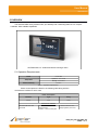
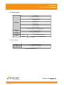
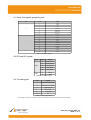
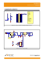
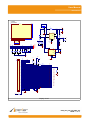
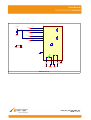
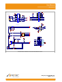
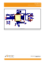
User Manual
APEXAR PRO
APEXAR EMBEDDED SOLUTION
APEXAR PRO
PRODUCTION MODULE
ENG_APX_020_005_MAN_001
PAGE: 1 of 19
User Manual
APEXAR PRO
CONTENT
1 OBJECTIVE................................................................................................................................................. 3
2 SCOPE........................................................................................................................................................ 3
3 REFERENCE............................................................................................................................................... 3
4 OVERAL DESCRIPTION............................................................................................................................. 3
5 OVERVIEW.................................................................................................................................................. 4
5.1 Operation Requirements...................................................................................................................... 4
5.2 Key Features........................................................................................................................................ 5
5.3 Dimensions.......................................................................................................................................... 5
6 OVERAL DESCRIPTION............................................................................................................................. 6
7 MECHANICAL SPECIFICATIONS............................................................................................................... 7
8 EXPANSION CONNECTOR PIN ASSIGNMENT......................................................................................... 8
9 SERIAL INTERFACES................................................................................................................................. 9
9.1 Serial Port signals grouped by port.................................................................................................... 10
9.2 SPI and I2C signals........................................................................................................................... 10
9.3 The debug port................................................................................................................................... 10
10 THE RESET SIGNAL............................................................................................................................... 11
11 THE NAND DISABLE BUTTON................................................................................................................ 11
12 MAINBOARD SCHEMATICS................................................................................................................... 12
NOTES.......................................................................................................................................................... 18
ENG_APX_020_005_MAN_001
PAGE: 2 of 19
User Manual
APEXAR PRO
1 OBJECTIVE
This manual presents all the characteristics and features of the APEXAR PRO family modules.
2 SCOPE
Applies for all the APEXAR PRO family modules.
3 REFERENCE
[1] ENG_APX_020_002_DOG_001 (Grabado y actualización de software).
4 OVERAL DESCRIPTION
We start with a global overview of the APEXAR PRO modules, in this secction you find the
operational requirements, dimensions and key features.
Then we will explore the main board of the APEXAR PRO module allowing you to get more familliar
with the available connectors.
The APEXAR PRO module was designed not only to be integrated with other hardware but also to
be expanded and customized. In the mechanical data section and expansion connector section along
with the module schematics you find all you need to build an expansion card if it's needed.
ENG_APX_020_005_MAN_001
PAGE: 3 of 19
User Manual
APEXAR PRO
5 OVERVIEW
The APEXAR PRO family modules offer you flexibility and outstanding features in a compact
hardware. With scalable capabilities.
APEXAR PRO 4.3” Production Module running a demo.
5.1 Operation Requirements
Power
9 a 24 VDC
Operation: -10 a +50 ºC
Temperature
Relative Humidity
Storage: -40 a +85 ºC
0 a 90 %
Table 1 – Operation Requierments.
Power consumptions are listed in the following table along with the
mesurement condition for each case.
Power Consumption
Minimum
Light
Heavy
2.5 W
5W
10 W
Measurment conditions
No external devices were
connected.
Two USB devices + Ethernet +
Audio Speaker.
Table 2 – Power consumption.
In reference with the main
voltage regulator power limit.
ENG_APX_020_005_MAN_001
PAGE: 4 of 19
User Manual
APEXAR PRO
5.2 Key Features
USB Host x 2
USB on the go x 1
Ethernet (10/100 Mbits/s) x 1
Serial RS485 x 1
Serial TTL x 3
Conectivity
serial RS232 x 1
serial DEBUG x 1
SPI x 1 (3.3V logic)
I2C x 1 (3.3V logic)
GPIO's 4 (default) – 17 (max) (3.3V logic)
4.3” with resistive touchscreen
Display
8” with resistive touchscreen
Storage
Audio
microSD (hinged Lid)
Inputs
Outputs
Line In, Microphone (MONO)
Speaker (1.5W), Line Out/Headphones
Table 3 – Key features.
5.3 Dimensions
Display size
heigth x width x depth
4.3”
135 mm x 75 mm x 27.5 mm
8”
205 mm x 156 mm x 38 mm
Table 4 – Physical dimensions.
ENG_APX_020_005_MAN_001
PAGE: 5 of 19
User Manual
APEXAR PRO
6 OVERAL DESCRIPTION
In this section we introduce the main connectors, push buttons and battery holder available in the
mainboard of the APEXAR PRO.
A closeup to the APEXAR PRO module mainboard.
1
Expansion connector
P2
2
Debug serial connector
P3
3
RESET and NAND_DISABLE buttons
BP1/BP2
4
Power connector
P1
5
USB (host) connector
J5/J7
6
3V Battery (CR1220) holder
BATT1
7
Ethernet RJ45 connector
J4
8
microSD memory slot
SL1
9
USB (on the go) connector
J6
10
APEXAR SOM slot
J1
11
Power LED
Table 5 – Mainboard overview.
TPL1
ENG_APX_020_005_MAN_001
PAGE: 6 of 19
User Manual
APEXAR PRO
7 MECHANICAL SPECIFICATIONS
Anchoring holes diameter: 3.25
All sizes are in mm.
ENG_APX_020_005_MAN_001
PAGE: 7 of 19
User Manual
APEXAR PRO
8 EXPANSION CONNECTOR PIN ASSIGNMENT
Pin#
Signal
1
+5V
2
HDDA (-)
3
GND
4
HDDA (+)
Direct pins (1)
5
PB19
TXD0/SPI0_NPCS2
√
6
PD31
TI0B1/PWM1
√
7
PB18
RXD0/SPI0_NPCS1
√ (default GPIO)
8
PB17
RTS0
√ (default GPIO)
9
PD17
CTS1
√ (default GPIO)
10
PD16
RTS1
√ (default GPIO)
11
PA21
TWCK0
√
12
PA20
TWD0
√
13
TXD 232
14
RXD 232
15
RTS 232
16
CTS 232
17
SPEAKER OUT (+)
18
SPEAKER OUT (-)
19
TXD 485 (-)
20
TXD 485 (+)
21
RXD 485 (+)
22
RXD 485 (-)
23
PB7
RXD2
√
24
PB6
TXD2
√
25
PB4
TXD1
√
26
PB5
RXD1
√
27
+3.3V
28
WAKE_UP
29
GND
30
RESET
31
MIC
32
LINE OUT (Right)
33
LINE OUT (Left)
34
LINE IN (Left)
35
LINE IN (Right)
36
PD27
SPI0_NPCS3
√
37
PB3
SPI0_NPCS0
√
38
PB2
SPI0_SPCK
√
39
PB1
SPI0_MOSI
√
PB0
SPI0_MISO
√
40
Table 6 – Expansion connector pin assigment.
(1) These signals come strait from the microprocesor of the APEXAR SOM module.
ENG_APX_020_005_MAN_001
PAGE: 8 of 19
User Manual
APEXAR PRO
9 SERIAL INTERFACES
The APEXAR PRO offers four serial ports with different features:
Name
Default electrical
levels supported
Connector
Components to be removed
for TTL levels support
DGBU (Debug)
RS232
P3
-
Port 0
RS485
P2
R25
Port 1
RS232
P2
R21, R22
Port 2
TTL
P2
Table 7 – Serial interfaces.
-
All the signals that belong to the ports 0, 1 and 2 are mapped to the expansion connector. The
debug port has it own dedicated connector.
By default the APEXAR PRO module serial ports are configured to operate according to the level
standards described above. However, TTL levels signals are available also for port 0 and port 1. This
change can be accomplished by removing from the PCB the associated components listed above.
WARNING: When using a serial port you must not use any of the other signals
associated with it for any other purpose.
Example: Consider the case you are using the serial port 1 thru the RS232 interface (pins:
13, 14, 15, 16). Then you can not use the pins intended for the TTL interface (pins: 9, 10,
25, 26).
ENG_APX_020_005_MAN_001
PAGE: 9 of 19
User Manual
APEXAR PRO
9.1 Serial Port signals grouped by port
PORT
P2 Pin#
0
1
2
Signal
5
TXD0
7
RXD0
8
RTS0
19
TXD 485 (-)
20
TXD 485 (+)
21
RXD 485 (+)
22
RXD 485 (-)
9
CTS1
10
RTS1
25
TXD1
26
RXD1
13
TXD 232
14
RXD 232
15
RTS 232
16
CTS 232
23
RXD2
24
TXD2
Table 8 – Serial port signals.
9.2 SPI and I2C signals
Port
SPI
I2C
P2 pin#
Signal
36
SPI0_NPCS3
37
SPI0_NPCS0
38
SPI0_SPCK
39
SPI0_MOSI
40
SPI0_MISO
11
TWCK0
12
TWD0
Table 9 – SPI and I2C signals.
9.3 The debug port
Pin#
Signal
2
Serial data output (TXD)
3
Serial data input (RXD)
5
Signal ground
7*
RTS (output)
8*
CTS (input)
1,4,6,9,10
NC
Table 10 – Debug port signals.
(*) This signal is connected to a fixed logic levels (for more details refer to the comunication interfaces schematic).
ENG_APX_020_005_MAN_001
PAGE: 10 of 19
User Manual
APEXAR PRO
10 THE RESET SIGNAL
This signal is connected to the reset line of the microprocessor present at the APEXAR SOM.
Driving it to a HI state will reboot the system.
This signal is available in the expansion connector (see expansion connector pin assignment).
You can generate a reset event by pressing the reset button located at the mainboard of the
APEXAR PRO module.
11 THE NAND DISABLE BUTTON
By holding this button the nand flash memory present at the APEXAR SOM will be disabled. This
procedure is necessary when the developer/production user wants to upload data to the nand flash, this
includes the bootstrap, the u-boot, the kernel and the root file system [1].
WARNING: Pressing or holding the nand disable button while the module is
operational may crash the system and also may corrupt some data loaded in the
NAND flash.
ENG_APX_020_005_MAN_001
PAGE: 11 of 19
User Manual
APEXAR PRO
12 MAINBOARD SCHEMATICS
PA20 (TWD0)
PA21 (TWCK0)
+3.3V
+3.3V
P2
+5V
GND_POWER
PB19
PB18
PD17
PA21
TXD_232
RTS_232
SPK_OUT2
TXD-_485
RXD+_485
PB7
PB4
+3.3V
GND_POWER
MIC1
LINE_OUT_L
LINE_IN_R
PB3
PB1
R5
1K
NRST
BP1
BP2
RESET
NAND_DSBL
GND_POWER
1
3
5
7
9
11
13
15
17
19
21
23
25
27
29
31
33
35
37
39
HDDA1_ N
HDDA1_ P
2
4
6
8
10
12
14
16
18
20
22
24
26
28
30
32
34
36
38
40
PD31
PB17
PD16
PA20
RXD_232
CTS_232
SPK_OUT1
TXD+_485
RXD-_485
PB6
PB5
WKUP
NRST
LINE_OUT_R
LINE_IN_L
PD27
PB2
PB0
R45
PB0 (SPI0_MISO)
PB1 (SPI0_MOSI)
PB2 (SPI0_SPCK)
PB3 (SPI0_NPCS0)
0 HDDA_N
HDDA_P
R46
0
PB4 (TXD1)
PB5 (RXD1)
PB6 (TXD2)
PB7 (RXD2)
PB17 (SPI1_NPCS0/RTS0)
PB18 (RXD0/SPI0_NPCS1)
PB19 (TXD0/SPI0_NPCS2)
PD16 (RTS1)
PD17 (CTS1)
PD27 (PCK1/SPI0_NPCS3)
PD31 (TIOB1/PWM1)
Header 20X2
Expansion connector; RESET and NAND_DISABLE switches.
GND_POWER
D5
3A 40V
P1
1
2
Header 2
GND_POWER
R53
U1
LM22675
VIN
C1
22uF 35V
7
NC
NC
BOOT
EN
SW
+5V
R54
4
U2
2
10K
1
C6
1
10nF
8
+3.3V
VIN
VOUT
SD
SENSE
3
R20
0
R57
33uH
0
D1
3A 40V
R19
10K
C7
150uF 10V
R47
10K
LP3875
C5
100nF
R1
330
C4
150uF 10V
TPL1
2
PAD 9
GND 6
L1
4
1
5
FB
GND 5
C2
2.2uF 35V
2
3
VIN
C8
100nF
GND_POWER
GND_POWER
GND_POWER
GND_POWER GND_POWER
Reemplazo para el
regulador de 5V
GND_POWER
TPS5420
+5V
R2
100K
VBAT
Q1
Si1563EDH
1
+
BATT1
-
GND_POWER
6
C10
GND_POWER
SHDN R3
10K
R4
5M
2
5
3
4
+5V
VBAT
Voltage regulators and 3V battery.
ENG_APX_020_005_MAN_001
PAGE: 12 of 19
User Manual
APEXAR PRO
4.3" 480x272
TFT LCD DISPLAY
LG PHILIPS
Z1
D2
BAR43C
L2
+5V
VLED+
C20
4.7uF
6
D6
20V
U3
SW
VIN
DIM
2
GND_POWER
3
R201
PGND
THP 1
AGND57
R200
PE2
R59
(LCDCC)
R58
FB
R52
1K
PE31
VLED-
PIN 45
PIN 1
GND_POWER
(AD2Yp)
XpLCD
YmLCD
(AD0Xp)
(AD3Ym)
XmLCD
(AD1Xm)
U9
C68
VIN
SW
C9
GND_POWER
GND_POWER
4
2
1
2
1
C3
PD22
PD20
PD23
PD21
R49
R50
D3
SM05
LM3410
R193 R192 R191 R190
YpLCD
C69
D4
SM05
1
A
K2
K1
A
K2
K1
CTRL
FB
COMP
THP 7
GND 3
3
3
GND_POWER
+5V
J3
pin40
XpLCD
pin39
YmLCD
pin38
XmLCD
pin37
YpLCD
pin36
10uF
2
GND_POWER
C71
220nF
GND_POWER
R48
R61
pin35
C72
5
PB15
R60
1
2
3
4
5
6
7
8
9
10
11
12
13
14
15
16
17
18
19
20
21
22
23
24
25
26
27
28
29
30
31
32
33
34
35
36
37
38
39
40
6
PB16
(pinxx = display pin number )
R62
pin34
(LCDDEN)
PE6
pin33
(LCDDVSYNC)
PE3
pin32
(LCDDHSYNC)
PE4
pin31
(LCDPWR)
PE0
(LCDDOTCK)
PE5
pin30
pin29
pin28
PE30
BLUE7
pin27
PE29
BLUE6
pin26
PE28
BLUE5
pin25
PE27
BLUE4
PE26
BLUE3
PE25
BLUE2
pin24
pin23
pin22
R18
PE24
BLUE1
pin21
PE23
BLUE0
pin20
PE22
GREEN7GND_POWER
pin19
PE21
GREEN6
PE20
GREEN5
PE19
GREEN4
pin18
pin17
pin16
PE18
GREEN3
pin15
PE17
GREEN2
pin14
PE16
GREEN1
pin13
PE15
GREEN0
PE14
RED7
PE13
RED6
pin12
pin11
pin10
PE12
RED5
pin9
PE11
RED4
pin8
PE10
RED3
pin7
PE9
RED2
PE8
RED1
PE7
RED0
pin6
pin5
pin4
pin3
C23
R55
pin2
VLED+
pin1
VLED-
GND_POWER
PD18
10uF
GND_POWER
4
Conductors
on
TOP SIDE
C21
10uH
C24
+3.3V
GND_POWER
R56
Dispaly circuit.
ENG_APX_020_005_MAN_001
PAGE: 13 of 19
User Manual
APEXAR PRO
J4
+AVDD3.3
C50
100nF
GND_ETH
TX_P
TX_N
RX_P
RX_N
TX_P
1
TD+
TX+
1
2
CT
TX_N
3
TD-
TX-
2
RX_P
4
RD+
RX+
3
5
CT
6
RD-
RX-
6
RX_N
1nF
.022uF
.022uF
R32
75
75
GND_ETH GND_POWER
4
75
5
1nF
75
8
7
8
GND_ETH
CASE9
10
+3.3V
11
13
12
R33
100
ETH_LED1 ETH_LED2
R34
100 GND_ETH
+3.3V
Ethernet circuit.
ENG_APX_020_005_MAN_001
PAGE: 14 of 19
User Manual
APEXAR PRO
+3.3V
MN1
1
+3.3V
+3.3V
16
SERIAL DEBUG PORT
C53
15
GND_POWER
GND_POWER
C1+
16
VCC
2
C57
VCC
C1+
1
3
4
C54
+3.3V
GND
C1V+
C2+
C56
3
4
R35
C52
6
V-
C2-
R38
C2+
GND_POWER
2
V+
C55
10
PD16
6
VT
T
14
TXD_232
7
RTS_232
13
RXD_232
8
CTS_232
R21
PB13
C2-
11
PB4
5
11
T
GND
C1-
C58
5
R37
14
15
R36
C59
C60
P3
Header 5X2A
7
10
T
12
PB5
R
R22
10
9
8
7
6
5
4
3
2
1
C51
U6
13
12
R
PB12
9
PD17
R
R39
8
9
R
C61
+3.3V
GND_POWER
USB HOST INTERFACE
2
USB_A
5
4
6
1
C62
U7
HDDA_N
3
HDDA_P
VCC
VCC
R25
J5
PB18
2
GND_POWER
3
4
PB19
5
6
7
GND_POWER
RXD+_485
12
11
R
PB17
14
13
R41
RXD-_485
10
9
D
NC
NC
GND
GND
TXD-_485
TXD+_485
1
8
ADM3491
+5V
GND_POWER
L5
U8
8
7
C63
C64
6
L6
5
GND_POWER
OUTA
ENA
IN
FLGA
GNG
FLGB
OUTB
ENB
1
(ENA)
2
(FLGA)
3
(FLGB)
4
(ENB)
PD1
PD2
PD4
PD3
C65
+3.3V
+5V
GND_POWER
D7
3A 40V
GND_POWER
+3.3V
R42
(VBUS)
R9
68K
PD0
R43
C66
ZX62-AB-5P
1
2
3
4
5
SHD
VBUS
DM
DP
ID
GND
GND_POWER
(IDUSB)
6
J6
C67
R7
68K
R8
10K
SL1
R11
1
PA5
27
R12
2
PA1
27
R13
3
27
GND_POWER
USB HOST/DEVICE INTERFACE
R10
68K
PA4
R44
7
R6
68K
HDDB_N
HDDB_P
PD28
PA0
4
R14
5
C19
27
+3.3V
PA2
R15
PA3
27
R16
100nF
CD/DAT3
CMD
VDD
0
CLK
VSS
GND_POWER
DAT0
DAT1
microSD slot
GND_POWER
J7
USB _A
6
2
5
1
4
7
8
27
GND_POWER
GND_POWER
6
DAT2
3
Comunication interfaces and microSD interface circuit.
ENG_APX_020_005_MAN_001
PAGE: 15 of 19
User Manual
APEXAR PRO
+3.3V_AC97
C25
C26
C27
C28
R23
R24
AGND_AC97
C29
C30
+3.3V
C31
C33
(AC97CK)
(AC97RX)
PD6
(AC97FS)
PD8
PD19
DVDD1
XTL_IN
XTL_OUT
DVSS1
SDATA_OUT
BIT_CLK
DVSS2
SDATA_IN
DVDD2
SYNC
RESET
NC1
C35
U5
+3.3V_AC97
LINE_OUT_R
LINE_OUT_L
AVDD4
AVSS4
AFILT4
AFILT3
AFILT2
AFILT1
VREFOUT
VREF
AVSS1
AVDD1
36
35
34
33
32
31
30
29
28
27
26
25
AGND_AC97
R27
C36
6
MONO_OUT
AVDD2
HP_OUT_L
AVSS2
HP_OUT_R
NC
AVDD3
AVSS3
ID0
ID1
EAPD
SPDIF
1
2
3
4
5
6
7
8
9
10
11
12
(AC97TX)
R26
+3.3V_AC97
C34
C37
PD7
PD9
37
38
39
40
41
42
43
44
45
46
47
48
U4
Y1
C32
VDD
LINE_OUT_R
LINE_OUT_L
4
-IN
3
+IN
2
Bypass
1
Shutdown
Vo1
5
SPK_OUT1
8
SPK_OUT2
C38
C39
C40
C41
C42
VREFOUT
C43
C44
Av=1
VDD/2
Vo2
C45
C46
Bias
GND
GND_POWER
+3.3V
L4
AGND_AC97
+3.3V_AC97
R40
C22
100
R51
C70
+3.3V_AC97
LINE_IN_R
100
C47
R30
7
L3
LINE_IN_R
24
LINE_IN_L
23
MIC2 22
MIC1 21
CD_ R 20
CD_GND_REF
19
CD_L 18
JS0 17
JS1 16
AUX_R15
AUX_L14
PHONE_IN
13
+5V
LINE_IN_L
R29
100
AGND_AC97
R28
2K2
MIC1
MIC1_GND
R31
AGND_AC97
GND_POWER
AGND_AC97
VREFOUT
C48
AGND_AC97
C49
100nF 1uF
AGND_AC97
Audio circuit.
ENG_APX_020_005_MAN_001
PAGE: 16 of 19
User Manual
APEXAR PRO
+3.3V
C11
100nF
C12
100nF
C13
100nF
C14
100nF
C15
100nF
C16
100nF
C17
100nF
C18
100nF
GND_POWER
PB15
PB15
PB13
PB13
PB12
PB12
PB4
PB4
PD16
PD16
TX_N
TX_P
RX_N
RX_P
ETH_LED2
+3.3V
PB5
PB5
PD17
PD17
PD1
PD1
PD2
PD2
PD4
PD4
PD3
PD3
PD28
PD28
PE31
+3.3V
GND_POWER
+3.3V
PE31
+3.3V
+3.3V
PD7
PD9
PD7
PD9
PD6
PD6
PD8
NRST
PD8
NRST
PD22
PD21
PD23
PD20
PD22
PD21
PD23
PD20
+3.3V
+3.3V
+3.3V
+3.3V
+3.3V
+3.3V
HDDA_P
HDDA_N
GND_POWER
HDDB_P
HDDB_N
+3.3V
GND_POWER
TX_N
2
TX_P
4
RX_N
6
RX_P
8
ETH_LED3 10
ETH_LED2 12
NC1
14
NC2
16
NC3
18
20
NC4
22
NC5
24
NC6
26
NC7
28
NC8
30
32
NC9
34
NC10
36
NC11
38
40
NC12
42
NC13
44
46
NC14
48
NC15
50
NC16
52
NC17
54
NC18
56
NC19
58
60
NC20
62
NC21
64
NC22
66
68
NC24
70
72
PA2
74
NC26
76
PA0
78
PA3
80
NC29
82
PD30
84
PD28
86
88
90
PD26
92
PD23
94
PD22
96
PB19
98
NC30
100
PB4
102
NC31
104
106
PB1
108
PB3
110
PD20
112
PD16
114
PA21
116
PB13
118
PD14
120
PD12
122
124
PD9
126
PD7
128
PE31
130
PE0
132
PD5
134
PD4
136
PD25
138
PD1
140
142
PE4
144
PE6
146
PE1
148
PE7
150
PE8
152
PE10
154
PE12
156
PE26
158
160
PE15
162
PE17
164
PE28
166
PE19
168
PE20
170
PE22
172
PE24
174
PB14
176
PB15
178
180
HDDA_P 182
HDDA_N 184
186
HDDB_P 188
HDDB_N 190
192
194
196
198
200
B1
B2
B3
B4
B5
B6
B7
B8
B9
B10
B11
B12
B13
B14
B15
B16
B17
B18
B19
B20
B21
B22
B23
B24
B25
B26
B27
B28
B29
B30
B31
B32
B33
B34
B35
B36
B37
B38
B39
B40
B41
B42
B43
B44
B45
B46
B47
B48
B49
B50
B51
B52
B53
B54
B55
B56
B57
B58
B59
B60
B61
B62
B63
B64
B65
B66
B67
B68
B69
B70
B71
B72
B73
B74
B75
B76
B77
B78
B79
B80
B81
B82
B83
B84
B85
B86
B87
B88
B89
B90
B91
B92
B93
B94
B95
B96
B97
B98
B99
B100
A1
A2
A3
A4
A5
A6
A7
A8
A9
A10
A11
A12
A13
A14
A15
A16
A17
A18
A19
A20
A21
A22
A23
A24
A25
A26
A27
A28
A29
A30
A31
A32
A33
A34
A35
A36
A37
A38
A39
A40
A41
A42
A43
A44
A45
A46
A47
A48
A49
A50
A51
A52
A53
A54
A55
A56
A57
A58
A59
A60
A61
A62
A63
A64
A65
A66
A67
A68
A69
A70
A71
A72
A73
A74
A75
A76
A77
A78
A79
A80
A81
A82
A83
A84
A85
A86
A87
A88
A89
A90
A91
A92
A93
A94
A95
A96
A97
A98
A99
A100
J1
SODIMM HEADER
1
3
+AVDD3.3
5
7
NC32
GND_ETH
9
NC33
11
ETH_LED1
GND_POWER
ETH_LED1
13
GND_POWER
15
NC34
17
19
21
23
25
27
29
31
33
35
37
39
41
43
45
47
49
51
53
55
57
59
61
63
65
67
69
71
73
75
77
79
81
83
85
87
89
91
93
95
97
99
101
103
105
107
109
111
113
115
117
119
121
123
125
127
129
131
133
135
137
139
141
143
145
147
149
151
153
155
157
159
161
163
165
167
169
171
173
175
177
179
181
183
185
187
189
191
193
195
197
199
NC35
NC36
NC37
NC38
NC39
NC40
NC41
NC42
NC43
NC44
NC45
NC46
NC47
NC48
NC49
GND_POWER
GND_POWER
GND_POWER
NC50
NC51
NC52
NC53
NAND_DSBL
NC54
NC55
NC56
PA4
PA1
PB17
NC60
PA5
PD31
PD29
NC62
PD27
NC63
PB6
PD21
PB18
PD19
PB5
PB7
PB0
PB2
PD17
PA20
PB12
PD15
PD13
PD11
PD10
PD8
PD6
PE30
PD18
PD3
PD2
PD0
PE3
PE5
PE2
PE25
PE9
PE11
PE27
PE13
PE14
PE16
PE18
PE29
PE21
PE23
PB16
WKUP
GND_POWER
GND_POWER
GND_POWER
GND_POWER
GND_POWER
GND_POWER
GND_POWER
SHDN
WAKE UP
EN_1V2
NRST
RTCK
TDO
NTRST
TDI
TCK
TMS
VBAT
GND_POWER
NRST
RTCK
TDO
NTRST
TDI
TCK
TMS
APX-SOM signals.
ENG_APX_020_005_MAN_001
PAGE: 17 of 19
User Manual
APEXAR PRO
NOTES
ENG_APX_020_005_MAN_001
PAGE: 18 of 19
User Manual
APEXAR PRO
Apexar Technologies S.A.
Estanislao Diaz 193 - (B1642EBC)
San Isidro | Buenos Aires | Argentina
TE: 54-11-4747-1616
www.apexar.com
ENG_APX_020_005_MAN_001
PAGE: 19 of 19