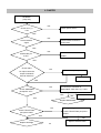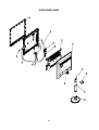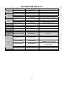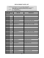
1
E-mail: http://www.LGEservice.com/techsup.html
COLOR MONITOR
SERVICE MANUAL
MODEL:
L1934S
(W1934S-BNT/SNT.AxxQQPH.
For CMO MODULE,
AxxVQPH. For AUO MODULE xx:sales marketing, Mstar
scaler)
CAUTION
BEFORE SERVICING THE UNIT,
READ THE SAFETY PRECAUTIONS IN THIS MANUAL.
*To apply the MSTAR Chip.
CONTENTS
SPECIFICATIONS ...................................................2
PRECAUTIONS .......................................................3
TIMING CHART .......................................................7
DISASSEMBLY ........................................................8
BLOCK DIAGRAM...................................................11
DISCRIPTION OF BLOCK DIAGRAM .................. 13
ADJUSTMENT ...................................................... 15
SERVICE OSD ........................................................16
TROUBLESHOOTING GUIDE .............................. 17
WIRING DIAGRAM ............................................... 23
EXPLODED VIEW...................................................24
REPLACEMENT PARTS LIST ...............................26
SCHEMATIC DIAGRAM ......................................... 34
SPECIFICATIONS
1. LCD CHARACTERISTICS
Type
: TFT Color LCD Module
Active Display Area : 19.0 inch
Pixel Pitch
: 0.285 (H) x 0.285 (V)
Color Depth
: 6bits, 16.7M colors
Size
: 428 (H) x 278 (V) x 16.2(D)
Electrical Interface
: LVDS
Surface Treatment
: Hard-coating(3H), Anti-Glare
Operating Mode
: Normally White, Transmissive mode
Backlight Unit
: 4-CCFL
4. Max. Resolution
D-sub Analog
5. POWER SUPPLY
5-1. Power : AC 100~240V, 50/60Hz , 0.8A
5-2. Power Consumption
MODE
Left : -80° min., -85°(Typ) Right : +80° min., +85°(Typ)
Top :+75° min., +80°(Typ) Bottom : -75° min., -80°(Typ)
: 220(min), 300(Typ) (Full White pattern, 0.7V) -6500K
: 170(min) (Full White pattern, 0.7V) -9300K
2-3. Contrast Ratio
: 630(min), 1000(Tye)
3. SIGNAL (Refer to the Timing Chart)
3-1. Sync Signal
• Type
: Separate Sync, SOG
3-2. Video Input Signal
1) Type
2) Voltage Level
a) Color 0, 0
b) Color 7, 0
c) Color 15, 0
3) Input Impedance
: R, G, B Analog
: 0~0.71 V
: 0 Vp-p
: 0.467Vp-p
: 0.714Vp-p
: 75Ω
H/V SYNC VIDEO POWER CONSUMPTION LED COLOR
36 W(Typical)
BLUE
STAND-BY
OFF/ON
OFF
less than 1 W
AMBER
SUSPEND
ON/OFF
OFF
less than 1 W
AMBER
DPMS OFF
OFF/OFF OFF
less than 1 W
AMBER
less than 1 W
OFF
POWER ON (NORMAL)
2. OPTICAL CHARACTERISTICS
2-1. Viewing Angle by Contrast Ratio > 10
2-2. Luminance
: 1440 x 900@75Hz
POWER S/W OFF
ON/ON ACTIVE
-
-
6. ENVIRONMENT
6-1. Operating Temperature : 10°C~35°C
(Ambient)
6-2. Relative Humidity
: 10%~80% (Non-condensing)
6-3. MTBF
: 50,000 HRS with 90% Confidence
Lamp Life
: 50,000 Hours(Min)
7. DIMENSIONS (with TILT/SWIVEL)
Width
Depth
Height
: 44.836 mm (17.65 inchs)
: 18.30 mm (7.20 inchs)
: 37.575 mm (14.79 inchs)
8. WEIGHT (with TILT/SWIVEL)
Net. Weight
3-3. Operating Frequency
Horizontal
: 30 ~ 83kHz
Vertical
: 56 ~ 75Hz
-2-
: 3.2 kg
(7.05 Ibs)
PRECAUTION
WARNING
WARNING FOR THE SAFETY-RELATED COMPONENT.
• There are some special components used in LCD
monitor that are important for safety. These parts are
marked on the schematic diagram and the
replacement parts list. It is essential that these critical
parts should be replaced with the manufacturer’s
specified parts to prevent electric shock, fire or other
hazard.
• Do not modify original design without obtaining written
permission from manufacturer or you will void the
original parts and labor guarantee.
BE CAREFUL ELECTRIC SHOCK !
• If you want to replace with the new backlight (CCFL) or
inverter circuit, must disconnect the AC adapter
because high voltage appears at inverter circuit about
650Vrms.
• Handle with care wires or connectors of the inverter
circuit. If the wires are pressed cause short and may
burn or take fire.
Leakage Current Hot Check Circuit
TAKE CARE DURING HANDLING THE LCD MODULE
WITH BACKLIGHT UNIT.
AC Volt-meter
• Must mount the module using mounting holes arranged
in four corners.
• Do not press on the panel, edge of the frame strongly
or electric shock as this will result in damage to the
screen.
• Do not scratch or press on the panel with any sharp
objects, such as pencil or pen as this may result in
damage to the panel.
• Protect the module from the ESD as it may damage the
electronic circuit (C-MOS).
• Make certain that treatment person’s body are
grounded through wrist band.
• Do not leave the module in high temperature and in
areas of high humidity for a long time.
• The module not be exposed to the direct sunlight.
• Avoid contact with water as it may a short circuit within
the module.
• If the surface of panel become dirty, please wipe it off
with a softmaterial. (Cleaning with a dirty or rough cloth
may damage the panel.)
CAUTION
Please use only a plastic screwdriver to protect yourself
from shock hazard during service operation.
-3-
Good Earth Ground
such as WATER PIPE,
CONDUIT etc.
To Instrument’s
exposed
METALLIC PARTS
1.5 Kohm/10W
SERVICING PRECAUTIONS
CAUTION: Before servicing receivers covered by this
service manual and its supplements and addenda, read
and follow the SAFETY PRECAUTIONS on page 3 of this
publication.
NOTE: If unforeseen circumstances create conflict
between the following servicing precautions and any of the
safety precautions on page 3 of this publication, always
follow the safety precautions. Remember: Safety First.
General Servicing Precautions
1. Always unplug the receiver AC power cord from the AC
power source before;
a. Removing or reinstalling any component, circuit
board module or any other receiver assembly.
b. Disconnecting or reconnecting any receiver electrical
plug or other electrical connection.
c. Connecting a test substitute in parallel with an
electrolytic capacitor in the receiver.
CAUTION: A wrong part substitution or incorrect
polarity installation of electrolytic capacitors may
result in an explosion hazard.
d. Discharging the picture tube anode.
2. Test high voltage only by measuring it with an
appropriate high voltage meter or other voltage
measuring device (DVM, FETVOM, etc) equipped with
a suitable high voltage probe.
Do not test high voltage by "drawing an arc".
3. Discharge the picture tube anode only by (a) first
connecting one end of an insulated clip lead to the
degaussing or kine aquadag grounding system shield
at the point where the picture tube socket ground lead
is connected, and then (b) touch the other end of the
insulated clip lead to the picture tube anode button,
using an insulating handle to avoid personal contact
with high voltage.
4. Do not spray chemicals on or near this receiver or any
of its assemblies.
5. Unless specified otherwise in this service manual,
clean electrical contacts only by applying the following
mixture to the contacts with a pipe cleaner, cottontipped stick or comparable non-abrasive applicator;
10% (by volume) Acetone and 90% (by volume)
isopropyl alcohol (90%-99% strength)
CAUTION: This is a flammable mixture.
Unless specified otherwise in this service manual,
lubrication of contacts in not required.
6. Do not defeat any plug/socket B+ voltage interlocks
with which receivers covered by this service manual
might be equipped.
7. Do not apply AC power to this instrument and/or any of
its electrical assemblies unless all solid-state device
heat sinks are correctly installed.
8. Always connect the test receiver ground lead to the
receiver chassis ground before connecting the test
receiver positive lead.
Always remove the test receiver ground lead last.
9. Use with this receiver only the test fixtures specified in
this service manual.
CAUTION: Do not connect the test fixture ground strap
to any heat sink in this receiver.
Electrostatically Sensitive (ES) Devices
Some semiconductor (solid-state) devices can be
damaged easily by static electricity. Such components
commonly are called Electrostatically Sensitive (ES)
Devices. Examples of typical ES devices are integrated
circuits and some field-effect transistors and
semiconductor "chip" components. The following
techniques should be used to help reduce the incidence of
component damage caused by static by static electricity.
1. Immediately before handling any semiconductor
component or semiconductor-equipped assembly, drain
off any electrostatic charge on your body by touching a
known earth ground. Alternatively, obtain and wear a
commercially available discharging wrist strap device,
which should be removed to prevent potential shock
reasons prior to applying power to the unit under test.
2. After removing an electrical assembly equipped with
ES devices, place the assembly on a conductive
surface such as aluminum foil, to prevent electrostatic
charge buildup or exposure of the assembly.
3. Use only a grounded-tip soldering iron to solder or
unsolder ES devices.
4. Use only an anti-static type solder removal device.
Some solder removal devices not classified as "antistatic" can generate electrical charges sufficient to
damage ES devices.
5. Do not use freon-propelled chemicals. These can
generate electrical charges sufficient to damage ES
devices.
6. Do not remove a replacement ES device from its
protective package until immediately before you are
ready to install it. (Most replacement ES devices are
packaged with leads electrically shorted together by
conductive foam, aluminum foil or comparable
conductive material).
7. Immediately before removing the protective material
from the leads of a replacement ES device, touch the
protective material to the chassis or circuit assembly
into which the device will be installed.
CAUTION: Be sure no power is applied to the chassis
or circuit, and observe all other safety precautions.
8. Minimize bodily motions when handling unpackaged
replacement ES devices. (Otherwise harmless motion
such as the brushing together of your clothes fabric or
the lifting of your foot from a carpeted floor can
generate static electricity sufficient to damage an ES
device.)
-4-
General Soldering Guidelines
1. Use a grounded-tip, low-wattage soldering iron and
appropriate tip size and shape that will maintain tip
temperature within the range or 500。F to 600。F.
2. Use an appropriate gauge of RMA resin-core solder
composed of 60 parts tin/40 parts lead.
3. Keep the soldering iron tip clean and well tinned.
4. Thoroughly clean the surfaces to be soldered. Use a
mall wire-bristle (0.5 inch, or 1.25cm) brush with a
metal handle.
Do not use freon-propelled spray-on cleaners.
5. Use the following unsoldering technique
a. Allow the soldering iron tip to reach normal
temperature.
(500。F to 600。F)
b. Heat the component lead until the solder melts.
c. Quickly draw the melted solder with an anti-static,
suction-type solder removal device or with solder
braid.
CAUTION: Work quickly to avoid overheating the
circuitboard printed foil.
6. Use the following soldering technique.
a. Allow the soldering iron tip to reach a normal
temperature (500。F to 600。F)
b. First, hold the soldering iron tip and solder the strand
against the component lead until the solder melts.
c. Quickly move the soldering iron tip to the junction of
the component lead and the printed circuit foil, and
hold it there only until the solder flows onto and
around both the component lead and the foil.
CAUTION: Work quickly to avoid overheating the
circuit board printed foil.
d. Closely inspect the solder area and remove any
excess or splashed solder with a small wire-bristle
brush.
IC Remove/Replacement
Some chassis circuit boards have slotted holes (oblong)
through which the IC leads are inserted and then bent flat
against the circuit foil. When holes are the slotted type,
the following technique should be used to remove and
replace the IC. When working with boards using the
familiar round hole, use the standard technique as
outlined in paragraphs 5 and 6 above.
Removal
1. Desolder and straighten each IC lead in one operation
by gently prying up on the lead with the soldering iron
tip as the solder melts.
2. Draw away the melted solder with an anti-static
suction-type solder removal device (or with solder
braid) before removing the IC.
-5-
Replacement
1. Carefully insert the replacement IC in the circuit board.
2. Carefully bend each IC lead against the circuit foil pad
and solder it.
3. Clean the soldered areas with a small wire-bristle
brush. (It is not necessary to reapply acrylic coating to
the areas).
"Small-Signal" Discrete Transistor
Removal/Replacement
1. Remove the defective transistor by clipping its leads as
close as possible to the component body.
2. Bend into a "U" shape the end of each of three leads
remaining on the circuit board.
3. Bend into a "U" shape the replacement transistor leads.
4. Connect the replacement transistor leads to the
corresponding leads extending from the circuit board
and crimp the "U" with long nose pliers to insure metal
to metal contact then solder each connection.
Power Output, Transistor Device
Removal/Replacement
1. Heat and remove all solder from around the transistor
leads.
2. Remove the heat sink mounting screw (if so equipped).
3. Carefully remove the transistor from the heat sink of the
circuit board.
4. Insert new transistor in the circuit board.
5. Solder each transistor lead, and clip off excess lead.
6. Replace heat sink.
Diode Removal/Replacement
1. Remove defective diode by clipping its leads as close
as possible to diode body.
2. Bend the two remaining leads perpendicular y to the
circuit board.
3. Observing diode polarity, wrap each lead of the new
diode around the corresponding lead on the circuit
board.
4. Securely crimp each connection and solder it.
5. Inspect (on the circuit board copper side) the solder
joints of the two "original" leads. If they are not shiny,
reheat them and if necessary, apply additional solder.
Fuse and Conventional Resistor
Removal/Replacement
1. Clip each fuse or resistor lead at top of the circuit board
hollow stake.
2. Securely crimp the leads of replacement component
around notch at stake top.
3. Solder the connections.
CAUTION: Maintain original spacing between the
replaced component and adjacent components and the
circuit board to prevent excessive component
temperatures.
Circuit Board Foil Repair
Excessive heat applied to the copper foil of any printed
circuit board will weaken the adhesive that bonds the foil
to the circuit board causing the foil to separate from or
"lift-off" the board. The following guidelines and
procedures should be followed whenever this condition is
encountered.
At IC Connections
To repair a defective copper pattern at IC connections use
the following procedure to install a jumper wire on the
copper pattern side of the circuit board. (Use this
technique only on IC connections).
1. Carefully remove the damaged copper pattern with a
sharp knife. (Remove only as much copper as
absolutely necessary).
2. carefully scratch away the solder resist and acrylic
coating (if used) from the end of the remaining copper
pattern.
3. Bend a small "U" in one end of a small gauge jumper
wire and carefully crimp it around the IC pin. Solder the
IC connection.
4. Route the jumper wire along the path of the out-away
copper pattern and let it overlap the previously scraped
end of the good copper pattern. Solder the overlapped
area and clip off any excess jumper wire.
At Other Connections
Use the following technique to repair the defective copper
pattern at connections other than IC Pins. This technique
involves the installation of a jumper wire on the
component side of the circuit board.
1. Remove the defective copper pattern with a sharp
knife.
Remove at least 1/4 inch of copper, to ensure that a
hazardous condition will not exist if the jumper wire
opens.
2. Trace along the copper pattern from both sides of the
pattern break and locate the nearest component that is
directly connected to the affected copper pattern.
3. Connect insulated 20-gauge jumper wire from the lead
of the nearest component on one side of the pattern
break to the lead of the nearest component on the
other side.
Carefully crimp and solder the connections.
CAUTION: Be sure the insulated jumper wire is
dressed so the it does not touch components or sharp
edges.
-6-
TIMING CHART
MODE
1
2
3
4
5
6
7
8
9
10
11
12
13
14
15
16
H/V
Sync
Polarity
H(Pixels)
V(Lines)
H(Pixels)
V(Lines)
H(Pixels)
V(Lines)
H(Pixels)
V(Lines)
H(Pixels)
V(Lines)
H(Pixels)
V(Lines)
H(Pixels)
V(Lines)
H(Pixels)
V(Lines)
H(Pixels)
V(Lines)
H(Pixels)
V(Lines)
H(Pixels)
V(Lines)
H(Pixels)
V(Lines)
H(Pixels)
V(Lines)
H(Pixels)
V(Lines)
H(Pixels)
V(Lines)
H(Pixels)
V(Lines)
+
+
+
+
+
+
+/+/+/+/+
+
+
+
+
+
+
Dot
Clock
25.175
28.321
25.175
31.5
40.0
49.5
57.2832
65.0
78.5
100.0
92.954
108.0
135.0
88.750
106.500
136.750
Frequency
Total
Period
(E)
31.469
70.08
31.469
70.08
31.469
59.94
37.5
75
37.879
60.317
46.875
75.0
49.725
74.553
48.363
60.0
60.023
75.029
68.681
75.062
61.805
65
63.981
60.02
79.976
75.035
55.469
59.901
55.935
59.887
70.635
74.984
800
449
900
449
800
525
840
500
1056
628
1056
625
1152
667
1344
806
1312
800
1456
915
1504
937
1688
1066
1688
1066
1600
926
1904
934
1936
942
-7-
Video
Active
Time
(A)
640
350
720
400
640
480
640
480
800
600
800
600
832
624
1024
768
1024
768
1152
870
1152
900
1280
1024
1280
1024
1400
900
1400
900
1400
900
Sync
Duration
(C)
Front
Porch
( D)
Back
Porch
(B)
96
2
108
2
96
2
64
3
128
4
80
3
61
3
136
6
96
3
32
3
30
2
112
3
144
3
32
6
152
6
152
6
96
2
108
2
8
2
16
1
40
1
16
1
64
3
24
3
16
1
128
3
128
4
48
1
16
1
48
3
80
3
96
3
48
60
52
35
40
25
120
16
88
23
160
21
224
37
160
29
176
28
144
39
194
31
248
38
248
38
80
17
232
25
248
33
Resolution
640 X 350
720 X 400
640 x 480
640 x 480
800 x 600
800 x 600
832 x 624
1024 x 768
1024 x 768
1152 x 870
1152 x 900
1280x1024
1280 x 1024
1440 x 900
1440 x 900
1440 x 900
DISASSEMBLY-Set
#2
#1
Put the monitor on a soft flat.
Pull out the hinge cover as arrow direction.
#3
#4
Remove the four screws.
Put the front cover upward. Then let the all latches
are separated.
#6
#5
Put the front face down, disassembly back cover.
Pull the key board out of bezel.
8
#8
#7
Disassembly the bezel.
Disassembly the connector and screw.
#10
#9
Remove the 2 screws.
Disassemble the LVDS cable
#12
#11
Main board and power board
The panel
9
DISASSEMBLY-Stand
#1
#2
Pull the Base 2 ea Latches to inside until losing elasticity.
#3
Consequently, pull the stand body directly.
#4
Separate Stand Body & Stand Base.
Fix Stand Base & Stand Body.
#5
#6
Remove the three screws.
Separate the hinge and stand.
10
TSUM1PFR
BLOCK DIAGRAM
11
BLOCK DIAGRAM-POWER
Power
5V
100~240V
EMI filter
Rush
Rectification
Diode
Transformer
prevention
rectifier
12V
Starting
resistor
5V/12V
Feedback
output OVP
control
Switching
circuit
circuit (PWM
OVP protect
control IC &
circuit
MOSFER)
Inverter
12V
Push-pull
Transformer
circuit
conversion
OVP circuit
VDDA
ON/OFF
ON/OFF circuit
DIM
LC resonance
PWM IC
Feedback
OZ9938GN
circuit
DIM circuit
12
4 CCFL lamps
Sampling
Lamp open
protection
DESCRIPTION OF BLOCK DIAGRAM
1. Video Controller Part.
This part amplifies the level of video signal for the digital conversion and converts from the analog video signal to the
digital video signal using a pixel clock.
The pixel clock for each mode is generated by the PLL.
The range of the pixel clock is from 25MHz to 135MHz.
This part consists of the Scaler, ADC converter, TMDS receiver and LVDS transmitter.
The Scaler gets the video signal converted analog to digital, interpolates input to 1280 X 1024 resolution signal and
outputs 8-bit R, G, B signal to transmitter.
2. Power Part.
This part consists of the one 3.3V, and one 1.8V regulators to convert power which is provided 5V in Power board.
12V is provided for inverter, 5V is provided for LCD panel.
Also, 5V is converted 3.3V and 1.8V by regulator. Converted power is provided for IC in the main board.
The inverter converts from DC 12V to AC 700Vrms and operates back-light lamps of module.
3. MICOM Part.
This part is including video controller part. And this part consists of EEPROM IC which stores control data, Reset IC and
the Micom.
The Micom distinguishes polarity and frequencies of the H/V sync are supplied from signal cable.
The controlled data of each mode is stored in EEPROM.
13
LIPS Board Block Diagram
Operation description_LIPS
1. EMI components.
This part contains of EMI components to comply with global marketing EMI standards like FCC,VCCI CISPR, the
circuit included a line-filter, across line capacitor and of course the primary protection fuse.
2. Input rectifier and filter.
This part function is for transfer the input AC voltage to a DC voltage through a bridge rectifier and a bulk capacitor.
3. Energy Transfer.
This part function is for transfer the primary energy to secondary through a power transformer.
4. Output rectifier and filter.
This part function is to make a pulse width modulation control and to provide the driver signal to power switch, to
adjust the duty cycle during different AC input and output loading condition to achieve the dc output stabilized, and
also the over power protection is also monitor by this part.
5. Photo-Coupler isolation.
This part function is to feed back the DC output changing status through a photo transistor to primary controller to
achieve the stabilized DC output voltage.
6. Signal collection.
This part function is to collect the any change from the DC output and feed back to the primary through photo transistor.
14
ADJUSTMENT
Windows EDID V1.0 User Manual
example, your monitor use the CMO Panel ,then you
Operating System: DOS, windows98, 2000, XP
should assure a certain digit(usually the sixteenth or
seventeenth digit for LG) of your input panel check
1. Parallel port setting
number is ‘q’ or ‘Q’.
Enter your bios,and do as followings.
a) Integrated peripheral
b) Super IO Device
c) Parallel port mode
you should set the” parallel port mode” to SPP for using
the DOS EDID tool surely.
2. EDID Write
① Run D20FNL.EXE.
And choose 1 to write.
④ input serial NO.
② choose panel type
For LG , the number of SN is 12. So input 12 digits,then
EDID data will be send to the monitor from PC.
③ if you get the right panel type, the you can go to the
next step; if not ,the panel type loop will continue. For
15
SERVICE MODE
1) Turn off the power switch at the front side of the display.
2) Wait for about 5 seconds and press MENU, POWER switch with 1 second interval.
3) The SVC OSD menu contains additional menus that the User OSD menu as described below.
a) CLEAR ETI: To initialize using time.
b) Auto Color: W/B balance and automatically sets the gain and offset value.
c) AGING: Select Aging mode (on/off).
d) PANEL: used panel type
e) NVRAM INIT: EEPROM initialize. (24C08)
f) R/G/B-9300K: Allows you to set the R/G/B-9300K value manually.
g) R/G/B-6500K: Allows you to set the R/G/B-6500K value manually.
h) R/G/B-Offset: Allows you to set the R/G/B-Offset value manually. (Analog Only)
i) R/G/B-Gain: Allows you to set the R/G/B-Gain value manually. (Analog Only)
Connect to
Connect to
the monitor
the PC
Figure 1. Cable Connection for Micom uploading
16
TROUBLESHOOTING GUIDE
1. NO POWER
No Power
(Power Indicator Off)
NO
Please reinsert and
make sure the AC of
Check the Adapter/Inverter
section
90-264v is normal
YES
NO
Measure C423 (+)
=1.8V
Check CN404 or replace
Q409, Q410, and U404
U404 PIN2=3.3V
YES
NO
Check X401 oscillate
waveforms are normal
YES
Replace U401
17
Replace X401
2. NO RASTER (OSD IS NOT DISPLAY)-LIPS
No Raster
(OSD Is Not Displayed)
NO
Check power board and find out a
Check U404
short point as penning each power
PIN 3 =5V?
line
YES
Check U404
NO
PIN 2 =3.3V?
1.
Check U404
2.
Check C426,C427
YES
CheckC423 (+)
NO
1. Check Q409,Q410
2. Check C432,C423
1.8V?
3.
TROUBLE IN SCALER IC
YES
NO
Check CN701
Check BL ON/OFF pulse as
PIN1 =5V?
contacting scope
YES
LIPS
18
2. NO RASTER (OSD IS NOT DISPLAY)-MSTAR
No Raster
(OSD Is Not Displayed)
SCALER PIN1,2
NO
1. Check C411 C412
OSCILLATES AS
2. Check X401
14.318MHZ?
3. TROUBLE IN SCALER IC
YES
SCALER IC
NO
CHECK CONNECTION
PIN16 H SYNC ?
LINE FROM D-SUB TO
PIN17 V SYNC?
SCALER
YES
TROUBLE IN CABLE OR
LCD MODULE
19
4. TROUBLE IN DPM
TROUBLE IN DPM
NO
SCALER IC
PIN16 H SYNC?
CHECK H/V SYNC LINE
PIN17 V SYNC?
YES
TROUBLE IN CABLE OR
LCD MODULE
20
5. POWER
No Power
(Power Indicator Off)
NO
Check AC line
Check AC line
volt
YES
NO
Check F901, BD901
Check the
voltage of C905(+)
YES
NO
Check start voltage
Check D905, R934,
for the pin1 of
R928,IC901
IC901
YES
NO
Check IC901 pin 7
Vcc is 13v?
Check D902,C907
YES
NO
Check IC901 PIN6
output is PWM?
Check D901,Q903,ZD904
Check IC901, T901,D907,D908,ZD903,ZD902,ZD901,IC902,IC903
21
6. RASTER
NO Raster
(Lamp Off)
NO
Check C811 (+)
Check power section
=12V
YES
NO
Check Interface section or
Check ON/OFF
main board
signal
YES
NO
Check Q801 Q802 Q803
CheckIC801 pin
ZD801
2=5V?
YES
Check IC801
NO
Check IC801 pin 5/pin6
Pin1/pin15 have the
output of sawtooth
NO
wave at short time
Replace IC801
YES
NO
Check Q805/Q806
Cut all the pin connector of
Q805/Q806, check C811 (+) =12V?
pin5/pin8 is 12V?
YES
YES
NO
Check Q801 Q802
Replace Q805/Q806
NO
Check PT801/PT802
Unplug backlight connector wire,
check PT801/PT802 pin7/pin8 =
pin7/pin8= 650V?
650V?
YES
NO
Replace PT801/PT802
Replace backlight
22
WIRING DIAGRAM
89G179E30N586
95G 825 7W503
89G 76J 8526
23
EXPLODED VIEW
24
EXPLODED VIEW PARTS LIST
Ref. No.
TPV part no.
LGE part no.
Description
A34G0563ABNA1B0100
ABJ55934301
Bezel (Front cabinet) Silver color
A34G0563 B6A1B0100
ABJ55934302
Bezel (Front cabinet) Black color
KEPC7QG8
EBU51011201
KEY BOARD include control wire
750GLM90A1A12N
COV30013601
CMO PANEL M190A1-L0A C1 NB
750GLV90W1021N
COV30024802
AUO PANEL TPM190A1-PW01 V0
PWPC942MG1
EBU51011301
POWER BOARD
CBPC7MMRLGQ1
EBU51011401
MAIN BOARD FOR CMO
CBPC84M5LGQ1
COV30024503
MAIN BOARD FOR AUO
060
Q15G0270101
MDQ48211901
MAIN FRAME
070
89G179E30N586
COV30013701
LVDS FFC Cable
080
A34G0564 B6 1B0100
ACQ55937401
REAR COVER
090
A37G0061 1
AGU55931102
HINGE ASS’Y
100
A34G0565 B6 1B0100
MCK48193801
STAND NECK
110
A34G0566 B6 1B0132
MCK48194001
STAND COVER
120
A34G0567 B6 1B0132
MCK48194201
BASE
130
A33G0317 B6 1L0100
MCK48193401
HINGE COVER
89G421A18N IS
6410TEW003A
89G402A18NIS
6410TUW008A
89G410A-18N-IS
6410TBW004A
89G420A-18N-IS
6410TTW001A
POWER CORD BLK 6ft For Taiwan
89G412A-18N-IS3
6410TSW003A
POWER CORD BLK 6ft For Australia
89G 728CAA 2G
COV30013801
SIGNAL CABLE
010
020
030
040
050
140
150
25
POWER CORD BLK 6FT For
Europe/Thailand/Vietnam/Russia/U.A.E
POWER CORD BLK 6FT For
USA/Mexico/Panama/Canada
POWER CORD 10A/250V BLK 6FT UK
for UK/Malaysia
REPLACEMENT PARTS LIST
DATE: 2008. 01. 27
*S
*AL
LOC. NO.
PART NO.
DESCRIPTION
MAIN BOARD
CAPACITORS
C427
067G 3151014KV
EC 105℃ CAP 100UF M 25V
C426
067G 3151014KV
EC 105℃ CAP 100UF M 25V
C423
067G 3151014KV
EC 105℃ CAP 100UF M 25V
C421
067G 3151014KV
EC 105℃ CAP 100UF M 25V
C410
067G215V100 7R
LOW E.S.R 10UF +/-20% 50V
C432
065G0402104 15
MLCC 0402 0.1UF K 16V X5R
C428
065G0402104 15
MLCC 0402 0.1UF K 16V X5R
C422
065G0402104 15
MLCC 0402 0.1UF K 16V X5R
C420
065G0402104 15
MLCC 0402 0.1UF K 16V X5R
C419
065G0402104 15
MLCC 0402 0.1UF K 16V X5R
C417
065G0402104 15
MLCC 0402 0.1UF K 16V X5R
C416
065G0402104 15
MLCC 0402 0.1UF K 16V X5R
C415
065G0402104 15
MLCC 0402 0.1UF K 16V X5R
C414
065G0402104 15
MLCC 0402 0.1UF K 16V X5R
C413
065G0402104 15
MLCC 0402 0.1UF K 16V X5R
C409
065G0402104 15
MLCC 0402 0.1UF K 16V X5R
C407
065G0402104 15
MLCC 0402 0.1UF K 16V X5R
C406
065G0402104 15
MLCC 0402 0.1UF K 16V X5R
C404
065G0402104 15
MLCC 0402 0.1UF K 16V X5R
C403
065G0402104 15
MLCC 0402 0.1UF K 16V X5R
C401
065G0402104 15
MLCC 0402 0.1UF K 16V X5R
C412
065G0402220 31
CHIP 22PF 50V NPO
C411
065G0402220 31
CHIP 22PF 50V NPO
C103
065G0402220 31
CHIP 22PF 50V NPO
C102
065G0402220 31
CHIP 22PF 50V NPO
C408
065G0402224 17
CAP CER 0.22UF -20%-80%
C429
065G0402224 17
CAP CER 0.22UF -20%-80%
C113
065G0402473 12
CHIP 0.047uF 16V X7R
C110
065G0402473 12
CHIP 0.047uF 16V X7R
C109
065G0402473 12
CHIP 0.047uF 16V X7R
C107
065G0402473 12
CHIP 0.047uF 16V X7R
C106
065G0402473 12
CHIP 0.047uF 16V X7R
C105
065G0402473 12
CHIP 0.047uF 16V X7R
C101
065G0402473 12
CHIP 0.047uF 16V X7R
26
C104
065G0402509 31
CHIP 5pF 50V NPO
C108
065G0402509 31
CHIP 5pF 50V NPO
C111
065G0402509 31
CHIP 5pF 50V NPO
ZD103
093G 39S 34 T
UDZSNP5.6B ROHM
ZD104
093G 39S 34 T
UDZSNP5.6B ROHM
D402
093G3004 3
SM340A
U401
056G 562557
IC TSUM1PFR-LF
U404
056G 563 52
IC AP1117D33LA TO252-3L ATC
U102
056G 662 13
IC AZC099-04S SOT23-6L
U103
056G 662 13
IC AZC099-04S SOT23-6L
U403
056G1133 32
IC M24C04-WMN6TP SO8
DIODEs
IC
U402
056G1133
SST25VF010A-33-4C-SAE
74(WLGMRT9MCQ1)
TRANSISTOR
Q404
057G 417 6
PMBS3906/PHILIPS-SMT(06)
Q406
057G 417 12 T
KEC 2N3904S-RTK/PS
Q410
057G 417 22 T
TRA KN2907AS -60V/-0.6A SOT-23
Q409
057G 417 22 T
TRA KN2907AS -60V/-0.6A SOT-23
Q405
057G 763 1
A03401 SOT23 BY AOS(A1)
R458
061G0402000
RST CHIPR 0 OHM +-5% 1/16W
R431
061G0402000
RST CHIPR 0 OHM +-5% 1/16W
R429
061G0402000
RST CHIPR 0 OHM +-5% 1/16W
R402
061G0402000
RST CHIPR 0 OHM +-5% 1/16W
R401
061G0402000
RST CHIPR 0 OHM +-5% 1/16W
R411
061G0402101
RST CHIPR 100 OHM +-5% 1/16W
R412
061G0402101
RST CHIPR 100 OHM +-5% 1/16W
R413
061G0402101
RST CHIPR 100 OHM +-5% 1/16W
R418
061G0402101
RST CHIPR 100 OHM +-5% 1/16W
R419
061G0402101
RST CHIPR 100 OHM +-5% 1/16W
R424
061G0402101
RST CHIPR 100 OHM +-5% 1/16W
R442
061G0402101
RST CHIPR 100 OHM +-5% 1/16W
R456
061G0402101
RST CHIPR 100 OHM +-5% 1/16W
R457
061G0402101
RST CHIPR 100 OHM +-5% 1/16W
R451
061G0402101
RST CHIPR 100 OHM +-5% 1/16W
R452
061G0402101
RST CHIPR 100 OHM +-5% 1/16W
R102
061G0402101
RST CHIPR 100 OHM +-5% 1/16W
R103
061G0402101
RST CHIPR 100 OHM +-5% 1/16W
R104
061G0402101
RST CHIPR 100 OHM +-5% 1/16W
R108
061G0402101
RST CHIPR 100 OHM +-5% 1/16W
R110
061G0402101
RST CHIPR 100 OHM +-5% 1/16W
R111
061G0402101
RST CHIPR 100 OHM +-5% 1/16W
R113
061G0402101
RST CHIPR 100 OHM +-5% 1/16W
RESISTORs
27
R114
061G0402101
RST CHIPR 100 OHM +-5% 1/16W
R115
061G0402101
RST CHIPR 100 OHM +-5% 1/16W
R117
061G0402101
RST CHIPR 100 OHM +-5% 1/16W
R405
061G0402101
RST CHIPR 100 OHM +-5% 1/16W
R441
061G0402102
RST CHIPR 1 KOHM +-5% 1/16W
R118
061G0402102
RST CHIPR 1 KOHM +-5% 1/16W
R121
061G0402103
RST CHIPR 10 KOHM +-5% 1/16W
R120
061G0402103
RST CHIPR 10 KOHM +-5% 1/16W
R455
061G0402103
RST CHIPR 10 KOHM +-5% 1/16W
R454
061G0402103
RST CHIPR 10 KOHM +-5% 1/16W
R453
061G0402103
RST CHIPR 10 KOHM +-5% 1/16W
R439
061G0402103
RST CHIPR 10 KOHM +-5% 1/16W
R437
061G0402103
RST CHIPR 10 KOHM +-5% 1/16W
R433
061G0402103
RST CHIPR 10 KOHM +-5% 1/16W
R421
061G0402103
RST CHIPR 10 KOHM +-5% 1/16W
R417
061G0402103
RST CHIPR 10 KOHM +-5% 1/16W
R408
061G0402103
RST CHIPR 10 KOHM +-5% 1/16W
R407
061G0402103
RST CHIPR 10 KOHM +-5% 1/16W
R406
061G0402103
RST CHIPR 10 KOHM +-5% 1/16W
R404
061G0402103
RST CHIPR 10 KOHM +-5% 1/16W
R436
061G0402104
RST CHIPR 100 KOHM +-5% 1/16W
R414
061G0402121
RST CHIP 120R 1/16W 5%
R410
061G0402121
RST CHIP 120R 1/16W 5%
R409
061G0402203
RST CHIP 20K 1/16W 5%
R105
061G0402222
RST CHIPR 2.2 KOHM +-5% 1/16W
R106
061G0402222
RST CHIPR 2.2 KOHM +-5% 1/16W
R109
061G0402390 0F
RST CHIP 390R 1/16W 1%
R403
061G0402390 0F
RST CHIP 390R 1/16W 1%
R427
061G0402392
RST CHIP 3.9K 1/16W 5%
R428
061G0402392
RST CHIP 3.9K 1/16W 5%
R435
061G0402472
RST CHIPR 4.7 KOHM +-5% 1/16W
R440
061G0402472
RST CHIPR 4.7 KOHM +-5% 1/16W
R116
061G0402750
RST CHIPR 75 OHM +-5% 1/16W
R112
061G0402750
RST CHIPR 75 OHM +-5% 1/16W
R107
061G0402750
RST CHIPR 75 OHM +-5% 1/16W
R101
061G0603000
RST CHIPR 0 OHM +-5% 1/10W
R434
061G1206331
RST CHIPR 330 OHM +-5% 1/4W
FB402
071G 56K121 M
CHIP BEAD
FB401
071G 56V301 B
CHIP BEAD FCM2012VF-301T07 bullwill
FB101
071G 59K190 B
19 OHM BEAD
FB102
071G 59K190 B
19 OHM BEAD
FB103
071G 59K190 B
19 OHM BEAD
X401
093G 22 53 J
14.31818MHZ/32PF/49US
COILs & FILTERs
OTHERs
28
CN404
033G3802 9
WAFER 9P RIGHT ANELE PITCH
CN402
033G8019 8C
FPC/FFC CONN
CN403
033G801930F CH JS
CONNECTOR
CN101
088G 35315F H
D-SUB 15PIN
C903
063G107K474 6S
CAP X2 0.47UF K 275VAC
C840
065G 3J3096ET
3PF,J,3KV,Z5P
C839
065G 3J3096ET
3PF,J,3KV,Z5P
C826
065G 3J3096ET
3PF,J,3KV,Z5P
C824
065G 3J3096ET
3PF,J,3KV,Z5P
C816
065G 6J1206ET
12PF 5% SL 6KV TDK
C825
065G 6J1206ET
12PF 5% SL 6KV TDK
C902
065G306M2222BP
2200PF +-20% 400VAC
C901
065G306M2222BP
2200PF +-20% 400VAC
C900
065G306M3322BP
3300PF 20%
C923
067G215S1023KV
105℃ 1000UF M 16V
C915
067G215V471 4H
CAP 105℃ 470UF M 25V
C920
067G215V471 4H
CAP 105℃ 470UF M 25V
C905
067G315Y10115H
CAP 105℃ 100uF M 450V
C815
067T215P4714XV
CAP 105℃ 470UF M 25V
C811
067T215P4714XV
CAP 105℃ 470UF M 25V
C808
061G0805184
RST CHIPR 180 KOHM +-5% 1/8W
C932
065G0603102 32
1000PF +-10% 50V X7R
C836
065G060347141J
W
CAP CHIP 0603 470PF J 100V NPO
C835
065G060347141J
W
CAP CHIP 0603 470PF J 100V NPO
C834
065G060347141J
W
CAP CHIP 0603 470PF J 100V NPO
C833
065G060347141J
W
CAP CHIP 0603 470PF J 100V NPO
C813
065G0805102 31
1000PF 50V NPO
C812
065G0805102 31
1000PF 50V NPO
C910
065G0805103 32
10NF/50V/0805/X7R
C807
065G0805103 32
10NF/50V/0805/X7R
C904
065G0805104 32
CHIP 0.1U 50V X7R
C832
065G0805104 32
CHIP 0.1U 50V X7R
C829
065G0805104 32
CHIP 0.1U 50V X7R
C828
065G0805104 32
CHIP 0.1U 50V X7R
C822
065G0805104 32
CHIP 0.1U 50V X7R
C821
065G0805104 32
CHIP 0.1U 50V X7R
C817
065G0805104 32
CHIP 0.1U 50V X7R
C802
065G0805104 32
CHIP 0.1U 50V X7R
C801
065G0805104 32
CHIP 0.1U 50V X7R
C908
065G0805104 32
CHIP 0.1U 50V X7R
C913
065G0805104 32
CHIP 0.1U 50V X7R
C918
065G0805104 32
CHIP 0.1U 50V X7R
C919
065G0805104 32
CHIP 0.1U 50V X7R
POWER BOARD
CAPACITORS
29
C814
065G0805105 22
CHIP 1UF 25V X7R 0805
C830
065G0805105 22
CHIP 1UF 25V X7R 0805
C806
065G0805105 22
CHIP 1UF 25V X7R 0805
C804
065G0805105 22
CHIP 1UF 25V X7R 0805
C914
065G0805152 32
CHIP 1500PF 50V X7R 0805
C912
065G0805152 32
CHIP 1500PF 50V X7R 0805
C909
065G0805221 31
220PF 50V NPO
C805
065G0805222 31
0805 2200PF
C837
065G0805391 31
CHIP 390PF 50V
C842
065G0805472 32
4700PF/50V/0805/X7R
C841
065G0805472 32
4700PF/50V/0805/X7R
C827
065G0805472 32
4700PF/50V/0805/X7R
C820
065G0805472 32
4700PF/50V/0805/X7R
C838
065G0805473 32
CHIP 0.047UF 50V X7R
C809
065G0805473 32
CHIP 0.047UF 50V X7R
C819
065G0805473 32
CHIP 0.047UF 50V X7R
C810
065G080556131G
MLCC 0805 560PF G 50V NPO
C905
006G 31502
1.5MM RIVET
C903
006G 31502
1.5MM RIVET
C934
065G 2K152 1T GP
CERAMIC CAP
C931
065G 2K152 1T GP
CERAMIC CAP
C930
065G 2K222 2T6921
CAP CER 2200PF K 2KV Y5P
C907
067G 5152207HT
CAP 105℃ 22UF M 50V
C922
067G215D4713KT
/105℃ EC 470UF M 16V KINGNICHI
C925
067G215S10915T3964
EC CAP 1.0uF 450V 8*11mm
BD901
093G 50460 38
BRIDGE KBJ408G 4A/800V KBJ
D908
093G3006 1 1
31DQ06FC3 NIHON INTER
D907
093G 60267
SP10100
D807
093G 6432S
IN4148W
D808
093G 6432S
IN4148W
D812
093G 6432S
IN4148W
D811
093G 6432S
IN4148W
D810
093G 6432S
IN4148W
D809
093G 6432S
IN4148W
D806
093G 6433S
DIODE BAV99 SEMTECH
D805
093G 6433S
DIODE BAV99 SEMTECH
D804
093G 6433S
DIODE BAV99 SEMTECH
D803
093G 6433S
DIODE BAV99 SEMTECH
D802
093G 6433S
DIODE BAV99 SEMTECH
D801
093G 6433S
DIODE BAV99 SEMTECH
ZD904
093G 39GA31 T
ZENER DIODE RLZ18B SEMTECH
ZD902
093G 39S 24 T
RLZ 5.6B LLDS
ZD801
093G 39S 24 T
RLZ 5.6B LLDS
ZD903
093G 39S 40 T
RLZ 13B LLDS
DIODEs
30
ZD901
093G 39S 40 T
RLZ 13B LLDS
ZD906
093G 39S 42 T
RLZ27B LLDS
BD901
006G 31500
EYELET
D905
093G 5212T52T
DIODE 1N4007 DO-41
D901
093G 6026W52T
FR107
D902
093G 6038T52T
FR103
D903
095G 90 23
JUMPER
IC902
056G 139 7 1
IC EL817MA M-TYPE
IC901
056G 379 79
IC LD7522PS SOP-8
IC801
056G 608 10
IC OZ9938GN-B SOIC-16
IC903
056G 158 12
KIA431A-AT/P TO-92
Q903
057G 667 47
FET FQPF8N60C FAIRCHILD
Q904
057G 417 4
PMBS3904/PHILIPS-SMT(04)
Q803
057G 417 4
PMBS3904/PHILIPS-SMT(04)
Q802
057G 417 4
PMBS3904/PHILIPS-SMT(04)
Q801
057G 417 4
PMBS3904/PHILIPS-SMT(04)
Q804
057G 759 2
RK7002
Q807
057G 759 2
RK7002
Q808
057G 759 2
RK7002
Q809
057G 759 2
RK7002
Q810
057G 759 2
RK7002
Q811
057G 759 2
RK7002
Q812
057G 759 2
RK7002
Q806
057G 763 6
AO4828L
Q805
057G 763 6
AO4828L
Q903
006G 31502
1.5MM RIVET
061G 58005 W
RST NTCR 5 OHM 3A THINKING
R937
061G0805102
RST CHIPR 1KOHM +-5% 1/8W
R926
061G0805102
RST CHIPR 1KOHM +-5% 1/8W
R922
061G0805102
RST CHIPR 1KOHM +-5% 1/8W
R921
061G0805102
RST CHIPR 1KOHM +-5% 1/8W
R843
061G0805102
RST CHIPR 1KOHM +-5% 1/8W
R836
061G0805102
RST CHIPR 1KOHM +-5% 1/8W
R927
061G0805103
10 KOHM 1/10W
R812
061G0805103
10 KOHM 1/10W
R806
061G0805103
10 KOHM 1/10W
R804
061G0805103
10 KOHM 1/10W
R803
061G0805103
10 KOHM 1/10W
R815
061G0805104
RST CHIP 100K 1/8W 5%
R839
061G0805105
1MOHM 1/10W
R840
061G0805105
1MOHM 1/10W
R844
061G0805105
1MOHM 1/10W
R847
061G0805105
1MOHM 1/10W
TRANSISTORs & ICs
RESISTORs
NR901
31
R838
061G0805105
1MOHM 1/10W
R820
061G0805105
1MOHM 1/10W
R813
061G0805105
1MOHM 1/10W
R816
061G0805105
1MOHM 1/10W
R810
061G0805105
1MOHM 1/10W
R913
061G0805124
RST CHIPR 120 KOHM +-5% 1/8W
R817
061G0805200 2F
RST CHIPR 20 KOHM +-1% 1/8W
R908
061G0805202
RST CHIP 2K 1/8W 5%
R924
061G0805240 1F
RST CHIPR 2.4KOHM +-1% 1/8W
R920
061G0805302
RST CHIPR 3 KOHM +-5% 1/8W
R802
061G0805304
RST CHIPR 300 KOHM +-5% 1/8W
R923
061G0805330 2F
RST CHIPR 33 KOHM +-1% 1/8W
R925
061G0805360 1F
RST CHIPR 3.6KOHM +-1% 1/8W
R826
061G0805390 0F
RST CHIPR 390 OHM +-1% 1/8W
R841
061G0805430 0F
RST CHIPR 430 OHM +-1% 1/8W
R936
061G0805471
RST CHIPR 470 OHM +-5% 1/8W
R808
061G0805473
RST CHIPR 47 KOHM +-5% 1/8W
R825
061G0805513
RST CHIPR 51 KOHM +-5% 1/8W
R917
061G0805683
68K&8 1/10W
R858
061G0805751
RST CHIPR 750 OHM +-5% 1/8W
R824
061G0805751
RST CHIPR 750 OHM +-5% 1/8W
R814
061G0805754
RST CHIPR 750 KOHM +-5% 1/8W
JR801
061G1206000
RST CHIPR 0 OHM +-5% 1/4W
JR902
061G1206000
RST CHIPR 0 OHM +-5% 1/4W
JR823
061G1206000
RST CHIPR 0 OHM +-5% 1/4W
JR820
061G1206000
RST CHIPR 0 OHM +-5% 1/4W
JR802
061G1206000
RST CHIPR 0 OHM +-5% 1/4W
R933
061G1206101
100 1206
R932
061G1206101
100 1206
R931
061G1206101
100 1206
R930
061G1206101
100 1206
R916
061G1206101
100 1206
R906
061G1206101
100 1206
R912
061G1206103
RST CHIPR 10 KOHM +-5% 1/4W
R919
061G1206151
RST CHIPR 150 OHM +-5% 1/4W
R915
061G1206154
RST CHIP 150K 1/4W 5%
R907
061G1206154
RST CHIP 150K 1/4W 5%
R904
061G1206154
RST CHIP 150K 1/4W 5%
R807
061G1206220
RST CHIPR 22 OHM +-5% 1/4W
R911
061G1206221
RST CHIPR 220 OHM +-5% 1/4W
R909
061G1206249
RST CHIPR 2.4 OHM +-5% 1/4W
R928
061G1206335
RST CHIPR 3.3MOHM +-5% 1/4W
R929
061G1206335
RST CHIPR 3.3MOHM +-5% 1/4W
R934
061G1206335
RST CHIPR 3.3MOHM +-5% 1/4W
R910
061G1206470
RST CHIPR 47 OHM +-5% 1/4W
32
R805
061G1206471
470 1206
R835
061G1206472
RST CHIPR 4.7 KOHM +-5% 1/4W
R834
061G1206472
RST CHIPR 4.7 KOHM +-5% 1/4W
R833
061G1206472
RST CHIPR 4.7 KOHM +-5% 1/4W
R828
061G1206472
RST CHIPR 4.7 KOHM +-5% 1/4W
R846
061G1206511
RST CHIPR 510 OHM +-5% 1/4W
R837
061G1206519
RST CHIPR 5.1 OHM +-5% 1/4W
R842
061G1206519
RST CHIPR 5.1 OHM +-5% 1/4W
R901
061G1206684
RST CHIPR 680 KOHM +-5% 1/4W
R902
061G1206684
RST CHIPR 680 KOHM +-5% 1/4W
R903
061G1206684
RST CHIPR 680 KOHM +-5% 1/4W
R801
061G1206820
RST CHIPR 82 OHM +-5% 1/4W
R818
061G1206820
RST CHIPR 82 OHM +-5% 1/4W
R819
061G1206820
RST CHIPR 82 OHM +-5% 1/4W
R829
061G1206820
RST CHIPR 82 OHM +-5% 1/4W
NR901
006G 31502
1.5MM RIVET
R935
061G152M15152T
RST MOFR 150 OHM +-5% 2WS
R905
061G152M51352T
RST MOFR 51kOHM +-5% 2WS
R914
061G152M51852T
RST MOFR 0.51OHM +-5% 2WS
PT802
080GL17T 40 DN
X'FMR TK.2001U.101
PT801
080GL17T 40 DN
X'FMR TK.2001U.101
T901
080GL22T 2 LS
X'FMR 510uH PAO7001EL0-0
T901
006G 31502
1.5MM RIVET
PT802
006G 31502
1.5MM RIVET
PT801
006G 31502
1.5MM RIVET
CN801
033G8021 2E AC
WAFER
CN802
033G8021 2E AC
WAFER
CN803
033G8021 2E AC
WAFER
CN804
033G8021 2E AC
WAFER
CN901
087G 501 32 DL
AC SOCKET DIP 3PIN+2PIN GROUND
CN902
095G 825 7W503
WIRE HARNESS 7P(SCN)-9P(PH)
CN901
006G 31500
EYELET
L902
006G 31502
1.5MM RIVET
L901
006G 31502
1.5MM RIVET
L906
071G 55 29
FERRITE BEAD
L905
095G 90 23
JUMPER
L904
S73G25391V
CHOKE COIL ASS'Y
L903
S73G25391V
CHOKE COIL ASS'Y
L902
S73L17440VG
TRANSFORMER ASS'Y
L901
S73L17453VGGP
TRANSFORMER ASS'Y
HS1
090G6084 1
HEAT SINK
HS4
Q85G0062 1
EMI-BKT
TRANSFORMER
OTHERs
33
SCHEMATIC DIAGRAM
1. SCALER
TSUM1PFR-LF
XGA/SXGA
DSUB_5V
CMVCC1
DSUB_5V
VCC3.3
ESD_VCC
CMVCC1
SCHEMATIC
LVDS OUTPUT
DSUB_R+
DSUB_RDSUB_G+
DSUB_GDSUB_SOG
DSUB_B+
DSUB_BDSUB_H
DSUB_V
DDC1_SDA
DDC1_SCL
DET_CABLE
DSUB_R+
DSUB_RDSUB_G+
DSUB_GDSUB_SOG
DSUB_B+
DSUB_BDSUB_H
DSUB_V
DDC1_SDA
DDC1_SCL
DET_CABLE
VCC3.3
VCC1.8
VCC1.8
VCC3.3
CMVCC
VCC3.3
CMVCC1
CMVCC
CMVCC1
ESD_VCC
02.Input
VCC1.8
CMVCC
VCC3.3
DSUB_5V
CMVCC
CMVCC1
ESD_VCC
VCC1.8
PA[0..1]
on_BACKLIGHT
VCC3.3
DSUB_5V
on_BACKLIGHT
Mute
Volume#
PANEL_ID#
Mute
Volume#
PANEL_ID#
Adj_BACKLIGHT
CMVCC
VCTRL
PA[4..9]
PB[0..9]
PPWR_ON#
PA[0..1]
PA[4..9]
PB[0..9]
PA[0..1]
PA[4..9]
CMVCC
PB[0..9]
PPWR_ON#
Adj_BACKLIGHT
VCTRL
CMVCC1
ESD_VCC
05.Power
03.Scalar
34
04.Output
H_Sy nc
V_Sy nc
R101 0R05 1/10W 5%
VCC3.3
DDC1_SDA
R113
100R 1/16W 5%
13
DSUB_SDA
12
11
C101
DSUB_B+ 5
100R 1/16W 5%
C104
5pF/50V
R108
C105
DSUB_B- 5
DSUB_5V
VGA_BVGA_B+
VGA_GVGA_G+
VGA_RVGA_R+
VGA_PLUG
R109
DSUB_5V 7
ZD103
UDZSNP5.6B
C106
DSUB_SOG 5
390 OHM 1/16W
ZD104
UDZSNP5.6B
FB103
VGA_G+
1
DB15
BEAD
R111
2
C107
100R 1/16W 5%
C108
5pF/50V
R114
DSUB_G- 5
FB101
VGA_R+
1
BEAD
R115
2
75R 1/16W 5%
VGA_RDSUB_SDA
DSUB_SCL
1
2
3
I/O1 I/O4
GNDVDD
I/O2 I/O3
6
5
4
H_Sy nc
C110
100R 1/16W 5%
C111
0.047uF
5pF/50V
R117
C113
100R 1/16W 5%
0.047uF
DSUB_R- 5
ESD_VCC 7
V_Sy nc
AZC099-04S
0.047uF
DSUB_R+ 5
R116
ESD_VCC
0.047uF
C109
100R 1/16W 5%
DGND
0.047uF
DSUB_G+ 5
R112
75R 1/16W 5%
U103
0.047uF
DSUB_5V
VGA_G-
GND POWER
0.047uF
2
15
17
5
R104
2
100R 1/16W 5%
1
DSUB_SCL
10
5
9
4
8
3
7
2
6
1
14
DDC1_SDA
BEAD
VGA_B-
CN101
R110
100R 1/16W 5%
DDC1_SCL
FB102
1
75R 1/16W 5%
10K 1/16W 5%
2
DDC1_SCL
5
5
R107
R121
1
5
DSUB_H
DSUB_V
VGA_B+
R106
C102 C103
2K2 1/16W 5%
22pF 22pF
16
R120
10K 1/16W 5%
R105
2K2 1/16W 5%
R102 100R 1/16W 5%
R103 100R 1/16W 5%
C115
NC
VCC3.3
U102
VGA_G+
VGA_R+
1
2
3
I/O1 I/O4
GNDVDD
I/O2 I/O3
AZC099-04S
ESD_VCC
6
5
4
VCC3.3
VGA_B+
5,7
R118
1K 1/16W 5%
C114
NC
VGA_PLUG
35
DET_CABLE 5
AVDD VDDP
VDDC
30
53
6
RIN0P
RIN0M
GIN0P
GIN0M
SOGIN0
BIN0P
BIN0M
HSY NC0
VSY NC0
DDCA_SDA/RS232_TX
DDCA_SCL/rs232_RX
4,7
VDDC
VDDC
VDDP
13
12
10
9
11
8
7
16
17
18
19
DSUB_R+
DSUB_RDSUB_G+
DSUB_GDSUB_SOG
DSUB_B+
DSUB_BDSUB_H
DSUB_V
DDC1_SDA
DDC1_SCL
AVDD_ADC
4
4
4
4
4
4
4
4
4
4
4
51
VCC3.3
U401
VCTRL
LVA3P
LVA3M
52
33
34
VCTRL
LVA2P
LVA2M
LVA1P
LVA1M
LVA0P
LVA0M
35
36
37
38
39
40
PA4
PA5
PA6
PA7
PA8
PA9
4
R403 390 OHM 1/16W
AVDD
VCC3.3
C401
0.1uF/16V
15
14
REXT
6
PA[4..9]
6
VCC1.8
PB[0..9]
41
42
43
44
45
46
47
48
49
50
PA[0..1]
7
PA[4..9]
LVB3P
LVB3M
LVBCKP
LVBCKM
LVB2P
LVB2M
LVB1P
LVB1M
LVB0P
LVB0M
7
PA0
PA1
PA[0..1]
PB[0..9]
PB0
PB1
PB2
PB3
PB4
PB5
PB6
PB7
PB8
PB9
VDDP
FB401
AVDD
VCC3.3
300OHM
C403
C404
0.1uF/16V
0.1uF/16V
VDDC
VCC1.8
C406
C407
0.1uF/16V
0.1uF/16V
6
EE_WP
REFP
R425
C418
NC
NC
CMVCC
REFM
CMVCC
C408
0.22uF16V
U402
1
2
WP 3
4
R408
10K 1/16W 5%
CE# VDD
SO HOLD#
WP# SCK
VSS
SI
SST25VF010A-33-4C-SAE
CMVCC1
R456
R457
21
22
100R 1/16W 5%
23
100R 1/16W 5%
24
R405
100R 1/16W 5%
28
54
+
CMVCC1
LVDS
SDO
SCZ
SCK
SDI
10K 1/16W 5%
R401
0R05 1/16W
2
R417
C411 22pF
1
GPIO_P15/PWM0
PWM2/GPIO_P24
GPIO_P12
PWM1/GPIO_P25
RSTN
GPIO_P00/SAR1
GPIO_P01/SAR2
GPIO_P27/PWM1
R424
100R 1/16W 5%
55
56
57
58
59
on_BACKLIGHT 7
adj_BACKLIGHT 7
R411
R412
100R 1/16W 5%
100R 1/16W 5%
KEY 2
KEY 1
R414
R410
R418
120R 1/16W 5%
120R 1/16W 5%
100R 1/16W 5%
LED_GRN/BLUE
LED_ORANGE
R419
100R 1/16W 5%
GPIO_P06
GPIO_P07
PWM0/GPIO_P26
GPIO_P13
GPIO_P14
XIN
60
61
62
63
64
Volume#
7
Mute
7
X401
14.31818MHz
C412 22pF
2
0R05 1/16W
R402
R426
NC
R452
100R 1/16W 5%
MSDA
R420
NC
POWER_KEY #
R451
100R 1/16W 5%
MSCL
6,7
R406
PANEL_ID# 7
10K 1/16W 5%
R409
20K OHM 1/16W
C409 0.1uF/16V
RST
C410
10uF/50V
1
XOUT
VCC3.3
C429
GPIO_P10/I2C_MCL
GPIO_P11/I2C_MDA
MODE[0]
MODE[1]
26
25
R413
R453
PPWR_ON# 6
DET_CABLE 4
100R 1/16W 5%
10K 1/16W 5%
MSCL
MSDA
GND
GND
GND
31
32
3
5
29
7
8
7
6
5
20
27
R421
R427
10K 1/16W 5%
3.9K OHM 1/16W
R428
CN402
3.9K OHM 1/16W
KEY 1
KEY 2
POWER_KEY #
LED_GRN/BLUE
LED_ORANGE
1
2
3
4
5
6
NC
C413
C414
C415
C416
R404
C417
R407
0.1uF/16V
0.1uF/16V
0.1uF/16V
0.1uF/16V
10K 1/16W 5%
0.1uF/16V
10K 1/16W 5%
10K 1/16W 5%
R455
10K 1/16W 5%
EE_WP
8
7
6
5
U403
VCC NC
WC E1
SCL E2
SDA VSS
1
2
3
4
M24C04-WMN6TP
TSUM1PFR-LF
VCC3.3
CN401
R454
POWER_KEY # R429
R430
R431
R432
LED_ORANGE
LED_GRN/BLUE
0R05 1/16W
NC
0R05 1/16W
NC
KEY _LEFT
KEY _RIGHT
KEY _AUTO
1
2
3
4
5
6
7
8
CONN
Near to Connect
36
0.22uF16V
PANEL_VCC
CN403
5
PA[0..1]
PA[0..1]
5
PB[0..9]
PB[0..9]
PB0
PB1
PB2
PB3
PB4
PB5
PB6
PB7
PB8
PB9
PA0
PA1
5
PA[4..9]
PA[4..9]
PA4
PA5
PA6
PA7
PA8
PA9
R434
330 OHM 1/4W
C420
0.1uF/16V
PA0
PA1
PB2
PB3
PA4
PA5
PA6
PA7
3D
1
G
CMVCC
CMVCC
R435
R433
C419
10K 1/16W 5%
0.1uF/16V
4K7 1/16W 5%
R436
100K 1/16W 5%
5
PPWR_ON#
PPWR_ON#
Q405
AO3401
Q404
PMBS3906
AO3401L
5,7
PB4
PB5
PB6
PB7
PB8
PB9
PANEL_VCC
CONN
FB402
120OHM
C421
+
100uF25V
37
2
S
PA8
PA9
PB0
PB1
PB2
PB3
1
2
3
4
5
6
7
8
9
10
11
12
13
14
15
16
17
18
19
20
21
22
23
24
25
26
27
28
29
30
ESD_VCC 4
D403
DSUB_5V
3
CMVCC
DSUB_5V 4
CMVCC
CMVCC
BKLT-VBRI
BKLT-EN
C_PANEL_INDEX
Volume
Mute
D402
SM340A
R450
NC
NC
BAT54C
VCC3.3
D401
NC
CMVCC1
3
1
2
3
4
5
6
7
8
9
1
2
CN404
1
CMVCC
2
5,6
CMVCC1 5
VCC3.3
R437
R439
10K 1/16W 5%
10K 1/16W 5%
BKLT-EN
R449
PANEL_ID# 5
VCC3.3
VCC1.8
C425
Mute
5
Q409
KN2907AS
on_BACKLIGHT 5
NC
5
R440
4K7 1/16W 5%
CONN
VCC3.3
VCTRL
CMVCC1
R441
R446
R447
MVCC
NC
NC
BKLT-VBRI
Q408
NC
+ C426
100uF25V
adj_BACKLIGHT 5
100R 1/16W 5%
0.1uF/16V
+ C423
100uF25V
FB403
NC
VCC3.3
Volume
R442
C432
VCC3.3
VCC3.3
1K 1/16W 5%
VCC1.8
Q410
KN2907AS
Q406
2N3904S-RTK/PS
NC
Volume#
R448
NC
38
5
C428
0.1uF/16V
VIN
VOUT
ADJ(GND)
3
2
1
U404
AP1117D33LA
VCC3.3
C422
0.1uF/16V
+ C427
100uF25V
4,5
5
2. INVERTER
6
1
2
PT801
POWER X'FMR
7
JP934
2
C825
12PF6KV
3
4
BEAD
+
80GL17T 40 DN
82OHM +-5% 1/4W
R818
82OHM +-5% 1/4W
2
D801
3
R858
750Ω 1/8W
2
C820
0.0047uF
61G0805751
3
1
D
G
JP920
BEAD
3
D806
BAV99
93G
4
3
CN802
OPT2
64 33
2
D
S
1
1
93G
C839
93G 64 33
Q806
AM9945N-T1-PF
VCC
D802
BAV99
C826
3PF/3KV
5
D
G
8
D
2
S
6
T
1
C834
470P
7
C833
470P
1
93G 39S 24
33G8021 2E AC
1
2
BAV99
ZD801
RLZ5.6B
R806
10KΩ 1/8W
C801
0.1uF
C813
1000pF
8
2
Q801
PMBS3904
ON/OFF
C811
470uF25V
Q803
PMBS3904
Q802
PMBS3904
1
R829
2
R803
10KΩ 1/8W
R804
10KΩ 1/8W
CONN
61G0805102
C828
0.1uF
R805
470 1/4W
R802
300KΩ 1/8W
CN801
R836
1KΩ 1/8W
C830
1uF/25V
C841
1
1
+12V
OPT1
64 33
R807
22 1/4W
R809
NC
Q807
RK7002
R842
5.1Ω 1/4W
IC801
1
2
3
4
5
6
7
8
R812
10K 1/8W
NC
R813
1M 1/8W
C805
2200pF50V
C804
1uF/25V
R817
20K 1/8W
61G0805105
61G1206519
C807
0.01uF
61G1206472
R820
1MΩ 1/8W
R844
1MΩ 1/8W
C822
0.1uF 0805
Q808
RK7002
2
65G0805104 32
R846
510Ω 1/4W
61G0805513
C810
560PF/50V
0.047uF
C819
C814
1uF/25V
FB
61G1206511
R841
430Ω 1% 1/8W
93G
6432S
D811
OPT2
R840
1MΩ 1/8W
C802
0.1uF
1N4148W
R833
4.7 K 1/4W
61G1206472
57G 759 2
R825
51 K1/8W
D810
OPT1
6432S
CT
C809
0.047uF
65G0805103 32
Q804
RK7002
57G 759
C808
180 K1/8W
56G 608 10
C806
R814
1uF/25V
750K OHM 1/8W
R816
1MΩ 1/8W
SST
OZ9938GN
R811
C803
NC
R837
5.1Ω 1/4W
16
15
14
13
12
11
10
9
DRV1 PGND
VDDA DRV2
TIMER GNDA
DIM
CT
ISEN SSTCMP
VSEN
LCT
OVPT
ENA
NC1
NC2
93G
R828
4.7 K 1/4W
57G 759 2
D809
1N4148W
R826
61G0805390 0F
3K9 1/8W
R810
1M 1/8W
100KΩ 1/8W
DIM
R815
R808
47K 1/8W
1N4148W
C832
0.1uF 0805
Q809
RK7002
R835
4.7 K 1/4W
61G1206472
57G 759 2
93G
6432S
D808
OPT3
R839
1MΩ 1/8W
C821
0.1uF 0805
1N4148W
R834
4.7 K 1/4W
Q810
RK7002
93G
61G1206472
57G 759 2
6432S
D807
OPT4
R838
1MΩ 1/8W
C817
0.1uF 0805
65G0805104 32
1N4148W
93G
6432S
33G8021 2E AC
CN803
PT802
POWER X'FMR
7
6
CT
FB
1
3
4
R819
65G0805104 32
65G0805102 31
R843
1KΩ 1/8W
61G0805102
33G8021 2E AC
CN804
8
80GL17T 40 DN
D803
BAV99
R801
82OHM +-5% 1/4W
C836
470P
OPT3
C816
12PF6KV
1
C812
1000pF 82OHM +-5% 1/4W
C835
470P
2
93G
64 33
3
1
2
C824
3PF/3KV
065G
3J3096ET
C840
3PF/3KV
065G
OPT4
3J3096ET
5
D
G
C827
0805 4700PF
R824
750Ω 1/8W
2
3
D804
BAV99
3
1
39
61G0805751
1
2
4
D
S
6
D
57G 763 14
3
Q805
AM9945N-T1-PF
G
7
1
2
R847
1M 1/8W
61G0805105
0.1uF
C815
470uF25V
8
C838
0.047uF
65G0805473 32
93G 6432S
+
D
Q811
RK7002
57G 759 2
Q812
RK7002
57G 759 2
C829
S
1N4148W
2
BEAD
D812
1
C837
390pF/50V
65G0805391 31
SST
1
2
JP929
D805
BAV99
C842
4700PF/50V/0805/X7R
65G0805472 32
93G 64 33
3. POWER
2
61G 58005 W
2
C921
NC
57G 417 4
Q904
PMBS3904
0.001uF
65G0603102 32
!
67G215S1023KV
C914 C924 +
1500PF/50V
NC
65G0805152
C91232
R930
100Ω 1/4W 61G1206101
R931
100Ω 1/4W 61G1206101
R916
100Ω 1/4W 61G1206101
+
L904
3.5uH
C923
1000uF M 16V
R936
470 1/8W
61G0805471
R937
1K 1/8W
61G0805102
+5V
+
C922
470uF 16V
67G215D4713KT
NC
1
R912
FB901
BEAD
71G 55 29
R914
0.51 2W
61G1206151
61G152M51852T
65G0805221 31
ZD902
RLZ5.6B
93G 39S 40 T 93G 39S 24 T
RLZ13B
4
PC123X2Y FZOF
56G 139 3A
C910
0.01uF/50V
65G0805103 32
ZD901
2
R919
150 1/4W
1
220Ω 1/4W
61G1206221
R920
3 K 1/8W
61G0805302
IC902
1
61G1206103
2
93G 39S 44 T
RLZ18B
ZD904
1
2
1
1
!
+12V
ZD903
RLZ13B
57G 667 47
R927
R923
R925
33 K+-1% 1/8W
3.6 K+-1% 1/8W
61G0805103
2
61G0805360 1F 61G0805330 2F
JP903
1
C926
NC
84G 41 3
IC903
KIA431A-AT/P
56G 158 12
3
NC
!
2
R935
150OHM2W
61G152M15152T
FQPF8N60C
!
!
470uF25V
67G215V471 4H
+
3
Q903
71G 55 29
F901
FUSE/3.15A
L903
3.5uH
C932
65G306M3322BP
R911
C909
220pF/50V
C915
1
VCC
CS
C920
+
+
D906
2
NC
8
12
1
8
OTP
93G 60267
SP10100
10
4
C907
93G 6038T52T
22uF/50V
67G 5152207HT + C906
+
NC
61G1206470
R910
4
93G 39S 40 T
2
D907
11
C900
3300pF 250V
6
65G 2K152 1T GP
C931
0.0015uF/2KV
470uF25V
67G215V471 4H
D904
7
OUT
65G 2K152 1T GP
31DQ06FC3
D908 93G3006 1 1
2
R908
2KΩ 1/8W
C904
0.1uF
Line
0.0015uF/2KV
3
R905
2
R909
2.4Ω 1/4W
61G1206249
NC
61G1206101
61G1206101
7
32
t
!
61G0805683
NR901
NTCR
61G0805202
61G1206684
1
61G1206684
65G0805104 32
61G0805124
61G1206684680KΩ
120KΩ 1/8W
R913
65G0805104 32
4
3
2
1
IC901
LD7522
56G 379 79
1
3
680KΩ
65G0805104 32
OVP
61G1206335
!
R903
680KΩ
61G1206335
R917 68KΩ 1/8W
!
93G 39S 42 T
C903
R901
D902
FR103
R928
S73L17453VGGP
R902
C908
0.1uF
ZD906
RLZ27B
3.3MΩ 1/4W
3.3MΩ 1/4W
0.47UF
D903
NC JUMP
ZD905
NC
1
C902
0.0022uF/250V
L901
2.0mH
!
C925
1UF450V
67G215S10915T3964
COMP
!
C901
0.0022uF/250V
+
R934
!
2
6
3
GND
61G 46 11
VAR901
NC
R904
150K 1/4W
61G1206154
2
3.3MΩ 1/4W
R929
D901
FR107
93G 6026T52T
2
3
S73L17440VG
D905
1N4007
C913
0.1uF
2
T901
80GL22T 2 LS
9
1
61G1206101
C934
POWER X'FMR
BEAD
93G 5212T52T
4
L
61G1206335
L902
!
R907
150K 1/4W
61G1206154
R906
100Ω 1/4W
1
R915
150K 1/4W
61G1206154
5
-
!
4
1
R933
R932
51KOMH 2W
3
2
61G152M51352T
+
2
BEAD
L906
71G 55 29
C930
1
C905
100uF/450V
67G315Y 10115H
+
!
65G 2K222 2T6921
2200PF2KV
1
BD901
KBJ408G
93G 50460 38
1
CN901
SOCKET
87G 501 32 DL
40
C918
0.1uF
65G0805104 32
R921
1KΩ 1/8W
61G0805102
R926
1KΩ 1/8W
61G0805102
C919
0.1uF
65G0805104 32
CN902
ON/OFF
DIM
7
6
5
4
3
2
1
ON/OFF
DIM
+5V
+5V
GND
GND
Wire Harness
R922
1KΩ 1/8W
61G0805102
95G 825 7W503
R924
2.4KΩ 1% 1/8W
61G0805240 1F
P/NO :
Jan. 2008
Printed in China