1
•
•
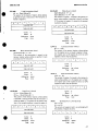
iSBC 80/10BTM
SINGLE BOARD COMPUTER
HARDWARE REFERENCE MANUAL
•
Order Number: 9803119-02
•
•
•
I
Copyright @ 1979, 1981 Intel Corporation
Intel Corporation, 3065 Bowers Avenue, Santa Clara, California 95051
r
REV.
PRINT
DATE
REVISION HISTORY
-001
Original Issue
10179
-002
Revised: Tables 1-1, 2-8, 2-10
Sections: 2-20 & 5-2
Appendix C.
4/81
I..
•
Additional copies of this manual or other Intel literature may be obtained from:
Literature Department
Intel Corporation
3065 Bowers Avenue
Santa Clara, CA 95051
The information in this document is subject to change without notice.
Intel Corporation makes no warranty of any kind with regard to this material, including, but
not limited to, the implied warranties of merchantability and fitness for a particular purpose.
Intel Corporation assumes no responsibility for any errors that may appear in this document.
Intel Corporation makes no commitment to update nor to keep current the information
contained in this document.
•
Intel Corporation assumes no responsibility for the use of any circuitry other than circuitry
embodied in an Intel product. No other circuit patent licenses are implied.
Intel software products are copyrighted by and shall remain the property of Intel
Corporation. Use, duplication or disclosure is subject to restrictions stated in Intel's software
license, or as defined in ASPR 7-104.9(a)(9).
No part of this document may be copied or reproduced in any form or by any means without
the prior written consent of Intel Corporation.
The following are trademarks of Intel Corporation and its affiliates and may be used only to
identify Intel products:
BXP
CREDIT
i
ICE
iCS
im
Insite
Intel
Intel
Intelevision
InteIlec
iRMX
iSBC
iSBX
Library Manager
MCS
Megacha88is
Micromap
Multibua
Multimodule
PROMPT
Promware
RMX/BO
System 2000
UPI
pScope
and the combination of ICE, iCS, iRMX, iSBC, iSBX, MCS, or RMX and a numerical suffix.
ii
I A353/581/5K
DO
I
•
•
•
•
PREFACE
This manual provides general information, preparation for use instructions,
programming information, principles of operation and service information for the
iSBC 80/lOB Single Board Computer. Additional related information is provided in
the following Intel documents:
•
•
•
•
•
Intel MCS-80 User's Manual, Order Number 9800153.
Intel 8080/8085 Assembly Language Programming Manual, Order Number
9800301.
Intel Multibus Specification, Order Number 9800683.
Intel iSBX Bus Specification, Order Numer 142686.
Designing iSBX Multimodule Boards, Ap. Note AP-96.
•
•
.
•
iii
CONTENTS
•
I
CHAPTER 1
GENERAL INFORMATION
PAGE
Introduction. .. . . . . . . .. .. . . . . . . .. . ..... . . . ....... 1-1
Description ........ . . . . . . . . . . . . . . . . . . . . . . . . . . . . .. 1-1
Documentation Supplied ......................... 1-2
Additional Equipment Required ................. 1-2
Specifications ................................... 1-2
CHAPTER 2
PREPARATION FOR USE
Introduction ..................................... 2-1
Unpacking and Inspection .. . .. .. .. .. . .. .. . .. ... 2-1
Installation Considerations ...................... 2-1
Minimal Operating Requirements .............. 2-1
Power Requirements ........................... 2-1
Cooling Requirements ......................... 2-2
Component Installation ......................... 2-2
ROM/PROM Installation ..................... : 2-2
RAM Installation ............................. 2-3
Line Drivers and 1I0
Terminators .................................. 2-4
Jumper Configurations .......................... 2-5
Programmable Communications
Interface Hardware
Configuration ................................ 2-7
Baud Rate Selection ......................... 2-7
Serial Interface Interrupts ................... 2-8
Conversion to RS232C Interface ............. 2-8
Serial Interface External Clock .............. 2-8
Programmable Peripheral
Interface Configurations ....................... 2-8
Optional RAM Configuration .................. 2-9
Failsafe Timer Jumper ........................ 2-9
Millisecond Timer ............................. 2-9
Connector Information .......................... 2-9
Multibus Signal Characteristics ................ 2-10
Priority Resolution ............................. 2-17
Multimodule Configuration ..................... 2-18
Power Fail and Memory
Protect Configuration ......................... 2-18
Using RMX-80 Software ........................ 2-19
SerialllO Cabling ............................. 2-19
ParallelllO Cabling ........................... 2-20
Board Installation ....... . . . . . . . . . . . . . . . . . . . . . .. 2-21
CHAPTER 3
PROGRAMMING INFORMATION
Introduction .....................................
Memory Addressing .............................
1I0 Addressing .................................
System Initialization ............................
8251A PCI Programming ........................
Mode Instruction Format ......................
iv
3-1
3-1
3-1
3-2
3-2
3-2
PAGE
Sync Characters .............................. 3-3
Command Instruction Format ................. 3-3
Reset .......................................... 3-4
Addressing .................................... 3-4
Initialization .................................. 3-4
Operation ..................................... 3-4
8255A PPI Programming ........................ 3-6
Control Word Format .......................... 3-7
Addressing .................................... 3-7
Initialization .................................. 3-7
Operation ..................................... 3-8
Port E4 ..................................... 3-8
Port E5 ..................................... 3-9
Port E6 ..................................... 3-9
Ports E8 and E9 ........ . . . . . . . . . . . . . . . . . . . .. 3-9
Port EA .................................... 3-10
•
CHAPTER 4
PRINCIPLES OF OPERATION
Introduction ... "................................. 4-1
Functional Description .......................... 4-1
Clock Circuits ................................. 4-1
Central Processing Unit Group ................ 4-1
Serial I/O Interface ........................... 4-2
Parallel I/O Interface ......................... 4-2
ROM/PROM Memory ......................... 4-2
RAM Memory ................................. 4-2
Multimodule Interface ......................... 4-2
Multibus Interface ...... . . .. . . . . . . . . . . . . . . . . . .. 4-2
Circuit Analysis ................................. 4-2
CPU Group ................................... 4-3
Instruction Timing .......................... 4-3
Interrupt Sequences ......................... 4-7
Hold Sequences ............................. 4-7
Halt Sequence ............................... 4-7
Start-Up Sequence ........................... 4-7
Read/Write Signal Generation ................. 4-8
ROM/PROM Operation ....................... 4-8
RAM Operation ............................... 4-9
I/O Operation ................................. 4-9
On-Board 1I0 Operation .................... 4-9
Off-Board 1I0 Operation .................... 4-9
SerialllO Interface ........................... 4-9
Asynchronous Mode ........................ 4-10
Synchronous Mode ......................... 4-10
SerialllO Interrupts ....................... 4-11
PPI Operation ................................ 4-11
Mqltibus Interface ............................ 4-12
Interrupt Handling ........................... 4-12
Multimodule 1I0 Board Operation ............ 4-12
•
•
•
..
•
•
CONTENTS (Continued)
CHAPTER 5
SERVICE INFORMATION
APPENDIXC
ADDRESS DECODE PROM
APPENDIX A
8080A INSTRUCTION SET
APPENDIXD
FUNCTIONAL DIFFERENCES
TABLES
TABLE
1·1
2·1
2·2
2·3
2·4
2·5
2·6
2·7
2·8
2·9
2·10
2·11
2·13
2·14
2·15
2·16
2·17
3·1
3-2
3:3
3·4
3-5
•
APPENDIXB
TELETYPEWRITER MODIFICATIONS
Introduction ..................................... 5-1
Service and Repair Assistance ................... 5-1
Replacement Parts .............................. 5-1
2·12
•
PAGE
3-6
3·7
3-8
TITLE
PAGE
Specifications .............. " . . . . . . . . . .. 1·2
Power Supply Requirements ............ 2·1
Empty I.C. Sockets ..................... 2·2
ROM/EPROM Reference Chart ......... 2·3
ROM Socket Address Ranges ........... 2·3
RAM Socket Pairs ...................... 2-4
Parallel 110 Line Identification ......... 2-4
Recommended Line Drivers
and Terminators ........................ 2·6
Jumper Configurations ................. 2·6
Baud Rate Selection .................... 2-8
User·Furnished Connector Details ...... 2·10
PI and P2 Connector
Pin Assignments ...................... 2-11
Signal Functions Used By the
iSBC 80/10B Board .................... 2·12
iSBC 80/lOB DC Characteristics ....... 2-13
AC Characteristics with
Continuous Bus Control ............... 2·15
AC Characteristics with
Bus Exchange ......................... 2-16
Pin Assignments for
Connector J3 .......................... 2-19
J3IRS232C Connector
Pin Correspondence . . . . . . . . . . . . . . . . . . .. 2-20
Memory Addressing .................... 3-1
110 Addressing ......................... 3-1
Typical PCI Mode or Command
Instruction Subroutine .................. 3-5
Typical PCI Data Character
Read Subroutine ........................ 3-5
Typical PCI Data Character
Write Subroutine ........................ 3-5
Typical PCI Status Read Subroutine .... 3-6
Parallel 110 Interface Configurations
3-7
Typical PPI Initialization Subroutine ... 3-7
TABLE
3·9
3·10
3·11
3-12
3-13
3·14
3·15
3·16
3·17
3-18
3·19
3·20
3·21
3-22
3·23
3·24
3·25
3·26
3-27
TITLE
PAGE
Port E4, Mode 0 Input Configuration ... 3-10
Port E4, Mode 0 Latched
Output Configuration .................. 3·10
Port E4, Mode 1 Strobed Input
Configuration .......................... 3·10
Port E4, Mode 1 Latched Output
Configuration ......................... 3·11
Port E4, Mode 2 Bidirectional
Configuration ......................... 3-11
Port E5, Mode 0 Input Configuration ... 3-12
Port E5, Mode 0 Latched Output
Configuration ......................... 3-12
Port E5, Mode 1 Strobed Input
Configuration ......................... 3-12
Port E5, Mode 1 Latched Output
Configuration .................. '....... 3-13
Port E6, Mode 0, 8·bit Input
Configuration ......................... 3-13
Port E6, Mode 0, 8-bit Latched
Output Configuration .................. 3-13
Port E8, Mode 0, Input Configuration .. 3-14
Port E8, Mode 0 Latched Output
Configuration ......................... 3-14
Port E9, Mode 0 Input Configuration ... 3-14
Port E9, Mode 0 Latched Output
Configuration ......................... 3-13
Port EA, Mode 0, 8-bit Input
Configuration ......................... 3-15
Port EA, Mode 0, 8-bit Latched
Output Configuration .................. 3-15
Port EA, Mode 0 Upper 4·bit InputiLower
4·bit Latched Output Configuration .... 3-15
Port EA, Mode 0 Upper 4·bit Latched
Output/Lower
4·bit Input Configuration .............. 3-15
v
ILLUSTRATIONS
FIGURE
TITLE
PAGE
1-1
iSBC 80110B Single Board
Computer ............................... 1-1
2-1
Pin Alignment .......................... 2-2
2-2
Device Type Sockets .................... 2-3
2-3
Bus Exchange Timing (Write) .......... 2-12
2-4
Memory and 1/0 Read Timing ......... 2-14
2-5
Memory and I/O Write Timing ..... . . .. 2-17
2-6
Multibus Compatible Priority
Resolution ............................. 2-18
2-7
Replacement Method Priority
Resolution ............................. 2-18
3-1
PCI Synchronous Mode Instruction
Word Format ........................... 3-2
3-2
PCI Synchronous Mode
Transmission Format ................... 3-2
3-3
PCI Asynchronous Mode Instruction
Word Format ........................... 3-3
3-4
PCI Asynchronous Mode
Transmission Format ................... 3-3
FIGURE
TITLE
PAGE
3-5
PCI Command Instruction
Word Format .......................... . 3-3
3-6
Typical PCI Initialization and
Data 1/0 Sequence .................... . 3-4
3-7
PCI Status Read Format ............... . 3-6
3-8
PPI Control Word Format .............. . 3-8
3-9
PPI Port C Bit SetlRESET
Control Word Format .................. . 3-8
4-1
iSBC 80/10B Block Diagram ........... . 4-1
4-2
Typical FETCH Machine Cycle ........ . 4-4
4-3
Input Instruction Cycle ................ . 4-5
4-4
Output Instruction Cycle ............... . 4-6
4-5
Memory and I/O Read Timing ......... . 4-8
4-6
Memory and 1/0 Write Timing ......... . 4-8
5-1
iSBC 80110B Parts Location Diagram .. . 5-5
5-2
iSBC 80/10B Jumper Post Locations ... . 5-7
5-3
iSBC 80110B Schematic Diagram ...... . 5-9
•
•
i
•
vi
•
•
CHAPTER 1
GENERAL INFORMATION
1-1. INTRODUCTION
The iSBC 80/10B Single Board Computer is a
Multibus compatible computer system on a single
printed circuit assembly (figure 1-1). The iSBC
80/10B board includes a central processing unit
(CPU), 1K bytes of static random access memory
(RAM), one serial and six programmable 8-bit I/O
ports and sockets for up to 16K bytes of read only
memory (ROM). In addition, the board is Multimodule compatible and can be equipped with battery
backup power to preserve RAM data during a power
failure.
This manual provides all the information you will
need to promptly install and set up the iSBC 801l0B
board. Programming and service information are
also provided.
1-2. DESCRIPTION
•
The iSBC 80/10B board is controlled by an Intel
BOBOA microprocessor in conjunction with an Intel
8238 system controller and bus driver. System access
is provided through the Multibus connector and an
auxiliary 60-pin connector. Direct I/O operations
are handled through the board's 48 parallel lines or
the serial 1/0 lines.
Up to 64K bytes of memory may be directly addressed
by the iSBC 80/10B board. The first 16K bytes are
reserved for on-board ROM or PROM devices, and the
next 4K bytes for on-board RAM devices. The board
may utilize low power PROM devices with a standby
mode, and low power RAM devices.
Serial I/O operation is handled by an Intel 8251A
Programmable Communications Interface (PCI)
device. On-board circuitry allows a choice of either 20
mA current loop (TTY) or RS232C serial interface.
Baud rates are jumper selected.
The iSBC 80/10B board utilizes two Intel 8255A
Programmable Peripheral Interface (PPI) devices to
control the six, 8-bit parallel 110 ports. These ports
may be configured to a variety of dedicated or general
purpose applications. Sockets are provided to
accommodate line drivers or terminators for the two
PPI devices.
J1
J2
PARALLEL 1/0
PARALLEL 1/0
•
•
P2
Fi~e
1-1. iSBC 80/10B" Single Board Computer
1-1
iSBC80/10B
General Information
A single iSBX Multimodule connector is provided
which can accommodate a variety of special purpose
modules, allowing direct access to the on-board
CPU. Multimodule boards reside directly on the
iSBC 80110B board, and do not require external
power.
layout drawing. Refer to Chapter 5 for related
information.
1-4. ADDITIONAL EQUIPMENT
REQUIRED
The iSBC 80/10B board is designed to operate as a
limited master in either the iSBC 655 System
Chassis, the iSBC 660 System Chassis, or the iCS 80
Industrial Chassis. The board may also reside in
your own custom designed chassis, using Multibus
compatible connectors (refer to Chapter 2).
The iSBC 80/l0B board requires few optional
components for operation. Depending on your
application, you may need to purchase up to three 110
connectors and cables. Anyon-board ROMIPROM
must also be purchased separately. Chapter 2
provides information for selecting these items, based
on your specific needs.
1-3. DOCUMENTATION SUPPLIED
1-5. SPECIFICATIONS
Each iSBC SOl10B board is shipped with a corresponding set of schematic diagrams and a component
Specifications of the iSBC 80/10B board are provided
in table 1-1.
Table 1-1. Specifications
CPU
Intel8080A
WORD SIZE
Address
Data
Instruction
16 bits
8 bits
8. 16. or 24 bits
CYCLE TIME
Basic Instruction Cycle - 1.95 "'s
SYSTEM CLOCK
2.048 MHz ± 0.1%
MEMORY ADDRESSING
(factory configuration)
On-Board ROM/EPROM
On-Board RAM
O-OFFF (see section 2-8)
3COO-3FFF (see section 2-9)
MEMORY CAPACITY
On-Board ROM/EPROM
On-Board RAM
Off-Board Expansion
16K bytes (sockets only)
4K bytes
Up to 64K bytes using user specified combinations of RAM. ROM. and EPROM.
8255A No.2
Port
A
a
C
A
a
Address
E4
E5
E6
E8 E9 EA
C
8255A 8255A
No.1
No.2
8251A 8251A
Control Control Data Control
E7
EB
1/0 CAPACITY
1-2
..
•
.
On-Board Programmable 1/0
Parallel
Serial
I.
•
1/0 ADDRESSING
8255A No.1
•
48 programmable lines
1;ransmit. 1 receive
EC
ED
Isax
Isax
Multlmodule
MCSO
Multlmodule
MCS1
FO-F7
F8-FF
General Information
iSBC80/10B
•
•
•
Table 1-1. Specifications (Cont'd)
SERIAL BAUD RATES
Frequency (kHz)
(Jumper Selectable)
SERIAL COMMUNICATION
CHARACTERISTICS
Synchronous
Asynchronous
(Program Selectable)
Synchronous
-
307.2
153.6
76.8
38.4
19.2
9.6
6.98
4.8
-
38400
19200
9600
6960
4800
+ 16
+ 64
19200
9600
4800
2400
1200
600
4800
2400
1200
600
300
300
150
110
75
5-8 bit characters; internal or external character synchronization; automatic sync
insertion
Asynchronous
5-8 bit characters; break character generation; 1, 1Y2, or 2 stop bits; false start bit
detectors
Interrupts
Single-level with on-board logic that automatically vectors processor to location
38 (hex) using a restart instruction (RESTART 7). Interrupt requests may originate from user specified I/O (2); the programmable peripheral interface (2); Multimodule board (2); or the programmable communications interface (2).
MILLISECOND TIMER
INTERFACES
Multibus Lines
Parallel I/O
Serial I/O
Interrupt Requests
Multimodule Board (iSBX)
PHYSICAL CHARACTERISTICS
•
Baud Rate (Hz)
LINE DRIVERS
AND TERMINATORS
I/O Drivers
Period 1.432 ms ± 0.1% with jumper 8D-81 installed.
Period 2.084 ms ± 0.1% with jumper 8D-81 removed
All signals TTL compatible (P1 & P2)
All signals TTL compatible (J1 & J2)
RS232C or a 20 mA current loop TTY interface (jumper selectable) (J3)
All TTL compatible (active-low)
(J4)
Width - 12.00 in. (30.48 cm)
Length - 6.75 in. (17.15 cm)
Thickness - 0.50 in. (1.27 cm)
Weight - 14 oz. (484.4 gm)
The following line drivers and terminators are all compatible with the I/O driver
sockets on the iSBC 80/10B board:
Driver
Characteristic
Sink Current (mA)
7438
7437
7432.
7426
7409
7408
7403
7400
I,OC
I
NI
I,OC
NI,OC
NI
I,OC
I
48
48
16
16
16
16
16
16
NOTE
I
•
= inverting;
NI
= non-inverting; OC = open collector.
Port E4 has 28 mA totem pole drivers and 1 kO terminators .
I/O Terminators
2200/3300 divider or 1 kO pullup
1-3
General Information
iSBC80/10B
Table 1-1. Specifications (Cont'd)
BUS DRIVERS
Function
Characteristic
Sink Current (mA)
Data
Address
Commands
Tri-state
Tri-state
Tri-state
32
34
32
•
i
I
"
ENVIRONMENTAL
CHARACTERISTICS
Operating Temperature
ELECTRICAL
CHARACTERISTICS
2732 EPROM!
Power Down Requirements
(RAM & Support Circuit)
3.1A
3.46A
200 mA/K (2114)
100 = 150 mA
400 mA
150 mA
Not Required
Vee - 5V ±5%
leB = 2 mA
200 mA
2 mA
Not Required
VAA -12V ±5%
1M = 175 mA
175 mA
175 mA
Not Required
Voltage
Without EPROM1
WIth 2708 EPROM2
Vee +5V ±5%
14ee = 2.0A
Voo +12V ±5%
With 2758, 2716
NOTES:
1. Does not include power required for optional ROMIEPROM, 1/0 drivers or 1/0 terminators.
2. With four Intel 2708 EPROMS and 220/330 for terminators, instal.ied for 40 input lines. All
terminator inputs low.
3. Same as #2 except with four 2758 or 2716 or 2732 installed.
4. Icc shown without RAM supply current. For 2114 add .2A per K byte to a maximum of .8 amps
for 4K.
•
•
•
•
I
1-4
•
•
•
CHAPTER 2
PREPARATION FOR USE
2-1. INTRODUCTION
2-3. INSTALLATION CONSIDERATIONS
This chapter provides specific information enabling
you to install the iSBC 80110B board into your
system, with minimal effort. The board's default, or
factory configuration for RAM addressing, ROM
type, and other variables is described, followed by
procedures for altering the default configuration. In
this manner, the board will accommodate a variety of
applications. To completely familiarize yourself
with the flexibility of the iSBC 80/10B board, we
recommend reading the entire chapter before
installation and use.
There are several general requirements which should
be considered, prior to board installation. These
requirements are discussed in sections 2-4 through
2-6.
2-2. UNPACKING AND INSPECTION
Inspect the shipping carton immediately upon receipt
for evidence of mishandling during transit. If the
shipping carton is severely damaged or waterstained,
request that the carrier's agent be present when the
carton is opened. If the carrier's agent is not present
when the carton is opened and the contents of the
carton are damaged, keep the carton and packing
material for the agent's inspection.
For repairs to a product damaged in shipment contact
the Intel Technical Support Center (see section 5-2) to
obtain a Return Authorization Number and further
instructions. A purchase order will be required to
complete the repair. A copy of the purchase order
should be submitted to the carrier with your claim.
•
The iSBC 80/lOB board standard configuration is
described in Chapter 1. In order to operate the board
you will need additional equipment. For most
applications this will typically be the following:
a.
b.
c.
d.
CPU software, residing in on-board ROM
(section 2-8).
I/O connectors and cables (section 2-21).
Additional on-board RAM, if more than 1K bytes
are required (section 2-9).
Line dri vera or terminators for parallel I/O ports
(section 2-10).
Instructions for installing these components are
given in this chapter.
2-5. POWER REQUIREMENTS
Four voltages are required for operating the iSBC
80/lOB board: +5 Vdc, -5 Vdc, +12 Vdc, and -12
Vdc. All must be within ±5.0% of absolute. Power
requirements for the various board configurations
are listed in table 2-1.
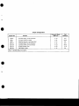
Table 2-1. Power Supply Requirements
Voltage
Without EPROM'
With 2708 EPROM'
With 2758, 2716
2732 EPROM3
Power Down Requirements
(RAM & Support Circuit)
Vcx;+5V±5%
14cx; = 2.0A
3.1A
3.46A
200 mA/K (2114)
400 mA
150 mA
Not Required
Voo +12V ±5%
•
2-4. MINIMAL OPERATING
REQUIREMENTS
100
= 150 mA
VBB - 5V ±5%
IBB= 2 mA
200 mA
2mA
Not Required
VAA -12V ±5%
1M = 175 mA
175 mA
175mA
Not Required
NOTES:
1. Does not include power required for optional ROM/EPROM, I/O drivers or I/O terminators.
2. With four Intel 2708 EPROMS and 220/330 for terminators, installed for 40 input lines. All terminator inputs low.
3. Same as #2 except with four 2758 or 2716 or 2732 installed.
4. Icc shown without RAM supply current. For 2114 add .2A per K byte to a maximum of .8 amps for 4K.
2-1
iSBC80/10B
Preparation for Use
2-6. COOLING REQUIREMENTS
socket. The following cautions are suggested:
Operating temperature range for the iSBC 80110B
board is 0° to 55° Celsius. If the board is installed
into an iSBC 655 or iSBC 660 System Chassis, or an
iCS Industrial Chassis, adequate cooling is provided
by the supplied fans. However, if the board is used in
another chassis, ensure adequate cooling is provided
by taking temperature readings inside the chassis, at
the site environment.
a.
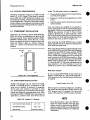
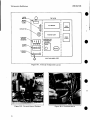
2-7. COMPONENT INSTALLATION
Instructions for installing optional ROM/EPROM,
RAM, line drivers or terminators are given in the
following sections. When installing optional ROMI
EPROM or RAM devices, ensure that pin 1 of the
device corresponds to the pin 1 marking on the board
(white dot). Refer to figure 2-1. Table 2-2 lists all
empty I.C. sockets, and identifies their intended
function.
WHITE DOT
\
/-
~
0
0
0
0
0
0
PIN 1
0
0
0
DEVICE
SOCKET
0
0
0
0
Once your devices are installed, it is necessary to
install header plug P3 into the corresponding device
type socket. There are two sockets used for ROMI
EPROM type selection: J6 and J7. Each of these
sockets is divided into an upper half and a lower
half. Plug P3 must be placed in one of the four halves
(refer to table 2-3). Each half of sockets J6 and J7 are
labeled on the board, as shown in figure 2-2.
After selecting the ROM/EPROM type, another
header plug (P4) must be configured to indicate power
down mode and access time.
When using devices with a low power standby mode,
such as the Intel 2716 or 2732 PROM, the P4 plug may
be placed into the PWR DN (upper) position, if ROM
access is less than or equal to 350 ns. When using
2708 or ROMs with greater than 356 ns access P4
must be placed in the NORM (lower) position. When
your application does not require anyon-board ROM,
header plug P3 should not be inserted hito J6 or
J7. Since the iSBC 80110B board is shipped with the
plug installed in the 2708 position, it would be
necessary to remove it if no on-board ROM is used.
NOTCH
r.::~
Never install any device into a live board, that is,
one with power applied.
b. Ensure pin 1 of the device is aligned to pin 1 of the
socket.
c. Insert the device slowly; check all pins to ensure
correct insertion.
0
0
0
0
0
0
•
•
•
Wait State Jumper
PSJ24
Figure 2-1. Pin Alignment
If you are using ROM/PROM devices which have
. memory access times of > 550 nanoseconds and <
1020 nanoseconds, the following jumper modification
is required:
2-8. ROM/EPROM INSTALLATION
Sockets U19 through U22 are reserved for ROM,
PROM, or EPROM devices. A maximum of 16K
bytes may be installed. A summary of compatible
device types, and capacity is provided in table
2-3. Device types may not be mixed, however empty
sockets are allowed (in ascending order only). After
selecting the ROM or EPROM which best suits your
application, carefully insert each device into its
Table 2-2. Empty I.C. Sockets
Line DriverlTerminator Sockets
U2 - U11
ROM/EPROM Sockets
U1!t- U22
RAM Sockets
2-2
U34-36 and U38-40
Install jumper 108 to 109
Refer to figure 5-3, sheet 4 and figure 5-2. Installing
this jumper imposes mandatory WAIT states on all
CPU memory and 110 requests. The board will
realize a 25% speed loss with this jumper installed.
NOTE
Some Multimodules require the MWAITI
signal for proper operation. The wait state
jumper cannot be used when the MWAITI
signal is required. Refer to your Multimodule
Hardware Reference Manual for additional
information.
•
Preparation for Use
iSBC80/lOB
•
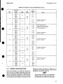
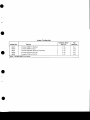
Table 2-3. ROM/EPROM Reference Chart
EPROM1
Type
ROM1
Type
Capacity
Header Plug
P3
Max ROM Address
(Hexadecimal)
2708
26082
1K x 8
J6 Lower
OFFF
2758
-
1K x 8
J6 Upper
OFFF
2716
2316E
2K x 8
J7 Upper
1FFF
2732
2332A
4K x 8
J7 Lower
3FFF
NOTES:
1. Refer to the Intel Component Data Catalog for device specifications.
2. Factory Programmable PROM.
•
Summary of the ROM
installation procedure:
J6
a.
b.
J7
2716
2758
c.
•
Install devices into sockets UI9 through U22.
Configure board to correct device type, using
header plug P3.
Select correct device access time using header
plug P4.
The base or starting address of the ROM area is 0000
(Hexadecimal). The upper or maximum address of
the ROM area will naturally depend on the type of
devices installed. These values are provided in table
2-3. This scheme assumes that a device is residing in
each of the four ROM sockets. You do not necessarily
have to install a device into each socket, providing
the empty sockets are not addressed. The upper
address of each socket is provided in table 2-4.
P3
2-9. RAM INSTALLATION
2708
2732
There are three important concepts to be considered
when installing optional RAM devices:
Note: Shown with P3 in 2708 position.
•
PSI25
a.
b.
c.
Figure 2-2. Device Type Sockets
RAM devices must always be installed in pairs;
Device placement determines address spacing;
Amount of ROM/EPROM installed determines
RAM starting address.
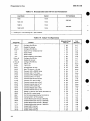
Table 2-4. ROM Socket Address Ranges (Hexadecimal)
•
Device Type
U19
U20
U21
U22
1K x 8
0- 03FF
0400 - 07FF
0800 - OBFF
OCOO - OFFF
2K x 8
0- 07FF
0800 - OFFF
11000 - 17FF
1800 - 1FFF
4K x 8
0- OFFF
1000 -1 FFF
2000 - 2FFF
3000 - 3FFF
2·3
Preparation for Use
iSBC80/10B
The iSBC 80/l0B board is shipped with lK bytes of
RAM residing in sockets U37 and U41. In this
standard configuration the base address is 3COO
(Hex) when lK or 2K ROM devices are installed. If
4K ROM devices are installed, the base address is
4COO (Hex).
Additional RAM devices may be installed in lK byte
increments, with the base address being reduced
accordingly (table 2-5). With the full 4K bytes of
RAM, its space would cover 3000 to 3FFF with lK or
2K ROM devices installed, or 4000 to 4FFF with 4K
ROM devices installed.
Notice that with the lK or 2K ROM devices installed,
a memory gap will exist from the end of ROM space to
the beginning of RAM space. More precisely, with
the lK ROM devices installed, the gap will be from
1000 to 2FFF, and with 2K ROM devices installed the
gap will be from 2000 to 2FFF. If your application
requires that you assign any of these addresses to
memory, it will, of course, need to be off-board.
If installing additional RAM to the standard lK byte
configuration, the following jumper modification
must be performed (refer to figure 5-2):
Install jumper 96 to 97
•
This modification indicates (to the CPU) that there
are 2K to 4K bytes of RAM on-board. Without the
jumper, as in the factory default configuration, lK
bytes are indicated.
2-10. LINE DRIVERS AND
I/O TERMINATORS
Line drivers or I/O terminators may be installed in
sockets U3 through Ull. These sockets correspond to
the 48 parallel I/O lines available on the iSBC
8O/lOB board. Table 2-6 identifies these lines and
their corresponding ports. For additional information, refer to figure 5-3, sheets 7 and 8. Table 2-7 lists
the types of I/O terminators and line drivers which
are recommended for use with the iSBC 80/l0B
board. Notice that two driver or terminator devices
are required for one port.
.
•
Table 2-5. RAM Socket Pairs
I
,
Sockets
Addresses'
Pair 0
U37, U41
xcoo- XFFF
Pair 1
U36, U40
xaoo - XBFF
Pair 2
U35, U39
X400 - X7FF
Pair 3
U34, U3a
XOOO - X3FF
•
!
i
Note:
1. X prefix will be 3 with 1K or 2K ROM devices; and 4 with 4K ROM devices installed.
•
Table 2-6. Parallel I/O Line Identification
1/0
Port
E4
2-4
Component
Line
Function
Data
Data
Data
Data
Data
Data
Data
Data
0
1
2
3
4
5
6
7
1/0
Socket
U1
U1
U1
U1
U1
U1
U1
U1
PPI
Device
U16
Port
A
1/0
Connector
Pin
Jl-43
Jl-41
Jl-45
Jl-47
J1-39
J1-37
J1-35
J1-33
"
Notes:
Bus Transceiver is factory
installed for this port
(in socket U1).
Schematic reference on
figure 5-3, sheet 7.
iSBC80/10B
•
Preparation for Use
Table 2-6. Parallel I/O Line Identification (Cont.)
1/0
Port
Component
Line
Function
Data
Data
Data
Data
0
1
2
3
Data
Data
Data
Data
4
5
6
7
Data
Data
Data
Data
7
5
1
0
Data
Data
Data
Data
4
6
2
3
Data
Data
Data
Data
0
1
2
3
Data
Data
Data
Data
4
5
6
7
Data
Data
Data
Data
0
1
2
3
Data
Data
Data
Data
4
5
6
7
Data
Data
Data
Data
0
1
2
3
Data
Data
Data
Data
4
5
6
7
1/0
Socket
PPI
Device
U5
U16
Port
•
•
U4
U2
•
U16
Port
113
U6
E8
U17
Port
A
J1-9
J 1-11
J1-13
J1-15
Schematic reference on
figure 5-a, sheet 7
J1-31
J1-27
J1-29
J1-25
Table indicates factory
configuration. Data lines may
be altered. Refer to section
2-17 for instructions.
J1-21
J1-23
J1-19
J1-17
Schematic reference on
figure 5-:3, sheet 7
J2-43
J2-45
J2-47
J2-49
Schematllc reference on
figure 5-:3, sheet 8
J2-41
J2-39
J2-37
J2-35
U7
U11
U17
Port
J2-5
J2-7
J2-9
J2-3
Schematic reference on
fi g u re 5-:3, sheet 8
B
J2-11
J2-13
J2-15
J2-17
U10
U9
U17
Port
J2-25
J2-23
J2-21
J2-19
Schematic reference on
figure 5-:3, sheet 8
C
EA
U8
2-11. JUMPER CONFIGURATIONS
•
J1-7
J1-5
J1-3
J1-1
C
E6
E9
•
Notes:
B
E5
•
1/0
Connector
Pin
Much of the flexibility of your iSBC 80/l0B board is
due to the use of jumper connections which may
easily be altered from their factory configurations to
suit your particular application. The following
sections describe all the jumper connections relevant
to the scope of this discussion. Locations of the
J2-27
J2-29
J2-31
J2-33
referenced jumpers are shown in figure 5-2. A
complete list of the jumpers with a brief functional
description is provided in table 2-8.
NOTE
Jumper posts are shown on the schematic
diagrams with an E prefix (e.g., E86). However, the prefix is not used on the board itself.
2-5
iSBC80/10B
Preparation for Use
•
Table 2-7. Recommended Line Drivers and Terminators
Une Drivers
Current
7400 I
16 mA
74031,OC
16 mA
7408 NI
16 mA
1/0 Terminator.
iS8C 901
..
iS8C 902
16mA
7409NI,OC
to
I
= inverting;
NI
= non-inverting;
OC
= open collector.
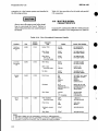
Table 2-8. Jumper Configurations
Jumper Pair
Schematic Sheet!
Grid Loc.
Text
Reference
1 thru 4
Configure Port E6 bits
7
B5
2-17
5-10*
6 thru 9
Disable E6 interrupt
Configure Port E6 bits
7 85
7 B5
7 C4
7 C4
2-17
2-17
11-X
12-X
14-X
15-X
16 thru 19
20-25'
21 thru 24
26-27*
27-28
30-31 *
32-33*
Enable CTI for millisecond timer
Enable PFSNI
Enable PFSRI
Enable millisecond timer (MST)
Configure Port E6 bits
Disable E6 interrupt
Configure Port E6 bits
GND to J2-1
+5V to J2-1
Connects RTSI to CTSI
Sets CTS driver to +12 volts
7
7
7
7
7
C4
B4
B5
85
85
8 82
8 82
6 A4
6 A4
2-20
None
2-28
None
None
34-35
Connects TxD to RS232C driver
6 84
2-15
Connects TxD to TTY driver
6
84
6 84
6 84
6 85
None
2-15
41-46*
Connects TTY return to RxD
6
85
None
42-47*
43-48*
44-49*
Connects internal clock to RxC
Connects internal clock to TxC
Connects DTR to DSA input
45-46
48-49
50-54*
59-60'
60-61
63-64'
Connects RS232C data to AxD
Connects external clock to TxC
Selects 110 baud for PCI device (see table 2-9)
Sets Port E4 to output mode
Port E4 mode programmed by Port E6 Bit 6
Connects HALT I to P2 Connector
6
6
6
6
6
85
85
B5
85
B5
D4
C5
C5
A4
None
None
None
2-15
2-16
2-13
2-17
2-17
67-68
68-69'
70-71
Enables Multimodule interrupt 0 (MINTAO)
Disables Multimodule interrupt 0 (MINTRO)
Enables Multimodule interrupt 1 (MINTA1)
Disables Multimodule interrupt 1 (MINTR1)
Enable RxADY interrupt
Disable AxADY interr~pt
Disable TxADY interrupt
Connects DTR to RS232C driver
Connects DTR to TTY driver
Connects external clock to RxC
6
7
7
4
8 A6
8 A6
8 A6
8 A6
6 C4
6 C4
6 84
•
2-25
2-25
2-20
2-17
2-17
2-17
35-36*
37-38
38-39*
41-42
71-72'
73-74
74-75'
76-78'
2-6
Function
None
2-16
•
..
2-21
2-24
2-24
2-24
2-24
2-14
2-14
2-14
•
Preparation for Use
iSBCSO/IOB
•
Table 2-8. Jumper Configurations (Cont'd)
Jumper Pair
Function
78-79
77-78
Enable TxROY interrupt
Enable TxE interrupt
80-81 '
82-83"
84-85"
85-86
87-88"
88-89
•
Connects AACKI to board
92-93'
94-95"
Connects BCLKI to Multibus
96-97
98-99"
100-101 "
103-104'
106-107"
108-109
W3
•
Connects INTRO to CPU INT
Connects PFINI to CPU INT
90-91
W1
W2
•
Selects 110 baud for PCI device (see table 2-9)
Connects RESET to Multibus
Connects BPRN to board
Implements BPRNI (Multi bus compatible)
Text
Reference
6 B4
6 B4
6 D4
2-14
2-14
2-13
2 C6
2 C6
2-21
2-23
2
2
2
4
C6
07
07
2-23
2-21
2-25
B7
None
3 A3
3 A3
4 C7
Connects CCLKI to Multibus
Specifies amount of on-board RAM
Reserved
Connects WAITI to P2 Connector
5
4
4
4
Connects SYNC to P2 Connector
Enables failsafe timer
Wait State Jumper
-12V to J3-19
2-21
2-21
2-9
B6
A2
None
2-21
C3
B4
None
2-19
2-8
A7
B2
6 A7
6 C6
4
6
GNO to J3-1
+12V to J3-22
2-27
None
2-28
Note: ' indicates default connection
2-12. PROGRAMMABLE COMMUNICATIONS
INTERFACE HARDWARE
CONFIGURATION
All serial data I/O operations are controlled by the
Programmable Communications Interface (PCI)
device (U18). Several hardware features of the PCI
can be reconfigured, to match your application. The
following features may be reconfigured:
a.
b.
c.
d.
e.
Baud rate;
Interrupt request mechanism;
Interface type;
Transmit and Receive Clock source;
Control line configuration.
The iSBC SO/lOB board is shipped in the following
configuration:
•
Schematic Sheetl
Grid Loc.
a.
b.
c.
d.
e.
Baud rate set to 110.
Interrupt not connected to CPU.
TrY (20 rnA current loop) interface.
Internal Transmit and Receive clock connected.
RTS looped to CTS; DSR jumper installed.
The following sections give procedures for reconfiguring of the listed features.
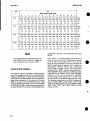
2-13. BAUD RATE SELECTION. When shipped,
the iSBC 80/10B board is configured for 110
baud. This rate may be reconfigured to another
value, as shown in table 2-S. Physically, it will be
necessary to remove the existing jumpers and then to
install the jumper indicated in the table. Location of
the jumpers on the board is shown in figure
5-2. Schematically, the jumper connections are
shown in figure 5-3, sheet 6.
Notice that the baud rate is derived by hardware
jumper placement and a software selected divide
rate. The software baud rate factor is sent from the
CPU to the PCI as part of the Mode Instruction
Format byte. This procedure is described in Chapter
4.
A baud rate of 9600 may be obtained only
with a divide factor of 16. See table 2-9.
2-7
Preparation for Use
iSBCSO/I0B
Table 2-9. Baud Rate Selection
•
Effective Baud Rate (Hz)
Synchronous Mode
Jumper'
Connection
57-50
56-50
55-50
51-50
52-50
53-50
54-50
54-50
80-81
Asynchronous Mode
Software
Baud Rate Factor = 16
(see note 2)
-
19,200
96003
4800
2400
1200
600
300
38,400
19,200
9600
4800
-
6980
Software
Baud Rate Factor
(see note 2)
= 64
4800
2400
1200
600
300
150
75
110 (TTY)
Note:
1. If jumper pair 80-81 is not connected, the frequency at jumper pole 54 is 4.8 KHZ. If jumper 80-81 is connected, however,
the frequency at jumper pole 54 is 6.98 KHZ which, with a programmed baud rate factor of 64, provides an effective baud
rate of approximately 110 baud for Teletype use.
2. Baud rate factor is software selectable, within above limits.
3. Caution: Baud Rate Factor = 16.
4. Jumper 58 not recommended for-PCI use.
2-14. SERIAL INTERFACE INTERRUPTS. As
shipped from the factory, the iSBC 80/10B board's
PCI circuitry will not interrupt the CPU. Rather, its
status will be read in a polled fashion, as directed by
the CPU program. The board may be reconfigured to
allow the PCI device to interrupt the CPU. The
following list describes the three different interrupt
mechanisms allowed, and indicates how to implement each type.
a.
b.
c.
Receiver Ready Interrupt. Remove jumper 74 to
75; install jumper 74 to 73.
Transmitter Ready Interrupt. Remove jumper 76
to 78; install jumper 78 to 79.
Transmitter Empty Interrupt. Remove jumper 76
to 78; install jumper 78 to 77.
c.
If your application requires the use of external
transmit and receive clocks in the RS232C mode, refer
to section 2-16.
2-15. CONVERSION TO RS232C INTERFACE. The iSBC 80110B board is shipped with the
serial interface channel configured to the TTY (20 rnA
current loop) mode. To convert this to the RS232C
mode, the following modifications must be performed:
a.
b.
2-8
Remove jumper 35 to 36; install jumper 35 to 34.
Remove jumper 38 to 39; install jumper 38 to 37.
•
Figure 5-2, zone C4, gives the physical location of the
relevant jumper posts. They are also shown schematically in figure 5-3, sheet 6.
2-16. SERIAL INTERFACE EXTERNAL
CLOCK. In the standard configuration, the transmit and receive clocks (TxC and RxC) are driven by
the on-board timer network. To use external clock
sources for TxC and RxC, the following modifications
are required:
a.
Figure 5-2, gives the physical location of the relevant
jumper posts. They are also shown schematically in
figure 5-3, sheet 6, zone C4.
Remove jumper 46 to 41; install jumper 46 to 45.
•
b.
For TxC: remove jumpers 43 to 48 and 44 to 49;
install jumper 48 to 49.
For RxC: remove jumpers 42 to 47 and 41 to 46;
install jumper 41 to 42.
•
Figure 5-2, zone C3, gives the physical location of the
relevant jumper posts. They are also shown schematically in figure 5-3, sheet 6, zone C5.
2-17. PROGRAMMABLE PERIPHERAL
INTERFACE CONFIGURATIONS
The iSBC SO/lOB board utilizes two Intel 8255A
•
Preparation for Use
iSBC80/10B
•
Programmable Peripheral Interface (PPI) devices to
control the board's six 8-bit I/O ports. Three ports
are interfaced through connector Jl and three are
interfaced through connector J2. Table 2-6 provides
port and line identification of the two PPI devices.
Since each port may be programmed to suit several
applications, specific information pertaining to the
use of each port is provided in Chapter 3. Using one
port in a particular mode may impose restrictions on
another port. There are also certain jumper connections which are required for certain applications.
Refer to sections 3-13 through 3-22 forcompletePPI
programming instructions and jumper requirements.
•
•
•
Lines which are used as outputs will require line
driver circuits for proper operation. Likewise, lines
which are used as inputs require terminator
networks. Recommended line/driver and terminator devices are provided in table 2-7.
Unlike the other PPI ports, each bit of port E6 is
jumper connected to its driver/terminator socket pin
(U2, U3). This allows greater flexibility for port
configurations when using the on-board millisecond
timer (section 2-20), a power-fail configuration
(section 2-25) or an interrupt (section 3-20). The
jumper can also be used to reconfigure the bit order of
port E6.
The iSBC 80/10B board is equipped with an on-board
failsafe timer. This timer is activated at the beginnig
of every CPU machine cycle. If an acknowledge is
not received within approximately 10 milliseconds,
the failsafe timer expires, and issues an acknowledge
signal, so the CPU may resume operation. If your
application does not require this feature, the
following modification must be performed:
Remove jumper 106 to 107
Figure 5-2, zone C7, gives the physical location of the
relevant jumper posts. They are also shown schematically in figure 5-3, sheet 4, grid location B4.
2-20. MILLISECOND TIMER
A millisecond timer may be implemented on-board
for use as a reference period. This timer does not
affect the baud rate clock or the failsafe timer. The
period of the millisecond timer, however, is affected
by the l10 baud jumper 80-81 (Fig. 5-3, Sheet 6). With
80-81 installed, the timer signal is low for 0.7ms
(l.4ms period). With 80-81 removed, the timer signal
is low for 1.0ms (2.0ms period). The timer may be
reset at any time by CTI, but if it is not reset it will
continue as a symmetrical signal with the period
described above. To implement the millisecond
timer:
Port E4 is default configured to the output mode, with
a bus transceiver installed in socket Ul. Alternatively, the bus transceiver mode (input or output) can
be specified under program control by performing the
following modifications:
a.
a.
Remove jumper 59 to 60.
b.
b.
Install jumper 60 to 6l.
Port E6, bit 6 (PPI port C6) will then determine input
mode or the output mode. Refer to section 3-18 for
port C programming information.
To place the transciever in the input only mode,
remove jumper 59-60.
2-18. OPTIONAL RAM CONFIGURATION
If you install additional RAM devices on-board, the
following jumper modification is required for proper
memory addressing:
Install a jumper from timer output (post E15) to
the appropriate location. For example, timer
output may be connected to an 8255A port E6
input line, a port E6 output driver, or it may be
used as an interrupt source. Refer to Figure 5-3,
Sheet 7, zone C4.
'
Install a jumper from CTI (post Ell) to the
appropriate location which will control resetting
the timer. For example, CTI may be connected to
an 8255A port E6 output line, a port E6 input
terminator, or it may be tied low. Refer to Figure
5-2, Sheet 7, zone C4 .
The output of the timer may be verified at jumper
post 15. The clock output is generated at U27, pin 13
and is identified as MST (Millisecond Timer). Refer
to Figure 5-3, Sheet 6, zone C2. Jumper posts are
located between sockets U2 and U3 on the board.
2-21. CONNECTOR INFORMATION
This modification indicates more than lK bytes of
RAM reside on-board.
For systems applications, the iSBC BO/lOB board is
designed for installation into a standard Intel iSBC
604 or iSBC 614 Cardcage and Backplane assembly.
Alternatively, the board may be interfaced with a
design of your own choice, by means of an 86-pin
connector. Refer to table 2-10 for a list of suggested
manufacturers.
This jumper is shown on figure 5-2, and schematically on figure 5-3, sheet 4, zone C7.
Multibus signal characteristics and methods of
implementing a priority resolution scheme for bus
Install jumper 96 to 97.
•
2-19. FAILSAFE TIMER JUMPER
2-9
iSBC80/10B
Preparation for Use
contention in a dual master system are described in
the following sections.
Table 2-10 also provides a list of serial and parallel
I/O connectors.
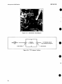
2-22. MUL TIBUS SIGNAL
Always turn off system power before installing or removing the board. Failure to
observe this precaution can cause damage to
the board.
•
CHARACTERISTICS
Connector PI interfaces the iSBC 80/lOB board to the
Multibus connector. Pin assignments are listed in
•
Table 2-10. User Furnished Connector Details
Function
Pins
Centers
(Inches)
Multibus
Connector
P1
43/86
0.156
Auxiliary
Connector
P2
Parallel
Port
Serial
Port
30/60
35/50
13/26
0.100
0.100
0.100
Connector
Type
Vendor
Vendor Part Number
Solder PCB
ELFAB
VIKING
BS 1562043PBB
2KH43/9AMK12
Wire Wrap
(no ears)
EDAC
ELFAB
337-086-0540-201
BW1562D-43PBB
Wire Wrap
(with 0.128
mounting holes)
EDAC
ELFAB
337-086-540-202
BW1562A-43PBB
Wire Wrap
EDAC
ELFAB
345-060-524-802
BS1020A-30PBB
With 0.128
mounting holes
TI
VIKING
H421121-30
3KH30/9JNK
No Ears
EDAC
ELFAB
345-060-540-201
BW1020D-30PBB
Flat Crimp
3M
3M
AMP
ANSLEY
SAE
3415-0001 (w/o ears)
3415-0000 (w/ears)
88083-1
609-5015
S06750 Series
Soldered
GTE
MASTERITE
MICROPLASTICS
VIKING
6AD01-25-1A1-DD
NDD8GR25-DR-H-X
MP-0100-25-DP-1
3KH25/9JN5
Wire Wrap
VIKING
TI
ITT CANNON
3KH25/JND5
H421011-25
EC4A050A1A
PCB Soldered
mounting holes
AMP
EDAC
1-583715-1
345-026-520-202
Flat Crimp
3M
AMP
3462-0001
88373-5
Soldered, pierced
tail
EDAC
345-026-500-201
Wire Wrap
EDAC
345-026-540-201
•
•
•
i
I
Notes:
1. Connector heights are not guaranteed to conform to OEM equipment.
2. Wire wrap pin lengths are not guaranteed to conform to OEM equipment.
3. Connector numbering convention may not agree with board connector.
2-10
,
•
iSBCBO/lOB
•
Preparation for Use
table 2-11 and descriptions of the signal functions are
provided in table 2·12.
The DC characteristics of the iSBC 80110B board
MuItibus interface signals are provided in table
2-13. The AC characteristics with continuous bus
control, are provided in table 2-14. AC characteris·
tics with bus exchange are provided in table
2-15. Bus exchange timing is shown in figure
2-3. Memory and I/O read timing is shown in figure
2-4 and memory and I/O write timing is shown in
figure 2-5.
Table 2-11. PI and P2 Connector Pin Assignments
P1 Pin Assignments
.
•
•
Signal
Function
1
GND
2
3
GND
(
Pin'
9
10
+5V
+5V
+5V
+5V
+12V
+12V
-5V
-5V
4
5
6
7
8
I
>
Power Input
I
11
GND
GND
13
14
BCLK/
INIT/
System Initialize
15
BPRN/
Bus Priority In
17
19
BUSY/
Bus Busy
MRDC/
Memory Read Command
20
21
22
MWTCI
Memory Write Command
10RC/
10WC/
XACK/
AACKI
CCLKI
INTA/
INT1/
1/0 Read Command
23
25
33
42
}
Ground
Bus Clock
I/O Write Command
Transfer Acknowledge
Advanced Acknowledge
Constant Clock
Interrupt Acknowledge
Interrupt request on level 1
P2 Pin Assignments
Pin'
Signal
Function
3
4
+5Vdc
+5Vdc
Power
13
PFSRI
PFSNI
Power Fail Sense Return
17
19
•
I
12
31
•
Ground
Power
Power Fail Sense
PFIN/
Power Fail Interrupt
Memory Protect
20
MPRO/
28
HALT/
29
WAITI
32
38
SYNC/
AUX RESET/
Auxiliary Reset
Note: All other P2 pins are reserved for future use by Intel.
• All odd-numbered pins (1, 3, 5 ... 85) are on component side of the board. Pin 1 is the left-most pin when viewed from the
component side of the board with the extractors at the top. All unassigned pins are reserved.
2·11
iSBCSO/IOB
Preparation for Use
Table 2-12. Signal Functions Used By the iSBC 80/10BTM Board
Functional Description
Signal
ADRO/-ADRF/
Address. These 16 lines transmit the address of the memory location or I/O port to be accessed.
ADRF/ is the most-significant bit.
BCLK/
Bus Clock. Used to synchronize the bus contention logic on all bus masters. When generated by the
iSBC 80/30, BCLK/ has a period of 108 nanoseconds (9.22MHz) with a 35-65 percent duty cycle.
BPRN
Bus Priority In. Indicates to a particular bus master that no higher priority bus master is requesting
use of the bus.
BUSY/
Bus Busy. Indicates that the bus is in use and prevents all other bus masters from gaining control of
the bus. BUSY/ is synchronized with BCLK/.
CCLK/
Constant Clock. Provides a clock signal of constant frequency for use by other system modules.
When generated by the iSBC 80/10B board, CCLK/ has a period of 108 nanoseconds (9.22 MHz)
with a 35-65 percent duty cycle.
DATO/-DAT7/
Data. These eight bidirectional data lines transmit and receive data to and from the addressed
memory location or I/O port. DAT7I is the most-significant bit.
INIT/
Initialization. Resets the entire system to a known internal state.
10RC/
I/O Read Command. Indicates that the address of an I/O port is on the Multibus address lines and
that the output of that port is to be read (placed) onto the Multibus data lines.
10WC/
I/O Write Command. Indicates that the address of an I/O port is on the Multibus address lines and
that the contents on the Multibus data lines are to be accepted by the addressed port.
MRDC/
Memory Read Command. Indicates that the address of a memory location is on the Multibus address
lines and that the contents of that location are to be read (placed) on the Multibus data lines .
MWTC/
Memory Write Command. Indicates that the address of a memory location is on the Multibusaddress
lines and that the contents on the Multibus data lines are to be written into that location.
XACK/
Transfer Acknowledge. Indicates that the addressed memory location has completed the specified
read or write operation. That is, data has been placed onto or accepted from the MlJltibus data lines.
OTHER
MASTER
I
BUS
I
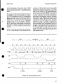
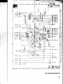
..-:-EXCHANGE-.... C f - - - - - - - - - - i S B C 80/10B CONTROL BUS
+'O:
1
I
•
I
1 I
' " ' C f - - - - - - - - - - - IOBS - -
BUSYI
ADDRESSI
DATA
COMMANDI
I
~
_.1. ___ :..
1
\
-----,.....
_.1. _____
-1
--r--
, ..
ADDRESS STABLE
-~---:1 , ..
DATA STABLE
IDS ~
I CMO
lAS
+
XACK
SAMPLING
POINT
tACK1~
XACKI
BUS
STATUS
SAMPLING
POINTS
•
+
I-
.. II
I ACK2
I
t
+
+
•
-
-IAH.IOHW
•-
I
t
IXKO
PSI26
Figure 2-3. Bus Exchange Timing (Write)
2-12
•
OTHER
1 I
1 I
I
BPRN
1
•
1 I
1
I
I
-
- - - - - - - - - . ..;1 iMASTER
I
I
1
I
•
•
Preparation for Use
iSBC80/10B
•
Table 2-13. iSBC 80/l0B DC Characteristics
Signals
ADRO/-ADRF
ADDRESS
•
VOL
VOH
VIL
VIH
IlL
IIH
*CL
.
MRDC/, MWTCI
IORC/, IOWCI
•
VOH
Output High Voltage
VOL
VOH
VIL
iLH
ILL
*CL
VIL
VIH
ilL
ilH
'CL
BPRN/, XACKI
•
•
OPEN COLLECTOR
INT
(SYSTEM RESET)
BCLK/, CCLKI
•
VIL
VIH
ilL
IIH
'CL
BUSYI
Input Low Voltage
Input High Voltage
Input Current at Low V
Input Current at High V
Capacitive Load
Output Low Voltage
VIH
IlL
INT11
Output Low Voltage
Output High Voltage
VOL
ILH
ILL
*CL
DATO/-DA T7 I
Parameter
Description
Symbol
VOL
'CL
Test
Conditions
IOL = 24 mA
IOH= 15 mA
IOL = 32 mA
IOH = -5.2 mA
Vo = 2.4
Vo = 0.4
Output Low Voltage
Output High Voltage
Input Low Voltage
Input High Voltage
Input Current at Low V
Output Leakage High
Output Leakage Low
IOL = 32 mA
IOH = -5 mA
V
V
40
-40
IlA
IlA
pF
V
V
V
V
mA
0.5
2.4
0.9
VIN = 0.45
Vo = 5.25
Vo = 0.45
-0.2
50
200
Il A
IlA
pF
18
Input Current at High V
VIN = 5.5
V
0.8
2.0
Capacitive Load
-2.2
V
mA
1
mA
18
pF
0.8
V
2.0
VIN =.5
VIN = 2.7
IOL = 48 mA
Capacitive Load
IOL = 48 mA
VOH
VIL
VIH
Open Collector
ilH
Output High Voltage
Input Low Voltage
Input High Voltage
Input Current at High V
ilL
'CL
Input Current at Low V
Capacitive Load
VIN = 0.3
V
-2.1
Capacitive Load
Capacitive Load
0.4
2.0
VIN = 0.4V
Output Low Voltage
Output High Voltage
Il A
pF
15
Input Low Voltage
Input High Voltage
Input Current at Low V
Output Low Voltage
18
2.4
Capacitive Load
Low Voltage
High Voltage
Current at Low V
Current at High V
V
V
V
V
mA
-0.2
20
VIN = 0.45
VIN = 5.5
Output Low Voltage
'CL
0.4
2.4
0.8
Output Leakage High
Output Leakage Low
Capacitive Load
Input
Input
Input
Input
Units
Max.
2.0
VOL
VOL
VOH
Min.
.3
Il A
mA
18
pF
0.4
V
18
pF
0.4
V
0.8
2.0
VIN = 5.5
0.2
-0.9
18
: IOL = 32 mA
IOH = -5.2 mA
0.5
2.4
18
V
V
mA
mA
pF
V
V
pF
'Capacitive values are approximations only.
2-13
iSBC80/10B
Preparation for Use
Table 2-13. iSBC SO/1OB DC Characteristics (Cont'd)
Parameter
Description
Symbol
Signals
I,L
I'H
'CL
PORT E4
BIDIRECTIONAL
DRIVERS
Min.
Max.
Input Low Voltage
V,L
V,H
EXT INTROI
Test
Conditions
Input High Voltage
Input Current at Low V
Input Current at High V
0.8
V
V
V,N = 0.4V
-6.8
V,N = 5.5V
2
18
mA
mA
2.0
Capacitive Load
VOL
VOH
V,L
Output Low Voltage
Output High Voltage
V,H
I,L
Input High Voltage
IOL = 27 mA
IOH= -7 mA
V
V
.9
V
2.0
Input Current at Low V
V,N = 0.45
Output Leakage High
Vo = 5.25
Capacitive Load
8255A
VOL
Output Low Voltage
IOL = 1.7 mA
DRIVERI
VOH
Output High Voltage
IOH =
RECEIVER
V,L
V,H
Input Low Voltage
I,L
Input Current at Low V
I'H
'CL
Input Current at High V
-5.2
V
mA
.3
mA
18
pF
.45
-50~A
pF
.5
2.4
Input Low Voltage
ILH
'CL
Units
2.4
V
V
.8
V
V
V,N = 0.45
10
~A
V,N = 5.0
10
~A
18
pF
Input High Voltage
2.0
Capacitive Load
•
'Capacitive values are approximations only.
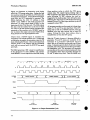
ADDRESSI
-
DATA STABLE
DATA
-
! - IOHW
~
lAS
•
•
i-ICSEP
I
I
IACK1 -
XACKI
I---'AH
I-Ios-I
COMMANDI
XACK
SAMPLING
POINT
-
ADDRESS STABLE
•
it
•
ICY
t ACK2
I
-
i-IXKO
I
I
I
I
EXTERNAL DEVICE
COMPLETED WRITE
PSI28
Figure 2-4. Memory and I/O Read Timing
2-14
Preparation for Use
iSBC80/10B
Table 2-14. AC Characteristics with Continuous Bus Control
•
Overall
Multlbus
Standard
Parameter
..
•
•
•
•
iSBC SO/1OA
Former
Parameter
Continuous Bus Control
Read
Memory Write
Description
Min.
(ns)
Max. Min.
(ns) (ns)
Max.
(ns)
Min.
(ns)
tAS
tAS
82
82
658
Address Setup Time
to Command
tAH
tAH
79
0
79
Address Hold Time
tos
tos
113
-
113
Data Setup Time
to Command
tOHR,
tOHw
tOH
79
79
Data Hold Time
IxACK
tACKO
63
191
tACK1
546
684
tACK2
1029 1177
0
Remarks
Max.
(ns)
1st ACK Sampling Point
of Current Cycle
Generates 0 Wait States
-84
137
2nd ACK Sampling Point
of Current Cycle
Generates 1 Wait State
399
630
3rd ACK Sampling Point
of Current Cycle
Generates 2 Wait States
493
Icy
tCY
483
tCSEP
tSEP
259
tCMO
twc
IACC
tACC
344
tXKD
0
tXKO
0
100
tecy
tecy
107
110
Bus Clock Cycle Time
80/10 Generator
tew
tew
25
85
Bus Clock Low or
High Periods
80/10 Generator
tiNT
tiNT
3000
Initialization Width
After all voltages have
stabilized
ACK & SPRN Sample
Cycle Time
613
596
259
840
1412
Note 2 Command Separation
1516
344
0
0
Command Width
Read, 0 Wait States
Write, 2 Wait States
Read Access Time
See Note 1
XACK Delay from
Valid Data or Write
100
0
100
XACK Turn Off Delay
NOTES:
1. Max assumes no acknowledge delays.
2. Write Command to next Read Command separation .
•
2-<15
Preparation for Use
iSBC80/10B
Table 2-15. AC Characteristics with Bus Exchange
Overall
Multlbu8
Standard
Parameter
ISBC 80/10A
Former
Parameter
Continuous Bus Control
Read
MemoryWrHe
Description
Min. Max. Min. Max.
(ns) (ns) (ns) (ns)
Min.
(ns)
Remarks
Max.
(ns)
tAS
tAS
82
82
658
Address Setup Time
to Command
tAH
tAH
61
0
61
Address Hold Time
tos
tos
113
-
113
Data Setup Time to
Command
tOHR,
tOHW
tOH
61
0
61
Data Hold Time
tACK
1ACKO
63
191
tACK1
546
684
tACK2
1029 1174
•
•
I
tCY
tCY
tcMO
twc
tACC
tACC
483
tXKO
0
tOBS
tOBY
tOBY
2nd ACK Sampling Point
of Current Cycle
Generates 1 Wait State
399
630
Third ACK Sampling Point
of Current Cycle
Generates 2 Wait States
544
•
ACK & BPRN Sample
Cycle Time
840
!
1412
1516
0
100
Generates 0 Wait States
132
344
0
1st ACK Sampling Point
of Current Cycle
-84
493
596
tXKO
•
0
Command Width
Read, 0 Wait States
Write, 2 Wait States
Read Access Time
See Note 1
XACK Delay from
Valid Data or Write
100
0
100
XACK Turn Off Delay
3500
Bus Sample to
Exchange Initiation
1217
Bus Busy Turn On
Delay
Note:
1, Memory and 1/0 access occurs without wait states.
•
See Note 1
•
•
•
2-16
Preparation for Use
iSBC80/l0B
•
ADDRESSI
~
.
ADDRESS STABLE
~
--I
I...-IDHR
DATA STABLE-~I
_
DATA
I ACC
~
COMMANDI
.
•
XACKI
SAMPLING
POINT
-
~
i - - IAS
tCMO
XACKI
~IXACK
0(
IAH
-
I
/-IXKD
ICY
-
1...-lxKo
II
---
PSl27
Figure 2-5. Memory and I/O Write Timing
•
•
..
•
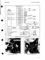
2-23. PRIORITY RESOLUTION
If the iSBC 80/10B board is the only master in your
system, it may be placed into any slot in the iSBC
604/614 Cardcage and Backplane which does not
have pin 15 (BPRN/) grounded.
The iSBC 80/lOB board bus structure allows you to
interface one other Multibus compatible master to
your system. In this configuration, theiSBC 80/10B
board will always have the lower priority of the two
masters. There are two methods of implementing the
dual master configuration in the iSBC 604/614
Cardcage and Backplane. The first method is
recommended for full Multibus line compatibility.
The second method should be used only when the
iSBC 80110B board is being used as a direct
replacementfor the iSBC 80/1 OA board in an existing
system.
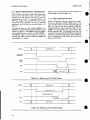
The first method is illustrated in figure 2-6. In this
configuration the other master is placed into any
cardcage slot which has pin 15 (BPRN/) of the
backplane grounded. Jumper pair 84 to 85 on the
iSBC 80110B board must then be removed and
replaced with a jumper between 85 and 86. The iSBC
SO/lOB board would then be placed in an adjacent
slot to the other master for proper operation. To
illustrate, the first method is implemented in the
following example:
a. Place other master in cardcage slot J2 .
b. Ground J2 pin 15 (BPRN I) by installing ajumper
wire between wire wrap posts Band N (figure
2-6).
c. Remove jumper 84 to 85 on the iSBC 80/10B
board. Install a jumper between 85 and 86.
d. Place the iSBC 80110B board in slot J3.
The second method of implementing the dual master
priority configuration is shown in figure 2-7. In this
configuration the other master is also placed into any
cardcage slot which has pin 15 (BPRN /) grounded. A
jumper must then be installed between pin 18 of the
other master and. pin 15 of the iSBC 80/10B board. A
slot must also be skipped in this scheme. To
illustrate, the_second method is implemented in the
following example:
a. Place other master in cardcage slot J2.
b. Add a jumper wire between wire wrap posts A
and E on the backplane (figure 2-7).
c. Install the iSBC 80/10B board into slot J4.
d. Alternatively, the iSBC 80/lOB board could be
placed in slot J5. In this case, the jumper wire
would be installed between wire wrap posts A
and H on the backplane.
2·17
iSBC80/10B
Preparation for Use
B
BPRNI
15
BPROI
16
BPRO/
18
N
E L
C M
15
15
16
-=
16
-=
18
18
~
J2
J3
J4
(OTHER
MASTER)
(iSBC 80/10B)
(OPEN)
•
16
o
18
F
0
A
P1
H K
G
'7
I
J5
ft
(OPEN)
,
•
I
Figure 2-6. Multibus™ Compatible Priority Resolution
BPRNI
15
15
BPROI
16
16
BPROI
18
G
P1
J2
J3
J4
J5
(OTHER
MASTER)
(OPEN)
(iSBC 80/10B)
(OPEN)
•
Figure 2-7. Replacement Method Priority Resolution
2-24. MUL TIMODULE CONFIGURATION
recommend a specific method. A typical memory
protect scheme could be implemented as follows:
The iSBC 80/lOB board is Multimodule compatible.
Multimodule boards are special purpose, add-on
circuit boards which reside directly on the component
side of the iSBC 80/10B board and are interfaced
through connector J 4. For specific Multimodule
installation instructions, refer to the corresponding
Multimodule hardware reference manual.
2-25. POWER FAIL AND MEMORY
PROTECT CONFIGURATION
A power-fail and memory protect scheme may be
implemented to preserve RAM conten~ in the event
of an AC line failure. There are many ways to
implement such a scheme, however Intel does not
2-18
NOTE
Detailed timing information for a typical
power fail routine is provided in the Intel
Multibus Specification, Order Number
9800683.
a.
b.
Connect +5 volt battery supply leads to P2-4 and
P2-3 connectors. Connect returns to P2-1 and
P2-2.
Remove or cut W4 connection shown on figure
5-3, sheet 1, zone D6.
I
•
Preparation for Use
iSBC80/10B
•
c.
d.
e.
.
•
Remove jumper 87 to 88 and install jumper 88 to
89. Refer to figure 5-3, sheet 2, zone D7. This
connection enables PFINI to interrupt the CPU.
Connect MPROI to P2-20. Refer to figure 5-3,
sheet 4, zone D7. MPROI must be generated by
an external, battery operated latch, which is
triggered by ACLO and PFIN/.
Connect PFSN I to P2-17 and PFSRI to P2-13.
Refer to figure 5-3, sheet 7. The PFSNI input
and the PFSRI output should be connected to
Port C on PPI circuit U16, using jumper posts 12
and 14, respectively. This enables the PPI to
provide status to the CPU, to identify the powerfail interrupt as such, and subsequently reset the
PFSRI signal upon restart.
NOTE
Ensure that the upper and lower portions of
port C of the PPI circuit are configured to the
appropriate mode to allow operation with
PFSNI and PFSR/. Refer to Chapter il for
PPI programming information_
2-26. USING RMX-80 SOFTWARE
If your iSBC 80/10B board is used with Intel RMX -80
•
software, some hardware modifications may be
required for proper operation. Depending on the
nature of your application and the types of extensions
used, the iSBC 80110B board may require reconfiguration of the following:
a.
Baud rate selection jumpers.
b.
Clock source jumper.
c.
Interrupt jumper.
d.
PCI control line jumpers.
e.
Interface jumpers.
In addition, user software may require modification
to initialize and format the Programmable Peripheral Interface devices and the Programmable
Communication Interface device.
Refer to the RMXIBO User's Guide, Manual Order
Number 9800522, for complete instructions.
2-27. SERIAL 1/0 CABLING
Pin assignments and signal definitions for RS232C
serial I/O interface are listed in table 2-16. An Intel
iSBC 955 Cable Set is recommended for RS232C
interfacing_ One cable assembly consists of a
25-conductor flat cable with a 26-pin PC connector at
one end and an RS232C interface connector at the
other end. The second cable assembly includes an
RS232C connector at one end and has spade lugs at
the other end; the spade lugs are used to interface to a
teletypewriter. (See Appendix B for ASR-33 TTY
interface instructions.)
Table 2-16. Pin Assignments for Connector J3 (Serial I/O Interface)
Signal Name
Pin
1
•
3
5
7
2
-
4
-
RECEIVED DATA
6
REO TO SEND
9
11
CLEAR TO SEND
DATA SET READY
13
15
GND
DATA CARRIER RETURN
14
16
19
21
23
25
Signal Name
CHASSIS GND
TRANSMITTED DATA
8
10
12
17
•
Pin
-12 Volts
TTY Rx DATA
TTY Tx DATA
18
20
22
24
26
TTY RD CONTROL
Tx ClK/DATA TERMINAL ROY
TTY RD CONTROL RETURN
-
-
-
-
RECEIVE ClKITTY Rx DATA
RETUFlN/+12
TTY Tx DATA RETURN
GND
Note:
Even numbered pins are on the component side of the board. Pin number 1 is on extreme right of solder side (as viewed from
component side).
2-19
iSBC80/lOB
Preparation for Use
+12 and -12 Volt Outputs
A +12 volt level may be applied to J3-22 if this pin is
unused in your configuration (refer to figure 5-3,
sheet 6), by installing jumper W3. Likewise, a -12
volt level will be applied to J3-19 if jumper WI is
installed.
Table 2-17. J3/RS232C Connector
Pin Correspondence
Signal Name
CHASSIS GND
TRANSMITTED DATA
Ensure connector J3 is properly installed
and the pins are connected to appropriate
loads. Damage may result from improper
connection.
For OEM applications where cables will be made for
the iSBC BO/I0B board, it is important to note that
the mating connector for J3 has 26 pins whereas the
RS232C connector has 25 pins. Consequently, when
connecting the 26-pin mating connector to 25-conductor flat cable, be sure that the cable makes contact
with pins 1 and 2 of the mating connector and not
with pin 26. Table 2-17 provides pin correspondence
between connector J3 and the RS232C connector.
When attaching the cable to J3, be sure that the PC
connector is oriented properly with respect to pin 1 on
the edge connector. (Refer to the footnote in table
2-16.)
2-28. PARALLEL 1/0 CABLING
Parallel 110 ports E4, E5, E6, E8, E9, and EA are
controlled by two Intel 8255A Programmable
Peripheral Interface (PPI) devices and interfaced via
edge connector Jl and J2. Pin assignments for Jl
and J2 are listed in table 2-6; dccharacteristics ofthe
parallel 110 signals are given in table 2-13. Table
2-10 lists some 50-pin edge connectors that can be
used for interface to J1 and J2; flat crimp, solder, and
wirewrap connector types are listed.
An Intel iSBC 956 Cable Set, consisting of two cable
assemblies, is recommended for parallel 1/0 interfacing.
Both cable assemblies consist of a 50-conductor flat
cable with a 50-pin PC connector at one end. When
attaching the cable to Jl or J2, be sure that the
connector is oriented properly with respect to pin 1 on
the edge connector. (Refer to the footnote in table
2-16.)
The transmission path from the 110 source to the
iSBC 80/10B board should be limited to 3 meters (10
feet) maximum.
The following bulk cable types (or equivalent) are
recommended for interfacing with the parallel I/O
ports:
a. Cable, flat, 5O-conductor, 3M 3306-50.
2-20
RECEIVED DATA
TTY RD CONTROL
REO TO SEND
CLEAR TO SEND
DATA SET READY
GND
Tx ClK/DATA TERMINAL RDY
DATA CARRIER RETURN
TTY RD CONTROL RETURN
-12 VOLTS
J3
Connector
PIn No.
RS232C
Connector
Pin No.
1
2*
3
4*
5
6
7
8
9
10"
11
12*
13
14
15
16
17*
18*
19
1
14
2
15
3
16
4
17
5
18
6
19
7
20"
23
11
21*
RECEIVE ClK/TTY Rx
DATA RETURN/+12V
TTY Rx DATA
TTY Tx DATA RETURN
TTY Tx DATA
22
23
24
25
26*
20
8
21
9
22
•
I
•
•
-
24
12
25
13
-
Note:
* =Not Used on iSBC 80/10B board.
•
b. Cable, flat, 50-conductor (with ground plane),
3M 3380-50.
c. Cable, woven, 25-pair, 3M 3321-25.
5 Volt Output
In the standard factory configuration, pin J2-1 is
grounded (refer to figure 5-3, sheet 8). As an optional
connection, you may apply +5 volts to this pin by
removing jumper pair 26-27 and installing 27-28.
Ensure connector J2 is properly installed
and pin 1 is connected to an appropriate
load. Damage may result from improper
connection.
r
•
I
Preparation for Use
iSBC80/10B
•
2-29. BOARD INSTALLATION
I~
Always turn off the computer system power
supply before installing or removing the
iSBC SO/lOB board and before installing or
removing interface cables. Failure to take
these precautions can result in damage to
the board.
In an iSBC Single Board Computer based system,
install the iSBC 80/l0B board in any slot that has
not been wired for a dedicated function. In an
Intellec System, install the board in any slot except
slot 1 or 2. Make sure that auxiliary connector P2 (if
used) mates correctly with the user-installed
connector. Attach the appropriate cable assemblies
to connectors Jl through J3.
•
•
•
•
2-2112-22
•
•
,.
!
!
•
I
•
CHAPTER 3
PROGRAMMING INFORMATION
3-1. INTRODUCTION
This chapter provides programming instructions for
the two Programmable Peripheral Interface devices
(UI6, UI7) and the Programmable Communications
Interface device (UI8). Memory addressing and
system initialization information is also provided.
3-2. MEMORY ADDRESSING
•
The iSBC 80/lOB board can accommodate up to 16K
bytes of ROM/EPROM on-board. Additionally, up to
4K bytes of RAM may be installed on-board. However, it is only in this maximum configuration that
memory will be continuous, from 0000 to 4FFF
(Hexadecimal). In this maximum configuration,
ROM space runs from 0000 to 3FFF, and RAM space
runs from 4000 to 4FFF. None ofthis memory may be
addressed by another board or processor.
If you are using the iSBC 80/10B board in another
•
configuration, less than the maximum, a gap in
continous memory appears between the end of ROM
space and the beginning of RAM space. This
information is summarized in table 3-1. Memory
addresses which fall into the gap zone may be
assigned off-board, and accessed by the iSBC 80/1 DB
board via the Multibus lines.
If non-existant memory is addressed, the on-board
•
•
failsafe timer will expire in approximately 10
milliseconds, sending an acknowledge signal to the
CPU so that it may resume processing. For more
information on the failsafe timer, refer to section
2-18.
Table 3-1. Memory Addressing
ROM Devices
Address Space
1K x 8
2K x 8
4K x 8
0000 - OFFF
0000-1FFF
0000 - 3FFF
RAM Devices
Address Space
1K
2K
3K
4K
XCOO - XFFF
X800 - XBFF
X400 - X7FF
XOOO - X3FF
NOTE:
X prefix will be 3with 1Kor 2K ROM devices{nstalled; and 4
with 4K ROM devices installed. Refer to Chapter 2.
When the CPU is addressing on-board memory
(ROM/PROM or RAM), an internal PROM or RAM
Acknowledge (ACK/) is automatically generated to
prevent imposing a CPU wait state. When the CPU
is addressing system memory via the Multibus lines,
the CPU must first gain control of the Multibus lines
and, after the Memory Read or Memory Write
Command is given, must wait for a Transfer
Acknowledge (XACK/) to be received from the
addressed memory device.
3-3. I/O ADDRESSING
The on-board 8080A microprocessor (CPU) communicates with the programmable devices through a
sequence ofI/O Read and 110 Write Commands. As
shown in table ~1-2, each of these devices recognizes
several separate hexadecimal I/O addresses that are
used to control the various programmable functions.
Where two hexadecimal addresses are listed for a
single function, either address may be used. For
example, an I/O Read Command to ED or EF will
read the status of the 825IA PCl.
NOTE
The on-board I/O functions are not accessible to another bus master via the Multibus
lines.
Table 3-2. I/O Addressing
1/0
Address
Device
Function
E4
E5
E6
E7
U16
PPI
Read/Write Port A (J1)
Read/Write Port B (J1)
Read/Write Port C (J1)
Write: Control Byte
E8
E9
EA
EB
U17
PPI
Read/Write Port A (J2)
Read/Write Port B (J2)
Read/Write Port C (J2)
Write: Control Byte
U18
PCI
Write:
Read:
Write:
Read:
EC or EE
ED or EF
Fo-F7
F8-FF
If Multimodule is
installed
Data (J3)
Data (J3)
Mode or Command
Status
Multimodule MCSOI (J4)
Multimodule MCS11 (J4)
3-1
Programming Information
3-4. SYSTEM INITIALIZATION
When power is initially applied to the system, an
Initialize (INITI) signal is automatically generated
that clears the internal Program Counter, Instruction Register, and Interrupt Enable flip-flop and
"resets" the 8251A PCI, and the 8255A PPI devices as
follows:
a. The 8251A PCI is set to an "idle" mode, waiting
for a set of Command Words to program the
desired function.
iSBC80/10B
(4) External sync detect (not supported by
iSBC SO/10B
(5) Single or double character sync
(4) Even/odd parity generation and check
(5) Number of stop bits
b. For Async Mode:
(1) Baud rate factor (Xl, X16, or X64)
(2) Character length
(3) Parity enable
•
Instruction word and data transmission formats for
synchronous and asynchronous modes are shown in
figures 3-1 through 3-4.
b. All three ports of each 8255A PPI are set to the
input mode.
,
i
•
I
The INITI signal is also gated onto the Multibus
lines to set the remainder of the system components
to a known internal state.
The INIT I signal can also be generated by an
auxiliary RESET switch. Pressing and releasing the
RESET switch produces the same effect as the INITI
signal described above.
.....-'-...,-':.,-.:.,-D....;...
0)
01
0,
00
EPPEN~
~
CHARACTER LENGTH
0
1
0
1
0
0
1
1
5
6
BITS
BITS
1
BITS
BITS
8
L ______
l
PARITY ENABLE
f1 : ENABLE)
fO'" DI$ABLEt
' - - - - - - - - - - - - 1 EVEN PARITY GENERATlONfCHECK
1 • EVEN
0=000
3-5. 8251A PCI (USART) PROGRAMMING
' - - - - - - - - - - EXTERNAL SYNC DETECT
1 • SYNDET IS AN INPUT
The PCI converts parallel output data into virtually
any serial output data format (including IBM BiSync) for half- or full-duplex operation. The PCI also
converts serial input data into parallel data format.
Prior to starting transmitting or receiving data, the
PCI must be loaded with a set of control words. These
control words, which define the complete functional
operation of the PCI, must immediately follow a reset
(internal or external). The control words are either a
Mode instruction or a Command instruction.
o • SY"'DET IS AN OUTPUT
- - - - - - - - - - SINGLE CHARACTER SYNC
1 : SINGLE SYNC CHARACTER
o : DOUBLE SYNC CHARACTER
I
•
Figure 3-1. PCI Synchronous Mode
Instruction Word Format
CPU BYTES {S·B BfTS/CHARI
;'
DATA CHARACTERS
L -_ _.....
I - ,_ _- - '
ASSEMBLED SERIAL DATA OUTPUT (TxD)
OAT A
CHA~,....:AC_TE_RS_---,
3-6. MODE INSTRUCTION FORMAT
I
~
RECEIVE FORMAT
The Mode instruction word defines the general
characteristics of the PCI and must follow a reset
operation. Once the Mode instruction word has been
written into the PCI, sync characters or command
instructions may be inserted. The Mode instruction
word defines the following:
a. For Sync Mode:
(1) Character length
(2) Parity enable
(3) Even/odd parity generation and check
3-2
!
SERIAL OAT A INPUT IR.QI
SYNC
CHAR 1
SYNC
CHAR ~
I
DATA
CHA~~
,....C_TE_RS_----'
CPU BYTES (S-8 BITS/CHAR)
.------illl------,
OAT A CHARACTERS
L -_ _...., ....
, _ _- '
Figure 3-2. PCI Synchronous Mode
Transmission Format
•
Programming Information
iSBC80/10B
•
3-B. COMMAND INSTRUCTION FORMAT
The Command instruction word shown in figure 3-5
controls the operation of the addressed PCl. A
Command instruction must follow the mode and/or
sync words and, once the Command instruction is
written, data can be transmitted or received by the
PCl.
CHARACHR LENGTH
0
1
0
0
0
1
1
5
BITS
BITS
•
7
8ITS
8
BITS
PARITY ENABLE
1 ENABLE
0
1
DISABLE
[VEN PARITY GENERATION/CHE C<
1" EVEN
0 ODD
NUMBE R OF STOP BITS
TRANSMIT ENABLE
1"
•
INVALID
1
lYJ
2
BIT
BITS
BITS
en~ble
o " disable
(ONLY EFFECTS Tx; RII. NEVER
DATA TERMINAL
REOUIRES MORE THAN ONE
STQPBln
READY
"high" Will force OT R
output 10 letO
Figure 3-3. PCI Asynchronous Mode
Instruction Word Format
RECEIVE ENABLE
1
0
o
enable
disable
SEND BREAK
000,----
o.
GENERATED
BV82S1A
STt!
Brrs L
----I
L -_ _ _ _ _ _
•
DOES NOT APPEAR
000,----0.0NTHEDATA8US
RECEIVER INPUT
tt
------,
R.Q
START
~
t
t
S
1L.._._IT_....
~
__
OA_T-iA .I-IT_...I_.......;;~..J
"low"
----I ~~~:~~T~:D
o ~ normal operatton
L -_ _ _ _
ERROR RESET
1" reset error flags
PE. DE, FE
ST~
arTS
L
L -_ _ _ _ _ _ _ _ _ _
I
REQUEST TO SENO
"high" will torce RTS
output to lero
PROGRAMMED
CHARACTER
LENGTH
----------1
TRANSMISSION FORMAT
DATA
INTERNAL RESET
"high" returns 8251A to
Mode Instruction Format
CPU BYTE 15-8 BITS/CHARI
C~+ACTER
-----------1
ASSEMBLED SERIAL DATA OUTPUT fT.DI
ENTER HUNT MODE-
1" enable search for Sync
Ch.racte"
O_A_TA_C~H~AR-A-CT-.-R-..JL.........;;~...I-~~~I=J
' - -__- ' -__
•
RECEIVE FORMAT
SERIAL DATA INPUT IR.OI
DATA CHARACTER
STOD
Figure 3-5. PCI Command
Instruction Word Format
BITS
~-----'------'---'"
CPU BYTE (58 81TS/CHAR'-
OA TA
CH~RACTE R
'-------4,;1------'
·NOTE IF CHARACTER LENGTH IS DEFINED AS S. 60R 1
BITS THE UNUSED BITS ARE SE T TO ··lERO··
Figure 3-4. PCI Asynchronous Mode
Transmission Format
It is not necessary for a Command instruction to
precede all data transactions; only those transactions that require a change in the Command
instruction. An example is a change in the enable
transmit bit or enable receive hit. Command
instructions can be written to the PCI at any time
after one or more data operations.
3-7. SYNC CHARACTERS
•
Sync characters are written to the PCI in the
synchronous mode only. The PCI can be programmed for either one or two sync characters; the format
of the sync characters is at the option of the
programmer.
After initialization, always read the chip status and
check for the TxRDY bit prior to writing either data or
command words to the PCI. This ensures that any
prior input is not overwritten and lost. Note that
issuing a Command instruction with bit 6 (IR) set will
return the PCI to the Mode instruction format.
3-3
Programming Information
iSBC80/l0B
3-9. RESET
To change the Mode instruction word, the PCI must
receive a Reset command. The next word written to
the PCI after a Reset command is assumed to be a
Mode instruction. Similarly, for sync mode, the next
word after a Mode instruction is assumed to be one or
more sync characters. All control words written into
the PCI after the Mode instruction (and/or the sync
character) are assumed to be Command instructions.
3-10. ADDRESSING
The PCI device uses two consecutive pairs of
addresses. The lower of the two addresses in each
pair is used to read and write 110 data; the upper
address in each pair is used to write mode and
command words and to read the pcr status. (Refer to
table 3-2.)
3-11. INITIALIZATION
A typical PCI initialization and 110 data sequence is
presented in figure 3-6. The PCI device is initialized
in four steps:
a. Reset pcr to Mode instruction format.
b. Write Mode instruction word. One function of
mode word is to specify synchronous or asynchronous operation.
c. If synchronous mode is selected, write one or two
sync characters as required.
d. Write Command instruction word.
To avoid spurious interrupts during PCI initialization, disable the PCI interrupt. This can be done by
disabling the CPU interrupts by executing a DI
instruction.
First, reset the PCI device by writing a Command
instruction to location ED (or EF). The Command
instruction must have bit 6 set (IR6=I); all other bits
are immateriaL
NOTE
This reset procedure should be used only if
the pcr has been completely initialized, or if
the initialization procedure has reached the
point that the PCI is ready to receive a
Command word. For example, if the reset
command is written when the initialization
sequence calls for a sync character, then
subsequent programming will be in error.
N ext, write a Mode instruction word to the PCI. (See
figures 3-1 through 3-4.) A typical subroutine for
writing both Mode and Command instructions is
given in table 3-3.
If the PCI is programmed for the synchronous mode,
write one or two sync characters depending on the
transmission format.
ADDRESS
RESET
ED
MODE INSTRUCTION
ED
SYNC CHARACTER 1
ED
SYNC CHARACTER 2
ED
COMMAND INSTRUCTION
;;
COMMAND INSTRUCTION
EC
DATA 1/0
ED
COMMAND INSTRUCTION
3-12. OPERATION
Normal operating procedures use data 110 read and
write, status read, and Command instruction write
operations. Programming and addressing procedures for the above are summarized in the following
paragraphs.
~
'The second sync character is skipped if Mode instruction
has programmed PCI to single character internal sync
mode. Both sync characters are skipped if Mode instruction
has programmed PCI to async mode.
Figure 3-6. Typical PCI
Initialization and Data 1/0 Sequence
3-4
•
SYNC MODE
ONLY'
DATA 110
ED
•
Finally, write a Command instruction word to the
PCI. Refer to figure 3-5 and table 3-3_
}
EC
•
NOTE
After the PCI has been initialized, always
check the status of the TxRDY bit prior to
writing data or writing a new command
word to the PCI. The TxRDY bit must be true
to prevent overwriting and subsequent loss
of command or data words. The TxRDY bit
is inactive until initialization has been
completed; therefore, do not check TxRDY
until after the command word, which
concludes the initialization procedure, has
been written.
•
I
'.
I
Programming Information
iSBC80/10B
•
Table 3-3. Typical PCI Mode or Command Instruction Subroutine
;CMD2 OUTPUTS CG,~TROL WORD OR MODE WORD TO PCI.
;USES-STAT; DESTROYS-NOTHING.
CMD2:
LP:
EXTRN
STAT
PUSH
CALL
ANI
JZ
POP
OUT
RET
PSW
STAT
1
LP
PSW
OEDH
;SAVE DATA AND CPU STATUS
;GET PCI STATUS
;CHECK TXRDY
;TXRDY MUST BE TRUE
;RESTORE DATA AND CPU STATUS;
;SEND COMMAND/MODE WORD TO PCI
END
•
•
Prior to any operating change, a new command word
must be written with command bits changed as
appropriate. (Refer to figure 3-5 and table 3-3.)
character for transmission. TxRDY is automatically
reset when the CPU loads a character into the PCL
For data receive or transmit operations perform a
read or write, respectively, to the PCL Tables 3-4 and
3-5 provide examples of typical character read and
write subroutines.
Similarly, during normal receive operation, the PCI
generates a Reeeive Ready (RxRDY) signal that
indicates that a character has been received and is
ready for input to the CPU. RxRDY is automatically
reset when a character is read by the CPU.
During normal transmit operation, the PCI
generates a Transmit Ready (TxRDY) signal that
indicates that the PCI is ready to accept a data
The TxRDY and RxRDY outputs of the PCI can be
used to interrupt the CPU. Refer to section 2-14 for
instructions .
Table 3-4. Typical PCI Data Character Read Subroutine
;RX1 READS DATA CHARACTER FROM PCI.
;USES-STAT; DESTROYS-A, FLAGS.
RX1:
•
EXTRN
STAT
CALL
ANI
JZ
IN
RET
STAT
2
RX1
OECH
;GET PCI STATUS
;CHECK FOR RXRDY
;RXRDY MUST BE TRUE
;READ DATA FROM PCI
END
Table 3-5. Typical PCI Data Character Write Subroutine
;TX1 WRITES DATA CHARACTER FROM REG A TO PCI
;USES-STAT; DESTROYS NOTHING.
TX1:
TX11:
•
EXTRN
STAT
PUSH
CALL
ANI
JZ
POP
OUT
RET
PSW
STAT
1
TX11
PSW
OECH
;SAVE DATA AND CPU STATUS
;GET PCI STATUS
;CHECK FOR TXRDY
;TXADY MUST BE TRUE
;RESTORE DATA AND CPU STATUS
;SEND DATA TO PCI
END
3-5
iSBCSO/lOB
Programming Information
,
to control the 24 lines (3 ports) on each of the two
connectors. Line identification is provided in table
2-6.
The CPU can determine the status of the serial 1/0
port by issuing an I/O Read Command to the upper
address (ED or EF) of the PCI device. The format of
the status word is shown in figure 3-7. A typical
status read subroutine is given in table 3-6.
Each of the six ports (three on each 8255A device)
may be independently programmed for a different
I/O configuration. All the possible configurations
are summarized in table 3-7.
3-13. 8255A PPI PROGRAMMING
The iSBC 80/10B board has a total of 48 parallel I/O
lines. Half of these use connector Jl and the other
half use connector J2. One 8255A PPI device is used
DSR
I
SYNDET
I
FE
I
DE
I
PE
I
TXE
•
Notice that port operation is not identified for each
PPI device, although all six device ports may be
DO
01
I
•
I
RXRDY
I
I
•
I
'--
TXRDY
OVERRUN ERROR
11Ie OE Ilag is sel when Ihe CPU dOH
naI raid a characler befall! Ihe nell
one becomes available. II is resel by
file ER bit ollhe Command inslruction.
OE does nol inhibil operalion ollhe
8251; however. Ihe praviGusly overrun
character is 10Sl.
FRAMING ERROR (ASYNC ONLY)
FEII.g is set whennalid slop bil is not
detected al end 01 every characler. II is
is resel by ER bit 01 Command inslrue·
tion. FE dB nol inhibit operltion 01
8251A.
L-
TIWISMITTER READY
IndiClles USART is ready ID Iccepll
data character or commlnd.
'---
RECEIVER READY
IlIdiClles USART has received a chlr·
acter an its serial input Ind is ready
10 lranster illo file CPU.
TRANSMITTER EMPTY
Indiclles Ihil plrallel to serill _.
verter in lransmitter il Imply.
PARITY ERROR
PE IIlg Is .11 when a Plrity ern" il
detected. II is relll by ER bit 01 Com·
mind inslruction. PE does nol inhibit
operation of 8251 A.
SYNC DETECT
Whln lei for intimal sync delect indio
ellis IhII chmcter sync has been
achieved Ind 8251A is reldy for dall.
DATA SET READY
DSR is general purpose. Nonnally
used to lest modem conditions such as
DIIa Sel Ready.
Figure 3-7. PCI Status Read Format
.
Table 3-6. Typical PCI Status Read Subroutine
;STAT READS PCI STATUS
;USES-NOTHING; DESTROYS-A.
;STAT
IN
RET
END
3-6
OEDH
;GET PCI STATUS
•
Programming Information
iSBC80/10B
•
mode. Refer to section 2-17 for instructions on this
conversion .
Table 3-7. Parallel 110
Interface Configurations
A description of 8255A operation is provided in
Chapter 4.
Port E4 (Group 1 Port A J1)
Mode
Mode
Mode
Mode
Mode
0
0
1
1
2
Input
Output (Latched)
Input (Strobed)
Output (Latched)
Bidirectional
3-14. CONTROL WORD FORMAT
The control word format shown in figure 3-8 is used to
initialize each PPI port. Note that the three ports on
each PPI device are separated into two groups.
Group A (control word bits 3 through 6) defines the
operating mode for Port A and the upper four bits of
Port C. Group B (control word bits 0 through 2)
defines the operating mode for Port B and the lower
four bits of Port C. Bit 7 of the control word controls
the mode set flag. Control words are sent to Port E7
for the JI PPI device, or the Port EB for the J2 PPI
device (table 3-2). There are restrictions associated
with the use of c:ertain ports. Refer to table 3-7 and
sections 3-17 through 3-22.
Port ES (Group 1 Port B J1)
•
•
Mode
Mode
Mode
Mode
0
0
1
1
Input
Output (Latched)
Input (Strobed)
Output (Latched)
Port E6 (Group 1 Port C J1)
Mode 0
Mode 0
8 Bit Input
8 Bit Output (Latched)
Note:
Control mode dependent upon
Port A and B mode.
Ports Ea and E9 (Group 2 Port A,B J2)
Mode 0
Mode 0
3-15. ADDRESSING
Input
Output (Latched)
The JI PPI (UI6) uses three consecutive data
addresses: E4 through E6, plus command port
E7. The J2 PPI (UI7) also uses three consecutive
data addresses: E8 through EA, plus command port
EB. Refer to table 3-2.
Port EA (Group 2 Port C J2)
•
Mode 0
Mode 0
Mode 0
Mode 0
8 Bit Input
8 Bit Output
4 Bit Input/4 Bit Output
(Unlatched/Latched)
4 Bit Outputl4 Bit Input
(Latched/Unlatched)
3-16. INITIALIZATION
programmed as either inputs or outputs. Also, theJI
ports can fully utilize the PPI modes and external
interrupt capabilities (section 4-30). However, theJ2
ports may only operate in mode O.
•
A default jumper sets the JI, port E4 bidirectional
data buffers to the output mode. An optional jump
connection allows the data buffers for this port to be
set to the input mode or to allow bit 6 of Port E6 to set
the data buffers to either the input or the output
To initialize a PPI, write a control word to its control
port (E7 or EB). Refer to figure 3-8 and table 3-8 and
assume that the control word is 92 (hexadecimal).
This initializes the PPI as follows:
a.
b.
c.
d.
e.
Mode Set Flag active
Port A (E4 or E8) set to Mode 0 Input
Port C (EA or E6) upper set to Mode 0 Output
Port B (E9 or E5) set to Mode 0 Input
Port C (EA or E6) lower set to Mode 0 Output
Table 3-8. Typical PPI Initialization Subroutine
;INTPAR INITIALIZES PARALLEL PORTS.
;USES NOTHING; DESTROYS-A.
INTPAR:
•
MVI
OUT
RET
A,92H
OEBH
;MODE WORD (PPI PORT A&B IN, C OUT).
;SEND MODE WORD TO PPI
END
3-7
Programming Information
iSBCSOIlOB
Single Bit Set/Reset Feature
CONTROL WORD
I D71
D. D, 1D. I D,
Any of the eight bits of Port C can be Set or Reset
using a single output instruction (see figure 3-9).
This feature reduces software requirements in
Control-based applications.
I I I I
D,
D,
Do
LJ
GROUP 8
-
\
CONTROL WORD
•
PORT C (L.OWER~
1'" INPUT
0'" OUTPUT
PORT B
81T SET/RESET
1" INPUT
0" OUTPUT
l ' SET
0" RESET
MODE SELECTION
0= MODE 0
1 =MODE 1
I
PORT C (UPt>ERI
, .. INPUT
0= OUTPUT
BIT SET/RESET FLAG
O· ACTIVE
PORT A
,,, INPUT
OUTPUT
o~
MODE SElECTION
00:: MODE 0
01 " MODE 1
lX" MODE 2
r
"I
MODE SET FLAG
1· ACTIVE
Figure 3-S. PPI Control Word Format
3-17. OPERATION
The primary considerations in determining how to
operate each of the six I/O ports are:
a. choice of operating mode (as defined in table 3-7),
b. direction of data flow (input, output or bidirectional),
c. choice of driver/termination networks.
In the following paragraphs, we will define the
capabilities of each port and summarize, in tables,
information necessary to use the port in each of its
potential configurations. Each table will list the port
I/O address, the control register address and the
format for the control word which is sent to the PPI by
the CPU and which specifies the particular configuration to be used. Each table will also summarize the
relevant information concerning the choice and use
of driver/termination networks, the data polarity,
the connecting of jumpers and what they enable, and
any restrictions on the use of the other two ports in
each group.
•
,
GROUP A
3-8
•
•
Figure 3-9. PPI Port C Bit Set/RESET
Control Word Format
When Port C is being used as status/control for Port
A or B, these bits can be set or reset by using the Bit
Set/Reset operation just as if they were data output
ports.
Interrupt Control Functions
When the PPI is programmed to operate in Mode 1 or
Mode 2, control signals are provided that can be used
as interrupt request inputs to the CPU. The interrupt
request signals, generated from Port C, can be
inhibited or enabled by setting or resetting the
associated INTE flip-flop, using the Bit Set/Reset
function of Port C.
This function allows the Programmer to disallow or
allow specific I/O devices to interrupt the CPU
without effecting any other device in the interrupt
structure.
•
INTE flip-flop definition:
(BIT-SET) - INTE is SET - Interrupt enable
(BIT-RESET) - INTE is RESET - Interrupt
disable
All Mask flip-flops are automatically reset during
mode selection and device Reset.
3-1S. PORT E4. Port E4 is the only port that
already includes a socketed bidirectional driver/
•
Programming Information
iSBC80/10B
•
•
•
•
•
termination network (8287 Octal Bus Transciever).
Port E4 is also the only port which can be programmed to function in anyone of the three PPI operating
modes. Before Port E4 is programmed for input or
output in anyone of the three modes, certain jumper
connections must be made to allow the port to
function properly in the chosen mode. Other jumper
connections must be made to enable interrupts when
Port E4 is in mode 1 or mode 2. In all, there are five
potential configurations for Port E4. All of the
necessary information for implementing each
configuration has been summarized in the following
tables:
PORT E4 CONFIGURATIONS
4-bit inputl4-bit output configuration is never
possible for Port E6.
NOTE
If Ports E4 and E5 are not both in mode 0,
then a driver network must be installed in
the sockets in U2 and a termination network
must be installed in U3 so that the Port E6
control lines can function properly.
3-21. PORTS E8 AND E9. Ports E8 and E9 can
be programmed for input or output but only in mode
O. The two potential configurations for each port are
summarized in the following tables:
Table
Direction
Mode
1. Mode 0
2. Mode 0
3. Mode 1
4. Mode 1
5. Mode 2
Input
Output (Latched)
Input (Strobed)
Output (Latched)
Bidirectional
Table 3-9
Table 3-10
Table 3-11
Table 3-12
Table 3-13
3-19. PORT E5. Port E5 can be programmed for
input or output in either mode or mode 1. If Port E5
is to be used for input, in either mode, terminator
networks must be installed in sockets U4 and U5. If
Port E5 is to be used for output, in either mode, driver
networks must be installed in sockets U 4 and
U5. When Port E5 is programmed for mode 1,
interrupts can be enabled by connecting jumper pair
9-10. The four potential configurations for Port E5
are summarized in the following tables:
°
Configurations
Table
Port
Mode
Direction
1. Port E8
Mode 0
Input
Table 3-20
2. Port E8
1. PortE9
Mode 0
Mode 0
Output (Latched)
Input
Table 3-21
Table 3-22
2. Port E9
Mode 0
Output (Latched)
Table 3-23
3-22. PORT EA. All eight bits of Port EA can be
programmed for mode 0 input or output, or four bits
can be programmed for mode 0 input while the other
four bits are programmed for mode 0 output. The
four potential configurations for Port EA are
summarized in the following tables:
PORT EA CONFIGURATIONS
Port E5 Configurations
Table
Mode
1.
2.
3.
4.
Mode
Mode
Mode
Mode
Mode
Direction
0
0
1
1
Input
Output (Latched)
Input (Strobed)
Output (Latched)
Table
Table
Table
Table
3-14
3-15
3-16
3-17
3-20. PORT E6. The use of Port E6 is dependent on
the modes programmed for Ports E4 and E5 (refer to
tables 3-9 to 3-17). While certain Port E6 bits are
available if Port E4 is in mode 1 or if Port E5 is in
mode 0, the use of Port E6 as an 8-bit data path is
restricted to those configurations that have both Port
E4 and Port E5 programmed for mode O. In this case,
all eight bits of Port E6 can be programn\ed for mode
o input (see table 3-18) or output (see table 3-19). A
Direction
Table
1. Mode 0
2. Mode 0
3. Mode 0
8-bit Input
8-bit Output (Latched)
Upper 4-bit Input/
Lower 4-bit Output
Table 3-24
Table 3-25
4. Mode 0
Upper 4-bit Output/
Lower 4-bit Input
Table 3-26
Table 3-27
After the PPI has been initialized, operation is
accomplished by performing a read or write operation to the appropriate port. A typical read subroutine is shown in table 3-28. A typical write subroutine is shown in table 3-29.
3-9
iSBC80/l0B
Programming Information
Table 3-9. Port E4, Mode 0 Input Configuration
Port Address: E4, Control Register Address: E7
7
6
5
4
3
2
0
'-1-'1-0-'-0-'--'-x-'-x-'-x-rI'~
Control Word Format:
•
DrlverlTermlnatlon Networks: 8287 Transceiver installed in socket U 1.
•
Data Polarity: Negative-true.
Jumper Connections: Remove 59-60.
Port E5 Restrictions: None; Port E5 can be programmed for mode 0 or mode 1, input or output (see Section 3-19).
Port E6 Restrictions: None; Port E6 can be programmed for mode 0, 8-bit input or output, unless Port E5 is in mode 1 (see
Section 3-20).
Table 3-10. Port E4, Mode 0 Latched Output Configuration
Port Address: E4, Control Register Address: E7
Control Word Format:
7
6
5
4
3
2
0
•
•
r---r-o-''-o-'--o-'-x-''-x-'--x-I'-'~
DriverlTermlnatlon Networks: 8287 Transceiver installed in socket U1.
Data Polarity: Negative-true.
Jumper Connections: Factory Default: 59-60 installed.
Port E5 Restrictions: None; Port E5 can be programmed for mode 0 or mode 1, input or output (see Section 3-19).
Port E6 Restrictions: None; Port E6 can be programmed for mode 0, input or output, unless Port E5 is in mode 1 (see Section
3-20).
•
Table 3-11. Port E4, Mode 1 Strobed Input Configuration
Port Address: E4, Control Register Address: E7
Control Word Format:
7
6
o
5
4
3
2
1
0/1
x
x
10
I :~
DrlverlTermlnatlon Networks: 8287 Transceiver permanently installed in U1. A driver network must be installed in U2 and a
termination network must be installed at U3.
Data Polarity: Negative-true. The polarity of Port E6 control outputs is dependent on the type of driver installed in U2.
•
•
Jumper Connections: 60-61 to enable input 8287, connect 19-20 to enable interrupt request via INT55/. Remove 59-60; 20-25;
19-24.
Port E5 Restrictions: None; Port E5 can be programmed for mode 0 or mode 1, input or output (see Section 3-19).
Port E6 Restrictions: Port E6 bits perform the following dedicated functions:
OBits 0, 1 and 2 - dedicated to control of Port E5 if it is in mode 1 (see tables 4-9 to 4-12).
OBit 3 - INTR (interrupt request) output for Port E4.
OBit 4 - STBI (strobe) input for Port E4.
OBit 5 - IBF (input buffer full) output for port E4.
OBit 6 and 7 - Only one bit c,m be used. If input, use bit 6; do not use bit 7. Bit 30fC()ntrol Word=1.lfoutput, use bit 7, do not
use bit 6. Bit 3 of Control Word=O.
3-10
•
Programming Information
iSBC80/10B
•
Table 3-12. Port E4" Mode 1 Latched Output Configuration
Port Address: E4, Control Register Address: F.7
Xl
65432
0
7
r-~-o~--'-o-r-x-'-x-'-x-'-I
Control Word Format:
DriveriTermination Networks: 8287 Transceiver permanently installed in U1. A driver network must be installed in U2 and a
termination network must be installed at U3.
Data Polarity: Negative-true. The polarity of Port C control outputs is dependent on the type of driver installed in U3.
Jumper Connections: 59-60 (defau It) to enable output at 8287, connect 19-20 to enable interrupt request via INT55/. Remove
20-25; 19-24.
•
Port E5 Restrictions: None; Port E5 can be programmed for mode 0 or mode 1, input or output (see Section 3-19) .
Port E6 Restrictions: Port E6 bits perform the following dedicated functions:
'Bits 0, 1 and 2 - dedicated to the control of Port E5 if it is in mode 1 (see tables 3-16 and 3-17).
'Bit 3 -
I NTR (interrupt request) output for Port E4.
*Bit 4 Bit 5 -
can be used for Input if bit 3 of control word=1
cannot be used if PC4 is used; can be used for output if control word bit 3=0 (PC4 cannot be used then).
*Bit 6
ACKI (acknowledge) input for Port E4.
*Bit 7 - OBFI (output buffer full) output for Port E4 .
•
Table 3-13. Port E4, Mode 2 Bidirectional Configuration
Port Address: E4, Control Register Address: E7
Control Word Format:
•
7
6
5
4
3
2
1
x
x
x
x
x
0
I iJ
DrlveriTermlnatlon Networks: 8287 Transceiver permanently installed in U1. A driver network must be installed in U2 and a
termination network must be installed in U3 .
Data Polarity: Negative-true. The polarity of Port C control outputs is dependent on the type of driver installed in U3.
Jumper Connections: 60-61 to allow ACKI input on PC6 to dynamically change data direction at 8287 (input when ACK/=1
and output when ACK/=O); connect 19-20 to enable interrupt request via INT55/. Remove 59-60; 20-25; 19-24.
Port E5 RestrIctions: None.
Port E6 Restrictions: Port E6 bits perform the following dedicated functions:
*Bits 0 and 1 -
can be used for output if bit 3 of control word=O.
'Bit 2 - cannot be used if PCO and PC1 are used; can be used for input if control word bit 3=1 (PCO and PC1 cannot be used
then).
*Bit 3 -
INTR (interrupt request) output for Port E4.
'Bit 4 - STBI (strobe) input for Port E4.
'Bit 6 - ACKI (acknowledge) input for Port E4.
•
*Bit 7 - OBFI (output buffer full) output for Port E4.
3-11
iSBC80/10B
Programming Information
Table 3-14. Port E5, Mode 0 Input Configuration
Port Address: E5, Control Register Address: E7
7
Control Word Format:
6
5
4
3
2
o
x
x
x
x
o
x
•
Drlver/Termlnatlon Networks: Termination networks must be installed in U4 and U5.
.
Data Polarity: Positive-true.
.
Jumper Connections: None.
Port E4 Restrictions: None (see Section 3-18).
Port E6 Restrictions: None; Port E6 can be programmed for mode 0, input or output, unless Port E4 is in mode 1 or mode 2
(see Section 3-20).
Table 3-15. Port E5, Mode 0 Latched Output Configuration
Port Address: E5, Control Register Address: E7
7
Control Word Format:
6
5
4
3
2
1
0
X
X
X
X
o
o
I~
•
Driver/Termination Networks: Driver networks must be installed in U4 and U5.
Data Polarity: Negative-true, assuming that inverting drivers are installed.
Jumper Connections: None.
Port E4 Restrictions: None (see Section 3-18)
Port E6 Restrictions: None; Port E6 can be programmed for mode 0, 8-bit input or output, unless Port E4 is in mode 1 or mode
2 (see Section 3-20).
•
Table 3-16. Port E5, Mode 1 Strobed Input Configuration
Port Address: ES, Control Register Address: E7
Control Word Format:
7
6
S
4
3
2
0
'-1-'-0~-x-'-x~-x~--~~I~!l
Driver/Termination Networks: Termination networks must be installed in U4 and U5. A driver network must be installed in U2
and a termination network must be installed in U3.
Data Polarity: Positive-true. The polarity of Port C control outputs is dependent on the type of driver installed in U2.
Jumper Connections: 9-10 to enable interrupt request via INT55/. Remove 9-4; 10-S.
Port E4 Restrictions: None.
Port E6 Restrictions: Port E6 bits perform the following dedicated functions:
'Bit 0 - INTR (interrupt request) output for Port E5.
"Bit 1 - IBF (input buffer full) output for Port E5.
'Bit 2 - STB/ (strobe) input for Port E5.
'Bit 3 to 7 - dedicated to control of Port E4 if it is in mode 1 (see tables 3-9 to 3-12).
3-12
•
II'
Programming Information
iSBC80/10B
•
Table 3-17. Port E5, Mode 1 Latched Output Configuration
Port Address: E5, Control Register Address: E7
7
Control Word Format:
6
5
4
3
o
x
x
x
o
2
I ;~
o
Drlver/Termlnatlon Networks: Driver networks must be installed in U4 and U5. A driver network must be installed in U2 and a
termination network must be installed in U3.
Data Polarity: Negative-true, assuming that inverting drivers are in U4 and U5. The polarity of Port C control outputs is
dependent on the type of driver installed in U2.
Jumper Connections: 9-10 to enable interrupt request via INT55/. Remove 9-4; 5-10.
Port E4 Restrictions: None.
•
Port E6 Restrictions: Port E6 bits perform the following dedicated functions:
'Bit 0 - INTR (interrupt request) output for Port E5.
'Bit 1 -
OBF/ (output buffer full) output for Port E5.
'Bit 2 - ACK/ (acknowledge) input for Port E5.
'Bit 3 -
PC7 - dedicated to control of Port E4 if it is in mode 1 (see tables 3-9 to 3-12).
Table 3-18. Port E6, Mode 0, 8-bit Input Configuration
•
Port Address: E6, Control Register Address: E7
Control Word Format:
7
6
4
I1 I
5
0
o
x
3
o
2
o
x
DrlverlTermlnatlon Networks: Termination networks must be installed in U2 and U3.
Data Polarity: Positive-true.
Jumper Connections: 5-10 and 20-25 to disable interrupts and enable Port E6, bits 0 and 3.
Port E4 and E5 Restrictions: Both Ports E4 and E5 must be in mOlje O.
•
..
Table 3-19. Port E6, Mode 0, 8-bit Latched Output Configuration
Port Address: E6, Control Register Address: E7
Control Word Format:
7
6
5
4
3
2
o
o
x
o
o
o
x
o
Driver/Termination Networks: Driver networks must be installed in U2 and U3.
Data Polarity: Negative-true, assuming that inverting drivers are installed in U2 and U3.
Jumper Connections: 5-10, and 20-25 to disable interrupts and enable Port E6, bits 0 and 3.
•
Port E4 and E5 Restrictions: Both ports must be in mode O.
3·13
iSBC80/l0B
Programming Information
Table 3-20. Port ES, Mode 0, Input Configuration
Port Address: Ea, Control Register Address: EB
7
Control Word Format:
6
5
o
o
4
3
2
x
x
o
x
x
•
DriverlTermlnation Networks: Termination networks must be installed in U6 and U7.
.
Data Polarity: Positive-true.
Jumper Connections: None.
Port E9 and EA Restrictions: None; both ports can be programmed for mode 0, !input or output (also see Section 3-22).
Table 3-21. Port ES, Mode 0 Latched Output Configuration
Port Address: Ea, Control Register Address: EB
65432
7
Control Word Format:
0
!l
'--'--o-'-o-'-o-'-x-''-x-'-x-'-,
•
..
!
DriverlTermination Networks: Driver networks must be installed in U6 and U7.
Data Polarity: Negative-true, assuming that inverting drivers are installed in U6 and U7.
Jumper Connections: None.
Port E9 and EA Restrictions: None; both ports can be programmed for mode 0, input or output (also see Section 3-22) .
Table 3-22. Port E9, Mode 0 Input Configuration
Port Address: E9, Control Register Address: EB
Control Word Format:
7
6
5
4
3
2
0
•
r---,---,---,---,----.--~--~--_,
X
X
X
X
0
X
DriverlTermination Networks: Termination networks must be installed in U10 and U11.
Data Polarity: Positive-true.
Jumper Connections: None.
Port E8 and EA Restrictions: None; both ports can be programmed for mode 0, input or output (see Section 3-22).
•
.
,
Table 3-23. Port E9, Mode 0 Latched Output Configuration
Port Address: E9, Control Register Address: EB
Control Word Format:
7
'--1
654
320
!l
"-x-'--x"-x-'--x-r-o-'--o-'-I"
Driver/Termination Networks: Driver networks must be installed in U10 and U11.
Data Polarity: Negative-true, assuming that inverting drivers are installed in U10 and U11.
Jumper Connections: None.
Port E8 and EA Restrictions: None; both ports can be programmed for mode 0, input or output (also see Section 3-22).
3-14
•
iSBC80/10B
•
Programming Information
Table 3-24. Port EA, Mode 0, 8-bit Input Configuration
Port Address: EA, Control Register Address: EB
6
7
Control Word Format:
5
4
3
o
2
[ ____~O__~_O~__x~__~__O__L_x__~~
DriverlTermlnation Networks: Termination networks must be installed in U8 and U9.
Data Polarity: Positive-true.
..
Jumper Connections: None.
Port E8 and E9 Restrictions: None (see Section 3-21) .
Table 3-25. Port EA, Mode 0, 8-bit Latched Output Configuration
•
Port Address: EA, Control Register Address: EB
7
Control Word Format:
6
I
0
I
5
4
3
2
0
x
o
o
x
o
o
Driver/Termination Networks: Driver networks must be installed in U8 and U9.
Data Polarity: Negative-true, assuming that inverting drivers are installed in U8 and U9.
Jumper Connections: None.
Port E8 and E9 Restrictions: None (see Section 3-21).
•
Table 3-26. Port EA, Mode 0 Upper 4-bit Input/Lower
4-bit Latched Output Configuration
Port Address: EA, Control Register Address: EB
Control Word Format:
7
I
6
5
4
0
o
x
3
2
o
x
o
o
Driver/Termination Networks: A termination network must be installed In U8 and a driver network must be installed in U9.
Data Polarity: The upper 4-bits will be in positive-true form; however, the lower four bits will be in negative-true form if an
inverting driver is installed in U9.
•
..
Jumper Connections: None .
Port E8 and E9 Restrictions: None (see Section 3-21).
Table 3-27. Port EA, Mode 0 Upper 4-bit Latched Output/Lower
4-bit Input Configuration
Port Address: EA, Control Register Address: EB
Control Word Format:
7
6
5
4
3
o
o
x
01 0
o
2
x
DrlverlTermlnatlon Networks: A driver network must be installed and a termination network must be installed in U9.
Data Polarity: The lower 4-bits will be in positive-true form; however, the upper 4-bits will be in negative-true form if an
inverting driver is installed in US.
•
Jumper Connections: None .
Port E8 and E9 Restrictions: None (see Section 3-21).
3-15
iSBC80/10B
Programming Information
Table 3-28. Typical PPI Port Read Subroutine
;AREAD READS A BYTE FROM PORT A INTO REG A.
;USES NOTHING, DESTROYS-A.
AREAD:
IN
RET
OE8H
;READ PORT EBH
•
END
Table 3-29. Typical PPI Port Write Subroutine
;COUT OUTPUTS A BYTE FROM REG A TO PORT C.
;USES NOTHING, DESTROYS NOTHING.
COUT:
OUT
RET
END
OEAH
;OUTPUT TO PORT EAH
•
•
•
•
3-16
•
.
•
CHAPTER 4
PRINCIPLES OF OPERATION
4-1. INTRODUCTION
two CPU timing waveforms (<PI, <p2), the <p2TTL
waveform, and the OSC waveform.
This chapter provides a summarized description of
each functional block of the iSBC 80/10B board in
sections 4-2 through 4-10. Detailed descriptions of
board operation and circuit analysis are provided in
sections 4-11 through 4-26. Circuit diagrams (figure
5-3) used for reference purposes are located in
Chapter 5.
The OSC signal is used to drive the baud rate timer
network (figure 5-3, sheet 6, zone D5). Additional
timing pulses are derived from this network,
including the 1 millisecond timer (MST) and the
master clock (MCLK). The MCLK signal is subsequently split into BCLKI and CCLKI for Multibus
use (figure 5-3, sheet 3, zone A4).
4-2. FUNCTIONAL DESCRIPTION
-4--4. CENTRAL PROCESSING UNIT (CPU)
GROUP
The following sections provide a brief description of
each functional block of the iSBC 80/10B board. All
circuit locations refer to figures 5-1 and 5-3. A
functional block diagram of the board is provided in
figure 4-1.
The CPU group consists of the 8080Amicroprocessor
(U33), the 8224 clock generator (U29) and the 8238
Isystem controller (U49).
4-3. CLOCK CIRCUITS
The CPU group is the heart of the iSBC 80/l0B
board. It performs all system processing functions
and provides a stable timing reference for all other
All timing originates from the 8224 (U29) device. Its
18.432 MHz crystal is used as a reference to derive the
•
MEMORY DATA BUS
Ul
•
8238
SYSTEM
CONTROLLER
(U49)
TIMING
(U29)
ROM/PROM
MEMORY
(Ul9-U22)
RAM
MEMOHY
(U34-U'll)
8080A CPU
(U33)
::J
CD
Ul
Ul
w
MEMORY
DATA BUS
BUFFERS
(U52)
a:
Q
Q
c(
DATA/CONTROL
LINES
MULTIBUS
INTERFACE
(U50,51,53)
ISBC 80/10B INTERNAL BUSSES
MUL TIMODULE
INTERFACE
,
SERIAL 110
INTERFACE
(U18)
PARALLEL 110
INTERFACE
,,
(U16)
,
(U1T)
J4
CONNECTOR Jl
•
CONNECTOR J2
Figure 4-1. iSBC 80/10BTM Block Diagram
4-1
iSBC80/10B
Principles of Operation
circuitry in the system. The CPU group generates all
of the address and control signals necessary to access
memory and 110 ports both on the iSBC BO/10B and
external to the board. The CPU group is capable of
fetching and executing any of the BOBOA instructions.
The CPU group responds to interrupt requests
originating both on and off the iSBC BO/lOB board,
HOLD requests from modules wishing to acquire
control of the Multibus lines, and to WAIT requests
from memory or I/O devices having an access time
which is slower than the BOBOA cycle time.
4-8. RAM MEMORY
The iSBC SO/lOB board is shipped with 1K bytes of
RAM on-board, in sockets U37 and U41. Each device
is a 2114 type with 1K x 4 bits. Refer to section 2-9 for
RAM installation and addressing information. Six
additional sockets are provided for optional on-board
RAM, providing a maximum of 4K bytes. Bits DO
through D3 are read/written by the device in U37,
while bits D4 through D7 are handled by the device in
U41. Data is placed on or written from the internal
data bus drivers (U52); which is also used by the
ROM/PROM array.
•
4-5. SERIAL I/O INTERFACE
The serial 110 interface, using Intel's B251A PCI
(U1B) device, provides a bi-directional serial data
communications channel that can be programmed to
operate with most of the current serial data
transmission protocols. Synchronous or asynchronous mode, baud rate, character length, number of
stop bits and the choice of even, odd or no parity are
all program selectable. You also have the option of
configuring the serial 110 interface as an EIA
RS232C interface or as a teletypewriter-compatible
current loop interface.
4-9. MULTIMODULE INTERFACE
Multimodule boards are special purpose, add-on
circuit boards which reside directly on the component
side of the iSBC SO/lOB board, and are interfaced
through connector J4.
The Multimodule connector is shown schematically
in figure 5-3, sheet B.
4-10. MULTIBUS INTERFACE
4-6. PARALLEL I/O INTERFACE
The parallel I/O interface, using two Intel B255A
Programmable Peripheral Interface (PPI) devices
(U16 and U17), provides 4B signal lines for the
transfer and control of data to or from peripheral
devices. Port E4 already has a bidirectional driver
and termination network installed. This bidirectional network allows these eight lines to be inputs,
outputs, or bidirectional (selected via jumpers). The
remaining 40 lines (five ports) are uncommitted. Sockets are provided for the installation of drivers or
termination networks as required to meet the specific
needs of your system.
4-7. ROM/PROM MEMORY
The memory area occupies the space from 0000 to
3FFF (hexadecimal). Four sockets are provided for
ROM/PROM devices, accommodating up to 16K
bytes (refer to section 2-B). ROM/PROM type is
indicated by header plug placement, which performs
the necessary addressing and voltage connections for
proper operation. Data is read from the ROM/PROM
devices in complete bytes and is placed onto the
internal data bus for subsequent use.
4-2
•
Multibus signals include all off-board signals which
are handled by connectors PI and P2. These include·
address, data, and control lines. The Multibus
signals used by the iSBC BO/10B board are described
in table 2-11. For additional Multibus information
refer to the Intel Multibus Specifications, order
number 9800683.
4-11. CIRCUIT ANALYSIS
The iSBC B0l10B board schematic diagram is
provided in figure 5-3, sheets 1 through 9. Many
signals traverse from one sheet to another. These are
identified by a single or double alpha character
within a box (e.g., ~ ) along with the signal
mnemonic. The source sheet number is generally on
the left side of the drawing, while the destination
sheet is on the right side. Conversely, signals which
enter or exit the board are not boxed, and carry the
connector and pin designation along with the signal
mnemonic (e.g., Pl-19 MRDC/).
Both active-high and active-low signals are used. A
signal mnemonic which ends with a slash (e.g,
WAIT /) denotes that the signal is active-low (:S; OAV).
•
•
..
•
iSBC80/10B
•
Conversely, a signal mnemonic without the slash
(e.g., OSC) indicates that the signal is active-high
(~.OV).
4-12. CPU GROUP
The Central Processing Unit (CPU) group consists of
three Intel integrated circuit devices:
..
•
•
•
•
8080A Microprocessor
8224 Clock Generator
8238 System Controller
An 18.432 MHz crystal establishes the frequency of
oscillation for the 8224 device via a lOpF capacitor.
Together, the elements in the CPU group perform all
central processing functions. The following paragraphs describe how the elements within the CPU
group interact with all other logic on theiSBC BO/10B
board. The interaction between the devices within
the CPU group, however, is not described. For
additional information on these devices, refer to the
Intel MCS-80 User's Manual, Order Number 9800153.
4-13. INSTRUCTION TIMING. The activities of
•
•
the CPU group are cyclical. The CPU fetches an
instruction, performs the operations required,
fetches the next instruction, and so on. This orderly
sequence of events requires precise timing. The 8224
Clock Generator, provides the primary timing reference for the CPU group. The crystal in conjunction
with a 10 pF capacitor tunes an oscillator within the
8224 to precisely 18.432 MHz. The 8224 "divides" the
oscillations by nine to produce two-phase timing
inputs (ct>1 and ct>2) for the 8080A. The ct>1 and ct>2
signals define a cycle of approximately 488 ns
duration. A TTL level phase 2 (cf>'I'TL) signal is also
derived and made available to external logic. In
addition, the output of the oscillator is buffered and
brought out on OSC so that other system timing
signals can be derived from this stable, crystal
controlled source (e.g., the serial I/O baud rate is
derived from OSC). All processing activities of the
CPU group are referred to the period ofthe ct>1 and ct>2
clock signals.
Within the 8080A CPU group, an instruction cycle is
defined as the time required to fetch and execute an
instruction. During the fetch, a selected instruction
(one, two or three bytes) is extracted from memory
and deposited in the CPU operating registers. During the execution part, the instruction is decoded and
translated into specific processing activities.
•
Every instruction cycle has at least one reference to
memory, during which the instruction is fetched. An
instruction cycle must always have a fetch, even if
the execution of instruction requires no further
Principles of Operation
references to memory. The first machine cycle in
every instruction cycle is therefore a FETCH.
Beyond that, there are no fast rules. The input (IN)
and output (OUT), instructions each require three
machine cycles: a FETCH, to obtain the instruction; a
MEMORY READ, to obtain the address of the object
peripheral; and an INPUT or an OUTPUT machine
cycle, to complete the transfer.
Each machine cycle consists of three, four or five
states. A state is the smallest unit or processing
activity and is defined as the interval between two
successive positive-going transitions of the 1/>1 clock
pulse.
There are three exceptions to the defined duration of a
state. They are the WAIT state, the hold (HLDA)
state and the halt (HLTA) state. Because the WAIT,
the HLDA, and the HLTA states depend upon
external events, they are by their nature of indeterminate length. Even these exceptional states,
. however, must be synchronized with the pulses of the
driving clock. Thus the duration of all states,
including these, are integral multiples of the clock
pulse.
To summarize, each clock period marks a state; three
to five states comprise a machine cycle; and one to
five machine cycles comprise an instruction cycle. A
full instruction cycle requires anywhere from four to
seventeen states for its completion, depending on the
kind of instruction involved (refer to Appendix A).
There is just one consideration that determines how
many machine cycles are required in any given
instruction cycle: the number of times that the
processor must reference a memory address or an I/O
address, in order to fetch and execute the instruction.
Like many processors, the BOBOA is designed so that it
transmits one address per machine cYcle. Thus, if the
fetching and execution of an instruction requires two
memory references, then the instruction cycle
associated with that instruction consists of two
machine cycles. If five such references are called for,
then the instruction cycle contains five machine
cycles.
Every instruction cycle has at least one reference to
memory, during which the instruction is fetched. An
instruction cycle must always have a fetch, even if
the execution of instruction requires no further
references to memory. The first machine cycle in
every instruction cycle is therefore a FETCH. Beyond that, there are no fast rules. The input (IN) and
output (OUT), instructions each require three
machine cycles: a FETCH, to obtain the instruction;
a MEMORY READ, to obtain the address of the
object peripheral; and an INPUT or an OUTPUT
machine cycle, to complete the transfer.
4-3
iSBC80/10B
Principles of Operation
The rising edge of 412 during Tlloads the processor's
address lines (AO-AI5). These lines become stable
within a brief delay of the 412 clocking pulse, and they
remain stable until the first 412 pulse after state
T3. This gives the processor ample time to read the
data returned from memory.
Every machine cycle within an instruction cycle
consists ofthree to five active states (referred to a Tl,
T2, T3, T4, and T5). The actual number of states
depends upon the instruction being executed, and on
the particular machine cycle within the greater
instruction cycle. Figure 4-2 shows the timing
relationships in a typical FETCH machine cycle.
Events that occur in each state are referred to
transitions of the 411 and 412 clock pulses.
Once the processor has sent an address to memory,
there is an opportunity for the memory to request a
WAIT. This is done by pulling the 8224 RDYIN line
low. As long as the RDYIN line remains low, the
CPU group will idle, giving the memory time to
respond to the addressed data request. The 8224
synchronizes RDYIN with internal processor timing
and applies the result to the 8080A READY input.
The processor responds to a wait request by entering
an alternative state (TW) at the end ofT2, rather than
proceeding directly to the T3 state. A wait period
may be of indefinite duration. The 8080A remains in
the waiting condition until its READY line again
goes high. The cycle may then proceed, beginning
At the beginning of each machine cycle (in state Tl),
the 8080A activates its SYNC output and issues
status information on its data bus. The 8224 accepts
SYNC and generates an active-low status strobe
(STSTB/) as soon as the status data is stable on the
data bus. The status information indicates the type
of machine cycle in progress. The 8238 system
controller accepts the status bits from the 8080A and
STSTBI from the 8224, and uses them to generate the
appropriate control signals (MEMR/, MEMW I,
lORI, and IOWR/) for the current machine cycle.
Tl
TW'
T2
T3
STSTBI
SYSTEM
DATA BUS
(DBO-7)
•
•
02
SYSTEM ADDRESS
BUS (ADRO-F)
•
T4
01
MEMRi
•
\'---_ _ _ _---..J/
~~~~J'--_____
M_E_M_O_R_Y_AD_D_R_E_SS_O_F_I_N_ST_R_U_CT_I_ON_BY_T_E_ _ _ _ _) (
===~~==~~~
v,.-------- ------ - \[
DATA
V- - - - - - - ________ ...1\........____1\..... ___ ____ .
-
•
(INSTRUCTION BYTE)
RDYIN
-------- -I)-------I/~------ -------
BUSENI
--------\'----+-)- - - - - - - - - - - -
•
• Low on RDYIN here
requires WAIT state (TW)
Figure 4-2. Typical FETCH Machine Cycle
4-4
•
Principles of Operation
iSBC80/10B
•
•
•
with the rising edge of the next ¢ I clock. A WAIT
interval will therefore consist of an integral number
ofTW states and will always h:- :1 multiple of the clock
period.
The events that take place during the T3 state are
determined by the kind of machine cycle in progress.
In a FETCH machine cycle, the CPU interprets the
data on its data bus as an instruction. During a
MEMORY READ, signals on the same bus are
interpreted as a data word. The CPU group itself
writes out data on this bus during a MEMORY
WRITE machine cycle. And during I/O operations,
the CPU group may either transmit or receive data,
depending on whether an INPUT or an OUTPUT
operation is involved. Consider the following two
examples.
Figure 4-3 illustrates the timing that is characteristic of an input instruction cycle. During the first
I_
01
51
Ml
(FETCH)
Tl
T2
I
T3
T4
machine cycle (MI), the first byte of the two-byte IN
instruction is fetched from memory. The 8080A
places the I6-bit memory address on the system bus
near the end of state Tl. The 8238 activates the
memory read control signal (MEMR/) during states
T2 and T3 (and any intervening wait states, if
required). During the next machine cycle (M2), the
second byte of the instruction is fetched. During the
next machine cycle (M2), the second byte of the
instruction is fetched. During the third machine
cycle (M3), the IN instruction is executed. The 8080A
duplicates the 8-bit I/O address on address lines
ADRO-7 and ADRB-F. The 8238 activates the 1/0
read control signal (lOR/) during states T2 and T3 of
this cycle. In all cases the system bus enable input
(BUSEN I) to the 8238 alows for normal operation of
the data bus buffers and the read/write control
signals. If BUSENI goes high the data bus output
buffers and control signal buffers are forced into a
high-impedance state.
M2
"I_(FETCH 2nd BYTE) _ _ _ I""
Tl
I T2
I T3
Tl
M3
(INPUT)
T2
T3
-,
n n n n n n n n n
IL
____
)C~
02
ADDRESS
BUS
•
==~_-_-_J(_____ME_M_O_R_Y_AD_D_R_ES_S____X=~~~_-_J(
)(=J<___
M_E_M_O_RY_A_D_D_R_ES_S___
I/_O_P_OR_T_A_D_D_R_ES_S__
\'---_-J/
MEMRI
\'---_-JI
IORI
DATA
BUS
BUSENI
lsi byle
01 IN Instruction
•
2nd byte
01 IN Instruction
Data From
I/O Port
Figure 4-3. Input Instruction Cycle
4-5
iSBC80/10B
Principles of Operation
Figure 4-4 illustrates an instruction cycle during
which the CPU group writes data. During the first
two machine cycles (Ml and M2), the CPU fetches the
two-byte OUT instruction. During the third machine
cycle (M3), the OUT instruction is executed. The
8080A duplicates the 8-bit I/O address on lines
ADRO-7 and ADR8-F. The 8238 activates an
advanced I/O write control signal (IOWR/) at the
beginning of state T2 of this cycle. The 8238 outputs
the data onto the system bus at the end of state
T2. Data on the bus remains stable throughout the
remainder of the machine cycle. HUSENI must be
low to prevent the output and control buffers from
being forced into the high-impedance state.
Observe that a RDYIN signal is necessary for
completion of an output machine cycle. Unless such
an indication is present, the processor enters the TW
state, following the T2 state. Data on the output lines
remains stable in the interim, and the processing
cycle will not proceed until the RDYIN line again
goes high.
The 8080A generates a WRI output for qualification
of the advanced I/O write (IOWR/) and memory
write (MEMW I) control signals from the 8238, during
I"
01
Ml (FETCH)
T2
T3
I
T1
n
n
T4
n
n
-I·
those machine cycles in which the CPU group
outputs data. The negative-going leading edge of
WRI is referred to the rising edge of the first f/J 1 clock
pulse following T2. WRI remains low until retriggered by the leading edge of f/J2, during the state
following 1'3. Note that any TW states intervening
between T2 and T3 of the output machine cycle will
necessarily extend WR/.
All processor machine cycles consist of at least three
states: Tl, T2, and T3 as just described. If the CPU
group has to wait for a RDYIN response, then the
machine cycle may also contain one or more TW
states. During the three basic states, data is
transferred to or from the CPU group.
After the T3 state, however, it becomes difficult to
generalize. T4 and T5 states are available, if the
execution of a particular instruction requires
them. Hut not all machine cycles make use of these
states. It depends upon the kind of instruction being
executed, and on the particular machine cycle within
the instruction cycle. The processor will terminate
any machine cycle as soon as its processing activities
are completed, rather than proceeding through the
T4 and T5 states every time. Thus the 8080A may
M2
T2
T1
n
n
T3
-I"
n
n
T1
M3 (OUTPUT)
T2
I
I
n
n
T3
-I
rL
•
•
02
ADDRESS
BUS
MEMRI
_____'X
'l------"'i
. ------- .
MEMORY ADDRESS
/
\
K~
MEIIORY ADDRESS
lID PORT ADDRESS
/
\
10WRI
'{~
•
.
DATA
BUS
BUSENI
l.t byte
2nd byte
of OUT instruction
01 OUT instruction
Figure 4-4. Output Instruction Cycle
4-6
Data Output
to 1/0 Port
•
iSBC80/10B
•
•
•
•
•
exit a machine cycle following the T3, the T4, or the
T5 state and proceed directly to the Tl state of the
next machine cycle.
4-14. INTERRUPT SEQUENCES. The 8080A
has a built-in capacity to handle external interrupt
requests. Peripheral logic can initiate an interrupt
simply by driving the processor's interrupt (INT) line
high. The interrupt (INT) input is asynchronous,
and a request may therefore originate at any time
during any instruction cycle. Internallogicre-clocks
the external request, so that a proper correspondence
with the driving clock is established. An interrupt
request (INT) arriving during the time that the
interrupt enable line (INTE) is high, acts in
coincidence with the ¢2 clock to set the internal
interrupt latch. This event takes place during the
last state of the instruction cycle in which the request
occurs, thus ensuring that any instruction in
progress is completed before the interrupt can be
processed.
The INTERRUPT machine cycle which follows the
arrival of an enabled interrupt request resembles an
ordinary FETCH machine cycle in most respects. The
contents of the program counter are latched onto the
address lines during Tl, but the counter itself is not
incremented during the INTERRUPI' machine cycle,
as it otherwise would be. In this way, the preinterrupt status of the program counter is preserved,
so that data in the counter may be saved in the
stack. This in turn permits an orderly return to the
interrupted program after the interrupt request has
been processed.
Because the 8238 INTA/ output (pin 23) is tied to +12
volts, the 8238 blocks incoming data and automatically inserts a Restart (RST 7) instruction onto the
8080A data bus during stateT3, when the interrupt is
acknowledged by the 8080A. RST is a special onebyte call instruction that facilitates the processing of
interrupts (the ordinary program call instruction is
three bytes long). The RST 7 instruction causes the
8080A to branch program control to the instruction
being stored in memory location 38 (hex).
4-15. HOLD SEQUENCES. By activating the
8080A HOLD input, an external device can cause the
CPU group to suspend its normal operations and
relinquish control of the address and data busses.
The CPU group responds to a request ofthis kind by
floating its address and data outputs, so that these
exhibit a high impedance to other devices sharing the
busses. At the same time, the processor acknowledges the HOLD by placing a high on its HLDA
output pin. During an acknowledged HOLD, the
address and data busses are under control of the
peripheral which originated the request, enabling it
to conduct off-board memory transfers without
processor intervention.
Principles of Operation
4-16. HALT SEQUENCE. When a halt instruction (HLT) is executed, the 8080A enters the halt state
after state T2 of the next machine cycle. There are
only three ways in which the 8080A can exit the halt
state:
a. A high on the 8224 reset input (RESIN /) will
always reset the 8080A to state Tl; reset also
clears the program counter.
b. A HOLD input will cause the 8080A to enter the
hold state, as previously described. When the
HOLD line goes low, the 8080A re-enters the halt
state on the rising edge of the next ¢ 1 clock pulse.
c. An interrupt (i.e., INT goes high while INTE is
enabled) will cause the 8080A to exit the halt
state and enter state Tl on the rising edge ofthe
next ¢1 clock pulse.
NOTE
The interrupt enable (INTE) flag must be set
when the halt state is entered; otherwise, the
8080A will only be able to exit via a reset
signal.
4-17. START-UP SEQUENCE. When power is
initially applied to the 8080A the processor begins
operating immediately. The contents of its program
counter, stack pointer, and the other working
registers are naturally subject to random factors and
cannot be specified. For this reason, the CPU group
power-up sequence begins with a reset. An external
RC network is connected to the 8224 RESIN /
input. The slow transition of the power supply rise is
sensed by an internal Schmitt Trigger which
converts the slow transition into a clean, fast edge on
the RESIN/ line when the input level reaches a
predetermined value.
An active RESIN/input to the 8224 produces a
synchronoized RESET signal which restores the
processor's internal program counter to zero. Program execution thus begins with memory location
zero, following a reset. Systems which require the
processor to wait for an explicit start-up signal will
store a halt instruction (HLT) after enabling
interrupts in this location. A manual or an automatic
INTERRUPT will be used for starting. In other
systems, the processor may begin executing its stored
program immediately. Note, however, that the reset
has no effect on status flags, or on any of the
processor's working registers (accumulator, indices,
or stack pointer). The contents of these registers
remain indeterminate, until initialized by the
program.
In addition to generating a RESET signal, the
RESIN/ input causes the 8224 status strobe
(STSTB/) output to remain true (low). This allows
both the 8080A and 8238 to be reset by a power-up
sequence or an externally generated RESIN /
condition.
4-7
iSBC80/10B
Principles of Operation
4-18. READ/WRITE SIGNAL GENERATION
The 110 and memory read/write control signals are
derived from the 8238 system controller (U 49)
depending on the status of the WR pin and the
command data. The 110 commands (lOW/and
IOR/) are routed to the on·board PCI (UI8) and the
two PPI devices (U16 and U17) and to off-board
peripherals via the Multibus connector (figure 5-3,
sheet 3).
The memory read and write signals (MEMR/ and
MEMW /) are gated off-board by the OFFBD/ signal
(figure 5-3, sheet 3). The MEMW / signal is gated to
on-board RAM memory in the form of ADV MEMW /.
The MEMR/ signal is used to gate the outputs of
decoder U56 which is used for ROM and RAM chip
select (figure 5-3, sheet 4).
Memory and 110 read timing is shown in figure 4-5;
write timing is shown in figure 4-6.
4-19. ROM/PROM OPERATION
Sockets U19 through U22 are available for installation of up to 16K bytes of ROM/PROM memory. The
types of devices which may be installed are listed in
table 2-3. Device chip select signals (ROMCSO/
through ROMCS3/) are generated by address decode
PROM U54 and decoder U56, using address bits
ADRA through ADRF. The address ofthe byte to be
read within the selected ROM/PROM is selected with
address bits ADRO through ADR9. Data is buffered
by a bus transceiver (U52) and placed on the board
data bus (DBO-DB7).
,
-,
ADDRESS VALID
ADDRESS
IOR/OR
MEMRI
I
\
~
DATA
/
DATA VALID
Figure 4-5. Memory and I/O Read Timing
~
IOWCI
'mO~"G' "G'''\\\ \\\1
~
~
ADDRESS VALID
WRITE SIGNAL TRUE
XACKI
DATA VALID
Figure 4-6. Memory and I/O Write Timing
4-8
•
•
I
XACKI
DATA
•
,
IORC/OR
PROM MRDCI
ADDRESS
•
•
..
1/
j
~
•
Principles of Operation
iSBC80/10B
•
.
•
•
•
•
4-20. RAM OPERATION
Sockets U 34 through U 41 are available for installing
up to 4K bytes of RAM in 1K byte increments. Section
2-18 described the various RAM configurations.
Since 4-bit RAM devices are utilized, two devices are
always selected during a RAM read or write
operation. RAM chip select signals (RAMCSOI
through RAMCS3/) are derived from address bits
ADRA through ADRF using decode PROM U54 and
decoder U56. Address bits ADRO through ADR9 are
used to select the cell locations ofthe data to be read or
written. A write operation requires the ADV MEMW I
signal to be true (low); a read operation requires this
signal to be false (high). Data is transmitted or
received from the board data bus (DBO-DB7) by
buffering transceiver (U52) .
4-21. 110 OPERATION
The following sections describe on-board and system
(off-board) lIO operations.
4-22. ON-BOARD I/O OPERATION. On-board
iSBC 80/10B operations include all data and/or
command byte communications between the two PPI
(U16, U17) devices and the CPU; between the serial
PCI device (UI8) and the CPU; and between optional
Multimodule devices and the CPU. Addresses for
these devices are provided in table 3-L
Chip selection for these devices is accomplished by
decoding the address bits with PROM decoder U54
and U56/U57 (figure 5-3, sheet 4, zone D5). The
following signals may be produced for on-board chip
selection:
IOCSOI
IOCSlI
IOCS21
MCSOI
MCSlI
Enables
Enables
Enables
Enables
Enables
U16 PPI device
U17 PPI device
U18 PCI device
Multimodule device 0
Multimodule device 1
The ACKI output of the PROM decoder (U54) will be
true for anyon-board address, whether it is memory
or lIO (refer to Appendix C). The ACKI signal gates
U57 at pin 15, to produce either an IOACKI or
MACKI (Figure 5-3, sheet 4). Flip-flop U26-16 will
indicate whether the address is I/O (IO/M=l) or
memory (IO/M=O). Data bits D4 and D6 are read
during 8080A status time to set or reset this flipflop. The resultant signal is connected to U57, pin
13. The third qualifier for U57 will be ADRF. ADRF
is true for all on-board I/O addresses and fa.lse for onboard memory addresses.
The IOACKI signal must therefore be true to properly
acknowledge an on-board I/O request. Likewise, the
MACKI signal would have to be tn~ to properly
acknowledge an on-board memory request.
If both MACKI and IOACKI are false, the request is
assumed to be off-board. For a discussion of offboard lIO operation, refer to section 4-23.
4-23. OFF-BOARD 110 OPERATION. Offboard I/O operations are handled in a similar
manner to the on-board operations (section 4-21). In
the off-board operations, all of the chip selects
mentioned in the on-board discussion will be inactive
(figure 5-3, sheet 4).
In addition, the OFFBDI signal, generated by the
acknowledge gate (U57), will be true for an off-board
operation. This signal is used to turn the Multibus
data drivers (U53) on, allowing the off-board data to
be read from the Multibus lines or written to the
Multibus lines.
4-24,. SERIAL 110 INTERFACE (PCI)
The serial lIO interface logic provides the iSBC
80/lOB board with a serial data communications
channel that can be programmed to operate with
most of the current serial data transmission
protocols, synchronous or asynchronous. Baud rate,
character length, number of stop bits and even/odd
parity are program selectable. In addition, the serial
I/O interface can be configured (through jumper
connections) as an EIA RS232C interface or as a
teletypewriter-compatible current loop interface.
The serial I/O interface logic consists primarily of an
Intel 8251A PCI device (U18) and a counting network
for baud rate selection (figure 5-3, sheet 6) and
associated driver circuitry.
The PCI presents a parallel, eight-bit interface to the
CPU group via the system data bus (DBO-DB7) and
presents an EIA RS232C or TTY current loop
interface to a peripheral (via edge connectorJ3). The
PCI interface with the CPU group is enabled by a low
level on its (:hip select (CS/) pin. CSI is low when the
I/O address on the system address bus is between EC
and EF (hexadecimal). Address bits A through Fare
decoded (at U54) to produce the CSI input. The least
significant adress bit, ADRO, is applied to the PCl's
C/D input (pin 12) thus indicating a control (if set) or
data (if reset) byte on the data bus.
An output instruction (lOWI is true) to port ED or EF
(CSI is low and ADRO is high) causes the PCI to
accept a control byte through its data bus pins. The
control byte can be either a mode instruction or a
command instruction, depending on the sequence in
which it is sent. The various bits in the mode control
word specify the baud rate multiplexer, character
length, parity and the number of stop bits as
described in Chapter 3. Note that the actual baud
rate selected is dependent on the configuration of the
baud rate jumper network (refer to section 2-13). The
4-9
Principles of Operation
various bits in the command control word instruct the
PCI to enable/disable the receiver and transmitter, to
reset errors, to reset internal control and return to the
mode control cycle, and to set/clear the Data
Terminal Ready output.
An output instruction to Port EC or EE (CS/ and
ADRO are low) causes the PCI to accept a data byte
through its data bus pins. Bit 0 is the least
significant bit and bit 7 is the most significant
bit. The PCI will subsequently transmit the data
byte (if the transmitter is enabled), in serial fashion,
to the peripheral equipment.
An input instruction (IOR/ is true) to Port ED or EF
(CS/ is low and ADRO is high) causes the PPI to place
a status byte onto the system bus. The status bits are
the result of status and error checking functions
performed within the PCl.
An input instruction (IOR/ is true) to port EC or EE
(CS/ and ADRO are low) causes the PCI to output a
data byte (previously received from the external
device) from its data bus pins. Bit 0 is the least
significant bit and bit 7 is the most significant bit.
Timing for the PCI internal function is provided by
the cpzrTL signal. The PCI is reset by the occurrence
of a high level on the RESET line.
The PCI transmits and receives serial data, synchronously or asynchronously, as described in sections
4-25 and 4-26. By jumper-connecting the PCI pins
the serial I/O logic can present either a teletypewriter-compatible current loop interface or an EIA
RS232C interface to an external device (refer to
Chapter 2).
Once programmed, the PCI is ready to perform its
communication functions. The TxRDY output is
raised high to signal the CPU that the PCI is ready to
receive a character. This output (TxRDY) is reset
automatically when the CPU writes a character to
the PCl. On the other hand, the PCI receives serial
data from the moden or I/O peripheral; upon
receiving an entire character the RxRDY output is
raised high to signal the CPU that the PCI has a
complete character ready for the CPU to fetch.
RxRDY is reset automatically upon the CPU read
operation.
iSBC80/10B
programmed number of stop bits to each character.
Also, an even or odd parity bit is inserted prior to the
stop bit(s), as defined by the mode instruction. The
character is then transmitted as a serial data stream
on the TxD output. The serial data is shifted out on
the falling edge of TxC at a rate equal to 1, 1116 or
1164 that of the TxC, as defined by the mode
instruction. BREAK characters can be continuously
sent to the TxD if commanded to do so.
When no data characters have been loaded into the
PCI the TxD output remains high (marking) unless a
BREAK (continuously low) has been programmed.
ASYNCHRONOUS MODE (RECEIVE). The
RxD line is normally high. A falling edge on this line
triggers the beginning of a START bit. The validity
of this START bit is checked by again strobing this.
bit at its nominal center. If a low is detected again, it
is a valid START bit, and the bit counter will start
counting. The bit counter locates the center of the
data bits, the parity bit (if it exists) and the stop
bits. If parity error occurs, the parity error flag is
set. Data and parity bits are sampled on the RxD pin
with the rising edge of RxC. If a low level is detected
as the STOP bit, the framing error flag will be
set. The STOP bit signals the end of a character. This
character is then loaded into the parallel I/O buffer of
the PCl. The RxRDY pin is raised to signal the CPU
that a character is ready to be fetched. If a previous
character has not been fetched by the CPU, the
present character replaces it in the I/O buffer, and
the OVERRUN flag is raised (thus the previous
character is lost). All of the error flags can be reset by
a command instruction. The occurrence of any of
these errors will not stop the operation of the PCl.
4-26. SYNCHRONOUS MODE (TRANSMIT).
The TxD output is continuously high until the CPU
sends its first character to the PCI which usually is a
SYNC character. When the CTS line goes low, the
first character is serially transmitted out. All
characters are shifted out on the falling edge of
TxC. Data is shifted out at the same rate as the TxC.
The PCI cannot begin transmission until the TxEN
(Transmitter Enable) bit is set in the command
instruction and it has received a Clear To Send (CTS)
input. The TxD output will be held in the marking
state upon Reset.
Once transmission has started, the data stream at
TxD output must continue at the TxC rate. If the
CPU does not provide the PCI with a character before
the PCI becomes empty, the SYNC characters (or
character if in single SYNC word mode) will be
automatically inserted in the TxD data stream. In
this case, the TxEMPTY pin will momentarily go
high to signal that the PCI is empty and SYNC
characters are being sent out. The TxEMPTY pin is
intenally reset by the next character being written
into the PCl.
4-25. ASYNCHRONOUS MODE (TRANSMIT).
Whenever a data character is sent by the CPU the
PCI automatically adds a start bit (low level) and the
SYNCHRONOUS MODE (RECEIVE). In this
mode, character synchronization can be internally or
externally achieved. If the internal SYNC mode has
4-10
•
•
•
•
•
...
•
Principles of Operation
iSBC80/10B
•
been programmed, the receiver starts in a HUNT
mode. Data on the RxD pin is then sampled in on the
rising edge of RxC. The content of the Rx buffer is
continuously compared with the first SYNC character until a match occurs. If the PCI has been
programmed for two SYNC characters, the subsequent received character is also compared. When
both SYNC characters have been detected, the PCI
ends the HUNT mode and is in character synchronization. The SYNDET pin is then set high, and is
reset automatically by a STATUS READ.
Table 4-1. Parallel 1/0 Port Addresses
PPI Device
Location
Port (A)
Port (8)
U16 Port (C)
E4
E5
E6
Control
E7
Port (A)
Port (B)
Port (C)
E8
E9
EA
Control
EB
U17
Parity error and overrun error are both checked in the
same way as in the Asynchronous receive mode.
•
•
•
•
*
Eight-Bit Address
(Hexadecimal)
For 1/0 write only
For 1/0 write only
Note: If address = 111001xx, 10CSOI is activated.
If address = 111010xx, IOCS11 is activated.
The CPU can command the receiver to enter the
HUNT mode if synchronization is lost.
4-27_ SERIAL 1/0 INTERRUPTS. The serial
110 logic can be configured with different forms of an
interrupt request mechanism. By connecting jumpers as described in section 2-14 the receiver ready
(RxRDY) output (pin 14) can be used to generate an
interrupt request (INT511) to the CPU. RxRDY goes
high whenever the receiver enable bit of the
command word has been set and the PCI contains a
character that is ready to be input" to the CPU. You
can also choose to have the transmitter ready
(TxRDY) or the transmitter empty (TxE) output
activate the INT511 interrupt request. TxE goes high
when the PCI has no characters to transmit. TxRDY
is high when the PCI is ready to accept a character
from the CPU. Both TxE and TxRDY are enabled by
setting the transmit enable bit of the command word.
Upon receiving an interrupt, the CPU program can
determine the actual condition which is responsible
for the interrupt (RxRDY, TxRDY, or TxE) by
reading the status of the PCI device. The interrupt
request will be removed when the data is transferred
tolfrom the PCI, as required. Note that the TxE or
TxRDY output will be high, and consequently
maintain an interrupt request, during all idle
periods, since the PCI transmit buffer will remain
empty. To disable the transmitter, and the resultant
interrupt request, the CPU program can issue a
command instruction to the PCI with the TxEN bit
(bit 0) equal to zero. The transmitter should not be
disabled until TxE is high. For additional information on the Intel 8251A PCI device, refer to the Intel
MCS-80 User's Manual, order number 9800153.
4-28. PPIOPERATION
The iSBC 80/10B board utilizies two PPI devices, one
located at U16, the other at U17. Each device has
three eight-bit ports. Port addresses are provided in
table 4-1.
The PPI devices both communicate with the CPU
using the same signal lines: the 8-bit data bus,
DBO-DB7, and seven control/address lines; ADRO,
ADR1, RESET, lORI, IOW/. Control line IOCSOI
enables U16 while control line 10CSlI enables
U17. The data lines bring control bytes or data bytes
to a PCI device or deliver data from the PCI to the
CPU. The chip select control signals (IOCSO and
IOCS1) select the two devices, respectively, when the
proper 110 address appears on the address bus.
10CSO and IOCS1 are the result of decoding ACK/,
101M, A15 and DO and D1 of U54. The two least
significant address bits select the control register
(when programming an 8255A) or one of the three 110
ports (when reading or writing data). 10RI (PPI CPU) and lOW / (CPU - PPI) indicate the direction of
data flow, as summarized in table 4-2.
A high on the RESET line clears all internal PPI
registers including the control register; all ports (A, B
and C) are set for input.
Though both PPI devices maintain the same
interface (at different 110 addresses) with the CPU,
the interface between the U16 device and edge
connector J1 is significantly different than the
interface between the U17 device and its associated
edge connector (J2). This gives you a great deal of
flexibility when configuring the system's external
parallel 110 devices. Because of those flexible
external interfaces, however, not all ports are capable
of operating in each PPI mode, though all ports can
be programmed as either input or output. The U16
ports (E4, E5, and E6) can fully utilize the PPI multimode and external interrupt capabilities as described
in section 3-17. The U17 ports (E8, E9, and EA)
however, are limited to a single mode of operation.
The allowable port configurations for both PPI
devices are summarized in table 3-7.
4-11
iSBC80/10B
Principles of Operation
Table 4-2. PPI Basic Operation
A1
0
0
1
AO
0
1
0
IOR/
0
0
0
IOW/
1
1
1
Input Operation (Read)
CSt
0
0
0
Port A - Data Bus
Port B - Data Bus
Port C - Data Bus
•
Output Operation (Write)
0
0
0
1
0
1
1
1
1
1
1
1
0
0
0
0
0
0
0
0
Data
Data
Data
Data
Bus
Bus
Bus
Bus
-
Port A
Port B
Port C
Control
..
Disable Function
x
x
x
x
1
1
0
1
4-29. MULTIBUS INTERFACE
The iSBC 801l0B board Multibus interface circuitry
is shown in figure 5-3, sheet 3. Data is gated on or off
the board by the 8287 bus transceiver (U53). Address
drivers U50 and U51 handle the off·board addresses.
Multibus interface signals used by the iSBC 80/10B
board are defined in table 2-11.
4-30. INTERRUPT HANDLING
The iSBC 80/lOB board has no dedicated interrupt
controller other than the CPU itself. The board
accepts two external (off-board) interrupts viaJl-49
and Pl-42. All interrupts, internal and external, are
of the same priority, and are wired to one input on the
1
0
Data Bus - High-Impedance
Illegal
CPU. For additional information on interrupt
handling by the Intel 8080A CPU, refer to the
MCS-80 User's Manual, order number 9800153.
4-31. MULTIMODULE I/O BOARD
OPERATION
The iSBC 801l0B board CPU may communicate with
one or two I/O devices which reside on a Multimodule
board. Two chip select signals are used for Multi·
module applications: MeSO/ and McslI. Multi·
module ports FO through F7 are enabled by MCSO/
and Multimodule ports F8 through FF are enabled by
MCSlI. Multimodule interrupts (MINTRl, MINTR2)
must be enabled by jumper connection. Refer to figure
5-3, sheet 8.
•
•
•
•
4-12
•
CHAPTER 51
SERVICE INFORMATION
5-1. INTRODUCTION
This chapter provides the following service related
information:
a. Repair assistance information;
b. Replacement parts list and diagram;
c. Jumper post location diagram; and
e.
If your Intel product warranty has expired, you
must provide a purchase order number for
billing purposes.
f.
If you have an extended warranty agreement, be
sure to advise the Hotline personnel of this
agreement.
Use the following numbers for contacting the Intel
Product Service Hotline:
d. Schematic diagrams.
Telephone
•
•
•
.
•
All U.S. locations,
Except Alaska, Arizona, & Hawaii:
5-2. SERVICE AND REPAIR
ASSISTANCE
(800) 528-0595
United States customers can obtain service and
repair assistance by contacting the Intel Product
Service Hotline in Phoenix, Arizona. Customers outside the United States should contact their sales
source (Intel Sales Office or Authorized Distributor)
for service information and repair assistance.
Before calling the Product Service Hotline, you
should have the following information available:
a.
Date you received the product.
b.
Complete part number of the product (including
dash number). On boards, this number is
usually silk-screened onto the board. On other
MCSD products, it is usually stamped on a label.
c.
Serial number of product. On boards, this number is usually stamped on the board. On other
MCSD products, the serial number is usually
stamped on a label.
d.
Shipping and billing addresses.
All other locations:
(602) 869-4600
TWX Number
910 - 951 - 1330
Always contact the Product Service Hotline before
returning a product to Intel for repair. You will be
given a repair authorization number, shipping
instructions, and other important information
which will help Intel provide you with fast, efficient
service. If you are returning the product because of
damage sustained during shipment or if the product
is out of warranty, a purchase order is required
before Intel can initiate the repair.
~a
REPLACEMENT PARTS
A complete list of replacement parts is provided in
table 5-1. This list provides the part number,
Table 5-1. Replaceable Parts
Reference
Designation
U1, U53
U12
U13
U14,U15
U16, U17
U18
U23
U24, U45
U25
U26
U27
U28
U29
U30
U31
Description
Bus Transceiver, Octal
Line Driver, Quad
Line Receiver, Quad
Counter, Synchronous 4-Bit
Programmable Peripheral Interface
Programmable Communications Interface
Binary Counter, 4-Bit
Hex Inverter
One Shot Multivibrator
Bistable Latch, 4-Bit
Counter, Dual Decade
Buffer Gate, 3-State
,
Clock Generator/Driver
Nand Gate,~ositive 2-lnput
Flip-Flop, D-Type
Mfr.
Part No.
8287
75188N
75189AN
74LS161
8255A
8251A
74S163
74LS04
9602PC
74LS75
74LS390
74126
D8224
74LSOO
74LS74
Mfr.
Code
INTEL
TI
TI
TI
INTEL
INTEL
TI
TI
Fairchild
TI
TI
TI
INTEL
TI
TI
Oty.
2
1
1
2
2
1
1
2
1
1
1
1
1
1
1
5-1
iSBCSOIlOB
Service Information
Table 5-1. Replaceable Parts (Cont.)
Reference
Designation
U32
U33
U37, U41
U46
U47
U48
U49
U50, U51
U52
U54
U54
U55
U56
U57
U58
U59
U60
Cl-7
C8
C9
C1Q-59
CRl
CR2
Rl,R2, R16,R18,R28
R3
R4, R9,Rl0
R5, R6
R7
R8
Rll
R14
R15
R19
RPl
RP2, RP3, RP4
Or Gate, Positive 2-lnput
Microprocessor,8-Bit
RAM, Static 1024 x 4-Bit
Nand Gate, Positive 4-lnput
Nand Buffer, Positive 2-lnput
Buffer, Tri-State Hex
System Controller/Driver
Buffer/Driver/Receiver, Octal
Bus Transceiver, Octal
PROM (pre-programmed)
PROM (not programmed)
Exclusive Or Gate
Decoder, 3-to-8 Line
Decoder, 2-to-4 Line
Or Gate, Positive 2-lnput
Nor Gate, Positive 2-lnput
Nand Gate, Posilive 3-lnput
Capacitor, Tantalum, 22 uf, 10%, 15V
Capacitor, Mica, 10 pf, 5%, 500V
Capacitor, Mica, 330 pf, 5%, 500V
Capacitor, Ceramic, .1 uf, +80% -20%, 50V
Zener Diode
Diode
Resistor, 10KO, ±5%, 1/4W
Resistor, 2200, ±5%, 1/4W
Resistor, 2.7KO, ±5%, 1/4W.
Resistor, Wirewound, 2500, ±5%, 1W
Resistor, Wirewound, 470, ±5%, 2W
Resistor, 470, ±5%, 1I2W
Resistor, 2.4KO, ±5%, 1/4W
Resistor, 330KO, ±5%, 1/4W
Resistor, 33KO, ±5%, 1I4W
Resistor, 100KO, ±5%, 1/4W
Resistor Pack, 1KO, 10-Pin, SIP
Resistor Pack, 10KO, 10-Pin, SIP
Q1
02
03
Y1
XU1
XU2-11, XJ6, XJ7
XJ5
XU19-22
XU33
J4
P3, P4
Transistor
Transistor
Transistor
Crystal, 18.432 MHz
I.C. Socket, 2Q-Pin
I.C. Socket. 14-Pin
I.C. Socket, 16-Pin
I.C. Socket, 24-Pin
I.C. Socket, 4Q-Pin
Connector, 36-Pin (Multimodule)
Connector Shorting Plug (Header), 4-Position
Card Ejector
-
Mfr.
Code
Qty.
74LS32
8080A
2114
7420
7438
8097
C8238
74LS240
8286
91-00268
3625A
74LS86
74LSl38
74LS139
74S32
74LS02
74S10
TI
INTEL
INTEL
TI
TI
National
INTEL
TI
INTEL
INTEL
INTEL
TI
TI
TI
TI
TI
TI
1
1
2
1
1
1
1
2
1
1
1
1
1
1
1
1
1
OBO
OBO
OBO
OBO
lN5231A
lN914
OBO
OBO
OBO
OBO
OBO
OBO
OBO
OBO
OBO
OBO
OBO
OBO
2N2905A
2N2907
2N3904
OBO
OBO
OBO
OBO
OBO
OBO
68-358
OBO
S203
CML
CML
CML
CML
CML
CML
CML
CML
CML
CML
CML
CML
CML
CML
CML
CML
CML
CML
Mfr.
Part No.
Description
CML
CML
CML
CML
CML
CML
CML
CML
CML
INTEL
CML
Scanbe
7
1
1
50
1
1
5
1
3
2
1
1
1
1
1
1
1
3
1
1
1
1
1
13
1
4
1
1
2
2
manufacturer, description and quantity of the
commercial source, and should be ordered by
item. Notice that each item is referenced in the parts
description. These items are called out as CMLin the
location diagram. Table 5-2 provides the full name of
table rather than listing the part number. Figure 5-1
the manufacturer which is abbreviated in table
shows the location of each referenced part in table
5-1.
5-1. Some ofthe parts are available from any normal
Table 5-2. List of Manufacturers' Codes
Mfr. Code
INTEL
National
5-2
Manufacturer
Intel Corporation
National
Semiconductor
Corporation
Address
Santa Clara, CA
Santa Clara, CA
Mfr. Code
Fairchild
TI
Scan be
CML
Manufacturer
•
.
•
•
•
•
.
Address
Fairchild Electronics
Texas Instruments
Dallas, TX
Scan be, Incorporated
EI Monte, CA
Available from any commercial source:
order by description (OBO)
•
Service Information
iSBC80/10B
•
•
5-4. SERVICE DIAGRAMS
Schematic diagrams of the iSBC 80/lOB board are
provided in figure 5-3, sheets 1 through 8. Notice that
a functional description of each jumper connection on
a particular schematic sheet is referenced to the left of
the fold-out sheet.
The schematic diagrams in figure 5-3 are current
when the manual is printed. However, minor
revisions to the diagrams may occur between manual
printings. Therefore, Intel provides copies of the
current schematic diagrams with the board, when it
is shipped from the factory. These diagrams should
be inserted into this manual for future reference. In
most instances the diagrams shipped with the board
will be identical to those included in the manual.
the boxed character, along with the source or
destination sheet number (e.g., SH 2 ADRB IBFI ).
Signals coming into the sheet are shown on the left
side of the diagram. Conversely, signals leaving the
sheet are shown on the right side.
To follow a signal from one sheet to another, read the
sheet number and boxed character, then look for the
same boxed character on the indicated sheet. For
example, if you are going to trace the path of MSEL/
when it exits sheet 4, the first step would be to turn to
the indicated sheet. Since MSELI will be entering
sheet 5, as indicated on sheet 4, look for the
IAJI symbol on the left side of the sheet. Notice
that the inputs also list the source sheet number
(sheet 4 in this example).
Each signal will keep the same boxed character
throughout figure 5-3. This will enable you to trace
the signal to any sheet with minimal effort.
5-5. INTERNAL SIGNALS
Internal board signals which traverse from one sheet
to another in figure 5-3 are identified by a si~e or
d~e alpha character within a box (e.g., 19 or
~ ). The signal mnemonic is shown adjacent to
The internal board signal mnemonics are listed and
defined in table 5-3. The signals are listed according
to boxed code alphabetical order.
Table 5-3. Glossary of Internal Signal Mnemonics
•
•
Code
A
B
C
D
E
F
G
H
J
K
L
M
N
P
R
S
T
U
V
W
X
•
Y
AA
AB
AC
AD
AE
AF
AG
AH
AJ
AK
Signal Mnemonic
INT55
INT51
RDYIN
RESET
ADRO
DO, D1, D3, D4, D6
WAITI
10WI
10RI
MEMRI
ADV MEM WI
DBQ-DB7
P.U.
DHLDA
t/l2(TTL)'
OSC
</>2(TTL)
OFFBDI
RDCMDI
MCLK
TO
ROM SEL 0
MWAITI
ROMCS31
ROMCS21
ROMCS11
ROMCSOI
RAMCSOI
RAMCS11
RAMCS21
MSELI
10CSOI
Descrlpllon
Parallel Port or Multimodule Interrupt
Serial Port Interrupt
Ready Input
Reset CPU (INIT I)
Address Line 0
Data Lines (Internal)
Acknowledges that CPU is in a wait state (Output)
1/0 Write
1/0 Read
Memory Read
Advance Memory Write
Data Bus Lines
1K Ohm Pull-Up Resistor
Delayed Hold Acknowledge
Clock Pulse
Oscillator Output
Clock Pulse
Off-Board; Turns Multibus Drivers On/Off
Read Command
Master Clock Signal; Generates BCLK & CCLK
Test Point
Identifies size of on-board ROM array for decode PROM (U54)
Multimodule Wait (See Table 2-11)
Selects U22 ROM
Selects U21 ROM
Selects U20 ROM
Selects U19 ROM
Selects U34, U38 RAM Pair
Selects U35, U39 RAM Pair
Selects U36, U40 RAM Pair
Memory Select
Selects U16 PPI Device
5-3
19DC SOJ1()D
Service Information
Table 5-3. Glossary of Internal Signal Mnemonics (Cont'd)
Code
AL
AM
AN
AP
AS
AT
AU
AV
AW
AX
AY
BA
BB
BC
BD
BE
BF
BG
BH
BI
Description
Signal Mnemonic
IOCS11
IOCS21
MCSOI
MPSTI
MST
INT55A
MEMWI
SVNC
DHLDAI
ROM SEL 1
RAM CS31
MCS11
CTI
ADR1
ADR8.9
ADRA
ADRB-ADRF
ADR8-ADR9
WAIT
ADRB
Sheet 4 Signals -ACKI
MACKI
1/0 ACKI
ONBD
101M
Selects U17 PPI Device
Selects U18 PCI Device
Multimodule Chip Select 0
Multimodule Present
Millisecond Timer Output
See INT55 (A)
Memory Write
Timing Signal Derived from CPU SYNC Output
Complement of DHLDA (P)
See ROM SEL 0 (V)
Selects U37. U41 RAM Pair
Multimodule Chip Select 1
Clear Millisecond Timer Input
Address Line 1
Address Line 8. 9
Address Line A
Address Line B-F
Address Line 8. 9
Wait State
Address Line B
•
•
On-Board Address Acknowledge
On-Board Memory Acknowledge
On-Board 1/0 Acknowledge
Qualified On-Board Address
10/Memory Qualifier Signal
•
•
•
5-4
•
iSBC80/10B
•
7
Service Information
s
6
3
--
- - 14"2l22.
A ECO .qo- aOe;) a
~ ECO~-c310
D
D
'0
".J
PLAl£C~
-=- -
Ii
c
c
II
'il3
PLACES
4 PLJ,.CE.5
XUi"l-2.2
-----{"i\1
'l2.
•
•
\,:~N:E,:":~:;;}' "'-0J
\.
t\.JO"T£.':o: UIIJLE<iS
I. I'IS">EM81'l' pllPJ
OTWUlWIY.. SPEDFIED
U~~ I~ 14,1111-001. AS~~&'Y,
WL AWO PL A.RE.~... ODC..UMe.J'!:>.
Z. 'NOR.KMAtoNWP ,.EA. ~111-"'n -001.
[Ij
MA.lt.K OP.':.H UUMI5elt AND RL'4 LE.YE.L
'NIlH
PER ....
COt.JIRAS."TIt..1(, C.OLDR... t.lOl.1-l:.GID.lt"TI\lE , .11. Hlr. ~/
GJ
APPR£lY..
'tW1-lE..RE SIoIO\#Jt-..I.
M~R.K
VUJOOR. 10 WnH PEA.M t.ot..ITIU'I<;:'HLlt.
COLD/{. J to...lOI.J - CDIUOUClIIJE. . . 11 HIC.W
"!,,p~s::
WHEJU. SHOWI\!.
SE.E SE.PARA.l"E
P~R.1S
~hl'i)
WIR.E.
U'S.l"
--/III.
---
O!l.l WIRE WIU.FPE.D
P'OS.'~I JUMPER
LOCI>.:T\Of\J
t.1UM&.RS 1l.R.£ f'REfl't(.O ~y "["
DMI""tIeO
FOR
us,
C.LAIU',(.
c:..._
~
I"TE.M 'iI 01\1 SOLDE.1t 'j,IOE OF I"W'" A.T
LOCA'lOU U 110 '>D T""'"T toe .....OS "1lE FRE.E
OF LNlEL "'NO "'OHE."'I~.
c.'i Ar-lO tell tl\PPtUTOR LEAD!. MAY 8E.
-
BEt.lT
TO I\I\t£.T. 100 MJ"l HE.le.."" LlHn,.:nOt.l. I F
IUQ.UIRE.O. 8DJO t~ TOWlollJ) Y I.
eEJ..1D c"t
TOWr.lUl U 13.
•
7
6
s
•
2
Figure 5-1. iSBC 80/10B'" Parts Location Diagram
5-5/5-6
A
~
.......
::.
'
:
I
.
...
--: ..~.
::1.
:'
""':,-
-
~ c ~~:<~~.~.:.
: :; ;~~.-: .:, ~ c J.~~ cr'
--
:S~'~
::
,.,
-
-~~
-~
-
: ... : ---
Figure 5-2. iSBC SO/lOB-Jmnper Post Locations
5-7/5-8
7
•
...'5«'
~.....
..SVDL·~ ~
"
I n-z. "
':
CIb
TZZ
lm't...fSltl
QROOIND. ?l-l ~
1~·22
~
21 'f--'----'
l
In-
~
'He
-1vtL 91-11
c.
Pl-b
PI-7
.''!Z.\i1)(
.... "IZ'JDt.
<E---~......... - - - _ - - - - ' - - - - " ;__------4~-'5'1{
-4---
~
~
>
IlS
..c
>:.
+.~
•
?"i-'Z.
(
f'i-l
~
,
f!~at.
+----*
c:fS
T lDX.,f5I;'
..
til
e
• a•
E
II
--L
?,,",e~~
fFF-> (
t.
"'CS
1
'HZ (
,
VH1 ~
NOT£S: UNLESS OTHERWISE '5PfC\F~ro
L D¥"ACmW(E VN.UE'5 I>RE IN f'l'\laml="~S ,-..eo-ZM.. 5llV_
271&
.n
Z732
.rr
_-'RT
IMII!J. I fIT
?_ RlfS~~CE l/FILl.£"':l ARE." fN OHMS! fAW 1 1'5%.
~ AU.8EN 110. PINS ON .I" M[) .JZ ~ &tDJIIID.
Z758
[II ~ 2706 ONLY'.
[!I PftDM T~ i.'106.zn~Z1~2 ANDZ75a 'SEE TABIL t
HR .JUMPER BLOCK (P3)
LGrAllat:t I'IEfIdiIY Sfi!:£ HID MEMORY NJDRES'.).
~ INSTNJ.. "'iJ'IHR BUXll{""~ IN "H(lIUi(I"'Q5.l"T'ON R:JIf ACC£'SS ~:s. > 3130,,15
IMS1N.l. .JU..-e:R1!ILCC.c(P1-1 IN '?wR ON'" f'QS.mOtl fOIl ~u:£SS TIMeS :'!I5Q",S
AND ROM R:WDt~-
A
111
-
UI~-U.. 34-'!M.f~"""".teE f...US"lDV£2 'SV:rPUeD nEWc:3•
•
7
c
-< PJ-i'Ur~
6
5
Figure 5-3. iSBC SO/lOB'" Schematic Diagram (Sheet 1 of 8)
5-9/5-10
RP3
•
'ftosET
SH';tIa
~
AbEl
r-~----~.~bl
~3,.5A18
~3,p;'P
SM ?,!Il
:50\ 3''''1~~
~_~
..oRA
arJIIit:l: ""AaiZF
~~
SH.3,5.e
SH3,1t,5
c
......
r--------,.-~-----------
~:IlIO
"V\lAfT
.I:i:J
5M4
AtH~W' "5M.,S
f--------..,+------------_.[&]"
!A\lTI
~
l:CNJI
SK_~
'"'"WI
"SM3
IriJlI
'SM~
tIff:JIIiI/
~I ;;
11 I
....
•
\,
1:1&4.~~~---,,,,,",,,,=--"'1
"tI!!IS.;';"'~~"""-,,,"-L----'!
I)ip
-
--=-=~-'
1-1
.......'+¥'I~lZ~
~----~-----------4_------------------~
~¥FI'})
APi
If(
~ F.W::::--~=--
PI
Z
9M~4
0I!\d)-~,
10
I,
N
Po.
5114-
SY'NC.'
SU4
P2-42:+------~--~~~~~---4~--~----_r--------------~--_;------------------------+_~
7",,"LS04-
V
474126
13 1'...,-,.12 If UZ8'
5 "
'----U-M-~04
4
W2(
101(
.4-
l
i
~,\....';:::5_ _ __
~'PZ-56
c.-:::b-------i--...-;:3~.,:.Qj(C1..R!
=
.. 6 l
~=
L,
~~---------------------i-------------.,.-----1".:::,..~
~ U3.1
.1....--+----'
'-------
7~S74
~ ~~-~~~~-+---------~--------------------------~
U_Z8~2~
__________
UZS
A
74iZ."
SS/
R
[TI
.
~(TJ1..:)'"
05C-
CI:J ~(iTL)
-
•
7
6
5
4
'SH3~
-;)H3
SHr.
S...w;.
5~
3
Figure 5-3. iSBC 80/10BTlJ Schematic Diagram (Sheet 2 of 8)
5-11/5-12
•
.
•
Jumper Configuration
Jumper Pair
•
•
•
92-93"
94-95"
Function
Connects BCLKI to Multibus
Connects CCLKI to Multibus
Note: * indicates default connection
Schematic Sheetl
Grid Loc.
3
3
A3
A3
Text
Reference
2-21
2-21
6
D
SH~
ADl't8 ,Al)f\ tj
''BI6~
SH2. ~Z~~
1
tn,
741-5240
514l
AOIM:l
~~
~
SWZ
'SoW '2
hIlRC·4JiaI!F
5H2.
L£J
ADR 0/
~
.IIDI2A.
ADAe
~.~~--------------------------------------~----------------~~
tADR 6
.~
n'"-:-'"ft'I.!!L-._ _ _ _ _ _ _ _ _ _ _ _ _ _ _ _ _ _·· __ ·,·__________,_·
C
ADR 41
__.. -.~~--~~----..~~,-~
AIJR 5.1
------------------------~-~~~
ADR 7t'
2.hL--__--____________________________________
"N)R·7
ADR 1/
N:JR 21'
ADR 3.1
~--
----------~~5'
~e/
SiH'2..
~
CFFSDI
~''Z
~
'SH2.
f1Ef'i\'
'SHz,
s...£.
MEWI?/ r--ott .
~~-----------------~+_~----------------------------------------~~--~,~tt
rowel'
... 2:t
MwrC./
l:ORC./
MRIlC/
--------------------------~~---------------------------------------------__:_'*,.P
~________________------------~':~__---------------------------------------------__------'_.)P~B
tJS3
~------------------------,lC!>-:i~Zffi
•
l~ A>
, DB0
~---,
~
082
083
DB 4DBS
~ .. -
OBt.
DB7
) "..:.~
r;;-
OBi
2.
St' Ie
17
3Jlto2 R
<\
I.".
... ,._._--',,:,
~
5 M
; . )"S,
:. PI-_
...., P/- TI
I
..
__
.
-_.
-"
)
14-
-~"::.M
I~
'7
..
e, "-..;; 12",,~,
"'-1Z
0fIIT
I:JIIW
DIll'
1lIII.T
.,
II
V
'51
Df'.T . ,
A-lA
.. P!-.,O
DP" 5.r
;. Pt-r-T
1)IIIt-.T
-'"
, P1-fJ!!:,
[)IIPJ
61'
7/'
.~_____________________~~_-_-_-_._-_'~_~-_-_-_-_~~~--==~_'r_1~~~8
~
11Q:L..r~~-----------------------------------------------,)PI- IT
UJ!.'
[!CJ~---------------------------------------------~---~--------/~q~~~
b..,.e.~,"",,=,=-,tZ-'. >-=~:.=. .I- -+
U~
A
~7
E9+0r0E~~95-------~----_____--?)P/-~l
E~_2-.a-O£93
_______
) PI- I!!.
CCLK/
BCLK/
15
7~
-
•
7
6
5
4
l
Figure 5-3. iSBC SO/lOB'" Schematic Diagram (Sheet 3 of 8)
5-13/5-14
•
•
•
Jumper Configuration
Jumper Pair
•
•
..
..
•
82-83·
84-85·
85-86
87-88·
88-89
Function
Connects RESET to Multibus
Connects SPRN to board
Implements SPRN/ (Multibus compatible)
Connects INTRO to CPU INT
Connects PFIN/ to CPU INT
Note: * indicates default connection
Schematic Sheet!
Grid Loc.
2
2
2
2
2
C6
C6
C6
D7
D7
Text
Reference
2-21
2-23
2-23
2-21
2-25
+fI!IJI
•
.!i
R21'
<
~I
TO
SnE>
AbQ'A
·'SAL
.5tiZ
~.-~------.-.,.............,~-.
~-.c.'IIF
iD"tCg;
JOIII
~2.
csu·
.""':-Sf'
RQrU::S&f
~
'SIfS
SH5
'5M5
• Ja...
.Q.
~
SfI!5
1111!MTSAV 'SM5
c
5iH.5-
flOII"I,
.:iEf...f!I
SH5
f!IOi!I'I,
.!El
-"csv
'SIII5
~[521
SH5
WiIId"lCS3.t
5M.5
:t\.'BJ.
SIt'S
"'5
;:
•
J
S
8
"ttl!
Tf!"
J
,I
~
SIll..,
.5H15
'!SItI&
!iH'Z.
5HZ
5HZ
"5HZ
.#W\l1'1E)oll w;
fEMiRl
~~
SYNC'
....
Stt2.. . "-.v.
J=
;
•
J
"T.P.
"'ACK/
lC ACto
.Rt01)t
[91
Pll--25
f"\-13
-:z.(rTL)
~L
DHL~
'SHe
M~/
"5HL
51-12.
-
•
III
~
HN.:.T'
...~
5MB
[LJ
S
EOZ
WIilT/
WAlT
1
T.P:
MPST"/
A
11
I
"2""54"5H'Z.
oS
5H. 5,5
\ItNt"/
A ...:
0-
lOS
~
0
7
6
5
3
Figure 5-3. iSBC SO/lOB- Seheaatic Diagram (Sheet .. of 8)
6-15/:)-16
•
.
•
•
Jumper Configuration
Jumper Pair
•
•
•
•
Function
Schematic Sheetl
Grid Loc.
Text
Reference
63-64'
Connects HALTI to P2 Connector
4 A4
2-21
90-91
Connects AACKI to board
4
B7
None
96-97
100-101'
103-104'
Specifies amount of on-board RAM
Connects WAITI to P2 Connector
4 C7
4 A2
Connects SYNC to P2 Connector
4 C3
2-9
2-21
None
106-107*
108-109
Enables failsafe timer
Wait State Jumper
4 B4
4 A7
2-19
2-8
Note: * indicates default connection
7
•
<II
~-+----~~------~----------~~~~~+--------------------------4~j~DM ~ 1
~
L ~~Wl ~J----------------r--------~~------~------~~------,
12J
c
..J34
2t)~
~DOD
1..
OM.
El
~
iJ')5
2.:i~
U3b
UYl
'l.H~
Z.ti<!l
Ii DOl)
v. ann
.. "'DO
:Jl"\\
,D'I"I"t
IH'\3,
L
J...
-'tJ'R.
D"'.
1
".
Jz''C
Df'l1
~
'01'\2
lH'I:!o
Dt'I'"
L''''Sl
DMS
1..
J:lMJo
1 ADii' S - I\,JJI'''''
Dt'I'
! 'MI'It 1.~ 1 ....l:lj----"'----t-+-----c;
.
4Df25
~
..DR. 'I
"DR it
6J
ill
6J
U ~""\
U~D
2(1-"1
1. 'IllO
,",COO
~
H
ZU-II,
ADa II!
•
""
Do,..,.
r:st;1
"' fW'I
[S
1/
~
..,
[":oz.!
~
R.M'I,
.., R..... [S,3/
•
~
10
DS JI
01"1 ,
081
01"\ !
DB L
».3
til!.""
DII 5
"4 Rllt"\
..
~
AI,
..
A
-
016-"
D1!.'
(5.1
[) "" Z.
1)"'"
3
01"'1'"
OM 5
DM40
OM,
I.D" (,,",II
lUll<'! [Sl)
It.!)t'\ c.~3/
Z [)1!.1\I
AI,
52.
~LgJo
-Mn
RIl(.MD/
!'\ SELf
A
•
7
6
5
3
Figure 5-3. iSBC SO/10B1II Schematic Diagram (Sheet 5 of 8)
5-17/5-18
•
•
Jumper Configuration
Jumper Pair
•
•
•
•
Function
Schematic Sheet/
Grid Loc.
30-31"
Connects RTS/ to CTS/
6
32-33"
Sets CTS driver to +12 volts
6
34-35
35-36"
37-38
Connects TxD to RS232C driver
Connects TxD to TTY driver
38-39"
41-46"
A4
None
None
2-15
None
Connects DTR to RS232C driver
Connects DTR to TTY driver
A4
6 84
6 84
6 84
6 84
None
2-16
Connects TTY return to RxD
6
85
41-42
42-47*
Connects external clock to RxC
Connects internal clock to RxC
6
85
6
85
45-46
43-48"
Connects RS232C data to RxD
Connects internal clock to TxC
6
6
44-49'
48-49
Connects DTR to DSR input
Connects external clock to TxC
6
6
85
85
85
Selects 110 baud for PCI device (see table 2-9)
6
50-54'
80-81"
74-75"
Text
Reference
2-15
None
None
2-15
None
85
None
2-16
04
2-13
2-14
2-14
Disable RxRDY interrupt
6
C4
73-74
76-78"
Enable RxRDY interrupt
Disable TxRDY interrupt
6
6
C4
84
78-79
Enable TxRDY interrupt
6
84
2-14
77-78
W1
W2
Enable TxE interrupt
-12V to J3-19
2-14
2-27
GND to J3-1
6 84
6 82
6 A7
+12V to J3-22
6
W3
Note: * indicates default connection
C6
2-14
None
2-28
.,
D
osc
6
,sr--------.----------------------------------~~----------------------------~
t---~----------------~--~--------~------------------------~~
T.P
u:::~--,_------_,----------------~------~----------------~~
~P-
TP
..-----....--'-=---~Ma.K.
:3
-yo
~~~~~--------------~----------~----~~
c
~----------~----~~------------~---------------------------------~~-4~
en
SR7
TP-
LF.
•
'--------------4.J3-25
i = - - - - - - - - - - - - - - - - - - 4 ) .J3-S
row I
5;11 2
SHZ
IORI
5H+
I0C'S2/
'51-125tt2.
SliZ
ACRe
1
i
p-=-r-------------------------+ ..:13-1'
umtr
iii'OO'
~0
Q2
&r.I07
fi'8
DBI
516NAL.&ND
c~rSGH.D
~
SET RDf
I
¢z(rn..,)'
SI6NALGND
TTV TX
RECVD CIQJt.
J3"r~,f-(- - - - - - - - - ,
JT~.<I;-(---_---..iI
J!r-l
~
o------t
wz.
1
062.
1>--......tT''7
De3
1~-....,....j11'l"!io
1:84
1~-~....
~
~--~~---------------4d3~
~3~________4T._·~~_~
________________4
~
Z IZ
~
).13-9
TTY RD
OO~~
CLR TO SEMD
B3 15\88
DB.5 Ii--="'''-'
[)BE,
DB7
A
'j
-
•
7
6
5
DATA PORT EC
COMMMD PORT ED
I
3
Figure 0;.3. iSBC 80/10B" Schematie Diagram (Sheet 8 of 8)
&-19/5-20
•
•
•
Jumper Configuration
Jumper Pair
Function
59-60'
Sets Port E4 to output mode
7
C5
Port E4 mode programmed by Port E6 Bit 6
7
C5
2-17
5-10'
Disable E6 interrupt
7
B5
2-17
20-25'
Disable E6 interrupt
11-X
Enable CTI for millisecond timer
7
7
85
C4
2-20
14-X
Enable PFSRI
7
C4
2-25
12-X
Enable PFSNI
7
C4
2-25
15-X
Enable millisecond timer (MST)
7
B4
2-20
Configure port E6 bits
7
85
2-17
2-17
2-17
1 thru 4
6 thru 9
21 thru 24
Note: * indicates default connection
•
Text
Reference
60-61
16 thru 19
•
Schematic Sheetl
Grid Loc.
&Wi..., . -.-.:_
I i_ _• •
iSBC80/lOB
7
6
3
5
D
~...::-z.
!
~ GItD
1
~.~ ~.------------~------------------------------------------------------------------------------~
~~
)..;-:5C)
~~'r,o!
•
;'f
~
:SI-< !
A:::lE. .
-
-
5r ~
C
~.l-
5 ...
-
:.
=.DR
:,,~"w/
r:c'E~""
~-Btlc-JB7
~5~E~~
~~~-:.""
~'F. 21
,
h""
• •• • •••
~___
__
'
~ f~': .;~ 74;.~
~ -----~---.:....
-
~ ~. ~ ~ ~ ~ ~ ~~:
4.
--=- -
:5. ;; :2;,1"7 Q '9
,.......,.,.,:====================A.D~~~.-=';;:_..~I~======:~~::
: !;; -------------..~~~ "~~;~:~!===~-=-:.r_:::.._....::.
,...-,--,'--_________________________....;36~.~~
.",. -.
: E
r
~.::.
L'::.....J
j!::.
t fWl
~,~ ~T
;
'
Ji~3
::..-.::=+.--i-.=::i-:..-...------------------------------------------------- JHI
, Jt-'t5
As
FI\~ ::;
5.t:.i:.
PA.", -,
:
~ 3£
~7
I
~
AG
3sb~);~'-.-------------------------------------------------------,..;.....1'
54P......:·-"'-·~-
.
.. ------'. .H-:!19
~~.. -------------------------------------------------------------~ Jt-37
5#P~,3~-----------~.~~ ------~----------------------------------- .1+-35
__
°A~ :~ ~p~~~~:--------------~.~-----__~-------------------------------~ .11-'33
ie-eo l
¥q BiEi7
37
n'!3
DAr fb
Dl'.T l
"!:)AT .2
IJI>..T 3
!)II.T 4
C
PORT
~T'S
E~
~;T~
DA.T ...,
=r
err
Ib
~5R/
W
a.3
~1~1-------------~-----------------------------------------4,J~31
~
IOCSQI
~------------4_---------------------------------------------~J~Zl
:
- - - - - - - - - - - - - - - - - - - - - - - - - -......)Jt-21)
------
------.~----------------------------------------------~.J~25
s::
w
:
~T7
~T5i
IJIoT!
,Q,l
.0
1
I»
!
...c
DJJ0/
>
UI
>.
I
i
PORT £ ..
•
r-----" ~
rr----i
3::-------r---------------------------------------------------------4).Ji-i I
1-1
II
) ..U-!3
~----~--------------------------------------------------~lJHe
~U3
.e
i
IYU4
)Jt-Il
'I"!:N
Z.
•
'Df!i1
"
.
" ,
[)iIq"
DA.T3j
us
E
lID
E
as
1m
as
;a
-
~
..5:!
_7_ _.
11$
E
i2
FORTE'"
~.""
~----~--------~~.
:2~i~4-L-S-3-Z----------------------------------------~[B[J
~-~------------------------------------------------------~).tJ_7
0
xu=.
fIB .
~
9
~1zl
I!
1JQ
i
I
2'1:
~n
1,II
!S
n
I
PORi ESt.
1
-=-
fR=
~. 24-
I
-
•
7
6
fie
9
10
IZ,
15 . KU4-
4
"
~
MT'
).H--3
DIlTZ
DAr "3
.J 1-9
DAT.q
' jHI
~T5
&.B
J \-15
3
lID
III
ell
..c
~
PDR'T ES
DAT"
Il'.T7
~
RlRT"E5U
5
II
-+SIt
lZ
Z5
a
5148
~T0
)Jt-"So
~--+-5-V----------------------------------------------------------+),~'
~
~
INT5'5
..c:
t:I
~
I-
3
Figure 5-3. iSBC SO/IOB- Schematic Diap1ua (Sheet 7 of 8)
5-21/5-22
•
•
Jumper Configuration;
Jumper Pair
26-27-
•
•
•
•
27-28
68-6967-68
71-7270-71
Function
GND to J2-1
+5V to J2-1
Disables Multimodule interrupt 0 (MINTRO)
Enables Multimodule interrupt 0 (MINTRO)
Disables Multimodule interrupt 1 (MINTR1)
Enables Multimodule interrupt 1 (MINTR1)
Note: * indicates default connection
Schematic Sheet!
Grid Loc.
8
8
8
8
8
8
82
82
A6
A6
A6
A6
Text
Reference
None
2-28
2-24
2-24
2-24
2-24
iSBCSO/IOB
•
----
-------
•
5
6
7
Sea ,ice I:afOI nt'nn
• .a
_
_
_
.
t IS 1IIE
_
__
- -rrs
.
~_Ml'r
_ _ __
-- -
3
'1215'"
SEE SHEET'
1JUT1t£_~~0f
I
Uf7
D
SH Z.
A:1:lEa
S.I '2
AO~I
~
:OR/
51-12
rowl
SH Z
RES::T
SH
5'14-
Ioe'Sof /
"S H 2
r::J&2S- 087
8Z'55A
ACRe
9 !A
~_________________________________AD9~
__
' _ _~B~'A~
~______- .___________________________~~S~RD
----~36~dWR
~-----~-+~-----------------------~35~R5T
Des
1-----------4-+------------------------
,
34
051
'j
j
i.J4
I1ULnllllln.f Ttl IO ("CNN
P4
'3\
I
1°2-
3Ol D3
79104-
,~5~~
L-.13~IoWI
33,D0
32!04
28' D:.
OBi
27'~
:3
~ib~----------------------------------------~)J~l5
~;I=J-------------------------------------------+)J~23
c
~Ie.~--------------------+).J2-ZI
~____~~i~~~£=~--L------------------------------------~)~19
t"=~~I----------------------------------------~)J2-2~
~I~~~=========================================~~~
o5t'
14
__________________~~_5
~\t
XUII
i
)
MCS0- PORTS
V0-;:-7!
,P!34~i
H
oo..::E::":'*' ":'-_ _ _-«~ OP'T 0
O..,::E:..::":.=S=--_ _---«2Bf---Qf"r I
.1"\(51 - PORTS FB-VF,
't5lI
'~s
:
f~
I
I" P!!.7
' 13
r~=------------------~,j~3
~
12
7
,7
XUIO
i
raj4
~
~~~------------------~J~~
~------------------~~.~9
RJR'f E'3L
-=-
~~~31~------------------------------------------+~~~~~~
r - l l
l
~
1--.
____________________________________
~_ J2-15
_
~~-----------------------------------------+J~n
R)RTL---=-E=9=-U-'
£iND
£'-70
DO
A
A
INT'5S1'.
•
--------------------------------------------------~AA
~T ~~---------------------------------------~--------------~
7
6
5
4
3
---
Figure 5-3. iSBC
8O/10B~
1
INT ~/
"5H Z
MW~rrl
5H4
1
Schematic Diagram (Sheet 8 of 8)
l).23/l).24
•
•
•
•
APPENDIX A
8080 INSTRUCTION SET
A computer, no matter how sophisticated, can only
do what it is "told" to do. One "tells" the computer what
to do I,ia a series of coded instructions referred to as a Program. The realm of the programmer is referred to as Software, in contrast to the Hardware that comprises the actual
computer equipment. A computer's software refers to all of
the programs that have been written for that computer.
When a computer is designed, the engineers provide
the Central Processing Unit (CPU) with the ability to perform a particular set of operations. The CPU is designed
such that a specific operation is performed when the CPU
control logic decodes a particular instruction. Consequently,
the operations that can be performed by a CPU define the
computer's Instruction Set.
Each computer instruction allows the programmer to
initiate the performance of a specific operation. All com·
puters implement certain arithmetic operations in their instruction se~, such as an instruction to add the contents of
two registers. Often logical operations (e.g., OR the contents of two registers) and register operate instructions (e.g~,
increment a register) are included in the instruction set. A
computer's instruction set will also have instructions that
move data between registers, between a register and memory,
and between a register and an I/O device. Most instruction
sets also provide Conditional Instructions. A conditional
instruction specifies an operation to be performed only if
certain conditions have been met; for example, jump to a
particular i~struction if the result of the last operation Was
zero. Conditional instructions provide a program with a
decision-making capability.
By logically organizing a sequence of instructions into
a coherent program, the programmer can "tell" the computer to perform a very specific and useful function.
The computer, however, can only execute programs
whose instructions are in a binary coded form (i.e., a series
of 1's and O's), that is called Machine Code. Because it
would be extremely cumbersome to program in machine
code, programming languages have been developed. There
I
are programs available which convert the programming language instructions into machine code that can be interpreted by the processor.
One type of programming language is Assembly language. A unique assembly language mnemonic is assigned to
each of the computer's instructions. The programmer can
write a program (called the Source Program) using these
mnemonics and certain operands; the source program is
then converted into machine instructions (called the Object
Code). Each assembly language instruction is converted into
one machine code instruction (lor more bytes) by an
Assembler program. Assembly languages are usually machine dependent (i.e., they are usually able to run on only
one type of computer).
THE 8080 INSTRUCTION SET
The 8080 instruction set includes five different types
of instructions:
• Data Transfer Group-move'data between registers
or between memory and registers
• Arithmetic Group - add, subtract, increment or
decrement data in registers or in memory
•
Logical Group - AND, OR, EXCLUSIVE-OR,
compare, rotate or complement data in registers
or in memory
• Branch Group - conditional and unconditional
jump instructions, subroutine call instructions and
return instructions
• Stack, I/O and Machine Control Group - includes
1/0 instructions, as well as instructiens for maintaining the stack and internal control flags.
Instruction and Data Formats:
MemQry for the 8080 is organized into 8-bit quantities, called Bytes. Each byte has a unique 16-bit binary
address corresponding to its sequential position in memory .
•
A-I
8080 Instruction Set
iSBC80/10B
The 8080 can directly address up to 65,536 bytes of memory, which may consist of both read-only memory (ROM)
elements and random-access memory (RAM) elements (read/
write memory)_
Data in the 8080 is stored in the form of 8-bit binary
integers:
DATA WORD
I. D7 ' D6 ' D5 ' D4 ' D3 ' D2 ' D,
MSB
'Do
I
LSB
When a register or data word contains a binary number, it is necessary to establish the order in which the bits
of the number are written. In the Intel 8080, BIT 0 is referred to as the Least Significant Bit (LSB), and BIT 7 (of
an 8 bit number) is referred to as the Most Significant Bit
(MSB).
The 8080 program instructions may be one, two or
three bytes in length. Multiple byte instructions must be
stored in successive memory locations; the address of the
first byte is always used as the address of the instructions.
The exact instruction format will depend on the particular
operation to be executed.
Single Byte Instructions
D7'
, Dol Op Code
Two-Byte Instructions
Byte One
I
D7
Byte Two
D7
I
, Do I Data or
Address
, Do Op Code
,
Three-Byte Instructions
ID7'
Byte Two I D7'
Byte One
I
Byte Three D7
I
I
, Do Op Code
I DO
I)
I Do
I Address
DOl'
or
address where the data is located (the
high-order bits of the address are in the
first register of the pair, the low-order
bits in the second).
•
Immediate - The instruction contains the data itself. This is either an 8·bit quantity or a
16·bit quantity (least significant byte first,
most significant byte second).
Unless directed by an interrupt or branch instruction,
the execution of instructions proceeds through consecutively increasing memory locations. A branch instruction
can specify the address of the next instruction to be executed in one of two ways:
•
Direct - The branch instruction contains the address of the next instruction to be executed. (Except for the 'RST' instruction,
byte 2 contains the low-order address and
byte 3 the high-order address.)
•
Register indirect - The branch instruction indicates a register-pair which contains the
address of the next instruction to be executed. (The high-order bits of the address
are in the first register of the pair, the
low·order bits in the second.)
The RST instruction is a special one-byte call instruction (usually used during interrupt sequences). RST includes a three-bit field; program control is transferred to
the instruction whose address is eight times the contents
of this three-bit field.
Condition Flags:
•
A-2
Direct - Bytes 2 and 3 of the instruction contain
the exact memory' ad~ress of the data
item (the low-order bits of the address are
in byte 2, the high-order bits in byte 3).
•
Register - The instruction speeifies the register or
register-pair in which the data is located.
•
Register Indirect - The instruction specifies a register-pair which contains' the memory
•
•
There are five condition flags associated with the execution of instructions' on the 8080. They are Zero, Sign,
Parity, Carry, and Auxiliary Carry, and are each represented
by a 1-bit register in the CPU. A t'lag is "set" by forcing the
bit to 1; "reset" by forcing the bit to O.
Zero:
If the result of an instruction has the
value 0, this flag is set; otherwise it is
reset.
•
Sign:
If the most significant bit of the result of
the operati'on has the value 1, this flag is
set; otherwise it is reset.
•
Unless indicated otherwise, when an instruction affects a flag, it affects it in the following manner:
Addressing Modes:
Often the data that is to be operated on is stored in
memory. When multi-byte numeric data is used, the data,
like instructions, is stored in successive memory locations,
with the least significant byte first, followed by increasingly
significant bytes. The 8080 has four different modes for
addressing data stored in memory or in registers:
•
Parity:
If the modulo 2 sum of the bits of the result of the operation is 0, (i.e., if the
result has even parity). this flag is set;
otherwise it is, reset (i.e., if the result has
odd parity).
Carry:
If the instruction resulted in a carry
(from addition), or a borrow (from subtraction or a comparison) out of the highorder bit, this flag is set; otherwise it is
reset_
•
iSBC80/10B
•
•
8080 Instruction Set
Auxiliary Carry: If the instruction caused a carry out
of bit 3 and into bit 4 of the resulting
value, the auxiliary carry is set; otherwise
it is reset. This flag is affected by single
precision additions, subtractions, increments, decrements, comparisons, and logical operations, but is prinCipally used
with additions and increments preceding
a DAA (Decimal Adjust Accumulator)
instruction.
•
•
rl
The second (Iow·order) register of a designated register pair.
PC
16-bit program counter register (PCH and
pel are used to refer to the high-order and
low-order 8 bits respectively).
SP
16-bit .stack pointer register (SPH and SPl
are used to refer to the high-order and loworder 8 bits respectively) .
Bit m of the register r (bits are number 7
through 0 from left to right).
Z,S,P,CY,AC The condition flags:
Zero,
Sign,
Parity,
Carry,
and Aux iIiary Carry, respectively.
SYMBOLS
MEANING
accumulator
Register A
addr
16-bit address quantity
data
8-bit data quantity
data 16
16-bit data quantity
byte 2
The second byte of the instruction
byte 3
The third byte of the instruction
1\
logical AND
port
8-bit address of an I/O device
V-
E>:clusive 0 R
r,rl,r2
One of the registers A,B,C,D,E,H,l
V
Inclusive OR
DDD,SSS
The bit pattern designating one of the registers A,B,C,D,E,H,l (DDD~destination, SSS~
source) :
+
Addition
DDD or SSS
(
rp
A
B
C
0
E
H
l
The contents of the memory location or registers enclosed in the parentheses,
"Is transferred to"
Two's complement subtraction
*
Multiplication
"Is exchanged with"
The one's complement (e.g., (A))
n
The restart number 0 through 7
NNN
The binary representation 000 through 111
for restart number 0 through 7 respectively.
One of the register pairs:
Description Format:
B represents the B,C pair with B as the highorder register and C as the low-order register;
The following pages provide a detailed description of
the instruction set of the 8080_ Each instruction is described in the following manner:
o represents the D,E pair with 0 as the highorder register and E as the low-order register;
H represents the H,l pair with H as the highorder register and L as the low-order register;
SP represents
register.
RP
)
-
REGISTER NAME
111
000
001
010
011
100
101
..
•
The first (high-order) register of a designated
register pair.
Symbols and Abbreviations:
The following symbols and abbreviations are used in
the subsequent description of the 8080 instructions:
•
rh
the
16-bit
stack
poi nter
2. The name of the instruction is enclosed in paren-
The bit pattern designating one of the register pairs B,D,H,SP:
RP
00
01
10
11
1. The MAC 80
assembler format, consisting of
the instruction mnemonic and operand fields, is
printed in BOLDFACE on the left side ohhe first
line.
REGISTER PAIR
B-C
D-E
H-L
SP
thesis on the right side of the first line.
3. The next line(s) contain a symbolic description
of the operation of the ins.truction.
4. This is followed by a narative description of the
operation of the instruction.
5_ The following line(s) contain the binary fields and
patterns that comprise the machine instruction.
A-3
8()80 Instruction Set
iSBC80/l0B
6. The last four lines contain incidental information
about the .execution of the instruction. The number of machine cycles and states required to execute the instruction are listed first. If the instruction has two possible execution times, as in a
Conditional Jump, both times will be listed, separated by a slash. Next, any significant data addressing modes (see Page 4-2) are listed. The last
line lists any of the five Flags that are affected by
the execution of the instruction.
MVI r, data
(Move Immediate)
(r) - - (byte 2)
The content of byte 2 of the instruction is moved to
register r.
t
0
I 0
D
D
.1
0
D
data
Cycles:
States:
Addressing:
Flags:
2
7
immediate
none
Data Transfer Group:
This group of instructions transfers data to and from
registers and memory. Condition flags are not affected by
any instruction in this group.
MOV r1, r2
(Move Register)
(r1) - - (r2)
The content of register r2 is moved to register r1.
o
I
l'
D
D
CycJes:
States:
Addressing:
Flags:
MOV r, M
D
S
I S I S
MVI M, data
(Move to memory immediate)
((H) (LI) - - (byte 2)
The content of byte 2 of the instruction is moved to
the memory location whose address is in registers H
and L.
o
5
o
o
register
none
data
Cycles:
States:
Addressing:
Flags:
(Move from memory)
(r) __ ((H) (L))
3
10
immed./reg. indirect
none
•
•
The content of the memory location, whose address
is in registers Hand L, is moved to register r.
0
I
D
D
Cycles:
States:
Addressing:
Flags:
MOV M, r
0
D
2
7
reg. indirect
none
LXI 'rp, data 16
(Load register pair immediate)
(rh) __ (byte 3),
(rl) - - (byte 2)
Byte 3 of the instruction is moved into the high-order
register (rh) of the register pair rp. Byte 2 of the instruction is moved into the low·order register (rl) of
the register pair rp.
(Move to memory)
((H) (L)) - - (r)
The content of register r is moved to the memory location whose address is in registers Hand L.
0
I
1
I
0
Cycles:
States:
Addressing:
Flags:
A-4
S
I
2
7
reg. indirect
none
S
I
S
o
I
o I
R I
P
I o
I
o
I
o
I
•
,.
1
low·order data
high-order data
Cycles:
States:
Addressing:
Flags:
3
10
immediate
none
•
8080 Instruction Set
iSBC80/10B
•
LOA addr
(Load Accumulator direct)
(A) __ ((byte 3)(byte 2))
The content of the memory l"Ication, whose address
is specified in byte 2 and byte 3 of the instruction, is
moved to register A.
o
I
0
I
1
I 1
I 1 1
0
I
1
I 0
low-order addr
SHLO addr
(Store Hand L direct)
((byte 3)(byte 2)) - - (L)
((byte 3) (byte 2) + 1) - - (H)
The content of register L is moved to the memory location whose address is specified in byte 2 and byte
3. The content of register H is moved to the succeeding memory location.
o
I 0
I 1
I 0
I 0
I 0
I 1
I 0
high-order addr
low-order addr
4
Cycles:
States:
Addressing:
Flags:
•
high-order addr
13
direct
none
Cycles:
States:
A,ddressing:
Flags:
LOAX rp
STA addr
(Store Accumulator direct)
The content of the accumulator is moved to the
memory location whose address is specified in byte
2 and byte 3 of the instruction.
•
.
16
direct
none
(Load accumulator indirect)
(A) __ ((rp))
((byte 3)(byte 2)) __ (A)
•
5
0
I
0
I
1
I
1
I
0
1
0
I
1
The content of the memory location, whose address
is in the register pair rp, is moved to register A. Note:
only register pairs rp=B (registers B and C) or rp=D
(registers D and E) may be specified.
o I o
high-order addr
4
STAX rp
13
direct
none
LHLO addr
(Load Hand L direct)
(L) __ ((byte 3)(byte 2))
(H) - - ((byte 3)(byte 2) + 1)
The content of the memory location, whose address
is specified in byte 2 and byte 3 of the instrtlction, is
moved to register L. The content of the memory location at the succeeding address is moved to register H.
1 0
I 1 I 0
I
1
r
low-order addr
0
I
1
I
0
2
7
reg. indirect
none
(Store accumulator indirect)
((rp)) - - (A)
The content of register A is moved to the memory location whose address is in the register pair rp. Note:
only register pairs rp=B (registers B and C) or rp=D
(registers D and E) may be specified .
o
0
I
p
Cycles:
States:
Addressing:
Flags:
low-order addr
Cycles:
States:
Addressing:
Flags:
IR
I 0
0
T
1
I 0
a
R
p
C.ycles:
States:
Addressing:
Flags:
a I
0
o
2
7
reg. indirect
none
XCHG
(Exchange Hand L with D and E)
(H)-(D)
(LI-(EI
The contents of registers Hand L are exchanged with
the contents of registers D and E.
high-order addr
•
Cycles:
States:
Addressing:
Flags:
5
16
direct
none
Cycles:
States:
Addressing:
Flags:
1
4
register
none
A-5
gogO lmtructian Set
iSBC80/lOB
Arithmetic Group:
ADC r
(Add Register with carry)
(A) __ (A) + (r) + (CY)
The content of register r and the content of the carry
bit are added to the content of the accumulator. The
result is placed in the accumulator.
This group of instructions performs arithmetic operations on data in registers and memory.
Unless indicated otherwise, all instructions in this
group affect the Zero, Sign, Parity, Carry, and Auxiliary
Carry flags according to the standard rules.
1
I
I
0
All 'Subtraction operations are performed via two's
complement arithmetic and set the carry flag to one to in·
dicate a borrow and clear it to indicate no borrow.
ADD r
(Add Register)
I o I o
o
o
Cycles:
States:
Addressing:
Flags:
ADD M
...
(Add memory with carry)
I
I
0
register
Z,S,P,CY,AC
+ ((H)
0
I
0
2
7
reg. indirect
Z,S,P,CY,AC
I
0
I
0
0
0
0
I
I 0
0
0
SUB r
immediate
Z,S,P,CY,AC
•
o
Cycles:
States:
Addressing:
Flags:
•
2
7
immediate
Z,S,P,CY,AC
(Subtract Register)
(A) __ (A) - (r)
The content of register r is subtracted from the content of the accumulator. The result is placed in the
accumulator.
o
2
7
o
data
7
reg. indirect
Z,S,P,CY,AC
data
Cycles;
States:
Addressing:
Flags:
The content of the second byte of the instruction and
the content of the CY flag are added to the contents
of the accumulator. The result is placed in the
accumulator.
2
I
0
(A) --- (A) + (byte 2) + (CY)
0
(Add immediate)
ADI data
(A) - - (A) + (byte 2)
The content of the second byte of the instruction is
added to the content of the accumulator. The result
is placed in the accumulator.
I
(Add immediate with carry)
ACI data
•
0
Cycles:
States:
Addressing:
Flags:
(L))
Cycles:
States:
Addressing:
Flags:
A-6
4
register
Z,S,P ,CY.AC
(Add memory)
(A) - - (A)
1
S
The content of the memory location whose address is
contained in the Hand L registers and the content of
the CY flag are added to the accumulator. The result
is placed in the accumulator.
1
4
The content of the memory location whose address
is contained in the Hand L registers is added to the
content of the accumulator. The result is placed in
the accumulator.
1
S
(A) - - (A) + ((H) (Ll) + (CY)
The content of register r is added to the content of the
accumulator. The result is placed in the accumulator.
1
S
Cycles:
States:
Addressing:
Flags:
ADC M
(A) - - (A) + (r)
o
0
•
I 0
Cycles:
States:
Addressing:
Flags:
o
S
4
register
Z,S,P,CY,AC
S
S
•
iSBC80/10B
•
SUB M
8080 Instruction Set
(Subtract memory)
(AI -
(AI - ((H) (L))
The content of the memory location whose address is
contained in the Hand L registers is subtracted from
the content of the accumulator. The result is placed
in the accumulator.
0
I
0
I
1
0
Cycles:
States:
Addressing:
Flags:
•
0
•
Cycles:
States:
Addressing:
Flags:
Cycles:
States:
Addressing:
Flags:
(Increment Register)
+1
The content of register r is incremented by one.
Note: A" condition flags except CY are affected.
0
ID
I
D
Cycles:
States:
Addressing:
Flags:
7
immediate
l,S ,P, CY ,AC
S
I S I
s
2
7
immediate
Z,S,P,CY,AC
(r) __ (r)
2
(Subtract Register with borrow)
(A) - (r) - (CY)
The content of register r and the content of the CY
flag are both subtracted from the accumulator. The
result is placed in the accumulator.
Cycles:
States:
Addressing:
Flags:
INR r
a I
(A) -
I a I a I
o
o
reg. indirect
Z,S,P,CY,AC
a
1
I
data
(Subtract immediate)
SUI data
(A) (A) - (byte 2)
The content of the second byte of the instruction is
subtracted from the content of the accumulator. The
result is placed in the accumulator.
SBB r
1
2
7
data
•
SBI data
(Subtract immediate with borrow)
(A) - - (A) - (byte 2) - (CY)
The contents of the second byte of the instruction
and the contlmts of the CY flag are both subtracted
from the accumulator. The result is placed in the
accumulator.
INR M
0
D
I
0
5
register
l,S,P,AC
(Increment memory)
((H) (L)) - - ((H) (L)) + 1
The content of the memory location whose address
is contained in the Hand L registers is incremented
by one. Note: A" condition flags except CY are
affected.
a I
0
4
register
l,S,P ,CY,AC
0
Cycles:
States:
Addressing:
Flags:
0
0
3
10
reg. indirect
Z,S,P,AC
SBB M
(Subtract memory with borrow)
(A) - ((H) (L)) - (CY)
The content of the memory location whose address is
contained in the Hand L registers and the content of
the CY flag are both subtracted from the accumula·
tor. The result is placed in th~ accumulator.
(A) -
•
1
I
0
I
0
I
1
I
Cycles:
States:
Addressing:
Flags:
1
I
2
7
reg. indirect
Z,S,P ,CY ,AC
1
I
0
OCR r
(Decrement Register)
(r)-1
(r) -
The content of register r is decremented by one.
Note: All condition flags except CY are affected.
0
I
0
D
I
D
Cycles:
States:
Addressing:
Flags:
D
I
1
I
0
I
1
5
register
Z,S,P,AC
A-7
iSBC80/10B
8080 Instruction Set
OCR M
(Decrement memory)
«H) (L)) -
(Decimal Adjust Accumulator)
The eight·bit number in the accumulator is adjusted
to form two four· bit Binary·Coded·Decimal digits by
the following process:
((H) (L)) - 1
The content of the memory location whose address is
contained in the Hand L registers is decremented by
one. Note: All condition flags except CV are affected.
0
I a
0
Cycles:
States:
Addressing:
Flags:
I
1
I a I
1.
If the value of the least significant 4 bits of the
accumulator is greater than 9 or if the AC flag
is set, 6 is added to the accumulator.
2.
If the value of the most significant 4 bits of the
accumulator is now greater than 9, or if the CV
flag is set, 6 is added to the most significant 4
bits of the accumulator.
1
3
10
reg. indirect
Z,S,P,AC
•
...
NOTE: All flags are affected.
a I a
(Increment register pair)
INX rp
(rh) (rl) (rh) (rl) + 1
The content of the register pair rp is incremented by
one. Note: No condition flags are affected.
a
I o
R
I a
o
Cycles:
States:
Flags:
4
•
1
Z,S,P,CV,AC
P
Cycles:
States:
Addressing:
Flags:
Logical Group:
5
register
none
This group of instructions performs logical (Boolean)
operations on data in registers and memory and on condi·
tion flags.
Unless indicated otherwise,all instructions in this
group affect the Zero, Sign, Parity, Auxiliary Carry, and
Carry flags according to the standard rules.
DCX rp
(Decrement register pair)
(rh) (rI) _
(rh) (rl) - 1
ANA r
The content of the register pair rp is decremented by
one. Note: No condition flags are affected.
a I
0
o I
R
Cycles:
States:
Addressing:
Flags:
I
DAD rp
(Add register pair to Hand L)
(H) (L) + (rh) (rl)
The content of the register pair rp is added to the
.content of the register pair Hand L. The result is
placed in the register pair Hand L. Note: Only the
CV flag is affected. It is set if there is a carry out of
the double precision add; otherwise it is reset.
(H) (L) -
G
I
0
R
I P
Cycles:
States:
Addressing:
Flags:
A-8
(A) -
(A)
[
I
10
register
CV
I
0
0
Cycles:
States:
Addressing:
Flags:
ANA M
o
S
I
S
S
4
register
Z,S,P,CV,AC
•
(AND memory)
(A) _
(A)
1\ «(H)
(L))
The contents of the memory location whose address
is contained in the Hand L registers is logically anded
with the content of the accumulator. The result is
placed in the accumulator. The CV flag is cleared.
0
3
1\ (r)
•
The content of register. r is logically anded with the
content of the accumulator. The result is placed in
the accumulator. The CV flag is cleared.
1
5
register
none
(AND Register)
0
Cycles:
States:
Addressing:
Flags:
0
I
1
I
2
7
reg. indirect
Z,S,P ,CV ,AC
1
I
0
•
iSBC80/10B
•
8080 Instruction Set
ORA r
ANI data
(AND immediate)
(A) __ (A) 1\ (byte 2)
The content of the second byte of the instruction is
logically anded with the contents of the accumulator.
The result is placed in the accumulator. The CY and
AC flags are cleared.
(OR Register)
(A) - - (A) V (r)
The content of register r is inciusive·OR'd with the
content of the accumulator. The result is placed in
the accumulator. The CY and AC flags are cleared.
I
o
I
1
o
Cycles:
States:
Addressing:
Flags:
data
•
XRA r
•
..
the accumulator. The CY and AC flags are cleared.
I 0
S
Cycles:
States:
Addressing:
Flags:
I
S
o
I S
'V
register
Z,S,P,CY,AC
I
o
Cycles:
States:
Addressing:
Flags:
reg. indirect
Z,S,P,CY,AC
(A) V (byte 2)
1
I
0
Cycles:
States:
Addressing:
Flags:
7
reg. indirect
Z,S,P,CY,AC
2
7
immediate
Z,S,P,CY,AC
(Compare Register)
CMPr
o
(A)
(r)
The content of register r is subtracted from the accumulator. The accumulator remains unchanged. The
condition flags are set as a result of the subtraction.
The Z flag is set to 1 if (A) = (rl. The CY flag is set to
1 if (A) < (r).
o
data
2
7
immediate
Z,S,P,CY,AC
0
data
2
The content of the second byte of the instruction is
exclusive·OR'd with the content of the accumulator.
The result is placed in the accumulator. The CY and
AC flags are cleared.
Cycles:
States:
Addressing:
Flags:
2
7
The content of the second byte of the instruction is
inclusive-OWd with the content of the accumulator.
The result IS placed in the accumulator. The CY and
AC flags are cleared.
0
(Exclusive OR immediate)
XRI data
( A ) - (A) 'V (byte 2)
o
(OR Immediate)
(A) -
((H) (L))
The content of the memory location whose address
is contained in the Hand L registers is exclusive·OR'd
with the content of the accumulator. The result is
placed in the accumulator. The CY and AC flags are
cleared.
register
Z,S,P,CY,AC
o
Cycles:
States:
Addressing:
Flags:
(Exclusive OR Memory)
(A) __ (A)
1
4
(AI (A) V ((HI (U)
The content of the memory location whose address is
contained in the Hand L registers is inciusive-OR'd
with the content of the accumulator. The result is
placed in the accumulator. The CY and AC flags are
cleared.
ORI data
XRA M
I S I S
(OR memory)
4
o
•
ORA M
(Exclusive OR Register)
o
•
2
7
immediate
Z,S,P,CY,AC
(A) - - (A) 'V (r)
The content of register r is exclusive·or'd with the
content of the accumulator. The result is placed in
o
S
o
o
Cycles:
States:
Addressing:
Flags:
o
1
S
Cycles:
States:
Addressing:
Flags:
S
S
4
register
Z,S,P,CY,AC
A-9
801lO Instruction Set
iSBC80/10B
(Compare memory)
CMPM
«H) (L))
(A)
The content of the memory location whose address
is contained in the Hand L registers is subtracted
from the accumulator. The accumulator remains unchanged. The condition flags are set as a result of the
subtraction. The Z flag is set to 1 if (A) = «H) (L)).
The CY flag is set to 1 if (A) < «H) (Ll)'
o
RRC:
[
(Rotate right)
(An)"- (An.'); (A 7) . . - (AO)
(CY) (AO)
The content of the accumulator is rotated right one
position. The high order bit and the CY flag are both
set to the value shifted out of the low order bit position. Only the CY flag is affected.
0
I
0
I
0
Cycles:
States:
Flags:
0
Cycles:
States:
Addressing:
Flags:
2
7
reg. indirect
Z,S,P ,CY ,AC
RAIL
(Compare immediate)
(byte 2)
The content of the second byte of the instruction is
subtracted from the accumulator: The condition flags
are set by the result of the subtraction. The Z flag is
set to , if (A) = (byte 2). The CY flag is set to 1 if
(A) < (byte 2).
CPI data
(A)
o
[
RAIR
2
7
immediate
Z,S,P,CY,AC
[
0
I 0
0
(Rotate left)
(A n +1) . . - (An) ; (AO) . . - (A7)
(CY)..- (A7)
The content of the accumulator is rotated left one
position. The low order bit and the CY flag are both
set to the value shifted out of the high order bit posi·
tion. Only the CY flag is affected.
0
A-lO
I
0
I
0
I
0
0
Cycles:
States:
Flags:
4
Cy
I
,
I
,
1
4
CY
0
I
0
I
0
CMA
•
1
1
4
CY
(Rotate right through carry)
(An) ..- (A n +l); (CY) ~ (AO)
(A7) ~ (CY)
The content of the accumulator is rotated right one
position through the CY flag. The high order bit is set
to the CY flag and the CY flag is set to the value
shifted out of the low order bit. Only the CY flag is
affected.
o
Cycles:
States:
Flags:
RLC
I
(Rotate left through carry)
(A n+1) . . - (An) ; (CY) . . - (A7)
(AO) ..- (CY)
The content of the accumulator is rotated left one
position through the CY flag. The low order bit is set
equal to the CY flag and the CY flag is set to the
value shifted out of the high order bit. Only the CY
flag is affected.
Cycles:
States:
Flags:
data
Cycles:
States:
Addressing:
Flags:
I 0
•
4
CY
•
•
(Complement accumulator)
(A)..- (A)
The contents of the accumulator are complemented
(zero bits become 1, one bits become 0) . No flags are
affected.
[
0
I
0
0
Cycles:
States:
Flags:
1
4
none
•
8080 Instruction Set
iSBC80/10B
•
CMC
(Complement carry)
(CY) (CY)
The CY flag is complemented. No other flags are
affected.
o I
dress is specified in byte 3 and byte 2 of the current
instruction.
1
I 1 I
I
0
0
I
0
I 0
I
1
I 1
low·order addr
0
high·order addr
Cycles:
States:
Flags:
1
4
CY
10
immediate
none
(Set carry)
STC
(CY) 1
The CY flag is set to 1. No other flags are affected.
•
3
Cycles:
States:
Addressing:
Flags:
o I
0
I
o
Cycles:
States:
Flags:
1
4
Jcondition addr
(Conditional jump)
If (CCC),
(PC) - . (byte 3) (byte 2)
If the specified condition is true, control is trans·
ferred to the instruction whose address is specified in
byte 3 and byte 2 of the current instruction; otherwise, control continues sequentially.
E
CY
1
CI
C
I
C
10
1
1
I
0
low·order addr
----------------------~
high-order addr
.------------------------~
•
Cycles:
States:
Addressing:
Flags:
Branch Group:
The two types of branch instructions are uncondi·
tional and conditional. Unconditional transfers simply per·
form the specified operation on register PC (the program
counter). Conditional transfers examine the status of one of
the four processor flags to determine if the specified branch
is to be executed. The conditions that may be specified are
as follows:
CONDITION
•
NZ
Z
NC
C
PO
PE
P
M
•
10
immediate
none
This group of instructions alter normal sequential
program flow.
Condition flags are not affected by any instruction
in this group.
•
3
JMPaddr
-
not zero (Z = 0)
zero (Z = 1)
no carry (CY = 0)
carry (CY = 1)
parity odd (P = 0)
parity even .(P = 1)
plus (S = 0)
minus (S = 1)
cee
000
001
010
011
100
101
110
111
(Jump)
(PC)- (byte 3) (byte 2)
Control is transferred to the instruction whose ad-
CALL addr
(Call)
((SP) - 1) --- (PCH)
((SP) - 2) - - (PCL)
(SP) - - (SP) - 2
(PC) - - (byte 3) (byte 2)
The high·order eight bits of the next instruction ad·
dress are moved to the memory location whose
address is one less than the content of register SP.
The low·order eight bits of the next instruction address are moved to the memory location whose
address is two less than the content of register SP.
The content of register SP is decremented by 2. Control is transferred to the instruction whose address is
specified in byte 3 and byte 2 of the current
instruction.
low-order addr
high-order addr
Cycles:
States:
Addressing:
Flags:
5
17
immediate/reg. indirect
none
A-II
8080 Instruction Set
iSBC80/lOB
Ccondition addr
(Condition call)
If (CCC),
liSP) - 1) - - (PCH)
liSP) - 2) - - (PCl)
(SP) - - (SP) - 2
(PC) - - (byte 3) (byte 2)
If the specified condition is true, the actions specified
in the CAll instruction (see above) are performed;
otherwise, control continues sequentially.
1 I
1
I
C
I
I
C
C
I
1
I
o I
0
low-order addr
high-order addr
Cycles:
States:
Addressing:
Flags:
RET
RST n
(Restart)
((SP) - 1) - - (PCH)
((SP) - 2) - - (PCl)
(SP) - - (SP) - 2
(PC) - - 8* (NNN)
The high-order eight bits of the next instruction address are moved to the memory location whose
address is one less than the content of register SP.
The low-order eight bits of the next instruction address are moved to the memory location whose
address is two less than the content of register SP.
The content of register SP is decremented by two.
Control is transferred to the instruction whose address is eight times the content of NNN.
3/5
11/17
N
immediate/reg. indirect
none
(Return)
(PCl) __ ((SP));
o
o
Cycles:
States:
Addressing:
Flags:
C
3
10
reg. indirect
none
Cycles:
States:
Addressing:
Flags:
A-12
I
1~
3
11
reg. indirect
none
7
6
5 4
3
2
•
1 0
•
o
Rcondition
(Conditional return)
If (CCC),
(PCl) - - ((SP))
(PCH) - - ((SP) + 1)
(SP) - - (SP) + 2
If the specified condition is true, the actions specified
in the RET instruction (see above) are performed;
otherwise, control continues sequentially.
I
I
Program Counter After Restart
(Jump Hand l indirect - move Hand l to PC
(PCH) (H)
(PCl) (L)
The content of register H is moved to the high-order
eight bits of register PC. The content of register l is
moved to the low-order eight bits of register PC.
[1
C
1
N
.
0ol0ioi0ioi0101010iNININIoi0101
PCHl
I
I
Cycles:
States:
Addressing:
Flags:
The content of the memory location whose address
is specified in register SP is moved to the low-order
eight bits of register PC. The content of the memory
location whose address is one more than the content
of register SP is moved to the high-order eight bits of
register PC. The content of register SP is incremented
by 2.
1
N
1514 13 12 11 10 9 8
(PCH) - - liSP) + 1);
(SP) - - (SP) + 2;
o
I
•
C
I
0
I
1/3
5/11
reg. indirect
none
0
I 1 I
0
I
Cycles:
States:
Addressing:
Flags:
0
I
o~
•
1
5
register
none
0
•
8080 Instruction Set
iSBC80/l0B
•
This group of instructions p~,.forms 1/0, manipulates
the Stack, and alters internal control flags.
•
•
D5
Z
o
POP rp
(Push)
liSP) - 1) (rh)
((SP) - 2) (rI)
(SP) - - (SP) - 2
The content of the high-order register of register pair
rp is moved to the memory location whose address is
one less than the content of register SP. The content
of the low-order register of register pair rp is moved
to the memory location whose address is two less
than the content of register SP. The content of register SP is decremented by 2. Note: Register pair
rp = SP may not be specified.
1
•
S
D6
DO
AC
0
P
CY
Unless otherwise specified, condition flags are not
affected by any instructions in this group.
PUSH rp
•
FLAG WORD
Stack, I/O, and Machine Control Group:
I
R
P
I
Cycles: '
States:
Addressing:
Flags:
0
(rl) -+- ((SP))
(rh) - - ((SP) + 1)
(SP) - - (SP) + 2
The content of the memory location, whose address
is specified by the content of register SP, is moved to
the low-order register of register pair rp. The content
of the memory location, whose address is one more
than the content of register SP, is moved to the highorder register of register pair rp. The content of register SP is incremented by 2. Note: Register pair
rp = SP may not be specified.
I
0
((SP) - 2)0 -+- (CY) , ((SP) - 2)1 - - 1
((SP) - 2)2 - - (P), ((SP) - 2)3 - - 0
((SP) - 2)4 - - (AC) , ((SP) - 2)5 0
((SP) - 2)6 (Z), ((SP) - 2)7 - - (S)
(SP) -+- (SP) - 2
The content of register A is moved to the memory
location whose address is one less than register SP .
The contents of the condition flags are assembled
into a processor status word and the word is moved
to the memory location whose address is two less
than the content of register Sp, The content of register SP is decremented by two,
1
1
0
Cycles:
States:
Addressing:
Flags:
3
11
reg. indirect
none
P
R
Cycles:
States:
Addressing:
Flags:
PUSH PSW
(Push processor status word)
((SP) -1) _
(A)
I
1
3
11
reg, indirect
none
POP PSW
I
(Pop)
0
(P~p
o
o
o
3
10
reg. indirect
none
processor status word)
(CY) - - ,((SP))O
(P) -+- ((SP))2
(AC) - - ((SP))4
(Z) - - ((SP))6
(S) - - ((SP))7
(A) - - ((SP) + 1)
(SP) -+- (SP) + 2
The content of the memory location whose address
is specified by the content of register SP is used to
• of the memrestore the condition flags. The content
ory location whose address is one more than the
content of register SP is moved to register A. The
content of register SP is incremented by 2.
I
1
I
1
Cycles:
States:
Addressing:
Flags:
o
3
10
reg. indirect
Z,S,P ,CY,AC
•
A-13
8080 Instruction Set
XTHL
iSBC80/10B
(Exchange stack top with Hand L)
EI
(Enable interrupts)
(L) ((SP))
(H) . . - ((SP) + 1)
The interrupt system is enabled following the execution of the next instruction.
The content of the L register is exchanged with the
content of the memory location whose address is
specified by the content of register SP. The content
of the H register is exchanged with the content of the
memory location whose address is one more than the
content of register SP.
I
o
0
SPHL
I
o
Cycles:
States:
Flags:
01
I
1
The interrupt system is disabled immediately fol·
lowing the execution of the 01 instruction.
18
reg. indirect
none
I
o
Cycles:
States:
Addressing:
Flags:
IN port
o I
o
Cycles:
States:
Flags:
5
register
none
I
o
1
I
0
[
0
I
1
I
OUT port
1
•
4
none
o
Cycles:
States:
Flags:
I
1
NOP
port
Cycles:
States:
Addressing:
Flags:
I
The processor is stopped. The registers and flags are
unaffected.
(Input)
I
0
(HalO
HL.T
(A) (data)
The data placed on the eight bit bi-directional data
bus by the specified port is moved to register A.
1
...
(Disable interrupts)
(Move HL to SP)
(H) (Ll
(SP) The contents of registers Hand L (16 bits) are moved
to register SP.
1
•
1
4
none
o
5
Cycles:
States:
Addressing:
Flags:
1
[
3
10
direct
none
o
7
none
•
(No op)
No operation is performed. The registers and flags
are unaffected.
0
I
0
I
0
0
Cycles:
States:
Flags:
0
4
none
0
0
0
•
(Output)
(data) (A)
The content of register A is placed on the eight bit
bi-directional data bus for transmission to the specified port.
o
o
o
port
Cycles:
States:·
Addressing:
Flags:
A-14
3
10
direct
none
•
iSBC80/10B
•
8080 INSTRUCTION SET
Summary of Processor Instructions
Inlmonic
Description
Instruction Codeltl
Cteckl2j
Inltructlon Cadltll
Cleckt21
07 lit; 05 04 03 02 01 Do Cycles M::.:n::.:8::::m::::on.:.::ic=--_D:::e::::sc:.:.ri:!:pt:::io::.:n______..::D!....7....:1It;:!!.....:D:!5-==D4~D3~0Z~D:.!.I--..:!IIo!.......::C!.:yc::.:I..
~
MOVE, LOAD, AND STORE
MOVrl.r2
MOV M.r
MOV r.M
MVI r
MVIM
LXI B
LXI
0
LXIH
•
8080 Instruction Set
STAX
STAX
LOAX
LOAX
STA
LOA
SHLO
LHLD
XCHG
B
0
B
0
Move ·register to register
Move register to memory
Move memory to register
Move immediate register
Move immediate memory
Load immediate register
Pair B & C
Load immediate register
Pair 0 & E
Load immediate register
Pair H & L
Store A indirect
Store A indirect
Load A indirect
Load A indirect
Store A direct
Load A direct
Store H & L direct
Load H & L direct
Exchange 0 & E. H & L
Registers
ODD 0 5 S S
o
110SSS
01000
0
00000
0
o 0
1 0 1 1 0
o 0 0 0 0 0 0
10
10
000
000
10
0000
10
00
000000
5
7
7
7
0
OilOl00
000010
0
0001100
o
o
o
o
0
1 0 0
0
0
0
1 1 0
0 0 0
0
0
0
0
0
0
0
o
•
PUSH 0
PUSH H
PUSH PSW
POP B
POP 0
POP H
•
•
•
POP PSW
XTHL
SPHL
LXI SP
INX SP
OCX SP
Push register Pair B &
C on stack
Push register Pair 0 &
E on stack
Push register Pair H &
L on stack
Push A and Flags
on stack
Pop register Pair B &
C off stack
Pop register Pall 0 &
E off stack
Pop register Pair H &
L off stack
Pop A and Flags
off stack
Exchange top of
stack. H & L
H & Lto stack pointer
Load immediate stack
pointer
Increment stack pomter
Decrement stack
pOinter
13
13
16
16
4
1 1 0 0 0
0
o
o
o
0
1 0
o
1
o
o
o
o
1
1
o
0
0 0
0 0
11
1
11
10
0 0 0
10
0
0
Jump unconditional
Jump on carry
Jump
Jump
Jump
Jump
Jump
Jump
on
on
on
on
on
on
no carry
zero
no zero
positive
minus
parity even
RNZ
RP
RM
RPE
RPO
INR r
OCR r
INR M
OCR M
INX B
0
10
INX H
18
0
5
DCX B
DCX 0
DCX H
0
10
ADD
5
5
0
10
1 0
1 0 0
10
10
10
10
10
10
10
000
o
o
0
1
0
000
0
o
o
o
o
0
o
1
0
o
o
0
o
1
1 0
0
0
0
o
o
o
o
1
o
o
on
on
on
on
on
on
or
on
ca IT y
no carry
zelo
no lero
posllive
m,"us
parity even
panty odd
1
0
0
a
17
11/17
11/17
0 11/17
0 11117
0 11117
0 11117
0 11/17
0 11117
1 0
0 1 0 0 1
10
o
o
1 1 0 0 0
1 0 0 0 0
0 1 0 0 0
5111
5111
o
o
0 0
o
1
0 0
0
0
a
5111
5111
5111
5111
A A All
1
11
1
1
1
1 0
1 0
0
o
o
o
0
5111
5111
0
0
1
Reslart
ADD r
ADC r
ADD M
ADC M
o
1
0 1
0
1
1 0
0 1
0 0
10
0
INCREMENT AND DECREMENT
o
0
1
o
o
o
o
o
o
0 0
RESTART
INX 0
0
Call unconditional
Callan carry
Call on no carry
Call on lero
Calion no zero
Call on positive
Calion minus
Call on parity even
Call on parity odd
Return
Ret lKn
Return
Return
Return
Return
Return
Return
Return
RC
RNC
RZ
10
JUMP
JMP
JC
JNC
JZ
JNZ
JP
JM
JPE
RET
0
o
1
GZ
CNZ
CP
CM
CPE
CPO
0
o
o
o
GG
GNG
RST
11
0 0
0
o
0
11
1
CALL
CALL
o
Jump on panty odd
H & L to program
counter
RETURN
STACK OPS
PUSH B
JPO
PCHL
AD!
ACI
DAO
DAD
DAD
DAD
B
0
H
SP
Increment register
Decrement register
Increment memory
Decrement memory
Increment B & C
registers
Increment 0 & E
registers
Increment H & L
registers
Decrement B & C
Decrement D & E
Decrement H & L
Add register to A
Add register to A
with carry
Add memory to A
Add memory to A
with carry
Add immediate to A
Add Immediate to A
with carry
Add B & C to H & L
Add 0 & E to H & L
Add H & L to H & L
Add stack pointer to
H&L
NOTES: 1. DOD or SSS: B 000. C 001. DOlO. E 011. H 100. L 101. Memory 110. A 111.
2. Two possible cycle times. (6/12) indicate instruction cycles dependent on condition flags.
aODDD
005
00000
015
o 0
1 0
0 0 10
o
1 1 0 1 0
10
000000
5
o
o
0
0
5
0
0 0
5
0
0
o
5
0
1
0
5
0
o 0
o a
00
o
o
o
o
0101
5
0000S55
000
S5S
4
o
o
7
7
4
0 0
0 0
0
0
0
o
o
0
a
7
0
7
0
0
0 0 0
0 0 1
0
0
0 0
0 0
0 0
10
10
10
0
0 0
10
'All mnemonics copyright
'Intel Corporation 1977
A-15
iSBC80/10B
8080 Instruction Set
ORA M
CMP M
ANI
XRI
8080 INSTRUCTION SET
Summary of Processor Instructions (Cont.)
Instruction Codl(ll
Mnemonic
oescriptlan
07 lie Os 04 II:!
Clockl2)
Ot 01 DO Cycles
ORI
CPI
SUBTRACT
SUB r
SBB r
SUB M
SBB M
SUI
SBI
Subtract register
from A
Subtract register from
A with borrow
Subtrael memory
from A
Subtract memory from
A with borrow
Subtract immediate
from A
Subtract immediate
from A with borrow
0
0 S S S
4
ROTATE
0 0
S S S
4
RLC
RRC
RAL
0
7
0
7
0
7
0
7
0
0 0
0
RAR
0 0
0
0
0
LOGICAL
ANA r
XRA r
ORA r
CMPr
ANA M
XRA M
And register with A
Exclusive Or register
with A
Or register with A
Compare register with A
And memory with A
Exclusive Or memory
with A
0
0
0 0 S S S
0
S S S
4
4
0
0
0
1 0 S S S
1 1 S S S
0
0 0
0
0
4
4
7
7
0
Or memory with A
Compare memory with A
And immediate with A
Exclusive Or immediate
with A
Or immediate with A
Compare Immediate
with A
Rotate
Rotate
Rotale
carry
Rotate
carry
0
0
0
0
0
7
7
0 0
0
0
0
7
0
0
7
7
A left
A right
A left through
0 0 0 0 0
0 0 0 0 1
0
0 0 0
4
4
4
A righllhrough
0 0
4
•
..
...
SPECIALS
CMA
STC
CMC
DAA
Complement A
Set carry
Complemenl carry
Decimal adjust A
0
0 0
0 0
0 0
0
1
0
1
0 0
4
4
4
4
INPUT /OUTPUT
IN
OUT
Input
Output
0
0
1 0
0 0
10
10
CONTROL
EI
01
NOP
HLT
Enable Interrupts
Disable Interrupt
No-operation
Halt
NOTES: I. DOD or SSS: B=OOO. C=OO1. 0=010. E=OI1. H=IOO. L=I01. Memory=IIO. A=lll
2. Two possible cycle limes. (6112) indicate instruction cycles dependent on condition Ilags.
1
1 1 0
1 1
1 0 0
I
0 0 0 0 0 0 0 0
0
0
0
•
4
4
7
·At! mnemonics copyright
' Intel Corporation 1977
•
•
•
•
A-16
•
APPENDIX B
TELETYPEWRITER MODIFICATIONS
B-1. INTRODUCTION
This appendix provides information required to
modify a Model ASR-33 Teletypewriter for use with
certain Intel iSBC 80 computer systems.
•
B-2. INTERNAL MODIFICATIONS
I WARNING I
•
Hazardous voltages are exposed when the
top cover of the teletypewriter is removed. To
prevent accidental shock, disconnect the
teleprinter power cord before proceeding
beyond this point.
Remove the top cover and modify the teletypewriter
as follows:
•
a.
Remove blue lead from 750-ohm tap on current
source resistor, reconnect this lead to 1450-ohm
tap. (Refer to figures B-1 and B-2.)
b.
On terminal block, change two wires as follows
to create an internal full-duplex loop (refer to
figures B-1 and B-3):
1. Remove brown/yellow lead from terminal 3;
reconnect this lead to terminal 5.
2. Remove white/blue lead from terminal 4; reconnect this lead to terminal 5.
•
•
c.
On terminal block, remove violet lead from
terminal 8; reconnect this lead toterniinal9. This
changes the receiver current level from 60 rnA to
20 rnA.
A rel~y circuit card must be fabricated and connected
to the paper tape reader drive circuit. The relay
circuit card to be fabricated requires a relay, I;t diode,
a thyractor, a small 'vector' board for mounting the
components, and suitable hardware for mounting
the assembled relay card.
A circuit diagram of the relay circuit card is included
in figure B-4; this diagram also includes the part
numbers of the relay, diode, and thyractor. (Note
that a 470-ohm resistor and a 0.1 F capacitor may
be substituted for the thyractor.) After the relay
circuit card has been assembled, mount it in position
as shown in figure B-5. Secure the card to the base
plate using two self-tapping screws. Connect the
relay circuit to the distributor trip magnet and mode
switch as follows:
a.
Refer to figure B-4 and connect a wire (Wire 'A')
from relay circuit card to terminal L2 on mode
switch. (See figure B-6.)
b.
Disconnect brown wire shown in figure B-7 from
plastic connector. Connect this brown wire to
terminal L2 on mode switch. (Brown wire will
have to be extended.)
c.
Refer to figure B-4 and connect a wire (Wire 'B')
from relay circuit board to terminal LIon mode
switch.
B-3. EXTERNAL CONNECTIONS
Connect a two-wire receive loop, a two-wire send loop,
and a two-wire tape reader control loop to the
external device as shown in figure B-4. The external
connector pin numbers shown· in figure B-4 are for
interface with an RS232C device.
B-4. iSBC 530 TTY ADAPTER
The iSBC 530 TTY adapter, which converts RS232C
signal levels to an optically isolated 20 rnA current
loop interface, provides signal translation for
transmitted data, received data, and a paper tape
reader relay. The iSBC 530 TTY adapter interfaces an
Intel iSBC 80 computer system to a teletypewriter as
shown in figure A-8.
The iSBC 530 TTY adapter requires + 12V at 98 rnA
and -12V at 98 mAo An auxiliary supply must be used
if the iSBC 80 system does not supply this power. A
schematic diagram of the iSBC 530 TTY adapter is
supplied with the unit. The following auxiliary power
connector (or equivalent) must be procured by the
user:
Connector, Molex 09-50-7071
Pins, Molex 08-50-0106
Polarizing Key, Molex 15-04-0219
•
B-1
iSBC80/10B
Teletypewriter Modifications
MODE
SWITCH
•
TOP VIEW
MOUNT
CIRCUIT
CARD
KEYBOARD
TAPE
READER
.
CAPACITOR
PRINTER UNIT
TAPE
PUNCH
CURRENT
SOURCE
RESISTOR
DISTRIBUTOR
TRIP MAGNET
ASSEMBLY
POWER
SUPPLY
PloCARD
lQJ
TERMINAL
BLOCK
GOTOV
TELETYPE MODEL 33TC
Figure B-1. Teletype Component Layout
•
•
•
•
Figure B-2. Current Source Resistor
B-2
Figure B-3. Terminal Block
•
Teletypewriter Modifications
iSBC80/10B
•
TERMINAL BLOCK 151411
o
VIO
8
BLK/GRN
WHT/BRN
RED/GRN
WHT/VEL
WHT/BLK
WHT/BLU
7
RECEIVE
.
6
5
FULL DUPLEX
BRN/VEL
4
•
20MA
l-9-='~:t1-VEL
.~
-- - ---- - -. - - - - - - /
25·PIN
EXTERNAL
CONNECTOR
)-_+-_S_E_N_D_ _ ____1_-+--=-30Jl.~t____1_---- -
GRN
RED
GRY - - - - - - - - -
WHT/RED
BLK
BLK
2
~~~t==t==~~W~H~T~----·----------(1t1\117VAC
~
WHT
o
CONNECTOR
r-L_-,
l..-.I""
I
DISTRIBUTOR TRIP
MAGNET
WIRE'A'
•
-~.1;.,~
TAPE READEa
CONTROL
*AL TERNA TE CONTACT PROTECTION
CIRCUIT
- 0-y.W4-70
.-Jr---'lL
1" O.1200V
SP4B4
I
IJR.1005
I
117 VAC
'----U--'oAA_...I COMMON
O.11,uF
470n
~2VDC'6000 COIL.
~~RMAL CONTACTS
OPEN
l!lli-~ 9BfIill..C.Il.BQ
_
Figure B--4. Teletypewriter Modifications
•
..
•
Figure B--5. Relay Circuit
Figure B--6. Mode Switch
B-8
iSBC80/10B
Teletypewriter Modifications
•
..
•
Figure A-7. Distributor Trip Magnet
J1
FROM
SERIAL IN/OUT
PORT
CINCH DII-25S /
r
P3
530 SBC
TTY ADAPTER
J3
-,
"-
J2
TO TERMINAL BLOCK
iSEE fiGURES A., AND A·4J
CINCH DB-25P
•
Figure B-8. TTY Adapter Cabling
•
•
•
B-4
•
APPENDIX C
ADDRESS DECODE PROM (U54)
C-1. INTRODUCTION
The address decode PROM (U54) is used for
generating chip select signals for all on-board
memory and 110 devices, and to identify off-board
requests. This is accomplished by pattern recognition within the decode PROM and with other circuitry
(shown on figure 5-3, sheet 4).
•
This appendix describes iSBC 80/l0B board addressing and provides a memory map of each page in the
decode PROM .
C-2. DESCRIPTION
The iSBC BOIlOB board can address up to 4K of RAM
on-board. Jumper 96-97 indicates if 1K or 4K of RAM
exists. The base address of the RAM is shown below:
ROM
TYPE
•
RAM AREA SIZE
1K
4K
3000
3000
4000
4000
2708
or
2716
2732
The PROM used for chip select decode is the Intel
3625-2 (lK x 4, bipolar) PROM. The 3625-2 utilizes
ten inputs and produces four outputs. These are summarized as follows:
•
•
ISBC SO/10B SIGNAL
3625-2 INPUTS
AORA-AORF
AD-A5
o (multimodule
o (4K)
0
present)
1 (multimodule
not present)
1 (1 K)
1
o (4K)
2
1 (lK)
3
The inputs ROMSL1 and ROMSLO determine the
presence and type of EPROM being used.
ROMSL1
ROMSLO
EPROM TYPE
0
0
0
2708
1
2716
1
0
2732
1
1
none
The inputs ADRA-ADRF break the 64K memory
addresses into 64 address blocks (1K addresses per
block) or break the 256110 addresses into 64 address
blocks (4 addresses per block). ADRF is also used to
indicate whether the specified address is a memory
or an 1/0 address. ADRF=O for memory addresses,
and ADRF=1 for I/O addresses. This restricts onboard memory addresses to the lower 32K (00007FFF) and on-board I/O addresses to the upper 128
(BO-FF).
The inputs ROMSLl, ROMSLO, ADRF, and ADRE
are grouped and labeled (B). The inputs ADRD,
ADRC, ADRB, and ADRA are grouped and labeled
(C). The combination (A), (B), (C) is the hexadecimal
location of any 3625-2 entry. The output signals D1D4 are decoded to become:
AORF+1
0
1
RAMCSO/
IOCSO/
A8
RAMCS11
IOCSll
A9
2
RAMCS21
IOCS21
3
RAMCS3/
4
ROMCSOI
01-03
5
ROMCS1/
04
6
ROMCS21
MCSOI
not used
not used
not used
7
ROMCS31
MCS1/
8-F
-
ROMSEL1
A7
RAMSIZ
MMPI
3625-2 OUTPUTS
•
PAGE (A)
AORF+O
A6
device select
RAMSIZ
04,03,02,01
ROMSELO
ACK/
MMPI
The inputs MMPI and RAMSIZ indicate the presence
of a multimodule and the amount of on-board RAM .
These signals divide the decode PROM into four
pages; the page number is labeled A.
OFF BOARO-
The following table presents the 110 or memory
address which corresponds to each entry position.
C-l
iSBC80/10B
Appendix C
(C)
ADRD,ADRC,ADRB,ADRA
(B)
0
1
2
3
4
5
6
7
8
9
A
B
C
0
E
F
2708
0 0000 0400 0800 OCOO 1000 1400 1800 1COO 2000 2400 2800 2COO 3000 3400 3800 3COO MEM
1 4000 4400 4800 4COO 5000 5400 5800 5COO 6000 6400 6800 6COO 7000 7400 7800 7COO MEM
B8 BC I/0
8C
90
94
98
9C
AO
A4
A8 AC
BO
B4
2
80
84
88
04
08 DC
FO
CO
C4 C8 CC
DO
EO
E4
F4
F8 FC I/0
3
E8 EC
2716
4 0000 0400 0800 OCOO 1000 1400 1800 1COO 2000 2400 2800 2COO 3000 3400 3800 3COO MEM
5 4000 4400 4800 4COO 5000 5400 5800 5COO 6000 6400 6800 6COO 7000 7400 7800 7COO MEM
88
8C
90
94
98
9C
AO
A4
A8 AC
BO
B4
B8 BC I/0
6
80
84
DO 04
08 DC
CO
EO
E4
F4
F8 FC I/0
7
C4 C8 CC
E8 EC
FO
2732
8 0000 0400 0800 OCOO 1000 1400 1800 1COO 2000 2400 2800 2COO 3000 3400 3800 3COO MEM
9 4000 4400 4800 4COO 5000 5400 5800 5COO 6000 6400 6800 6C00 7000 7400 7800 7COO MEM
84
8C
90
94
A
88
98 9C
AO
A4
A8 AC
BO
B4
B8 BC I/0
80
DO
04
08 DC
B CO
C4 C8 CC
EO
E4
FO
F4
F8 FC I/O
E8 EC
NONE
C 0000 0400 0800 DCOO 1000 1400 1800 1COO 2000 2400 2800 2COO 3000 3400 3800 3COO MEM
0 4000 4400 4800 4COO 5000 5400 5800 5COO 6000 6400 6800 6COO 7000 7400 7800 7COO MEM
90
94
E
84
88
8C
98 9C
AO
BO
80
A4
A8 AC
B4
B8 BC I/O
DO
04
C4 C8 CC
08 DC
F
CO
EO
E4
E8 EC
FO
F4
F8 FC I/O
NOTE
is designed to respond to the multimodule bus signal
MeSO.
All on-board memory addresses must be less
than BOOOH. All on-board I/O addresses
must be greater than or equal to BOH.
From Table I, one finds address block AO-A3 in
column B, rows 2, 6, A, and E. Therefore the value for
(e) is B, and the values for (B) are 2, 6, A, and E.
From the page description chart one sees that the
MeSOI entry belongs in pages 0 and 1 in which the
Multimodule board is present, and an off-board
entry belongs in pages 2 and 3. The output chart
indicates that a MeSOI signal is generated from a
3625-2 EPROM output of 3H, and an off-board signal
is flenerated from a 3625-2 output of BH. Therefore,
for (A) = 0 or 1; (B) =2, 6, A, or E; and (e) =B the 36252 should contain a 3H. And for (A) = 2 or 3; (B) = 2, 6,
A, or E; and (e) = B the 3625-2 should contain an BH.
The designer programs a new 3625-2 making addresses 02BH, 06BH, OABH, OEBH, l2BH, l6BH,
lABH, and lEBH contain a 3H; and addresses 228H,
26BH, 2ABH, 2EBH, 32BH, 36BH, 3ABH, and 3EB
contain an BH.
APPLICATION EXAMPLE
For example, suppose one designs a Multimodule™
board. The designer would like to access this Multimodule board through 110 ports AO-A3. The designer
would also like his Multimodule board to respond to
these ports irrespective of the amount of on-board
RAM or the type of on-board PROM. Further, if the
customer Multimodule board is not present, the iSBe
SO/1OB board should consider the port addresses AOA3 to be off-board. The customer Multimodule board
•
•
•
•
.
t
C-2
•
Appendix C
iSBC80/l0B
•
Tables Col through C-4 show the contents of the
factory programmed 3625-2.
Table C-l. PAGE 0 (A=O)
(8)
(C)
CPU ADRA-O
ADRE-F,
ROMSL0-1
2708
2716
•
4
5
6
7
2732
1
NONE
I
•
0
1
2
3
l
4
5
6
7
8
9
A
B
C
D
E
F
6
*A
*9
*9
7
*B
*A
*A
*C
*8
*S
*B
*D
*9
*8
*8
*E
*A
*9
*9
*F
*S
*A
*A
*8
*8
*S
*S
*9
*9
*8
0
*A
*A
*9
1
*B
*S
*A
2
0
*8
*S
3
1
*9
*8
3
2
*A
*9
7
3
*B
*A
7
6
*9
*8
*8
7
*A
*9
*9
7
*S
*A
*A
*8
*8
*S
*S
*9
*9
*8
*A
*A
*9
0
*8
*S
1
*9
*8
0
1
*S
*S
*A
2
3
3
2
*A
*9
7
3
*S
*A
7
6
*A
*9
1
6
*S
*A
2
7
*8
*S
3
7
*9
*8
3
7
*A
*9
7
7
*S
*A
*A
*A
*9
1
*S
*S
*A
4
4
5
5
*8
*B
*B
*9
*8
*8
*A
*9
*9
*S
*A
*A
6
*8
*S
*S
4
0
4
1
4
2
4
3
5
'S
*S
*S
*8
*8
*9
*9
*A
*A
*S
*S
C
0
E
F
*C
*8
*B
*S
*D
*9
*8
*8
*E
*A
*9
*9
*F
*S
*A
*A
*C
*8
*S
*S
I
I
5
5
5
*9
*S
*8
*A
*9
*9
*B
*A
*A
6
*8
*B
*S
6
*9
*8
*0
*9
*8
*8
*E
*A
*9
*9
*F
*B
*A
*A
*8
*8
*S
*S
*9
*9
*8
(8)
(C)
ADRE-F,
CPU ADRA-D
2716
2732
NONE
•
5
*9
*8
*8
3
0
0
2
7
0
1
2
3
*8
*S
3
*9
*S
3
*A
*9
7
*B
*A
7
Table C-2. PAGE 1 (A=l)
2708
•
4
*8
*S
*B
2
8
9
A
S
ROMSL0-1
•
1
0
0
1
2
3
0
1
4
5
*S
*S
*B
*9
*8
*8
2
3
4
5
6
7
8
9
A
8
C
D
E
F
6
*A
*9
*9
7
*S
*A
*A
*C
*8
*S
*S
*0
*9
*8
*8
*E
*A
*9
*9
*F
*B
*A
*A
*8
*8
*S
*S
*9
*9
*8
0
*A
*A
*9
*S
*B
*A
2
*8
*8
*B
*9
*9
*8
3
3
*A
*A
*9
7
*S
'S
*A
7
6
*8
*S
*S
6
*9
*8
*8
7
*A
*9
*9
7
*S
*A
*A
*8
*8
*S
*S
*9
*9
*8
0
*A
*A
*9
*S
*S
*A
2
*8
*8
*S
*9
*9
*8
3
*S
*A
3
3
*A
*A
*9
7
7
*A
*9
7
*A
*A
*9
7
4
4
5
5
7
*8
*S
*S
*9
*8
*8
*A
*9
*9
*S
*A
*A
8
9
A
S
4
4
4
4
5
5
5
5
6
*8
*B
*B
*9
*8
*8
*A
*9
*9
*3
*A
*A
*8
*S
*S
*9
*8
*8
*A
*9
*9
*S
*A
*A
*8
*S
*S
6
*9
*8
0
*C
*8
*S
*S
*0
*9
*8
*8
*E
*A
*9
*9
*F
*S
*A
*A
*C
*S
*S
*S
*0
*9
*S
*8
*E
*A
*9
*9
*F
*S
*A
*A
*8
*S
*S
*S
*9
*9
*S
0
4
5
6
C
0
E
F
1
1
6
6
7
*A
*9
*S
*A
2
*8
*S
3
7
*9
*8
3
*S
*S
*A
2
*8
*S
*S
3
*9
*9
*8
3
1
*A
*A
*9
1
7
7
*S
*A
7
3
*S
*A
7
*These entries indicate off-board locations and may be any value between 8 and F (Hex).
C-3
iSBC 80/10B
Appendix C
Table C-3. PAGE 2 (A=2)
(C)
CPU ADRA-D
(8)
ADRE-F,
ROMSLG-1
270S
0
4
5
1
*S
*8
*8
*9
*S
*S
2
3
2716
2732
NONE
1
0
F
*9
*8
*8
2
*A
*9
*F
3
*8
*A
*F
0
*S
*8
*8
1
*9
*8
*8
2
*A
*9
*F
3
*8
*A
*F
6
*8
*A
2
7
*8
*8
*8
7
*9
*8
*8
7
*A
*9
*F
7
*8
*A
*F
*8
*8
*A
2
0
*8
*8
*8
1
2
*A
*9
*F
3
*8
*A
*F
3
4
5
6
7
8
9
A
8
C
D
6
*A
*9
*9
7
*8
*A
*A
*C
*8
*8
*8
*D
*9
*8
*8
*E
*A
*9
*9
*F
*8
*A
*A
'8
*8
*8
*8
*9
*9
*8
*A
*A
*9
0
1
*8
*8
*A
2
0
*8
*8
*8
7
*A
*9
*9
7
*8
*A
*A
*8
*S
*8
*8
*9
*9
*S
*A
*A
*9
0
1
*8
*8
*A
2
6
*9
*8
0
6
*A
*9
1
*9
*9
*8
*A
*A
*9
0
1
4
4
5
5
6
6
7
*S
*8
*8
*9
*S
*S
*A
*9
*9
*8
*A
*A
*S
*8
*8
*9
*S
*8
S
9
A
8
4
4
4
4
5
5
5
5
6
0
*8
*8
1
*S
*S
2
*9
*9
3
*A
*A
*S
*8
*8
*9
*8
*S
*A
*9
*9
*8
*A
*A
*S
*8
*8
C
D
E
F
*C
*8
*8
*8
*D
*9
*S
*8
*E
*A
*9
*9
*F
*8
*A
*A
*C
*8
*8
*8
*D
*9
*8
*S
*E
*A
*9
*9
*F
*8
*A
*A
*S
*S
*8
*8
4
5
6
E
2
1
*9
*8
*8
ADRE-F,
ROMSLG-1
(C)
CPU ADRA-D
2708
2732
NONE
1
2
0
4
5
6
1
*S
*8
*8
*9
*8
*8
*A
*9
*9
2
3
2716
0
3
4
5
6
7
8
9
A
8
C
D
E
F
7
*8
*A
*A
*C
*S
*8
*8
*D
*9
*S
*S
*E
*A
*9
*9
*F
*8
*A
*A
*S
*S
*8
*8
*9
*9
*S
0
*A
*A
*9
*8
*8
*A
2
*8
*S
*8
*8
*9
*9
*8
*8
*A
*A
*9
*F
3
*8
*A
*F
7
*A
*9
*9
7
*8
*A
*A
*8
*8
*8
*8
*9
*9
*S
*A
*A
*9
0
1
*8
*8
*A
2
*S
*8
*8
*8
*9
*9
*8
*8
*A
*A
*9
*F
*8
*A
*F
4
4
5
5
6
6
7
*8
*8
*8
*9
*8
*8
*A
*9
*9
*8
*A
*A
*8
*8
*8
*9
*S
*8
S
9
A
8
4
4
4
4
5
5
5
5
*8
*8
*8
*9
*8
*S
*A
*9
*9
*3
*A
*A
*8
*8
*8
*9
*8
*S
*A
*9
*9
*8
*A
*A
6
*8
*8
*8
*C
*8
*8
*8
*D
*9
*S
*8
*E
*A
*9
*9
*F
*8
*A
*A
*C
*8
*8
*8
*D
*9
*8
*S
*E
*A
*9
*9
*F
*8
*A
*A
*S
*S
*8
*8
4
5
6
C
D
E
F
1
3
6
6
6
*9
*8
0
*A
*9
*8
*A
2
7
*8
*8
*8
7
*9
*8
*8
7
*A
*9
*F
7
*8
*A
*F
*9
*9
*S
*A
*A
*9
0
1
*8
*8
*A
2
*S
*8
*8
*8
*9
*9
*S
*8
*A
*A
*9
*F
*8
*A
*F
1
*These entries indicate off-board locations and may be any value between 8 and F (Hex).
C-4
•
•
Table C-4. PAGE 3 (A=3)
(8)
•
•
•
3
•
APPENDIX 0
•
iSBC 80/10A BOARD AND iSBC 80/10B BOARD
FUNCTIONAL DIFFERENC_EB
The new iSBC 80/l0B board has been designed to be
completely downward compatible with the existing
iSBC 80/l0A board. There are, however, several
minor revisions implemented on the iSBC 80lIOB
board which may affect your particular application.
These revisions can be placed into the following
categories:
1.
2.
•
3.
Connector Pin Signal Assignments.
Jumper Post Numbering and Board Jumper
Configurations.
Operational Differences.
Table D-l provides a comparison of connector pin
differences between the two boards, in the default
configuration. Table D-2 gives a jumper post (stake
pin) cross reference between the two boards. Default
strapping of the two boards is functionally identical.
Table D-3 lists all default and optional jumper •
connections used on the iSBC 80/l0B board, and
provides a brief description of the function. Table
D-3 is grouped according to iSBC 80/l0B board
•
schematic diagram sheet number. Grid locations are
provided for reference purposes.
There are three operation differences between the two
boards. These differences are enhancements which
should provide greater flexibility to your system. The
following operational differences exist:
1.
2.
3.
The iSBC 80/lOB board command and data
drivers will be turned off for on-board read and
write operations. (The iSBC 80lIOA board has
drivers on for both on-board and off-board
operations).
The iSBC 80lIOB board will acknowledge an onboard write-to-ROM, but will not functionally
support such an operation. (The iSBC 80/lOA
board does not acknowledge this operation).
On-board ROM/PROM space for the iSBC
80/lOB board may extend to 3FFF depending on
the type of devices installed. (The iSBC 80/lOA
board is limited to lFFF on-board) .
Table D-l. Connector Pin Assignment Differences
DIFFERENCES:
Pin Number
•
•
•
P1-13
P2-28
P2-30
P2-32
ISBC 80/10A
ISBC 80/108 Default
ISBC 80/108 Optional
BCLKI
ct>TTL
RAM RDY IN
NOT USED
BCLKI (I nverted)
HALT
WAIT
(SYNC')ALE
q,02 TTL
RAM 3COO EN
RAM 3DOO EN
INIT/
B & C CLK SET/
DELETED
DELETED
DELETED
DELETED
-
Deletions
P2-48
P2-55
Additions
P2-1
P2-2
P2-3
P2-4
P2-13
P2-17
P2-19
P2-20
P2-21
P2-22
P2-34
P2-36
80/10A
NOT
NOT
NOT
NOT
NOT
NOT
NOT
NOT
NOT
NOT
NOT
NOT
USED
USED
USED
USED
USED
USED
USED
USED
USED
USED
USED
USED
80/10B
GND
GND
+5 VDC AUX
+5 VDC AUX
PFSR
PFSM
PFIN
MPRO/
GND
GND
RAM CS2 (RAM 3EOO EN)
RAM CS3 (RAM 3FOO EN)
D-l
Appendix D
iSBC80/l0B
•
Table D-2. Jumper Post Cross Reference
ISBC 80/10A ISBC 80/108 ISBC SO/1OA
1
2
3
4
5
6
7
36
50
51
52
53
40
8
54
58
43
44
45
46
9
10
11
12
13
14
15
16
17
18
19
20
21
22
23
24
25
26
27
28
29
30
31
32
33
34
35
36
35
34
57
56
55
16
21
75
74
73
77
78
76
79
37
38
39
44
49
30
29
31
32
33
49
48
37
38
39
41
42
47
48
49
50
51
52
53
54
55
56
57
58 (Not Used)
59 (Not Used)
60 (Not Used)
61
62
63
64
65-78
79-80
ISBC SO/10B
45
46
41
59
60
(No Equiv.Remove Strap)
61
4
9
10
5
25
20
19
24
90
91
83
82
•
81
80
92
94
93
95
{Replaced by
Jumper Block
See Schematic
W2
•
43
47
42
Table D-3. iSBC 80/10BTM Board Jumper Configuration
Jumper Pair
Function
Schematic Sheet/
Grid Loc.
Text
Reference
1 thru 4
Configure Port E6 bits
7 85
2-17
5-10*
Disable E6 interrupt
Configure Port E6 bits
7 85
7 85
2-17
2-17
11-X
Enable CTI for millisecond timer
7 C4
2-20
12-X
14-X
Enable PFSN/
7 C4
7 C4
2-25
2-25
7 B4
2-20
7 85
7 B5
2-17
2-17
6 thru 9
15-X
16 thru 19
20-25'
Enable PFSRI
Enable millisecond timer (MST)
Configure Port E6 bits
Disable E6 interrupt
Configure Port E6 bits
7 85
2-17
26-27*
GND to J2-1
8 82
None
27-28
+5V to J2-1
8 82
2-28
30-31 *
6 A4
6 A4
None
32-33*
Connects RTSI to CTSI
Sets CTS driver to +12 volts
34-35
Connects TxD to RS232C driver
6 B4
2-15
21 thru 24
None
I
D-2
•
•
•
•
iSBC80/10B
•
Appendix D
Table D-3. iSBC 80/10BTM Board Jumper Configuration (Cont'd.)
Jumper Pair
Function
Schematic Sheetl
Grid Loc.
Text
Reference
35-36-
Connects TxD to TTY driver
6
B4
None
37-38
38-39-
Connects DTR to RS232C driver
6
B4
2-15
Connects DTR to TTY driver
6
B4
None
41-42
Connects external clock to RxC
6
B5
2-16
"
41-46-
Connects TTY return to RxD
6
B5
None
42-41'
Connects internal clock to RxC
6
B5
None
•
43-48-
Connects internal clock to TxC
6
B5
None
44-49*
Connects DTR to DSR input
6
B5
None
45-46
Connects RS232C data to RxD
6
B5
2-15
48-49
Connects external clock to TxC
6
B5
2-16
50-54*
Selects 110 baud for PCI device (see table 2-9)
6. D4
2-13
59-60*
Sets Port E4 to output mode
7
C5
2-17
60-61
Port E4 mode programmed by Port E6 Bit 6
7
C5
2-17
63-64*
Connects HALTI to P2 Connector
4
A4
2-21
67-68
Enables Multimodule interrupt 0 (MINTRO)
8
A6
2-24
68-69*
Disables Multimodule interrupt 0 (MINTRO)
8
A6
2-24
70-71
Enables Multimodule interrupt 1 (MINTR1)
8
A6
2-24
71-72-
Disables Multimodule interrupt 1 (MINTR1)
8
A6
2-24
73-74
Enable RxRDY interrupt
6
C4
2-14
74-75*
76-7876-79
77-78
Disable RxRDY interrupt
6
C4
2-14
Disable TxRDY interrupt
Enable TxRDY interrupt
6
6
B4
B4
2-14
2-14
Enable TxE interrupt
6
B4
2-14
80-81 *
Selects 110 baud for PCI device (see table 2-9)
D4
2-13
82-83-
Connects RESET to Multibus
6
2
C6
2-21
84-85*
Connects BPRN to board
2
C6
2-23
85-86
Implements BPRNI (Multibus compatible)
2
C6
2-23
87-88*
Connects INTRO to CPU INT
2
88-89
Connects PFINI to CPU INT
2
D7
D7
2-25
None
•
•
•
•
•
2-21
90-91
Connects AACKI to board
4
B7
92-93*
Connects BCLKI to Multibus
3
A3
2-21
94-95*
Connects CCLKI to Multibus
2-21
96-97
Specifies amou nt of on-board RAM
3 A3
4 C7
98-99*
Reserved
5
B6
2-9
100-101"
Connects WAITI to P2 Connector
4
A2
None
2-21
103-104"
Connects SYNC to P2 Connector
Enables failsafe timer
4
C3
None
4
B4
2-19
Wait State Jumper
4
A7
2-8
106-101'
108-109
W1
-12V to J3-19
6
B2
2-27
W2
GND to J3-1
6
A7
None
W3
+12V to J3-22
6
C6
2-28
Note: • indicates default connection
•
D-3/D-4
•
•
•
•