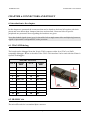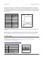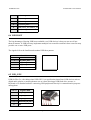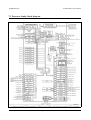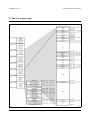
1
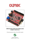
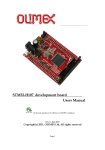
STM32-H407 development board USER’S MANUAL Revision A, July 2012 Designed by OLIMEX Ltd, 2012 All boards produced by Olimex LTD are ROHS compliant OLIMEX© 2012 STM32-H407 User's Manual DISCLAIMER © 2012 Olimex Ltd. Olimex®, logo and combinations thereof, are registered trademarks of Olimex Ltd. Other product names may be trademarks of others and the rights belong to their respective owners. The information in this document is provided in connection with Olimex products. No license, express or implied or otherwise, to any intellectual property right is granted by this document or in connection with the sale of Olimex products. The Hardware project is released under the Creative Commons Attribution-Share Alike 3.0 United States License. You may reproduce it for both your own personal use, and for commertial use. You will have to provide a link to the original creator of the project http://www.olimex.com on any documentation or website. You may also modify the files, but you must then release them as well under the same terms. Credit can be attributed through a link to the creator website: http://www.olimex.com The software is released under GPL. It is possible that the pictures in this manual differ from the latest revision of the board. The product described in this document is subject to continuous development and improvements. All particulars of the product and its use contained in this document are given by OLIMEX in good faith. However all warranties implied or expressed including but not limited to implied warranties of merchantability or fitness for purpose are excluded. This document is intended only to assist the reader in the use of the product. OLIMEX Ltd. shall not be liable for any loss or damage arising from the use of any information in this document or any error or omission in such information or any incorrect use of the product. This evaluation board/kit is intended for use for engineering development, demonstration, or evaluation purposes only and is not considered by OLIMEX to be a finished end-product fit for general consumer use. Persons handling the product must have electronics training and observe good engineering practice standards. As such, the goods being provided are not intended to be complete in terms of required design-, marketing-, and/or manufacturing-related protective considerations, including product safety and environmental measures typically found in end products that incorporate such semiconductor components or circuit boards. Olimex currently deals with a variety of customers for products, and therefore our arrangement with the user is not exclusive. Olimex assumes no liability for applications assistance, customer product design, software performance, or infringement of patents or services described herein. THERE IS NO WARRANTY FOR THE DESIGN MATERIALS AND THE COMPONENTS USED TO CREATE STM32-H407. THEY ARE CONSIDERED SUITABLE ONLY FOR STM32-H407. Page 2 of 32 OLIMEX© 2012 STM32-H407 User's Manual Table of Contents DISCLAIMER............................................................................................................. 2 CHAPTER 1 OVERVIEW......................................................................................... 5 1. Introduction to the chapter.......................................................................................................5 1.1 Features.....................................................................................................................................5 1.2 H407 or E407?..........................................................................................................................6 1.3 Target market and purpose of the board.............................................................................. 6 1.4 Organization.............................................................................................................................6 CHAPTER 2 SETTING UP THE STM32-H407 BOARD.......................................7 2. Introduction to the chapter.......................................................................................................7 2.1 Electrostatic warning...............................................................................................................7 2.2 Requirements........................................................................................................................... 7 2.3 Powering the board..................................................................................................................8 2.4 Prebuilt software......................................................................................................................8 CHAPTER 3 STM32-H407 BOARD DESCRIPTION............................................ 9 3. Introduction to the chapter.......................................................................................................9 3.1 Layout (top view).....................................................................................................................9 3.2 Layout (bottom view).............................................................................................................10 CHAPTER 4 THE STM32F407ZGT6 MICROCONTROLLER......................... 11 4. Introduction to the chapter.....................................................................................................11 4.1 The STM32F407ZGT6 features........................................................................................... 11 CHAPTER 5 CONTROL CIRCUITY AND HARDWARE MODULES.............13 5. Introduction to the chapter.....................................................................................................13 5.1 Reset........................................................................................................................................13 5.2 Clocks......................................................................................................................................13 5.3 Power supply circuit..............................................................................................................14 CHAPTER 6 CONNECTORS AND PINOUT....................................................... 15 6. Introduction to the chapter.....................................................................................................15 6.1 JTAG/SWD debug................................................................................................................. 15 6.2 SD/MMC slot..........................................................................................................................15 6.3 UEXT module.........................................................................................................................16 6.4 USB HOST..............................................................................................................................17 6.5 USB_OTG...............................................................................................................................17 6.6 Arduino platform...................................................................................................................18 6.7 20-pin connectors – PD – PE – PF - PG...............................................................................19 6.8 PWR Jack...............................................................................................................................20 6.9 Battery connector...................................................................................................................20 Page 3 of 32 OLIMEX© 2012 STM32-H407 User's Manual 6.10 U3BOOT...............................................................................................................................20 6.11 Jumper description..............................................................................................................20 6.11.1 PWR_SEL..........................................................................................................................21 6.11.2 B1_1/B1_0 and B0_1/B0_0...............................................................................................21 6.11.3 R-T......................................................................................................................................21 6.11.4 3.3V_E................................................................................................................................21 6.11.5 AGND_E............................................................................................................................22 6.11.6 AREF_EN..........................................................................................................................22 6.12 Additional hardware components...................................................................................... 22 CHAPTER 7 BLOCK DIAGRAM AND MEMORY.............................................23 7. Introduction to the chapter.....................................................................................................23 7.1 Processor family block diagram...........................................................................................24 7.2 Physical memory map........................................................................................................... 25 CHAPTER 8 SCHEMATICS...................................................................................26 8. Introduction to the chapter.....................................................................................................26 8.1 Eagle schematic......................................................................................................................26 8.2 Physical dimensions...............................................................................................................28 CHAPTER 9 REVISION HISTORY AND SUPPORT..........................................29 9. Introduction to the chapter.....................................................................................................29 9.1 Document revision................................................................................................................. 29 9.1 Board's revision......................................................................................................................29 9.3 Useful web links and purchase codes................................................................................... 30 9.3 Product support..................................................................................................................... 31 Page 4 of 32 OLIMEX© 2012 STM32-H407 User's Manual CHAPTER 1 OVERVIEW 1. Introduction to the chapter Thank you for choosing the STM32-H407 single board computer from Olimex! This document provides a user’s guide for the Olimex STM32-H407 board. As an overview, this chapter gives the scope of this document and lists the board’s features. The differences between the members of the OLIMEX STM32 F407 boards are mentioned. The document’s organization is then detailed. The STM32-H407 development board enables code development of applications running on the microcontroller STM32F407ZGT6, manufactured by STMicrocontrollers. 1.1 Features STM32F407ZGT6 Cortex-M4 210DMIPS, 1MB Flash, 196KB RAM, 3×12-bit 2.4 MSPS A/D, 2×12-bit D/A converters, USB OTG HS and USB OTG HS, Ethernet, 14 timers, 3 SPI, 3 I2C, Ethernet, 2 CANs, 3 12 bit ADCs, 2 12 bit DACs, 114 GPIOs, Camera interface JTAG connector with ARM 2x10 pin layout for programming/debugging UEXT connector USB host USB-OTG SD-card Input DCDC power supply which allows operation from 6-16VDC source Power and User LEDs Reset and User buttons Arduino shield platform with provided headers 4 full 20-pin Ports with the external memory bus for add-on modules PCB: FR-4, 1.5 mm (0,062"), soldermask, silkscreen component print Dimensions: 90x76 mm (3.54x3") Page 5 of 32 OLIMEX© 2012 STM32-H407 User's Manual 1.2 H407 or E407? The major difference between STM32-E407 and STM32-E407 is that the latter has built-in Ethernet (physical level transceiver Micrel - Micrel datasheet). STM32-E407 also features an extra USBOTG and a number of SMD jumpers on the bottom which help the user to control the multiplexing on some pins easier. STM32-E407 has 2 x USB-OTG both with a miniUSB interface. STM32H407 has 1 x USB-OTG and 1 x USB-HOST with the On-The-Go interfaced by miniUSB and the HOST by USB type A connector. If you need built-in Ethernet check the STM32-E407. 1.3 Target market and purpose of the board STM32-H407 is a development board featuring a powerful ARM Cortex-M4F microcontroller with the most important peripherals, interfaces and connectors mounted and ready to use. The board can be powered by a number of different sources, can be programmed via two different interfaces, has a TON of GPIO pins available on a number of headers. The board's Arduino platform headers give another option for enthusiasts who wish to implement support for Arduino/Maple/Pinguino shields giving the board additional features altogether with the option to add Olimex extension modules on the OLIMEX UEXT. All of the above options make the board quite versatile and suitable for numerous tasks and situations. The power of ARM and the creativity of OLIMEX come at the best price and the wellknown quality. Every ARM enthusiast would see STM32-H407 as an interesting bargain and quite capable board for its low price. 1.4 Organization Each section in this document covers a separate topic, organized as follow: – – Chapter 1 is an overview of the board usage and features Chapter 2 provides a guide for quickly setting up the board – – Chapter 3 contains the general board diagram and layout Chapter 4 describes the component that is the heart of the board: the STM32F207ZET6 microcontroller – Chapter 5 is an explanation of the control circuitry associated with the microcontroller to reset. Also shows the clocks on the board Chapter 6 covers the connector pinout, peripherals and jumper description – Page 6 of 32 OLIMEX© 2012 STM32-H407 User's Manual – – Chapter 7 shows the memory map Chapter 8 provides the schematics – Chapter 9 contains the revision history, useful links and support information Page 7 of 32 OLIMEX© 2012 STM32-H407 User's Manual CHAPTER 2 SETTING UP THE STM32-H407 BOARD 2. Introduction to the chapter This section helps you set up the STM32-H407 development board for the first time. Please consider first the electrostatic warning to avoid damaging the board, then discover the hardware and software required to operate the board. The procedure to power up the board is given, and a description of the default board behavior is detailed. 2.1 Electrostatic warning STM32-H407 is shipped in a protective anti-static package. The board must not be exposed to high electrostatic potentials. A grounding strap or similar protective device should be worn when handling the board. Avoid touching the component pins or any other metallic element. 2.2 Requirements In order to set up the STM32-H407 optimally, the following items are required: - JTAG or SWD interface programmer/debugger – can power the board and gives the ability to program/debug the board – to choose the correct programmer be sure that you are aware what software tools you are going to use when programming STM32-H407, and that the programmer supports STM32F407 processor. Additional components can be acquired in order to increase the functionality of the board: - External power supply - SD-card or USB-mini cable or extensive UEXT modules are recommended but not required - 3.7V Battery - MOD-XXXX boards for additional features on the UEXT (RTC, TC, GSM, MP3, RS-485 among others) – note that you will have to implement the software setup between the boards - Arduino/Maple/Pinguino shields – every shield is hardware compatible with H407 but will not work out-of-the-box, software implementation should be considered Some of the suggested items can be purchased by Olimex, for instance: Page 8 of 32 OLIMEX© 2012 STM32-H407 User's Manual ARM-USB-TINY-H – high-speed OpenOCD ARM JTAG debugger ARM-USB-OCD-H – high-speed OpenOCD ARM JTAG debugger with buffer protection USB-MINI-CABLE USBmini to USB-A cable - USB mini to USB-A cable BATTERY-LIPO1400MAH – lithium-polymer battery 1400mAh SY0612E - power supply adapter 12V/0.5A for iMX233-STM32-H407 2.3 Powering the board The board is powered in one of the following ways: 1)by PWR jack, 2)by JTAG/SWD programmer, 3)by USB-OTG. The PWR jack should be supplied from a 6V to 16V source with maximum current of 1A from the power jack. Without additional components and peripherals (no microSD card mounted, nothing connected to the USB, etc.) the typical consumption is 30mA @ 12V. For the European customers we sell an affordable power supply adapter 12V/0.5A - SY0612E. It is worth mentioning that the board can NOT be powered by the battery connector. The battery connected keeps some of the processor's functions remain intact (hibernate) during power down but it provides insufficient power for the board to operate properly. For example the RTC doesn't loose the values when there is a battery connected. 2.4 Prebuilt software Upon powering initially the board's red PWR LED and the green PWR LED should turn on. Page 9 of 32 OLIMEX© 2012 STM32-H407 User's Manual CHAPTER 3 STM32-H407 BOARD DESCRIPTION 3. Introduction to the chapter Here you get acquainted with the main parts of the board. Note the names used on the board differ from the names used to describe them. For the actual names check the STM32-H407 board itself. The board comes with a bag with 4 headers for the Arduino/Maple/Pinguino platform which were left unsoldered in case you don't wish to use those environments or you don't plan on using shields. There is also a bag of 4 rubber pads which can be placed in the 4 corner holes of the board. That way the board will be safe from short-circuiting on the bottom if placed on low-resistance surface. The placement stability of the board will also increase. 3.1 Layout (top view) Page 10 of 32 OLIMEX© 2012 STM32-H407 User's Manual 3.2 Layout (bottom view) On the bottom there are three tables printed – general jumper table, boot mode jumper table, power mode jumper table. The default positions of the tables are also shown. Page 11 of 32 OLIMEX© 2012 STM32-H407 User's Manual CHAPTER 4 THE STM32F407ZGT6 MICROCONTROLLER 4. Introduction to the chapter In this chapter is located the information about the heart of STM32-H407 – its Cortex-M4F microcontroller. The information is a modified version of the datasheet provided by its manufacturers from ST. 4.1 The STM32F407ZGT6 features Core: ARM 32-bit Cortex™-M4 CPU with FPU, Adaptive real-time accelerator (ART Accelerator™) allowing 0-wait state execution from Flash memory, frequency up to 168 MHz, memory protection unit, 210 DMIPS/1.25 DMIPS/MHz (Dhrystone 2.1), and DSP instructions Memories 1 Mbyte of Flash memory 192+4 Kbytes of SRAM including 64-Kbyte of CCM (core coupled memory) data RAM Flexible static memory controller supporting Compact Flash, SRAM, PSRAM, NOR and NAND memories LCD parallel interface, 8080/6800 modes Clock, reset and supply management 1.8 V to 3.6 V application supply and I/Os POR, PDR, PVD and BOR 4-to-26 MHz crystal oscillator Internal 16 MHz factory-trimmed RC (1% accuracy) 32 kHz oscillator for RTC with calibration Internal 32 kHz RC with calibration Sleep, Stop and Standby modes VBATsupply for RTC, 20×32 bit backup registers + optional 4 KB backup SRAM 3×12-bit, 2.4 MSPS A/D converters: 24 channels and 7.2 MSPS in triple interleaved mode 2×12-bit D/A converters General-purpose DMA: 16-stream DMA controller with FIFOs and burst support Up to 17 timers: up to twelve 16-bit and two 32-bit timers up to 168 MHz, each with up to 4 IC/OC/PWM or pulse counter and quadrature (incremental) encoder input Debug mode Serial wire debug (SWD) & JTAG interfaces Page 12 of 32 OLIMEX© 2012 STM32-H407 User's Manual Cortex-M4 Embedded Trace Macrocell™ 114 I/O ports with interrupt capability Up to 15 communication interfaces 3 × I2C interfaces (SMBus/PMBus) 4 USARTs/2 UARTs (10.5 Mbit/s, ISO 7816 interface, LIN, IrDA, modem control) 3 SPIs (37.5 Mbits/s), 2 with muxed full-duplex I2S to achieve audio class accuracy via internal audio PLL or external clock 2 × CAN interfaces (2.0B Active) SDIO interface Advanced connectivity USB 2.0 full-speed device/host/OTG controller with on-chip PHY USB 2.0 high-speed/full-speed device/host/OTG controller with dedicated DMA, onchip full-speed PHY and ULPI 10/100 Ethernet MAC with dedicated DMA: supports IEEE 1588v2 hardware, MII/RMII 8- to 14-bit parallel camera interface up to 54 Mbytes/s True random number generator CRC calculation unit 96-bit unique ID RTC: subsecond accuracy, hardware calendar For comprehensive information on the microcontroller visit the ST’s web page for a datasheet. At the moment of writing the microcontroller datasheet can be found at the following link: http://www.st.com/internet/com/TECHNICAL_RESOURCES/TECHNICAL_LITERATURE/DAT ASHEET/DM00037051.pdf Page 13 of 32 OLIMEX© 2012 STM32-H407 User's Manual CHAPTER 5 CONTROL CIRCUITY AND HARDWARE MODULES 5. Introduction to the chapter Here you can find information about reset circuit and quartz crystals locations, the power supply circuit is discussed. 5.1 Reset STM32-H407's reset circuit includes R21 (10KΩ), R19 (1 KΩ), C35 (100nF) and a RESET button. 5.2 Clocks There are two quartz crystals available on the board: 12 MHz quartz crystal Q1 is connected to pins 23 and 24 of the CORTEX-M4F processor. Quartz crystal Q2 is a 32 768Hz RTC (real-time clock) and is connected to pins 8 and 9. Page 14 of 32 OLIMEX© 2012 STM32-H407 User's Manual 5.3 Power supply circuit The power supply circuit of STM32-H407 allows flexible input supply from 6V to 16V direct current. This means a wide range of power supplies, adapters, converters are applicable. The maximum amperage the board can draw is 1A. The Li-Po battery connector cannot be used to fully power the board. It's function is to give an option to save internal data if the board needs to be relocated. It will keep the RTC alive, for instance. If you have successfully powered the board the red PWR LED will turn on. Note that it is possible to have the PWR LED on even if there isn't enough power for proper operation of the board and all the peripherals currently connected. Page 15 of 32 OLIMEX© 2012 STM32-H407 User's Manual CHAPTER 6 CONNECTORS AND PINOUT 6. Introduction to the chapter In this chapter are presented the connectors that can be found on the board all together with their pinout and notes about them. Jumpers functions are described. Notes and info on specific peripherals are presented. Notes regarding the interfaces are given. Note that slashed signals (xxxx/yyyy) in the tables below might mean either multiplexing between signals or port name correspondence on the processor. 6.1 JTAG/SWD debug The board can be debugged from the 20-pin JTAG connector either by a JTAG or a SWD compatible debugger. Below is the table of the JTAG. This interface can be used with the Olimex's OpenOCD debuggers. JTAG/SWD interface Pin # Signal Name Signal Name Pin # 1 +3.3V 11 - 2 +3.3V 12 GND 3 PB4/TRST 13 PB3/TDO 4 GND 14 GND 5 PA15/TDI 15 PB4/TRST 6 GND 16 GND 7 PA13/TMS 17 - 8 GND 18 GND 9 PA14/TCK 19 +5V_JTAG 10 GND 20 GND 6.2 SD/MMC slot The microSD card slot is a standard 8pin connector. Page 16 of 32 OLIMEX© 2012 STM32-H407 User's Manual We have tested a number of microSD cards on the STM32-H407 boards and all of them worked fine regardless manufacturer or capacity. However, keep in mind that some of the lower quality microSD cards might draw too much current from the slot which might cause power-state problems. If you suspect the microSD card is causing problems please try using another one of better quality for better results. microSD card connector Pin # Signal Name 1 DAT2/RES 2 CD/DAT3/CS 3 CMD/DI 4 VDD 5 SCL/SCLK 6 VSS 7 DAT0/RES 8 DAT1/RES Notice that the pad numeration is written at the bottom of STM32-H407 under the microSD card connector. When removing the card, please make sure that you release it from the connector by pushing and NOT by pulling the card directly (this can damage both the connector and the microSD card). 6.3 UEXT module STM32-H407 board has UEXT connector and can interface Olimex's UEXT modules. For more information on UEXT please visit: http://www.olimex.com/dev/OTHER/UEXT.pdf UEXT connector Pin # Signal Name 1 3.3V 2 GND 3 PC6/USART6_TX 4 PC7/USART6_RX Page 17 of 32 OLIMEX© 2012 STM32-H407 User's Manual 5 PB8/I2C1_SCL 6 PB9/I2C1_SDA 7 PC2/SPI2_MISO 8 PC3/SPI2_MOSI 9 PB10/SPI2_SCK/UART3_TX 10 PG10/UEXT_CS 6.4 USB HOST The big advantage of having USB hosts available over USB devices is that you can as well use them as masters. A USB host may implement multiple host controllers and each host controller may provide one or more USB ports. The signals follow the familiar and standard USB host pattern: USB 2-level host PIN# SIGNAL NAME 1 +5V_HOST_PWR 2 USB_HOST_D- 3 USB_HOST_D+ 4 GND 6.5 USB_OTG USB On-The-Go, often abbreviated USB OTG, is a specification that allows USB devices such as digital audio players or mobile phonesto act as a host allowing a USB flash drive, mouse, or keyboard to be attached and also connecting USB peripherals directly for communication purposes among them. Pin # Signal Name 1 +5V_OTG_PWR 2 USB_OTG_D- 3 USB_OTG_D+ 4 PB12/OTG_HS_ID 5 GND Page 18 of 32 OLIMEX© 2012 STM32-H407 User's Manual 6.6 Arduino platform The Arduino/Maple platform connectors (2x6pin and 2x8pin plastic headers) are not mounted but are included in the package. The reasons for not mounting the headers on the pin holes are two: first you might not need them if you do not wish to experiment with Arduino/Maple software; second there are two rows depending on the shield you might want to use the difference between the two rows is the distance between the two digital rows one is made according to the Arduino shield standard (e.g. you want to mount the row there if using Arduino certified shield), the other one is adjusted properly at 100mil step (e.g. you want to solder the digital pins here if using properly adjusted shields). The pinhole names are printed near the actual pinhole on the top of the board. Arduino platform pinholes CON1 CON2 Pin Signal Name Processor pin# Pin Signal Name Processor pin# RST RST 25 A0 PC0 26 3V3 3.3V - A1 PC1 27 5V 5V - A2 PB0 46 GND GND - A3 PB1 47 GND GND - A4 PC4 44 VIN VIN - A5 PC5 45 Arduino platform pinholes CON3 CON4 Pin Signal Name Processor pin# Pin Signal Name Processor pin# D0 PA3/USART_RX 37 D8 PA1 35 D1 PA2/USART_TX 36 D9 PB11 70 D2 PG7 92 D10 PA4 40 D3 PG8 93 D11 PA7 43 D4 PG12 127 D12 PA6 42 D5 PG13 128 D13 PA5 41 D6 PG14 129 GND AGND 31 D7 PG15 132 AREF AREF 32 Page 19 of 32 OLIMEX© 2012 STM32-H407 User's Manual 6.7 20-pin connectors – PD – PE – PF - PG The 4 20-pin connectors combine different processor ports and provide very nice GPIO option – you can use them with your breadboarding wires, you can mount headers, you can take measures, etc, etc. Note that all 4 headers come without connectors (unlike the UEXT or the JTAG) and connectors are not included in the package (unlike the Arduino platform). However they follow the standard 100mil step connectors – not hard to find and mount/solder if needed etc. PD Pin # PE Signal Name Pin # Signal Name Pin # Signal Name Pin # Signal Name 1 +3.3V 11 PD8 1 +3.3V 11 PE8 2 GND 12 PD9 2 GND 12 PE9 3 PD0 13 PD10 3 PE0 13 PE10 4 PD1 14 PD11 4 PE1 14 PE11 5 PD2 15 PD12 5 PE2 15 PE12 6 PD3 16 PD13 6 PE3 16 PE13 7 PD4 17 PD14 7 PE4 17 PE14 8 PD5 18 PD15 8 PE5 18 PE15 9 PD6 19 +5V 9 PE6 19 +5V 10 PD7 20 GND 10 PE7 20 GND PF Pin # Signal Name PG Pin # Signal Name Pin # Signal Name Pin # Signal Name 1 +3.3V 11 PF8 1 +3.3V 11 PG8 2 GND 12 PF9 2 GND 12 PG9 3 PF0 13 PF10 3 PG0 13 PG10 4 PF1 14 PF11 4 PG1 14 PG11 5 PF2 15 PF12 5 PG2 15 PG12 6 PF3 16 PF13 6 PG3 16 PG13 7 PF4 17 PF14 7 PG4 17 PG14 8 PF5 18 PF15 8 PG5 18 PG15 9 PF6 19 +5V 9 PG6 19 +5V 10 PF7 20 GND 10 PG7 20 GND Page 20 of 32 OLIMEX© 2012 STM32-H407 User's Manual 6.8 PWR Jack The power jack used is the typical 2.5mm one used by Olimex in most of our products. You should provide between 6 and 16 volts @ 1A to the board. Pin # Signal Name 1 Power Input 2 GND More info about the power supply can be found in chapters 2 and 5 of this manual. 6.9 Battery connector When using the battery connector keep in mind that it is an energy solution that wouldn't be able to power the board and all the peripherals! It help keeping information in the processor if you need to transport the board from one power supply to other. Pin # Signal Name 1 VBAT 2 GND The pin names are also written on the bottom of the board in the base of the connector. 6.10 U3BOOT U3BOOT are 3 pinholes set on USART3 and are named on the bottom – GND, RX, TX3 and notice there are two vias near them which are actually VCC and can be used if connecting U3BOOT. More information about booting over UART can be found in the processor's datasheet. 6.11 Jumper description Please note some of the jumpers on the board are SMD type. If you feel insecure in your soldering/cutting technique it is better not to try adjusting SMD jumpers. Page 21 of 32 OLIMEX© 2012 STM32-H407 User's Manual Also if you feel incapable of removing the PTH jumper with hand better use tweezers. We do. 6.11.1 PWR_SEL PWR_SEL is important PTH jumper allowing easy switching of input current. If you are powering the board via the PWR_JACK set it to position 1-2 (default → to the edge of the board). If powering from the JTAG/SWD set the jumper in position 3-4 (middle position). If powering from the USB-OTG set it in 5-6 position (to the tall capacitor C46) The default position is 1-2. 6.11.2 B1_1/B1_0 and B0_1/B0_0 B1_1/B1_0 and B0_1/B0_0 are PTH jumpers which can be moved relatively easy. Notice that these two jumpers must be moved together – they are responsible for the boot mode if bootloader is present. The board can search for bootloader on three places – User Flash Memory, System Memory or the Embedded SRAM. If B0_0 is closed the board will try to boot from User Flash Memory. If B0_1 is closed there are two variants depending on the state of B1_1/B1_0 jumper – if B0_1 is closed and B1_0 is closed the board will try to boot from System Memory. If B0_1 is closed and B1_1 is closed bootloader must be located in the Embedded SRAM. The default positions are B0_0 and B1_0 (Boot from User Flash Memory). 6.11.3 R-T This is SMD type jumper. If you close/solder this jumper RST and TRST at the JTAG will be connected. The default position is open/unsoldered. 6.11.4 3.3V_E This is SMD type jumper. Page 22 of 32 OLIMEX© 2012 STM32-H407 User's Manual Board digital power will be disabled if open/unsoldered The default position is closed. 6.11.5 AGND_E This is SMD type jumper. If open/unsoldered will disable analog ground. The default position is closed. 6.11.6 AREF_EN This is SMD type jumper. If open/unsoldered will disable ADC reference. The default position is closed. 6.12 Additional hardware components The components below are mounted on STM32-H407 but are not discussed above. They are listed here for completeness: Reset button - used for hardware reset of the board WKUP button – can be used as user button User LED + Power LED Page 23 of 32 OLIMEX© 2012 STM32-H407 User's Manual CHAPTER 7 BLOCK DIAGRAM AND MEMORY 7. Introduction to the chapter On the next page you can find a memory map for this family of processors. It is strongly recommended to refer to the original datasheet released by STMicroelectronics for one of higher quality. Page 24 of 32 OLIMEX© 2012 STM32-H407 User's Manual 7.1 Processor family block diagram Page 25 of 32 OLIMEX© 2012 STM32-H407 User's Manual 7.2 Physical memory map Page 26 of 32 OLIMEX© 2012 STM32-H407 User's Manual CHAPTER 8 SCHEMATICS 8. Introduction to the chapter In this chapter are located the schematics describing logically and physically STM32-H407. 8.1 Eagle schematic STM32-H407 schematic is visible for reference here. You can also find them on the web page for STM32-H407 at our site: https://www.olimex.com/dev/stm32-h407.html. They are located in HARDWARE section. The EAGLE schematic is situated on the next page for quicker reference. Page 27 of 32 130 120 94 83 61 51 16 38 107 3.3V_A C28 AREF_EN 1 C29 10uF/6.3V 3 2 1 3.3V 2 R16 AREF 100nF C30 15R Close 100nF VBAT R17 3.3V T 1107A-6_3.8_2.5 10k/1% 2 VCC BOOT0 4.7k R19 U6 NA RESET 1 3 GND RST 27pF C32 27pF 3.3V R25 R26 R28 NA NA NA +5V 1 3 5 7 9 11 13 15 17 19 2 4 6 8 10 12 14 16 18 20 R24 NA R27 R29 NA NA FSMC_A10 FSMC_A11 FSMC_A12 FSMC_A13 FSMC_A14 FSMC_A15 FSMC_INT2 PG1 PG3 PG5 PG7/D2 PG9 PG11 PG13/D5 PG15/D7 FSMC_NE2/FSMC_NCE3 FSMC_ NCE4 _1 /FSM C_ NCE3 FSMC_NCE4_2 ETH_RMII_TXD0 ETH_RMII_TXD1 FSMC_A0 FSMC_A1 FSMC_A2 FSMC_A3 FSMC_A4 FSMC_A5 FSMC_NIORD FSMC_NREG FSMC_NIOWR FSMC_CD FSMC_INTR PF 3.3V +5V 1 3 5 7 9 11 13 15 17 19 2 4 6 8 10 12 14 16 18 20 PF1 PF3 PF5 PF7 PF9 PF11 PF13 PF15 31 VSSA 6 VBAT R18 NA 24 FSMC_A6 FSMC_A7 FSMC_A8 FSMC_A9 NA(BH20S) 25 PG0 PG1 PG2 PG3 PG4 PG5 PG6 PG7/D2 PG8/D3 PG9 PG10 PG11 PG12/D4 PG13/D5 PG14/D6 PG15/D7 56 57 87 88 89 90 91 92 93 124 125 126 127 128 129 132 PF0 PF1 PF2 PF3 PF4 PF5 PF6 PF7 RF8 PF9 PF10 PF11 PF12 PF13 PF14 PF15 10 11 12 13 14 15 18 19 20 21 22 49 50 53 54 55 C10 47pF(NA) 100nF PC0/OTG_HS_ULPI_STP/ADC123_IN10 PC1/ETH_MDC/ADC123_IN11 PC2/SPI2_MISO/OTG_HS_ULPI_DIR/ETH_MII_TXD2/ADC123_IN12 PC3/SPI2_MOSI/I2S2_SD/OTG_HS_ULPI_NXT/ETH_MII_TX_CLK/ADC123_IN13 PC4/ETH_RMII_RX_D0/ETH_MII_RX_D0/ADC12_IN14 PC5/ETH_RMII_RX_D1/ETH_MII_RX_D1/ADC12_IN15 PC6/SPI2_MCK/TIM8_CH1/SDIO_D6/USART6_TX/DCMI_D0/TIM3_CH1 PC7/SPI3_MCK/TIM8_CH2/SDIO_D7/USART6_RX/DCMI_D1/TIM3_CH2 PC8/TIM8_CH3/SDIO_D0/TIM3_CH3/USART6_CK/DCMI_D2 PC9/I2S2_CKIN/I2S3_CKIN/MCO2/TIM8_CH4/SDIO_D1/I2C3_SDA/DCMI_D3/TIM3_CH4 PC10/SPI3_SCK/I2S3_CK/UART4_TX/SDIO_D2/DCMI_D8/USART3_TX PC11/UART4_RX/SPI3_MISO/SDIO_D3/DCMI_D4/USART3_RX PC12/UART5_TX/SDIO_CK/DCMI_D9/SPI3_MOSI/I2S3_SD/USART3_CK PC13/RTC_AF1 PC14/OSC32_IN PC15/OSC32_OUT BOOT0/VPP PH0/OSC_IN PH1/OSC_OUT NRST PG0/FSMC_A10 PG1/FSMC_A11 PG2/FSMC_A12 PG3/FSMC_A13 PG4/FSMC_A14 PG5/FSMC_A15 PG6/FSMC_INT2 PG7/FSMC_INT3/USART6_CK PG8/USART6_RTS/ETH_PPS_OUT PG9/USART6_RX/FSMC_NE2/FSMC_NCE3 PG10/FSMC_NCE4_1/FSMC_NE3 PG11/FSMC_NCE4_2/ETH_MII_TX_EN PG12/FSMC_NE4/USART6_RTS PG13/FSMC_A24/USART6_CTS/ETH_MII_TXD0/ETH_RMII_TXD0 PG14/FSMC_A25/USART6_TX/ETH_MII_TXD1/ETH_RMII_TXD1 PG15/USART6_CTS/DCMI_D13 PD0/FSMC_D2/CAN1_RX PD1/FSMC_D3/CAN1_TX PD2/TIM3_ETR/UART5_RX/SDIO_CMD/DCMI_D11 PD3/FSMC_CLK/USART2_CTS PD4/FSMC_NOE/USART2_RTS PD5/FSMC_NWE/USART2_TX PD6/FSMC_NWAIT/USART2_RX PD7/USART2_CK/FSMC_NE1/FSMC_NCE2 PD8/FSMC_D13/USART3_TX PD9/FSMC_D14/USART3_RX PD10/FSMC_D15/USART3_CK PD11/FSMC_A16/USART3_CTS PD12/FSMC_A17/TIM4_CH1/USART3_RTS PD13/FSMC_A18/TIM4_CH2 PD14/FSMC_D0/TIM4_CH3 PD15/FSMC_D1/TIM4_CH4 PF0/FSMC_A0/I2C2_SDA PF1/FSMC_A1/I2C2_SCL PF2/FSMC_A2/I2C2_SMBA PF3/FSMC_A3/ADC3_IN9 PF4/FSMC_A4/ADC3_IN14 PF5/FSMC_A5/ADC3_IN15 PF6/TIM10_CH1/FSMC_NIORD/ADC3_IN4 PF7/TIM11_CH1/FSMC_NREG/ADC3_IN5 PF8/TIM13_CH1/FSMC_NIOWR/ADC3_IN6 PF9/TIM14_CH1/FSMC_CD/ADC3_IN7 PF10/FSMC_INTR/ADC3_IN8 PF11/DCMI_12 PF12/FSMC_A6 PF13/FSMC_A7 PF14/FSMC_A8 PF15/FSMC_A9 PE0/TIM4_ETR/FSMC_NBL0/DCMI_D2 PE1/FSMC_NBL1/DCMI_D3 PE2/TRACECK/FSMC_A23/ETH_MII_TXD3 PE3/TRACED0/FSMC_A19 PE4/TRACED1/FSMC_A20/DCMI_D4 PE5/TRACED2/FSMC_A21/TIM9_CH1/DCMI_D6 PE6/TRACED3/FSMC_A22/TIM9_CH2/DCMI_D7 PE7/FSMC_D4/TIM1_ETR PE8/FSMC_D5/TIM1_CH1N PE9/FSMC_D6/TIM1_CH1 PE10/FSMC_D7/TIM1_CH2N PE11/FSMC_D8/TIM1_CH2 PE12/FSMC_D9/TIM1_CH3N PE13/FSMC_D10/TIM1_CH3 PE14/FSMC_D11/TIM1_CH4 PE15/FSMC_D12/TIM1_BKIN 34 35 36 37 40 41 42 43 100 101 102 103 104 105 109 110 PA0/WKUP PA1/D8 PA2/USART2_TX PA3/USART2_RX PA4/D10/SPI1_NSS PA5/D13/SPI1_SCK PA6/D12/SPI1_MISO PA7/D11/SPI1_MOSI PA8/USB_HS_VBUSON PA9/OTG_FS_VBUS PA10/USB_FS_VBUSON PA11/OTG_FS_DM PA12/OTG_FS_DP PA13/TMS PA14/TCK PA15/TDI 46 47 48 133 134 135 136 137 139 140 69 70 73 74 75 76 PB0/A2 PB1/A3 PB2 PB3/TDO PB4/TRST PB5/USB_HS_FAULT PB6/USB_FS_FAULT RB7/UEXT_CS PB8/I2C1_SCL PB9/I2C1_SDA PB10/SPI2_SCK/UART3_TX RB11/D9/UART3_RX PB12/OTG_HS_ID PB13/OTG_HS_VBUS PB14/OTG_HS_DM PB15/OTG_HS_DP 26 27 28 29 44 45 96 97 98 99 111 112 113 7 8 9 PC0/A0 PC1/A1 PC2/SPI2_MISO PC3/SPI2_MOSI PC4/A4 PC5/A5 PC6/USART6_TX PC7/USART6_RX PC8/SD_D0 PC9/SD_D1 PC10/SD_D2 PC11/SD_D3 PC12/SD_CLK LED R22 B1_1/B1_0 3.3V 141 142 1 2 3 4 5 58 59 60 63 64 65 66 67 68 PE0 PE1 PE2 PE3 PE4 PE5 PE6 PE7 PE8 PE9 PE10 PE11 PE12 PE13 PE14 PE15 GND_PIN C48 C49 10nF 3.3nF MP1482DS R40 2.2k L5 10uH/2.3A/YS75/7x8 +5V_OTG_PWR +5V_JTAG +5V_EXT 5 3 1 6 4 2 4 1 HN2x3(1-2:Close) R42 4.99k/1% R41 1.1k/1% C43 C50 22uF/6.3V C51 22uF/6.3V 100uF/16V/mini 3.3V 2 C39 22uF/6.3V U7 IN LX EN FB 3 3.3V PD0 PD2/SD_ CMD PD4 PD6 PD8 PD10 PD12 PD14 FSMC_NBL0 FSMC_NBL1 FSMC_A23 FSMC_A19 FSMC_A20 FSMC_A21 FSMC_A22 FSMC_D4 FSMC_D5 FSMC_D6 FSMC_D7 FSMC_D8 FSMC_D9 FSMC_D10 FSMC_D11 FSMC_D12 PE0 PE2 PE4 PE6 PE8 PE10 PE12 PE14 C38 R38 1.1k/1% 22uF/6.3V C41 22uF/6.3V C44 C42 220uF/16V/mini 100nF AGND_E 2 1 Close Page 28 of 32 BH10R 2 4 6 8 10 1 3 USB 3.3V R31 4.7k PC7/USART6_RX PB9/I2C1_SDA PC3/SPI2_MOSI RB7/UEXT_CS 2 4 6 8 10 12 14 16 18 20 R23 5 7 NA 9 11 13 15 17 19 1 3 5 7 9 11 13 15 17 19 3.3V +5V R32 47k/1% PD1 PD3 PD5 PD7 PD9 PD11 PD13 PD15 2 4 6 8 10 12 14 16 18 20 PE1 PE3 PE5 PE7 PE9 PE11 PE13 PE15 NA(BH20S) 1 USART3_TX 2 USART3_RX 3 GND NA(HN1X3) U3BOOT WKUP 2 T 11 07 A-6 _ 3 .8 _ 2 .5 R34 1k C40 D8 D9 D10 D11 D12 D13 GND AREF 100nF 1 3 5 7 9 PB10 /SPI2 _ SCK/UART3 _T X RB11 /D9 /UART3 _RX 3.3V_E R33 4.99k/1% D0 D1 D2 D3 D4 D5 D6 D7 NA(BH20S) PE Close 22pF C36 +5V 3.3V 5 GND SY8008C(AA)C A0 A1 A2 A3 A4 A5 USB-OTG PD FSMC_CLK FSMC_NOE FSMC_NWE FSMC_NWAIT FSMC_NE1 FSMC_D13 FSMC_D14 FSMC_D15 FSMC_A16 FSMC_A17 FSMC_A18 FSMC_D0 FSMC_D1 1 1 2 3 4 5 6 7 8 UEXT PC6/USART6_TX PB8/I2C1_SCL PC2/SPI2_MISO PB10/SPI2_SCK/UART3_TX RST 3V3 5V GND GND VIN CON4 NA(PN1X8) 3.3V LED/RED /0603 1 3 5 6 NA(PN1X8) R30 4.7k Q2 C33 32768Hz/6pF 15pF C34 15pF FSMC_D2 FSMC_D3 1 2 3 4 5 6 7 8 PA1/D8 RB11/D9/UART3_RX PA4/D10/SPI1_NSS PA7/D11/SPI1_MOSI PA6/D12/SPI1_MISO PA5/D13/SPI1_SCK AGND AREF ETH_RMII_RXD0 ETH_RMII_RXD1 PW R _L E D IN BS EN SW SS FB GND COMP 1 2 3 4 5 6 USART3_TX USART3_RX ETH_RMII_MDC L6 2.2uH/3A/YS75/7x8 + 2 7 8 4 + 1 0 0 n FC 4 7 +C 4 6 D4 SMBJ16A 470uF /25V/LOWESR/105C U8 47k NA(PN1X6) CON2 PA3/USART2_RX PA2/USART2_TX PG7/D2 PG8/D3 PG12/D4 PG13/D5 PG14/D6 PG15/D7 3.3V PWR_SEL VIN PC0/A0 PC1/A1 PB0/A2 PB1/A3 PC4/A4 PC5/A5 NA(PN1X6) CON3 R15 4.7k ETH_RMII_TX_EN U4 1 2 3 4 5 6 3.3V +5V HN1x3(B1_1:Open;B1_0:Close) GN D PD0 PD1 PD2/SD_CMD PD3 PD4 PD5 PD6 PD7 PD8 PD9 PD10 PD11 PD12 PD13 PD14 PD15 L3 3.3V ETH_RMII_CRS_DV VBUS DD+ ID GND FB 0805/600R/200mA(201209-601) RST ETH_RMII_REF_CLK ETH_RMII_MDIO ETH_RMII_MDINT NA 114 115 116 117 118 119 122 123 77 78 79 80 81 82 85 86 +5V_OTG_PWR USB_OTG_DUSB_OTG_D+ PB12/OTG_HS_ID CON1 +5V R39 1 0 0 n FC 4 C11 POWER SUPPLY CIRCUIT VIN PWR_JACK YDJ-1136 USB_OTG +5V_OTG_PWR USB_OTG_DUSB_OTG_D+ PB12/OTG_HS_ID D2 USB_A_VERTICAL USB_OTG 1 00 u F/3 5 V/L OWESR/1 05 C/6 .3 x11 mm _RM 2.5 PB0/TIM3_CH3/TIM8_CH2N/OTG_HS_ULPI_D1/ETH_MII_RXD2/TIM1_CH2N/ADC12_IN8 PB1/TIM3_CH4/TIM8_CH3N/OTG_HS_ULPI_D2/ETH_MII_RXD3/OTG_HS_INTN/TIM1_CH3N/ADC12_IN9 PB2/BOOT1 PB3/JTDO/TRACESWO/SPI3_SCK/I2S3_CK/TIM2_CH2/SPI1_SCK PB4/NJTRST/SPI3_MISO/TIM3_CH1/SPI1_MISO PB5/I2C1_SMBA/CAN2_RX/OTG_HS_ULPI_D7/ETH_PPS_OUT/TIM3_CH2/SPI1_MOSI/SPI3_MOSI/DCMI_D10/I2S3_SD PB6/I2C1_SCL/TIM4_CH1/CAN2_TX/OTG_FS_INTN/DCMI_D5/USART1_TX PB7/I2C1_SDA/FSMC_NL/DCMI_VSYNC/USART1_RX/TIM4_CH2 PB8/TIM4_CH3/SDIO_D4/TIM10_CH1/DCMI_D6/OTG_FS_SCL/ETH_MII_TXD3/I2C1_SCL/CAN1_RX PB9/SPI2_NSS/I2S2_WS/TIM4_CH4/TIM11_CH1/OTG_FS_SDA/SDIO_D5/DCMI_D7/I2C1_SDA/CAN1_TX PB10/SPI2_SCK/I2S2_CK/I2C2_SCL/USART3_TX/OTG_HS_ULPI_D3/ETH_MII_RX_ER/OTG_HS_SCL/TIM2_CH3 PB11/I2C2_SDA/USART3_RX/OTG_HS_ULPI_D4/ETH_RMII_TX_EN/ETH_MII_TX_EN/OTG_HS_SDA/TIM2_CH4 PB12/SPI2_NSS/I2S2_WS/I2C2_SMBA/USART3_CK/TIM1_BKIN/CAN2_RX/OTG_HS_ULPI_D5/ETH_RMII_TXD0/ETH_MII_TXD0/OTG_HS_ID PB13/SPI2_SCK/I2S2_CK/USART3_CTS/TIM1_CH1N/CAN2_TX/OTG_HS_ULPI_D6/ETH_RMII_TXD1/ETH_MII_TXD1/OTG_HS_VBUS PB14/SPI2_MISO/TIM1_CH2N/TIM12_CH1/OTG_HS_DM/USART3_RTS/TIM8_CH2N PB15/SPI2_MOSI/I2S2_SD/TIM1_CH3N/TIM8_CH3N/TIM12_CH2/OTG_HS_DP 6-16VD C MIC2026-1YM 3.3V NA(ESDA6V1L) PA0/WKUP/USART2_CTS/USART4_TX/ETH_MII_CRS/TIM2_CH1_ETR/TIM5_CH1/TIM8_ETR/ADC123_CH0 PA1/USART2_RTS/USART4_RX/ETH_RMII_REF_CLK/ETH_MII_RX_CLK/TIM5_CH2/TIM2_CH2/ADC123_IN1 PA2/USART2_TX/TIM5_CH3/TIM9_CH1/TIM2_CH3/ETH_MDIO/ADC123_IN2 PA3/USART2_RX/TIM5_CH4/TIM9_CH2/TIM2_CH4/OTG_HS_ULPI_D0/ETH_MII_COL/ADC123_IN3 PA4/SPI1_NSS/SPI3_NSS/USART2_CK/DCMI_HSYNC/OTG_HS_SOF/I2S3_WS/ADC12_IN4/DAC1_OUT PA5/SPI1_SCK/OTG_HS_ULPI_CK/TIM2_CH1_ETR/TIM8_CHIN/ADC12_IN5/DAC2_OUT PA6/SPI1_MISO/TIM8_BKIN/TIM13_CH1/DCMI_PIXCLK/TIM3_CH1/TIM1_BKIN/ADC12_IN6 PA7/SPI1_MOSI/TIM8_CH1N/TIM14_CH1/TIM3_CH2/ETH_MII_RX_DV/TIM1_CH1N/RMII_CRS_DV/ADC12_IN7 PA8/MCO1/USART1_CK/TIM1_CH1/I2C3_SCL/OTG_FS_SOF PA9/USART1_TX/TIM1_CH2/I2C3_SMBA/DCMI_D0/OTG_FS_VBUS PA10/USART1_RX/TIM1_CH3/OTG_FS_ID/DCMI_D1 PA11/USART1_CTS/CAN1_RX/TIM1_CH4/OTG_FS_DM PA12/USART1_RTS/CAN1_TX/TIM1_ETR/OTG_FS_DP PA13/JTMS-SWDIO PA14/JTCK-SWCLK PA15/JTDI/SPI3_NSS/I2S3_WS/TIM2_CH1_ETR/SPI1_NSS VSS_11 VSS_10 VSS_9 VSS_8 VSS_7 VSS_6 VSS_5 VSS_4 VSS_2 VREF+ C9 PB12/OTG_HS_ID VCAP_2 32 5 6 33k 33k SHIELD FB 0805/600R/200mA(201209-601) GND1 15R 3 2 1 8 7 6 5 USB GND2 R10 RM4G2 RM4G1 NA(USBLC6-2P6) ENA OUT_A FLAG_A IN FLAG_B GND ENB OUT_B GND4 PB14/OTG_HS_DM 1 2 3 4 GND3 0R(board_mounted) 3.3V U3 15R 4 0R U2 3.3V 1 2 3 4 L2 PO W E R R9 C8 33k 33k 1 0 0 n FC 1 2 R8 PB15/OTG_HS_DP 47pF(NA) VCAP_1 VDDA 138 RST 100nF NA(BH20S) PF0 PF2 PF4 PF6 RF8 PF10 PF12 PF14 R20 150R C35 PG PG0 PG2 PG4 PG6 PG8/D3 PG10 PG12/D4 PG14/D6 MICRO RM4G4 RM4G3 NA(ESDA6V1L) PA10/USB_FS_VBUSON PB6/USB_FS_FAULT PB5/USB_HS_FAULT PA8/USB_HS_VBUSON PB13/OTG_HS_VBUS 22uF/6.3V VDD_1 VDD_2 VDD_3 VDD_4 VDD_5 VDD_6 VDD_7 VDD_8 VDD_9 VDD_10 VDD_11 VDD_12 VDD_SA 33 23 Q12 .00 0 M Hz/HC-4 9 SM (SM D)/2 0p F 1k RESET C31 Q1 R21 CD/DAT3/CS CMD/DI VSS VDD CLK/SCLK DAT0/DO DAT1/RES DAT2/RES +5V N A (2 xP N 1 x6 _ 2 xP N 1 x8 ) 106 100nF NA(USBLC6-2P6) 10 0u F/3 5 V/L OWESR/1 05 C/6.3 x11 m m_RM 2.5 AN AL O G 71 47pF(NA) USB_HOST +5V_HOST_PWR USB_HOST_DUSB_HOST_D+ C3 D1 D IG ITAL C13 2.2uF/6.3V C27 2.2uF/6.3V C5 ARDUINO: SH PLATFORM 1 0 0 n FC 2 6 1 0 0 n FC 2 5 1 0 0 n FC 24 1 0 0 n FC 2 3 1 0 0 n FC 2 2 1 00 n FC 2 1 1 0 0 n FC 2 0 1 0 0 n FC 1 9 C 18 1 0 u F/6.3 V R11 0 R (b o a rd _ mo u nte d ) 0R C17 1 0 u F/6 .3 V 1 0 0 n FC 1 6 C 15 1 0 u F/6 .3 V 72 108 143 39 17 52 62 84 95 121 131 30 144 C2 +5V_HOST_PWR USB_HOST_DUSB_HOST_D+ 1 2 3 PA10/USB_FS_VBUSON PB6/USB_FS_FAULT PB5/USB_HS_FAULT PA8/USB_HS_VBUSON U5 STM32F407ZGT6 R14 NA B0_1/B0_0 HN1x3(B0_1:Open;B0_0:Close) 47pF(NA) R7 1M SD/MMC USB_HOST U1 6 5 4 D IG ITAL WF2S C14 1 0 u F/6 .3 V L4 FB 0 8 0 5 /6 0 0 R /2 0 0 mA (2 0 1 2 0 9 -6 0 1 ) 1 2 C1 C45 22uF/6.3V 3V_BAT 15R SD/MMC CARD JTAG BAT54C D3 R4 + 33 k 33k L1 R M1 G 3 R M1G 2 C7 3.3V R3 NA 2 3 6 4 5 7 8 1 PC12/SD_CLK PC8/SD_D0 PC9/SD_D1 PC10/SD_D2 R-T 0R(board_mounted) 100nF C6 PB3/TDO RST 15R PA12/OTG_FS_DP 0R 3.3V PC11/SD_D3 PD2/SD_CMD PB4/TRST 1 R2 + NA(10k) 2 R1 PA11/OTG_FS_DM N A(1 0 k ) N A(1 0 k ) 10k 10k PA9/OTG_FS_VBUS R12 R13 10k RM2G2 RM3G2 RM3G1 PB4/TRST PA15/TDI PA13/TMS PA14/TCK 3.3V 3 RM3G3 R6 NA RM2G3 NA(10k) 3.3V 3.3V 2 +5V_JTAG RM2G1 NA(10k) R M1 G 1 RM2G4 NA(10k) 3.3V 1 1 3 5 7 9 11 13 15 17 19 R5 NA 3.3V CL470nH/0805/1.76R/250mA 2 4 6 8 10 12 14 16 18 20 JTAG BH20R 3.3V R M1 G 4 3.3V 33k STM32-H407 User's Manual 33k OLIMEX© 2012 BUTTON and LED 3.3V R35 1k C37 100nF R36 1k R37 47k/1% PA0/WKUP STM32-H407_Rev_B1 OLIMEX LTD PLOVDIV http://www.olimex.com LED LED/GREEN/0603 LED OLIMEX© 2012 STM32-H407 User's Manual 8.2 Physical dimensions Note that all dimensions are in millimeters. The three highest elements on the board in order from the tallest to the shortest are: capacitor C46 – 17.2mm (0.677'') over the pcb; USB host connectors – 14.3mm (0.563''); capacitators C11 and C3 – 11.5mm (0.453''). Note that the above measures does not include the PCB. Page 29 of 32 OLIMEX© 2012 STM32-H407 User's Manual CHAPTER 9 REVISION HISTORY AND SUPPORT 9. Introduction to the chapter In this chapter you will find the current and the previous version of the document you are reading. Also the web-page for your device is listed. Be sure to check it after a purchase for the latest available updates and examples. 9.1 Document revision Revision, Date Changes Modified Page# A, 20.07.12 Initial Creation All B, 25.07.12 Page 6 - Added comparison details Page 16 - Table error 6 16 9.1 Board's revision Revision, Date B1, 07.06.12 Revision Notes Initial release Page 30 of 32 OLIMEX© 2012 STM32-H407 User's Manual 9.3 Useful web links and purchase codes The web page you can visit for more info on your device is https://www.olimex.com/dev/stm32h407.html. You can get the latest updates on the software at: https://github.com/OLIMEX/STM32F4. ORDER CODES: STM32-H407 – the version of the board discussed in this document STM32-E407 – the version of the board featuring Ethernet ARM-USB-TINY-H – OpenOCD compatible high-speed debugger/programmer with JTAG interface ARM-USB-OCD-H – OpenOCD compatible debugger/programmer with JTAG interface, protection buffers and better power supply circuit SY0612E - power supply adapter 12V/0.5A for STM32-H407 – 220V (European compatibility) The latest price list can be found at http://olimex.com/dev/pricelist.html. How to order? You can order to us directly or by any of our distributors. Check http://www.olimex.com/ and http://olimex.com/dev/order.html for more info. Page 31 of 32 OLIMEX© 2012 STM32-H407 User's Manual 9.3 Product support For product support, hardware information and error reports mail to: [email protected]. Note that we are primarily a hardware company and our software support is limited. Please consider reading the paragraph below about the warranty of Olimex products. Warranty and returns: Our boards have lifetime warranty against manufacturing defects and components. During development work it is not unlikely that you can burn your programmer or development board. This is normal, we also do development work and we have damaged A LOT of programmers and boards during our daily job so we know how it works. If our board/programmer has worked fine then stopped, please check if you didn't apply over voltage by mistake, or shorted something in your target board where the programmer was connected etc. Sometimes boards might get damaged by ESD shock voltage or if you spill coffee on them during your work when they are powered. Please note that warrany do not cover problems caused by unproper use, shorts, over-voltages, ESD shock etc. If the board has warranty label it should be not broken. Broken labels void the warranty, same applies for boards modified by the customer, for instance soldering additional components or removing components - such boards will be not be a subject of our warranty. If you are positive that the problem is due to manufacturing defect or component you can return the board back to us for inspection. When we receive the board we will check and if the problem is caused due to our fault and we will repair/replace the faulty hardware free of charge, otherwise we can quote price of the repair. Note that all shippings back and forth have to be covered by the customer. Before you ship anything back you need to ask for RMA. When you ship back please attach to it your shipping address, phone, e-mail, RMA# and brief description of the problem. All boards should be sent back in antistatic package and well packed to prevent damages during the transport. Page 32 of 32