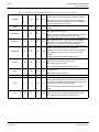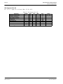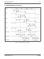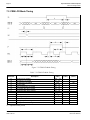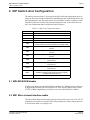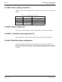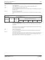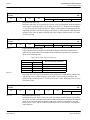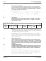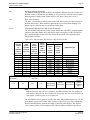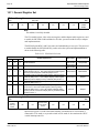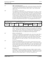
1
SPC8100 Low Power LCD VGA Controller
SPC8100
TECHNICAL MANUAL
Document Number: X03A-Q-001-01
Copyright © 1999 Epson Research and Development, Inc. All Rights Reserved.
Information in this document is subject to change without notice. You may download and use this document, but only for your own use in
evaluating Seiko Epson/EPSON products. You may not modify the document. Epson Research and Development, Inc. disclaims any
representation that the contents of this document are accurate or current. The Programs/Technologies described in this document may contain
material protected under U.S. and/or International Patent laws.
EPSON is a registered trademark of Seiko Epson Corporation. All other trademarks are the property of their respective owners.
Page 2
Epson Research and Development
Vancouver Design Center
THIS PAGE LEFT BLANK
SPC8100
X03A-Q-001-01
TECHNICAL MANUAL
Issue Date: 99/03/29
Epson Research and Development
Vancouver Design Center
Page 3
COMPREHENSIVE SUPPORT TOOLS
EPSON provides the designer and manufacturer a complete set of resources and tools for the development of LCD
Graphics Systems.
Documentation
• Technical manuals
• Evaluation/Demonstration board manual
Evaluation/Demonstration Board
•
•
•
•
•
•
Assembled and fully tested Graphics Evaluation/Demonstration board
Schematic of Evaluation/Demonstration board
Parts List
Installation Guide
CPU Independent Software Utilities
Evaluation Software
Application Engineering Support
EPSON offers the following services through their Sales and Marketing Network:
• Sales Technical Support
• Customer Training
• Design Assistance
Application Engineering Support
Engineering and Sales Support is provided by:
Japan
Seiko Epson Corporation
Electronic Devices Marketing Division
421-8, Hino, Hino-shi
Tokyo 191-8501, Japan
Tel: 042-587-5812
Fax: 042-587-5564
http://www.epson.co.jp
Hong Kong
Epson Hong Kong Ltd.
20/F., Harbour Centre
25 Harbour Road
Wanchai, Hong Kong
Tel: 2585-4600
Fax: 2827-4346
TECHNICAL MANUAL
Issue Date: 99/03/29
North America
Epson Electronics America, Inc.
150 River Oaks Parkway
San Jose, CA 95134, USA
Tel: (408) 922-0200
Fax: (408) 922-0238
http://www.eea.epson.com
Taiwan, R.O.C.
Epson Taiwan Technology
& Trading Ltd.
10F, No. 287
Nanking East Road
Sec. 3, Taipei, Taiwan, R.O.C.
Tel: 02-2717-7360
Fax: 02-2712-9164
Europe
Epson Europe Electronics GmbH
Riesstrasse 15
80992 Munich, Germany
Tel: 089-14005-0
Fax: 089-14005-110
Singapore
Epson Singapore Pte., Ltd.
No. 1
Temasek Avenue #36-00
Millenia Tower
Singapore, 039192
Tel: 337-7911
Fax: 334-2716
SPC8100
X03A-Q-001-01
Page 4
Epson Research and Development
Vancouver Design Center
THIS PAGE LEFT BLANK
SPC8100
X03A-Q-001-01
TECHNICAL MANUAL
Issue Date: 99/03/29
Epson Research and Development
Vancouver Design Center
Page 5
Table of Contents
SPECIFICATION
SPC8100 Hardware Functional Specification
UTILITIES
CONFIG Configuration Utility
PS Power Save Utility
RAMBIOS Utility
VCDISP Display Utility
VCMODE Display Utility
DRIVERS
SPC8100 Windows v3.0 Display Drivers
SPC8100 OS/2 Display Drivers
EVALUATION
SDU8100B0B Rev. 2.1 Evaluation Board User Manual
TECHNICAL MANUAL
Issue Date: 99/03/29
SPC8100
X03A-Q-001-01
Page 6
Epson Research and Development
Vancouver Design Center
THIS PAGE LEFT BLANK
SPC8100
X03A-Q-001-01
TECHNICAL MANUAL
Issue Date: 99/03/29
SPC8100 Low Power LCD VGA Controller
Hardware Functional Specification
Document Number: X03A-A-001-01
Copyright © 1999 Epson Research and Development, Inc. All Rights Reserved.
Information in this document is subject to change without notice. You may download and use this document, but only for your own use in
evaluating Seiko Epson/EPSON products. You may not modify the document. Epson Research and Development, Inc. disclaims any
representation that the contents of this document are accurate or current. The Programs/Technologies described in this document may contain
material protected under U.S. and/or International Patent laws.
EPSON is a registered trademark of Seiko Epson Corporation. All other trademarks are the property of their respective owners.
VGA, EGA, CGA, MDA, PC/XT/AT, MicroChannel, IBM are registered trademarks of IBM.
Hercules is a registered trademark of Hercules Computer Technology.
Page 2
Epson Research and Development
Vancouver Design Center
THIS PAGE LEFT BLANK
SPC8100
X03A-A-001-01
Hardware Functional Specification
Issue Date: 99/02/17
Epson Research and Development
Vancouver Design Center
Page 3
Table of Contents
1
Introduction . . . . . . . . . . . . . . . . . . . . . . . . . . . . . . . . . . . . . . . 11
1.1 Scope . . . . . . . . . . . . . . . . . . . . . . . . . . . . . . . . . . 11
1.2 Overview Description . . . . . . . . . . . . . . . . . . . . . . . . . . . 11
2
Features . . . . . . . . . . . . . .
2.1 Technology . . . . . . . .
2.2 Display Memory Configuration
2.3 System . . . . . . . . . .
2.4 Display Technologies Supported
3
Typical System Implementation . . . . . . . . . . . . . . . . . . . . . . . . . . . . 14
3.1 Block Diagram . . . . . . . . . . . . . . . . . . . . . . . . . . . . . . 14
3.2 Typical System Implementation . . . . . . . . . . . . . . . . . . . . . . . 15
4
Internal Description . . . . . . . .
4.1 Functional Block Diagram . . .
4.2 Functional Block Descriptions . .
4.2.1 Sequencer . . . . . . . . . .
4.2.2 CRT Controller . . . . . . .
4.2.3 Address Generator . . . . . .
4.2.4 Attributes Controller . . . .
4.2.5 Graphics Controller . . . . .
4.2.6 Memory Decoder . . . . . .
4.2.7 Port Decoder . . . . . . . . .
4.2.8 Auxiliary Ports . . . . . . .
4.2.9 CGA Ports . . . . . . . . . .
4.2.10 VGA/EGA Ports . . . . . . .
4.2.11 Hercules/MDA Ports . . . .
4.2.12 Display Control Ports . . . .
4.2.13 Clock Generation . . . . . .
4.2.14 LCD Interface Logic . . . .
4.2.15 RAMDAC . . . . . . . . . .
. . . .
. . . .
. . . .
. . . . .
. . . . .
. . . . .
. . . . .
. . . . .
. . . . .
. . . . .
. . . . .
. . . . .
. . . . .
. . . . .
. . . . .
. . . . .
. . . . .
. . . . .
. . .
. .
. .
. . .
. . .
. . .
. . .
. . .
. . .
. . .
. . .
. . .
. . .
. . .
. . .
. . .
. . .
. . .
.
.
.
.
.
.
.
.
.
.
.
.
.
.
.
.
.
.
. . . . . .
. . . . .
. . . . .
. . . . . . .
. . . . . . .
. . . . . . .
. . . . . . .
. . . . . . .
. . . . . . .
. . . . . . .
. . . . . . .
. . . . . . .
. . . . . . .
. . . . . . .
. . . . . . .
. . . . . . .
. . . . . . .
. . . . . . .
.
.
.
.
.
.
.
.
.
.
.
.
.
.
.
.
.
.
. . . . . . .
. . . . . .
. . . . . .
. . . . . . . .
. . . . . . . .
. . . . . . . .
. . . . . . . .
. . . . . . . .
. . . . . . . .
. . . . . . . .
. . . . . . . .
. . . . . . . .
. . . . . . . .
. . . . . . . .
. . . . . . . .
. . . . . . . .
. . . . . . . .
. . . . . . . .
16
16
17
17
17
17
17
17
17
18
18
18
18
18
18
18
18
19
5
Pins . . . . . . . . . . . . . . . . . . . . . . . . .
5.1 Pinout Diagram . . . . . . . . . . . . . . .
5.2 Pin Description . . . . . . . . . . . . . . .
5.2.1 CPU Interface and BIOS EPROM Control . .
5.2.2 Video Memory Interface Pins . . . . . . . . .
5.2.3 Video Interface . . . . . . . . . . . . . . . .
5.2.4 Clock Inputs . . . . . . . . . . . . . . . . . .
. . .
. .
. .
. . .
. . .
. . .
. . .
.
.
.
.
.
.
.
. . . . . .
. . . . .
. . . . .
. . . . . . .
. . . . . . .
. . . . . . .
. . . . . . .
.
.
.
.
.
.
.
. . . . . . .
. . . . . .
. . . . . .
. . . . . . . .
. . . . . . . .
. . . . . . . .
. . . . . . . .
20
20
21
21
23
23
24
Hardware Functional Specification
Issue Date: 99/02/17
.
.
.
.
.
.
.
.
.
.
.
.
.
.
.
.
.
.
.
.
.
.
.
.
.
.
.
.
.
.
.
.
.
. .
.
.
.
.
. . .
. .
. .
. . .
. . .
. . .
. . .
. . .
. . .
. . .
. . .
. . .
. . .
. . .
. . .
. . .
. . .
. . .
.
.
.
.
.
.
.
.
.
.
.
.
.
.
.
.
.
.
.
.
. . .
. .
. .
. .
. .
.
.
.
.
.
.
.
.
.
.
.
.
.
.
.
. . .
. .
. .
. .
. .
.
.
.
.
.
.
.
.
.
.
.
.
.
.
.
. . .
. .
. .
. .
. .
.
.
.
.
.
.
.
.
.
.
.
.
.
.
.
12
12
12
12
13
SPC8100
X03A-A-001-01
Page 4
Epson Research and Development
Vancouver Design Center
5.2.5
5.2.6
5.2.7
Miscellaneous . . . . . . . . . . . . . . . . . . . . . . . . . . . . . . . . . . . . . 24
Power Supply . . . . . . . . . . . . . . . . . . . . . . . . . . . . . . . . . . . . . 25
MCA & ISA Bus Mapping . . . . . . . . . . . . . . . . . . . . . . . . . . . . . . 25
6
D.C CHARACTERISTICS . . . . . . . . . . . . . . . . . . . . . . . . . . . . . . . . .26
7
A.C. Characteristics . . . . . . . .
7.1 XT/AT Bus Cycle Timing . . .
7.2 MicroChannel Bus Cycle Timing
7.3 DRAM Read/Write Cycle Timing
7.4 DRAM Refresh Cycle Timing . .
7.5 FRM LCD Mode Timing . . . .
8
SPC8100 Pin States In Power Down Modes . . . . . . . .
8.1 CPU Interface Pin States Affected in Power Down Modes .
8.2 Video Interface Pin States in Power Down Modes . . . . .
8.3 Miscellaneous Pin States in Power Down Modes. . . . . .
9
DIP Switch And Configuration . . . . . .
9.1 MD0 BIOS ROM disable . . . . . .
9.2 MD1 Micro channel interface enable . .
9.3 MD3-2 Video enable port select 0-1 . .
9.4 MD7-4 Panel configuration . . . . . .
9.5 MD10 - 8 Auxiliary input register bits 0-2
9.6 MD11 EGA/VGA default configuration .
.
.
.
.
.
.
.
.
.
.
.
.
. . .
. .
. .
. .
. .
. .
.
.
.
.
.
.
.
.
.
.
.
.
.
.
.
.
.
.
. . .
. .
. .
. .
. .
. .
.
.
.
.
.
.
.29
.29
.31
.33
.35
.36
.
.
.
.
.
.
.
.
.
.
.
.
. . .
. .
. .
. .
.
.
.
.
.
.
.
.
.
.
.
.
. . .
. .
. .
. .
.
.
.
.
.37
.37
.37
.38
. . .
. .
. .
. .
. .
. .
. .
.
.
.
.
.
.
.
.
.
.
.
.
.
.
.
.
.
.
.
.
.
. . .
. .
. .
. .
. .
. .
. .
.
.
.
.
.
.
.
.
.
.
.
.
.
.
.
.
.
.
.
.
.
. . .
. .
. .
. .
. .
. .
. .
.
.
.
.
.
.
.
.39
.39
.39
.40
.40
.40
.40
10 Registers . . . . . . . . . . . . . . . . . . . . . . . . . . .
10.1 Register Set Overview . . . . . . . . . . . . . . . .
10.1.1 CRTC Register Set A . . . . . . . . . . . . . . . . . .
10.1.2 CRTC Register Set B . . . . . . . . . . . . . . . . . .
10.1.3 Hercules Registers . . . . . . . . . . . . . . . . . . . .
10.1.4 Attribute Controller Registers . . . . . . . . . . . . . .
10.1.5 Sequencer Registers . . . . . . . . . . . . . . . . . . .
10.1.6 Graphics Controller Registers . . . . . . . . . . . . . .
10.1.7 CGA Registers . . . . . . . . . . . . . . . . . . . . . .
10.1.8 Auxiliary Registers . . . . . . . . . . . . . . . . . . .
10.1.9 General Registers . . . . . . . . . . . . . . . . . . . .
10.2 CRT Controller (CRTC) Register Set A (Index 00 to 26h) . .
10.3 CRT Controller (CRTC) Register Set B (Index 00 to 16h) . .
10.4 MDA/Hercules Register Set . . . . . . . . . . . . .
10.5 Attribute Controller Register Set . . . . . . . . . . . .
10.6 Sequencer Register Set . . . . . . . . . . . . . . .
10.7 DAC Palette Register Set . . . . . . . . . . . . . .
10.8 Graphics Controller Register Set . . . . . . . . . . . .
.
.
.
.
.
.
.
.
.
.
.
.
.
.
.
.
.
.
. . . . . .
. . . . .
. . . . . . .
. . . . . . .
. . . . . . .
. . . . . . .
. . . . . . .
. . . . . . .
. . . . . . .
. . . . . . .
. . . . . . .
. . . . .
. . . . .
. . . . .
. . . . .
. . . . .
. . . . .
. . . . .
.
.
.
.
.
.
.
.
.
.
.
.
.
.
.
.
.
.
. . . . . .41
. . . . .41
. . . . . . 41
. . . . . . 41
. . . . . . 42
. . . . . . 42
. . . . . . 42
. . . . . . 43
. . . . . . 43
. . . . . . 43
. . . . . . 44
. . . . .44
. . . . .60
. . . . .68
. . . . .70
. . . . .74
. . . . .77
. . . . .79
SPC8100
X03A-A-001-01
.
.
.
.
.
.
.
.
.
.
.
.
.
.
.
.
.
.
.
.
.
.
.
.
.
.
.
.
.
.
.
. .
.
.
.
.
.
. .
. .
. .
. .
. .
. .
. . .
. .
. .
. .
. .
. .
. .
.
.
.
.
.
.
.
.
.
.
.
.
.
.
.
.
.
.
.
.
.
.
.
.
.
.
.
.
.
.
.
.
.
. .
.
.
.
.
.
. .
. .
. .
. .
. .
. .
Hardware Functional Specification
Issue Date: 99/02/17
Epson Research and Development
Vancouver Design Center
10.9 CGA Register Set . . . . . . . . . .
10.10 Auxiliary Register Set (Index 00 to DEh)
10.11 General Register Set . . . . . . . . .
10.12 Register Address Map . . . . . . . .
Page 5
.
.
.
.
.
.
.
.
.
.
.
.
.
.
.
.
11 Power Down Modes . . . . . . . . . . . . . . . .
11.1 Software Power Down modes . . . . . . . . .
11.1.1 Power Save Mode 1 . . . . . . . . . . . . . .
11.1.2 Power Save Mode 2 . . . . . . . . . . . . . .
11.1.3 Power Save Mode 3 . . . . . . . . . . . . . .
11.1.4 Power Save Mode 4 . . . . . . . . . . . . . .
11.2 Hardware Power Down modes . . . . . . . . .
11.2.1 Sleep Mode . . . . . . . . . . . . . . . . . .
11.2.2 Suspend Mode . . . . . . . . . . . . . . . . .
11.3 Essential Power Save Mode Register Bits . . . .
11.4 Power Save Mode Considerations . . . . . . .
11.5 Software Controlled Power Save Modes . . . . .
11.6 Hardware Controlled Power Save Modes: . . . .
11.6.1 Sleep Mode . . . . . . . . . . . . . . . . . .
11.6.2 Suspend Mode . . . . . . . . . . . . . . . . .
11.7 HARDWARE POWER DOWN MODE TIMING .
11.7.1 Power Down Display Timings . . . . . . . .
11.7.2 CPU Interface Signal Timings . . . . . . . .
.
.
.
.
.
.
.
.
. . .
. .
. . .
. . .
. . .
. . .
. .
. . .
. . .
. .
. .
. .
. .
. . .
. . .
. .
. . .
. . .
.
.
.
.
.
.
.
.
.
.
.
.
.
.
.
.
.
.
.
.
.
.
.
.
.
.
.
.
.
.
.
.
.
.
.
.
.
.
.
.
.
.
.
.
.
.
.
.
. 84
. 87
. 104
. 110
.
.
.
.
.
.
.
.
.
.
.
.
.
.
.
.
.
.
. . . . . .
. . . . .
. . . . . . .
. . . . . . .
. . . . . . .
. . . . . . .
. . . . .
. . . . . . .
. . . . . . .
. . . . .
. . . . .
. . . . .
. . . . .
. . . . . . .
. . . . . . .
. . . . .
. . . . . . .
. . . . . . .
.
.
.
.
.
.
.
.
.
.
.
.
.
.
.
.
.
.
. . . . . . . 115
. . . . . . 115
. . . . . . . . 115
. . . . . . . . 116
. . . . . . . . 117
. . . . . . . . 117
. . . . . . 118
. . . . . . . . 118
. . . . . . . . 119
. . . . . . 120
. . . . . . 121
. . . . . . 121
. . . . . . 123
. . . . . . . . 123
. . . . . . . . 123
. . . . . . 124
. . . . . . . . 124
. . . . . . . . 126
12 Mechanical Data . . . . . . . . . . . . . . . . . . . . . . . . . . . . . . . . . . . . 127
Hardware Functional Specification
Issue Date: 99/02/17
SPC8100
X03A-A-001-01
Page 6
Epson Research and Development
Vancouver Design Center
THIS PAGE LEFT BLANK
SPC8100
X03A-A-001-01
Hardware Functional Specification
Issue Date: 99/02/17
Epson Research and Development
Vancouver Design Center
Page 7
List of Tables
Table 5-1: CPU Interface and BIOS EPROM Control Pin Descriptions
Table 5-2: Video Memory Interface Pin Descriptions . . . . . . . . . .
Table 5-3: Video Interface Pin Descriptions. . . . . . . . . . . . . . .
Table 5-4: Clock Input Pin Descriptions. . . . . . . . . . . . . . . . .
Table 5-5: Miscellaneous Pin Descriptions . . . . . . . . . . . . . . .
Table 5-6: Power Supply Pin Descriptions . . . . . . . . . . . . . . .
Table 5-7: MCA & ISA Bus Mapping . . . . . . . . . . . . . . . . . .
Table 6-1: Absolute Maximum Ratings . . . . . . . . . . . . . . . . .
Table 6-2: Digital Inputs . . . . . . . . . . . . . . . . . . . . . . . . .
Table 6-3: Digital Outputs . . . . . . . . . . . . . . . . . . . . . . . .
Table 6-4: Current Reference . . . . . . . . . . . . . . . . . . . . . .
Table 6-5: Digital Outputs Drive Capability. . . . . . . . . . . . . . .
Table 6-6: Oscillator Pins . . . . . . . . . . . . . . . . . . . . . . . .
Table 6-7: D/A Outputs (R, G, B) . . . . . . . . . . . . . . . . . . . .
Table 7-1: XT/AT Bus Cycle Timing . . . . . . . . . . . . . . . . . .
Table 7-2: MicroChannel Bus Cycle Timing . . . . . . . . . . . . . .
Table 7-3: DRAM Read/Write Cycle Timing . . . . . . . . . . . . . .
Table 7-4: DRAM Refresh Cycle Timing . . . . . . . . . . . . . . . .
Table 7-5: FRM LCD Mode Timing. . . . . . . . . . . . . . . . . . .
Table 8-1: CPU Interface Pin States . . . . . . . . . . . . . . . . . . .
Table 8-2: Video Interface Pin States . . . . . . . . . . . . . . . . . .
Table 8-3: Miscellaneous Pin States . . . . . . . . . . . . . . . . . . .
Table 9-1: MA[15:0] Configuration Inputs . . . . . . . . . . . . . . .
Table 9-2: Video Enable Port Selection . . . . . . . . . . . . . . . . .
Table 10-1: Horizontal Display Enable Skew Selection . . . . . . . . .
Table 10-2: Horizontal Retrace Skew Selection . . . . . . . . . . . . .
Table 10-3: Byte Pan Selection . . . . . . . . . . . . . . . . . . . . . .
Table 10-4: Cursor Skew Selection. . . . . . . . . . . . . . . . . . . .
Table 10-5: CRTC Register Protection . . . . . . . . . . . . . . . . . .
Table 10-6: Vertical Interrupt Status Bit . . . . . . . . . . . . . . . . .
Table 10-7: Interupt Request Signal . . . . . . . . . . . . . . . . . . .
Table 10-8: Horizontal Display Enable Skew B Selection . . . . . . . .
Table 10-9: Horizontal Retrace Skew B Selection . . . . . . . . . . . .
Table 10-10: Blink/Intensity Bit Selection . . . . . . . . . . . . . . . .
Table 10-11: Color Enable Plane Selection . . . . . . . . . . . . . . .
Table 10-12: Horizontal Bit Pan Count. . . . . . . . . . . . . . . . . .
Table 10-13: Map A Selection . . . . . . . . . . . . . . . . . . . . . .
Hardware Functional Specification
Issue Date: 99/02/17
.
.
.
.
.
.
.
.
.
.
.
.
.
.
.
.
.
.
.
.
.
.
.
.
.
.
.
.
.
.
.
.
.
.
.
.
.
.
.
.
.
.
.
.
.
.
.
.
.
.
.
.
.
.
.
.
.
.
.
.
.
.
.
.
.
.
.
.
.
.
.
.
.
.
.
.
.
.
.
.
.
.
.
.
.
.
.
.
.
.
.
.
.
.
.
.
.
.
.
.
.
.
.
.
.
.
.
.
.
.
.
.
.
.
.
.
.
.
.
.
.
.
.
.
.
.
.
.
.
.
.
.
.
.
.
.
.
.
.
.
.
.
.
.
.
.
.
.
.
.
.
.
.
.
.
.
.
.
.
.
.
.
.
.
.
.
.
.
.
.
.
.
.
.
.
.
.
.
.
.
.
.
.
.
.
.
.
.
.
.
.
.
.
.
.
.
.
.
.
.
.
.
.
.
.
.
.
.
.
.
.
.
.
.
.
.
.
.
.
.
.
.
.
.
.
.
.
.
.
.
.
.
.
.
.
.
.
.
.
.
.
.
.
.
.
.
.
.
.
.
.
.
.
.
.
.
.
.
.
.
.
.
.
.
.
.
.
.
.
.
.
.
.
.
.
.
.
.
.
.
.
.
.
.
.
.
.
.
.
.
.
.
.
.
.
.
.
.
.
.
.
.
.
.
.
.
.
.
.
.
.
.
.
.
.
.
.
.
.
.
.
.
.
.
.
.
.
.
.
.
.
.
.
.
.
.
.
.
.
.
.
.
.
.
.
.
.
.
.
.
.
.
.
.
.
.
.
.
.
.
.
.
.
.
.
.
.
.
.
.
.
.
.
.
.
.
.
.
.
.
.
.
.
.
.
.
.
.
.
.
.
.
.
.
.
.
.
.
.
.
.
.
.
.
.
.
.
.
.
.
.
.
.
.
.
.
.
.
.
.
.
.
.
.
.
.
.
.
.
.
.
.
.
.
.
.
.
.
.
.
.
.
.
.
.
.
.
.
.
.
.
.
.
.
.
.
.
.
.
.
.
.
.
.
.
.
.
.
.
.
.
.
.
.
.
.
.
.
.
.
.
.
.
.
.
.
.
.
.
.
.
.
.
.
.
.
.
.
.
.
.
.
.
.
.
.
.
.
.
.
.
.
.
.
.
.
.
.
.
.
.
.
.
.
.
.
.
.
.
.
.
.
.
.
.
.
.
.
.
.
.
.
.
.
.
.
.
.
.
.
.
.
.
.
.
21
23
23
24
24
25
25
26
26
26
26
27
27
28
30
32
34
35
36
37
37
38
39
40
46
48
50
52
54
54
55
61
62
71
72
73
76
SPC8100
X03A-A-001-01
Page 8
Table 10-14: Map B Selection . . . . . . . . . . . . . . . . . .
Table 10-15: Chain 4 Selection . . . . . . . . . . . . . . . . . .
Table 10-16: Logic Function Selection . . . . . . . . . . . . . .
Table 10-17: Read Plane Selection . . . . . . . . . . . . . . . .
Table 10-18: 256-color mode data . . . . . . . . . . . . . . . .
Table 10-19: Graphics Shift Register Interleave Data . . . . . .
Table 10-20: Write Mode Selection. . . . . . . . . . . . . . . .
Table 10-21: Display Memory Mapping . . . . . . . . . . . . .
Table 10-22: MDA/CGA/EGA/VGA Selection . . . . . . . . .
Table 10-23: Clock Divide Ratio . . . . . . . . . . . . . . . . .
Table 10-24: Microchannel IRQ and Force IRQ-Tristate Disable
Table 10-25: VGA Enable Selection . . . . . . . . . . . . . . .
Table 10-26: Clock Select A . . . . . . . . . . . . . . . . . . .
Table 10-27: Clock Select A . . . . . . . . . . . . . . . . . . .
Table 10-28: Register Address Map . . . . . . . . . . . . . . .
Table 11-1: Power Save Modes . . . . . . . . . . . . . . . . . .
Table 11-2: Power Save Mode Selection . . . . . . . . . . . . .
Table 11-3: /SUSPEND Pin. . . . . . . . . . . . . . . . . . . .
Table 11-4: /SLEEP Pin. . . . . . . . . . . . . . . . . . . . . .
Table 11-5: CPU Interface Signal Timing . . . . . . . . . . . .
SPC8100
X03A-A-001-01
Epson Research and Development
Vancouver Design Center
.
.
.
.
.
.
.
.
.
.
.
.
.
.
.
.
.
.
.
.
.
.
.
.
.
.
.
.
.
.
.
.
.
.
.
.
.
.
.
.
.
.
.
.
.
.
.
.
.
.
.
.
.
.
.
.
.
.
.
.
.
.
.
.
.
.
.
.
.
.
.
.
.
.
.
.
.
.
.
.
.
.
.
.
.
.
.
.
.
.
.
.
.
.
.
.
.
.
.
.
.
.
.
.
.
.
.
.
.
.
.
.
.
.
.
.
.
.
.
.
.
.
.
.
.
.
.
.
.
.
.
.
.
.
.
.
.
.
.
.
.
.
.
.
.
.
.
.
.
.
.
.
.
.
.
.
.
.
.
.
.
.
.
.
.
.
.
.
.
.
.
.
.
.
.
.
.
.
.
.
.
.
.
.
.
.
.
.
.
.
.
.
.
.
.
.
.
.
.
.
.
.
.
.
.
.
.
.
.
.
.
.
.
.
.
.
.
.
.
.
.
.
.
.
.
.
.
.
.
.
.
.
.
.
.
.
.
.
.
.
.
.
.
.
.
.
.
.
.
.
.
.
.
.
.
.
.
.
.
.
.
.
.
.
.
.
.
.
.
.
.
.
.
.
.
.
.
.
.
.
.
.
.
.
.
.
.
.
.
.
.
.
.
.
.
.
.
.
.
.
.
.
.
.
.
.
.
.
.
.
.
.
.
.
.
.
.
.
.
.
.
.
.
.
.
.
.
.
.
.
.
.
.
.
.
.
.
.
.
.
.
.
.
.
.
.
.
.
.
.
.
.
.
.
.
.
.
.
.
.
. 76
. 77
. 80
. 81
. 81
. 82
. 83
. 83
. 88
.101
.103
.104
.106
.107
.110
.115
.121
.125
.125
.126
Hardware Functional Specification
Issue Date: 99/02/17
Epson Research and Development
Vancouver Design Center
Page 9
List of Figures
Figure 3-1:
Figure 3-2:
Figure 4-1:
Figure 5-1:
Figure 7-1:
Figure 7-2:
Figure 7-3:
Figure 7-4:
Figure 7-5:
Figure 11-1:
Figure 11-2:
Figure 12-1:
SPC8108 Block Diagram . . . . . . . . . . . . . . . . . .
Typical System Implementation Diagram . . . . . . . . .
Internal Functional Block Diagram. . . . . . . . . . . . .
Pinout Diagram (144-pin QFP17 surface mount package) .
XT/AT Bus Cycle Timing . . . . . . . . . . . . . . . . .
MicroChannel Bus Cycle Timing . . . . . . . . . . . . .
DRAM Read/Write Cycle Timing . . . . . . . . . . . . .
DRAM Refresh Cycle Timing . . . . . . . . . . . . . . .
FRM LCD Mode Timing . . . . . . . . . . . . . . . . . .
Power Save Display Timings . . . . . . . . . . . . . . . .
CPU Interface Signal Timings . . . . . . . . . . . . . . .
Package Dimensions 144 Pin QFP17 . . . . . . . . . . .
Hardware Functional Specification
Issue Date: 99/02/17
.
.
.
.
.
.
.
.
.
.
.
.
.
.
.
.
.
.
.
.
.
.
.
.
.
.
.
.
.
.
.
.
.
.
.
.
.
.
.
.
.
.
.
.
.
.
.
.
.
.
.
.
.
.
.
.
.
.
.
.
.
.
.
.
.
.
.
.
.
.
.
.
.
.
.
.
.
.
.
.
.
.
.
.
.
.
.
.
.
.
.
.
.
.
.
.
.
.
.
.
.
.
.
.
.
.
.
.
.
.
.
.
.
.
.
.
.
.
.
.
.
.
.
.
.
.
.
.
.
.
.
.
.
.
.
.
.
.
.
.
.
.
.
.
.
.
.
.
.
.
.
.
.
.
.
.
.
.
.
.
.
.
.
.
.
.
.
.
.
.
.
.
.
.
.
.
.
.
.
.
. 14
. 15
. 16
. 20
. 29
. 31
. 33
. 35
. 36
124
126
127
SPC8100
X03A-A-001-01
Page 10
Epson Research and Development
Vancouver Design Center
THIS PAGE LEFT BLANK
SPC8100
X03A-A-001-01
Hardware Functional Specification
Issue Date: 99/02/17
Epson Research and Development
Vancouver Design Center
Page 11
1 Introduction
1.1 Scope
This is the Hardware Functional Specification for the SPC8100 Low Power LCD VGA
Controller Chip. Included in this document are timing diagrams, AC and DC characteristics, register descriptions, and power management descriptions. This document is
intended for two audiences: Video Subsystem Designers and Software Developers.
This specification will be updated as appropriate. Please check the Epson Electronics
America Website at http://www.eea.epson.com for the latest revision of this document
before beginning any development.
We appreciate your comments on our documentation. Please contact us via email at
[email protected].
1.2 Overview Description
The SPC8100 is a single-chip multi-function LCD VGA Graphics Controller with an
integrated RAMDAC and LCD Interface. The target market for this device is laptop
computers where low power, low component count, and low cost are the major design
considerations. It is hardware compatible with IBM VGA and EGA standards and supports
PS/2 analog CRT monitors and monochrome LCD panels. The SPC8100 has four power
down modes of operation for laptop computer applications, and has a 16 bit interface to
video display memory that requires only two 64K x 16 DRAMs.
The SPC8100 has a set of hidden registers used to interface to any specific monitor. At
system startup, the system-specific BIOS will configure these registers and then enable text
Mode 3. After initial configuration is complete, the SPC8100 will be 100% IBM BIOS
compatible.
Hardware Functional Specification
Issue Date: 99/02/17
SPC8100
X03A-A-001-01
Page 12
Epson Research and Development
Vancouver Design Center
2 Features
2.1 Technology
• Low Power CMOS.
2.2 Display Memory Configuration
• Two 64K x 16 100nsec DRAM devices (Toshiba TC511664-10, or equivalent) on a
multiplexed row/column address bus, providing a 16 bit data path to 256K bytes of
video display memory. 256 row/4 msec and 256 row/32 msec refresh modes supported.
2.3 System
• Fully Compatible with IBM VGA and EGA, on CRT and LCD displays at hardware,
register and BIOS level once display setup is complete.
• Emulated support of CGA, Hercules and MDA modes on CRT and LCD displays.
Emulation will be similar to the current SPC8000/SPC8000A chips to provide an easy
migration of current emulation software.
• IBM VGA standard resolution support.
• VESA compatible 800 x 600 x 16.
• Support of extended resolutions at dotclock rates of 30 MHz with 100nsec DRAM, or
37.5 MHz with 80nsec DRAM.
• On-chip 8 or 16 bit IBM PC/XT/AT Bus interface.
• Single 144 pin Quad Flat Pack (QFP) surface mount package.
• 5 volt ± 5% Supply.
• Five Power Save modes initiated by software or hardware.
• Two terminal crystal or oscillator package support.
• S-Bus Buffer disable, (/CSD), pin for motherboard implementation.
• MicroChannel bus interface support.
• Auxiliary Connector NOT supported.
SPC8100
X03A-A-001-01
Hardware Functional Specification
Issue Date: 99/02/17
Epson Research and Development
Vancouver Design Center
Page 13
2.4 Display Technologies Supported
CRT MONITORS
• Standard IBM VGA, EGA, CRT resolution.
• Multi-Frequency Analog Color / Monochrome monitors.
• PS/2 Analog CRT.
PANEL DISPLAYS
• Monochrome LCD panel support.
• Color LCD panel support.
• Plasma and Electro-Luminescent (EL) Displays.
• Internal LCD interface logic to drive monochrome LCD panels, providing 16 levels of
gray by Frame Rate Modulation (FRM), or 64 shades of gray by a combination of FRM
and Dithering.
• Maximum 87 Hz LCD Frame Rate with 28.322 MHz clock.
• 640 x 480, 720 x 480 panel display resolutions.
• Dual Panel / Dual Drive LCD.
ON-CHIP RAMDAC
• Internal CMOS color palette that contains 256 word x 18 bit RAM.
• Three separate 6 bit D/A converters.
• maximum 256 of 262,144 colors on analog RGB CRT display.
ON-CHIP LCD INTERFACE LOGIC
• On-chip gray-scale weighting function.
• 16 shades of gray by Frame Rate Modulation (FRM).
• 64 shades of gray by combination of FRM and Dithering (available in mode 13H).
Hardware Functional Specification
Issue Date: 99/02/17
SPC8100
X03A-A-001-01
Page 14
Epson Research and Development
Vancouver Design Center
3 Typical System Implementation
3.1 Block Diagram
The following figure shows a block diagram of a typical implementation of the SPC8100.
2 64Kx16 DRAM
CRT
RAMDAC
ISA Bus
CPU
Control
Clock
Analog Out
SPC8100
Digital Out
FLAT PANEL
Crystals
Figure 3-1: SPC8108 Block Diagram
SPC8100
X03A-A-001-01
Hardware Functional Specification
Issue Date: 99/02/17
Epson Research and Development
Vancouver Design Center
Page 15
3.2 Typical System Implementation
The following figure shows a system diagram of a typical implementation of the SPC8100.
Figure 3-2: Typical System Implementation Diagram
Hardware Functional Specification
Issue Date: 99/02/17
SPC8100
X03A-A-001-01
Page 16
Epson Research and Development
Vancouver Design Center
4 Internal Description
4.1 Functional Block Diagram
Figure 4-1: Internal Functional Block Diagram
SPC8100
X03A-A-001-01
Hardware Functional Specification
Issue Date: 99/02/17
Epson Research and Development
Vancouver Design Center
Page 17
4.2 Functional Block Descriptions
4.2.1 Sequencer
The Sequencer generates internal signals to synchronize the operation of the chip. It also
generates signals to control the timing of the display memory DRAM. The Sequencer
arbitrates between CPU and Video Display (CRT) accesses to the video display memory.
The Sequencer contains registers that allow selection of the character font set, control the
organization of video memory, and allow write masking of individual planes of memory.
CAS-before-RAS DRAM refresh cycles are also controlled by the Sequencer.
4.2.2 CRT Controller
The CRT Controller generates the horizontal and vertical sync signals for the video display.
It also generates character and or pixel addresses for the display data. It contains registers
that allow all the video timing to be programmed. Logic to automatically support Dual
Panel LCD displays is also contained in the CRT controller block.
4.2.3 Address Generator
The Address generator takes the display addresses from the CRT controller block and
converts them into RAS and CAS addresses for the display DRAM, and multiplexes these
display accesses with CPU memory accesses.
4.2.4 Attributes Controller
The Attributes Controller takes in pixel and attribute information from the graphics
controller and display memory and formats the data into pixel information which is clocked
out from the chip. This block controls display character attributes such as Blink, Underline,
and Horizontal Scrolling.
4.2.5 Graphics Controller
The Graphics Controller supplies display memory data to the Attributes Controller during
display time, and provides data translation between the CPU bus and the display memory
during CPU read or write access cycles. As well, the graphics controller can do logical
operations to the display data as it passes through to the attributes controller.
4.2.6 Memory Decoder
The Memory Decoder block monitors the CPU bus activity and decodes cycles for the
display DRAM, and the external BIOS EPROM chip. It supplies memory access control
signals to the Sequencer.
Hardware Functional Specification
Issue Date: 99/02/17
SPC8100
X03A-A-001-01
Page 18
Epson Research and Development
Vancouver Design Center
4.2.7 Port Decoder
The Port Decoder decodes CPU I/O cycles to provide enable and write strobes for the onchip I/O registers.
4.2.8 Auxiliary Ports
The Auxiliary Ports are a block of I/O registers used to control all functions of the chip
beyond the basic VGA register set. Registers are included for controlling Traps (interrupts),
LCD interface circuits, Emulation Modes, extended CRT resolutions, Extended Addressing
modes for the chip. Power save control registers and logic are also provided to control the
various power down and power save modes of operation.
4.2.9 CGA Ports
The CGA Ports are a block of I/O registers only used in CGA emulation.
4.2.10 VGA/EGA Ports
This block contains I/O registers used in VGA and EGA modes, such as the Miscellaneous
Output Register, Input status register, etc.
4.2.11 Hercules/MDA Ports
The Hercules/MDA ports are a block of I/O registers used in Hercules/MDA emulation.
4.2.12 Display Control Ports
Several control bits are provided to control external logic to enable/disable CRT and LCD
display devices.
4.2.13 Clock Generation
This block contains on-chip circuitry support of 25MHz and 28MHz crystals for standard
VGA mode operation, and also allows selection of external clock oscillator sources and
optional clocks for high resolution modes and power-down refresh generation.
4.2.14 LCD Interface Logic
The LCD Interface block converts the CRT display video data from the VGA core logic
into LCD display data of up to 64 gray shades using Frame Rate Modulation and dithering.
Additionally, this block generates control signals necessary to drive dual-panel or singlepanel LCD displays.
SPC8100
X03A-A-001-01
Hardware Functional Specification
Issue Date: 99/02/17
Epson Research and Development
Vancouver Design Center
Page 19
4.2.15 RAMDAC
This block is a VGA-compatible color lookup table-D/A converter. The color lookup table
(VGA palette) consists of a memory array of 256 locations of 18 bits each, allowing
selection of 256 colors from a possible 256K. The D/A converter consists of 3 six-bit digital
to analog converters (one 6 bit D/A for each of R, G and B) used to drive an analog CRT
display monitor.
Hardware Functional Specification
Issue Date: 99/02/17
SPC8100
X03A-A-001-01
Page 20
Epson Research and Development
Vancouver Design Center
5 Pins
5.1 Pinout Diagram
Figure 5-1: Pinout Diagram (144-pin QFP17 surface mount package)
Note
For pins which have a dual use, the default configuration is shown. See Multiple
Function Pin Descriptions for details.
SPC8100
X03A-A-001-01
Hardware Functional Specification
Issue Date: 99/02/17
Epson Research and Development
Vancouver Design Center
Page 21
5.2 Pin Description
Key
CMOS
=
CMOS level
CMOU
=
CMOS level and pull-up resistor
TTL
=
TTL level
TS
=
Tri-state and TTL level
TSU
=
Tri-state and TTL level with pull-up resistor
OD
=
N-channel Open Drain
A
=
Analog
5.2.1 CPU Interface and BIOS EPROM Control
Table 5-1: CPU Interface and BIOS EPROM Control Pin Descriptions
Connector Name
Type
Pin #
Drv
MCA
ISA
Description
CPU bus address inputs.
A[23:0]
I
16-13,
40-38,
35-25,
22-17
TTL
TTL
D[15:0]
I/O
4-11,
50-43
TS
TS
DIRL
O
51
TTL
TTL
DIRH
O
12
TS
TS
/EPROM
O
53
TTL
TTL
/IOR
I
139
TTL
TTL
/IOW
I
140
TTL
TTL
/MEMR
I
141
TTL
TTL
/MEMW
I
142
TTL
TTL
/IOEN
I
41
TTL
TTL
AT bus mode: A17-A23 should be connected to the AT’s
unlatched LA bus.These address lines are latched internally
on the falling edge of ALE signal.
Micro channel mode: These address lines are latched
internally on the falling edge of /CMD signal.
Low and High order bytes of the 16-bit data bus. Each byte is
driven only when data is being read on that byte; they are in a
high impedance state at all other times. These are tristate
bidirectional buffers capable of sinking 12 mA.
Low byte data buffer control. This pin is also used for low byte
BIOS EPROM Output Enable.
High byte data buffer control. This pin is also used for high
byte BIOS EPROM Output Enable. This pin can also be
internally configured as a 0WS output when the chip is
designed as an 8-bit sub-system in an AT.
Chip Enable for both BIOS EPROMs.
AT bus mode: CPU I/O Read Strobe.
Micro channel mode: M/IO control signal.
AT bus mode: CPU I/O Write Strobe.
Micro channel mode: /CMD strobe for reads and writes to both
display memory and registers.
AT bus mode: CPU Memory Read Strobe.
Micro channel mode: /S1 control signal.
AT bus mode: CPU Memory Write Strobe.
Micro channel mode: /S0 control signal.
AT bus mode: I/O Enable. This signal should be connected to
AEN of the PC bus.
Micro channel mode: /Card Setup signal.
Hardware Functional Specification
Issue Date: 99/02/17
SPC8100
X03A-A-001-01
Page 22
Epson Research and Development
Vancouver Design Center
Table 5-1: CPU Interface and BIOS EPROM Control Pin Descriptions (Continued)
Memory Enable.
AT bus mode: This signal should be connected to /DACK0.
MEMEN
I
143
TTL
TTL
/BHE
I
137
TTL
TTL
ALE/MADE24
I
52
TTL
TTL
READY
O
42
TTL
OD
/MEMCS16
O
136
TTL
OD
Micro channel mode: This signal should be connected to
/REFRESH. This is also one of the clock sources for DRAM
refresh during power down mode 4.
Byte High Enable. This input is used to condition the data bus
buffers.
AT bus mode: Address latch enable. This pin is used to latch
addresses LA[23:17] internally.
Micro Channel mode: Memory address enable 24. When this
signal is active high, the address is less than 16M.
This output is driven low to force the CPU to insert wait states
during memory cycles. It is tied to the bus signal CHRDY.
After a transfer is complete, READY is driven high for one
sequencer cycle before being set to high impedance.
AT bus mode: This output is driven low to indicate to the CPU
that the current memory cycle is a 16-bit transfer.
Micro channel mode: This output is driven low to indicate to
the CPU that the current memory or I/O cycle is a 16-bit
transfer.
This is a tri-state buffer capable of sinking 6 mA.
AT bus mode: This output is driven low to indicate to the CPU
that the current IO cycle is a 16-bit transfer.
/IOCS16
O
135
OD
OD
/TRAP
O
138
OD
OD
RESET
I
3
TTL
TTL
/CSD
O
90
TTL
OD
Micro channel mode: Not used.
This is a tri-state buffer capable of sinking 6 mA.
AT bus mode: Trap Interrupt Request. Tri-state buffer capable
of sinking 6 mA.
Micro channel mode: Not used.
Active high Reset signal from the CPU.
Active low Chip Selected signal.
AT bus mode: This signal can be used to control the direction
of the S-Bus data buffers when the SPC8100 is designed onto
the X-Bus in a motherboard implementation.
Micro channel mode: This is the chip selected feedback
signal.
AT bus mode: Interrupt Request output for EGA mode.
IRQ
O
2
OD
OD
Micro channel mode: Active low Interrupt Request signal.
This is a tri-state buffer capable of sinking 12 mA.
SPC8100
X03A-A-001-01
Hardware Functional Specification
Issue Date: 99/02/17
Epson Research and Development
Vancouver Design Center
Page 23
5.2.2 Video Memory Interface Pins
Table 5-2: Video Memory Interface Pin Descriptions
Connector Name
Type
MA[7:0]
O
MD[15:0]
I/O
/RAS01
/RAS23
/CAS01
/CAS23
/WE02
/WE13
O
O
O
O
O
O
Pin #
125,
128-134
101107,
110-118
124
123
122
121
120
119
Drv
Description
TTL
Address bits for all four logical planes of video memory.
TSU
Data bits for all four logical planes of video memory.
TTL
TTL
TTL
TTL
TTL
TTL
Row Address Strobe for planes 0, 1.
Row Address Strobe for planes 2, 3.
Column Address Strobe for planes 0, 1.
Column Address Strobe for planes 2, 3.
Write Enable for planes 0, 2.
Write Enable for planes 1, 3.
5.2.3 Video Interface
Table 5-3: Video Interface Pin Descriptions
Connector Name
RED
GREEN
BLUE
IREF
Type
O
O
O
I
Pin #
78
79
80
84
Drv
A
A
A
A
VRTC/YD
O
74
TS
HRTC/LP
O
73
TS
BLANK/WF
O
72
TS
PCLK/XSCLL
O
67
TS
UD[3:0]
LD[3:0]
O
O
63-66
59-62
TS
TS
MONS[1:0]
I
82-81
CMOU
/LCDPWR
O
75
CMOS
/IREFCNT
O
83
CMOS
/LCDCNT
/CRTCNT
O
O
76
77
CMOS
CMOS
REVERSE
I
89
CMOU
Hardware Functional Specification
Issue Date: 99/02/17
Description
Red Analog output from Video DAC
Green Analog output from Video DAC
Blue Analog output from Video DAC
Current Reference input for Video DAC
In CRT mode, this pin is the Vertical Retrace output. In LCD
mode, this pin is the Scanning Start Pulse output.
In CRT mode, this pin is the Horizontal Retrace output. In LCD
mode, this pin is the Latch Pulse output.
In CRT mode, this pin is the Blanking Signal, used to interface
to Plasma and EL panels. In LCD mode, this pin is the
Backplane Bias Signal output.
In CRT mode, this is the pixel clock. In LCD mode, this pin is
the shift clock for LCD data.
Upper Panel Display Data
Lower Panel Display Data
Monitor sense pin 1 and 0 respectively. Direct representation
of these pins are located in Auxiliary register index 07 bits 7
and 6 respectively
LCD power control. This signal is used to turn off the panel
supply voltage and backlight.
Current reference control. This signal is used to turn off the
external current reference circuit.
LCD panel interface control.
CRT interface control.
Panel display status input. Normal data is displayed when this
signal is logic low and reverse data is displayed when logic
high.
SPC8100
X03A-A-001-01
Page 24
Epson Research and Development
Vancouver Design Center
5.2.4 Clock Inputs
Table 5-4: Clock Input Pin Descriptions
Connector Name
Type
Pin #
Drv
CLK0I
I
99
CMOS
CLK0O
O
98
CMOS
CLK1I
I
94
CMOS
CLK1O
O
95
CMOS
PDCLK
I
91
CMOS
HRCLK
I
92
CMOS
Description
This pin, along with CLK0O is the interface to the 25.175MHz
2-terminal crystal.
This pin, along with CLK0I is the interface to the 25.175MHz
2-terminal crystal.
This pin, along with CLK1O is the interface to the 28.322MHz
2-terminal crystal. This clock is also divided by two to obtain
the 14MHz BUSCLK.
This pin, along with CLK1I is the interface to the 28.322MHz
2-terminal crystal. This clock is also divided by two to obtain
the 14MHz BUSCLK.
Power Down Clock. This input is connected to the system
Real Time Clock oscillator output (32KHz) for use in power
down mode 4 and 5. This is one of the two clock sources that
are available for power down mode 4.
High Resolution Clock. Optional dotclock input for high
resolution CRT modes. 30MHz with 100nsec DRAM, or
37.5MHz with 80nsec DRAM.
5.2.5 Miscellaneous
Table 5-5: Miscellaneous Pin Descriptions
Connector Name
Type
Pin #
Drv
ACCP
O
58
TTL
/SLEEP
I
57
CMOU
/SUSPEND
I
56
CMOU
SPC8100
X03A-A-001-01
Description
This output is driven high to indicate a valid memory or I/O
write.
Sleep mode. A logic low on this pin puts the chip into power
down mode 1/2.
Suspend mode. A logic low on this pin puts the chip into
power down mode 5.
Hardware Functional Specification
Issue Date: 99/02/17
Epson Research and Development
Vancouver Design Center
Page 25
5.2.6 Power Supply
Table 5-6: Power Supply Pin Descriptions
Connector Name
Type
VDD CORE
P
VDD I/O
P
VSS CORE
P
VSS I/O
P
AVDD
AGND
VDD CLK0
VSS CLK0
VDD CLK1
VSS CLK1
P
P
P
P
P
P
Pin #
23, 54,
87, 126
36, 69,
108,
144
24, 55,
88, 127
1, 37,
68, 109
71, 85
70, 86
97
100
96
93
Description
VDD supply for core logic.
VDD supply for I/O pins.
VSS supply for core logic.
VSS supply for I/O pins.
Analog Power Supply.
Analog Ground Pins.
VDD supply for CLK0 oscillator.
VSS supply for CLK0 oscillator.
VDD supply for CLK1 oscillator.
VSS supply for CLK1 oscillator.
5.2.7 MCA & ISA Bus Mapping
Table 5-7: MCA & ISA Bus Mapping
Pin Name
A[23:0]
D[15:0]
/IOR
/IOW
/MEMR
/MEMW
/IOEN
MEMEN
/BHE
ALE/MADE24
READY
/MEMCS16
/IOCS16
/TRAP
RESET
/CSD
IRQ
Hardware Functional Specification
Issue Date: 99/02/17
MC Bus
A[23;0]
D[15;0]
M/-IO
-CMD
-S1
-S0
-CD SETUP
-REFRESH
-SBHE
MADE24
CD CHRDY
-CD DS 16
NC
NC
CH RESET
-CD SFDBK
-IRQ9
AT-ISA Bus
A[23;0]
D[15;0]
-IOR
-IOW
-MEMR
-MEMW
AEN
-DACK0
SBHE
BALE
-I/O CH RDY
-MEM CS16
-I/O CS16
-I/O CH CK
RESET DRV
NC
IRQ2
SPC8100
X03A-A-001-01
Page 26
Epson Research and Development
Vancouver Design Center
6 D.C CHARACTERISTICS
Measurement Conditions:
Ta = 0 ~ 70° C, VDD = 4.75 V, VOH = VDD - 0.4 V
VOL = VSS + 0.4 V
*VOL = VSS + 0.5 V
Absolute Maximum Ratings
Table 6-1: Absolute Maximum Ratings
Parameter
Supply Voltage
Input Voltage
Output Voltage
Storage Temperature
Operating Temperature
Symbol
VDD
VIN
VOUT
TSTG
TOPR
Value
-0.3 ~ 7.0
-0.3 ~ VDD + 0.3
-0.3 ~ VDD + 0.3
-55 ~ +150
0 ~ +70
Unit
Volts
Volts
Volts
°C
°C
Digital Inputs
Table 6-2: Digital Inputs
Parameter
Low Level Input Voltage
High Level Input Voltage
Input Leakage Current
Input Pin Capacitance
Symbol
VIL
VIH
II
CIP
Min
Typ
2.0
-1
Max
0.8
+1
10
Unit
V
V
µA
pF
Digital Outputs
Table 6-3: Digital Outputs
Parameter
Low Level Output Voltage
High Level Output Voltage
Output Leakage Current
Output Pin Capacitance
Symbol
Min
Typ
VOL
V0H
IO
Cop
Max
VSS+0.
Unit
V
5
VDD-0.4
-10
10
10
V
µA
pF
Max
-6.0
VDD
Unit
mA
V
Current Reference
Table 6-4: Current Reference
Parameter
Current
Voltage
SPC8100
X03A-A-001-01
Symbol
IREF
VREF
Min
-0.5
VDD-3
Typ
-4.0
Hardware Functional Specification
Issue Date: 99/02/17
Epson Research and Development
Vancouver Design Center
Page 27
Digital Outputs Drive Capability
Table 6-5: Digital Outputs Drive Capability
Pin Name(s)
ACCP
/CAS01
/CAS23
/CRTCNT
/CSD
DIRL
/EPROM
/IREFCNT
/LCDCNT
MA[7;0]
/RAS01
/RAS23
/WE02
/WE13
IOH mA
-3
-3
-3
-3
-3
-3
-3
-3
-3
-3
-3
-3
-3
-3
IOL mA
6
6
6
6
6
6
6
6
6
6
6
6
6
6
MD[15;00]
-3
6
BLANK/WF
DIRH
HRTC/LP
LD[3;0]
PCLK/XSCLL
READY
-3
-3
-3
-3
-3
-3
6
6
6
6
6
6
/TRAP
UD[3;0]
VRTC/YD
-3
-3
-3
6
6
6
IRQ
-6
12
D[15;00]
-12
24 *
/IOCS16
/MEMCS16
-12
-12
24 *
24 *
Oscillator Pins (CLK0I, CLK0O, CLK1I, CLK1O)
Table 6-6: Oscillator Pins
Parameter
Low Level Input Voltage
High Level Input Voltage
Low Level Output Voltage
High Level Output Voltage
Hardware Functional Specification
Issue Date: 99/02/17
Symbol
VIL
VIH
VOL
VOH
Min
Max
VSS + 2
VDD - 2
VSS + .6
VDD - .6
Unit
V
V
V
V
Notes
VDD = 5V
VDD = 5V
IOL = 4mA
IOH = 4mA
SPC8100
X03A-A-001-01
Page 28
Epson Research and Development
Vancouver Design Center
D/A Outputs (R, G, B)
RL = 75Ω, CL = 30pF, IREF= -2.53 mA , Vdd = 5 V, Ta = 25°C
Table 6-7: D/A Outputs (R, G, B)
Parameter
Maximum output current
Maximum output error
DAC to DAC correlation
Integral error
Differential error
Rise time
Full setup time
Glitch Energy
SPC8100
X03A-A-001-01
Symbol
IO
ILE
IDE
tr
tfs
EG
Min
21
-6
-2
-0.5
-0.5
Typ
Max
7
30
200
+3
+2
+0.5
+0.5
10
50
400
Unit
mA
%
%
LSB
LSB
ns
ns
pVsec
Notes
VO ≤ 1V
(10% ~ 90%)
(2% ~ 98%)
Hardware Functional Specification
Issue Date: 99/02/17
Epson Research and Development
Vancouver Design Center
Page 29
7 A.C. Characteristics
7.1 XT/AT Bus Cycle Timing
Figure 7-1: XT/AT Bus Cycle Timing
Hardware Functional Specification
Issue Date: 99/02/17
SPC8100
X03A-A-001-01
Page 30
Epson Research and Development
Vancouver Design Center
Table 7-1: XT/AT Bus Cycle Timing
Parameter
t1
t2
t3
t3
t4
t4
t5
t6
t7
t8
t9
t10
t11
t12
t13
t13
t13
t14
t14
t15
t15
t16
t17
t18
t18
t19
t20
t21
t22
t23
t24
t25
t26
Instance
a
b
a
b
a
b
c
a
b
a
b
a
b
Description
LA[23:17] valid before ALE negated
LA[23;17] hold from ALE negated
SA[16;0] valid before /MEMR, /MEMW asserted
SA[16;0] valid before /IOR, /IOW asserted
SA[16;0] hold from /MEMR, /MEMW negated
SA[16;0] hold from /IOR, /IOW negated
SA[16;0] valid to /IOCS16 asserted delay
/IOCS16 hold from SA[16;0]
LA[23;17] to /MEMCS16 asserted delay
/MEMCS16 hold from LA[23;17]
/MEMR, /MEMW asserted to READY negated
/MEMR asserted to READY asserted (BIOS read)
READY driven (high) pulse width
READY asserted to D[15;0] valid (read)
/IOR asserted to D[15;0] valid
/MEMR asserted to D[15;0] valid, 8 bit read
/MEMR asserted to D[15;0] valid, 16 bit read
D[15;0] hold from /IOR negated
D[15;0] hold from /MEMR negated
/IOR negated to D[15;0] hi-Z delay
/MEMR negated to D[15;0] hi-Z delay
/MEMW asserted to D[15;0] valid
D[15;0] setup to /IOW negated
D[15;0] hold from /IOW negated
D[15;0] hold from /MEMW negated
/IOR, /IOW asserted to /0WS asserted
/IOR, /IOW negated to /0WS negated
/IOR, /IOW, /MEMR, /MEMW asserted to /CSD asserted
/IOR, /IOW, /MEMR, /MEMW negated to /CSD negated
/IOR, /MEMR asserted to DIRL, DIRH negated
/IOR, /MEMR negated to DIRL, DIRH asserted
/MEMR asserted to /EPROM asserted delay
/MEMR negated to /EPROM negated delay
Min
(nSec)
20
0
15
30
0
0
8TS + 30
6
5TS + 30
13TS + 30
15
15
Max
(nSec)
90
60
70
40
50
10TS +100
16
0
85
24TS + 65
48TS + 65
25
25
4TS - 10
20
0
0
60
40
50
50
55
25
45
40
TS = Sequencer clock period
SPC8100
X03A-A-001-01
Hardware Functional Specification
Issue Date: 99/02/17
Epson Research and Development
Vancouver Design Center
Page 31
7.2 MicroChannel Bus Cycle Timing
Figure 7-2: MicroChannel Bus Cycle Timing
Hardware Functional Specification
Issue Date: 99/02/17
SPC8100
X03A-A-001-01
Page 32
Epson Research and Development
Vancouver Design Center
Table 7-2: MicroChannel Bus Cycle Timing
Parameter
Instance
t1
t1
t2
t2
t3
t4
t5
t6
t7
t8
t9
t10
t10
t11
t11
t12
t13
t14
t15
t16
t16
t16
t17
t18
t19
t20
t21
t22
a
b
a
b
a
b
a
b
a
b
c
Description
A[23;0] setup to /CMD asserted, memory cycle
A[23;0] setup to /CMD asserted, I/O cycle
A[23;0] hold from /CMD asserted, memory cycle
A[23;0] hold from /CMD asserted, I/O cycle
/BHE asserted to /CMD asserted
/BHE hold from /CMD asserted
S0, S1 setup to /CMD asserted
S0, S1 hold from /CMD asserted
A[23;0] valid to READY negated
S0, S1 valid to READY negated
READY driven (high) pulse width
A[23;0] valid to /CDDS16 asserted, memory cycle
A[23;0] valid to /CDDS16 asserted, I/O cycle
A[23;0] valid to /CSD asserted, memory cycle
A[23;0] valid to /CSD asserted, I/O cycle
D[15;0] setup to /CMD asserted, memory write cycle
D[15;0] setup to /CMD negated, I/O write cycle
D[15;0] hold from /CMD negated, write cycle
READY asserted to D[15;0] valid, memory read cycle
D[15;0] valid from /CMD asserted, I/O read cycle
D[15;0] valid from /CMD asserted, 8-bit memory read
D[15;0] valid from /CMD asserted, 16-bit memory read
/CMD negated to D[15;0] hi-Z, read cycle
/CMD asserted to DIRL, DIRH negated
/CMD negated to DIRL, DIRH asserted
A[23;0] valid to /EPROM asserted
S0, S1 asserted to /EPROM asserted
/CMD negated to /EPROM negated
Min
(nSec)
10
20
10
0
0
20
5
15
6
Max
(nSec)
50
25
16
50
50
60
60
4T S - 10
20
0
5TS + 30
13TS + 30
0
60
24TS + 65
48TS + 65
40
35
35
50
30
40
TS = Sequencer clock period
SPC8100
X03A-A-001-01
Hardware Functional Specification
Issue Date: 99/02/17
Epson Research and Development
Vancouver Design Center
Page 33
7.3 DRAM Read/Write Cycle Timing
Figure 7-3: DRAM Read/Write Cycle Timing
Hardware Functional Specification
Issue Date: 99/02/17
SPC8100
X03A-A-001-01
Page 34
Epson Research and Development
Vancouver Design Center
Table 7-3: DRAM Read/Write Cycle Timing
Parameter
t1
t2
t3
t4
t5
t6
t7
t8
t9
t10
t11
t12
t13
Instance
Description
MA[7;0] row address setup to /RAS01, /RAS23
MA[7;0] row address hold from /RAS01, /RAS23
/RAS01, /RAS23 pulse width
MA[7;0] column address setup to /CAS01, /CAS23
MA[7;0] column address hold from /CAS01, /CAS23
/CAS01, /CAS23 pulse width
/RAS01, /RAS23 asserted to /CAS01, /CAS23 asserted
/WE02, /WE13 setup to /CAS01, /CAS23
/CAS23 negated before MD[15;0] driven
write data setup to /CAS01, /CAS23 asserted
write data hold from /CAS01, /CAS23 asserted
read data setup to /CAS01, /CAS23 negated
read data hold from /CAS01, /CAS23 negated
Min
(nSec)
0.4T S - 10
0.4TS + 4
3TS
0.4TS - 10
0.4TS + 5
2TS
TS
3
TS - 2
2
TS - 2
10
0
Max
(nSec)
3TS
2TS
TS
TS = Sequencer clock period
SPC8100
X03A-A-001-01
Hardware Functional Specification
Issue Date: 99/02/17
Epson Research and Development
Vancouver Design Center
Page 35
7.4 DRAM Refresh Cycle Timing
Figure 7-4: DRAM Refresh Cycle Timing
Table 7-4: DRAM Refresh Cycle Timing
Parameter
Description
t1
t2
t3
/RAS01, /RAS23 precharge
/RAS01, /RAS23 pulse low duration
/CAS01, /CAS23 precharge before refresh cycle
/CAS01, /CAS23 asserted to /RAS01, /RAS23 asserted,
refresh cycle
/CAS01, /CAS23 pulse low duration
/CAS01, /CAS23 precharge between refresh cycle and normal
cycle
t4
t5
t6
Min
(nSec)
3TS
Nom
(nSec)
Max
(nSec)
3TS
2TS
TS
4TS
4TS
TS = Sequencer clock period
Hardware Functional Specification
Issue Date: 99/02/17
SPC8100
X03A-A-001-01
Page 36
Epson Research and Development
Vancouver Design Center
7.5 FRM LCD Mode Timing
Figure 7-5: FRM LCD Mode Timing
Table 7-5: FRM LCD Mode Timing
Parameter
t1
t2
t3
t4
t5
t6
t7
t8
t9
t10
t11
t12
t13
Description
YD setup to LP negated
YD hold from LP negated
WF delay from LP negated
LP pulse width
XSCL negated after LP negated
LP negated after XSCL negated
LP asserted after XSCL asserted
XSCL asserted after LP asserted
XSCL period
XSCL high level pulse width
XSCL low level pulse width
D[11;0] setup to XSCL negated
D[11;0] hold from XSCL negated
Min
(nSec)
640TS - 24
8TS - 24
-100
6TS - 12
4TS - 24
4TS - 24
2TS - 18
6TS - 36
8TS
4TS - 12
4TS - 12
4TS - 12
4TS - 12
Nom
(nSec)
Max
(nSec)
100
TS = Sequencer clock period
SPC8100
X03A-A-001-01
Hardware Functional Specification
Issue Date: 99/02/17
Epson Research and Development
Vancouver Design Center
Page 37
8 SPC8100 Pin States In Power Down Modes
Key
PDM
=
Power Down Mode
8.1 CPU Interface Pin States Affected in Power Down Modes
Table 8-1: CPU Interface Pin States
Connector Name
PDM 1 - 4
Active
Active
Active
Active
Active
Active
Active
Active
/CSD
/IOR
/IOW
/MEMCS16
/MEMR
/MEMW
READY
RESET
CRT
PDM 5
Hi-Z
Masked
Masked
Hi-Z
Masked
Masked
Hi-Z
Masked
Normal
Active
Active
Active
Active
Active
Active
Active
Active
PDM 1 - 4
Active
Active
Active
Active
Active
Active
Active
Active
LCD
PDM 5
Hi-Z
Masked
Masked
Hi-Z
Masked
Masked
Hi-Z
Masked
Normal
Active
Active
Active
Active
Active
Active
Active
Active
8.2 Video Interface Pin States in Power Down Modes
Table 8-2: Video Interface Pin States
Connector Name
PDM 1/2
PDM 3
Hi-Z
Hi-Z
Hi-Z
62Hz*
31.6KHz*
Low
Hi-Z
Hi-Z
High
High
High
High
RED
GREEN
BLUE
VRTC/YD (3)
HRTC/LP (1) (2)
BLANK/WF
UD[3:0]
LD[3:0]
/LCDPWR
/IREFCNT
/LCDCNT
/CRTCNT
CRT
PDM 4
PDM 5
Hi-Z
Hi-Z
Hi-Z
PDCLK/512
PDCLK
Low
Hi-Z
Hi-Z
High
High
High
High
Normal
Active
Active
Active
Active
Active
Active
Hi-Z
Hi-Z
High
Low
High
Low
PDM 1/2
PDM 3
Hi-Z
Hi-Z
Hi-Z
62Hz*
31.6KHz*
Low
Hi-Z
Hi-Z
High
High
High
High
LCD
PDM 4
PDM 5
Hi-Z
Hi-Z
Hi-Z
PDCLK/512
PDCLK
Low
Hi-Z
Hi-Z
High
High
High
High
Normal
Hi-Z
Hi-Z
Hi-Z
Active
Active
Active
Active
Active
Low
High
Low
High
Note
* May be forced to a constant level in PDM 3 by using Aux Reg 3DFH index 33H D5.
(1) Can be programmed to follow VRTC/YD by using Aux Reg 3DFH index 16H D4
(2) In PDM 4, instead of PDCLK, this pin may follow -REFRESH Ö 2 by using Aux
Reg 3DFH index 16 D6.
(3) In PDM 4, instead of PDCLK, this pin may follow -REFRESH Ö 1024 by using Aux
Reg 3DFH index 16 D6.
Hardware Functional Specification
Issue Date: 99/02/17
SPC8100
X03A-A-001-01
Page 38
Epson Research and Development
Vancouver Design Center
8.3 Miscellaneous Pin States in Power Down Modes.
Table 8-3: Miscellaneous Pin States
CRT
Connector Name
ACCP
SPC8100
X03A-A-001-01
PDM 1/2
PDM 3
Enable
LCD
PDM 4
Normal
Enable
Enable
PDM 1/2
PDM 3
Enable
PDM 4
Normal
Enable
Enable
Hardware Functional Specification
Issue Date: 99/02/17
Epson Research and Development
Vancouver Design Center
Page 39
9 DIP Switch And Configuration
The memory data lines MA[15:0] are used as the DIP switch and configuration inputs to
reduce the pin count. During reset (RESET pin pulled high), these bidirectional pins are put
into high impedance state. External resistors are used with the switches or jumpers to cause
the memory data lines to settle at the desired configuration state. At the end of the reset
pulse, this configuration data is latched into internal registers.
Table 9-1: MA[15:0] Configuration Inputs
PIN
CONFIGURATION FUNCTION
MD0
BIOS ROM disable (low).
MD1
Micro channel interface enable (low).
MD2
Video enable port select 1.
MD3
Video enable port select 0.
MD4
Input Status Register 2 bit0 (see register description 3DF index
29 hex) (this bit is echoed in Auxiliary input register 0 bit4)
MD5
Input Status Register 2 bit1 (see register description 3DF index
29 hex)
MD6
Input Status Register 2 bit2 (see register description 3DF index
29 hex)
MD7
Input Status Register 2 bit3 (see register description 3DF index
29 hex)
MD8
Auxiliary input register 0 bit 0 (see register description 3DF
index 07 hex).
MD9
Auxiliary input register 0 bit1 (see register description 3DF
index 07 hex).
MD10
Auxiliary input register 0 bit2 (see register description 3DF
index 07 hex).
MD11
EGA default mode (low)/VGA default mode (high) also
readable as Auxiliary input register 0 bit 3 (see register
description 3DF index 07 hex)
MD12-15
Reserved
9.1 MD0 BIOS ROM disable
If MD0 is low during reset then BIOS ROM is disabled. The /EPROM output will always
be high and the SPC8100 will not respond to CPU reads from the address range C0000C7FFFh. If MD0 is high during reset, then accesses to the BIOS ROM are enabled.
9.2 MD1 Micro channel interface enable
The state of MD1 during reset determines the type of bus interface to be used. A PC-XT/AT
compatible bus interface is used when MD1 is high during reset. Micro channel interface
is selected when MD1 is low during reset.
Hardware Functional Specification
Issue Date: 99/02/17
SPC8100
X03A-A-001-01
Page 40
Epson Research and Development
Vancouver Design Center
9.3 MD3-2 Video enable port select 0-1
This select bits are used to configure the chip enable function for I/O port 3C3h or for port
46E8h.
Table 9-2: Video Enable Port Selection
MD2
MD3
PORT SELECT
0
0
Chip always disabled
0
1
Chip always enabled
1
0
Port 3C3H used as enable port
1
1
Port 46E8H used as enable port
9.4 MD7-4 Panel configuration
These bits are used to determine the panel configuration for the Seiko Epson BIOS.
9.5 MD10 - 8 Auxiliary input register bits 0-2
Status inputs which can be used by the BIOS to denote configuration information.
9.6 MD11 EGA/VGA default configuration
A low state defaults the SPC8100 to EGA hardware mode. A high state defaults the
SPC8100 to VGA mode. This is also a status for the BIOS to determine if the hardware is
set in VGA or EGA mode. The BIOS can override this by modifying Auxiliary register 0
bits 0 and 1.
SPC8100
X03A-A-001-01
Hardware Functional Specification
Issue Date: 99/02/17
Epson Research and Development
Vancouver Design Center
Page 41
10 Registers
The SPC8100 VGA controller provides an extensive set of internal registers for use by
BIOS and emulation software to control display operation.
SPC8100 register can be used to configure the following types of displays.
• IBM EGA and VGA CRT monitors
• Multi-frequency analog monochrome and color CRT monitors
• IBM PS/2 analog CRT monitors
• Dual-panel dual-drive monochrome LCD flat panel displays
• Single panel dual drive color LCD flat panel displays (with an external color DAC)
The following sections summarize the functions provided by each register group
10.1 Register Set Overview
10.1.1 CRTC Register Set A
The 28 CRTC A registers provide CRT display support. They are identical to the standard
IBM EGA/VGA register set, and control the synchronization and timing of horizontal and
vertical retrace and blanking, and display enable signals. They are used to implement
scrolling, panning, and image positioning, as well as the cursor and underline location.
The CRTC index register is located at I/O address 3B4/3D4 hex, and the CRTC base
address is located at I/O address 3B5h/3D5h. 3BXh addresses are used in monochrome and
3DXh addresses are used in color display modes.
Each register is accessed for read and write operations by setting LCD support register 0
(3DF index 0B hex) bit1 to 0, and writing the index to the index register. The register has
no effect, however, unless the corresponding bit in the A/B CRTC function select register
is set to 0.
10.1.2 CRTC Register Set B
The 16 CRTC B registers provide dual flat panel display support. Additional internal
hardware is provided for dual panel displays. These registers are used to implement display
compatibility functions. They control the synchronization of the upper and lower panel
scanning in order to eliminate any visible discrepancies at the panel boundary.
The CRTC index register is located at I/O address 3B4/3D4 hex, and the CRTC base
address is located at I/O address 3B5h/3D5h. 3BXh addresses are used in monochrome and
3DXh addresses are used in color display modes.
Hardware Functional Specification
Issue Date: 99/02/17
SPC8100
X03A-A-001-01
Page 42
Epson Research and Development
Vancouver Design Center
Each register is accessed for read and write operations by setting LCD support register 0
(3DF index 0B hex) bit1 to 1, and writing the index to the index register. The register has
no effect, however, unless the corresponding bit in the A/B CRTC function select register
is set to 1.
10.1.3 Hercules Registers
The three Hercules registers provide compatibility with MDA and Hercules adapters. They
are the same as the corresponding IBM standard registers. Functions that are not supported
in internal hardware are supported by emulation software when the application attempts to
write to these registers.
The Hercules registers are located at I/O addresses 3B8, 3BA and 3BF hex.
10.1.4 Attribute Controller Registers
The 22 attribute controller registers include a 16 register EGA color palette and six registers
for display attribute mode control, color selection and horizontal bit panning. There are two
horizontal bit panning registers, A and B. The B register is provided for flat panel support
since most of the panels do not support 9-dot mode.
The attribute controller index register is located at I/O address 3C0h, which is also the
attribute controller base read address. The index register is addressed by reading input
status register 1 (3DA hex) before access. Any subsequent read to 3C0h which is not
preceded by a 3DAh read, allows access to the addressed attribute controller register.
The palette enable bit in the attribute controller index register allows read/write access to
the EGA palette registers or enables them for normal operation.
The attribute controller registers are functionally identical to the IBM attribute controller
registers.
10.1.5 Sequencer Registers
The 7 sequencer registers control the sequencer reset operations, graphics shift and
character clocks, as well as display memory mapping and plane selection.
Clocking mode register B is provided for compatibility with the flat panel displays for 9dot character display modes. It is accessed by setting the LCD support register 0 (3DF index
0B hex) bit1 to 1.
The sequencer index register is located at I/O address 3C4 hex and the sequencer register
base address at 3C5 hex.
SPC8100
X03A-A-001-01
Hardware Functional Specification
Issue Date: 99/02/17
Epson Research and Development
Vancouver Design Center
Page 43
10.1.6 Graphics Controller Registers
The 10 graphics controller registers are identical to the corresponding standard IBM
registers. They are used to control CGA, EGA and VGA graphics display effects by
allowing rotation and Boolean arithmetic operations to be performed on host processor
display data in relation to existing display memory data. Colors can be selected using the
set/reset register and data writes to display memory can be masked by the graphics write
mask register. This allows flexible manipulation of data written to the four display memory
planes.
The display memory output data sequence through the four graphics shift registers can be
changed to support 4-color CGA, 16-color EGA and 256-color VGA display modes.
The graphics controller index register is located at I/O address 3CE hex and the graphics
controller register base address at 3CF hex.
10.1.7 CGA Registers
The 2 CGA registers provide compatibility with CGA. They are the same as the corresponding standard IBM CGA registers. Functions that are not supported in hardware are
emulated in software when the application attempts to write to these registers.
The CGA registers are located at I/O addresses 3D8 and 3D9 hex.
10.1.8 Auxiliary Registers
The extensive set of auxiliary registers are used by the Seiko Epson BIOS to control and
monitor the many expanded features of the device. The emulation and trap control CRTC
FIFO registers provide the emulation software with a means of detecting unsupported
application accesses and temporary storage to allow for the delay in software response. The
auxiliary registers occupy two I/O address locations (3DE hex for index, 3DF hex for data),
so an additional host processor cycle is needed for each trap interrupt response. The Trap
Information Register is a mapped trap information register that can be programmed to
respond to an unused I/O address, increasing system response to interrupt requests. The
same register is available in the Auxiliary Port (3DF index 11 hex). The 64 bit CRTC FIFO
allows temporary storage for up to four register data/index pairs. An override register
allows interrupts, masks and traps to be disabled while software is responding to an
interrupt to prevent unwanted cyclic interrupts. Six scratch pad registers are provided for
temporary storage use by the Video BIOS. The A/B function select registers are used to
enable either the A or B functions for CRT or flat panel displays. The panel configuration
registers are used to configure the SPC1000 support for different types of displays. Four
power save registers are provided to utilize the power save features of the SPC8100. The
ROM configuration register is used to configure the SPC8100 for various Video BIOS
ROM configurations including wait states, ROM size, and address decoding. An enable
register can be used to protect the auxiliary registers from an accidental overwrite by application software.
Hardware Functional Specification
Issue Date: 99/02/17
SPC8100
X03A-A-001-01
Page 44
Epson Research and Development
Vancouver Design Center
The auxiliary index register is located at I/O address 3DE hex and the auxiliary register base
address is located at 3DF hex.
10.1.9 General Registers
The general registers are the same as standard IBM registers. They are used to support
SPC8100 operation for microchannel, XT/AT bus (ISA), motherboard and adapter implementations. The general registers are also used for other miscellaneous functions, including
monitoring vertical interrupts, display enable, attribute color and monitor type inputs. Two
miscellaneous output registers, A and B, are used for CRT and flat panel displays, respectively. They select internal clock frequency, retrace signal polarity, display memory
protection and high page display memory in text mode.
The general registers are located at I/O addresses 102, 3C2, 3CC, 3C3, 3DA, and 46E8 hex.
10.2 CRT Controller (CRTC) Register Set A (Index 00 to 26h)
CRTC index register
3B4/3D4h
n/a
requires 3DF[0Bh] bit1 = 0
RW
n/a
bit 5
bit 4
bit 3
bit 2
bit 1
bit 0
CRTC index register
3B4/3D4h
n/a
requires 3DF[0Bh] bit1 = 0
n/a
CRTC index address
bit 5
bits 5-0
SPC8100
X03A-A-001-01
RW
bit 4
bit 3
bit 2
bit 1
bit 0
CRTC index bits [5:0]
CRTC index bits 0 to 5 specify one of the CRTC controller register addresses. The value
stored in these bits represents the address offset from the from the CRTC register base
address 3B5/3D5h. This value is used to select the CRTC A register to be accessed at I/O
address 3B5/3D5h. The hexadecimal value of this offset can be referenced from either the
Register Address Map or the CRTC Register Summary.
Hardware Functional Specification
Issue Date: 99/02/17
Epson Research and Development
Vancouver Design Center
Page 45
Horizontal total register A
requires 3DF index [0Bh] bit1 = 0
3B5/3D5h[00]
RW
Horizontal total A
bit 7
bit 6
bits 7-0
bit 5
bit 4
bit 3
bit 2
bit 1
bit 0
Horizontal total A bits [7:0]
Horizontal total A bits 0 to 7 specify the total number of characters minus five in the horizontal scan interval, including the horizontal retrace time. The horizontal scan period
tc(HS) is calculated using the following equation where R0 is the decimal horizontal total
value and tc(CCK) is the character clock cycle time.
tc(HS) = (R0 + 5) x tc(CCK)
Read and write access is enabled when LCD support register 0 (3DF index 0B hex) bit1 is
0, and either Emulation override register (3DF index 12 hex) bit1 is 1, or vertical retrace
end register A (3B5/3D5 index 11 hex) bit7 is 0. However this register has no effect on
internal hardware unless A/B CRTC function select register 0 (3DF index 1B hex) bit0 is 0.
Horizontal display enable end register A
3B5/3D5h[01]
requires 3DF[0Bh] bit1 = 0
RW
Horizontal display enable end A
bit 7
bits 7-0
bit 6
bit 5
bit 4
bit 3
bit 2
bit 1
bit 0
Horizontal display enable end A bits [7:0]
Horizontal display enable end A bits 0 to 7 specify the total number of characters minus
one in the horizontal display period. The horizontal display period tw(HDE) is calculated
using the following equation, where R1 is the decimal horizontal display end A value and
tc(CCK) is the character clock cycle time.
tw(HDE) = (R1 + 1) x tc(CCK)
Read and write access is enabled when LCD support register 0 (3DF index 0B hex) bit1 is
0, and either Emulation override register (3DF index 12 hex) bit1 is 1, or vertical retrace
end register A (3B5/3D5 index 11 hex) bit7 is 0. However this register has no effect on
internal hardware unless A/B CRTC function select register 0 (3DF index 1B hex) bit2 is 0.
Hardware Functional Specification
Issue Date: 99/02/17
SPC8100
X03A-A-001-01
Page 46
Epson Research and Development
Vancouver Design Center
Horizontal blanking start register A
3B5/3D5h[02]
requires 3DF[0Bh] bit1 = 0
RW
Horizontal blanking start position A
bit 7
bit 6
bits 7-0
bit 5
bit 4
bit 3
bit 2
bit 1
bit 0
Horizontal blanking start position A bits [7:0]
Horizontal blanking start position A bits 0 to 7 specify the horizontal blanking signal starting edge, relative to the start of a horizontal scan cycle. The horizontal blanking start delay
td(HBS) is calculated using the following equation, where R2 is the decimal horizontal
blanking start value and tc(CCK) is the character clock cycle time.
td(HBS) = (R2 + 1) x tc(CCK)
Read and write access is enabled when LCD support register 0 (3DF index 0B hex) bit1 is
0, and either Emulation override register (3DF index 12 hex) bit1 is 1, or vertical retrace
end register A (3B5/3D5 index 11 hex) bit7 is 0. However this register has no effect on
internal hardware unless A/B CRTC function select register 0 (3DF index 1B hex) bit3 is 0.
Horizontal blanking end register A
3B5/3D5h[03]
requires 3DF[0Bh] bit1 = 0
Horizontal display enable
skew
RW
Horizontal blanking end position A
(bit5 in horizontal retrace end register A, index 05)
n/a
bit 1
bits 6-5
bit 0
bit 4
bit 3
bit 2
bit 1
bit 0
Horizontal display enable skew A bits [1:0]
Horizontal display enable skew A bits 0 and 1 specify the number of character clock
cycles tc(CCK) by which the horizontal display enable signal is delayed, as shown in the
following table. Read and write access is enabled when LCD support register 0 (3DF
index 0B hex) bit1 is 0, and either Emulation override register (3DF index 12 hex) bit1 is
1, or vertical retrace end register A (3B5/3D5 index 11 hex) bit7 is 0. However these bits
have no effect on internal hardware unless A/B CRTC function select register 0 (3DF
index 1B hex) bit5 is 0.
Table 10-1: Horizontal Display Enable Skew Selection
Skew
Bit1
0
0
1
1
SPC8100
X03A-A-001-01
Bit 0
0
1
0
1
Delay (character clock cycles)
None
One
Two
Three
Hardware Functional Specification
Issue Date: 99/02/17
Epson Research and Development
Vancouver Design Center
bits 4-0
Page 47
Horizontal blanking end position A bits [4:0]
Horizontal blanking end position A bits 0 to 4 are the least significant bits of a six bit
(VGA), 5bit (EGA) value which specifies the horizontal blanking signal ending edge, relative to the horizontal blanking start value. Read and write access is enabled when LCD
support register 0 (3DF index 0B hex) bit1 is 0, and either Emulation override register
(3DF index 12 hex) bit1 is 1, or vertical retrace end register A (3B5/3D5 index 11 hex)
bit7 is 0. However these bits have no effect on internal hardware unless A/B CRTC function select register 0 (3DF index 1B hex) bit4 is 0.
Horizontal retrace start register A
3B5/3D5h[04]
requires 3DF[0Bh] bit1 = 0
RW
Horizontal retrace start position A
bit 7
bit 6
bits 7-0
bit 5
bit 4
bit 3
bit 2
bit 1
bit 0
Horizontal retrace start position A bits [7:0]
Horizontal retrace start position A bits 0 to 7 specify the horizontal retrace signal starting
edge, relative to the start of a horizontal scan cycle. The horizontal retrace start delay
td(HRTC) is calculated using the following equation, where R4 is the decimal horizontal
retrace start value and tc(CCK) is the character clock cycle time.
td(HRTC) = (R4 + 1) x tc(CCK)
Read and write access is enabled when LCD support register 0 (3DF index 0B hex) bit1 is
0, and either Emulation override register (3DF index 12 hex) bit1 is 1, or vertical retrace
end register A (3B5/3D5 index 11 hex) bit7 is 0. However this register has no effect on
internal hardware unless A/B CRTC function select register 1 (3DF index 1C hex) bit0 is 0.
Horizontal retrace end register A
3B5/3D5h[05]
Horizontal
blanking end
position
bit 7
requires 3DF[0Bh] bit1 = 0
Horizontal retrace skew A
bit 1
bit 0
RW
Horizontal retrace end position A
bit 4
bit 3
bit 2
bit 1
bit 0
Horizontal blanking end position A bit 5
Horizontal blanking end position A bit 5 is the most significant bit of the horizontal blanking end register A index 03 in VGA and in EGA it is the odd/even memory select. Read
and write access is enabled when LCD support register 0 (3DF index 0B hex) bit1 is 0, and
either Emulation override register (3DF index 12 hex) bit1 is 1, or vertical retrace end register A (3B5/3D5 index 11 hex) bit7 is 0. However this bit has no effect on internal hardware unless A/B CRTC function select register 0 (3DF index 1B hex) bit4 is 0.
Hardware Functional Specification
Issue Date: 99/02/17
SPC8100
X03A-A-001-01
Page 48
Epson Research and Development
Vancouver Design Center
bits 6-5
Horizontal retrace skew A bits [1:0]
Horizontal retrace skew A bits 0 and 1 specify the number of character clock cycles
tc(CCK) by which the horizontal retrace signal is delayed, as shown in the following table.
Read and write access is enabled when LCD support register 0 (3DF index 0B hex) bit1 is
0, and either Emulation override register (3DF index 12 hex) bit1 is 1, or vertical retrace
end register A (3B5/3D5 index 11 hex) bit7 is 0. However these bits have no effect unless
A/B CRTC function select register 1 (3DF index 1C hex) bit2 is 0.
Table 10-2: Horizontal Retrace Skew Selection
Skew
Bit1
0
0
1
1
bits 4-0
Bit 0
0
1
0
1
Delay (character clock cycles)
None
One
Two
Three
Horizontal retrace end position A bits [4:0]
Horizontal retrace end position A bits 0 to 4 specify the horizontal retrace signal ending
edge, relative to the horizontal retrace start value. The horizontal retrace pulse width is
calculated using the following formula, where R4 is the hexadecimal horizontal retrace
start value, R5 is the hexadecimal horizontal retrace end value, and tc(CCK) is the character clock cycle time.
tw(HRTC) = [(R5 AND 1Fh) - (R4 AND 1Fh)] x tc(CCK)
The above equation does not apply when the horizontal retrace compare occurs at or after
the character counter reset point (double zero of the character counter). Read and write
access is enabled when LCD support register 0 (3DF index 0B hex) bit1 is 0, and either
Emulation override register (3DF index 12 hex) bit1 is 1, or vertical retrace end register A
(3B5/3D5 index 11 hex) bit7 is 0. However these bits have no effect on internal hardware
unless A/B CRTC function select register 1 (3DF index 1C hex) bit1 is 0.
Vertical total register A (10-bit)
3B5/3D5h[06]
requires 3DF[0Bh] bit1 = 0
RW
Vertical total A
(bits 8 and 9 are in CRTC overflow register A index 07)
bit 7
bits 7-0
SPC8100
X03A-A-001-01
bit 6
bit 5
bit 4
bit 3
bit 2
bit 1
bit 0
Vertical total A bits [7:0]
Vertical total A bits 0 to 7 are the least significant bits of a 10-bit value which specifies the
total vertical scan period. This is the total number of horizontal scans including the vertical retrace period minus two. Bits 8 and 9 are stored in the CRTC overflow register A
(index 07 hex) in bit positions 0 and 5 respectively. Read and write access is enabled when
LCD support register 0 (3DF index 0B hex) bit1 is 0, and either Emulation override register (3DF index 12 hex) bit1 is 1, or vertical retrace end register A (3B5/3D5 index 11 hex)
bit7 is 0. However this register has no effect on internal hardware unless A/B CRTC function select register 1 (3DF index 1C hex) bit4 determines how this register value is applied
to the line counter circuitry.
Hardware Functional Specification
Issue Date: 99/02/17
Epson Research and Development
Vancouver Design Center
Page 49
CRTC Overflow register A
3B5/3D5h[07]
Vertical
retrace start
A bit 9 (VGA)
bit 7
requires 3DF[0Bh] bit1 = 0
Vertical
display
enable end
position A
bit 9 (VGA)
Vertical total
A bit 9 (VGA)
Line compare
bit 8
Vertical
blanking start
position A bit
8
RW
Vertical
retrace start
position A bit
8
Vertical
display
enable end
position A bit
8
Vertical total
A bit 8
Vertical retrace (VRTC) start position A bit9 (VGA)
Vertical retrace start position A bit9 is the tenth bit of the vertical retrace start register A
index 10 hex.
Read and write access is enabled when LCD support register 0 (3DF index 0B hex) bit1 is
0, however these bits have no effect unless A/B CRTC function select register bits which
control their respective least significant bits are set correctly.
bit 6
Vertical display enable (VDE) end position A bit9 (VGA)
Vertical display enable end position A bit9 is the tenth bit of the vertical display enable
end register A index 12 hex
bit 5
Vertical total A bit9
Vertical total A bit9 is the tenth bit of the vertical total register A index 06 hex.
bit 4
Line compare bit8
Line compare bit8 is the ninth bit of the line compare register index 18 hex.
bit 3
Vertical blanking start position A bit8
Vertical blanking start position A bit8 is the ninth bit of the vertical blanking start register
A index 15 hex.
bit 2
Vertical retrace (VRTC) start position A bit8
Vertical retrace start position A bit8 is the ninth bit of the vertical retrace start register A
index 10 hex.
bit 1
Vertical display enable (VDE) end position A bit8
Vertical display enable end position A bit8 is the ninth bit of the vertical display enable
end register A index 12 hex.
bit 0
Vertical total A bit8
Vertical total bit8 is the ninth bit of the vertical total register A index 06 hex.
Hardware Functional Specification
Issue Date: 99/02/17
SPC8100
X03A-A-001-01
Page 50
Epson Research and Development
Vancouver Design Center
Preset row scan register
3B5/3D5h[08]
RW
Byte pan (VGA)
Preset row scan (vertical row scan position)
n/a
bit 1
bits 6-5
bit 0
bit 4
bit 3
bit 2
bit 1
bit 0
Byte pan bits [1:0]
Byte pan bits 0 and 1 specify the number of pixel bytes the display shifts to the left, as
shown in the following table. These bits are extensions to the horizontal bit panning registers A and B, index 13, in the attribute controller set, address 3C0 write/3C0 read. The
byte size (8 or 9 dots) is specified by the clocking mode register A and B, index 01 in the
sequencer register set address 3C5. The combined use of the byte and bit panning bits provides smooth horizontal panning for up to 31 bits in 8 dot mode or 35 bits in 9 dot mode.
Table 10-3: Byte Pan Selection
Byte pan
Bit1
0
0
1
1
bits 4-0
Bit 0
0
1
0
1
Number of bytes to the left
None
One
Two
Three
Preset row scan bits [4:0]
Preset row scan bits 0 to 4 specify the row scan counter value to be used after vertical
retrace. This value is loaded into the row scan counter during vertical retrace. It allows
vertical scrolling in text mode. The display scrolls upward by one line for each increment
in the preset row scan value, up to the value stored in the maximum scan line register
(3B5/3D5 index 09 hex) bits 0 to 4.
Maximum scan line register A
3B5/3D5h[09]
Line Doubling
enable
bit 7
requires 3DF[0Bh] bit1 = 0
Line compare
bit 9
Vertical
blanking start
position A bit9
RW
Maximum scan line
(scan lines per character row minus 1)
bit 4
bit 3
bit 2
bit 1
bit 0
Line doubling enable bit (VGA)
The line doubling enable bit enables or disables double line scanning. When 0, the row
scan counter is clocked every horizontal line, disabling double line scanning. When 1, the
row scan counter is clocked on alternate horizontal lines, enabling double line scanning.
This allows 200 scan line modes to be displayed as 400 scan lines.
Read and write access is enabled when LCD support register 0 (3DF index 0B hex) bit1 is
0, however these bits have no effect unless A/B CRTC function select register bits which
control their respective least significant bits are set correctly.
SPC8100
X03A-A-001-01
Hardware Functional Specification
Issue Date: 99/02/17
Epson Research and Development
Vancouver Design Center
Page 51
bit 6
Line compare bit9
Line compare bit9 is the tenth bit of the line compare register index 18 hex.
bit 5
Vertical blanking start position A bit9 (VGA)
Vertical blanking start position A bit9 is the tenth bit of the vertical blanking start register
A index 15 hex.
bits 4-0
Maximum scan line bits [4:0]
Maximum scan line bits 0 to 4 specify the number of scan lines per character row minus
one.
Cursor start register A
3B5/3D5h[0A]
CRTC test
mode enable
bit 7
requires 3DF[0Bh] bit1 = 0
Cursor start row
(scan row in character lines minus 1)
Cursor
enable/disable
n/a
(VGA)
RW
bit 4
bit 3
bit 2
bit 1
bit 0
CRTC test mode enable bit
The CRTC test mode enable bit disables the CRTC logic when 0 and enables the CRTC
logic when 1.
Read and write access is enabled when LCD support register 0 (3DF index 0B hex) bit1 is
0. These bits have affect at all times.
bit 5
Cursor enable/disable bit
The cursor enable/disable bit enables the cursor when 0 and disables the cursor when 1.
bits 4-0
Cursor start row bits [4:0]
Cursor start row bits 0 to 4 specify the row within a character cell where the cursor begins.
The cursor is displayed one scan row the cursor start row. In VGA mode if this value is
greater than the cursor end value, no cursor is displayed.
Hardware Functional Specification
Issue Date: 99/02/17
SPC8100
X03A-A-001-01
Page 52
Epson Research and Development
Vancouver Design Center
Cursor end register A
3B5/3D5h[0B]
requires 3DF[0Bh] bit1 = 0
RW
Cursor end row
(scan row in character lines minus 1)
Cursor skew
n/a
bit 1
bits 6-5
bit 0
bit 4
bit 3
bit 2
bit 1
bit 0
Cursor skew bits [1:0]
Cursor skew bits 0 and 1 delay the cursor by 0 to 3 character clocks, as shown in the following table. Note that each character clock delay moves the cursor one position to the
right.
Table 10-4: Cursor Skew Selection
Bit1
0
0
1
1
Cursor skew
Bit 0
0
1
0
1
Delay
(character clock cycles)
None
One
Two
Three
Read and write access is enabled when LCD support register 0 (3DF index 0B hex) bit1 is
0. These bits have affect at all times.
bits 4-0
Cursor end row bits [4:0]
Cursor end row bits 0 to 4 specify the row within a character cell where the cursor ends. In
VGA the lowest displayed cursor scan row is one more than this value. If this value is less
than the cursor start value, no cursor is displayed.
Start address high register
3B5/3D5h[0C]
RW
Start address high
(display memory start address)
bit F
bits 7-0
SPC8100
X03A-A-001-01
bit E
bit D
bit C
bit B
bit A
bit 9
bit 8
Start address high bits [F:8]
Start address high bits 8 to F are the most significant bits of a 16-bit display buffer memory start address. The byte addressed is the first one displayed after a vertical retrace.
Hardware Functional Specification
Issue Date: 99/02/17
Epson Research and Development
Vancouver Design Center
Page 53
Start address low register
3B5/3D5h[0D]
RW
Start address low
(display memory start address)
bit 7
bit 6
bits 7-0
bit 5
bit 4
bit 3
bit 2
bit 1
bit 0
Start address low bits [7:0]
Start address low bits 0 to 7 are the least significant bits of a 16-bit display buffer memory
start address. The byte addressed is the first one displayed after a vertical retrace.
Cursor position high register
3B5/3D5h[0E]
requires 3DF[0Bh] bit1 = 0
RW
Cursor position high
bit F
bit E
bits 7-0
bit D
bit C
bit B
bit A
bit 9
bit 8
Start address high bits [F:8]
Start address high bits 8 to F are the most significant bits of a 16-bit display cursor position address in a display buffer. Read and write access is enabled when LCD support register 0 (3DF index 0B hex) bit1 is 0.
Cursor position low register
3B5/3D5h[0F]
RW
Cursor position low
bit 7
bit 6
bits 7-0
bit 5
bit 4
bit 3
bit 2
bit 1
bit 0
Cursor position low bits [7:0]
Cursor position low bits 0 to 7 are the least significant bits of a 16-bit display cursor position address in the display buffer.
Vertical retrace start register A (10-bit)
3B5/3D5h[10]
requires 3DF[0Bh] bit1 = 0
RW
Vertical retrace start position A
(bits 8 and 9 in CRTC overflow register A index 07)
bit 7
bits 7-0
bit 6
bit 5
bit 4
bit 3
bit 2
bit 1
bit 0
Vertical retrace start position A bits [7:0]
Vertical retrace start position A bits 0 to 7 are the least significant bits of a 10-bit value
which specifies the vertical retrace signal starting edge relative to the start of the vertical
scan cycle. This is the number of horizontal scan lines minus one from the start of a vertical scan cycle to the vertical retrace signal starting edge. Read and write access is enabled
when LCD support register 0 (3DF index 0B hex) bit1 is 0, however A/B CRTC function
select register 2 (3DF index 1D hex) bits 0 to 2 determine how this register effects vertical
timing.
Hardware Functional Specification
Issue Date: 99/02/17
SPC8100
X03A-A-001-01
Page 54
Epson Research and Development
Vancouver Design Center
Vertical retrace end register A
3B5/3D5h[11]
requires 3DF[0Bh] bit1 = 0
CRTC
registers 0 to
7 protect
(VGA)
No effect
(VGA)
bit 7
Vertical
Interrupt
Disable
RW
Vertical retrace end position A
Vertical
Interrupt
Clear
bit 3
bit 2
bit 1
bit 0
CRTC register 0 to 7 write protect bit (VGA)
The CRTC register 0 to 7 write protect bit is used to disable writes to A CRTC registers
index 0 to 7 as shown in the following table:
Table 10-5: CRTC Register Protection
Emulation
override
register
(3DF index
12h, bit1)
LCD support
register
(3DF index
0Bh, bit1)
0
0
x
1
0
0
1
0
Vertical
retrace end
register A
(3D5/3D5
index 11h
bit7)
0
1
x
x
A CRTC
registers
index 0 to 7h
A CRTC
registers
above index
8h
B CRTC
registers
Read/write
Read only
No access
Read/write
Read/write
Read/write
No access
Read/write
No access
No access
Read/write
No access
bit 6
This bit has no effect while in VGA mode.
bit 5
Vertical interrupt disable bit
Vertical interrupt disable bit enables CRTC vertical interrupt status bit (3C2 hex bit7) and
the interrupt request signal (IRQ pin2) when 0, or disables them when 1. The functions of
the CRTC vertical interrupt status bit (3C2 hex bit7) and IRQ (pin 2) are also affected by
bits in various Auxiliary registers as shown in the following tables.
Table 10-6: Vertical Interrupt Status Bit
SPC8100
X03A-A-001-01
EGA
CRTC
select bit
3DF
index 00
hex bit 2
Vertical
interrupt
clear bit
(3B5/3D5
index 11
hex bit4)
0
1
x
x
x
x
0
1
Vertical
interrupt
disable
bit
(3B5/3D5
index 11
hex bit5)
1
1
0
0
3C2 bit7 read
before
vertical
nondisplay
period
after
vertical
nondisplay
period
0
1
0
0
0
1
0
1
Hardware Functional Specification
Issue Date: 99/02/17
Epson Research and Development
Vancouver Design Center
Page 55
Table 10-7: Interrupt Request Signal
Vertical
interrupt
disable
bit
(3B5/3D5
index 11
hex - bit5)
0
0
x
x
x
1
1
0
1
x
IRQ Signal State
IRQ
disable
bit (3DF
index 0A
hex - bit7)
Tristate
IRQ bit
(3DF
index 19
hex - bit1)
Microchannel
IRQ bit
(3DF
index 19
hex - bit0)
before
vertical
nondisplay
period
after
vertical
nondisplay
period
0
0
x
1
1
x
x
0
x
1
1
1
0
1
1
1
1
1
1
1
1
0
x
1
0
1
0
x
x
x
HIGH
Tristate
Tristate
HIGH
Tristate
HIGH
Tristate
LOW
HIGH
HIGH
LOW
LOW
Tristate
HIGH
Tristate
HIGH
Tristate
HIGH
HIGH
HIGH
System bus type
Microchannel
Microchannel
Microchannel or ISA bus
Microchannel
Microchannel
Microchannel
Microchannel
ISA bus
ISA bus
ISA bus
bit 5
Vertical interrupt clear bit
The vertical interrupt clear bit is used to clear and reset the vertical retrace status bit. If the
host processor toggles this bit to 0 and then to 1, then the vertical retrace interrupt status
bit (3C2 hex bit7) and IRQ (pin 2) will be cleared and reset to their previous state before
the vertical non display period.
bits 3-0
Vertical retrace end position A bits [3:0]
Vertical retrace end position A bits 0 to 3 specify the vertical retrace signal ending edge
relative to the vertical retrace start position. The vertical retrace pulse width (in horizontal
scan lines) is calculated using the following equation where R10 is the hexadecimal vertical retrace start value and R11 is the hexadecimal vertical retrace end value.
tw(VRTC) = (R11 AND 0Fh) - (R10 AND 0Fh)
Read and write access is enabled when LCD support register 0 (3DF index 0B hex) bit1 is
0, however A/B CRTC function select register 2 (3DF index 1D hex) bits 0 to 2 determine
how this register effects vertical timing.
Hardware Functional Specification
Issue Date: 99/02/17
SPC8100
X03A-A-001-01
Page 56
Epson Research and Development
Vancouver Design Center
Vertical display enable end register A (10-bit)
3B5/3D5h[12]
requires 3DF[0Bh] bit1 = 0
RW
Vertical display enable end position A
(bits 8 and 9 in CRTC overflow register, index 07)
bit 7
bit 6
bits 7-0
bit 5
bit 4
bit 3
bit 2
bit 1
bit 0
Vertical display enable end position A bits [7:0]
Vertical display enable end position A bits 0 to 7 are the least significant bits of a 10-bit
value which specifies the vertical display enable end signal position relative to the start of
a vertical scan cycle in CRT mode. This is the number of horizontal scan lines minus one
from the start of a vertical scan cycle to the vertical display enable signal ending edge. In
LCD modes this register is used for positioning the start of the displayed image, as well as
defining the length of the displayed image. Read and write access is enabled when LCD
support register 0 (3DF index 0B hex) bit1 is 0, however A/B CRTC function select register 3 (3DF index 1E hex) bits 0 to 6 determine how this register effects vertical timing.
CRTC offset register
3B5/3D5h[13]
RW
CRTC offset
(characters per line divided by 2 or 4)
bit 7
bits 7-0
bit 6
bit 5
bit 4
bit 3
bit 2
bit 1
bit 0
CRTC offset bits [7:0]
CRTC offset bits 0 to 7 specify the address offset from the start of one display line to the
start of the next line, which is two times the register value for single word or four times for
double word addressing. The CRTC offset is added to the memory address counter start
value every line in single scan graphics modes, every second line in double scan graphics
modes, or at the start of every character row in text modes.
Underline location register
3B5/3D5h[14]
RW
Underline location
n/a
Double word
select (VGA)
Count by 4
(VGA)
bit 4
bit 3
bit 2
bit 1
bit 0
bit 6
Double word select bit
The double word bit selects single word addressing when 0 or double word addressing
when 1.
bit 5
Count by 4 bit (VGA)
The count by 4 bit selects the address counter clock source. When 0 the character clock is
the source, when 1 the character clock is divided by four. This bit has no effect if CRTC
mode control register (3B5/3D5 index 17 hex) bit3 is 1.
SPC8100
X03A-A-001-01
Hardware Functional Specification
Issue Date: 99/02/17
Epson Research and Development
Vancouver Design Center
bits 4-0
Page 57
Underline location bits [4:0]
Underline location bits 0 to 4 specify the horizontal scan row within a character line on
which the underline occurs minus one.
Vertical blanking start register A (10-bit)
3B5/3D5h[15]
requires 3DF[0Bh] bit1 = 0
RW
Vertical blanking start position A
(bit8 in CRTC overflow register A, index 07; bit9 in maximum scan line register A index 09)
bit 7
bit 6
bits 7-0
bit 5
bit 4
bit 3
bit 2
bit 1
bit 0
Vertical blanking start position A bits [7:0]
Vertical blanking start position A bits 0 to 7 are the least significant bits of a 10-bit value
which specifies the vertical blanking signal starting edge. This is the number of horizontal
scan intervals minus one. Read and write access is enabled when LCD support register 0
(3DF index 0B hex) bit1 is 0, however this register has no effect unless A/B CRTC function select register 4 (3DF index 1F hex) bit1 is 0.
Vertical blanking end register A (10-bit)
3B5/3D5h[16]
requires 3DF[0Bh] bit1 = 0
RW
Vertical blanking end position A
VGA
bit 7
bits 7-0
VGA
bit 6
VGA
bit 5
bit 4
bit 3
bit 2
bit 1
bit 0
Vertical blanking end position A bits [7:0]
Vertical blanking end position A bits 0 to 7 specify the vertical blanking signal ending
edge relative to the vertical blanking start position. Bits 5 to 7 are used in VGA modes
only. The vertical blanking period (in horizontal lines) is calculated using the following
formula, where R15 is the vertical blanking start value, R16 is the vertical blanking end
value.
VGA mode:
tw(VBLANK) = (R15 AND FFh) - (R16 AND FFh)
EGA mode:
tw(VBLANK) = [(R15 AND 1Fh) - (R16 AND 1Fh)]
Read and write access is enabled when LCD support register 0 (3DF index 0B hex) bit1 is
0, however this register has no effect unless A/B CRTC function select register 4 (3DF
index 1F hex) bit2 is 0.
Hardware Functional Specification
Issue Date: 99/02/17
SPC8100
X03A-A-001-01
Page 58
Epson Research and Development
Vancouver Design Center
CRTC mode control register
3B5/3D5h[17]
Horizontal
and vertical
retrace
enable (VGA)
RW
Word mode
select (VGA)
Word mode
MA0 select
bit (VGA)
n/a
Count by 2
Vertical
counter
clocked by
horizontal
retrace
divided by 2
Hercules or
EGA/VGA
(MA14)
Hercules and
GCA or
EGA/VGA
(MA13)
bit 7
Horizontal and Vertical retrace enable bit (VGA)
The horizontal and vertical retrace enable bit disables horizontal and vertical retrace signals when 0, and enables them when 1.
bit 6
Word mode select bit (VGA)
The word mode select bit selects word mode when 0 or byte mode when 1. In word mode
address counter bits are shifted left by one, and memory address bit0 (MA0) is replaced by
bit13 or bit15, as selected by the CRTC mode control register bit5. In byte mode address
counter bits connect directly to corresponding memory address lines.
bit 5
Word mode MA0 select bit (VGA)
Word mode MA0 select bit selects the source of memory address bit0 (MA0) during word
mode (3B5/3D5 index 17 bit6 = 0). When 0, address counter bit13 is the source, when 1,
address counter bit15 is the source.
bit 3
Count by 2 bit
The count by 2 bit selects the address counter clock source. When 0, the character clock is
the source, when 1, the character clock is divided by two. The count by 2 overrides the
count by 4 bit (3B5/3D5 index 14 hex bit5)
bit 2
Vertical counter clocked by horizontal retrace divided by 2 bit
The vertical counter clocked by horizontal retrace divided by 2 bit selects the vertical timing clock source. When 0, the horizontal retrace signal is the clock source for a maximum
display resolution of 512 lines, when 1, it is the horizontal retrace divided by two, effectively doubling the resolution to 1024 (made up of 512 double lines).
bit 1
Hercules or EGA/VGA (MA14) bit
The Hercules or EGA/VGA (MA14) bit selects the source of memory address bit14.
When 0, row scan counter bit1 is the source, when 1, it is address counter bit14.
bit 0
Hercules and CGA or EGA/VGA (MA13) bit
The Hercules and CGA or EGA/VGA (MA13) bit selects the source of memory address
bit13. When 0, row scan counter bit0 is the source, when 1, it is address counter bit13.
SPC8100
X03A-A-001-01
Hardware Functional Specification
Issue Date: 99/02/17
Epson Research and Development
Vancouver Design Center
Page 59
Line compare register (10-bit)
3B5/3D5h[18]
RW
Line compare
(bit8 in CRTC overflow register A index 07;bit9 in maximum scan lines register A index 09)
bit 7
bit 6
bits 7-0
bit 5
bit 4
bit 3
bit 2
bit 1
bit 0
Line compare bits [7:0]
Line compare bits 0 to 7 are the least significant bits of a 10-bit value which specifies the
horizontal line where the display is split. The lower portion of the screen is not effected by
horizontal panning if Attribute mode control register (3C0/3C1 index 10 hex) bit5 is 1.
When the line counter reaches the line compare value, the display memory address is reset
after two lines, the row counter is reset after one line.
Graphics controller read latch register
3B5/3D5h[22]
RO
Graphics controller data read
(latches 1 of 4 memory plane data registers of the graphics controller)
bit 7
bit 6
bits 7-0
bit 5
bit 4
bit 3
bit 2
bit 1
bit 0
Graphics controller data read bits [7:0]
Graphics controller data read bits 0 to 7 access the most recent display memory data byte
read by the host processor. The byte is read from one of four graphics controller registers;
for each respective memory planes selected by bits 0 and 1 of the read plane select register, 3CF hex index 04.
Attribute flip-flop status register
3B5/3D5h[24]
Attribute
address or
data
RO
n/a
bit 7
n/a
n/a
n/a
n/a
n/a
n/a
Attribute address or data bit
The attribute address or data bit indicates the attribute controller is ready to receive an
index when 0 or data when 1. The attribute controller registers and index register share I/O
port write address 3C0 hex.
Attribute controller index status register
3B5/3D5h[26]
n/a
bits 5-0
RO
Attribute controller index status
n/a
bit 5
bit 4
bit 3
bit 2
bit 1
bit 0
Attribute controller index status bits [5:0]
Attribute controller index status bits 0 to 5 store the most recent attribute controller index
address.
Hardware Functional Specification
Issue Date: 99/02/17
SPC8100
X03A-A-001-01
Page 60
Epson Research and Development
Vancouver Design Center
10.3 CRT Controller (CRTC) Register Set B (Index 00 to 16h)
Horizontal total register B
3B5/3D5[00h]
requires 3DF[0Bh] bit 1 = 1
RW
Horizontal total B
bit 7
bit 6
bits 7-0
bit 5
bit 4
bit 3
bit 2
bit 1
bit 0
Horizontal total B bits [7:0]
Horizontal total B bits 0 to 7 specify the total number of characters minus five in the horizontal scan interval, including the horizontal retrace time. The horizontal scan period
tc(HS) is calculated using the following equation where R0 is the decimal horizontal total
B value and tc(CCK) is the character clock cycle time. The following equation only
applies in non-slow dot modes.
tc(HS) = (R0 + 5) x tc(CCK)
Read and write access is enabled when LCD support register 0 (3DF index 0B hex) bit1 is
1, however this register has no effect unless A/B CRTC function select register 0 (3DF
index 1B hex) bit0 is 1.
Horizontal display enable end register B
3B5/3D5[01h]
requires 3DF[0Bh] bit 1 = 1
RW
Horizontal display enable end B
bit 7
bits 7-0
bit 6
bit 5
bit 4
bit 3
bit 2
bit 1
bit 0
Horizontal display enable end B bits [7:0]
Horizontal display enable end B bits 0 to 7 specify the total number of characters minus
one in the horizontal display period. The horizontal display period tw(HDE) is calculated
using the following equation, where R1 is the decimal horizontal display end B value and
tc(CCK) is the character clock cycle time. The following equation only applies in nonslow dot modes.
tw(HDE) = (R1 + 1) x tc(CCK)
Read and write access is enabled when LCD support register 0 (3DF index 0B hex) bit1 is
1, however this register has no effect unless A/B CRTC function select register 0 (3DF
index 1B hex) bit1 is 1.
SPC8100
X03A-A-001-01
Hardware Functional Specification
Issue Date: 99/02/17
Epson Research and Development
Vancouver Design Center
Page 61
Horizontal blanking start register B
3B5/3D5[02h]
requires 3DF[0Bh] bit 1 = 1
RW
Horizontal blanking start position B
bit 7
bit 6
bits 7-0
bit 5
bit 4
bit 3
bit 2
bit 1
bit 0
Horizontal blanking start position B bits [7:0]
Horizontal blanking start position B bits 0 to 7 specify the horizontal blanking signal starting edge, relative to the start of a horizontal scan cycle. The horizontal blanking start delay
B td(HBS) is calculated using the following equation, where R2 is the decimal horizontal
blanking start B value and tc(CCK) is the character clock cycle time. The following equation only applies in non-slow dot modes.
td(HBS) = (R2 + 1) x tc(CCK)
Read and write access is enabled when LCD support register 0 (3DF index 0B hex) bit1 is
1, however this register has no effect unless A/B CRTC function select register 0 (3DF
index 1B hex) bit3 is 1.
Horizontal blanking end register B
3B5/3D5[03h]
n/a
requires 3DF[0Bh] bit 1 = 1
Horizontal display enable
skew B
bit 1
bit 6-5
bit 0
RW
Horizontal blanking end position B (bit5 in horizontal retrace end register B
index 05)
bit 4
bit 3
bit 2
bit 1
bit 0
Horizontal display enable skew B bits [1:0]
Horizontal display enable skew B bits 0 and 1 specify the number of character clock
cycles tc(CCK) by which the horizontal display enable signal is delayed, as shown in the
following table. Read and write access is enabled when LCD support register 0 (3DF
index 0B hex) bit1 is 1, however these bits have no effect unless A/B CRTC function
select register 0 (3DF index 1B hex) bit5 is 1.
Table 10-8: Horizontal Display Enable Skew B Selection
Skew
Bit1
0
0
1
1
bits 4-0
Bit0
0
1
0
1
Delay
(character clock cycles)
None
One
Two
Three
Horizontal blanking end position B bits [4:0]
Horizontal blanking end position B bits 0 to 4 are the least significant bits of a six bit
(VGA), 5bit (EGA) value which specifies the horizontal blanking signal ending edge, relative to the horizontal blanking start value. Bit5 is stored in position 7 of the horizontal
retrace end register B index 05. Read and write access is enabled when LCD support register 0 (3DF index 0B hex) bit1 is 1, however these bits have no effect unless A/B CRTC
function select register 0 (3DF index 1B hex) bit4 is 1.
Hardware Functional Specification
Issue Date: 99/02/17
SPC8100
X03A-A-001-01
Page 62
Epson Research and Development
Vancouver Design Center
Horizontal retrace start register B
3B5/3D5[04h]
requires 3DF[0Bh] bit 1 = 1
RW
Horizontal retrace start position B
bit 7
bit 6
bits 7-0
bit 5
bit 4
bit 3
bit 2
bit 1
bit 0
Horizontal retrace start position B bits [7:0]
Horizontal retrace start position B bits 0 to 7 specify the horizontal retrace signal starting
edge, relative to the start of a horizontal scan cycle. The horizontal retrace start delay
td(HRTC) is calculated using the following equation, where R4 is the decimal horizontal
retrace start B value and tc(CCK) is the character clock cycle time. This equation only
applies for non-slow dot modes.
td(HRTC) = (R4 + 1) x tc(CCK)
Read and write access is enabled when LCD support register 0 (3DF index 0B hex) bit1 is
1, however this register has no effect unless A/B CRTC function select register 1 (3DF
index 1C hex) bit0 is 1.
Horizontal retrace end register B
3B5/3D5[05h]
Horizontal
blanking end
position B bit5
requires 3DF[0Bh] bit 1 = 1
Horizontal retrace skew B
bit 1
bit 0
RW
Horizontal retrace end position B
(bit5 in CRTC overflow register B1, index 09)
bit 4
bit 3
bit 2
bit 1
bit 0
bit 7
Horizontal blanking end position B bit5
Horizontal blanking end position B bit5 is the most significant bit of the horizontal blanking end register B index 03. Read and write access is enabled when LCD support register
0 (3DF index 0B hex) bit1 is 1, however this bit has no effect unless A/B CRTC function
select register 0 (3DF index 1B hex) bit4 is 1.
bit 6-5
Horizontal retrace skew B bits [1:0]
Horizontal retrace skew B bits 0 and 1 specify the number of character clock cycles
tc(CCK) by which the horizontal retrace signal is delayed, as shown in the following table.
Read and write access is enabled when LCD support register 0 (3DF index 0B hex) bit1 is
1, however these bits have no effect unless A/B CRTC function select register 1 (3DF
index 1C hex) bit2 is 1.
Table 10-9: Horizontal Retrace Skew B Selection
Skew
Bit1
0
0
1
1
SPC8100
X03A-A-001-01
Bit0
0
1
0
1
Delay
(character clock cycles)
None
One
Two
Three
Hardware Functional Specification
Issue Date: 99/02/17
Epson Research and Development
Vancouver Design Center
bit 4-0
Page 63
Horizontal retrace end position B bits [4:0]
Horizontal retrace end position B bits 0 to 4 are the least significant bits of a 6 bit value
that specifies the horizontal retrace signal ending edge, relative to the horizontal retrace
start value. Bit5 is stored in CRTC overflow register B1 (index 09 hex) in position 4. The
horizontal retrace pulse width is calculated using the following formula, where R4 is the
hexadecimal horizontal retrace start B value, R5 is the hexadecimal horizontal retrace end
B value, and tc(CCK) is the character clock cycle time.
tw(HRTC) = [(R5 AND 3Fh) - (R4 AND 3Fh)] x tc(CCK)
The above equation does not apply when the horizontal retrace compare occurs at or after
the character counter reset point (double zero of the character counter). Read and write
access is enabled when LCD support register 0 (3DF index 0B hex) bit1 is 1, however these
bits have no effect unless A/B CRTC function select register 1 (3DF index 1C hex) bit1 is 1.
Vertical total register B (10-bit)
3B5/3D5[06h]
requires 3DF[0Bh] bit 1 = 1
RW
Vertical total B
(bits 8 and 9 are in CRTC overflow register B0, index 07)
bit 7
bits 7-0
bit 6
bit 5
bit 4
bit 3
bit 2
bit 1
bit 0
Vertical total B bits [7:0]
Vertical total B bits 0 to 7 are the least significant bits of a 10-bit value which is compared
to the auxiliary line counter value to generate an auxiliary line counter reset signal at the
end of the vertical scan period. In dual panel display mode, the bottom and top half of the
display are scanned simultaneously. One dual panel horizontal scan cycle is equal to two
single panel horizontal scan cycles. The vertical total (in horizontal scan intervals) for dual
panel displays is equal to one half the panel height plus the vertical non-display period
minus one. Bits 8 and 9 are stored in the CRTC overflow register B0 (index 07 hex) in bit
positions 0 and 5 respectively. Read and write access is enabled when LCD support register 0 (3DF index 0B hex) bit1 is 1, however A/B CRTC function select register 1 (3DF
index 1C hex) bit4 must be set to 1, before the auxiliary line counter has any effect on the
vertical circuitry.
Hardware Functional Specification
Issue Date: 99/02/17
SPC8100
X03A-A-001-01
Page 64
Epson Research and Development
Vancouver Design Center
CRTC Overflow register B0
3B5/3D5[07h]
External
vertical
retrace start
position B
bit9 (VGA)
requires 3DF[0Bh] bit 1 = 1
Maximum
vertical
display
enable end
position B
bit9 (VGA)
bit 7
Vertical total
B bit9 (VGA)
n/a
RW
Vertical
blanking start
position B bit8
External
vertical
retrace start
B bit8
Maximum
vertical
display
enable end
position B bit8
Vertical total
B bit8
External vertical retrace (VRTC) start position B bit9 (VGA)
External vertical retrace start position B bit9 is the tenth bit of the external vertical retrace
start register B index 10 hex.
Read and write access is enabled when LCD support register 0 (3DF index 0B hex) bit1 is
1, however these bits have no effect unless A/B CRTC function select register bits which
control their respective least significant bits are set correctly.
bit 6
Maximum vertical display enable (VDE) end position B bit9 (VGA)
Maximum vertical display enable end position B bit9 is the tenth bit of the maximum vertical display enable end register B index 12 hex.
bit 5
Vertical total B bit9
Vertical total B bit9 is the tenth bit of the vertical total register B index 06 hex.
bit 3
Vertical blanking start position B bit8
Vertical blanking start position B bit8 is the ninth bit of the vertical blanking start register
B index 15 hex.
bit 2
External vertical retrace (VRTC) start position B bit8
External vertical retrace start position B bit8 is the ninth bit of the external vertical retrace
start register B index 10 hex.
bit 1
Maximum vertical display enable (VDE) end position B bit8
Maximum vertical display enable end position B bit8 is the ninth bit of the maximum vertical display enable end register B index 12 hex.
bit 0
Vertical total B bit8
Vertical total B bit8 is the ninth bit of the vertical total register B index 06 hex.
CRTC Overflow register B1
3B5/3D5[09h]
n/a
requires 3DF[0Bh] bit 1 = 1
n/a
Vertical blanking
start position B
bit 9
bit 5
Horizontal
retrace end
position B bit 5
RW
Display line count start B
bit 9
bit 8
Internal vertical retrace start
position B
bit 9
bit 8
Vertical blanking start position B bit9
Vertical blanking start position B bit9 is the tenth bit of the vertical blanking start register
B index 15 hex.
Read and write access is enabled when LCD support register 0 (3DF index 0B hex) bit1 is
1, however these bits have no effect unless A/B CRTC function select register bits which
control their respective least significant bits are set correctly.
SPC8100
X03A-A-001-01
Hardware Functional Specification
Issue Date: 99/02/17
Epson Research and Development
Vancouver Design Center
Page 65
bit 4
Horizontal retrace end position B bit5
Horizontal retrace end position B bit5 is the most significant bit of the 6-bit horizontal
retrace end register B, index 05.
bits 3-2
Display line count start B bits [9:8]
Display line count start B bits 8 and 9 are the most significant bits of the 10-bit display
line count start register B, index 0E.
bits 1-0
Internal vertical retrace start position B bits [9:8]
Internal vertical retrace start position B bits 8 and 9 are the most significant bits of the 10
bit internal vertical retrace start register B, index 0A.
Internal vertical retrace start register B (10-bit)
3B5/3D5[0Ah]
requires 3DF[0Bh] bit 1 = 1
RW
Internal vertical retrace start position B
(bits 8 and 9 are in CRTC overflow register B1, index 09)
bit 7
bit 6
bits 7-0
bit 5
bit 4
bit 3
bit 2
bit 1
bit 0
Internal vertical retrace start position B bits [7:0]
Internal vertical retrace start position B bits 0 to 7 are the least significant bits of a 10-bit
value which specifies the internal vertical retrace start position relative to the start of a
vertical frame. This value is compared to the auxiliary line counter to reference all internal
vertical timing signals for the panel. The external VRTC signal at VRTC/YD (pin 68) is
not affected by this register. Read and write access is enabled when LCD support register
0 (3DF index 0B hex) bit1 is 1, however A/B CRTC function select register 2 (3DF index
1D hex) bits 1 and 2 determine how the internal vertical retrace signal effects internal vertical timing.
Internal vertical retrace skew register B
3B5/3D5[0Bh]
n/a
bits 3-0
requires 3DF[0Bh] bit 1 = 1
n/a
n/a
n/a
RW
Internal vertical retrace skew B
bit 3
bit 2
bit 1
bit 0
Internal vertical retrace skew B bits [3:0]
Internal vertical retrace skew B bits 0 to 3 specify the internal vertical retrace signal end
position relative to the internal retrace start position. The external VRTC signal at
VRTC/YD (pin 68) is not affected by this register. Read and write access is enabled when
LCD support register 0 (3DF index 0B hex) bit1 is 1, however A/B CRTC function select
register 2 (3DF index 1D hex) bits 1 and 2 determine how the internal vertical retrace signal affects the internal vertical timing.
Hardware Functional Specification
Issue Date: 99/02/17
SPC8100
X03A-A-001-01
Page 66
Epson Research and Development
Vancouver Design Center
Display line count start register B (10-bit)
3B5/3D5[0Eh]
requires 3DF[0Bh] bit 1 = 1
RW
Display line count start B
(bits 8 and 9 are in CRTC overflow register B1, index 09)
bit 7
bit 6
bits 7-0
bit 5
bit 4
bit 3
bit 2
bit 1
bit 0
Display line count start B bits [7:0]
Display line count start B bits 0 to 7 are the least significant bits of a 10-bit value which is
combined arithmetically with the vertical display enable end value (register set A), and
compared to the auxiliary line counter value to generate the display line counter start signal for display auto-centering. Read and write access is enabled when LCD support register 0 (3DF index 0B hex) bit1 is 1, however A/B CRTC function select register 1 (3DF
index 1C hex) bit4 must be set to 1 before the compare generated is used to start the display line counter. A/B CRTC function select register 3 (3DF index 1E hex) bits 5 and 6
select the logic function used to generate the compare pulse.
External vertical retrace start register B (10-bit)
3B5/3D5[10h]
requires 3DF[0Bh] bit 1 = 1
RW
External retrace start position B
(bits 8 and 9 in CRTC overflow register B0 index 07)
bit 7
bit 6
bits 7-0
bit 5
bit 4
bit 3
bit 2
bit 1
bit 0
External vertical retrace start position B bits [7:0]
External vertical retrace start position B bits 0 to 7 are the least significant bits of a 10-bit
value which is compared to the auxiliary line counter value to generate the external vertical retrace signal starting edge at VRTC/YD (pin 68). This register is programmed according to the display panel specifications and does not affect any internal VRTC signals such
as those use to latch byte pan. Read and write access is enabled when LCD support register 0 (3DF index 0B hex) bit1 is 1, however this register has no effect unless A/B CRTC
function select register 2 (3DF index 1D hex) bit0 is 1.
External vertical retrace end register B
3B5/3D5[11h]
n/a
bits 3-0
SPC8100
X03A-A-001-01
requires 3DF[0Bh] bit 1 = 1
n/a
n/a
n/a
RW
External vertical retrace end position B
bit 3
bit 2
bit 1
bit 0
External vertical retrace end position B bits [3:0]
External vertical retrace end position B bits 0 to 3 are compared to the auxiliary line
counter value to generate the external vertical retrace ending edge at VRTC/YD (pin 68).
This register is programmed according to panel specifications and does not affect any
internal VRTC signals such as those used to latch byte pan. Read and write access is
enabled when LCD support register 0 (3DF index 0B hex) bit1 is 1, however this register
has no effect unless A/B CRTC function select register 2 (3DF index 1D hex) bit0 is 1.
Hardware Functional Specification
Issue Date: 99/02/17
Epson Research and Development
Vancouver Design Center
Page 67
Maximum vertical display enable end register B (10-bit)
3B5/3D5[12h]
requires 3DF[0Bh] bit 1 = 1
RW
Maximum vertical display enable end position B
(bits 8 and 9 in CRTC overflow register B0, index 07)
bit 7
bit 6
bits 7-0
bit 5
bit 4
bit 3
bit 2
bit 1
bit 0
Maximum vertical display enable end position B bits [7:0]
Maximum vertical display enable end position B bits 0 to 7 are the least significant bits of
a 10-bit value which is compared to the auxiliary line counter value to force an upper and
lower panel vertical display enable end signal, regardless of the value programmed into
the vertical display enable end register A. Read and write access is enabled when LCD
support register 0 (3DF index 0B hex) bit1 is 0, however this register has no effect on the
upper panel display enable signal unless A/B CRTC function select register 3 (3DF index
1E hex) bit1 is 1, and has no effect on the bottom panel vertical display enable unless A/B
CRTC function select register 3 (3DF index 1E hex) bit 4 is also 1. This register is used to
support applications that program a Vertical display enable end position A larger than the
number of physical scan lines of the panel.
Vertical blanking start register B (10-bit)
3B5/3D5[15h]
requires 3DF[0Bh] bit 1 = 1
RW
Vertical blanking start position B
(bit8 in CRTC overflow register B0, index 07, bit9 in CRTC overflow register B1, index 09)
bit 7
bit 6
bits 7-0
bit 5
bit 4
bit 3
bit 2
bit 1
bit 0
Vertical blanking start position B bits [7:0]
Vertical blanking start position B bits 0 to 7 are the least significant bits of a 10-bit value
which is compared to the auxiliary line counter value to generate the vertical blanking signal starting edge. Read and write access is enabled when LCD support register 0 (3DF
index 0B hex) bit1 is 1, however this register has no effect unless A/B CRTC function
select register 4 (3DF index 1F hex) bit1 is 1.
Vertical blanking end register B (10-bit)
3B5/3D5[16h]
requires 3DF[0Bh] bit 1 = 0
RW
Vertical blanking end position B
bit 7
bits 7-0
bit 6
bit 5
bit 4
bit 3
bit 2
bit 1
bit 0
Vertical blanking end position B bits [7:0]
Vertical blanking end position B bits 0 to 7 are compared to the auxiliary line counter
value to generate the vertical blanking signal ending edge. The vertical blanking period (in
horizontal scan lines) is calculated using the following formula, where R15 si the vertical
blanking start value, and R16 is the vertical blanking end value.
tw(VBLANK) = (R15 AND FFh) - (R16 AND FFh)
Read and write access is enabled when LCD support register 0 (3DF index 0B hex) bit1 is
1, however this register has no effect unless A/B CRTC function select register 4 (3DF
index 1F hex) bit2 is 1.
Hardware Functional Specification
Issue Date: 99/02/17
SPC8100
X03A-A-001-01
Page 68
Epson Research and Development
Vancouver Design Center
10.4 MDA/Hercules Register Set
Hercules mode control register
3B8
Display page
1
RW
Text blink
enable
n/a
n/a
Display
enable
n/a
Graphics
mode select
n/a
The Hercules mode control register is used to configure the SPC8100 for Hercules/MDA
modes. It has the same bit allocations as the standard IBM MDA and Hercules display
adapters. Some Hercules/MDA display functions are directly supported by the internal
hardware. Writes to this register generate non-maskable interrupts (trap interrupts), which
are serviced by the emulation software.
This register has no effect on internal hardware (supported functions only) unless emulation
control register (3DF index 02 hex) bit0 is 0 (Hercules hardware emulation register disable
bit).
Note
Auxiliary mode control register (3DF index 00 hex) bits 1 and 0 are 1, or trap control
register (3DF index 03 hex) bit2 is 0.
bit 7
Display page 1 bit
The display page 1 bit displays memory page 0 (B0000 to B7FFF hex) when 0, and memory page 1 (B8000 to BFFFF hex) when 1. This bit cannot be set unless Hercules configuration register (3DF hex) bit1 is 1 (memory page enable).
bit 5
Text blink enable bit
The text blink enable bit selects the functionality of bit7 of the character attribute byte.
When 0, bit7 of the character attribute byte selects background intensity in text mode.
When 1, characters with attribute byte bit7 set to 1 blink, and all characters have low background intensity.
bit 3
Display enable bit
The display enable bit disables (blanks) the display when 0 and enables it when 1. This bit
has no effect unless emulation control register (3DF index 02 hex) bit5 is 1 (CGA/Hercules blanking enable bit).
bit 1
Graphics mode select bit
The graphics mode select bit selects text mode when 0, and graphics modes when 1. This
bit cannot be set to 1 unless Hercules configuration register (3BF hex) bit0 is 1 (graphics
mode enable bit).
SPC8100
X03A-A-001-01
Hardware Functional Specification
Issue Date: 99/02/17
Epson Research and Development
Vancouver Design Center
Page 69
Hercules status register
3BA
RO
Vertical
retrace status
n/a
n/a
n/a
Video output
data
Reserved 1
Reserved 0
Display enable
status
The Hercules status register is used to monitor display enable, video output and vertical
retrace signal status in Hercules/MDA modes.
Note
Auxiliary mode control register (3DF index 00 hex) bits 1 and 0 are 1, or trap control
register (3DF index 03 hex) bit2 is 0.
bit 7
Vertical retrace status bit
The vertical retrace status bit indicates a valid vertical retrace interval when 0, and invalid
when 1.
bit 3
Video output data bit
The video output data bit indicates that the video output intensity bit, bit3 is 0 when 0, and
1 when 1.
bit 2
Reserved.
This bit always reads a 1.
bit 1
Reserved.
This bit always reads a 0.
bit 0
Display enable status bit
The display enable status bit indicates a valid display interval when 0, and horizontal or
vertical blanking interval when 1.
Hercules configuration register
3BF
RW
n/a
n/a
n/a
n/a
n/a
n/a
Memory page
enable
Graphics
mode enable
The Hercules configuration register is used to enable and disable the graphics mode and
display page 1 select bits in the Hercules mode control register (3B8 hex). This register has
the same bit allocation as the standard IBM MDA and Hercules display adapters. Writes to
this register generate non-maskable interrupts (trap interrupts) which are serviced by the
emulation software.
This register has no effect unless emulation control register (3DF index 02 hex) bit0 is 0
(emulation disable register bit).
Note
Auxiliary mode control register (3DF index 00 hex) bits 1 and 0 are 1, or trap control
register (3DF index 03 hex) bit2 is 0.
Hardware Functional Specification
Issue Date: 99/02/17
SPC8100
X03A-A-001-01
Page 70
Epson Research and Development
Vancouver Design Center
bit 1
Memory page enable
The memory page enable bit controls writes to Hercules mode control register (3B8 hex)
bit7. When 0 it prevents Hercules mode control register (3B8 hex) bit7 from being set to 1.
When 1 it allows Hercules mode control register (3B8 hex) bit7 to be set to 1. This disables/enables host processor access to display memory page 1. Display memory page 0
((B0000 to B7FFF hex) is used in text mode, however only 4K Bytes is used. Display
memory page 0 and 1 (B0000 to BFFFF hex) are used in graphics mode.
bit 0
Graphics mode enable
The graphics mode enable bit controls writes to Hercules mode control register (3B8 hex)
bit1. When 0 it prevents Hercules mode control register (3B8 hex) bit from being set to 1.
When 1 it allows Hercules mode control register (3B8 hex) bit1 to be set to 1.
10.5 Attribute Controller Register Set
Attribute controller index register
3C0
requires Read 3DA before write
n/a
Palette
enable
n/a
RW
Attribute controller index address
bit 4
bit 3
bit 2
bit 1
bit 0
bit 5
Palette enable bit
Palette enable bit enables/disables writing of the EGA palette registers. When 0 it enables
writes, forcing the display to the overscan color. When 1 it allows normal operation of the
EGA palette.
bits 4-0
Attribute controller index bits [4:0]
Attribute controller index bits 0 to 4 specify one of the attribute controller register
addresses. The value stored in these bits represents the address offset from the Attribute
controller base address 3C0/3C1 hex. This value is used to select the attribute controller
register to be accessed at I/O address 3C0/3C1 hex. The hexadecimal value of this offset
can be referenced from either the Register Address Map or the Attribute controller Register Summary
EGA palette registers 0 to F
3C0 write/3C1 read[00h]
n/a
RW
Secondary
n/a
Red bit 5
Green bit 4
Primary
Blue bit 3
Red bit 2
Green bit 1
Blue bit 0
There are 16 EGA palette registers. each register represents 1 of 16 color lookup values.
Note
Attribute controller index register 3C0 bit5 = 0 for write, do not read 3DA before write
bits 5-0
SPC8100
X03A-A-001-01
Primary and secondary bits [5:0]
The primary and secondary bits 0 to 5 specify the color to be displayed and allow for
dynamic mapping of the text attribute or graphic color input values to the displayed color.
Hardware Functional Specification
Issue Date: 99/02/17
Epson Research and Development
Vancouver Design Center
Page 71
Attribute mode control register
3C0 write/3C1 read[10h]
Palette bit4
and bit5
control (VGA)
Pixel width
(VGA)
Do not read 3DA before write
Pixel pan
compatibility
(VGA)
n/a
RW
Blink/intensity
Line graphics
select
Monochrome
select
Graphics
Mode Select
bit 7
Palette bit 4 and 5 control bit (VGA)
The palette bit 4 and 5 control bit selects the source of EGA palette bit4 and bit5 outputs.
When 0, the outputs of EGA palette bits 4 and 5 are unaffected. When 1, the outputs of
EGA palette bits 4 and 5 are replaced with bits 1 and 0 respectively, of the color select register (3C0/3C1 index 14 hex)
bit 6
Pixel width bit (VGA)
The pixel bit sets the video data to be sampled for eight bit color selection in 256-color
mode when 1, and for all other modes this bit should be set to 0.
bit 5
Pixel pan compatibility bit (VGA)
The pixel pan compatibility bit controls the horizontal panning of the display. When 0, the
CRTC byte pan value (3B5/3D5 index 08 hex bits 5 and 6) and the horizontal bit pan registers A and B (index 13 hex) affect horizontal panning for the entire display. When 1, a
successful line compare in the CTRC forces the output of the horizontal panning registers
to 0 until a vertical synchronization becomes active. The horizontal panning registers output then returns to its programmed value. This bit allows panning of only the top portion
of the display. (Horizontal panning = bit pan and byte pan register).
bit 3
Blink/intensity bit
The blink/intensity bit functions differently for text and graphics modes. In text modes
when 0, it selects bit7 of the character attribute byte to be used for the background intensity. When 1, it selects bit7 of the character attribute byte to be used for blinking. In graphics modes the Blink/intensity bit and the monochrome select bit are used together to
control pixel data bit3 as shown in the following table.
Table 10-10: Blink/Intensity Bit Selection
Monochrome select bit
0
0
1
1
Blink/intensity bit
0
1
0
1
Pixel data bit3
Not toggling
Toggling if 1, force to 1 if 0
Not toggling
Toggling
bit 2
Line graphics select bit
The line graphics select bit selects the configuration for the ninth horizontal bit position of
a displayed character cell. When 0, the ninth horizontal bit position is set to be the same
color as the background. When 1, the ninth horizontal bit position is set to be the same as
the eighth bit position, for special line-graphics character codes 0C0 to 0DF hex.
bit 1
Monochrome select bit
The monochrome select bit selects the display attributes type. When 0 it selects color display attributes, when 1 it selects monochrome display attributes.
bit 0
Graphics mode select bit
The graphics mode select bit selects the mode type. When 0 it selects alphanumeric mode,
when 1 it selects graphics mode
Hardware Functional Specification
Issue Date: 99/02/17
SPC8100
X03A-A-001-01
Page 72
Epson Research and Development
Vancouver Design Center
Overscan color register
3C0 write/3C1 read[11h]
Do not read 3DA before write
RW
Overscan color (border color CRT display)
bit 7
(VGA)
bit 6
(VGA)
bits 7-0
bit 5
bit 4
bit 3
bit 2
bit 1
bit 0
Overscan color bits [7:0]
The overscan color bits 0 to 7 specify the border color of the CRT display
Color enable plane register
3C0 write/3C1 read[12h]
n/a
RW
Color Test (Diagnostic)
n/a
bit 1
bit 0
Color Enable Plane
bit (plane) 3
bit (plane) 2
bit (plane) 1
bit (plane) 0
bits 5-4
Color test (diagnostic) bits [1:0]
Color test (diagnostic) bit 0 and 1 specify the two of eight color outputs for input status
register1 (3DA index 04 hex) bit 4 and 5.
bits 3-0
Color enable plane bits [3:0]
Color enable planes 0 to 3 bits enable/disable the corresponding memory color plane in
the attributes controller. When 0, the corresponding planes are disabled. When 1, the corresponding planes are enabled.
Table 10-11: Color Enable Plane Selection
Color test (diagnostic)
bit 1
bit 0
0
0
0
1
1
0
1
1
Attribute color MUX
bit 1
bit 0
PD2
PD0
PD5
PD4
PD3
PD1
PD7
PD6
Horizontal bit panning register A
3C0 write/3C1 read[13h]
n/a
bits 3-0
SPC8100
X03A-A-001-01
n/a
Do not read 3DA before write
n/a
n/a
RW
Horizontal bit pan count
bit 3
bit 2
bit 1
bit 0
Horizontal bit pan count bits [3:0]
Horizontal bit pan count bits 0 to 3 specify the number of pixels the displayed image is
shifted to the left, as shown in the following table. Note that when A/B function select
register (3DF index 1A hex) bit3 is 0, that the bit3 value is read from the horizontal bit pan
register A bit3. When A/B function select register (3DF index 1A hex) bit3 is 1 that the
bit3 value is read from the horizontal bit pan register B bit3.
Hardware Functional Specification
Issue Date: 99/02/17
Epson Research and Development
Vancouver Design Center
Page 73
Table 10-12: Horizontal Bit Pan Count
8 Dot Mode
Horizontal Bit Pan
Shift Left by n Pixels
Count bits 3 to 0
n=
0
0
1
1
2
2
3
3
4
4
5
5
6
6
7
7
9 Dot Mode
Horizontal Bit Pan
Shift Left by n Pixels
Count bits 3 to 0
n=
8
0
0
1
1
2
2
3
3
4
4
5
5
6
6
7
7
8
Horizontal bit panning register B
3C0 write/3C1 read[14h]
n/a
n/a
bit 3
Do not read 3DA before write
n/a
n/a
Horizontal bit
pan count
bit 3
RW
n/a
n/a
n/a
Horizontal bit pan count bit 3
Horizontal bit pan count bit 3 is the secondary value for the most significant bit of the 4bit horizontal bit pan count. When A/B function select register (3DF index 1A hex) bit3 is
0, this bit has no effect. When A/B function select register (3DF index 1A hex) bit3 is 1
this bit is the most significant bit of the 4-bit horizontal bit pan count.
Color select register
3C0 write/3C1 read[14h]
n/a
bits 3-0
n/a
Do not read 3DA before write
n/a
n/a
RW
Color Select (VGA)
bit 3
bit 2
bit 1
bit 0
Color select bits [3:0] (VGA)
The value of color select bits 0 and 1 replace the bits 4 and 5 of the EGA palette output
value when the attribute mode control register (3C0/3C1 index 10 hex) bit7 is 1. These
bits have no effect in 256-color graphics mode. Color select register bits 2 and 3 are the
most significant bit (bits 6 and 7) of the 8-bit color value presented to the VGA palette
inputs in all modes except 256-color graphics mode.
Hardware Functional Specification
Issue Date: 99/02/17
SPC8100
X03A-A-001-01
Page 74
Epson Research and Development
Vancouver Design Center
10.6 Sequencer Register Set
Sequencer register index
3C4h
n/a
RW
n/a
bits 4-0
n/a
Sequencer index address
bit 4
bit 3
bit 2
bit 1
bit 0
Sequencer index bits [4:0]
The sequencer index bits 0 to 4 specify one of the sequencer register addresses. The value
stored in these bits represents the address offset from the sequencer base address 3C5 hex.
This value is used to select the sequencer register to be accessed at I/O address 3C5 hex
The hexadecimal value of this offset can be referenced from either the Register Address
Map or the Sequencer Register Summary.
Sequencer register index
3C5h[00h]
n/a
bits 1-0
RW
n/a
n/a
n/a
n/a
n/a
Sequencer reset
bit 1
bit 0
Sequencer reset bits [1:0]
Sequencer reset bits 0 and 1 halt and reset the sequencer, and reset the character map
select register (3C5 index 03 hex). When 0, bit0 generates a sequencer reset, and enables
the configuration (DIP) switch latch when disable function register (3DF index 19 hex)
switch-latch disable bit (bit5) is 0, and resets the character map select register (3C5 index
03 hex) to 0. When bit1 is set to 0 it generates a sequencer reset. Bits 0 and 1 are set to one
during normal operation. Setting bit0 or bit1 to 0 will halt the sequencer at the end of the
current memory cycle, however both bits should be set to 0 for normal sequencer resets
before changing any of the following:
• Miscellaneous output register A or B (3C2 hex write) clock select bits 0 and 1 (bits 2
and 3).
• Power save register 0 (3DF index 16 hex) clock divide ratio bits 0 and 1 (bits 0 and 1).
• A/B function select register (3DF index 1A hex) clock MUX bit source select bit (bit1)
and 8-dot bit source select bit (bit2).
• LCD support register 1 (3DF index 24 hex) dual panel function select bit (bit2), dual
panel clock select bit (bit3), and LCD fixed clock select bit (bit4).
SPC8100
X03A-A-001-01
Hardware Functional Specification
Issue Date: 99/02/17
Epson Research and Development
Vancouver Design Center
Page 75
Clocking mode register A
3C5h[01h]
n/a
requires 3DF[0Bh] bit 1 = 0
Display
inhibit
(screen off,
VGA)
n/a
32-bit graphics
shift (shift 4,
VGA)
RW
Dot clock
divided by 1
or 2
2-bit graphics
shift
(shift/load)
No effect
(read/write)
8-dot
character
clock
bit 5
Display inhibit (screen off, VGA) bit
The display inhibit (screen off, VGA) bit selects normal video operation when 0. When 1,
it turns off video display and assigns maximum memory bandwidth to the system. Note
that the display is blanked and all sync pulses are maintained.
bit 4
32-bit graphics shift (shift 4, VGA) bit
The 32-bit graphics shift (shift 4, VGA) bit controls loading of the graphics controller shift
register. When 0, it loads the graphics controller shift registers every character clock.
When 1, it loads the graphics controller shift registers every fourth character clock. The
latter is useful when 32-bits are fetched per cycle and chained together in the shift registers.
bit 3
Dot clock divided by 1 or 2 bit
The dot clock divided by 1 or 2 bit sets the dot clock rate. When 0, it sets the dot clock rate
to be the same as the sequencer clock rate. When 1, it sets the dot clock rate to be the half
the sequencer clock rate. Note that the character clock and shift/load signals are also
slowed to half their normal speed when this bit is set to1
bit 2
16-bit graphics shift (shift/load) bit
The 16-bit graphics shift (shift/load) bit controls loading of the graphics controller shift
registers. When 0, it loads the graphics controller shift registers every character clock.
When 1, it loads the graphics controller shift registers every other character clock. The latter is useful when 16-bits are fetched per cycle and chained together in the shift registers.
bit 0
8-dot character clock bit
The 8-dot character clock bit sets character dot clock. When 0, it sets the sequencer to generate a 9-dot character clock, when 1, it sets the sequencer to generate an 8-dot character
clock.
Clocking mode register B
3C5h[01h]
n/a
bit 0
requires 3DF[1Ah] bit 1 = 0
n/a
n/a
n/a
RW
n/a
n/a
n/a
8-dot
character
clock
8-dot character clock bit
The 8-dot character clock bit sets character dot clock. When 0, it sets the sequencer to generate an 8-dot character clock. When 1, it sets the sequencer to generate a 9-dot character
clock.
Hardware Functional Specification
Issue Date: 99/02/17
SPC8100
X03A-A-001-01
Page 76
Epson Research and Development
Vancouver Design Center
Memory plane enable register
3C5h[02h]
n/a
RW
n/a
bits 3-0
n/a
Memory plane enable (64 Kbyte each)
n/a
bit (plane) 3
bit (plane) 2
bit (plane) 1
bit (plane) 0
Memory plane enable (64 Kbyte each) bits (planes) [3:0]
Memory plane enable (64 Kbyte each) planes 0 to 3 enables/disables the system writes to
the corresponding video memory planes. When any plane bit is 1 it enables system writes
the corresponding video memory plane. Simultaneous writes occur when more than one
plane bit is 1.
Character map select register
3C5h[03h]
n/a
bits 5,3-2
RW
n/a
Map A select
Map B select
(8 Kbyte) bit2
(8 Kbyte) bit2
(VGA)
(VGA)
Map A select (8 Kbyte)
bit 1
bit 0
Map B select (8 Kbyte)
bit 1
bit 0
Map A select (8 Kbyte) bits [5].[3:2]
The map A select (8 Kbyte) bits 0 to 2 are used for alpha character generation, as shown in
the following table.
Table 10-13: Map A Selection
bit2
0
0
0
0
1
1
1
1
bits 4,1-0
Map A select
bit1
bit0
0
0
0
1
1
0
1
1
0
0
0
1
1
0
1
1
Map
selected
0
1
2
3
4
5
6
7
Map Location
1st 8 Kbytes of plane 2
3rd 8 Kbytes of plane 2
5th 8 Kbytes of plane 2
7th 8 Kbytes of plane 2
2nd 8 Kbytes of plane 2
4th 8 Kbytes of plane 2
6th 8 Kbytes of plane 2
8th 8 Kbytes of plane 2
Map B select (8 Kbyte) bits [4],[1:0]
The map B select (8 Kbyte) bits 0 to 2 are used for alpha character generation, as shown in
the following table.
Table 10-14: Map B Selection
Map B select
bit2
bit1
bit0
0
0
0
0
0
1
0
1
0
0
1
1
1
0
0
1
0
1
1
1
0
1
1
1
SPC8100
X03A-A-001-01
Map
selected
0
1
2
3
4
5
6
7
Map Location
1st 8 Kbytes of plane 2
3rd 8 Kbytes of plane 2
5th 8 Kbytes of plane 2
7th 8 Kbytes of plane 2
2nd 8 Kbytes of plane 2
4th 8 Kbytes of plane 2
6th 8 Kbytes of plane 2
8th 8 Kbytes of plane 2
Hardware Functional Specification
Issue Date: 99/02/17
Epson Research and Development
Vancouver Design Center
Page 77
Memory mode register
3C5h[04h]
n/a
RW
n/a
bit 3
n/a
n/a
Chain 4
(VGA)
Odd, even
mode
256 Kbyte
memory (EGA)
Text mode
(EGA)
Chain 4 (VGA) bit
The chain 4 (VGA) bit selects the type of system access to display memory planes. When
0, it allows the system to access data sequentially within a memory plane. When 1, it
enables the system address lines 0 and 1 to select the memory plane to be accessed by the
system as shown in the following table.
Table 10-15: Chain 4 Selection
Line1 (A1)
0
0
1
1
Line0 (A0)
0
1
0
1
Map selected
0
1
2
3
bit 2
Odd/even mode bit
The odd/even mode bit enables the system to only write plane 0 and 2 at even addresses
and planes 1 and 3 at odd addresses when 0. When 1, it enables the system to write to any
plane enabled by the memory plane enable register (3C5 index 02).
bit 1
256 Kbyte memory (EGA) bit
256 Kbyte memory (EGA) bit indicates the presents of 256 Kbyte of video memory. When
0, it indicates that 256 Kbyte of video memory is not installed and address bits 14 and 15
are forced to 0. When 1, it indicates that 256 Kbyte of video memory is installed. Note that
this bit should always be 1 for the SPC8100.
bit 0
Text mode (EGA) bit
Text mode (EGA) bit selects between graphics and text modes and configure B video
memory planes address bits 14 and15. When 0, it selects graphics mode and address bits
14 and 15 will be the same as those of the A video memory planes. When 1, it selects
alphanumeric mode and address bits 14 and 15 of the B video memory planes are selected
from the character map select register.
10.7 DAC Palette Register Set
DAC Pixel Mask Register
3C6h
RW
Pixel Data Mask
bit 7
bits 7-0
bit 6
bit 5
bit 4
bit 3
bit 2
bit 1
bit 0
Pixel Data Mask bits [7:0]
The DAC pixel mask register is used to mask off pixel data bits written to the DAC palette. This allows color changes to effect the whole display. These bits are normally set to 1
(unmasked).
Hardware Functional Specification
Issue Date: 99/02/17
SPC8100
X03A-A-001-01
Page 78
Epson Research and Development
Vancouver Design Center
DAC Status Register
3C7h
n/a
RO
n/a
n/a
n/a
n/a
n/a
DAC read or write mode
status
bit 1
bits 1-0
bit 0
DAC read or write mode status bits [1:0]
The DAC status register is used to monitor palette read and write operations. DAC palette
color values are read or written to each palette register (1 of 256) in three successive sixbit bytes (red, green and blue). DAC read or write mode status bits 0 and 1 are set to 1
directly after a read operation, or cleared to 0 directly after a write operation.
DAC VGA Palette Read Address Register
3C7h
WO
VGA Palette Register Read Address
bit 7
bit 6
bits 7-0
bit 5
bit 4
bit 3
bit 2
bit 1
bit 0
VGA Palette Register Read Address bits [7:0]
The DAC VGA palette read address register is used to select 1 of 256 VGA palette registers to be read. Each register is read in three successive six-bit bytes (red, green and blue).
DAC status register (3C7 hex read) DAC read or write bits 0 and 1 are set to 1 directly
after a read operation.
DAC VGA Palette Write Address Register
3C8h
RW
VGA Palette Register Write Address
bit 7
bit 6
bits 7-0
bit 5
bit 4
bit 3
bit 2
bit 1
bit 0
VGA Palette Register Read Address bits [7:0]
The DAC VGA palette write address register is used to select 1 of 256 VGA palette registers to be written to. Each register is written in three successive six-bit bytes (red, green
and blue). DAC status register (3C7 hex read) DAC read or write bits 0 and 1 are cleared
to 0 directly after a write operation.
DAC Palette Data Register
3C9h
n/a
bits 5-0
SPC8100
X03A-A-001-01
RW
n/a
Palette Data
bit 5
bit 4
bit 3
bit 2
bit 1
bit 0
Palette Data bits [5:0]
The DAC palette data register is used to read and write six-bit color data to the DAC VGA
palette registers. Each register is read or written to in three successive six-bit bytes (red,
green and blue). The DAC status register (3C7 hex read) is set to 11 binary after a read or
00 binary after a write operation.
Hardware Functional Specification
Issue Date: 99/02/17
Epson Research and Development
Vancouver Design Center
Page 79
10.8 Graphics Controller Register Set
Graphics index register
3CEh
n/a
RW
n/a
bits 3-0
n/a
n/a
Graphics index address
bit 3
bit 2
bit 1
bit 0
Graphics index bits [3:0]
Graphics index bits 0 to 3 specify one of the graphics controller register addresses. The
value stored in these bits represents the address offset from the Graphics base address of
3CF hex. This value is used to select the graphics controller register to be accessed at I/O
address 3CF hex. The hexadecimal value can be referenced from either the Register
Address Map or the Graphics Register Summary.
Set/reset register
3CF[00h]
n/a
RW
n/a
n/a
n/a
Set/reset display memory
bit (plane) 3
bit (plane) 2
bit (plane) 1
bit (plane) 0
The set/reset register selects the state of each byte in each plane enabled by the enable
set/reset register (index 01). Each bit in the byte addressed by the host processor is set or
reset to the state selected by its corresponding plane bit. The graphics write mask register
(3CF index 08 hex) can be used to select the bits effected by the set/reset register. This is
used in 16 color mode to change the colors of the selected patterns.
bits 3-0
Set/reset bits (planes) [3:0]
Set/reset planes 0 to 3 bits set or reset the byte values of the corresponding memory
planes. When 0 the byte value of the corresponding memory plane is reset, when 1 the
byte value of the corresponding memory plane is set. This register is active when the corresponding bits in the enable set/reset register (3CF index 01 hex) are set to 1.
Enable set/reset register
3CF[01h]
n/a
RW
n/a
n/a
n/a
Enable set/reset
bit (plane) 3
bit (plane) 2
bit (plane) 1
bit (plane) 0
The enable set/reset register is used to select the planes to be effected by the set/reset
register (3CF index 00 hex) in write mode 0. This can be used to set the color value written
to display memory. The set/reset register (3CF index 00 hex) selects the state of each
enabled plane, and the graphics write mask register (3CF index 08 hex) selects the bits
effected.
bits 3-0
Set/reset bits [3:0]
Enable set/reset bits 0 to 3 disable/enable the corresponding bits in the set/reset register
(index 00). When any bit is set to 0 the corresponding bit in the set/reset register is disabled, when 1 the corresponding bit in the set/reset register is enabled.
Hardware Functional Specification
Issue Date: 99/02/17
SPC8100
X03A-A-001-01
Page 80
Epson Research and Development
Vancouver Design Center
Color compare register
3CF[02h]
n/a
RW
n/a
bits 3-0
n/a
n/a
Reference color
bit 3
bit 2
bit 1
bit 0
Reference color bits [3:0]
Reference color bits 0 to 3 represent a 4-bit color value for comparison when the graphics
mode control read mode select bit (3CF index 05 hex bit3) is 1. In this mode (read mode
1), each bit in each byte read from the four display memory planes is compared to the corresponding reference color bit. Each byte read returns a 1 in the positions which match the
reference color. Only the planes enabled by the color compare enable register (3CF index
07 hex) are tested.
Data rotate register
3CF[03h]
n/a
RW
n/a
bits 4-3
n/a
Logic function select
bit 1
bit 0
Data rotate count
bit 2
bit 1
bit 0
Logic function select bits [1:0]
Logic function select bits 0 and 1 select hardware Boolean arithmetic operation to be
applied to the latched data. The available Boolean arithmetic operations are selected as
shown in the following table.
Table 10-16: Logic Function Selection
Operation select
bit1
bit0
0
0
0
1
1
0
1
1
bits 2-0
Boolean arithmetic operation
Data unmodified
Logic AND with latched data
Logic OR with latched data
Logic XOR with latched data
Data rotate bits [2:0]
Data rotate bits 0 to 2 specify the number of bit positions the system data is rotated to the
right during writes to video memory in write mode 0. Write mode is specified by the
graphics mode control register (3CF index 05 hex) bits 1 and 0. When these bits are set to
0 no rotate occurs.
Read plane select register
3CF[04h]
n/a
bits 1-0
SPC8100
X03A-A-001-01
RW
n/a
n/a
n/a
n/a
n/a
Read plane select
bit 1
bit 0
Read plane select bits [1:0]
Read plane select bits 0 and 1 select one of the four display memory planes to be read by
the system. In 8-bit system data bus mode the addressed location is read from the selected
plane. In 16-bit system data bus mode the addressed location is read from the selected
plane in the low byte, and the addressed location plus one is read from the selected plane
in the high byte.
Hardware Functional Specification
Issue Date: 99/02/17
Epson Research and Development
Vancouver Design Center
Page 81
Table 10-17: Read Plane Selection
Read plane select
bit1
bit0
0
0
0
1
1
0
1
1
Video memory
plane 0
plane 1
plane 2
plane 3
Graphics mode control register
3CF[05h]
RW
256-color
mode (VGA)
n/a
bit 6
Graphics shift
register
interleave
Odd/even
plane select
Write mode select
Read mode
select
n/a
bit 1
bit 0
256-color mode bit (VGA)
The 256-color mode bit (VGA) selects the shift register output sequence. When 0 it selects
CGA 4-color and EGA 16-color modes. When 1 it selects 256-color mode. Each one of
the four memory planes has a data output latch/shift register which receives the addressed
data byte. Data is output as shown in the following table.
Table 10-18: 256-color mode data
256color
mode
bit
1
bit7
bit6
Shift register
bit4
bit3
bit5
Serial
bit2
bit1
output
bit0
Plane
Bit
Plane
Bit
Plane
Bit
Plane
Bit
Plane
Bit
Plane
Bit
Plane
Bit
Plane
Bit
0
0
0
0
4
5
6
7
0
0
0
0
0
1
2
3
1
1
1
1
4
5
6
7
1
1
1
1
0
1
2
3
2
2
2
2
4
5
6
7
2
2
2
2
0
1
2
3
3
3
3
3
4
5
6
7
3
3
3
3
0
1
2
3
Hardware Functional Specification
Issue Date: 99/02/17
data
bit
0
1
2
3
SPC8100
X03A-A-001-01
Page 82
Epson Research and Development
Vancouver Design Center
bit 5
Graphics shift register interleave bit
The graphics shift register interleave bit selects the shift register output sequence. When 0
it enables EGA 16-color graphics, when 1 it enables 4-color graphics. This bit has no
effect unless the 256-color mode bit (bit6) is set to 0. Each one of the four memory planes
has a data output latch/shift register which receives the addressed data byte. Data is output
as shown in the following table.
Table 10-19: Graphics Shift Register Interleave Data
Shift register
bit4
bit3
Graphics
bit7
shift
register
interleave
bit
0
1
bit6
bit5
bit2
bit1
bit0
Pla
ne
Bit
Pla
ne
Bit
Pla
ne
Bit
Pla
ne
Bit
Pla
ne
Bit
Pla
ne
Bit
Pla
ne
Bit
Pla
ne
Bit
0
1
2
3
0
0
2
2
7
7
7
7
6
7
6
7
0
1
2
3
0
0
2
2
6
6
6
6
4
5
4
5
0
1
2
3
0
0
2
2
5
5
5
5
2
3
2
3
0
1
2
3
0
0
2
2
4
4
4
4
0
1
0
1
0
1
2
3
1
1
3
3
3
3
3
3
6
7
6
7
0
1
2
3
1
1
3
3
2
2
2
2
4
5
4
5
0
1
2
3
1
1
3
3
1
1
1
1
2
3
2
3
0
1
2
3
1
1
3
3
0
0
0
0
0
1
0
1
Serial
output
data bit
0
1
2
3
0
1
2
3
bit 4
Odd/even plane select bit
The odd/even plane select bit selects the read plane select register (3CF index 04 hex) to
control which plane the system will read data from when 0. When 1 it replaces bit0 of the
read plane select register (3CF index 04 hex) with the system address line 0, allowing it to
determine odd or even plane selection.
bit 3
Read mode select bit
The read mode select bit selects the system to read data from the active video memory
plane when 0 and enables the color compare register (3CF index 02 hex) when 1.
SPC8100
X03A-A-001-01
Hardware Functional Specification
Issue Date: 99/02/17
Epson Research and Development
Vancouver Design Center
bits 1-0
Page 83
Write mode select bits [1:0]
The write mode select bits 0 and 1 select the write mode as shown in the following table.
Table 10-20: Write Mode Selection
Write mode select
bit 1
bit 0
Write
mode
Write mode operation
When one of four set/reset register (3CF index 00 hex) bits are enabled each bit in
the byte to be written to its corresponding plane is set to the set/reset display
memory plane bit color. This is then ANDed with the graphics mask
0
0
0
0
1
1
1
0
2
1
1
3
register (3CF index 08 hex) and the resulting byte is written to the enabled plane.
The host processor writes pattern data bytes to each plane not effected by the
set/reset register (3CF index 00 hex). Each byte is rotated the number of times
selected in the data rotate register (3CF index 03 hex) bits 0 to 2 then applied to
the Boolean arithmetic operation selected by the logic function select bits with the
data in the read latch. This value is ANDed with the graphics write mask register
(3CF index 08 hex) and the resulting byte is written to the enabled plane.
Latched 32-bit display data is written to the addressed memory locations
(planes 0 to 3)
The least significant bits of the system data bus represent a color value
written to the addressed display memory location. This value is written to all eight
bits in memory planes 0 to 3 after it is ANDed with the graphics write mask register
(3CF index 08 hex). Data rotate and Boolean arithmetic operations can be applied
to the color value in the data latch. This data is written to each bit (planes 0 to 3)
when the corresponding bit in the graphics write mask register (3CF index 08 hex)
is 0. The color value on the data bus is written to each bit (in planes 0 to 3) when
the corresponding bit in the graphics write mask register (3CF index 08 hex) is 1.
The value stored in the set/reset register (3CF index 00 hex) represents a color
written to the addressed location. The system data byte is ANDed with the
graphics write mask register (3CF index 08 hex) value and used as the mask byte.
The color value stored in the data read latch is written to each bit (in plane 0 to 3)
when the corresponding bit in the graphics write mask register (3CF index 08 hex)
is 0. The color value stored in the set/reset register 3CF index 00 hex) is written to
each bit (planes 0 to 3) when the corresponding bit in the graphics write mask
register (3CF index 08 hex) is 1. The enable set/reset register(3CF index 01 hex)
has no effect. In EGA mode, write mode 3 is the same as write mode 1.
Miscellaneous graphics register
3CF[06h]
n/a
bits 3-2
RW
n/a
n/a
n/a
Display memory map
bit 1
bit 0
Odd/even
chain select
Graphics mode
select
Display memory map bits [1:0]
The display memory map bits 0 and 1 select the mapping of the video memory, as shown
in the following table.
Table 10-21: Display Memory Mapping
Display memory map
bit1
bit0
0
0
0
1
1
0
1
1
Hardware Functional Specification
Issue Date: 99/02/17
Address
(hex)
A0000 - BFFFF
A0000 - AFFFF
B0000 - B7FFF
B0000 - BFFFF
SPC8100
X03A-A-001-01
Page 84
Epson Research and Development
Vancouver Design Center
bit 1
Odd/even chain select bit
The odd/even chain select bit selects A0 of the memory address bus to be used during system memory addressing when 0. When 1, it selects either A16 of the system address, if the
display memory map bits 0 and 1 are 0, or the low/high 64 Kbyte page select bit of the
miscellaneous output register A (3C2 write/3CC read bit5 hex).
bit 0
Graphics mode select bit
The graphics mode select bit selects the video mode type. When 0 it selects alphanumeric
mode and activates character generator addressing. When 1 it selects graphics mode with
no character generator addressing.
Color compare enable register
3CF[07h]
n/a
RW
n/a
bits 3-0
n/a
n/a
Color compare memory plane select
bit (plane) 3
bit (plane) 2
bit (plane) 1
bit (plane) 0
Color compare memory plane select bits [3:0]
The color compare memory plane select bits 0 to 3 select the corresponding plane to be
included in the color compare read cycle for each bit that is set to 1.
Graphics write mask register
3CF[08h]
RW
Graphics data write mask
bit 7
bit 6
bits 7-0
bit 5
bit 4
bit 3
bit 2
bit 1
bit 0
Graphics data write mask select bits [7:0]
The graphics data write mask bits 0 to 7 select the corresponding bits in all planes that cannot be
changed when 0, and selects the corresponding bits in all planes that can be changed by the selected
write mode and system data when 1.
10.9 CGA Register Set
CGA mode control register
3D8h
n/a
see note
n/a
Text blink
enable
RW
High-res
graphics
Display
enable
Monochrome
select
Graphics
Mode Select
High-res text
The CGA mode control register is used to configure the SPC8100 for CGA display mode.
It has the same bit allocation as the standard IBM CGA mode control register. Some CGA
display functions are directly supported by the internal hardware. Writes to this register
generate non-maskable interrupts (trap interrupts), which are serviced by the emulation
software.
This register has no effect on internal hardware (supported functions only) unless emulation
control register (3DF index 02 hex) bit2 is 0 (CGA hardware emulation register disable bit).
SPC8100
X03A-A-001-01
Hardware Functional Specification
Issue Date: 99/02/17
Epson Research and Development
Vancouver Design Center
Page 85
Note
Auxiliary mode control register (3DF index 00 hex) bit0 is 1 and bit1 is 1, or trap control
register (3DF index 03 hex) bit1 is 1.
bit 5
Text blink bit
The text blink enable bit selects the functionality of bit7 of the character attribute byte.
When 0, bit7 of the attribute byte selects background intensity in text mode. When 1 characters with attribute byte bit7 set to 1, blink, and all characters have low background intensity. This bit has no effect in graphics modes.
bit 4
High resolution graphics bit
The high resolution graphics bit select the graphics resolution. When 0, it selects 320x200
dot mode. When 1, it selects 640x200 dot mode. This bit is only valid when graphics mode
is selected.
bit 3
Display enable bit
The display enable bit enables and disables (blanks) the display. When 0, the display is
disabled. When 1, the display is enabled. This bit has no effect unless emulation control
register (3DF index 02) bit5 is 1.
bit 2
Monochrome select bit
The monochrome select bit selects the type of foreground used. When 0, it select color
foreground, and when 1, it selects monochrome foreground. This bit effects the foreground color palette in 320x200 dot graphics mode when emulation control register (3DF
index 02 hex) bit4 is 0. When the monochrome select bit is 0, the blue output (foreground
color) is taken from CGA color select register (3D9) bit5. When the monochrome select
bit is 1, the blue output (foreground color) is taken from pixel data bit0.
bit 1
Graphics mode select bit
The graphics mode select bit selects the mode type. When 0, text mode is selected. When
1, graphics mode is selected.
bit 0
High resolution text bit
The high resolution text bit selects the resolution in text modes. When 0, 40x25 character
resolution is selected. When 1, 80x25 character resolution is selected. This bit has no
effect on internal hardware, it is used only by BIOS routines to flag low or high resolution
text. This bit has no effect unless the graphics mode select bit (bit1) is set to 0 (text mode).
Hardware Functional Specification
Issue Date: 99/02/17
SPC8100
X03A-A-001-01
Page 86
Epson Research and Development
Vancouver Design Center
CGA color select register
3D9h
n/a
see note
Alternate
palette
n/a
RW
Intensified
palette
Intensity
select
Red select
Green select
Blue select
The CGA color select register is used to select foreground and background colors and
intensity in CGA display modes. It has the same bit allocation as the standard IBM CGA
color select register. Some CGA display functions are directly supported by internal
hardware. Writes to this register generate non-maskable interrupts (trap interrupts) which
are serviced by emulation software.
This register has no effect on internal hardware (supported functions only) unless emulation
control register (3DF index 02 hex) bit2 is 0.
Note
Auxiliary mode control register (3DF index 00 hex) bit0 is 1 and bit1 is 1, or trap control
register (3DF index 03 hex) bit1 is 1.
bit 5
Alternate palette bit
The alternate palette bit selects the blue foreground color output in 320x200 dot graphics mode.
When 0, the blue output is cleared to 0. When 1, the blue output is set to 1. This allows the red and
green bits to select the remaining four color combinations. This bit has no effect unless emulation
control register (3DF index 02 hex) bit4 is 0.
bit 4
Intensified palette bit
The intensified palette bit selects the foreground intensity. When 0, it selects low intensity
foreground colors in 320x200 dot graphics mode. When 1, it selects high intensity foreground colors in 320x200 dot graphics mode. This bit has no effect unless emulation control register (3DF index 02 hex) bit4 is 0.
bit 3-0
Red, Green, Blue and Intensity select bits [3:0]
The Red, Green, Blue and Intensity select bits select the overscan (border) color in text
modes, the background and overscan colors in 320x200 dot graphics modes, or the foreground color in 640x400 graphics mode. These bits have no effect unless emulation control register (3DF index 02 hex) bit4 is 0. Overscan color is selected by the attribute
controller overscan register (3C0 write/3C1 read index 02 hex) when emulation control
register (3Df index 02 hex) bit3 is 1.
SPC8100
X03A-A-001-01
Hardware Functional Specification
Issue Date: 99/02/17
Epson Research and Development
Vancouver Design Center
Page 87
10.10 AUXILIARY REGISTER SET (Index 00 to DEh)
Auxiliary Index Register
3DEh
see note
RW
Auxiliary index address
bit 7
bit 6
bit 5
bit 4
bit 3
bit 2
bit 1
bit 0
Note
Write access is always enabled, read access is enabled after 1A hex is written to, and
then read back from the auxiliary enable register (3DF index DE hex). Read access is
disabled after any write to the auxiliary enable register, or after a power on, or system
reset.
bits 7-0
Auxiliary Index Register bits [7:0]
Auxiliary index address bits 0 to 7 specify one of the Auxiliary register addresses. The
value stored in these bits represents the address offset from the auxiliary register base
address 3DF hex. This value is used to select the auxiliary register to be accessed at I/O
address 3DF hex. The hexadecimal value of this offset can be referenced from either the
Register Address Map or the Auxiliary Register Summary
Auxiliary Mode Control Register
3DFh[00h]
n/a
see note
n/a
n/a
RW
6845
emulation
(14-bit
address)
MDA/CGA/EGA/VGA select
n/a
EGA CRTC
select
bit 1
bit 0
Note
Enabled for access after 1A hex is written to, and then read back from the auxiliary enable register (3DF index DE hex). Disabled for access after any write to the auxiliary enable register, or after a power on, or system reset.
bit 4
6845 Emulation (14-bit address) bit
The 6845 emulation bit selects 16-bit start and cursor addresses and address counter when
0 or 14-bit when 1. 14-bit addressing is used for 6845 emulation.
bit 2
EGA CRTC select bit
The EGA CRTC bit selects EGA/VGA CRTC signal timing. When 0 it selects VGA
CRTC signal timing, when 1 it selects EGA CRTC signal timing.
Hardware Functional Specification
Issue Date: 99/02/17
SPC8100
X03A-A-001-01
Page 88
Epson Research and Development
Vancouver Design Center
bit 1-0
MDA/CGA/EGA/VGA select bits [1:0]
MDA/CGA/EGA/VGA bits 0 and 1 select the display adapter mode as follows:
Table 10-22: MDA/CGA/EGA/VGA Selection
bit1
0
0
1
1
bit0
0
1
0
1
Display adapter mode
VGA
EGA
CGA emulation
MDA/Hercules Emulation
Note
These bits control register access and hardware for each of the preceding modes. The sequencer should be halted before these bits are changed.
Extended Function Register
3DFh[01h]
Test Mode
Enable
see note
n/a
n/a
RW
Multi-font
Enable
n/a
CPU A16
Select
n/a
Multiple page
enable
Note
Enabled for access after 1A hex is written to, and then read back from the auxiliary enable register (3DF index DE hex). Disabled for access after any write to the auxiliary enable register, or after a power on, or system reset.
bit 7
Test mode enable bit
The test mode enable bit disables test mode when 0 or enables test mode when 1. This bit
must be set to 0 for normal operation.
bit 4
Multi-font enable bit
The Multi-font bit enables normal text mode font selection when 0. When 1, it allows bits
4 to 6 of the attribute byte to select one of eight simultaneously displayable fonts. In this
case attribute byte color bits (normally bits 4 to 6) are forced to 0, font selection bit (bit3)
is not used and the blink/intensity bit (bit7) functions normally.
bit 2
CPU A16 select bit
The CPU A16 select bit selects addressing of 128K successively, without page switching.
When 0, in display mode 13 hex memory access is restricted to one 64K page. When 1,
and the Chain 4 Bit (3C5 index 4 hex bit3) is 1, the Display Page Select Bit0 (3DF index 9
hex bit0) is replaced by the Host Processor address bit A16. In VGA 256 color modes this
enables the use of a 128K memory map (A0000-BFFFF hex), allowing the Host Processor
to access 2 pages (128K) of display memory without page switching. When the Chain 4
Bit (3C5 index 4 hex bit3) is 0 this bit has no effect.
SPC8100
X03A-A-001-01
Hardware Functional Specification
Issue Date: 99/02/17
Epson Research and Development
Vancouver Design Center
bit 0
Page 89
Multiple page enable bit
The multiple page enable bit controls the amount of display buffer memory that is
accessed. When 0, in display mode 13 hex display memory access is restricted to one
quarter of the installed memory to maintain full IBM VGA compatibility. Memory address
lines 0 and 1 select one of four 64K memory planes. Although display memory appears as
64K sequentially, only every fourth byte in each plane is used. When the multiple page
enable bit is 1 all display memory locations in each 64K page are addressable. Display
page register (index 09) bits 0 and 1 select one of four successive locations in each plane
when the memory mode register (3C5 index 04) chain 4 bit (bit3) is 1 and the 256 color
VGA select bit (bit2) is 0. When underline location register (3B5/3D5 index 14 hex) double word select bit (bit6) is 1 and the multiple page enable bit is 0, CRTC memory address
lines A0 and A1 are 0. When underline location register (3B5/3D5 index 14 hex) double
word select bit (bit6) is 1 and the multiple page enable bit is 1, CRTC memory address
lines A0 and A1 are replaced by memory address counter A14 and A15 respectively.
Emulation Control Register
3DFh[02h]
EGA, VGA
CRTC register
mask
see note
6845
emulation
(LSB enable)
CGA,
Hercules
blanking
enable
RW
CGA
hardware
palette
disable
CGA
overscan
(border)
disable
CGA
hardware
emulation
disable
Hercules
page 1 enable
Hercules
hardware
emulation
disable
Note
Enabled for access after 1A hex is written to, and then read back from the auxiliary enable register (3DF index DE hex). Disabled for access after any write to the auxiliary enable register, or after a power on, or system reset.
bit 7
EGA, VGA CRTC register mask bit
The EGA, VGA CRTC register mask bit controls access to CRTC registers for which trap
bits have been set. When 0, all EGA, VGA CRTC registers can be accessed. When 1, only
CRTC registers for which trap interrupts have not been set by CRTC emulation and CRTC
extended trap enable bits (bit4 and 5) in the trap control register (index 03), can be
accessed.
bit 6
6845 emulation (LSB enable) bit
The 6845 emulation bit controls the CRTC offset register least significant bit. When 0, the
CRTC offset register is not effected. When 1, odd CRTC offset values are generated for
6845 emulation. Both CGA and Hercules adapters use 6845 register sets.
bit 5
CGA, Hercules blanking enable bit
The CGA, Hercules blanking enable bit disables the CGA and Hercules display enable
bits (bit3) in the CGA and Hercules mode control registers (3B8 and 3D8 hex) when 0,
and enables them when 1. Disabling the display enable hits prevents flickering during
scrolling. This bit has no effect unless hardware emulation is enabled (bit2=0).
Hardware Functional Specification
Issue Date: 99/02/17
SPC8100
X03A-A-001-01
Page 90
Epson Research and Development
Vancouver Design Center
bit 4
CGA hardware palette disable bit
The CGA hardware palette disable bit enables the CGA color select and intensity bits (bits
0 to 3) in CGA color select register (3D9 hex) when 0, and disables them when 1. The
EGA palette registers act as a secondary color palette regardless of the logic state of this
bit. When the CGA hardware palette is disabled, additional trap conditions are enabled so
that hardware palette action can be emulated. This bit has no effect unless CGA hardware
emulation is enabled (bit =0).
bit 3
CGA overscan (border) disable bit
The CGA overscan disable bit enables overscan color select and intensity to be taken from
the CGA color select register (3D9 hex) when 0, and disables it when 1, allowing overscan
color to be taken from the attribute controller overscan register (3C0 index 11 hex). Overscan should be black for monitors which are not blanked during retrace. This bit has no
effect unless CGA hardware emulation is enabled (bit2=0).
bit 2
CGA hardware emulation disable bit
The CGA hardware emulation disable bit enables CGA mode control and color select registers when 0, and disables them when 1, allowing pixel data to pass directly to the EGA
palette registers.
bit 1
Hercules page 1 enable bit
The Hercules page 1 enable bit allows Hercules configuration register (index 3BF) control
of host processor access to display memory when 0, and direct host process access when 1
for software control of Hercules emulation.
bit 0
Hercules hardware emulation disable bit
The Hercules hardware emulation disable bit enables the Hercules mode control and configuration registers (index 3B8 and 3BF) when 0, and disables them when 1. Trap conditions are enables to allow software emulation.
Trap Control Register
3DFh[03h]
VGA register
unmask
see note
CRTC
CRTC
extended trap emulation trap
enable
enable
n/a
RW
CRTC mode
switch trap
enable
Hercules trap
enable
CGA trap
enable
EGA, VGA
trap enable
Note
Enabled for access after 1A hex is written to, and then read back from the auxiliary enable register (3DF index DE hex). Disabled for access after any write to the auxiliary enable register, or after a power on, or system reset.
bit 7
VGA register unmask bit
The VGA register unmask bit masks VGA registers in the address range 3C0 to 3CF hex
from host processor access in Hercules or CGA mode when 0, or unmasks them when 1.
Emulation software uses the VGA register unmask bit to change VGA registers.
bit 5
CRTC extended trap enable bit
The CRTC extended trap enable bit disables trap interrupts for writes to CRTC controller
data registers in the address range 3B1 to 3B7 hex or 3D1 to 3D7 hex (3C2 hex D0=1 or 0)
index 0C to 0F hex when 0, or enables them when 1. The CRTC FIFO register can be
accessed when CRTC extended trap interrupts are enabled.
SPC8100
X03A-A-001-01
Hardware Functional Specification
Issue Date: 99/02/17
Epson Research and Development
Vancouver Design Center
Page 91
bit 4
CRTC emulation trap enable bit
The CRTC emulation trap enable bit disables trap interrupts for writes to CRTC data registers in the address range 3B1 to 3B7 hex or 3D1 to 3D7 hex (3C2 hex D0=1 or 0) index 00
to 0B or 10 to 18 hex (and 0C to 0F hex if the CRTC extended trap interrupt bit is 1) when
0, or enables them when 1. The CRTC FIFO register can be accessed when CRTC emulation trap interrupts are enabled, for Hercules, CGA, EGA or VGA CRTC emulation.
bit 3
CRTC mode switch trap enable bit
The CRTC mode switch trap enable bit disables trap interrupts for writes to CRTC registers which indicate that automatic mode switching is required when 0, or enables them
when 1. Automatic mode switching is required for writes to registers in the address range
3B0 to 3B7 hex, in CGA mode or EGA, VGA mode with CGA registers enabled. Automatic mode switching is also required for writes to registers in the address range 3D0 to
3D7 hex, in Hercules mode or EGA, VGA mode with Hercules registers enabled.
bit 2
Hercules trap enable bit
The Hercules trap enable bit disables trap interrupts for writes to Hercules mode control
register (3B8 hex) and configuration register (3BF hex) when 0, or enables them when 1.
Hercules mode control, status and configuration registers (3B8, 3BA and 3BF hex) can be
accessed by the host processor when Hercules trap interrupts are enabled. Any of these
register bits accessed, that do not have direct hardware support, generate a non-maskable
interrupt. Note that the light-pen is not supported.
bit 1
CGA trap enable bit
The CGA trap enable bit disables trap interrupts for writes to CGA registers in the address
range 3D8 to 3D9 hex when 0, or enables them when 1. CGA mode control and color
select registers (3D8 and 3D9 hex) can be accessed by the host processor when CGA trap
interrupts are enabled. Any of these register bits accessed that do not have hardware support generate a non-maskable interrupt. Note that the light-pen is not supported.
bit 0
EGA, VGA trap enable bit
The EGA, VGA trap enable bit disables trap interrupts for writes to VGA registers in the
address range 3C0 to 3C9, 3CE and 3CF hex when 0, or enables them when 1. EGA or
VGA mode must be enabled, or the VGA register unmask bit (bit7) must be 1, for host
processor access to these registers.
General Storage/Test Mode Register
3DFh[04h]
see note
RW
General storage (8-bit, not used)/Test mode
Test input 3
Test input 2
Test input 1
Test input 0
Test output 3
Test output 2
Test output 1
Test output 0
Note
Enabled for access after 1A hex is written to, and then read back from the auxiliary enable register (3DF index DE hex). Disabled for access after any write to the auxiliary enable register, or after a power on, or system reset.
bits 7-0
General storage bits [7:0]
General storage bits 0 to 7 have no effect on internal hardware. They are available for
BIOS flag storage when extended function register (3DF index 01) bit7 is 0.
Hardware Functional Specification
Issue Date: 99/02/17
SPC8100
X03A-A-001-01
Page 92
Epson Research and Development
Vancouver Design Center
bits 7-4
Test input bits [3:0]
Test input bits 0 to 3 can be selected to drive internal test functions when extended functions register (3DF index 01) bit7 is 1.
bits 3-0
Test output bits [3:0]
Test output bits 0 to 3 can be selected to monitor internal test functions when extended
function register (3DF index 01) bit7 is 1.
Trap Flag Register
3DFh[05h]
Display RAM
write status
see note
Hercules register
3BFh write
3B8h write
RO
CGA register
3D9h write
3D8h write
EGA,VGA
register 3CX
write
CRTC register
3DXh write
3BXh write
Note
Enabled for access after 1A hex is written to, and then read back from the auxiliary enable register (3DF index DE hex). Disabled for access after any write to the auxiliary enable register, or after a power on, or system reset.
bit 7
Display RAM write status
The display RAM write status bit does not generate a trap interrupt. Each time the host
processor writes to display memory, it is set to 1. It is cleared to 0 when the host processor
reads the trap flag register (index 05 hex).
bit 6
Hercules register 3B8 write bit
The Hercules register 3B8 write bit is set to 1 when a trap interrupt occurs at the Hercules
mode control register (3B8 hex). It is cleared to 0 when the host processor reads the trap
flag register (index 05 hex) or the duplicate trap information register (index 11 hex).
bit 5
Hercules register 3BF write bit
The Hercules register 3BF write bit is set to 1 when a trap interrupt occurs at the Hercules
configuration register (3BF hex) when not in Hercules mode or in any mode with Hercules
hardware emulation disabled. It is cleared to 0 when the host processor reads the trap flag
register (index 05 hex) or the duplicate trap information register (index 11 hex).
bit 4
CGA register 3D9 write bit
The CGA register 3D9 write bit is set to 1 when a trap interrupt occurs at the EGA color
select register when not in CGA mode, or in any mode if any bit is changed when the emulation control register (index 02 hex) palette disable bit (bit4) is set to 1. It is cleared to 0
when the host processor reads the trap flag register (index 05 hex).
bit 3
CGA register 3D8 write bit
The CGA register 3D8 write bit is set to 1 when a trap interrupt occurs at the CGA mode
control register (3D8 hex). It is cleared to 0 when the host processor reads the trap flag
register (index 05 hex) or duplicate trap information register (index 11 hex).
bit 2
EGA, VGA register 3CX write bit
The EGA, VGA register 3CX write bit is set to 1 when an EGA or VGA trap interrupt
occurs in the address range 3C0 to 3CF hex. It is cleared to 0 when the host processor
reads the trap flag register (index 05 hex) or duplicate trap information register (index 11
hex).
SPC8100
X03A-A-001-01
Hardware Functional Specification
Issue Date: 99/02/17
Epson Research and Development
Vancouver Design Center
Page 93
bit 1
CRTC register 3DX write bit
The CRTC register 3DX write bit is set to 1 when a CRTC mode switch or CRTC emulation trap interrupt occurs in the address range between 3D0 to 3D7 hex. It is cleared to 0
when the host processor reads the trap flag register (index 05 hex).
bit 0
CRTC register 3BX write bit
The CRTC register 3BX write bit is set to 1 when a CRTC mode switch or CRTC emulation trap interrupt occurs in the address range between 3B0 to 3B7 hex. It is cleared to 0
when the host processor reads the trap flag register (index 05 hex).
CRTC FIFO Read Register
3DFh[06h]
see note
RO
CRTC FIFO read
(alternates between data and index)
bit 7
bit 6
bit 5
bit 4
bit 3
bit 2
bit 1
bit 0
Note
Enabled for access after 1A hex is written to, and then read back from the auxiliary enable register (3DF index DE hex). Disabled for access after any write to the auxiliary enable register, or after a power on, or system reset.
bits 7-0
CRTC FIFO read bits [7:0]
CRTC FIFO read bits 0 to 7 return up to four sequential CRTC data/index address pairs
from the 64-bit CRTC FIFO. The first read gives data, the second read gives index, the
third read gives data, etc... until the FIFO is empty. The CRTC FIFO acts as a pipeline
buffer for writes to registers which do not have hardware support. This allows application
software to write to unsupported registers, trap interrupts call emulation software which
fetches CRTC data, manipulates it as necessary, and stores it in the correct CRTC registers. The CRTC FIFO overflow and status/reset bits (bit5 and 6) in the floating and duplicate trap information registers (mapped and index 11) are used to monitor the CRTC
FIFO.
Hardware Functional Specification
Issue Date: 99/02/17
SPC8100
X03A-A-001-01
Page 94
Epson Research and Development
Vancouver Design Center
Auxiliary Input Register 0
3DFh[07h]
MONSN1 pin
sense
see note (default value is undefined)
MONSN0 pin
Plasma sense
sense
Auxiliary
Register 29h
bit0 inverted
image
MD11 pin
sense
RO
MD10 pin
sense
MD9 pin
sense
MD8 pin
sense
Note
Enabled for access after 1A hex is written to, and then read back from the auxiliary enable register (3DF index DE hex). Disabled for access after any write to the auxiliary enable register, or after a power on, or system reset.
Auxiliary input register 0 does not have any effect on internal hardware. Bits 0 to 3, 6 and
7 monitor a corresponding input pin. Bits 4 and 5 monitor other internal register bits. BIOS
routines scan this register to establish preset operating parameters. Each BIOS version can
utilize these inputs for different implementations. For details on how these bits are designated, refer to the applicable software documentation. MD8 to 11 are scanned during a
sequencer reset cycle and their logic states are stored in corresponding bit positions. Bits 4
to 7 are effected immediately after corresponding signals change state.
bits 7-6
MONSN0 and MONSN1 pin sense bits
The MONSN0 and MONSN1 sense bits connect to corresponding pins. The logic state
each pin is reflected by the corresponding register bit immediately.
bit 5
Plasma sense bit
The plasma sense bit connects to the panel configuration register (index 31 hex) plasma
display bit (bit7). It senses a LCD panel when 0, or a plasma or electro-luminescent display when 1. Any changes of state are reflected immediately.
bit4
Auxiliary Register 29 bit0 inverted image bit
Auxiliary Register 29 bit0 image bit is an inverted image of Auxiliary input register 2
(3DF index 29 hex) bit0. Any changes of state of this bit in Auxiliary input register 2 (3DF
index 29 hex) bit0 is reflected immediately in this register.
bits 3-0
MD8 to 11 pin sense bits
MD8 to 11 pin sense bits connect to corresponding external pins. During a sequencer reset
the inverse value of the logic state at each pin is latched into the corresponding register bit,
if the disable function register (index 19 hex) switch latch reset disable bit (bit5) is 0.
SPC8100
X03A-A-001-01
Hardware Functional Specification
Issue Date: 99/02/17
Epson Research and Development
Vancouver Design Center
Page 95
Auxiliary Input Register 1
3DFh[08h]
see note (default value is F8h)
Primary revision code
bit 2
bit 1
Memory configuration
bit 0
bit 1
bit 0
RO
32-level gray
scale
Auxiliary
Register 31h
bit1 image
Auxiliary
Register 31h
bit0 image
Note
Enabled for access after 1A hex is written to, and then read back from the auxiliary enable register (3DF index DE hex). Disabled for access after any write to the auxiliary enable register, or after a power on, or system reset.
Auxiliary input register 1 does not have any effect on internal hardware. Bits 0 and 1
monitor other internal register bits. Bits 3 to 7 are permanently set to 1. BIOS routines scan
this register establish preset operating parameters. Bits 0 and 1 reflect changes of state
immediately.
bits 7-5
Primary revision code bits [2:0]
The primary revision code bits 0 to 2 are permanently set to 1 indicating that current
design is above revision 7. The current revision code is the combination of primary and
secondary revision code values. The secondary revision code register is located at index
0F hex.
bits 4-3
Memory configuration bits [1:0]
The memory configuration bits 0 and 1 are permanently set to 1 indicating that 256K display buffer memory is the only configuration supported.
bit 2
32-level gray scale bit
The 32-level gray scale bit connects to the Panel configuration register 1 (index 31 hex)
32-level gray scale bit (bit2). It indicates 64-level gray scale operation when 0, or 32-level
gray scale when 1. Any changes of state of bit2 in Panel configuration register 1 (3DF
index 31 hex) is reflected immediately in this register.
bits 1-0
Auxiliary Register 31 bits [1:0] image bits (read only)
Auxiliary Register 31 bits 0 and 1 image bits are direct images of Panel configuration register 1 (3DF index 31 hex) bits 0 and 1. Any changes of state of Panel configuration register 1 (3DF index 31 hex) bits 0 and 1 are reflected immediately in this register.
Display Page Select Register
3DFh[09h]
n/a
see note
n/a
n/a
RW
n/a
n/a
n/a
Display page select
bit 1
bit 0
Note
Enabled for access after 1A hex is written to, and then read back from the auxiliary enable register (3DF index DE hex). Disabled for access after any write to the auxiliary enable register, or after a power on, or system reset.
Hardware Functional Specification
Issue Date: 99/02/17
SPC8100
X03A-A-001-01
Page 96
Epson Research and Development
Vancouver Design Center
bits 1-0
Display page select bits [1:0]
Display page select bits 0 and 1 select one of four 64K memory pages when graphics
mode control register (3CF index 05 hex) 256 color mode bit (bit6) is 1 (mode 13 hex).
These two bits control memory address lines 0 and 1 respectively. This arrangement
allows of display memory to be addressed using 64K address space.
CRTC Extension Register
3DFh[0Ah]
IRQ disable
see note
n/a
n/a
RW
n/a
n/a
n/a
n/a
n/a
Note
Enabled for access after 1A hex is written to, and then read back from the auxiliary enable register (3DF index DE hex). Disabled for access after any write to the auxiliary enable register, or after a power on, or system reset.
bit 7
IRQ disable bit
The IRQ disable bit enables the interrupt request (IRQ) signal when 0, or disables it when
1. Disable function register 0 (index 19 hex) microchannel IRQ bit (bit0), tristate IRQ
(bit1) and vertical retrace end register (3B5/3D5 index 11) vertical interrupt enable bit
(bit5) also apply certain restrictions to the interrupt request signal.
LCD Support Register 0
3DFh[0Bh]
n/a
see note
Auxiliary
Register 31h
bit5 image
n/a
RW
Auxiliary
Register 31h
bit4 image
n/a
n/a
B register set
select
(read/write)
n/a
Note
Enabled for access after 1A hex is written to, and then read back from the auxiliary enable register (3DF index DE hex). Disabled for access after any write to the auxiliary enable register, or after a power on, or system reset.
bit 5-4
Auxiliary Register 31 bits [5:4] image bits (read only)
Auxiliary Register 31 bits 4 and 5 image bits are direct images of bits 4 and 5 of Panel
configuration register 1 (3DF index 31 hex) bits 0 and 1. Any changes of state of the bits
in Panel configuration register 1 (3DF index 31 hex) bits 4 and 5 are reflected immediately
in this register.
bit 1
B register set select bit
The B register set select bit allows access to the two CRTC register sets. When 0 it allows
access to register set A, when 1 it allows access to hidden register set B.
SPC8100
X03A-A-001-01
Hardware Functional Specification
Issue Date: 99/02/17
Epson Research and Development
Vancouver Design Center
Page 97
Secondary Revision Code Register
3DFh[0Fh]
see note (no default value)
RW
Secondary Revision Code
bit 7
bit 6
bit 5
bit 4
bit 3
bit 2
bit 1
bit 0
Note
Enabled for access after 1A hex is written to, and then read back from the auxiliary enable register (3DF index DE hex). Disabled for access after any write to the auxiliary enable register, or after a power on, or system reset.
bits 7-0
Secondary revision code bits [7:0]
The secondary revision code bits 0 to 7 are permanently fixed to the current revision code.
Note that the primary revision code bits 0 to 2 in auxiliary input register 1 (index 08 hex)
bits 5 to 7 are fully utilized and are always set to 1.
Trap Information Mapping Register
3DFh[10h]
see note
RW
Trap Information Register Address
A7
A6
A5
A4
A3
A2
A1
A8 & A9
Note
Enabled for access after 1A hex is written to, and then read back from the auxiliary enable register (3DF index DE hex). Disabled for access after any write to the auxiliary enable register, or after a power on, or system reset.
bits 7-0
Trap information register address A[1:9]
The trap information register address bits 0 to 7 select an address for the trap information
register (mapped address). When emulation modes are selected, the trap information register is accessed each time a trap occurs. A directly addressed trap information register
improves emulation performance. The trap information register is mapped into an available I/O address. This address can be re-allocated in case there is a contention with
another I/O device. Address line A0 is always 0, A8 and A9 are always the same as bit0.
This restricts the possible address to 002 to 0FE hex or 300 to 3FE hex even addresses
only. Note that if the trap information mapping register is set to 00 hex, the duplicate trap
information register is used.
Duplicate Trap Information Register
3DFh[11h]
see note
CRTC FIFO
Trap flip-flop
status reset
(R/W)
Overflow
RO
Miscellaneous
trap flag
Hercules
register 3BF
write
Hercules
register 3B8
write
CGA register
3D8 write
Register 3CX
write
Note
Enabled for access after 1A hex is written to, and then read back from the auxiliary enable register (3DF index DE hex). Disabled for access after any write to the auxiliary enable register, or after a power on, or system reset.
Hardware Functional Specification
Issue Date: 99/02/17
SPC8100
X03A-A-001-01
Page 98
Epson Research and Development
Vancouver Design Center
The duplicate trap information register has the same bit allocations as the trap information
register. It is provided in case there is no available I/O address space for the trap information register (this is indicated by 00 hex in the trap information mapping register 9 index
10 hex). When selected, the duplicate trap information register is read by the host processor
after each trap interrupt to find out if the trap interrupt originated from the SPC8100 and if
so, where it originated from.
bit 7
Trap flip-flop bit
The Trap flip-flop bit indicates that a trap interrupt originated from the SPC8100 when 1.
It is cleared to 0 when the host processor reads the duplicate trap information register
(index 11 hex).
bits 6
CRTC FIFO status bits (*read/reset (*write)
The CRTC FIFO status/reset bit indicates that the CRTC FIFO contains one to four
data/index pairs when 1 is read. The CRTC FIFO is cleared when a 1 is written, after
which a 0 is written to enable the CRTC FIFO for subsequent storage. Alternatively, reading all CRTC FIFO data/index pairs clears the CRTC status bit to 0, enabling the CRTC
FIFO for subsequent storage. Note that the CRTC FIFO is used as a temporary storage for
CRTC registers which do not have direct hardware support. When application software
addresses one or more of these registers, their contents and CRTC index address are transferred to the CRTC FIFO where they remain until emulation software can process and
store the appropriate values in other registers to perform the emulation function.
bit 5
CRTC FIFO Overflow
The CRTC overflow bit indicates that more than four data/index byte pairs have been written to the CRTC FIFO when 1. It is cleared to 0 when the host processor reads the duplicate trap information register (index 11 hex).
bit 4
Miscellaneous Trap Flag
The miscellaneous trap flag bit indicates that a trap interrupt was generated by other than a
CRTC FIFO trap interrupt. It is cleared to 0 when the host processor reads the duplicate
trap information register (index 11 hex), or the trap flag register (index 05 hex).
bit 3
Hercules register 3BF write bit
The Hercules register 3BF write bit indicates that a trap interrupt was generated by a write
to the Hercules configuration register 93BF hex) when 1. It is cleared to 0 when the host
processor reads the duplicate trap information register (index 11 hex), or the trap flag register (index 05 hex).
bit 2
Hercules register 3B8 write bit
The Hercules register 3B8 write bit indicates that a trap interrupt was generated by a write
to the Hercules mode control register (3B8 hex) when 1. It is cleared to 0 when the host
processor reads the duplicate trap information register (index 11 hex), or the trap flag register (index 05 hex).
bit 1
CGA register 3D8 write bit
The CGA register write bit indicates that a trap interrupt was generated by a write to the
CGA mode control register (3D8 hex) when 1. It is cleared to 0 when the host processor
reads the duplicate trap information register (index 11 hex), or the trap flag register (index
05 hex).
SPC8100
X03A-A-001-01
Hardware Functional Specification
Issue Date: 99/02/17
Epson Research and Development
Vancouver Design Center
bit 0
Page 99
Register 3CX write bit
The register 3CX write bit indicates that a trap interrupt was generated by a write to a register in the address range 3C0 to 3CF hex (EGA/VGA registers) when 1. It is cleared to 0
when the host processor reads the duplicate trap information register (index 11 hex), or the
trap flag register (index 05 hex).
Emulation Control Override Register
3DFh[12h]
n/a
see note
n/a
n/a
RW
n/a
n/a
NMI Enable
Mask Disable
Trap Disable
Note
Enabled for access after 1A hex is written to, and then read back from the auxiliary enable register (3DF index DE hex). Disabled for access after any write to the auxiliary enable register, or after a power on, or system reset.
The emulation override register allows emulation software to temporarily disable trap flags,
unmask all maskable register bits and prevent non-maskable interrupts. After responding to
a trap interrupt, emulation software determines which register values need to be changed.
It then uses the emulation override register to prevent traps from occurring while it is
changing register values. This is to prevent cyclic self-induced trap interrupts. After register
values have been changed, the emulation override register is returned to its normal state,
allowing subsequent trap interrupts to be processed.
bit 2
NMI enable bit
The NMI enable bit prevents non-maskable interrupts from being generated when 0, or
allows them when 1. It has no effect on the trap flag bits.
bit 1
Mask disable bit
The mask disable bit allows register mask bits to take effect when 0, or inhibits them
allowing bits to be changed when 1. This bit effects emulation control register (index 02
hex), trap control register (index 03 hex) and vertical retrace end register (3B5/3D5 index
11 hex) bit7.
bit 0
Trap disable bit
The trap disable bit enables trap flag register (index 03) bits 0 to 5 to be set when 0, or disables them when 1. The flag bits are not effected but trap interrupts are disabled.
Scratch Pad Register 0
3DFh[13h]
see note
RW
Scratch Pad 0
bit 7
bit 6
bit 5
bit 4
bit 3
bit 2
bit 1
bit 0
Note
Enabled for access after 1A hex is written to, and then read back from the auxiliary enable register (3DF index DE hex). Disabled for access after any write to the auxiliary enable register, or after a power on, or system reset.
Hardware Functional Specification
Issue Date: 99/02/17
SPC8100
X03A-A-001-01
Page 100
Epson Research and Development
Vancouver Design Center
Scratch pad register 0 is provided for general purpose BIOS usage, it has no effect on
internal hardware. This register was originally provided to allow power save routines to
monitor host processor timer and status.
Scratch Pad Register 1
3DFh[14h]
n/a
see note
n/a
n/a
RW
n/a
Scratch Pad 1
bit 3
bit 2
bit 1
bit 0
Note
Enabled for access after 1A hex is written to, and then read back from the auxiliary enable register (3DF index DE hex). Disabled for access after any write to the auxiliary enable register, or after a power on, or system reset.
Scratch pad register 1 is provided for general purpose BIOS usage, it has no effect on
internal hardware. This register was originally provided to allow power save routines to
monitor host processor timer and status.
Scratch Pad Register 2
3DFh[15h]
n/a
see note
n/a
n/a
RW
n/a
Scratch Pad 2
bit 3
bit 2
bit 1
bit 0
Note
Enabled for access after 1A hex is written to, and then read back from the auxiliary enable register (3DF index DE hex). Disabled for access after any write to the auxiliary enable register, or after a power on, or system reset.
Scratch pad register 2 is provided for general purpose BIOS usage, it has no effect on
internal hardware. This register was originally provided to allow power save routines to
monitor host processor timer and status.
Power Save Register 0
3DFh[16h]
n/a
see note
Power Save
mode 4 clock
select
n/a
RW
RTC=
VRTC=
62Hz
Clock Divide Ratio
n/a
n/a
bit 1
bit 0
Note
Enabled for access after 1A hex is written to, and then read back from the auxiliary enable register (3DF index DE hex). Disabled for access after any write to the auxiliary enable register, or after a power on, or system reset.
Power save register 0 is used to select the sequencer clock divisor for power save mode 2,
62 Hz horizontal and vertical retrace frequency and internal or external clock source for
power save mode 4. The clocking rates are reduced to minimize power dissipation.
SPC8100
X03A-A-001-01
Hardware Functional Specification
Issue Date: 99/02/17
Epson Research and Development
Vancouver Design Center
Page 101
bit 6
Power save mode 4 clock select bit
The power save mode 4 clock bit selects system bus signal MEMEN (64 KHz) when 0, or
externally generated clock signal STDBCK (32 KHz) when 1. The clock selected drives
the display memory refresh circuitry while in power save mode 4. It can also be used for
retrace signal generation.
bit 4
HRTC = VRTC = 62Hz bit
The HRTC=VRTC=62Hz bit enables normal retrace frequencies when 0, or causes both
horizontal and vertical retrace signals to be set to 62 Hz when 1. The display panel can be
damaged if retrace signals are removed while power is applied. When set to 1, power dissipation is reduced while retrace signals are maintained, preventing panel damage.
bits 1-0
Clock divide ratio bits [1:0]
Clock divided ratio bits 0 and 1 select the sequencer clock divisor as follows
Table 10-23: Clock Divide Ratio
Block divide ratio
bit1
bit0
0
0
0
1
1
0
1
1
Sequencer clock divisor
112
224
448
896
The sequencer clock is divided by the value selected to reduce dissipation in power save
mode 2. The greatest power saving is achieved when the sequencer clock frequency is
slowest by selecting the highest possible divisor (896).
Power Save Register 1
3DFh[17h]
mode 13
circuits
disable
see note
bottom panel
circuits
disable
n/a
RW
Test/graphics
Blank Display
power save
n/a
n/a
n/a
Note
Enabled for access after 1A hex is written to, and then read back from the auxiliary enable register (3DF index DE hex). Disabled for access after any write to the auxiliary enable register, or after a power on, or system reset.
Power save register 1 is used to blank the display before entering a power save mode, to
enable automatic shutdown of unused graphics and attribute controller logic in text and
graphics modes, automatic shutdown of unused graphics and attribute controller panel
support logic in CRT display mode, and disabling of attribute controller mode 13 logic
while not in mode 13.
bit 7
Mode 13 circuits disable bit
The mode 13 circuits disable bit enables mode 13 attribute controller logic when 0, or disables it when 1. When using graphics and text modes other than mode 13 (256 color
graphics), mode 13 attribute controller logic can be shut down to reduce power dissipation.
Hardware Functional Specification
Issue Date: 99/02/17
SPC8100
X03A-A-001-01
Page 102
Epson Research and Development
Vancouver Design Center
bit 6
Bottom panel circuits disable bit
The bottom panel circuits disable bit enables panel and CRT sections of graphics and
attribute controller logic when 0, or disables unused sections (bottom panel logic) when 1.
While using a CRT display, bottom panel logic (only dual-panel displays are supported)
can be shut down to reduce power dissipation.
bit 4
Text/graphics power save bit
The text/graphics power save bit enables all graphics and attribute controller logic when 0,
or allows automatic shutdown of unused text or graphics sections of the graphics and
attribute controller when 1. This allows unused sections of graphic logic to be shutdown
while using text modes or unused sections of text logic to be shutdown while in graphics
modes, to reduce power dissipation.
bit 3
Blank display bit
The blank display bit does not effect output pixel data to DAC palette circuitry when 0,
and forces all output data to display blank pixels when 1. This blanks the display before
entering a power save mode.
Disable Function Register 0
3DFh[19h]
Hercules
underline
select
see note
SFDBK latch
reset disable
Switch latch
reset disable
RW
n/a
Hardware
dithering
disable
DAC write
disable
Force IRQTristate
Disable
Microchannel
IRQ
Note
Enabled for access after 1A hex is written to, and then read back from the auxiliary enable register (3DF index DE hex). Disabled for access after any write to the auxiliary enable register, or after a power on, or system reset.
Disable function register 0 is used to select either Microchannel or AT bus interrupt
requests, to disable external DAC writes, display mode 13 output signal and switch latch
reset. It is also used to enable host processor data input and underline compatibility in
Hercules emulation mode.
bit 7
Hercules underline select bit
The Hercules underline select bit selects MDA underline attribute compatibility when 1.
There are undefined bits in the MDA attribute byte which invokes the underline function.
In Hercules mode there are only four combinations in the attribute byte which invoke the
underline attribute. This bit should be set or cleared according to the mode selected (MDA
or Hercules).
bit 6
SFDBK data gating disable bit
The SFDBK data gating disable bit enables data transfer from host processor at any time
when 0, or only allows transfer when there is a valid I/O or memory write, when 1. This
also reduces power dissipation by preventing unnecessary toggling of internal data bus.
bit 5
Switch latch reset disable bit
The switch latch reset disable bit enables latching of configuration switch logic states during a sequencer reset when 0, or disables latching when 1. It should be set after initial
switch latch to protect latched data against spurious overwrites when sequencer is reset.
When this bit is a 1 auxiliary port registers 30-32 are read only.
SPC8100
X03A-A-001-01
Hardware Functional Specification
Issue Date: 99/02/17
Epson Research and Development
Vancouver Design Center
Page 103
bit 3
Hardware dithering disable bit
The hardware dithering disable bit enables the hardware dithering in mode 13h when 0, or
disables it when 1, limiting the gray shading to 16 levels, however this bit can not enable
dithering unless Graphics mode control register (3CF index 5 hex) bit6 is set to 1.
bit 2
DAC write disable bit
The DAC write disable bit enables writes to the DAC data register (3C9 hex) when 0, or
disables them when 1. When disabled, applications are prevented from changing VGA
palette register values but not prevented from reading them.
bit 1-0
Microchannel IRQ and Force IRQ-Tristate Disable bits
The microchannel IRQ and Force IRQ-Tristate Disable bits, and CRTC extension register
(index 0A hex) IRQ disable (bit7) and vertical retrace end register A (3B5/3D5 index 11
hex) vertical interrupt disable (bit5) bits, control the operation of the interrupt request
(IRQ) signal as follows:
Table 10-24: Microchannel IRQ and Force IRQ-Tristate Disable
Vertical
interrupt
disable
bit
(3B5/3D5
index 11
hex - bit5)
0
0
x
x
x
1
1
0
1
x
IRQ
disable
bit (3DF
index 0A
hex - bit7)
0
0
x
1
1
x
x
0
x
1
Force
IRQTristate
Disable
bit (3DF
index 19
hex - bit1)
1
1
0
1
1
1
1
1
1
1
IRQ Signal State
Microchannel
IRQ bit
(3DF
index 19
hex - bit0)
before
vertical
nondisplay
period
after
vertical
nondisplay
period
1
0
x
1
0
1
0
x
x
x
HIGH
Tristate
Tristate
HIGH
Tristate
HIGH
Tristate
LOW
HIGH
HIGH
LOW
LOW
Tristate
HIGH
Tristate
HIGH
Tristate
HIGH
HIGH
HIGH
System bus type
Microchannel
Microchannel
Microchannel or ISA bus
Microchannel
Microchannel
Microchannel
Microchannel
ISA bus
ISA bus
ISA bus
A/B Function Select Register
3DFh[1Ah]
n/a
see note
n/a
n/a
RW
n/a
Horizontal
pixel pan bit3
source select
8-dot bit
Clock MUX bit
source select source select
Retrace
polarity
register B
select
Note
Enabled for access after 1A hex is written to, and then read back from the auxiliary enable register (3DF index DE hex). Disabled for access after any write to the auxiliary enable register, or after a power on, or system reset.
The A/B function select register is used to select either IBM standard register set A or flat
panel display register set B values. BIOS routines use these bits to provide compatibility
between standard display functions and single or dual flat panel displays. This register
selects retrace polarity, clock multiplexer bit, 8-dot bit and horizontal pixel pan source.
Hardware Functional Specification
Issue Date: 99/02/17
SPC8100
X03A-A-001-01
Page 104
Epson Research and Development
Vancouver Design Center
10.11 General Register Set
VGA enable register
102h
see note
n/a
n/a
n/a
RW
n/a
n/a
n/a
n/a
Primary
enable/
disable
Note
This address is not fully decoded.
The VGA enable register, video subsystem register, and the adapter enable register are used
to enable the SPC8100 for Microchannel or ISA bus systems in mother board, or adapter
card implementations.
The SPC8100 pins MD1,2 and 3 logic states are latched during a reset cycle. They are used
to enable/disable the SPC8100 directly, and/or select the system and implementation as
shown in the following table.
Table 10-25: VGA Enable Selection
MD1
Pins
MD2
MD3
X
0
0
Disable SPC8100
X
0
1
Enable SPC8100
0
1
0
0
1
1
1
1
0
1
1
1
Enable Requirement
Bus mode
Microchannel
and ISA bus
Microchannel
and ISA bus
SETUP pin goes low and VGA enable register (102 hex) primary
enable bit (bit0) is set to 1, then video subsystem enable register
(3C3 hex) video subsystem enable bit (bit0) is set to 1.
SETUP pin goes low and VGA enable register (102 hex) primary
enable bit (bit0) is set to 1, then adapter display enable register
(46E8 hex) I/O and display memory enable bit (bit3) is set to 1.
Video subsystem enable register (3C3 hex) video subsystem
enable bit (bit0) is set to 1.
Adapter display enable register (46E8 hex) 102 register enable
bit 4 is set to 1, then VGA enable register (102 hex) primary
enable bit (bit0) is set to 1, then 102 register enable bit (46E8
hex bit4) is set to 0 and I/O and display memory enable bit (46E8
hex bit3) is set to 1.
Implementation
Not specified
Not specified
Microchannel
Motherboard
Microchannel
Adapter
ISA bus
Motherboard
ISA bus
Adapter
Input status register 0
3C2h
CRTC
vertical
interrupt
status
RW
n/a
n/a
VGA monitor/
EGA switch
sense
n/a
n/a
n/a
n/a
Input status register 0 is used to determine whether a monochrome or color monitor is
connected in VGA mode, or to pseudo-switch in EGA mode. It also monitors the CRTC
vertical interrupt status bit.
SPC8100
X03A-A-001-01
Hardware Functional Specification
Issue Date: 99/02/17
Epson Research and Development
Vancouver Design Center
Page 105
bit 7
CRTC vertical timing status bit
CRTC vertical timing status bit indicates that a vertical scan is in progress when 0. When
1 it indicates that a vertical interrupt has occurred at the end of a vertical scan. This bit
connects to the vertical retrace end register (3B5/3D5 index 11 hex) vertical interrupt
enable bit (bit5).
bit 4
VGA monitor/EGA switch sense bit
VGA monitor/EGA switch sense bit senses the MONSN0 pin in VGA mode or a pseudoswitch in EGA mode. In VGA mode it indicates a monochrome or color monitor if external logic is provided to sense the voltages on the R, G, B, pins. In EGA mode it indicates
the state of a pseudo-switch, which is provided to maintain compatibility with previous
versions of this device. BIOS routines can set this bit to 0 by indicating the pseudo-switch
is closed, by setting miscellaneous register A (3C2 write/3CC read hex) clock select bits 0
and 1 (bits 2 and 3 respectively) with different states (0,1 or 1,0). The pseudo-switch can
be opened by setting both clock select bits to 1 or by setting both clock select bits to 0.
Miscellaneous output status register A
3CCh read/3C2 write
Negative
vertical
retrace
requires 3DFh[0Bh] bit 1 = 0
Negative
horizontal
retrace
High page
select
RW
Clock select A
n/a
bit 1
bit 0
Display
memory
enable
CRTC
registers 3DX
select
Miscellaneous output register A is used to select monochrome or color compatible register
addresses, disable the memory display address decoder, select sequencer clock frequency,
odd or even memory pages and positive or negative retrace signal polarity for CRT display
systems. Read write access of this register is enabled when LCD support register 0 (3DF
index 0B hex) bit1 is 0, however this register has no effect unless A/B function select
register (3DF index 1B hex) is set as indicated in the following descriptions.
bit 7
Negative vertical polarity bit
The negative vertical polarity bit selects the polarity of the vertical retrace signal. When 0,
it selects positive vertical retrace polarity. When 1, it selects negative vertical retrace
polarity. Positive polarity implies that the active retrace signal is positive going. Negative
polarity implies that the active retrace signal is negative going. This bit has no effect
unless A/B function select register (3DF index 1A hex) retrace polarity register B select
bit (bit0) is 0.
bit 6
Negative horizontal polarity bit
The negative horizontal polarity bit selects the polarity of the horizontal retrace signal.
When 0, it selects positive horizontal retrace polarity. When 1, it selects negative horizontal retrace polarity. Positive polarity implies that the active retrace signal is positive going.
Negative polarity implies that the active retrace signal is negative going. This bit has no
effect unless A/B function select register (3DF index 1A hex) retrace polarity register B
select bit (bit0) is 0.
bit 5
High page select bit
The high page bit select the low 64 Kbyte memory page in odd/even mode (text mode)
when 0. When 1, it selects the high 64 Kbyte memory page. When graphics mode control
register (3CF index 05 hex) odd/even plane select bit (bit4) is 1 (odd/even mode selected),
address line 0 selects memory planes 0 or 1 (ASCII byte and attribute byte).
Hardware Functional Specification
Issue Date: 99/02/17
SPC8100
X03A-A-001-01
Page 106
bits 3-2
Epson Research and Development
Vancouver Design Center
Clock select A bits [1:0]
The clock select A bits 0 and 1 select the sequencer clock frequency for normal operating
modes as shown in the following table:
Table 10-26: Clock Select A
Clock select
bit1
bit0
0
0
0
1
1
0
1
1
Sequencer clock frequency
25.175MHz
28.322MHz
High resolution (37.5MHz max.)
Not valid
Two external crystals connect to CLK0I, CLK0O and CLK1I, CLK1O to set the
25.175MHz and 28.322MHz clock frequencies. The high resolution clock frequency is
determined by an external clock oscillator which is connected to the HRCLK pin. Clock
select bits a have no effect unless A/B function select register (3DF index 1A hex) clock
MUX bit source bit (bit1) is 0.
bit 1
Display memory enable bit
The display memory enable bit enables/disables the memory address decoder. When 0, it
disables the memory address decoder. When 1, it enables the memory address decoder.
This can be used to protect display memory from accidental overwrites.
bit 0
CRTC register 3DX select bit
CRTC register 3DX select bit assigns address 3BX hex to the CRTC registers and 3BA
hex to the output status register when 0. When 1, it assigns address 3DX hex to the CRTC
registers and 3DA hex to the output status register. 3BX addresses are used in monochrome and 3DX addresses are used in color display mode.
SPC8100
X03A-A-001-01
Hardware Functional Specification
Issue Date: 99/02/17
Epson Research and Development
Vancouver Design Center
Page 107
Miscellaneous output status register B
3CCh read/3C2 write
Negative
vertical
retrace
requires 3DFh[0Bh] bit 1 = 1
Negative
horizontal
retrace
RW
Clock select A
n/a
n/a
bit 1
bit 0
n/a
n/a
Miscellaneous output register B is used to select sequencer clock frequency, positive or
negative retrace signal polarity for flat panel display systems. Read write access of this
register is enabled when LCD support register 0 (3DF index 0B hex) bit1 is 1, however this
register has no effect unless A/B function select register (3DF index 1B hex) is set as
indicated in the following descriptions.
bit 7
Negative vertical polarity bit
The negative vertical polarity bit selects the polarity of the vertical retrace signal. When 0,
it selects positive vertical retrace polarity. When 1, it selects negative vertical retrace
polarity. Positive polarity implies that the active retrace signal is positive going. Negative
polarity implies that the active retrace signal is negative going. This bit has no effect
unless A/B function select register (3DF index 1A hex) retrace polarity register B select
bit (bit0) is 0.
bit 6
Negative horizontal polarity bit
The negative horizontal polarity bit selects the polarity of the horizontal retrace signal.
When 0, it selects positive horizontal retrace polarity. When 1, it selects negative horizontal retrace polarity. Positive polarity implies that the active retrace signal is positive going.
Negative polarity implies that the active retrace signal is negative going. This bit has no
effect unless A/B function select register (3DF index 1A hex) retrace polarity register B
select bit (bit0) is 0.
bits 3-2
Clock select A bits [1:0]
The clock select A bits 0 and 1 select the sequencer clock frequency for normal operating
modes as shown in the following table:
Table 10-27: Clock Select A
Clock select
bit1
bit0
0
0
0
1
1
0
1
1
Sequencer clock frequency
25.175MHz
28.322MHz
High resolution (37.5MHz max.)
Not valid
Two external crystals connect to CLK0I, CLK0O and CLK1I, CLK1O to set the
25.175MHz and 28.322MHz clock frequencies. The high resolution clock frequency is
determined by an external clock oscillator which is connected to the HRCLK pin. Clock
select bits a have no effect unless A/B function select register (3DF index 1A hex) clock
MUX bit source bit (bit1) is 0.
Hardware Functional Specification
Issue Date: 99/02/17
SPC8100
X03A-A-001-01
Page 108
Epson Research and Development
Vancouver Design Center
Video subsystem enable register
3C3h
n/a
RW
n/a
bit 0
n/a
n/a
n/a
n/a
n/a
Video
subsystem
enable
Video subsystem enable bit
The VGA enable register, video subsystem register, and the adapter enable register are
used to enable the SPC8100 for Microchannel or ISA bus systems in mother board, or
adapter card implementations. The SPC8100 pins MD1,2 and 3 logic states are latched
during a reset cycle. They are used to enable/disable the SPC8100 directly, and /or select
the system and implementation. See the table in the VGA enable register description.
Input status register 1
3DAh
n/a
RO
n/a
Attribute color
bit 1
bit 0
Vertical
retrace status
Reserved
(reads 1)
Reserved
(reads 0)
Display
enable status
Input status register 1 is used to monitor the display enable and vertical retrace signals, the
attribute color bits and provide compatibility with the previous versions of video controllers
which supported light pens.
bits 5-4
Attribute color bits [1:0]
The attribute color bits 0 and 1 indicate two of eight colors selected by the color plane
enable register (3C0 write/3C1 read index 12hex controller test bits 0 and 1 (bits 4 and 5)
respectively.
bit 3
Vertical retrace status bit
The vertical retrace status bit indicates the current status the vertical retrace signal. When
0, it indicates that the vertical retrace signal is inactive. When 1, it indicates that the vertical retrace signal is active. This bit remains set to 1 for the duration of an active vertical
retrace signal.
bit 2
Reserved.
This bit always reads 1.
bit 1
Reserved.
This bit always reads 0.
bit 0
Display enable status bit
The display enable status bit indicates the current status the horizontal or vertical display
enable signals. When 0, it indicates that the horizontal or vertical display enable signal is
inactive. When 1, it indicates that the horizontal or vertical display enable signal is active.
this bit is used by BIOS routines to prevent changes to the display memory during an
active scan interval. Changes are made during the horizontal and vertical non-display
intervals to eliminate screen flicker. The horizontal display enable signal has no effect on
this bit during vertical retrace intervals.
SPC8100
X03A-A-001-01
Hardware Functional Specification
Issue Date: 99/02/17
Epson Research and Development
Vancouver Design Center
Page 109
Feature control register
3BAh read/3DAh write
n/a
RW
n/a
n/a
n/a
Reserved
n/a
Reserved
Reserved
The feature control register is has no effect on internal hardware. Bits 0,1 and 3 can be
written to and read. These bits are provided for compatibility with previous hardware
revisions.
Adapter enable register
46E8h
n/a
see note
n/a
n/a
RW
Register 102
enable
I/0 and
display
memory
enable
n/a
n/a
n/a
Note
This address is not fully decoded. This register can be decoded at 46E8, 56E8, 66E8 or
76E8 hex
The VGA enable register, video subsystem register, and the adapter enable register are used
to enable the SPC8100 for Microchannel or ISA bus systems in mother board, or adapter
card implementations.
The SPC8100 pins MD1,2 and 3 logic states are latched during a reset cycle. They are used to
enable/disable the SPC8100 directly, and/or select the system and implementation. See the table in
the VGA enable register description.
Hardware Functional Specification
Issue Date: 99/02/17
SPC8100
X03A-A-001-01
Page 110
Epson Research and Development
Vancouver Design Center
10.12 Register Address Map
Table 10-28: Register Address Map
Address
(hex)
Index
(hex)
102 see
note 1
-
3B4/3D4
-
3B5/3D5
3B5/3D5
3B5/3D5
SPC8100
X03A-A-001-01
00
01
02
03
04
05
06
07
08
09
0A
0B
0C
0D
0E
0F
10
11
12
13
14
15
16
17
18
22
24
26
00
01
02
03
04
05
06
07
09
Access
Requirement(hex)
General Registers.
-
Register Name
VGA enable Register
CRT Controller Registers.
CRTC index register
CRT Controller Register Set A.
Horizontal Total Register A
Horizontal Display Enable End Register A
Horizontal Blanking Start Register A
3DF index 0B bit1=0
Horizontal Blanking End Register A
3B5/3D5 index 11
Horizontal Retrace Start Register A
bit 7=0 for writes to
Horizontal Retrace End Register A
register index 0-7
Vertical Total Register A
CRTC Overflow Register A
Preset Row Scan Register
Maximum Scan Lines Register A
3DF index 0B bit1=0
Cursor Start Register A
Cursor End Register A
_
Start Address High Register
Start Address Low Register
3DF index 0B bit1=0
Cursor Position High Register A
Cursor Position Low Register
Vertical Retrace Start Register A
3DF index 0B bit1=0
Vertical Retrace End Register A
Vertical Display Enable End Register A
_
CRTC Offset Register
Underline Location Register
3DF index 0B bit1=0
Vertical Blanking Start Register A
3DF index 0B bit1=0
Vertical Blanking End Register A
_
CRTC Mode Control Register
Line Compare Register
Graphics Controller Read Latch Register
Read only
Attribute Controller Flip-flop Status Register
Attribute Controller Index Status Register
CRT Controller Register Set B.
Horizontal Total Register B
Horizontal Display Enable End Register B
Horizontal Blanking Start Register B
Horizontal Blanking End Register B
Horizontal Retrace Start Register B
Horizontal Retrace End Register B
Vertical Total Register B
CRTC Overflow Register B0
3DF index 0B bit1=1
CRTC Overflow Register B1
Hardware Functional Specification
Issue Date: 99/02/17
Epson Research and Development
Vancouver Design Center
Page 111
Table 10-28: Register Address Map (Continued)
0A
0B
0E
10
11
12
15
16
3B8
3BA
-
3BF
3C0
3C0 write/
3C1 read
00
01
02
03
04
05
06
07
08
09
0A
0B
0C
0D
0E
0F
10
11
12
13
13
14
3C2
3C2 write/
3CC read
Hardware Functional Specification
Issue Date: 99/02/17
Internal Vertical Retrace Start Register B
Internal Vertical Retrace Skew Register B
Display Line Count Start Register B
External Vertical Retrace Start Register
External Vertical Retrace End Register
Maximum Vertical Display Enable End Register B
Vertical Blanking Start Register B
Vertical Blanking End Register B
Hercules Registers.
3DF index 00
Hercules Mode Control Register
bit0,1=1
or 3DF index 03
Hercules Status Register
bit2=0
Hercules Configuration Register
Attribute Controller Registers.
Read 3DA before
Attribute Controller Index Register
write
EGA Palette Register 0
EGA Palette Register 1
EGA Palette Register 2
EGA Palette Register 3
EGA Palette Register 4
EGA Palette Register 5
EGA Palette Register 6
Do not read
EGA Palette Register 7
3DA before write
EGA Palette Register 8
EGA Palette Register 9
EGA Palette Register A
EGA Palette Register B
EGA Palette Register C
EGA Palette Register D
EGA Palette Register E
EGA Palette Register F
Attribute Mode Control Register
Overscan Color Register
Color Plane Enable Register
3DF index 0B
bit1=0, do not read
Horizontal Bit Panning Register A
3DA before write
3DF index 0B
bit1=1, do not read
Horizontal Bit Panning Register B
3DA before write
Do not read
Color Select Register
3DA before write
General Registers.
Read Only
Input Status Register 0
3DF index 0B bit1=0
Miscellaneous Output Register A
3DF index 0b bit1=1
Miscellaneous Output Register B
SPC8100
X03A-A-001-01
Page 112
Epson Research and Development
Vancouver Design Center
Table 10-28: Register Address Map (Continued)
3C3
3C4
-
00
01
3C5
02
03
04
3C6
3C7
3C8
3C9
3CE
3CF
3D8
00
01
02
03
04
05
06
07
08
_
3D9
3DA
3BA/3DA
w 3CA read
-
Video Subsystem Enable Register
Sequencer Registers.
Sequencer Index Register
Reset Register
3DF index 0B bit1=0
Clocking Mode Register A
3DF index 0B bit0=1
Clocking Mode Register B
Memory Plane Enable Register
Character Map Select Register
Memory Mode Register
DAC Palette Registers.
DAC pixel mask register
Read only
DAC status register
Write only
DAC VGA palette read address register
_
DAC VGA palette write address register
DAC palette data register
Graphics Controller Registers.
Graphics Controller Index Register
Set/Reset Register
Enable Set/Reset Register
Color Compare Register
Data Rotate Register
Read Plane Select Register
Graphics Mode Control Register
Miscellaneous Graphics Register
Color Compare Plane Register
Graphics Bit Mask Register
CGA Registers..
3DF index 0
CGA Mode Control Register
bit1,0=10
or 3DF index 03
CGA Color Select Register
bit1=1
General Registers.
Input Status Register 1
-
Feature Control Register
Auxiliary Registers.
3DE
3DF
SPC8100
X03A-A-001-01
00
01
02
03
04
05
06
07
08
09
0A
see note 2
see note 2
read only
see note 2
Auxiliary Index Register
Auxiliary Mode Control Register
Extended Function Register
Emulation Control Register
Trap Control Register
General Storage/Test Mode Register
Trap Flag Register
CRTC FIFO Read Register
Auxiliary Input Register 0
Auxiliary Input Register 1
Display Page Select Register
CRTC Extension Register
Hardware Functional Specification
Issue Date: 99/02/17
Epson Research and Development
Vancouver Design Center
Page 113
Table 10-28: Register Address Map (Continued)
0B
0F
10
11
12
13
14
15
16
17
19
1A
1B
1C
1D
1E
3DF
1F
20
24
26
27
28
29
30
31
32
33
34
DE
Determined by Trap
information
mapping Register
3DF index 10
see note 2, read
only, bit0 read/write
see note 2, read only
see note 2
see note 2, read
only, bit6 is
read/write
LCD Support Register 0
Secondary Revision Code Register
Trap Information Mapping Register
Duplicate Trap Information Mapping Register
Emulation Override Register
Scratch Pad Register 0
Scratch Pad Register 1
Scratch Pad Register 2
Power Save Register 0
Power Save Register 1
Disable Function Register 0
A/B Function Select Register
A/B CRTC Function Select Register 0
A/B CRTC Function Select Register 1
A/B CRTC Function Select Register 2
A/B CRTC Function Select Register 3
A/B CRTC Function Select Register 4
A/B CRTC Function Select Register 5
LCD Support Register 1
Scratch Pad Register 3
Scratch Pad Register 4
Scratch Pad Register 5
Auxiliary Input Register 2
Panel Configuration Register 0
Panel Configuration Register 1
ROM Configuration Register
Power Save Register 2
Power Save Register 3
Auxiliary Enable Register
see note 2
see note 2
Read Only, bit 6 is
read/write
Trap Information Register
General Registers.
46E8,56E8,
66E8,
76E8
_
_
Adapter Enable Register
Note
1
To maintain compatibility with IBM VGA, only address lines 0,1 and 2 are decoded.
This port will respond, when enabled, to any address ending in 2 or A hex. See Register
Description for more details.
2
Auxiliary Ports are enabled for access after 1A hex is written to and then read back from the
auxiliary enable register (3DF index DE hex). The Auxiliary Ports are disabled for access after
Hardware Functional Specification
Issue Date: 99/02/17
SPC8100
X03A-A-001-01
Page 114
Epson Research and Development
Vancouver Design Center
any write to the auxiliary enable register. When the auxiliary ports are in the disabled state, the
Auxiliary Index Register (3DE) is write only and all auxiliary ports except the Auxiliary Enable
Register (3DF index DE) are inaccessible.
SPC8100
X03A-A-001-01
Hardware Functional Specification
Issue Date: 99/02/17
Epson Research and Development
Vancouver Design Center
Page 115
11 Power Down Modes
In order to accommodate the growing need for power reduction in laptop and palm-top
computers, four software-controlled and two hardware controlled power down modes have
been incorporated into the SPC8100. Additional power save options for each of the
following power down modes can be enabled by setting bits in various Auxiliary registers.
11.1 Software Power Down modes
The Power Save Mode bits in Power Save Register 2 (3DF index 33 hex) select one of the
four power save modes, as show in the table below:
Table 11-1: Power Save Modes
Power Save Mode Select
bit2
bit1
bit0
0
0
0
0
0
1
0
1
0
0
1
1
1
x
x
Mode Activated
Normal Operation
Power save mode 1 enable
Power save mode 2 enable (toggle between states 1 & 2)
Power save mode 3 enable
Power save mode 4 enable
11.1.1 Power Save Mode 1
• No CRTC display access.
• Sequencer is dedicated to CPU to display memory accesses.
• display memory refresh maintained.
• I/O read/write allowed.
• Horizontal and vertical retrace signals maintained.
• DAC portion of RAMDAC is disabled.
• Options:
• Disable either the 28MHz or 25 MHz oscillator cell.
• Force Horizontal Sync = Vertical Sync.
• Set /LCDPWR, /LCDCNT, /CRTCNT, /IREFCNT output pins to high state.
Hardware Functional Specification
Issue Date: 99/02/17
SPC8100
X03A-A-001-01
Page 116
Epson Research and Development
Vancouver Design Center
11.1.2 Power Save Mode 2
State 1
• No CRTC display access.
• Sequencer is dedicated to CPU to display memory accesses.
• display memory refresh maintained.
• I/O read/write allowed.
• Horizontal and vertical retrace signals maintained.
• DAC portion of RAMDAC is disabled.
• Options:
• Disable either the 28MHz or 25 MHz oscillator cell.
• Force Horizontal Sync = Vertical Sync.
• Set /LCDPWR, /LCDCNT, /CRTCNT, /IREFCNT output pins to high state.
State 2
• Power save logic is driven by a divided down clock (28/N MHz, where N = 112, 224,
448 or 896).
• No CRT display accesses to display memory.
• Sequencer is halted.
• display memory refresh maintained.
• No CPU accesses to/from display memory.
• I/O read/write allowed.
• Horizontal and vertical retrace signals maintained.
• DAC portion of RAMDAC is disabled.
• Options:
• Disable either the 28MHz or 25 MHz oscillator cell.
• Force Horizontal Sync = Vertical Sync.
• Set /LCDPWR, /LCDCNT, /CRTCNT, /IREFCNT output pins to high state.
SPC8100
X03A-A-001-01
Hardware Functional Specification
Issue Date: 99/02/17
Epson Research and Development
Vancouver Design Center
Page 117
11.1.3 Power Save Mode 3
• No CRT display accesses to display memory.
• No CPU accesses to/from display memory.
• No display memory refresh.
• I/O read allowed
With retrace:
• Options:
• Disable either the 28MHz or 25 MHz oscillator cell.
• Force Horizontal Sync = Vertical Sync.
• I/O read/write to Auxiliary Registers only (for wake up).
• Set /LCDPWR, /LCDCNT, /CRTCNT, /IREFCNT output pins to high state.
• Maintain RAMDAC data with DAC and LCD interface portions disabled.
Without retrace: (both 28 MHz and 25 MHz oscillator cells disabled)
• No CPU read from BIOS requiring wait states (wait state generation circuitry needs
clock source)
• I/O read/write to Auxiliary Registers only (for wake up).
• No Vertical and Horizontal Sync.
• No access to CRTC FIFO.
• Options:
• Set /LCDPWR, /LCDCNT, /CRTCNT, /IREFCNT output pins to high state.
• Maintain RAMDAC data with DAC and LCD interface portions disabled.
11.1.4 Power Save Mode 4
• The chip is driven by the PDCLK or MEMEN input only.
• No CRT display accesses to display memory.
• No CPU accesses to/from display memory.
• display memory refresh maintained.
• I/O read allowed.
• Horizontal and vertical retrace signals maintained.
• Options:
• Disable either one or both 28MHz and 25 MHz oscillator cells.
• No CPU read from BIOS requiring wait states.
Hardware Functional Specification
Issue Date: 99/02/17
SPC8100
X03A-A-001-01
Page 118
Epson Research and Development
Vancouver Design Center
• No access to CRTC FIFO.
• Force Horizontal Sync = Vertical Sync.
• I/O read/write to Auxiliary Registers only (for wake up).
• Set /LCDPWR, /LCDCNT, /CRTCNT, /IREFCNT output pins to high state.
• Maintain RAMDAC data with DAC and LCD interface portions disabled.
11.2 Hardware Power Down modes
11.2.1 Sleep Mode
State 1
• No CRTC display access.
• Sequencer is dedicated to CPU to display memory accesses.
• Display memory refresh maintained.
• I/O read/write allowed.
• Horizontal and vertical retrace signals maintained.
• /LCDPWR, /LCDCNT, /CRTCNT, /IREFCNT output pins set to high state.
• DAC portion of RAMDAC is disabled.
• Option:
• Force Horizontal Sync = Vertical Sync.
SPC8100
X03A-A-001-01
Hardware Functional Specification
Issue Date: 99/02/17
Epson Research and Development
Vancouver Design Center
Page 119
State 2
• Power save logic is driven by a divided down clock (28/N MHz, where N = 112, 224,
448 or 896).
• No CRT display accesses to display memory.
• Sequencer is halted.
• Display memory refresh maintained.
• No CPU accesses to/from display memory.
• I/O read/write allowed.
• Horizontal and vertical retrace signals maintained.
• /IOR/IOW/MEMR/MEMN input pins set to high state.
• READY/MEMCS16/IOCS16/TRAP/CSD/IRQ output pins set to high impedance state.
• /LCDPWR, /LCDCNT, /CRTCNT, /IREFCNT output pins set to high state.
• DAC portion of RAMDAC is disabled.
• Option:
• Force Horizontal Sync = Vertical Sync.
11.2.2 Suspend Mode
• The SPC8100 is driven by the PDCLK or MEMEN input only.
• Both 28MHz and 25 MHz oscillator cells disabled.
• Display memory refresh maintained.
• Horizontal and vertical retrace signals maintained.
• /IOR,/IOW,/MEMR,/MEMN input pins set to high state.
• READY,/MEMCS16,/IOCS16,/TRAP,/CSD, IRQ output pins set to high impedance
state.
• /LCDPWR, /LCDCNT, /CRTCNT, /IREFCNT output pins set to high state.
• The SPC8100 will not generate CPU interface feedback signals.
• Maintain RAMDAC data with DAC and LCD interface portions disabled.
• Access to internal SPC8100 circuitry disabled.
• No CRT display accesses to display memory.
• No CPU accesses to/from display memory.
• No CPU reads from BIOS.
• No I/O or memory access allowed.
Hardware Functional Specification
Issue Date: 99/02/17
SPC8100
X03A-A-001-01
Page 120
Epson Research and Development
Vancouver Design Center
• No access to CRTC FIFO.
• - Option:
• Force Horizontal Sync = Vertical Sync.
11.3 Essential Power Save Mode Register Bits
Below is a brief description of the Power Save registers and the usage of the corresponding
bits in these registers. For a more detailed description of the functionality of these registers
please refer to the SPC8100 register descriptions.
Power Save Register 0 (3DF index 16H)
bits 0-1
Clock divide ratio bits
bit4
Force HRTC = VRTC = 62Hz
bit6
Power save mode 4 source clock select
Power Save Register 1 (3DF index 17H)
bit3
Blank display
Power Save Register 2 (3DF index 33H)
bits0-2
Power save mode select bits (PSMB)
bit3
/SLEEP pin input status (STDBYA)
bit4
/SUSPEND pin input status (STDBYB)
bit5
clock divide down logic synchronous stop (Retrace signal disable bit).
Power Save Register 3 (3DF index 34H)
bit0
Panel power disable
bit1
Panel logic supply and output disable
bit2
CRT retraces disable
bit3
IREF disable
bit5
Address decoder disable
bit6
28 MHz oscillator cell disable
bit7
25 MHz oscillator cell disable
ROM Configuration Register 3 (3DF index 32H)
bit6
Internal DAC/Palette and LCD interface disable
SPC8100
X03A-A-001-01
Hardware Functional Specification
Issue Date: 99/02/17
Epson Research and Development
Vancouver Design Center
Page 121
11.4 Power Save Mode Considerations
The SPC8100 has been designed with the flexibility of both software and hardware power
saving features. The software power down modes will override the hardware power down
modes, therefore it is not recommended that both hardware and software modes be
integrated in an implementation of the SPC8100. As a safe guard against software power
down implementations from overriding hardware power down modes, Sleep and Suspend
mode status bits have been provided in Power Save Register 2.
11.5 Software Controlled Power Save Modes
The three power save mode bits (PSMB) located in Power Save Register 2 (3DF index 33H)
are used to enter or exit from power save modes. Power save modes are selected by writing
001 - 100 binary value to Power Save Register 2 (3DF index 33H) bits 2 to 0 respectively.
In order for the SPC8100 to exit from power save modes, 000 binary is written to Power
Save Register 2 (3DF index 33H) bits 2 to 0 respectively.
Power save mode bits 0 to 3 select one of four power saving standby modes, as follows:
Table 11-2: Power Save Mode Selection
Power Save Mode Select
bit2
bit1
bit0
0
0
0
0
0
1
0
1
0
0
1
1
x
1
x
Mode Activated
Normal Operation
Power save mode 1 enable
Power save mode 2 enable (toggles between states 1 & 2 - see
below)
Power save mode 3 enable
Power save mode 4 enable
Note
Power Down Mode 2 is divided into two separate states, if no valid memory access is
detected (/MEMW or /MEMR) after two horizontal retrace cycles (~63.5 us), the
SPC8100 will automatically switch from state 1 to 2. If a valid memory access is detected (/MEMW or /MEMR) while in state 2, then the SPC8100 will switch back into state
1 immediately, allowing memory access. Note that memory access is disabled in state 2,
but display memory contents are not affected.
The amount of clock divide used for power save mode 2 is selected using Power Save
Register 0 (3DF index 16H) bits 0 and 1.
Power Save Register 1 (3DF index 17h) bit3 can be used to blank the display before
entering any power save mode. In all power save modes, all the unused clocks are synchronously forced to high. This does not mean that the internal oscillator cells are disabled. To
further reduce power consumption, the internal oscillator cells may be asynchronously
disabled (turned off) via Power Save Register 3 (3DF index 34h) bits 6 and 7. The unused
oscillator cells should be disabled after entering a Power Save mode, and enabled before
waking up to the active mode. Before disabling the 28 MHz oscillator via Power Save
Register 3 (3DF index 34h) bit6, the clock divide logic should be first synchronously
Hardware Functional Specification
Issue Date: 99/02/17
SPC8100
X03A-A-001-01
Page 122
Epson Research and Development
Vancouver Design Center
stopped using Power Save Register 2 (3DF index 33h) bit5. The Power Save Register 2
(3DF index 33h) bit5 affects only power save modes 3 and 4 and should be set to 1 unless
horizontal and vertical retrace signals are desired in power save mode 3 (see below). In the
power down modes where one of the oscillator cells must remain active (Power down
modes 1 and 2) power down software must first determine which oscillator is not currently
in use before proceeding to disable an oscillator cell. Determining the inactive oscillator
can be accomplished by reading Miscellaneous Output register (3CC hex read) bits 2 and
3. It is possible for a video mode switch to occur while the SPC8100 is in either power save
mode 1 or 2, therefore if the SPC8100 is driving a CRT when entering one of the above
power save modes, both oscillators should be left enabled.
To maintain the retrace signals in power save mode 3, Power Save Register 2 (3DF index
33h) bit5 should be set to 0 allowing the clock divide logic to continue operating and
generate the retrace signals. In order to insure retrace is generated an oscillator cell must be
active, therefore either bit6 or bit7 of Power Save Register 3 (3DF index 34h) should also
be set to 0.
In power save mode 4, both oscillator cells should be turned off since all the essential
circuitry in this mode (i.e., display memory refresh, retrace generation) is driven by the
external clock from either the input pin PDCLK or MEMEN. Power Save Register 0 (3DF
index 16h) bit6 selects between PDCLK or MEMEN. The recommended PDCLK source
should be a 64 KHz clock, as this clock frequency will give the correct HRTC and VRTC
rates. PDCLK could be set to a frequency other than 64 KHz, but retrace and refresh signals
may not be within the required specifications for the display and video memory. If the
PDCLK is to be set to a frequency other than 64 KHz, the duty cycle should be very small
with the logic high period > 110 nSec. A extended duration logic high period will increase
the display memory power consumption. The MEMEN source should be a 64 KHz activelow clock pulse with a pulse width > 110 nSec. This clock frequency will meet 4 msec
DRAM specification and generate 32 KHz HRTC and 62 Hz VRTC.
Power Save Register 3 (3DF index 34H) bit5 should be set to 1 only for power save modes
3 and 4 since this disables CPU access to display memory, video ROM, and all I/O ports
except the auxiliary port.
Note
If the BIOS is located in an EPROM external from the System ROM and is located at
segment C000H, the code to set/reset this bit should not reside in the video BIOS; once
this bit is set the CPU cannot access the EPROM.
Once the oscillator cells are disabled, it may take several microseconds to re-enable them.
This fact should be taken into consideration when writing code for the power save modes
routines.
Power Save Register 3 (3DF index 34H) bits 3 to 0 allow register control of the output pins
/LCDPWR, /LCDCNT, /CRTCNT, and /IREFCNT. These pins can be used to control
external circuitry to disable panel supply voltages and retraces and other output signals that
go to the panel or the CRT in power save mode. Normally /LCDPWR disables the LCD
panel voltage and back-light voltage supplies; /LCDCNT tri-states the LCD panel’s retrace
inputs and to disable the panel’s 5V supply, /CRTCNT tri-states the CRT’s retrace inputs,
SPC8100
X03A-A-001-01
Hardware Functional Specification
Issue Date: 99/02/17
Epson Research and Development
Vancouver Design Center
Page 123
/IREFCNT disables the IREF source to the DAC. It is safer setting /LCDPWR to high
(disable) before setting /LCDCNT to high (disable) and clearing /LCDPWR to low (enable)
after clearing /LCDCNT to low. The delay between the two signals should be on the order
of several milliseconds or more. No delay is necessary between /CRTCNT and /IREFCNT.
11.6 Hardware Controlled Power Save Modes:
11.6.1 Sleep Mode
Sleep mode is the hardware controlled equivalent to setting software power down mode 2;
it is activated by pulling the /SLEEP pin of the SPC8100 (pin 57) from logic high to logic
low. Sleep mode is divided into two separate states, if no valid memory access is detected
(/MEMW or /MEMR) after two horizontal retrace cycles (~63.5 us), the SPC8100 will
automatically switch from state 1 to 2. If a valid memory access is detected (/MEMW or
/MEMR) while in state 2, then the SPC8100 will switch back into state 1 immediately,
allowing memory access. The host system can monitor the ACCP pin (pin 58) of the
SPC8100 to detect any display memory or I/O writes to the SPC8100. When Sleep mode is
activated /LCDPWR, /CRTCNT, /IREFCNT will be force to logic high state. After approximately 2 vertical refresh cycles /LCDCNT will be forced to the logic high state. When
Sleep mode is deactivated (by pulling the /SLEEP pin from low to high) /LCDCNT,
/CRTCNT, /IREFCNT will be returned to their pre-Sleep mode state. After approximately
2 vertical refresh cycles /LCDPWR will be returned to its pre-Sleep mode state.
Sleep mode does not affect the contents of any of the SPC8100 registers, therefore when
the SPC8100 exits Sleep mode it will return to its pre-Sleep video mode. The Power down
mode select bits are not affected when Sleep mode is enabled, these bits should not be
altered when the SPC8100 is in Sleep mode.
Note
Display memory access is disabled in state 2, but display memory contents are not affected.
11.6.2 Suspend Mode
The Suspend mode was implemented in the SPC8100 for total system shut down, therefore
there should be no host processor access to the SPC8100 when it is in Suspend mode. The
SPC8100 will not respond to any I/O access in this mode nor will it generate any CPU
feedback interface signals (i.e. /READY, /MEM16, /IO16, ....). Suspend mode is the
hardware controlled equivalent to setting software power down mode 4; it is activated by
pulling the /SUSPEND pin of the SPC8100 (pin 56) from logic high to logic low. When
Suspend mode is activated /LCDPWR, /CRTCNT, /IREFCNT will be force to logic high
state. After approximately 2 vertical refresh cycles /LCDCNT will be forced to the logic
high state. When Suspend mode is deactivated (by pulling the /SUSPEND pin from low to
high) /LCDCNT, /CRTCNT, /IREFCNT will be returned to their pre-Suspend mode state.
After approximately 2 vertical refresh cycles /LCDPWR will be returned to its pre-Suspend
Hardware Functional Specification
Issue Date: 99/02/17
SPC8100
X03A-A-001-01
Page 124
Epson Research and Development
Vancouver Design Center
mode state. Access to display memory and ROM should not be allowed to occur for approximately 50 msec after Suspend mode is deactivated, this delay period is necessary for the
SPC8100 to return to normal operating mode.
Note
Suspend mode should only be used when the complete system is to be halted (shut
down), including the host processor. The RESET pin of the SPC8100 (pin 3) is also disabled during Suspend mode therefore a system reset will not deactivate Suspend mode.
11.7 HARDWARE POWER DOWN MODE TIMING
11.7.1 Power Down Display Timings
The power down display timings show the relationship between /SUSPEND or /SLEEP and
the display control signals. The timings are based on a 60Hz vertical refresh generated by
divide down of the 28.322MHz or 25.175MHz clock signals.
SLEEP, SUSPEND
t1
LCDPWR
t2
LCDCNT
t6
t5
t7
t3
IREFCNT
t4
t8
CRTCNT
Figure 11-1: Power Save Display Timings
SPC8100
X03A-A-001-01
Hardware Functional Specification
Issue Date: 99/02/17
Epson Research and Development
Vancouver Design Center
Page 125
Table 11-3: /SUSPEND Pin
Timing
Description
Minimum
t1
/LCDPWR inactive (high) from /SUSPEND active (low)
t2
/LCDCNT inactive (high) from /LCDPWR inactive (high)
2TAm
Maximum
= 54nS
1TV = 17mS
2TV = 34mS
2TV = 34mS
t3
/IREFCNT inactive (high) from /SUSPEND active (low)
2TAm
= 54nS
4TAM = 160nS
t4
/CRTCNT inactive (high) from /SUSPEND active (low)
2TAm = 54nS
4TAM = 160nS
t5
/LCDPWR active (low) from /LCDCNT active (low)
2TV = 34mS
2TV = 34mS
t6
/LCDCNT active (low) from /SUSPEND inactive (high)
1TV = 17mS
3TV = 51mS
t7
/IREFCNT active (low) from /SUSPEND inactive (high)
1TV = 17mS
2TV= 34mS
t8
/CRTCNT active (low) from /SUSPEND inactive (high)
1TV = 17mS
2TV = 34mS
Minimum
Maximum
Table 11-4: /SLEEP Pin
Timing
Description
2TAm
= 54nS
1TV = 17mS
/LCDCNT inactive (high) from /LCDPWR inactive (high)
2TV = 34mS
2TV = 34mS
t3
/IREFCNT inactive (high) from /SLEEP active (low)
2TAm = 54nS
4TAM = 160nS
t4
/CRTCNT inactive (high) from /SLEEP active (low)
2TAm = 54nS
4TAM = 160nS
t5
/LCDPWR active (low) from /LCDCNT active (low)
2TV = 34mS
2TV = 34mS
t6
/LCDCNT active (low) from /SLEEP inactive (high)
0
1TV = 17mS
t7
/IREFCNT active (low) from /SLEEP inactive (high)
0
4TAM = 160nS
t8
/CRTCNT active (low) from /SLEEP inactive (high)
0
4TAM = 160nS
t1
/LCDPWR inactive (high) from /SLEEP active (low)
t2
TAm
=minimum active clock period
=1/37.5MHz (approximately 27nS)
TAM
=maximum active clock period
=1/25.175MHz (approximately 40nS)
TV
=vertical retrace clock period
=1/60Hz (approximately 17mS)
Note
t6, t7, t8 timings for /SUSPEND mode are longer than for /SLEEP mode because the oscillators must be re-enabled and stabilized before exiting /SUSPEND mode.
Hardware Functional Specification
Issue Date: 99/02/17
SPC8100
X03A-A-001-01
Page 126
Epson Research and Development
Vancouver Design Center
11.7.2 CPU Interface Signal Timings
The CPU interface signal timings show the relationship between /SUSPEND and the
display control signals. The timings are based on a 60Hz vertical refresh generated by
divide down of the 28.322MHz or 25.175MHz clock signals.
SUSPEND
t11
t9
RESET
IOR, IOW
MEMR, MEMW
t12
t10
Figure 11-2: CPU Interface Signal Timings
Table 11-5: CPU Interface Signal Timing
Timing
t9
t10
t11
t12
SPC8100
X03A-A-001-01
Description
RESET masked from /SUSPEND active (low)
/COMMAND masked from /SUSPEND active (low)
RESET unmasked from /SUSPEND inactive (high)
/COMMAND unmasked from /SUSPEND inactive (high)
Minimum
20
10
10
20
Typical
-
Maximum
-
Units
nS
nS
nS
nS
Hardware Functional Specification
Issue Date: 99/02/17
Epson Research and Development
Vancouver Design Center
Page 127
12 Mechanical Data
144-pin QFP17 surface mount package
2 2 .0±0.4
2 0 .0 ± 0 . 1
73
108
72
2 0 .0 ± 0 .1
2 2 .0 ± 0 .4
109
In d e x
37
3 .0 M a x
0 .1 5 ± 0 .0 5
144
1
0 .5 ±0.1
0 .2 ±0.1
36
0 .1
0 ~ 10˚
0 .5 ±0.2
1.0
all dimensions in mm
Figure 12-1: Package Dimensions 144 Pin QFP17
Hardware Functional Specification
Issue Date: 99/02/17
SPC8100
X03A-A-001-01
Page 128
Epson Research and Development
Vancouver Design Center
THIS PAGE LEFT BLANK
SPC8100
X03A-A-001-01
Hardware Functional Specification
Issue Date: 99/02/17
SPC8100 Low Power LCD VGA Controller
CONFIG Configuration Utility
Document Number: X03A-B-001-01
Copyright © 1993, 1999 Epson Research and Development, Inc. All Rights Reserved.
Information in this document is subject to change without notice. You may download and use this document, but only for your own use in
evaluating Seiko Epson/EPSON products. You may not modify the document. Epson Research and Development, Inc. disclaims any
representation that the contents of this document are accurate or current. The Programs/Technologies described in this document may contain
material protected under U.S. and/or International Patent laws.
EPSON is a registered trademark of Seiko Epson Corporation. All other trademarks are the property of their respective owners.
Page 2
Epson Research and Development
Vancouver Design Center
THIS PAGE LEFT BLANK
SPC8100
X03A-B-001-01
CONFIG Configuration Utility
Issue Date: 99/03/03
Epson Research and Development
Vancouver Design Center
Page 3
Table of Contents
CONFIG Configuration Utility . . . . . . . . . . . . . . . . . . . . . . . . . . . . . . . . . . . . . 5
Program Requirements . . . . .
Installation . . . . . . . . . .
Operation . . . . . . . . . .
Usage . . . . . . . . . . . .
Error Conditions . . . . . . . .
General Warning Conditions . . .
Data Validation Warning Conditions
CONFIG Configuration Utility
Issue Date: 99/03/03
.
.
.
.
.
.
.
.
.
.
.
.
.
.
.
.
.
.
.
.
.
.
.
.
.
.
.
.
.
.
.
.
.
.
.
.
.
.
.
.
.
.
.
.
.
.
.
.
.
.
.
.
.
.
.
.
.
.
.
.
.
.
.
.
.
.
.
.
.
.
.
.
.
.
.
.
.
.
.
.
.
.
.
.
.
.
.
.
.
.
.
.
.
.
.
.
.
.
.
.
.
.
.
.
.
.
.
.
.
.
.
.
.
.
.
.
.
.
.
.
.
.
.
.
.
.
.
.
.
.
.
.
.
.
.
.
.
.
.
.
.
.
.
.
.
.
.
.
.
.
.
.
.
.
.
.
.
.
.
.
.
.
.
.
.
.
.
.
.5
.5
.5
.6
.9
10
11
SPC8100
X03A-B-001-01
Page 4
Epson Research and Development
Vancouver Design Center
THIS PAGE LEFT BLANK
SPC8100
X03A-B-001-01
CONFIG Configuration Utility
Issue Date: 99/03/03
Epson Research and Development
Vancouver Design Center
Page 5
CONFIG Configuration Utility
CONFIG is a utility program for configuring the SPC8100 Video BIOS and Extensions.
Config is intended for OEM use only and is to be used with the SPC8100 Video BIOS and
Extensions binary file before creating EPROMS.
Program Requirements
Video Controller
: SPC8100
Display Type
: LCD
BIOS
: Seiko Epson VGA BIOS
DOS Program
: Yes
DOS Version
: 3.0 or greater
Windows Program
: No
Windows DOS Box
: Windows 95 only
Windows DOS Full Screen
: Yes, Windows v3.1x and Windows 95
OS/2 DOS Full Screen
: Yes
Installation
Copy the file config.exe to a directory that is in the DOS path on your hard drive.
Operation
Config operates on a binary file which contains the SPC8100 Video BIOS and Extensions.
Config allows the OEM to modify and view the optional configuration settings within the
SPC8100 Video BIOS and Extensions in order to customize the operation of them. Config
is operated from the DOS prompt by entering the program name followed by the desired
commands. The following is an example of using Config to view the current settings.
A>CONFIG VIEW
Each time Config is used, a log file is created to maintain a history of configuration options.
This log file can be viewed by an ASCII text editor, word processor or by entering the
following command at the DOS prompt:
A>TYPE CONFIG.LOG
CONFIG Configuration Utility
Issue Date: 99/03/03
SPC8100
X03A-B-001-01
Page 6
Epson Research and Development
Vancouver Design Center
Usage
When no commands or options are listed on the command line after the program name,
Config will then display a list of the commands supported. The screen will appear similar
to the following:
CONFIG DEBUG Version 1.00 INTERNAL TESTING ONLY-NOT FOR RELEASE
Copyright (c) Seiko Epson Corp... 1991. All rights reserved.
Utility to Configure SPC8100 Video BIOS and Extensions.
Usage is: CONFIG [[command][=filename]...]
Valid Commands are:
Comment=filename Comment from text file to be written to log file
HiRes=filename
Overrides high res. tables to tables in text file
In=filename
Overrides EPROM.BIN as input file to specified file
Log=filename
Overrides CONFIG.LOG as log file to specified file
Menu
Utility programs operate with menus
Out=filename
Overrides EPROM.BIN as output file to specified file
SignOn=filename
Overrides default signon message in text file
Terse
Utility programs operate with minimum messages
Verbose
Utility programs operate with maximum messages
View
Displays current configuration settings
Figure 1: Usage Message
Where:
Comment
The Comment option allows the user to insert comments
into the log file. To use the Comment option, at the DOS
prompt enter the following:
A>CONFIG COMMENT=COMMENT.TXT
where COMMENT.TXT is the name of the file that contains
the comment text. This file can be of any length.
HiRes
The HiRes options allows the user to change all of the high
resolution parameters associated with the SPC8100 Video
BIOS and Extensions VESA support. To use the HiRes
option, at the DOS prompt enter the following:
A>CONFIG HIRES=CONFIG.MOD
Where CONFIG.MOD is the name of the text file which
contains all of the desired changes. A sample file of the
default high resolution values is included with Config and is
SPC8100
X03A-B-001-01
CONFIG Configuration Utility
Issue Date: 99/03/03
Epson Research and Development
Vancouver Design Center
Page 7
named CONFIG.MOD. This text file is written in
Assembly-like style and defines all the values involved in
establishing a high resolution mode using the SPC8100
Video BIOS and Extensions.
Note
CAUTION: Changing the values will drastically effect the operation of the VESA video modes, caution should be used before changing any value.
The format of CONFIG.MOD is as follows:
A list of Constants.
Video Parameter tables: These are 64-byte entries which
relate to specific VESA modes:
640x400 x 256 colors
VESA Mode 100
640x480 x 256 colors
VESA Mode 101
800x680 x 16 colors
VESA Mode 102
1056x400 x 16 colors
VESA Mode 109/10B
LoadReg Tables: These are to support Sollex Function 5
(See Sollex Specification for more information).
Normally these tables are only required to set high
resolution 256 color modes.
ResMode Tables: These tables describe resolutions for
VESA and internal use. If the OEM adds any new
resolution tables, then a ResMode entry and a Video
Parameter entry will be required. See Sollex
Specification for more information.
Error Check: These are offsets to identify the start of each
of the above tables.
See CONFIG.MOD to view the format.
In
The In option allows the user to identify an input file other
than the default input file name which is EPROM.BIN. To
use the In option, at the DOS prompt enter:
A>CONFIG IN=OTHER.BIN
Config expects this to be a valid binary image of the
SPC8100 Video BIOS and will verify its size, header and
identification strings.
Log
The Log option allows the user to identify an log output file
other than the default input file name which is
CONFIG.LOG. To use the Log option, at the DOS prompt
enter:
A>CONFIG LOG=OTHER.LOG
CONFIG Configuration Utility
Issue Date: 99/03/03
SPC8100
X03A-B-001-01
Page 8
Epson Research and Development
Vancouver Design Center
Menu
(no current SPC8100 utilities support this option). The
Menu options allows the user to notify SPC8100 utility
programs to operate using Menus if the utility program
supports menus. If menus are not supported, then the utility
will operate in the Verbose mode.
Out
The Out option allows the user to identify an output file
other than the default output file name which is
EPROM.BIN. To use the Out option, at the DOS prompt
enter:
A>CONFIG OUT=OTHER.BIN
Signon
The SignOn option allows the user to change the default
Power Up message (also known as the SignOn message) to
the message contained in a text file created by the user. To
use the SignOn option, at the DOS prompt enter:
A>CONFIG SIGNON=NEW.TXT
Where new.txt is a text file containing the new SignOn
message. The SignOn message should be no longer than 150
characters (including line feeds). The following is an
example of the contents of new.txt:
VGA/LCD Video BIOS Version 2.20
SPC8100
X03A-B-001-01
Terse
(no current SPC8100 utilities support this option). The
Terse options allows the user to notify SPC8100 utility
programs to operate using Terse messages. This will cause
menus not to be used and all messages will minimized.
Verbose
The Verbose option allows the user to notify SPC8100
utility programs to operate using Verbose messages. This
will cause menus not to be used and all messages will be
maximized.
View
The View option allows the user to view the settings in the
current Video BIOS binary image. This information reflects
any modifications made. The View option does not in itself
change any setting.
CONFIG Configuration Utility
Issue Date: 99/03/03
Epson Research and Development
Vancouver Design Center
Page 9
Error Conditions
ERROR: Cannot open filename!
This error condition occurs when the program cannot open the input or output file for one of the
following reasons:
-the specified file is not present
-the specified file is present but the program cannot gain write access
-the specified drive is not accessible
ERROR: Cannot read filename!
This error condition occurs when the program cannot read the input file for one of the following
reasons:
-the specified file does not exist
-the disk where the specified file exists is not accessible
ERROR: Cannot write filename!
This error condition occurs when the program cannot write the output file for one of the following
reasons:
-the specified file already exists and cannot be overwritten
-the disk where data is being written to is not accessible
ERROR: Not enough memory!
This error condition occurs when there is not enough system memory available to perform all of the
necessary functions (the request and/or requests specified require more memory than available from
the system).
ERROR: Cannot compile filename!
This error conditions occurs when the program cannot successfully compile the specified input file
with the HiRes option (normally warning messages describing the nature of previous problems will
also be displayed).
ERROR: Output too large!
This error condition occurs when the data compiled by the HiRes option is too large for the space
allocated for HiRes data in the ROM file.
ERROR: Sign on string maximum length is maximum!
This error condition occurs when the signon string specified for signon option is too long for the
space allocated in the ROM. This error message also specifies the maximum allowed for this
particular BIOS version.
ERROR: No input from standard input!
This error condition occurs when the user selects an option which requires a specific input or output
file but non was specified.
ERROR: Filename is not a valid ROM file!
This error condition occurs when the input file specified as the ROM input file does not contain a
valid header of 0AA55h required at the beginning of all ROM files.
CONFIG Configuration Utility
Issue Date: 99/03/03
SPC8100
X03A-B-001-01
Page 10
Epson Research and Development
Vancouver Design Center
ERROR: Filename is not a SPC8100 VGA/LCD BIOS!
This error condition occurs when the input file specified as the ROM input file does not contain a
valid SPC8100 header as required for all valid SPC8100 video BIOS files.
ERROR: Filename does not contain valid video BIOS Extensions!
This error condition occurs when the input file specified as the ROM input file does not contain a
valid secondary header for the Video BIOS Extensions of 0AA55h.
General Warning Conditions
WARNING: Do not recognize command.
This warning occurs when the input begins with a statement that is not recognized by the program.
The program accepts the following Assembler statements:
varname
varname
varname
varname1
constant
varname
varname
varname
DB
DW
DD
DW
EQU
LABEL
LABEL
LABEL
data,data,data
data
data
varname2
value
BYTE
WORD
DWORD
WARNING: Cannot have byte offset.
This warning occurs when a pointer is defined with a DB statement rather than with a DW or DD.
WARNING: + and - only used for signed decimal digits (Math not supported).
This warning occurs when a definition includes a math statement (such 10 + 15 or constant * 3)
WARNING: Not valid decimal digits.
This warning occurs when data is specified in an invalid format. Valid formats are:
Decimal - nn (where nn is a digit from 0 to 9)
Hex- nnH (where nn is a digit from 0 to 9 or a character from A to F)
Binary - nnB (where nn is a digit from 0 or 1)
WARNING: Not valid hex digits.
This warning occurs when data is defined to be hex but is not in valid hex format (see above for
formats available)
SPC8100
X03A-B-001-01
CONFIG Configuration Utility
Issue Date: 99/03/03
Epson Research and Development
Vancouver Design Center
Page 11
Data Validation Warning Conditions
The following warning messages make reference to members of a structure defined in the
SOLLEX specification. To understand the meaning and purpose of these structure references, refer to the SOLLEX specification.
WARNING: Mode Info table must end with a word defined as -1!
This warning occurs when the input file compiled with the HiRes option does not end its list of
available VESA modes with a word of -1.
WARNING: Video Parameter Table must be paragraph aligned!
This warning occurs when the Video Parameter Tables compiled with the HiRes option are not
paragraph aligned. This usually occurs because the Video Parameter Tables are not the first defined
data in the compiled file.
WARNING: lpVParm for Vesa Mode ModeNumber must be offset only!
This warning occurs when a lpVParm (in the ResMode structures) has a segment reference. lpVParm
members should only be defined as offsets from a segment of 0 (so that the Video Extensions can
resolve this references at run-time -- See the SOLLEX specification for more information).
WARNING: lpLoadReg for Vesa Mode ModeNumber must be offset only!
This warning occurs when a lpLoadReg (in the ResMode structures) has a segment reference.
lpVParm members should be defined as offsets only a segment of 0 (so that the Video Extensions
can resolve this references at run-time -- See the SOLLEX specification for more information).
WARNING: bVPEntry for Vesa Mode ModeNumber must be 28 or less!
This warning occurs when a bVPEntry (in ResMode structures) is greater than 28. Valid bVPEntry
are values from 0 to 28.
WARNING: bVideoMode for Vesa Mode ModeNumber must 0..7 or 0D..13h!
This warning occurs when a bVideoMode (in the ResMode structures) is not between 0..7 or
0Dh..13h.
WARNING: WinFuncPtr for Vesa Mode ModeNumber will be overwritten!
This warning occurs when a WinFuncPtr (in the ResMode structures) is other than zero. Although
this has no adverse effect on the data generated, this warning advises the user that data defined will
be later overwritten (and therefore ignored).
WARNING: WinASegment for Vesa Mode ModeNumber must be 0, A000h, B000h or B800h!
This warning occurs when a WinASegment (in the ResMode structures) is other than 0, 0A000h,
0B000h or 0B800h.
WARNING: WinBSegment for Vesa Mode ModeNumber must be 0, A000h, B000h or B800h!
This warning occurs when a WinBSegment (in the ResMode structures) is other than 0, 0A000h,
0B000h or 0B800h.
CONFIG Configuration Utility
Issue Date: 99/03/03
SPC8100
X03A-B-001-01
Page 12
Epson Research and Development
Vancouver Design Center
THIS PAGE LEFT BLANK
SPC8100
X03A-B-001-01
CONFIG Configuration Utility
Issue Date: 99/03/03
SPC8100 Low Power LCD VGA Controller
PS Power Save Utility
Document Number: X03A-B-002-01
Copyright © 1993, 1999 Epson Research and Development, Inc. All Rights Reserved.
Information in this document is subject to change without notice. You may download and use this document, but only for your own use in
evaluating Seiko Epson/EPSON products. You may not modify the document. Epson Research and Development, Inc. disclaims any
representation that the contents of this document are accurate or current. The Programs/Technologies described in this document may contain
material protected under U.S. and/or International Patent laws.
EPSON is a registered trademark of Seiko Epson Corporation. All other trademarks are the property of their respective owners.
Page 2
Epson Research and Development
Vancouver Design Center
THIS PAGE LEFT BLANK
SPC8100
X03A-B-002-01
PS Power Save Utility
Issue Date: 99/03/03
Epson Research and Development
Vancouver Design Center
Page 3
Table of Contents
PS Power Save Utility
. . . . . . . . . . . . . . . . . . . . . . . . . . . . . . . . . . . . . . . . .5
Program Requirements
Installation . . . . .
Operation . . . . .
Usage . . . . . . .
PS Flowchart . . . .
Limitations . . . . .
Error Conditions . . .
PS Power Save Utility
Issue Date: 99/03/03
.
.
.
.
.
.
.
.
.
.
.
.
.
.
.
.
.
.
.
.
.
.
.
.
.
.
.
.
.
.
.
.
.
.
.
.
.
.
.
.
.
.
.
.
.
.
.
.
.
.
.
.
.
.
.
.
.
.
.
.
.
.
.
.
.
.
.
.
.
.
.
.
.
.
.
.
.
.
.
.
.
.
.
.
.
.
.
.
.
.
.
.
.
.
.
.
.
.
.
.
.
.
.
.
.
.
.
.
.
.
.
.
.
.
.
.
.
.
.
.
.
.
.
.
.
.
.
.
.
.
.
.
.
.
.
.
.
.
.
.
.
.
.
.
.
.
.
.
.
.
.
.
.
.
.
.
.
.
.
.
.
.
.
.
.
.
.
.
.
.
.
.
.
.
.
.
.
.
.
.
.
.
.
.
.
.
.
.
.
.
.
.
.
.
.
.
.
.
.
.
.
.
.
.5
.5
.5
.5
.6
.7
.8
SPC8100
X03A-B-002-01
Page 4
Epson Research and Development
Vancouver Design Center
THIS PAGE LEFT BLANK
SPC8100
X03A-B-002-01
PS Power Save Utility
Issue Date: 99/03/03
Epson Research and Development
Vancouver Design Center
Page 5
PS Power Save Utility
PS is a utility program designed to demonstrate an implementation of automatic power
down on the SPC8100. This utility program is not for distribution. PS uses the Sollex Video
BIOS interface to manage the SPC8100 power down and power up.
Program Requirements
Video Controller
: SPC8100
Display Type
: LCD
BIOS
: Seiko Epson VGA BIOS
DOS Program
: Yes
DOS Version
: 3.0 or greater
Windows Program
: No
Windows DOS Box
: No
Windows DOS Full Screen
: No
OS/2 DOS Full Screen
: No
Installation
Copy the file ps.exe to a directory that is in the DOS path on your hard drive.
Operation
PS is a terminate and stay resident (TSR) program which manages the operation of
automatic power control for the SPC8100. PS operates as follows:
PS checks every 55 milliseconds to see if there has been a keystroke. If there has been a
keystroke, then PS checks if the SPC8100 is currently powered down. If the SPC8100 is
currently powered down, the PS uses the Sollex Video BIOS to power the SPC8100 up.
If 56 seconds (1024 * 55 milliseconds) elapses without a keystroke then PS checks to see
if the SPC8100 is powered up. If the SPC8100 is powered up then PS uses the Sollex Video
BIOS to power the SPC8100 down.
Usage
To install PS at the DOS prompt enter:
A:>PS
Note
PS is a memory resident program that installs in memory and stays resident until the
system is reset.
PS Power Save Utility
Issue Date: 99/03/03
SPC8100
X03A-B-002-01
Page 6
Epson Research and Development
Vancouver Design Center
PS Flowchart
This chart is a simplistic view of the operation of the PS program.
PS Timer
Yes
Keystroke?
Powered Up?
No
No
Set Power Up
State
Yes
Reset Counter
Yes
Period Elapsed
Yes
Decrement Counter
Time Out?
No
Set Power
Down State
No
End PS Timer
Figure 1: PS Flowchart
SPC8100
X03A-B-002-01
PS Power Save Utility
Issue Date: 99/03/03
Epson Research and Development
Vancouver Design Center
Page 7
Limitations
Multi-tasking operating environments may not operate properly in a video environment
that is currently powered down. To prevent this, PS will not install:
• within a Shell under MS-Windows 3.0
• within a DOS session in OS/2
• in DOS versions greater than 4.xx
However, PS will operate properly in MS-Windows 3.0 if installed prior to running
Windows.
The PS demonstration program is a TSR, therefore the rules for installing a TSR should be
applied when installing this program. Installing TSRs from within a DOS shell (that is, a
DOS program that allows the user access to the DOS command line while the program is
still loaded and returns to the program via the EXIT command) is considered invalid for
any DOS program and may cause adverse effects to the system. Since there is no way for
an application such as PS to reliably know that it has been loaded from within a shell
environment, it is the user's responsibility to avoid installing TSR programs from within the
DOS shell.
PS does not detect if it has been previously installed and therefore can be installed multiple
times. Although this should have no adverse effect on the operation of PS, it is not recommended.
PS uses the SPC8100 hardware to maintain its dynamic information regarding when and
how to change power states. If other utility programs such as VCMode, VCDisp or
RamBios are used, they will disable the operation of PS.
PS assumes that no other software has intercepted Interrupt 1Ch. Other software can
intercept Interrupt 1Ch after PS has been installed. If software (such as device drivers or
other TSRs) intercept Interrupt 1Ch before PS is installed, then they may not function
properly.
Note
PS DOES NOT RECOGNIZE MOUSE ACTIVITY (mouse movement, button press or
release) as an event to initiate power up.
PS Power Save Utility
Issue Date: 99/03/03
SPC8100
X03A-B-002-01
Page 8
Epson Research and Development
Vancouver Design Center
Error Conditions
ERROR: Requires Seiko Epson Video BIOS Extensions!
This error condition occurs when the Seiko Epson Video BIOS Extensions are not installed as part
of the video system which means the Extensions are not present or available in the video BIOS.
ERROR: Requires DOS Version 4.xx or earlier!
This error condition occurs when using a DOS version greater than 4.xx (such as DOS version 5.xx
or a DOS session in the OS2 compatibility box).
ERROR: Cannot operate while in Windows session!
This error condition occurs when the program is being installed (or de-installed) as a shell of
Windows 3.xx (that is, while Windows 3.xx is loaded in memory).
SPC8100
X03A-B-002-01
PS Power Save Utility
Issue Date: 99/03/03
SPC8100 Low Power LCD VGA Controller
RAMBIOS Utility
Document Number: X03A-B-003-01
Copyright © 1993, 1999 Epson Research and Development, Inc. All Rights Reserved.
Information in this document is subject to change without notice. You may download and use this document, but only for your own use in
evaluating Seiko Epson/EPSON products. You may not modify the document. Epson Research and Development, Inc. disclaims any
representation that the contents of this document are accurate or current. The Programs/Technologies described in this document may contain
material protected under U.S. and/or International Patent laws.
EPSON is a registered trademark of Seiko Epson Corporation. All other trademarks are the property of their respective owners.
Page 2
Epson Research and Development
Vancouver Design Center
THIS PAGE LEFT BLANK
SPC8100
X03A-B-003-01
RAMBIOS Utility
Issue Date: 99/03/03
Epson Research and Development
Vancouver Design Center
Page 3
Table of Contents
RAMBIOS Utility
. . . . . . . . . . . . . . . . . . . . . . . . . . . . . . . . . . . . . . . . . . . .5
Program Requirements
Installation . . . . .
Operation . . . . .
Limitations . . . . .
Error Conditions . . .
RAMBIOS Utility
Issue Date: 99/03/03
.
.
.
.
.
.
.
.
.
.
.
.
.
.
.
.
.
.
.
.
.
.
.
.
.
.
.
.
.
.
.
.
.
.
.
.
.
.
.
.
.
.
.
.
.
.
.
.
.
.
.
.
.
.
.
.
.
.
.
.
.
.
.
.
.
.
.
.
.
.
.
.
.
.
.
.
.
.
.
.
.
.
.
.
.
.
.
.
.
.
.
.
.
.
.
.
.
.
.
.
.
.
.
.
.
.
.
.
.
.
.
.
.
.
.
.
.
.
.
.
.
.
.
.
.
.
.
.
.
.
.
.
.
.
.
.
.
.
.
.
.
.
.
.
.
.5
.5
.5
.6
.6
SPC8100
X03A-B-003-01
Page 4
Epson Research and Development
Vancouver Design Center
THIS PAGE LEFT BLANK
SPC8100
X03A-B-003-01
RAMBIOS Utility
Issue Date: 99/03/03
Epson Research and Development
Vancouver Design Center
Page 5
RAMBIOS Utility
RAMBIOS is a utility program for the SPC8100 video controller which allows the user to
move the VGA Video BIOS and Extensions between Video ROM and system memory.
Program Requirements
Video Controller
: SPC8100
Display Type
: LCD
BIOS
: Seiko Epson VGA BIOS
DOS Program
: Yes
DOS Version
: 3.0 or greater
Windows Program
: No
Windows DOS Box
: No
Windows DOS Full Screen
: No
OS/2 DOS Full Screen
: No
Installation
Copy the file rambios.exe to a directory that is in the DOS path on your hard drive.
Operation
Loading Video BIOS into System memory
With the SPC8100 Video BIOS operating from ROM, at the DOS prompt enter:
A:>RAMBIOS
This will cause the Video BIOS to be loaded into system memory (RamBios will be
memory resident).
Restoring to Video BIOS to ROM
With the SPC8100 Video BIOS operating from system memory, at the DOS prompt enter:
A:>RAMBIOS
This will cause the pointer for the Video BIOS to be restored to the original ROM location
and the system memory previously allocated to RamBios will be released to the system.
RAMBIOS Utility
Issue Date: 99/03/03
SPC8100
X03A-B-003-01
Page 6
Epson Research and Development
Vancouver Design Center
Limitations
Multi-tasking operating environments may not operate properly in a video environment
that is moving BIOS code from Video ROM to system memory (and vice versa). To prevent
this, RamBios will not install:
• within a Shell under MS-Windows 3.0
• within a DOS session in OS/2
• in DOS versions greater than 4.xx
However, RamBios will operate properly in MS-Windows 3.0 if installed prior to running
Windows.
The RamBios program is a TSR, therefore the rules for installing a TSR should be applied
when installing this program. Installing TSRs from within a DOS shell (that is, a DOS
program that allows the user access to the DOS command line while the program is still
loaded and returns to the program via the EXIT command) is considered invalid for any
DOS program and may cause adverse effects to the system. Since there is no way for an
application such as RamBios to reliably know that it has been loaded from within a shell
environment, it is the user's responsibility to avoid installing TSR programs from within the
DOS shell.
Error Conditions
ERROR: Requires Seiko Epson Video BIOS Extensions!
This error condition occurs when the Seiko Epson Video BIOS Extensions are not installed as part
of the video system which means the Extensions are not present or available in the video BIOS.
ERROR: VGA must be active display!
This error condition occurs when the SPC8100 is not the active video adapter/display in a 2
adapter/display system (since the secondary adapter is the currently active adapter/display).
ERROR: Requires DOS Version 4.xx or earlier!
This error condition occurs when using a DOS version greater than 4.xx (such as DOS version 5.xx
or a DOS session in the OS/2 compatibility box).
ERROR: Cannot operate while in Windows session!
This error condition occurs when the program is being installed (or de-installed) as a shell (that is a
child program) of Windows 3.xx (that is, while Windows 3.xx is loaded in memory).
ERROR: RamBios not available!
If the program is not able to successfully install the video BIOS in system memory, then the program
will display the above error message and abort:
SPC8100
X03A-B-003-01
RAMBIOS Utility
Issue Date: 99/03/03
SPC8100 Low Power LCD VGA Controller
VCDISP Display Utility
Document Number: X03A-B-004-01
Copyright © 1993, 1999 Epson Research and Development, Inc. All Rights Reserved.
Information in this document is subject to change without notice. You may download and use this document, but only for your own use in
evaluating Seiko Epson/EPSON products. You may not modify the document. Epson Research and Development, Inc. disclaims any
representation that the contents of this document are accurate or current. The Programs/Technologies described in this document may contain
material protected under U.S. and/or International Patent laws.
EPSON is a registered trademark of Seiko Epson Corporation. All other trademarks are the property of their respective owners.
Page 2
Epson Research and Development
Vancouver Design Center
THIS PAGE LEFT BLANK
SPC8100
X03A-B-004-01
VCDISP Display Utility
Issue Date: 99/03/03
Epson Research and Development
Vancouver Design Center
Page 3
Table of Contents
VCDISP Display Utility . . . . . . . . . . . . . . . . . . . . . . . . . . . . . . . . . . . . . . . . . 5
Program Requirements
Installation . . . . .
Operation . . . . .
Usage . . . . . . .
Limitations . . . . .
Error Conditions . . .
VCDISP Display Utility
Issue Date: 99/03/03
.
.
.
.
.
.
.
.
.
.
.
.
.
.
.
.
.
.
.
.
.
.
.
.
.
.
.
.
.
.
.
.
.
.
.
.
.
.
.
.
.
.
.
.
.
.
.
.
.
.
.
.
.
.
.
.
.
.
.
.
.
.
.
.
.
.
.
.
.
.
.
.
.
.
.
.
.
.
.
.
.
.
.
.
.
.
.
.
.
.
.
.
.
.
.
.
.
.
.
.
.
.
.
.
.
.
.
.
.
.
.
.
.
.
.
.
.
.
.
.
.
.
.
.
.
.
.
.
.
.
.
.
.
.
.
.
.
.
.
.
.
.
.
.
.
.
.
.
.
.
.
.
.
.
.
.
.
.
.
.
.
.
.
.
.
.
.
.
.
.
.
.
.
.
.5
.5
.5
.6
.6
.7
SPC8100
X03A-B-004-01
Page 4
Epson Research and Development
Vancouver Design Center
THIS PAGE LEFT BLANK
SPC8100
X03A-B-004-01
VCDISP Display Utility
Issue Date: 99/03/03
Epson Research and Development
Vancouver Design Center
Page 5
VCDISP Display Utility
VCDISP is a utility program for the SPC8100 video controller which allows the user to
switch displays on the SPC8100 from LCD to CRT or CRT to LCD. By default the
SPC8100 operates on the CRT when both displays are available, however by using VCDisp
the user can switch displays. Please note that VCDisp will not perform any options if
neither a CRT display nor a LCD display cannot be detected.
Program Requirements
Video Controller
: SPC8100
Display Type
: LCD
BIOS
: Seiko Epson VGA BIOS
DOS Program
: Yes
DOS Version
: 3.0 or greater
Windows Program
: No
Windows DOS Box
: No
Windows DOS Full Screen
: No
OS/2 DOS Full Screen
: No
Installation
Copy the file vcdisp.exe to a directory that is in the DOS path on your hard drive.
Operation
To set LCD mode
To set the SPC8100 on the LCD display, at the DOS prompt enter:
A:>VCDISP LCD
To set CRT mode
To set the SPC8100 on the CRT display, at the DOS prompt enter:
A:>VCDISP CRT
VCDISP Display Utility
Issue Date: 99/03/03
SPC8100
X03A-B-004-01
Page 6
Epson Research and Development
Vancouver Design Center
Usage
To view the current available options and other relevant program information, at the DOS
prompt enter:
A:>VCDISP
VCDisp will display a usage screen similar to the following:
VCDisp Version 1.xx
Utility to switch displays.
* means option is currently NOT available.
Usage is: VCDisp option
LCD
switch to LCD display
CRT
switch to CRT display
Figure 1: VCDISP Usage Screen
Limitations
Multi-tasking operating environments may not operate properly in a video environment
that is switching displays. To prevent this, VCDisp will not install:
• within a Shell under MS-Windows 3.0
• within a DOS session in OS/2
• in DOS versions greater than 4.xx
SPC8100
X03A-B-004-01
VCDISP Display Utility
Issue Date: 99/03/03
Epson Research and Development
Vancouver Design Center
Page 7
Error Conditions
ERROR: Requires Seiko Epson Video BIOS Extensions!
This error condition occurs when the Seiko Epson Video BIOS Extensions are not installed as part
of the video system which means the Extensions are not present or available in the video BIOS.
ERROR: VGA must be active display!
This error condition occurs when the SPC8100 is not the active video adapter/display in a 2
adapter/display system (since the secondary adapter is the currently active adapter/display).
ERROR: Requires DOS Version 4.xx or earlier!
This error condition occurs when using a DOS version greater than 4.xx (such as DOS version 5.xx
or a DOS session in the OS/2 compatibility box).
ERROR: Cannot operate while in Windows session!
This error condition occurs when the program is being installed (or de-installed) as a shell (that is a
child program) of Windows 3.xx (that is, while Windows 3.xx is loaded in memory).
ERROR: Requires Analog monitor or LCD panel!
This error condition occurs when an analog monitor or LCD panel cannot be detected as attached to
the SPC8100.
ERROR: Unable to set VGA mode!
This error condition occurs when the program cannot successfully establish VGA mode.
ERROR: Switching to CRT display!
This error condition occurs when the program cannot successfully switch to the CRT display.
ERROR: Switching to LCD display!
This error condition occurs when the program cannot successfully switch to the LCD display.
VCDISP Display Utility
Issue Date: 99/03/03
SPC8100
X03A-B-004-01
Page 8
Epson Research and Development
Vancouver Design Center
THIS PAGE LEFT BLANK
SPC8100
X03A-B-004-01
VCDISP Display Utility
Issue Date: 99/03/03
SPC8100 Low Power LCD VGA Controller
VCMODE Display Utility
Document Number: X03A-B-005-01
Copyright © 1993, 1999 Epson Research and Development, Inc. All Rights Reserved.
Information in this document is subject to change without notice. You may download and use this document, but only for your own use in
evaluating Seiko Epson/EPSON products. You may not modify the document. Epson Research and Development, Inc. disclaims any
representation that the contents of this document are accurate or current. The Programs/Technologies described in this document may contain
material protected under U.S. and/or International Patent laws.
EPSON is a registered trademark of Seiko Epson Corporation. All other trademarks are the property of their respective owners.
Page 2
Epson Research and Development
Vancouver Design Center
THIS PAGE LEFT BLANK
SPC8100
X03A-B-005-01
VCMODE Display Utility
Issue Date: 99/03/03
Epson Research and Development
Vancouver Design Center
Page 3
Table of Contents
VCMODE Display Utility . . . . . . . . . . . . . . . . . . . . . . . . . . . . . . . . . . . . . . . . 5
Program Requirements
Installation . . . . .
Operation . . . . .
Usage . . . . . . .
Limitations . . . . .
Error Conditions . . .
VCMODE Display Utility
Issue Date: 99/03/03
.
.
.
.
.
.
.
.
.
.
.
.
.
.
.
.
.
.
.
.
.
.
.
.
.
.
.
.
.
.
.
.
.
.
.
.
.
.
.
.
.
.
.
.
.
.
.
.
.
.
.
.
.
.
.
.
.
.
.
.
.
.
.
.
.
.
.
.
.
.
.
.
.
.
.
.
.
.
.
.
.
.
.
.
.
.
.
.
.
.
.
.
.
.
.
.
.
.
.
.
.
.
.
.
.
.
.
.
.
.
.
.
.
.
.
.
.
.
.
.
.
.
.
.
.
.
.
.
.
.
.
.
.
.
.
.
.
.
.
.
.
.
.
.
.
.
.
.
.
.
.
.
.
.
.
.
.
.
.
.
.
.
.
.
.
.
.
.
.
.
.
.
.
.
.5
.5
.5
.6
.7
.8
SPC8100
X03A-B-005-01
Page 4
Epson Research and Development
Vancouver Design Center
THIS PAGE LEFT BLANK
SPC8100
X03A-B-005-01
VCMODE Display Utility
Issue Date: 99/03/03
Epson Research and Development
Vancouver Design Center
Page 5
VCMODE Display Utility
VCMode is a utility program for the SPC8100 video controller which allows the user to
switch the hardware adapter mode operation of the SPC8100. By default, the SPC8100
operates as a VGA adapter, however by using VCMode the user can also operate in EGA,
CGA, MDA or HERC providing the correct display is available.
Program Requirements
Video Controller
: SPC8100
Display Type
: LCD
BIOS
: Seiko Epson VGA BIOS
DOS Program
: Yes
DOS Version
: 3.0 or greater
Windows Program
: No
Windows DOS Box
: No
Windows DOS Full Screen
: No
OS/2 DOS Full Screen
: No
Installation
Copy the file vcmode.exe to a directory that is in the DOS path on your hard drive.
Operation
To set VGA mode
To set the SPC8100 in VGA mode, at the DOS prompt enter:
A:>VCMODE VGA
To set EGA mode
To set the SPC8100 in EGA mode, at the DOS prompt enter:
A:>VCMODE EGA
To set CGA mode
To set the SPC8100 in CGA mode, at the DOS prompt enter:
A:>VCMODE CGA
VCMODE Display Utility
Issue Date: 99/03/03
SPC8100
X03A-B-005-01
Page 6
Epson Research and Development
Vancouver Design Center
To set MDA mode
To set the SPC8100 in MDA mode, at the DOS prompt enter:
A:>VCMODE MDA
To view the entire screen while in graphics mode, use CTRL-Alt-Left Shift to shift left and
CTRL-ALT-Right Shift to Shift right.
To set HERC mode
To set the SPC8100 in HERC mode, at the DOS prompt enter:
A:>VCMODE HERC
To view the entire screen while in graphics mode, use CTRL-Alt-Left Shift to shift left and
CTRL-ALT-Right Shift to Shift right.
Usage
To view the current available options and other relevant program information, at the DOS
prompt enter:
A:>VCMODE
VCMode will display a usage screen similar to the following:
VCMode Version 1.xx
Utility to switch adapter modes.
* means option is NOT currently available.
Usage is: VCMode option
VGA
sets VGA mode
EGA
sets EGA mode
CGA
sets CGA mode
*MDA
sets MDA mode
*HERC
sets HERC mode
VGA mode is active.
SPC8100
X03A-B-005-01
VCMODE Display Utility
Issue Date: 99/03/03
Epson Research and Development
Vancouver Design Center
Page 7
Limitations
VCMode dynamically is 100% compatible when it changes the video environment.
However, some operating environments will not operate properly in a video environment
that is changing. To prevent this, VCMode will not operate:
• within a Shell under MS-Windows 3.0
• within a DOS session in OS/2
• in DOS versions greater than 4.xx
In EGA, CGA, MDA and HERC modes, VCMode will install as a TSR the first time
VCMode is run within a DOS session. Installing TSRs from within a DOS shell (that is, a
DOS program that allows the user access to the DOS command line while the program is
still loaded and returns to the program via the EXIT command) is considered invalid for
any DOS program and may cause adverse effects to the system. Since there is no way for
an application such as VCMode to reliably know that it has been loaded from within a shell
environment, it is the user's responsibility to avoid installing TSR programs from within the
DOS shell.
If VCMode has been previously installed as a TSR and the user shells to DOS from an
application, the user should restore VCMode to the adapter mode that was active when the
shell was first started. If the user does not do this, the application that was shelled from may
not operate correctly.
VCMODE Display Utility
Issue Date: 99/03/03
SPC8100
X03A-B-005-01
Page 8
Epson Research and Development
Vancouver Design Center
Error Conditions
ERROR: Requires Seiko Epson Video BIOS Extensions!
This error condition occurs when the Seiko Epson Video BIOS Extensions are not installed as part
of the video system which means the Extensions are not present or available in the video BIOS.
ERROR: VGA must be active display!
This error condition occurs when the SPC8100 is not the active video adapter/display in a 2
adapter/display system (since the secondary adapter is the currently active adapter/display).
ERROR: Requires DOS Version 4.xx or earlier!
This error condition occurs when using a DOS version greater than 4.xx (such as DOS version 5.xx
or a DOS session in the OS/2 compatibility box).
ERROR: Cannot operate while in Windows session!
This error condition occurs when the program is being installed (or de-installed) as a shell of
Windows 3.xx (that is, while Windows 3.xx is loaded in memory).
ERROR: Requires Analog monitor or LCD panel!
This error condition occurs when an analog monitor or LCD panel cannot be detected as attached to
the SPC8100.
ERROR: Unable to set VGA mode!
This error condition occurs when the program cannot successfully establish VGA mode.
ERROR: Requires Multi-frequency Analog monitor!
This error condition occurs when the EGA option is selected and a Multi-frequency analog monitor
cannot be detected.
ERROR: Requires Analog monitor or LCD panel and no CGA card present!
This error condition occurs when the CGA option is selected and an Analog display or LCD panel
cannot be detected or a true CGA card is present in a 2 adapter/display system.
ERROR: Requires Analog monitor or LCD panel and no MDA/Herc card present!’
This error condition occurs when the MDA or HERC option is selected and an Analog display or
LCD panel cannot be detected or a true MDA or Herc card is present in a 2 adapter/display system.
ERROR: Not able to install as TSR!
This error condition occurs when the program is attempting to install as a TSR and is unable to due
to system memory limitations.
SPC8100
X03A-B-005-01
VCMODE Display Utility
Issue Date: 99/03/03
SPC8100 Low Power LCD VGA Controller
Windows® v3.0 Display Drivers
Document Number: X03A-E-001-01
Copyright © 1999 Epson Research and Development, Inc. All Rights Reserved.
Information in this document is subject to change without notice. You may download and use this document, but only for your own use in
evaluating Seiko Epson/EPSON products. You may not modify the document. Epson Research and Development, Inc. disclaims any
representation that the contents of this document are accurate or current. The Programs/Technologies described in this document may contain
material protected under U.S. and/or International Patent laws.
EPSON is a registered trademark of Seiko Epson Corporation. Microsoft and Windows are registered trademarks of Microsoft Corporation.
All other trademarks are the property of their respective owners.
Page 2
Epson Research and Development
Vancouver Design Center
THIS PAGE LEFT BLANK
SPC8100
X03A-E-001-01
Windows® v3.0 Display Drivers
Issue Date: 99/03/25
Epson Research and Development
Vancouver Design Center
Page 3
Windows v3.0 800x600x16 and Virtual Driver
This device driver is for use with the SPC8100 LCD VGA controller. It will provide a
significant increase in functionality over the standard Windows 3.0 VGA driver delivered
with Windows.
This driver operates with a screen resolution of 800x600 pixels. If the driver determines that
a multi-frequency monitor is attached to the analog connector, the display driver will show
800x600 directly. On a system using the LCD display, or one not using a multi-frequency
monitor, the driver will create a physical display of 640x480, but will draw on a virtual
display of 800x600. Hardware panning and scrolling techniques are used to keep the mouse
pointer visible on the screen.
Program Requirements
Video Controller
: SPC8100
Display Type
: LCD
Windows Version
: Version 3.0
Installation
On systems where Windows is being installed for the first time.
1. Install Windows selecting the standard VGA driver as supplied with Windows. Then
follow the instructions below.
On systems with Windows already installed.
At the DOS prompt:
1. Change directories to your Windows SYSTEM Sub-directory
(usually C:\Windows\System)
2. Copy VGA.DRV to VGA.OLD
3. Place driver diskette in floppy drive, and Copy W30V8X6.DRV to your Windows
Sub-directory
4. Rename W30V8X6.DRV to VGA.DRV
5. You can now start Windows.
Windows® v3.0 Display Drivers
Issue Date: 99/03/25
SPC8100
X03A-E-001-01
Page 4
Epson Research and Development
Vancouver Design Center
Operation
In Virtual 800x600x16 mode on a 640x480 screen.
The virtual window will follow the mouse.As the mouse pointer approaches the right side
of the screen, the screen will shift left, exposing the right hand side. As the mouse pointer
moves down the screen, the screen will shift upwards, exposing the bottom.
In 800x600x16 full screen mode on a multi-frequency monitor.
If the SPC8100 has been configured to allow operation with a multi-frequency monitor
attached as determined by the state of pin MD10 (pin 106) of the SPC8100 (switch3 of DIP
Switch S2 of the SPC8100 evaluation card) the display will show 800x600 directly.
Error Conditions
There are no error conditions reported.
Limitations
Expanded “Full Screen” windows in programs like “Word for Windows” from Microsoft,
will expand to the full 800x600 size even if you are in virtual 800x600 mode with a physical
screen of 640x480. The application does not have the ability to discern the physical size
of the screen, therefore buttons and slider bars may not show up in the expected positions
on the physical screen.
These installation instructions assume a good working knowledge of DOS, and a standard
text editor. If necessary, Notepad.Exe as shipped with Windows will suffice.
OEM Notes
1. The driver determines the physical screen size by the state of pin MD10 (pin 106) of
the SPC8100. The state of MD10 is latched into an internal register of the SPC8100
during a sequencer reset cycle.
2. MD10 of the SPC8100 is connected to switch3 of DIP Switch S2 on the
SDU8100B0B evaluation board and on other boards is usually silkscreened MFM.
SPC8100
X03A-E-001-01
Windows® v3.0 Display Drivers
Issue Date: 99/03/25
SPC8100 Low Power LCD VGA Controller
OS/2 Display Drivers
Document Number: X03A-E-002-01
Copyright © 1999 Epson Research and Development, Inc. All Rights Reserved.
Information in this document is subject to change without notice. You may download and use this document, but only for your own use in
evaluating Seiko Epson/EPSON products. You may not modify the document. Epson Research and Development, Inc. disclaims any
representation that the contents of this document are accurate or current. The Programs/Technologies described in this document may contain
material protected under U.S. and/or International Patent laws.
EPSON is a registered trademark of Seiko Epson Corporation. IBM and OS/2 are registered trademarks of International Business Machines.
All other trademarks are the property of their respective owners.
Page 2
Epson Research and Development
Vancouver Design Center
THIS PAGE LEFT BLANK
SPC8100
X03A-E-002-01
OS/2 Display Drivers
Issue Date: 99/03/25
Epson Research and Development
Vancouver Design Center
Page 3
OS/2 800x600x16 and Virtual Driver
This device driver is for use with the SPC8100 LCD VGA. It will provide a significant
increase in functionality over the standard Presentation Manager VGA driver delivered
with OS/2 1.2 and OS/2 1.3.
This driver operates with a screen resolution of 800x600 pixels. If the driver determines that a multifrequency monitor is attached to the analog connector, the display driver will show 800x600 directly.
On a system using the LCD display, or one not using a multi-frequency monitor, the driver will
create a physical display of 640x480, but will draw on a virtual display of 800x600. Hardware
panning and scrolling techniques are used to keep the mouse pointer visible on the screen.
Program Requirements
Video Controller
: SPC8100
Display Type
: LCD
OS/2 Version
: Version 1.2 and 1.3
Installation
During the install process, an attempt will be made to overwrite the current Presentation
Manager driver, since this file is held open and locked during normal operation an error
condition will occur. The device driver install process will successfully handle this error
condition by asking the user to insert the original OS/2 operating system install disk into
drive a:, and restart the system. There is no interaction required from the user except to
restart the system when asked to do so.
On systems with OS/2 already installed.
1. Place driver diskette in floppy drive. Type:
A:>INSTALME
2. Follow the directions on screen.
On systems where OS/2 is being installed for the first time.
1. Proceed normally and install OS/2 as a standard VGA.
2. Place driver diskette in floppy drive. Type:
A:>INSTALME
3. Follow the directions on screen.
OS/2 Display Drivers
Issue Date: 99/03/25
SPC8100
X03A-E-002-01
Page 4
Epson Research and Development
Vancouver Design Center
Operation
In Virtual 800x600x16 mode on a 640x480 screen.
The virtual window will follow the mouse. As the mouse pointer approaches the right side
of the screen, the screen will shift left, exposing the right hand side. As the mouse pointer
moves down the screen, the screen will shift upwards, exposing the bottom.
In 800x600x16 full screen mode on a multi-frequency monitor.
If the SPC8100 has been configured to allow operation with a multi-frequency monitor
attached as determined by the state of pin MD10 (pin 106) of the SPC8100 (switch3 of DIP
Switch S2 of the SPC8100 evaluation card) the display will show 800x600 directly.
Error Conditions
There are no error conditions reported.
Limitations
Expanded “Full Screen” sessions in programs like “Word for PM” from Microsoft, will
expand to the full 800x600 size even if you are in virtual 800x600 mode with a physical
screen of 640x480. The application does not have the ability to discern the physical size of
the screen, therefore buttons and slider bars may not show up in the expected positions on
the physical screen.
OEM Notes
1. The driver determines the physical screen size by the state of pin MD10 (pin 106) of
the SPC8100. The state of MD10 is latched into an internal register of the SPC8100
during a sequencer reset cycle.
2.
SPC8100
X03A-E-002-01
MD10 of the SPC8100 is connected to switch3 of DIP Switch S2 on the SDU8100B0B evaluation board and on other boards is usually silkscreened MFM.
OS/2 Display Drivers
Issue Date: 99/03/25
SPC8100 Low Power LCD VGA Controller
SDU8100B0B Rev. 2.1 Evaluation
Board User Manual
Document Number: X03A-G-001-01
Copyright © 1999 Epson Research and Development, Inc. All Rights Reserved.
Information in this document is subject to change without notice. You may download and use this document, but only for your own use in
evaluating Seiko Epson/EPSON products. You may not modify the document. Epson Research and Development, Inc. disclaims any
representation that the contents of this document are accurate or current. The Programs/Technologies described in this document may contain
material protected under U.S. and/or International Patent laws.
EPSON is a registered trademark of Seiko Epson Corporation. All other Trademarks are the property of their respective owners.
Page 2
Epson Research and Development
Vancouver Design Center
THIS PAGE LEFT BLANK
SPC8100
X03A-G-001-01
SDU8100B0B Rev. 2.1 Evaluation Board User Manual
Issue Date: 99/01/12
Epson Research and Development
Vancouver Design Center
Page 3
Table of Contents
1
Introduction . . . . . . . . . . . . . . . . . . . . . . . . . . . . . . . . . . . . . . . . 7
2
Features . . . . . . . . . . . . . . . . . . . . . . . . . . . . . . . . . . . . . . . . . . 8
3
Installation and Configuration . .
3.1 DIP Switch & Jumper Settings .
3.2 8030 Control . . . . . . . .
3.3 Jumper Settings . . . . . . .
.
.
.
.
.
.
.
.
.
.
.
.
. . .
. .
. .
. .
.
.
.
.
.
.
.
.
.
.
.
.
. . .
. .
. .
. .
.
.
.
.
.
.
.
.
.
.
.
.
. . .
. .
. .
. .
.
.
.
.
.
.
.
.
.
.
.
.
. 9
.9
10
11
4
Technical Description . . . . . . . . . . . . .
4.1 256K DRAM support . . . . . . . . . .
4.2 Generic LCD Connector . . . . . . . . .
4.3 Multiple Panel / Power Supply Daughter Card .
4.4 Configuration Dip Switches . . . . . . . .
4.5 Micro Channel support . . . . . . . . . .
4.6 Power Measurement Capabilities . . . . . .
4.7 16 bit BIOS Support . . . . . . . . . . .
4.8 SPC8030 Support . . . . . . . . . . . .
4.9 Dual clock support . . . . . . . . . . .
.
.
.
.
.
.
.
.
.
.
.
.
.
.
.
.
.
.
.
.
. . .
. .
. .
. .
. .
. .
. .
. .
. .
. .
.
.
.
.
.
.
.
.
.
.
.
.
.
.
.
.
.
.
.
.
.
.
.
.
.
.
.
.
.
.
. . .
. .
. .
. .
. .
. .
. .
. .
. .
. .
.
.
.
.
.
.
.
.
.
.
.
.
.
.
.
.
.
.
.
.
.
.
.
.
.
.
.
.
.
.
. . .
. .
. .
. .
. .
. .
. .
. .
. .
. .
.
.
.
.
.
.
.
.
.
.
.
.
.
.
.
.
.
.
.
.
.
.
.
.
.
.
.
.
.
.
12
12
12
12
12
12
12
13
13
13
5
TESTPINS . . . . . . . . . . . . . . . . . . . . . . . . . . . . . . . . . . . . . . . . 14
6
Schematics . . . . . . . . . . . . . . . . . . . . . . . . . . . . . . . . . . . . . . . 15
7
PCB Fabrication . . . . . . . . . . . . . . . . . . . . . . . . . . . . . . . . . . . . 16
7.1 Specifications . . . . . . . . . . . . . . . . . . . . . . . . . . . . . . 16
SDU8100B0B Rev. 2.1 Evaluation Board User Manual
Issue Date: 99/01/12
.
.
.
.
.
.
.
.
.
.
.
.
. . .
. .
. .
. .
SPC8100
X03A-G-001-01
Page 4
Epson Research and Development
Vancouver Design Center
THIS PAGE LEFT BLANK
SPC8100
X03A-G-001-01
SDU8100B0B Rev. 2.1 Evaluation Board User Manual
Issue Date: 99/01/12
Epson Research and Development
Vancouver Design Center
Page 5
List of Tables
Table 3-1:
Table 3-2:
Table 3-3:
Table 3-4:
Table 3-5:
Table 3-6:
DIP Switch 1 Settings
Video Table . . . . .
DIP Switch 2 Settings
8030 Control . . . . .
Sel Table . . . . . . .
Jumper Settings . . .
.
.
.
.
.
.
.
.
.
.
.
.
.
.
.
.
.
.
SDU8100B0B Rev. 2.1 Evaluation Board User Manual
Issue Date: 99/01/12
.
.
.
.
.
.
.
.
.
.
.
.
.
.
.
.
.
.
.
.
.
.
.
.
.
.
.
.
.
.
.
.
.
.
.
.
.
.
.
.
.
.
.
.
.
.
.
.
.
.
.
.
.
.
.
.
.
.
.
.
.
.
.
.
.
.
.
.
.
.
.
.
.
.
.
.
.
.
.
.
.
.
.
.
.
.
.
.
.
.
.
.
.
.
.
.
.
.
.
.
.
.
.
.
.
.
.
.
.
.
.
.
.
.
.
.
.
.
.
.
.
.
.
.
.
.
.
.
.
.
.
.
.
.
.
.
.
.
.
.
.
.
.
.
.
.
.
.
.
.
.
.
.
.
.
.
.
.
.
.
.
.
.
.
.
.
.
.
.
.
.
.
.
.
.
.
.
.
.
.
.
.
.
.
.
.
.
.
.
.
.
.
. 9
. 9
. 9
10
10
11
SPC8100
X03A-G-001-01
Page 6
Epson Research and Development
Vancouver Design Center
THIS PAGE LEFT BLANK
SPC8100
X03A-G-001-01
SDU8100B0B Rev. 2.1 Evaluation Board User Manual
Issue Date: 99/01/12
Epson Research and Development
Vancouver Design Center
Page 7
1 Introduction
This manual provides configuration and operation details for the SDU8100B0B Rev. 2.1
Evaluation Board. The SDU8100B0B is designed as an evaluation platform for the
SPC8100 LCD VGA Controller. The SDU8107B0B will operate as a stand-alone video
adapter card with on-board video BIOS support.
For further information on the SPC8100, refer to the SPC8100 Hardware Functional
Specification, document number X03A-A-001-xx.
SDU8100B0B Rev. 2.1 Evaluation Board User Manual
Issue Date: 99/01/12
SPC8100
X03A-G-001-01
Page 8
Epson Research and Development
Vancouver Design Center
2 Features
The SDU8100B0B features the following:
• SPC8100 VGA Controller.
• SPC8030 Interface Chip support.
• Dual clock support (2 terminal crystals, and oscillator packs, 25.175Mhz, 28.322Mhz).
• High Resolution Support (37.5Mhz oscillator (HRCLK)).
• 256K DRAM support only.
• Discrete Mounted Components (all components will be socketed or thru-hole mounted).
• Generic LCD Connector (see description below).
• Multiple panel / Power Supply Daughter board support.
• Configuration Dip Switches.
• Analog CRT, monochrome, and color panel support. (NO TTL support).
• No Feature connector support.
• Micro Channel support (via daughter card).
• 4 Low Power Modes (software and hardware programmable).
• Power Measurement Capability.
• 16 bit AT bus interface.
• 16 bit BIOS Support.
• XT Bus Support.
SPC8100
X03A-G-001-01
SDU8100B0B Rev. 2.1 Evaluation Board User Manual
Issue Date: 99/01/12
Epson Research and Development
Vancouver Design Center
Page 9
3 Installation and Configuration
3.1 DIP Switch & Jumper Settings
Table 3-1: DIP Switch 1 Settings
S1
On
Off
1
BIOS
Disable
2
3
4
5
MCA
VPS1
VPS0
Panel Sense
6
External
DAC
7
8
Reserved
Reserved
Disable
MCA
See Video Table See Video Table
CRT Only
External DAC
n/a
n/a
Enable
PC-XT/AT
See Video Table See Video Table
Panel Present
Internal DAC
n/a
n/a
7
Inverse
Video
8
= default settings
Table 3-2: Video Table
Video Port select
VPS1
Chip always disabled
On
VPS0
On
Chip always enabled
On
Off
Port 3C3H used as
enable port
Off
On
Port 46E8H used as
enable port
Off
Off
Table 3-3: DIP Switch 2 Settings
S2
1
Clr. Modes
GS
2
Mode 7/F
on:
3
4
On
IBM Standard
Off
Clr. Modes on
GS
5
Power
Down
6
MFM
EGA Default
Mono Only
Single Freq
Default Ega
Suspend Mode
Sleep Mode
Normal
n/a
Mono & Color
MFM
Default Vga
Normal
Normal
Reverse Video
n/a
Power down
N/C
= default settings
SDU8100B0B Rev. 2.1 Evaluation Board User Manual
Issue Date: 99/01/12
SPC8100
X03A-G-001-01
Page 10
Epson Research and Development
Vancouver Design Center
3.2 8030 Control
Table 3-4: 8030 Control
1
PL0
2
PL1
Inverted Input
“+'ve” Edge
n/a
See Sel table See Sel table See Sel table See Sel table
n/a
Normal Input
“-'ve”Edge
n/a
See Sel table See Sel table See Sel table See Sel table
n/a
S3
On
Off
3
N/C
4
SEL0
5
SEL1
6
SEL2
7
SEL3
8
N/C
= default settings
Table 3-5: Sel Table
Function
Undefined
512 color single
panel
64 color single
panel
8 color single panel
Undefined
512 color Dual
panel
64 color Dual panel
8 color Dual panel
Undefined
Undefined
Undefined
Undefined
Undefined
Undefined
Undefined
Undefined
SPC8100
X03A-G-001-01
Sel 3
On
Sel 2
On
Sel 1
On
Sel 0
On
On
On
On
Off
On
On
Off
On
On
On
On
Off
Off
On
Off
On
On
Off
On
Off
On
On
Off
Off
Off
Off
Off
Off
Off
Off
Off
Off
On
On
On
On
Off
Off
Off
Off
Off
Off
On
On
Off
Off
On
On
Off
Off
On
Off
On
Off
On
Off
On
Off
On
Off
SDU8100B0B Rev. 2.1 Evaluation Board User Manual
Issue Date: 99/01/12
Epson Research and Development
Vancouver Design Center
Page 11
3.3 Jumper Settings
Table 3-6: Jumper Settings
Jumper
JP1
JP2
JP3
JP4
JP5
JP6
JP7
JP8
JP9
JP10
JP11
JP12
JP13
Function
MCA use only (Note: on schematics
this is a single position jumper)
A19 routing
A18 routing
A17 routing
/MEMR Memory cycle decoding
/MEMW Memory cycle decoding
/IOCS16 routing
Optional PDCLK Source
A20 routing
A21 routing
A22 routing
A23 routing
MONS2 Detect via MONS0
Setting
1&2
2&3
ACCP
AT
AT
AT
Decode all
Decode all
Normal
Open
AT
AT
AT
AT
MONS0
XT
XT
XT
Decode > 1M
Decode > 1M
MCA
GND
XT
XT
XT
XT
NC
= default settings
Note
JP8 is very close to TP91 & TP 92 DO NOT SHORT THESE TOGETHER
SDU8100B0B Rev. 2.1 Evaluation Board User Manual
Issue Date: 99/01/12
SPC8100
X03A-G-001-01
Page 12
Epson Research and Development
Vancouver Design Center
4 Technical Description
4.1 256K DRAM support
This board will provide a two chip 256K solution using Toshiba 64k x 16 DRAM. These
DRAM will come in a ZIP package.
4.2 Generic LCD Connector
The board will have a generic LCD connector (dual row header) which will contain all the
necessary signals needed to support many different panels. This connector will interface to
a Multiple Panel / Power Supply daughter card which the various panels will connect to for
data and power. There will be two identical LCD connectors, this feature is described under
SPC8030 Support below (8).
4.3 Multiple Panel / Power Supply Daughter Card
There will be two or three versions of this card, supporting the most popular monochrome
panels, color panels, and other (TFT etc.). Each board will have an appropriate power
supply affiliated with it to support the panels. The number of panels each one will support
has not yet been determined.
4.4 Configuration Dip Switches
All configuration bits will have a dip switch affiliated with it rather than jumpers. These dip
switches will have a detailed silkscreen depicting the function of each switch.
4.5 Micro Channel support
There will be an MCA Adapter Card designed which will provide microchannel support.
There will be investigation from both Product Engineering. as well as ASIC’s as to its specification. /IOCS16 is not used in microchannel, therefore /CSD will be jumperable to this
pin on the AT bus for use with the Adapter card. There will be a separate specification
produced for this board at a later time.
4.6 Power Measurement Capabilities
Due to the many power save modes of the SPC8100, it is necessary to have power
measurement capabilities. Therefore, all power pins will have an associated power resistor.
These resistors can be replaced with straight jumpers when not being used to measure
power.
SPC8100
X03A-G-001-01
SDU8100B0B Rev. 2.1 Evaluation Board User Manual
Issue Date: 99/01/12
Epson Research and Development
Vancouver Design Center
Page 13
4.7 16 bit BIOS Support
There will be two BIOS Eproms on board providing a 16 bit interface. NOTE: the Eproms
are not identical, they are true high byte/low byte eproms.
4.8 SPC8030 Support
The SPC8100 has the ability to bypass the internal 8040 logic. In this mode, the necessary
signals (PD0..7, HRTC, VRTC, /BLANK, and PCLK) will be output via unused signals.
This will then support an external interface chip (8030). The 8030 has an ENABLE pin to
control the LCD output signals. ENABLE will be controlled via a dipswitch. This
dipswitch setting will also become one of the configuration bits (MD12) needed for the
necessary BIOS support. Dual support would cause many input and output signals having
to be buffered to avoid bus contention. It was decided that an additional (identical) LCD
Connector be added to the board for the 8030. This provides a no buffer solution. A detailed
silkscreen will define each connector clearly (Color, Mono)
4.9 Dual clock support
The evaluation board will support a variety of packages for the two terminal crystals as well
as oscillator packs. Even though supporting 4 different clock sources, there will only be one
installed at any one time.
XT Bus Support
This board will also support an 8 bit XT Bus. This prohibits some of the features of the
SPC8100; 16 bit support, memory mapping above 1MB. Certain signals will have to be
jumperable to their counter-parts when using one bus or the other (i.e.: LA17..18..19
jumperable to SA17..18..19, MEMW/MEMR jumperable to SMEMW/SMEMR
respectively.
SDU8100B0B Rev. 2.1 Evaluation Board User Manual
Issue Date: 99/01/12
SPC8100
X03A-G-001-01
Page 14
Epson Research and Development
Vancouver Design Center
5 TESTPINS
All test pins map directly to the corresponding pin on the SPC8100
Example 1: TP1 = SPC8100 Pin #1, TP144 = SPC8100 Pin #144
SPC8100
X03A-G-001-01
SDU8100B0B Rev. 2.1 Evaluation Board User Manual
Issue Date: 99/01/12
Epson Research and Development
Vancouver Design Center
Page 15
6 Schematics
Schematic entry will be done in ORCAD format. Netlist and Parts list will be provided to
the PCB layout person. The PCB layout package will be required to input a schematic
netlist for layout verification purposes. Gerber files generated from the layout package will
be provided to the PCB fabrication house.
SDU8100B0B Rev. 2.1 Evaluation Board User Manual
Issue Date: 99/01/12
SPC8100
X03A-G-001-01
Page 16
Epson Research and Development
Vancouver Design Center
7 PCB Fabrication
All PCB specifications will be supplied by SMOS VDC. Any substitutions to this list must
be verified and approved by SMOS VDC before fabrication completion.
7.1 Specifications
• gold plating material 30-50 micro inch plating
• tin / copper plating tolerances -2oz min copper
• PCB material spec GR-10 1/16" thickness Double-sided, 2oz copper
• Reflow Tin / Lead (60/40) over etched copper
• VIA tolerances .04 o.d., .026 i.d.
• Soldermask type SR1000 (matte green) both sides
• thru-hole plating 1oz min tin / lead finish
• number of layers 4
• trace widths and spacing mil track, 8mil clearance
SPC8100
X03A-G-001-01
SDU8100B0B Rev. 2.1 Evaluation Board User Manual
Issue Date: 99/01/12