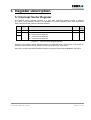
1
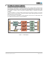
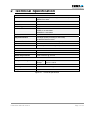
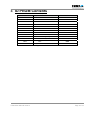
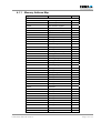
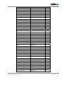
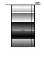
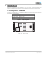
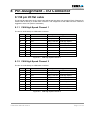
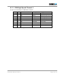
The Embedded I/O Company TIP903 3 Channel Extended CAN Bus IP Version 1.0 User Manual Issue 1.4 September 2006 D75903801 TEWS TECHNOLOGIES GmbH Am Bahnhof 7 Phone: +49-(0)4101-4058-0 25469 Halstenbek, Germany Fax: +49-(0)4101-4058-19 www.tews.com e-mail: [email protected] TEWS TECHNOLOGIES LLC 9190 Double Diamond Parkway, Suite 127, Reno, NV 89521, USA www.tews.com Phone: +1 (775) 850 5830 Fax: +1 (775) 201 0347 e-mail: [email protected] TIP903-10 3 channel extended CAN bus IndustryPack This document contains information, which is proprietary to TEWS TECHNOLOGIES GmbH. Any reproduction without written permission is forbidden. TEWS TECHNOLOGIES GmbH has made any effort to ensure that this manual is accurate and complete. However TEWS TECHNOLOGIES GmbH reserves the right to change the product described in this document at any time without notice. TEWS TECHNOLOGIES GmbH is not liable for any damage arising out of the application or use of the device described herein. Style Conventions Hexadecimal characters are specified with prefix 0x, i.e. 0x029E (that means hexadecimal value 029E). For signals on hardware products, an ‚Active Low’ is represented by the signal name with # following, i.e. IP_RESET#. Access terms are described as: W Write Only R Read Only R/W Read/Write R/C Read/Clear R/S Read/Set 1996-2006 by TEWS TECHNOLOGIES GmbH IndustryPack is a registered trademark of SBS Technologies, Inc TIP903User Manual Issue1.4 Page 2 of 18 Issue Description Date 1.0 First Issue January 1996 1.1 Programming Hints added February 1996 1.2 FPGA speed grade changed September 1997 1.3 General Revision July 2003 1.4 New address TEWS LLC September 2006 TIP903User Manual Issue1.4 Page 3 of 18 Table of Contents 1 2 3 4 PRODUCT DESCRIPTION ......................................................................................... 6 TECHNICAL SPECIFICATION................................................................................... 7 ID PROM CONTENTS ................................................................................................ 8 IP ADDRESSING........................................................................................................ 9 4.1 Memory Space Addressing............................................................................................................9 4.1.1 Memory Address Map.........................................................................................................10 5 REGISTER DESCRIPTION ...................................................................................... 14 5.1 Interrupt Vector Register..............................................................................................................14 6 PROGRAMMING HINTS .......................................................................................... 15 6.1 Programming TIP903 ....................................................................................................................15 7 INSTALLATION........................................................................................................ 16 7.1 Configuration of TIP903 ...............................................................................................................16 8 PIN ASSIGNMENT – I/O CONNECTOR .................................................................. 17 8.1 50 pin I/O flat cable .......................................................................................................................17 8.1.1 CAN High Speed Channel 1...............................................................................................17 8.1.2 CAN High Speed Channel 2...............................................................................................17 8.1.3 CAN High Speed Channel 3...............................................................................................18 TIP903User Manual Issue1.4 Page 4 of 18 Table of Figures FIGURE 1-1 : BLOCK DIAGRAM......................................................................................................................6 FIGURE 2-1 : TECHNICAL SPECIFICATION...................................................................................................7 FIGURE 3-1 : ID PROM CONTENTS ...............................................................................................................8 FIGURE 4-1 : MEMORY ADDRESS MAP ......................................................................................................13 FIGURE 5-1 : INTERRUPT VECTOR REGISTER INVTEC ...........................................................................14 FIGURE 7-1 : JUMPER CONFIGURATION....................................................................................................16 FIGURE 7-2 : JUMPER LOCATION ...............................................................................................................16 FIGURE 8-1 : CAN HIGH SPEED CHANNEL 1..............................................................................................17 FIGURE 8-2 : CAN HIGH SPEED CHANNEL 2..............................................................................................17 FIGURE 8-3 : CAN HIGH SPEED CHANNEL 3..............................................................................................18 TIP903User Manual Issue1.4 Page 5 of 18 1 Product Description The TIP903 is an IndustryPack compatible module with three complete CAN bus interfaces using three Intel 82527 CAN controllers. The controller supports the standard data and remote frame as well as the extended data and remote frame according to CAN specification 2.0 part A and part B. It has the capability to transmit, receive and perform messages filtering on extended and standard messages. The TIP903 supports a 16 bit bus interface which permits word and byte accesses to the internal registers of the three CAN controllers. The physical interface supports CAN High Speed according to ISO11898 for each of the three channels. The bus line termination is selectable by a jumper separate for each bus line. The data transfer rates up to 1Mbps for bus line length up to 40m are supported. Figure 1-1 : Block Diagram TIP903User Manual Issue1.4 Page 6 of 18 2 Technical Specification IP Interface Interface Single Size IndustryPack Logic Interface compliant to ANSI/VITA 4-1995 ID ROM Data Format I Clock Rate 8 MHz Module Type Type I Wait States IDSEL#: no wait states INTSEL#: no wait states MEMSEL#: 2 wait states CAN Controller 3 Intel 82527 CAN Controller Physical Interface CAN High Speed (according to ISO11898), 3x 82C250 CAN bus driver Bus Line Termination On board 120 ohms, selectable by jumper for each channel Number of Nodes Up to 110 on one bus line Transfer Rate Up to 1Mbps at bus line length of up to 40m I/O Interface Interface Connector 50-conductor flat cable Power Requirements 0.43A maximum @ +5V DC Physical Data Temperature Range Operating Storage 0 °C to +70 °C -25°C to +125°C MTBF 229000 h Humidity 5 – 95 % non-condensing Weight 33 g Figure 2-1 : Technical Specification TIP903User Manual Issue1.4 Page 7 of 18 3 ID PROM Contents Address Function Contents 0x01 ASCII ‘I’ 0x49 0x03 ASCII ‘P’ 0x50 0x05 ASCII ‘A’ 0x41 0x07 ASCII ‘C’ 0x43 0x09 Manufacturer ID 0xB3 0x0B Model Number 0x1C 0x0D Revision 0x10 0x0F Reserved 0x00 0x11 Driver-ID Low - Byte 0x00 0x13 Driver-ID High - Byte 0x00 0x15 Number of bytes used 0x0D 0x17 CRC 0xD4 0x19 Version -10 0x0A Figure 3-1 : ID PROM Contents TIP903User Manual Issue1.4 Page 8 of 18 4 IP Addressing 4.1 Memory Space Addressing The complete register sets of all three CAN controllers of the TIP903 and the Interrupt Vector Register INTVEC are accessible in the memory space of the IP. Byte and word accesses to the register sets of the three CAN controllers are supported. Address range: IP_memory_base_address + (0x0000 to 0x03FF) CAN controller channel 1 CANCH1: IP_memory_base_address + (0x0000 to 0x00FF) CAN controller channel 2 CANCH2: IP_memory_base_address + (0x0100 to 0x01FF) CAN controller channel 3 CANCH3: IP_memory_base_address + (0x0200 to 0x02FF) Interrupt Vector Register INTVEC: IP_memory_base_address + (0x0301) For more information about the register sets of the CAN controller refer to the data sheet of the 82527 Serial Communication Controller which is part of the TIP903-ED Engineering Documentation. TIP903User Manual Issue1.4 Page 9 of 18 4.1.1 Memory Address Map Register Offset Function Size (bit) CAN Controller Channel 1 CANCH1 0x0000 Control Register 8 0x0001 Status Register 8 0x0002 CPU Interface Register 8 0x0003 Reserved 8 0x0004 – 0x0005 High Speed Read Register 16 0x0006 – 0x0007 Global Mask – Standard 16 0x0008 – 0x000B Global Mask – Extended 16 0x000C – 0x000F Message 15 Mask 16 0x0010 – 0x001D Message 1 16 0x001E Message 1 8 0x001F CLKOUT Register 8 0x0020 – 0x002D Message 2 16 0x002E Message 2 8 0x002F Bus Configuration Register 8 0x0030 – 0x003D Message 3 16 0x003E Message 3 8 0x003F Bit Timing Register 0 8 0x0040 – 0x004D Message 4 16 0x004E Message 4 8 0x004F Bit Timing Register 1 8 0x0050 – 0x005D Message 5 16 0x005E Message 5 8 0x005F Interrupt Register 8 0x0060 – 0x006D Message 6 16 0x006E Message 6 8 0x006F Reserved 8 0x0070 – 0x007D Message 7 16 0x007E Message 7 8 0x007F Reserved 8 0x0080 – 0x008D Message 8 16 0x008E Message 8 8 0x008F Reserved 8 0x0090 – 0x009D Message 9 16 0x009E Message 9 8 0x009F P1CONF 8 0x00A0 – 0x00AD Message A 16 0x00AE Message A 8 0x00AF P2CONF 8 0x00B0 – 0x00BD Message B 16 TIP903User Manual Issue1.4 Page 10 of 18 Register Offset Function Size (bit) 0x00BE Message B 8 0x00BF P1IN 8 0x00C0 – 0x00CD Message C 16 0x00CE Message C 8 0x00CF P2IN 8 0x00D0 – 0x00DD Message D 16 0x00DE Message D 8 0x00DF P1OUT 8 0x00E0 – 0x00ED Message E 16 0x00EE Message E 8 0x00EF P2OUT 8 0x00F0 – 0x00FD Message F 16 0x00FE Message F 8 0x00FF Serial Reset Address 8 CAN Controller Channel 2 CANCH2 0x0100 Control Register 8 0x0101 Status Register 8 0x0102 CPU Interface Register 8 0x0103 Reserved 8 0x0104 – 0x0105 High Speed Read Register 16 0x0106 – 0x0107 Global Mask – Standard 16 0x0108 – 0x010B Global Mask – Extended 16 0x010C – 0x010F Message 15 Mask 16 0x0110 – 0x011D Message 1 16 0x011E Message 1 8 0x011F CLKOUT Register 8 0x0120 – 0x012D Message 2 16 0x012E Message 2 8 0x012F Bus Configuration Register 8 0x0130 – 0x013D Message 3 16 0x013E Message 3 8 0x013F Bit Timing Register 0 8 0x0140 – 0x014D Message 4 16 0x014E Message 4 8 0x014F Bit Timing Register 1 8 0x0150 – 0x015D Message 5 16 0x015E Message 5 8 0x015F Interrupt Register 8 0x0160 – 0x016D Message 6 16 0x016E Message 6 8 0x016F Reserved 8 0x0170 – 0x017D Message 7 16 TIP903User Manual Issue1.4 Page 11 of 18 Register Offset Function Size (bit) 0x017E Message 7 8 0x017F Reserved 8 0x0180 – 0x018D Message 8 16 0x018E Message 8 8 0x018F Reserved 8 0x0190 – 0x019D Message 9 16 0x019E Message 9 8 0x019F P1CONF 8 0x01A0 – 0x01AD Message A 16 0x01AE Message A 8 0x01AF P2CONF 8 0x01B0 – 0x01BD Message B 16 0x01BE Message B 8 0x01BF P1IN 8 0x01C0 – 0x01CD Message C 16 0x01CE Message C 8 0x01CF P2IN 8 0x01D0 – 0x01DD Message D 16 0x01DE Message D 8 0x01DF P1OUT 8 0x01E0 – 0x01ED Message E 16 0x01EE Message E 8 0x01EF P2OUT 8 0x01F0 – 0x01FD Message F 16 0x01FE Message F 8 Serial Reset Address 8 0x01FF CAN Controller Channel 3 CANCH3 0x0200 Control Register 8 0x0201 Status Register 8 0x0202 CPU Interface Register 8 0x0203 Reserved 8 0x0204 – 0x0205 High Speed Read Register 16 0x0206 – 0x0207 Global Mask – Standard 16 0x0208 – 0x020B Global Mask – Extended 16 0x020C – 0x020F Message 15 Mask 16 0x0210 – 0x021D Message 1 16 0x021E Message 1 8 0x021F CLKOUT Register 8 0x0220 – 0x022D Message 2 16 0x022E Message 2 8 0x022F Bus Configuration Register 8 0x0230 – 0x023D Message 3 16 TIP903User Manual Issue1.4 Page 12 of 18 Register Offset Function Size (bit) 0x023E Message 3 8 0x023F Bit Timing Register 0 8 0x0240 – 0x024D Message 4 16 0x024E Message 4 8 0x024F Bit Timing Register 1 8 0x0250 – 0x025D Message 5 16 0x025E Message 5 8 0x025F Interrupt Register 8 0x0260 – 0x026D Message 6 16 0x026E Message 6 8 0x026F Reserved 8 0x0270 – 0x027D Message 7 16 0x027E Message 7 8 0x027F Reserved 8 0x0280 – 0x028D Message 8 16 0x028E Message 8 8 0x028F Reserved 8 0x0290 – 0x029D Message 9 16 0x029E Message 9 8 0x029F P1CONF 8 0x02A0 – 0x02AD Message A 16 0x02AE Message A 8 0x02AF P2CONF 8 0x02B0 – 0x02BD Message B 16 0x02BE Message B 8 0x02BF P1IN 8 0x02C0 – 0x02CD Message C 16 0x02CE Message C 8 0x02CF P2IN 8 0x02D0 – 0x02DD Message D 16 0x02DE Message D 8 0x02DF P1OUT 8 0x02E0 – 0x02ED Message E 16 0x02EE Message E 8 0x02EF P2OUT 8 0x02F0 – 0x02FD Message F 16 0x02FE Message F 8 0x02FF Serial Reset Address 8 Interrupt Vector Register INTVEC 0x0301 Interrupt Vector Register 8 Figure 4-1 : Memory Address Map TIP903User Manual Issue1.4 Page 13 of 18 5 Register Description 5.1 Interrupt Vector Register The Interrupt Vector Register INTVEC is a byte wide read/write register located at address (IP_memory_base_address +0x0301). The INTVEC is a common register for all 3 CAN channel but each CAN channel will create an individual interrupt. Bit Description Access 7:2 Interrupt Vector loaded by software R/W 1 Interrupt from corresponding channel 00 = interrupt from channel 1 01 = interrupt from channel 2 10 = interrupt from channel 3 R/W 0 Symbol Reset Value Figure 5-1 : Interrupt Vector Register INVTEC Example: If the Interrupt Vector Register INTVEC is loaded with 0x60, CAN channel 1 will create an interrupt at vector 0x60, channel 2 at vector 0x61 and channel 3 at vector 0x62. Each of the 3 CAN channels generates interrupts on interrupt request line INTREQ0# of the IP bus. TIP903User Manual Issue1.4 Page 14 of 18 6 Programming Hints Each of the 3 CAN channel generates interrupts on interrupt request line INTREQ0# of the IP bus. The Intel 82527 CAN controller provides different interrupt sources. 6.1 Programming TIP903 It is possible that the Intel 82527 CAN controller generates an interrupt and more than one internal sources of the CAN controller request interrupt service. The TIP903 generates only one interrupt on the interrupt request line INTREQ0# of the IP. Please make sure that there is no other interrupt pending when the interrupt service will be finished. Otherwise the pending interrupt will not get an interrupt service. To make sure that there is no other pending interrupt of the CAN controller the Interrupt Register of the currently serviced CAN controller (at address location “IP_memory_base_address +0x005F, 0x015F or 0x025F”) has to be ‘0’. TIP903User Manual Issue1.4 Page 15 of 18 7 Installation Each end of a CAN bus line must be terminated by a 120 ohms resistor. If a CAN bus controller of the TIP903 is located at the end of a CAN bus line the on board bus line termination must be activated. 7.1 Configuration of TIP903 If jumper on the jumper field “J1” are installed the CAN bus line for the according CAN bus channel is terminated by a 120 ohms resistor. Jumper Bus line termination for CAN bus channel J1 (1-2) installed channel 1 active J1 (3-4) installed channel 2 active J1 (5-6) installed channel 3 active Figure 7-1 : Jumper Configuration Figure 7-2 : Jumper Location TIP903User Manual Issue1.4 Page 16 of 18 8 Pin Assignment – I/O Connector 8.1 50 pin I/O flat cable The 50 pin flat cable from the IP carrier board will be split into three 9 pin sections. Each of these 9 pin sections will fit directly to a DB9 male connector. The assignment of the DB9 connector meets the suggestion of the CiA (CAN in Automation). 8.1.1 CAN High Speed Channel 1 The line 01-09 fit directly to a DB9 male connector. I/O line DB9 Connected to TIP903 Description according to CiA 01 1 No Reserved 02 6 No (GND) Optional Input Ground 03 2 Yes CAN_L bus line CAN High Speed 04 7 Yes CAN_H bus line CAN High Speed 05 3 Yes GND Ground 06 8 No Reserved (error line) 07 4 No Reserved 08 9 No (V+) 09 5 No Reserved Optional Input Power Figure 8-1 : CAN High Speed Channel 1 8.1.2 CAN High Speed Channel 2 The line 10-18 fit directly to a DB9 male connector. I/O line DB9 Connected to TIP903 Description according to CiA 10 1 No Reserved 11 6 No (GND) Optional Input Ground 12 2 Yes CAN_L bus line CAN High Speed 13 7 Yes CAN_H bus line CAN High Speed 14 3 Yes GND Ground 15 8 No Reserved (error line) 16 4 No Reserved 17 9 No (V+) 18 5 No Reserved Optional Input Power Figure 8-2 : CAN High Speed Channel 2 TIP903User Manual Issue1.4 Page 17 of 18 8.1.3 CAN High Speed Channel 3 The line 19-27 fit directly to a DB9 male connector. I/O line DB9 Connected to TIP903 Description according to CiA 19 1 No Reserved 20 6 No (GND) Optional Input Ground 21 2 Yes CAN_L bus line CAN High Speed 22 7 Yes CAN_H bus line CAN High Speed 23 3 Yes GND Ground 24 8 No Reserved (error line) 25 4 No Reserved 26 9 No (V+) 27 5 No Reserved Optional Input Power Figure 8-3 : CAN High Speed Channel 3 TIP903User Manual Issue1.4 Page 18 of 18