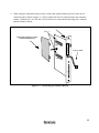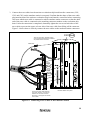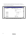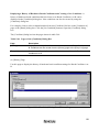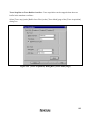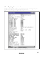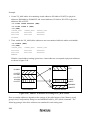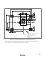
1
To our customers, Old Company Name in Catalogs and Other Documents On April 1st, 2010, NEC Electronics Corporation merged with Renesas Technology Corporation, and Renesas Electronics Corporation took over all the business of both companies. Therefore, although the old company name remains in this document, it is a valid Renesas Electronics document. We appreciate your understanding. Renesas Electronics website: http://www.renesas.com April 1st, 2010 Renesas Electronics Corporation Issued by: Renesas Electronics Corporation (http://www.renesas.com) Send any inquiries to http://www.renesas.com/inquiry. Notice 1. 2. 3. 4. 5. 6. 7. All information included in this document is current as of the date this document is issued. Such information, however, is subject to change without any prior notice. Before purchasing or using any Renesas Electronics products listed herein, please confirm the latest product information with a Renesas Electronics sales office. Also, please pay regular and careful attention to additional and different information to be disclosed by Renesas Electronics such as that disclosed through our website. Renesas Electronics does not assume any liability for infringement of patents, copyrights, or other intellectual property rights of third parties by or arising from the use of Renesas Electronics products or technical information described in this document. No license, express, implied or otherwise, is granted hereby under any patents, copyrights or other intellectual property rights of Renesas Electronics or others. You should not alter, modify, copy, or otherwise misappropriate any Renesas Electronics product, whether in whole or in part. Descriptions of circuits, software and other related information in this document are provided only to illustrate the operation of semiconductor products and application examples. You are fully responsible for the incorporation of these circuits, software, and information in the design of your equipment. Renesas Electronics assumes no responsibility for any losses incurred by you or third parties arising from the use of these circuits, software, or information. When exporting the products or technology described in this document, you should comply with the applicable export control laws and regulations and follow the procedures required by such laws and regulations. You should not use Renesas Electronics products or the technology described in this document for any purpose relating to military applications or use by the military, including but not limited to the development of weapons of mass destruction. Renesas Electronics products and technology may not be used for or incorporated into any products or systems whose manufacture, use, or sale is prohibited under any applicable domestic or foreign laws or regulations. Renesas Electronics has used reasonable care in preparing the information included in this document, but Renesas Electronics does not warrant that such information is error free. Renesas Electronics assumes no liability whatsoever for any damages incurred by you resulting from errors in or omissions from the information included herein. Renesas Electronics products are classified according to the following three quality grades: “Standard”, “High Quality”, and “Specific”. The recommended applications for each Renesas Electronics product depends on the product’s quality grade, as indicated below. You must check the quality grade of each Renesas Electronics product before using it in a particular application. You may not use any Renesas Electronics product for any application categorized as “Specific” without the prior written consent of Renesas Electronics. Further, you may not use any Renesas Electronics product for any application for which it is not intended without the prior written consent of Renesas Electronics. Renesas Electronics shall not be in any way liable for any damages or losses incurred by you or third parties arising from the use of any Renesas Electronics product for an application categorized as “Specific” or for which the product is not intended where you have failed to obtain the prior written consent of Renesas Electronics. The quality grade of each Renesas Electronics product is “Standard” unless otherwise expressly specified in a Renesas Electronics data sheets or data books, etc. “Standard”: 8. 9. 10. 11. 12. Computers; office equipment; communications equipment; test and measurement equipment; audio and visual equipment; home electronic appliances; machine tools; personal electronic equipment; and industrial robots. “High Quality”: Transportation equipment (automobiles, trains, ships, etc.); traffic control systems; anti-disaster systems; anticrime systems; safety equipment; and medical equipment not specifically designed for life support. “Specific”: Aircraft; aerospace equipment; submersible repeaters; nuclear reactor control systems; medical equipment or systems for life support (e.g. artificial life support devices or systems), surgical implantations, or healthcare intervention (e.g. excision, etc.), and any other applications or purposes that pose a direct threat to human life. You should use the Renesas Electronics products described in this document within the range specified by Renesas Electronics, especially with respect to the maximum rating, operating supply voltage range, movement power voltage range, heat radiation characteristics, installation and other product characteristics. Renesas Electronics shall have no liability for malfunctions or damages arising out of the use of Renesas Electronics products beyond such specified ranges. Although Renesas Electronics endeavors to improve the quality and reliability of its products, semiconductor products have specific characteristics such as the occurrence of failure at a certain rate and malfunctions under certain use conditions. Further, Renesas Electronics products are not subject to radiation resistance design. Please be sure to implement safety measures to guard them against the possibility of physical injury, and injury or damage caused by fire in the event of the failure of a Renesas Electronics product, such as safety design for hardware and software including but not limited to redundancy, fire control and malfunction prevention, appropriate treatment for aging degradation or any other appropriate measures. Because the evaluation of microcomputer software alone is very difficult, please evaluate the safety of the final products or system manufactured by you. Please contact a Renesas Electronics sales office for details as to environmental matters such as the environmental compatibility of each Renesas Electronics product. Please use Renesas Electronics products in compliance with all applicable laws and regulations that regulate the inclusion or use of controlled substances, including without limitation, the EU RoHS Directive. Renesas Electronics assumes no liability for damages or losses occurring as a result of your noncompliance with applicable laws and regulations. This document may not be reproduced or duplicated, in any form, in whole or in part, without prior written consent of Renesas Electronics. Please contact a Renesas Electronics sales office if you have any questions regarding the information contained in this document or Renesas Electronics products, or if you have any other inquiries. (Note 1) “Renesas Electronics” as used in this document means Renesas Electronics Corporation and also includes its majorityowned subsidiaries. (Note 2) “Renesas Electronics product(s)” means any product developed or manufactured by or for Renesas Electronics. To all our customers Regarding the change of names mentioned in the document, such as Hitachi Electric and Hitachi XX, to Renesas Technology Corp. The semiconductor operations of Mitsubishi Electric and Hitachi were transferred to Renesas Technology Corporation on April 1st 2003. These operations include microcomputer, logic, analog and discrete devices, and memory chips other than DRAMs (flash memory, SRAMs etc.) Accordingly, although Hitachi, Hitachi, Ltd., Hitachi Semiconductors, and other Hitachi brand names are mentioned in the document, these names have in fact all been changed to Renesas Technology Corp. Thank you for your understanding. Except for our corporate trademark, logo and corporate statement, no changes whatsoever have been made to the contents of the document, and these changes do not constitute any alteration to the contents of the document itself. Renesas Technology Home Page: http://www.renesas.com Renesas Technology Corp. Customer Support Dept. April 1, 2003 Cautions Keep safety first in your circuit designs! 1. Renesas Technology Corporation puts the maximum effort into making semiconductor products better and more reliable, but there is always the possibility that trouble may occur with them. Trouble with semiconductors may lead to personal injury, fire or property damage. Remember to give due consideration to safety when making your circuit designs, with appropriate measures such as (i) placement of substitutive, auxiliary circuits, (ii) use of nonflammable material or (iii) prevention against any malfunction or mishap. Notes regarding these materials 1. These materials are intended as a reference to assist our customers in the selection of the Renesas Technology Corporation product best suited to the customer's application; they do not convey any license under any intellectual property rights, or any other rights, belonging to Renesas Technology Corporation or a third party. 2. Renesas Technology Corporation assumes no responsibility for any damage, or infringement of any third-party's rights, originating in the use of any product data, diagrams, charts, programs, algorithms, or circuit application examples contained in these materials. 3. All information contained in these materials, including product data, diagrams, charts, programs and algorithms represents information on products at the time of publication of these materials, and are subject to change by Renesas Technology Corporation without notice due to product improvements or other reasons. It is therefore recommended that customers contact Renesas Technology Corporation or an authorized Renesas Technology Corporation product distributor for the latest product information before purchasing a product listed herein. The information described here may contain technical inaccuracies or typographical errors. Renesas Technology Corporation assumes no responsibility for any damage, liability, or other loss rising from these inaccuracies or errors. Please also pay attention to information published by Renesas Technology Corporation by various means, including the Renesas Technology Corporation Semiconductor home page (http://www.renesas.com). 4. When using any or all of the information contained in these materials, including product data, diagrams, charts, programs, and algorithms, please be sure to evaluate all information as a total system before making a final decision on the applicability of the information and products. Renesas Technology Corporation assumes no responsibility for any damage, liability or other loss resulting from the information contained herein. 5. Renesas Technology Corporation semiconductors are not designed or manufactured for use in a device or system that is used under circumstances in which human life is potentially at stake. Please contact Renesas Technology Corporation or an authorized Renesas Technology Corporation product distributor when considering the use of a product contained herein for any specific purposes, such as apparatus or systems for transportation, vehicular, medical, aerospace, nuclear, or undersea repeater use. 6. The prior written approval of Renesas Technology Corporation is necessary to reprint or reproduce in whole or in part these materials. 7. If these products or technologies are subject to the Japanese export control restrictions, they must be exported under a license from the Japanese government and cannot be imported into a country other than the approved destination. Any diversion or reexport contrary to the export control laws and regulations of Japan and/or the country of destination is prohibited. 8. Please contact Renesas Technology Corporation for further details on these materials or the products contained therein. User’s Manual SH7729R E8000S Emulator HS7729REBH81H User’s Manual Rev.2.0 2002.04 Cautions 1. Hitachi neither warrants nor grants licenses of any rights of Hitachi’s or any third party’s patent, copyright, trademark, or other intellectual property rights for information contained in this document. Hitachi bears no responsibility for problems that may arise with third party’s rights, including intellectual property rights, in connection with use of the information contained in this document. 2. Products and product specifications may be subject to change without notice. Confirm that you have received the latest product standards or specifications before final design, purchase or use. 3. Hitachi makes every attempt to ensure that its products are of high quality and reliability. However, contact Hitachi’s sales office before using the product in an application that demands especially high quality and reliability or where its failure or malfunction may directly threaten human life or cause risk of bodily injury, such as aerospace, aeronautics, nuclear power, combustion control, transportation, traffic, safety equipment or medical equipment for life support. 4. Design your application so that the product is used within the ranges guaranteed by Hitachi particularly for maximum rating, operating supply voltage range, heat radiation characteristics, installation conditions and other characteristics. Hitachi bears no responsibility for failure or damage when used beyond the guaranteed ranges. Even within the guaranteed ranges, consider normally foreseeable failure rates or failure modes in semiconductor devices and employ systemic measures such as fail-safes, so that the equipment incorporating Hitachi product does not cause bodily injury, fire or other consequential damage due to operation of the Hitachi product. 5. This product is not designed to be radiation resistant. 6. No one is permitted to reproduce or duplicate, in any form, the whole or part of this document without written approval from Hitachi. 7. Contact Hitachi’s sales office for any questions regarding this document or Hitachi semiconductor products. IMPORTANT INFORMATION READ FIRST • READ this user's manual before using this emulator product. • KEEP the user's manual handy for future reference. Do not attempt to use the emulator product until you fully understand its mechanism. Emulator Product: Throughout this document, the term "emulator product" shall be defined as the following products produced only by Hitachi, Ltd. excluding all subsidiary products. • • • • Emulator station Device control board Evaluation chip board Cable The user system or a host computer is not included in this definition. Purpose of the Emulator Product: This emulator product is a software and hardware development tool for systems employing the Hitachi microcomputer HD6417729R, HD6417709S, or HD6417706 (hereafter referred to as MPU). By exchanging the device control board and evaluation chip board, this emulator product can also be used for systems using other microcomputers. This emulator product must only be used for the above purpose. Limited Applications: This emulator product is not authorized for use in MEDICAL, atomic energy, aeronautical or space technology applications without consent of the appropriate officer of a Hitachi sales company. Such use includes, but is not limited to, use in life support systems. Buyers of this emulator product must notify the relevant Hitachi sales offices before planning to use the product in such applications. Improvement Policy: Hitachi, Ltd. (including its subsidiaries, hereafter collectively referred to as Hitachi) pursues a policy of continuing improvement in design, performance, and safety of the emulator product. Hitachi reserves the right to change, wholly or partially, the specifications, design, user's manual, and other documentation at any time without notice. Target User of the Emulator Product: This emulator product should only be used by those who have carefully read and thoroughly understood the information and restrictions contained in the user's manual. Do not attempt to use the emulator product until you fully understand its mechanism. It is highly recommended that first-time users be instructed by users that are well versed in the operation of the emulator product. I LIMITED WARRANTY Hitachi warrants its emulator products to be manufactured in accordance with published specifications and free from defects in material and/or workmanship. Hitachi, at its option, will repair or replace any emulator products returned intact to the factory, transportation charges prepaid, which Hitachi, upon inspection, determine to be defective in material and/or workmanship. The foregoing shall constitute the sole remedy for any breach of Hitachi's warranty. See the Hitachi warranty booklet for details on the warranty period. This warranty extends only to you, the original Purchaser. It is not transferable to anyone who subsequently purchases the emulator product from you. Hitachi is not liable for any claim made by a third party or made by you for a third party. DISCLAIMER HITACHI MAKES NO WARRANTIES, EITHER EXPRESS OR IMPLIED, ORAL OR WRITTEN, EXCEPT AS PROVIDED HEREIN, INCLUDING WITHOUT LIMITATION THEREOF, WARRANTIES AS TO MARKETABILITY, MERCHANTABILITY, FITNESS FOR ANY PARTICULAR PURPOSE OR USE, OR AGAINST INFRINGEMENT OF ANY PATENT. IN NO EVENT SHALL HITACHI BE LIABLE FOR ANY DIRECT, INCIDENTAL OR CONSEQUENTIAL DAMAGES OF ANY NATURE, OR LOSSES OR EXPENSES RESULTING FROM ANY DEFECTIVE EMULATOR PRODUCT, THE USE OF ANY EMULATOR PRODUCT, OR ITS DOCUMENTATION, EVEN IF ADVISED OF THE POSSIBILITY OF SUCH DAMAGES. EXCEPT AS EXPRESSLY STATED OTHERWISE IN THIS WARRANTY, THIS EMULATOR PRODUCT IS SOLD "AS IS ", AND YOU MUST ASSUME ALL RISK FOR THE USE AND RESULTS OBTAINED FROM THE EMULATOR PRODUCT. II State Law: Some states do not allow the exclusion or limitation of implied warranties or liability for incidental or consequential damages, so the above limitation or exclusion may not apply to you. This warranty gives you specific legal rights, and you may have other rights which may vary from state to state. The Warranty is Void in the Following Cases: Hitachi shall have no liability or legal responsibility for any problems caused by misuse, abuse, misapplication, neglect, improper handling, installation, repair or modifications of the emulator product without Hitachi's prior written consent or any problems caused by the user system. All Rights Reserved: This user's manual and emulator product are copyrighted and all rights are reserved by Hitachi. No part of this user's manual, all or part, may be reproduced or duplicated in any form, in hardcopy or machine-readable form, by any means available without Hitachi's prior written consent. Other Important Things to Keep in Mind: 1. Circuitry and other examples described herein are meant merely to indicate the characteristics and performance of Hitachi's semiconductor products. Hitachi assumes no responsibility for any intellectual property claims or other problems that may result from applications based on the examples described herein. 2. No license is granted by implication or otherwise under any patents or other rights of any third party or Hitachi. Figures: Some figures in this user's manual may show items different from your actual system. Limited Anticipation of Danger: Hitachi cannot anticipate every possible circumstance that might involve a potential hazard. The warnings in this user's manual and on the emulator product are therefore not all inclusive. Therefore, you must use the emulator product safely at your own risk. III SAFETY PAGE READ FIRST • READ this user's manual before using this emulator product. • KEEP the user's manual handy for future reference. Do not attempt to use the emulator product until you fully understand its mechanism. DEFINITION OF SIGNAL WORDS This is the safety alert symbol. It is used to alert you to potential personal injury hazards. Obey all safety messages that follow this symbol to avoid possible injury or death. DANGER WARNING CAUTION CAUTION DANGER indicates an imminently hazardous situation which, if not avoided, will result in death or serious injury. WARNING indicates a potentially hazardous situation which, if not avoided, could result in death or serious injury. CAUTION indicates a potentially hazardous situation which, if not avoided, may result in minor or moderate injury. CAUTION used without the safety alert symbol indicates a potentially hazardous situation which, if not avoided, may result in property damage. NOTE emphasizes essential information. IV WARNING Observe the precautions listed below. Failure to do so will result in a FIRE HAZARD and will damage the user system and the emulator product or will result in PERSONAL INJURY. The USER PROGRAM will be LOST. 1. Carefully handle the emulator product to prevent receiving an electric shock because the emulator product has a DC power supply. Do not repair or remodel the emulator product by yourself for electric shock prevention and quality assurance. 2. Always switch OFF the emulator and user system before connecting or disconnecting any CABLES or PARTS. 3. Always before connecting, make sure that pin 1 on both sides are correctly aligned. 4. Supply power according to the power specifications and do not apply an incorrect power voltage. Use only the provided AC power cable. Use only the specified type of fuse. V Warnings on Emulator Usage Warnings described below apply as long as you use this emulator. Be sure to read and understand the warnings below before using this emulator. Note that these are the main warnings, not the complete list. WARNING Always switch OFF the emulator and user system before connecting or disconnecting any CABLES or PARTS. Failure to do so will result in a FIRE HAZARD and will damage the user system and the emulator product or will result in PERSONAL INJURY. The USER PROGRAM will be LOST. VI CAUTION Place the emulator station and EV-chip board so that the trace cables are not bent or twisted. A bent or twisted cable will impose stress on the user interface leading to connection or contact failure. Make sure that the emulator station is placed in a secure position so that it does not move during use nor impose stress on the user interface. VII CAUTION This equipment has been tested and found to comply with the limits for a Class A digital device, pursuant to part 15 of the FCC Rules. These limits are designed to provide reasonable protection against harmful interference when the equipment is operated in a commercial environment. This equipment generates, uses, and can radiate radio frequency energy and, if not installed and used in accordance with the instruction manual, may cause harmful interference to radio communications. Operation of this equipment in a residential area is likely to cause harmful interference in which case the user will be required to correct the interference at his own expense. VIII Preface Thank you for purchasing the emulator for the Hitachi microcomputer SH7729R. CAUTION Read section 3, Preparation before Use before using the emulator product. Incorrect operation or connection will damage the user system, the emulator product, and the user program. The SH7729R E8000S emulator (hereinafter referred to as the emulator) is an efficient software and hardware development tool for systems based on Hitachi microcomputer SH7729R, SH7709S, and SH7706. By exchanging the device control board and the evaluation chip board, this emulator can also be used for systems using other microcomputers. The emulator is operated by using the Hitachi Debugging Interface (hereafter referred to as HDI). This interface program is supported by Windows 98, Windows Me, WindowsNT 4.0, and Windows 2000. This manual describes the emulator functions and operations. Please read this manual carefully before use, in particular section 1.1, Notes on Usage. A CD-R for the emulator is packaged with the evaluation chip board. For details, refer to section 3, Preparation before Use. Related Manuals: Description Notes on Using the PC Interface Board (HS6000EII01H) Description Notes on Using the PC Card Interface (HS6000EIP01H) for the E6000/E8000 Emulator Description Notes on Using the PCI Interface Board (HS6000EIC01H) for the E6000/E8000 Emulator Description Notes on Using the PCI Interface Board (HS6000EIC02H) for the E6000/E8000 Emulator Description Notes on Using the LAN Adapter (HS6000ELN01H) for the E6000/E8000 Emulator Hitachi Embedded Workshop User’s Manual SuperH RISC engine C/C++ Compiler User's Manual SuperH RISC engine Assembler User's Manual H Series Linkage Editor, Librarian, Object Converter User's Manual Hitachi Debugging Interface User's Manual i Hardware Manual supporting each MPU Programming Manual supporting each MPU Notes: 1. IBM PC is a registered trademark of International Business Machines Corporation. 2. Microsoft, Windows, and WindowsNT 4.0 are registered trademarks of Microsoft Corporation in the United States and/or in other countries. 3. PentiumIII is a registered trademark of Intel Corporation in the United States. 4. Adobe, Acrobat, and Acrobat Reader™ are registered trademarks of Adobe Systems Incorporated in the United States and/or in other countries. Abbreviation: 1.Windows 98 is an abbreviation for Microsoft Windows 98 operating system. 2.Windows Me is an abbreviation for Microsoft Windows Millenium Edition. 3.WindowsNT 4.0 is an abbreviation for Microsoft WindowsNT 4.0 operating system. 4.Windows 2000 is an abbreviation for Microsoft Windows 2000 operating system. ii Contents Section 1 Overview .............................................................................................1 1.1 1.2 1.3 Notes on Usage ................................................................................................................. 4 Environmental Conditions................................................................................................. 5 Components ...................................................................................................................... 7 1.3.1 Emulator Station .................................................................................................. 7 1.3.2 Device Control Board and Evaluation Chip Board for the SH7729R.................. 8 1.3.3 Options................................................................................................................. 9 Section 2 Components.........................................................................................11 2.1 2.2 2.3 Emulator Hardware Components ...................................................................................... 11 2.1.1 Emulator Station Components.............................................................................. 12 2.1.2 Device Control Board Components ..................................................................... 15 2.1.3 Evaluation Chip Board Configuration.................................................................. 16 Configuration of the Provided CD-R ................................................................................ 18 System Configuration........................................................................................................20 2.3.1 System Configuration Using a PC Interface Board .............................................. 20 Section 3 Preparation before Use ........................................................................23 3.1 3.2 3.3 3.4 3.5 3.6 3.7 Description on Emulator Usage ........................................................................................ 23 Installing the Acrobat® Reader™...................................................................................... 24 Emulator Connection......................................................................................................... 24 3.3.1 Connecting the Device Control Board ................................................................. 24 3.3.2 Connecting the Evaluation Chip Board................................................................ 27 3.3.3 Connecting the External Probe............................................................................. 32 3.3.4 Selecting the Clock .............................................................................................. 33 3.3.5 Connecting the System Ground............................................................................ 35 3.3.6 System Connection............................................................................................... 37 Setting Up with Windows® Operating Systems................................................................. 38 3.4.1 Setting Up the PCI Interface Board on Windows® 98 or Windows® Me............. 38 3.4.2 Setting Up the PC Interface Board on Windows NT® 4.0 ................................... 39 3.4.3 Setting Up the PC Interface Board on Windows® 2000....................................... 41 3.4.4 PC Interface Board Specifications (ISA Bus Specifications)............................... 42 Installing the System Program........................................................................................... 50 Initiating the HDI and Checking the Emulator.................................................................. 57 Troubleshooting ................................................................................................................ 60 3.7.1 Error Messages from the HDI .............................................................................. 60 iii 3.8 3.7.2 Error Messages from the Emulator ...................................................................... 62 3.7.3 Troubleshooting Procedure .................................................................................. 65 3.7.4 Operating Procedure for the Diagnostic Program ................................................ 67 Uninstallation .................................................................................................................... 69 3.8.1 Uninstalling Software........................................................................................... 69 3.8.2 Uninstalling the Acrobat® Reader™ .................................................................... 69 Section 4 Tutorial................................................................................................71 4.1 4.2 4.3 4.4 4.5 4.6 4.7 4.8 4.9 4.10 4.11 4.12 4.13 Introduction....................................................................................................................... 71 Running the HDI ............................................................................................................... 72 Setting the Configuration .................................................................................................. 75 Setting the Memory Map................................................................................................... 77 Downloading ..................................................................................................................... 80 4.5.1 Downloading the Sample Program....................................................................... 80 4.5.2 Displaying the Source Program............................................................................ 81 Setting the Software Breakpoints ...................................................................................... 83 Executing the Program ...................................................................................................... 84 Reviewing Breakpoints ..................................................................................................... 86 Viewing Memory .............................................................................................................. 87 Watching Variables........................................................................................................... 89 Stepping Through a Program ............................................................................................ 92 4.11.1 Executing [Step In] Command ............................................................................. 94 4.11.2 Executing [Step Out] Command .......................................................................... 95 4.11.3 Executing [Step Over] Command ........................................................................ 98 Displaying Local Variables ............................................................................................... 10 0 Saving and Loading the Session........................................................................................ 102 Section 5 Emulator Functions.............................................................................103 5.1 5.2 5.3 5.4 5.5 iv Introduction....................................................................................................................... 103 Setting the Emulator’s Operating Conditions.................................................................... 104 5.2.1 Configuration Dialog Box.................................................................................... 106 5.2.2 [CPU Operating Mode] Dialog Box .................................................................... 119 Realtime Emulation........................................................................................................... 129 5.3.1 Execution ............................................................................................................. 129 5.3.2 Trace-Halt Mode.................................................................................................. 132 5.3.3 Display of Cause for Termination and Operating Status...................................... 133 Step Functions................................................................................................................... 135 5.4.1 Step Execution ..................................................................................................... 135 5.4.2 Interrupts during Step Execution.......................................................................... 136 Break Functions ................................................................................................................ 136 5.6 5.7 5.8 5.9 5.10 5.11 5.12 5.13 5.14 5.15 5.16 5.5.1 Software Break..................................................................................................... 138 5.5.2 Software Sequential Break ................................................................................... 142 5.5.3 Hardware Break ................................................................................................... 148 5.5.4 Hardware Sequential Break.................................................................................. 164 5.5.5 Internal Break....................................................................................................... 171 5.5.6 Internal Sequential Break..................................................................................... 181 5.5.7 Forced Break........................................................................................................ 182 5.5.8 Forced Break on Writing to a Write-Protected Area............................................ 182 5.5.9 Break Due to Trace-Buffer Overflow .................................................................. 182 5.5.10 Timeout Break ..................................................................................................... 183 Trace Functions................................................................................................................. 184 5.6.1 External Bus Trace Function................................................................................ 184 5.6.2 External Bus Trace Timing .................................................................................. 198 5.6.3 AUD Trace Function............................................................................................ 201 5.6.4 Trace Display....................................................................................................... 203 5.6.5 Trace Search Functions........................................................................................ 208 Measurement of Execution Time ...................................................................................... 216 5.7.1 Measuring Execution Time to a Break or Termination........................................ 216 5.7.2 Measuring Execution Time between Satisfaction of Specified Conditions.......... 217 Performance Analysis Function......................................................................................... 219 5.8.1 Measuring with Emulator Station Function.......................................................... 219 Displaying Various Information........................................................................................ 237 Trigger Output................................................................................................................... 240 Memory Spaces and VP_MAP Translation ...................................................................... 241 5.11.1 The Allocation of Emulation Memory ................................................................. 241 5.11.2 VP_MAP Translation........................................................................................... 243 5.11.3 Programs which use the MMU............................................................................. 247 5.11.4 Notes on Accessing Memory ............................................................................... 247 Stack Trace Function......................................................................................................... 249 Auto-Update Memory Function ........................................................................................ 251 5.13.1 Overview.............................................................................................................. 251 5.13.2 Setting Auto update Memory ............................................................................... 252 5.13.3 Displaying the Memory........................................................................................ 253 Controlling and Checking the State of the MPU ............................................................... 256 5.14.1 Selecting Clock for the MPU ............................................................................... 256 5.14.2 Checking the I/O Signals...................................................................................... 256 5.14.3 Checking the Power Supply and Clock State of the User System ........................ 257 Input Format...................................................................................................................... 258 5.15.1 Entering Masks .................................................................................................... 258 [Source] Window Expanded Function .............................................................................. 259 v 5.16.1 Setting BP Column............................................................................................... 259 Section 6 6.1 6.2 Command Line ................................................................................261 List Format........................................................................................................................ 261 6.1.1 Description........................................................................................................... 261 6.1.2 Format.................................................................................................................. 261 6.1.3 Parameter Type Input........................................................................................... 262 6.1.4 Examples.............................................................................................................. 262 List of Commands ............................................................................................................. 262 6.2.1 Hardware Break Command (BCS, BCC, BCD, BCE) ......................................... 267 6.2.2 Internal Break Commands (BCUS, BCUC, BCUD, BCUE) ............................... 273 6.2.3 Hardware Sequential Break Specification Command (CSQ) ............................... 278 6.2.4 Software Break Command (BP, BC, BD, BE)..................................................... 280 6.2.5 Software Sequential Break Command (BSS, BSC, BSD, BSE) .......................... 284 6.2.6 CHECK (CHECK)............................................................................................... 288 6.2.7 CLOCK (CK)....................................................................................................... 290 6.2.8 DEVICE_TYPE (DE).......................................................................................... 292 6.2.9 END (END) ......................................................................................................... 293 6.2.10 EXECUTION_MODE (EM) ............................................................................... 294 6.2.11 GO_OPTION (GP) .............................................................................................. 297 6.2.12 ID (ID) ................................................................................................................. 299 6.2.13 MAP_SET (MS) .................................................................................................. 300 6.2.14 MEMORYAREA_SET (MAS)............................................................................ 301 6.2.15 Performance Command (PS, PC, PA).................................................................. 303 6.2.16 REFRESH (RF) ................................................................................................... 310 6.2.17 STATUS (STS).................................................................................................... 311 6.2.18 Trace Condition Command (TAS, TAC, TAD)................................................... 313 6.2.19 TRACE_DISPLAY (TD)..................................................................................... 320 6.2.20 TRACE_MODE (TM) ......................................................................................... 321 6.2.21 TRACE_SEARCH (TS) ...................................................................................... 323 6.2.22 Address Translation Table Command (VS, VC, VD, VE)................................... 327 Section 7 Error Messages....................................................................................331 7.1 7.2 7.3 Emulator Error Messages.................................................................................................. 331 HDI Error Messages Related to the Emulator................................................................... 334 Error Messages for the LAN Driver.................................................................................. 337 Appendix A User System Interface ...................................................................339 A.1 vi User System Interface Circuit ........................................................................................... 339 Appendix B Preparations for Assembling the User System Board....................349 B.1 B.2 Recommended Dimensions for the User System Connector (HS7729REBH81H) ........... 349 Recommended Dimensions for the User System Connector (HS7706EBH81H).............. 352 Appendix C Connecting the Emulator to the User System................................355 C.1 C.2 C.3 Connecting the Evaluation Chip Board to the User System .............................................. 355 Connecting the Cables for Tracing.................................................................................... 359 Installing the MPU on the User System ............................................................................ 362 Appendix D SH7729R Internal Module Support...............................................365 D.1 D.2 D.3 D.4 D.5 D.6 Memory Space .................................................................................................................. 365 D.1.1 Internal I/O Area .................................................................................................. 365 D.1.2 External Memory Area......................................................................................... 365 Low Power-consumption Mode (Sleep, Software Standby, and Hardware Standby) ..... 366 D.2.1 Sleep and Software Standby Modes..................................................................... 366 Interrupts ........................................................................................................................... 366 Control Input Signals (RESETP, RESETM, BREQ, and WAIT) ..................................... 366 Bus State Controller .......................................................................................................... 367 Emulator Status and Internal Modules .............................................................................. 367 Appendix E Notes on Debugging ......................................................................369 E.1 E.2 E.3 E.4 E.5 E.6 E.7 E.8 E.9 The Tracing Function........................................................................................................369 Emulation Memory ........................................................................................................... 369 User Interface.................................................................................................................... 370 Performance Measurement Function................................................................................. 371 Hardware Break Function ................................................................................................. 371 Hardware Sequential Break/Trace Function ..................................................................... 371 Clock Operating Mode...................................................................................................... 371 Differences between the Emulator and the SH7729R ....................................................... 372 Step Function .................................................................................................................... 374 vii Figures Figure 1.1 Emulator for the SH7729R (Connected via the IC Socket) ...........................................2 Figure 2.1 Emulator Hardware Components.................................................................................11 Figure 2.2 Emulator Station: Front Panel ..................................................................................... 12 Figure 2.3 Emulator Station: Rear Panel....................................................................................... 13 Figure 2.4 Device Control Board..................................................................................................15 Figure 2.5 Evaluation Chip Board (HS7729REBH81H) .............................................................. 16 Figure 2.6 System Configuration Using a PC Interface Board ..................................................... 20 Figure 2.7 System Configuration Using a LAN Adapter .............................................................. 21 Figure 3.1 Emulator Preparation Flowchart.................................................................................. 23 Figure 3.2 Connecting the Memory Board.................................................................................... 25 Figure 3.3 Connecting the Device Control Board......................................................................... 26 Figure 3.4 Connecting Trace Cables to the Emulator Station ....................................................... 29 Figure 3.5 Connecting Trace Cables to the Evaluation Chip Board ............................................. 31 Figure 3.6 External Probe Connector............................................................................................32 Figure 3.7 Installing the Crystal Oscillator ...................................................................................34 Figure 3.8 Connecting the System Ground ................................................................................... 35 Figure 3.9 Connecting the Frame Ground..................................................................................... 36 Figure 3.10 Host Interface Switches .............................................................................................37 Figure 3.11 Allocatable Memory Area of PC Interface Board ..................................................... 43 Figure 3.12 PC Interface Board Switch ........................................................................................44 Figure 3.13 Installing the PC Interface Board .............................................................................. 45 Figure 3.14 Connecting the Emulator Station to the PC Interface Board .....................................46 Figure 3.15 [Start] Menu (System Install Tool) ............................................................................ 52 Figure 3.16 [Browse for Folder] Dialog Box................................................................................ 53 Figure 3.17 [E8000 Load Files] Dialog Box................................................................................. 54 Figure 3.18 [System Install Completed!!] Dialog Box..................................................................55 Figure 3.19 [E8000 Load Files] Dialog Box................................................................................. 56 Figure 3.20 [Start] Menu (Initiating the HDI)............................................................................... 57 Figure 3.21 [Select Session] Dialog Box ......................................................................................58 Figure 3.22 [Driver Details] Dialog Box (When ISA Bus Is Selected) ........................................ 58 Figure 3.23 Status Bar during the HDI Initiation.......................................................................... 59 Figure 3.24 Status Bar at the HDI Initiation Completion.............................................................. 59 Figure 3.25 CPU Operating Mode Modification Message Mode (1)............................................ 59 Figure 3.26 CPU Operating Mode Modification Message Mode (2)............................................ 60 Figure 3.27 Error Message on PC Interface Board Connection Failure........................................ 60 Figure 3.28 Error Message on Emulator Connection Failure........................................................ 61 Figure 3.29 Troubleshooting PAD................................................................................................66 Figure 3.30 Diagnostic Program Initiation Confirmation Dialog Box .......................................... 67 viii Figure 3.31 [DIAGNOSTIC PROGRAM] Dialog Box ................................................................ 67 Figure 3.32 Terminating the Diagnostic Program (by Clicking the STOP Button) ...................... 68 Figure 4.1 [Start] Menu ................................................................................................................72 Figure 4.2 HDI Window ...............................................................................................................74 Figure 4.3 [Configuration] Dialog Box......................................................................................... 75 Figure 4.4 [Memory Mapping] Dialog Box (before Setting) ........................................................ 77 Figure 4.5 [Add Memory Mapping] Dialog Box .......................................................................... 78 Figure 4.6 [Memory Mapping] Dialog Box (at Setting) ............................................................... 79 Figure 4.7 [Load Program] Dialog Box ........................................................................................ 80 Figure 4.8 HDI Dialog Box ..........................................................................................................80 Figure 4.9 [Open] Dialog Box ......................................................................................................81 Figure 4.10 [Source] Window (Displaying the Source Program) ................................................. 82 Figure 4.11 [Source] Window (Setting a Software Breakpoint) ................................................... 83 Figure 4.12 [Source] Window (Break State)................................................................................. 84 Figure 4.13 [System Status] Window ...........................................................................................85 Figure 4.14 [Breakpoints] Window .............................................................................................. 86 Figure 4.15 [Open Memory Window] Dialog Box ....................................................................... 87 Figure 4.16 [Long Memory] Window........................................................................................... 88 Figure 4.17 [Instant Watch] Dialog Box.......................................................................................89 Figure 4.18 [Watch Window] Window (Displaying the Array).................................................... 90 Figure 4.19 [Add Watch] Dialog Box........................................................................................... 90 Figure 4.20 [Watch Window] Window (Displaying the Variable) ............................................... 91 Figure 4.21 [Watch Window] Window (Displaying Array Elements) .......................................... 91 Figure 4.22 [Source] Window (Step Execution)........................................................................... 93 Figure 4.23 [Source] Window (Step In)........................................................................................94 Figure 4.24 [Source] Window (Step Out) ..................................................................................... 95 Figure 4.25 [Watch Window] Display Example (1) .....................................................................96 Figure 4.26 [Source] Window (Step Out → Step In)....................................................................96 Figure 4.27 [Watch Window] Display Example (2) .....................................................................97 Figure 4.28 [Source] Window (Before Step Over Execution) ...................................................... 98 Figure 4.29 [Source] Window (Step Over) ................................................................................... 99 Figure 4.30 [Watch Window] Display Example (3) .....................................................................99 Figure 4.31 [Locals] Window .....................................................................................................100 Figure 4.32 [Locals] Window (Displaying Array a Elements) ................................................... 101 Figure 5.1 [Configuration] Dialog Box....................................................................................... 106 Figure 5.2 [Configuration] Dialog Box ([General] Page) ........................................................... 107 Figure 5.3 [Configuration] Dialog Box ([Execution Mode1] Page) ........................................... 110 Figure 5.4 [Configuration] Dialog Box ([Execution Mode2] Page) ........................................... 112 Figure 5.5 [Configuration] Dialog Box ([Loading flash memory] Page)....................................114 Figure 5.6 [Configuration] Dialog Box ([CPU Operating Mode] Page).....................................118 ix Figure 5.7 [CPU Operating Mode] Dialog Box ([Device] Page)................................................ 120 Figure 5.8 [CPU Operating Mode] Dialog Box ([MD Pin] Page) .............................................. 121 Figure 5.9 [CPU Operating Mode] Dialog Box ([Memory Type] Page) ....................................124 Figure 5.10 [CPU Operating Mode] Dialog Box ([I/O Port] Page (SH7729R/SH7709S)) ........126 Figure 5.11 [CPU Operating Mode] Dialog Box ([H-UDI (JTAG) Clock] Page) ...................... 128 Figure 5.12 Timing for Trigger Signal Output............................................................................ 131 Figure 5.13 [Breakpoints] Window ............................................................................................ 136 Figure 5.14 Example of a Software Break Instruction ................................................................ 138 Figure 5.15 [Point] Page ([Break] Dialog Box).......................................................................... 139 Figure 5.16 [Break Point] Dialog Box ([Address] Page) ............................................................ 140 Figure 5.17 Example of a Software Sequential Break ................................................................ 142 Figure 5.18 Example of a Software Sequential Break (Reset Point Specification)..................... 143 Figure 5.19 [Break] Dialog Box ([Sequence] Page) ...................................................................144 Figure 5.20 [Break Sequence] Dialog Box ................................................................................. 145 Figure 5.21 Example of a Hardware Break with a Satisfaction-Count Condition Specified....... 148 Figure 5.22 Example of a Hardware Break with Delay Condition Specified.............................. 149 Figure 5.23 [Break] Dialog Box ([Condition A] Page)............................................................... 150 Figure 5.24 [Break Condition A7] Dialog Box ([Address] Page)............................................... 152 Figure 5.25 [Break Condition A7] Dialog Box ([Data] Page) .................................................... 154 Figure 5.26 [Break Condition A7] Dialog Box ([Bus State] Page)............................................. 155 Figure 5.27 [Break Condition A7] Dialog Box ([Probe] Page) .................................................. 156 Figure 5.28 [Break Condition A7] Dialog Box ([Interrupt] Page).............................................. 157 Figure 5.29 [Break Condition A7] Dialog Box ([Count] Page) .................................................. 159 Figure 5.30 [Break Condition A7] Dialog Box ([Delay] Page) .................................................. 160 Figure 5.31 [Condition] Dialog Box ([History] Page) ................................................................ 161 Figure 5.32 [Condition] Dialog Box ([Entry List] Page) ............................................................ 162 Figure 5.33 [Configuration] Dialog Box (Hardware Sequential Break) .....................................164 Figure 5.34 [Break] Dialog Box (after Setting a Hardware Sequential Break)........................... 165 Figure 5.35 [Condition] Dialog Box ([History] Page) ................................................................ 167 Figure 5.36 [Condition] Dialog Box ([Entry List] Page) ............................................................ 169 Figure 5.37 Example: Display of the Status of a Hardware Sequential Break Condition ........... 170 Figure 5.38 [Break] Dialog Box ([Condition U] Page)............................................................... 172 Figure 5.39 [Break Condition U1] Dialog Box ([Address] Page)............................................... 174 Figure 5.40 [Break Condition U1] Dialog Box ([Data] Page) .................................................... 176 Figure 5.41 [Break Condition U1] Dialog Box ([ASID] Page) .................................................. 177 Figure 5.42 [Break Condition U1] Dialog Box ([Bus State] Page)............................................. 178 Figure 5.43 [Break Condition U1] Dialog Box ([Count] Page) .................................................. 179 Figure 5.44 [Break Condition U3] Dialog Box........................................................................... 180 Figure 5.45 [Break Condition U4] Dialog Box........................................................................... 180 Figure 5.46 [Configuration] Dialog Box (Internal Sequential Break)......................................... 181 x Figure 5.47 Figure 5.48 Figure 5.49 Figure 5.50 Figure 5.51 Figure 5.52 Figure 5.53 Figure 5.54 Figure 5.55 Figure 5.56 Figure 5.57 Figure 5.58 Figure 5.59 Figure 5.60 Figure 5.61 Figure 5.62 Figure 5.63 Figure 5.64 Figure 5.65 Figure 5.66 Figure 5.67 Figure 5.68 Figure 5.69 Figure 5.70 Figure 5.71 Figure 5.72 Figure 5.73 Figure 5.74 Figure 5.75 Figure 5.76 Figure 5.77 Figure 5.78 Figure 5.79 Figure 5.80 Figure 5.81 Figure 5.82 Figure 5.83 Figure 5.84 Figure 5.85 Figure 5.86 [Trace Acquisition] Dialog Box (Trace Buffer Overflow) ...................................... 182 [Configuration] Dialog Box (Timeout Break) ......................................................... 183 Trace Acquisition in Free Trace Mode....................................................................185 Trace Acquisition in Trace-Stop Mode ...................................................................186 [Trace Acquisition] Dialog Box ([Condition A] Page)............................................ 188 [Trace Condition A7] Dialog Box ([General] Page) ............................................... 189 [Configuration] Dialog Box (Sequential Trace Stop) .............................................. 192 [Trace Acquisition] Dialog Box ([Trace Mode] Page)............................................ 193 Example of Range Trace Mode ............................................................................... 194 [Configuration] Dialog Box ([General] Page) ......................................................... 196 [Trace Acquisition] Page ([Bus Trace] Group Box)................................................ 197 Bus Trace for Normal SRAM.................................................................................. 199 Bus Trace for SDRAM ............................................................................................ 200 [Trace Acquisition] Dialog Box ([Trace Mode] Page)............................................ 201 [Trace Filter] Dialog Box ([General] Page)............................................................. 203 [Trace] Window ......................................................................................................204 [Trace] Window (AUD Trace Display) ...................................................................206 [Trace] Window (Mixed Display of External Bus Trace and AUD Trace) ............. 208 [Trace Filter] Dialog Box ([General] Page)............................................................. 209 [Trace Filter] Dialog Box ([Time] Page).................................................................213 [Trace Filter] Dialog Box ([AUD] Page).................................................................214 [Trace Find] Dialog Box ([General] Page).............................................................. 215 [System Status] Window (Display of Execution Time) ........................................... 216 [Performance Analysis] Window............................................................................. 219 Example of Subroutine Time Measurement Mode 1 ............................................... 221 Example of Subroutine Time Measurement Mode 2 ............................................... 222 Example of Subroutine Time Measurement Mode 3 ............................................... 223 [Performance Analysis] Dialog Box........................................................................ 225 [Performance 1] Dialog Box ([General] Page) ........................................................ 227 [Performance 1] Dialog Box ([Address] Page)........................................................ 228 [Performance 1] Dialog Box ([Address] Page)........................................................ 229 [Performance 1] Dialog Box ([Time Out] Page) ..................................................... 231 [Performance 1] Dialog Box ([Count] Page) ........................................................... 232 [Input Function Range] Dialog Box ........................................................................ 233 [Performance Analysis] Window (Measurement of Executed Addresses) .............. 234 [Performance Analysis] Window (Run Time and Execution Count)....................... 235 [Performance Analysis] Window (Execution Time Ratios).....................................236 [System Status] Window ......................................................................................... 237 Pulse Output Timing................................................................................................240 [Memory Mapping] Dialog Box .............................................................................. 241 xi Figure 5.87 [Edit Memory Mapping] Dialog Box ...................................................................... 242 Figure 5.88 Address Translation According to VP_MAP Tables............................................... 244 Figure 5.89 [Stack Trace] Window.............................................................................................249 Figure 5.90 [Stack Trace Setting] Dialog Box............................................................................ 250 Figure 5.91 [AUM] Window ......................................................................................................251 Figure 5.92 [AUM – Target Details] Dialog Box ....................................................................... 253 Figure 5.93 [Auto-update Memory -Edit-] Dialog Box .............................................................. 254 Figure 6.1 Address Translation...................................................................................................328 Figure A.1 Basic Bus Cycle........................................................................................................ 340 Figure A.2 User System Interface Circuits (1) ........................................................................... 341 Figure A.2 User System Interface Circuits (2) ........................................................................... 342 Figure A.2 User System Interface Circuits (3) ........................................................................... 343 Figure A.2 User System Interface Circuits (4) ........................................................................... 344 Figure A.2 User System Interface Circuits (5) ........................................................................... 345 Figure A.2 User System Interface Circuits (6) ........................................................................... 346 Figure A.2 User System Interface Circuits (7) ........................................................................... 347 Figure B.1 Recommended Dimensions for Mount Pad (Top View) ........................................... 350 Figure B.2 Restrictions on Parts Location .................................................................................. 351 Figure B.3 Recommended Dimensions for Mount Pad (Top View) ........................................... 353 Figure B.4 Restrictions on Parts Location .................................................................................. 354 Figure C.1 Installing the IC Socket.............................................................................................355 Figure C.2 Order of Tightening the Screws (Top View of the HS7729REBH81H Board) ........357 Figure C.3 Connecting the HS7729REBH81H Board to the User System .................................358 Figure C.4 Connecting the Trace Cables to the Evaluation Chip Board ..................................... 361 Figure C.5 Installing the MPU....................................................................................................363 xii Tables Table 1.1 Environmental Conditions ......................................................................................... 5 Table 1.2 Operating Environment.............................................................................................. 6 Table 1.3 Emulator Station Components (HS8000EST11H)..................................................... 7 Table 1.4 Device Control Board Components ........................................................................... 8 Table 1.5 Evaluation Chip Board Components for the SH7729R ............................................. 8 Table 1.6 Evaluation Chip Board Components for the SH7706 ................................................ 9 Table 1.7 Optional Component Specifications .......................................................................... 9 Table 2.1 Contents of CD-R ...................................................................................................... 18 Table 3.1 PC Interface Board Specifications ............................................................................. 42 Table 3.2 Switch Settings for Memory Areas ............................................................................ 44 Table 3.3 Contents of Emulator System Programs for the SH7729R and SH7709S ................. 50 Table 3.4 Contents of Emulator System Programs for the SH7706 ........................................... 51 Table 3.5 Types of Connection and Drivers .............................................................................. 52 Table 3.6 [DIAGNOSTIC PROGRAM] Dialog Box ................................................................ 68 Table 4.1 Configuration of the Sample Program ....................................................................... 71 Table 4.2 [CPU Operation Mode] Dialog Box Setting Example ............................................... 73 Table 4.3 Settings in the [Configuration] Dialog Box ............................................................... 76 Table 4.4 Step Command........................................................................................................... 92 Table 5.1 Emulator Functions.................................................................................................... 103 Table 5.2 Setting the Emulator’s Operating Conditions ............................................................ 104 Table 5.3 [Configuration] Dialog Box....................................................................................... 106 Table 5.4 [General] Page ........................................................................................................... 108 Table 5.5 [Execution Mode1] Page ........................................................................................... 111 Table 5.6 [Execution Mode2] Page ........................................................................................... 113 Table 5.7 [Loading flash memory] Page.................................................................................... 115 Table 5.8 Module Interface........................................................................................................ 116 Table 5.9 Sample Program Specifications ................................................................................. 117 Table 5.10 [CPU Operating Mode] Page................................................................................... 118 Table 5.11 [CPU Operating Mode] Dialog Box ........................................................................ 119 Table 5.12 [Device] Page .......................................................................................................... 120 Table 5.13 [MD Pin] Page ......................................................................................................... 122 Table 5.14 Cases Different from the [CPU Operating Mode] Settings...................................... 123 Table 5.15 [Memory Type] Page ............................................................................................... 125 Table 5.16 [I/O Port] Page......................................................................................................... 127 Table 5.17 [H-UDI (JTAG) Clock] Page................................................................................... 128 Table 5.18 Realtime Execution.................................................................................................. 129 Table 5.19 Emulation Modes..................................................................................................... 130 Table 5.20 Restrictions on Emulation Modes ............................................................................ 131 xiii Table 5.21 Table 5.22 Table 5.23 Table 5.24 Table 5.25 Table 5.26 Table 5.27 Table 5.28 Table 5.29 Table 5.30 Table 5.31 Table 5.32 Table 5.33 Table 5.34 Table 5.35 Table 5.36 Table 5.37 Table 5.38 Table 5.39 Table 5.40 Table 5.41 Table 5.42 Table 5.43 Table 5.44 Table 5.45 Table 5.46 Table 5.47 Table 5.48 Table 5.49 Table 5.50 Table 5.51 Table 5.52 Table 5.53 Table 5.54 Table 5.55 Table 5.56 Table 5.57 Table 5.58 Table 5.59 xiv Causes for Termination............................................................................................ 133 Operating Status Display ......................................................................................... 134 Step Execution ......................................................................................................... 135 Break Functions ....................................................................................................... 137 [Point] Page Options................................................................................................ 139 [Break Point] Dialog Box Options........................................................................... 140 [Sequence] Page Options ......................................................................................... 144 [Break Sequence] Page Options .............................................................................. 146 Hardware Break Conditions..................................................................................... 148 Specifiable Hardware Break Conditions.................................................................. 149 [Condition A, B, C] Page Options ........................................................................... 151 [Break Condition A1 to A8, B1 to B8, C1 to C8] Dialog Box Pages ...................... 151 [Address] Page Options ........................................................................................... 153 [Data] Page Options................................................................................................. 154 [Bus State] Page Options ......................................................................................... 155 [Probe] Page Options............................................................................................... 156 [Interrupt] Page Options .......................................................................................... 157 [Count] Page Options .............................................................................................. 159 [Delay] Page Options............................................................................................... 160 Pages of the [Condition] Dialog Box....................................................................... 161 [History] Page Options ............................................................................................ 162 [Entry List] Page Options ........................................................................................ 163 [Condition A/B] Page Options (When a Hardware Sequential Break Has Been Specified) ..................................... 165 [History] Page Options ............................................................................................ 168 [Entry List] Page Options ........................................................................................ 170 Internal Break Conditions........................................................................................ 171 Specifiable Internal Break Conditions ..................................................................... 172 [Condition U] Page Options .................................................................................... 173 [Break Condition U1 – U4] Dialog Box Pages........................................................ 173 [Address] Page Options ........................................................................................... 174 [Data] Page Options................................................................................................. 176 [ASID] Page Options............................................................................................... 177 [Bus State] Group Box............................................................................................. 178 [Read/Write] Group Box ......................................................................................... 178 [Count] Page Options .............................................................................................. 179 [Break Condition U3, U4] Page Options ................................................................. 180 Internal Sequential Break Modes (Break Condition U1 and U2) ............................ 181 Trace Acquisition Modes......................................................................................... 185 Trace Stop Conditions .............................................................................................187 Table 5.60 Table 5.61 Table 5.62 Table 5.63 Table 5.64 Table 5.65 Table 5.66 Table 5.67 Table 5.68 Table 5.69 Table 5.70 Table 5.71 Table 5.72 Table 5.73 Table 5.74 Table 5.75 Table 5.76 Table 5.77 Table 5.78 Table 5.79 Table 5.80 Table 5.81 Table 5.82 Table 5.83 Table 5.84 Table 5.85 Table 5.86 Table 5.87 Table 5.88 Table 5.89 Table 5.90 Table 5.91 Table 5.92 Table 5.93 Table 5.94 Table 5.95 Table 5.96 Table 5.97 Specifiable Trace-Stop Conditions .......................................................................... 187 [Condition A, B, C] Page Options ........................................................................... 189 [Trace Condition A1 to A8, B1 to B8, C1 to C8] Dialog Box Pages ...................... 190 Pages of the [Condition] Dialog Box Pages............................................................. 191 Range Trace Conditions........................................................................................... 194 Specifiable Range Trace Conditions........................................................................ 195 [Trace Condition A1 to A8, B1 to B8, C1 to C8] Dialog Box Pages ...................... 195 [Bus Trace] Group Box Options.............................................................................. 198 AUD Trace Acquisition Mode................................................................................. 201 [AUD Trace] Group Box ......................................................................................... 202 External Bus Trace Information Items and Display Format in [Trace] Window ..... 205 AUD Trace Information Items and Display Format in [Trace] Window ................. 207 Trace Search Functions............................................................................................208 [General] Page Options............................................................................................ 210 Trace Search Conditions and Pages in the [Trace Filter] Dialog Box ..................... 211 [Time] Page Options............................................................................................... . 213 [AUD] Page Options................................................................................................ 214 Measurement Modes................................................................................................ 220 Modes that are Available in the [Performance1 to 8] Dialog Boxes........................ 223 Pages of the [Performance 1 to 8] Dialog Box ........................................................ 226 Options on the [General] page ................................................................................. 227 Options on the [Address] page (When [Subroutine time measurement mode 1,2] is Selected) ................................ 228 Options on the [Address] Page (When [Subroutine time measurement mode 3] is Selected) ................................... 230 Options of the [Time Out] Page............................................................................... 231 Options on the [Count] Page.................................................................................... 232 Menu Items for Displaying the Results.................................................................... 233 Display Format of Results When [Address] is Selected .......................................... 234 Display Format of Results When [Count] is Selected.............................................. 235 Display Format of Results When [Graph] is Selected ............................................. 236 [System Status] Window Configuration................................................................... 238 [Session] Sheet Configuration ................................................................................. 238 [Platform] Sheet Configuration................................................................................ 239 [Memory] Sheet Configuration ................................................................................ 239 [Events] Sheet Configuration................................................................................... 240 Configuration Items of the [Memory Mapping] Dialog Box ................................... 242 Configuration Items of the [Edit Memory Mapping] Dialog Box............................ 243 Settings for Memory Type Available in the [Setting] Combo Box.......................... 243 Address Translation Tables ..................................................................................... 246 xv Table 5.98 Settings for Memory Type Available in the [Setting] Combo Box.......................... 247 Table 5.99 [Stack Trace] Window Options ............................................................................... 249 Table 5.100 Options in the Pop-up Menu .................................................................................. 249 Table 5.101 [Stack Trace Setting] Dialog Box Options ............................................................ 250 Table 5.102 Dialog Boxes for Setting Auto-Update Memory Items.......................................... 251 Table 5.103 Address Mask Specification .................................................................................. 258 Table 5.104 BP Column Display Item ....................................................................................... 259 Table 6.1 List of Commands...................................................................................................... 263 Table 7.1 Error Messages .......................................................................................................... 332 Table 7.2 HDI Error Messages .................................................................................................. 334 Table A.1 Bus Timing when Using the Emulator...................................................................... 339 Table D.1 Emulator State and Operation of Internal Modules................................................... 367 Table E.1 Pins Occupied Solely by the Emulator ...................................................................... 370 Table E.2 Delay Time for Signals Connected via the Evaluation Chip Board........................... 371 Table E.3 Initial Values of Registers in the SH7729R and the Emulator................................... 373 Table E.4 Relations between the Type of Step Function and Available Break Conditions ....... 374 xvi Section 1 Overview Overview This system is an efficient software and hardware development support tool for application systems using the HD6417729R, HD6417709S, and HD6417706 (hereafter referred to as SH7729R, and also referred to as SH7709S or SH7706 in descriptions specific to HD6417709S or HD6417706) microcomputer developed by Hitachi, Ltd. The SH7729R incorporates the cache memory, memory management unit (MMU), the timer required for system configuration, the realtime clock, the interrupt controller, the user break controller, the bus state controller, the internal DMAC (direct memory access controller), the serial communication interface (SCI), etc. as the peripheral function other than the high-speed CPU. The emulator operates in place of the SH7729R and performs realtime emulation of the user system. The emulator also provides functions for efficient hardware and software debugging. The emulator consists of an emulator station, a device control board for the SH7729R, an optional memory board, and an evaluation chip board. The evaluation chip board is connected to the user system via an IC socket (figure 1.1). By installing a PC interface board (available for ISA bus, PCI bus, and PCMCIA bus) on your host computer, the HDI can be used for debugging. A LAN adapter allows the connection of the emulator station to the host computer as a network. Connecting the LAN adapter also enables debugging using the HDI. For details on PC interface boards (available for ISA bus, PCI bus and PCMCIA bus specifications) and LAN adapter, refer to their description notes. 1 Optional memory board (HS8000EMS01H) Device control board (HS7729REDD81H) PC interface cable (option) Network LAN adapter (option) HITACHI PC interface cable (option) E8000S Power cable CN1 CN2 CN3 1 POWER 1 1 RUN PC interface board (option) Trace cable Evaluation chip board (HS7729REBH81H) Emulator station (HS8000EST11H) External probe trigger output pins IC socket User system Figure 1.1 Emulator for the SH7729R (Connected via the IC Socket) 2 The emulator provides the following features: 1. Realtime emulation of the SH7729R 2. A wide selection of emulation commands, promoting efficient system development 3. On-line help functions to facilitate command usage without a manual 4. Efficient debugging enabled by variable break functions and a mass-storage trace memory (128 k-cycles) 5. Command execution during emulation, for example • Trace data display • Emulation memory display and modification 6. Performance analysis Measurement of subroutine execution time and count for evaluating the execution efficiency of user programs 7. 4-Mbyte emulation memory for use as a substitute user-system memory installed as a standard item. This can be extended to 16 Mbytes by using a device control board to connect an optional memory board (12 Mbytes). 8. A LAN adapter for connecting the emulator to a host computer via a LAN interface (10BASET or 100BASE-TX), allowing loading of the SH7729R E8000S Hitachi Debugging Interface into the host computer. This enables graphic display operations in a multi-window environment, and source-level debugging. 9. A PC interface board (for the ISA bus, PCI bus, or PCMCIA bus) connected to the host computer through the PC interface cable, enabling high-speed downloading (12 Mbytes/min) of user programs. The HDI can be loaded into the host computer to enable: • Graphic display operations in a multi-window environment • Source-level debugging Note: Ethernet is a registered trademark of Xerox Corporation (USA). 3 1.1 Notes on Usage CAUTION READ the following warnings before using the emulator product. Incorrect operation will damage the user system and the emulator product. The USER PROGRAM will be LOST. 1. Check all components with the component list after unpacking the emulator. 2. Never place heavy objects on the casing. 3. Observe the following conditions in the area where the emulator is to be used: • Make sure that the internal cooling fans on the sides of the emulator must be at least 20 cm (8") away from walls or other equipment. • Keep out of direct sunlight or heat. Refer to section 1.2, Environmental Conditions. • Use in an environment with constant temperature and humidity. • Protect the emulator from dust. • Avoid subjecting the emulator to excessive vibration. Refer to section 1.2, Environmental Conditions. 4. Protect the emulator from excessive impacts and stresses. 5. Before using the emulator's power supply, check its specifications such as power voltage and frequency. 6. When moving the emulator, take care not to vibrate or otherwise damage it. 7. After connecting the cable, check that it is connected correctly. For details, refer to section 3, Preparation before Use. 8. Supply power to the emulator and connected parts after connecting all cables. Cables must not be connected or removed while the power is on. 9. For details on notes during emulation such as differences between the emulator and the SH7729R, refer to appendix E, Notes on Debugging. 4 1.2 Environmental Conditions CAUTION Observe the conditions listed in table 1.1 when using the emulator. The following environmental conditions must be satisfied, otherwise the user system and the emulator will not operate normally. The USER PROGRAM will be LOST. Table 1.1 Environmental Conditions Item Specifications Temperature Operating: +10 to +35°C Storage: −10 to +50°C Operating: 35 to 80% RH, no condensation Storage: 35 to 80% RH, no condensation Operating: 2.45 m/s2 max. Storage: 4.9 m/s2 max. Transportation: 14.7 m/s2 max. Voltage: 100 V to 240 V AC ±10% Frequency: 50/60 Hz Humidity Vibration AC input power Power consumption: Ambient gases 200 W There must be no corrosive gases present. 5 Details of the operating environment are listed in table 1.2. Table 1.2 Operating Environment Item Operating Environment Host computer IBM PCs and compatible machines that contain Pentium processors (300 MHz or faster is recommended) Operating system Windows 98, Windows Me, Windows NT 4.0, or Windows 2000 Minimum memory capacity for operation 64 Mbytes (more than twice the size of the load module is recommended) Display Resolution better than 800 × 600 (SVGA) is recommended Empty space in a hard disk Disk capacity required for installation: 40 Mbytes or more Take the swap area into account when ensuring that there is enough space on your system (more than four times the size of the memory is recommended). Supported interfaces ISA bus slot (not supported by Windows Me and Windows 2000), PCI bus slot, PC card (PCMCIA), and LAN adapter (conforming to IEEE802.3, with 10BASE-T or 100BASE-TX) Pointing device such as a mouse A pointing device such as a mouse, which can be connected to the host computer and is supported by the corresponding operating system. CD-ROM drive Required for installation 6 1.3 Components The emulator consists of the emulator station, device control board, and evaluation chip board. Check all components after unpacking. If any component is missing, contact the sales office from which the emulator was purchased. 1.3.1 Emulator Station Table 1.3 lists the emulator station components. Table 1.3 Emulator Station Components (HS8000EST11H) Classification Item Quantity Hardware Emulator station 1 Manual Remarks Trace cable 1 AC power cable 1 CN1, CN2, CN3, with 4 cores Fuse 1 3 A, spare Description Notes on using the SH7729R E8000S station 1 HS8000EST11HE 7 1.3.2 Device Control Board and Evaluation Chip Board for the SH7729R Tables 1.4, 1.5, and 1.6 list the device control board and evaluation chip board components. Table 1.4 Device Control Board Components Classification Item Quantity Remarks Hardware Device control board 1 One board, to be installed in the emulator Evaluation chip board power cable (already connected to the device control board) External probe 1 Probe input: 4 Run/break state output: 1 Trigger output: 1 GND: 2 Description Notes on using the HS7729REDD81H 1 HS7729REDD81HE Manual Table 1.5 Evaluation Chip Board Components for the SH7729R Item Product No. Quantity Remarks Hardware Evaluation chip board 1 One board, QFP208 (FP-208) Software SH7729R E8000S emulator 1 CD-R HS7729REBH81SR Additional documents SH7729R E8000S Emulator Notes on Usage 1 HS7729REBH81HE-P(*) Note: (*) indicates a manual revision. 8 Table 1.6 Evaluation Chip Board Components for the SH7706 Item Product No. Quantity Remarks Hardware Evaluation chip board 1 One board, QFP176 (FP-176) Software SH7729R E8000S emulator 1 CD-R HS7729REBH81SR Additional documents SH7729R E8000S Emulator Notes on Usage 1 HS7729REBH81HE-P(*) Note: (*) indicates a manual revision. 1.3.3 Options In addition to the emulator station, the options listed in table 1.7 are also available. Refer to each option manual for details on these optional components. Table 1.7 Optional Component Specifications Item Model Name Specifications Optional memory board HS8000EMS01H Single board (12 Mbytes) For installation on the device control board PC interface board HS6000EII01H ISA bus PCI interface board HS6000EIC01H HS6000EIC02H PCI bus PCMCIA card HS6000EIP01H PCMCIA bus LAN adapter HS6000ELN01H • TCP/IP communications protocol • 10BASE-T • 100BASE-Tx 9 10 Section 2 Components 2.1 Emulator Hardware Components The emulator consists of an emulator station, an SH7729R device control board, an optional memory board, and an SH7729R (or SH7706) evaluation chip board, as shown in figure 2.1. By installing a PC interface board (ISA-bus, PCI-bus, and PCMCIA-bus connectors are available) on your host computer, the HDI can be used for debugging. A LAN adapter can be connected to the emulator as the network, enabling debugging by the HDI. For details on the PC interface board (option; ISA bus, PCI bus, or PCMCIA bus specifications) and the LAN adapter, refer to the description notes on each product. Optional memory board (HS8000EMS01H) Device control board (HS7729REDD81H) PC interface cable (option) Network LAN adapter (option) PC interface cable (option) HITACHI E8000S Power cable CN1 CN2 CN3 1 POWER 1 1 RUN PC interface board (option) Trace cable Evaluation chip board (HS7729REBH81H) Emulator station (HS8000EST11H) External probe trigger output pins IC socket User system Figure 2.1 Emulator Hardware Components 11 2.1.1 Emulator Station Components The names of the components on the front/rear panel of the emulator station are listed below. Front Panel: Figure 2.2 Emulator Station: Front Panel (a) POWER lamp: Is lit up while the emulator station is supplied with power. (b) RUN lamp: Is lit up while the user program is running. 12 Rear Panel: Figure 2.3 Emulator Station: Rear Panel 13 (A) Optional board slot: For installing the optional board (expansion slot). (B) Control board slot: For installing the control board. (C) Trace board slot: For installing the trace board. (D) Device control board slot: For installing the device control board (depends on the target device). (a) Power switch: Turning this switch to I (input) supplies power to the emulator (emulator station and evaluation chip board). (b) Fuse box: Contains a 100-V to 240-V AC power supply fuse (250 V, 3A). (c) AC power connector: For a 100 to 240-V AC power supply. (d) PC interface cable connector: For the PC interface cable that connects the host computer to the emulator station. A PC interface board (ISA bus, PCI bus, or PCMCIA bus) or LAN adapter can be connected. Marked PCIF. (e) Host interface switches: For selecting the host interface. Do not change the settings. Marked SW1. (f) Station to evaluation chip board interface connector CN1: For trace cable 1 that connects the emulator station to the evaluation chip board. (g) Station to evaluation chip board interface connector CN2: For trace cable 2 that connects the emulator station to the evaluation chip board. (h) Trace cable mis-insertion inhibiting seal (CN1): Prevents a trace cable from being inserted into the wrong place. (i) Trace cable mis-insertion inhibiting seal (CN2): Prevents a trace cable from being inserted into the wrong place. 14 2.1.2 Device Control Board Components The names of the components on the device control board (HS7729REDD81H) of the emulator station are listed below. DCONT TRC CONT TRC CONT (a) DCONT CN1 CN4 HS7729EDD81H (c) POWER PCIF 250V 3A SW1 CN2 CN3 (b) AC INPUT AC100-120V/ AC200-240V 2A 50/60Hz (A) Figure 2.4 Device Control Board (A) Device control board slot: For installing the device control board (depends on the target device). (a) External probe connector: For connecting the emulator station to the external probe. (b) Station to evaluation chip board interface connector CN3: For trace cable 3 that connects the emulator station to the evaluation chip board. 15 (c) Power cable: 2.1.3 For connecting the device control board to the evaluation chip board. Evaluation Chip Board Configuration The names of the components on the evaluation chip board (HS7729REBH81H) of the emulator are listed below. These apply to the HS7706EBH81H as well. (g) 1 Pin 1 CN3 CN2 CN1 (e) (d) (a) (c)(b) (1) Top view of HS7729REBH81H (2) Bottom view of HS7729REBH81H Station to evaluation chip board interface connectors (f) (3) Side view of HS7729REBH81H Figure 2.5 Evaluation Chip Board (HS7729REBH81H) (a) Station to evaluation chip board interface connector CN1: For trace cable 1 that connects the emulator station to the evaluation chip board. (b) Station to evaluation chip board interface connector CN2: For trace cable 2 that connects the emulator station to the evaluation chip board. (c) Station to evaluation chip board interface connector CN3: For trace cable 3 that connects the emulator station to the evaluation chip board. (d) Crystal oscillator terminals: For installing a crystal oscillator to be used as an external clock source for the SH7729R. (e) User system or user system interface cable connector: For connecting the user system or user system interface cable. 16 (f) HS7729REBH81H (HS7706EBH81H): SH7729R (SH7706) is incorporated. The IC socket to connect to the user system is installed. (g) Power connector CN7: For the power cable that connects the device control board to the evaluation chip board. 17 2.2 Configuration of the Provided CD-R The provided CD-R contains software for the SH7729R E8000S emulator and user’s manuals. Table 2.1 shows the configuration of the CD-R. Table 2.1 Contents of CD-R Directory Name File Name Contents setup.exe Installer [ 1] Note \System\7729r E8000.sys * System program for the SH7729R/SH7709S E8000S emulator \System\7729r shcnf29r.sys[*1] Control program for the SH7729R/SH7709S E8000S emulator \System\7729r shdct29r.sys[*1] Configuration file for the SH7729R/SH7709S E8000S emulator \System\7729r diag.sys[*1] Diagnostic and maintenance program for the SH7729R/SH7709S E8000S emulator \System\7706 E8000.sys[*1] System program for the SH7706 E8000S emulator \System\7706 shcnf770.sys[*1] Control program for the SH7706 E8000S emulator \System\7706 shdct29r.sys[*1] Configuration file for the SH7706 E8000S emulator \System\7706 diag.sys[*1] Diagnostic and maintenance program for the SH7706 emulator \Drivers\Pci\95 pcihei.inf Setup information (PCI) For Windows 98 and Windows Me \Drivers\Pci\95 pcihei.vxd Virtual driver (PCI) For Windows 98 and Windows Me 18 Table 2.1 Contents of CD-R (cont) Directory Name File Name Contents Notes \Drivers\Pci\Nt pcihei.sys System file (PCI) For Windows NT 4.0 \Drivers\Pci\2000 pcihei.sys System file (PCI) For Windows 2000 \Drivers\Pci\2000 pcihei2k.inf Setup information (PCI) For Windows 2000 \Drivers\Isa\Nt emulator.sys System file (ISA) For Windows NT 4.0 \Drivers\Pcmcia\95 ulepcc.inf Setup information (PCMCIA) For Windows 98 and Windows Me \Drivers\Pcmcia\95 ulepcc.vxd Virtual driver (PCMCIA) For Windows 98 and Windows Me \Drivers\Pcmcia\nt ulepccnt.sys System file (PCMCIA) For Windows NT 4.0 \Drivers\Pcmcia\2000 ulepcc2k.sys System file (PCMCIA) For Windows 2000 \Drivers\Pcmcia\2000 ulepcc2k.inf Setup information (PCMCIA) For Windows 2000 \Manuals\Japanese HS6400DIIW5SJ.pdf [ 2] * Hitachi Debugging Interface user’s manual PDF documents in Japanese [*5] \Manuals\Japanese HS7729REBH81HJ.p df [*2] SH7729R E8000S emulator user’s manual PDF documents in Japanese [*5] \Manuals\Japanese HS7729RTM81HJ(*) [ 3] * .pdf [*2] Descriptive notes on the diagnostic program for the SH7729R E8000S emulator PDF documents in Japanese [*5] \Manuals\English HS6400DIIW5SE.pdf [ 4] * Hitachi Debugging Interface user’s manual PDF documents in English [*5] \Manuals\English HS7729REBH81HE. pdf [*4] SH7729R E8000S emulator user’s manual PDF documents in English [*5] \Manuals\English HS7729RTM81HE(*) [ 3] * .pdf [*4] Descriptive notes on the diagnostic program for the SH7729R E8000S emulator PDF documents in English [*5] \Pdf_read\Japanese Ar500jpn.exe Acrobat Reader™ 5.0 installer Japanese version \Pdf_read\English Ar500enu.exe Acrobat Reader™ 5.0 installer English version 19 Notes: 1. 2. Installed on your host computer by the installer. This is the Japanese version of the manual. It cannot be installed by the Englishlanguage version of the installer. 3. (*) indicates a manual revision. 4. This is the English version of the manual. It cannot be installed by the Japaneselanguage version of the installer. 5. Use the Acrobat Reader™ to see PDF documents. 2.3 System Configuration The emulator must be connected to a host computer (via the selected PC interface board). 2.3.1 System Configuration Using a PC Interface Board The emulator can be connected to a host computer via a PC interface board (options: ISA bus, PCI bus, or PCMCIA bus). Install the PC interface board to the expansion slot for the interface board in the host computer, and connect the interface cable supplied with the PC interface board to the emulator. A LAN adapter can be used to connect the emulator to a host computer as a network. For information on using the PC interface for ISA bus, PCI bus, or PCMCIA bus specification board or LAN adapter, refer to their description notes. Figure 2.6 shows the configuration of a system in which the PC interface board is used. Figure 2.7 shows the configuration of a system in which the LAN adapter is used. Install the PC interface board to the expansion slot for the PC interface board in the host computer. PC interface board Emulator station PC interface cable PCIF Host computer Figure 2.6 System Configuration Using a PC Interface Board 20 Network Emulator station PCIF LAN adapter Host computer PC interface cable Figure 2.7 System Configuration Using a LAN Adapter 21 22 Section 3 Preparation before Use 3.1 Description on Emulator Usage This section describes the preparation before emulator usage. Figure 3.1 is a flowchart on preparation before the usage of the emulator. CAUTION Read this section and understand its contents before preparation. Incorrect operation will damage the user system and the emulator. The USER PROGRAM will be LOST. Reference: Unpack the emulator. Check the components against the component list. Install Acrobat® Reader . Connect the emulator. Set up the emulator. Component list See section 3.2. Install Acrobat® Reader only when it is necessary. See sections 3.3.1 to 3.3.6. See section 3.4.1 for Windows® 98 and Windows® Me. See section 3.4.2 for Windows NT® 4.0. See section 3.4.3 for Windows® 2000. Turn on the emulator. Install the system program. See section 3.5. Start the HDI and check the operation of the emulator. See section 3.6. Figure 3.1 Emulator Preparation Flowchart 23 Installing the Acrobat® Reader™ 3.2 ® ® Acrobat Reader 5.0 is required to view the online help. Acrobat Reader™ is provided on the ® CD-R of this product. The installation of Acrobat Reader™ is described below. If you have ® already installed Acrobat Reader™, do not carry out this procedure. 1. 2. 3. 4. 3.3 Insert the CD-R of this product in the CD-ROM drive. Click [Run…] from the [Start] menu. Specify Ar500enu.exe in Pdf_Read\English directory in the [Run] dialog box, then click the [OK] button. Install according to the instructions displayed in the screen. Emulator Connection The following description is given on emulator connection. 3.3.1 Connecting the Device Control Board At shipment, the device control board is packed separately from the emulator station. Connect the device control board to the emulator station according to the following procedure. Also, use the following procedure to connect them after removing the device control board from the emulator station to change the device control board. WARNING Always switch OFF the emulator and user system before connecting or disconnecting any CABLES. Failure to do so will result in a FIRE HAZARD and will damage the user system and the emulator or will result in PERSONAL INJURY. 1. Check that the emulator power switch is turned off. Ensure that the power lamp on the left side of the emulator station's front panel is not lit. 2. Remove the AC power cable of the emulator station from the outlet (if the cable is connected to the outlet). 3. Remove the back panel from the emulator station. For the slot to which the device control board is to be connected, DCONT is marked. 24 4. When using the optional memory board, connect the optional memory board to the device control board as shown in figure 3.2. Then connect the device control board to the emulator station. Confirm pin 1 of CN4 and CN5 on the device control board and align pin 1 with the optional memory board. Device control board Pin 1 Optional memory board (HS8000EMS01H) 1 CN4 1 HS7729REDD81H CN5 DCONT Power cable CN4 CN3 Figure 3.2 Connecting the Memory Board 25 5. Connect the device control board to the emulator station. When connecting the board, take care so that the power cable will not be pinched. Prevent the upper or lower side of the board from lifting off the connector. Alternately tighten the screws on both sides of the board. Emulator station rear panel DCONT TRC CONT TRC CONT Device control board CN1 DCONT POWER PCIF CN4 HS7729REDD81H Power cable 250V 3A SW1 AC INPUT CN2 AC100-120V/ AC200-240V 2A 50/60Hz CN3 Figure 3.3 Connecting the Device Control Board 26 3.3.2 Connecting the Evaluation Chip Board At shipment, the evaluation chip board is packed separately from the emulator station. Use the following procedure to connect the evaluation chip board to the emulator station, or to disconnect them when moving the emulator: WARNING Always switch OFF the emulator and user system before connecting or disconnecting any CABLES. Failure to do so will result in a FIRE HAZARD and will damage the user system and the emulator or will result in PERSONAL INJURY. 1. Check that the emulator power switch is turned off. Ensure that the power lamp on the left side of the emulator station's front panel is not lit. 2. Remove the AC power cable of the emulator station from the outlet (if the cable is connected to the outlet). 27 WARNING When connecting the cable, ensure that the upper or lower side of the cable does not lift off the connector. Alternately tighten the screws on both sides of the cable while gradually pushing the cable toward the connector. Failure to do so will result in a FIRE HAZARD, damage the user system and emulator, and will result in PERSONAL INJURY. The USER PROGRAM will be LOST. 28 3. Connect the trace cables into the station to evaluation chip board interface connectors (CN1, CN2, and CN3) on the emulator station's rear panel. Confirm that the shape of the trace-cable plug matches that of the station to evaluation chip board interface connector before connecting. Also note which trace cable is connected to which emulator station connector so that the other end of the trace cable is connected to the matching connector number on the evaluation chip board. After the connection is completed, alternately tighten the screws on both sides of the trace cable to prevent the upper or lower side of the trace cable from lifting off the connector. Figure 3.4 shows how to correctly connect the trace cables to the emulator station connectors. CN1 Red There are red, yellow, and blue stickers on the panel for each station to evaluation chip board interface connector. DCONT GND cable TRC TRC DCONT CONT CN4 HS7729REDD81H CN7 CONT CN1 1 PCIF CN1 POWER CN3 Blue 250V 3A CN3 CN2 CN2 1 SW1 1 CN3 Yellow CN2 CN2 Colors of the trace cable labels are red, yellow, and blue. Connect the cables to the connectors with the same color. Then tighten the screws of the cables. AC INPUT AC100-120V/ AC200-240V 2A 50/60Hz Emulator station rear panel Figure 3.4 Connecting Trace Cables to the Emulator Station 29 CAUTION At shipment, the trace cable screws are colored to prevent an insertion error (CN1: red, CN2: yellow, CN3: blue). If the connector is connected incorrectly, the connector will be damaged. WARNING Make sure the connector shapes and numbers are correctly matched when connecting trace cables to the station to evaluation chip interface connectors. Failure to do so will damage the emulator. 4. Connect the trace cables to the station to evaluation chip board interface connectors CN1, CN2, and CN3 on the evaluation chip board. Confirm that each trace cable connected to a connector on the emulator station is also connected to its corresponding station to evaluation chip board interface connector on the evaluation chip board. Connect the cables using the same method as in step 3. Figure 3.5 shows how to connect the trace cables to the evaluation chip board interface connectors. 5. Connect the power cable in the device control board to the evaluation chip board. The power cable prevents an insertion error. Figure 3.5 shows how to connect the power cable. 6. Connect the GND cable of the trace cable to the frame ground on the user system. 30 GND cable Power cable CN7 CN1 2NC CN2 CN3 1 11 1 Trace cable CN1 Trace cable CN2 CN Station to evaluation chip board interface CN1 7 Trace cable CN3 @ CN7 Station to evaluation chip board interface CN2 SH3-DSP Station to evaluation chip board interface CN3 User system Figure 3.5 Connecting Trace Cables to the Evaluation Chip Board Note: For the connection between the evaluation chip board and the user system, refer to appendix C, Connecting the Emulator to the User System. 31 3.3.3 Connecting the External Probe CAUTION Check the external probe direction and connect the external probe to the emulator station correctly. Incorrect connection will damage the probe or connector. When an external probe is connected to the emulator probe connector on the emulator station's rear panel, it enables external signal tracing and multibreak detection. Figure 3.6 shows the external probe connector. External probe connector CN4 Pin 1 Pin 2 Pin 3 Pin 4 Pin 5 Pin 6 Pin 7 Pin 8 External probe Probe input 0 Synchronous break input pin 2 2 Probe input 1 3 3 Probe input 2 4 4 Probe input 3 5 5 RUN/break status signal RUN state identification output pin 6 T Trigger output Trigger mode output pin 7 G GND GND connection pin 8 G POWER PCIF Remarks 1 CONT CN1 Signal Name 1 TRC CONT CN4 Probe Pin No. Name TRC DCONT HS7729REDD81H Enlarged view DCONT 250V 3A SW1 CN2 CN3 AC100-120V/ AC200-240V 2A 50/60Hz Figure 3.6 External Probe Connector 32 AC INPUT 3.3.4 Selecting the Clock This emulator supports three types of clock for the MPU: a crystal oscillator attached on the evaluation chip board, external clock input from the user system, and the emulator internal clock. The clock is specified with the [Configuration] dialog box or the CLOCK command. This emulator can use a clock source running at up to 200 MHz (triple the external clock frequency of 66.6 MHz) as the MPU clock input. Crystal Oscillator: A crystal oscillator is not supplied with the emulator. Use one that has the same frequency as that of the user system. When using a crystal oscillator as the MPU clock source, the frequency must be from 10 to 20 MHz. CAUTION Always switch OFF the emulator and user system before connecting or disconnecting the CRYSTAL OSCILLATOR. The USER PROGRAM will be LOST. Use the following procedure to install the crystal oscillator: 1. Check that the emulator power switch is turned off. Ensure that the power lamp on the left side of the emulator station's front panel is not lit. 2. Attach the crystal oscillator into the terminals on the evaluation chip board (figure 3.7). 3. Turn on the user system power and then the emulator power. Then crystal oscillator will be automatically set and setup. This function will allow the execution of the user program at the operating frequency of the user system even when the user system is not connected to the emulator. 33 Crystal oscillator X1 X0 SH3-DSP Enlarged view Evaluation chip board Crystal oscillator terminals Figure 3.7 Installing the Crystal Oscillator External Clock: Use the following procedure to select the external clock. 1. Check that the emulator power switch is turned off. Ensure that the power lamp on the left side of the emulator station's front panel is not lit. 2. Connect the evaluation chip board to the user system and supply a clock through the EXTAL pin from the user system. 3. Turn on the user system power and then the emulator power. U (the external clock) will then be automatically specified by a CLOCK command. Emulator Internal Clock: Specify 8 (8.3 MHz), 16 (16.5 MHz), 33 (33.3 MHz), or 66 (66.6 MHz) with the CLOCK command. Reference: When the emulator system program is initiated, the emulator automatically selects the MPU clock source according to the following priority: 1. External clock when supplied from the user system 2. Crystal oscillator when attached to the evaluation chip board 3. Emulator internal clock 34 3.3.5 Connecting the System Ground CAUTION Separate the frame ground from the signal ground at the user system. When the frame ground is connected to the signal ground and the emulator is then connected to the user system, the emulator may malfunction. The emulator's signal ground is connected to the user system's signal ground via the evaluation chip board. In the emulator station, the signal ground and frame ground are connected (figure 3.8). At the user system, connect the frame ground only; do not connect the signal ground to the frame ground. If it is difficult to separate the frame ground from the signal ground in the user system, ground the frame to the same outlet as the 100-V/200-V power supply of the emulator station (figure 3.9) so that the ground potentials become even. Figure 3.8 Connecting the System Ground 35 WARNING Always switch OFF the emulator and user system before connecting or disconnecting any CABLES. Failure to do so will result in a FIRE HAZARD and will damage the user system and the emulator or will result in PERSONAL INJURY. The USER PROGRAM will be LOST. The user system must be connected to an appropriate ground so as to minimize noise and the adverse effects of ground loops. When connecting the evaluation chip board and the user system, confirm that the ground pins of the evaluation chip board are firmly connected to the user system's ground. Figure 3.9 Connecting the Frame Ground 36 3.3.6 System Connection The host interface consists of eight switches, as shown in figure 3.10. The switch state becomes on when the switches are pushed to the left, and the state becomes off when the switches are pushed to the right. To change the console interface settings, turn switches S1 to S6 off and switches S7 and S8 on in the console interface switch SW1. ON state SW1 1 2 3 4 5 6 7 8 S1 S2 S3 S4 S5 S6 S7 S8 (a) ON state (b) OFF state Side view of SW1 (ON/OFF states) Figure 3.10 Host Interface Switches CAUTION Do not change the settings of host interface switch SW1. 37 3.4 Setting Up with Windows® Operating Systems ® The following describes the setup procedure for Windows operating systems. Since hardware is set up during installation, the installation procedure may differ according to the operating system and interface used (ISA, PCI, PCMCIA, or LAN). Proceed with installation according to the procedures for the environment in use. To connect the host computer to the emulator, either a PCI interface board (HS6000EIC01H and HS6000EIC02H), PC interface card (HS6000EIP01H), PC interface board (HS6000EII01H), or a LAN adapter (HS6000ELN01H) can be selected. For details on the connection of the PC interface board (ISA bus specifications), refer to section 3.4.4, PC Interface Board Specifications (ISA Bus Specifications) or the user’s manual. For details on other connections, refer to the related user’s manual. To install the provided software, insert the CD-R in the CD-ROM drive. The install wizard will be executed. If there are any applications running, exit from them before installing the software. Proceed with installation by following instructions provided by the install wizard. 3.4.1 Setting Up the PCI Interface Board on Windows® 98 or Windows® Me When Using the PCI Interface Board: • Install the provided software. Select [PCI Card Driver] as the component. • Exit the operating system, shut down the host computer, and turn off the power switch. • Install the PCI interface board into the host computer. • Turn on the host computer. Hardware will be acknowledged and driver installation will start automatically. • Select [Search for the best driver for your device] for driver installation, and select [Specify a location] for the location. • Specify <Drive>:\DRIVERS\PCI\95 for the location. <Drive> is the CD-ROM drive. • Check that PCIHEI Rev 1 has been detected and complete driver installation. 38 When Using the PC Interface Card: • Install the provided software. Select [PC Card Driver (PCMCIA)] as the component. • Install the PC interface card into the host computer. • Hardware will be acknowledged and driver installation will start automatically. • Select [Search for the best driver for your device] for driver installation, and select [Specify a location] for the location. • Specify <Drive>:\DRIVERS\PCMCIA\95 for the location. <Drive> is the CD-ROM drive. • Check that E6000 PC Card has been detected and complete driver installation. When Using the PC Interface Board: • Refer to section 3.4.4, PC Interface Board Specifications (ISA Bus Specifications), and set the operating system environment and install the ISA bus interface board. • Install the provided software. Select [ISA Driver] as the component. ® Note: An ISA driver to run under Windows Me is not available. When Using the LAN Adapter: • Install the provided software. Select [E8000 LAN Driver] as the component. • Connect the LAN adapter to the target network and turn the LAN adapter on. • Select [SH7729R E8000S Emulator Software]-[Tools]-[LAN Adapter Configuration] from [Start]-[Programs] to start the LAN Adapter Configuration. • Set the LAN adapter by LAN Adapter Configuration. • Turn the LAN adapter off and connect the LAN adapter to the target network and turn the LAN adapter on. Then LAN adapter must be turned off even when the network is not changed. Note: When using a LAN adapter that has already been set, it is unnecessary to set it again. Use LAN Adapter Configuration to define only the host computer. For details on the usage of the LAN Adapter Configuration, refer to the online help of the LAN Adapter Configuration. 3.4.2 Setting Up the PC Interface Board on Windows NT® 4.0 When Using the PCI Interface Board: • Exit from the operating system, shut down the host computer, and turn off the power switch. • Install the PCI interface board into the host computer. • Turn on the host computer. Log-on as Administrator. • Install the provided software. Select [PCI Card Driver] as the component. • Restart the host computer. 39 When Using the PC Interface Card: • Exit from the operating system, shut down the host computer, and turn off the power switch. • Install the PC interface card into the host computer. • Turn on the host computer. Log-on as Administrator. • Install the provided software. Select [PC Card Driver (PCMCIA)] as the component. Check the values specified for use by the PC interface card before the information is requested during installation. Select and start [Administrative Tools (Common)]-[Windows NT Diagnostics] from [Start]-[Programs] to check the current status of IRQ, I/O ports, and memory in the resource panels, and set values that will not cause contention with other devices. Required resources are as follows: one channel for IRQ, H’F bytes for I/O ports, H’4000 bytes for use as memory. • Restart the host computer. Note: Default settings start all the drivers selected as [Drivers] components after the activation of the host computer. When the host computer is activated without a given card or an inappropriate driver is installed, it is not possible to start the given driver. The service control manager informs the user of the error, but it causes no other problem. When Using the PC Interface Board: • Refer to section 3.4.4, PC Interface Board Specifications (ISA Bus Specifications), and set the operating system environment and install the ISA bus interface board. • Log-on as Administrator. • Install the provided software. Select [ISA Driver] as the component. • Restart the host computer. When Using the LAN Adapter: • Log-on as Administrator. • Install the provided software. Select [E8000 LAN Driver] as the component. • Connect the LAN adapter to the target network and turn on the LAN adapter. • Select [SH7729R E8000S Emulator Software]-[Tools]-[LAN Adapter Configuration] from [Start]-[Programs] and start the LAN Adapter Configuration. • Set the LAN adapter by LAN Adapter Configuration. • Turn off the LAN adapter and connect the LAN adapter to the target network and turn on the LAN adapter. Then LAN adapter must be turned off even when the network is not changed. Note: When using a LAN adapter that has already been set, it is unnecessary to set it again. Use LAN Adapter Configuration to define only the host computer. For details on the usage of the LAN Adapter Configuration, refer to the online help of the LAN Adapter Configuration. 40 3.4.3 ® Setting Up the PC Interface Board on Windows 2000 Support of the PC Interface Board: The PC interface board is not supported in Windows 2000. When Using the PCI Interface Board: • Log-on as Administrator. • Install the provided software. Select [PCI Card Driver] as the component. • Exit from the operating system, shut down the host computer, and turn off the power switch. • Install the PCI bus interface board into the host computer. • Turn on the host computer. Hardware will be acknowledged and driver installation will start automatically. • Select [Search for a suitable driver for my device (recommended)] for driver installation, and select [Specify a location] for the location. • Specify <Drive>:\DRIVERS\PCI\2000 for the location. <Drive> is the CD-ROM drive. • Check that E6000 PCI Card has been detected and complete driver installation. When Using the PC Interface Card: • Log-on as Administrator. • Install the provided software. Select [PC Card Driver (PCMCIA)] as the component. • Install the PC interface card into the host computer. • Hardware will be acknowledged and driver installation will start automatically. • Select [Search for a suitable driver for my device (recommended)] for driver installation, and select [Specify a location] for the location. • Specify <Drive>:\DRIVERS\PCMCIA\2000 for the location. <Drive> is the CD-ROM drive. • Check that E8000/E6000 PC Card has been detected and complete driver installation. When Using the LAN Adapter: • Log-on as Administrator. • Install the provided software. Select [E8000 LAN Driver] as the component. • Connect the LAN adapter to the target network and turn on the LAN adapter. • Select [SH7729R E8000S Emulator Software]-[Tools]-[LAN Adapter Configuration] from [Start]-[Programs] and start the LAN Adapter Configuration. • Set the LAN adapter by LAN Adapter Configuration. • Turn off the LAN adapter and connect the LAN adapter to the target network and turn on the LAN adapter. Then LAN adapter must be turned off even when the network is not changed. 41 Note: When using a LAN adapter that has already been set, it is unnecessary to set it again. Use LAN Adapter Configuration to define only the host computer. For details on the usage of the LAN Adapter Configuration, refer to the online help of the LAN Adapter Configuration. 3.4.4 PC Interface Board Specifications (ISA Bus Specifications) PC Interface Board Specifications (ISA Bus Specifications): Table 3.1 lists the ISA-bus PC interface board specifications. For details on the PCI-bus and PCMCIA-bus interface boards, refer to their description notes. Table 3.1 PC Interface Board Specifications Item Specifications Host computer that can be used ISA-bus specifications PC, or compatible machine System bus ISA-bus specifications Memory area 16 kbytes Memory area setting Can be set at every 16 kbytes in the range from H'C0000 to H'EFFFF with a switch. 42 Switch Settings of the PC Interface Board Memory-Area Setting: The PC interface board uses a 16-kbyte memory area on the host computer. The memory area to be used must be allocated to the memory area on the host computer with a switch on the PC interface board. Any 16 kbytes in the range of H'C0000 to H'EFFFF can be allocated (figure 3.11). Addresses to be allocated must not overlap the memory addresses of other boards. An overlap will cause incorrect operation. H'C0000 H'C4000 H'C8000 H'CC000 H'D0000 (Setting at shipment) H'D4000 H'D8000 H'DC000 H'E0000 H'E4000 H'E8000 H'EC000 H'EFFFF Figure 3.11 Allocatable Memory Area of PC Interface Board 43 Switch Setting: A rotary switch is installed on the PC interface board (figure 3.12). The switch is used to set the memory-area allocation. Table 3.2 lists the switch setting states. The switch setting at emulator shipment is No. 4 (memory area H'D0000 to H'D3FFF). SW1 PC interface board Enlarged front view E F 01 456 789A 23 BCD Rotary switch Figure 3.12 PC Interface Board Switch Table 3.2 Switch Settings for Memory Areas Switch Setting Memory Area Switch Setting Memory Area 0 H'C0000 to H'C3FFF 8 H'E0000 to H'E3FFF 1 H'C4000 to H'C7FFF 9 H'E4000 to H'E7FFF 2 H'C8000 to H'CBFFF A H'E8000 to H'EBFFF 3 H'CC000 to H'CFFFF B H'EC000 to H'EFFFF 4 (setting at shipment) H'D0000 to H'D3FFF C Not used 5 H'D4000 to H'D7FFF D Not used 6 H'D8000 to H'DBFFF E Not used 7 H'DC000 to H'DFFFF F Not used Note: When C to F of the switch are set, memory areas cannot be allocated. Set one of 0 to B. 44 Installing the PC Interface Board: WARNING Always switch OFF the host computer and peripheral devices connected to the host computer before installing the PC interface board. Failure to do so will result in a FIRE HAZARD and will damage the host computer, interface board, and peripheral devices, or will result in PERSONAL INJURY. Remove the cover of the host computer and install the PC interface board in the ISA-bus specification extension slot. Tighten the screw after confirming that the PC interface cable can be connected to the board. Figure 3.13 Installing the PC Interface Board 45 Connecting the Emulator Station to the PC Interface Board: WARNING Always switch OFF the emulator and user system before connecting or disconnecting any CABLES. Failure to do so will result in a FIRE HAZARD and will damage the user system and the emulator, or will result in PERSONAL INJURY. The USER PROGRAM will be LOST. Before using the emulator, connect the emulator station to the PC interface board with the PC interface cable supplied, as shown in figure 3.14. Emulator station rear panel CONT CN1 EML CONT TRC HS7729REDD81H PC interface board TRC DCONT CN4 Host computer DCONT LAN POWER PCIF 250V 3A SW1 CN2 CN2 AC INPUT PC interface cable AC100-120V/ AC200-240V 2A 50/60Hz Figure 3.14 Connecting the Emulator Station to the PC Interface Board 46 ® Setting Up the PC Interface Board on Windows 98: Description of setting up a PC interface board (HS6000EII01H) is given below. • Start Windows 98. ® • Click the [My Computer] icon with the right mouse button and select [Properties] from the pop-up menu. The [System Properties] dialog box will be displayed. • Double-click the [Computer] icon in the [Device Manager] panel to open the [Computer Properties] dialog box. • Click the [Memory] in the [View Resources] panel to display the memory resources. Select one of the address ranges that is not listed in the [Computer Properties] dialog box. For example, if you select the range H'D8000 to H'DBFFF, the corresponding switch number will be 6. ® Define the memory area so that Windows 98 does not use the area as follows: • Click [Memory] in the [Reserve Resources] panel and click [Add]. The [Edit Resource Setting] dialog box will be displayed. • Enter the memory area addresses in [Start value] and [End value] and click [OK]. • Shut down the host computer (do not restart it) and turn off the power switch. • Power on the host computer. • Check that the area selected in the [Computer Properties] dialog box is displayed as [System Reserved] in the list. The next step prevents the memory area for the PC interface board being accessed by another program. Modify the CONFIG.SYS file. Use the SYSEDIT program to edit the file. • Select [Run] from the [Start] menu. • Type SYSEDIT and click [OK]. The SYSEDIT will start. When EMM386.EXE is used in the CONFIG.SYS file, the CONFIG.SYS file must be modified. If the CONFIG.SYS file is not used, or if EMM386.EXE is not used even when the CONFIG.SYS file is used, go to the following procedure and modify the SYSTEM.INI file. • Locate the line in the CONFIG.SYS file that reads: device=C:\WINDOWS\EMM386.EXE RAM 47 • Change the line so that it reads as shown below. device=C:\WINDOWS\EMM386.EXE RAM X=aaaa–bbbb Here, aaaa is the upper four digits of [Start value] and bbbb is the upper four digits of [End value]. For example, for the switch set to 6, you would set the line to read: device=C:\WINDOWS\EMM386.EXE RAM X=D800–DBFF • Save the CONFIG.SYS file. The following is about modifying the SYSTEM.INI file. • Add the following line to the [386Enh] section in the SYSTEM.INI file: EMMExclude=aaaa-bbbb Here, aaaa is the upper four digits of [Start value] and bbbb is the upper four digits of [End value]. For example, for the address area H’D8000 to H’DBFFF and the switch set to 6, you would set the line to read: EMMExclude = D800-DBFF • Save the SYSTEM.INI file and exit the SYSEDIT. • Restart the host computer. Setting Up the PC Interface Board on Windows NT® 4.0: The description given below is about ® setting up the PC interface board on Windows NT 4.0. For the installation of the PC interface board to the ISA bus slot, refer to the manual of your host computer. This section describes the general procedure for installing the PC interface board in the host computer. Log-on to the host computer as Administrator. Check which upper memory areas have already been used. ® Start Windows NT 4.0. • Execute [Start]-[Programs]-[Administrative Tools (Common)]-[Windows NT Diagnostics]. • Click the [Memory] button in the [Resource] tab and, in the following form, make a note of the upper memory areas that have already been used. • Exit Windows NT 4.0. ® • Register the memory area for the PC interface board. Select one of the memory areas that correspond to the following PC interface board switch settings, and no other devices can access the selected memory area. 48 If the Intel P&P BIOS disk is supplied with the host computer, register the memory area as follows: • Start the host computer with the Intel P&P BIOS disk. • Check the upper memory areas that have already been used, with [View]-[System Resources]. • Add [Unlisted Card] with [Configure]-[Add Card]-[Others...] • Click [No] in the dialog box displayed because there is no .CFG file. • Move to the [Memory [hex]] list box in the [Configure Unlisted Card] dialog box. • Click the [Add Memory...] button to display the [Specify Memory] dialog box. • Enter a memory area range that is not used by any other device and that corresponds to one of the PC interface board switch settings. • Save the file. • Exit the current setup program. • Shut down Windows NT 4.0 and turn off the host computer power switch. ® • Turn on the host computer. 49 3.5 Installing the System Program A description of the installation of the system program is given below. The E8000S system program must be transferred to flash memory in the emulator station. The emulator cannot be used without the E8000S system program. System programs for the SH7729R and SH7709S, and SH7706 are installed in different directories. The system programs for the SH7729R and SH7709S are stored in \SYSTEM\7729R under the HDI installation directory. Table 3.3 is a list of system programs with descriptions. Table 3.3 Contents of Emulator System Programs for the SH7729R and SH7709S No. File Name Contents of File 1 E8000.SYS System program for the emulator. Controls the evaluation ship board and executes various commands such as for emulation. Loaded to the memory of the emulator when the emulator system program is started up. 2 SHDCT29R.SYS MPU control program. Controls the MPU on the evaluation chip board. Loaded to the memory of the emulator when the emulator system program is started up. 3 SHCNF29R.SYS Configuration file for storing the MPU’s operating mode and map information. Loaded with the emulator system program. 4 DIAG.SYS Diagnostic and maintenance program. Loaded to the memory of the emulator station for maintenance. 50 The system programs for the SH7706 are stored in \SYSTEM\7706 under the HDI installation directory. Table 3.4 is a list of system programs with descriptions. Table 3.4 Contents of Emulator System Programs for the SH7706 No. File Name Contents of File 1 E8000.SYS System program for the emulator. Controls the evaluation ship board and executes various commands such as for emulation. Loaded to the memory of the emulator when the emulator system program is started up. 2 SHDCT29R.SYS MPU control program. Controls the MPU on the evaluation chip board. Loaded to the memory of the emulator when the emulator system program is started up. 3 SHCNF770.SYS Configuration file for storing the MPU’s operating mode and map information. Loaded with the emulator system program. 4 DIAG.SYS Diagnostic and maintenance program. Loaded to the memory of the emulator station for maintenance. The system programs are registered by using a dedicated E8000 system installation tool (hereafter referred to as the ESI). The procedure is described below. To install the system programs, use Auto Install or Custom Install mode. Auto Install mode automatically installs all system program. Custom Install mode allows flexibility in the installation of the system programs. First, Auto Install is described. Turn on the emulator station. Select [SH7729R E8000S Emulator Software]-[Tools]-[System Install Tool] from [Start]-[Programs]. 51 Figure 3.15 [Start] Menu (System Install Tool) When the ESI has started up, the [Select Driver] dialog box will be displayed. Select the driver for the connection of the host computer and the emulator from [Driver]. Table 3.5 shows the types of connections and drivers. Table 3.5 Types of Connection and Drivers Connection Contents of File When connecting the emulator to a PC interface board Emulator ISA Driver When connecting the emulator to a LAN adapter E8000 LAN Driver When connecting the emulator to a PCI interface board Emulator PCI Card Driver When connecting the emulator to a PC interface card Emulator PC Card Driver When “Link up” is displayed on the status bar, the initiation of the ESI has been completed. Select the [Auto Install] radio button in the [Select Install] dialog box. The [Browse for Folder] dialog box will be displayed, so select the directory where the system program is stored. The default directory will be a directory under \SYSTEM in the HDI installation directory. Select the folder with the name that corresponds to the target MPU. 52 Figure 3.16 [Browse for Folder] Dialog Box When [OK] is clicked, the [E8000 Load Files] dialog box will be displayed. Check the file names for installation. 53 Figure 3.17 [E8000 Load Files] Dialog Box Click the [OK] button. Installation of the system programs to the flash memory of the emulator station will commence. The file name will be displayed in the status bar as each file is installed. Click [Cancel] to return to the [Select Install] dialog box. 54 When the registration is complete, the [System Install Completed!!] dialog box will be displayed. Figure 3.18 [System Install Completed!!] Dialog Box Click the [OK] button. The installation of the system program to the flash memory of the emulator station will be completed, and the ESI will terminate. Turn off the emulator’s power switch. 55 Next, Custom Install will be described. When the [Select Install] dialog box has been displayed, select the [Custom Install] radio button. The [E8000 Load Files] dialog box will be displayed. Add or modify files. Figure 3.19 [E8000 Load Files] Dialog Box Each check box corresponds to the combo box to its right. Select the check box that corresponds to the files you wish to install. Place the cursor on the combo box and click the [Browse] button. When the [Browse] button is clicked, the [File Selection] dialog box will be displayed. Select the files to install. If you decide not to install a file, do not select the check box. When the check box is not selected, which means it is invalid, the file will be grayed-out and will not be installed. Click the [OK] button. The system program will be installed in the flash memory of the emulator station. The file name will be displayed in the status bar as each file is installed. From here, the description of Custom Install is the same as that of Auto Install. Click [Cancel] to return to the [Select Install] dialog box. For details on the error messages displayed during ESI operation, refer to Troubleshooting in the ESI help file. For help on the ESI, select [SH7729R E8000S Emulator Software]-[Tools]-[System Install Tool] from the [Start] menu. 56 3.6 Initiating the HDI and Checking the Emulator The next step is to check that the emulator and the HDI are initiated correctly. Turn on the emulator after confirming that S7 and S8 of the DIP switches SW1 on the emulator are turned on. Select [SH7729R E8000S Emulator Software]-[Hitachi Debugging Interface] from the [Start] menu. Figure 3.20 [Start] Menu (Initiating the HDI) The [Select Session] dialog box will be displayed. Select the target emulator name in the combo box then click the [OK] button. 57 Figure 3.21 [Select Session] Dialog Box When the HDI is started up for the first time, a [Driver Details] dialog box will be displayed. Use [Driver] to select the correct driver for the connected interface (PC interface board, PCI interface board, PC interface card, or LAN adapter) and click the [Close] button. Refer to table 3.5, Types of Connections and Drivers. The example below is when the emulator is to be connected to the PC interface via the ISA bus. Figure 3.22 [Driver Details] Dialog Box (When ISA Bus Is Selected) 58 During the HDI initiation, the following messages are shown on the status bar of the HDI window. Figure 3.23 Status Bar during the HDI Initiation A message box will be displayed to ask whether to initiate the diagnostic program (figure 3.30) when [Diagnostic Test Program] has been selected in the component selection dialog box when the HDI was installed. Click the [Yes] button to initiate the diagnostic program. For details, refer to section 3.7.4, Operating Procedure for the Diagnostic Program. “Link up” appears on the status bar when the HDI and the emulator have successfully started up. Figure 3.24 Status Bar at the HDI Initiation Completion When HDI is started for the first time after installation, the following message box will be displayed. The same message box is not displayed again. Figure 3.25 CPU Operating Mode Modification Message Mode (1) Click [Yes] to display the [CPU Operating Mode] dialog box. In this dialog box, the operating mode of the emulator can be modified. When the emulator cannot be initiated correctly, the following message box will be displayed. Click [Yes] to display the [CPU Operating Mode] dialog box. The operating mode must be modified. 59 Figure 3.26 CPU Operating Mode Modification Message Mode (2) 3.7 Troubleshooting 3.7.1 Error Messages from the HDI PC Interface Board Connection Failure: When the HDI cannot detect the PC interface board for the emulator, the HDI will display the following error message. Figure 3.27 Error Message on PC Interface Board Connection Failure The causes of such failures are given below: • The address ranges that were set by the switch on the rear panel of the PC interface board are different from that set in the next setting. • Another application is using the selected memory area. • Settings of the [Computer Properties] dialog box • Settings of the CONFIG.SYS file • Settings of the SYSTEM.INI file 60 Emulator Connection Failure: When the HDI cannot detect the emulator station, the HDI will display the following message box. Figure 3.28 Error Message on Emulator Connection Failure The causes of such failures are given below: • The AC power cable is not connected to the emulator or the emulator station power is not turned on. • The PC interface board and the emulator station are not correctly connected via the PC interface cable. 61 3.7.2 Error Messages from the Emulator The emulator checks its internal RAM and registers from initiation of the HDI until “Link up” is displayed in the status bar. This is a diagnostic function. The emulator executes the diagnostic program when its power is turned on or when its system program is initiated. After the emulator displays any of the error messages described below, the emulator will display the [Target Link Down] dialog box and terminate the HDI session. Errors when checking internal RAM and registers at power-on: The emulator checks its internal RAM and registers at power-on. If an error occurs, either of the following error messages is displayed during HDI operation. Error Message Description *** RAM ERROR ADDR=xxxxxxxx W-DATA=xxxxxxxx R-DATA=xxxxxxxx The emulator checks its internal RAM and registers at power-on. If an error occurs, the address, write data, and read data are displayed in the following form. *** xxxx REGISTER ERROR W-DATA=xx R-DATA=xx The emulator checks the registers of the emulator station, and displays the message when an error occurs. xxxx: Name of the emulator internal register where an error occurs. Note: Operation continues if an error occurs but the error should be investigated according to section 3.7, Troubleshooting, without loading the emulator system program. 62 Diagnostic checks at program start-up: Next, the emulator system program starts up. The emulator system program performs diagnostic checks of the registers of the emulator. When an error is thus detected in the emulator, the emulator displays the following error message while the HDI is operating. 1. Errors that may occur when registers that control emulation are being tested The emulator control registers are being checked. If an error occurs, one of the following messages is displayed. Error Message Description *** INVALID DEVICE CONTROL BOARD Another device control board is connected. Please check the MPU type and install the correct emulator system program or exchange the device control board. *** DEVICE CONTROL BOARD DISCONNECTION The device control board is disconnected. *** EVACHIP BOARD DISCONNECTION (x) The evaluation chip board is disconnected. Check that the trace cable and power cable CN7 is correctly connected. (x) indicates a trace cable that is not properly connected (x: CN1, CN2, or CN3). *** xxxxxxxx REGISTER ERROR W-DATA = xxxx R-DATA = xxxx An error occurred in the register. xxxxxxxx: Name of the emulator internal register where an error occurs. B0TRAR,ECT,B0CNR,B0MDCNR,B0MASCR, B0CECR,B1CNR,B1MDCNR,B1MASCR, B1CECR,MAPR0,MAPR1,MAPR2,MAPR3 *** SHARED RAM ERROR ADDR = xxxxxx W-DATA = xxxxxxxx R-DATA = xxxxxxxx An error occurred in the shared RAM. *** BxTBM ERROR ADDR = xxxxxx W-DATA = xxxxxxxx R-DATA = xxxxxxxx An error occurred in the trace buffer memory. *** FIRM RAM ERROR ADDR = xxxxxx W-DATA = xxxxxxxx R-DATA = xxxxxxxx An error occurred in the firmware RAM area. 63 2. Errors that may occur when the device control board is being tested A program operating in the device control board is being loaded and the device control board is being tested. If an error occurs, the following message is displayed. Error Message Description *** THE INSTALLED E8000S SYSTEM CANNOT BE STARTED BECAUSE IT IS USED FOR SHxxxx. The installed firmware is for some other device. Install the correct emulator system programs. (SHxxxx: The name of the device for which the installed system programs are intended.) INVALID FIRMWARE SYSTEM* Other firmware has been installed. Reinstall the correct emulator system program. This message is displayed when the H-UDI’s input clock frequency is higher than 1/2 the internal input clock frequency (Iφ). *** EMULATOR FIRMWARE NOT READY The program operating on the device control board is not operating correctly. Please check that the evaluation chip board is connected correctly. *** FIRMWARE SYSTEM FILE NOT FOUND A program operating in the device control board does not exit. An incorrect system program has been registered in the flash memory. Reinstall the system program and restart the emulator. SDI BOOT FAILED* An incorrect evaluation chip board is connected. Connect the correct evaluation chip board. The installed firmware is for some other device. Install the correct emulator system programs. This message is displayed when the H-UDI’s input clock frequency is higher than the input clock frequency for the peripheral internal module. Note: While these error messages are displayed, a message box is displayed for confirmation. Click the [Yes] button to display the [CPU Operating Mode] dialog box. For details on the settings, refer to section 5.2, Setting the Emulator’s Operating Conditions. Emulator System Down: If an exceptional operation occurs during emulator monitor or emulator system program execution (HDI command wait state), the system shuts down (the HDI links down) *** E8000 SYSTEM DOWN *** If an error occurs, inform a Hitachi sales agency of the error. 64 3.7.3 Troubleshooting Procedure When an error occurs in the system, use the troubleshooting Problem Analysis Diagram (PAD, see figure 3.29) to determine the cause of the error. Start from START in figure 3.29 and determine the state of the system. Follow the instructions that request operator assistance or intervention. Note that “system defect” means that the emulator is malfunctioning. Execute the diagnostic program in the way described in the Diagnostic Program Manual, and inform a Hitachi sales agency of the test results in detail, because system defects may arise for a number of reasons. If the cause of the error is an emulator defect, execute the provided diagnostic program to collect the internal details from the emulator. Please inform us of the results of testing. For details on the diagnostic program, refer to the attached Descriptive Notes on the Diagnostic Program. 65 Figure 3.29 Troubleshooting PAD 66 3.7.4 Operating Procedure for the Diagnostic Program A description of the diagnostic program is given below. When the HDI is started up, the following dialog box is displayed. Figure 3.30 Diagnostic Program Initiation Confirmation Dialog Box When the [Yes] button is clicked, the diagnostic program is initiated, and the following dialog box is displayed. Figure 3.31 [DIAGNOSTIC PROGRAM] Dialog Box 67 Table 3.6 [DIAGNOSTIC PROGRAM] Dialog Box Option Description Display Area Displays the results of testing by the diagnostic program. [COMMAND] Accepts commands for the diagnostic program. [STOP] Terminates testing by the diagnostic program and enters the program’s command-input mode. [END] Ends the diagnostic program and initiates the HDI. Set the diagnostic program according to the attached Descriptive Notes on the Diagnostic Program. Click the [END] button or the [STOP] button to terminate the diagnostic program. After the program has been terminated, enter Q in the [COMMAND] edit box. Close the [DIAGNOSTIC PROGRAM] dialog box and restart the HDI. Figure 3.32 Terminating the Diagnostic Program (by Clicking the STOP Button) A file named E87729R.INI will be created in the HDI installation directory. This is a target setting file. Whether or not the diagnostic program should be initiated with the HDI is defined in the Diagnostic Program resource information of the [E8000 HDI TARGET] entry. The diagnostic program is available for installation. 68 [E8000 HDI TARGET] Diagnostic Program = Y To disable the use of the diagnostic program, modify the Diagnostic Program resource information in the way shown below. The dialog box for confirming the initiation of the diagnostic program will not be displayed on the initiation of the HDI. Diagnostic Program = N 3.8 Uninstallation 3.8.1 Uninstalling Software This section describes the procedure for uninstalling software. Be sure to terminate all executing applications before uninstalling software. Select [Settings]-[Control Panel] from the [Start] menu. Double-click the [Add/Remove Programs] icon. Select [SH7729R E8000S Emulator Software] from the list of applications installed on the tabbed page [Install/Uninstall] and click the [Add/Remove…] button. Uninstall according to the directions on the screen. The setup program is executed again to allow the modification, correction, or removal of the installed applications. Select removal to uninstall applications. Note: Shared files may be detected during uninstallation. Do not remove shared files if they ® might be used by other HDIs. When Windows NT 4.0 is used, you might be asked whether you want to remove information registered in the driver’s registry. Do not remove information registered in the registry, if it might be used by other HDIs. If other HDIs will no longer start up because of uninstallation, reinstall the other HDIs. 3.8.2 Uninstalling the Acrobat® Reader™ ® Only uninstall the Acrobat Reader™ if it is necessary. Click [Settings]-[Control Panel] from the [Start] menu. Double-click the [Add/Remove Programs] icon. Select [Adobe Acrobat Reader x.x] from the list of applications installed on the tabbed page [Install/Uninstall] and click the [Add/Remove…] button. Follow the directions on the screen. 69 70 Section 4 Tutorial 4.1 Introduction The following describes the main functions of the HDI by using a sample program for sorting random data. For more complicated usage, refer to section 5, Emulator Functions. Here, the user system is not connected. The sample program performs the following actions: • The main function generates 10 pieces of random data to be sorted. • The sort function generates the array and inputs the random data in the array, and sorts the random data in ascending order. • The change function inputs the array generated by the sort function, and changes the data in descending order. Table 4.1 shows the configuration of the sample program. Table 4.1 Configuration of the Sample Program Item No. Description of File File Name and Directory 1 HEW workspace \HDI installation folder\TUTORIAL\TUTORIAL.HWS 2 DWARF2-type load module file \HDI installation folder \TUTORIAL\TUTORIAL\DEBUG\TUTORIAL.ABS 3 S-type load module file \HDI installation folder \TUTORIAL\TUTORIAL\DEBUG\TUTORIAL.MOT 4 Source file (main program) \HDI installation folder \TUTORIAL\TUTORIAL\TUTORIAL.C Notes: 1. TUTORIAL.ABS can be executed in the big endian. To execute TUTORIAL.ABS in little endian, recompile the file. When a file is recompiled, addresses may differ from those described in the manual. 2. Sample programs were created through HEW v1.2. An older version cannot open the workspace provided with the sample programs. In this case, create a new workspace. 3. The CPU option was SH3-DSP when the sample file was created. Optimization was not used. If a file is recompiled with a different setting, addresses may differ from those described in the manual. 71 4.2 Running the HDI • To run the HDI, select the [SH7729R E8000S Emulator Software]-[Hitachi Debugging Interface] from the [Start] menu. Figure 4.1 [Start] Menu The HDI window as shown in figure 4.2 is displayed. Here the [Select Session] dialog box is displayed. Select the target MPU name of the installed HDI and click the [OK] button. If the emulator mode is not correctly set, the HDI will not operate normally. In such a case, change the settings of the CPU Operating Mode in the [CPU Operating Mode] dialog box. Settings of the MPU’s operating mode can be made in the CPU Operating Mode. Table 4.2 lists the setting examples of the CPU Operating Mode to run the sample program. CS6 in [I/O Port] can only be specified for the SH7706. 72 Table 4.2 [CPU Operation Mode] Dialog Box Setting Example Page Option Setting Value [MD Pin] [Use MD5-0 of User System] Invalid [Endian (MD5)] Big [CS0 Bus Width (MD4-3)] 32 Bit [Clock Mode (MD2-0)] Clock Mode 1 [Memory Type] [CS0] to [CS6] NORMAL [I/O Port] CS2 to D31 – D16: DataBus CS2, CS3, CS4, CS5, CS6 (SH7706), WE [2:3] Data Bus [H-UDI (JTAG) CLOCK] [H-UDI (JTAG) CLOCK] 5 MHz Restart the HDI after modifying the [CPU Operating Mode] dialog box. To display the [CPU Operating Mode] dialog box, click the [Setting...] button in the [CPU Operating Mode] page in the [Configuration] dialog box. For details on the [CPU Operating Mode] dialog box, refer to section 5.2, Setting the Emulator Operating Conditions. 73 The HDI window is shown in figure 4.2. Figure 4.2 HDI Window Numbers in figure 4.2 indicate the following: 1. Menu bar Indicates the HDI command menus for the use of the HDI. 2. Toolbar Contains convenient buttons as shortcuts of menu commands. 3. Status bar Indicates the state of the emulator and progress information about downloading. 4. [Help] button Activates the HDI on-line help. 74 4.3 Setting the Configuration Emulation conditions are set through the [Configuration] dialog box. • Select [Configure Platform...] from the [Setup] menu to set configuration. The [Configuration] dialog box is displayed. Figure 4.3 [Configuration] Dialog Box Table 4.3 shows the options in the [Configuration] dialog box and the settings to run the sample program. For details on the [Configuration] dialog box, refer to section 5.2, Setting the Emulator Operating Conditions. 75 Table 4.3 Settings in the [Configuration] Dialog Box Page Option Value [General] Emulation clock [Clock] Emulator Clock (8.3 MHz) Emulation mode [Emulation mode] Normal (normal execution) Permits or inhibits memory access during emulator execution [Prohibit R/W on the fly] Inhibited (select the check box) Permits or inhibits interrupts generated by commands and button execution related to step [Interrupts during step] Inhibited (do not select the check box) Specifies memory area when accessing memory [Memory area] Normal Timer resolution [The minimum time to be measured by Go command execution] 52us Timeout [Bus timeout] 100us Permits or inhibits multi-break [Multi break (PRB1)] Inhibited (do not select the check box) Permits or inhibits the RESETP signal to be input to the user system [RESETP signal] Permitted (select the check box) Permits or inhibits BREQ signal input [BREQ signal] Permitted (select the check box) Permits or inhibits the WAIT signal input [RDY signal] Permitted (select the check box) Permits or inhibits the NMI signal input [NMI signal] Permitted (select the check box) Specifies the sequential condition [Sequence] ([Condition A] and [Condition B]) Not used Trigger output control 1 at break [TRGB Option] No trigger output (select the upper radio button) [Execution Mode1] [Execution Mode2] 76 4.4 Setting the Memory Map In the next step, allocate the emulation memory. • Select [Configure Map…] from the [Memory] menu to display the current memory map. The [Memory Mapping] dialog box is displayed. Figure 4.4 [Memory Mapping] Dialog Box (before Setting) The emulator can allocate emulation memory to CS areas in 4-Mbyte units (When the SIMM memory module is installed, emulation memory can be allocated in two areas in an 8-Mbyte unit). The following two types of memory can be specified: When the [Add...] button is clicked, the [Add Memory Mapping] dialog box is displayed. In the sample program, allocate emulation memory with 32-bit bus width to memory range H'00000000 to H'003FFFFF (4 Mbytes) in CS0 area. 77 Figure 4.5 [Add Memory Mapping] Dialog Box • Set the [From] and [To] edit boxes to H’00000000 and H’003FFFFF, respectively, set the [Setting] combo box to [EMULATION AREA-32 bit], and click the [OK] button. 78 The [Memory Mapping] dialog box will now show the ranges to which emulation memory is allocated. Figure 4.6 [Memory Mapping] Dialog Box (at Setting) • Click the [Close] button of the [Memory Mapping] dialog box to close the dialog box. For details on the allocation of emulation memory, refer to section 5.11.1, Emulation Memory Allocation Function. Note: When the optional memory board is installed, emulation memory can be allocated in an 8Mbyte unit. 79 4.5 Downloading 4.5.1 Downloading the Sample Program Download the sample program in the ELF/DWARF2 format to be debugged. • Select [Load Program...] from the [File] menu. The [Load Program] dialog box is displayed. • Click the [Browse…] button. The [Open] dialog box will be displayed. • Select the file TUTORIAL.ABS, and click the [Open] button. Figure 4.7 [Load Program] Dialog Box • Click the [Open] button in the [Load Program] dialog box. The following dialog box will be displayed when the program completes loading. In the dialog box, the address where the program was loaded is displayed. Figure 4.8 HDI Dialog Box • Click the [OK] button. 80 4.5.2 Displaying the Source Program The [Source] window allows the user to display the C/C++ language source program, set breakpoints, execute the program, and select variables, so the user can debug a program at the source level. • Select [Source...] from the [View] menu. The [Open] dialog box is displayed. Figure 4.9 [Open] Dialog Box 81 • Select [tutorial.c] and click the [Open] button. The [Source] window is displayed. If necessary, select whatever font or size you like, by selecting the [Font…] option from the [Customize] submenu in the [Setup] menu. Figure 4.10 [Source] Window (Displaying the Source Program) 82 4.6 Setting the Software Breakpoints A breakpoint is one of the debugging functions. The [Source] window provides a very simple way of setting breakpoints. For example, to set a breakpoint at the line that contains the sort function call: • Double-click the [BP] column on the line containing the sort function call. [Break] will be displayed on the line containing the sort function to show that a software breakpoint is set at that address. Figure 4.11 [Source] Window (Setting a Software Breakpoint) The emulator has many break functions. For details, refer to section 5.5, Break Functions. 83 4.7 Executing the Program • To execute the program, select [Reset Go] from the [Run] menu, or click the [Reset Go] button on the toolbar. The program will be executed up to the breakpoint that has been set, and will then stop. The line where the program has halted will be highlighted in the [Source] window. Figure 4.12 [Source] Window (Break State) 84 The user can see the cause of the last break through the [Platform] sheet in the [System Status] window. • Select [Status] from the [View] menu. The [System Status] window is displayed. • Select [Platform] sheet from the [System Status] window. Figure 4.13 [System Status] Window The [Cause of last break] line shows that the cause of the break is the breakpoint. For details on program execution, refer to section 5.3, Realtime Emulation. 85 4.8 Reviewing Breakpoints The user can see all the breakpoints set in the program in the [Breakpoints] window. • Select [Breakpoints] from the [View] menu. The [Breakpoints] window is displayed. The contents of the breakpoint set will be displayed. A will be displayed in the [Enable] column. • Figure 4.14 [Breakpoints] Window The [Breakpoints] window also allows the user to change breakpoints, set new breakpoints, and delete breakpoints. • Close the [Breakpoints] window. 86 4.9 Viewing Memory The user can view the contents of a memory block in the [Memory] window. For example, to view the memory contents corresponding to the external variable array a: • Select [Memory...] from the [View] menu. The [Open Memory Window] dialog box is displayed. • Input a in the [Address] edit box, and set the [Format] combo box as [Long Word]. Figure 4.15 [Open Memory Window] Dialog Box 87 • Click the [OK] button. The [Long Memory] window showing the specified area of memory is displayed. Figure 4.16 [Long Memory] Window 88 4.10 Watching Variables As the user steps through a program, it is possible to watch the values of variables used in the program. For example, to check the contents of the long-type array a declared at the beginning of the main function, use the following procedure: • Click the left of array a displayed in the [Source] window to position the cursor. • Click the [Source] window with the right mouse button, and select [Instant Watch...] from a pop-up menu. The [Instant Watch] dialog box is displayed. Figure 4.17 [Instant Watch] Dialog Box • Click the [Add Watch] button to add a variable to the [Watch Window] window. 89 Figure 4.18 [Watch Window] Window (Displaying the Array) The user can also add a variable to the [Watch Window] window by specifying its name. • Click the [Watch Window] window with the right mouse button and select [Add Watch…] from the pop-up menu. The [Add Watch] dialog box is displayed. Figure 4.19 [Add Watch] Dialog Box • Input variable max and click the [OK] button. The [Watch Window] window will now also show the long-type variable max. 90 Figure 4.20 [Watch Window] Window (Displaying the Variable) • Click the + symbol to the left of array a in the [Watch Window] window to expand the variable and watch all the elements in the array. Figure 4.21 [Watch Window] Window (Displaying Array Elements) 91 4.11 Stepping Through a Program The HDI provides various step commands that allow efficient program debugging. For details on step function, refer to section 5.4, Step Function. Table 4.4 Step Command Command Description Step In Steps through the statements in a function by each line, or steps through assembly statements by each instruction. (For a line that calls a function, execution stops at the first line of the called function.) Step Over Steps through the statements in a function by each line, or steps through assembly statements by each instruction. (For a line that calls a function, the whole of the called function is executed in a single step.) Step Out Steps out of a function, and stops at the next line that calls the function in the program. Step… Steps the specified counts repeatedly at a specified rate. 92 Before executing program stepping, confirm that the program is executed up to the sort function line at address H’00003036. Figure 4.22 [Source] Window (Step Execution) 93 4.11.1 Executing [Step In] Command The [Step In] command steps into the called function and stops at the first line of the function. • To step into the sort function, select [Step In] from the [Run] menu, or click the [Step] in the toolbar. button Figure 4.23 [Source] Window (Step In) The highlighted line moves to the first line of the sort function in the [Source] window. 94 4.11.2 Executing [Step Out] Command The [Step Out] command steps out of the called function and stops at the next line that called the function in the program. • To step out of the sort function, select [Step Out] from the [Run] menu, or click the [Step Out] button in the toolbar. Figure 4.24 [Source] Window (Step Out) 95 The data of array a displayed in the [Watch Window] window is sorted in ascending order. Figure 4.25 [Watch Window] Display Example (1) To execute two steps, use the [Step In] command twice. Figure 4.26 [Source] Window (Step Out → Step In) The value of variable max displayed in the [Watch Window] window is changed to the maximum data value. 96 Figure 4.27 [Watch Window] Display Example (2) 97 4.11.3 Executing [Step Over] Command The [Step Over] command executes a line that calls a function as a single step. • Before executing the [Step Over] command, execute two steps up to a line that calls the change function by using the [Step In] command twice. Figure 4.28 [Source] Window (Before Step Over Execution) 98 • Select [Step Over] from the [Run] menu, or click the [Step Over] button in the toolbar. A line that calls the change function is executed as a single step, and execution stops at the next line in the program. Figure 4.29 [Source] Window (Step Over) When the line of the change function is executed, the data of array a, which is displayed in the [Watch Window] window, is sorted in descending order. Figure 4.30 [Watch Window] Display Example (3) 99 4.12 Displaying Local Variables The user can see local variables in a function using the [Locals] window. For example, the local variables in the main function, which declares five local variables; a, min, max, j, and i will be examined. Select [Locals] from the [View] menu. The [Locals] window is displayed. When no local variables exist, the [Locals] window is empty. Figure 4.31 [Locals] Window Click the + symbol to the left of array a in the [Locals] window to expand the variable and display all the elements in the array. 100 Figure 4.32 [Locals] Window (Displaying Array a Elements) 101 4.13 Saving and Loading the Session The information set to the HDI windows and dialog boxes can be saved as a session file. Loading this session file at HDI initialization will allow debugging to be resumed from the same state as the last session. To save the session file, select [Save Session As...] from the [File] menu. At this time, the window for specifying the file name is displayed. Input the session file name in the window and click the [Save] button. To load the session file, select [Load Session...] from the [File] menu. A session file can be automatically saved and loaded by setting the [HDI Options] dialog box of [Options...] in the [Setup] menu. To automatically save the session file, click on the [Save session automatically] radio button in the [Session] page. The dialog box for specifying the file at HDI termination is then displayed. Specifying the file name enables session information to be automatically saved to the file from the following HDI termination. To automatically load the session file, enable [Load last session on startup] check box in the [Session] page. The session information is automatically loaded. For more details on sessions and a setting method, refer to the Hitachi Debugging Interface User's Manual in the CD-R. 102 Section 5 Emulator Functions 5.1 Introduction The following is a full description of the emulator’s functions, including those that were not described in section 4, Tutorial. Table 5.1 is a list of the emulator functions that are described in this section. Table 5.1 Emulator Functions Section Title Description 5.2 Operating conditions for the emulator Sets the operating conditions for the emulator 5.3 Execution Emulation 5.4 Step execution Emulation with step execution 5.5 Break Provides the method to use break functions 5.6 Trace Acquires, searches for, and displays tracing information 5.7 Execution time measurement Measures the total execution time of the user program 5.8 Performance analysis Displays measurements of the user program’s efficiency of execution during execution 5.9 Informational display Displays the various items set in each dialog box 5.10 Trigger output Outputs a low-level pulse on the trigger-output probe 5.11 Memory allocation and VP_MAP translation Allocation of emulation memory and address translation using the VP_MAP tables 5.12 Stack trace Displays the history of called functions 5.13 Auto-update memory Displays memory in one of three ways: by the auto-update memory display function (the contents of a range of locations is displayed and the display is updated every 500 ms during execution of the user program) 5.14 MPU control and status check Checks the clock inputs to the emulator and the user system 5.15 Entering masks Specified formats for the masks of addresses and data used by the emulator functions 5.16 [Source] window Methods of setting, display, and cancellation in [Source] window for BP array. 103 5.2 Setting the Emulator’s Operating Conditions The user must set the operating conditions before using the emulator. Table 5.2 lists the settings. Table 5.2 Setting the Emulator’s Operating Conditions Setting Item Description Emulator settings Clock Selects the clock supplied to drive the MPU Memory access condition settings Selects whether or not physical addresses or virtual addresses are used when memory is accessed Conditions for emulation Sets conditions for emulation in terms of the following items. (Note: Use the [Configuration] dialog box to make these settings.) Operating mode during execution (emulation mode) Interrupts during step execution: Enabled or disabled Memory access during emulation: Enabled or disabled Minimum unit for the execution-time measurement counter Bus timeout detection period Entering multibreak mode: Enabled or disabled Input of control signals: Enabled or disabled Sequential conditions for Condition A and Condition B Controls conditions for trigger output during breaks: Enabled or disabled 104 Table 5.2 Setting the Emulator’s Operating Conditions (cont) Setting Item Description MPU settings Selection of a target MPU Selects a target MPU Use the [CPU Operating Mode] dialog box to make these settings. Endian Selects whether to use big or little endian Bus width for CS0 space Sets the bus width for CS0 space Clock mode Sets the mode for the MPU-driving clock I/O port pin settings Selects whether to use the pins that can serve as I/O port pins for input/output. This will be used for the analysis of traced data Memory type for CS space Sets the memory types for CS space, to be used for the analysis of traced data H-UDI clock setting Sets the input clock for the H-UDI (Hitachi Debugging Interface (JTAG)) interface 105 5.2.1 Configuration Dialog Box Select [Configure Platform...] from the [Setup] menu to open the [Configuration] dialog box. Figure 5.1 [Configuration] Dialog Box Use this dialog box to set the emulation conditions for the emulator. Table 5.3 [Configuration] Dialog Box Page Description [General] Selects the MPU-driving clock and specifies the emulation mode, enabling/disabling of memory access during emulation, whether or not interrupts are accepted during emulation with step execution, setting conditions related to memory; and produces a dialog box for the setting of driver software [Execution Mode1] Sets the unit of time for counting by the execution-time measurement counter, bus timeout detection period, multibreak mode, and whether or not several control signals area are enabled [Execution Mode2] Sets the conditions for the output of a trigger when a break occurs and sequential conditions Condition A and Condition B (trace, break, or unused) [Loading flash memory] Sets the function to download to flash memory area [CPU Operating Mode] Sets and displays the MPU operating mode 106 Each page of the [Configuration] dialog box is described below. [General] Page: Use this page to select the MPU-driving clock and specify the emulation mode, enabling/disabling of memory access during emulation, whether or not interrupts are accepted during emulation with step execution, setting conditions related to memory; and produce a dialog box for the setting of driver software. Figure 5.2 [Configuration] Dialog Box ([General] Page) 107 Table 5.4 [General] Page Option Item [CPU] Displays the target MPU. The target MPU can be changed in the [CPU Operating Mode] dialog box [Clock] Selects the clock for supply to the MPU (For initial values, refer to 5.14, MPU Control and Status Check. [Emulation mode] Description Emulator clock (8.3 MHz) 8.3-MHz emulator internal clock Emulator clock (16.5 MHz) 16.5-MHz emulator internal clock Emulator clock (33.3 MHz) 33.3-MHz emulator internal clock Emulator clock (66.6 MHz) 66.6-MHz emulator internal clock User clock Clock signal from the user system X'TAL Crystal oscillator on the evaluation chip board CKIO Operation in CKIO mode Selects the operating mode for emulation Normal Normal emulation (initial value) Cycle Reset x Issues a forced RESETP signal to the MPU then continues emulation after a specified interval (cycle-reset mode) (x: 6.5us, 9.8us, 50us, 100us, 500us, 1ms, 5ms, 10ms, 50ms, 100ms, 500ms, or 1s) Break Condition U Uses an internal break (Break Condition U1 and U2) or reset condition to execute a sequential break Sequential 2 -> 1 Timeout break of Performance Analysis Emulation breaks when the Performance Analysis 1 timeout specification or maximum number of passes specification is satisfied Timeout trace stop of Performance Analysis Trace stops when the Performance Analysis 1 timeout specification or maximum number of passes specification is satisfied Time interval Measurement (Condition B) Measures the execution time over which a specific condition is satisfied by using Break Condition B or Trace Condition B No Break Emulation with all break conditions disabled [Prohibit R/W on the fly] Selects whether or not to disable access to memory during user-program execution (Initial value: Disabled) [Interrupts during step] Selects whether or not to accept interrupts during step execution (Initial value: Disabled) 108 Table 5.4 [General] Page (cont) Option Item [Memory Area] Selects whether or not physical addresses or virtual addresses are used when memory is accessed [Drivers] Description Normal When the VP_MAP table is enabled and the address is within the table’s range, the address is translated according to the VP_MAP table. In all other cases, address translation is according to the MMU’s state. (Initial value) Physical Specifies physical addresses Virtual Specifies virtual addresses ASID Sets an ASID value when virtual addresses are set: enabled when the [Virtual] radio button is selected Opens the [Driver Details] dialog box 109 [Execution Mode1] Page: Use this page to set the unit of time for counting by the execution-time measurement counter, bus timeout detection period, multibreak mode, and whether or not the input of the RESETP, BREQ, WAIT, and NMI signals is enabled. Figure 5.3 [Configuration] Dialog Box ([Execution Mode1] Page) 110 Table 5.5 [Execution Mode1] Page Option Description [The minimum time to be measured by Go command execution] Sets the minimum time (resolution) of the counter for measuring execution time and performance of the emulator station. 20 ns: Measures time in minimum time of 20 ns 1.6 us: Measures time in minimum time of 1.627604167 µs (614.4 kHz) 52 us: Measures time in minimum time of 52.0833333 µs (19.2 kHz) (Initial value) [Bus timeout] Sets the bus timeout detection period. 100 us: in units of approximately 100 µs (Initial value) 1.6 ms: in units of approximately 1.6 ms 13 ms : in units of approximately 13 ms 210 ms: in units of approximately 210 ms [Multi break (PRB1)] Selects whether or not the multibreak function (uses external probe 1 to break execution by multiple emulators, one after another) is enabled during execution (Initial value: Disabled) [RESETP signal] Selects whether or not the input of the RESETP signals is enabled. (Initial value: Enabled) [BREQ signal] Selects whether or not the input of the BREQ signals is enabled. (Initial value: Enabled) [WAIT signal] Selects whether or not the input of the WAIT signals is enabled. (Initial value: Enabled) [NMI signal] Selects whether or not the input of the NMI signals is enabled. (Initial value: Enabled) 111 [Execution Mode2] Page: Use this page to set sequential conditions Condition A and Condition B and to set the conditions for the output of a trigger when a break occurs. Figure 5.4 [Configuration] Dialog Box ([Execution Mode2] Page) 112 Table 5.6 [Execution Mode2] Page Option Description [Sequence] Sets a sequential break or trace. Not used: The conditions in [Condition A] are not set as sequential break or trace conditions. The conditions in [Condition B] are not set as sequential break or trace conditions (Initial value) Break: The conditions in [Condition A] are set as sequential break conditions. The conditions in [Condition B] are set as sequential break or conditions Trace: The conditions in [Condition A] are set as sequential trace conditions. The conditions in [Condition B] are not set as sequential trace conditions [TRGB Option] Selects a condition for the output of a pulse from the trigger output pin of the emulator when the condition set in the [Condition B] dialog box is satisfied. Condition 1: When a condition among channels 1 to 8 is satisfied, a break occurs, and no trigger is output. (Initial value) Condition 2: When a condition among channels 1 to 8 is satisfied, a trigger is output. Condition 3: When a condition of a specified channel is satisfied, a trigger is output. The channel number can be selected from the combo box. (Initial value: Condition 1) Note: For details on selecting a sequential break or trace condition, refer to sections 5.5, Break Functions, and 5.6, Realtime Trace Functions. 113 [Loading flash memory] Page: The emulator can download data to the flash memory area. Prepare a program for writing to flash memory (writing module) and a program for erasing flash memory (erasing module). Use this page to set parameters for downloading to the flash memory area. Figure 5.5 [Configuration] Dialog Box ([Loading flash memory] Page) 114 Table 5.7 [Loading flash memory] Page Page Description [Loading flash memory] Enables or disables downloading to flash memory. Select Enable to download to the flash memory area. After Enable is selected, the writing module is always invoked when [Load Program...] is selected from the [File] menu or [Load...] is selected from the [Memory] menu. Disable: Does not download to flash memory. Enable: Downloads to flash memory. [Erasing flash memory] Enables or disables erasing before downloading to flash memory. Select Enable to invoke the erasing module before invoking the writing module. Disable: Does not erase flash memory. Enable: Erases flash memory. [File name] Sets the file names for the writing and erasing modules. The files specified here will be loaded to the RAM area before loading to flash memory. [Bus width of flash memory] Sets the bus width for flash memory. [Flash memory erasing time] Sets the timeout value for erasing flash memory. If erasing requires a long time, choose a large value. A positive integer value from 0 to 65535 can be specified. [All erasing module address] Sets the address of the erasing module. [Writing module address] Sets the address of the writing module. Note: The writing and erasing modules must be prepared by the user. Execution jumps from the E8000S firmware to the writing and erasing modules. To ensure that the execution successfully jumps from the E8000S firmware to the writing and erasing modules then returns to the E8000S firmware, satisfy the following conditions: • The writing and erasing modules must be written in assembly language. • All general and control register values must be saved and restored before and after invoking the writing and erasing modules. • The writing and erasing modules must be created so that execution always returns to the calling program. Create the modules using the following interface to give the information necessary for flash memory access: 115 Table 5.8 Module Interface Module Name Parameters Return Value Writing module R4(L): Writing address R7(L): Verification option 0 = Writing with verification 1 = Writing without verification R5(L): Access size 0x4220 = Byte 0x5720 = Word 0x4C20 = Longword R6(L): Write data R0(L): Termination code Normal termination = 0 Abnormal termination = Other than 0 Verification error = "BT" Erasing module R4(L): Access size 0x4220 = Byte 0x5720 = Word 0x4C20 = Longword None Notes: 1. (L) means the long size. 2. Writing module The write data is set in an area of specified access size in the R6 register. When the access size is a word or byte, the upper bits of the R6 register will be filled with 0s. Notes: 1. When the flash memory downloading function is enabled, data cannot be downloaded to other areas. 2. The flash memory area can be accessed only by this downloading function. The memory writing or software break functions must only be performed to the RAM area. 3. When the flash memory downloading function is enabled, execution cannot be stopped by clicking the [Halt] button during erasing. 4. The entry areas of the modules must be in the MMU-disabled area. 5. If data has been written to flash memory, be sure to select [Enable] for [Erasing flash memory]. If [Disable] is selected, a verification error will occur. 6. The settings of the [Loading flash memory] page will be stored in the session file. However, when the session file is loaded, the setting of [Loading flash memory] always becomes [Disable]. Be sure to select [Enable] for [Loading flash memory] before downloading to flash memory. 116 Sample Programs: Sample programs are provided in the \Fmtool folder in the HDI installation folder. Refer to these programs when creating user-specific programs. Table 5.9 Sample Program Specifications Item Description Endian Big RAM area to be used H'0C001000 to H'0C0014DF Start address of writing module H'0C001100 Start address or erasing module H'0C001000 Workspace for the HEW \<Folder where the following HDI file is installed> \FMTOOL\FMTOOL.HWS Load module file in the S-type format \<Folder where the following HDI file is installed> \FMTOOL\FMTOOL\RELEASE\FMTOOL.MOT Source file \<Folder where the following HDI file is installed> \FMTOOL\FMTOOL\FMTOOL.SRC Note: This program was created by using v.1.2 of the HEW. It is not possible to open the attached workspace in an older version of the HEW. In such cases, creation of a new workspace is necessary. 117 [CPU Operating Mode] Page: Use this page to set and display the details of the MPU’s operating mode. The [CPU Operating Mode] dialog box is displayed. Figure 5.6 [Configuration] Dialog Box ([CPU Operating Mode] Page) Table 5.10 [CPU Operating Mode] Page Option Description [Item] Displays a list of the [CPU Operating Mode] items [Status] Displays the current setting for the item [Setting...] Displays the [CPU Operating Mode] dialog box that is used to change the settings. When [Finish] is clicked in the [CPU Operating Mode] dialog box, the emulator restarts and ignores the settings made in other dialog boxes. 118 5.2.2 [CPU Operating Mode] Dialog Box Use this ‘wizard’-style dialog box to set the MPU’s operating mode. This dialog box has five pages, and they are listed in table 5.11. Changing the settings in the [CPU Operating Mode] dialog box will restart the HDI. Table 5.11 [CPU Operating Mode] Dialog Box Page Description [Device] Selects the target MPU. [MD Pin] Sets endian, CS0 bus width, and clock mode [Memory Type] Indicates the type of memory in CS0 to CS6, and the type of SDRAM in CS3 [I/O Port] Selects whether to use the pins that can serve as I/O port pins for input/output. [H-UDI (JTAG) clock] Sets the input clock to the H-UDI (JTAG interface) Note: Settings made in the [CPU Operating Mode] dialog box are saved in a flash memory in the emulator and not in the session file. The initial values on each page are the values initially installed with the system. If the settings have changed, the initial values at initiation are the changed values. 119 [Device] Page: Use this page to select the target MPU. Figure 5.7 [CPU Operating Mode] Dialog Box ([Device] Page) Table 5.12 [Device] Page Item Description [Device] Selects the target MPU. • When the SH7729R or SH7709S system programs are installed: Selects either of the SH7729R (initial value) or SH7709S. • When the SH7706 system programs are installed: Displays the SH7706. [Next >] Goes to the next page [MD Pin]. [Cancel] Cancels changes made for the settings. 120 [MD Pin] Page: Use this page to set endian, CS0 bus width, and clock mode. Make the settings correctly then click the [Next] button. Figure 5.8 [CPU Operating Mode] Dialog Box ([MD Pin] Page) 121 Table 5.13 [MD Pin] Page Option Description [Use MD5-0 of User System] Sets whether to enable the input of the operating mode pins (MD5-0) of the user system before initiation. Check this option to enable the operating mode pins of the user system. When this option is not checked, the user system is not connected, or the operating mode pins of the user system have invalid values. The settings in [Endian (MD5)], [CS0 Bus Width (MD4-3)], and [Clock Mode (MD2-0)] are valid. (Initial value: Enabled) [Endian (MD5)] Sets the endian in use. Select Big or Little. (Initial value: Big) [CS0 Bus Width (MD43)] Sets the bus width of the CS0 area. Select 8 bits, 16 bits, or 32 bits. (Initial value: 32 bits) [Clock Mode (MD2-0)] Sets the clock mode. Select Clock Mode 0, Clock Mode 1 (initial value), or Clock Mode 7. [MD5-0] Displays the current status of the mode pins in High or Low. E8000S: Contents of [Endian (MD5)], [CS0 Bus Width (MD4-3)], and [Clock Mode (MD2-0)] User system: The value of the MD pin on the user system [< Back] Returns to the [Device] page [Next >] Goes to the next page [Memory Type] [Cancel] Cancels changes made for the settings 122 The cases in which the settings in the [CPU Operating Mode] dialog box and the actual emulator operation become different are shown below. Table 5.14 Cases Different from the [CPU Operating Mode] Settings No Description 1 The emulator starts up in clock operating mode 7 unconditionally when there is a CKIO input from the connected user system. 2 If the user system clock operating mode is other than 0, 1, or 7 when the input of user system operating mode pins (MD5 to MD0) is enabled, the emulator starts enabling the [Endian (MD5)], [CS0 Bus Width (MD4-3)], and [Clock Mode (MD2-0)] settings. 3 If the CS0 bus width of the user system is incorrect when the input of user system operating mode pins (MD5-0) is enabled, the emulator starts enabling the [Endian (MD5)], [CS0 Bus Width (MD4-3)], and [Clock Mode (MD2-0)] settings. 4 The emulator changes the following settings in the [I/O Port] page when starting up with a 32-bit CS0 bus width: [D31-D16] = Data Bus WE [2:3] Note: It is possible to check the actual operation of the emulator in the [Platform] page of the [System Status] window. 123 [Memory Type] Page: Use this page to indicate the types of memory in CS0 to CS6, the type of SDRAM type in CS2 and CS3, and the bus widths. The settings on this page are used in analyzing the external bus trace information. Make the settings correctly then click the [Next] button. Figure 5.9 [CPU Operating Mode] Dialog Box ([Memory Type] Page) 124 Table 5.15 [Memory Type] Page Option Description [CS0] Specifies the memory type of AREA0 (CS0 area) as NORMAL (initial value) or BURST ROM. [CS1] Fixed to NORMAL. [CS2]* Specifies the memory type of AREA2 (CS2 area) as NORMAL (initial value), SDRAM, or BURST ROM. [CS3]* Specifies the memory type of AREA3 (CS3 area), SDRAM type, and SDRAM bus width as NORMAL (initial value), SDRAM 8 M x 16 bits, SDRAM 1 M x 16 bits, 512 k x 32 bits, SDRAM Other, or BURST ROM. [CS4] Fixed to NORMAL. [CS5] Specifies the memory type of AREA5 (CS5 area) as NORMAL (initial value), BURST ROM, or PCMCIA. [CS6] Specifies the memory type of AREA6 (CS6 area) as NORMAL (initial value), BURST ROM, or PCMCIA. [< Back] Returns to the [MD Pin] page. [Next >] Goes to the next page [I/O Port]. [Cancel] Cancels changes made for the settings. Note: Set each option correctly for an external trace acquisition of the CS2 or CS3 area. When SDRAM is selected in the [CS2] option, it is also selected in the [CS3] option. In this case, the contents of the [CS3] option are applied to the SDRAM type in the [CS2] option. The bus widths of connectable synchronous DRAMs (SDRAM) that are selected in the [CS2] or [CS3] option can be classified as shown below. For details, refer to the hardware manual. SDRAM 8 M × 16 bit 8 M × 16 bits × 4 bank SDRAM 1 M × 16 bits, 512 k × 32 bits 1 M × 16 bits × 4 bank 512 k × 32 bits × 4 bank SDRAM Other 4 M × 16 bits × 4 bank 2 M × 16 bits × 4 bank Note: 1. 2. The emulator uses this setting for external trace acquisition. Tracing cannot be performed correctly when the settings and the contents of the memory connected to the MPU are different. Areas for emulation memory allocation must be specified as NORMAL. 125 [I/O Port] Page: Selects whether or not to whether to use the pins that can serve as I/O port pins for input/output.* This setting can be used for bus trace acquisition. Specify CSn and WE[2:3] to acquire bus traces for CS2 to CS6 areas. Set the conditions then click [Next] button. Figure 5.10 [CPU Operating Mode] Dialog Box ([I/O Port] Page (SH7729R/SH7709S)) Note: The SH7729R/SH7709S and SH7706 use different I/O port pins. 126 Table 5.16 [I/O Port] Page Option Description 1 Specifies which pin is to be used, CS2, or PTK[0]. (Initial value: CS2) When CS2 is specified as other than [NORMAL] in [Memory] page, CS2/PTK[0] is fixed to CS2. CS3/PTK[1]*2 Specifies which pin is to be used, CS3, or PTK[1]. (Initial value: CS3) When CS3 is specified as other than [NORMAL] in [Memory] page, CS3/PTK[1] is fixed to CS3. CS2/PTK[0]* CS4/PTK[2]*3 Specifies which pin is to be used, CS4, or PTK[2]. (Initial value: CS4) 4 CS5/CE1A/PTK[3]* Specifies which pin is to be used, CS5, CE1A, or PTK[3]. (Initial value: CS5/CE1A) When CS5 is specified as other than [NORMAL] in [Memory] page, CS5/CE1A/PTK[3] is fixed to CS5/CE1A. CS6/CE1B/PTC[7]* Specifies which pin is to be used, CS6, CE1B, or PTC[7]. (Initial value: CS6/CE1B) When CS6 is specified as other than [NORMAL] in [Memory] page, CS6/CE1B/PTC[7] is fixed to CS6/CE1B. 5 WE[2:3]/PTK[6:7]*6,7 Specifies which pin is to be used, WE[2:3], or PTK[6]. (Initial value: WE[2:3]) D31-D16: Data Bus/D31-D16:I/O Port*7 Specifies whether to use D31 to D16 pins as a data bus or I/O pins. Select [D31 to D16: Data Bus] when using the D31 to D16 pins as a data bus. (Initial value: D31 to D16: Data Bus) [< Back] Returns to the [Memory Type] page. [Next >] Goes to the next page [HDI (JTAG) Clock]. [Cancel] Cancels changes made for the settings. Notes: 1. 2. 3. 4. 5. 6. 7. For the SH7706, the PTC[3] pin is used instead of the PTK[0] pin. For the SH7706, the PTC[4] pin is used instead of the PTK[1] pin. For the SH7706, the PTC[5] pin is used instead of the PTK[2] pin. For the SH7706, the PTC[6] pin is used instead of the PTK[3] pin. Only available for the SH7706. For the SH7706, the PTC[1:2] pin is used instead of the PTK[6:7] pin. When the CS0 bus width is 32 bits, the WE[2:3] and Data Bus are applied, regardless of the settings. It is possible to check the current settings of the emulator in the [Platform] page of the [System Status] window. 127 [H-UDI (JTAG) Clock] Page: Sets the H-UDI (JTAG interface) input clock. Set the conditions and click the [Finish] button to close the [CPU Operating Mode] dialog box. The HDI will be restarted. Figure 5.11 [CPU Operating Mode] Dialog Box ([H-UDI (JTAG) Clock] Page) Table 5.17 [H-UDI (JTAG) Clock] Page Option Description [H-UDI (JTAG) Clock]* Sets the frequency of the clock for input to the H-UDI. Select 5 MHz (initial value), 10 MHz, or 20 MHz. [< Back] Returns to the [I/O Port] page [Finish] Sets the emulator according to the content of each page, then reactivates the emulator [Cancel] Cancels changes made for the settings Note: The input clock for the H-UDI (JTAG) must be set at a frequency lower than 1/2 that of the internal clock (Iφ). 128 5.3 Realtime Emulation 5.3.1 Execution Table 5.18 shows the main forms of realtime execution. Table 5.18 Realtime Execution Form Function Procedure Normal execution Executes the user program from the current PC (program counter) address. Click the [Go] button Execution from the reset vector Inputs the RESETP signal to the MPU, then execute the user program from the reset vector. Click the [Reset Go] button Execution from a specified address Executes the user program from the specified address Place the mouse cursor on the [Source] window. Then click the [Go To Cursor] button or select [Go To Cursor] from the [Run] menu Select [Go] from the [Run] menu Select [Reset Go] from the [Run] menu Specify a start address for the [Program Counter] in the [Run] dialog box, then click the [Go PC] button Execution to a specified address Specifies the end address, and executes the user program up to that address. Specify a start address for the [Program Counter] in the [Run] dialog box, specify an end address for [Stop At] in the [Run] dialog box, then click the [Go PC] button. More than one address can be specified as an end address. Any of the various modes of emulation listed in table 5.19 can be specified by selecting [Emulation mode] from the [General] page of the [Configuration] dialog box. 129 Table 5.19 Emulation Modes Emulation Mode Description [Emulation mode] Setting Cycle reset mode The emulator periodically inputs the RESETP signal to the MPU during realtime emulation and execution from the reset state is thus periodically repeated. When the RESETP signal is input to the MPU, a low-level pulse is concurrently output on the trigger-output probe. This function is useful for observing waveforms from the initial state, for example during a power-on-reset up to a specified time. The reset intervals can be selected from among 6.5 µs, 9.8 µs, 50 µs, 100 µs, 500 µs, 1 ms, 5 ms, 10 ms, 50 ms, 100 ms, 500 ms, or 1 s. Cycle Reset X An internal sequential break can be specified by using Break Condition U1 or U2. For details, refer to section 5.5.6, Internal Sequential Break. Break Condition U Sequential Internal sequential break mode (X: times to repeat; 6.5µs, 9.8µs, 50µs, 100µs, 500µs, 1ms, 5ms, 10ms, 50ms, 100ms, 500ms, or 1s)* 2 -> 1 Timeout break mode A break occurs when the Performance Timeout break of Analysis 1 specification is satisfied (i.e., when Performance analysis the specified timeout period or number of passes has been exceeded). For details, refer to section 5.5.10, Timeout Break. Timeout trace-stop mode Acquisition of trace information is terminated Timeout trace of when the Performance Analysis 1 specification Performance analysis is satisfied (i.e., when the specified timeout period or number of passes has been exceeded). For details, refer to section 5.6.1, Timeout Trace Stop. Elapsed time of condition satisfaction mode The execution time over which the condition specified as Condition B is satisfied. For details, refer to section 5.7.2, Measuring Execution Time between Satisfaction of Specified Conditions Time interval measurement (Condition B) Break-disabled mode All breaks (except for forced breaks) are disabled during program execution No break Note: In cycle-reset mode, the RESETP signal is output to the MPU regardless of the MPU’s operating state when the time specified by the command has elapsed. Figure 5.12 shows the timing with which the TRIG signal is output to the trigger-output probe in cycle-reset mode. 130 Time specified by the command TRIG (RES) 3.25 µs Figure 5.12 Timing for Trigger Signal Output Restrictions on emulation modes are listed in table 5.20. Table 5.20 Restrictions on Emulation Modes Emulation Mode Restrictions Cycle-reset mode, and elapsed time of condition satisfaction mode • Settings for software, software sequential, hardware, hardware sequential, internal, and internal sequential breaks are all ignored. • Trace-acquisition conditions are ignored. • Cannot enter trace-halt mode. Internal sequential break mode Settings for software and software sequential breaks are ignored. Timeout break mode Settings for software and software sequential breaks are ignored. Timeout trace-stop mode Settings for software and software sequential breaks are ignored. Break-disabled mode Settings for software, software sequential, hardware, hardware sequential, internal, and internal sequential breaks are all ignored. Refer to section 5.5, Break Functions for details on break conditions, and section 5.6, Realtime Trace Functions for details on trace-acquisition conditions. 131 5.3.2 Trace-Halt Mode Function: While in trace-halt mode, tracing is halted, and this means that trace information cannot be acquired by the trace buffer. During periods in trace-halt mode, emulation continues and is not suspended. Entering trace-halt mode: Trace-halt mode can be entered in any of the following ways. • Select [Halt] from the pop-up menu of the [Trace] window • When emulation is in timeout trace-stop mode, trace-halt mode is automatically entered when the condition set in Performance Analysis 1 is satisfied (i.e., when the specified timeout period or number of passes has been exceeded). • Trace-halt mode is automatically entered when a condition that has been specified as a tracestop condition (Trace Conditions A, B, C) is satisfied. ‘TRACE STOP’ will be displayed in the status bar. • Trace-halt mode is automatically entered when a trace condition due to a trace buffer overflow is satisfied. Returning from trace-halt mode: Any of the following actions will return the system to normal emulation. • Enter the END command in the [Command Line] window. • Select [Restart] from the [Trace] window’s pop-up menu. Stopping the execution of the user program: any of the following actions will stop execution of the user program. • Enter the HALT command in the [Command Line] window. • Click the [Halt] button. • Select [Halt] from the [Run] menu. 132 5.3.3 Display of Cause for Termination and Operating Status Cause for Termination: When emulation is terminated, the cause of termination is displayed as the [Cause of last break] on the [Platform] page in the [System Status] window, and on the HDI window's status bar. Table 5.21 is a list of the messages that indicate the various causes for termination. Table 5.21 Causes for Termination Display Meaning BREAK CONDITION A1,2,3,4,5,6,7,8 Break Condition A has been satisfied. BREAK CONDITION B1,2,3,4,5,6,7,8 Break Condition B has been satisfied. BREAK CONDITION C1,2,3,4,5,6,7,8 Break Condition C has been satisfied. BREAK CONDITION U1,2,3,4 Break Condition U has been satisfied. BREAK CONDITION SEQUENCE U Sequential Break Condition U has been satisfied. BREAK CONDITION SEQUENCE A Sequential Break Condition A has been satisfied. BREAK CONDITION SEQUENCE B Sequential Break Condition B has been satisfied. BREAK KEY A forced break has been issued via [Halt] in the [Run] menu, or the [Halt] button BREAKPOINT The break was triggered by a software breakpoint. BREAK SEQUENCE The break was triggered by a software sequential breakpoint. ILLEGAL INSTRUCTION A break instruction (H'0000) has been executed. MULTI BREAK Break triggered by the multibreak feature. RESET BY E8000S An error has occurred in the user system. The emulator has input a RESETP signal to the user system and forced the termination of execution. STOP ADDRESS The program has terminated at the cursor position after execution of the [Go to Cursor] menu item. SUBROUTINE TIMEOUT The timeout condition specified in Performance Analysis 1 has been satisfied. SUBROUTINE COUNT OVERFLOW The maximum number of passes condition specified in Performance Analysis 1 has been satisfied. TRACE BUFFER OVERFLOW The break is due to a trace-buffer overflow. WRITE PROTECT Execution of the program was terminated because of an attempt to write to a write-protected area or internal ROM area. 133 Operating Status Display: While the user program is in execution, the MPU’s operating status is monitored and displayed on the HDI window’s status bar. This function allows the user to observe the progress of the program. The display is only updated when the status changes. Table 5.22 is a list of the operating status messages. Table 5.22 Operating Status Display Display Meaning AB=xxxxxxxx Address bus value during the execution. RESETP The MPU has been reset. The RESETP signal is low. RESETM The MPU has been reset. The RESETM signal is low. Running Execution of the user program has been initiated. This message is displayed once the execution has been started or restarted. Note that this message is deleted when AB=xxxxxxxx starts to be displayed. Sleep The MPU is in its sleep mode Standby The MPU is in its standby mode TOUT A=xxxxxxxx The value displayed is the value on the address bus. The bus termination period has exceeded the time specified as [Bus timeout] in the [Configuration] dialog box in the [Execution Mode1] page.* VCC Down The voltage on VCCQ is below 2.65 V. The MPU is not operating correctly (this message is only displayed when the user clock has been selected). WAIT A=xxxxxxxx The WAIT signal is low. The value on the address bus is displayed. This is not displayed during refresh cycles. BREQ The BREQ signal is low. Note: This includes the case in which the memory is not accessed via the external bus due to the use of a cache memory. 134 5.4 Step Functions 5.4.1 Step Execution Several types of step execution are available, and are shown in table 5.23. Table 5.23 Step Execution Type Description Procedure Executing each instruction of a function as a single step Executes each line or instruction as one step. When a function is called, the call is executed, and execution stops at the first line or instruction of the called function. Click the [Step] button. Executing all instructions of a function as a single step Executes each line or instruction as one step. When a function is called, all instructions of the called function are executed as a single step, and execution stops at the line or instruction immediately after the calling line or instruction. This style of step execution is only possible in the RAM area in the user system, or in an area allocated to the emulation memory. Click the [Step Over] button. Executing a specified number of steps Executes the specified number of steps. Click the [Step dialog] button, specify the number of steps in [Steps] in the [Step Program] dialog box, and start execution. Selecting [Step Over Calls] allows a function call to be executed as a single step. Note that the specified address must be the start of an instruction. If, for example, the address of the second byte of an instruction is specified, execution will not stop, and the specified number of steps will still be executed. Select [Step In] from the [Run] menu. Select [Step Over] from the [Run] menu. Select [Step…] from the [Run] menu. The settings are the same as above. Stopping function execution Steps out of a function. Execution stops at the line after the calling line in the program. Click the [Step Out] button. Select [Step Out] from the [Run] menu. Note: Some break conditions become disabled depending on the mode of execution in steps. For details on the relationship between the types of steps and break conditions that become invalid, see appendix E.9, Step Function. 135 5.4.2 Interrupts during Step Execution Interrupts cannot normally be accepted during step execution. Select [Interrupts during step] from the [General] page of the [Configuration] dialog box if you want interrupts to be accepted during step execution. 5.5 Break Functions The emulator provides break function shown in table 5.24. The HDI displays a list of breakpoints in the [Breakpoints] window, and the break conditions are specified in the dialog boxes for break functions. Figure 5.13 [Breakpoints] Window For details on the [Breakpoints] window, refer to the Hitachi Debugging Interface User’s Manual in the CD-R. 136 Table 5.24 Break Functions Type Description Software break The contents of the specified address are replaced by a break instruction (a dedicated instruction for use with the emulator), and the program is then executed. When the break instruction is executed, a break occurs. "Break Point" is displayed under Type in the [Breakpoints] window. Software sequential break An order for the satisfaction of conditions can be specified for software breakpoints. When all of the specified conditions have been satisfied in the specified order, a break occurs. Up to seven pass points (in order of satisfaction) and one reset point can be specified. "Break Sequence" is displayed under Type in the [Breakpoints] window. Hardware break This type of break is generated by the dedicated hardware in the emulator. Conditions can be specified as Break Condition A, B, and C, and when one of these conditions has been satisfied, a break occurs. "Break Condition Xn" (X: A, B, or C; n: number) is displayed under Type in the [Breakpoints] window. Hardware sequential break An order of satisfaction can be specified for hardware break conditions (Break Condition A or B). When all of the specified conditions have been satisfied in the specified order, a break occurs. "Break Condition X Sequential" (X: A or B) is displayed under Type in the [Breakpoints] window. Internal break This break function is implemented by the MPU. When any of the conditions specified as Break Condition U1 and U2 has been satisfied, a break occurs. "Break Condition Un" (n: number) is displayed under Type in the [Breakpoints] window. Break Condition U3 is for breaks due to internal I/O access, and Break Condition U4 is for breaks due to the execution of an LDTLB instruction. Internal sequential break An order of satisfaction can be specified for internal break conditions. This kind of break occurs when all of the specified conditions have been satisfied in the specified order. Break Condition U1 and U2 can be used in two levels of sequential break conditions. Forced break This is the break for the forcible termination of a program that is issued when the [Halt] button on the toolbar is pressed. Forced break due to writing to a writeprotected area This kind of break occurs when the current user program attempts to write to an area of the emulation memory that has the write-protected attribute. Break due to trace buffer overflow This break occurs when the trace buffer in the emulator overflows during trace acquisition. Timeout break A timeout break occurs when the execution time exceeds the timeout condition specified for Performance Analysis 1. 137 Notes: 1. In the [Enable] column of the [Breakpoints] window, O is displayed when the corresponding Break Condition A, B, C or U is enabled. Nothing is displayed when the Break Condition is disabled. When a breakpoint is specified at an address that has also been specified as the address-bus condition for Break Condition A, B, C or U, is displayed instead of O. 2. During execution of the user program, [Go to Source] item of the pop-up menu in the [Breakpoints] window cannot be used to move from the display of a breakpoint to the corresponding line of source code (or address) in the [Source] (or [Disassemble]) window. • 5.5.1 Software Break Overview: Any content at the specified address is replaced by a break instruction (a dedicated instruction for use with the emulator). Execution of the user program stops when the break instruction is executed. The instruction that had been at the address is not executed, so the result is a break before execution. A number of passes can be specified as a break condition, and a break will then occur when the breakpoint has been passed the specified number of times. It is possible to specify up to 255 software breakpoints. Up to 65,535 passes can be specified for each software breakpoint. User program Program flow 1000 Instruction A break occurs after the replaced instruction at address H'1000 is executed. Figure 5.14 Example of a Software Break Instruction When memory is accessed in trace-halt mode, the contents at the specified address are replaced with a break instruction. 138 Setting a Software Break: Place the cursor in the [Breakpoints] window and click the right-hand mouse button to display the pop-up menu. Select [Add...] from the menu, and the [Break] dialog box will appear. Figure 5.15 [Point] Page ([Break] Dialog Box) Table 5.25 [Point] Page Options Option Description [Break point] Displays the specified pass point addresses. The pass point and reset point address settings are displayed as follows. <pass point address> <specified number> <number of passes><address space> <number of passes> indicates the number of times the breakpoint was passed before execution was completed. This is cleared on the next execution. <address space> is displayed as follows: Physical Space Virtual Space ASID = D’xxx [Add…] Sets software breakpoints. Clicking [Add…] opens the [Break Point] dialog box. [Edit…] Allows the user to modify the software sequential breakpoint settings selected in the [Break point] list box. Clicking [Edit...] opens the [Break Point] dialog box. [Reset] Clears the software sequential breakpoint settings selected in the [Break point] list box. [Reset All] Clears all software sequential breakpoints. 139 Click the [Add...] button on the [Point] page to open the [Break Point] dialog box. Specify the breakpoint’s address, the number of passes, and memory space for the specified addresses, then click the [OK] button. Figure 5.16 [Break Point] Dialog Box ([Address] Page) The display returns to the [Point] page. The [Break point] list box now displays the specified address and the number of passes. Click the [OK] button to close the [Break] dialog box. Table 5.26 [Break Point] Dialog Box Options Option Description [Value] Sets the breakpoint’s address as a numeric or symbolic value. [Count Number] Sets a number of passes. A break occurs when the breakpoint has been passed the specified number of times. The default setting is H'1. Any value from H'1 to H'FFFF can be set here. [Normal] Translates addresses according to the current state of the emulator. When the VP_MAP table is enabled and the address is within the table’s range, the address is translated according to the VP_MAP table. When the address is beyond the table’s range, the address is translated according to the MMU’s state when the corresponding command is input. When the VP_MAP table is disabled, the address is translated according to the MMU’s state when the command is input. [Physical Space] Sets the address space as physical addresses. [Virtual Space] Sets the address space as virtual addresses. [ASID] Sets an ASID value for use when a virtual address is specified. This is only enabled when the [Virtual Space] radio button is selected. When a software break is set, the instruction at the specified address is replaced. It is only possible to set a software break in the RAM area (including the standard emulation memory). 140 However, it is not possible to set a software breakpoint at an address that satisfies any of these conditions: • The address holds H'0000 • The address is used as part of a software sequential breakpoint • The address is in any area other than CS area (except the internal RAM area) • An instruction which may satisfy Break Condition U2 • The address of the delay slot for a delayed-branch instruction Notes: 1. When the satisfaction count is specified, emulator firmware stops the program (for about 100 ms) every time the program passes the address set as a break condition so that it can update its count of passes. As a result, the program does not operate in realtime. When the program passes such an address, the emulator executes the instruction at the address as a single step then returns to normal program execution. Break Condition U2 becomes invalid during this single step execution. 2. Use software breakpoints for the [Stop At] settings allowed in the [Run Program] dialog box. Therefore, when 255 software breakpoints have been set, any further specification made by using the [Stop At] item of [Run Program] dialog box is invalid. Ensure that the total number of software breakpoints and settings made by using the [Stop At] item of the [Run Program] dialog box is 255 or less. 3. When a disabled breakpoint address is specified as a [Stop At] item in the [Run Program] dialog box, the breakpoint becomes enabled after the first time that execution subsequently stops at that address. 4. When the content of a software breakpoint address is modified during execution of the user program, the following message will be displayed after execution stops. BREAKPOINT IS DELETED A=xxxxxxxx When the above message is displayed, use the [Delete All] or [Disable] button in the [Breakpoints] window to cancel all software breakpoint settings. 5. If it is not possible to correctly set a breakpoint when a session file is loaded, the breakpoint is registered as DISABLE in the [Breakpoints] window. 6. Software breakpoints are ignored during step execution. 7. Do not set a software breakpoint immediately after the delay slot of a delayed branch instruction. If this is attempted, a slot illegal instruction interrupt will occur when the delayed branch instruction is executed, and the break will not occur. 8. Do not allow the user program to modify memory at a breakpoint address. 9. The contents of the specified address where a breakpoint has been set are replaced by a break instruction during emulation. 10. When execution starts at the address of a software breakpoint, counting of the number of passes starts from the next pass. 141 5.5.2 Software Sequential Break Overview: A software sequential break occurs when software breakpoints are encountered in the specified order. User program Program flow 1000 (Break condition 1) 2000 (Break condition 2) Break condition: The break condition is satisfied when instructions at addresses H'1000 and H'2000 have been executed in sequence. No break occurs The break condition is satisfied when instructions at addresses H'1000 and H'2000 have been executed in sequence. Figure 5.17 Example of a Software Sequential Break A reset point can be specified along with the pass points. When execution passes the reset point, or if the pass points are not passed in the specified order, the execution record for the pass point up to that point is cleared. The emulator then restarts checking for satisfaction of the sequential break conditions from the first pass point. Up to seven pass points and one reset point can be specified. 142 User program Break condition: A break occurs when the instructions at addresses H'1000 and H'2000 have been executed in sequence. Program flow 1000 (Break condition 1) No break occurs (Wait for break condition 2) 500 (Reset point) No break occurs (Wait for break condition 1) 2000 (Break condition 2) No break occurs (Wait for break condition 1) 1000 (Break condition 1) No break occurs (Wait for break condition 2) 2000 (Break condition 2) Clears the break record and searches for the condition from break condition 1. A break occurs. Figure 5.18 Example of a Software Sequential Break (Reset Point Specification) 143 Setting Software Sequential Break: Place the cursor in the [Breakpoints] window then click the right-hand mouse button to display the pop-up menu. Select [Add...] from the menu, and the [Break] dialog box will appear. Select the [Sequence] page. Figure 5.19 [Break] Dialog Box ([Sequence] Page) Table 5.27 [Sequence] Page Options Option Description [Sequence point] Displays the specified pass point addresses. Empty is displayed if there are no settings. 1 to 7: Settings for pass point addresses 1 to 7 R: Setting of the reset point address The pass point and reset point address settings are displayed as follows. <pass point address> <number of passes><address space> The number of passes indicates the number of times the pass point or reset point was passed while the program was being executed. However, counting re-starts from 0 when the number of passes exceeds D’16383. Cleared on the next execution. <address space> is displayed as follows: Physical Space Virtual Space ASID = D’xxx [Edit...] Allows the user to modify the software sequential breakpoint settings selected in the [Sequence point] list box. Clicking [Edit...] opens the [Break Point Sequence] dialog box. [Reset All] Clears all software sequential breakpoint settings in the [Sequence point] list box. 144 Click the [Edit…] button to open the [Break Point Sequence] dialog box. Specify pass point addresses in the order of [Address 1] to [Address 7] in [Sequence Point], and address memory spaces in [Memory Area] (when the specified pass points are executed in order from [Address 1] to [Address 7], the break condition will be satisfied). Also specify a reset point address in [Address] of [Reset Point], and address memory spaces in [Memory area]. Click the [OK] button. Figure 5.20 [Break Sequence] Dialog Box The display returns to the [Sequence] page. The [Sequence Point] list box will display the specified software sequential break conditions. Click the [Close] button to close the [Break] dialog box. 145 Table 5.28 [Break Sequence] Page Options Option [Sequence Point] group box [Reset Point] group box Description [Address 1] to [Address 7] Sets a breakpoint address in the sequence of points to be passed as a number or a symbol. One to seven pass points can be set. At least two points must be set. [Normal] Address translation is according to the current state of the emulator state. When the VP_MAP table is enabled and the address is within the table’s range, the address is translated according to the VP_MAP table. When the address is outside the table’s range, the address is translated according to the MMU’s state when the command is input. When the VP_MAP table is disabled, the address is translated according to the MMU’s state when the command is input. [Physical] Sets a pass point as a physical address. [Virtual] Sets a pass point as a virtual address. [ASID] Sets an ASID value for a pass point that is set as a virtual address. This setting is only enabled when the [Virtual] radio button is selected. [Address] Sets the reset point as a numerical or symbolic value. A reset point need not be set. [Normal] Address translation is according to the current state of the emulator state. When the VP_MAP table is enabled and the address is within the table’s range, the address is translated according to the VP_MAP table. When the address is outside the table’s range, the address is translated according to the MMU’s state when the command is input. When the VP_MAP table is disabled, the address is translated according to the MMU’s state when the command is input. [Physical] Sets a reset point as a physical address. [Virtual] Sets a reset point as a virtual address. [ASID] Sets an ASID value for when a reset point is set as a virtual address. This setting is only enabled when the [Virtual] radio button is selected. When a software sequential break is placed, the instruction at the specified address is replaced. It is only possible to set a software breakpoint in the RAM area (including the emulation memory). However, it is not possible to set a software breakpoint at an address that satisfies any of these conditions: • The address holds H'0000 • The address is used as part of a software sequential breakpoint • The address is in any area other than CS area (except the internal RAM area) 146 • The address holds an instruction which may satisfy Break Condition U2 • The address of the delay slot for a delayed-branch instruction Notes: 1. When the number of passes or reset point is specified, emulator firmware stops the program every time the program passes the address set as a break condition so that it can update its count of passes. As a result, the program does not operate in realtime (it will stop about 100 ms). When the program passes such an address, the emulator executes the instruction at the address as a single step then returns to normal program execution. Break Condition U2 becomes invalid during this single-step execution. 2. When a software breakpoint is set in the delay slot of a delayed branch instruction, the value in the PC will become illegal. Do not set a software breakpoint at the slot instruction after a delayed branch instruction. 3. Do not allow the user program to modify values in memory at software sequential breakpoints. 4. Software sequential breakpoints are ignored during step execution. 5. When execution starts from the first pass point, counting of numbers of passes starts the next time a breakpoint is passed. 147 5.5.3 Hardware Break Overview: Hardware break functions are implemented by dedicated hardware in the emulator station. The hardware break conditions shown in table 5.29 can be specified for Break Condition A, B, or C. Hardware break occurs when all of the specified conditions (an AND operation) are satisfied. Table 5.29 Hardware Break Conditions Break Condition Description Address bus The condition is satisfied when the value on the address bus matches the specified value. Data bus The condition is satisfied when the value on the data bus matches the specified value. Read/Write The condition is satisfied when the RD and RDWR signal levels match a specification. External probe The condition is satisfied when the external probe (PRB) signal levels match a specification. External interrupt The condition is satisfied when the external interrupt signal levels match a specification. Satisfaction count The break occurs when the above conditions are satisfied the specified number of times. Delay The break occurs the specified number of bus cycles after the above conditions have been satisfied. Figure 5.21 shows an example of the operation of a hardware break when an address-bus condition and satisfaction-count condition have been specified. User program Break condition is satisfied Break condition: The address H'2000 is accessed for H'50 times Break occurs after the address H'2000 is accessed for H'50 times Program flow (Branch instructions, etc.) Figure 5.21 Example of a Hardware Break with a Satisfaction-Count Condition Specified 148 Figure 5.22 shows an example of the operation of a hardware break when an address-bus condition and delay condition have been specified. User program Program flow Break condition is satisfied Break condition: H'50 bus cycles are executed after the address H'2000 is accessed No break occurs H'50 bus cycles Break occurs H'50 bus cycles after the satisfaction of the condition Figure 5.22 Example of a Hardware Break with Delay Condition Specified Break Conditions A, B, and C: Eight channels for each condition (24 channels in total) The conditions available for specification as Break Conditions A, B, and C are shown in table 5.30. Table 5.30 Specifiable Hardware Break Conditions Break Condition Break Condition A (1 to 8) Break Condition B (1 to 8) Break Condition C (1 to 8) Address bus O O O Data bus O O X Read/Write O O X External probe O O X External interrupt/control signal O O X Satisfaction count O O X Delay O O X Note: O: Can be specified. X: Cannot be specified. The delay condition is only available for Break Conditions A7 and B7. 149 Setting a Hardware Break: The setting of Break Condition A7 is taken as an example. Place the cursor in the [Breakpoints] window then click the right-hand mouse button to display the window’s pop-up menu. Select [Add...] from the menu, and the [Break] dialog box will appear. Select the [Condition A] page. Figure 5.23 [Break] Dialog Box ([Condition A] Page) 150 Table 5.31 [Condition A, B, C] Page Options Option Description [Condition] Displays the current settings for Break Condition A, B, or C. ‘Empty’ is displayed if there are no settings. 1 to 8: Settings for Break Condition x1 to x8 (x: A, B, or C.) [Edit...] Modifies the Break Condition A, B, or C settings selected in the [Condition] list box. Clicking this button opens the [Break Condition Xn] dialog box. (X: A, B, or C; n: channel number.) [Set Condition] Modifies the Break Condition A or B settings selected in the [Condition] list box. Clicking this button opens the [Condition] dialog box. (This option is not displayed on the [Condition C] page.) [Reset] Clears the Break Condition A, B, or C settings selected in the [Condition] list box. [Reset All] Clears all Break Condition A, B, or C settings in the [Condition] list box. Click condition 7 to select it from the [Condition] list box. Click the [Edit...] button to open the [Break Condition A7] dialog box. Hardware break conditions are specified in the [Break Condition A1 to A8, B1 to B8, C1 to C8] dialog box, which has the tabbed pages listed in table 5.32. However, [Break Condition C1 to C8] dialog box only has the [Address] page. Table 5.32 [Break Condition A1 to A8, B1 to B8, C1 to C8] Dialog Box Pages Page Description [Address] Sets address bus conditions. [Data] Sets data bus conditions. [Bus State] Sets read/write cycle conditions. [Probe] Sets external probe signal conditions. [Interrupt] Sets external interrupt signal and control signal conditions. [Count] Sets satisfaction count conditions. [Delay] Sets delay conditions. Specify the required conditions on the corresponding pages, then click the [OK] button. The [Break Condition A7] dialog box closes and the display returns to the [Condition A] page. The specified hardware break conditions will now be displayed as condition 7 in the [Condition] list box. Click the [OK] button to close the [Break] dialog box. Hardware break conditions for the other channels are specified in the same way. The following sections describe the pages of the [Break Condition A1 to A8, B1 to B8, C1 to C8] dialog box. 151 (a) [Address] Page Use this page to specify an address bus condition. Figure 5.24 [Break Condition A7] Dialog Box ([Address] Page) 152 Table 5.33 [Address] Page Options Option Description [Don't Care] Selects no address condition. [Address] The condition is satisfied when an address in the range above [Start] or that is selected by [Mask] is accessed. [Range] The condition is satisfied when an address in the range set as [Start]-[End] is accessed. [VP_MAP] Selects translation of addresses in the range from [Start] to [End] according to the VP_MAP command. Addresses are not translated when this option is not set or when VP_MAP is invalid. [Start] Sets the start of the range of address-bus values as a number or a symbol. [End] When [Range] is selected, sets the end of the range of address-bus values as a number or a symbol. [Outside Range] The condition is satisfied at any address that is not in the range above [Start] or an address selected by [Mask] or in the range set as [Start]-[End]. [Non user mask] Selects no mask condition. [User mask] Sets mask conditions. [Mask] Set required values for bits and select bits to be masked after selecting [Address] and [User mask]. The [Mask] setting is disabled if [Range] is selected as the type of address condition. The [Range] condition will be satisfied or not satisfied regardless of any values set as part of the mask. 153 (b) [Data] Page Use this page to specify a data bus condition. Figure 5.25 [Break Condition A7] Dialog Box ([Data] Page) Table 5.34 [Data] Page Options Option Description [Don't Care] Selects no data condition. [Data] Specifies numerical value s or masked values for D31 to D0 data bus The condition will be satisfied regardless of any values set as part of the mask. [Outside Range] Sets the condition as any value other than those selected by [Data]. The valid bus location and valid address bus differs from the memory area data bus width and endian in data bus conditions. For details on valid bus location address bus in data bus conditions, refer to the hardware manual corresponding to each MPU. 154 (c) [Bus State] Page Use this page to specify a read/write cycle condition. Figure 5.26 [Break Condition A7] Dialog Box ([Bus State] Page) Table 5.35 [Bus State] Page Options Option Description [Read/Write] Sets either read or write cycles as the break condition. [Read] Sets read cycles as the break condition. [Write] Sets write cycles as the break condition. 155 (d) [Probe] Page Use this page to specify external probe signal (PRB1-PRB4) conditions. Figure 5.27 [Break Condition A7] Dialog Box ([Probe] Page) Table 5.36 [Probe] Page Options Option Description [High] Sets the high level of this external probe signal as a break condition. [Low] Sets the low-level of this external probe signal as a break condition. [Don't Care] Selects no external probe signal state condition. 156 (e) [Interrupt] Page Use this page to specify NMI signal, external interrupt (IRL0 to IRL3, IRQ4 or IRQ5) signal, and BREQ signal conditions. Figure 5.28 [Break Condition A7] Dialog Box ([Interrupt] Page) Table 5.37 [Interrupt] Page Options [NMI] Group Box Option Description [High] Sets the high level of the NMI signal as a break condition. [Low] Sets the low level of the NMI signal as a break condition. [Don't Care] Selects no NMI signal-state condition. [BREQ] Group Box Option Description [Low] Sets the active control signal (low level) as a break condition. [Don't Care] Selects no control signal-state condition. 157 [IRL0 – IRL3], [IRQ4], or [IRQ5] Group Box Option Description [High] Sets the high level of this external interrupt signal as a break condition. [Low] Sets the low level of this external interrupt signal as a break condition. [Don't Care] Selects no external interrupt signal state condition. 158 (f) [Count] Page Use this page to specify a satisfaction count condition. Figure 5.29 [Break Condition A7] Dialog Box ([Count] Page) Table 5.38 [Count] Page Options Option Description [Don't Care] Selects no satisfaction count condition. Input area Sets the satisfaction count condition as a number of passes. The default is D'1. Any value in the range from D'1 to D'65535 can be set here. 159 (g) [Delay] Page Use this page to specify a delay condition. Figure 5.30 [Break Condition A7] Dialog Box ([Delay] Page) Table 5.39 [Delay] Page Options Option Description [Don't Care] Selects no delay condition. Input area Sets a delay condition values as a number of bus cycles. The default is D'1. Any value in the range from D'1 to D'32767 can be set here. Notes: 1. Break Condition A shares hardware with Trace Condition A. Therefore, when any channel of Trace Condition A has been specified, it is not possible to set or modify Break Condition A. 2. Break Condition B shares hardware with Trace Condition B. Therefore, when any channel of Trace Condition B has been specified, it is not possible to set or modify Break Condition B. 3. Break Condition C shares hardware with Trace Condition C and Performance Analysis. Therefore, when any channel of Trace Condition C or a Performance Analysis setting has been specified, it is not possible to set or modify Break Condition C. 4. When a hardware break condition has been satisfied, execution may continue for two or more instructions before it stops. Other hardware break conditions may thus be satisfied before execution stops. If this is the case, two or more causes of termination will then be displayed. 160 Displaying a History of Hardware Break Conditions and Creating a New Condition: A history of hardware break conditions that have been set as Break Condition A or B can be displayed in the [Condition] dialog box. New conditions can also be created by using the [Condition] dialog box. For example, click to select a channel number from the [Condition] list box on the [Condition A] page of the [Break] dialog box. Click the [Set Condition] button to open the [Condition] dialog box. The [Condition] dialog box has the pages shown in table 5.40. Table 5.40 Pages of the [Condition] Dialog Box Page Description [History] Displays the history of conditions that have been set as Break Condition A or B. Conditions can be moved from the [History] page to the [Entry List] page. [Entry List] Creates, modifies, duplicates, and deletes new conditions for Break Condition A or B. (a) [History] Page Use this page to display the history of hardware break condition settings for Break Condition A or B. Figure 5.31 [Condition] Dialog Box ([History] Page) 161 Table 5.41 [History] Page Options Option Description [Condition] Up to 32 conditions are displayed in a list as a history of the conditions that have been set as Break Condition A or B. [Entry] Makes the condition selected in the [Condition] list available for use again as a channel of Break Condition A or B. Clicking the [Entry] button moves any condition selected in the [Condition] list box to the [Entry List] page, and deletes it from the [Condition] list on the [History] page. Note: [New], [Edit], [Delete], and [Duplicate] are not available. The last 32 hardware break condition that have been specified in the [Break Condition A1 to A8, B1 to B8] dialog boxes are displayed in the [Condition] list on the [History] page. Select a condition from the [Condition] list then click the [Entry] button to register that condition on the [Entry List] page. The condition is deleted from the [Condition] list. (b) [Entry List] Page Use this page to create, modify, duplicate, delete, and display conditions for Break Condition A or B. Figure 5.32 [Condition] Dialog Box ([Entry List] Page) 162 Table 5.42 [Entry List] Page Options Option Description [Condition] Up to 32 conditions that have previously been created can be redisplayed in a list. [New] Displays the [Condition A/B] dialog box so new conditions can be created. [Edit] Modifies a condition. Select a condition to be modified from the [Condition] list then click the [Edit] button to display the [Condition A/B] dialog box and modify the condition. [Delete] Deletes the condition selected in the [Condition] list. [Duplicate] Duplicates the condition selected in the [Condition] list. Note: [Entry] is not available. The [Condition] list displays a list of hardware break conditions that have been created. Click to select a condition then click the [OK] button to set that condition as a hardware break condition. To modify a hardware break condition after it has been created, click its entry in the [Entry List] then click the [Edit] button to open the [Condition A/B] dialog box. Modify the condition then click the [OK] button. To create a new hardware break, click the [New] button to open the [Condition A/B] dialog box. Specify a condition then click the [OK] button. Any entry in the history of hardware break condition settings displayed in the [Condition] list on the [History] page can be registered in the [Condition] list on the [Entry List] page. Click the entry to select the condition from the [Condition] list on the [History] page then click the [Entry] button. After the condition has been registered in the [Condition] list on the [Entry List] page, it is deleted from the [Condition] list on the [History] page. To delete a hardware break condition that has been created, click the condition’s entry to select it from the [Condition] list box then click the [Delete] button. To duplicate a hardware break condition that has been created, click the condition’s entry to select it from the [Condition] list box then click the [Duplicate] button. 163 5.5.4 Hardware Sequential Break Overview: A hardware sequential break occurs after the selected of channels of a hardware break condition have been satisfied in a specified order. This function uses Break Condition A or B; a sequence of up to seven break conditions along with one reset point can be specified as Break Condition A or B. The user must consider the order of satisfaction in specifying break conditions for Break Conditions A and B; a break will only occur when the break conditions have all been satisfied in the order specified by the user. When the reset point is passed, the record of hardware sequential break conditions that have been satisfied to that point is cleared, and the emulator restarts checking for satisfaction of the sequential break conditions from the first break condition. Setting a Hardware Sequential Break: Select [Break] for [Condition A] under [Sequence] on the [Execution Mode2] page of the [Configuration] dialog box. Figure 5.33 [Configuration] Dialog Box (Hardware Sequential Break) This setting selects Break Condition A for use as a hardware sequential break. At this time, any existing condition settings for Break Condition A are cleared if there are conditions for Trace Condition A, those conditions are cleared. Select the [Condition A] page of the [Breakpoints] window. The same setting procedure applies to the [Condition B] page. 164 Figure 5.34 shows an example of the display when three break-condition points and one reset point have been specified as Break Condition A. Figure 5.34 [Break] Dialog Box (after Setting a Hardware Sequential Break) Table 5.43 [Condition A/B] Page Options (When a Hardware Sequential Break Has Been Specified) Option Description [Sequential Condition] Displays the sequence of break conditions for Break Condition A or B. Up to seven points are displayed in the order in which they must be satisfied. 1 to 7: Hardware break conditions One reset point is displayed. R: Reset point setting [Edit...] Modifies the Break Condition A or B setting that was selected in the [Sequential Condition] list box. Clicking this button opens the [Condition] dialog box. [Reset All] Clears all Break Condition A or B settings in the [Sequential Condition] list box. 165 Click the [Edit...] button to open the [Condition] dialog box. The sequence of hardware break conditions is added by either of the two methods described below. (a) Using the history of hardware break condition settings on the [History] page Any hardware break condition displayed on the [History] page of the [Condition] dialog box can be used as a hardware sequential break condition. Click to select a condition from the [Condition] list on the [History] page, then click the [ ] button; the condition is now added to the [Sequence] list box as No. 1. In the same way, hardware break conditions Nos. 2 to 7 can be added in sequence. The order in which the conditions must be satisfied to generate a break is the order in which they were added in the [Sequence] list box. Click the [ R] button to add a reset point. The reset point condition will be displayed to the right of Reset in the [Sequence] list box. Click the [OK] button to return to the [Condition A] page, and the hardware sequential break conditions will have been set. The [Sequential Condition] list displays the hardware sequential break conditions that have been specified. Click the [OK] button to close the [Break] dialog box. 166 Figure 5.35 [Condition] Dialog Box ([History] Page) 167 Table 5.44 [History] Page Options Option Description [Condition] Up to 32 conditions can be displayed in a list as a history of the conditions that have been set as Break Condition A or B. [Entry] Makes the condition selected in the [Condition] list available for use again as a channel of Break Condition A or B. Clicking the [Entry] button moves any condition selected in the [Condition] list box to the [Entry List] page, and deletes it from the [Condition] list on the [History] page. [ ] Selecting a condition from the [Condition] list then clicking this button adds that condition to the [Sequence] list as one of Nos. 1 to 7. [ R] Selecting a condition from the [Condition] list and clicking this button adds that condition as the reset condition in the [Sequence] list. [No] Numerical values indicate the sequential point number. Reset indicates the reset point. [Sequence] Displays the sequential conditions that have been specified as a list. [Delete] Deletes any condition selected in the [Sequence] list. (b) Specifying hardware sequential break conditions on the [Entry List] page A hardware break condition can be created on the [Entry List] page in the [Condition] dialog box, then added as a sequential break condition. The [Condition] list displays the hardware break conditions that have been created. Click to select a condition, then click the [ ] button; the condition will be added to the [Sequence] list box as No. 1. In the same way, hardware break conditions 2 to 7 can be added in sequence. The order in which the conditions must be satisfied to generate a break is the order in which they were added in the [Sequence] list box. Click the [ R] button to add a reset point. The reset-point condition will be displayed to the right of Reset in the [Sequence] list box. Click the [OK] button to return to the [Condition A] page, and the hardware sequential break conditions will have been set. The [Sequential Condition] list displays the hardware sequential break conditions that have been specified. Click the [OK] button to close the [Break] dialog box. For details on the creation of hardware break conditions, refer to the description of the [Entry List] page in [Entry List] Page under Displaying a History of Hardware Break Conditions and Creating a New Condition in section 5.5.3, Hardware Break. 168 Figure 5.36 [Condition] Dialog Box ([Entry List] Page) 169 Table 5.45 [Entry List] Page Options Option Description [Condition] Up to 32 conditions that have previously been set are displayed in a list. [New] The [Condition A/B] dialog box is displayed so that new conditions can be created. [Edit] Selecting a condition to be modified from the [Condition] list then clicking the [Edit] button displays the [Condition A/B] dialog box so that the condition can be modified. [Delete] Deletes the condition selected in the [Condition] list. [Duplicate] Duplicates the condition selected in the [Condition] list. [ ] Selecting a condition from the [Condition] list then clicking this button adds that condition to the next empty spot in Nos. 1 to 7 of the [Sequence] list. [ R] Selecting a condition from the [Condition] list then clicking this button places that condition next to Reset in the [Sequence] list. [No] Numerical values indicate the sequential point number; Reset indicates the reset point. [Sequence] Displays a list of sequential conditions that have been specified. [Delete] Deletes the condition selected in the [Sequence] list. The status of hardware break condition satisfaction before the actual hardware break occurs will be displayed on the status bar during program execution, in the following format: Condition A or B Seq <Number of passes/specified number> When no condition has been specified, the status of hardware break conditions is displayed from Condition B to Condition A, rather than in the format shown above. Figure 5.37 shows an example of the display. A hardware sequential break condition has been specified with Nos. 1 to 3 of Break Condition A, and No. 1 has been satisfied. A hardware sequential break condition has also been specified with Nos. 1 to 5 of Break Condition B and Nos. 1 to 3 have been satisfied. Figure 5.37 Example: Display of the Status of a Hardware Sequential Break Condition 170 5.5.5 Internal Break Overview: These break functions use the MPU's on-chip break function. The internal break conditions are shown in table 5.46. These are AND conditions. Table 5.46 Internal Break Conditions Break Condition Description Address bus* Satisfied when the value on the address bus matches the specified value. PC * Satisfied when the value on the address bus for an instruction fetch matches the specified value. The break can be specified to occur either before or after execution of the fetched instruction. Data bus Satisfied when the value on the data bus matches the specified value. Read/write Satisfied when the RD and RDWR signal levels match the specified condition. When no condition is specified here, the read/write condition is always satisfied. This condition is usually specified in combination with an address bus or data bus condition. ASID Satisfied when the value in the ASID register is as specified. Access type condition Satisfied when the bus cycle matches the specified condition. When [All] is specified here, all bus cycles, including instructionfetch cycles, satisfy the condition. This condition is usually specified in combination with an address bus or data bus condition. Internal I/O area access Breaks when the internal I/O area is accessed. LDTLB instruction execution Breaks when an LDTLB instruction is executed. Note: Either an address bus condition or a PC condition can be specified. There are 4 channels, U1-U4. Internal break conditions that can be specified by Break Condition U1 to U4 are shown in table 5.47. 171 Table 5.47 Specifiable Internal Break Conditions Break Condition Break Condition U1 Break Conditions U2 Break Condition U3 Break Condition U4 Address bus O O X X PC (Either) (Either) X X Data bus O* X X X Read/Write O* O* X X ASID O O X X Access type O* O* X X Internal I/O area access X X O X LDTLB instruction execution X X X O Notes: O: Can be specified. X: Cannot be specified. 1. A PC condition cannot be specified. Setting an Internal Break: The setting of Break Condition U1 is taken as an example. Select [Add...] from the menu in the [Breakpoints] window, and the [Break] dialog box will appear. Select the [Condition U] page. Figure 5.38 [Break] Dialog Box ([Condition U] Page) 172 Table 5.48 [Condition U] Page Options Option Description [Condition] Displays the current settings for Break Condition U. ‘Empty’ is displayed if there are no settings. 1 to 4: Settings for channels U1 to U4 [Edit...] Modifies the Break Condition U setting selected in the [Condition] list box. Clicking this button opens the [Break Condition Un] dialog box. (n: channel number.) [Reset] Clears the Break Condition U settings selected in the [Condition] list box. [Reset All] Clears all Break Condition U settings in the [Condition] list box. Click the list entry to select condition 1 in the [Condition] list box. Click the [Edit...] button to open the [Break Condition U1] dialog box. The [Break Condition U1 – U4] dialog boxes have the pages shown in table 5.49. Table 5.49 [Break Condition U1 – U4] Dialog Box Pages Channel Page Description Break Condition U1 [Address] Sets address or PC conditions. [Data] Sets data conditions. [Bus State] Sets read/write cycle and access type conditions. [ASID] Sets ASID conditions. [Count] Sets the satisfaction count conditions. Break Condition U2 [Address] Sets address or PC conditions. [Bus State] Sets read/write cycle and access type conditions. [ASID] Sets ASID conditions. Break Condition U3 [IO] Sets internal I/O area access break. Break Condition U4 [LDTLB] Sets LDTLB instruction execution break. Specify the required conditions on the corresponding pages then click the [OK] button. The [Break condition U1] dialog box closes and the display returns to the [Condition U] page. The [Condition] list box will now display the specified internal break conditions as condition 1. Click the [OK] button to close the [Break] dialog box. Internal break conditions are specified for the other channels in the same way. The following sections describe each page. 173 (a) [Address] Page Use this page to specify the address bus conditions. Figure 5.39 [Break Condition U1] Dialog Box ([Address] Page) Table 5.50 [Address] Page Options Option Description [Don't Care] Selects no address condition. [Address] Select this button to set the address bus value specified in [Address] as the condition. [Only program fetched address] Select this button so that the condition is satisfied as soon as the value specified in [Address] is on the address but before the instruction is fetched from the address. [Only program fetched address after] Select this button so that the condition is only satisfied after an instruction fetch from the address specified in [Address]. [X-Bus address] Sets the X-BUS address bus break as the condition. Specify the address value of the word-length. (This can only be set for Break Condition U1 when SH7729R is selected.) [Y-Bus address] Sets the Y-BUS address bus break as the condition. Specify the address value of the word-length. (This can only be set for Break Condition U1 when SH7729R is selected.) [Address] Sets an address-bus value as a number or a symbol. [Non user mask] Sets no mask condition. [User mask] Sets mask conditions. [Mask] Sets the mask bits if [User mask] is selected. Masked bits on the data bus satisfy this break condition regardless of their values. 174 The pages displayed in the [Break Condition U] dialog box change according to the address setting. When [Address], [X-Bus address], and [Y-Bus address] is selected, setting of conditions in four pages [Address], [Data], [ASID], and [Bus State] is allowed. When [Only program fetched address] or [Only program fetched address after] is selected, setting of conditions is only allowed on two pages [Address] and [ASID]. Only these two pages are displayed. 175 (b) [Data] Page Use this page to specify the data bus conditions. Figure 5.40 [Break Condition U1] Dialog Box ([Data] Page) Table 5.51 [Data] Page Options Option Description [Don't Care] Selects no data condition. [Value] Sets a data bus value as a number. [Byte] Sets byte-data-access cycles. [Word] Sets word-data-access cycles. [Long] Sets longword-data-access cycles. [X-Bus data] Sets X-bus data access cycles. (This can only be set for Break Condition U1 when SH7729R is selected.) [Y-Bus data] Sets Y-bus data access cycles. (This can only be set for Break Condition U1 when SH7729R is selected.) [Non user mask] Sets no mask condition. [User mask] Sets mask conditions. [Mask] Sets the mask bits if [User mask] is selected. Masked bits on the data bus satisfy this break condition regardless of their values. Note: To set the data conditions after specifying [X-Bus address] or [Y-Bus address] in the [Address] page, specify [X-Bus data] or [Y-Bus data] in the [Data] page. 176 (c) [ASID] Page Use this page to specify the ASID conditions. Figure 5.41 [Break Condition U1] Dialog Box ([ASID] Page) Table 5.52 [ASID] Page Options Option Description [Don't Care] Selects no ASID condition. [ASID] Sets a value as an ASID condition. The default setting is D'0. Any value in the range of D'0 to D'255 can be set. 177 (d) [Bus State] Page Use this page to specify conditions for the read or write cycle and access type. Figure 5.42 [Break Condition U1] Dialog Box ([Bus State] Page) Table 5.53 [Bus State] Group Box Option Description [All] All bus states satisfy this condition. [Data] Data access cycles satisfy this condition. [DMA] DMA cycles satisfy this condition. Note: Select [All] in the [Bus State] group box when [X-Bus data] or [Y-Bus data] is selected for the data condition. The read/write cycle condition is set under [Read/Write]. Table 5.54 [Read/Write] Group Box Option Description [Read/Write] Either read/write cycles satisfy this condition. [Read] Read cycles satisfy this condition. [Write] Write cycles satisfy this condition. 178 (e) [Count] Page Use this page to specify a satisfaction count condition. Figure 5.43 [Break Condition U1] Dialog Box ([Count] Page) Table 5.55 [Count] Page Options Option Description [Don't Care] Selects no satisfaction count condition. [Count] Sets the satisfaction count condition. The default is D'1. Any value in the range from D'1 to D'4095 can be set here. 179 (f) [Break Condition U3, U4] Dialog Box Figure 5.44 [Break Condition U3] Dialog Box Figure 5.45 [Break Condition U4] Dialog Box Table 5.56 [Break Condition U3, U4] Page Options Option Description [General] Specifies the internal I/O area access conditions for Break Condition U3. Specifies the LDTLB instruction execution break conditions for Break Condition U4. 180 5.5.6 Internal Sequential Break Overview: An internal sequential break set up with break conditions U1 and U2 occurs when internal break conditions are satisfied in a specified order. These orders are referred to as modes and are shown in table 5.57. Table 5.57 Internal Sequential Break Modes (Break Condition U1 and U2) Mode Description Internal sequential break mode A break occurs when internal break conditions U2 and U1 are satisfied, in that order. Setting an Internal Sequential Break: Specify conditions when using the internal sequential break function. To specify the internal break conditions (U1 and U2), select [Break Condition U Sequential 2->1] from [Emulation mode] on the [General] page of the [Configuration] dialog box. Figure 5.46 [Configuration] Dialog Box (Internal Sequential Break) 181 5.5.7 Forced Break A user program can be forcibly terminated by clicking the [Halt] button or by selecting [Halt] from the [Run] menu. The system will leave trace-halt mode if trace-halt mode has been specified. 5.5.8 Forced Break on Writing to a Write-Protected Area A break occurs when an emulation memory area, which the user has specified as write-protected, is written to. 5.5.9 Break Due to Trace-Buffer Overflow A break occurs when the trace buffer in the emulator station overflows during trace acquisition. Select [Break] in [Buffer Over Flow] on the [Trace Mode] page of the [Trace Acquisition] dialog box. Figure 5.47 [Trace Acquisition] Dialog Box (Trace Buffer Overflow) 182 5.5.10 Timeout Break A break occurs when the execution time or number of passes exceeds the conditions specified on the respective pages of Performance Analysis 1. Select [Timeout break of Performance analysis] from [Emulation mode] in the [Configuration] dialog box. Figure 5.48 [Configuration] Dialog Box (Timeout Break) Open the [Performance 1] dialog box from the [Performance] window, set the conditions on the [Time Out] page (timeout) and [Count] page (maximum number of executions), then execute the user program. When the specified time or number is exceeded, a break occurs. For details on the [Performance 1] dialog box, [Time Out] page, and [Count] page, refer to section 5.8, Performance Analysis Function. Note: Software break conditions and software sequential break conditions are ignored. 183 5.6 Trace Functions The emulator provides trace functions of two types: the external bus trace and the AUD trace. Information on up to 131,070 cycles can be acquired in bus-cycle units to a trace memory for external bus tracing. AUD tracing acquires traced information output from the AUD pin of the MPU. A total of up to 65,535 lines of information can be displayed in the HDI’s [Trace] window. For details on the [Trace] window, refer to the manual for the Hitachi Debugging Interface User’s Manual (in the CD-R). 5.6.1 External Bus Trace Function Dedicated hardware is used to acquire the external bus trace. External bus information can be acquired on each bus cycle. The settings for external bus tracing can be made in [Bus Trace] on the [Trace Mode] page of the [Trace Acquisition] dialog box which will be displayed by clicking [Acquisition] in the pop-up menu of the [Trace] window. Trace Conditions A, B, and C are available. Specify a trace acquisition condition on the [Condition A, B, C] page of the [Trace Acquisition] dialog box which will be displayed by clicking the [Acquisition…] in the pop-up menu of the [Trace] window. The trace acquisition modes for external trace are shown in table 5.58. 184 Table 5.58 Trace Acquisition Modes Acquisition Mode Description Free trace Trace acquisition is continuous; from the start of user-program execution until any of the trace conditions is satisfied. Trace stop Trace acquisition stops when a specified condition is satisfied. In this mode, realtime emulation will not stop, but trace acquisition is stopped, and emulation enters the trace-halt mode. Sequential trace stop *1 An order in which trace conditions must be satisfied can be specified. When all of the conditions are satisfied in the specified order, trace acquisition will stop. Trace stop due to an overflow of trace buffer Trace acquisition stops when the trace buffer in the emulator overflows.*2 Range trace Trace information is only acquired during execution that satisfies the specified conditions. Trigger output A pulse is output from the trigger pin when the specified conditions are satisfied. Timeout trace stop Trace acquisition stops when the timeout condition specified for Performance Analysis 1 has been exceeded. *2 Notes: 1. Can be specified for Trace Conditions A and B, but not for Trace Condition C. 2. After the satisfaction of a condition, the trace acquisition takes several cycles to stop. Free Trace Mode: Trace information is acquired continuously from the start of user program execution until any of the break conditions is satisfied. The free trace mode is the default when no trace condition is specified. User program Program flow Break condition is satisfied ,,,,,,,,,,,,,,,,,,,,,,,, ,,,,,,,,,,,,,,,,,,,,,,,, ,,,,,,,,,,,,,,,,,,,,,,,, ,,,,,,,,,,,,,,,,,,,,,,,, ,,,,,,,,,,,,,,,,,,,,,,,, ,,,,,,,,,,,,,,,,,,,,,,,, ,,,,,,,,,,,,,,,,,,,,,,,, ,,,,,,,,,,,,,,,,,,,,,,,, ,,,,,,,,,,,,,,,,,,,,,,,, Trace memory ,,,,,,,,,,,,,,,,,,,, ,,,,,,,,,,,,,,,,,,,, ,,,,,,,,,,,,,,,,,,,, ,,,,,,,,,,,,,,,,,,,, ,,,,,,,,,,,,,,,,,,,, ,,,,,,,,,,,,,,,,,,,, ,,,,,,,,,,,,,,,,,,,, ,,,,,,,,,,,,,,,,,,,, Figure 5.49 Trace Acquisition in Free Trace Mode 185 Trace-Stop Mode: (a) Overview Trace acquisition stops when the specified conditions are satisfied. User program Program flow Break condition is satisfied ,,,,,,,,,,,,,,,,,,,,,,,, ,,,,,,,,,,,,,,,,,,,,,,,, ,,,,,,,,,,,,,,,,,,,,,,,, ,,,,,,,,,,,,,,,,,,,,,,,, ,,,,,,,,,,,,,,,,,,,,,,,, ,,,,,,,,,,,,,,,,,,,,,,,, ,,,,,,,,,,,,,,,,,,,,,,,, ,,,,,,,,,,,,,,,,,,,,,,,, ,,,,,,,,,,,,,,,,,,,,,,,, Trace memory ,,,,,,,,,,,,,,,,,,,, ,,,,,,,,,,,,,,,,,,,, ,,,,,,,,,,,,,,,,,,,, ,,,,,,,,,,,,,,,,,,,, ,,,,,,,,,,,,,,,,,,,, ,,,,,,,,,,,,,,,,,,,, ,,,,,,,,,,,,,,,,,,,, ,,,,,,,,,,,,,,,,,,,, Realtime emulation continues (No break occurs) Figure 5.50 Trace Acquisition in Trace-Stop Mode In this mode, execution of the user program will not be suspended but the emulator enters the trace-halt mode. The trace stop conditions are shown in table 5.59. When all of the specified conditions (an AND operation) are satisfied, trace acquisition will stop. 186 Table 5.59 Trace Stop Conditions Condition Description Address bus The condition is satisfied when the value on the address bus matches the specified value. Data bus The condition is satisfied when the value on the data bus matches the specified value. Read/Write The condition is satisfied when the RD and RDWR signal levels match a specification. External probe The condition is satisfied when the external probe (PRB) signal levels match a specification. External interrupt The condition is satisfied when external interrupt signal levels match a specification. Control The condition is satisfied when control signal levels are active. Satisfaction count Trace acquisition stops when the above conditions are satisfied the specified number of times. Delay Trace acquisition stops the specified number of bus cycles after the above conditions have been satisfied. Trace-stop conditions that can be specified for each of the eight channels of Trace Conditions A, B, and C (24 channels in total) are shown in table 5.60. Table 5.60 Specifiable Trace-Stop Conditions Trace-Stop Condition Trace Condition A (1 to 8) Trace Condition B (1 to 8) Trace Condition C (1 to 8) Address bus O O O Data bus O O X Read/Write O O X External probe O O X External interrupt and control O O X Satisfaction count O O X Delay O O X Notes: O: Can be specified. X: Cannot be specified. The delay condition is only available for Trace Conditions A7 and B7. 187 (b) Setting Trace-Stop Conditions Trace Condition A7 is taken as an example of setting a trace stop condition. Place the cursor in the [Trace] window then click the right-hand mouse button to display the popup menu. Select [Acquisition] from the menu, and the [Trace Acquisition] dialog box will appear. Select the [Condition A] page. Figure 5.51 [Trace Acquisition] Dialog Box ([Condition A] Page) 188 Table 5.61 [Condition A, B, C] Page Options Option Description [Condition] Displays the current settings for Trace Condition A, B, or C. Empty is displayed if there are no settings. 1 to 8: Settings for Trace Condition X1 to X8 (X: A, B, or C.) [Edit...] Modifies the Trace Condition A, B, or C settings selected in the [Condition] list box. Clicking this button opens the [Trace Condition Xn] dialog box. (X: A, B, or C; n: channel number.) [Set Condition] Modifies the Trace Condition A or B settings selected in the [Condition] list box. Clicking this button opens the [Condition] dialog box. (This option is not displayed on the [Condition C] page.) [Reset] Clears the Trace Condition A, B, or C settings selected in the [Condition] list box. [Reset All] Clears all Trace Condition A, B, or C settings in the [Condition] list box. Click condition 7 to select it from the [Condition] list box. Click the [Edit...] button to open the [Trace Condition A7] dialog box. Figure 5.52 [Trace Condition A7] Dialog Box ([General] Page) Select [Trace Stop] (trace-stop mode) on the [General] page. The [Trace Condition A1 to A8, B1 to B8, C1 to C8] dialog box has the tabbed pages listed in table 5.62. 189 Table 5.62 [Trace Condition A1 to A8, B1 to B8, C1 to C8] Dialog Box Pages Page Description [General] Selects the trace mode. [Address] Sets address bus conditions. [Data] Sets data bus conditions. [Bus State] Sets read/write cycle conditions. [Probe] Sets external probe signal conditions. [Interrupt] Sets external interrupt and control signal conditions [Count] Sets satisfaction count conditions. [Delay] Sets delay conditions. Specify the required conditions on the corresponding pages, then click the [OK] button. The [Trace condition A7] dialog box closes and the display returns to the [Condition A] page. The specified trace-stop conditions will now be displayed as condition 7 in the [Condition] list box. Click the [Close] button to close the [Trace Acquisition] dialog box. Trace stop conditions for the other channels are specified in the same way. The options on each page are the same as those of the corresponding [Break Condition A1 to A8, B1 to B8, C1 to C8] dialog boxes, except the [General] page. For details of the options on each page, refer to section 5.5.3, Hardware Break. When the trace conditions are satisfied during emulation, "TRACE STOP" will appear in a dedicated message box or on the status bar, and the emulator will enter the trace-halt mode. To leave trace-halt mode and reactivate the emulation, select [Halt] from the pop-up menu in the [Trace] window, or execute the END command in the [Command Line] window. To leave the trace-halt mode and end emulation, execute the HALT command in the [Command Line] window. Notes: 1. Trace Condition A1 to A8 share hardware with Break Condition A1 to A8. Therefore, when any channel of Break Condition A1 to A8 has been specified, it is not possible to set or modify Trace Condition A1 to A8. 2. Trace Condition B1 to B8 share hardware with Break Condition B1 to B8. Therefore, when any channel of Break Condition B1 to B8 has been specified, it is not possible to set or modify Trace Condition B1 to B8. 3. Trace Condition C1 to C8 share hardware with Break Condition C1 to C8 and Performance Analysis 1 to 8. Therefore, when any channel of Break Condition C1 to C8 or Performance Analysis 1 to 8 has been specified, it is not possible to set or modify Trace Condition C1 to C8. 190 (c) Displaying a History of Trace Stop Conditions and Creating a New Condition A history of trace stop conditions that have been set as Trace Condition A or B can be displayed in the [Condition] dialog box. New conditions can also be created by using the [Condition] dialog box. Click to select condition 1 from the [Condition] list box on the [Condition A] page of the [Trace Acquisition] dialog box. Click the [Set Condition] button to open the [Condition] dialog box. The [Condition] dialog box has the pages shown in table 5.63. Table 5.63 Pages of the [Condition] Dialog Box Pages Page Description [History] Displays the history of conditions that have been set as Trace Condition A or B. Conditions can be moved from the [History] page to the [Entry List] page. [Entry List] Creates, modifies, duplicates, and deletes conditions for Trace Condition A or B. For details on each page, refer to the description under Displaying a History of Hardware Break Conditions and Creating a New Condition in section 5.5.3, Hardware Sequential Break. Sequential Trace Stop: (a) Overview A sequential trace stop occurs after a set of channels of a trace-stop condition has been satisfied in a specified order. This function uses Trace Condition A or B; a sequence of up to seven trace-stop conditions and one reset point can be specified as Trace Condition A or B. The user must consider the order of satisfaction in specifying trace-stop conditions for Trace Conditions A and B; tracing only stops when the trace-stop conditions have all been satisfied in the order specified by the user. When the reset point is passed, the record of sequential trace-stop conditions that have been satisfied to that point is cleared, and the emulator restarts checking for satisfaction of the sequential trace-stop conditions from the first condition. 191 (b) Setting a Sequential Trace Stop: Select [Trace] for [Condition A] under [Sequence] on the [Execution Mode2] page of the [Configuration] dialog box. (The same setting procedure can be used on the [Condition B] page.) Figure 5.53 [Configuration] Dialog Box (Sequential Trace Stop) This setting selects Trace Condition A for use as a sequential trace stop. At this time, any existing condition settings for Trace Condition A and Break Condition A are cleared. Therefore, any trace stop conditions which you wished to use must be specified again. Select the [Condition A] page of the [Trace] window using the same procedure described when setting trace stop conditions (the same setting procedure applies to the [Condition B] page). For details on the [Condition A] and [Condition B] pages, refer to section 5.5.4, Hardware Sequential Break. Click the [Edit...] button to open the [Condition] dialog box. For details on the procedure for registering sequential trace-stop conditions and the display of the number of times the conditions are satisfied on the status bar, refer to section 5.5.4, Hardware Sequential Break. 192 Trace Stop Due to Trace Buffer Overflow: Trace acquisition can be stopped when the trace buffer in the emulator overflows. Select [Trace stop] under [Buffer Over Flow] on the [Trace Mode] page of the [Trace Acquisition] dialog box. Figure 5.54 [Trace Acquisition] Dialog Box ([Trace Mode] Page) 193 Range Trace Mode: Overview Information is only acquired while the specified conditions are satisfied. User program Program flow ,,,,,,,,,,,,,,,,,,,,,,,,,, ,,,,,,,,,,,,,,,,,,,,,,,,,, ,,,,,,,,,,,,,,,,,,,,,,,,,, ,,,,,,,,,,,,,,,,,,,,,,,,,, ,,,,,,,,,,,,,,,,,,,,,,,,,, Trace acquisition condition is satisfied ,,,,,,,,,,,,,,,,,,,,,,,,,,,,,,,,,,, ,,,,,,,,,,,,,,,,,,,,,,,,,,,,,,,,,,, ,,,,,,,,,,,,,,,,,,,,,,,,,,,,,,,,,,, ,,,,,,,,,,,,,,,,,,,,,,,,,,,,,,,,,,, ,,,,,,,,,,,,,,,,,,,,,,,,,,,,,,,,,,, ,,,,,,,,,,,,,,,,,,,,,,,,,,,,,,,,,,, ,,,,,,,,,,,,,,,,,,,,,,,,,,,,,,,,,,, ,,,,,,,,,,,,,,,,,,,,,,,,,,,,,,,,,,, ,,,,,,,,,,,,,,,,,,,,,,,,,,,,,,,,,,, ,,,,,,,,,,,,,,,,,,,,,,,,,,,,,,,,,,, ,,,,,,,,,,,,,,,,,,,,,,,,,, ,,,,,,,,,,,,,,,,,,,,,,,,,, ,,,,,,,,,,,,,,,,,,,,,,,,,, ,,,,,,,,,,,,,,,,,,,,,,,,,, ,,,,,,,,,,,,,,,,,,,,,,,,,, Trace buffer ,,,,,,,,,,,,,,,,,,,,,,,,,, ,,,,,,,,,,,,,,,,,,,,,,,,,, ,,,,,,,,,,,,,,,,,,,,,,,,,, ,,,,,,,,,,,,,,,,,,,,,,,,,,,,,,,,,,, ,,,,,,,,,,,,,,,,,,,,,,,,,, ,,,,,,,,,,,,,,,,,,,,,,,,,,,,,,,,,,, ,,,,,,,,,,,,,,,,,,,,,,,,,,,,,,,,,,, ,,,,,,,,,,,,,,,,,,,,,,,,,,,,,,,,,,, ,,,,,,,,,,,,,,,,,,,,,,,,,,,,,,,,,,, ,,,,,,,,,,,,,,,,,,,,,,,,,,,,,,,,,,, ,,,,,,,,,,,,,,,,,,,,,,,,,,,,,,,,,,, ,,,,,,,,,,,,,,,,,,,,,,,,,,,,,,,,,,, ,,,,,,,,,,,,,,,,,,,,,,,,,,,,,,,,,,, ,,,,,,,,,,,,,,,,,,,,,,,,,,,,,,,,,,, ,,,,,,,,,,,,,,,,,,,,,,,,,, ,,,,,,,,,,,,,,,,,,,,,,,,,, ,,,,,,,,,,,,,,,,,,,,,,,,,, ,,,,,,,,,,,,,,,,,,,,,,,,,, When the user program stops, the trace memory stores trace information from the address at which the trace acquisition condition was satisfied Break condition is satisfied Figure 5.55 Example of Range Trace Mode The conditions for range tracing are shown in table 5.64. Information is acquired when all of the specified conditions (an AND condition) are satisfied. Table 5.64 Range Trace Conditions Condition Description Address bus Satisfied when the value on the address bus matches the specified value. Data bus Satisfied when the value on the data bus matches the specified value. Read/write Satisfied when the read/write matches the specified condition. External interrupt and control Satisfied when the external interrupt and control signal levels match the specified conditions. External probe Satisfied when the external probe (PRB) signal levels match the specified conditions. 194 Trace conditions that can be specified for Trace Conditions A, B, and C are shown in table 5.65. Table 5.65 Specifiable Range Trace Conditions Range Trace Condition Trace Condition A (1 to 8) Trace Condition B (1 to 8) Trace Condition C (1 to 8) Address bus O O O Data bus O O X Read/Write O O X External interrupt and control O O X External probe O O X Note: O: Can be specified. X: Cannot be specified. Trace Condition A7 is taken as an example of setting a range trace condition. Place the cursor in the [Trace] window then click the right-hand mouse button to display the popup menu. Select [Acquisition…] from the menu, and the [Trace Acquisition] dialog box will appear. Select the [Condition A] page. Click condition 1 to select it from the [Condition] list box. Click the [Edit...] button to open the [Trace Condition A1] dialog box. Select [Range] (range trace mode) on the [General] page. The [Trace Condition A1 to A8, B1 to B8, C1 to C8] dialog box has the tabbed pages listed in table 5.66. However, [Trace Condition C1 to C8] dialog box has only the [General] and [Address] pages. Table 5.66 [Trace Condition A1 to A8, B1 to B8, C1 to C8] Dialog Box Pages Page Description [General] Selects the range trace mode. [Address] Sets address bus conditions. [Data] Sets data bus conditions. [Bus State] Sets read/write cycle conditions. [Probe] Sets external probe signal conditions. [Interrupt] Sets external interrupt and control signal conditions. 195 Specify the required conditions on the corresponding pages, then click the [OK] button. The [Trace condition A1] dialog box closes and the display returns to the [Condition A] page. The specified trace conditions will now be displayed as condition 1 in the [Condition] list box. Click the [OK] button to close the [Trace Acquisition] dialog box. Trace conditions for the other channels are specified in the same way. The options on each page are the same as those of the corresponding [Break Condition A1 to A8, B1 to B8, C1 to C8] dialog boxes, except the [General] page. For details of the options on each page, refer to section 5.5.3, Hardware Break. Trigger Output: A low-level pulse is output from the trigger-output probe when the conditions specified for Trace Condition B are satisfied during execution of the user program. For details, refer to section 5.10, Trigger Output. Timeout Trace Stop: Trace acquisition can be stopped when execution time or number of passes exceeds the respective conditions (timeout or maximum number of passes) specified in Performance Analysis 1. To use this function, select [Timeout trace of Performance Analysis] under [Emulation mode] in the [Configuration] dialog box. Figure 5.56 [Configuration] Dialog Box ([General] Page) 196 Specify the timeout on the [Time Out] page and the maximum number of passes in execution on the [Count] page of the [Performance 1] dialog box, which can be opened by selecting [Edit…] in a popup menu from the [Performance] window, then execute the user program. When either the execution time or count exceeds the specified conditions, trace acquisition will stop. For details on the [Performance 1] dialog box, [Time Out] page, and [Count] page, refer to section 5.8, Performance Analysis Function. Other Conditions: Tracing can be specified to stop on the overflow of the trace buffer, the tracing of SDRAM cycles can be selected, and the minimum period for time stamping of acquired bustracing information can be specified. Specify those items in the [Bus Trace] group box on the [Trace Mode] page of the [Trace Acquisition] dialog box. Figure 5.57 [Trace Acquisition] Page ([Bus Trace] Group Box) 197 Table 5.67 [Bus Trace] Group Box Options Option Description [Time Stamp] Selects the minimum time (resolution) for the time stamping of the measured bus trace information from among the values listed below. 20ns: Time stamping is in minimum time units of 20 ns (initial value). 1.6us: Time stamping is in minimum time units of 1.627604167 µs (614.4 kHz) µs. 52us: Time stamping is in minimum time units of 52.0833333 µs (19.2 kHz). CPU clock: Time stamping is in terms of the number of bus-clock cycles, i.e., is synchronized with the cycles of the MPU’s CKIO signal. 1/2 CPU clock: Time stamping is in terms of the number of bus-clock cycles, i.e., is synchronized with 1/2 cycle of the MPU’s CKIO signal. 1/4 CPU clock: Time stamping is in terms of the number of bus-clock cycles, i.e., is synchronized with 1/4 cycle of the MPU’s CKIO signal. 1/8 CPU clock: Time stamping is in terms of the number of bus-clock cycles, i.e., is synchronized with 1/8 cycle of the MPU’s CKIO signal. [SDRAM Access Cycle] Selects whether or not to edit the address-bus or data-bus contents of trace information acquired when an SDRAM has been accessed. Checking this option enables editing. (Initial value: Enabled) Note: The two types of errors listed below must be considered for time stamping. A margin of error with ±1 resolution (a margin of error with ±20 ns occurs when the • resolution is 20 ns) Frequency stability of the crystal oscillating module for time stamping: ±0.01% • Click the [Apply] button to set the minimum time, then click the [Close] button. 5.6.2 External Bus Trace Timing The timing for the acquisition of trace information in the trace buffer depends on the memory space being accessed. • Normal SRAM, ROM, and PCMCIA: On the last rising edge of the CKIO clock before the current bus cycle ends. • DRAM: When the CASxx signal is negated. • SDRAM: On the rising edge of the CKIO clock when the CS signal is asserted. In each bus cycle, the number of cycles between the end of the previous bus cycle and the end of the current bus cycle is measured. An example of a bus-trace timing for access to an area of normal SRAM is shown in figure 5.58. 198 CKIO A[31:0] (A) (1) /RD D[31:0] (Read) (B) /WEx (2) D[31:0] (Write) (C) 1 2 3 clocks Figure 5.58 Bus Trace for Normal SRAM (1) Trace timing for read cycles (2) Trace timing for write cycles (A)Trace timing for address bus values (B) Trace timing for data bus values in reading (C) Trace timing for data bus values in writing Three clock cycles are traced in each bus cycle (A). 199 An example of a bus-trace timing for access to an area of SDRAM is shown in figure 5.59. CKIO (1) CSn (3) (2) (A) Row address (B) Column address (D) (C) (E) /RAS /CAS D[31:0] (F) BS Figure 5.59 Bus Trace for SDRAM (1) (B) is traced when the CKIO signal rises during the CSn signal cycle (A). (D), /RAS, /CAS, data bus, and BS signals are also traced. (2) (E) is traced when the CKIO signal rises during the CSn signal cycle (A). (C), /RAS, /CAS, data bus, and BS signals are also traced. (3) (F) is traced when the CKIO signal rises during the CSn signal cycle (A). Address bus, /RAS, /CAS, and BS signals are also traced. (4) When a refresh cycle is generated during access to SDRAM, *** SDRAM CYCLE *** will be displayed as the trace information. 200 5.6.3 AUD Trace Function AUD trace is traced information which was acquired while being output from the AUD pin of the MPU. Settings for AUD trace acquisition conditions are made in the [AUD Trace] group box on the [Trace Mode] page in the [Trace Acquisition] dialog box. AUD trace acquires branch information (general branch instruction, subroutine branch, and exceptional branch). AUD trace has two acquisition modes, as shown in table 5.68. Table 5.68 AUD Trace Acquisition Mode Trace Acquisition Mode Description Realtime mode When the next branch occurs while the trace information is being output, the output of the information is stopped and the next trace information is output. The user program can be executed in realtime, but some trace information may be lost. Full trace mode When the next branch occurs while the trace information is being output, the MPU stops operations until the information is output. The user program is not executed in realtime. Figure 5.60 [Trace Acquisition] Dialog Box ([Trace Mode] Page) 201 Table 5.69 [AUD Trace] Group Box Option Description [Mode] Selects one of the following AUD trace acquisition modes; Not Used: Acquires no AUD trace information. (Initial value) Realtime trace: Acquires in realtime trace mode. Full trace: Acquires in full-trace mode. [Clock] Selects one of the following as the minimum time to acquire the AUD trace information; 33 MHz: Specifies the AUD acquisition clock frequency as 33 MHz. 66 MHz: Specifies the AUD acquisition clock frequency as 66 MHz. Half of CKIO: Acquires the AUD acquisition clock for 1/2 that of the CKIO clock frequency. (Initial value) Note: Click [Close] button after clicking [Apply] button and setting conditions. No condition is set when the [Apply] button is not clicked. Notes: 1. When multiple loops are set, only the IP counts up to reduce the number of the AUD trace information being that are displayed. 202 2. When a trace is displayed during realtime emulation, mnemonic and operands are not displayed. 3. When changes are made to the MMU settings or user program between the completion of the Go command and the execution of trace display, mnemonics, operands, and sources may be displayed incorrectly. 4. During an AUD acquisition in realtime mode, some AUD trace information may be lost. 5.6.4 Trace Display Select the trace display format on the [General] page of the [Trace Filter] dialog box. Select [Filter…] from the pop-up menu of the [Trace] window to produce this dialog box. Figure 5.61 [Trace Filter] Dialog Box ([General] Page) When there is no trace information the [Trace] window will initially display nothing. It will display “no trace record” once it has been updated (When there is no trace information at opening, the [Trace] window, the window is empty). 203 Trace Display of External Bus Trace: To display external bus trace information, select [Bus trace] in the [Display] combo box. The range for display can be specified by setting the start and end pointers in bus cycles (bus cycle pointers) in [Start] and [End] on the [General] page of the [Trace Filter] dialog box. The pointer is a value relative to the location at which the delay condition has been satisfied. Numbers of bus cycles before the delay condition has been satisfied are indicated by a minus sign (-), while numbers of cycles after the condition’s satisfaction are displayed with a plus sign (+). Figure 5.62 [Trace] Window The items shown in table 5.70 are displayed as trace information in the [Trace] window. 204 Table 5.70 External Bus Trace Information Items and Display Format in [Trace] Window Item Description and Format No Line number in the [Trace] window. Label Label name. BP Bus cycle pointer. The location of a bus cycle relative to the bus cycle where the delay condition has been satisfied. Pointers are usually negative values (xxxxxx), but when a delay condition has been specified as a break or trace condition, the bus cycles during the delay period are positive (+xxxxxx). AB 32-bit address bus values. DB 32-bit data bus values in 4-bit units. R/W Whether the cycle was for reading or writing. R: read cycle W: write cycle IRL IRL0 to IRL3, IRQ4 to IRQ5 signal state. x5x4x3x2x1x0 (xn is the state of IRLn and IRQn) (0: low level; 1: high level) NMI NMI signal state. (0: low level; 1: high level) RESP RESETP signal state. (0: low level; 1: high level) RESM RESETM signal state. (0: low level; 1: high level) BREQ BREQ signal state. (0: low level; 1: high level) VCC Voltage on VCCQ. (1: 2.65 V or more; 0: less than 2.65 V) PRB External probe (PRB) signal state. x4x3x2x1 (xn is the state of PRBn) (0: low level; 1: high level) Time Stamp Time stamp. xxxHxxMxxSxxxxxxUxxxN (H: hour; M: minute; S: second; U: microsecond; N: nanosecond) Clock Number of clock cycles from the end of the previous bus cycle to the end of the current bus cycle. xx: Hexadecimal value. Up to 255 clock cycles can be counted. When execution has continued for more than 255 clock cycles, ** is displayed here. The Time Stamp and the Clock cannot be displayed at the same time. Source The corresponding line of source code to the program counter. Clicking in the Source column activates the [Source] window and jumps to the corresponding line. The contents of the source column are not displayed in external bus trace. Note: Invalid access cycles will be displayed as “***E8000S***” in [RW] to [PRB]. 205 Trace Display of AUD Trace: To display AUD trace information, select [AUD trace] in the [Display] combo box. The range for display can be specified by setting the start and end pointers in branch instruction execution units (instruction pointers) in [Start] and [End] on the [General] page of the [Trace Filter] dialog box. While the AUD trace information is displayed, the header is the same as that used for the external bus trace information. Figure 5.63 [Trace] Window (AUD Trace Display) 206 Figure 5.71 shows the AUD trace information items and display format in [Trace] window. Table 5.71 AUD Trace Information Items and Display Format in [Trace] Window Item Description and Format No Line number in the [Trace] window. Label Label name. When LOST is displayed for AUD trace type, no label is displayed. R/W to PRB Displays the instruction pointer. This is a relative instruction location based on the last branch instruction given at the halting of the internal trace acquisition. The pointer value is negative except for the last instruction. Instructions to display are branch source and branch destination. The instruction pointer is displayed only for the branch source instruction. However, when there is no trace acquisition of branch source instructions, the pointer displays the branch destination instructions. (a) R/W to PRB Displays AUD trace types. (b) BRANCH: Branch instruction (branch source) DESTINATION: Branch instruction (branch destination) LOST: Information lost (trace information is lost in realtime trace) R/W to PRB (c) R/W to PRB (d) Displays the addresses of branch source and branch destination instructions. Displays the addresses of branch source and branch destination instructions. These addresses are all displayed in 32 bits.*1 When the trace type is LOST, ******** is displayed. Displays the operand code.*2 When the trace type is LOST, ******** is displayed. Time Stamp When branch information with the same destination address and source address repeatedly exists, only one branch information is displayed. In this case, the number of times branch instructions are repeated will be displayed. Source The corresponding line of source code to the program counter. Clicking in the Source column activates the [Source] window and jumps to the corresponding line. The contents of the source column are not displayed when the address information is not output in 32 bits. Notes: 1. When the address information is not displayed, the undefined bits are displayed as “*” in 4-bit units. 2. Accesses a memory to display operand codes and operands. When the MMU is enabled, the operand codes and operands may be displayed incorrectly because the address space at an acquisition of branch information and at the halting of the execution may be different. 207 Mixed Display of External Bus Trace and AUD Trace: To display external trace and AUD trace information together, select [Bus/AUD trace] in the [Display] combo box. The range for display can be specified in [Start] and [End] on the [General] page of the [Trace Filter] dialog box. Figure 5.64 [Trace] Window (Mixed Display of External Bus Trace and AUD Trace) 5.6.5 Trace Search Functions The emulator has the two functions for searching for trace information that are shown in table 5.72. Table 5.72 Trace Search Functions Search Function Description Trace Filter Displays all trace information that satisfies the specified conditions. Trace Find Jumps to the next record of trace information that satisfies the specified conditions 208 Trace Filter Function: This function displays all trace information that satisfies the conditions specified in the [Trace] window. The search conditions can be specified in the [Trace Filter] dialog box. Place the cursor in the [Trace] window then click the right-hand mouse button to display the popup menu. Select [Filter…] from the menu, and the [Trace Filter] dialog box will appear. Select the [General] page of the [Trace Filter] dialog box, then select the [Pattern] radio button in the [Type] group box. Figure 5.65 [Trace Filter] Dialog Box ([General] Page) 209 Table 5.73 [General] Page Options Option Description [Display] Selects the trace information for display in the [Trace] window. [Bus Trace]: Displays external bus trace information. (Initial value) [AUD trace]: Displays AUD trace information. [Bus/AUD trace]: Simultaneously displays both external trace and AUD trace information. [Type] Selects a format for the display of trace information. [Cycle]: Disables any search conditions set in the [Trace Filter] dialog box. Displays the whole contents of the trace buffer in the [Trace] window. [Pattern]: Searches under the conditions set in the [Trace Filter] dialog box, and displays the results in the [Trace] window. [VP_MAP] Specifies use of the VP_MAP table to translate the address information in the results of trace searching. The information is not translated when the translation option has not been specified or the VP_MAP table is invalid. This option can be selected when [Bus trace] or [BUS/AUD trace] is selected in [Display] [Add source] Specifies whether or not to include the source code along with the branch addresses obtained in AUD tracing. When this option is not specified, inclusion of source code and jumping to corresponding lines are not available. This option can be selected when [AUD trace] or [BUS/AUD trace] is selected in [Display] [Cycle] Sets a range to be displayed. [Bus Cycle]: Specifies a range for display of an external bus trace. This is only available when [Bus trace] is selected. The value specified is a pointer to the bus cycles in the trace. Set a negative value to indicate a number of cycles before the delay condition was satisfied, with the bus cycle on which the conditions are satisfied as the origin (0). [Start] is the pointer to the first bus cycle. [End] is the pointer to the last bus cycle. Settings must be made in these fields. The default values are -D'512 for [Start] and D'255 for [End]. [AUD Cycle]: Specifies a range for display of an AUD trace. This is only available when [Bus/AUD trace] or [AUD trace] is selected. The value is specified as a value of the instruction pointer. [Start] is the pointer to the first instruction. [End] is the pointer to the last instruction. The input area must always be set. The default values are -D'512 for [Start] and D'255 for [End]. Specify the required conditions on the corresponding pages, then click the [OK] button. The [Trace Filter] dialog box closes and the search results are displayed in the [Trace] window. The trace-search conditions that can be specified and the corresponding pages in the [Trace Filter] dialog box are shown in table 5.74. 210 Table 5.74 Trace Search Conditions and Pages in the [Trace Filter] Dialog Box (1) External Bus Trace Page Condition Description [General] — Sets trace-search range. [Address] Address bus Searches for records in which the value on the address bus matches the specified condition. [Data] Data bus Searches for records in which the value on the data bus matches the specified condition. [Bus State] Bus state Searches for records in which RD or RDWR signal matches the specified condition. [Probe] External probe Searches for records in which the external probe signal levels match the specified condition. [Interrupt] External interrupt Searches for records in which the NMI, RESETP, IRL0 to IRL3, IRQ4, or IRQ5 signal levels match the specified condition. [Time] Time stamp Searches for records in which the time stamp matches the specified condition (time or range). (2) AUD Bus Trace Page Condition Description [General] — Sets trace-search range. [AUD] — Searches for branch source/destination addresses 211 (3) Both external bus and AUD trace information Page Condition Description [General] — Sets trace-search range. [Address] Address bus Searches for records in which the value on the address bus matches the specified condition. [Data] Data bus Searches for records in which the value on the data bus matches the specified condition. [Bus State] Bus state Searches for records in which the RD and RDWR signal levels match the specified condition. [Probe] External probe Searches for records in which the external probe signal levels match the specified condition. [Interrupt] External interrupt Searches for records in which the NMI, RESETP, IRL0 to IRL3, IRQ4, and IRQ5 signal levels match the specified condition. [Time] Time stamp Searches for records in which the time stamp matches the specified condition (time or range). [AUD] Address bus Searches for the branch source and destination addresses that match the specified value or range. The setting of conditions for [Address] (except for [Outside Range] and [VP_MAP] items), [Data] (except for [Outside Range] item), [Bus State], [Probe], and [Interrupt] (except for [RESETM] and [RESETP] items) is the same as setting the corresponding Break Condition. For details on specifying the conditions, refer to section 5.5.3, Hardware Break. The descriptions given below are of the [Time] settings page that are displayed when [Bus trace] or [Bus/AUD trace] is selected, and the [AUD] settings page that is displayed when [AUD trace] or [Bus/AUD trace] is selected. 212 (a) [Time] Page Use the [Time] page to specify time-stamp conditions for use in the search for external bus trace information. Figure 5.66 [Trace Filter] Dialog Box ([Time] Page) Table 5.75 [Time] Page Options Option Description [Don't Care] No time stamp condition is set. [Point] Sets the trace-search condition to values above the value set as [From]. [Range] Sets the range set by [From] to [To] as a trace-search condition. [From] Sets the time-stamp value from which the valid range starts as a numerical value (decimal). When any number is omitted, 0 is assumed. [H]: hour (0 to 999) [M]: minute (0 to 59) [S]: second (0 to 59) [US]: microsecond (0 to 999999) [To] When [Range] is selected, sets the time-stamp value of the end of the range of valid values as a numerical value (decimal). When any number is omitted, 0 is assumed. [H]: hour (0 to 999) [M]: minute (0 to 59) [S]: second (0 to 59) [US]: microsecond (0 to 999999) 213 (b) [AUD] Page Use the [AUD] page to specify time-stamp conditions for use in the search for AUD trace information. Figure 5.67 [Trace Filter] Dialog Box ([AUD] Page) Table 5.76 [AUD] Page Options Option Description [Don't Care] No time stamp condition is set. [Address] Sets the trace-search condition to values set as [Start] or [Mask]. [Range] Sets the range set by [Start] to [End] as a trace-search condition. [Start] Specifies the start of the range of address-bus values as a numerical value or symbol. [End] Specifies the end of the range of address-bus values as a numerical value or symbol when [Range] is selected. [Non user mask] Specifies no mask condition. [User mask] Specifies a mask condition. [Mask] Specifies the value of the mask when [Address] and [User mask] are selected. The condition is satisfied by a bit is masked no matter what the bit’s value is. This option is invalid when [Range] is selected. When there is no information for display as a result of a search, a “no trace record” message will be displayed in the [Trace] window. 214 Trace Find Function: This function makes the display jump to the trace information item that satisfies the specified conditions in the [Trace] window. The search conditions can be specified in the [Trace Find] dialog box. Search conditions are the same as those for the trace filter functions, except on the [General] page. Place the cursor in the [Trace] window then click the right-hand mouse button to display the popup menu. Select [Find…] from the menu. Click [Find Next] in the pop-up menu of the [Trace] window to jump to the next trace information item that satisfies the specified conditions. Select the [General] page, then select the [Search from top] check box to search from the start of the trace information. Figure 5.68 [Trace Find] Dialog Box ([General] Page) 215 5.7 Measurement of Execution Time 5.7.1 Measuring Execution Time to a Break or Termination This function provides a way of measuring the total time taken to execute the user program. The total execution time is the total time with the user program in execution; from the start of execution until the program stops due to the satisfaction of a break condition. The resulting measurement is displayed next to [Run Time Count] of the [System Status] window. Figure 5.69 [System Status] Window (Display of Execution Time) In the window, the user program execution time will be displayed as decimal numbers of hours, minutes, etc. The user can use the [The minimum time to be measured by Go command execution] in the [Configuration] dialog box to set a maximum period of measurement. The maximum times are approximately 9999 hours (with a sampling interval during execution of 52 µs), 488 hours (with a sampling interval during execution of 1.6 µs), or 6 hours (with a sampling interval during execution of 20 ns). If the user specifies a time other than the available values, the emulator will display * instead of the setting. 216 5.7.2 Measuring Execution Time between Satisfaction of Specified Conditions Break Condition B (or Trace Condition B) is used in the measurement of the execution time between the satisfaction of specified conditions. The emulator will begin to measure the execution time when one condition set in [Break Condition B1 to B8] or [Trace Condition B1 to B8] dialog boxes is satisfied, and stop measuring when another condition is satisfied. The emulator will continue to start and stop measurement whenever the respective conditions are satisfied. Example Condition 1 (the condition can be set as Break Condition 1 or Trace Condition 1) → Condition 2 (the condition can be set as Break Condition 2 or Trace Condition 2) → Condition 1 → Condition 2 When conditions 1 and 2 are satisfied in the above sequence, the emulator will measure the execution of the user program in the following order. Condition 1 (start measurement) → Condition 2 (end measurement) → Condition 1 (start measurement) → Condition 2 (end measurement) The emulator will measure the sum of the periods of execution between satisfaction of conditions 1 and 2, in that order. The following is an explanation of how to use this function. Set the conditions for the start and end of measurement in the [Break Condition B1 to B8] or [Trace Condition B1 to B8] dialog boxes. Select [Time Interval Measurement (Condition B)] from [Emulation Mode] in the [Configuration] dialog box. Run the user program. The results of measurement will be displayed next to [Run Time Count] in the [System Status] window. The maximum period measured depends on the settings made in [The minimum time to be measured by Go command execution] in the [Configuration] dialog box. The values that can be set are 9999 hours (with a sampling interval during execution of 52 µs), 488 hours (with a sampling interval during execution of 1.6 µs) and 6 hours (with a sampling interval during execution of 20 ns). If the user specifies a time other than the available values, the emulator will display * instead of the setting. 217 When execution time measurement is in operation, only the [Halt] button can be used to break the emulation of the user program. While the function of execution time measurement is being used, breaks are not available except for a forced break using the [Halt] button. Measurement will be halted even if it is not finished. Trace acquisition conditions will be ignored (tracing will not take place). When the user sets no conditions for Break Condition B or Trace Condition B, the emulator will not measure the execution time in this way even if the user selects [Time Interval Measurement (Condition B)] in [Emulation Mode] in the [Configuration] dialog box. When specifying the conditions for this function, observe the limitations listed below. • All settings of software breaks, software sequential breaks, and hardware sequential breaks are ignored. • All trace acquisition conditions are ignored. • It is not possible for the trace acquisition condition to be shifted to the trace halt mode. Notes: 1. While the user is using this function, no other performance functions are available (except the MPU internal performance). 2. The two types of errors listed below must be considered for measurement. - A margin of error with ±1 resolution (a margin of error with ±20 ns occurs when the resolution is 20 ns) which occur when starting and halting (break) a user program execution, and starting and halting a measurement by specifying the conditions. - Frequency stability of the crystal oscillating module for measurement: ±0.01% 218 5.8 Performance Analysis Function The emulator’s performance analysis function is for measuring the efficiency of parts of a user program in terms of their execution times against the overall execution time, and for measuring the number of times a part of the user program is executed. 5.8.1 Measuring with Emulator Station Function • Setting the Conditions for Performance Measurement In the HDI, the user can set the execution efficiency and the execution count through a certain dialog box and display the measured results in the [Performance Analysis] window. Figure 5.70 [Performance Analysis] Window In the [Performance Analysis] window, the user is able to assign any of eight independent channels. To set a condition, click [Edit...] in the pop-up menu of the [Performance Analysis] window to produce the [Performance 1 to 8] dialog box. 219 Measurement Mode: Measurement modes are explained in table 5.77. Table 5.77 Measurement Modes Measurement Mode Description Subroutine Time Measurement Mode 1 Measures the execution time and number of passes through the subroutine over the specified address range. Measurement starts with the execution of the subroutine within the address range, is suspended when execution moves outside the specified range, and is restarted when execution returns to the specified address range of the subroutine. The execution count (count of the number of passes) is incremented every time the <end address> of the specified address range is passed. The execution times of instructions at addresses outside the range that are called from within the specified range are not included in the results of measurement. Set the conditions in the [Performance 1 to 8] dialog box. Set the timeout value and maximum number of passes as the conditions for Performance Analysis 1. Subroutine Time Measurement Mode 2 Measurement is executed in the same way as in mode 1 above, except that the execution times of instructions at addresses outside the range that are called from within the specified range are included in the results of measurement. The emulator will also measure the maximum/minimum execution times over the specified range. Set the timeout value and maximum number of passes as the conditions for Performance Analysis 1. Subroutine Time Measurement Mode 3 220 Measurement starts at the <start address range> and halts when it reaches the <end address range>. The execution count is incremented every time the specified <end address range> is passed. • Example of subroutine time measurement mode 1 An example of subroutine time measurement mode 1 will be described below: Here, the start address is assumed to be H'1000 and the end address to be H'1FFF. When the user program is running, the emulator will measure the execution time of the user program in the address range from H'1000 to H'1FFF. When the user program jumps to address H'3000, measurement by the emulator will stop. When the user program returns from address H'3FFF, measurement by the emulator will start again. Address H'0000 Address H'1000 Address H'3000 Measurement range Address H'0FFF Address H'1FFF Figure 5.71 Address H'3FFF Example of Subroutine Time Measurement Mode 1 • Example of subroutine time measurement mode 2 In subroutine measurement mode 2, the emulator starts to measure the execution time after it has passed the start address and continues to measure the time until it reaches the end address. An example of the use of subroutine time measurement mode 2 is described below: Here, the start address is assumed to be H'1000 and the end address to be H'1FFF. When the user program is running, the emulator will start to measure the execution time of the user program from the start address (H'1000) until the user program reaches the end address (H'1FFF). When the emulator starts to measure the execution time, it will continue to measure until the user program reaches address H'1FFF or until user program emulation breaks. Therefore, the emulator will continue to measure the execution time of the user program after execution of the user program has jumped to address H'3000. 221 Address H'0000 Address H'1000 Address H'3000 Measurement range Address H'0FFF Address H'1FFF Figure 5.72 Address H'3FFF Example of Subroutine Time Measurement Mode 2 • Example of subroutine time measurement mode 3 In subroutine time measurement mode 3, the emulator starts to measure the execution time of the user program in the start address range specified by the user, and continues to measure the execution time of the user program until the user program reaches the end address range. An example of the use of subroutine time measurement mode 3 is described below: Here, the start address range is assumed to be from H'1000 to H'13FF and the end address range to be from H'1C00 to H'1FFF. While the user program is running, the emulator will start to measure the execution time of the user program from the start address range (H'1000 to H'13FF) until the user program reaches the end address range (H'1C00 to H'1FFF). When the emulator starts to measure the execution time of the user program, it will not stop until the user program reaches the end address range (H'1C00 to H'1FFF) or there is a break in the emulation of the user program. Therefore, the emulator will continue to measure the execution time when the user program jumps to address H'3000. 222 Address H'0000 Addresses H'1000 to H'13FF Start address range Addresses H'1FFF to H'1C00 End address range Address H'0FFF Figure 5.73 Example of Subroutine Time Measurement Mode 3 A list of subroutine measurement modes that can be set in the [Performance 1 to 8] dialog box is shown in table 5.78. Table 5.78 Modes that are Available in the [Performance1 to 8] Dialog Boxes Mode Channel number for performance analysis 1 2 3 4 5 6 7 8 Subroutine time measurement mode 1 ο* ο ο ο ο ο ο ο Subroutine time measurement mode 2*2 ο ο ο ο ο ο ο ο Subroutine time measurement mode 3 ο ×* ο × ο × ο × 1 1 Notes: 1. ο: Can be set ×: Cannot be set 2. Only channels 1 to 4 can be used to measure the maximum/minimum execution times in subroutine time measurement mode 2. 223 Performance Measurement Time: To set the time over which the emulator to measure the performance, use the [The minimum time to be measured by Go command execution] of the [Execution Mode1] page in the [Configuration] dialog box. The user can select approximately 14 minutes (with a sampling interval during execution of 52 µs), 26 seconds (with a sampling interval during execution of 1.6 µs), or 0.33 seconds (with a sampling interval during execution of 20 ns) as the maximum time interval over which the emulator is to measure performance. The counter for measurement consists of 24 bits. Notes: 1. 224 The two types of errors listed below must be considered for measurement. • A margin of error with ±1 resolution (a margin of error with ±20 ns occurs when the resolution is 20 ns) which occur when starting and halting (break) a user program execution, and satisfying start and end conditions. • Frequency stability of the crystal oscillating module for measurement: ±0.01% 2. The resolution of the time interval must be one or more from the satisfaction of the end condition to the next start condition in each measurement mode. If the time interval is less than 1, the measurement includes the satisfaction of the end condition to the next start condition. 3. In subroutine time measurement mode 1, the satisfaction of the end condition occurs when the address outside the specified range is executed. In subroutine time measurement modes 2 and 3, the satisfaction of the end condition occurs when the specified condition is satisfied. Therefore, when the same address is specified for subroutine time measurement modes 1, 2, and 3, the measured result of subroutine time measurement mode 1 becomes larger than those of subroutine time measurement modes 2 and 3. 4. External address bus values are used for the measurement of each measurement mode. Therefore, the condition may be satisfied by the prefetched cycles or the cache-fill cycles. Also, the condition is not satisfied when the external bus is not accessed because of the cache hit occurrence. How to Set the Conditions for Measuring the Performance: To set the conditions for measuring the performance, use the [Performance Analysis] dialog box that can be displayed by clicking [Edit...] in the pop-up menu in the [Performance Analysis] dialog box. An example of the use of Performance Analysis 1 is described below: Figure 5.74 [Performance Analysis] Dialog Box Select 1 from the [Condition] list then click the [Edit…] button. The [Performance 1] dialog box will be displayed. Set the conditions for measuring performance then click the [OK] button. 225 The individual pages of the [Performance 1 to 8] dialog box are explained in table 5.79. Table 5.79 Pages of the [Performance 1 to 8] Dialog Box Page Description [General] Sets the measurement mode. [Address] [Time Out] Sets conditions for the address range. * Sets a timeout value. When the user program is running in the address range specified by the user, the emulator will compare the measured time with the timeout time specified by the user. When (timeout value setting) < (measured time), the user program emulation will break (the timeout break function). While (timeout value setting) > (measured time), the emulator will measure the user program’s execution time. [Count]* Sets a maximum number of passes. Note: These settings are only available in Performance Analysis 1. 226 Each page is described in detail below. (a) [General] page Use this page to set the measurement mode. Figure 5.75 [Performance 1] Dialog Box ([General] Page) Table 5.80 Options on the [General] page Option Description [Subroutine time measurement mode 1] Selects subroutine measurement mode 1. [Subroutine time measurement mode 2] Selects subroutine measurement mode 2. [Subroutine time measurement mode 3] Selects subroutine measurement mode 3. [Name] Sets a name for the address range to be measured. 227 (b) [Address] Page Set conditions for the address range on this page. The format varies according to the subroutine measurement mode selected on the [General] page. The format of the [Address] page is shown below. When [Subroutine time measurement mode 1,2] is selected Set the start and end addresses. Figure 5.76 [Performance 1] Dialog Box ([Address] Page) Table 5.81 Options on the [Address] page (When [Subroutine time measurement mode 1,2] is Selected) Option Description [Start] Sets a start address as a numerical or symbolic value. [End] Sets an end address as a numerical or symbolic value. [...] Displays the [Input Function Range] dialog box, in which a start address is entered as a numerical or symbolic value. When the setting is made in this dialog box, the corresponding start and end addresses are automatically displayed. [VP_MAP] Sets translation of the addresses in [Start] and [End] according to the VP_MAP command’s setting for the respective addresses. When this option is not set or VP_MAP is invalid, no translation takes place. 228 When [Subroutine time measurement mode 3] is selected Set the start and end address ranges. Figure 5.77 [Performance 1] Dialog Box ([Address] Page) 229 Table 5.82 Options on the [Address] Page (When [Subroutine time measurement mode 3] is Selected) [Start Address Range] Option Description [Start] Sets the start address in the start-address range as a numerical or symbolic value. [End] Sets the end address in the start-address range as a numerical or symbolic value. [...] Displays the [Input Function Range] dialog box to which a start address in the start address range is input as a numerical or symbolic value. When the setting is made in this dialog box, the start address and end address in the start address range are automatically displayed. [End Address Range] Option Description [Start] Sets the start address in the end-address range as a numerical or symbolic value. [End] Sets the start address in of the end-address range as a numerical or symbolic value. [...] Displays the [Input Function Range] dialog box to which a start address in the end address range is input as a numerical or symbolic value. When the setting is made in this dialog box, the start address and end address in the end address range are automatically displayed. [VP_MAP] Sets translation of the addresses in [Start] and [End] in the [Start Address Range] and [End Address range] according to the VP_MAP command’s setting for the respective addresses. When this option is not set or VP_MAP is invalid, no translation takes place. Note: The execution efficiency is measured using the address bus value. The measurement will be incorrect when an end address is specified to be close to the next instruction of a delayedslot instruction. 230 • [Time Out] page Use this page to set the timeout value. This dialog box is only displayed to allow setting of the conditions for Performance Analysis 1. Figure 5.78 [Performance 1] Dialog Box ([Time Out] Page) Table 5.83 Options of the [Time Out] Page Option Description [Don't Care] Selects no timeout value. Input area Sets a timeout value as a number. When this is omitted, the setting is 0. [M]: minutes, in the range from 0 to 59* [S]: seconds, in the range from 0 to 59 [US]: microseconds, in the range from 0 to 999999 Note: The maximum measurement time is approximately 14 minutes. If the value set is greater than 14 minutes it will be ignored. When a time-out occurs while the display of the [Performance Analysis] window is being updated, the message `RUN-TIME OVERFLOW` will be displayed. Note: When a timeout is specified, the measurement counter for Performance Analysis 1 is reset every time the end condition is satisfied. Therefore, the measured result of Performance Analysis 1 becomes the satisfaction of the last start condition to the satisfaction of the end condition. 231 • [Count] page Set the value for the maximum number of passes. This dialog box is only displayed to allow setting of the conditions for Performance Analysis 1. Figure 5.79 [Performance 1] Dialog Box ([Count] Page) Table 5.84 Options on the [Count] Page Option Description [Don't Care] Selects no maximum number of passes. Input area Sets a maximum number of passes as a number. A break occurs when the conditions set in the [Performance1] dialog box are satisfied the specified number of times. The default value is D'1. Any value from D'1 to D'65,535 can be set here. Note: This condition is detected as an overflow. The test takes place when the user program passes through the end address. Therefore, the execution time and execution count displayed after break due to this setting will represent the number of specified passes plus one. When a time-out occurs while the display of the [Performance Analysis] window is being updated, the message `RUN-TIME OVERFLOW` will be displayed. 232 Entering a function name in an edit box of the [Input Function Range] dialog box will automatically set the address range of that function in the area for the user input of addresses to the [Address] page. Figure 5.80 [Input Function Range] Dialog Box Displaying the Results of Performance Measurement: The results of performance measurement are displayed in the [Performance Analysis] window. To display the results, click the right-mouse button with the cursor in the [Performance Analysis] window then select a menu item from the pop up menu. The menu items are shown in table 5.85. Table 5.85 Menu Items for Displaying the Results Menu Item Description [Address] Displays the list of executed addresses (default). [Count] Displays the number and period of execution. [Graph] Displays the proportions of execution times to the whole period of execution on a graph. 233 [Address]: Select [Address] to produce a list of addresses as shown in figure 5.81. Figure 5.81 [Performance Analysis] Window (Measurement of Executed Addresses) (a) Window name and display format (b) Channel numbers of [Performance Analysis] that are used (c) Display format (d) Results Table 5.86 Display Format of Results When [Address] is Selected Item Contents [NO] Channel number. [NAME] Subroutine name. [MODE] Subroutine measurement mode. I1: Subroutine time measurement mode 1 I2: Subroutine time measurement mode 2 I3: Subroutine time measurement mode 3 [CONDITION] Subroutine start address and end address (for I1, I2). Timeout value and count-setting value (only when the respective conditions are set in I1 or I2). Start-address range and end-address range (for I3). [TOTAL RUN-TIME] Total period of execution (H: hours, M: minutes, S: seconds, US: microseconds, NS: nanoseconds). 234 [Count]: Select [Count] to produce the information on the run times and number of passes in the user program in numerical form shown in figure 5.81. Figure 5.82 [Performance Analysis] Window (Run Time and Execution Count) Table 5.87 Display Format of Results When [Count] is Selected Item Contents [NO] Channel number. [NAME] Subroutine name. [MODE] Subroutine measurement mode. I1: Subroutine time measurement mode 1. I2: Subroutine time measurement mode 2. I3: Subroutine time measurement mode 3. [RATE] Proportion of total execution time (numerical value). [RUN-TIME] Execution time. [E-COUNT] Number of calls of this subroutine. [TOTAL RUN-TIME] Total execution time (H: hours, M: minutes, S: seconds, US: microseconds, NS: nanoseconds). 235 [Graph]: Select [Graph] to produce a display of the execution time ratios of the user program, as shown in figure 5.83. Figure 5.83 [Performance Analysis] Window (Execution Time Ratios) Table 5.88 Display Format of Results When [Graph] is Selected Item Contents [NO] Channel number. [NAME] Subroutine name. [MODE] Subroutine measurement mode. I1: Subroutine time measurement mode 1. I2: Subroutine time measurement mode 2. I3: Subroutine time measurement mode 3. [RATE] Proportions of execution time (as numerical values and on a graph). [TOTAL RUN-TIME] Total execution time (H: hours, M: minutes, S: seconds, US: microseconds, NS: nanoseconds). Resetting Performance Analysis Settings: To reset the results of performance analysis, select [Initialize] from the pop-up menu of the [Performance Analysis] window. Before the reset, the emulator will display a message box to ask you if you want to reset the settings. To reset the settings, click the [OK] button. Note: When using the [The minimum time to be measured by Go command execution] in the [Configuration] dialog box to modify the unit for counting by the execution-time measurement counter, be sure to reset the settings for performance analysis before altering the minimum time interval. Otherwise, the emulator will continue to use the minimum time interval from before the alteration in measuring the program’s performance. 236 5.9 Displaying Various Information The [System Status] window displays a variety of information set by each dialog box. Open the [System Status] window by selecting [Status] from the [View] menu. Figure 5.84 [System Status] Window 237 [System Status] window has the four sheets as shown in table 5.89. Table 5.89 [System Status] Window Configuration Sheet Name Description [Session] Contains such information on the current session as the whether a debugging platform is connected and the names of loaded files. [Platform] Includes the status information on the emulator, such as the name of the connected emulator. [Memory] Includes the information related to the current state of memory, such as memory mapping and the memory areas to be used by loaded object files. [Events] Contains information on the usage of resources on breakpoints. The [Session] sheet has the following contents. Table 5.90 [Session] Sheet Configuration Item Description [Target System] Indicates whether the emulator is connected. [Session Name] A session file name. [Program Name] The name of a load module that is loaded. 238 The [Platform] sheet has the following contents. Table 5.91 [Platform] Sheet Configuration Item Description [Connected To:] The name of an emulator that is connected. [CPU] The type of target MPU. [Use MD5-0 of User System] to [H-UDI (JTAG) Clock] Settings of the [CPU Operating mode] dialog box. [User system MD5-0] The states on pins MD5 to MD0 of the user system. Current operating state is displayed: this includes the endian (MD5), CS0 Bus Width (MD4-3), and Clock Mode (MD2-0).* [Clock source] The clock that is selected. [Run status] Whether or not the user program is being executed. ‘Running’ is displayed during execution and ‘Break’ is displayed during stop. [Cause of last break] The cause of termination by a break [Run Time Count] The program execution time (the result of measurement of the time from Go to Break). xxxx:H xxM:xxS:xxxxxxUS:xxxNS (H: Hour, M: Minute, S:Second, US: Microsecond, NS: Nanosecond, x: Number) [Condition A Sequential] and following items The Condition A sequential points that have been passed. [The minimum time to be measured by Go command execution] is displayed as [Interval Timer counter]. [Condition A Sequential] and [Condition B Sequential] display the settings and information on the pass points at which execution is halted. Note: The contents may be different from the settings in [CPU Operating mode]. For details, refer to section 5.2.2, [CPU Operating Mode] Dialog Box. The [Memory] sheet has the following contents. Table 5.92 [Memory] Sheet Configuration Item Description [Target Device Configuration] The memory-map status of the internal module (INTERNAL I/O). [System Memory Resources] The remaining capacity of the emulation memory. [Load Memory Areas] The address range of the load module that was loaded. 239 The [Events] sheet has the following content. Table 5.93 [Events] Sheet Configuration Item Description [Resources] The number of effective breakpoints that have been set. 5.10 Trigger Output During execution of the user program, the emulator outputs a low-level pulse from the triggeroutput probe under the following two conditions. • Trace condition satisfaction • Hardware break condition satisfaction Using this pulse as an oscilloscope’s trigger input signal makes it easy to adjust the user system hardware. For example, the waveform produced when the user program goes to a specified point can be viewed. When the trigger output is specified by using of the [Execution Mode2] option of the [Configuration] dialog box, a low-level pulse is output for 2 bus cycles from the trigger output pin 10 cycles after bus cycles in which hardware break and hardware break conditions were satisfied during emulation. The trigger signal is output until the end of the subsequent bus cycle. If the conditions are satisfied over consecutive bus cycles, the trigger output remains low. T1T2 T1T2 T1T2 T1T2T1T2T1T2T1T2T1T2 T1T2T1T2T1T2T1T2T1T2 CKIO Address 1 2 3 4 5 TRIG 6 7 8 9 WAIT states: 0WAIT Exernal clock: 66.6 MHz 10 11 60 332 Unit: ns (Hardware break condiition/trace condition satisfaction cycle) Figure 5.85 Pulse Output Timing Note: No pulse is output from the trigger-output probe when a software break condition is satisfied. In addition, the timing of the pulse output and the pulse width differ according to the condition. 240 5.11 Memory Spaces and VP_MAP Translation 5.11.1 The Allocation of Emulation Memory In the emulator, the user can use 4 Mbytes (one) of standard emulation memory in memory spaces CS0 to CS6. Also, by using the optional memory board, the user can use a maximum of 16 Mbytes of emulation memory in two 8-Mbyte areas. Use the [Memory Mapping] dialog box to set up this emulation memory. Select [Memory] from [Configure Map...]. The [Memory Mapping] dialog box will be displayed. Figure 5.86 [Memory Mapping] Dialog Box 241 Table 5.94 Configuration Items of the [Memory Mapping] Dialog Box Option Description [From To Mapping] Displays memory address ranges and memory type settings. [Target Device configuration] Displays the memory mapping of the internal module (INTERNAL I/O). [System memory resources] Displays the total and remaining capacities of the emulation memory. [Map type] Selects the map type (cannot be specified). [Edit...] Allows modification of the memory allocation information selected by [From To Mapping] by displaying the [Edit Memory Mapping] dialog box. [Add...] Allows the allocation of new memory by displaying the [Add Memory Mapping] dialog box. [Reset] Clears the memory allocation information selected under [From To Mapping]. [Reset All] Clears all memory allocation information under [From To Mapping]. Click the [Close] button to close the dialog box. Click [Add…] button to open the [Add Memory Mapping] dialog box to allocate emulation memory. To modify the allocation of emulation memory, select the memory contents for modification from [From To Mapping] then click the [Edit…] button. The [Edit Memory Mapping] dialog box will be displayed. The [Add Memory Mapping] and [Edit Memory Mapping] dialog boxes contain the same items. Figure 5.87 [Edit Memory Mapping] Dialog Box 242 Table 5.95 Configuration Items of the [Edit Memory Mapping] Dialog Box Option Description [From] Sets the start address of a memory block. [To] Sets the end address of a memory block. [Setting] Selects the memory type. When the [OK] button is clicked, the conditions are set and the dialog box is closed. When the [Cancel] button is clicked, the dialog box is closed and the conditions are not set. The following shows the memory types that can be set in the [Setting] combo box. Table 5.96 Settings for Memory Type Available in the [Setting] Combo Box Memory Type Description EMULATION AREA-16 bit Sets the address range in the emulation memory area with a 16-bit bus. EMULATION AREA-32 bit Sets the address range in the emulation memory area with a 32-bit bus. EMULATION AREA Read Only-16 bit Sets the address range as a write-protected area in the emulation memory area with a 16-bit bus. EMULATION AREA Read Only-32 bit Sets the address range as a write-protected area in the emulation memory area with a 32-bit bus. The attribute settings listed above are only for external memory, and cannot be applied to the internal I/O area. Note: For details, refer to appendix E.2, Emulation Memory. 5.11.2 VP_MAP Translation The MPU, which has an MMU, translates internal addresses (virtual addresses) to actual memory addresses (physical addresses). Address translation is according to the address translation table (translation look-aside buffer: TLB) in the MPU. The MMU operates during command-input wait state as well as during execution of the user program. When a command for memory access is executed while the MMU’s address translation function is enabled, the address translated by the MMU is accessed. If the specified address is not within the TLB, a TLB miss occurs, and the TLB must be updated by the user program. The emulator’s address translation function operates according to the VP_MAP tables. The VP_MAP tables are the address translation tables for the emulator created with the VPMAP_SET command. The following shows an example. 243 Example: 1. Create VP_MAP tables for translating virtual addresses H'10000 to H'10FFF to physical addresses H'4000000 to H'4000FFF and virtual addresses H'11000 to H'11FFF to physical addresses H'0 to H'FFF. >vs 10000 10FFF 4000000 (RET) >vs 11000 11FFF 0 (RET) >vd (RET) <VADDR_TOP> <VADDR_END> <PADDR_TOP> 00010000 00010FFF 04000000 00011000 00011FFF 00000000 DISABLE 2. Then, enable the VP_MAP tables (addresses are not translated while the tables are disabled). >ve enable (RET) >vd (RET) <VADDR_TOP> <VADDR_END> 00010000 00010FFF 00011000 00011FFF ENABLE <PADDR_TOP> 04000000 00000000 With the virtual address settings given here, virtual addresses correspond to physical addresses as shown in figure 5.88. H'0 H'FFF H'10000 H'10FFF H'11000 H'11FFF H'12000 H'12FFF H'12000 H'12FFF H'4000000 H'4000FFF Virtual address Physical address Figure 5.88 Address Translation According to VP_MAP Tables How to translate addresses depends on the settings of the radio buttons of the [Memory Area] group in the [Configuration] dialog box and MEMORYAREA_SET (MAS) command. The following passages show how addresses are translated in each setting state. 244 • When the Normal radio button is selected (or when Normal is specified with the MAS command): The VP_MAP table takes priority over the TLB. When the VP_MAP table is enabled and the specified address is within the VP_MAP table settings, the emulator translates the address according to the VP_MAP table. If the specified address is beyond the ranges of VP_MAP table settings, whether the VP_MAP table is enabled or disabled, the emulator translates the address according to the MMU’s state. • When the Virtual radio button is selected (or when Virtual is specified with the MAS command): The address is translated according to the TLB. If the specified address is outside the TLB table settings, a TLB error will occur. • When the Physical radio button is selected (or when Physical is specified with the MAS command): The address is not translated. 245 Table 5.97 Address Translation Tables VP_MAP Radio button Enabled/ disabled Normal Enabled MMU Within/ beyond the range Within the range Beyond the range Disabled Virtual Enabled/ disabled Within/ beyond the range Within/ beyond the range Enabled/ disabled Within/beyond the TLB Range Table used for translation Enabled Within the range The VP_MAP table Beyond the range The VP_MAP table Disabled Within/beyond the range The VP_MAP table Enabled Within the range The TLB table Beyond the range TLB error Disabled Within/beyond the range Not translated Enabled Within the range The TLB table Beyond the range TLB error Disabled Within/beyond the range Not translated Enabled Within the range The TLB table Beyond the range TLB error Within the range The TLB table Beyond the range TLB error Within/beyond the range Not translated Disabled Physical 246 Enabled/ disabled Within/ beyond the range Enabled/ disabled 5.11.3 Programs which use the MMU When an MMU exception is generated due to memory being accessed during a user-program break, the emulator calls the MMU-exception handling routine of the user program. Check that the MMU-exception handling routine operates correctly before starting to debug a program that uses the MMU. When the MMU-exception handling routine hangs, the emulator resets the MPU and displays the error message “Reset By E8000S”. Table 5.98 shows the items that cause memory to be accessed. Table 5.98 Settings for Memory Type Available in the [Setting] Combo Box Item Description Window to display memory contents When the [Memory] or [Disassemble] window is opened for the display or modification of memory contents Memory control commands When a command such as MEMORY_DISPLAY, MEMORY_EDIT, or MEMORY_FILL is executed to control the contents of memory Others When the software break settings are made When the software sequential settings are made When an AUD trace is displayed during a user program break. 5.11.4 Notes on Accessing Memory Note the followings when using the HDI to access memory: 1. Contents of memory areas that are not reserved areas or user memory (including emulation memory) have no meaning. The contents of such memory are not considered to be actual memory, so should be ignored. 2. If the pointer variables of the [Memory] or [Watch] window indicate the following items, they must be incorrect. Word access from address 2n + 1 Longword access from address 4n + 1, 4n + 2, or 4n + 3 3. No double-float display in little endian operation. 4. The following memory operations do not support the double-float format: [Fill Memory] dialog box [Search Memory] dialog box MEMORY_FILL command This [Format] specification in the [Copy Memory] dialog box is ignored. Memory is copied in byte unit. 5. Move Memory displays the first address and memory contents in which an error occurred as a single byte on the status bar regardless of the specified size. 247 6. Do not save or verify memory during execution of the user program. 7. This HDI does not support Motorola S-type files with the CR code (H'0D) alone at the end of each record. 8. Load Motorola S-type files with CR and LF codes (H'0D0A) at the end of each record. 9. When [Prohibit R/W on the fly] is specified in the [Configuration] dialog box, memory access by the HDI will be inhibited during user program execution. Therefore, if the user program is executed with [Prohibit R/W on the fly] specified, contents of memory will not be displayed when scrolling through the [Memory] window or [Disassembly] window. 10. Do not scroll through the [Memory] or [Disassembly] windows by dragging the scroll bar while the user program is executing. This generates many memory read operations and the user program is suspended until these memory operations have been completed. 11. Memory comparison, which appears to be available as [Compare…] in the [Memory] menu, is not supported. 12. The test function, which appears to be available as [Test] in the [Memory] menu, is not supported. 13. When the [Memory] window is updated during emulation, only the block on a 256byte boundary that contains the modified address will be updated. Other memory contents will not be updated. 248 5.12 Stack Trace Function The stack trace function displays the history of function calls. In the stack trace function, contents of memory are displayed in the [Stack Trace] window. The [Stack Trace] window can be displayed by selecting [Stack Trace] from the [View] menu. Figure 5.89 [Stack Trace] Window Table 5.99 [Stack Trace] Window Options Option Description [Kind] Symbol type F: Function, P: Function parameter, L: Local variable [Name] Symbol name [Value] Symbol value, address, and type Click the right-hand mouse button with the cursor in the [Stack Trace] window. The pop-up menu will be displayed. The menu includes the following options. Table 5.100 Options in the Pop-up Menu Option Description [Copy] Copies the highlighted text to the Windows® clipboard so that the text can be pasted to other applications. [Go to Source] Displays the source code in the program that corresponds to the selected function in the [Source] window. [View Setting...] Opens the [Stack Trace Setting] dialog box and sets the display format of the [Stack Trace] window. 249 The format of the [Stack Trace Setting] dialog box is displayed in table 5.101. Figure 5.90 [Stack Trace Setting] Dialog Box Table 5.101 [Stack Trace Setting] Dialog Box Options Option Description [Nest level] Specifies the number of function call nestings for display in the [Stack Trace] window. Max: 64 [Display symbol] Specifies symbols other than functions for display. Specifies whether parameters and local variables will be displayed. [Display Radix] Specifies the radix for the display in the [Stack Trace] window. To refer to the online help system, press the [F1] key after moving the cursor to the [Stack Trace] window. 250 5.13 Auto-Update Memory Function 5.13.1 Overview In an auto-update of memory, the display of the contents of the specified area of memory is refreshed at intervals of 500 ms while the user program is being executed. The function has the following features: Automatically updates, with an interval of approximately 500 ms, the display of the specified memory contents while the user program is being executed. A color may be applied to indicate the contents that have been modified since the last update of the display. Allows the setting of a maximum of 8 points (auto-update memory items), each running for a maximum of 32 bytes. Allows the display of memory contents in ASCII, bit, byte, word, longword, or single-precision floating point formats (with or without a sign, and in decimal or hexadecimal). The following dialog boxes are used to set items for the auto-update memory function. Table 5.102 Dialog Boxes for Setting Auto-Update Memory Items Dialog Box Description [Auto-update Memory -Add-] Dialog box for registering items for the auto-update memory function. Select the address, format of display, and number of bytes of memory to be displayed. [AUM - Target Details] Dialog box for registering other settings for auto-update memory items. In particular, those conditions that depend on the target device are set here. Use the [AUM] window for the display of memory ranges selected as auto-update memory items. The [AUM] window is displayed by selecting [Auto update Memory Window] from the [View] menu to register auto-update memory items in the [Auto-update Memory – Add] dialog box. Figure 5.91 [AUM] Window 251 The [AUM] window displays the selected ranges of memory, and this display is refreshed while the user program is being executed. Up to 8 windows (8 points) can be displayed in the [AUM] window. 5.13.2 Setting Auto update Memory Points to be set and byte size to acquire: Up to 8 points can be set. Up to 32 bytes can be acquired from each point. Acquisition mode: Auto-update memory has two acquisition modes. • Realtime parallel monitoring mode In this mode, the contents of memory are directly acquired and displayed by using the dedicated hardware of the emulator without halting the user program. Therefore, it does not affect the emulation. Specify this mode by selecting [Realtime parallel monitor] in the [AUM – Target Details] dialog box. Memory access bus widths can be selected from 8, 16, or 32 bits. • Non-realtime mode This mode temporarily halts the execution of the user program for the display of the memory contents while it is acquiring memory. Since execution of the user program is halted, emulation cannot take place in realtime. Specify this mode by selecting [Non Realtime (Memory read)] in the [AUM – Target Details] dialog box. Memory access bus widths can be selected from 8, 16, or 32 bits. The mode and bus width of memory access can be selected through the [AUM – Target Details] dialog box. After selection, click the [OK] button. 252 Figure 5.92 [AUM – Target Details] Dialog Box 5.13.3 Displaying the Memory Display format: The auto-update memory function allows the display of memory contents in ASCII, bit, byte, word, longword, single-precision floating point units, or double-precision floating point units (with or without signs, in decimal or hexadecimal). Click the right-hand mouse button with the cursor in the [AUM] window. The pop-up menu will be displayed. Select [Edit…] from the menu to display the [Auto-update Memory -Edit-] dialog box and select [Format] from the [Auto-update Memory -Edit-] dialog box to change the display format. Select [Format] from the pop-up menu of the [AUM] window to change the display format. Display color: When [Realtime parallel monitor] is specified, a color is applied to indicate the contents that have been modified since the last update of the display. Select [Type] from the [Color] group box in the [Auto-update Memory -Edit-] dialog box. When [Change] is selected as [Type], modified data will be displayed in color. It is also possible to specify the foreground and background colors of the window. If [Gray] is selected, the modified data will be displayed in the color, with the unchanged data displayed in gray. When [Mayfly] is selected, the color is changed every time the contents of the window are updated. 253 To set the display format and display color, use the [Auto-update Memory -Edit-] dialog box. After setting the required items, click the [OK] button. Figure 5.93 [Auto-update Memory -Edit-] Dialog Box Note: 1. In the situations listed below, the user program will not be executed in realtime. When [Non Realtime (Memory read)] is selected and more than one auto-update memory item is set. When an auto-update memory item is set or modified while the user program is being executed. When [Format] is modified while the user program is being executed. 254 2. When [Non Realtime (Memory read)] is selected, the user program will be halted for approximately 10.8 ms at intervals of approximately 500 ms (this is so when measured with Clock Mode 1, the JTAG clock running at 5 MHz, emulation memory (accessed in 32 bits) in use and the emulator clock running at 8.3 MHz.) 3. When an item is set in either of the below address ranges, the contents will not be displayed correctly when [Realtime parallel monitor] is selected: Select [Non Realtime [Memory read]]. SDRAM, internal peripheral module areas, and copybacks (cache areas) 4. When [Halt] is selected from the pop-up menu of the [Trace] window or trace-halt conditions have been satisfied, no auto-update memory item can be added until [Restart] has been selected from the pop-up menu of the [Trace] window. 5. When user program is executed in cycle reset mode or execution-time measurement mode while the profile function is valid, the auto-update memory function is not available. 6. When the [AUM] window is opened in cycle reset mode or execution-time measurement mode, and a user program is executed while the profile function is valid, the automatic updating of Auto update Memory items will be halted. 7. When a software-break count has been specified, the program will be halted temporarily. When the auto-update memory display is updated while the program is halted, the [AUM] window may not be displayed correctly. 8. When a software-break condition has been specified, error message ‘EMULATOR BUSY’ may be displayed. 9. Double-float format is not supported. 255 5.14 Controlling and Checking the State of the MPU The emulator can select the clock to input to the MPU, check the operation, power supply, and clock state of the user system. The functions are useful when debugging the user system hardware. 5.14.1 Selecting Clock for the MPU This emulator supports three types of clock for the MPU: external clock input from the user system (hereinafter referred to as subclock), a crystal oscillator attached on the evaluation chip board, and the emulator internal clock (33.3 MHz). For details on selecting clock, refer to section 6.2.7, CLOCK and section 3.3.4, Selecting the Clock. When selecting a clock, refer to the following: When a clock is selected, the emulator resets the MPU. This initializes the registers, so be careful. To select the user clock, the user clock must be input. Otherwise, an error message will be displayed and the emulator internal clock will be selected. When the emulator system program is started, the emulator inputs a clock to the MPU in the following order: • When external clock is input from the user system, the user system clock is selected. • When a crystal oscillator is attached on the evaluation chip board, crystal oscillation clock will be selected. • Emulator internal clock (33.3 MHz) The frequency of the emulator internal clock selected is 33.3 MHz in Clock Mode 0 and 8.3 MHz in Clock Mode 1. 5.14.2 Checking the I/O Signals The emulator checks whether the connection with the user system is correct when the emulator is initiated. Through this check, abnormal operations such as short-circuits of the user system interface signals can be detected. The same operation as above can be done with the CHECK command. For details on the CHECK command, refer to section 6.2.6, CHECK command. 256 5.14.3 Checking the Power Supply and Clock State of the User System The emulator monitors the power supply and the clock state of the user system. When the MPU clock is selected by setting USER in the CLOCK command, the next operation will be carried out when the user system power is turned off or the clock is stopped, according to the emulator state. Notes: 1. When the user system power is turned off, the turn off of the user system power will be detected before the clock will stop (VCCQ is lower than 2.65 V). 2. The meaning of clock will stop above is the stop of the clock while the user system power is still turned on. During User Program Execution: • When user system power is turned off (VCCQ has become lower than 2.65 V) ‘VCC Down’ is displayed in the status bar. When power is turned on emulation will resume and the PC of the currently executing user program will be displayed. • When clock is stopped (the emulator is turned on) ‘User system not ready’ is displayed and the HDI links down. When using the emulator continuously, link up the HDI again. Emulator Command Wait State: • When user system power is turned off or clock is stopped. ‘User system not ready’ is displayed and the HDI links down. When you wish to continue to use the emulator, link up the HDI again. 257 5.15 Input Format 5.15.1 Entering Masks Address bus conditions and data bus conditions can be input with masks. Addresses can be masked in bits or in 4-bit units. When a bit is masked, it always satisfies the condition. To specify a mask for an address condition, specify the mask value in the [Mask] area. The mask for data conditions is specified in the [Data] area. There is a separate [Mask] list on the [Data] page of the [Break Condition U1] dialog box. To specify any further mask, specify * for the digits to be ignored. Examples of mask specification are shown below. Table 5.103 Address Mask Specification No Input Value Mask Unit Example Masked Bits 1 Binary 1 bit B'01101*** Masks bits 0 to 2 2 Hexadecimal 4 bits H'F50*** Masks bits 0 to 11 258 5.16 [Source] Window Expanded Function 5.16.1 Setting BP Column In the HDI, software breakpoints can be set, cancelled, or displayed, and software sequential breakpoints can be displayed or cancelled in the BP column of the [Source] window. Software breakpoints can be set or cancelled by selecting a program (PC) breakpoint with the lefthand mouse button and double-clicking in the BP column or by placing the cursor at the line where the breakpoint was set and press the F9 key. This function is the same as for the BP columns in the [Disassembly] and [Labels] windows. The contents of the items displayed in the BP columns are shown in table 5.104. Table 5.104 BP Column Display Item Displayed Item Contents No display Nothing is set. Break A software break is set. PASS A pass point for a software sequential break is set. RESET A reset point for a software sequential break is set. Notes: 1. When a software breakpoint is set in the BP column, the satisfaction count is 1 and the address space is “Normal”. 2. Software sequential breakpoints (PASS or RESET) can be displayed and cancelled in the BP column, but cannot be set in the BP column. To set a software sequential breakpoint, use the [Break] window or the BSS command. 3. Software and software sequential breakpoints are displayed in the BP column in such a way that the addresses match, regardless of the specified address spaces. 4. When software breakpoints are cancelled in the BP column, all of the software breakpoints that match those addresses are also cancelled, regardless of the specified address spaces. 259 260 Section 6 Command Line 6.1 List Format This section explains the format for the command list in section 6.2. Some commands are explained on a single page. Some commands are explained over several pages. 6.1.1 Description Entries are in the following format: Command name (abbreviation) [Command syntax and parameters] Shows input format for each command. [Description] Describes the usage and function of each command. [Examples] Example of usage. [Notes] Notes on using the command. Some entries have no notes. 6.1.2 Format Symbols used in the command format have the following meanings: < >:Contents of < > are parameters. [ ]: Parameters enclosed by [ ] can be omitted. < >=: The parameter shown on the left-hand side < > can be expressed in the format on the right-hand side < >. |: One or both can be selected, non-exclusively. | |: Either of two or one can be selected, exclusively. The parameters of each command are explained in the tables in section 6.2. 261 6.1.3 Parameter Type Input 1. Numerical parameters Numerical parameters must be supplied as binary, octal, decimal, or hexadecimal numbers, symbols, or expressions. A symbol can consist of up to 32 characters. Operators (e.g. + and -) can be used to delimit expressions. 2. Keyword parameters The bold-faced characters in the tables for each command are the strings that are input as keyword parameters. Only the listed strings can be used. If a string that is not listed is input, an error will occur. 3. String parameters String parameters are used to input mask data and file names. When using strings to mask data, specify H’ (hexadecimal) or B’ (binary) at the head of the data as the radix, and specify “*” for the digits to be masked. When a bit is masked, it always satisfies the condition. No Input Value Mask Unit Example Masked Bits 1 Binary 1 bit B'01110*** Masks bits 0 to 2 2 Hexadecimal 4 bits H'000F50** Masks bits 0 to 7 6.1.4 Examples The examples show how to input the command. When output results, the output is also described. 6.2 List of Commands The following is a list of HDI emulation commands. Sections in this manual are indicated in the second column. If there is no section number, the description is in the Hitachi Debugging Interface User’s Manual. 262 Table 6.1 List of Commands Command Section Abbreviation Description ! Comment ASSEMBLE AS Assembles program. ASSERT Checks condition. BREAKCONDITION_CLEAR 6.2.1 BCC Clears hardware break conditions. BREAKCONDITION_DISPLAY 6.2.1 BCD Displays hardware break conditions. BREAKCONDITION_ENABLE 6.2.1 BCE Enables or disables hardware break conditions. BREAKCONDITION_SET 6.2.1 BCS Sets hardware break conditions. BREAKCONDITION_U_CLEAR 6.2.2 BCUC Clears internal breakpoints that have been set. BREAKCONDITION_U _DISPLAY 6.2.2 BCUD Displays internal breakpoints that have been set. BREAKCONDITION_U _ENABLE 6.2.2 BCUE Enables or disables internal breakpoints that have been set. BREAKCONDITION_U _SET 6.2.2 BCUS Sets an internal breakpoint. BREAKPOINT 6.2.4 BP Sets software breakpoints. BREAKPOINT_CLEAR 6.2.4 BC Clears software breakpoints that have been set. BREAKPOINT_DISPLAY 6.2.4 BD Displays software breakpoints that have been set. BREAKPOINT_ENABLE 6.2.4 BE Enables or disables software breakpoints that have been set. BREAKSEQUENCE_CLEAR 6.2.5 BSC Clears software sequential breakpoints that have been set. BREAKSEQUENCE_DISPLAY 6.2.5 BSD Displays software sequential breakpoints that have been set. BREAKSEQUENCE_ENABLE 6.2.5 BSE Enables or disables software sequential breakpoints that have been set. BREAKSEQUENCE_SET 6.2.5 BSS Sets software sequential breakpoints. CHECK 6.2.6 CHECK Checks the state of each pin for the MPU. CLOCK 6.2.7 CK Sets and displays the CLOCK signal for the MPU. CONDITION_SEQUENCE 6.2.3 CSQ Sets hardware sequential break. 263 Table 6.1 List of Commands (cont) Command Section Abbreviation Description DEVICE_TYPE 6.2.8 DE Displays the type of a currently selected device. DISASSEMBLE DA Disassembles program and displays the result. END 6.2.9 END Returns to user program execution when the emulator enters the trace halt state because trace conditions have been satisfied. ERASE ER Clears the contents of the Command Line window. EVALUATE EV Calculates expression. EXECUTION_MODE 6.2.10 EM Sets and displays debugging conditions during user program execution. FILE_LOAD FL Loads object (program) file. FILE_SAVE FS Saves the contents of memory as a file. FILE_VERIFY FV Compares the contents of a file with memory. GO GO Executes user program. GO_OPTION 6.2.11 GP Sets and displays the emulation mode during user program execution. GO_RESET GR Executes user program from reset vector. GO_TILL GT Executes user program up to temporary breakpoint. HALT HA Halts user program. HELP HE Displays help for command line and commands. ID 6.2.12 ID Displays emulator type and version number. INITIALISE IN Initializes a platform. LOG LO Manipulates logging file. 264 Table 6.1 List of Commands (cont) Command Section Abbreviation Description MAP_DISPLAY MA Displays memory map information. MAP_SET 6.2.13 MS Sets emulator memory-map. MEMORY_DISPLAY MD Displays memory contents. MEMORY_EDIT ME Modifies memory contents. MEMORY_FILL MF Fills the memory with the specified data. MEMORY_MOVE MV Moves memory block. MEMORY_TEST MT Tests memory block. MEMORYAREA_SET 6.2.14 MAS Sets and displays memory space for use in commands such as load, verify, save, memory display, and memory modification. QUIT QU Terminates HDI. PERFORMANCE_ANALYSIS 6.2.15 PA Displays measurements of emulator performance. PERFORMANCE_CLEAR 6.2.15 PC Clears performance conditions that have been set for the emulator. PERFORMANCE_SET 6.2.15 PS Sets performance conditions. RADIX RA Sets input radix. REFRESH 6.2.16 RF Updates the memory information in HDI to reflect the latest state. REGISTER_DISPLAY RD Displays MPU register values. REGISTER_SET RS Sets MPU register values. RESET RE Resets MPU. SLEEP Delays command execution. 265 Table 6.1 List of Commands (cont) Command Section Abbreviation Description STATUS 6.2.17 STS STEP ST STEP_OUT SP STEP_OVER STEP_RATE SO SR SUBMIT SU SYMBOL_ADD SYMBOL_CLEAR SYMBOL_LOAD SYMBOL_SAVE SYMBOL_VIEW TRACE_DISPLAY 6.2.19 SA SC SL SS SV TD TRACE_MODE 6.2.20 TM TRACE_SEARCH TRACEACQUISITION_CLEAR 6.2.21 6.2.18 TS TAC TRACEACQUISITION_DISPLAY 6.2.18 TAD TRACEACQUISITION_SET 6.2.18 TAS VPMAP_CLEAR 6.2.22 VC VPMAP_DISPLAY 6.2.22 VD VPMAP_ENABLE 6.2.22 VE VPMAP_SET 6.2.22 VS Displays emulator state information. Executes in steps (specified as instruction units or source line units). Executes until the function represented by the address at the program counter has finished. Steps over function. Sets and displays step execution rate. Executes emulation command file. Sets symbol. Deletes symbol. Loads symbol information file. Saves symbol information file. Displays symbol. Displays the acquired trace information. Sets or acquires and displays the trace mode. Searches for trace information. Clears trace conditions that have been set. Displays trace conditions that have been set. Sets conditions for acquiring trace information. Clears address translation tables (VP_MAP) for the emulator. Displays address translation tables (VP_MAP) for the emulator. Enables or disables address translation tables (VP_MAP) for the emulator. Sets address translation tables (VP_MAP) for the emulator. 266 6.2.1 Hardware Break Command (BCS, BCC, BCD, BCE) • Setting BREAKCONDITION_SET (BCS) • Cancellation BREAKCONDITION_CLEAR (BCC) • Display BREAKCONDITION_DISPLAY (BCD) • Enable or Disable BREAKCONDITION_ENABLE (BCE) [Command syntax and parameters] • Setting bcs <type> channel <channel_number> <option> [<option>...] <option> = <addropt> | <dataopt> | <r/wopt> | <prbopt> | <nmiopt> | <irlopt> | <resetpopt> | <breqopt> | <countopt> | <delayopt> • Cancellation bcc <type> [channel <channel_number>] • Display bcd <type> [channel <channel_number>] • Enable or Disable bce <type> [channel <channel_number>] <mode> Parameter Type Description <type> Keyword Sets a hardware break condition type. a/b/c: Break Condition A/B/C <channel_number> Numeric or string Sets 1 to 8, p, or r. When setting a break condition channel number, specify 1, 2, 3, 4, 5, 6, 7, or 8. When setting a hardware sequential break by the CSQ command, specify p or r. p: Sequential point r: Reset point <mode> Keyword Sets whether to enable or disable break conditions. enable: Enables break conditions. disable: Disables break conditions. 267 Description of the bcs command <option> (Specify one or more conditions.) Parameter <addropt> Description Specifies address condition. To specify an address break condition: address <address> [not] [vpmap] To specify an address range break condition: address <address1> to <address2> [not] [vpmap] To mask address: address mask <maskdata> [not] [vpmap] <address>: <address1>: <address2>: <maskdata>: Address (numeric) Start address (numeric), End address (numeric) Specifies mask value (numeric). Add not to specify an address or range outside which the user program should break. However, do not add not when specifying c for <type>. Add vpmap to the specification to break the user program at the address translated by the VP_MAP table. If VP_MAP is disabled, or by default, the physical address will be used. <dataopt> Specifies data condition. This parameter can be used when <type> is a or b. To specify the data condition, data <data> [not] <data>: Specify data value (numeric) <data> corresponds to the data value of data buses D31 to D0. Always specify a 32-bit data size. Specify a mask value if the user wants the emulator to stop the user program execution at a data size equal to or smaller than a 32-bit data size. Add not to the specification to break the user program when the data bus holds a value other than the specified value. <r/wopt> Specifies read or write condition. (This parameter can be used when <type> is a or b.) To break the user program with the read cycle: direction read To break the user program with the write cycle: direction write 268 Parameter Description <prbopt> Specifies external probe signal condition. (This parameter can be used when <type> is a or b.) To specify external probe signal condition: prb <bit specification> Specify each bit as follows: PRB1 to PRB4 signal bit specification 3 x | 4 2 x | 3 1 x | 2 0 : Bit location x : Value to be specified (Specify 0 (low level) or 1 (high level) | for x.) 1 : PRB number When * is specified, the condition applies for any or all bits. <nmiopt> Specifies NMI signal condition (This parameter can be used when <type> is a or b.) To break the user program when the NMI signal is high: nmi hi To break the user program when the NMI signal is low: nmi low <irlopt> <breqopt> <countopt> Specifies IRL0 to IRL3, IRQ4, or IRQ5 signal conditions. (This parameter can be used when <type> is a or b.) To specify IRL0 to IRL3, IRQ4, or IRQ5 signal conditions: irl <bit specification> Specify each bit as follows: To specify bits IRL0 to IRL3, IRQ4, or IRQ5 5 4 3 2 1 0 : Bit location x x x x x x : Value to be specified (Specify 0 (low level) or 1 (high level) for x.) | | | | | | 5 4 3 2 1 0 : IRL/IRQ number * specifies the exclusion of the IRL (or IRQ) state at that bit’s position from the tested condition. Specifies BREQ signal conditions. (This parameter can be used when <type> is a or b.) To specify BREQ signal conditions: breq Specifies the pass count that satisfies the break condition. (This parameter can be used when <type> is a or b.) To specify pass count: count <value> Any value from 1 to H’FFFF can be specified as <value>. <delayopt> Specifies the number of bus cycles to be executed after the break condition is satisfied. (This parameter can be used when <type> is a or b and <channel_number> is 7.) To specify the number of bus cycles to be executed: delay <value> Any value from 1 to H'7FFF can be specified as <value>. 269 [Description] • Setting This command specifies hardware break conditions (Break Condition A/B/C). The emulator stops program execution when the specified conditions are satisfied. For details on conditions, refer to the description of <option> in the BCS command. When the user specifies a hardware sequential break, sequential points and reset points can be set. • Cancellation This command clears hardware break conditions (Break Condition A/B/C), sequential points, and reset points (Break Condition A/B). When the user does not specify a channel number, all of the specified hardware break conditions are cleared. If the user specifies a hardware sequential break, the user cannot specify a channel number. • Display This command displays break conditions (Break Condition A/B/C) that have been set. When the user does not specify a channel number, the emulator displays all of the specified hardware break conditions. The display format is as follows: Break Condition Xn: <Enable/Disable> < Contents specified> X: A/B/C N: Number (from 1 to 8) The following will be shown when a hardware sequential break is specified. Break Condition X Sequential:<Enable/Disable> n <Contents specified> X: A/B n: Sequential number (Start from 1 and condition is satisfied at maximum of 7. R indicates a reset point.) • Enable or Disable This command enables or disables break conditions (Break Condition A/B/C), sequential points, and reset points (Break Condition A/B) that have been set. When the user does not specify the channel number, the emulator enables or disables all of the specified break conditions. When the user specifies a hardware sequential break, the user cannot specify a channel number. [Examples] 1. To set the following conditions for channel 2 of Break Condition A: Address condition: An address bus value from H'10027C to H'100304, Read/write cycle condition: Write cycle only. BCS A CHANNEL 2 ADDRESS H'10027C TO H'100304 DIRECTION WRITE 270 2. To set the following conditions for channel 4 of Break Condition B: Data condition: Data bus value of H'4750, Read/write cycle condition: Read cycle only. 3. 4. 5. 6. 7. BCS B CHANNEL 4 DATAHI H'****4750 DIRECTION READ To set the following conditions for channel 5 of Break Condition A: Address condition: An address bus value other than H'10027C, External probe condition: PROBE4 = low, PROBE3 = high, PROBE2 = low, PROBE1 = high. BCS A CHANNEL 5 ADDRESS H'10027C NOT PRB 0101 To set the following conditions for channel 7 of Break Condition B: NMI signal condition: NMI = low and BREQ signal condition. BCS B CHANNEL 7 NMI LOW BREQ To set the following conditions for channel 1 of Break Condition B: Address condition: Mask specification at address bus value = H'1000***. BCS B CHANNEL 1 ADDRESS MASK H'1000*** To set the following conditions for channel 6 of Break Condition B: Address bus value: Except the range from H'100000 to H'1001C0. BCS B CHANNEL 6 ADDRESS H'100000 TO H'1001C0 NOT To set the following conditions for channel 3 of Break Condition B: BCD B CHANNEL 3 The display format is as follows: > BCD B CHANNEL 3 Break Condition B3:Enable address H'100000 to H'1001c0 not 8. To display all of the conditions set to Break Condition A: BCD A The display format is as follows: >BCD A Break Condition A1:Disable Break Condition A2:Enable address H'10027c to H'100304 direction write Break Condition A3:Disable Break Condition A4:Disable Break Condition A5:Enable address H'10027c not prb 0101 Break Condition A6:Disable Break Condition A7:Disable Break Condition A8:Disable 9. To enable the conditions set to channel 3 of Break Condition B: BCE B CHANNEL 3 ENABLE 10. To clear all of the conditions set to Break Condition A. 271 BCE A DISABLE 11. To clear the condition set to channel 3 of Break Condition B. BCC B CHANNEL 3 12. To clear all of the conditions set to Break Condition A. BCC A 13. To set a sequential point when a hardware sequential break is set to Break Condition A. Address bus value: H’100000 BCS A CHANNEL P ADDRESS H'100000 14. To set a reset point when a hardware sequential break is set to Break Condition A. Address bus value: H’300000 BCS A CHANNEL R ADDRESS H'300000 15. To display the display format when a hardware sequential break is set to Break Condition A. BCD A The display format is as follows: >BCD A Break Condition A Sequential:Enable 1 address H'100000 2 address H'200000 R address H'300000 16. To disable the display format when a hardware sequential break is set to Break Condition A. BCE A DISABLE 17. To clear the display format when a hardware sequential break is set to Break Condition A. BCC A [Notes] • When a Break Condition is satisfied, emulation may stop after two or more instructions have been executed. • Set an address condition to the external area. A break will not occur in the internal memory area or internal I/O area. • For data bus condition, the valid bus position or address bus value will be changed depending on the data bus width and an endian in the memory area. For the relationship between the bus position and the address bus value, refer to the hardware manual. • It is not possible to use numbers to specify the points of a hardware sequential break. It sets the sequential condition in the order opposite to the sequence of conditions. To set the sequential conditions again, clear all of the hardware sequential points. 272 6.2.2 Internal Break Commands (BCUS, BCUC, BCUD, BCUE) • Setting BREAKCONDITION_U_SET (BCUS) • Cancellation • Display BREAKCONDITION_U_CLEAR (BCUC) • Enable/Disable BREAKCONDITION_U_ENABLE (BCUE) BREAKCONDITION_U_DISPLAY (BCUD) [Command syntax and parameters] • Setting bcus channel <channel_number> <option> [<option>…] • Cancellation bcuc [channel <channel_number>] • Display bcud [channel <channel_number>] • Enable/Disable bcue [channel <channel_number>] <mode> Parameter Type Description <channel_number> Numeric Sets an internal break (Break Condition U) channel number from 1 to 4. For BCUS commands, items that can be as <option> depend on the channel number. For the <option> parameter, see the description of the BCUS command <option> parameters. 1: <addropt>, <dataopt>, <asidopt>, <r/wopt>, <accessopt> or <countopt> 2: <addropt>, <asidopt>, <r/wopt>, or <accessopt> 3: <ioopt> 4: <ldtlbopt> <mode> Keyword Enables or disables internal break. enable: Enabled disable: Disabled Description of the bcus command <option> (Specify one or more conditions.) 273 Parameter Description <addropt> Specifies an address condition. To specify an address as a break condition: address <address> To specify the address as prefetched and generate a break before the corresponding instruction is executed: address <address> pc To specify the address as prefetched and generate a break after the corresponding instruction is executed: address <address> pcafter To specify the X bus address value as a break condition: address <address> x To specify the Y bus address value as a break condition: address <address> y <address>: Address (numeric) When masking the address value is specified, the access condition for the address bus can be specified. address mask <maskdata> address mask <maskdata> pc address mask <maskdata> pcafter address mask <maskdata> x address mask <maskdata> y <maskdata>: Specifies the mask data. 274 Parameter Description dataopt Specifies a data condition. To break on a specified 8-bit value: data <data> byte To break on a specified 16-bit value: data <data> word To break on a specified 32-bit value: data <data> long To break on an X-bus data value: data <data> x To break on a Y-bus data value: data <data> y <data>: Data value (numeric) When <data> is specified, a break will not occur during the program fetch cycle. When masking the data value is specified, the access condition for the data bus can be specified. Specifies a mask value: data mask <maskdata> byte data mask <maskdata> word data mask <maskdata> long data mask <maskdata> x data mask <maskdata> y <maskdata>: Specifies a mask value. The X and Y address-bus values must be of a word-length. <asidopt> Specifies an ASID value for internal break. asid <ASID value> Specifies a value within the range from H’0 to H’FF. <r/wopt> Specifies a read/write condition. direction read: Searches for a read cycle direction write: Searches for a write cycle <accessopt> Specifies a bus status condition. access dat: Data access cycle access dma: DMA cycle <countopt> Specifies a satisfaction count. access <value> Specifies a value within the range from H’1 to H’FFF. <ioopt> Specifies whether or not a break occurs when internal I/O is accessed. (Can only be specified when <channel_number> is 3.) io: Breaks when internal I/O is accessed. (When omitted, break does not occur). <ldtlbopt> Specifies whether or not a break occurs when the LDTLB instruction is executed. (Can only be specified when <channel_number> is 4.) ldtlb: Breaks when the LDTLB instruction is executed. (When omitted, break does not occur). [Description] 275 • Setting Sets an internal break condition. When the specified condition is satisfied, the user program execution breaks. For conditions that can be set, see the description of BCUS command <option>. A sequential break can be specified by using an internal break when sb is specified with the GO_OPTION command, internal sequential breaks of Break Condition U1 and U2 can be used. • Cancellation Cancels the current internal breakpoints. When the channel number is omitted, clears all internal breakpoints. • Display Displays set internal breakpoints. When the channel number is omitted, the emulator displays all internal breakpoints. The display format is as follows: Break Condition Un: <Enable/Disable> <Settings> • Enable/Disable Enables or disables current internal breakpoints. When the channel number is omitted, enables or disables all current internal breakpoints. [Examples] 1. To set an address bus value of H’1000000 (<addropt>), byte data with the lowest bit zero D0 bit (<dataopt>), the write cycle (<r/wopt>), and H'10 satisfaction count for internal breakpoint channel 1: BCUS CHANNEL 1 ADDRESS H’1000000 DATA MASK B’*******0 BYTE DIRECTION WRITE COUNT H’10 2. To set internal breakpoint channel 2 to break on the address bus value of H’1000000 before it is executed on the program fetch cycle (<addropt>), and an ASID value of H’0: BCUS CHANNEL 2 ADDRESS H’1000000 PC ASID H’0 3. To set internal breakpoint channel 1 to break on lower 10 bits of address bus value of H’1000000 on a program fetch cycle after execution and with an ASID value of H’10: BCUS CHANNEL 1 ADDRESS H’1000000 PCAFTER M1 ASID H’10 4. To set <accessopt> as the execution cycle and to set <r/wopt> as the read cycle on internal breakpoint channel 2: BCUS CHANNEL 2 ACCESS DAT DIRECTION READ 5. To set internal breakpoint channel 3 so that a break occurs when the internal I/O area is accessed (<ioopt>): BCUS CHANNEL 3 IO 6. To set internal breakpoint channel 4 so that a break occurs when the LDTLB instruction is executed (<ldtlbopt>): BCUS CHANNEL 4 LDTLB 276 7. To display the internal breakpoint channel 1 settings: BCUD CHANNEL 1 Display: >BCUD CHANNEL 1 Break Condition U1:Enable address H'1000000 pcafter asid D’16 8. To display all internal breakpoints: BCUD Display: >BCUD Break Break Break Break 9. Condition Condition Condition Condition U1:Enable U2:Enable U3:Enable U4:Enable address H'1000000 pcafter asid D’16 address access dat direction read address io ldtlb To disable internal breakpoint channel 1 conditions: BCUE CHANNEL 1 DISABLE 10. To enable all internal breakpoint conditions: BCUE ENABLE 11. To cancel internal breakpoint channel 2 conditions: BCUC CHANNEL 2 12. To cancel all internal breakpoint conditions: BCUC [Note] When the <addropt> parameter is specified as x, the <dataopt> parameter must also be specified as x. When <addropt > parameter is specified as y, the <dataopt> parameter must also be specified as y. X/Y can only be specified when the SH7729R has been selected. 277 6.2.3 Hardware Sequential Break Specification Command (CSQ) • Setting CONDITION_SEQUENCE (CSQ) • Display CONDITION_SEQUENCE (CSQ) [Command syntax and parameters] • Setting csq <type> <action> • Display csq <type> Parameter Type Description <type> Keyword Sets hardware sequential break type. a/b: Specifies Condition A/B <action> Keyword Enables or disables hardware sequential function. off: No sequential specification break: Sequential break trace: Sequential trace stop [Description] • Setting This command specifies hardware sequential break or sequential trace stop, which are the conditions set by the user in hardware break condition (Break Condition A/B) or trace condition (Trace Condition A/B). The user must set the conditions by using the BCS or TAS command. • Display This command displays the conditions currently set. [Examples] 1. To specify Break Condition A as sequential break: CSQ A BREAK 2. To specify Trace Condition B as sequential trace stop: CSQ B TRACE 3. To cancel hardware sequential specification of CONDITION A: CSQ A OFF 4. To specify the contents set for CONDITION A: CSQ A The display format is as follows: >CSQ A Trace Condition A Sequential 278 [Notes] • The emulator clears all conditions set to Break Condition A/B and Trace Condition A/B when the user specifies break or trace in CSQ with hardware break condition (Break Condition A/B) and trace condition (Trace Condition A/B) set. Therefore, the user must set Break Condition A/B or Trace Condition A/B for hardware sequential break or trace sequential stop. • The user must not use this command to enable or disable sequential hardware breaks during user program execution. 279 6.2.4 Software Break Command (BP, BC, BD, BE) • Setting BREAKPOINT (BP) • Cancellation BREAKPOINT_CLEAR (BC) • Display BREAKPOINT_DISPLAY (BD) • Enable or Disable BREAKPOINT_ENABLE (BE) [Command syntax and parameters] • Setting bp <address> [count <count>] [space <space> [asid <asid>] ] • Cancellation bc [<address> [space <space> [asid <asid>] ] ] • Display bd • Enable or Disable be [<address> [space <space> [asid <asid>] ] ] <mode> Parameter Type Description <address> Numeric Sets breakpoint address. When the user sets an odd address, the emulator will round it down to an even address. <count> Numeric Sets the breakpoint pass count within the range from H’1 to H'FFFF. When the user does not specify the pass count, the setting will be H’1. The program breaks when the breakpoint is passed specified number of times. <space> Keyword Sets the address space of a breakpoint. physical: Physical address space virtual: Virtual address space <asid> Numeric Sets the ASID value of a breakpoint within the range from H’0 to H’FF. When the user specifies keyword virtual for parameter <space>, the user must set the ASID value. <mode> Keyword Enables or disables breakpoints. enable: Enables breakpoint setting. disable: Disables breakpoint setting. [Description] • Setting This command sets software breakpoints. The emulator sets a software breakpoint by replacing the contents of the specified address with a break instruction (H’0000). Up to 255 software breakpoints can be set. After the emulator passes the specified number of breakpoints, it stops the execution of the user program. Do not set software breakpoints to the following addresses: 280 An address whose memory content is H’0000 The address where BREAKSEQUENCE_SET was set Areas other than CS (except for the internal RAM area) Instructions that satisfy Break Condition U2 Slot instruction of the delay branch instruction • Cancellation This command clears software breakpoints that have been set. When <address> is omitted, all of the set breakpoints will be cleared. • Display This command displays software breakpoints that have been set. The following shows the display format: >BD H'c000000 D'10 (D’10) space physical Enable H'c000000 D'1 (D’0) space virtual asid D'0 Disable H'c000000 D'15 (D’0) space physical D’255 Enable (a) (b) (c) (d) (e) (a) Breakpoint address (b) Number of times specified (c) Pass count of each pass point at the end of execution (cannot be displayed during execution) (d) Address space (Physical specifies physical address and Virtual specifies virtual address (the user must set an ASID value)) (e) Enable/Disable • Enable or Disable This command enables or disables software breakpoints that have been set. When the user does not specify parameter <address>, all of the specified software breakpoints are enabled or disabled. [Examples] 1. To set a software breakpoint at physical address H'c000000: BP H'c000000 SPACE PHYSICAL 2. To set a software breakpoint at address H'c000000 in the virtual address space: BP H'c000000 SPACE VIRTUAL 3. To set a software breakpoint at address H'c000000 in the virtual address space when the ASID value is H’ 0: BP H'c000000 SPACE VIRTUAL ASID H'0 4. To disable a software breakpoint at address H'c000000 in the virtual address space when the ASID value is H’ 0: BE H'c000000 SPACE VIRTUAL ASID H'0 DISABLE 281 5. To disable all software breakpoints at address H'c000000 in the virtual address space: BE H'c000000 SPACE VIRTUAL DISABLE 6. To enable all software breakpoints that has been set at physical address H’c000000: BE H'c000000 ENABLE 7. To enable all software breakpoints that has been set BE ENABLE 8. To clear a software breakpoint set at address H’c000000 in the virtual address space when the ASID value is H’0: BC H'c000000 SPACE VIRTUAL ASID H'0 9. To clear software breakpoints set at address H’c000000 in the virtual address space: BC H'c000000 SPACE VIRTUAL 10. To clear software breakpoints set at address H’c000000: BC H'c000000 11. To clear all software breakpoints set: BC [Notes] • The user cannot execute this command if the user executes commands that refer to memory and the emulator satisfies the pass count at the same time while the user program is being executed. In this case, the emulator will display error message EMULATOR BUSY so the user must enter the command again. • When the user modifies memory contents by loading user program, the emulator will clear breakpoints. • When the user executes step, the execution does not break at software breakpoints, and the emulator will not increment the pass count. • When the emulator executes the instructions set by this command, the user cannot use Break Condition U2. Therefore, the user must not set a software breakpoint to the instruction that satisfies Break Condition U2. • When the user sets a software breakpoint in a slot instruction in a delay branch instruction, the emulator will stop the user program execution; however, the PC value will be incorrect. The user must not set a software breakpoint to a slot instruction in a delay branch instruction. • When the user specifies physical, the emulator sets breakpoints to physical addresses. When the user executes the GO command, the emulator first disables the MMU in the MPU; and then sets software breakpoints and returns the MMU to the original state. • When the user specifies virtual, the emulator sets software breakpoints to virtual addresses. The emulator first disables the MMU in the MPU when the user executes the GO command; after the emulator sets software breakpoints, the emulator restores the MMU to the original state. When the user specifies an ASID value, the emulator sets breakpoints to the virtual addresses in the virtual space. When doing this, the emulator modifies the ASID value to the 282 specified value, and sets the breakpoints. Then the emulator restores the ASID to its original value. When the user does not specify an ASID value, the emulator sets breakpoints to virtual addresses according to the ASID value that was set by the user at command input. • When the user specifies neither physical nor virtual, and the emulator can use VP_MAP, the emulator translates addresses using the VP_MAP. If the emulator cannot use the VP_MAP, the emulator sets breakpoints to physical or virtual addresses according to the MMU state at command input. When the emulator sets breakpoints to virtual addresses, the user must set an ASID value of the PTEH register in the MPU at command input. • When the user sets breakpoints to the cache area, the emulator fills and refills the cache area with contents at the breakpoint addresses before and after the emulator executes the user program. • If the emulator cannot restore the user program addresses that were replaced by breakpoint instructions when the emulator completes the execution of the user program, break instructions will remain in the user program and the emulator will clear the breakpoints. However, if the emulator could not restore the instructions due to the generation of a TLB error or TLB miss hit, break instructions will remain in the user program, but the emulator will not cancel breakpoints. • If the user specifies a pass count, the emulator will stop the user program every time a software breakpoint is passed and update the total pass count. The emulator will continue to do this until the pass count is satisfied. Therefore, the emulator cannot execute the user program in realtime. • When the user does not specify any parameter, the emulator will target all software breakpoints. • When the user does not specify space for <space>, the emulator will target all software breakpoints set to the same address. • When the user specifies virtual for <space> and does not specify asid for <asid>, the user targets all software breakpoints set to virtual addresses. • The emulator returns its count of the number of passes to zero on the next execution of a command. 283 6.2.5 Software Sequential Break Command (BSS, BSC, BSD, BSE) • Setting BREAKSEQUENCE_SET (BSS) • Cancellation BREAKSEQUENCE_CLEAR (BSC) • Display BREAKSEQUENCE_DISPLAY (BSD) • Enable or Disable BREAKSEQUENCE_ENABLE (BSE) [Command syntax and parameters] • Setting bss <address1> <address2> [<address3...>...] [space <space> [asid <asid>] ] [ [reset <address8>] [space <space> [asid <asid>] ] ] • Cancellation bsc • Display bsd • Enable or Disable bse <mode> Parameter Type Description <address1> Numeric Sets the address of the first pass point. When the user sets an odd address, it is rounded down to an even address. <address2> Numeric Sets the address of the second pass point. <address3...> Numeric Sets the addresses of the third pass point and subsequent points. The user can set up to seven pass points. <address8> Numeric Sets the address of the reset point. <space> Keyword Sets the address space of the pass point. physical: Physical address space virtual: Virtual address space <asid> Numeric Sets the ASID value of the pass point or reset point within the range from H’0 to H’FF. When the user sets keyword virtual to parameter <space>, the user must set an ASID value. <mode> Keyword Enables or disables software sequential breakpoints. enable: Enables breakpoint setting. disable: Disables breakpoint setting. 284 [Description] • Setting This command sets software sequential breakpoints. After the user program is executed at the first pass point address and passes the software sequential breakpoints in the specified order, the execution will stop at the last pass point. If the program does not pass the pass points in the specified order, the emulator will start analyzing when the program passes the first pass point again. The user can specify up to seven breakpoints and a reset point. When the program passes a reset point, the emulator starts analyzing when the program passes the first pass point. The user cannot set software sequence breakpoints to the following addresses: An address whose memory content is H’0000 The address where the BREAKPOINT command was set. Areas other than CS (except for the internal RAM area) Instructions that satisfy Break Condition U2 Slot instructions of the delay branch instruction • Cancellation This command clears software sequential breakpoints that have been set. It also clears reset points at the same time. • Display This command displays software sequential breakpoints that have been set. The following shows the display format: >BSD Enable : H’c000000 H’c010000 space physical reset H’c020000 space virtual asid D’254 (a) (b) (c) (d) (e) 1 H'0c000000 (D'0) Physical Space 2 H'0c010000 (D'1) Physical Space 3 Empty 4 Empty 5 Empty 6 Empty 7 Empty R H'0c020000 (D'0) Virtual Space ASID D'254 (e) (a) Enable/Disable (b) Software sequential breakpoint address (c) Address space (Physical specifies physical address and Virtual specifies virtual address (the user must set an ASID value)) (d) Reset point address 285 (e) Pass count of each pass point or reset point at the end of execution (cannot be displayed during execution) • Enable or Disable This command enables or disables software sequential breakpoints that have been set. [Examples] 1. To set a software sequential breakpoint in which user program execution stops when the user program has passed the pass points in the order of H'c010000 and H’c0200000, and the analysis for the pass sequence is reset when the user program has passed the virtual address H'c0300000 (ASID value: H’fe): 2. 3. 4. 5. BSS H’c0100000 H’c0200000 SPACE PHYSICAL RESET H’c0300000 SPACE VIRTUAL asid H’fe To set a software sequential breakpoint in which user program execution stops when the user program has passed the pass points in the order of H'c010000, H’c0200000, and H'c0300000: BSS H’c0100000 H’c0200000 H’c0300000 Enables software sequential breakpoints that have been set. BSE ENABLE Disables software sequential breakpoints that have been set. BSE DISABLE Clears software sequential breakpoints that have been set. BSC [Notes] • While the user program is being executed, if the user executes commands that refer to memory, and the emulator stops the execution of user program due to satisfaction of software sequential breakpoints, the user will not be able to execute this command. In this case, the emulator will display error message EMULATOR BUSY so the user must enter the command again. • When the user sets pass points or a reset point by this command, the emulator stops the user program every time a software sequential breakpoint is passed and analyzes the pass order. Therefore, the emulator cannot execute the user program in realtime. • When the emulator executes the user program from the instruction of the address set by this command, the user cannot use Break Condition U2 immediately after the emulator executes the user program. Therefore, the emulator does not stop the user program execution when the conditions of Break Condition U2 are satisfied immediately after execution. • When the user sets a software breakpoint to a slot instruction in a delay branch instruction, the emulator will not stop the user program and will generate an illegal slot interrupt. Therefore, the user must not set a software breakpoint to slot instructions in a delay branch instruction. 286 • When the user executes step, the emulator cannot count software breakpoints. • When the user modifies memory contents by loading user program, the emulator will clear software sequential breakpoints. 287 6.2.6 CHECK (CHECK) [Command syntax and parameters] check [Description] This command tests the MPU pin state. When the emulator generates an error, the following is displayed: <Pin name> HIGH or LOW The following shows the pins to test the pin state. Pin Name Error State IRL0 Displays high or low IRL0 pin state. IRL1 Displays high or low IRL1 pin state. IRL2 Displays high or low IRL2 pin state. IRL3 Displays high or low IRL3 pin state. IRQ4 Displays high or low IRQ4 pin state. IRQ5 Displays high or low IRQ5 pin state. IRLS0 Displays high or low IRLS0 pin state*. IRLS1 Displays high or low IRLS1 pin state*. IRLS2 Displays high or low IRLS2 pin state*. IRLS3 Displays high or low IRLS3 pin state*. NMI Displays high or low NMI pin state. WAIT Displays high or low WAIT pin state. RESETM Displays high or low RESETM pin state. RESETP Displays high or low RESETP pin state. CA Displays high or low CA pin state. BREQ Displays high or low BREQ pin state. Note: Fixed to high when the SH7706 is selected. 288 [Example] To test the MPU pin state: CHECK The display format is as follows: >CHECK IRL0 IRL1 IRL2 IRL3 IRQ4 IRQ5 IRLS0 IRLS1 IRLS2 IRLS3 NMI WAIT RESETM RESETP CA BREQ HIGH HIGH HIGH HIGH HIGH HIGH HIGH HIGH HIGH HIGH HIGH HIGH HIGH HIGH HIGH HIGH 289 6.2.7 CLOCK (CK) [Command syntax and parameters] • Setting ck <mode> • Display ck Parameter Type Description <mode> Keyword Selects the clock signal. user: Clock signal of user system 8: Emulator internal clock (8.3 MHz) 16: Emulator internal clock (16.5 MHz) 33: Emulator internal clock (33.3 MHz) 66: Emulator internal clock (66.6 MHz) xtal: Crystal oscillator of the emulator [Description] This command displays and sets clock signal used in the MPU. The user can select whether to use the clock signal from the user system or clock in the emulator. When the user selects a clock, the emulator resets the MPU. Therefore, the internal I/O registers and control registers hold the reset values. This command displays the type of the clock signal that was set. When the user selects user for the clock signal, but the user system clock is not input from the user system, the emulator will generate an error and select the clock in the emulator. When the user turns on the emulator, the emulator will check whether the user system clock (user), evaluation chip board crystal oscillator (xtal), and emulator internal clock signal are supplied correctly. When the clock mode is set to 0, the 33-MHz (33) emulator internal clock is selected, and when the clock mode is 1, the 8-MHz (8) emulator internal clock is selected. When CKIO is entered, the emulator enters the CKIO mode and the clock setting cannot be changed. [Examples] 1. To select the user system clock signal: CK USER 2. To display the selected clock signal: CK The display format is as follows: >CK Clock = Emulator Clock (xx.x MHz) 290 3. To display the CKIO clock input (clock mode 7): CK The display format is as follows: >CK Clock = CKIO [Notes] When the user is selecting user and the emulator generates the following error, the emulator system program will not run correctly and the emulator will display error message USER SYSTEM NOT READY when the user starts the HDI. In this case, the user must close the HDI and start it again. • When user was selected and the user is using the user system clock, but the user system clock was cut off (VCCQ was supplied correctly.) 291 6.2.8 DEVICE_TYPE (DE) [Command syntax and parameters] de [Description] This command displays the selected target device. [Examples] To display the selected target device: DE The display format is as follows: >DE Current device = SHxxxx 292 6.2.9 END (END) [Command syntax and parameters] end [Description] This commands returns control to user program emulation when the trace halt state is entered due to the satisfaction of trace conditions. This command clears the trace information and the emulator starts to acquire new trace information. [Example] To return the emulator state from trace halt state to user program execution mode: END 293 6.2.10 EXECUTION_MODE (EM) [Command syntax and parameters] • Setting em [<time_count>] | [<timeout>] | [<multi_break>] | [<reset_signal>] | [<busrequest>] | [<wait_signal>] | [<nmi_signal>] | [<trigger_bcb>] • Display em Parameter Type Description <time_count> Keyword Specifies the execution-time measurement unit. time 52us: 52.0833333 µs unit (initial value). time 1.6us: 1.627604167 µs unit. time 20ns: 20 ns unit. <timeout> Keyword Sets the bus timeout detection time. tout 100us: Approximately 100 µs unit (initial value). tout 1.6ms: Approximately 1.6 ms unit tout 13ms: Approximately 13 ms unit tout 210ms: Approximately 210 ms unit <multi_break> Keyword Enables or disables the multibreak function (the emulator can simultaneously stop the execution of user programs in other emulators by using external probe 1). mb enable: Enables multibreak. mb disable: Disables multibreak (initial value). <reset_signal> Keyword The user must enable or disable RESETP (power-on reset) signal input. res enable: Enabled (initial value). res disable: Disabled. <busrequest> Keyword Enables or disables the input of the bus-mastership request signal. breq enable: Enabled (initial value). breq disable: Disabled. <wait_signal> Keyword Enables or disables the input of WAIT signal. wait enable: Enabled (initial value). wait disable: Disabled. <nmi_signal> Keyword Enables or disables the NMI signal input. nmi enable: Enabled (initial value). nmi disable: Disabled. 294 Parameter Type Description <trigger_bcb> Keyword Specifies the pulse output mode when the emulator satisfies Break Condition B or Trace Condition B. trgb 1, trgb 2, trgb 3, trgb 4, trgb 5, trgb 6, trgb 7, or When the user specifies this keyword, the trgb 8: emulator will output pulse when the emulator satisfies a channel condition set to Break Condition B or Trace Condition B. When the user specifies this keyword, the trgb all: emulator will output pulse when the emulator satisfies a channel condition set to Break Condition B and Trace Condition B. trgb disable: The emulator stops the execution of user program but does not output any pulse. (Initial value) [Description] This command displays and sets debugging conditions while the emulator executes user program. [Examples] 1. To display current debugging conditions set during user program execution: EM The following shows the display format: >EM Execution Mode Condition A Sequential Not used Condition B Sequential Not used Interval Timer counter 52us Bus timeout 100us Multi break (PRB1) Disabled RESETP signal Enabled BREQ signal Enabled WAIT signal Enabled NMI signal Enabled Output trigger (TRGB) Disabled 2. To enable the input of the bus-mastership request signal for the debugging conditions set during user program execution: 295 EM BREQ ENABLE 3. To set the trigger output when the hardware break conditions are satisfied for any of the channels set by Break Condition B or Trace Condition B, and to set the execution-time measurement unit to 20 ns for the debugging conditions set during user program execution: EM TIME 20NS TRGB ALL 296 6.2.11 GO_OPTION (GP) [Command syntax and parameters] • Setting gp eml_mode <eml_mode> • Display gp Parameter Type Description <eml_mode> Keyword Sets the emulation mode. Refer to the next table for settings. Pin Mode Description normal Executes the user program normally. 6.5us Executes the user program by inputting the RESETP signal to the MPU at intervals of 6.5 µs. 9.8us Executes the user program by inputting the RESETP signal to the MPU at intervals of 9.8 µs. 50us Executes the user program by inputting the RESETP signal to the MPU at intervals of 50 µs. 100us Executes the user program by inputting the RESETP signal to the MPU at intervals of 100 µs. 500us Executes the user program by inputting the RESETP signal to the MPU at intervals of 500 µs. 1ms Executes the user program by inputting the RESETP signal to the MPU at intervals of 1 ms. 5ms Executes the user program by inputting the RESETP signal to the MPU at intervals of 5 ms. 10ms Executes the user program by inputting the RESETP signal to the MPU at intervals of 10 ms. 50ms Executes the user program by inputting the RESETP signal to the MPU at intervals of 50 ms. 100ms Executes the user program by inputting the RESETP signal to the MPU at intervals of 100 ms. 500ms Executes the user program by inputting the RESETP signal to the MPU at intervals of 500 ms. 1s Executes the user program by inputting the RESETP signal to the MPU at intervals of 1 s. 297 Pin Mode Description pabreak A break occurs under the timeout condition set by the [Performance 1] dialog box and the PERFORMANCE_SET command (set by channel 1). patrace A trace acquisition stops under the timeout condition set by the [Performance 1] dialog box and the PERFORMANCE_SET command (set by channel 1 and execution continues). sb Internal sequential break mode 1 (A break occurs when break conditions set by Break Condition U2, 1 are satisfied in the sequence of 2, 1.) timcb Measures the execution time with the execution time measurement function by specifying the condition. no_break Temporarily disables the software and hardware break conditions. [Description] This command displays and sets emulation mode during user program execution. [Examples] 1. To set the emulation mode so that the user program is executed by inputting the RESETP signal to the MPU at intervals of 100 ms: GP EML_MODE 100MS 2. To display the current emulation mode during user program execution: GP The display format is as follows: >GP Emulator execution mode = Cyclic reset (100 ms) [Notes] • When the user selects 6.5us to 1s or timcb for the emulation mode, the emulator will disable all trace and break conditions. Also, the emulator cannot halt trace when the user selects the [Halt] button in the [Trace] window. • When the user selects sb, the user must set Break Condition U. • When the user selects sb, pabreak, or patrace for the emulation mode, the emulator will disable the software break conditions. 298 6.2.12 ID (ID) [Command syntax and parameters] id [Description] This command displays the emulator system program version. [Example] To display the emulator system program version: ID The display format is as follows: >ID SHxxxx E8000S Emulator system file Vm.n Copyright (C) Hitachi, Ltd. xxxx Licensed Material of Hitachi, Ltd. 299 6.2.13 MAP_SET (MS) [Command syntax and parameters] ms <start> <end> <mode> [<buswidth>] Parameter Type Description <start> Numeric Sets the start address. <end> Numeric Sets the end address. <mode> Keyword Sets the memory map mode. Uses user memory (does not use the emulation memory). emulator: Uses emulation memory area. read-only: Protects the emulation memory area from being written. user: <buswidth> Keyword Sets the emulation memory bus width. 16: 16-bit bus width. 32: 32-bit bus width. [Description] This command sets the emulator's emulation memory. • Emulation memory allocation (when the optional emulation memory board is not used) The user can allocate 4 Mbytes of emulation memory to spaces CS0 through CS6. When the user sets a start address, it will be rounded down to H’0 or a multiple of H’400000, and the end address will be rounded up to one less than a multiple of H’400000. • Emulation memory allocation (when the optional emulation memory board is used) The user can allocate a 16 Mbytes of emulation memory in 8-Mbyte units in spaces CS0 through CS6. The user can also protect the emulation memory area from being written. When the user sets a start address, it will be rounded down to H’0 or a multiple of H’800000 and the end address will be rounded up to one less than a multiple of H’800000. [Example] To set the address range in 16-bit bus width from H'1000000 to H'13FFFFF as the emulation memory area: MS H'1000000 H'13FFFFF EMULATOR 16 [Note] Refer to appendix E.2, Emulation Memory. 300 6.2.14 MEMORYAREA_SET (MAS) [Command syntax and parameters] • Setting mas <memory_area> [asid <asid>] • Display mas Parameter Type Description <memory_area> Keyword Sets the memory space. The emulator can use physical and virtual address space. physical: The emulator can use physical address space. The emulator can use virtual address space. virtual: normal: <asid> Numeric Sets the ASID value within the range from H’0 to H’FF. [Description] This command loads, verifies, saves, and displays memory, and sets memory space and displays memory contents when the user uses commands to modify memory contents. [Examples] 1. To set the memory space to physical space and execute commands to load, verify, save, display memory, and modify memory. MAS PHYSICAL 2. To set the memory space to virtual address whose ASID value is H’10 and to execute command to load, verify, save, display memory, and modify memory: MAS VIRTUAL ASID H'10 3. To display the setting: MAS The following shows the display format: >MAS memoryarea_set virtual asid D'16 301 [Notes] • When the user specifies virtual for parameter <memory_area> and does not specify an asid value for parameter <asid>, the emulator will enable virtual memory access at command input to the virtual space corresponding to the specified ASID value. • When the user sets normal to parameter <memory_area>, the address value at the command input is converted as follows. When the emulator can use the VP_MAP table, the emulator translates addresses by using the VP_MAP table. However, the emulator translates addresses outside the VP_MAP table range by using the MMU state at the command input. When the emulator cannot use the VP_MAP table, the emulator translates addresses by using the MMU state at command input. 302 6.2.15 Performance Command (PS, PC, PA) • Setting PERFORMANCE_SET (PS) • Cancellation PERFORMANCE_CLEAR (PC) • Display PERFORMANCE_ANALYSYS (PA) [Command syntax and parameters] • Setting ps channel <channel_number> <modeopt> <nameopt> <startopt> <endopt> [<timeopt>] [<countopt>] • Cancellation pc [channel <channel_number>] • Display pa [<display_mode>] Parameter Type Description <channel_number> Numeric Sets the performance channel number from 1 to 8. <display_mode> Keyword Sets the display mode of program execution state. address:Displays subroutine address list. count: Displays execution time and execution count in numeric. graph: Displays an execution time ratio in graph form (default). Initializes measurement information. init: 303 Description of the PS command Parameter <modeopt> Description Sets the conditions to acquire data relating to performance analysis. There are three ways to set the conditions. • Subroutine time measurement mode 1 The emulator measures the subroutine execution time between <startopt> and <endopt> and counts the number of times of execution. The emulator starts to measure a subroutine within the range of <startopt> and <endopt> and stops measuring the subroutine outside the specified range. The emulator restarts to measure another subroutine within the range of <startopt> and <endopt>. The emulator will increment the pass count (<countopt>) after it passes through the <startopt> and <endopt>. The emulator does not measure the performance of a subroutine that was called from the target subroutine. Specification: mode time1 • Subroutine time measurement mode 2 The emulator measures the subroutine execution time between <startopt> and <endopt> and counts the number of times of execution. The emulator starts to measure a subroutine at <startopt> and stops measuring the subroutine at <endopt>. The emulator will increment the pass count (<countopt>) after it passes through the <startopt> and <endopt>. The emulator also measures the performance of a subroutine that was called from the target subroutine. Specification: mode time2 • Subroutine time measurement mode 3 The emulator starts to measure a subroutine at <start address range> and stops measuring at <end address range>. The emulator will increment the pass count (<countopt>) after it passes through <start address range> and <end address range>. Specification: mode time3 The user can use channels 1, 3, 5, and 7 in subroutine time measurement mode 3. <nameopt> Specifies the subroutine name to measure the performance. Specification: name <subroutine name> 304 Parameter Description <startopt> Specifies the start address of the subroutine to measure the performance. Specifies the subroutine start address in subroutine time measurement modes 1 and 2. Specification: start <address> <address>: Address value (numeric) To specify the start address range in subroutine time measurement mode 3: Specification: start <address1> to <address2> <address1>: Start address (numeric) <address2>: End address (numeric) <endopt> Specifies the end address of the subroutine to measure the performance. To specify the end address in subroutine time measurement modes 1 and 2: Specification: end <address> [vpmap] <address>: Address (numeric) To specify the end address range in subroutine time measurement mode 3: Specification: end <address1> to <address2> [vpmap] <address1>: Start address (numeric) <address2>: End address (numeric) When the user specifies vpmap, the emulator will use VP_MAP to translate the addresses specified in <startopt> and <endopt> from virtual addresses to physical addresses. When the emulator cannot use the VP_MAP, it will use the MMU. If the user does not specify vpmap, the emulator will specify physical addresses. <timeopt> Specifies the timeout period. (The user can use parameter <timeopt> in channel number 1 and subroutine time measurement modes 1 and 2.) When the user sets a condition to [PERFORMANCE ANALYSIS1], the emulator stops the execution of the user program after the time set to <timeopt> has passed. In this case, the user must specify pabreak in the GO_OPTION command. Specification: time <time> Parameter <time> specifies the time value as the following format: mm[:ss[:uuuuuu]] mm : minute (0 to 59) ss : second (0 to 59) uuuuuu : microsecond (0 to 999999) <countopt> Specifies the pass count. (The user can use parameter <countopt> in channel number 1 and subroutine time measurement modes 1 and 2.) Specification: count <count> H’1 to H’FFFF can be specified for count. 305 [Description] • Setting This command sets the condition to measure the subroutine performance. Up to eight subroutines can be specified in subroutine time measurement modes 1 and 2, and up to four subroutines can be specified in subroutine time measurement mode 3. • Cancellation This command clears the condition to measure the subroutine performance. When the user specifies a channel number, the emulator clears the specified channel number. When the user does not specify any channel number, all of the performance conditions are cleared. • Display This command displays the result of measuring the subroutine performance. The following shows the display format: 1. To display an execution time ratio for the program execution state: >PA GRAPH NO NAME MODE RATE 0---10---20---30---40---50---60---70---80---90—100 1 SUBA I1 D'10.0% ***** 2 SUBB I2 D'20.0% ********** 3 SUBC I3 D'30.0% *************** (b) (c) (d) 4 5 6 7 8 (a) (e) ----------------------------------------------------------------------------TOTAL RUN-TIME = D'0000H:00M:10S:000020US:250NS (f) (a) Channel number (b) Subroutine name (up to 32 characters can be used) (c) Measurement mode (I1: Subroutine time measurement mode 1, I2: Subroutine time measurement mode 2, I3: Subroutine time measurement mode 3) (d) Displays the execution time ratio numerically. (e) Displays the execution time ratio as a graph. (f) Total execution time (Hours (H), minutes (M), seconds (S), microseconds (US), and nanoseconds (NS)) 306 2. To display subroutine address list: >PA ADDRESS NO NAME MODE ADDRESS 1 SUBA I1 00000100:00001FF0 [D'xxxxH:xxM:xxS:xxxxxxUS][D'nnnnnn] (a) (b) (c) (d) 2 SUBB I2 00005000:00007FF0 3 SUBC I3 00010000:0001008F (h) 00020000:00020098 (i) (e) (f) (g) 4 5 6 7 8 ----------------------------------------------------------------------------TOTAL RUN-TIME = D'0000H:10M:00S:000020US:250NS (j) (a) Channel number (b) Subroutine name (up to 32 characters can be used) (c) Measurement mode (I1: Subroutine time measurement mode 1, I2: Subroutine time measurement mode 2, I3: Subroutine time measurement mode 3) (d) Subroutine start address (e) Subroutine end address (f) Timeout value (Timeout values can be displayed in subroutine time measurement modes 1 and 2 when the timeout condition is specified.) (g) Counter value (Counter values can be displayed in subroutine time measurement modes 1 and 2 when count condition is specified.) (h) Start address range (Subroutine time measurement mode 3) (i) End address range (Subroutine time measurement mode 3) (j) Total execution time 307 3. To display a program execution time and execution count numerically: >PA COUNT NO NAME MODE RATE RUN-TIME E-COUNT 1 SUBA I1 D'10.0% D'0000H:00M:10S:010305US:500NS D'00005 (a) (b) (c) (d) 2 SUBB I2 D'20.0% (e) (f) D'0000H:00M:10S:010305US:500NS D'00010 MAX D'0000H:00M:05S:001000US:250NS MIN D'0000H:00M:05S:001000US:250NS (g) (h) AVE D'0000H:00M:05S:001000US:250NS (i) 3 SUBC I3 D'30.0% D'0000H:00M:10S:010305US:500NS D'00010 5 6 7 8 ----------------------------------------------------------------------------TOTAL RUN-TIME = D'0000H:00M:08S:029397US:600NS (j) (a) Channel number (b) Subroutine name (up to 32 characters can be used) (c) Measurement mode (I1: Subroutine time measurement mode 1, I2: Subroutine time measurement mode 2, I3: Subroutine time measurement mode 3) (d) Displays the execution time ratio numerically. (e) Execution time (f) Execution count (g) Maximum subroutine execution time (Subroutine time measurement mode 2) (h) Minimum subroutine execution time (Subroutine time measurement mode 2) (i) Average subroutine execution time (Subroutine time measurement mode 2) (j) Total execution time [Examples] 1. To set the following conditions to acquire on channel 2: Subroutine time measurement mode: 1, Subroutine name: SORT1, Start address: H'10002E, End address: H'10015C. PS CHANNEL 2 MODE TIME1 NAME SORT1 START H'10002E END H'10015C 2. To set the following conditions to acquire on channel 5: 308 Subroutine time measurement mode: 3, Subroutine name: TEST1, Start address range: H'100000 to H'10002E, End address range: H'100030 to H'10015C. PS CHANNEL 5 MODE TIME3 NAME TEST1 START H'100000 TO H'10002E END H'100030 TO H'10015C 3. To clear the performance condition set to channel 2: PC CHANNEL 2 4. To clear all performance conditions: PC [Notes] • The emulator can measure the performance analysis of a subroutine by using the address bus value. Therefore, if the user sets a subroutine end address to an address near to an address next to a branch or delay slot instruction, the emulator will not be able to measure the performance analysis correctly. Therefore, before setting the end address, the user must check how the MPU operates after the branch instruction are executed and make sure not to set the subroutine end address to address that will not be executed due to a branch instruction. • The emulator can continuously measure performance analysis up to 14 minutes (when specified as 52 µs), 26 seconds (when specified as 1.6 µs), or 0.33 second (when specified as 20 ns) by setting the TIME option in the EXECUTION_MODE command. • When the user sets break or trace condition to Break Condition C or Trace Condition C, no condition can be set to PERFORMANCE_ANALYSIS that has the same number. In other words, when the user sets break or trace condition to Break Condition C1 or Trace Condition C1, no condition can be set to PERFORMANCE ANALYSIS1. To set a condition to PERFORMANCE_ANALYSIS, the user must cancel the settings of Break Condition C or Trace Condition C. • The emulator increments the pass count when it passes through a subroutine end address. Therefore, the emulator will display one more than the specified pass count, the subroutine execution time, and number of times the subroutine was executed. • The emulator cannot measure the step execution time. 309 6.2.16 REFRESH (RF) [Command syntax and parameters] rf [Description] Updates the contents of the HDI memory information. [Examples] To update the HDI memory information: RF 310 6.2.17 STATUS (STS) [Command syntax and parameters] sts [Description] Displays status information for the emulator. For its contents, refer to the [System Status] window in section 5.9, Displaying Various Information. [Examples] To display status information for the emulator: STS Display: >STS Emulator Status Connected To: SH7729R E8000S Emulator CPU SH7729R Use MD5-0 of User System Disable Endian (MD5) Big CS0 Bus Width (MD4-3) 32 Bit Clock Mode (MD2-0) Clock Mode 1 CS0 Memory Type NORMAL CS1 Memory Type NORMAL CS2 Memory Type NORMAL CS3 Memory Type NORMAL CS4 Memory Type NORMAL CS5 Memory Type NORMAL CS6 Memory Type NORMAL Selected I/O Port CS2 CS3 CS4 CS5/CE1A WE[2:3] D31-D16:Data Bus H-UDI (JTAG) Clock 5MHz User system MD5-0 30 Clock source Emulator Clock (xx.xMHz) Run status Break 311 Cause of last break BREAKPOINT Run Time Count D'xxxxH:xxM:xxS:xxxxxxUS:xxxNS Condition A Sequential Break 6/7 Condition B Sequential Not used Interval Timer counter 52us Bus timeout 100us Multi break (PRB1) Disabled RESETP signal Enabled BREQ signal Enabled WAIT signal Enabled NMI signal Enabled Output trigger (TRGB) Disabled Emulation mode Normal Prohibit R/W on the fly Disabled Interrupts during step Disabled 312 6.2.18 Trace Condition Command (TAS, TAC, TAD) • Setting TRACEACQUISITION_SET (TAS) • Cancellation TRACEACQUISITION_CLEAR (TAC) • Display TRACEACQUISITION_DISPLAY (TAD) [Command syntax and parameters] • Setting tas <type> channel <channel_number> <tracetype> <option> [<option>…] <option> = <addropt> | <dataopt> | <r/wopt> | <prbopt> | <nmiopt> | <irlopt> | <breqopt> | <countopt> | <delayopt> • Cancellation tac <type> [channel <channel_number>] • Display tad <type> [channel <channel_number>] Parameter Type Description <type> Keyword Selects the trace condition type. a/b/c: Sets Trace Condition A/B/C <channel_number> Numeric or keyword Sets a channel number from 1 to 8. When the sequential trace stop has been specified by CSQ command, specify p or r. p: Sequential point r: Reset point <tracetype> Keyword Sets conditions for trace information acquisition. (This parameter cannot be specified when the sequential trace stop is specified.) type range: Range trace type stop: Trace stop 313 Description of the TAS command <option> (Specify one or more conditions.) Parameter <addropt> Description Specifies an address condition. To specify an address as a trace condition: address <address> [not] [vpmap] To specify an address range as a trace condition: address <address1> to <address2> [not] [vpmap] To mask address data: address mask <maskdata> [not] [vpmap] <address>: Address (numeric) <address1>: Start address (numeric) <address2>: End address (numeric) <maskdata>: Mask value Add not to specify an address or range outside which the user program should be traced. However, do not add not when <type> is c. Add vpmap to the specification to trace the user program at the address as translated by the VP_MAP table. If the VP_MAP table is disabled or vpmap is not specified, the physical addresses will be used. <dataopt> Specifies a data condition. (Valid when <type> is a or b.) Specification data <data> [not] <data>: Specifies a data value (numeric) <data> corresponds to data value of the data bus D31 to D0. Always specify a 32-bit data size. To trace the user program at values within a smaller range of bits, specify a mask value. Add not to the specification to trace the user program when the data bus holds a value other than the specified value. <r/wopt> Specifies a read or write condition. (Valid when <type> is a or b.) To trace the user program during the read cycle: direction read To trace the user program during the write cycle: direction write 314 Parameter Description <prbopt> Specifies an external probe signal condition. (Valid when <type> is a or b.) To specify an external probe signal condition: prb <bit specification> A bit is specified as follows: PRB1 to PRB4 signal bit specification 3 2 1 0 : Bit location x x x x : Value to be specified (Specify 0 (low level) or 1 (high level) for x.) | | | | 4 3 2 1 : PRB number When * is specified, the condition applies for any and all bits. <nmiopt> Specifies an NMI signal condition. (Valid when <type> is a or b.) To trace the user program when the NMI signal is high: nmi hi To trace the user program when the NMI signal is low: nmi low <irlopt> Specifies IRL0 to IRL 3, IRQ4, or IRQ5 signal conditions. (Valid when <type> is a or b.) To specify IRL0 to IRL3, IRQ4, or IRQ5 signal conditions: irl <bit specification> A bit is specified as follows: To specify bits IRL0 to IRL3, IRQ4, or IRQ5 5 4 3 2 1 0 : Bit location x x x x x x : Value to be specified (Specify 0 (low level) or 1 (high level) for x.) | | | | | | 5 4 3 2 1 0 : IRL/IRQ number When * is specified, the condition applies for any and all bits. <breqopt> Specifies a BREQ signal. (Valid when <type> is a or b.) To trace the user program when the BREQ signal is active: breq <countopt> Specifies the pass count until trace acquisition condition is satisfied. (Valid when <tracetype> is stop, and <type> is a or b.) To specify a pass count: count <value> Any value from H’1 to H'FFFF can be specified as <value>. <delayopt> Specifies the number of bus cycles to be executed after the trace acquisition condition is satisfied. (Valid when <tracetype> is stop, <type> is a or b, and <channel_number> is 7.) To specify the number of bus cycles to be executed: delay <value> Any value from H’1 to H'7FFF can be specified as <value>. 315 [Description] • Setting Specifies a trace acquisition condition (Trace Condition A/B/C). Free trace Acquires trace information in all bus cycles when no conditions are set. Range trace Acquires trace information in the bus cycles within which the specified conditions are matched. For a description of the conditions that can be specified, see the description of <option> for the TAS command. Trace stop When the set condition is satisfied, the emulator stops acquiring trace information and the system enters the trace halt state. For conditions that can be set, see the description of <option> for the tas command. Although the user program is still in emulation, trace information cannot be acquired in the trace halt state. When the trace stop condition is satisfied, the following message is displayed on the status bar and a message box is displayed. ** TRACE STOP ** When more than one condition is set for range tracing, the trace information is acquired when the OR of the conditions is satisfied. When the trace stop condition is set, trace information is acquired until the trace stop condition is satisfied. When the trace stop condition is satisfied, acquisition of trace information halts, and the system enters the trace halt state. To resume acquisition, exit from the trace halt state by using the END command. When a hardware sequential condition has been specified, the sequential point and a reset point must be set. • Cancellation Cancels the trace conditions (Trace Condition A/B/C), sequential point, or a reset point (Trace Condition A/B) setting. When the channel number is omitted, all trace conditions are cancelled. A channel number cannot be set when a hardware sequential condition is in place. • Display Displays the set trace conditions (Trace Condition A/B/C). When the channel number is omitted, all trace conditions that have been set are displayed. Display format is as follows: Trace Condition Xn: <settings> X: A/B/C n: Channel number (from 1 to 8) The following will be displayed when a hardware sequential condition has been specified. Trace Condition X Sequential:<Enable/Disable> n <Settings> X: A/B 316 n: Sequential number (starts from 1 and condition is satisfied at the maximum of 7, or R for a reset point) [Examples] 1. To set address bus values from H’10027C to H’100304 as the address condition, and the write cycle as the read/write cycle condition of Trace Condition A on channel 2 (range trace): TAS A CHANNEL 2 TYPE RANGE ADDRESS H'10027C TO H'100304 DIRECTION WRITE 2. To set a value of H’4750 as the condition for the data bus, and the read cycle as the read/write cycle condition of Trace Condition B on channel 4 (trace stop). TAS B CHANNEL 4 TYPE STOP DATA H'****4750 DIRECTION READ 3. To set a value of H’11111111 as a data condition, and external probe 4 low, external probe 3 high, external probe 2 low, and external probe 1 high, as the external probe conditions, of Trace Condition A on channel 5 (trace stop): TAS A CHANNEL 5 TYPE STOP DATA H'11111111 PRB 0101 4. To set the low NMI as the NMI signal condition for Trace Condition B on channel 7 (trace stop): TAS B CHANNEL 7 TYPE STOP NMI LOW 5. To set bus value H'1000*** as the address condition for Trace Condition B on channel 1 (trace stop): TAS B CHANNEL 1 TYPE STOP ADDRESS MASK H'1000*** 6. To set address bus values outside the range from H’100000 to H'1001C0 as the address condition for Trace Condition B on channel 3 (trace stop): TAS B CHANNEL 3 TYPE STOP ADDRESS H'100000 TO H'1001C0 NOT 7. To display settings for Trace Condition B on channel 3: TAD B CHANNEL 3 >TAD B CHANNEL 3 Trace Condition B3: Enable type stop address H'100000 to H'1001c0 not 8. To display the settings for Trace Condition A: TAD A 317 Display: Trace Condition A1:Disable Trace Condition A2:Enable direction write type range address H'10027c to H’100304 Trace Condition A3:Disable Trace Condition A4:Disable Trace Condition A5:Enable type stop data H’11111111 prb 0101 Trace Condition A6:Disable Trace Condition A7:Disable Trace Condition A8:Disable 9. To cancel conditions set as Trace Condition B on channel 2: :TAC B CHANNEL 2 10. To cancel all settings for Trace Condition A: TAC A 11. To set Trace Condition B as a sequential point at an address bus value of H’100000 when a hardware sequential condition has already been set: TAS B CHANNEL P ADDRESS H'100000 12. To set Trace Condition A as a reset point at an address bus value of H’300000 when a hardware sequential condition has already been set: TAS B CHANNEL R ADDRESS H'300000 318 13. To display the settings when the hardware sequential condition has been set: TAD B Display: >TAD B Trace Condition B Sequential:Enable 1 address H'100000 2 address H'200000 R address H'30000 14. To clear the settings when the sequential trace stop condition has been set for Trace Condition B: TAC B [Notes] 1. After the condition is satisfied, execution may continue several instructions before it stops. 2. Address conditions must be set for the external area. If they are set in the internal memory area or an internal I/O area, the break will not occur. 3. For data bus condition, the valid bus position or address bus value will be changed depending on the data bus width and an endian in the memory area. For the relationship between the bus position and the address bus value, refer to the hardware manual. 319 6.2.19 TRACE_DISPLAY (TD) [Command syntax and parameters] td range <startcycle> to <endcycle> mode <displaymode> [Description] Displays trace information. Parameter Type Description <startcycle> Numeric Specifies the first cycle value of the range of trace information to be displayed. <endcycle> Numeric Specifies the last cycle value of the range of trace information to be displayed. <displaymode> Keyword Specifies the trace information to be displayed bus: External bus trace information aud: AUD trace information mix: External bus trace and AUD trace information [Examples] To display acquired trace information within the range from –D’1000 to D'0: TD RANGE –D’1000 to 0 mode bus 320 6.2.20 TRACE_MODE (TM) [Command syntax and parameters] • Setting tm [<tracemode>] [<bus_time>] [<bus_sdram>] [<aud_option>] <option> = Bus trace: No specification Bus trace and AUD trace: <aud> [aud_time] • Display tm Parameter Type Description <tracemode> Keyword Specifies the trace information acquisition mode. ofbreak: Breaks when the trace buffer overflows. oftrace: Stops tracing when the trace buffer overflows. ofoff: Does not break. Continues the trace acquisition. <bus_time> Keyword Specifies the minimum time interval for time stamping of trace information. bus_time 20ns: Displays in 20-ns units. bus_time 1.6us: Displays in 1.627604167-µs units. bus_time 52us: Displays in 52.0833333-µs units. bus_time clk: Trace information is acquired in units of clock cycles that is synchronized with cycles of the MPU CKIO signal. bus_time clk2: Trace information is acquired in units of clock cycles that is synchronized with 1/2 cycle of the MPU CKIO signal. bus_time clk4: Trace information is acquired in units of clock cycles that is synchronized with 1/4 cycle of the MPU CKIO signal. bus_time clk8: Trace information is acquired in units of clock cycles that is synchronized with 1/8 cycle of the MPU CKIO signal. <bus_sdram> Keyword Specifies whether or not the contents of the address bus and data bus are edited before displaying the trace information when SDRAM has been accessed. bus_sdram enable: Edits the contents. bus_sdram disable: Does not edit the contents. 321 Description of the tm command <aud_option> Parameter <aud> Description Specifies the AUD trace information acquisition mode. aud realtime: Acquires the AUD trace information in realtime mode. aud full: Acquires the AUD trace information in full trace mode. aud off: Acquires no AUD trace information. <aud_time> Specifies the minimum time the AUD trace information is acquired. aud_time half: AUD trace information is acquired in units of 1/2 clock cycles. aud_time 33MHz: AUD trace information is acquired with 33 MHz. aud_time 66MHz: AUD trace information is acquired with 66 MHz. [Description] Specifies trace information acquisition mode and displays the mode settings. [Examples] 1. To display the set trace information acquisition mode: TM Results: >TM trace_mode ofoff bus_time 20ns bus_sdram enable aud off aud_time half 2. To stop the acquisition of trace information and break when the trace buffer overflows: TM OFBREAK 3. To acquire AUD trace information in full-trace mode: TM AUD FULL 322 6.2.21 TRACE_SEARCH (TS) [Command syntax and parameters] ts range <startcycle> to <endcycle> <option> [<option>…] <option> = <addropt> | <dataopt> | <r/wopt> | <prbopt> | <nmiopt> | <irlopt> | <resetpopt> | |<reseptmopt> | <breqopt> | <timeopt> Parameter Type Description <startcycle> Numeric Specifies the start cycle value of the search range. <endcycle> Numeric Specifies the end cycle value of the search range. 323 Description of the ts command <option> Parameter <addropt> Description Specifies address condition. To specify an address as a search condition: address <address> To specify an address range as a search condition: address <address1> to <address2> To mask an address: address mask <maskdata> <address>: Address (numeric) <address1>: Start address (numeric) <address2>: End address (numeric) <maskdata>: Specifies mask value (numeric). <dataopt> Specifies a data condition. Specification data <data> <data>: Specifies a data value (numeric) <data> corresponds to the data value of the data bus D31 to D0. Always specify a 32-bit data size. To search through the trace information using a smaller data size, specify a mask value. <r/wopt> Specifies read or write condition. To search through the trace information for read cycles: direction read To search through the trace information for write cycles: direction write 324 Parameter Description <prbopt> Specifies an external probe signal condition. To specify an external probe signal condition: prb <bit specification> A bit is specified as follows: PRB1 to PRB4 signal bit specification 3 2 1 0 : Bit location x x x x : Value to be specified (Specify 0 (low level) or 1 (high level) for x.) | | | | 4 3 2 1 :PRB number When * is specified, the condition applies for any and all bits. <nmiopt> Specifies an NMI signal condition. To search through the trace information when the NMI signal is high: nmi hi To search through the trace information when the NMI signal is low: nmi low <irlopt> Specifies IRL0 to IRL3, IRQ4, or IRQ5 signal conditions. To specify IRL0 to IRL3, IRQ4, or IRQ5 signal conditions: irl <bit specification> A bit is specified as follows: To specify bits IRL0 to IRL3, IRQ4, or IRQ5 5 4 3 2 1 0 : Bit location x x x x x x : Value to be specified (Specify 0 (low level) or 1 (high level) for x.) | | | | | | 5 4 3 2 1 0 : IRL/IRQ number When * is specified, the condition applies for any and all bits. <resetpopt> Specifies a RESETP signal condition. To search through the trace information when the RESETP signal is low: resetp low 325 Parameter Description <resetmopt> Specifies a RESETM signal condition. To search through the trace information when the RESETM signal is low: resetm low <breqopt> Specifies a BREQ signal condition. To search through the trace information when the BREQ signal is low: breq low <timeopt> Searches through the trace information for the specified period of time. To check the trace information at a specific time: time <time1> To search through the trace information for a specified range of time: time <time1> to <time2> Specify the start of the period as <time1>, and the end of the period as <time2>. Specify the search time as follows: hhh[:mm[:ss[:uuuuuu]]] hhh: Hours (numeric, from 0 to 999) mm: Minutes (numeric, from 0 to 59) ss: Seconds (numeric, from 0 to 59) uuuuuu: Microseconds (numeric, from 0 to 999999) [Description] Searches for trace information that satisfies the specified conditions and displays the information for bus cycles on which it was acquired. The search is in the range specified by <startcycle> and <endcycle>. For conditions that can be specified, see the description of <option>. [Examples] 1. To display trace information with the address bus in the range from H’10027C to H’100304, or the write cycle for the last five instructions of acquired trace information: TS RANGE –D’5 TO 0 ADDRESS H'10027C TO H'100304 DIRECTION WRITE 2. To display trace information with the data bus value at H’4750, or the read cycle, for the last five instructions of acquired trace information: TS RANGE –D’5 TO 0 DATA H'****4750 DIRECTION READ 326 6.2.22 Address Translation Table Command (VS, VC, VD, VE) • Setting VPMAP_SET (VS) • Cancellation VPMAP_CLEAR (VC) • Display VPMAP_DISPLAY (VD) • Enable/Disable VPMAP_ENABLE (VE) [Command syntax and parameters] • Setting vs <lsaddress> <leaddress> <paddress> • Cancellation vc [<address>] • Display vd • Enable/Disable ve <enable> Parameter Type Description <lsaddress> Numeric Specifies the start address of a virtual address range to be set in the VP_MAP table. <leaddress> Numeric Specifies the end address of a virtual address range to be set in the VP_MAP table. <paddress> Numeric Specifies the start address of a physical address range to be set in the VP_MAP table. <address> Numeric Specifies the start address of a virtual address range to be cancelled in the VP_MAP table. When omitted, all VP_MAP tables are cancelled. <enable> Keyword Enables or disables the VP_MAP table. enable: Enabled, disable: Disabled [Description] • Setting Sets up to 256 address translation tables (VP_MAP tables) for translating virtual addresses to physical addresses when the user program is loaded. When the load module address of a load or a verify command matches the virtual address of the address translation table, the address is translated to the corresponding physical address and loaded. When there is no corresponding address translation table or the VP_MAP table is disabled, the contents of the virtual address range is loaded at the equivalent physical address. The following figure shows the relationship between virtual and physical addresses. 327 Figure 6.1 Address Translation • Cancellation Cancels the emulator address translation (VP_MAP) tables that have been set. • Display Displays the contents of the emulator address translation (VP_MAP) tables. The display format is as follows: >VD <VADDR_TOP> <VADDR_END> <PADDR_TOP> 01000000 0100FFFF 02000000 01010000 0101FFFF 03000000 (a) (b) (c) ENABLE (d) (a) <VADDR_TOP>: Virtual start address (b) <VADDR_END>: Virtual end address (c) <PADDR_TOP>: Physical start address (d) VP_MAP tables enabled (Enable) or disabled (Disable) • Enable/Disable Enables or disables the settings of the emulator address translation (VP_MAP) table or indicates the current state. The VP_MAP table is initially disabled. When the VP_MAP table is enabled, load module addresses (virtual addresses) are translated to the physical address in actual memory. When the VP_MAP table is disabled, address translation is disabled. Address translation is performed for the following commands and functions: ASSEMBLE, BREAKPOINT, BREAKCONDITION_SET, BREAKSEQUENCE_SET, DATA_CHANGE, DATA_SEARCH, DISASSEMBLE, MEMORY_DISPLAY, MEMORY_FILL, FILE_LOAD, FILE_SAVE, and FILE_VERIFY 328 [Examples] 1. To assign the virtual address range from H’4000 to H’4FFF to the physical address range from H’400000 to H’400FFF: VS H’4000 H’4FFF H’400000 2. To enable VP_MAP table settings: VE ENABLE 3. To cancel the VP_MAP table with the virtual start address H’4000: VC H’4000 4. To cancel all VP_MAP tables: VC [Notes] • Virtual addresses for the VPMAP_SET command must be set in units of MPU pages (1 kbyte or 4 kbytes). • A virtual address range that overlaps with a virtual address range, which is currently set, cannot be specified. Cancel the setting and re-specify. 329 330 Section 7 Error Messages 7.1 Emulator Error Messages The emulator system program displays error messages in the format below if an error occurs during emulation command execution. For the HDI, these error messages are displayed in a special dialog box. Table 7.1 lists error messages. 331 Table 7.1 Error Messages Error Message Description and Solution INVALID COMMAND The specified command is invalid, or this command cannot be executed during the user program execution. Correctly enter the command. INSUFFICIENT MEMORY The size of emulation memory to be allocated with the MAP_SET command is not available. Emulation memory has been allocated within the available memory size instead. CANNOT USE THIS MODE The GO command cannot be executed because settings for the execution mode are invalid. Correctly specify the settings necessary for the specified execution mode. SET POINT IS NOT IN RAM A write-inhibited address is specified by the BREAKPOINT or BREAKSEQUENCE_SET command. Specify a correct address. CANNOT RECOVER A = xxxxxxxx The break instruction at the address (xxxxxxxx) where a breakpoint is specified with the BREAK or BREAKSEQUENCE_SET command could not be recovered after GO command execution is terminated. Accordingly, a break instruction remains at the breakpoint address. A hardware error might have occurred. Correct the error, and reload and re-execute the program. NOT FOUND The specified data or information was not found. Correctly specify data. INTERNAL I/O AREA The internal I/O area was accessed. THE VALUE OF THE MD PIN IN THE USER SYSTEM IS INCORRECT Settings were made for initiation enabling the input of the operating mode pins (MD5 to MD0) in the user system. However, the emulator starts up using the settings made in the [CPU Operating Mode] dialog box instead because the values of the MD pins in the user system are incorrect. Check the values of the operating mode pins in the user system. A PART OF THE CPU OPERATING To set the CS0 bus width as 32 bits, the settings in the [I/O MODE – I/O PORT SETTING WILL Port] page of the [CPU Operating Mode] dialog box are BE MODIFIED modified as follows: WE[2:3]/PTK[6:7] -> WE[2:3]* D31-D16 -> Data Bus ILLEGAL INSTRUCTION ADDRESS The memory contents of the address specified with the BREAK or BREAKSEQUENCE_SET command is a break instruction. A breakpoint cannot be specified at this address. Note: For the SH7706, the PTC[1:2] pin is used instead of the PTK[6:7] pin. 332 Table 7.1 Error Messages (cont) Error Message Description and Solution OUT OF CS AREA ADDRESS An attempt has been made to allocate emulation memory to an area other than CS0 to CS6. The emulation memory has been allocated within the available area. MAPPING BOUND MUST BE IN 4MB/8MB UNITS Memory has been allocated in 4-Mbyte or 8-Mbyte unit with the MAP command. For details, refer to the MAP_SET command. BREAK POINT IS DELETED A = xxxxxxxx A software breakpoint specified at the displayed address has been canceled because the contents of the software breakpoint are modified with the user program. CANNOT SET A = xxxxxxxx A breakpoint cannot be specified at the displayed address by the BREAKPOINT or BREAKSEQUENCE_SET command before GO command execution. A hardware error might have occurred or the contents of the memory address might be a break instruction (H’0000). Correct the error, and reload and re-execute the program. EMULATOR BUSY The emulator has been processing a command during the user program execution simultaneously with continuous processing of a software breakpoint, so another command cannot be executed. Re-enter the command. TRACE CONDITION RESET Satisfied trace conditions are all reset when the user program is being executed. When trace halt mode is terminated, the trace conditions are rechecked from the beginning. VERIFY ERROR A verify error occurred (xx: numeric). ADDRESS H’xxxxxxxx WRITE:H’xx READ:H’xx NO CLOCK, CHECK MODE! An attempt was made to start up the emulator in clock mode 7 with no input on CKIO. RUN-TIME OVERFLOW Indicated with the result of performance analysis when the timeout or excessive number specification is satisfied in Performance Analysis 1 mode. DOUBLE DEFINITION Software break or software sequential break is specified for the same address. INVALID ADDRESS An illegal address was specified. 333 7.2 HDI Error Messages Related to the Emulator Error messages that occur in HDI processing are also displayed in error-message dialog boxes. Tables 7.2 lists these error messages. Table 7.2 HDI Error Messages Error Message Description and Solution Can not set target configuration (Execution mode option) A mode not supported by the emulator was selected as the emulation mode in the [Configuration] dialog box ([General] page). Can not set target configuration (Clock mode option) An emulator clock outside the range specified in the current clock mode was input. Check the clock mode settings. Addresses are few Too few points have been specified for a software sequential break. Specify at least two addresses. Can not set the minimum time. Since the performance information has already been acquired, the minimum time interval cannot be changed. Change the performance information after reinitialization. Command not ready The function that was entered for execution is not available now. Internal I/O Area Loading of program to the I/O area was attempted. Invalid address The specified address is invalid. Invalid mask value The specified mask value is invalid. Invalid value Invalid command syntax Invalid value or symbol:xx The specified value or symbol is invalid. No condition data No condition has been specified. Specify one or more valid conditions. Program counter is odd Since the program counter holds an odd value, execution of the program is not possible. Stack pointer is odd Since the stack pointer holds an odd value, execution of the program is not possible. The E8000S emulator cannot be started correctly. Change the CPU Operating Mode. The emulator was illegally started. Change the CPU’s operating mode. Verify error at H’x wrote H’x, read H’x Verification failed at H’x. 334 Table 7.2 HDI Error Messages (cont) Error Message Description and Solution Cannot use command when user program executing A command line was input while it was not possible to issue commands to the emulator. Wait for the completion of processing. Command timeout The emulator did not respond after a command was issued from the HDI, so a timeout occurred in the HDI. Exit from the HDI, turn on the power supply of the emulator, and restart the HDI. Emulator command send/receive check error Illegal communication between the HDI and the emulator during HDI start up. Exit from the HDI, turn on the power supply of the emulator, and restart the HDI. If this does not solve the problem, contact Hitachi's sales department or the agent through whom you purchased the HDI. Emulator firmware not ready. A message EMULATOR FIRMWARE NOT READY has been received from the emulator. Exit from the HDI and check that the emulator is operating correctly. Emulator timeout A timeout message has been detected from the emulator. Exit from the HDI and check that the emulator is operating correctly. Failed to find matching trace record The searching for the trace information has failed because no information is currently displayed in the [Trace] window. This error message is also output when there is no trace information. Hardware register read/write check error When the HDI was started up, an error was detected during checking of the hardware registers of the emulator. Exit from the HDI and check that the emulator is operating correctly. Invalid version number in target configuration The HDI version when the session file was created and the current HDI version differ. Do not use a session file for an earlier version. System ID error An emulator different from that selected in the [Select Platform] dialog box is currently connected. Check whether the correct emulator is in use. Target internal error A command cannot be issued to the emulator. Wait for the completion of processing. User system not ready The message USER SYSTEM NOT READY was received from the emulator. Function information not found The function information that was entered in the [Input Function Range] dialog box matches no function. Input a correct function name. 335 Table 7.2 HDI Error Messages (cont) Error Message Description and Solution function not available Currently not available Command currently not available The requested function is not available now. Not support The requested function is not supported. Can’t add this item because there is The number of Auto-update Memory settings reached the not enough Auto-update memory maximum (eight points) and the new item cannot be added. resource. Change or cancel items that have already been set. The AUM setting range is in the 32 byte boundary. The address for an Auto-update Memory item was set so that the range runs the 32-byte boundary. An address range cannot run across a 32-byte boundary. Cannot find flash memory tool file. Files for the writing or erasing module cannot be found. Cannot load flash memory tool file. Files for the writing or erasing module cannot be read correctly. Erasing flash memory (time out). A timeout occurred while erasing the flash memory. The contents of the flash memory were not erased correctly. Check that the erasing module which has been created is valid and that the flash memory is operating correctly. Writing flash memory (Command error: H’xxxxxxxx). An error occurred while writing to the flash memory. The flash memory was not written to correctly. Check that the writing module which has been created is valid and that the flash memory is operating correctly. trace mode data no change The contents of the [Trace Mode] page have not been changed. Set a condition and click the [Apply] button. Invalid parameter An illegal command parameter was input. 336 7.3 Error Messages for the LAN Driver When the LAN adapter (HS6000ELN01H) is used, error messages of the following type may be output due to a network problem. WSxxxxxxxx: <error message> WSxxxxxxxx <error message> : Error code (xxxxxxxx is an alphanumeric string) : Error message that corresponds to the error code If such an error message is output, consult your system manager. 337 338 Appendix A A.1 User System Interface User System Interface Circuit The circuits that interface the MPU in the emulator to the user system include buffers and resistors. When connecting the emulator to a user system, adjust the user system hardware compensating for FANIN, FANOUT, and propagation delays. The AC timing values when using the emulator are shown in table A.1. Note: The values with the emulator connected, in table A.1, are measurements for reference and are not guaranteed values. Table A.1 Bus Timing when Using the Emulator Item Delays between MPU Pins and the Connector (ns) Address 0.208 Data 0.064 CS Delay (HL) = 0.000, Delay (LH) = 1.352 RD Delay (HL) = 0.051, Delay (LH) = 0.129 WE Delay (HL) = 0.021, Delay (LH) = 0.105 CLK Delay (HL) = 0.341, Delay (LH) = 0.483 The basic bus cycle (2 states) is shown in figure A.1. The user system interface circuits connected to the user system are shown in figure A.2. 339 T1 CKIO T2 tAD tAD A25 to A0 tAH tRWH tCSD2 tCSD1 n tRDH1 tRWD tRWD RD/ tRSD tAH tRWH tRSD tRDS1 tRDH1 D31 to D0 (When read) tAH tWED tWED tRWH n tWDH3 tWDH1 tWDD1 D31 to D0 (When written) tBSD tBSD tDACKD1 tDACKD1 n Figure A.1 Basic Bus Cycle 340 SH7729R/SH7706 User system TCLK TCLK CKE CKE DACK1 DRAK1 DACK0 DRAK0 DACK1 DRAK1 DACK0 DRAK0 LVTH16373 MD5 MD4 MD3 MD2 MD1 MD0 EPM7128AETC144 MD5 MD4 MD3 MD2 MD1 MD0 Figure A.2 User System Interface Circuits (1) 341 SH7729R/SH7706 User system LVTH16244 TCK TDI TMS TDO NC TDO LVTH16244 TCK TDI TMS NC 3 VCC LVTH16244 1k TRST TRST LVTH16244 ASEBRKACK/PTF[6] NC ASEBRKACK/PTF[6] RXD0 RXD1* RXD2 CTS2 RXD0 RXD1* RXD2 CTS2 SCK0 SCK1* SCK2 SCK0 SCK1* SCK2 TXD 0 TXD1* TXD2 RTS2 TXD 0 TXD1* TXD2 RTS2 STATUS1 STATUS0 STATUS1 STATUS0 LVTH16244 EPM7128AETC144 *: Only available for the SH7729R Figure A.2 User System Interface Circuits (2) 342 SH7729R/SH7706 User system BACK BACK LVTH16244 3 VCC 1k BREQ BREQ LVTH16244 3 VCC 1k DREQ1 DREQ0 DREQ1 DREQ0 3 VCC 1k IRQ0/IRL0 IRQ1/IRL1 IRQ2/IRL2 IRQ3/IRL3 IRQ4 LVTH16244 IRQ0/IRL0 IRQ1/IRL1 IRQ2/IRL2 IRQ3/IRL3 IRQ4 LVTH16244 3 VCC LVTH16244 1k LVTH16244 NMI NMI 3 VCC 1k EPM7128AETC144 WAIT WAIT LVTH16244 3 VCC LVTH16244 1k LVTH16244 RESETM 3 VCC LVTH16244 RESETP LVTH16244 RESETM 1k RESETP EPM7128AETC144 Figure A.2 User System Interface Circuits (3) 343 SH7729R/SH7706 User system CKIO CKIO CY2308 3 VCC CS0 CS2 CS3 CS4 CS5 CS6 1k SN74CBTLV3126 A OE B EPM7128 AETC144 CS0 CS2 CS3 CS4 CS5 CS6 SN74CBTLV3126 A PTE1 EPM7128 AETC144 PTE1 B OE LVTH16373 BS BS EPM7128 AETC144 RDWR EPM7128 AETC144 LVTH16374 RDWR LVTH16244 LVTH16374 Figure A.2 User System Interface Circuits (4) 344 SH7729R/SH7706 User system RD WE0/DQMLL WE1/DQMLU/WE WE2/DQMUL/ICIORD/PTK6 WE3/DQMUU/ICIOWR/PTK7 RD EPM7128 AETC144 WE0/DQMLL WE1/DQMLU/WE WE2/DQMUL/ICIORD/PTK6 WE3/DQMUU/ICIOWR/PTK7 EPM7128 AETC144 A0 to A25 A0 to A25 LVTH16374 D0 to D31 D0 to D31 LVTH16652 CE2A/PTE4 CE2B/PTE5 CE2A/PTE4 CE2B/PTE5 EPM7128AETC144 3 VCC 3 VCC 1k 1k LVTH16373 CA CA AUDSYNC AUDSYNC LVTH16244 AUDCK AUDCK LVTH16244 AUDATA0 to 4 AUDATA0 to 4 LVTH16543 Figure A.2 User System Interface Circuits (5) 345 SH7729R/SH7706 User system PTJ1 PTJ4 PTJ5 PTE6 PTE3 IOIS16/PTG7 ADTRG/PTH5 PTJ1 PTJ4 PTJ5 PTE6 PTE3 IOIS16/PTG7 ADTRG/PTH5 AN0/PTL0 AN1/PTL1 AN2/PTL2 AN3/PTL3 AN4/PTL4* AN5/PTL5* AN6/DA0/PTL6* AN7/DA1/PTL7* AN0/PTL0 AN1/PTL1 AN2/PTL2 AN3/PTL3 AN4/PTL4* AN5/PTL5* AN6/DA0/PTL6* AN7/DA1/PTL7* MCS0/PTC0/PINT0* MCS1/PTC1/PINT1* MCS2/PTC2/PINT2* MCS3/PTC3/PINT3* MCS4/PTC4/PINT4* MCS5/PTC5/PINT5* MCS6/PTC6/PINT6* MCS7/PTC7/PINT7* WAKEUP/PTD3* RESETOUT/PTD2* IRLS0/PTF0/PINT8* IRLS1/PTF1/PINT9* IRLS2/PTF2/PINT10* IRLS3/PTF3/PINT11* IRQOUT RAS3L/PTJ0 RAS3U/PTE2 CASL/PTJ2 CASU/PTJ3 ASEMD0/PTG6 3 VCC 1k MCS0/PTC0/PINT0* MCS1/PTC1/PINT1* MCS2/PTC2/PINT2* MCS3/PTC3/PINT3* MCS4/PTC4/PINT4* MCS5/PTC5/PINT5* MCS6/PTC6/PINT6* MCS7/PTC7/PINT7* WAKEUP/PTD3* RESETOUT/PTD2* IRLS0/PTF0/PINT8* IRLS1/PTF1/PINT9* IRLS2/PTF2/PINT10* IRLS3/PTF3/PINT11* LVTH16244 IRQOUT LVTH16244 RAS3L/PTJ0 RAS3U/PTE2 CASL/PTJ2 CASU/PTJ3 EPM7128AETC144 NC ASEMD0/PTG6 *: Only available for the SH7729R Figure A.2 User System Interface Circuits (6) 346 1.9 VCC User system SH7729R/SH7706 VCC-PLL1 VCC-PLL2 VDD-RTC 0.1 uF 0.1 uF 0.1 uF VSS-RTC VSS- PLL1 VSS- PLL 2 EXTAL2 NC 32.768 kHz XTAL2 EXTAL2 XTAL2 XTAL NC XTAL 15 pF 15 pF EPM7128AETC144 EXTAL EXTAL MAX709R ULVCCDOWN VCCQ1, 4, 8, 10 (3.3 V) 470 1.9 VCC VCC1 to 5 0.1 uF NC VSS VCCQ2, 3, 5, 6, 7, 9 (3.3 V) VCC1 to 5 VCC-PLL1 VCC-PLL2 VCC-RTC AVCC CAP1 CAP2 3 VCC VSSQ1 to 9 VSS1 to 5 VSS-RTC VSS-PLL1 VSS-PLL2 AVSS1 AVSS2 VCCQ1 to 5 0.1 uF VSSQ 3 VCC LVTH16244 AVCC 10 uF 0.01 uF VSSQ10 AVSS1 AVSS2 5 VCC MIC29152 22 uF 1.9 VCC Figure A.2 User System Interface Circuits (7) 347 348 Appendix B B.1 Preparations for Assembling the User System Board Recommended Dimensions for the User System Connector (HS7729REBH81H) WARNING The screw holes for fastening this evaluation chip board are connected to the GND of the user system board. When designing the user system board, check that the spacers, nuts, and washers do not touch any part of the pattern, other than GND, or any parts on the user system. Failure to do so will result in a FIRE HAZARD, and damage to the user system or emulator. Also, the USER PROGRAM will be LOST. : Grounded pattern Bottom view of HS7729REBH81H Figure B.1 shows the recommended dimensions for the mount pad (footprint) of the QFP208 (FP208C) pin IC socket (NQPACK208SD: manufactured by Tokyo Eletech Corporation) and the positions of the holes for fastening the evaluation chip board. 349 The holes for fastening the evaluation chip board are connected to GND of the user system board. When the GND pattern runs to the screw-hole positions, the ground line is reinforced and stable operation can be expected during high-speed emulation. 115.0 7.0 31.0 2.0 11.0 99.5 2.0 27.0 0.5 x 51 = 25.5 3. 2 56.0 12.0 11.75 4.0 12.0 76.0 90.0 0.25 (A) 3- 1.0 Pin 1 7.0 11.0 4- 71.5 7.75 External frame of the evaluation chip board (A) (A): IC socket center lines : Patterning prohibited area Unit: mm Tolerance: ±0.1 mm unless otherwise specified Figure B.1 Recommended Dimensions for Mount Pad (Top View) Observe the restrictions on the locations of parts shown in figure B.2, within the range of the external frame of the evaluation chip board as shown in figure B.1. 350 13.0 Evaluation chip board HS7729REBH81H User system socket NQPACK208SD (manufactured by Tokyo Eletech Corporation) User system board Unit: mm Tolerance: ±0.1 mm unless otherwise specified Figure B.2 Restrictions on Parts Location 351 B.2 Recommended Dimensions for the User System Connector (HS7706EBH81H) WARNING The screw holes for fastening this evaluation chip board are connected to the GND of the user system board. When designing the user system board, check that the spacers, nuts, and washers do not touch any part of the pattern, other than GND, or any parts on the user system. Failure to do so will result in a FIRE HAZARD, and damage the user system or emulator. Also, the USER PROGRAM will be LOST. : Grounded pattern Bottom view of HS7706EBH81H Figure B.3 shows the recommended dimensions for the mount pad (footprint) of the176-pin QFP (FP176) IC socket (NQPACK176SD: manufactured by Tokyo Eletech Corporation) and the positions of the holes for fastening the evaluation chip board. The holes for fastening the evaluation chip board are connected to GND of the user system board. When the grounded pattern runs to the screw-hole positions, the ground line is reinforced and stable operation can be expected during high-speed emulation. 352 158.0 2.0 4.0 27.1 8.0 150.0 2.0 23.1 0.5 x 43 = 21.5 3. 2 10.0 8.0 4.0 Pin 1 10.0 92.0 100.0 0.25 (A) 3- 1.0 8.0 75.0 4.0 4- 3.6 125.54 4.0 External frame of the evaluation chip board (A) (A): IC socket center lines : Patterning prohibited area Unit: mm Tolerance: ±0.1 mm unless otherwise specified Figure B.3 Recommended Dimensions for Mount Pad (Top View) Observe the restrictions on the locations of parts shown in figure B.4, within the range of the external frame of the evaluation chip board as shown in figure B.3. 353 13.0 Evaluation chip board HS7706EBH81H User system socket NQPACK176SD (manufactured by Tokyo Eletech Corporation) User system board Unit: mm Tolerance: ±0.1 mm unless otherwise specified Figure B.4 Restrictions on Parts Location 354 Appendix C C.1 Connecting the Emulator to the User System Connecting the Evaluation Chip Board to the User System 1. Installing an IC socket (the NQPACK208SD (NQPACK176SD when using the SH7706), manufactured by Tokyo Eletech Corporation) for the QFP208 (FP-208C) package Only use the provided IC socket manufactured by Tokyo Eletech Corporation (the NQPACK208SD) with the evaluation chip board. No other IC socket is suitable. (a) Installing IC Socket Use the guide pins provided to determine where to install the IC socket, as shown in figure C.1. Apply epoxy resin adhesive to the four projections on the bottom of the IC socket, and fix the IC socket to the user system board. Socket cover Apply epoxy resin adhesive to the four projections Guide pins Bottom view of the IC socket IC socket Pin 1 User system board Figure C.1 Installing the IC Socket 355 (b) Soldering After the epoxy resin adhesive is hardened, solder the IC socket to the user system board with the socket cover put on the IC socket. The socket cover protects contacts on the IC socket from flux or solder splashed by soldering. Be sure to completely solder the leads so that the solder slops gently over the leads and forms solder fillets. (Use slightly more solder than the MPU.) 2. Connecting the HS7729REBH81H board with the user system (a) Use screws to fix the spacers to the HS7729REBH81H board. Find where pin 1 of the IC socket will be on the HS7729REBH81H board and the user system, then connect the two boards after determining the side which the IC socket will be connected to. (b) Use screws and the dedicated driver that comes with the socket to fix the IC socket to the HS7729REBH81H board. Stop tightening screws as soon as a small rotation abruptly requires more force (0.098 N.m or less is the standard, if a controlled-torque is possible.). Excessive pressure on the screws may damage the threads of the socket or cause a contact failure due to solder cracking on the IC socket. (c) Use four screws (M2 × 10 mm) to fix the IC socket on the HS7729REBH81H board to the IC socket on the user system. Drive each of the four screws gradually, tightening each diagonally opposite pair in turn as shown. Do not concentrate pressure on a single screw as this will cause a contact failure or otherwise degraded performance. Hold the IC socket in place by hand to prevent the application of pressure due to the force of rotation (see figure C.2, Order of Tightening the Screws). 356 Drive screws in gradually, alternating between corners, as shown above. Figure C.2 Order of Tightening the Screws (Top View of the HS7729REBH81H Board) (d) Use spacers and nuts to fix the user system to the HS7729REBH81H board. CAUTION Check the location of pin 1 before connecting. If the emulator malfunctions while in use, there might be a crack in the soldered connections on the IC socket. Check for conduction by using a tester, and solder that part again if necessary. 357 Screws (M2 × 10 mm) HS7729REBH81H board Spacer Pin 1 User system Washer and nut Figure C.3 Connecting the HS7729REBH81H Board to the User System 358 C.2 Connecting the Cables for Tracing WARNING Always switch the emulator and user system OFF before connecting or disconnecting any CABLES. Failure to do so will result in a FIRE HAZARD, and will damage the user system or emulator. Also, the USER PROGRAM being debugged will be LOST. 1. Connecting the cables for tracing (trace cables) to the emulator Connect the trace cables to the emulator, before connecting it to the HS7729REBH81H board. 2. Connecting trace cables to the evaluation chip board Connect the cables to the evaluation-chip board’s connectors on the HS7729REBH81H board. Make sure that the interface connector names (CN1, CN2, and CN3) on the trace cables, emulator, and evaluation chip board all match. The trace cables and evaluation chip board’s interface connectors are color-coded (red for CN1, yellow for CN2, and blue for CN3) to prevent incorrect connection. 3. Connecting the power cable to the evaluation chip board Connect power cable CN7 of the device control board to connector CN7 on the evaluation chip board. The CN7 connector has a special shape to prevent incorrect connection. Align the cable to the connector correctly. 359 CAUTION The screws for fixing the trace cables and evaluation chip interface connectors in place are also color-coded as shown below to reduce the risk of their being inserted into the wrong places. Colors to identify trace cables CN1: Red, CN2: Yellow, CN3: Blue GND cable CN3 Trace cable connectors CN3 CN2 CN1 1 1 1 CN1 2N C CN2 Top view of the HS7729REBH81H board CN1: Red CN2: Yellow CN3: Blue Connect the trace cables to the connectors correctly by holding the HS7729REBH81H board by hand so that the connector is flush with the board, and then screw the cables firmly in place. 360 Power supply cable CN7 GND cable Trace cable CN1 1 1 Trace cable CN2 1 Trace cable CN3 2NCN1 C CN2 CN3 Connected to the frame ground Station to evaluaton chip board CN1 Station to evaluaton chip board CN2 @ CN7 SH3-DSP Station to evaluaton chip board CN3 HS7729REBH81H board Figure C.4 Connecting the Trace Cables to the Evaluation Chip Board WARNING Before connecting the trace cables to the evaluation-chip board’s interface connectors, make sure that the numbers match and that they are correctly aligned. If cables and connectors with different numbers are connected, the result will be a FIRE HAZARD. 361 C.3 Installing the MPU on the User System Install the MPU in the IC socket after checking the location of pin 1, as shown in figure C.5, then use four screws (M2 × 6 mm) to fix the cover to the IC socket. Hold the soldered part of the IC socket in place by hand to prevent rotational pressure due to screwing. CAUTION 1. Use the dedicated driver which is attached. 2. The torque for screwing must be 0.098 N.m or less. 3. If a controlled-torque is not possible, stop screwing as soon as the pressure required changes abruptly. Excessive pressure on the screws may damage the threads of the sockets or cause contact failures by cracking the solder on the IC socket. 4. If the emulator malfunctions while in use, the cause might be a crack in the soldered connection of the IC socket. Check for the conduction by using, for example, a tester, and solder that part again if necessary. 362 Screws (M2.0 × 6 mm) Cover (HQPACK208SD, manufactured by Tokyo Eletech Corporation) MPU (SH7729R) Pin 1 User system IC socket (NQPACK208SD, manufactured by Tokyo Eletech Corporation) Figure C.5 Installing the MPU 363 364 Appendix D SH7729R Internal Module Support D.1 Memory Space D.1.1 Internal I/O Area If an attempt is made to access the internal I/O area, the internal I/O area in the MPU installed in the emulator is accessed. To break the user program when the internal I/O area is written to or accessed, use the internal break. D.1.2 External Memory Area The MPU’s external memory area can be set with all memory attributes that the emulator supports. 365 D.2 Low Power-consumption Mode (Sleep, Software Standby, and Hardware Standby) For reduced power consumption, the MPU has sleep, software standby, and hardware standby modes. D.2.1 Sleep and Software Standby Modes • Break The sleep and software standby modes can be cleared with either the normal clearing function or with the break condition satisfaction (forced break), and the program breaks. When restarting after a break, the user program will restart at the instruction following the SLEEP instruction. • Trace Trace information is not acquired in these modes. • Memory access with emulator functions For information on displaying and modifying the contents of memory in the sleep and software standby modes, refer to section 3, Precautions before Use in the SH7729R E8000S Notes on Usage. D.3 Interrupts During execution and step execution, the user can interrupt the MPU. D.4 Control Input Signals (RESETP, RESETM, BREQ, and WAIT) The MPU control input signals are RESETP, RESETM, BREQ, and WAIT. The RESETP and RESETM signals are only valid when emulation has been started with normal program execution (i.e., the RESETP and RESETM signals are invalid when emulation has been started with step execution). The BREQ and WAIT signals are valid when displaying or updating the memory contents, and during normal program execution and step execution. The RESETP and RESETM signals are not input to the MPU when emulation is suspended (break). The BREQ and WAIT signals are valid when enabled by a setting in the [Configuration] dialog box. The input of the RESETP, BREQ, or WAIT signal during execution or step execution can be disabled by a setting in the [Configuration] dialog box. 366 D.5 Bus State Controller The wait state controller has a programmable wait mode and a WAIT pin input mode. The programmable wait mode is valid when the emulation memory or user external memory is accessed, but input to the user WAIT pin is only valid when user external memory is accessed. D.6 Emulator Status and Internal Modules Some internal modules do not operate when the emulator is in break mode. Table D.1 shows the relation between the emulator’s state and operation of the internal modules. Table D.1 Emulator State and Operation of Internal Modules Internal Module Operation During Emulation Halted (Break) Operation During Emulation (Execution or Step Execution) TMU (Timer) Yes Yes RTC (realtime clock) Yes Yes WDT (watchdog timer) Yes Yes IrDA Yes Yes SmartCard interface Yes Yes SCI, SCIF (serial communication interface) Yes DMAC (direct memory access controller) Yes *1 Yes UBC (user break controller) Not available I/O port Yes H-UDI (Hitachi user debugging interface) Yes *2 Not available*2 Yes Not available *3 Not available*3 Notes: 1. If a break occurs during a DMAC cycle (vector read, read/write of transferred information, or data read/write), the DMAC continues operation until the DMAC cycle is complete. The DMAC resumes operation after it returns to emulation. 2. For the emulator, this module is not available on the user program as it is used as Break Condition U. 3. The emulator does not support this module. 367 368 Appendix E Notes on Debugging E.1 The Tracing Function 1. It is not possible to disassemble traced data. 2. Bus tracing does not allow for the acquisition of trace information from the internal bus. However, branch-source and branch-destination address area, including data for addresses on the internal bus can be acquired by using the on-chip tracing function. 3. When a refresh cycle is generated during an access to SDRAM, this is indicated in the traced data by ‘SDRAM CYCLE’. 4. Do not use the AUD trace function of the emulator for debugging a user system in which the AUD pins are used as port pins. E.2 Emulation Memory 1. Emulation memory and user memory cannot coexist in a single CS space. 2. Use the bus-state controller to insert WAIT-state cycles according to the CKIO value shown below for access to areas to which emulation memory is allocated. When 25 MHz < CKIO < 33 MHz: Insert 4 WAIT-state cycles. When 33 MHz < CKIO < 50 MHz: Insert 6 WAIT-state cycles. When 50 MHz < CKIO < 66 MHz: Insert 8 WAIT-state cycles. 3. When emulation memory is allocated to two areas, the bus state controller settings should be such that the bus width is the same for both areas. 4. Select [Normal] in the [Memory Type] page of the [CPU Operating Mode] dialog box for the setting of a CS to which memory is allocated. 5. Do not allocate emulation memory to memory spaces other than CS0 and CS4 to CS6. 6. Set the emulation memory on 4-Mbyte boundaries. Set optional memory boards on 8-Mbyte boundaries. 369 E.3 User Interface 1. The pins listed in table E.1 are occupied solely by the emulator, and are not connected to the user system. Table E.1 Pins Occupied Solely by the Emulator SH7729R/SH7709S SH7706 Pin No. Signal Name Pin No. Signal Name 4 XTAL2 2 XTAL2 5 EXTAL2 3 EXTAL2 128 ASEBRKAK 121 ASEBRKAK 120 TDO 120 TDO 137 TMS 118 TMS 139 TCK 116 TCK 138 TDI 114 TDI 136 TRST 119 TRST 150 VCC-PLL2 128 VCC-PLL2 148 VSS-PLL2 126 VSS-PLL2 145 VCC-PLL1 123 VCC-PLL1 147 VSS-PLL1 125 VSS-PLL1 2. The delay times on the timing of the RESETP, RESETM, NMI, WAIT, and BREQ signals when they are input to the MPU from the user system, as shown in table E.2, are because this connection for these signals is via logic on the evaluation chip board. 370 Table E.2 Delay Time for Signals Connected via the Evaluation Chip Board No. Signal Name Delay Time (ns) 1 RESETP 22 2 RESETM 21 3 NMI 24 4 WAIT 6.0 5 BREQ 7.0 E.4 Performance Measurement Function Conditions for the use of the performance measurement function must be specified for the external bus. If the internal bus is specified, measurement of time is not possible. E.5 Hardware Break Function A UBC break must be used to set a hardware break for a user program in the SDRAM memory area. E.6 Hardware Sequential Break/Trace Function 1. Six or more external bus cycles are required between the satisfaction of each condition that is specified. 2. When a user program is executed with the address of an address condition specified as being from the PC, stopping a program for a sequential break/trace may not operate normally. Set the instruction after the instruction specified as the address condition in the PC, before returning to execution of the user program. E.7 Clock Operating Mode To use a crystal oscillator, install the oscillator on the socket on the evaluation chip board. 371 E.8 Differences between the Emulator and the SH7729R 1. Note that the emulator initializes some general or control registers whenever the system is activated or the SH7729R is reset by commands. 372 Table E.3 Initial Values of Registers in the SH7729R and the Emulator Emulator SH7729R Register Name Power On Reset CPU Reset R0_BANK0-R7_BANK0 H'00000000 Value before reset Undefined R0_BANK1-R7_BANK1 H'00000000 Value before reset Undefined R8 to R14 H'00000000 Value before reset Undefined R15 (SP) H'00000000 Value before reset Undefined PC H'A00000000 H'A00000000 H'A00000000 SR H'700000F0 H'700000F0 H'7XXXXXFX*1 GBR H'00000000 Value before reset Undefined VBR H'00000000 H'00000000 H'00000000 MACH H'00000000 Value before reset Undefined MACL H'00000000 Value before reset Undefined PR H'00000000 Value before reset Undefined SSR H'00000000 Value before reset Undefined SPC H'00000000 Value before reset Undefined 2 H'00000000 Value before reset Undefined 2 RE* H'00000000 Value before reset Undefined MOD*2 H'00000000 Value before reset Undefined 2 H'00000000 H'00000000 H'00000000 2 H'00000000 Value before reset Undefined H'00000000 Value before reset Undefined H'00000000 Value before reset Undefined A1* H'00000000 Value before reset Undefined M0*2 H'00000000 Value before reset Undefined 2 M1* H'00000000 Value before reset Undefined 2 H'00000000 Value before reset Undefined 2 H'00000000 Value before reset Undefined 2 Y0* H'00000000 Value before reset Undefined Y1*2 H'00000000 Value before reset Undefined RS* DSR* A0G* 2 A0* A1G* 2 2 X0* X1* Notes: 1. 2. X indicates an undefined value. This is not available when SH7709S or SH7706 is selected. 373 2. There is a delay on these signals since the user system interface of the emulator includes pullup resistors and buffers. Due to the pull-up resistor, the signals can be at high level even when they are also in their high-impedance state. Take these points into account when preparing hardware for the user system. For details on the user system interface and the delays on signals, see appendix A. the User System Interface Circuit. 3. E.9 The SH7729R supports operation at external operating frequency (CKIO) of up to 66.6 MHz. If the external operating frequency (CKIO) of the SH7729R is set at 66.6 MHz or more, normal operation of the emulator cannot be guaranteed. Step Function Some types of break will be disabled according to the type of step function to be executed. Table E.4 shows the relations between the type of step function and the enabling or disabling of break conditions. Table E.4 Relations between the Type of Step Function and Available Break Conditions Step In Step Over Step Out Hardware break (BREAK CONDITION A/B/C) O O O Internal break (BREAK CONDITION U), internal sequential break X X X Hardware sequential break (BREAK CONDITION SEQUENTIAL A/B) O X X Software break X X X Software sequential break X X X Timeout break X X X Break due to trace buffer overflow X X X Note: O: Break conditions are enabled. X: Break conditions are disabled. 374