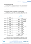
1
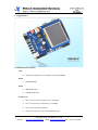
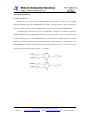
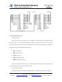
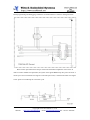
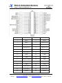
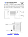
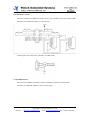
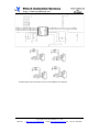
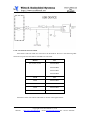
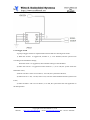
FL2440 Users Manual
Copyright@2010-2011
http://www.arm9board.net
Website:
Copyright reserved© Witech Co., Ltd.
http://www.arm9board.net Email: [email protected] Tel: +86-871-5899845
COPYRIGHT STATEMENT
Contents (content being images, text, programs and scripts)
of this manual is copyright © Witech Co., Ltd. All rights
expressly reserved.
Any content of the manual printed or downloaded may not be
sold, licensed, transferred, copied or reproduced in whole or in part
in any manner or in or on any media to any person without the prior
written consent of Witech Systems Ltd. including but not limited to:
z transmission by any method
z storage in any medium, system or program
z display in any form
z performance
z hire, lease, rental or loan
Requests for permission to reproduce material from this manual
should be addressed to Witech Systems Ltd.
Website:
Copyright reserved© Witech Co., Ltd.
http://www.arm9board.net Email: [email protected] Tel: +86-871-5899845
FL2440 is a development board released by Witech Embedded for the Samsung S3C2440; it
is split into two parts: 6-layer core board and a 2-layer application board, such structure not only
makes the FL2440 more flexible and also more convenience for maintenance. The layout and
wiring on the FL2440 are professionally designed, to make the FL2440 development board more
stable and reliable performance. Together with the FL2440 we provide BSPs (Board Support
Packages) for Embedded Linux and WindowsCE including basic drivers for all the components on
the board and illustrating programs, which we believe can help the users in understanding the
ARM architecture and shortening their development circle.
Here are some dos and don’ts for using the FL2440:
1. After opening the FL2440 package, please check and make sure that the following
components are all enclosed:
2.
3.
4.
5.
6.
z 1 × FL2440 board
z 1 × serial port cable
z 1 × USB cable
z 1 × Ethernet cable
z 1 × JTAG wiggler with JTAG cable
z 1 × 5V power supply
z 1 × DVD
After purchasing the FL2440, please do inform us with your purchase information,
including your name, registered email address, purchase date, invoice number and
board ID to validate your membership for downloading the latest data from our website.
When using the development board for the first time, please do read and follow the user
manual to prevent unnecessary troubles and damages.
Every time before powering on the development board, please touch anyone of the
metallic interface with your fingers to unload the Electrostatic. Do not touch the chips
with your fingers!
Before physically operating the development board, please switch the power off. Hot
plugging is NOT supported except on the USB and Ethernet interfaces.
We provide for the FL2440 12 weeks’ guarantee (in the precondition of non-artificial
damage) and 24 weeks technical support.
Editor: Witech Co. Ltd.
Tel: 86-871-5899845
Fax: 86-871-5899845
Email: [email protected]
Website: http://www.arm9board.net/
Website:
Copyright reserved© Witech Co., Ltd.
http://www.arm9board.net Email: [email protected] Tel: +86-871-5899845
Chapter One: Hardware Introduction
The FL2440 Development board consists of a 6-layer core board and a 4-layer application
board. Layout and wiring on the FL2440 is meticulously designed by professionals to ensure
stable performance, which, together with a variety of interfaces, connectors, and ports, makes the
FL2440 a reliable device for the development of hand-held device, consumer electronics and
Industrial control equipment.
1.1 Components in the Package
Standard Components:
1.
1 × FL2440 board
2.
1 × serial port cable
3.
1 × USB cable
4.
1 × Ethernet cable
5.
1 × JTAG wiggler with JTAG cable
6.
1 × 5V power supply
7.
1 × DVD
Optional Components:
1.
3.5” TFT LCD with touch panel and stylus.
2.
5.7” TFT LCD with touch panel and stylus.
3.
7” TFT LCD with touch panel and stylus.
4.
OV9650 CMOS camera
5.
USB camera
6.
WIFI module
1.2 DVD contents
The DVD includes some documents and development resources for the FL2440
development board. In the DVD:
♦
The folder named as “bootloader” contains the source code and object files of the
bootloader.
Website:
Copyright reserved© Witech Co., Ltd.
http://www.arm9board.net Email: [email protected] Tel: +86-871-5899845
♦
Folder “Linux” contains kernel source code, filesystem and some related tools for
Linux-2.6.12 and Linux-2.6.28.
♦
Folder “WinCE” contains the WindowsCE BSP source code, SDK, test program and
binaries.
♦
Folder “ucos2” contains the source code and binaries of ucos2 operating system.
♦
“Drivers” contains USB driver, parallel port driver, JLINK driver, ActiveSync driver
and USB-RS232 driver for the PC.
♦
“Schematics” contains the schematic of the FL2440 application board and layout of the
core board.
♦
“Demos” contains demonstration programs.
♦
“Tools” contains some utility programs such as DNW, H-JTAG, ActiveSync.
♦
“Datasheets” contains datasheets for the major on-board components and chips.
♦
“HardwareTest” contains the source code and binaries for the hardware test program.
♦
“Manuals” contains user manuals and operation instructions in PDF.
Website:
Copyright reserved© Witech Co., Ltd.
http://www.arm9board.net Email: [email protected] Tel: +86-871-5899845
1.3 Appearance
1.4 Hardware Resources
CPU:
¾
Samsung S3C2440A microcontroller, running @400MHz
RAM:
¾
64MB SDRAM
Flash:
¾
4MB NOR Flash
¾
256MB Nand Flash
Serial Ports:
¾
One 5-wire serial ports, baud rate @ 115200bps;
¾
One 3-wire serial port, baud rate @ 115200bps;
¾
One-3-wire expansion interface;
¾
The three serial ports can be used simultaneously.
Website:
Copyright reserved© Witech Co., Ltd.
http://www.arm9board.net Email: [email protected] Tel: +86-871-5899845
Ethernet Ports:
¾
One 100M Ethernet with connection and transmission indicator, using DM9000
USB Interfaces
¾
Four USB1.1 Host interfaces
¾
One USB1.1 Device interface
Audio:
¾
One stereo audio output socket for earphone or speaker, using IIS interface chip
UDA1341
Storage Interfaces:
¾
One SD card slot
LCD&Touch Interface:
¾
On-board 4-wire resistive touch screen interface
¾
One 40-pin LCD connector
¾
Support black and white, 4 level grayscale, 16 level grayscale, 256-color,
4096-color STN LCD
Camera connector:
¾
One 20p 2.0mm pitch camera connector
Clock source:
¾
Built-in real time clock
Reset Circuit:
¾
One reset button with specific reset chip
JTAG Interface:
¾
One 20pin Multi-ICE JTAG interface, supporting SDT2.51, ADS1.2
Power Supply:
¾
5V power supply with power switch and indicator
Others:
¾
Website:
Four user buttons
Copyright reserved© Witech Co., Ltd.
http://www.arm9board.net Email: [email protected] Tel: +86-871-5899845
¾
Four user LEDs
¾
One PWM controlling buzzer
¾
One adjustable resistance connected to ADC pins for A/D conversion
¾
One infrared receiver (optional)
¾
One temperature sensor (optional)
Website:
Copyright reserved© Witech Co., Ltd.
http://www.arm9board.net Email: [email protected] Tel: +86-871-5899845
1.5 Hardware Resource Distribution
1.5.1 Address Space and Chip Selection
The FL2440 can be boot from either Nand Flash or NOR Flash. The distribution of storage
space is different when booting from each Flash, as shown in the figure below:
The left drawing is the memory allocation diagram when the system is set to the Nor
Flash boot mode with nGCS0 being set.
The right drawing is the memory allocation diagram when the system is set to the
Nand Flash boot mode.
Note: SFR Area is reserved for special registers
nGCS0 will map its address space to different devices when the system boots in
different modes
- When the system boots from the Nand Flash, its 4K Bytes BootSram will be
mapped to nGCS0’s address space;
Website:
Copyright reserved© Witech Co., Ltd.
http://www.arm9board.net Email: [email protected] Tel: +86-871-5899845
- When the system boots from the Nor Flash (not the Nand Flash boot mode), the
Nor Flash which is connected to nGCS0 will be mapped to nGCS0’s address space.
SDRAM address space: 0x30000000 ~ 0x34000000
1.5.2 On-board Interfaces
Interface
Description
PHONE
Audio Output Interface (PHONE)
MIC
Audio Input Interface (MIC)
CON4
LCD/Touch Interface
JP1
Camera interface
CN2
Standard 20pin JTAG interface
POWER
Power socket
J9
GPIO interface
CON1, CON2
Core board connector
CON5
4-channels AD
Button
Description
S1(RESET)
Reset button (Black)
S2, S3, S4, S5
Four user buttons (Red)
1.5.3 Buttons
1.5.4 LEDs
LED
Description
LED0, LED1, LED2, LED3
I/O indicator
Website:
Copyright reserved© Witech Co., Ltd.
http://www.arm9board.net Email: [email protected] Tel: +86-871-5899845
Website:
LED5
5V power status indicator
LED9
Core board 3.3V power supply indicator
Copyright reserved© Witech Co., Ltd.
http://www.arm9board.net Email: [email protected] Tel: +86-871-5899845
1.6 Major Hardwares
1.6.1 Storage Devices
Storage devices on the FL2440 include SDRAM and Flashes, consists of two 32MB
Samsung SDRAM chips, one 256MB Nand Flash chips. In order to improve the communication
efficiency with the CPU, the 32bit SDRAM system consists of two half-word SDRAM chips.
Considering the actual needs of users’, the SDRAM is designed as compatible, supporting
32MB or 64MB single chip SDRAM controlled by the two resistances shown in the figure below.
As shown in the figure, for using 32MB SDRAM we should connect the pin2 and pin1 on the R32
with 22Ω resistance, and also connect the pin2 and pin3 on R33 with 22Ω resistance; for using
64MB SDRAM we should connect the pin3 and pin2 on the R32 with 22Ω resistance, and also
connect the pin1 and pin2 on R33 with 22Ω resistance;
Website:
Copyright reserved© Witech Co., Ltd.
http://www.arm9board.net Email: [email protected] Tel: +86-871-5899845
1.6.2 JTAG and Reset Logic
a) What is JTAG?
JTAG (Joint Text Action Group) was a standard for testing PCB and integrated circuit
formed in 1985; in 1990 it became an IEEE standard as IEEE 1149.1-1990, it was used for
boundary scanning and fault detecting on hardware circuits with JTAG-interfaced ICs. Normally, a
JTAG interface should include the following pins:
1. TDI (Test Data In)
2. TDO (Test Data Out)
3. TCK (Test Clock)
4. TMS (Test Mode Select)
5. TRST (Test Reset) optional.
JTAG was initially formed to test ICs, in nowadays; JTAG interface is also used a lot for ISP
(In System Programming) to program Flash and etc.
b) JTAG on the FL2440
JTAG interface on the FL2440 development board is a standard 20-pin interface, supports
Website:
Copyright reserved© Witech Co., Ltd.
http://www.arm9board.net Email: [email protected] Tel: +86-871-5899845
Flash programming and debugging. Schematic of JTAG interface is shown in the figure below.
Reset circuit: Specialized reset chip is used on the FL2440 to implement reset circuit. In
order to ensure reliable reset operation, the system reset signal nREST keep low power level for 4
clock cycle. Once an external reset signal is received by the CPU, it will turn the CPU reset signal
to low power level and keep for 128 clock cycle.
Website:
Copyright reserved© Witech Co., Ltd.
http://www.arm9board.net Email: [email protected] Tel: +86-871-5899845
1.6.3 LCD/Touch Screen interface
Website:
Pin
Function
Pin
Function
1
VCC
2
VCC
3
VD0
4
VD1
5
VD2
6
VD3
7
VD4
8
VD5
9
VD6
10
VD7
11
GND
12
VD8
13
VD9
14
VD10
15
VD11
16
VD12
17
VD13
18
VD14
Copyright reserved© Witech Co., Ltd.
http://www.arm9board.net Email: [email protected] Tel: +86-871-5899845
19
VD15
20
GND
21
VD16
22
VD17
23
VD18
24
VD19
25
VD20
26
VD21
27
VD22
28
VD23
29
GND
30
LCD_POWEN
31
—
32
—
33
VM
34
VFRAME
35
VLINE
36
VCLK_L
37
TSXM
38
TSXP
39
TSYM
40
TSYP
1.6.4 Ethernet Interfaces
Schematic of the 10M Ethernet circuit is as shown in the figure below:
Website:
Copyright reserved© Witech Co., Ltd.
http://www.arm9board.net Email: [email protected] Tel: +86-871-5899845
1.6.5 GPIO Interface
There are 30pins on the GPIO interface, two of which are SPI interface, one is IIC interface
four AD channels and others are IOs for general purpose.
Website:
Copyright reserved© Witech Co., Ltd.
http://www.arm9board.net Email: [email protected] Tel: +86-871-5899845
Website:
Pin
Function
Pin
Function
1
GPE11
2
GPE12
3
GPE13
4
GPG2/EINT10
5
GPG3/EINT11
6
GPG5/EINT13
7
GPG6/EINT14
8
GPG7/ENT15
9
GPG11/EINT19
10
GPG15/EINT23
11
GPG13/EINT21
12
GPG14/EINT22
13
GPB5
14
GPB6
15
GPB8
16
GPB10
17
NRSTOUT/GPA21
18
GPB7
19
AIN0
20
AIN1
21
AIN2
22
AIN3
23
EINT0/GPF0
24
EINT2/GPF2
25
EINT3/GPF3
26
EINT4/GPF4
27
IICSDA
28
IICSCL
Copyright reserved© Witech Co., Ltd.
http://www.arm9board.net Email: [email protected] Tel: +86-871-5899845
29
VDD33V
30
GND
1.6.6 SD card slot
The SD card slot on the FL2440 supports up to 2GB SD card. Schematic of the SD card slot
is shown as below:
About SD card:
Secure Digital (SD) is a non-volatile memory card format developed by Panasonic, SanDisk,
and Toshiba on the basis of MultiMedia Card (MMC) format for use in portable devices. Currently
it is widely used in digital cameras, digital camcorders, handheld computers, netbook computers,
PDAs, media players, mobile phones, GPS receivers, and video games. Standard SD card
capacities have a maximum of 2 GB. With a physical profile of 24 mm × 32 mm × 2.1 mm, the
new card provided both DRM up to the SDMI standard, and a high memory density for the time.
1.6.7 IIS Audio I/O Interface
IIS, also known as Inter-IC Sound, Integrated Interchip Sound, or I2S, is an electrical
serial bus interface standard used for connecting digital audio devices together. It is most
commonly used to carry PCM information between the CD transport and the DAC in a CD player.
As shown in the schematic below, on the FL2440 the IIS Bus is connected to the PHILIPS audio
digital signal decoder UDA1341TS and then lead out the MIC audio input channel and SPEAKER
Website:
Copyright reserved© Witech Co., Ltd.
http://www.arm9board.net Email: [email protected] Tel: +86-871-5899845
audio output channel. The IIS interface on the S3C2440X01 micro-controller is connected to the
BCK, UWS, DATAI SYSCLK. L3 bus on the UDA1341TS works only when the microcontroller
inputs, it includes L3DATA, L3MODE and L3CLOKE, respectively the microcontroller interface
data, microcontroller interface mode, and microcontroller interface clock, via which the
microcontroller is able to configure the DSP (Digital Signal Processing) parameters and system
controlling parameters.
1.6.8 Camera Interface
A 20-pin 2.0mm pitch connector is implemented on the FL2440 as camera connector.
Schematic of the camera interface is shown in the figure below:
Website:
Copyright reserved© Witech Co., Ltd.
http://www.arm9board.net Email: [email protected] Tel: +86-871-5899845
1.6.9 Serial Port Circuit
There are two RS232 (COM0 and COM1) and one TTL (COM2) serial ports on the FL2440.
Schematic of COM0 and COM1 is as shown below:
And the figure below shows the schematic of COM2 (TTL):
1.6.10 USB Interfaces
There are Four USB Host interfaces and one USB Device interface on the FL2440:
Schematic of USB Host interface is shown in the figure:
Website:
Copyright reserved© Witech Co., Ltd.
http://www.arm9board.net Email: [email protected] Tel: +86-871-5899845
And the figure below shows the circuits on the USB Device interface:
Website:
Copyright reserved© Witech Co., Ltd.
http://www.arm9board.net Email: [email protected] Tel: +86-871-5899845
1.6.11 User buttons and User LEDs
Four buttons and four LEDs are reserved on the FL2440 for the users. The following table
shows the I/O ports that the buttons and LEDs are connected:
Button
I/O
S2, S3, S4, S5, S6
EINT0/GPF0
EINT2/GPF2
EINT3/GPF3
EINT4/GPF4
LED
I/O
LED1
EINT3/GPF3
LED2
EINT4/GPF4
LED3
EINT5/GPF5
LED4
EINT6/GPF6
Schematics of the user buttons and LEDs are shown in the figures below:
Website:
Copyright reserved© Witech Co., Ltd.
http://www.arm9board.net Email: [email protected] Tel: +86-871-5899845
Website:
Copyright reserved© Witech Co., Ltd.
http://www.arm9board.net Email: [email protected] Tel: +86-871-5899845
1.6.12 AD Convert
The S3C2440 microcontroller provides 8-channels 10bit AD conversion interfaces (among
which four channels are used for the touch screen), with Differential Linearity Error limited to ±
1.0 LSB, and Integral Linearity Error limited to ± 2.0 LSB.
On the OK2440-II, an adjustable resistance is implemented for testing AD conversion. The
circuit of the resistance is shown in the figure below:
1.6.13 Infrared Receiver
Website:
Copyright reserved© Witech Co., Ltd.
http://www.arm9board.net Email: [email protected] Tel: +86-871-5899845
1.6.14 Temperature Sensor
1.6.15 IIC (24C02)
Website:
Copyright reserved© Witech Co., Ltd.
http://www.arm9board.net Email: [email protected] Tel: +86-871-5899845
1.6.16 Toggle Switch
A group of toggle switches is implemented on the FL2440 for selecting boot modes:
1) When the switch 1 is toggled off, switches 2, 3, 4 are disabled, and the system boots
according to the bootloader settings;
When the switch 1 is toggled On, the bootloader settings will be disabled
2) When the switch 1 is toggled On while switches 2, 3, 4 are Off, the system enters the
bootloader menu;
3) When switches 1 and 2 are On while 3, 4 are Off, the system boots WinCE;
4) When switch 1 is On, 2 is Off, and 3 is On, switch 4 will be disabled and the system boots
Linux;
5) When switches 1 and 4 are On while 2, 3 are Off, the system boots the user application in
the APP partition.
Website:
Copyright reserved© Witech Co., Ltd.
http://www.arm9board.net Email: [email protected] Tel: +86-871-5899845
1.7 Board Support Packages
Together with the FL2440 development board we provide Board Support Packages for
WinCE and Embedded Linux.
1.7.1 Embedded Linux
♦
Kernel: Linux-2.6.12 and Linux-2.6.28
♦
Supported Filesystem: cramfs/ramfs/etx2/fat32/nfs/yaffs2/jffs2
♦
Drivers included:
♦
9
System interrupt and system clock driver
9
Serial device driver
9
Block device (IDE hard disk, SD card) drivers
9
Nand Flash driver
9
Ethernet driver
9
RTC driver
9
USB Host driver
9
LCD driver
9
Touch screen driver
Busybox commands:
cat,chmod,discard,echo,flashfsd,flashwrite, free,genhtml,hostname,init,
kill,loader,ls,mkdir,mount,ps,reboot,rm,smanaged,sysconf, yes,insmod,
lsmod,rmmod
♦
Graphical Interface: Qtopia provided as source code. Other GUIs such as MIZI,
microwindows, minigui and etc are also supported.
♦
Ethernet service: web server, ftp, telnet
♦
Applications: MP3 player and etc.
♦
Ethernet protocol: complete TCP/IP
1.7.2 WinCE
♦
Version: WindowsCE 5.0/WinCE6.0
Website:
Copyright reserved© Witech Co., Ltd.
http://www.arm9board.net Email: [email protected] Tel: +86-871-5899845
♦
Drivers:
9
System interrupt and system clock driver
9
Serial device driver
9
Block device (SD card) drivers
9
Nand Flash driver
9
Ethernet driver
9
RTC driver
9
USB Host driver
9
USB Slave
9
LCD driver
9
Touch screen driver
♦
Ethernet protocols: standard IPV4 protocols including TCP/IP, UDP, SMTP, etc.
♦
Display: supporting LCD/VGA/TV displaying
♦
Applications: IE, MediaPlayer, etc
♦
Other WinCE standard functions
Website:
Copyright reserved© Witech Co., Ltd.
http://www.arm9board.net Email: [email protected] Tel: +86-871-5899845