1
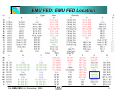
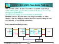
EMU FED
--- Crate and Electronics
B. Bylsma, S. Durkin, Jason Gilmore, Jianhui Gu, T.Y. Ling
The Ohio State University
ESR, CERN, November 2004
EMU FED: Outline
• EMU FED Design
• FED Crate & Custom Backplane
• DDU Functions and Tests
• DCC Functions and Tests
• Data Flow Control
• FED Production Preparation
GU, EMU FED ESR, November, 2004
2
EMU FED: EMU FED Design
Gb/s Fibers
Myrinet
5Gb/s Fibers
SLINK64
CMS
DAQ
TMB
Peripheral
DMB
CFEB
FRL
FED
USC55
ALCT
AFEB
Detector
GU, EMU FED ESR, November, 2004
540 DMB as inputs (160MB/s)
8 SLINK64 as outputs (800MB/s)
Expected data rate 1.2 GB/s
3
EMU FED: EMU FED Location
GU, EMU FED ESR, November, 2004
4
EMU FED: EMU FED Design
• Four 9U Crates
9U X 220mm Board
• Data Concentration:
D
C
C
DDU
15 DMB to 1 DDU
9 DDU to 1 DCC
1 DCC to 2 SLINK64
DDU
9 DDU per SLINK (4)
4/5 DDU per SLINK (8)
2/3 DDU per SLINK (16)
1 DDU per SLINK (36)
36 DDU, 4/8 DCC needed
Base-line design
Optional
The crate will be a standard 9U crate with minor modification
GU, EMU FED ESR, November, 2004
5
EMU FED: EMU FED crate backplanes
P1: Standard VME64x, for slow control
P2: empty
P3: custom for TTC control and Fast data transmission between DDU and DCC
6.4 Gbps rated connector
Data from DDU to DCC
TTC control bus
GU, EMU FED ESR, November, 2004
6
EMU FED: DDU Prototype
VME FPGA
DMB Input FPGAs
4 Input FIFOs
GBE FIFO
XILINX Virtex2-500
2 XILINX Virtex2Pro-20
512 KB each
1024 KB
9U VME
board,
220 mm
depth
FMM
output port
15 Optical
fiber inputs
(just 1 for now)
DDU Control FPGA
Gbit Ethernet
Output
XILINX Virtex2Pro-7
To Local DAQ
GU, EMU FED ESR, November, 2004
SLINK
Mezzanine board
connector
7
EMU FED: DDU Plan
FMM & Slow Control
VME
FPGA
FIFO
FPGA
FPGA
FIFO
Transceivers
GU, EMU FED ESR, November, 2004
TTC control
from DCC via
backplane
MGT-HSC
Fiber links from 15 DMBs
FPGA
•BUSY
•READY
•L1 Throttle
•Data Errors
•Loss of Synch
Slow-control
and JTAG
DCC/DAQ
Multi-Gigabit
Transmission
via HighSpeed
Connector to
backplane
S-Link
(for SP use)
Gigabit Ethernet
To Local DAQ
8
EMU FED: DDU Design (1)
• DDU Functions
– High-Bandwidth data concentration and buffering
• 13 DMB B DAQ via DCC, capable of continuous 600+ MB/sec rate
• Parallel data readout via Gigabit Ethernet (local DAQ path)
– Full error checking and status monitoring
• CRC check, word count, L1 number, BXN, overflow, link status
– FMM communication path for EMU DAQ
• DAQ Buffer capacity
– Average EMU occupancy is ~3 CSCs with data per event at LHC
• 8 Byte event header sent from DMB for empty “no data” events
– Headers from empty events are zero-suppressed at DDU
• A typical DDU “data event” has 3 kB at LHC
• Average event size in the DDU is 450 Bytes
– Each DDU has 2.5 MB buffer: 20% in FPGA BRAM, 80% in FIFO
• Typically enough to hold 2000 events at LHC
• Typical event process time ~1 µsec
GU, EMU FED ESR, November, 2004
9
EMU FED: DDU Design (2)
• TTC clock & control from DCC via backplane
• Slow control via VME
– Provides link to on-board serial/JTAG paths
• Load firmware into on-board EPROMs
• Load constants into on-board Flash memory
– Warning thresholds, offsets and Board ID
– Provides path for system-wide status monitoring
• VME Controller can see “global overview” of all 36 DDUs
• Allows fast detection/response for subtle effects
GU, EMU FED ESR, November, 2004
10
GU, EMU FED ESR, November, 2004
11
EMU FED: DDU Performance
• Oct. 2004 Beamtest results: no problems
– Multiple DMB readout to DAQ
• Good performance via DCC/S-Link and gigabit Ethernet spy
path
– Error-free operation at high rates
• Muon rates at H2 beam up to 25 kHz
• Passed all tests at 9-times LHC expected data rate
• DDU buffer size is more than sufficient for LHC
– Status/error monitoring
• All checks performed as expected, verified in offline software
• Verified consistent fast monitoring path performance
GU, EMU FED ESR, November, 2004
12
EMU FED: DDU Testing Procedure
• Receive board from assembly house
• Load the VME_FPGA PROM
• Load the DDU_Ctrl PROM
• Load the InFPGA PROM
• Read in the board ID from PROM user code
• Every time after RESET, the DDU will be in a ready state
• Before LHC run, download a BX_Number offset through VME
slow control, so the BX_number will match between DDU,
DMB and other peripheral crate electronics
• EMU needs 36 DDUs plus spares
GU, EMU FED ESR, November, 2004
13
EMU FED: DCC Function
Each DCC serves 1/4 of EMU
9 DDU, 2 SLINK64
Data Concentration
•
Merge 10 DDUs data into two slink64,
two optional gigabit spy path
Fast Control
•
•
Receive TTC fiber signals using
TTCrx, send L1A CMS_clock and
other TTC command to FED crate
Optional FMM interface
Slow Control
• VME Slave
Misc.
•
•
•
GU, EMU FED ESR, November, 2004
9U x 220mm VME slave
+5V (<1A), +3.3V (~6A)
Regulators for +2.5V, +1.5V, +1.5V
14
EMU FED: DCC Data Acquisition
DDU0
DDU1
DDU2
3.2Gb/s
160MHz
x2
3.2Gb/s
x 40
IN_FPGA
3.2Gb/s
VME 64X
FIFO1
Em e rge ncy
160MHz
x 40
x2
FIFO2
IN_FPGA
3.2Gb/s
DDU3
DDU4
1Gb/s
160MHz
x2
x 40
3.2Gb/s
FIFO3
160MHz
x2
x 40
125MHzDDR
FIFO4
x 40
DDU6
3.2Gb/s
FIFO5
x 40
160MHz
x 40
x2
3.2Gb/s
x 40
x2
x 64
3.2Gb/s
FIFO6
160MHz
x2
x 40
3.2Gb/s
160MHz
DDU8 x 2
DDU9
3.2Gb/s
x2
x 40
FIFO7
FIFO8
IN_FPGA
100MHz
FIFO
125MHz
x 64
1Gb/s
IN_FPGA
DDU7
125MHz
125MHzDDR
160MHz
Gigabit ethernet
SLINK64
x 64
M_FPGA
IN_FPGA
DDU5
Power
160MHz
x 40
x2
FIFO0
100MHz
FIFO
SLINK64
x 64
Gigabit ethernet
L1A
CMSCLK
control
V ME
control
FMM
160MHz
x 40
FIFO9
GU, EMU FED ESR, November, 2004
Backplane
TTCrx
TTC
15
EMU FED: DCC Few Extra features
9Mb FIFO to buffer the data from FPGA to SLINK transmitter:
• This will keep the speed on data readout at 1GByte/s, and SLINK
throughput at 800MByte/s
• It serves as a storage, to even out the L1A fluctuation
DDR FIFO keeps the same data rate using less number of wires.
The DCC has the ability to combine the two sets of FIFO inputs and
send the data to one SLINK transmitter.
Data transmission backpressure:
DMBFIFO
FIFO
DDU
FIFO DCC
FIFO
SLINK
TTS
GU, EMU FED ESR, November, 2004
16
EMU FED: Data Back pressure
When Slink is full, the DCC will stop sending data to Slink, the data
will be buffered at the DCC S_FIFO,
When the DCC S_FIFO is ‘Almost_full’, it will stop the DCC
assembling events. The data will backup on the IN_FIFO;
When the IN_FIFO gets to a certain point, it will backpressure on
DDU, the DDU will stop sending data to DCC. The data will be
backup on DDU;
When DDU FIFO get to a certain point, it will backpressure the DMB,
and send warning signals through FMM to TTS.
If the DMB FIFOs will be monitored by DDU, and the DMB can also
disable the trigger sending to CFEB in case the DMB FIFO close to
full.
If the TTS does not respond to DDU warning, the DDU will send data
to DCC to prevent DDU FIFO get full, the DCC will only receive and
process data header/trailer to prevent FIFO get full, and at the same
time, keep the data package integrity.
This mechanism should give sufficient time for TTS to respond.
GU, EMU FED ESR, November, 2004
17
EMU FED: DCC Data Acquisition
On L1A (Data is always sent on L1A)
DDU sends data to DCC asynchronously (relative to L1A)
DCC assembles data from DDUs into events and sends to FRL asynchronously
LV1_ID(24), Bx_id(12) and Orbit_ID(32) are used to identify the event
EMU DCC Event Size: no data ~300 bytes
1 CFEB ~3 Kbytes
5 CFEB ~10Kbytes
Average ~2 Kbytes
max_size 800 Kbytes
DCC Data format:
63…60 59..56 55……………………………….32 31……………20 19……………8 7…4 3..1 0
Header 1: K 5
| Evty |
LV1_ID (24)
| Bx_id (12)
| source_id |FOV|Hx$$
Header 2: K D
| 9 |
Orbit_ID (32)
| FIFO_stat(16)
| 9 | 7
Data Load D
……………………………
Data Load D
……………………………
……………….
Data Load D
…………………………….
Trailer 2: K E
| F | D_time(8) | DDU4(8) | DDU3(8) | DDU2(8) | DDU1(8) | DDU0(8) | FIFO_s(8)
Trailer 1: K A | X
|
Evt_lgth(24)
| CRC(16)
| X | Evt_S| TTS| Tx$$
GU, EMU FED ESR, November, 2004
18
EMU FED: DCC Slow Control
VME A24/D16 in VME64X P1 Backplane
• A[23:19] match with GA[4:0] for specific slot, broadcast.
• A[18:12] is used to address the different slow control paths (devices)
• A[11:1] are specific to the given device
A[18:12] device definition:
00: VME registers on the FPGA
02: JTAG for Controller PROMs
03: JTAG for IN_FPGA’s PROM
04: JTAG for IN_FPGA
05: JTAG for SLINK_A
06: JTAG for SLINK_B
07: TTCrx I2C interface
0F: Emergency load for Controller PROMs
The DCC are always VME controllable even after FPGA
ISPROM get SEU
GU, EMU FED ESR, November, 2004
19
EMU FED: DCC Fast Control
Custom Backplane carries all Fast control Signal
Fast control signals TO the backplane (Bus_LVDS):
•
TTCrx on board, automatically select the TTC clock or the on-board
oscillator as 40MHz source, four segments on the backplane
•
Automatically select TTC L1A, command bus or on board VME
generation
•
The command bus and Data bus are switched, depending on the
command_bus_strobe and Data_bus_strobe
•
Summary of backplane signals: Clock, L1A, Command_Strobe,
Data_Strobe, Cmd_Dat_Bus(8), Hard_reset
Fast control signals FROM the backplane (Bus_LVDS):
•
Clock, L1A, Command_Strobe, Data_Strobe, Cmd_Dat_Bus(8)
Only one DCC is enabled for control signals to the backplane
GU, EMU FED ESR, November, 2004
20
EMU FED: DCC Structure Beam Test
Sept/Oct. 2004, H2 beams
• TTC control – no issues
• Backplane communications
– no issues
• Synchronization – no issue
DCC rate tests carried out with high trigger rate.
– 100 KHz L1A (TTCvi random trigger), >100 KHz LCT (lowering the
comparator threshold to 2mV), FakeDDU sends 2.3KB per L1A, The DDU
sending five chambers data, this gives >240MB/s data rate to SLINK.
Check the L1A_number, Event size, 1/1000 write to disk and check
synchronization offline. No Problem on DCC.
GU, EMU FED ESR, November, 2004
21
EMU FED: DCC tests: Some issues
On the DDR FIFO, there are internal cross talk from D22 to D21
line. Get around: do not use D21, we only need 33 bits out of
40bits on the FIFO.
The DDR FIFO works at 125MHz reading speed, but the
manufacture downgraded its rating to 100MHz. Solution: Even
100MHz (800MB/s) is good enough for our application (Slink
~200MB/s)
At the CERN beam test, we do not have a readout system fast
enough to handle the 200MB/s data, required by SLINK, this is
not a real problem.
GU, EMU FED ESR, November, 2004
22
EMU FED: DCC Bench test
By plugging the DDU in different slot of the FED
crate, all the ten DCC inputs are tested, and the
two slink outputs are tested.
Because the FED crate are in underground
counting house, there is no need for radiation
test and magnetic test !
GU, EMU FED ESR, November, 2004
23
EMU FED: DCC procedures
• VME emergency load the Main_FPGA PROM
• VME load the IN_FPGA PROM
• The FPGA read in the board ID from PROM usercode
• Load in the channel enable (DDU_in_use)
• Every time after RESET, the DCC will be in a ready state
• During LHC run, download a BX_number offset through
VME slow control, or set the delay on the TTCrx, so the
BX_number will match between DCC, DDU and
peripheral crate electronics.
GU, EMU FED ESR, November, 2004
24
EMU FED: Production preparation
•How many boards do we need?
DDU
DCC
DDU needed
36 + 1
Total (+ 20% spare)
45
4/5/9 DDU per Slink
4
( 2/3 DDU per Slink
8 )*
spare boards
2
Total boards producing
10
* This is just for very high data rate, requires 16 SLINK64
•The Ohio State University will maintain the DDU and DCC
•some spare parts will be ordered in addition to the spare
board for anticipated repair
GU, EMU FED ESR, November, 2004
25
EMU FED: Production Test
PC boards will be etched and stuffed commercially
Boards will be measured and debugged on computerized tester before
and after burn-in at OSU
Each board will have a unique ID
Board tracking: Microsoft Access
To test the DDU:
-Read DAQMB will be used as DDU input source, DCC as output destination
-Check all inputs by moving fiber from connector to connector
-Check Gigabit readout (spy path) by computer readout
To test the DCC:
-DDU signals mimicked by ‘fakeddu’
-Check all inputs by moving ‘fakeddu’ from slot to slot
-Check all outputs by moving SLINK transmitter card
After we have enough DDUs, the full FED crate will be tested
GU, EMU FED ESR, November, 2004
26
EMU FED: Production Burn in
Burn In
CDF: 50-60 C for 8-24 Hrs
Sufficient for tantalums failures
No sensitivity to semiconductor
failure
US Military: 125 C for 320 Hrs
Chip Makers recommend against this
CFEB, DAQMB: 65 C for 24 Hrs
Prove to be effective, not damaging
Each DDU/ DCC: 65C for 24 Hrs
Test Before and After
GU, EMU FED ESR, November, 2004
27
EMU FED: Production Validation
-First DDU was made in Jun. 2002
-Redesigned DDU was made in Jan. 2004
-Both boards are working reliably.
-First DCC was made in Jan. 2004
-Second DCC was made in April 2004 with minor change
-Both boards are working.
The full production will be procured after full FED crate test
DDU, DCC Meet Design Specifiations!
We are ready to procure the DDU and DCC
At The Ohio State University
GU, EMU FED ESR, November, 2004
28
EMU FED: DDU & DCC Documentation
http://www.physics.ohio-state.edu/~cms/ddu/
What is it?
EMU DDU details
DDU Operation
General Hardware Info
Technical Operation Details
DDU Data Format
http://www.physics.ohio-state.edu/~cms/dcc/
DCC User's Manual
DCC ESR at CERN (Powerpoint)
DCC PCB schematic design (pdf)
DCC Data receiver FPGA design (latest version .svf) (pdf)
DCC Slink interface FPGA design (latest version .svf) (pdf)
DCC Output (Slink, Gigabit Ethernet) data format
GU, EMU FED ESR, November, 2004
29