1
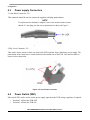
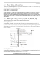
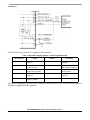
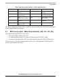
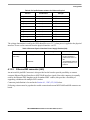
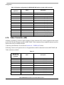
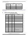
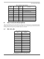
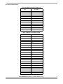
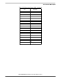
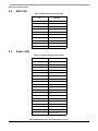
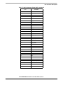
Freescale Semiconductor User Manual Document Number: MPC5604EEVB64UM MPC5604EEVB64 Evaluation board User Manual For MPC5604E Evaluation/Validation by: Pavel Bohacik MSG Application Engineering 1 Introduction The MPC5604EEVB64 Evaluation Board (EVB) is based on the e200z0 Power Architecture®. This board is shipped with the PPC5604EEMLH 64-pin LQFP MCU populated to allow the evaluation of the full functionality of this part. This board is designed as a validation platform with the maximum flexibility. Where possible it is also designed for power and speed but the primary goal of this system is to allow main usecases of this processor. 2 References • • MPC5604ERM Reference Manual MPC5604E Data Sheet © Freescale Semiconductor, Inc., 2011. All rights reserved. Contents 1 2 3 4 5 6 7 Introduction . . . . . . . . . . . . . . . . . . . . . . . . . . . . . . . . . . . 1 References . . . . . . . . . . . . . . . . . . . . . . . . . . . . . . . . . . . 1 EVB Features . . . . . . . . . . . . . . . . . . . . . . . . . . . . . . . . . 2 Configuration . . . . . . . . . . . . . . . . . . . . . . . . . . . . . . . . . . 2 Default Jumper Summary Table . . . . . . . . . . . . . . . . . . 16 User Connector Descriptions. . . . . . . . . . . . . . . . . . . . . 18 Known Bugs List . . . . . . . . . . . . . . . . . . . . . . . . . . . . . . 26 EVB Features 3 EVB Features The following is a list of evaluation board features: MPC5604E External Interfaces • Video Encoder Wrapper connected to Omnivision connector • Serial Audio Interface connected to the Audio connector • Onboard Ethernet physical interface plus MII lite connector • Crystal / clock • JTAG • One LIN and one UART interface selectable through Jumper setting • One FlexCAN interface • External Interrupts • ADC connector NOTE Before the EVB is used or power is applied, please read the complete document on how to correctly configure the board. Failure to correctly configure the board may cause irreparable component, MCU or VB damage. 4 Configuration This section details the configuration of each of the EVB functional blocks. Throughout this document, all of the default jumper and switch settings are clearly marked with “(D)” and are shown in blue text. This should allow a more rapid return to the default state of the EVB if required. The EVB is designed with ease of use in mind and is segmented into functional blocks as shown below. Detailed silkscreen legend is used throughout the board to identify all switches, jumpers and user connectors. MPC5604EEVB64 Evaluation board User Manual, Rev. 0 2 Freescale Semiconductor Configuration Figure 1. Evaluation board silkscreen legend 4.1 Processor The MPC5604E processor is the fundamental control chip on the MPC5604EEVB64. This is a version 1 Power Architecture running at a maximum core speed of 64 MHz. The MPC5604EEVB64 allows you to fully evaluate the feature set of the MPC5604E MCU. Refer to Section 3, “EVB Features to review the list of board features. 4.2 Power The EVB requires an external power supply voltage of 12V DC, minimum 1A. This allows the EVB to be easily used in a vehicle if required. The single input voltage is regulated on-board using switching regulators to provide the necessary EVB and MCU operating voltages of 5.0 V, 3.3 V and 1.2 V. For flexibility there are two different power supply input connectors on the EVB as detailed below. MPC5604EEVB64 Evaluation board User Manual, Rev. 0 Freescale Semiconductor 3 Configuration 4.3 Power supply Connectors 2.1 mm Barrel Connector – P4: This connector should be used to connect the supplied wall-plug mains adapter. NOTE If a replacement or alternative adapter is used, care must be taken to ensure that the 2.1 mm plug uses the correct polarization as shown in Figure 2. Figure 2. 2.1 mm Power Connector 2-Way Lever Connector – P1: This can be used to connect a bare wire lead to the EVB, typically from a laboratory power supply. The polarization of the connectors is clearly marked on the bottom site of the EVB. Care must be taken to ensure correct connection. Figure 3. 2-Level Power Connector 4.4 Power Switch (SW1) Side switch SW1 can be used to isolate power supply input from the EVB voltage regulators if required: • Position 1 will turn the EVB OFF • Position 3 will turn the EVB ON MPC5604EEVB64 Evaluation board User Manual, Rev. 0 4 Freescale Semiconductor Configuration 4.5 Power Status—LEDs and Fuse When Power is applied to the EVB, the Green Power LEDs adjacent to 5 V and 3.3 V of the voltage regulators show the presence of the supply voltage. Green LED D9 = 3.3 V for EVB supply Green LED D16 = 5 V for EVB supply If there is no power to the MCU it is possible that either power switch SW1 is in the “OFF” position or that the fuse F1 has blown. The fuse will blow if power is applied to the EVB in reverse-bias, where a protection diode ensures that the main fuse blows rather than causing damage to the EVB circuitry. If the fuse has blown, check the bias of your power supply connection then replace fuse F1 with a 20 mm 2 A fast blow fuse. 4.6 MCU supply routing and Jumpers (J16, J18, J19, J20, J23) The EVB is designed to run the MCU at two supported regulation modes: Internal regulation mode In this mode the I/O supply, Ballast supply and ADC supply are at the same potential of typical 3.3 V (+/- 10%). To reduce power dissipation on the chip, the possibilities of connecting the I/O supply with the Ballast supply via a small resistor 2.5 is being explored. This will lead to the Ballast supply being lower than the I/O supply. Figure 4. Internal regulation mode External regulation mode In this mode, the Ballast supply is shorted to 1.2 V (+/-10%) generated from an external regulator. The I/O supply and the MCU ADC supply continues to be at 3.3 V (+/-10%). MPC5604EEVB64 Evaluation board User Manual, Rev. 0 Freescale Semiconductor 5 Configuration Figure 5. External regulation mode The FlexCAN circuity also has 5 V supplier to the transceiver. Table 1. MCU Power Supply Jumpers – internal regulation mode Power Domain Jumper Position Description 1.2 V J18 (VDD_LV) X This supplies VDD_LV supply pins 3.3 V J19 (V_BALLAST_IN) 1-2 This supplies VDD_S_BALAST supply pin 3.3 V J20 (V_BALLAST_IN_HDR) 2-3 (D) VDD_S_BALAST routed via BALAST resistor 3.3 V J16 (VDD_HV) 1-2 (D) This supplies VDD_HV supply pins 3.3 V J23 (VDD_HV_ADDR) 1-2 (D) ADC reference voltage 3.3 V The jumper configuration shown in Table 1, details the default state (D) of the EVB. In this configuration all power is supplied from the regulators. MPC5604EEVB64 Evaluation board User Manual, Rev. 0 6 Freescale Semiconductor Configuration Table 2. MCU Power Supply Jumpers – external regulation mode Power Domain Jumper Position Description 1.2 V J18 (VDD_LV) 1-2 (D) This supplies VDD_LV supply pins 3.3 V J19 (V_BALLAST_IN) 2-3 (D) This supplies VDD_S_BALAST supply 3.3 V J20 (V_BALLAST_IN_HDR) 2-3 (D) VDD_S_BALAST routed via BALAST resistor 3.3 V J16 (VDD_HV) 1-2 (D) This supplies VDD_HV supply pins 3.3 V J23 (VDD_HV_ADR) 1-2 (D) ADC reference voltage 3.3 V The jumper configuration shown in Table 2, details the default state (D) of the EVB. In this configuration all power supplied from the regulators. 4.7 MCU clock control - Main Clock Selection (J30, J31, J32, J34) EVB supports three possible MCU clock sources: • The local 25 MHz oscillator circuit (Y2) • An 8 MHz Oscillator module (Y1) on the EVB, driving the MCU EXTAL signal • An external clock input to the EVB via the SMA connector, driving the MCU EXTAL signal The clock circuity is shown in the diagram below. Please refer to the appropriate EVB schematic for specific jumper numbers and circuity. MPC5604EEVB64 Evaluation board User Manual, Rev. 0 Freescale Semiconductor 7 Configuration Figure 6. EVB Clock Selection Table 3. Table Clock source jumper selection (J30, J31, J32, J34) Jumper J34 (Y1 PWR) Position PCB Legend FITTED (D) EVB oscillator module Y1 is powered EVB oscillator module Y1 is not powered REMOVED J32 (OSC SEL) Description 1-2 EXTAL-SMA SMA external square wave input 8 MHz Oscillator is routed from Y1 2-3 (D) OSC-MOD J30 Must Match J31 1-2 2-3 (D) Y2 GND MCU clock is Y2 XTALIN GND J31 Must Match J30 1-2 (D) EVB-EXTAL 2-3 Y2 MCU clock is selected by J68 MCU clock is Y2 XTALOUT MPC5604EEVB64 Evaluation board User Manual, Rev. 0 8 Freescale Semiconductor Configuration NOTE The MPC5604E clock circuity is 3.3 V based. Any external clock signal driven into the SMA connector must have a maximum voltage of 3.3 V. 4.8 Reset Boot Configuration (J44, J46, J47) The MPC5604E has 3 boot configuration jumpers (BOOTCFG) that determine the boot location of the MCU based at POR (Power On Reset). This is shown in the Table 4: Table 4. BOOTCFG Control J47 (FAB) J44 (ABS0) J46 (ABS2) Boot ID Boot Mode 1-2 2-3 2-3 — Serial Boot LinFlex without autobaud 1-2 1-2 2-3 — Serial Boot FlexCAN without autobaud 1-2 2-3 1-2 — Serial Boot via LinFlex or FlexCAN in autobaud 2-3 — — Valid SC (Single Chip) 2-3 — — Not Valid Safe Mode 4.9 NEXUS The EVB supports a standard JTAG cable with a 14-pin 0.1” walled header footprint. 4.9.1 Debug Connector Pinouts The EVB is fitted with 14-pin JTAG connector. The following diagram shows the 14-pin JTAG connector pin out (0.1” keyed header). Figure 7. MPC5604E JTAG Connector MPC5604EEVB64 Evaluation board User Manual, Rev. 0 Freescale Semiconductor 9 Configuration NOTE In order to preserve the ability to accurately measure power consumption of the MCU pins, the JTAG connector reference voltages will be sourced directly from the 3.3 V regulator. 4.10 CAN Configuration (J10, J11, J12, J6, J9) The EVB has one NXP TJA1041T high speed CAN transceiver on the MCU CAN channel. This can operate with 3.3 V I/O from the MCU. For flexibility, the CAN transceiver I/O is connected to a standard 0.1” connector and DB9 connector at the top edge of the PCB. Connectors P6 and P3 provides the CAN bus level signal interface for CAN-A. The pin out for these connectors is shown below. Figure 8. CAN physical interface connector MPC5604EEVB64 Evaluation board User Manual, Rev. 0 10 Freescale Semiconductor Configuration Table 5. CAN Control Jumpers (J10, J11, J12, J6, J9) Jumper J11 Position PCB Legend FITTED (D) • 5 V is applied to CAN transceiver VCC • No 5 V power is applied to CAN transceiver REMOVED J12 FITTED (D) • 12 V Power is applied to CAN transceiver VBAT • No 12 V power is applied to CAN transceiver REMOVED J6 FITTED (D) TX • MCU CAN_TXD is connected to CAN controller • MCU CAN_TXD is NOT routed to CAN controller. RX • MCU CAN_RXD is connected to CAN controller • MCU CAN_RXD is NOT routed to CAN controller. WAKE • CAN Transceiver WAKE is connected to GND • WAKE is not connected and available on Pin 2 STB • CAN Transceiver STB is connected to 5 V • STB is not connected and available on Pin 4 EN • CAN Transceiver is Enabled • EN is not connected and available on Pin 6 REMOVED J10 FITTED (D) REMOVED J9 Position 1-2 FITTED (D) REMOVED J9 Position 3-4 FITTED (D) REMOVED J9 Position 5-6 FITTED (D) Description REMOVED Access to the Error and inhibit signals from the transceivers is provided on J14. NOTE You must do the fitting of the jumper headers carefully, as they can easily be fitted in the incorrect orientation. 4.11 RS232 Configuration (J3, J7, J8) The EVB has a single MAX3223 RS232 transceiver device, providing RS232 signal translation for the MCU LINFlex channel. The RS232 output from the MAX3223 device is connected to a DB9 connector, allowing a direct RS232 connection to a PC or terminal. Connector P2 provides the RS232 level interface for MCU SCI (LINFlex). The connector pinout is detailed below. MPC5604EEVB64 Evaluation board User Manual, Rev. 0 Freescale Semiconductor 11 Configuration NOTE The hardware flow control is not supported on this implementation. Figure 9. RS232 Physical Notifies Connector The MPC5604E LINFlex also provides hardware LIN master capability which is supported on the EVB via LIN transceiver. Jumpers J7 and J8 are provided to isolate the MCU LINFlex signals from the RS232 interface as described below. There is also a global power jumper (J3) controlling the power to the RS232 transceiver. Table 6. RS232 Control Jumpers Jumper J3 (SCI-PWR) Position FITTED (D) REMOVED J7 2-3 (D) REMOVED J8 2-3 (D) REMOVED Description • Power is applied to the MAX3223 transceiver • No power is applied to the MAX3223 transceiver • MCU TXD is routed to MAX3223 • MCU TXD signal is disconnected from RS232/LIN • MCU RXD is routed to MAX3223 • MCU RXD signal is disconnected from RS232/LIN The default configuration enables SCI. RS232 compliant interfaces (with no hardware flow control) are available at DB9 connector P2. If the MCU is configured such that SCI is set as a normal I/O port, then MPC5604EEVB64 Evaluation board User Manual, Rev. 0 12 Freescale Semiconductor Configuration the relevant jumpers must be removed to avoid any conflicts occurring. If required, jumper J3 can be used to completely disable the SCI transceiver. 4.12 LIN Configuration (J2, J5, J7, J8) The EVB is fitted with one Freescale MCZ33661EF LIN transceiver. The LINFlex module incorporates a UART mode, and as such, the LIN transceiver are connected to the TX and RX signals of SCI via UART. For flexibility, the LIN transceiver is connected to a standard 0.1” connector (P7) and to one pin molex connector (J1) at the top edge of the PCB as shown in the figure below. For ease of use, the 12 V EVB supply is fed to pin1 of the P7 header and the LIN transceiver power input to pin 2. This allows the LIN transceiver to be powered directly from the EVB supply by simply linking pins 1 and 2 of header P7 using a 0.1” jumper shunt. ** Ensure P7 is added before running LIN as it is not the default on the EVB Figure 10. LIN physical Interface Connector P7 Along with the MCU signal routing jumpers (J7 / J8), there is jumper (J5) to enable or disable the LIN transceiver and jumper (J2) which determines if the LIN transceiver is operating in master or slave mode, as defined in the table below. MPC5604EEVB64 Evaluation board User Manual, Rev. 0 Freescale Semiconductor 13 Configuration Table 7. Jumper J2 Position FITTED REMOVED (D) J5* FITTED (D) REMOVED J7 2-3 (D) 1-2 J8 2-3 (D) 1-2 Description • LIN transceiver is configured for LIN Master mode • LIN transceiver is configured for LIN Slave mode • The LIN transceiver is enabled • The LIN transceiver is disabled • MCU LIN_TXD is connected to SCI TX • MCU LIN0_TXD is connected to LIN Physical • MCU LIN_RXD is connected to SCI TX • MCU LIN_RXD is connected to LIN Physical NOTE Jumper J5 do not route power to LIN transceivers, they only control an enable line on the LIN device. Power to the LIN transceiver is supplied via connector P7, Pin 2. The Default LIN configuration is with the module enabled in master mode, LIN slave mode can be enabled by removing jumper J2. 4.13 4.13.1 Ethernet Ethernet Physical Interface (J22) The EVB is fitted with a National Semiconductor DP83848C Ethernet physical interface (U10) and a RJ45 connector with integrated activity LEDs and magnetics (J24). The National Semiconductor DP83848C physical interface is connected to the MII on the MPC5604E. This is a fixed connection with no means of isolation. Pullups are also present on some of these signals. These are detailed in the table below. Please be aware of this when using the related GPIOs. Table 8. Pull up/Pull down resistors for Ethernet Physical Port Pin Pull Direction Strength FEC_CRS Down (GND) 2.2 k FEC_RX_ER Down (GND) 2.2 k FEC_RX_DV Down (GND) 2.2 k FEC_RXD0 Down (GND) 2.2 k MPC5604EEVB64 Evaluation board User Manual, Rev. 0 14 Freescale Semiconductor Configuration Table 8. Pull up/Pull down resistors for Ethernet Physical Port Pin Pull Direction Strength FEC_RXD1 Down (GND) 2.2 k FEC_RXD2 Down (GND) 2.2 k FEC_RXD3 Down (GND) 2.2 k FEC_TX_EN Down (GND) 2.2 k FEC_TXD0 Down (GND) 2.2 k FEC_TXD1 Down (GND) 2.2 k FEC_TXD2 Down (GND) 2.2 k FEC_TXD3 Down (GND) 2.2 k FEC_MDC_PHY Up (3.3 V) 1.5 k FEC_MDIO_PHY Up (3.3 V) 1.5 k The voltage domain that is used by the GPIO should be set to 3.3 V when power is applied to the physical interface. Power can be removed from the physical interface via J22. Table 9. Ethernet Physical Interface Power Supply Enabled (J22) Jumper J22 (PHY PWR) Position FITTED (D) PCB legend PHY PWR REMOVED 4.13.2 Description • The DP83848C Ethernet Physical Interface is powered from the 3.3 V SR. • The DP83848C Ethernet Physical Interface is not powered. Ethernet MII connector (J49) An universal 40-pin MII Connector is also provided on the board to provide possibility to connect customer Ethernet Physical Interface to MPC5604E interface signals. Since this connector is normally used by the Ethernet PHY daughter cards of standard PHY vendors, this provides a flexibility of supporting validation with multiple PHY vendors. Connector pin definition is located in the Section 6.1, “FEC (J33, J49) below. Following resistors must be populated to enable connection between MPC5604E and MII connector on board: MPC5604EEVB64 Evaluation board User Manual, Rev. 0 Freescale Semiconductor 15 Configuration Table 10. Resistor configuration for MPC5604E MII interface routed to MII connector Resistor to be populated 4.14 Value Description R62 0 FEC_TX_CLK routed to FEC_TX_CLK_CONN R60 0 FEC_TX_EN routed to FEC_TX_EN_CONN R58 0 FEC_TXD0 routed to FEC_TXD0_CONN R56 0 FEC_TXD1 routed to FEC_TXD1_CONN R54 0 FEC_TXD2 routed to FEC_TXD2_CONN R53 0 FEC_TXD3 routed to FEC_TXD3_CONN R82 0 FEC_RXD3 routed to FEC_RXD3_CONN R84 0 FEC_RXD2 routed to FEC_RXD2_CONN R86 0 FEC_RXD1 routed to FEC_RXD1_CONN R88 0 FEC_RXD0 routed to FEC_RXD0_CONN R90 0 FEC_RX_DV routed to FEC_RX_DV_CONN R92 0 FEC_RX_CLK routed to FEC_RX_CLK_CONN R94 0 FEC_MDIO routed to FEC_MDIO_CONN Video Connector (J45) EVB has a possibility to connect Camera module to Video connector (J45). Camera signals are then routed to the Video Encoder Wrapper module of MPC5604E. Video connector fits to standard connector used on Omnivision camera evaluation boards. Connector pin definition is located in the Section 6.4, “VIDEO (J45) below. Following resistors and capacitors have to be populated to enable connection between MPC5604E and Video connector on board: Table 11. Resistor and capacitor to be populated Value Description R33 10 PORT_A0 routed to CON_VID_DATA11 R26 10 PORT_A1 routed to CON_VID_DATA10 R35 10 PORT_A2 routed to CON_VID_DATA9 R28 10 PORT_A3 routed to CON_VID_DATA8 R37 10 PORT_A4 routed to CON_VID_DATA7 L4 75 PORT_A5 routed to CON_VID_CLK R39 10 PORT_A6 routed to CON_VID_VSYNC R41 10 PORT_A7 routed to CON_VID_HSYNC R43 10 PORT_A8 routed to CON_VID_DATA6 MPC5604EEVB64 Evaluation board User Manual, Rev. 0 16 Freescale Semiconductor Configuration Table 11. Resistor and capacitor to be populated Value Description R31 10 PORT_A9 routed to CON_VID_DATA5 R45 10 PORT_A10 routed to CON_VID_DATA4 R47 10 PORT_A11 routed to CON_VID_DATA3 R49 10 PORT_A12 routed to CON_VID_DATA2 R77 10 PORT_A15 routed to VID_PWDN L6 75 PORT_C4 routed to MC_RGM_ABS0 Most of the Omnivision camera evaluation boards are configured via I2C interface. For this purpose J27, J28, J39 and J37 should be connected correctly. For pin definitions see Section 6.8, “I2C clock selection (J27, J28, J36, J37, J39, J40). 4.14.1 Audio Connector EVB has a possibility to connect Sahara SGTL5000 daughter card to Audio connector J48. Audio signals are routed to Serial Audio Interface module of MPC5604E. Connector pin definition is located in the Section 6.3, “Audio (J48) below. Following resistors and capacitors have to be populated to enable connection between MPC5604E and Audio connector on board. Table 12. Resistor and capacitor to be populated Value Description R64 0 PORT_C3 routed to ETC1 R66 0 PORT_C2 routed to ETC0 R32 0 PORT_A0 routed to SAI0_DATA0 R25 0 PORT_A1 routed to SAI0_DATA1 R34 0 PORT_A2 routed to SAI0_DATA2 R27 0 PORT_A3 routed to SAI0_DATA3 R36 0 PORT_A4 routed to SAI0_SYNC R29 0 PORT_A5 routed to SAI1_SYNC R38 0 PORT_A6 routed to SAI2_SYNC R40 0 PORT_A7 routed to SAI0_BCLK R42 0 PORT_A8 routed to SAI2_DATA0 R30 0 PORT_A9 routed to SAI2_BCLK R44 0 PORT_A10 routed to SAI2_MCLK MPC5604EEVB64 Evaluation board User Manual, Rev. 0 Freescale Semiconductor 17 Default Jumper Summary Table Table 12. Resistor and capacitor to be populated Value Description R70 0 PORT_B1 routed to SAI1_DATA0 R72 0 PORT_B0 routed to SAI1_BCLK R76 0 PORT_A15 routed to SAI1_MCLK R78 0 PORT_C4 routed to SAI0_MCLK Sahara SGTL5000 audio daughter card uses I2C interface for configuration. For this purpose J27, J28, J39 and J37 should be connected correctly. For pin definitions see Section 6.8, “I2C clock selection (J27, J28, J36, J37, J39, J40). 5 Default Jumper Summary Table Table 13. Default Jumper Positions Jumper Reference Jump Count Default Setting Description J2 REMOVED 1 Master Mode Pullup disable J3 1-2 1 Power on SCI is enabled J4 1-2 1 Power for User switches is disabled J5 1-2 1 Power on LIN is enabled J6 1-2 1 CAN TXD is connected to MCU J7 2-3 1 UART TXD is connected to MCU J8 2-3 1 UART RXD is connected to MCU J9 1-2 3-4 5-6 3 CAN control signals are on J10 1-2 1 CAN RXD is connected to MCU J11 1-2 1 Power on CAN PHY is enabled J12 1-2 1 Power on CAN PHY is enabled J13 2-3 1 1.2 power supply switch is supplied from 12 V J15 1-2 1 VPP_TEST should be grounded J16 1-2 1 VDD_HV is enabled J18 1-2 1 VDD_LV is enabled (external regulation mode) J19 2-3 1 VDD_BALAST is powered from 1.2 V (external regulation mode) J20 2-3 1 VDD_BALAST_IN resistor is connected J21 2-3 1 JTAG_RST is connected to Ethernet PHY MPC5604EEVB64 Evaluation board User Manual, Rev. 0 18 Freescale Semiconductor User Connector Descriptions Table 13. Default Jumper Positions Jumper Reference 6 Jump Count Default Setting Description J22 1-2 1 Power on Ethernet PHY is enabled J23 1-2 1 Power on VDD_HV_ADR is enabled J30 2-3 1 Use on board 8.0 MHz crystal J31 1-2 1 Use on board 8.0 MHz crystal J32 2-3 1 Use on board 8.0 MHz crystal J34 1-2 1 Use on board 8.0 MHz crystal J41 1-2 1 3.3 V connected to FEC MII connector J44 2-3 1 MC_RGM_ABS0 is tied to ground J46 2-3 1 MC_RGM_ABS2 is tied to ground J47 2-3 1 MC_RGM_FAB is tied to ground User Connector Descriptions This section details the pinout of the EVB user connectors. The connectors are 0.1 inch pitch turned pin headers and are located at various locations on the EVB. They are grouped by port functionality and the PCB legend shows the respective port number adjacent to each pin. 6.1 FEC (J33, J49) Table 14. FEC Connector Pinout (J33) Pin Function 1 GND 2 GND 3 FEC_TXD3 4 FEC_RXD2 5 FEC_TXD2 6 FEC_RXD3 7 FEC_TXD0 8 FEC_RXD1 9 FEC_TXD1 10 FEC_RXD0 11 FEC_TX_CLK 12 EC_RX_CLK 13 GND 14 GND 15 FEC_TX_EN MPC5604EEVB64 Evaluation board User Manual, Rev. 0 Freescale Semiconductor 19 User Connector Descriptions Table 14. FEC Connector Pinout (J33) Pin Function 16 NC 17 NC 18 NC 19 GND 20 GND 21 FEC_MDC 22 NC 23 FEC_MDIO 24 FEC_RX_DV 25 GND 26 GND Table 15. MII Connector Pinout (J49) Pin Function 1 POWER_MII_CONN 2 MDIO 3 MDC 4 RXD3 5 RXD2 6 RXD1 7 RXD0 8 RXDV 9 RXCLK 10 RXER 11 TXER 12 TXCLK 13 TXEN 14 TXD0 15 TXD1 16 TXD2 17 TXD3 18 COL 19 CRS 20 POWER_MII_CONN 21 POWER_MII_CONN MPC5604EEVB64 Evaluation board User Manual, Rev. 0 20 Freescale Semiconductor User Connector Descriptions Table 15. MII Connector Pinout (J49) (continued) Pin Function 22 GND 23 GND 24 GND 25 GND 26 GND 27 GND 28 GND 29 GND 30 GND 31 GND 32 GND 33 GND 34 GND 35 GND 36 GND 37 GND 38 GND 39 GND 40 POWER_MII_CONN MPC5604EEVB64 Evaluation board User Manual, Rev. 0 Freescale Semiconductor 21 User Connector Descriptions 6.2 ADC(J38) Table 16. ADC Connector Pinout (J38) Pin 6.3 Function 1 GND 2 GND 3 ADC0_AN[11] 4 ADC0_AN[13] 5 GND 6 GND 7 ADC0_AN[12] 8 ADC0_AN[14] 9 GND 10 GND Audio (J48) Table 17. Audio Connector Pinout (J48) Pin Function 1 3.3 V 2 GND 3 SAI0_DATA3 4 GND 5 SAI0_DATA2 6 GND 7 SAI0_DATA1 8 GND 9 SAI0_DATA0 10 GND 11 SAI0_BCLK 12 GND 13 SAI0_SYNC 14 GND 15 SAI0_MCLK 16 GND 17 ETC2/AN14 (ADC signal) 18 GND 19 AUD_IIC1_CLK MPC5604EEVB64 Evaluation board User Manual, Rev. 0 22 Freescale Semiconductor User Connector Descriptions Table 17. Audio Connector Pinout (J48) (continued) Pin Function 20 GND 21 AUD_IIC1_DATA 22 GND 23 SAI1_D0 24 GND 25 SAI1_BCLK 26 GND 27 ETC1 28 GND 29 SAI1_SYNC 30 GND 31 SAI1_MCLK 32 GND 33 AUD_IIC0_CLK 34 GND 35 AUD_IIC0_DATA 36 GND 37 SAI2_DATA0 38 GND 39 SAI2_BCLK 40 GND 41 SAI2_SYNC 42 GND 43 SAI2_MCLK 44 GND 45 ETC0 46 GND 47 AN13(ADC signal) 48 GND 49 5V 50 GND MPC5604EEVB64 Evaluation board User Manual, Rev. 0 Freescale Semiconductor 23 User Connector Descriptions 6.4 VIDEO (J45) Table 18. Video Connector Pinout (J45) Pin Function 1 CON_VID_DATA4 2 CON_VID_DATA5 3 CON_VID_DATA6 4 CON_VID_DATA7 5 CON_VID_DATA8 6 CON_VID_DATA9 7 CON_VID_DATA10 8 CON_VID_DATA11 9 VID_PWDN 10 NC 11 VID_IIC_DATA 12 NC 13 VID_IIC_CLK 14 CON_VID_HSYNC 15 GND 16 CON_VID_VSYNC 17 GND 18 CON_VID_CLK 19 MC_RGM_ABS0 20 5V 21 GND 22 5V 23 CON_VID_DATA2 24 CON_VID_DATA3 25 NC 26 NC 27 NC 28 NC 29 NC 30 NC 31 GND 32 GND MPC5604EEVB64 Evaluation board User Manual, Rev. 0 24 Freescale Semiconductor User Connector Descriptions 6.5 NMI (J29) Table 19. NMI Connector Pinout (J29) Pin 6.6 Function 1 GND 2 NMI 3 3.3 V LINFLEX (P7) Table 20. LINFLEX Connector Pinout (P7) Pin 6.7 Function 1 12 V 2 LINC-VSUP 3 LINC-LIN 4 GND FlexCAN (P6) Table 21. FLEXCAN Connector Pinout (P6) Pin 6.8 Function 1 CANH 2 CANL 3 GND I2C clock selection (J27, J28, J36, J37, J39, J40) Table 22. Routing IIC0 to Video Connector – video usecase Signal description IIC 0 clock IIC 0 data Jumper Reference Configuration Description J25 2-3 Port_C5 routed to J39 as IIC0_CLK signal J39 1-2 IIC0_CLK signal routed to J28 J28 2-3 IIC0_CLK is selected for Video IIC clock J26 2-3 Port_C6 routed to J40 as IIC0_DATA signal J40 1-2 IIC0_DATA signal routed to J37 J37 2-3 IIC0_DATA is selected for Video IIC data MPC5604EEVB64 Evaluation board User Manual, Rev. 0 Freescale Semiconductor 25 Known Bugs List Table 23. Routing IIC1 to Video Connector – video usecase Signal description IIC 1 clock IIC 1 data Jumper Reference Configuration Description J27 1-2 Port_A13 routed to J28 J28 1-2 IIC1_CLK signal is selected for Video IIC clock J36 1-2 Port_A14 routed to J37 J37 1-2 IIC1_DATA signal is selected for Video IIC data Table 24. Routing IIC0 to Audio Connector – audio usecase Signal description IIC 0 clock IIC 0 data Jumper Reference Configuration Description J25 2-3 Port_C5 routed to J39 as IIC0_CLK signal J39 2-3 IIC0_CLK signal selected for Audio IIC clock J26 2-3 Port_C6 routed to J40 as IIC0_DATA signal J40 2-3 IIC0_DATA signal selected for Audio IIC data Table 25. Routing IIC1 to Video Connector – audio usecase Signal description 7 Jumper Reference Configuration Description IIC 0 clock J27 2-3 IIC1_CLK signal is selected for audio IIC clock IIC 0 data J36 2-3 IIC1_DATA signal is selected for audio IIC data Known Bugs List None 8 Schematic Diagrams This section shows the schematic diagram of the MPC5604EEVB64. Following are the topics covered in the schematic: MPC5604EEVB64 Evaluation board User Manual, Rev. 0 26 Freescale Semiconductor Schematic Diagrams Table 26. Schematic sections Power section Sheet 2 Resistor MUX Sheet 3 Video & Audio section Sheet 4 MII Connector section Sheet 5 Debug Interface section Sheet 6 Reset & Clock section Sheet 7 Ethernet Physical Interface and RJ45 Sheet 8 CAN Physical Interface Sheet 9 LIN & SCI Physical Interface Sheet 10 MPC5604E SoC Sheet 11 LED & Switch section Sheet 12 User I/O connectors Sheet 13 MPC5604EEVB64 Evaluation board User Manual, Rev. 0 Freescale Semiconductor 27 5 4 3 2 1.2V HDR 1X1 SW1 25136N 2.1mm Barrel Connector 2 3 12V-IN F1 1 VSwitched POWER SWITCH 2 Fuse Holder C509 C508 P1 0.1UF B B130LB-13 1 + C4 1000UF 1 1 1 1 1 JP1 D HDR 1X1 HDR 1X1 JP2 1 JP24 HDR 1X1 JP6 HDR 1X1 JP9 1 JP5 HDR 1X1 JP20 HDR 1X1 C3 68UF 1 HDR 1X1 JP8 HDR 1X1 HDR 1X1 JP3 1 JP4 1 JP18 1 JP19 1000PF 1 2 A 1 HDR 1X1 47UH + D2 P12V VFused 1 1 P4 2 Lever Connector HDR 1X1 1 JP21 HDR 1X1 JP10 L1 1 2 3 5.0V HDR 1X1 1 JP11 Main Power-In HDR 1X1 D 3.3V HDR 1X1 1 JP7 Power supply input and filter 1 2 GND Distribute Evenly over the board CON 2 TB GND GND Power Supply 5.0 V Power Supply 3.3V 6 3V3_FB R18 40.2K 4 TP6 MP2380 0.1UF D8 B530C R24 C30 47UF C31 C34 C35 C36 47UF 10UF 10UF 0.1UF C32 1.0 UF 100K PG 7 2 2 4.7UH 5VFB R23 40.2K 4 EN/SYNC GND C TP7 C37 R17 13K GND GND MP2380 R50 10.0K 0.1UF D15 B530C C38 47UF C39 47UF R22 7.68K GND GND A 5.0V A 3.3V 1 0.1UF 5 FB 5.0V L5 1 SW 1 5 U12 BST 2 VCC 4.7UH C29 R20 10.0K IN 3 1 1.0 UF 8 2 2 0.1UF 3.3V L3 1 3V3_L 1 10UF FB EN/SYNCGND 1 2 10UF C24 PG 0.1UF 2 1 C28 7 SW 2 1N4148WS C33 2 C27 100K U11 BST 1 R19 C26 VCC 2 6 C IN P12V 1 3 C25 2 8 EPAD 9 P12V D10 1 9 1 1N4148WS 2 EPAD D7 D16 LED GREEN C C D9 LED GREEN B P12V R21 100 Power Supply 1.2V B R79 249 J13 PG FB EN/SYNCGND 2 4.7UH 5 TP1 4 0.1UF C9 1.0 UF R6 162K C14 1.2VFB MP2380 R8 10.0K 0.1UF D6 B530C C15 47UF C16 47UF R5 324K 2 C12 10UF 1.2V L2 1 0.1UF 1 7 1 C13 C11 10UF 100K SW 2 2 6 R7 VCC C10 U8 BST 1 3 HDR TH 1X3 IN 2 8 VIN_VREG_1_2V 1 5.0V 9 3 2 1 GND EPAD GND GND GND A A ICAP Classification: Drawing Title: FCP: ___ FIUO: X PUBI: ___ MPC5604-EVB Page Title: POWER SECTION 5 4 3 2 Size C Document Number Date: Wednesday, October 12, 2011 Rev A1 SCH-27073 PDF: SPF-27073 1 Sheet 2 of 13 5 4 3 2 CON_VID_DATA11 pg(4) R77 pg(11) pg(11) 1 R33 10 0 PORT_A15 R76 R32 0 SAI0_DATA0 CON_VID_DATA10 R26 pg(11) 0 pg(4) SAI1_MCLK pg(4) DNP DNP 10 pg(4) pg(4) PORT_A1 R25 0 DNP SAI0_DATA1 D 10 pg(11) pg(4) D CON_VID_DATA9 R35 pg(4) PORT_A2 R34 0 DNP R73 SAI0_DATA2 pg(4) pg(11,13) 0 PORT_B0 CAN0_TXD R72 10 CON_VID_DATA8 R28 pg(11) 0 pg(9) DNP SAI1_BCLK pg(4) pg(4) PORT_A3 R27 0 DNP R71 SAI0_DATA3 pg(4) pg(11,13) 0 PORT_B1 CAN0_RXD R70 CON_VID_DATA7 R37 pg(11) 0 pg(9) DNP SAI1_DATA0 10 pg(4) pg(4) PORT_A4 R36 0 DNP R75 SAI0_SYNC pg(4) pg(11,13) 75 OHM LIN0_TXD R74 1 2 CON_VID_CLK C pg(11) 0 PORT_B2 L4 0 AN13 pg(4) 0 R69 pg(4) pg(11,13) 0 PORT_B3 LIN0_RXD R68 0 CON_VID_VSYNC R39 0 DNP SAI2_SYNC pg(4) R67 10 CON_VID_HSYNC R41 pg(4) pg(11) JP25 0 1 PORT_C2 HDR 1X1 R66 0 ETC0 0 pg(4) R65 10 CON_VID_DATA6 R43 pg(4) pg(11) JP26 0 1 PORT_C3 HDR 1X1 R64 0 DNP B PORT_A8 ETC1 R42 0 SAI2_DATA0 pg(4) CON_VID_DATA5 R31 pg(4) L6 75 OHM pg(11) PORT_A9 R30 pg(4) DNP 10 0 PORT_C4 1 10 0 MC_RGM_ABS0 pg(4,7) DNP SAI0_MCLK pg(4) CON_VID_DATA4 R45 2 R78 DNP SAI2_BCLK pg(4) pg(4) PORT_A10 R44 0 DNP SAI2_MCLK 10 pg(4) CON_VID_DATA3 R47 pg(11) pg(4) DNP SAI0_BCLK pg(11) DNP PORT_A7 R40 pg(11) pg(4) pg(4) PORT_A6 R38 pg(11) pg(10) DNP ETC2_AN14 10 pg(11) pg(4) C DNP SAI1_SYNC pg(11) pg(10) DNP PORT_A5 R29 B VID_PWDN PORT_A0 pg(4) PORT_A11 R46 0 JP12 DNP 1 A A HDR 1X1 10 CON_VID_DATA2 R49 pg(11) ICAP Classification: Drawing Title: FCP: ___ FIUO: X PUBI: ___ MPC5604-EVB R48 0 4 Page Title: JP13 DNP 1 5 pg(4) PORT_A12 RESISTOR MUX HDR 1X1 3 2 Size C Document Number Date: Wednesday, October 12, 2011 Rev A1 SCH-27073 PDF: SPF-27073 1 Sheet 3 of 13 5 4 3 2 3.3V DNP OMNIVISION VIDEO INTERFACE J45 pg(3) pg(3) pg(3) pg(3) CON_VID_DATA5 CON_VID_DATA7 CON_VID_DATA9 CON_VID_DATA11 pg(3) pg(3) pg(3) CON_VID_HSYNC CON_VID_VSYNC CON_VID_CLK pg(3) CON_VID_DATA3 5.0V D 2 4 6 8 10 12 14 16 18 20 22 24 26 28 30 32 1 3 5 7 9 11 13 15 17 19 21 23 25 27 29 31 VID_IIC_DATA VID_IIC_CLK CON_VID_DATA4 pg(3) CON_VID_DATA6 pg(3) CON_VID_DATA8 pg(3) CON_VID_DATA10 pg(3) VID_PWDN pg(3) VID_IIC_DATA pg(4) VID_IIC_CLK pg(4) MC_RGM_ABS0 CON_VID_DATA2 pg(3,7) pg(3) VIDEO INTERFACE HDR_2X16 5.0V Pin Numbering on this Omnivision mating connector is mirror image of the numbering on the Omnivision Daughter Card. GND 1 J48 pg(3) SAI0_DATA3 pg(3) SAI0_DATA2 pg(3) SAI0_DATA1 pg(3) SAI0_DATA0 pg(3) SAI0_BCLK pg(3) SAI0_SYNC pg(3) SAI0_MCLK pg(3) ETC2_AN14 pg(4) AUD_IIC1_CLK pg(4) AUD_IIC1_DATA pg(3) SAI1_DATA0 pg(3) SAI1_BCLK pg(3) ETC1 pg(3) SAI1_SYNC pg(3) SAI1_MCLK pg(4) AUD_IIC0_CLK pg(4) AUD_IIC0_DATA pg(3) SAI2_DATA0 pg(3) SAI2_BCLK pg(3) SAI2_SYNC pg(3) SAI2_MCLK pg(3) ETC0 pg(3) AN13 1 3 5 7 9 11 13 15 17 19 21 23 25 27 29 31 33 35 37 39 41 43 45 47 49 AUD_IIC1_CLK AUD_IIC1_DATA AUD_IIC0_CLK AUD_IIC0_DATA DNP as female part required on EVB AUDIO INTERFACE 2 4 6 8 10 12 14 16 18 20 22 24 26 28 30 32 34 36 38 40 42 44 46 48 50 D HDR_2X25 GND 3.3V R529 4.7K C C IIC1_CLK pg(11) 3.3V J27 PORT_A13 pg(11) 4.7K R535 AUD_IIC1_CLK AUD_IIC1_CLK pg(4) 4.7K VID_IIC_CLK VID_IIC_CLK pg(4) VID_IIC_DATA pg(4) HDR TH 1X3 3.3V J36 1 2 3 PORT_A14 1 2 3 R532 HDR TH 1X3 IIC1_DATA J28 3.3V 1 2 3 1 2 3 J37 R537 VID_IIC_DATA HDR TH 1X3 4.7K HDR TH 1X3 AUD_IIC1_DATA 3.3V AUD_IIC1_DATA pg(4) R540 4.7K IIC0_CLK pg(4) IIC0_CLK J39 1 2 3 IIC0_CLK HDR TH 1X3 3.3V B AUD_IIC0_CLK AUD_IIC0_CLK pg(4) B R539 4.7K IIC0_DATA pg(4) IIC0_DATA J40 1 2 3 IIC0_DATA HDR TH 1X3 AUD_IIC0_DATA MC_RGM_ABS2 AUD_IIC0_DATA pg(4) pg(7) HDR TH 1X3 pg(11) 1 2 3 PORT_C5 J25 IIC0_CLK IIC0_CLK pg(4) MC_RGM_FAB A pg(7) A HDR TH 1X3 pg(11) PORT_C6 1 2 3 ICAP Classification: Drawing Title: J26 FCP: ___ FIUO: X PUBI: ___ MPC5604-EVB Page Title: VIDEO & AUDIO SECTION IIC0_DATA 5 4 3 IIC0_DATA pg(4) 2 Size C Document Number Date: Wednesday, October 12, 2011 Rev A1 SCH-27073 PDF: SPF-27073 1 Sheet 4 of 13 5 4 R52 3 2 1 0 FEC_TXD3_PHY R81 pg(8,13) 0 FEC_RXD3_PHY pg(11) pg(11) R53 22 FEC_TXD3_CONN FEC_RXD3 R82 pg(5) 0 FEC_RXD3_CONN DNP R55 pg(5) DNP 0 FEC_TXD2_PHY D pg(8,13) R83 D 0 FEC_RXD2_PHY pg(11) pg(8,13) FEC_TXD3 pg(8,13) FEC_TXD2 pg(11) R54 22 FEC_TXD2_CONN FEC_RXD2 pg(5) R84 0 DNP FEC_RXD2_CONN pg(5) DNP R57 0 R85 FEC_TXD1_PHY pg(11) pg(8,13) FEC_RXD1_PHY FEC_TXD1 pg(11) R56 0 R86 22 FEC_TXD1_CONN 0 pg(5) FEC_RXD1_CONN DNP 0 FEC_RXD0_PHY 0 FEC_TXD0_PHY pg(8,13) pg(8,13) pg(11) pg(11) pg(5) DNP R87 R59 pg(8,13) FEC_RXD1 FEC_RXD0 FEC_TXD0 R88 0 FEC_RXD0_CONN R58 22 FEC_TXD0_CONN DNP R89 0 C R61 FEC_RX_DV_PHY 0 FEC_TX_EN_PHY FEC_RX_DV FEC_TX_EN R90 0 FEC_RX_DV_CONN R60 22 FEC_TX_EN_CONN C pg(8,13) pg(8,13) pg(11) pg(11) pg(5) DNP pg(5) pg(5) DNP pg(5) DNP R91 R63 FEC_RX_CLK_PHY FEC_TX_CLK_PHY pg(8,13) pg(8,13) pg(11) pg(11) 0 0 FEC_RX_CLK FEC_TX_CLK R92 R62 0 FEC_RX_CLK_CONN 22 FEC_TX_CLK_CONN pg(5) pg(5) DNP DNP R93 0 FEC_MDC_PHY R95 pg(8,13) 0 FEC_MDIO_PHY pg(11) pg(8,13) FEC_MDC pg(11) R80 B 22 FEC_MDC_CONN FEC_MDIO pg(5) R94 22 FEC_MDIO_CONN DNP pg(5) B DNP J49 5.0V pg(5) pg(5) pg(5) pg(5) pg(5) pg(5) pg(5) pg(5) FEC_MDIO_CONN FEC_MDC_CONN FEC_RXD3_CONN FEC_RXD2_CONN FEC_RXD1_CONN FEC_RXD0_CONN FEC_RX_DV_CONN FEC_RX_CLK_CONN pg(5) pg(5) pg(5) pg(5) pg(5) pg(5) FEC_TX_CLK_CONN FEC_TX_EN_CONN FEC_TXD0_CONN FEC_TXD1_CONN FEC_TXD2_CONN FEC_TXD3_CONN RX_ER TX_ER 3 2 1 COL CRS POWER_MII_CONN HDR TH 1X3 J41 3.3V A 1 2 3 4 5 6 7 8 9 10 11 12 13 14 15 16 17 18 19 20 21 22 23 24 25 26 27 28 29 30 31 32 33 34 35 36 37 38 39 40 SH1 SH2 A ICAP Classification: Drawing Title: FCP: ___ FIUO: X PUBI: ___ MPC5604-EVB 5787170-4 Page Title: MII CONNECTOR SECTION GND 5 4 3 2 Size C Document Number Date: Wednesday, October 12, 2011 Rev A1 SCH-27073 PDF: SPF-27073 1 Sheet 5 of 13 5 4 3 2 1 D D JTAG INTERFACE Place CAPS as close to connector pins as possible but do NOT fit caps at board assembly. C506 DNP 3.3V 47PF C504 DNP 3.3V R507 10.0K pg(11) pg(11) pg(11) C pg(7,8,11) 47PF R506 10.0K JTAG Connector GND R505 10.0K P5 1 3 5 7 9 11 13 TDI TDO TCK TDI TDO TCK JTAG-RST_B JTAG-RST_B 3.3V 2 4 6 8 10 12 14 (VSS) (VSS) (VSS) (N/C) TMS (VSS) JCOMP R500 10.0K C CON_2X7 R501 10.0K DNP R503 10.0K GND pg(7) pg(11) JCOMP TMS JCOMP TMS B B A A ICAP Classification: Drawing Title: FCP: ___ FIUO: X PUBI: ___ MPC5604-EVB Page Title: DEBUG INTERFACE 5 4 3 2 Size C Document Number Date: Wednesday, October 12, 2011 Rev A1 SCH-27073 PDF: SPF-27073 1 Sheet 6 of 13 5 4 3 2 1 REMOVE XTAL jumper when driving EXTAL from Oscillator Module or External Source Power On Reset U6B Clock Circuit R2 3 4 HDR TH 1X3 D 4 1.5K 74LVC14AD U4 VCC RST MR VSS 2 JTAG-RST_B 1 EVB-EXTAL 2 3 (MCU Crystal Output) pg(6,8,11) U2 STM6315RDW13F 18pF 3 14 BAS70 3.3V 1 1 C7 0.1UF SW3 KS11R23CQD VCC RST C6 0.1UF J30 1.5K 1 2 3 GND pg(8,11) U3 1 2 3 PW_ON_RESET_B XTAL (MCU Crystal Input) pg(11) GND LED RED D5 J4 TRSEL MR GND 74LVC14AD GND GND HDR TH 1X3 3 C8 0.1UF XTAL_J HDR TH 1X3 8 4 2 7 R510 2K V2IN V3IN V4IN 0 18pF STM6904TGEDS6F VSS 3 5 6 2 U7 R536 R4 2 7 R511 12K C556 U6A VCC 1 10.0K A R3 C 1.2V 1 3 4 GND GND 5.0V R534 1.0M Y2 25MHZ 3.3V pg(11) 2 C5 0.1UF EXTAL EXTAL_J LED RED D4 C SW2 KS11R23CQD 1 1 3 2 2 C555 1 D J31 A 3.3V GND 3 C U6C BAS70 pg(6) 5 JCOMP R1 6 HDR 1X2 TH 1.5K 74LVC14AD A GND 1 GND 2 4 C J34 3.3V U6E 11 U6F 10 13 C554 LED RED D3 12 C 8 0.01UF Y1 8MHz 1 74LVC14AD Note - Internal Pull-Up on Pin 1 GND E/D 74LVC14AD 2 GND VCC 4 HDR TH 1X3 J32 3 2 1 3 GND OUT 74LVC14AD 1 2 U6D 9 OSC-MOD EVB-EXTAL GND EXTAL-SMA Boot Config 3.3V 3.3V HDR TH 1X3 J44 R543 B CON_1_SMA R545 R547 4.7K 4.7K 4.7K 3 MC_RGM_ABS0 pg(4) pg(3,4) 4 pg(4) 5 MC_RGM_ABS2 MC_RGM_FAB 1 SMA style Connector 3 2 1 3 2 1 HDR TH 1X3 J46 2 HDR TH 1X3 J47 3 2 1 3.3V B R546 J35 R548 R544 R538 100 4.7K 4.7K 4.7K GND GND GND GND STRAIGHT SMA CONNECTOR ,PLACE NEAR TO SOC A A ICAP Classification: Drawing Title: FCP: ___ FIUO: X PUBI: ___ MPC5604-EVB Page Title: RESET & CLOCK SECTION 5 4 3 2 Size C Document Number Date: Wednesday, October 12, 2011 Rev A1 SCH-27073 PDF: SPF-27073 1 Sheet 7 of 13 5 4 3 2 1 D D Ethernet Section HDR 1X2 TH J22 These are 100MHz all lines must be matched and as short as possible EP_3.3V 1 2 3.3V C532 C536 + 1 29 7 pg(6,7,11) JTAG-RST_B HDR TH 1X3 3 2 1 R527 2.2K R526 2.2K R528 2.2K R525 2.2K R524 2.2K 20 21 32 48 22 R523 2.2K R522 2.2K R13 2.2K R520 2.2K R518 2.2K R516 2.2K R514 2.2K 7 RESET PWRDN_INT 1 2 3 ETDP ETDN 6 7 8 ERDP ERDN RN1C 28 26 27 23 9 10 11 12 49.9 18 37 RN1D 49.9 GND C529 C18 C20 0.1UF 0.1UF GND 0.1UF TD+ TDCT-T CT-R RD+ RDRLEDA RLEDK LLEDK LLEDA GND RJ45-8 GND EP_PF RBIAS CG1 CG2 SHIELD1 SHIELD2 To RJ45 Port 14 13 J24 0.1UF GND CHSGND1 CHSGND2 RDP RDN RXD3_PHYAD3 RXD2_PHYAD2 RXD1_PHYAD1 LEDACTCOL_ANEN RXD0_PHYAD1 LEDLINK_AN0 RXDV_MIIMODE LEDSPEED_AN1 RXER_MDIXEN COL_PHYAD0 PFBOUT CRS_LEDCFG RXCLK PFBIN1 PFBIN2 MDC MDIO 17 16 2 AVDD33 RSVDPU1 RSVDPU2 8 31 30 22 22 TDP TDN C520 RN1B 49.9 25 4 5 3 RN3C 6 1 RN3A 8 22 22 R521 FEC_MDC_PHY R515 FEC_MDIO_PHY 7 22 22 TP2 25MHZ_OUT 3 46 45 44 43 39 41 42 40 38 TXD3_SNIMODE TXD2 TXD1 TXD0 TXEN TXCLK dp83848c 6 22 4 RN4D 5 RN4C 6 22 2 RN4B 7 22 1 RN4A 8 22 22 X1 X2 5 6 5 4 3 2 1 4 2 RN3B 5 22 R16 C GND 3.3V 24 R12 RSVD1 RSVD2 RSVD3 RSVD4 RSVD5 pg(5,13) pg(5,13) R14 5 22 3 4 RN3D 10/100 single phy C531 C533 C21 0.1UF 0.1UF 0.1UF C22 + R9 249 10UF 4.7K 8 9 10 11 12 FEC_RXD3_PHY FEC_RXD2_PHY FEC_RXD1_PHY FEC_RXD0_PHY FEC_RX_DV_PHY TP4 FEC_RX_ER TP5 FEC_COL TP3 FEC_CRS pg(5,13) FEC_RX_CLK_PHY 7 22 34 33 QZ1_X1 QZ1_X2 RN2C 6 22 AGND_1 AGND_2 DGND IOGND_1 IOGND_2 pg(5,13) pg(5,13) pg(5,13) pg(5,13) pg(5,13) U10 2 4 RN2D 2 RN2B RN1A 49.9 GND 33PF 25MHZ RN2A 8 22 R10 2.2K 0.1UF 19 15 36 35 47 QZ1 1 3 1 1.5K R11 2.2K C23 10UF 0.1UF GND TX Resistors: Place Cose to PI RX Resistors: Place Close to MCU FEC_TXD3_PHY FEC_TXD2_PHY FEC_TXD1_PHY FEC_TXD0_PHY FEC_TX_EN_PHY FEC_TX_CLK_PHY 1.5K C19 33PF pg(5,13) pg(5,13) pg(5,13) pg(5,13) pg(5,13) pg(5,13) R519 IOVDD33_1 IOVDD33_2 C17 GND C R517 3.3V R15 B B J21 249 pg(7,11) GND PW_ON_RESET_B GND GND GND A A ICAP Classification: Drawing Title: FCP: ___ FIUO: X PUBI: ___ MPC5604-EVB Page Title: ETHERNET PHYSICAL INTERFACE AND RJ45 5 4 3 2 Size C Document Number Date: Wednesday, October 12, 2011 Rev A1 SCH-27073 PDF: SPF-27073 1 Sheet 8 of 13 5 4 3 2 1 D D J11 P12V HDR 1X2 TH 5.0V CAN-5V 1 2 1 2 CAN interface C511 C512 0.1UF 1000PF CAN-12V J12 HDR 1X2 TH M1 GND C513 0.1UF 3.3V 1 6 2 7 3 8 4 9 5 1000PF GND C516 C515 0.1UF 1000PF P3 C514 GND 7 8 J6 9 1 4 CANA-TX CANA-RX 1 2 CAN0_TXD CAN0_RXD 1 2 pg(3) pg(3) 14 6 J10 HDR 1X2 TH INH ERR DB9 CANH CANL TJA1041T 13 CANA-CANH CANA-CANL 12 SPLIT 11 R508 60.4 R509 60.4 3.3V GND 1 3 5 GND C510 0.01UF GND J9 1 2 3 GND TXD RXD STB EN C P6 WAKE GND 2 1 HDR 1X2 TH VI/O VBAT VCC U5 HDR 1X2 TH 2 J14 GND 5 10 3 M2 C GND 2 4 6 B B A A ICAP Classification: Drawing Title: FCP: ___ FIUO: X PUBI: ___ MPC5604-EVB Page Title: CAN PHYSICAL INTERFACE 5 4 3 2 Size C Document Number Date: Wednesday, October 12, 2011 Rev A1 SCH-27073 PDF: SPF-27073 1 Sheet 9 of 13 5 4 3 2 1 J2 J5 1 2 J8 HDR TH 1X3 3 UART_A_RX 2 LIN0_RXD 1 HDR 1X2 TH 3.3V 1 2 3 4 LINC-RX pg(3) LINC-TX R504 N1 6 9 6 6 2 9 4 P12V 1.0K 1 P7 RXD EN WAKE TXD 8 7 6 5 INH VSUP LIN GND 1 2 3 4 GF1A LINC-VSUP LINC-LIN MCZ33661EF 10.0K GND pg(3) R502 D1 2 U500 1 2 J7 HDR TH 1X3 3 UART_A_TX 2 LIN0_TXD 1 D Master Mode Pullup Enable HDR 1X2 TH LIN Interface C500 C501 1000PF 0.1UF 4Pin Header D HDR_1X4 GND GND J1 1 2 3 4 GND GND LIN Molex Connector CON PLUG 4 GND C C SCI Interface J3 3.3V 1 2 HDR 1X2 TH C507 0.1UF 1000PF M1 U1 19 GND 5 6 B C1 13 12 0.1UF 15 10 UART_A_TX 1 14 UART_A_RX GND C1+ C1- 3 0.1UF T1OUT T2OUT T1IN T2IN R1IN R2IN 17 8 P2 1 6 2 7 3 8 4 9 5 C503 V+ C2+ C2- M2 GND GND B DB9 16 9 3.3V R1OUT R2OUT INVALID FORCEOFF EN FORCEON 18 2 4 0.1UF VCC C2 GND C505 V- 11 20 GND 7 C502 MAX3223 0.1UF GND GND A A ICAP Classification: Drawing Title: FCP: ___ FIUO: X PUBI: ___ MPC5604-EVB Page Title: LIN & SCI PHYSICAL INTERFACE 5 4 3 2 Size C Document Number Date: Wednesday, October 12, 2011 Rev A1 SCH-27073 PDF: SPF-27073 1 Sheet 10 of 13 5 4 3 2 1 3.3V J16 C551 C552 C548 C547 C519 HDR 1X2 TH C518 C553 C546 C549 0.1UF 0.01UF 0.1UF 0.01UF 1000PF 1000PF C517 C521 0.1UF 0.01UF 1000PF 1000PF 1 2 VDD_HV C550 1000PF 1000PF VDD_ADR GND GND GND C545 C544 C542 C543 0.1UF 0.01UF 1 2 VDD_HV_ADR D D HDR 1X2 TH J23 1000PF 1000PF 3.3V VSSA J20 1 2 3 V_BALLAST_IN_HDR HDR 1X2 TH J18 C538 C541 C540 C539 C535 C528 C534 C522 C530 C526 C523 C527 C524 R513 1 2 3 C525 VDD_LV 1 2 C537 V_BALLAST_IN_RES 1.2V 0.1UF 0.1UF 0.01UF 0.1UF 0.1UF 0.01UF 0.1UF 0.1UF 0.01UF 1000PF 1000PF 1000PF 1000PF 1000PF 1000PF 2.55 HDR TH 1X3 V_BALLAST_IN 1.2V HDR TH 1X3 J19 HDR TH 1X3 J15 3.3V GND GND 1 2 3 GND GND pg(7,8) 10.0K pg(6) pg(6) pg(6) pg(6) TDO TCK TMS TDI 15 JTAG-RST_B 14 13 43 42 41 40 31 PW_ON_RESET_B PW_ON_RESET_B NMI_B 1 NMI_B EXTAL XTAL TDO TCK TMS TDI POR NMI 6 pg(13) 23 47 VPP_TEST/TEST VDD_HV_S_BALLAST0/VDD_HV_S_BALLAST1 21 38 55 VDD_HV_ADR0/VDD_HV_ADV0 VDD_HV_IO0_2/VDD_HV_FLA1 VDD_HV_FLA0 11 VDD_HV_OSC0_REG0 RESET PORT_B0 PORT_B1 PORT_B2 PORT_B3 FEC_RX_DV FEC_TXD0 FEC_TXD1 FEC_TXD2 FEC_TXD3 FEC_TX_EN FEC_MDC FEC_MDIO FEC_TX_CLK FEC_RXD0 FEC_RXD1 FEC_RXD2 pg(3,13) pg(3,13) pg(3,13) pg(3,13) pg(5) pg(5) pg(5) pg(5) pg(5) pg(5) pg(5) pg(5) pg(5) pg(5) pg(5) pg(5) B VSS_HV_ADR0/VSS_HV_ADV0 VSS_HV_IO0_2/VSS_HV_FLA1 VSS_HV_FLA0 R512 EXTAL XTAL VSS_HV_OSC0_REG0/VSS_HV_IO0_0 3.3V JTAG-RST_B pg(7) pg(7) 17 18 19 20 32 33 34 39 44 45 46 48 49 50 51 52 22 37 56 pg(6,7,8) 10.0K 12 R531 53 54 57 60 62 63 64 VDD_LV_COR0_1/VDD_LV_FLA1 FEC_RXD3 FEC_RX_CLK PORT_C2 PORT_C3 PORT_C4 PORT_C5 PORT_C6 B[0]/ADC0_AN[11]/GPIO[16]/CAN0_TX/CE_RTC_ALARM2/SAI1_BCLK B[1]/ADC0_AN[12]/CAN0_RX/TRIGGER2/GPIO[17]/SAI1_D[0] B[2]/ADC0_AN[13]/CE_RTC_TRIGGER1/GPIO[18]/LIN0_TX/CE_RTC_PPS2/CE_RTC_ALARM1 B[3]/ADC0_AN[14]/LIN0_RX/EIRQ[14]/GPIO[19]/ETIMER0_ETC[2]/DSPI0_SOUT/CE_RTC_PPS1 B[4]/FEC_RX_DV/GPIO[20] C[0]/FEC_RX_D3/GPIO[32] B[5]/GPIO[21]/FEC_TX_D0/SSCM_DEBUG[0] C[1]/FEC_RX_CLK/EIRQ[15]/GPIO[33] B[6]/GPIO[22]/FEC_TX_D1/SSCM_DEBUG[1] C[2]/VID_D[0]/LIN0_RX/EIRQ[16]/GPIO[34]/ETIMER0_ETC[0]/CAN0_TX/CE_RTC_PPS1 B[7]/GPIO[23]/FEC_TX_D2/SSCM_DEBUG[2] C[3]/VID_D[1]/CAN0_RX/EIRQ[17]/GPIO[35]/ETIMER0_ETC[1]/LIN0_TX/SAI1_SYNC B[8]/GPIO[24]/FEC_TX_D3/SSCM_DEBUG[3] C[4]/CE_RTC_TRIGGER1/MC_RGM_ABS[0]/EIRQ[19]/GPIO[36]/MC_CGL_MC_CGL/ETIME0_ETC[4]/SAI0_MCLK B[9]/GPIO[25]/FEC_TX_EN/SSCM_DEBUG[4] C[5]/MC_RGM_ABS[2]/EIRQ[20]/GPIO[37]/IIC0_CLK/ETIMER0_ETC[3]/DSPI2_CS2 B[10]/GPIO[26]/FEC_MDC/SSCM_DEBUG[5] C[6]/MC_RGM_FAB/EIRQ[21]/GPIO[38]/IIC0_DATA/DSPI1_CS0/DSPI2_CS3 B[11]/GPIO[27]/FEC_MDIO/SSCM_DEBUG[6] B[12]/FEC_TX_CLK/GPIO[28]/SSCM_DEBUG[7] B[13]/FEC_RX_D0/GPIO[29] B[14]/FEC_RX_D1/GPIO[30] B[15]/FEC_RX_D2/GPIO[31] VSS_LV_COR0_2 VSS_LV_COR0_1/VSS_LV_FLA1 pg(5) pg(5) pg(3) pg(3) pg(3) pg(4) pg(4) A[0]/VID_D[11]/DSPI1_SIN/EIRQ[0]/GPIO[0]/SAI0_D[0] A[1]/VID_D[10]/EIRQ[1]/GPIO[1]/SAI0_D[1]/DSPI1_SOUT A[2]/VID_D[9]/ETIMER0_ETC[5]/EIRQ[2]/GPIO[2]/SAI0_D[2]/DSPI1_SCK/SAI1_D[0] A[3]/VID_D[8]/DSPI2_SIN/EIRQ[3]/GPIO[3]/SAI0_D[3]/SAI2_D[0] A[4]/VID_D[7]/ETIMER0_ETC[3]/EIRQ[4]/GPIO[4]/SAI0_SYNC/DSPI2_SOUT A[5]/VID_CLK/ETIMER0_ETC[4]/EIRQ[5]/GPIO[5]/SAI1_SYNC/DSPI2_SCK/SAI1_D[0] A[6]/VID_D[0]/ETIMER0_ETC[1]/EIRQ[6]/GPIO[6]/SAI2_SYNC/DSPI2_CS0/VID_VSYNC A[7]/VID_D[1]/ETIMER0_ETC[2]/EIRQ[7]/GPIO[7]/SAI0_BCLK/DSPI2_CS1/VID_HREF A[8]/VID_D[6]/LIN1_RX/EIRQ[8]/GPIO[8]/SAI1_BCLK/DSPI1_CS0/SAI2_D[0] A[9]/VID_D[5]/EIRQ[9]/GPIO[9]/SAI2_BCLK/DSPI1_CS1/LIN1_TX A[10]/VID_D[4]/DSPI0_SIN/EIRQ[10]/GPIO[10]/SAI2_MCLK/ETIMER0_ETC[5] A[11]/VID_D[3]/LIN0_RX/RX/GPIO[11]/CAN0_TX/DSPI0_CS1/DSPI1_CS0 A[12]/VID_D[2]/CAN0_RX/EIRQ[11]/GPIO[12]/LIN0_TX/DSPI0_CS0/LIN1_TX A[13]/EIRQ[12]/GPIO[13]/IIC1_CLK/FCU0_F[0]/DSPI0_CS0 A[14]/DSPI0_SIN/EIRQ[13]/GPIO[14]/IIC1_DATA/FCU0_F[1]/DSPI0_CS1 A[15]/DSPI1_SCK/ETIMER0_ETC[0]/EIRQ[18]/GPIO[15]/DSPI0_SCK/CE_RTC_PPS3/SAI1_MCLK 59 36 3.3V PORT_A0 PORT_A1 PORT_A2 PORT_A3 PORT_A4 PORT_A5 PORT_A6 PORT_A7 PORT_A8 PORT_A9 PORT_A10 PORT_A11 PORT_A12 PORT_A13 PORT_A14 PORT_A15 VSS_LV_PLL0/VSS_LV_COR0_0 B 2 3 4 5 8 9 10 16 24 25 26 27 28 29 30 61 pg(3) pg(3) pg(3) pg(3) pg(3) pg(3) pg(3) pg(3) pg(3) pg(3) pg(3) pg(3) pg(3) pg(4) pg(4) pg(3) VDD_LV_PLL0/VDD_LV_COR0_0 VDD_LV_COR0_2/VDD_LV_FLA0 U9 35 C 7 58 C L501 VSSA 600OHM GND VSSA VDD_ADR A A 3.3V GND L500 600OHM ICAP Classification: Drawing Title: FCP: ___ FIUO: X PUBI: ___ MPC5604-EVB Page Title: SOC 5 4 3 2 Size C Document Number Date: Wednesday, October 12, 2011 Rev A1 SCH-27073 PDF: SPF-27073 1 Sheet 11 of 13 5 4 3 User LED's 2 1 3.3V HDR 1X1 1 1 YELLOW LED C 1 YELLOW LED C A 1 RN5B 8 2 1 YELLOW LED C 49.9 RN5C 7 A 3 49.9 RN5D 6 4 5 D D12 JP15 HDR 1X1 49.9 A 1 D13 JP16 HDR 1X1 JP17 RN5A D11 JP14 HDR 1X1 D YELLOW LED C D14 8 RN6A A 49.9 3 2 49.9 6 RN6C 7 RN6B 49.9 4 49.9 5 RN6D 49.9 LED's are SMD (1206) Yellow User switches HDR TH 1X3 J42 GND 3 2 1 3.3V C C 3.3V R542 10.0K J43 HDR 1X1 3 2 1 SW4 1 1 3 2 JP22 4 C557 HDR TH 1X3 SPST PB NO 0.1UF GND GND B B R541 10.0K HDR 1X1 SW5 1 1 3 2 JP23 4 C558 0.1UF SPST PB NO GND A A ICAP Classification: Drawing Title: FCP: ___ FIUO: X PUBI: ___ MPC5604-EVB Page Title: LED & SWITCH SECTION 5 4 3 2 Size C Document Number Date: Wednesday, October 12, 2011 Rev A1 SCH-27073 PDF: SPF-27073 1 Sheet 12 of 13 5 4 3 2 1 1 x FEC J33 D pg(5,8) pg(5,8) pg(5,8) pg(5,8) pg(5,8) FEC_TXD3_PHY FEC_TXD2_PHY FEC_TXD0_PHY FEC_TXD1_PHY FEC_TX_CLK_PHY pg(5,8) FEC_TX_EN_PHY pg(5,8) pg(5,8) FEC_MDC_PHY FEC_MDIO_PHY D 1 3 5 7 9 11 13 15 17 19 21 23 25 2 4 6 8 10 12 14 16 18 20 22 24 26 FEC_RXD2_PHY FEC_RXD3_PHY FEC_RXD1_PHY FEC_RXD0_PHY FEC_RX_CLK_PHY pg(5,8) pg(5,8) pg(5,8) pg(5,8) pg(5,8) FEC_RX_DV_PHY pg(5,8) HDR_2X13 GND GND ADC0 J38 pg(3,11) pg(3,11) 1 3 5 7 9 PORT_B0 PORT_B1 2 4 6 8 10 PORT_B2 pg(3,11) PORT_B3 pg(3,11) HDR 2X5 C C GND GND R533 3.3V 4.7K J29 pg(11) NMI_B 3 2 1 HDR TH 1X3 R530 4.7K GND B B A A ICAP Classification: Drawing Title: FCP: ___ FIUO: X PUBI: ___ MPC5604-EVB Page Title: USER I/O CONNECTORS 5 4 3 2 Size C Document Number Date: Wednesday, October 12, 2011 Rev A1 SCH-27073 PDF: SPF-27073 1 Sheet 13 of 13 How to Reach Us: Home Page: www.freescale.com Web Support: http://www.freescale.com/support USA/Europe or Locations Not Listed: Freescale Semiconductor, Inc. Technical Information Center, EL516 2100 East Elliot Road Tempe, Arizona 85284 +1-800-521-6274 or +1-480-768-2130 www.freescale.com/support Europe, Middle East, and Africa: Freescale Halbleiter Deutschland GmbH Technical Information Center Schatzbogen 7 81829 Muenchen, Germany +44 1296 380 456 (English) +46 8 52200080 (English) +49 89 92103 559 (German) +33 1 69 35 48 48 (French) www.freescale.com/support Japan: Freescale Semiconductor Japan Ltd. Headquarters ARCO Tower 15F 1-8-1, Shimo-Meguro, Meguro-ku, Tokyo 153-0064 Japan 0120 191014 or +81 3 5437 9125 [email protected] Asia/Pacific: Freescale Semiconductor Hong Kong Ltd. Technical Information Center 2 Dai King Street Tai Po Industrial Estate Tai Po, N.T., Hong Kong +800 2666 8080 [email protected] For Literature Requests Only: Freescale Semiconductor Literature Distribution Center P.O. Box 5405 Denver, Colorado 80217 1-800-441-2447 or 303-675-2140 Fax: 303-675-2150 [email protected] Document Number: MPC5604EEVB64UM Rev. 0 10/2011 Information in this document is provided solely to enable system and software implementers to use Freescale Semiconductor products. There are no express or implied copyright licenses granted hereunder to design or fabricate any integrated circuits or integrated circuits based on the information in this document. Freescale Semiconductor reserves the right to make changes without further notice to any products herein. Freescale Semiconductor makes no warranty, representation or guarantee regarding the suitability of its products for any particular purpose, nor does Freescale Semiconductor assume any liability arising out of the application or use of any product or circuit, and specifically disclaims any and all liability, including without limitation consequential or incidental damages. “Typical” parameters that may be provided in Freescale Semiconductor data sheets and/or specifications can and do vary in different applications and actual performance may vary over time. All operating parameters, including “Typicals”, must be validated for each customer application by customer’s technical experts. Freescale Semiconductor does not convey any license under its patent rights nor the rights of others. Freescale Semiconductor products are not designed, intended, or authorized for use as components in systems intended for surgical implant into the body, or other applications intended to support or sustain life, or for any other application in which the failure of the Freescale Semiconductor product could create a situation where personal injury or death may occur. Should Buyer purchase or use Freescale Semiconductor products for any such unintended or unauthorized application, Buyer shall indemnify and hold Freescale Semiconductor and its officers, employees, subsidiaries, affiliates, and distributors harmless against all claims, costs, damages, and expenses, and reasonable attorney fees arising out of, directly or indirectly, any claim of personal injury or death associated with such unintended or unauthorized use, even if such claim alleges that Freescale Semiconductor was negligent regarding the design or manufacture of the part. RoHS-compliant and/or Pb-free versions of Freescale products have the functionality and electrical characteristics as their non-RoHS-compliant and/or non-Pb-free counterparts. For further information, see http://www.freescale.com or contact your Freescale sales representative. For information on Freescale’s Environmental Products program, go to http://www.freescale.com/epp. Freescale™ and the Freescale logo are trademarks of Freescale Semiconductor, Inc. All other product or service names are the property of their respective owners. © Freescale Semiconductor, Inc. 2011. All rights reserved. Mouser Electronics Authorized Distributor Click to View Pricing, Inventory, Delivery & Lifecycle Information: Freescale Semiconductor: MPC5604EEVB64