1
TC1024
UsertsManual
ffi
RearTimeDevices,
Inc.
ISO9001 and AS9100 Certified
7Tt ^-t
I
l
rli
A
\-, t-lt2-
UsertsManual
ffi
INC.
REALTIMEDEVICES,
Post Office Box 906
State College,Pennsylvania16804
Phone: (814)234-8087
FAX: (814) 234-s218
Published by
Real Time Devices, Inc.
P.O. Box 906
StateCollege,PA 16804
Copyright @ 1992by Real Time Devices,Inc.
All rights reserved
Printedin U.S.A.
Rev.B 9411
Tableof Contents
INTRODUCTION......
CHAPTER 1 _ BOARD SETTINGS
1-1
...............1-3
SwitchandJumperSettings
Factory-Configured
(Factory
Disabled)
Interrupt
Channels
.................1-4
Setting:
Channel
Select
P5 CounterOUT 2l5Interrupt
Disabled)...............1-4
P6- CounterOUT 7i l0InterruptChannelSelect(FactorySetting:IntemrptChannels
(Factory
l-4
.................
No
Connection).................
Select
Setting:
P7 InterruptSource/Channel
(768
(Factory
..............1-5
hex
.................
Setting:
300
decimal))
51 BaseAddress
........1-6
52 and53 - BufferBypassSwitches(FactorySetting:OPEN(Not Bypassed)................
(Factory
EXT6,
EXTI)........................1-8
OUT5,
OUTI0,
Select
Setting:
Source/Clock
Source
54 Intemrpt
............1-10
on DigitalVO Lines
Resistors
Pull-up/Pull-down
...............I-12
RC Filterson Source
ClockInputLines............
CHAPTER 2 _ BOARD INSTALLATION
andDigitalVO ...............
theTimer/Counters
Connecting
Program
Runningthe 1024DIAGDiagnostics
CHAPTER 3 _ HARDWARE DESCRIPTION ...........
Interface
Peripheral
DigitalVO,Programmable
CHAPTER 4 - BOARD OPERATION AND PROGRAMMING
BA
BA
BA
BA
BA
BA
BA
BA
+ 0: PPI Port A - Digital VO (Read/Write)...............
+ 2PPI Port B - Digital VO (Read/Write).............
+ 4: PPI Port C - Digital VO (Read/Write).............
+ 6: 8255PPI ControlWord (Write Only) ...........
+ 8: Am9513A #1 Data Register(Read/Write)
+ 10: Am9513A #1 CommandRegister(Read/Write)
+ 12: Am9513A #2DataRegister(Read/Write)
+ 14: Am9513A #2 CommandRegister(Read/Write)
Clearingand SettingBits in a Port ...........
2-l
..................2-4
...................2-4
.............3.1
.................3-3
...............4-1
................4-3
..................4-3
..................4-3
.......................4-4
......4-5
...............4-5
.........................4-5
...............4-5
......................4-6
InterruptControllers...................
8259Programmable
Interrupt Mask Registers(IMR)......
End-of-Intemrpt (EOD Command
What Exactly HappensWhen an Intemrpt Occurs?
Using Intemrpts in Your Programs
Writing an InterruptServiceRoutine(ISR)............
Saving the Startup Interrupt Mask Register (IMR) and Interrupt Vector
Restoring the Startup IMR and Interrupt Vector
Common Intemrpt Mistakes
CHAPTER 5 - EXAMPLES OF Am9513AAPPLICATIONS
I,2, and3 '..'..............
UsingTimer/Counters
Program
EXAMPLE:Counting
APPENDIX A _ TC1O24SPECIFICATIONS
APPENDIX B - P3 AND P4 CONNECTORPIN ASSIGNMENTS..........
APPENDIX C _ COMPONENTDATA SHEETS
APPENDX D _ WARRANTY ..........
...................4-9
-.-.'.4-9
'.'.'.4-I0
..'.'..."'.."'..'..4-10
..."4-10
......'..'..'.....'...4-10
..........4-I1
.....4-12
.'...........'.4-12
..................5-l
.'........5-3
.........A-1
...................8.1
....................C.1
D-1
List of lllustrations
1-1
r-2
t-3
1,-2
1-5
r-6
t-7
l-8
t-9
1-10
1-11
t-t2
a1
L- l
3-r
5-1
5-2
5-3
Settings...................
BoardLayoutShowingFactory-Configured
P5 ............
Channel
Select
Jumper,
Zlslntemrpt
CounterOUT
SelectJumper,
P6 ............
CounterOUT 7/l0IntemrptChannel
Wire-Wrap
Header,
P7
................
Select
Source/Channel
Interrupt
Switch,
Sl ................
BaseAddress
PortC BufferCircuitry
PortA BufferCircuitry
SelectSPDTSwitch,54................
Source
Source/Clock
Interrupt
CounterCircuitryShowing54 SwitchConnections
ResistorCircuitry....
Pull-up/Pull-down
to SomeDigitalVO Lines
AddingPull-upsandPull-downs
FilterCircuit
TypicalSwitchDebouncing
.............
Connector
Pin Assignments
and
P4
On-board
P3VO Connector
TCl024BlockDiagram
Bit Assignments
...............
MasterModeRegister
Bit Assignments
..........
ModeRegister
Counter
ScalerRatio
Frequency
,u
..................1-3
...................'.1-4
l-4
..........'...'...'
...............1-5
l-5
.....'....."...".'.'
....................1-7
..'.....'....'......1-7
.'.....'.'.....'
1-8
1-9
..................
..............
1-10
...........'.'..........1-11
..........1-12
.....2-4
...................3-3
.....................5-6
........................5-7
.............."....5-8
INTRODUCTION
The TC1024 Advanced Industrial Control board turns your IBM PC/AT or compatible into a high-performance
timing, counting, and control system.Installed within a single expansionslot in the computer, the TCIO24 features:
.
.
.
.
.
.
.
.
.
.
.
10 generalpurpose 16-bit timer/counters(two Am9513A chips),
24 timer/counter modes of operation,
Binary or BCD up or down counting,
16-bit transfers using AT data bus,
Cascadingofup to l0 counters,160 bits,
Pads for adding filters on clock input lines,
On-board 5 MHz oscillator,
24btffered TTL/CMOS 8255-baseddigital VO lines with optional pull-up or pull-down resistors,
11 hardware configurable interrupts,
+5 volts only operation,
Turbo Pascal and Turbo C sourcecode; diagnosticsprogram.
The following paragraphsbriefly describethe major functions of the board. A more detailed discussionof board
functions is included in Chapter 3, trIardware Operation, and Chapter 4, Board Operation and Programming.The
board setup is describedin Chapter l, Board Settings.
Am9513A Timer/Counter
The versatile Am95l3A generalpurpose timer/counter provides a variety of timing, sequencing,and counting
functions. The Am9513A chip contains five 16-bit counterswhich can be used individually or internally cascadedto
form a counter of up to 80 bits. TheTClO24 has two Am95l3A chips: Am95l3A #1 contains counters I through 5
and Am9513A #2 contains counters 6 through 10. With 24 operatingmodes, up or down counting in binary or BCD,
and hardware or software gating, thesecounterscan be easily tailored for a wide variety of applications. The
counters are clocked by an on-board 5 MHz crystal. On-board RC pads let you custom filter each clock input line for
switch debouncing and elimination of unwanted ringing. The source,gate, and output for each counter is available at
theP2UO connector.
Digital VO
The TC1024 has 24 TTL/CMOS-compatible digital VO lines which can be directly interfaced with external
devices or signals to senseswitch closures,trigger digital events,or activate solid-staterelays. These lines are
provided by the on-board8255 programmableperipheral interface chip. The 8255 can be operatedin any one of the
three available modes: Mode 0, Mode 1, or Mode 2. To ensurehigh driving capacity in Mode 0, CMOS buffers are
installed. These buffers can be bypassedto support Mode 1 or 2 operation. TTL buffers are available on request.
Pads for installing and activating pull-up or pull-down resistorsare included on the board. Installation procedures are given at the end ofChapter l, Board Settings.
What ComesWith Your Board
You receive the following items in your TC1024 package:
. TCIO24 AT interface board
. Software and diagnostics diskette with Turbo Pascaland Turbo C sourcecode
. User's manual
If any item is missing or damaged,pleasecall Real Time Devices' Customer Service Department at
(814) 234-8087. If you require service outside the U.S., contact your local distributor.
Board Accessories
In addition to the items included in your TC|O24 package,Real Time Devices offers a full line of board
accessories.Call your local distributor or our main office for more information about these accessoriesand for help
in choosing the best items to support your board's application. Accessoriesfor the TCl024 include the TB50
terminal board and XB50 prototype/terminal board for prototype development and easy signal access,and XT50
twisted pair wire flat ribbon cable assemblyfor external interfacing.
i-3
Using This Manual
This manual is intended to help you install your new board and get it running quickly, while also providing
enough detail about the board and its functions so that you can enjoy maximum use of its featureseven in the most
complex applications. We assumethat you already have an understandingof data acquisition and control principles
and that you can customize the example software or write your own applicationsprograms.
When You NeedHelp
This manual and the example programs in the software packageincluded with your board provide enough
information to properly use all of the board's features.If you have any problems installing or using this board,
contact our Technical Support Department, (814) 234-8087,during regular businesshours, easternstandardtime or
easterndaylight time, or send a FAX requestingassistanceto (814) 234-5218. When sending a FAX request,please
include your company's name and address,your name, your telephonenumber, and a brief description of the
problem.
i-4
CHAPTER 1
BOARD SETTINGS
The TC1024 hasjumper and switch settingsyou can changeif
necessaryfor your application.The board is factory-configured as
listed in Table 1-1 and shown on the board layout in the beginning
of this chapter.Should you needto changethesesettings,use these
easy-to-follow instructionsbefore you install the board in your
computer.
To increaseyour flexibility in using interrupts, a wire-wrap
headeris provided at P7 so that you can connect any one of 1I
intemrpt sourcesto any one of 1l intemlpt channels.
Note that by installing resistorpacks at the locations labeled to
the right of the 8255 PPI and solderingjumpers as desiredon the
associatedpads,you can configure your 8255 digital VO lines to be
pulled up or pulled down. This procedureis explained near the end
of this chapter.
Padsare provided in the upper right areaof the board so that
you can add custom resistor-capacitorfiltering on eachclock
sourceinput line for switch debouncingand to eliminate unwanted
ringing.
l-l
I-2
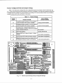
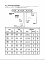
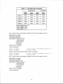
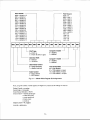
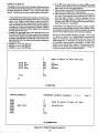
Factory-ConfiguredSwitch and Jumper Settings
Table 1-1 lists the factory settingsof the user-configurablejumpers and switches on the TC1024 board. Figure 1-1 shows the board layout and the locations of the factory-setjumpers. The following paragraphsexplain how
to changethe factory settings.Pay special attention to the setting of S1, the baseaddressswitch, to avoid address
contention when you first use your board in your system.
Table 1-1- FactorySettings
Switch/
Jumper
P5
Connectsthe outputof counter2 or 5 to an interrupt
channel(S4 selectswhichcounteris available)
P6
7 or 10to aninterrupt
Connects
theoutputof counter
Interruptchannelsdisabled
(S4selects
whichcounter
is available)
channel
P7
Connectsany of 11 interruptsourcesto any of 11
interruptchannels;connectionmadeby wirewrapping
No connection
betweenselectedheaderpins
S1
Setsthe baseaddress
300 hex (768decimal)
S2
Bypasses8255PortC buffersfor Mode1 or Mode2
operation
Open (buffersnot bypassed)
S3
Bypasses8255PortA buffersfor Mode2 operation
Open(buffersnot bypassed)
S4
Selectsthe interruptsourcesto be availableat P5 and
EXT6,EXT1
OUTs,OUT1O,
P6: selectsthe sourcefor counter1 andcounter6
sS€lOOi€$i
oo
XTAL
tro
FactorySettings
(JumpersInstalled)
FunctionControlled
Interruptchannelsdisabled
Sl S,t
i-A663-6;,3.ooooo@ooooooffi
oJ
rffi
ffiHHF
EF?4tsr44
(E666OO)*
I
Y/trOOOOOOOOO
6 utc
G;Dtr l.7]
ffiEffig
@Dq l--lo
ooo ooooooo
ffilalryoo
;A@*'*16,ffi
ref
@*1'i"_
Mod€inusA
(Eoooo.oooo\s"
o o o o o o o o o o o o o ooooo
)74HCr245
| )sa{rcH
I
trooooooooo trooooooo
q
ffiEffi3O
@Du lR6lo
leTOOOOOOOOOO
oooooo
oooooooo
G;Dtr I..FIO
Lgg
lBffi'ffi
lsEla.mffi
I
l6fu or-rr6ffol=@ssoEao
oooooooooo ooooo00000
FqL-l
llz+x4s-l
qooooooooo qooooooooo
u15
"'d@lc
+GiDor
/T\
Settings
Fig.1-1- BoardLayoutShowingFactory-Configured
1-3
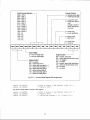
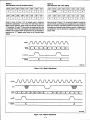
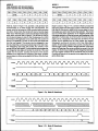
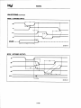
P5 -
Counter OUT 2i/5Interrupt Channel Select (Factory Setting: Interrupt Channels Disabled)
This headerconnector, shown in Figure l-2, lets you connect the output of counter 2 or 5, whichever is selected
on S4-1, to any of 11 intemrpt channels,IRQ9 (highest priority channel) through IRQl2, IRQ14, IRQ15, and then
back to IRQ3 through IRQT (lowest priority). Chapter 4 explains intemrpt channel prioritization in detail. To
activate a channel, you must install a jumper acrossthe desiredIRQ channel. Figure 1-2a shows the factory setting;
Figure 1-2b shows the intem.rpt sourceconnectedto IRQ3. If you use multiple intemrpts, make sure each sourceis
assignedto a different IRQ channel.
Fig.1-2a:
FactorySetting
IRQ 1514 12 11 10 I
Source
Fig.1-2b:Interrupt
Connectedto lRQg
P5
o aoooooaooH
R5
(rl
aooooaooaao
7 6 s 4 3
o oooooooooo?
u,RE o o o . o o o . o o l
rRo 1 5 1 4 1 2 1 1 1 0
P5
Fig. 1-2 - CounterOUT 215InterruptChannelSelectJumper, P5
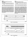
P6 - Counter OUT 7/l0Interrupt ChannelSelect(Factory Setting: Interrupt ChannelsDisabled)
This headerconnector,shownin Figure1-3,letsyou connecttheoutputof counter7 or 10,whicheveris
selectedon S4-2,to anyof 1l intemrptchannels,IRQ9 (highestpriority channel)throughIRQ12,IRQ14,IRQ15,
andthenbackto IRQ3 throughIRQT (lowestpriority).Chapter4 explainsinterruptchannelprioritizationin detail.
To activatea channel,you mustinstallajumperacrossthedesiredIRQ channel.Figure1-3ashowsthe factory
to IRQ9. If you usemultipleinterrupts,makesureeach
setting;Figure1-3bshowstheinterruptsourceconnected
sourceis assignedto a differentIRQ channel.
Fig.1-3a:
FactorySetting
o ooaoaoaaaH
{q
aoaaoooaooa
o
P6
IRQ 1 5 1 4 1 2 1 1 1 0
Source
Fig.1-3b:Interrupt
to lRQ9
Connected
o ooooo?ooooo
t5
o
I
oaoaooooooo
P6
tRo 1 5 1 4 12 1 1 1 0
Fig. 1-3 - CounterOUT 7/10 InterruptChannelSelectJumper,PO
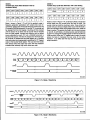
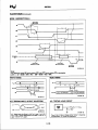
P7 - Interrupt Source/ChannelSelect(Factory Setting: No Connection)
This wire-wrapheaderconnector,shownin Figure1-4,letsyou connectanyof 11intemrptsourcesto anyof
pinson theheader.Designedto
the 11availableintemrptchannelsby wire-wrappingbetweenthe appropriate
providemaximumflexibility in interruptsourceselection,theinterruptsourcesprovidedare:PC3,which is the
INTRA signalfrom the 8255PPI;PCO,whichis theINTRB signalfrom the 8255PPI;EXT, an externalintemrpt
you canrouteontothe boardthroughtheP2 VO connector,andeightofthe 10counteroutputs(counters5 and 10
t-4
are not provided; however, they are available at P5 and P6). You can wire-wrap any sourceto any of 1i intenupt
channels,IRQg (highest priority channel) through IRQ12, IRQ14, IRQl5, and then back to IRQ3 through IRQT
(lowest priority). Chapter 4 explains intemrpt channel prioritization in detail. If you use multiple intemrpts, make
sure each source is assignedto a different IRQ channel.
OUT
!!m
o
(.o
) ox{
Fig. 1-4a:
Factory Setting
ooooooooooo
ooooooooooo
fRQls14 1211 1097
654
3
ouT
!!m
g)o{
oox
Fig.1-4b:EXTConnected
tolRQ11
P7
oo\oooooooo
o o ob o o o o o o o
P7
IRQ 15 14 1211 10
Fig. 1-4 -
51-
lnterruptSource/ChannelSelectWire-WrapHeader,P7
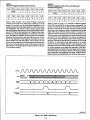
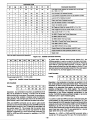
BaseAddress(Factory Setting:300 hex (768decimal))
Oneof the mostcommoncausesof failurewhenyou arefirst trying your boardis addresscontention.Someof
WhentheTC1024board
your computer'sVO spaceis alreadyoccupiedby internalVO andotherperipherals.
attemptsto useVO addresslocationsalreadyusedby anotherdevice,contentionresultsandtheboarddoesnot work.
DIP switch,Sl, whichletsyou selectany oneof 32
To avoidthis problem,theTClO24hasan easilyaccessible
in thecomputer'sVO. Shouldthefactorysettingof 300hex (768decimal)be unsuitablefor your
startingaddresses
system,you canselecta differentbaseaddresssimplyby settingthe switchesto anyvalueshownin Table l-2.The
(in parentheses)
values.Make sure
decimalandhexadecimal
tableshowsthe switchsettingsandtheircorresponding
thatyou verify the orderof the switchnumberson the switch(l through5) beforesettingthem.Whenthe switches
arepulledforward,theyareOPEN,or setto logic 1, aslabeledon theDIP switchpackage.Whenyou setthebase
addressfor your board,recordthe valuein thetableinsidethebackcover.Figure1-5showstheDIP switchsetfor a
baseaddressof 300 hex (768decimal).
Fig.1-5- BaseAddressSwitch,51
t-5
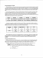
Table1-2- BaseAddressSwitchSettings,51
BaseAddress
Decimal/ (Hex)
BaseAddress
Decimal/ (Hex)
SwitchSetting
54321
SwitchSetting
54321
sr2| (200)
00000
768/ (300)
10000
s28I (210)
00001
784| (3r0)
10001
544| (220)
00010
10010
s6o| (230)
00011
800tQza)
816/ (330)
s76| (240)
00100
832| (340)
10100
592| (2s0)
00101
848/ (350)
10101
608/ (260)
00110
864/ (360)
10110
6',24
| (270)
00111
880/ (370)
10111
640| (280)
01000
896/ (380)
11000
6s6| (290)
01001
9r2| (390)
11001
672| (240)
01010
928/ (3A0)
tl0l0
688/ (2B0)
01011
944| (380)
r1011
704| (2CO)
01100
960/ (3C0)
1100
720| (2D0)
01101
976| (3D0)
ll01
736| (2E0)
01110
992| (380)
11110
01111
1008/ (3F0)
11111
7s2t (2FO)
10011
0 = c l o s e d 1, = o P € n
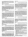
52 and 53 -
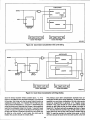
Buffer Bypass Switches (Factory Setting: OPEN (Not Bypassed))
Mode 1 Operation (S2) - When operating the 8255 in Mode 1, the lines of Port C function as control lines,
some as outputs and some as inputs. When using Mode 1, the Port C buffers must be removed and bypassedto allow
the Port C lines to be individually set as inputs or outputs. Figure 1-6 shows the Port C buffers, and the following
stepstell you how to configure the board for Mode 1 operation.
To remove buffering from Port C:
1. Close DIP switches 1 through 8 on 52.
2. Remove U10 from the board.
3. Remove U11 from the board.
CAUTION: Remember, whenever you close the switches on 52, be sure to remove the Port C buffers, U10
and U11, from the board. Failure to do so may damagethe board.
Mode 2 Operation (S2, 53) - When operating the 8255 in Mode 2, the lines of Port A must be bidirectional
and the lines of Port C function as control lines, some as outputs and some as inputs. When using Mode 2, both the
Port A and Port C buffers must be removed and bypassed.Figure 1-7 shows the Port A buffers, Figure 1-6 shows the
Port C buffers, and the following stepstell you how to configure the board for Mode 2 operation.
To remove buffering from Ports A and C:
tr.
2.
3.
4.
5.
Close DIP switches I through 8 on 53 @ort A).
Remove U8 from the board.
Close DIP switches 1 through 8 on 52 (Port C).
Remove U10 from the board.
Remove Ul l from the board.
1-6
1024
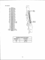
UO CONNECTOR
P4IP3
I
PC7
PC6
PC5
PC4
PIN35
PIN36
PIN37
PC1
PIN38
Fig.1-6- PortC BufferCircuitry
1024
I/O CONNECTOR
P4
Fig.1-7- PortA BufferCircuitry
CAUTION: Remember, whenever you close the switches on 52 and 53, be sure to remove the buffers, U8,
U10, and Ul1, from the board. Failure to do so may damagethe board.
54 -
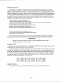
Interrupt Source/Clock Source Select (Factory Setting: OUT5, OUT10' EXT6, EXTI)
These four single-pole, double-throw switches, shown in Figure 1-8, let you select which counter output
provides the intemrpt source for P5 and P6, and let you selectthe clock sourcefor counters 1 and 6.
S4-1. This switch provides the output of counter 5 or the output of counter 2 as the available intemrpt source at
P5. The factory setting is OUT5. Figure 1-9 shows how this switch is connected,
S4-2. This switch provides the output of counter 10 or the output of counter 7 as the available intemrpt source
at P6. The factory setting is OUT10. Figure 1-9 shows how this switch is connected.
S4-3. This switch controls the clock sourcefor counter 6. The sourcecan be provided externally from the P3
VO connector, or it can be provided from the output of counter 5, cascadingcounter 6 to counter 5. The factory
setting is external, EXT6 (SRC 6 at the I/O connector).Figure 1-9 shows how this switch is connected.
S4-4. This switch controls the clock sourcefor counter l. The sourcecan be provided externally from the P3
VO connector, or it can be provided from the output ofcounter 10, looping counter l0's output back around to
counter 1. The factory setting is external, EXTI (SRC 1 at the VO connector).Figure 1-9 shows how this switch is
connected.
S4
OUT2 OUTT OUTSOUT1O
1
2
3
4
EEEE
OUTsOUT1OEXT6 EXT1
SourceSelectSPDTSwitch,54
Source/Clock
Fig.1-8- Interrupt
t-8
1024
I/O CONNECTOR
P3
I
COUNTER
I
1 lsHc
cLK
OUT I
OUT
COUNTER
2
I
PrN7 | SRC
cLK
GATE
2
OUT
COUNTEF
3
3
CLK
GATE
nl
OUT
COUNTER
4
CLK
GATE
GATE
OUT
COUNTER
5
CLK
loerr
OUT
I
I
I
I
s4-l
i-,
A M 9 5 1 3f 2 - U 3
COUNTER
6
I
TO P5
IRQ HEADER
I
I
s4-3
ls"c
CLK
o)
GATE
OUT
COUNTER
z
I
I
P I N8 r S R C7
CLK
7
lort
OUT
COUNTER
8
7
R
CLK
GATE
8
OUT
COUNTER
9
o
CLK
:9
GATE
o
OUT
COUNTER
10
10
CLK
:10
10
OUT
I
s4-2
TO P6
IRQ HEADER
Fig.1-9- CounterCircuitry
54 SwitchConnections
Showing
1-9
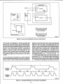
Pull-up/Pull-down Resistorson Digital UO Lines
The 8255 programmable peripheral interface provides 24TTLICMOS compatible digital VO lines which can be
interfaced with external devices. The lines are divided into four groups: eight Port A lines, four Port C Lower lines,
eight Port B lines, and four Port C Upper lines. You can install and connectpull-up or pull-down resistors for any or
all of these four groups of lines. You may want to pull lines up for connection to switches.This will pull the line
high when the switch is disconnected.Or, you may want to pull down lines connectedto relays which control
turning motors on and off. Thesemotors turn on when the digital lines controlling them are high. The Port A and
Port B lines of the 8255 automatically power up as inputs - which can float high - during the few moments before
the board is initialized. This can causeexternal devices connectedto these lines to operateerratically. By pulling
these lines down, when the data acquisition system is first turned on, the motors will not switch on before the 8255
is initialized.
To use the pull-up/pull-down feature, you must first install resistor packs in any or all of the four locations
around the 8255, labeled PA, PB, PCL, and PCH. PA and PB take 10-pin packs, and PCL and PCH take 6-pin
packs. Figure 1-10 shows a blowup of this circuitry.
ooooooo
74HCf245
o
gEEs
tGHor:@
oooooooooo
5?lHsrrrs
I
trooooooooo
Circuitry
Fig.1-10- Pull-up/Pull-down
Resistor
t-10
After the resistor packs are installed, you must connect them into the circuit as pull-ups or pull-downs. Locate
the three-hole pads on the board near the resistor packs. They are labeled G (for ground) on one end and V (for +5V)
on the other end. The middle hole is common. PA is for Port A, PB for Port B, PCL is for Port C Lower, and PCH is
for Port C Upper. Figure 1-10 shows a blowup of the pads. To operateas pull-ups, solder a jumper wire between the
common pin (middle pin of the three) and the V pin. For pull-downs, solder a jumper wire between the common pin
(middle pin) and the G pin. Figure 1-11 shows Port A lines with pull-ups, Port C Lower with pull-downs, and Port C
Upper with no resistors.
8255
(
,o^, o )
(PA0-7)
\
I
,o^,
LOWER
" <f
(rc0-3)
[
to SomeDigitall/O Lines
andPull-downs
Fig.1-11- AddingPull-ups
1-1I
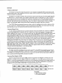
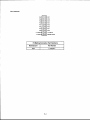
RC Filters on SourceClock Input Lines
On-board pads are provided to add custom filtering on each ofthe 10 sourceclock input lines. These RC pads,
located in the upper right areaof the board, let you build a switch debouncingcircuit or a circuit to eliminate
uwanted ringing on the clock input. Simply calculate the values you want to use to achieve the desiredresults and
solder the componentsonto the board. Figure 1-12 shows a switch debouncingcircuit for the TCLOZ4source clock
inputs. Table 1-3 lists the resistor-capacitorpairs for each sourceclock input line.
TO AM9513A
S O U R C EI N P U T
F = 1 +2nRC
F=1 +2n(100)(1OpF)
F=159H2
T'o
V
FilterCircuit
Fig.1-12- TypicalSwitchDebouncing
Table1-3- SourceClock RC Filters
SourceClock
Number
Resistor
Number
Capacitor
Number
1
R2
c20
2
R3
3
R4
c21
c22
4
R5
5
R6
c23
c24
6
R7
c25
7
R8
I
R9
c26
c27
9
R10
10
R11
t-t2
c28
c29
CHAPTER 2
BOARD INSTALLATION
The TC1024 is easyto install in your PC/AT or compatible
computer. This chaptertells you step-by-stephow to install and
connect the board.
After you have installed the board and made all of your connections,you can turn your systemon and run the 1024DIAG
board diagnosticsprogram included on your example software disk
to verify that your board is working.
2-l
Board Installation
Keep the board in its antistatic bag until you are ready to install it in your computer. When removing it from the
bag, hold the board at the edgesand do not touch the componentsor connectors.
Before installing the board in your computer, check the jumper and switch settings.Chapter 1 reviews the
factory settings and how to changethem. Ifyou need to changeany settings,refer to the appropriateinstructions in
Chapter 1. Note that incompatible jumper settingscan result in unpredictableboard operation and erratic response.
To install the board:
1. Turn OFF the power to your AT computer.
2. Remove the top cover of the computer housing (refer to your owner's manual if you do not already know
how to do this).
3. Select any unusedexpansionslot and remove the slot bracket.
4. Touch the metal housing of the computer to dischargeany static buildup and then remove the board from its
antistatic bag.
5. If you are using the 20-pin P4 connector for 8255 digital VO operations,connect the mating connector to it
before installing the board in the PC. Note that the P3 VO connectormounting bracket has an oversized
cutout to allow spacefor running the cable to P4 through the sameI/O slot. If you want to run both cables
through the same slot, you must make theseconnectionsbefore installing the board.
6. Holding the board by its edges,orient it so that its card edge (bus) connectorsline up with the expansionslot
connectorsin the bottom of the selectedexpansionslot.
7 . After carefully positioning the board in the expansionslot so that the card edge connectorsare resting on the
computer's bus connectors,gently and evenly pressdown on the board until it is securedin the slot.
NOTE: Do not force the board into the slot. If the board does not slide into place, remove it and try again.
Wiggling the board or exerting too much pressurecan result in damageto the board or to the computer.
8. After the board is installed, securethe slot bracket back into place and put the cover back on your computer.
The board is now ready to be connectedvia the external VO connector at the rear panel of your computer. Be
sure to observe the keying when connecting your external cable to VO connectorP3.
External VO Connections
Figure 2-1 shows the TC1024's P3 50-pin VO connectorand P4 on-board 20-pin connector pinouts. Refer to
these diagrams as you make your VO connections.
z-J
sRc6
sRcl
GATEl
GATE6
OUTl
ouT6
sRc2
sRcT
GATE2
GATET
OUT2
OUTT
sBc3
sRc8
GATE3
GATES
OUT3
OUTS
sRc4
sRc9
GATE4
ouT4
sRcS
GATE5
OUT5
GATE9
OUTg
sRc10
GATEIO
ouTl0
EXTINT
DIGITALGND
FOUT
DIGITAL GND
PA7
PC7
PC3
PC2
PA6
PC6
PCI
PC0
PA5
Pc5
P87
PB6
PA4
PC4
PB5
P84
PA3
PC3
PB3
PB.2
PA2
PC2
PA1
PCt
PAO
PC0
PBI
+12 VOLTS
-12 voLTs
Fig. 2-1 -
P3
50-Pin
PBO
+5 VOLTS
+12 VOLTS
-12VOLTS
DIGITAL GND
P4
2o-Pin
+5 VOLTS
DIGITALGND
P3 l/O Connector and P4 On-board Connector Pin Assignments
Connecting the Timer/Counters and Digital UO
For all of these connections,the high side of an external signal sourceor destination device is connectedto the
appropriatesignal pin on the P3 VO connector or on P4, and the low side is connectedto any DIGITAL GND.
Running the [024DIAG DiagnosticsProgram
Now that your board is ready to use, you will want to try it out. An easy-to-use,menu-driven diagnostics
program, 1024DIAG, is included with your example software to help you verify your board's operation. You can
also use this program to make sure that your current baseaddresssetting does not contend with anotherdevice.
2-4
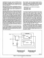
CHAPTER 3
HARDWARE DESCRIPTION
This chapterdescribesthefeaturesof theTCt024 hardware.
andthe digital VO lines.
The majorcircuitsarethe timer/counters
intemrpts.
This chapteralsodescribesthe hardware-selectable
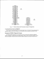
andthedigitalVO lines.Figure3-1 showsthe
The TC1024boardhastwo majorcircuits,the timer/counters
thehardwarewhichmakesup themajorcircuitsandhardwareblock diagramof the board.This chapterdescribes
interrupts.
selectable
Fig.3-1-TC1024BlockDiagram
Am9513A Timer/Counters
The Am9513A System Timing Controller contains five generalpurpose l6-bit timer/counters which are capable
performing
many different types of counting, sequencing,and timing functions. The Am9513A supports up or
of
down counting in binary or BCD with hardware or software gating of each counter. Its 24 modes of operation are
detailed in the Am95l3AData Sheetreprint from AMD included in Appendix C.
The Am95 13A is structured with a seriesof internal registersthat set the mode of operation for each counter.
These registers are fully describedin Appendix C.
Any combination of the 10 countersin the two Am9513As can be internally cascadedto createa counter of up
to 160 bits. For example, two cascadedcountersform a 32-bit counter for longer counting capability. Rarely is it
practical to cascademore than three counters.Cascadingis describedin Appendix C, Chapter 3 of the Am9513A
data sheet.
The timer/counters are driven by an on-board 5 MHz crystal oscillator. On-board RC pads let you custom filter
each source clock input line for switch debouncingand elimination of unwanted ringing.
Digital VO, Programmable Peripheral Interface
The 8255 programmable peripheral interface (PPI) can be easily configured to solve a wide range of digital
real-world problems. This high-perfornance TIL/CMOS compatible chip has 24 parallel programmable digital VO
lines divided into two groups of 12lines each:
Group A Group B -
Port A (8 lines) and Port C Upper (4 lines);
Port B (8 lines) and Port C Lower (4 lines).
3-3
Each group can be programmed for one of three modes of operation. When operating in Mode l, the on-board
buffers must be removed from the Port C lines. When operating in Mode 2, both Port A and Port C buffering must
be removed. This procedure is describedin Chapter I in the 52 and 53 DIP switch discussion.The three operating
modes are:
Mode 0 - Basic input/output. Lets you use simple input and output operation for a port. Data is written to or
read from the specified port.
Mode 1 - Strobed input/output. Lets you transfer VO data from Port A in conjunction with strobesor handshaking signals.
Mode 2 - Strobed bidirectional inpuVoutput. Lets you communicatebidirectionally with an external device
through Port A. Handshakingis similar to Mode l.
These modes are detailed in the 8255 Data Sheet,reprinted from Intel in Appendix C.
The bidirectional buffers on the 8255's I/O lines monitor the 8255 control word to automatically set their
direction. Hardware changesto the buffer circuitry are required only when using Mode I or Mode 2, where the Port
A and/or Port C buffers must be removed as describedin Chapter l.
Interrupts
The TC1024 has severalhardware selectableintemrpt sources.These intemrpt sourcescan be selectedusing
jumpers or wire-wrapping on P5 through P7, as describedin Chapter 1. Interrupt sourceswhich can be used by the
TCI024 are: the outputs from all 10 Am9513A counters;PC3, which is the INTRA signal from the 8255 PPI; PC0,
which is the INTRB signal from the 8255 PPI; and EXT, an external intemrpt you can route onto the board through
VO connector P3. Chapter 1 tells you how to set the jumpers or configure the wire-wrapping on the interrupt header
connectors,P5, P6, andP7, and Chapter 4 describeshow to program intemrpts.
3-4
CHAPTER 4
BOARD OPERATION AND PROGRAMMING
This chaptershowsyou how to programyour TClO24boudby
writing to andreadingfrom the AT busin 8- or 16-bitwords.It
providesa completedescriptionof the VO mapanda description
of programmingoperationsto aid you in programming.The
exampleprogramsincludedon thedisk in your boardpackageare
listedat the endof this chapter.Theseprograms,writtenin Turbo
C andTurboPascal,includesourcecodeto simplify your
applicationsprogramming.Chapter5 containsexamplesfor setting
up theAm9513A.'s16-bitcountersfor specificapplications.
4-1
4-2
Defining the UO Map
The VO map for the TC1024 is shown in Table 4-1 below. As shown, the board occupies 16 consecutiveVO
port locations.
Becauseof the 16-bit structure of the AT bus, every other addresslocation is used, even for 8-bit transfers.Our
programming structure usesthe l6-bit command to set up and run the Am9513A. All 8255 read/write operationsare
8-bit operations.
The baseaddress(designatedas BA) can be selectedusing DIP switch Sl as describedin Chapter l, Board
Settings.This switch can be accessedwithout removing the board from the computer. 51 is factory set at 300 hex
(768 decimal). The following sectionsdescribethe register contentsof each addressused in the VO map.
Table 4-1- TC1024UO Map
8255PPIPortB
Address *
(Decimal)
Write
Function
ReadFunction
ProgramPortA digitaloutput
BA+0
ReadPortA digitalinputlines lines
PortB digitaloutput
Program
BA+2
Read Port B digitalinput lines lines
8255PPIPortC
Read Port C digitalinput lines lines
8255PPIControlWord
Reserued
Am9513A#1 Data Word
Read data registerfor
Counters1-5
RegisterDescription
8255PPIPortA
ProgramPortC digitaloutput
ProgramPPIconfiguration
Programdataregisterfor
1-5
Counters
for
Readcontrolregister
1-5
Counters
Am9513A#1 ControlWord
for
Readdataregister
6-10
Am9513A#2 DataWord Counters
for
Readcontrolregister
6-10
#2 ControlWordCounters
Am9513A
* BA = BaseAddress
Programcontrolregisterfor
Counters1-5
Programdataregisterfor
Counters
6-10
Programcontrolregisterfor
6-10
Counters
BA+4
BA+6
BA+8
BA+10
BA+12
BA+14
BA + 0: PPI Port A - Digital I/O (Read/Write)
8-bit operation. Transfersthe 8-bit PortA digital inputanddigitaloutputdatabetweentheboardandan
externaldevice.A readtransfersdatafrom the externaldevice,throughon-boardconnectorP4, andinto PPI Port A;
a write transfersthe written datafrom Port A throughP4 to an externaldevice.
BA + 2: PPI Port B - Digital VO (Read/Write)
8-bit operation. Transfersthe 8-bitPortB digital inputanddigitaloutputdatabetweentheboardandan
externaldevice.A readtransfersdatafrom theexternaldevice,throughexternalVO connectorP3,andinto PPI Port
B; a write transfersthe writtendatafrom PortB throughP3 to an externaldevice.
B.d + 4: FPI Port C - Digital VO (Read/Write)
8-bit operation. Transfersthe two 4-bit PortC digitalinput anddigital outputdatagroups(PortC Upperand
PortC Lower) betweentheboardandan externaldevice.A readtransfersdatafrom theexternaldevice,throughonboardconnectorP4, andinto PPI PortC; a write transfersthewrittendatafrom PortC throughP4 to an external
device.The bottomfour bits,PC0-PC3,arealsobroughtout to externalVO connectorP3.
4-3
BA + 6: 8255 PPI Control Word (Write Only)
8-bit operation. When bit 7 of this word is set to 1, a write programs the PPI configuration. The table below
shows the control words for the 16 possible Mode 0 Port VO combinations.
D7
D5
D6
D3
D4
D1
-l rr--l--T.
r
ModeSet Fns
i
1 = active
1",
rde Seler:t
= mode
= mode
t c= mode
I
I
I
I
ll
lt
|
|
It
I
iilll=i
i3:
I
D2
Port A
0 = output
1 = input
l1
li
t;l
-l
P otr C
t Lower
0 = output
c
input
eorte
o=output
1=inPut
1 | Mode Select
il o=modeo
:l
I
Port G Upper
0=output I
I
|
|
|
|
DO
1=mode1
L
i3!-B-l
fr""f___,=,"0r,__l
8255Port l/O Flow Directionand ControlWords,Mode0
ControlWord
GroupB
GroupA
Port A
Port C
Upper
Port B
Port C
Lower
Binary
Decimal
Hex
Output
Output
Output
Output
10000000
128
80
Output
Output
Output
Input
10000001
129
81
Output
Output
Input
Output
10000010
130
82
Output
Output
Input
Input
10000011
131
83
Output
lnput
Output
Output
10001000
136
88
Output
Input
Output
Input
10001001
137
89
Output
Input
Input
Output
10001010
138
8A
Outpul
Input
Input
Input
100010'l 1
139
8B
Input
Output
Output
Output
10010000
144
90
Input
Output
Output
Input
10010001
145
91
Input
Output
Input
Output
10010010
92
Inpul
Output
Input
Input
10010011
146
't47
Input
lnput
Output
Output
10011000
152
98
Inpul
Input
Output
Input
10011001
153
99
Input
Input
Input
Output
10011010
'154
9A
Input
Input
Input
Input
10011011
155
9B
4-4
93
bit 7 of this word is set to 0, a write can be usedto individually program the Port C lines.
D7
D5
D6
D4
D2
D3
SeUReset
FunctionBit
0 = active
D1
DO
Bit SeUReset
0=setbitto0
1=setbittol
Bit Select
ggg= pCO
001= PC1
010= PC2
0 1 1= P C 3
100= PC4
101= PCS
1 1 0= P C 6
1 1 1= P C 7
For example, if you want to set Port C bit 0 to 1, you would set up the control word so that bit 7 is 0; bits 1, 2,
and 3 are 0 (this selectsPC0); and bit 0 is 1 (this setsPCOto 1). The control word is set up like this:
0xxxo001
Sets PCOto 1:
(writtento BA +6)
D7
SeUReset
FunctionBir
D6
D5
D2
D3
D4
X = don't care
D1
DO
Set PGO
Bit Select
000= PCO
IMPORTANT
Becauseof the bus releasetime of the Am95l3A, AMD recommendsyou insert a small
delay between software accessesto the chip.
BA + 8: Am9513A #l Data Register (Read/Write)
16-bit operation (after initialization). Accessesthe Am9513A data register for counters 1-5. This chapter
explains initialization procedures.Seethe example programs in Chapter 5 and the data sheetincluded in Appendix C
for more information on the operation of the Am9513A.
BA + 10: Am9513A #L Command Register (Read/Write)
L6-bit operation (after initialization). Accessesthe Am9513A command register for counters 1-5. This
chapter explains initialization procedures.See the example programs in Chapter 5 and the data sheetincluded in
Appendix C for more information on the operation of the Am9513A.
BA + 12: Am9513A #2Data Register (Read/Write)
16-bit operation (after initialization). Accessesthe Am9513A data register for counters6-10. This chapter
explains initialization procedures.Seethe example programs in Chapter 5 and the data sheetincluded in Appendix C
for more information on the operation of the Am9513A.
BA + 14: Am9513A #2 Command Register (Read/Write)
16-bit operation (after initialization). Accessesthe Am9513A command register for counters 6-10. This
chapter explains initialization procedures.Seethe example programs in Chapter 5 and the data sheetincluded in
Appendix C for more information on the operation of the Am9513A.
4-5
Programming the TCLO?
This section gives you some generalinformation about programming and theTCl024 board. Chapter 5 provides
some specific programming examples,and the Am95l3A data sheetin Appendix C provides detailed programming
information for all24 operating modes of the Am95l3A. These tools will help you as you use the example programs
included with the board. All of the program descriptionsin this section use decimal values unlessotherwise specified"
The TCl024 is programmed by writing to and reading from the correct UO port locations on the board. These
VO ports were defined in the previous section. BecausetheTCl024 is AT bus compatible, reading/writing the
Am9513As is done in a 16-bit word format. All other operationsare done in an 8-bit word format. HighJevel
languagessuch as Pascal,C, and C++ make it very easy to readlwite theseports. The table below shows you how to
read from and write to VO ports in Turbo C and Turbo Pascal.
Language
Read8 Bits
Write8 Bits
Read
16Bits
Write16Bits
Data)
Data) Data= inport(Address)outport(Address,
outportb(Address,
Data= inportb(Address)
TurboC
:=Data
Port[Address]Port[Address]
TurboPascal Data:=
Data
Data:=PortW[Address]PortW[Address]:=
In addition to being able to read/write the VO ports on theTClO24, you must be able to perform a variety of
operationsthat you might not normally use in your programming. The table below shows you some of the operators
discussedin this section, with an example of how each is used with Pascaland C.
Language
c
Modulus
IntegerDivision
o/
/o
a=b7oc
Pascal
MOD
a : = b M O Dc
a=blc
DIV
a:=bDlVc
AND
&
a=b&c
AND
a:=bANDc
OR
I
a=blc
OR
a:=bORc
Many compilers have functions that can read/write either 8 or 16 bits from/to an VO port. For example, Turbo
PascalusesPort for 8-bit port operationsand PortW for 16 bits, Turbo C usesinportb for an 8-bit read of a port
and inport for a 16-bit read. Be sure to use the correct function for 8-bit and 16-bit operations with the
TCIO2A'!
Clearing and Setting Bits in a Port
When you clear or set one or more bits in a port, you must be careful that you do not changethe statusof the
other bits. You can preservethe statusof all bits you do not wish to changeby proper use of the AND and OR
binary operators.Using AND and OR, single or multiple bits can be easily clearedin one operation.
To clear a single bit in a port, AND the current value of the port with the value b, where b = 255 - Zbit.
Example: Clear bit 5 in a port. Read in the current value of the port, AND it with 223
(223 =255 - 2s),and then write the resulting value to the port. In BASIC, this is programmed as:
V - INP(PortAddress)
V=VAND223
V
OUT PortAddress,
4-6
To set a single bit in a port, OR the current value of the port with the value b, where b = 2b7.
Example: Set bit 3 in a port. Read in the current value of the port, OR it with 8 (8 = 23),and then
write the resulting value to the port. In Pascal,this is programmed as:
V := Port IPortAddress];
V := V OR 8;
:= V;
PorLIPortAddress]
Setting or clearing more than one bit at a time is accomplishedjust as easily. To clear multiple bits in a port,
AND the current value of the port with the value b, where b = 255 - (the sum of the values of the bits to be cleared).
Note that the bits do not have to be consecutive.
Example: Clear bits 2,4, and 6 in a port. Read in the current value of the port, AND it with 171
(l7I =255 - 22 - 2o- 2u),and then write the resulting value to the port. In C, this is programmed
AS:
v = inportb(port-address)
v=v&t1L;
outportb (port-address,
;
v) ;
To set multiple bits in a port, OR the current value of the port with the value b, where b = the sum of the
individual bits to be set. Note that the bits to be set do not have to be consecutive.
Example: Set bits 3, 5, and 7 in a port. Read in the current value of the port, OR it with 168
(168 = 23 + 25 + 21), and then write the resulting value back to the port. In assemblylanguage,this
is programmed as:
mov dx, PortAddress
in al, dx
or al, 168
out dx, al
Often, assigning a range of bits is a mixture of setting and clearing operations.You can set or clear each bit
individually or use a faster method of first clearing all the bits in the range then setting only those bits that must be
set using the method shown above for setting multiple bits in a port. The following example shows how this twostep operation is done.
Example: Assign bits 3, 4, and 5 in a port to 101 (bits 3 and 5 set, bit 4 cleared).First, read in the
port and clear bits 3,4, and 5 by ANDing them with 199. Then set bits 3 and 5 by ORing them
with 40, and finally write the resulting value back to the port. In C, this is programmed as:
v = inportb(port_address),v-v&199;
v = v | 40;
v) ;
outportb (port-address,
A final note: Don't be intimidated by the binary operatorsAND and OR and try to use operatorsfor which you
have a better intuition. For instance,ifyou are tempted to use addition and subtraction to set and clear bits in place
of the methods shown above, DON'T! Addition and subtractionmay seemlogical, but they will not work if you try
to clear a bit that is already clear or set a bit that is already set. For example, you might think that to set bit 5 ofa
port, you simply need to read in the port, add 32 (25)to that value, and then write the resulting value back to the port.
This works fine if bit 5 is not already set. But, what happenswhen bit 5 is already set?Bits 0 to 4 will be unaffected
and we can't say for sure what happensto bits 6 and 7, but we can say for sure that bit 5 ends up cleared instead of
being set. A similar problem happenswhen you use subtractionto clear a bit in place of the method shown above.
Now that you know how to clear and set bits, we are ready to look at the programming stepsfor the TCl024
board functions.
4-7
Initializing the Am9513A
The Am9513A has a sophisticatedinternal architecturewhich is programmed through a seriesof internal
registers.These internal registers are accessedby writing to and reading from only two VO port locations for each
Am9513A. on the TC1024 board. For Am9513A #1 which contains counters 1-5, the Data Register port is at BA + 8
and the Control Register port is at BA + 10. For Am9513A #2 which contains counters 6-10, the Data Register port
is at BA + 12 and the Control Register port is at BA + 14. In our example programs, follow these stepsto initialize
the Am9513A. Note that until you point to and set up the master mode register in step 2, you must send your
commands in S-bit format. After the master mode register has been configured for 16-bit operation by setting bit 13
to a logic 1, you can then send 16-bit words to the Am9513A.
1. Senda masterresetto the Am9513A (8-bit)
2. Point to and set up the master mode register (8-bit)
(When setting up the master mode register, set MM13 to logic I so that you can do 16-bit transfers)
3. Point to and set up counter 1 mode register (16-bit)
4. Point to counter 1 load register and load desiredvalue (16-bit)
5. Point to and set up counter 2mode register (16-bit)
6. Point to counter 2 load register and load desiredvalue (16-bit)
a
11. Point to and set up counter 5 mode register (16-bit)
12. Point to counter 5 load register and load desiredvalue (16-bit)
13. Load and arm counters (16-bit)
The examples on the disk and in Chapter 5 will aid you in programming the Am9513A for your application.
These tools and the data sheetin Appendix C provide a comprehensivedescription of timer/counter operation.
IMPORTANT
Becauseof the bus releasetime of the Am95 13A, AMD recommendsyou insert a small
delay between software accessesto the chip.
Initializing the 8255
Before you can use the 24 digital VO lines on your TC|OT4, the 8255 PPI must be initialized. This step must be
executedevery time you start up, reset,or reboot your computer.
The 8255 is initialized by writing the appropriatecontrol word to VO port BA + 6. The contents of your control
word will vary, depending on how you want to configure your VO lines. Use the control word description in the
previous VO map section to help you program the right value. In the example below, a decimal value of 128 setsup
the 8255 so that all VO lines are Mode 0 outputs. Rememberthat if you want to use Mode I or Mode 2 operation,
you must remove the Port A and/or Port C buffers from the board and close the buffer bypass switches.Chapter I
explains how to do this in the paragraphscovering 52 and 53.
D7
D6
D5
D4
D3
D2
D1
DO
Digital VO Operations
Oncethe 8255is initialized,you canusethedigitalVO linesto controlor monitorexternaldevices.
4-8
Interrupts
. What Is an Interrupt?
An interrupt is an event that causesthe processorin your computer to temporarily halt its current processand
execute another routine. Upon completion of the new routine, control is returned to the original routine at the point
where its execution was intemrpted.
Interrupts are very handy for dealing with asynchronousevents (eventsthat occur at less than regular intervals).
Keyboard activity is a good example; your computer cannot predict when you might press a key and it would be a
waste of processortime for it to do nothing while waiting for a keystroke to occur. Thus, the interrupt schemeis
'intemrpts' the
used and the processorproceedswith other tasks. Then, when a keystroke does occur, the keyboard
processor,and the processorgets the keyboard data, placesit in memory, and then returns to what it was doing
before it was intemrpted. Other cornmon devicesthat use intemrpts are modems,disk drives, and mice.
Your TCl024 board can interrupt the processorwhen a variety of conditions are met, such as when any of the
10 timer countdowns is finished. Intemrpts can also be generatedby the 8255 PPI or an external source.By using
these interrupts, you can write software that effectively deals with real world events.
. Interrupt Request Lines
To allow different peripheral devices to generateinterrupts on the samecomputer, the AT bus has 16 different
interrupt request (IRQ) lines. A transition from low to high on one ofthese lines generatesan interrupt request
which is handled by one of the AT's two intemrpt control chips. One chip handlesIRQO through IRQT and the other
chip handles IRQ8 through IRQl5. The controller which handlesIRQ8-IRQl5 is chained to the first controller
through the IRQ2 line. When an IRQ line is brought high, the interrupt controllers check to seeif intemrpts are to be
acknowledged from that IRQ and, if anotherinterrupt is already in progress,they decide if the new request should
supersedethe one in progressor if it has to wait until the one in progressis done. This prioritizing allows an
interrupt to be intemrpted if the secondrequesthas a higher priority. The priority level is determined by the number
of the IRQ. Becauseof the configuration of the two controllers, with one chained to the other through IRQ2, the
priority schemeis a little unusual. IRQO has the highest priority, IRQ1 is second-highest,then priority jumps to
IRQ8, IRQ9, IRQ10, IRQl1, IRQ12, IRQ13, IRQ14, and IRQ15, and then following IRQ15, it jumps back to IRQ3,
IRQ4, IRQ5, IRQ6, and finally, the lowest priority, IRQ7. This sequencemakes senseif you consider that the
controller that handles IRQS-IRQIS is routed through IRQ2.
. 8259 Programmable Interrupt Controllers
The chips responsiblefor handling interrupt requestsin the PC are the 8259 ProgrammableInterrupt Controllers. The 8259 thathandles IRQ0-IRQ7 is referred to as 8259A, and the 8259 that handlesIRQ8-IRQl5 is referred
to as 8259B. To use intemrpts, you need to know how to read and set the 8259 intemrpt mask registers (IMR) and
how to send the end-of-intemrpt (EOI) command to the 8259s.
.Interrupt
Mask Registers (IMR)
Each bit in the interrupt mask register (IMR) contains the mask statusof an IRQ line; in 8259A, bit 0 is for
IRQ0, bit 1 is for IRQI, and so on, while in 8259B, bit 0 is for IRQ8, bit I is for IRQ9, and so on. If a bit is set
(equal to 1), then the correspondingIRQ is masked and it will not generatean interrupt. If a bit is clear (equal to 0),
then the correspondingIRQ is unmaskedand can generateinterrupts. The IMR for IRQO-IRQ7 is programmed
through portzlH, and the IMR for IRQS-IRQIS is programmed through port AlH.
IRQT
tRo6
IRQs
IRQ4
IRQ3
IRQ2
rR o l 5 rRo14 rR o l 3 IRQ12 I R Q 1 1 I R Q l O
tRol
tRoo
l/O Port21H
IRQ9
IRQS
l/O PortA1H
For all bits:
(enabled)
0 = IRQunmasked
1 = IRQmasked(disabled)
4-9
. End-of-Interrupt
(EOI) Command
After an intemrpt service routine is complete, the appropriate 8259 intemrpt controller must be notified. When
using IRQO-IRQ7, this is done by writing the value 20H to I/O port 20H only; when using IRQ8-IRQl5, you must
write the value 20H to VO ports 20H and A0H.
. What Exactly Happens When an Interrupt Occurs?
Understanding the sequenceof events when an interrupt is triggered is necessaryto properly write software
intemrpt handlers.When an interrupt requestline is driven high by a peripheral device (such as the TC1024), the
intemrpt controllers check to seeif intemrpts are enabledfor that IRQ, and then check to seeif other intemrpts are
active or requestedand determine which intemrpt has priority. The intemrpt controllers then intemrpt the processor.
The current code segment(CS), instruction pointer (IP), and flags are pushedon the stack for storage,and a new CS
and IP are loaded from a table that exists in the lowest 1024 bytes of memory. This table is referred to as the
interrupt vector table and each entry is called an intemrpt vector. Once the new CS and IP are loaded from the
intemrpt vector table, the processorbegins executing the code located at CS:IP. When the interrupt routine is
completed, the CS, IP, and flags that were pushedon the stack when the intemrpt occurred are now popped from the
stack and execution resumesfrom the point where it was intemrpted.
. Using Interrupts in Your Programs
Adding intemrpts to your software is not as difficult as it may seem,and what they add in terms of performance
is often worth the effort. Note, however, that although it is not that hard to use interrupts, the smallest mistake will
often lead to a system hang that requires a reboot. This can be both frustrating and time-consuming. But, after a few
tries, you'll get the bugs worked out and enjoy the benefits of properly executedintemrpts. In addition to reading the
following paragraphs,study the INTRPIS sourcecode included on your TCl024 program disk for a better understanding of intemrpt program development.
. Writing an Interrupt Service Routine (ISR)
The first step in adding intemrpts to your software is to write the interrupt service routine (SR). This is the
routine that will automatically be executedeach time an interrupt requestoccurs on the specified IRQ. An ISR is
different than standardroutines that you write. First, on entrance,the processorregisters should be pushed onto the
stack BEFORE you do anything else. Second,just before exiting your ISR, you must write an end-of-interrupt
command to the 8259 controller(s). Since 8259B generatesa requeston IRQ2 which is handled by 82594, an EOI
must be sent to both 82594 and 82598 for IRQ8-IRQl5. Finally, when exiting the ISR, in addition to popping all
the registers you pushed on entrance,you must use the IRET instruction and not a plain RET. The IRET automatically pops the flags, CS, and IP that were pushedwhen the interrupt was called.
If you find yourself intimidated by theserequirements,take heart. Most Pascaland C compilers allow you to
identify a procedure (function) as an intemrpt type and will automatically add theseinstructions to your ISR, with
one important exception: most compilers do not automatically add the end-of-intemrpt command to the procedure;
you must do this yourself. Other than this and the few exceptionsdiscussedbelow, you can write your ISR just like
any other routine. It can call other functions and proceduresin your program and it can accessglobal data. If you are
writing your first ISR, we recommendthat you stick to the basics;just something that will convince you that it
works, such as incrementing a global variable.
NOTE: If you are writing an ISR using assemblylanguage,you are responsiblefor pushing and popping
registers and using IRET insteadof RET.
There are a few cautions you must consider when writing your ISR. The most important is, do not use any
DOS functions or routines that call DOS functions from within an ISR. DOS is not reentrant; that is, a DOS
function cannot call itself. In typical programming, this will not happenbecauseof the way DOS is written. But
what about when using intemrpts? Then, you could have a situation such as this in your program. If DOS function X
is being executedwhen an interrupt occurs and the interrupt routine makes a call to DOS function X, then function
X is essentially being called while it is already active. Such a reentrancyattempt spells disasterbecauseDOS
functions are not written to support it. This is a complex concept and you do not need to understandit. Just make
sure that you do not call any DOS functions from within your ISR. The one wrinkle is that, unfortunately, it is not
obvious which library routines included with your compiler use DOS functions. A rule of thumb is that routines
4-t0
which write to the screen,or check the statusof or read the keyboard, and any disk VO routines use DOS and should
be avoidedin your ISR.
The sameproblem of reentrancyexists for many floating point emulators as well, meaning you may have to
avoid floating point (real) math in your ISR.
Note that the problem of reentrancyexists, no matter what programming languageyou .Ire using. Even if you
are writing your ISR in assemblylanguage,DOS and many floating point emulators are not reentrant.Of course,
there are ways around this problem, such as those which involve checking to seeif any DOS functions are currently
active when your ISR is called, but such solutions are well beyond the scopeof this discussion.
The secondmajor concern when writing your ISR is to make it as short as possible in terms of execution time.
Spending long periods of time in your ISR may mean that other important interrupts are being ignored. Also, if you
spendtoo long in your ISR, it may be called again before you have completed handling the first run. This often leads
to a hang that requires a reboot.
Your ISR should have this structure:
. Push any processorregisters used in your ISR. Most C and Pascalinterrupt routines automatically do this for
you.
. Put the body of your routine here.
. Issue the EOI command to the 8259 intemrpt controller by writing 20H to port 20H and port AOH (if you are
using IRQ8-IRQ15).
. Pop all registerspushed on entrance.Most C and Pascalintemrpt routines automatically do this for you.
The following C and Pascalexamplesshow what the shell of your ISR should be like:
In C:
void
interrupt
ISR(void)
{
/* Your code qoes here.
0x20) i
outportb(0x20,
outportb(0x20, 0xA0);
Do not
*/
use any DOS functions!
/* Send EOI comrnandto 8259A (for all IRQs)*/
/* Send EOI corffnand to 82598 (if using IRQS-15) */
]
In Pascal:
Procedure
begin
ISR;
Interrupt;
{ Your code gJoeshere. Do not use any
Port[$20] ,= $20;
{ Send EOI conrnand to 8259A (for all IRQs) ]
Port[$A0] := $20;
{ Send EOI conrnand to 82598 (if using IRQS-15) ]
eno;
. Saving the Startup Interrupt Mask Register (IMR) and Interrupt Vector
The next step after writing the ISR is to savethe startup stateof the intemrpt mask register and the intemrpt
vector that you will be using. The IMR for IRQ0-IRQ7 is located at VO port 21H; the IMR for IRQ8-IRQl5 is
located at VO port AlH. The interrupt vector you will be using is located in the intemrpt vector table which is
simply an €urayof 256 four-byte pointers and is located in the first lO24 bytes of memory (Segment= 0, Offset = 0).
You can read this value directly, but it is a better practice to use DOS function 35H (get intemrpt vector). Most C
and Pascalcompilers provide a library routine for reading the value of a vector. The vectors for IRQO-IRQ7 are
vectors 8 through 15, where IRQO usesvector 8, IRQ1 usesvector 9, and so on. The vectors for IRQ8-IRQl5 are
'17H,
where IRQ8 usesvector 70H, IRQ9 usesvector 71H, and so on. Thus, if the TC1024 will
vectors 70H through
be using IRQ15, you should savethe value of interrupt vector 77H.
Before you install your ISR, temporarily mask out the IRQ you will be using. This prevents the IRQ from
requesting an interrupt while you are installing and initializing your ISR. To mask the IRQ, read in the current IMR
at VO port 2lH for IRQO-IRQ7, or at VO port AlH for IRQ8-IRQl5 and set the bit that correspondsto your IRQ
4-r1
(remember, setting a bit disablesinterrupts on that IRQ while clearing a bit enablesthem). The IMR on 82594 is
arrangedso that bit 0 is for IRQO, bit 1 is for IRQI, and so on. The IMR on 8259B is arrangedso that bit 0 is for
IRQ8, bit 1 is for IRQ9, and so on. See the paragraphentitledInterrupt Mask Register (IMR) earlier in this chapter
for help in determining your IRQ's bit. After setting the bit, write the new value to VO port 21H (IRQ0-IRQ7) or VO
portAlH (IRQ8-IRQI5).
With the startup IMR savedand the interrupts on your IRQ temporarily disabled,you can assign the intemrpt
vector to point to your ISR. Again, you can overwrite the appropriateentry in the vector table with a direct memory
write, but this is a bad practice. Instead,use either DOS function 25H (set intemrpt vector) or, if your compiler
provides it, the library routine for setting an intemrpt vector. Rememberthat vectors 8-15 are for IRQ0-IRQ7 and
vectors 7OH-77H are for IRQ8-IRQl5.
If you need to program the sourceof your intemrpts, do that next. For example, if you are using a timer/counter
to generateintemrpts, you must program it to run in the proper mode and at the proper rate.
Finally, clear the bit in the IMR for the IRQ you are using. This enablesinterrupts on the IRQ.
. Restoring the Startup IMR and Interrupt Vector
Before exiting your program, you must restore the interrupt mask register and intemrpt vectors to the state they
were in before your program started.To restore the IMR, write the value that was savedwhen your program started
to VO port 2lHfor IRQ0-IRQ7 or VO port AIH for IRQ8-IRQl5. Restore the intemrpt vector that was savedat
startup with either DOS function 25H (set intemrpt vector), or use the library routine supplied with your compiler.
Performing these two stepswill guaranteethat the interrupt statusof your computer is the same after running your
program as it was before your program startedrunning.
. Common Interrupt Mistakes
. Remember that hardware intemrpts are numbered 8 through 15 for IRQO-IRQ7 and 70H through 77Hfor
rRQs-IRQ1s.
. One of the most common mistakes when writing an ISR is forgetting to issue the EOI command to the
appropriate 8259 intemrpt controller before exiting the ISR.
ExamplePrograms
Included with the TCl024 is a set of example programs that demonstratethe use of many of the board's
features.These examples are in written in C and Pascal.Also included is an easy-to-usemenu-driven diagnostics
program, 1024DIAG, which is especially helpful when you are first checking out your board after installation.
C and Pascal Programs
These programs are sourcecode files so that you can easily develop your own custom software for your
TC1024 board.
Timer/Counter:
INTRPTS
Shows how to generateinterrupts and read the digital UO lines.
COUNT
Showshow to usetheAm9513Aasa simplecounter.
Digital VO:
DIGITAL
Simple program that shows how to read and write the digital VO lines.
4-12
CHAPTER 5
EXAMPLES OF Am9513AAPPLICATIONS
This chapter stepsthrough an exampleprogram to help you
understandhow the Am9513A registersare programmed.The data
pointer register and commandregistersare summarrzedin tables.
The mastermode and counter mode registerbit assignmentsare
also included, as well as the frequency scalerratios.
This chapter provides a more detailed look at an example program using the Am9513A for counting. If you are
unfamiliar with the Am9513A and how it is programmed,walking through this example and the other example
programs included on your TCl024 disk may be the best way to understandthe many registers and their operation
so that you can successfullydevelop your own programs for your specific applications.
IMPORTANT
Becauseof the bus releasetime of the Am95 13A, AMD recommendsyou insert a small
delay between software accessesto the chip.
EXAMPLE: Counting Program Using Timer/Counterslr2rand3
This Turbo C program, EXAMPLE.C on the included disk, shows you how to program the Am9513A's timer/
counters L,2, and 3 to perform a simple counting function. In this example, counter I is used to divide the on-board
5 MHz clock by 10,000.The output from counter I (5 MHz - 10,0fi) = 500 Hz) is used to clock counter 2. Counter
2 is used to divide this 500 Hz clock by 500. The result is a 1 Hz clock which is used to clock counter 3. Counter 3
counts the IHz pulses. The count value from counter 3 is displayed on the screen.This value should start at 0 and
increment once each second.
COUNTER#1
D I V I D E R= 1 0 . 0 0 0
The first lines of the program initialize the board. The address in the variable "BA" must match the setting of
the base address switch, 51, on the board. The factory setting of 51 is 300 hex (768 decimal).
int board, j, result,
board = 768;
dr=board+12;
cr=board+14;
Now, reset the Am95l3A
^ , , f unF v^r r f
/nr
vu
dr,
cr;
timer/counter chip (see Table 5-2):
,AM9513A MASTERRESET
Ovff\.
Next, set up the Am9513A master mode register (seeFigure 5-1). These are the settingswe will use:
Scaler Control = binary division
Data Pointer Control = disable increment
Data Bus Width = 16 bits
FOUT Gate = FOUT on
FOUT Divider = divide by 16
FOUT Source = F1 (seeFigure 5-3)
Compare 2 Enable = disabled
Compare 1 Enable = disabled
Time-of-Day Mode = disabled
VALUE = HEX 6000
^r lf n^rf
f l'7 \ .
l rr
Ovf
^v u, , t unv^v rr f
/rr
OvOO\.
v^ ,ur uf hP ^vr !Fs
/ar
nvAO\.
\urrv.\vvl
vuuvvr
u
t
/* point to naster mode register
/* master mode lsb */
/* master mode msb */
5-3
(tabfe
5-I)
*/
Table5-1- Load DataPointerGommands
ElementCycle
Hold Cycle
Mode
Register
Load
Register
Hold
Fegister
Hold
Register
Counter1
FFOl
FF09
FF11
FF19
Counter2
FF02
FFOA
FF12
FFlA
Counter
3
FFO3
FFOB
FF13
FF1B
Counter4
FFO4
FFOC
FF14
FFlC
Counter5
FFOS
FFOD
FF15
FF1D
= FF17
MasterModeRegister
AlarmlRegister=FF07
Alarm2Register=FF0F
= FFl F
StatusRegister
Next, set up the counter 1 mode register (seeFigure 5-2). Theseare the settingswe will use:
Gating Control = no gating
Source Edge = rising edge
Count Source Selection = Fl
Count Control = disable special gate
= reload from load
= count repetitively
= binary count
= count down
Output Control = TC toggled
VALUE =HBXOBZ2
outport
outport
(cr,0xff01);
(dr,0x0b22);
/* point to counter l- mode register
/* counter 1 mode */
(table 5-L) */
Put the hex number 2710 (decimal 10,000)in counter 1 load register:
^rri-nnrf
outport
lnr
Ovff09'l
:
(dr,0x27l-0) ;
/
/*
nninf
vvlrru
f^
/* counter
^^rrnf6r
1
lnad
roaicfor
lfahla
1 data */
Next, set up the counter 2 mode register (seeFigure 5-2). Theseare the settingswe will use:
Gating Control = no gating
Source Edge = rising edge
Count Source Selection = TCN-1
Count Control = disable special gate
= reload from load
= count repetitively
= binary count
= count down
Output Control = TC toggled
VALUE =H8X0022
5-4
q-1\
*/
Tabfe5-2- Am9513ACommandSummary
CommandCode
c7
c6
c5
c4 c3
c2
c1
c0
0
0
0
E2
E1
G4
G2
Loaddatapointerregister
withcontentsof E & G fields.(E + 000,
G 1 G * 110).E & G fieldsdescribed
in Appendix
C.
0
0
1
S5
S4
S3
S2
S1
Armcounting
for all selectedcounters
0
1
0
S5
S4
S3
S2
S1
Load contentsof specifiedsource into all selectedcounters
0
1
1
S5
S4
S3
S2
S1
Load & arm all selectedcounters"
0
0
S5
S4
S3
S2
S 1 Disarm& saveall selectedcounters
0
1
S5
S4
s3
S2
S1
1
0
S5
S4
S3
S2
S 1 Disarmall selectedcounters
1
1
1
0
1
N4
N2
N1
1
1
1
0
0
N4
N2
N1 Cleartoggleout(low)forcounterN (001< N < 101)
1
1
1
1
0
N4
N2
N1
1
1
1
0
1
0
0
0
Set MM14 (disabledata pointersequencing)
1
1
1
0
'l
1
1
0
Set MM12 (gateoff FOUT)
1
Set MM13(enter16-bitbus mode)
CommandDescription
Saveall selectedcountersin holdregister
Settoggleout(high)forcounterN (001< N < 101)
Stepcounter
N (001< N < 101)
1
1
1
0
1
1
,l
1
1
1
0
0
0
0
0
ClearMM14(enabledatapointersequencing)
1
1
1
0
0
1
0
ClearMM12(gateon FOUT)
1
1
1
0
0
1
1
'l
1
ClearMM13(enter8-bitbusmode)
1
1
1
1
1
0
0
0
Enableprefetch
for writeoperations
1
1
1
1
1
0
0
1
Disableprefetch
for writeoperations
1
1
1
1
1
1
1
1
Masterreset
* Notto be usedfor asynchronous
operations.
outport
outport
(cr,0xff02);
(dr,0x0022);
/* point to counter 2 mode register
/* counter 2 mode */
(table
5-I)
*/
(table
5-t1
*1
Put the hex number 1F4 (decimal 500) in counter 2 load register:
outport
ouLport
(cr,OxffOa);
(dr,0x01f4);
/* point to counter 2 load reqister
/ * counter 2 daLa */
)-J
FOUTDivider
FOUTSource
0000= F1
0001= SRC1
0010=SRC2
0 0 1 1= S R C3
0100= SRC4
0101= SRC5
0110 = GATE 1
0 1 1 1= G A T E 2
1000= GATE3
1001= GATE4
1010= GATE5
1 0 1 1= F 1
1100=F2
1 1 0 1= F 3
1110=F4
1 1 1 1= F 5
0000 = divideby 16
0001 = divide by 1
0010 = divideby 2
0011 = divideby 3
0100 = divideby 4
0101 = divideby 5
0 1 1 0= d i v i d eb y 6
0 1 1 1= d i v i d eb y 7
1000= divideby 8
1001= divideby 9
1 0 1 0= d i v i d eb y ' 1 0
1 0 11 = d i v i d eb y 1 1
1100 = divideby 12
1101 = divideby 13
111 0 = d i v i d eb y 1 4
11 1 1= d i v i d eb y 1 5
MMl5 MM14 M M l 3 MM12 M M l 1 MMl(} MM9 MM8 MM7 MM6 MM5 MM4 MM3 MM2 MMl
FOUTGate
0=FOUTon
1 = FOUToff (lowZ to gnd)
DataBus Width
0 = g-bitbus
1 = 16-bitbus
ComPare2 Enable -----t
0=disabled
1 = enabled
compare1 Enable
0 = disabled
1 = enabled
DataPointerControl
0 = enableincrement
1 = disableincrement
Mode Time-of-Day
=
TOD
disabled
00
+5 input
01 = TODenabled,
10 = TOD enabled,+6 input
11 = TOD enabled,+10 input
Scaler Control
0 = binarydivision
1 = BCD division
BitAssignments
Fig.5-1- MasterModeRegister
Next, set up the counter 3 mode register (seeFigure 5-2). These are the settingswe will use:
Gating Control = no gating
Source Edge = rising edge
Count Source Selection = TCN-I
Count Control = disable special gate
= reload from load
= count repetitively
= binary count
= COUII Up
OutputConffol= TC toggled
VALUE = HEX 002A
5-6
MM()
CountSourceSelection
0000= TCN-1
0001=SRC1
0010= SRC2
0 0 1 1= S R C 3
0100= SRC4
0 1 0 1= S R C 5
0 1 1 0= G A T E1
0 1 1 1= G A T E 2
1000= GATE3
1 0 0 1= G A T E 4
1010= GATE5
1 0 1 1= F 1
1100=F2
1 1 0 1= F 3
1110=F4
1 1 1 1= F 5
CounterControl
gatl
0 = disablespecialgate
gat(
1 = enablespecialgate
0 = reloadfromload
1 = reloadfromloador
hold
(exceptin modeX
whichreloadsonly
fromload
0 = countonce
1 = coUrtrepetitively
0 = binarycount
1 = BCDcount
0 = countdown
1 = countup
cMl5 cMl4 cMl3 cMl2 cM11 cM10 cM9 cM8 cM7 cM6 cM5 cM4 cM3 cM2 cMl
SourceEdge
0 = counton risingedge
1 = counton fallingedge
OutputControl
000= inactive,
outputlow
001= activehighterminalpulsecount
010= TC toggled
0 1 1= n o t u s e d
100= inactive,
outputhighimpedance
pulsecount
101= activelowterminal
110= notused
1 1 1= n o t u s e d
Gating Control
000 = no gating
001 = activehigh TCN-1
010 = activehigh levelgateN + 1
011 = activehigh levelgate N - 1
100 = activehigh levelgateN
101 = activelow levelgate N
110 = activehigh edge gate N
111 = activelow edgegate N
Fig.5-2- CounterModeRegister
BitAssignments
^,,fh^rts
vqLvv!
e
/ar
/*
Ovff0?\
/
(dr,0x002a) ;
outport
/*
nainf
vvfllu
t-^
counter
^nrrnf6r
?
mnrla
raaiql-ar
/f^hla
q-1\
*/
3 mode *l'
Put the hex number 0000 in counter 3 load register:
^,,f^^-ts
vquvv!
outport
outport
e
/nr
Ovffflh\
.
(dr,0x0000);
(cr,0x0057) ;
(table 5-7) */
/* poi.nt to counter 3 load register
*/
/* counter 3 data
/* load and arm counters 1,, 2 & 3 (table 5-2)' *1
5-7
cM0
F1
F2
F3
F4
X1
F5
x2
FREOUENCYSCALER
BinaryScaling(MMl5 = 0)
BCD Scaling (MMl5 = 1)
Frequency
Ratio
With On-board
5 MHz Clock
Ratio
With On-board
5 MHz Clock
F1
osc
5 MHz
osc
5 MHz
F2
F 1+ 1 0
500kHz
F1
16
312.5kH2
F3
F 1+ 1 0 0
50 kHz
F1 + l$$
19.53kHz
F4
F1* 1000
5 kHz
F1+4096
1.221kH2
F5
F1 + 10.000
500Hz
F1 + 65,536
76.3Hz
Fig.5-3- Frequency
ScalerRatio
The main program for taking a total of 25 readingsis:
i -n.
() ;
(j<25)
clrscr
while
t
outport ( cr , 0x0 0a4 ) ;
outport(cr,0xff13);
resul-t=inport (dr) ;
nrinf
f / n 9 oqJ .s l i l
\
v ! f r r u!
t
raqrrl1-
\.
/*
save counter
/*
nni
nt-
f ^
^^rrnf
i
-
i,1
J
I
L '
ar
?
hal
/*
read counter
3 data */
/*
nri
* /
nl-
ra<lrl
delay(1000);
J
3 in hold register
.
)
5-8
|.
d
roai
ql- ar
(table 5-21 *1
(tab1e 5-t). *1
r
APPENDIXA
TCIOz4 SPECIFICATIONS
A-l
I
TCI024 Characteristics tvpicar@25'C
lnterface
AT buscompatible
baseaddress,l/O mapped
Switch-selectable
interrupts
Jumper-selectable
cMos82c55
Digitall/O ....
(Optional NMOS 8255)
......................24
of fines
Number
............TTUCMOS
Logiccompatibility.............
(Configurable
resistors)
withoptionall/O pull-up/pull-down
min
....................4.2V,
vo|tage...................
output
High-level
..................0.45V,
max
voltage
..................
output
Low-level
..2.2V,min;5.5V,max
inputvoltage
High-fevel
.-0.3V,min;0.8V,max
inputvoltage
Low-level
-12mA,max;
buffer:
lsource
.................CMOS
outputcurrent,
High-level
TTLbuffer:-16mA,max
24 mA,maxi
CMOS
buffer:
|sink..........
..........,...
output
current,
Low-level
Tr.:burrer.*.Tfiiltil
road
current
Inpur
Inputcapacitance,
. . z. . . . . . . . . .
C ( | N ) @ F = 1 M. H
Outputcapacitance,
C(OUT)<@F=1MHz
. . . . . . . . . . . . . . . . .p. .F. . 1 0
.......20
PF
Am9513A
..........
Timer/Counter
(2 Am9513A
chips)
Ten 16-bittimer/counters
Binaryor BCDup or downcounting
modes
operating
Programmable
Counterinputsource
outputs
Counter
source
counter
sate
.'........'....'.24
clock(6.9MHz,max);
External
on-board5 MHzclock;
externalgateinput;or
adjacentcounteroutput
externally;
.....'.".'.'..Available
or
usedas PCinterrupts
to adjacentcounter
internally
cascaded
;;;;;;;il;*ill,"J,5llli*i
MiscellaneousInputs/Outputs
+5 volts,+12volts,digitalground(PCbus-sourced)
ExternalinterruptinPut
output
Frequency
Current Requirements
350 mA @+5 volts
Gonnectors
boxheader
P3: 50-pinrightangleshrouded
P4: 20-pinboxconnector
Environmental
temperature
Operating
Storage
temperature
Humidity.......
Size
x 6.370"L(99mmx 162mm)
3.875"H
..................0
to +70"C
...................-40
to +85'C
to 90%non-condensing
...........0
A-3
APPENDIX B
P3 AND P4 CONNECTOR PIN ASSIGNMENTS
B-1
B-2
P3 Connector:
sRcl
sRc6
GATEl
GATE6
ourl
sRc2
GATE2
ouT2
sRcS
GATE3
OUT3
sRc4
GATE4
OUT6
GATET
OUTT
sRcS
GATES
OUTs
sRc9
GATEg
OUT4
OUTg
sRc5
sRcl0
GATE5
OUTs
PIN 1
PIN2
sRcT
GATElO
OUT1O
EXTINT
DIGITALGND
FOUT
DIGITALGND
PC3
PC2
PCI
PC0
P87
PB6
P85
PB4
PB3
PB2
PBl
PIN49
PIN50
PBO
+12 VOLTS
+5 VOLTS
-12 VOLTS
DIGITALGND
P3 MatingConnectorPart Numbers
Manufacturer
Parl Number
AMP
1-746094-0
3M
3425-7650
B-3
PA7
PC7
PA6
Pc6
PA5
Pc5
PA4
PC4
PA3
PC3
PA2
PC2
PA1
PCI
PAO
PC0
+12 VOLTS
+5 volTs
-12 VOLTS
DIGITALGND
P4 MatingGonnectorPart Numbers
Manufacturer
PartNumber
AMP
1-746094-4
B-4
APPENDIX C
COMPONENT DATA SHEETS
c-1
AMDAm9513A
SystemTimingController
DataSheetReprint
Chapter1
TheAm951
3A/Am9513
INTRODUCTION
Manipulationand coordinationof timingparametersand event
sequenoesare universalsystemattributes.At the most fundamentallevelsof @ntrol,time sequencesare intimatelyembed'
ded in the essentialhardwareand interfaceconceptsof all processors:the necessaryflows ol step-by.stepproceduresare
inherentin the executionof eventhemoslbasicprograms.At the
interfacelevel,bothinternalandexternalhardwarecoordination
exchanges.In
usuallyrequireseveraltypesof timing-oriented
general,controlof systemand sub-systemprocesseswill often
levelsof counting,sequencingand timing
involvesophisticated
The specificmixof suchactivitieswill,of course,
manipulations.
conceptsare at
be applicationdependent,yet counting/timing
leastfundamentally
involvedin all systemoperations,from the
simplestsequencingof a hardwareinlerfaceto the complex
interactionof high-levelprocesses.
Time-related
activitiesfall into a widevarietyol categories.Frequencygeneration,
waveformdutycycleconlrol,eventcounting,
intervalmeasuremenl,preciseperiodicinterrupts,time-of-day
accumulation,
delays,gap detection,etc., are just a few of the
typesof operationstypicallyundertaken.
Whenthe systemmust
accomplishseveralof these activities,especiallywhen some
measureof concurrencyis necessary,a significantportionof the
avaifableprocessingandlorhardwarelogic resourcescan be
consumed.Throughputlimitationseasilyarise.
A specialized
circuitwithenoughversatilityto handlemanytypes
of countingand timing functionswould thereforebe able to
simplitysoftware,improvesystemperformanceand decrease
systemchip count.The Am9513SystemTimingControllerhas
just sucha task.lt providessignifibeendesignedto accomplish
cant capabilityfor waveformggneration,@unting,timing and
functionslor manytypes of processor-orientad
intervalometer
systems.lt offers an unusuallyversatilecontrolstructurethat
so that a wide
allowsthe use of manyoperatingconfigurations
varietyof applicationscan be efficientlyserviced.
of theAm9513is basedon the useof
Theoperatingphilosophy
general-purpose
@untersthat canbe controlledin variousways
to producethe functionsdesired.Broadly,use of the counters
and(b)
fallsintotwoclassiccategories:(a)countaccumulation,
division.
frequency
a @unt of
In the firsi case, the @untersimplyaccumulates
transitions
thatoccuron itsinput.Anoutputthatindicatesthezero
state of the counterwould be of only incidentalinterest.The
@untervalueshouldbe availableat any time to the associated
CPUor it mightbe comparedwithsomeindependentvalue.The
accumulatedcountmightbe modifiedor the counterinputconditionedby various@ntrols,includinghardwareand software
gatingfunctions;in anyevent,in thesetypesof applications,
it is
the valueof the aclualcountthat is of interest.
In thecaseof frequencydivision,ontheotherhand,it is anoutput
waveformthatis of interestandthecounterinputinformationmay
b€ incidental.Withan outputsignalthatindicatesthezerostateol
thecounter,selectionof theeffectivelengthof thecounterandthe
inputfrequencyare controlledto providethe desiredoutputfrequency.Additionalcontrolsmay allow varioustypes of output
waveformsto be generatedfromthe baseoutputfrequency,but
the actual@untervaluewill usuallynot be of directinterest.
TheAm9513hasbeendesignedto handleetfectivelybothmodes
of operation,even intermixedon the same chip. In many instanoes,of @urse,bothtypesof counterusagewill be combined
to providethe desiredfunction.
souncEr-5
GATEI.5
xt
t2
FOUT
Figure1-1. GeneralBlock Dlagram
1-1
FUNCTIONAL
DESCRIPTION
TheAm9513SystemTimingController(STC)is a supportdevice
for processororientedsystemsthat is designedto enhancethe
availablecapabilitywith respectto countingand timingoperafrequencysyntions.lt providesthe capabilityfor programmable
thesis, high resolutionprogrammableduty cycle waveforms,
retriggerable
digitaltimingfunctions,time-of-dayclocking,coinhighresolution
cidsncealarms,complexpulsegeneration,
baud
rate generation,frequencyshift keying,stop-watchingtiming,
event@untaccumulation,
waveformanalysisandmanymore.A
varietyof programmable
oparatingmodesand controlfeatures
allowtheAm9513tobe personalized
for particularapplications
as
well as dynamicallyreconfiguredunderprogram@ntrol.
TheSTCincludesfivegeneral-purpose
16-bitcounters.A variety
of intemalfrequency
souroesandexternalpinsmaybe selected
as inputsfor individual@unterswith sottwareselactableactivehigh or active-lowinput polari$. Both hardwareand software
gatingof eachcounteris available.Three-statsoutputsfor each
countsr provideeither pulsesor levels.The counterscan be
programmedto countup or downin eitherbinaryor BCD.The
accumulated
countmay be readwithoutdisturbingthe counting
process.Any of the countersmay be internallyconcatenated
to
form an etfectivecounterlengthof up to 80 bits.
TheAm9513blockdiagrams(Figures1-1,1-Zand 1-3)indicate
the interfacesignalsand the basicflow of information.lnternal
controllines.andthe intomaldatabus havebeenomitted.The
controlanddataregistersareall oonnecledto a commonintornal
1&bit bus.The extemalbus may be & or l&bits wide;in the 8-bit
modetheintsrnal16-bitinformation
is multiplexed
to theloworder
data bus pins DBOthroughDB7.
An internaloscillatorprovidesa convenienlsourceof frequencies
for useas counterinputs.Theoscillator'strequencyis controlled
network
at the X1 and )€ interfac€pins by an extemalreacrtive
such as a crystal.The oscillatoroutputis dividedby the FrequoncyScalerto provideseveralsub-frequencies.
One of the
scaledfrequencies(or one of ten inputsignals)maybe selected
as an inputto the FOUTdividerandthencomesoutof the chipat
tho FouT interfacepin.
TheSTCis addressedbythe extemalsystemas twolocations:a
Control port and a Data port. The Control port providesdirect
a@sssto the StatusandCommandregisters,as wellas allowing
theuserto updalethe DataPointerregister.TheDataportis used
to communicate
withallotheraddressable
internallocations.The
Data Pointerregistercontrolsthe Dataport addressing.
Amongthe registersaccessiblethroughthe Data port are the
MasterModeregisterand five CounterModeregisters,one for
each counter.The Master Mode registercontrolsthe programmable
optionsthatare notcontrolled
by the CounterMode
registers.
Eachol the live general-purpose
countersis 16-bitslongand is
independently
controlled
by its CounterModeregister.Through
thisregister,a usercansottwarsselectoneof 16sourcesas the
counterinput, a varietyof gatingand repetitionmodes,up or
down countingin binaryor BCD and active-highor active-low
input and outputpolarities.
Associatedwith each @unterare a Load registerand a Hold
register,bothaccessiblethroughthe Dataport.TheLoadregister
is used to automaticallyreloadthe counterto any predefined
value,thuscontrollingthe effectivecountperiod.The Holdregister is used to save count valueswithoutdisturbingthe count
process,pqrmittingthe host processorto read intermediate
@unts.In addition,the Hold registermay be usedas a second
Load registerto generatea numberof complexoutput
waveforms.
All five countershavethe samebasiccontrollogicand control
registers.Counters1 and2 haveadditionalAlarmregistersand
comparators
associatedwiththem,plustheextralogicnecessary
for operatingin a 24-hourtime-of-daymode.Forreal-timeoperalogicwillaccept50H2,60Hzor 100H2input
tionthe lime-of-day
frequencies.
Eachgeneralcounter
hasa singlededicated
outputpin.lt maybe
tumedoff whenthe outputis notof interestor maybe conligured
in a varietyof waysto driveintenuptcontrollers,Darlingtonbuffers,bus drivers,etc. The counterinputs,on the otherhand,are
spocificallynot dedicatedto any given interfaceline. Considerableversatilityis avaihbb for configuringboththe inputand the
gatingof [email protected] not only permitsdynamicreassignmentof inputs under software@ntrol, but also allows
multiplecountersto use a singleinput,and allowsa singlegate
pinto controlmorsthanone counter.Indeed,a singlepin can be
the gatefor one @unterand,at the sametime,the countsource
for another.
A powerfulcommandstructuresimplifiesuserinteractionwithlhe
@unters.A countermust be armedby one of the ARM commandsbeforecountingcan oommence.Oncearmed,the counting processmay be further enabledor disabledusing the
hardwaregatingfacilities.The ARM and DISARMcommands
permitsoftwaregatingof the countprocessin some modes.
MOS-ra2
Flgurc1-2. CounterLoglcGroupsI and 2
Flgure1-3. CounterLoglcGroups3, 4 and5
1-2
The LOAD@mmandcausesthe counterto be reloadedwiththe
value in eitherthe associatedLoad registeror the associated
Hold register.lt will often be usedas a softwareretriggeror as
counterinitializationpriorto activehardwaregating.
(+t9 vcc
our 2
ouT I
GATE1
xt
ta
FOUT
cyD
WF
independent
of
furthercounting
command
disables
TheDTSARM
anyhardwaregating.A disarmedcountermaybe reloadedusing
or decremenledusing
the LOADcommand,maybe incremented
the STEPcommandandmaybe readusingthe SAVEcommand'
A countprocessmay be resumedusingan ARM command'
The SAVEcommandtransfersthe contentsof a counterto its
anypreviThiscommandwillovenrrite
Holdregister.
associated
to
is
designed
The
SAVE
command
register
contents.
Hold
ous
countto be preservedsothatit canbe read
allowan accumulated
by the host CPU at some latertime.
Two combinations
of the basiccommandsexistto eitherLOAD
of countANDARMor to DISARMANDSAVEanycombination
provided
individual
an
to:
step
are
ers. Additionalcommands
counlerby one count; sot and clear an output16ggle;issue a
softwarereset;clear and set specialbits in the MasterMode
register;and load the Data Pointerregister.
v
la
our 3
oArE2
ouTa
(ruT5
tao
239
318
a37
53€
cs
m
rO
ii
12
t3
la
l5
t6
17
It
t9
20
DEO
DBI
DB:I
DB:I
DB'
D36
D3G
DI?
GATEIA/D98
Note: SeparateLOADand ARM commandsshouldbe usedfor
operations.
asynchronous
GATE3
OAIE '
OATE5
8OUBCET
SOURCE2
SOURCE
3
Am9513A/ 3l
4m9513
30
29
?a
tl
26
25
2a
23
x2
2l
souncEa
souncE5
DBT5
DBl'
Dtr3
DgrzcATE tA
DBlT/CATE'A
OBIqOATE3A
DB9'OATE2A
vss(cxD)
Too View
Pin 1 is markedlor orientation.
SIGNALDESCRIPTION
INTERFACE
Figure1-5summarizesthe intedaoesignalsand theirabbreviafor
tionsfor theSTC.Figure1-4 shonsthesignalpinassignments
paekage.
4O-pin
in-line
dual
the standard
MOS-172
Figure1-4. ConnoctlonDiagram
VCC: +5 volt powersupply
Signal
+5 Volts
Ground
Crystal
Read
Write
ChipSelect
Control/Data
SourceN
GateN
Data Bus
FrequencyOut
Out N
VSS: Ground
xl, X2 (Crystaf
X1 and X2 are the connectionsfor an extemalcrystalused to
determinethe frequencyof the internaloscillator.The crystal
type.An FICor
fundamental'mode
shouldbe a parallel-resonant,
a crystal.For
instead
of
may
be
used
network
LCor otherreactive
drivingfroman externalfrequencysouroe,X1shouldbo lettopen
and )€ should be connectedto a TTL source and a pull'up
resistor.
Abbrovlation
vcc
vss
X 1 ,X 2
H-o
WF
6
c/D
sRc
GATE
DB
FOUT
OUT
Type
Plns
Power
Power
1
1
2
1
1
't
r/o,r
Input
Input
Input
Input
lnput
lnput
yo
Output
Output
1
5
5
16
1
5
FOUT(FrequencyOut, Outrut)
The FOUToutputis derivedfrom a 4-bit counterthat may be
programmedto divide its input by any integer value from 1
fromany
through16inclusive.Theinputto thecounteris selec,ted
of 15sources,includingtheintemalscaledoscillatorfrequencies.
FOUTmay be gatodon andoff undersoftwarocontrolandwhen
otf will exhibit a low impedanc€to ground. Control over the
variousFOUToptionsresidesin the MasterModeregister.After
power-up,FOUT providesa frequencythat is 1/16that of the
oscillator.
selectbetweentwo counterouiputfrequencies.All gatingfunctionsmay also be disabled.TheactiveGateinputis conditioned
by an auxiliaryinputwhenthe unit is op€ratingwith an extemal
circuitry
8-bitdatabus.See DataBusdescription.Schmitt'trigger
on the GATEinputsallorvsslor transitiontimesto be used.
GATE1-GArES (Gate,Inputs)
The Gate inputsmay be usedto controlthe operationsof indi'
vidualcountersby determiningwhencountingmayproceed'The
sameGateinputmaycontrolupto three@uniers'Gatepinsmay
alsobe selectedas @untsourcesf6r biryof the countersandfor
the FOUTdivider.The activepolarityfor a selectedGateinputis
programmedat each counter. Gating lunction options allow
gating or edge-initiatedgating. CIher gating
level-sensitive
modesare availableincludingone that allowsthe Gate inputto
SRG-I-SRCS(Source,InpuF)
The Sourceinputsprovideextemalsignalsthat may be counted
by anyof thecounters.AnySourcelinemaybe routedto anyor all
of the countsrsand the FOUTdivider.The activepolarityfor a
setectadSRC inputis programmedat each counter.Any duty
cyclewaveformwillbe acceptedas long as the minimumpulse
widthis at leasthalfthe periodof the maximumspecifiedcounting
circuitryon the SRCinputs
frequencyfor the part.Schmitt-trigger
to
be
used.
allowsdow transitiontimes
1-3
Flgure 1-5. lnterface Signal Summary
OUT1-OUTS(Counter,Outputs)
Each 3-state OUT signal is directlyassociatedwith a correspondingindividual
@unter.Depending
on the counterconfiguration,the OUT signalmay be a pulse,a squarewave,or a
complexdutycyclewaveform.OUTpulsepolaritiesare individuallyprogrammable.
Theoutputcircuitrydetectsthe counterstate
thatwouldhavebeenallbitszeroin theabsenceof a reinitialization.Thatinformationis usedto generatethe selectedwaveform
type.An optionaloutputmodefor Counters1 and2 overridesthe
normaloutputmodeand providesa true OUT signalwhen the
countercontentsmatchthe contenlsof an Alarmregister.
DBGDBT,DB8.DB15(Data Bus, InpuUOutput)
The 16, bidirectionalData Bus lines are used for information
exchangeswith the host processor.HIGHon a Data Bus line
conespondsto one and LOWcorrespondsto zero.Theselines
?g,tas inpuiswhenWFiand 6are activeand as outputswhen
RDandCSareactive.WhenOSisinactive,thesepinsareplaced
in a high-impedance
state.
power-up
After
or reset,the databus will be configuredfor 8-bil
widthandwill useonly DBOthroughDB7.DBOis the leastsigniticantandDB7is the mostsignificantbit position.Thedatabus
may be reconfigured
for 16-bitwidthby changinga controlbit in
theMasterModeregister.Thisis accomplished
by writingan8-bit
commandintothe low-orderDB lineswhilehotdingthe DB13DB15linesat a logichigh level.Thereafter
atl 16 linescan be
used,with DBOas the least significantand DB15as the most
significant bit position.
Whenoperatingin the8-bitdatabusenvironment,
DB8-D815will
neverbe drivenactiveby the Am9513.DB8throughDB12may
optionallybe usedas additionalGate
inputs(seeFigure1-6).lf
unusedtheyshouldbe held high.Whenpulledlow,a GATENA
signal will disablethe action of the correspondingcounter N
gating. DB13-D815should be held high in 8-bit bus mode
wheneverCS and WR are simultaneously
active.
6lCtrip
Select,Input)
Theactive-lowChipSelectinputenablesReadandWriteoperationson the databus.WhenChipSelectis high,the Readand
Write inputs are ignored.The first Chip Selectsignal after
power-upis used to clear the power-onreset circuitry.lf Chip
Selectis tiedto groundpermanently,
the power-onresetcircuitry
may not function.In such a configuration,the softwarersset
commandmust be issued followingpower-upto reset the
Am9513.
FE (Read, Input)
The active-lowRead signal is conditionedby Chip Selectand
indicatesthat intemalinformation
is to be transfenedto the data
bus.The sourcewill be determinedby the portbeingaddressed
and, for Data Port reads,by the contentsof the Data Pointer
register.WF-and F-Dshouldbe mutuallyexclusive.
TFFlwrtte,tnput)
The active-lowWrite signal is conditionedby Chip Selectand
indicatesthat data bus informationis to be transferredto an
internallocation.The destinationwill be determinedby the port
beingaddressedand,for DataPortwrites,by the contentsof the
DataPointerregister.WFiandHD
shouldbe mutuallyexclusive.
CID lGontrol/Data,Input)
TheControl/Data
signalselectssourceanddestinationlocations
for read and write operationson the data bus. ControlWrite
operationsload the command registerand the Data Pointer.
ControlReadoperationsoutputthe Statusregister.Data Read
1-4
Package
Pan
12
13
14
15
16
17
18
19
20
22
23
24
25
26
27
28
Data Bus Wldth (MM14)
16 Bits
8 Blts
DBO
DB1
DBO
DB1
DB.2
D83
D84
D85
D86
DB7
GATE1A
GATE2A
GATE3A
GATE4A
GATE 5A
DBz
D83
D84
D85
DB6
DB7
DB8
D89
DBlO
DB11
DB12
DB13
DB14
DB15
(vrH)
(vrH)
(vrH)
Figure 1.6. DataBus Assignments
and Data Write transferscommunicatewith all othar internal
registers.Indirectaddressingat the dataport ib controlledinternally by the Data Pointerregister.
InterfaceConslderatlons
All of the inputand outputsignatsfor the Am9513are specified
with logic levelscompatiblewiththosaof standardfiL circuits.
See the Am9513data sheet for specifications.In additionto
providingTTL compatiblevoltagelevels,otheroutputconditions
are specifiedto helpconfigurenon-standardinterfacecircuitry.
The logic level specificationstake into accountall worst-case
combinationsof the three variablesthat affect the logic level
thresholds:ambienttemperature,
supplyvoltageand processing
parameters.
A changein anyof thesetowardnominalvalueswill
improvethe actual operatingmarginsand will increasenoise
immunity.
Unprotectedopen gate inputs of high qualityMOS transistors
exhibitveryhighresistances
on theorderof perhaps1Otaohms.lt
.iseasy,therefore,in somecircumstances,
forchargeto enterths
gale nodeof suchan inputfasterthan it can be dischargedand
consequentlytor the gate voltageto rise highenoughto break
down the oxides and destroythe transister.All inputs to the
Am9513includeprotectionnetworksto help preventdamaging
accumulationsof static charge.The protec{ioncircuitryis designedto dow thetransistionsof incomingcurrentsurgesandto
providelow impedancedischargepathsfor voltagesbeyondthe
normaloperatinglevels.Note,howevor,that inputenergylevels
can nonethelessbe too highto be successfullyabsorbed.Conventionaldesign,storage,and handlingprecautionsshouldbe
observedso that the protectionnetworksthemselvesar€ not
overstressed.
Withinthe limitsof normaloperation,
the inputprotectioncircuitry
is inactiveand maybe moddedas a lumpedseriesRCas shown
in Figure1-7a.The functionalityac{iveinput connectionduring
normaloperationis the gate of an MOS transistor.No active
sourossor drains are connectedto the inputsso that neithgr
transientnor steady-statecurrentsare impressedon the driving
signalsother than the chargingor dischargingof the input
capacitanceand the accumulatedleakageassociatedwith ths
protectionnetworkand the input circuit.
CONTROLPORTREGISTERS
The STC is addressedby the externalsystemas only two locations: a Controlportanda Dataport.Transfersat theControlport
(C/D = High)allowdirectaccsssto the commandrogisterwhen
writingandthe statusregistsrwhenreading'All otheravailable
internallocationsare accessedfor both readingand writingvia
the Dataport (C/D = Low).Dataporttransfersare executedto
and from the locationcurrentlyaddressedby the Data Pointer
register.Optionsavailablein the MasterModeregisterand the
Daia Pointercontrolstructureallonrseveraltypes ol transfer
to be used.See Figure1'8.
sequencing
Transfersto and from the Controlport are always8'bits wide.
Each accessto the Controlport will transfsrdata betwesnthe
Commandregister(writes)or Statusregister(reads)and Data
ol whethertheAm9513is in 8- or
BuspinsDB0-D87,regardless
is in 8-bitbus mode,Datq
the
Am9513
When
16-bitbus mode.
shouldbe heldat a logichighwheneverCS
BuspinsDB13-D815
and WR are both active.
a)
-(
EOIIVALET|T
Tj1,..^-\
./fsgj'^-.-/
,'
{
|
CommandRegister
The Commandregisterprovidesdirectcontrolover each of the
five generalcountersand controlsaocessthroughthe Dataport
by allowingthe user to updatethe Data Pointerregister.The
"CommandDescription"
sectionof this datasheelexplainsthe
detailedoperationof each command.A summaryol all commandsappearsin Figure1-21.Six of the commandtypesare
usedfor directsottwarecontrolof the countingprocess.Eachof
thesesix commandscontainsa S-bitS field.In a linear'seloct
fashion,each bit in the S field correspondsto one ol the five
generalcounters(S1 = Counter1, 32 : Counter2, etc').When
an S bit is a one, the specifiedoperationis performedon the
counterso designated;when an S bit is a zero, no operation
oounter.
o@ursfor the corresponding
Flgure1-7.InputCircuitry
The onlyexceptionto the purelycapacitiveinputcaseis the X2
crystalinput.As shownin Figure1-7b,an internalresistorcon'
noctsX1andX2 in additionto theprotectionnetwork'Theresistor
is a modestlyhighvalueof morethan100kohms.
Fanoutfromhe drivingcircuitryintothe Am9513inputswill gen'
ratherthan DC
erallybe limitedby transitiontime considerations
curent limitationswhen the loadingis dominatedby conven'
tional MOS circuits.ln an operatingenvironment,all inputs
shouldbe terminatedso they do not float and thereforewill not
accumulatestray staticcharges.Unusedinputsshouldbe tied
directlyto Groundor VCC, as appropriate.An input in use will
havesometlpe of logicouput drivingit and terminationduring
operationwill not be a problem.Where inputsare drivenfrom
thischip,however,on-board
logicextemalto the cardcontiaining
terminationshould be providedto protectthe chip when the
boardis unpluggedandthe inputwouldthereforeoheruise float'
A pull-upresistoror a simpleinverteror gatewillsuffice.
Data Polnter Register
The 6-bit Data Pointerregisteris loadedby issuingthe appropriatecommandthroughthe Controlportto the Commandregister. As shown in Figure1-8, the @ntentsof the Data Pointer
registerare used to controlthe Dataport multiplexer,selecting
whichinternalregisteris to be accessiblethroughthe Dataport.
Power Supply
TheAm9513requiresonlya single5V powersupply.Maximum
supplycurrentsare specifiedin the electricalspecificationat the
highendof the voltagetoleranceandthe lowendof thetempera'
ture range. In addition,the current specificationstake into ac'
countthe worstcasedistributionof processingparametersthat
lifeof the product.
duringthe manulacturing
maybe encountered
Typicalsupplycunentvalues,on the otherhand,are specitiedat
a nominal+5.0 volts,a nominalambienttemperatureof 25oC,
and nominalprocessingparameters.Supplycunentalwaysdecreaseswithincreasingambienttemperature:thsrmalrun'away
is not a problem.
Supplycurrentwill vary somewhatfrom partto part,but a given
willexhibitanearlyconstant
tomperature
unitata givenoperating
power drain. There is no functionaloperatingregion that will
cause more than a few percentctange in the supplycunent.
andwill generallybe
Decouplingof VCC,then,is straightfonrard
usedto isolatetheAmg5l3fromVCCnoiseoriginatingexternally.
1-5
The Data Pointerconsistsof a 3-bit GroupPointer,a 2-bit El+
mentPointerand a l-bit BytePointer,depictedin Figure1'9.The
Byte Pointerbit indicateswhichbyte of a l&bit registeris to be
transferredon the nexta@essthroughthe Dataport.Whsnever
the Data Pointeris loaded,the Byte Pointerbit is set to ons,
byte is expectod.The Byte Pointer
indicatinga least-significant
togglesfollowingeach8-bit datatransferwith an 8-bitdata bus
(MM13= 0), or it alwaysremainsset with the 16'bit data bus
option(MM13: 1).The ElementandGrouppointersareusedto
selectwhichinternalregisteris to be accessiblethroughthe Data
port.Althoughthe contentsof the Elementand GroupPointerin
the DataPointerregistercannotbe read by the host processor,
the Byte Pointeris availableas a bit in the Statusregister.
Randomaccessto any availableintarnaldata locationcan be
accomplished
by simplyloadingthe DataPointerusingthe commandshownin Figure1-10andtheninitiatinga datareador data
write.This procedurecan be usedat anytime,regardlessof the
settingof the DataPointerControlbit(MM14).Whenthe8'bit data
bus configurationis beingused (MM13= 0), two bytesof data
wouldnormallybe transferredfollowingthe issuingof the "Load
Data Pointer"command.
To permitthehostprocessorto rapidlyaccessthevariousintemal
rogistsrs,automaticsequencingof tho DataPointoris provided.
GROUP AIID ELEIE||T
ADOFESS
coul{TERS2,3, a,3 IODE,
LOAOAI'D HOLONEOFTERS
Flgure 1-8. Am9513Register Access
Gommand
Register
DataPoinler
Register
1 = LeastSignificantByteTransferredNext
0 = MostSignificantByteTransferredNext
ElementPointer
00 = ModeRegister I
01 = LoadRegister I ElementCyclelncrement
10 = HoldRegisler
,
11 : HoldRegister(HoldCyclelncrement)
00 =
01 :
10 =
11 :
Group Polnter
000: lllegal
001 : CounterGroup1
010= Counter
Group2
011= Counter
Group3
100: CounterGroup4
101: CounterGroup5
110= lllegal
111: Control
Group
AlarmRegister1 |
Increment
AlarmRegister2 [ ControlOycle
MasterModeReg.I
StatusRegister(Nolncrement)
MOS-'t73A
Flgure 1-9. Data PolnterReglster
1_6
ElomentCycls
ilode
Reglsbr
Counter1
Counler2
Counter3
Counter4
Counter5
FFOl
FF02
FFOS
FFO4
FFOs
Hold Cycle
Load
Hold
Roglster Regbtor
Hold
Reglsler
FF.I1
FF12
FFl3
FFl4
FFl5
FF19
FFlA
FFlB
FFlC
FFlD
FFOg
FFOA
FFOB
FFOC
FFOD
Counter1 Mode Reg.
I
I
I
I
I
"-"""1""'"*
EHodRes
|t:
MasterModeHegister= FF17
AlarmlRegister=FF07
Alarm2Registsr= FFoF
StatusRegister= FFlF
Counter1 hHold Reg.
Counter2 IMode Reg.
lr
1 . All codesarein hex.
2. Whenusedwith an 8-bit bus, only the two low order hex
Counter2 LLoad Reg.
|""*iHo'dRes
digitsshouldbe writtenlo the commandport;the'FF'prefix shouldbe usedonlyfor a l&bit databusinterface.
Counter1 L
Load Reg.
HOLDCYCLE
Counter2 HoldReg.
I
t
Figure1-10. Load DataPolnterCommands
a
a
o
a
is enabledby clearingMasterModebit 14(MM14)to
Sequencing
are
zero.As shownin Figure1-11,severaltypesof sequencing
availabledependingon the data bus width beingused and the
initialData Pointervalue enteredby command.
WhenE1= Oor E2 = 0 andG4,G2,G1pointto a CounterGroup,
the Data Pointerwill proceedthroughthe Elementcycle. The
sequencethroughthe threevalElementfieldwill automatically
ues 00, 01 and 10 startingwith the value entered.When the
transitionfrom 10 to 00 occurs,the Group field will also be
incremented
by one.Notethatthe Elementfieldin thiscasedoes
not sequenceto a valueof 11.The Groupfieldcirculatesonly
withinthe five CounterGroupcodes.
lf E2, E1 : 11 and a CounterGroupis selected,then only the
ThisistheHoldcycle.lt allowsthe Hold
Groupfieldis sequenced.
registersto be sequentiallyaccessedwhilebypassingthe Mode
and Loadregisters.The third typeof sequencingis the Control
cycfe.ff G4,G2,G1 = 111andE2,E1+ 11,the ElementPointer
will be incrementedthroughthe values00, 01 and 10, with no
changeto the GroupPointer.
takes
WhenG4,G2,G1 = 111andE2,E1= 11,no incrementing
placeand only the Statusregisterwill be availablethroughthe
Dataport.Notethatthe Statusregistercan also alwaysbe read
directlythroughthe Controlport.
F*,
I
L
on''i*
'
Counter5 Hold Reg.
ELEMENTCYCLE
Res'
"'"' jode
CONTBOLGROUPCYCLE
STATUSCYCLE
MOS-r744
Flgure 1-11.Data PolnterSequenclng
after eachwrite to the Dataport and after execJtionof the "Load
Data Pointsr"command.The follouringrulesshouldbe kept in
mind regardingData port Transfgrs.
1. The DataPointerregistershouldalwaysbe reloadedbefore
readingfrom the Data port if a commandother than "Load
Data Pointer"was issuedto the Am9513followingthe last
Dataportreador write.The DataPointerdoesnot haveto be
loadedagainif thefirstDataporttransactionaftera command
entry is a write, sinco the Data port write will automatically
cause a new prefetchto o@ur.
2. OperatingmodesN, O, Q, R andX allowthe userto savethe
countercontentsin lhe Hold registorby'applyingan activegoinggateedge.'lfthe DataPointerregisterhadbeenpointing
to the Holdregisterin question,the prefetchedvaluewill not
oorrespondto ths new value saved in the Hold register.To
avoidreadingan incorrectvalue,a new "Load DataPointe/'
commandshould be issuedbefore attemptingto read the
saveddata. A Data port write (to anotherregister)will also
initiatea prefetch;subsequentreadswill aocessthe recently
gavedHoldregisterdata.Manysystemswill usethe "saving"
gate edgeto intsnuptthe hostCPU. In systemssuchas this
the interrupt service routine should issue a "Load Data
Pointer''commandpriorto readingthe saveddata.
modes,if an 8-bitdatabusis used,
Forallol theseauto-sequenos
the Bytepointerwilltoggleaftereverydatatransforto allowthe
least and most significantbytes to be transferredbefore the
Elementor GroupFieldsare incremented.
Prefetch Glrcult
In order to minimizethe rsad accesstime to intemalAm9513
registers,a prefetchcircuilis usedfor all readoperationsthrough
the Dataport.Followingeachreador writeoperationthroughthe
Dataport,the DataPointerregisteris updatedto pointto the next
registerto be accessed.lmmediatelytollowingthis update,the
new registerdata is transfenedto a specialprefetchlatchat the
interfacepadlogic.Whenthe userperformsa subsequentreadof
the Dataport, the data bus driversare enabled,outputtingthe
prefetcheddata on the bus. Sincethe internaldata registeris
accessedpriorto thestartof the readoperation,its a@esstimeis
transparsntto the user. In ordErto keep the prefetcheddata
consistantwith the DataPointer,prefetchesare also performed
1-7
Status Reglstor
The8-bitread-onlyStatusregislerindicatesthe stateof the Byte
Pointerbit in the DataPointerregisterand the stateof the OUT
signalfor eachof the generalcounters.See Figures1-'12and
1-19.TheOUTsignals
reported
arethoseintemaltothe
chipafter
thepolarity-select
logicandjustbeforethe3-stateinterlacebufier
circuitry.
BitsSR6and SR7may be 0 or 1.
wouldhavebeenzeroif an externalvaluehad not beentransferredintothecounter.Thus,the,terminal
countfrequency
canbe
theinputfrequency
dividedbythevaluein theLoadregister.Inall
operating
modeseitherthe Loador Holdregisterwillbe transferredintothe counterwhenTC occurs.In caseswherevaluesare
beingaccumulatedin the counter,the Loadregisteractioncan
becometransparent
by lillingthe Loadregisterwithall zeros.
The StatusragisterOUTbit reflecisan active-highor active-low
TC output,or a TC Toggledoutput,as programmed
in the Output
ControlFieldof the CounterModeregister.Thatis, it reflectsthe
exactstateof the OUTpin.Whenthe Low lmpedanceto Ground
(CM2-CM0= 000)is selecled,the Statusregister
Outpul-option
willreflectan active-high
TC Output.Whena High lmpedance
Outputoption(CM2-CM0= 100)is selected,the Statusregister
will retlectan active-lonr
TC ouput.
For Counters1 and2, the OUT pin will reflectthe comparator
outputif ths comparators
areenabled.TheStatusregisterbitand
OUT pin are activehigh if GM2 = 0 and active-lowif CM2 = 1.
Whenthe Highlmpedanc€optionis selectedandthe comparator
is snabled,the statusregisterbit will reflectan active-highcomparatoroutput.Whenthe Low lmpedanceto Groundoptionis
selectedandthecomparator.is
enabled,
thestatusregisterbit
will
reflectan active-low@mparatoroutput.
The Statusregisteris normallyaccessedby readingthe Control
port(seeFigure1-8)butmayalsobe readviatheDataportas part
of the ControlGroup.
Hold Reglster
sR7 sR6 SR5 SR4 SR3 SR2 sRl SRO
-oORl
|
I
ouT4
OUTs
I
I
ouT2 |
I
OUTs
eYfe
p
onl
POINTER
OUT1
The16-bitread/write
Holdregisterisdual-purpose.
lt canbeused
in the sameway as the Loadregister,thus ofieringan alternate
sourcefor moduledefinitionfor the counter.The Holdregister
may also be usedto storeaccumulated
countervaluesfor later
transferto the hostprocessor.
Thisallowsthecountto be sampled whilethe countingprocessproceedswithoutinterruption.
Transferof the countercontentsinto the Hold registeris accomplishedby the hardwareinterfacein someoperatingmodes
or by soltwarecommandsat any time.
Counter Mode Register
The 16-bitread/writeCounterModeregistercontrolsthe gating,
counting,
outputandsourceselectfunctions
withineachCounter
LogicGroup.The"CounterModeControlOptions"sectionof this
document
describes
thedetailedcontroloptionsavailable,
Figure
1-18showsthe bit assignments
tor the CounterModeregisters.
Alarm Reglstersand Comparators
Addedfunctionsare availablein the CounterLogicGroupsfor
Counters1 and2 (seeFigure1-2).Eachcontainsa 16-bitAtarm
registerand a 16-bitComparator.
Whenthe valuein the counter
reachesthe valuein the Alarmregister,the Comparatoroutput
will go true. The MasterMode registercontainscontrolbits to
individually
enable/disable
the comparators.
Whenenabled,the
@mparatoroutputappearson the OUT pin of the associated
@unterin place of the [email protected] outputwill
remaintrueas longasthecomparisonis true,thatis, untilthenext
inputcausesthecounttochange.Thepolarityof the Comparator
outputwillbe active-highif the OutputControtfieldof the Counter
Moderegistsris 001or 010and aclive-lowif the OutputControl
fieldis 101.
MOS-587
MASTERMODECONTROTOPTIONS
The 16-bitMasterMode (MM)registeris used to controtthose
internalactivities
thatarenotcontrolledby the individualCounter
Mode registers.This includesfrequency@ntrol, Time-of-Day
operation,comparator@ntrols,databus widthand datapointer
sequencing.
Figure1-13showsthebit assignments
for the Master Moderegister.Thissectiondescribesthe useof eachcontrol
field.
Flgure 1.12. Status Reglster Blt A$lgnments
DATA PORT REGISTERS
Counter Loglc Groups
As shownin Figures1-2 and 1-3,eachof the five CounterLogic
Groupsconsistsof a l&bit generalcounterwithassociatedcontroland outputlogic,a 16-bitLoadregister,a 1&bit Holdregister
and a 16-bitModeregister.In addition,CounterGroups1 and2
alsoinclude16-bitComparatorsand 16-bitAlarmregisters.The
comparator/alarm
functionsare controlledby the MasterMode
register.Theoperationof the CountErModeregistersis thesame
for allfivecounters.
ThehostCPUhasbothreadandwriteaocess
to all rsgistorsin theCounterLogicGroupsthroughthe Dataport.
The counteritselfis neverdirectlyaccessed.
MasterModeregisterbitsMMl2, MMl3 and MM14canbe individuallyset and resetusing@mmandsissuedto the Command
register.ln additionthsy can all be changedby writingdirecflyto
the MasterMode register.
After power-onresetor a MasterRgsetcommanp,the Master
Moderegisteris clearedto an all zerocondition.Thisresultsin the
followingconfiguration:
Time-of-Daydisabled
Both Comparatorsdisabled
FOUTSourceis frequencyFl
FOUTDividerset for divide-by-16
FOUTgatedon
Data Bus 8 bits wide
Data PointerSequencingenabled
FrequencyScalerdividesin binary
Load Reglster
The l&bit read/writeLoadregisteris usedto controltheetfective
lenglhof thegeneralcounter.Any16-bitvaluemaybewritteninto
the load register.That value can then be transferredinto the
countereach tims the TerminalCount (TC) occurs."Tsrminal
Count"isdefinedasthatperiodottimewhsnthecountercontents
1.8
FOUTSource
@00 = Fl
0001 = SRC 1
0 0 1 0= S R C2
0 0 1 1: S R C3
0 1 0 0= S R C4
0 1 0 1= S R C5
0 1 1 0= G A T E1
0 ' 1 1 1= G A T E2
1000= GATE3
1001= GATE4
1010= GATE5
1 0 1 1: F 1
1 1 0 0= F 2
1 1 0 1= F 3
1 1 1 0= F 4
1 1 1 1= F 5
FOUTDlvlder
0000 = Divideby 16
0001 = Divideby 1
0010 = Divideby 2
0011 = Divideby 3
0100 = Divideby 4
0'101= Divideby 5
0110 = Divideby 6
0111= Divideby 7
1000= Divideby 8
1001= Divideby 9
1010= Divideby l0
1 0 1 1= D i v i d eb y 1 1
1100= Divideby 12
1101= Divideby 13
1 1 1 0= D i v i d eb y 1 4
1 1 1 1= D i v i d eb y 1 5
M M l 5 M M 1 4 M M l 3 M M l 2 M M 1 1M M l O MM9 MM8 MM7 MM6
L-
MM5 MM4
MM3 MM2 MM1 MMO
__J
FOUTGate
0 = FOUTOn
1 : FOUTOfl (LowZ to GND)
Compare2 Enable
0 = Disabled
1 = Enabled
Data Bus WIdth
0 = 8-BitBus
1 =16-BitBus
Compare 1 Enable
0 = Disabled
1 = Enabled
Tlme-of-Day ilode
00 = TOD Disabled
01 : TOD Enabled; + 5 Input
10 = TOD Enabled;+ 6 lnput
11 = TOD Enabled;+ 10 lnput
Data Polnttr Control
0 = EnableIncrement
1 = DisableIncrement
Scalcr Control
0 = BinaryDivision
1 = BCDDivision
Flgure 1-13. Master Mode Reglster Blt Asslgnments
Tlme-of-Day
Bits MMOand MM1 of the Master Mode registerspecifythe
Timeof'Day CIOD)options'WhenMMO= 0 and MM1 = 0, the
speciallogicusedto implementTOD is disabledand Counters1
and2 willoperatein exacllythesamewayas Counters3,4 and5.
WhenMMO= 1 or MMl = 1, additional@unterdecodingand
controllogicis €nabledon Counters1 and 2 whichcausestheir
decadesto tum o\rer at the countsthat generateappropraate
Foradditionalinformation'see the
Z4-hourTOD accumulations.
Time-of-Daychapterin this applicationsnote.
FOUTSource
MasterModebits MM4throughMM7specifythe sourceinputfor
the FOUTdivider.Fifteeninputsare availablefor selectionand
they includethe fivs Sourcepins,the five Gatepins and the five
derivedfromthe oscillator.The 16thcombiinternalfrequencies
nationof the fourcontrolbits (allzeros)is usedto assurethat an
activefrequencyis availableat the input to the FOUT divider
followingreset.
ComParalorEnable
Bits MM2 and MMg controlthe Comparatorsassociatedwith
Counter1 and 2. When a Comparatoris enabled,its outputis
OUT1
forthe normal@unteroutputontheassocaated
substituted
or OUT2 pin. The oomparatoroutputwill be active-highif the
outputoontrolfieldof the CountorModeregisteris 001or 010and
activelowfora codeof 101' Oncethecompareoutputistrue' it will
remainso untilthe countchangesandthe comparisontheretore
goes falso.
The two Gomparatorscan alwaysbe used individuallyin any
operatingmode.Onespecialcase(rccurswhenthe Time'of'Day
areenabled.Theopera'
optionis invokedandbothComparators
tion of Comparator2 willthen be conditionedby Comparator1 so
thata lult 32-bitcomparemustbe true in orderto goneratea true
as usual,to reflectthestate
signalonOUT2.OUT1willcontinue,
ot the 16-bitcomparisonbetweenAlarm 1 and Countsr1.
Bits MMgthroughMMl1 specifythe dividingratiofor the FOUT
Divider.TheFOUTsource(selec{edby bitsMM4throughMM7)is
dividedby an integervalue botrr,een1 and 16, inclusive,and is
then passedto the FOUToutputbuffor.Afterpower-onor reset,
the FOUTdivideris set to divide-by-l6.
FOUTDlvider
FOUTGate
MasterModebit MM12providesa softwaregatingcapabilityfor
the FOUTsignal.When MM12= 1, FOUTis off and in a low
impedancestate to ground. MM12 may be set or cleared in
conjunctionwiththe loadingof the otherbits in the MasterMode
thersarecommandsthatallowMM12to be
register;altematively,
inJividuallyset or cleareddirea[ widroutchangingany other
MasterModebits. After ponrer-upor,reset,FOUTis gatedon.
Whenchangingthe FOUTdividerratioor FOUTsource,transienl
pulsesasshortas halfthe periodof the FOUTsourcemayappear
1-9
on ths FOUTpin.Tumingthe FOUTgate on or ofi can also
gengratea transient.This shouldbe consideredwhen using
FOUTas a systemclocksource.
Bus Wldth
Bit MM13controlsthe muttiplexerat the data bus interfacein
orderto configurethe partfor an 8-bitor lSbit extemalbus.The
intemalbusis alwaysl&bits wide.WhenMM13= 1, 1&bitdata
is transfeneddirectlybetweenthe intemalbus and all 16 of the
extemalbus lines.In thisconfiguration,
the BytePointerbit in the
DataPointerregisterremainsset at all times.WhenMM13: 0,
l$bit intemaldatais transferreda byteat a timeto andfromthe
eightlow-orderextemaldatabus lines.The BytePointerbit toggleswitheachbytetransferin thismode.
Whenthe Am9513is set to operatewith an 8-bitdatabuswidth,
pins DB8throughDB15are not used for the data bus and are
available
forotherfunctions.
PinsDB13throughDB15shouldbe
tied high.PinsDB8throughDB12areusedas auxiliarygating
inputs,and are labeledGATE1AthroughGATESArespectively.
Theauxiliarygatepin,GATENA,is logicaltyANDedwiththegate
inputto CounterN, as shownin Figure1-14.The outputof the
AND gateis thgnusedas the gatingsignalforCounterN.
EtTl
Flgure 1-14. GatingControl
Thus the host processor,by controllingMM14,may repetitively
read/writea single internallocation,or may sequentiallyread/
writegroupsof locations.Bit MM14canbe loadedbywritingto the
Master Mode registeror can be set or clsared by software
command.
Data Polnter Sequenclng
Scaler Ratlos
Bit MM14controlsthe DataPointerlogicto enablaor disablethe
automaticsequencingfunctions.WhenMM14= 1, the contents
ot the Data Pointercan be changodonly direcilyby enteringa
command.When MM14 = 0, severaltypes of automatic
sequencingof the Data Pointerare available.These are describedin the Data Pointerregistersectionof this document.
MasterModebit MM15controlsthe countingconfiguration
of the
Frequency
Scalercounter.WhenMM15= 0, tho Scalerdivides
the oscillatorfrequencyin binary steps so that each subfrequencyis 1/16of the preceding
frequency.
WhenMM15: 1,
the Scalerdividesin BCDstepsso that adjacentfrequenciesare
relaledby ratiosof 10 insteadof 16 (see Figure1-15).
FI
F:I
F3
FI
FREOUE}ICY
SCALER
Frequency
BCD
Scallng
llll15 = 1
F1
F2
F3
F4
F5
osc
osc
Fl+10
F1 + 100
Fl + 1,966
Fl + 19,ggq
F1+16
F1 + 256
Fl + 4,(X)6
Fl + 65,536
Blnary
Scallng
tll15 = 0
l[t&rto
Figure 1-15. FrequencyScaler Railos
.t_10
A
CounterMode
0
SpecialGate(CM7)
B
0
c
D
0
E
F
G
H
J
K
L
0
0
0
1
1
1
1
1
1
0
0
0
0
0
I
0
ReloadSource(CM6)
0
0
0
0
0
0
1
Repetition(CMS)
0
0
0
1
1
1
0
0
0
000 LEVEL EDGE 000 LEVEL EDGE 000 LEVEL EDGE 000 LEVEL EDGE
GateControl(cM15-cM13)
X
Countto TC once,thendisarm
X
X
X
Countto TC twice,then disarm
x
Countto TC rop€alsdlywithoutdisarming
x
Countonly duringactivegate lsvel
Start counton activsgateedgeand stoP@unt
on nextTC
x
x
x
x
x
Gateinputdoes not gatecount€rinput
X
x
X
X
x
x
Start count on activegate edge and stop count
on sgcondTC
x
x
No hardwareretriggering
x
x
ReloadcounterfromLoadRegistcronTC
x
x
X
X
x
X
x
x
x
x
x
X
X
X
X
Reloadcounteron eachTC, altematingreload
sourcebetweenLoadand Hold Registers
X
x
X
x
x
X
X
x
X
X
x
x
Transler toad Registerinto counteron each
TC that gate is LOW,transferHold Register
into count€ron eachTC that gate is HIGH.
On active gate edge transl€rcounterinto Hold
Registsrand then reloadcounterfrom
Load Register
CounterMod6
M
N
o
P
o
R
s
T
U
V
w
x
SpecialGate(CMD
1
1
1
1
1
1
1
1
1
1
1
1
ReloadSource(CM6)
0
0
0
0
0
0
1
t
1
1
1
1
RepEtition(CM5)
0
0
0
I
1
1
0
0
0
1
1
1
000 LEvEL EDGE 000 LEVEL EDGE 000 LEVEL EDGE 000 LEVEL EDGE
GareControl(cM15-cM13)
x
Countto TC once,then disarm
x
x
Counl to TC twice, lhen disarm
x
Countto TC repeatedlywilhout disarming
x
x
x
Gateinputdoes not gat€ counterinput
x
Countonly duringactivegale level
Stari count on activegate edge and slop count
on next TC
x
X
X
x
x
x
Start count on active gate edge and stop @unt
on secondTC
x
No hardwarerotriggedng
x
Reloadcounterfrom Load Registeron TC
x
x
x
x
x
x
Roloadcounteron each TC, altematingreload
sourcs b€tweenLoad and Hold Registers.
TransferLoad Registerinto @untsr on eacfl
TC that gate is LOW,transler Hotd Register
into counteron eact TC thal gale is HIGH.
On activegateedgetransfer@unt€rintoHold
Registerandhen reloadcounlerlrom
LoadBegister
x
x
x
x
x
x
On ac'tivegate edge transfErcounterinto
Hold Register,but counting@ntinues
x
Notes:
1. CounterrnodesM, P, T, U andW areraservedandshouldnotb€ us€d.
2. ModeX is availablefor Am9513Aonly.
Flgure1.16.CounterModeOperatlngSummary
1 - 11
COUNTERMODEDESCRIPTIONS
CounterModeregisterbits CM15-CM13
and CM7-CMSselect
the operatingmode for each counter(see Figure 1-16).To
simplifyreferences
to a particularmode,eachmodeis assigneda
letter from A throughX. Representative
waveformsfor the
@untermodesare illustratsdin Figures1-17athrough1-17v.
(Becausethe lettersuffix in the figure numberis keyedto the
mode,Figures1-17m,'l-17p,1-17t,1-17uand 1-17wdo not
exist.)Thefiguresassumedowncountingon risingsourceedges.
Thosemodeswhichautomatically
disarmthe counter(CMs : O)
are shownwith the WF'pulse enteringthe requiredARM command;formodeswhichcountrepetitivety
(CMS= 1) ths ARM
commandis omitted.Theretriggeringmodes(N,O, e and R) are
shownwithone retriggeroperation.Botha TC ouput waveform
and a TC Toggledouput waveformare shownfor each mode.
ThesymbolsL andH areusedto representcountvaluesequalto
the LoadandHoldregistercontents,respectively.
ThesymbolsK
and N representarbitrarycount values. For each mode, the
requiredbit patternin the CounterModeregisteris shown;,,don't
care" bitsare marked"X." Thesefiguresare designedto clarify
the mode descliptions;the Am9513ElectricalSpecification
shouldbe usedas the authoritative
referencefor timingrelationships betweensignals.AppendixB providesa key to the
waveformsymbolsused in thesediagrams.
To keepthefollowingmodedescriptions
conciseandto thepoint,
the phrase"sourceedges"is usedto refertoactive-going
source
edges only, not to inactive-goingedges. Similarly,the'phrase
"gateedges"refersonlyto active-goinggateodges.Also,again
to avoidverbosityandeuphuism,thedescriptions
of somemodes
statethata counteris stoppedor disarmed"on a TC, inhibiting
furthercounting."As is fully explainedin the TC sectionof this
document,for these modesthe counteris actuallystoppedor
disarmedfollowing
theaclive-going
sourceedgewhichdrivesthe
counterout of TC. In otherwords,sincea @unterin the TC stato
alwayscounts,irrespectiveof its gating or arming status,the
stoppingor disarmingof the countsequenceis delayeduntilTC
is terminated.
MODEA
Software-TrlggeredStrobe wlth No HardwarcGa$ng
cM15 cMl4 cM13 cM12 cM11 cM10 cM9 cM8
0
0
0
X
X
cM7 cM6 cM5 cM4 cM3
0
0
0
X
X
X
X
X
cuz
cMl
X
cM0
X
X
ModeA, shownin Figure1-17a,is oneof the simplestoperating
modes.The counterwill be availablefor countingsourceedges
whenit is issuedan ARMcommand.On eachTC the counterwill
reloadfrom the Load registerand automaticallydisarm itself,
inhibitingfurthercounting.Countingwill resumewhen a new
ARM commandis issued.
MODEB
Software-TrlggeredStrobe wlth Level Gailng
cMl5 cM14 cMl3 cM12 cM11 cM10 cM9 cM8
LEVEL
x
X
X
X
X
cM7 cM6 cMs cM4 cM3 cM2 cM1 cM0
0
0
0
X
X
X
X
X
ModeB, shownin Figure1-17b,is identicaltoModeA exceptthat
sourceedgesarecountedonlywhenthe assignedGateis active.
The countermust be armed beforecountingcan occur.Once
armod,the counterwillcountall sourceedgeswhichoccurwhile
the Gate is activeand disregardthoseedgeswhichoccurwhile
the Gate is inactive.This permitsthe Gats to tum the count
processon and off. On eachTC the counterwill reloadfromthe
Load registerand automaticallydisarmitself, inhibitingfurther
countinguntil a new ARM commandis issued.
*u"".ffiM
TC
OUTPUT
TC TOGGLED
OUTruT
MOS€88
Flgure 1-17a. ilode A Waveforms
't-12
souRcE
m
-i-
wF\/
\J
ARM
COMMANO
ffir
COUNT
VALUE
TC OUTPUT
TC TOGGLED
OUTPUT
MOS€89
Figure 1-17b.Mode B Waveforms
MODEC
ggered Strobe
Hardware-Trl
cMls cM14 cMl3 cMl2 cM11 cMl0 cM9 cM8
EDGE
X
X
X
X
cM7 cM6 cM5 cM4 cM3 cM2 cMl
0
0
0
X
X
X
X
X
cM0
X
ModeC, shownin Figure1-17c,
is identicaltoModeA, exceptthat
countingwillnotbeginunlila Gateedgeis appliedto the armed
counter.The countsrmust be armedbeforeapplicationof the
triggeringGateedge;Gateedgesappliedto a disarmed@untsr
Thecounterwillstartcountingon thefirstsource
aredisregarded.
edge after the triggeringGate edge and will continuecounting
untilTC.At TC,thg counterwillreloadfromths Loadregisterand
automaticallydisarmitself. Countingwill then remaininhibited
untila new ARM commandand a new Gateedge are appliedin
that order.Notethat afterapplicationof a triggeringGateedge,
the Gateinputwillbe disregardedfor the remaindsrof the count
cycle.This ditlersfrom Mode B, where the Gate can be modulatedthroughoutthe countcycleto stop and startthe counter.
souRcE
ARII
coililANo
TC OUTPUT
TC TOGGLED
OUTPUT
MOS€90
Flgure 1-17c. Mode C Waveforms
1-13
MODED
RateGeneratorwlth No HardwareGatlng
MODEE
Rate Generatorwlth Level Gatlng
cMl5 cM14 cMl3 cM12 cMl1 cMl0 cM9 cM8
0
0
0
X
X
X
X
cM15 cM14 cM13 cM12 cM11 cM10 cM9 cM8
X
LEVEL
cM7 cM6 cMs cM4 cM3 cM2 cM1 cM0
0
0
1
X
X
X
X
X
X
X
X
X
cM7 cM6 cM5 cM4 cM3 cM2 cM1 cM0
X
0
ModeD, shownin Figure1-17d,
is typicallyusedin lrequency
generationapplications.In lhis mode,the Gate inputdoas not
atfectcounteroperation.Once armed,ths counterwill countto
TC repetitively.
On eachTC the counterwill reloaditselffromthe
Loadregister;hencethe Loadregistervaluedelerminesthetime
betweenTCs.A squarewaverategeneratormaybe obtainedby
specifyingthe TC Toggledoutputmode in the CounterMode
register.
0
1
X
X
X
X
X
ModeE,showninFigurel-lTe,isidenticaltoModeD,exceptthe
counterwillonlycountthosesourceedgeswhichoccurwhilethe
Gateinputis active.This featureallowsthe countingprocessto
be enabledanddisabledunderhardwarecontrol.A squarewave
rate generatormay be obtainedby specifyingthe TC Toggled
outputmode.
i?til:
TC OUTPUT
A
TC TOGGLEO
OUTPUT
MOS-591
Figure 1-17d. Mode D Waveforms
sou.cEm
norrff
??ril
orrrl?
/-\
,
TC TOGGLED
OUTPUT
Mos€92
Flgure 1-17e. llode E Waveforms
1-14
MODE G
Software-Triggered Delayed Pulse OneShot
MODEF
Non-RetrlggerableOne-Shot
cM15 cM14 cM13 cM12 cM11 cM10 cM9 cM8
X
X
X
X
X
EDGE
cM15 cM14 cM13 cM12 cM11 cM10 cM9 cM8
cM7 cM6 cM5 cM4 cM3 cM2 cM1 cM0
cM7 cM6 cMs cM4 cM3 cM2 cM1 cM0
X
X
X
X
X
1
0
0
0
0
1
X
X
X
X
0
X
Mode F, shownin Figure1-17f,providesa non-retriggerable
Thecountermustbearmedbeforeit will
one-shot
timingfunction.
function.Applicationof a Gate edge to the armedcounterwill
enablecounting.WhenthecounterreachesTC,it willreloaditself
from the Load register.The counterwill then stop counting'
awaitinga newGateedge.NotethatunlikeModeC, a newARM
commandis not neededafterTC, only a new Gate edge' After
applicationof a triggeringGate edge, the Gate input is disre'
gardeduntilTC.
0
0
X
X
X
X
X
ln ModeG,theGatedoesnotaflectthecounter'soperation.Once
armed,thecounterwillcountto TC twiceandthenautomatically
the counterwill initiallybe
disarmitself.For mostapplications,
loadedfromthe Loadregistereitherby a LOADcommandor by
thelastTCof anearliertimingcycle.Uponcountingto lhefirstTC,
the counterwillreloaditselffromthe Holdregister.Countingwill
proceeduntilthe secondTC, whenthe counterwill reloaditself
disarmitself,inhibiting
fromthe Loadregisterandautomatically
Counting
canberesumedbyissuinga newARM
turthercounting.
delayedpulseone-shotmay be
command.A software-triggered
generatedby specifyingthe TC Toggledoutput mode in the
CounterMode register.The initialcounter@ntentscontrolthe
delayfromthe ARMcommanduntilthe outputpulsestarts.The
Hold registercontentscontrolthe pulseduration.Mode G is
shownin Figure1-179.
souRcENV\
TC
OUTPUT
TC TOGGLED
OUTPUT
MOS-593
Figure 1-17f. Mode F Waveforms
souBcEJAJAJ^
COUNT
VALUE
TC
OUTPUT
/l
-a
TC TOGGLED
OUTPUT
MOS€94
Figure 1-179. Mode G Waveforms
1-15
MODEH
Software-Trlggeredllelayed Pulse One-Shotwlth
HardwareGatlng
MODEI
Hardware-TrlggeredDelayedPulse Strobe
cM15 cM14 cM13 cM12 cM11 cM10 cM9 cM8
x
LEVEL
X
X
X
cM7 cM6 cM5 cM4 cM3 cM2 cMl
0
1
0
X
X
X
X
cM8
X
X
EDGE
X
X
X
X
cM7 cM6 cM5 cM4 cM3 cM2 cM1 cM0
1
0
X
0
X
X
X
X
cM0
X
ModeH,shownin Figure1-17h,
is identicaltoModeG exceptthat
the Gate inputis usedto qualifywhichsourceedgesare to be
counted.Thecountermustbe armedfor countingto occur.Once
armed,thec,ounter
willcountallsourceedgesthatoccurwhilethe
Gateis activeanddisregardthosesourceedgesthatoccurwhile
the Gate is inactive.This permitsthe Gateto turn the count
processon andoff.As with ModeG, the counterwill be reloaded
fromthe Holdregisteron the firstTC and reloadedfromthe Load
registerand disarmedon the secondTC. Thismodeallowsthe
Galeto controltheextension
of boththe initialoutputdelaytime
and the pulsewidth.
souace
r[,[,[rlr\n-rf-/1-l]-/\
cM15 cM14 cM13 cM12 cM11 cM10 cM9
Model, shownin Figure1-17i,is identical
to ModeG, exceptthat
countingwill notbeginuntila Gateedgeis appliedto an armed
counter.The countermust be armedbeforeapplicationof the
triggering
Gateedge;Gateedgesapptiedto a disarmed@unter
are disregarded.
An armedcounterwill startcountingon the first
sourceedgeafterthe triggeringGateedge.Countingwill then
proceedin the samemanneras in ModeG. AfterthesecondTC,
the counterwilldisarmitself.An ARMcommandandGateedge
must be issuedin this orderto restartcounting.Notethat after
applicationof a triggeringGate edge,the Gate input will be
disregardeduntilthesecondTC.Thisdifferslrom ModeH, where
theGatecanbe modulatedthroughoutthecountcycleto stopand
start the counter.
n-rf-/]-/\-/\
n-/]-/l-/\n
n-r\n-/]-l\
GAIE
COUNT
VALUE
rc
OUTPUT
TC TOGGLED
OUTru'
th
antr
corr^l{o
MOS€95
Flgure 1-17h.Mode H Waveforms
sou'cEmm
GATE
couNt
VALUE
TC TOGGLED
OUTPUT
tAt{A
-** -t
\J
l-
ARTI
COIIMAND
MOS€96
Ftgure1-17i. Mode I Waveforms
1-16
ilODE J
VarlableDuty Cycle Rate Generatorwlth No
HardwareGatlng
MODEK
Variable Duty Cycle Rate Generatorwlth Level Gatlng
cMl5 cM14 cM13 cM12 cM11 cM10 cM9 cM8
cM15cM14 cM13 cM12 cM11 cM10 cM9 cM8
X
X
X
X
X
0
0
0
x
LEVEL
X
X
X
X
cM7 cM6 cM5 cM4 cM3 cM2 cM1 cM0
cM7 cM6 cM5 cM4 cM3 cM2 cM1 cM0
0
1
1
X
X
X
X
0
1
1
X
X
X
X
X
X
ModeJ, shownin Figure1-17j,will find the greatestusagein
frequencygenerationapplicationswith variableduty cycle requirements.
until
Oncearmed,the@unlerwillcountcontinuously
it is issueda DISARMcommand.
On thetirstTC,thecounterwill
be reloadedfrom the Hold register.Countingwill then proceed
until the secondTC at whichtime the counterwill be reloaded
from the Load register.Countingwill continue,with the reload
source altematingon each TC, until a DISARMcommandis
issuedto tho counter.(ThethirdTC reloadsfromthe Holdregister, the fourthTC reloadsfromthe Loadregister,etc.)A variable
dutycycleoutputcanb€ generatedby specifyingtheTC Toggled
outputin the CounterModeregister.The Loadand Holdvalues
then directlycontrolthe outputduty cycle,with high resolution
availablewhen relativelyhigh countvaluesare used.
ModeK, shownin Figure1-17k,is identical
to ModeJ exceptthat
source edges are only countedwhen the Gate is active.The
countermust be armedfor countingto occur.Once armed,the
counterwillcountall sourceedgeswhichoccurwhiletheGateis
activeanddisregardthosesourceedgeswhichoccurwhilethe
Gateis inactive.This permitsthe Gateto tum the countprocess
on and off. As with ModeJ, the reloadsourceusedwill alternate
on eachTC,startingwiththe HoldregisteronthefirstTC afterany
WhentheTC Toggledoutputis used,thismode
ARMcommand.
allows the Gale to modulatethe duty cycle of the output
waveform.lt can atfect both the high and low portionsof the
outputwaveform.
THUI
TC
OUTruT
7C TOGGLEO
OT'TPUT
MOS€97
Figure 1-17j. Mode J Waveforms
--1ffi
care
t-a_,-T
T_,r*ry
oout{T
VALUE
tc
OT'TPUT
TC TOGGLED
oulPur
MOS-598
Figure 1-17k. Mode K Waveforms
1-',17
MODEL
Hardware-TrlggeredDelayedPulse One-Shot
MODEN
SoftwareTrlggeredStrobe wlth Level Gatlng and
HardwareRetrlggering
cM15 cM14 cM13 cM12 cM11 cM10 cM9 cM8
EDGE
X
X
X
X
cM15 cM14 cM13 cM12 cM11 cM'|0 cM9 cM8
X
LEVEL
cM7 cM6 cM5 cM4 cM3
0
1
1
X
X
cuz
X
X
X
X
X
X
cM1 cM0
X
cM7 cM6 cM5 cM4 cM3 cM2 cM1 cM0
X
1
ModeL, shownin Figure1-171,
is similarto ModeJ exceptthat
countingwill notbeginuntila Gateedgeis appliedto an armed
counter.The countermust be armedbeforeapplicationof the
triggering
Gateedge;Gateedgesappliedto a disarmedcount6r
are disregarded.The counterwill start countingsourceedges
afterthetriggering
Gateedgeandcountingwillproceeduntilthe
secondTC. Notethat afterapplicationof a triggeringGateedge,
the Gateinputwill be disregarded
tor the remainderof the count
cycle.ThisditfersfromModeK,wherethegatecanbe modulated
throughoutthe countcycleto stopand startthe @unter.On the
firstTC afterapplicationof the triggeringGateedge,the counter
will be reloadedfrom the Hold register.On the secondTC, the
counterwill be reloadedfromthe Loadregisterand countingwill
stop until a new gate edge is issuedto the counter.Notethat
unlikeModeK, newGateedgesare requiredaftereverysecond
TC to continuecounting.
0
0
X
X
X
X
X
Mode N, shown in Figure1-17n,providesa software-triggered
strobewith levelgatingthat is also hardwareretriggerable.
The
countermustfirst be issuedan ARM commandbeforecounting
can occur.Oncearmed,the counterwill countall sourceedges
whichoccurwhilethe gate is activeand disregardthosesource
edgeswhich occurwhile the Gate is inactive.This permitsthe
Gatgto turnthecountprocesson andoff.Afterthe issuanceof an
ARMcommandandtheapplicationof an activeGate,thecounter
will countto TC. UponreachingTC, the counterwill reloadfrom
the Loadregisterandautomatically
disarmitself,inhibitingfurther
counting.Countingwillresumeuponthe issuanceof a newARM
command.All active-goingGate edges issuedto an armed
counterwill causea retriggeroperation.Uponapplicationof the
Gateedge,thecountercontentswillbe savedin the Holdregister.
On the first qualifiedsourceedge after applicationof the retriggeringgateedgethecontentsof the Loadregisterwillbetransferredintothecounter.Countingwillresumeonthesegondqualified
sourceedge afterthe retriggeringGate edge.Qualifiedsource
edgesareactive-going
edgeswhichoccurwhiletheGateis active.
COUNT
VALUE
rcnn
ou*ut-.
r
\_-
TC TOGGLEO
OUTPUT
MOS€99
Flgure 1-171.Mode L Waveforms
1-18
nor,
-
""liil
/-\
/\
TC
ouTPut
t_
-\i-
TC TOGGLED
Y
A
OUTruT
ARM
COMIIIAND
MOS€00
Flgure 1-17n.Mode N Waveforms
MODEO
Softwar+TrlggeredStrobe wlth Edge Gatlng and
Hardwars Retrlggerlng
cM15 cM14 cMl3 cMl2 cM11 cMl0 cM9 cM8
X
X
EDGE
x
X
x
cM7 cM6 cM5 cM4 cM3 cM2 cM1 cM0
1
X
X
x
0
0
X
X
ModeO, shownin Figure1-17o,is similarto ModeN, exceptthat
countingwill not beginuntilan active-goingGateedgeis applied
to an armedcounterand the Gatelevelis not usedto modulate
counting.The countermust be armedbeforeapplicationof the
triggeringGateedge;Gateedgesappliedto a disarmed@unter
are disregarded.lrrespecliveof the Gate level,the counterwill
countall sourceedgesafterthetriggeringGateedgeuntilthefirst
TC. On the first TC the clunter will be reloadedfrom the Load
registerand disarmed.A new ARM commandand a new Gate
edgemustbeappliedinthatordertoinitiatea newcountingcycle.
UnlikeModesC, F, I and L, whichdisregardthe Gateinputonce
countingstarts,in Modeo the countprocesswill be retriggered
on all active-going
Gateedges,includingthefirstGateedgeused
to startthe counter.On eachretriggeringGateedge,the counter
contentswill be transferredinto the Hold register.On the first
sourceedge afterthe retriggeringGate odge the Load register
contentswillbetransferredintothecounter.Countingwillresume
on the second-source
edgeaftera retrigger.
GATE
COUMT
VALUE
TC
OUTPUT
TC TOGGLEO
OUTPUT
-\
wE
L/
t-
ART'
COil[AND
MOS€Ol
Figure 1.17o. Mode O Waveforms
1_19
MODEO
Rate Generatorwlth Synchronlzatlon
(Event Counter wlth Auto-Read/Reset)
MODER
RetriggerableOne-Shot
cM15 cM14 cM13 cM12 cMl1 cM10 cM9 cM8
LEVEL
X
X
X
X
cM15 cM14 cM13 cM12 cM11 cM10 cM9 cM8
X
X
EDGE
X
X
X
X
cM7 cM6 cMs cM4 cM3 cM2 cM1 cM0
1
ModeQ, shownin Figure1-17q,providesa rategeneratorwith
synchronization
or an ev6nl counterwith auto-read/reset.
The
countermustfirst be issuedan ARMcommandbeforecounting
can occur.Oncearmed,the counterwill countall sourceedges
whichoccurwhilethe Gateis activeand disregardthoseedges
whichoccurwhilethe Gateis inactive.This permitsthe Gateto
tum the countprocesson and ofi. Afterthe issuanceof an ARM
commandandthe application
of an activeGate,the counterwill
countto TC repetitively.
On eachTC the counterwill reloaditself
from the Loadregister.The countermay be retriggeredat any
time by presentingan active-goingGateedgeto the Gateinput.
The retriggeringGate edge will transfer the contentsof the
counterintothe Holdregister.Thefirstqualifiedsourceedgeafter
the retriggeringGateedgewilltransferthe contentsof the Load
registerinto the Counter.Countingwill resumeon the second
gateedge.Qualified
qualifiedsourceedgeatterthe retriggering
edgeswhichoccurwhiletheGate
sourceedgesareactive-going
is active.
0
X
1
X
X
X
X
ModeR, shownin Figure1-17r,is similarto ModeQ, exceptthat
edgegatingratherthanlevelgatingis used.ln otherwords,rather
than use the Gate levelto qualifywhichsourceedgesto count,
Gateedgesare usedto startthecountingoperation.Thecounter
must be armedbeforeapplicationof the triggeringGate edge;
Gateedgesappliedto a disarmedcounteraredisregarded.After
of a Gateedge,anarmedcounterwillcountallsource
application
TC, irrespectiveof the Gatelevel.On the firstTC the
until
edges
counterwill be reloadedfrom the Load registerand stopped.
Subsequentcountingwill not occur until a new.Gate edge is
thefirst
applied.All Gateedgdsappliedto thecounter,including
usedto triggercounting,initiatea retriggeroperation.Uponapplicationof a Gateedge,the countercontentsaresavedin the Hold
Gateedge,
register.Onthefirstsourceedgeafterthe retriggering
the Load registercontontswill be transferredinto the @unter.
Countingwill resumeon the secondsourceedgeaftertherelriggeringGate €dge.
*u"".ffi
Figure 1-17q. Mode Q Waveforps
i:rH
TC
OUTPUT
-
TC TOGGLED
OUTPUI
,A
'- -
Flgure 1-17r. Mode R Waveforms
1-20
MOS€03
MODEV
Frequency-ShlftKeying
MODES
cM15 cM14 cM13 cM12 cM11 cMl0 cM9 cM8
0
0
X
0
X
X
X
cM7 cM6 cM5 cM4 cM3 cM2 cMl
X
X
X
1
x
1
0
cM15 cMl4 cM13 cM12 cM11 cM10 cM9 cM8
X
X
X
X
X
0
0
0
X
cM0
X
cM7 cM6 cM5 cM4 cM3 cM2 cM1 cM0
Inthismode,thereloadsourceforLOADcommands(irrespective
of'whetherthecounteris armedor disarmed)andfor TGinitiated
bytheGateinput.TheGateinputinModeS
reloadsisdetermined
is usedonly to selecithe reloadsource,not to startor modulate
WhentheGateis Low,the Loadregisteris used;when
counting.
the Gatois High,the Holdregisteris used.Notethe Low-Load,
Oncearmed,the counterwill
High-Holdmnemonicconvention.
itself.
On eachTC the counter
then
twice
and
disarm
counttoTC
will be reloadedfrom the reloadsourceselectedby the Gate.
FollowingthesecondTC,an ARMcommandis requiredto starta
new countingcycle.ModeS is shownin Figure1-17s.
1
1
1
X
X
X
X
X
keying
ModeV, shownin Figure1-17v,providesfrequency-shift
modulationcapability.Gateoperationin this modeis identicalto
that in ModeS..llthe Gate is Low,a LOADcommandor a
TO-inducedreloadwillreloadthecounterfromthe Loadregister.
lf the Gateis High,LOADsand reloadswilloccurfromthe Hold
register.Thepolarityof the Gateonlyselectsthe reloadsource;it
counting.
doesnotstartor modulate
Oncearmed,thecounterwill
countrepetitivelyto TC. On eachTC the counterwill reloaditself
fromthe registerdeterminedby the polarityof the Gate.Counting
in thismanneruntilaDISARMcommandis issuedto
willcontinue
the counter.Frequencyshiftkeyingmay be obtainedby specitying a TC Toggledoutputmodein the CounterModeregister.The
switchingot frequenciesis achievedby modulatingthe Gate.
TC
OUTruT
TC TOCCLED
OUTPUT
Mos€o4
Flgure 1-17e. Mode S Waveforms
,orr..-,fufu\mM
COUilT
YALUE
rcrooclED-/---.r-_
A
A
MOS€05
Flgure1-17v.ModeV Waveforms
1_21
.or"r.
ffi
n''rTnf,f,'cffi
OUTPUT
TC TOGGLED
OUTruT
---.I9!9
R
EorsrERn-n^A-
-.
,-
r
lT
*
Figure1-17x.ModeX Waveforms
After power-onresetor a MasterResetcommand,the Counter
Mode registersare initializedto a presetcondition.The value
enteredis 0800 hex and resultsin the followingcontrol
configuration;
MODEX
HardwarcSave (avallablein Am9513Aonly)
cM15 cM14 cM13 cM12c M 1 1cM10 cM9 cM8
X
Edge
X
x
x
Outputlow impedanceto ground
Countdown
Countbinary
Countonce
Load registerselected
No retriggering
F1 input sourceselected
Positive-trueinputpolarity
No gating
X
cM7 cM6 cM5 cM4 cM3 cM2 cM1 cM0
1
1
1
x
X
X
X
X
ModeX, shownin Figure1-17x,providesa hardwaresamplingof
the countercontentswithoutinterruptingthe count.A Loadand
Armcommandor a LoadcommandfollowedbyanArmcommand
is requiredto initializethe counter.Once armed,a Gate edge
startsthe countingoperation;gate edgesappliedto a disarmed
Afterapplicationof the TriggeringGate
counterare disregarded.
edgethecounterwillcountall qualifiedsourceedgesuntilthef irst
TC, inespectiveof the gate level.All gate edgesapplieddudng
the countingsequencewill store the cunent count in the Hold
register,but they will not interruptthe countingsequence.On
eachTC, the counterwill be reloadedfromthe Loadregisterand
stopped.Subsequentcountingrequiresa new triggeringGate
edge; countingresumeson the first sourceedge followingthe
triggefingGate edge.
Output Control
in theAm95'13'A'
devices.
Note:ModeX is onlyavailable
COUNTERMODECONTBOLOPTIONS
EachCounterLogicGroupincludesa 16-bitCounterMode(CM)
registerusedto controlalloftheindividualoptions
available
with
its [email protected] options include output
configuration,oounl control,@unt gourceand gating control.
Figure 1-18shows the bit assignmentsfor the GounterMode
registers.This sectiondescribesthe controloptions in detail.
Notethatgenerallyeachcounteris independently
configuredand
doesnotdependon informationoutsideits CounterLogicGroup.
The CounterMode registershould be loaded only when the
counteris Disarmed.Attemptsto loadthe CounterModeregister
whenthecounteris armgdmayresultin erraticcounteroperation.
Countermodebits CMOthroughCM2specifythe outputcontrol
Figura1-19showsa schematicrepresentation
conliguration.
of
the ouput controllogic.The OUT pin may be off (a high impedance state), or it may be inactivewith a low impedanceto
ground.The threeremainingvalidcombinations
representthe
ac-tiveHigh,activeLow or TC Toggleoutputwaveforms.
One output form availableis calledTerminalGount (TC) and
representsthe periodin timethatthecounterreachesan equivalent value of zero. TC will occur on the next count when the
@unteris at 0001for downcounting,at 9999(BCD)for BCDup
countingor at FFFF(hex)for binaryup counting.Figure1-20
shows a TerminalCount pulse and an examplecontextthat
generatedit. The Tc width is determinedby the periodof the
countingsource.Regardlessof any gatinginputor whetherthe
counteris ArmedorDisarmed,theterminalcountwillgoactivefor
only one clock cycle. Figure1-20assumesactive-highsource
polarity,counterarmed,counterdecrementingand an external
reloadvalueof K.
Thecounterwillalwaysbe loadedfroman exlernallocationwhen
TC occurs;the user can choosethe source locationand the
value.lf a non-zerovalueis picked,the countetwill neverreally
attain a zoro state and TC will indicatethe counterstati that
would have been zero had no paralleltransferoccurred.
1-22
Couil Conlrol
0 = OisableSoecialGate
'I = EnableSpecialGale
0 = ReloadlromLoad
i = ReloadhomLoadorHol
Exceptin Mode X Which
ReloadsOnly from Load
0 = Count Once
1 = Count Repelitively
0 = BinaryCount
'| = BCD
Count
0 = Count Down
1 = Count Up
Count Sourca Selcction
ooo0 = TcN-1
0001 = SRC 1
0010 = SBC2
0011 = SRC3
0100 = SRC4
0101= SRCS
0110= GATEl
0111= GATE2
1000 = GATE3
1001 = GATE4
1010 = GATE5
1 0 1 1= F 1
1100 = F2
1 1 0 1= F 3
1 1 1 0= F 4
1 1 1 1= F 5
cM15
cM14
cM13 cM12 c M 1 1 cM10
cM9
cM8
cM7
cM6
cMs
cM4
cM3
cM2
cM1
cM0
Source Edg6
0 = CounlonRisingEdge
1 = Counton FallingEdge
Getlng Control
000 = No Gating
001 = Active High TCN-1
010 = ActiveHighLev€IGATEN+ 1
e lA T E N - 1
0 1 1 = A c t i v e H i g h L e vG
100 = ActiveHigh LevelGATEN
:
ActivelowLevel GATEN
101
'110.= ActiveHigh EdgeGATEN
111 = ActivoLowEdgeGATEN
000 =
001 :
010 =
011 =
100 =
101 =
110 =
111 =
Inactive.OutDutLow
ActiveHigh TerminalCount Pulse
TCTogSled
lllegal
Inaclive,Outpui High lmpedance
ActiveLowTerminalCountPulse
lllogal
lllegal
Note: See Figure1-17for restrictionson CcuntControland GatingControlbit combinations.
MOS-176
Flgure 1-18. CounterMode RegisterBlt Assignments
rI
I
I
I
I
ttr
lcolprnrroR
:PounnY
L-gg*
couxrERsl AilD2oilLY
TO STATUS
REGISTER
OUTPUTOFF
HIGHZ COf'tTnOL
TC COl{llECnON
TON+lCOtI{TER
MOS-502A
Figure 1-19. Output Control Logic
1-23
SOUFCE
itfil
rc ottrPr-rt
\_
\_
t"*,fft#
)
t
Figure 1-20. CounterOutput Waveforms
Theotheroutputform,TC Toggled,usesthotrailingedgeofTCto
togglea flip-flopto generatean outputlevelinsteadof a pulse.
The toggleoutputis 112thefrequencyof TC. The TC Toggled
outputr4,illfrequentlybe usedto generatevariableduty-cycle
squarewavesin OperatingModesG throughK.
In ModeL the TC Toggledoutputcan be usedto generatea
one-shotfunction,withthe delayto the startof the outputpulse
programmable.
With
andthewidthof theoutputpulseseparately
selection
oftheminimumdelaytothestartofthepulse,theoutput
willtoggteon thesecondsourcepulsefollowingapplicationof the
triggeringGateedge.
Notethat the TC Toggledoutputform containsno implication
Unlikethe
or active-low.
aboutwhetherthe outputis active-high
pulsewhichcanclearlybe
TCoutput,whichgenerates
a transient
the TC Toggledoutputwavelormonly
active-high
or active-low,
flips the state of the output on each TC. The sole criteriaof
whetherthe TC Toggledoutput is active-highor active-low
is the level ot the outputat the start of the countcycle.This
(See
canbe controlled
by the Set andClearOutputcommands.
Figure1-21.)
TC (TerminalCount)
On eachTerminalCount(TC),the counterwillreloaditselffrom
the Loador Hold register.TC is definedas that periodof time
whenthe counlercontentswouldhavebeenzerohadno reload
occurred.Somespecialconditionsapplyto counteroperation
immediately
beforeand duringTC.
1. ln the clockcyclebeforeTC, an internalsignalis generated
thatcommitsthe counterto go lo TC on the nexl count,and
retriggering
by a hardwareGateedge(ModesN, O, Q andR)
commandwill not
or a sottwareLOADor LOAD-and-ARM
extendthe timeto TC. Notethatthe "nextcount"drivingthe
of a count
counterto TC can be causedby the application
sourceedge(inlevelgatingmodes,theedgemustoccurwhile
by the application
the gateis active,or it willbedisregarded),
command(see2 below)or by
of a LOADor LOAD-and-ARM
of a STEPcommand.
the application
2. ll a LOADor LOAD-and-ARM
commandis executedduring
goto TC.
TC,thecounterwillimmediately
thecyclepreceding
lf thesecommandsare issuedduringTC, the TC statewill
immediately
terminate.
3. When TC is active,the counterwill alwayscountthe next
sourceedge issuedto it, even if it is disarmedor gatedofl
duringTC.ThismeansthatTC willneverbe activefor longer
thanonecountperiodandit may,in fact,be shorterif a STEP
is applied
command
or a LOADor LOAD-and-ARM
command
duringTC (seeitem2 above).Thisalsomeansthata counter
that is disarmedor stoppedon TC is actuallydisarmed/
followingTC.
stoppedimmediately
fromwhata usermight
Thismaycausecountsequences
different
expect.Sincethe counteris alwaysreloadedat the startof TC,
andsinceit alwayscountsat theendof TC,thecountercontents
followingTC willditferby onefromthe reloadedvalue,irrespective of the operatingmodeused.
lf thereloadedvaluewas0001fordowncounting,
9999(BCD)for
BCDup countingor FFFF(hex)for binaryup counting,
thecount
of
at theendof TC willdrivethecounterintoTC againregardless
whetherthe counteris gatedotf or disarmed.As longas these
valuesare reloaded,the TC outputwillstayactive.lf a TC Toggledoutputis selected,
it willtoggleon eachcount.Execution
of a
LOAD.LOAD-and-ARM
or STEPcommandwiththesecounter
contentswill act the same as applicationof a sourcepulse,
causingTC to remainactiveanda TC Toggledoutputto toggle.
Count Control
CounterModebitsCM3throughCM7specifythevariousoptions
available'for
directcontrolofthecountingprocess.CM3andCM4
operateindependently
of the othersand'controlup/downand
BOD/binary
counting.They may be combinedfreelywithother
The
controlbitsto form manytypesof countingconfigurations.
otherthreebitsand the GatingControlfieldinteractin complex
ways.BitCM5controlsthe repetition
of thecountprocess.When
CM5 = 1, countingwill proceedin the specifiedmodeuntilthe
counteris disarmed.When CM5 = 0, the count processwill
proceedonly untilone full cycleof operationoccurs.This may
occurafteroneor twoTC events.Thecounteris thendisarmed
The singleor doubleTC requirement
willdepend
automatically.
on the stateof othercontrolbits.Notethatevenif the counteris
automaticallydisarmedupon a TC, it alwayscountsthe count
sourceedgewhichgeneratesthe trailingTC edge.
WhenTC occurs,the counteris alwaysreloadedwith a value
from either the Load registeror the Hold register.Bit CM6
thecounter.WhenCM6
specifies
thesourceoptionsforreloading
: 0, the contentsof the Loadregisterwillbe transferred
intothe
counterat everyoccurrence
of TC. WhenCM6= 1, the counter
reloadlocationwill be eitherthe Load or Hold Register.The
reloadlocationin thiscasemaybe controlled
externally
by using
a GATEpin(ModesS andV)or mayallernateoneachTC (Modes
G throughL). With alternatingsourcesand with the TC Toggled ouput selecled,the duty cycle of the outputwaveformis
controlledby fte relative Load and Hold values and very tine
resolutionof dutyrycle ratiosmaybe achieved.
BitCM7controlsthespecialgatinglunctionsthatallowretriggeringandtheselection
ol Loador Holdsourcesfor counterreloading.Theuseanddefinition
of CM7willdependonthestatusof the
GatingControllieldand bitsCMSand CM6.
HardwareRetriggering
Wheneverhardwareretriggering
is enabled(ModesN, O, Q and
R) all activegoingGateedgesinitiateretriggeroperations.
On
application
of the Gateedge,thecountercontentswillbe transferredto theHoldregister.
Onthefirstqualified
sourceedgeafter
applicationof the retriggeringGateedge,the Loadregistercontentswillbe transferred
intothecounler.(Qualified
sourceedges
thecounterisgatedon andArmed.)
areedgeswhichoccurwhile
This meansthat if levelgatingis used,the edgeoccurringon
gate transitionswill initiatea retrigger.Similarly,
active-going
whenedgegatingis enabled,an edgeusedto startthe counter
will alsoinitiatea retrigger.Thefirstcountsourceedgeapplied
aftertheGateedgewillnotincremenVdecrement
thecounterbut
retriggerit.
lf a Load,LoadandArm,or SttipCommandoccurbetweenthe
retriggering
Gateedgeandthe firstqualifiedsourceedge,it will
be interpreted
as a sourceedgeand transferthe Loadregister
contentsintothe counter.Thereafter.
the counterwill countall
qualifiedsourceedges.
Whensomeform of Gatingis specified,CM7controlshardware
retriggering.
In this case,whenCM7 : 0 hardwareretriggering
doesnotoccur;whenCM7= 1thecounteris retriggered
anytime
an active-goingGate edge occurs.Retriggeringcausesthe
countervalueto be savedin the Hold registerand the Load
register@ntentsto be transferredinto the counter.
WhenNo Gatingis specified,
the definitionof CM7changes.In
this case, when CM7 = 0 the Gate input has no effecton the
counting;when CM7 = 1 the Gate inputspecifiesthe source
(selectingeither the Load or Hold regisler)used to reloadthe
counterwhenTC occurs.Figure1-16 showsthevariousavailable
controlcombinationsfor these interrelatedbits.
Count Source Selectlon
CounterModebitsCM8throughCM12specifythesourceusedas
inputto thecounterandtheactiveedgethatis counted.BitCM12
controlsthe polaritylor all the sources;logiczerocountsrising
edgesandlogiconecountsfallingedges.BitsCM8throughCM11
select1 of 16countingsourcesto routeto the counterinput.Five
of the availableinputsare internalfrequenciesderivedfrom the
internaloscillator(seeFigure1-15for frequencyassignments).
Ten of the availableinputsare interfacepins; five are labeled
SRC and five are labeledGATE.
The 16th availableinput is the TC outputfrom the adjacent
lower-numbered
counter.(TheCounter5 TC wrapsaroundto the
Counter1 input.)Thisoptionallowsinternalconcatenating
that
permitsverylongcountsto be accumulated.
Sinceall fivecounters maybe concatenated,
it is possibleto configurea counterthat
is 8O-bitslongon oneAm9513chip.WhenTCN-1 is the source,
the countripplesbetweentheconnectedcounters.Extemalconneclionscan alsobe made,and can usethe togglebit for even
[email protected] is easilyaccomplished
by selectinga TC
Toggledoutput
modeandwiringOUTNtooneoftheSRCinputs.
Gating Control
CounterModebits CM15,CM14,CM13specitythe hardware
gatingoptions.When"no gating"is selected(000)the @unter
1-25
as longas it is armed.Foranyother
willproceedunconditionally
gatingmode,the countprocessis conditioned
by the specified
gatingconfiguration.
Fora codeof 100inthisfield,countingcanproceedonlywhenthe
pin labeledGATENassociated
withCounterN is at a logichigh
level.Whenit goeslow,countingis simplysuspendeduntilthe
Gategoeshighagain.A codeof 101performsthe samefunction
Codes010and011offerthesame
withanoppositeactivepolarity.
functionas 100, but specify alternateinput pins as Gating
Sources.This allowsany of three interfacepins to be used as
gatesfor a givencounter.On Gounter4, for example,pin34, pin
Thisalso
35 or pin36 maybe usedto performthegatingfunction.
controlup to three
allowsa singleGatepin to simultaneously
counters.Counters1 and5 areconsidered
adjacentwhenusing
- 1 (011)controls.
TCN- 1 (001),GateN + 1 (010)andGateN
Forcodesof 110or 111in thisfield,countingproceedsafterthe
specifiedactive Gate edge until one or two TC events occur.
Withinthis intervalthe Gate input is ignored,exceptfor the
retriggering
option.Whenrepetitionis selected,a cyclewill be
repeatedas soonas anotherGateedgeoccurs.Withrepetition
selected,anyGateedgeappliedatterTC goesactivewillstarta
new countcycle.Edgegatingis usefulwhen implementing
a
firing
digitalsingle-shot
sincethe gatecanserveas a convenient
trigger.
A 001 code in this field selectsthe TC outputfrom the adjacent
lower-numbered
counteras the gate.This is usefulfor synchronouscountingwhen adjacentcountersare concatenated.
COMMANDDESCRIPTIONS
The commandset for the Am9513allowsthe host processor
to customizeand managethe operatingmodes and features
for particularapplications,
to initializeand updateboththe internal data and control information,and to manipulateoperating
bits duringoperation.Commandsare entereddirectlyinto the
8-bit Commandregisterby writing into the Control port (see
Figure1-8).
Allavailable
text.Figure
commands
aredescribed
inthefollowing
1-21summarizes
the commandcodesand includesa briefde'
scriptionof eachfunction.Figure1-22showsalltheunusedcode
combinations;
unusedcodes shouldnot be enteredinto the
Commandregistersinceundefinedactivitiesmay occur.
Six of the commandtypesare usedfor directsoftwarecontrolof
the countingprocessand they eachcontaina s-bit S field. ln a
linear-select
to oneof
fashion,eachbitin theS fieldcorresponds
thefivegeneralcounters(Sl = Counter1, 52 : Counter2, etc.).
Whenan S bit is a one,the specifiedoperationis performedon
the counterso designated;whenan S bit is a zero,no operation
ocrurs for the correspondingcounter.This type of command
formal has three basic advantages.lt saves host sottwareby
allowingany combinationof countersto be actedon by a single
command.lt allows simultaneousaction on multiplecounters
where synchronization
of commandsis important.lt allows
counter-specific
serviceroutinesto control individualcounters
withoutneedingto be aware of the operatingcontextof other
@unters.
Threeof the commandsusea 3-bitbinarycode(N4,N2,N1)to
identifythe affectedcounter(a 001 programscounter1, etc.).
Unlikethe previouslymentionedcommands,thesecommands
allowyou to programonly one counterat a lime.
CommandCode
gl
c6
c5
er
c3
c2
cl
c0
0
0
0
E2
E1
G4
G2
G1
LoadDataPointerregisterwith contentsof E and G fields.
(Glo0o,G#110)
0
0
1
S5
S4
s3
S2
S1
Arm countingfor all selected@unt€rs
0
1
0
S5
S4
S3
S2
s1
Loadcontentsof specifiedsourceinto all selectedcounters
0
1
1
s4
S3
S2
S1
LoadandArmall selectedcounters'
1
0
0
s5
s5
s4
s3
S2
s1
Disarmand Saveall selected@unters
1
0
I
S5
S4
33
S2
S1
Saveall selected@untersin Holdregister
1
1
0
S5
s4
S3
s2
S1
Disarmall sslectedcounters
1
1
1
0
1
N4
N2
N1
Sel Toggleout (High)lor counterN (@1 < N < 101)
1
1
1
0
0
N4
N2
N1
ClearToggleout (Low)lor counlerN (001 < N < 101)
1
I
1
1
0
N4
N2
N1
Stsp counterN (001 < N < 101)
I
1
I
0
1
0
0
0
Set MM14(DisableData PoinlerSequencing)
t
1
1
0
1
1
1
0
Set MM12(Gateoff FOUT)
'l
1
1
0
1
1
1
1
Set MM13(Enter16-bitbus mode)
1
1
1
0
0
0
0
0
ClearMM14(EnableDataPointerSequencing)
1
1
1
0
0
1
1
0
CfearMM12(Gateon FOUT)
I
1
1
0
0
1
1
1
ClearMM13(Enter8-bit bus mode)
1
1
1
1
1
0
0
0
only)
EnablePrefetcitfor Writeoperations(Am9513'A'
I
1
1
1
1
0
0
1
3'A'only)
DisablePrefetchfor Writeoperations(Am951
1
1
I
1
1
'Notto be usedfor asyncironousoperations.
1
1
1
Masterreset
Flgure1-21. Am9513CommandSummary
c7
c6
c5
u
c3
c2
c1
c0
1
1
1
1
0
0
0
I
1
1
1
1
1
0
1
I
1
1
0
0
0
I
1
1
0
0
0
x
x
1
1
0
0
0
0
x
x
0
0
0
1
x
X
X
r1
1
1
1
'Unusedoxceptwhen)fiX = 111,001or fi)O.
ln modes which alternatereload sources (Modes G-L), the
ARMingoperationis used as a resetfor the logic whichdetermineswhichreloadsourceto useonthe upcomingTC. Following
comnland,a counterin one of
each ARM or LOAD-and-ARM
thesemodeswillreloadfromthe Holdregisteron thefirstTC and
alternatereloadsourcesthereafter(reloadfromthe Loadregister
on the secondTG, the Hold registeron the third,etc.).
load Counterr
Coding:
Flgure 1-22. Am9513Unusod CommandCodes
Arm Countere
Coding:
CommandDescrlptlon
c7 c6 c5 an c3 c2 cl
c0
001s594S3S2S1
Descriflion: Anycombinationof counters,as specifiedby the S
field, will be enabledlor counting.A countermust be armed
beforeoountingcan @mmence.Oncearmed,the countingprocess may be furtherenabledor disabledusing the hardware
gatingfacilities.This @mmandcan only armor do nothinglor a
givencounter;a zeroin the S fielddoesnotdisarmthe counter.
c7c6csc/-c3c2c1c0
010s5s4s3s2sl
Description:Any combinationof counters,as specifiedin the S
field,willbe loadedwithpreviouslyenteredvalues.Thesourceof
inlormalionfor each @unterwill be eitherthe associatedLoad
registeror the associatedHold register,as determinsdby the
operatingconfigurationin the Mode register.The Load/Hold
contentsare not changed.This commandwill causea transfer
independentof any current operating contigurationfor the
counter.lt willoftenbe usedas a softwareretrigger,or as @unter
initializationpriorto ac,tivehardwaregating.
lf a LOADor LOAD-and-ARM
commandis execuiedduringthe
cycleprecedingTC, the counterwill go immediatelyto TC. This
occursbecausethe LOADoperationis perlormedby generating
pulsa,intemalto theAmg513,andtheAm9513is
a pseudo-count
expectingto go into TC on the next count pulse.The reload
sourcousedto reloadthe counterwill be the sameas thatwhich
would have been used il the TC $reregeneratedby a sourcb
edge ratherthan by the LOADop€ration.
ARM and DISARMoommandscan b€ used to gate counter
operationon andotf [email protected]
enteredwhilea counteris in theTC statewillnottakeeffectuntil
lhe couiler leaves TC. This ensuresthat lh6 @unler never
latchesup in a TC state.(fhe countermay leavethe TC stato
beoauseol applicationof a countsourceedge;executionof a
command;or executionof a STEP
LOAD or LOAD-and-ARM
command.)
Executionof a LOAD or LOAD-and-ARMcommandwhile a
@unteris in TC willcausethe TC to end.ForArmedcountersin
1-26
all modesexceptS or V, the LOADsourceusedwiltbe thatto be
usedfor the upcomingTC. (TheLOADingoperationwiil notalter
the seloctionof rel0adsourcefor the upcomingTC.) For Disarmedcountersin modesexceptS or V, the reloadsourcesused
willbetheLOADregister.
FormodesS or V,thereloadsourcewill
be selectedbytheGATEinput,regardlessof whetherthecounter
is Armedor Disarmed.
Specialconsiderations
applywhenmodeswith alternating
reloadsourcesareused(ModesG-L).It a LOADcommanddrives
the counterto TC in thesemodes,thg reloadsourcefor the next
TC will be fromthe oppositereloadlocation.In otherwords,the
LOAD-generatsd
TC willcausethe reloadsourcesto alternate
just as a TC generatedby a sourceedEewould.Notethat if a
sscondLOADcommandis issuedduringthe LOAD-generated
TC (or duringany otherTC, for that matter)the secondLOAD
commandwill terminatethe TC and cause a reloadfrom the
sourcedesignatedfor use with the nextTC. The secondLOAD
will not alterthe reloadsourcefor the nextTC sincethe second
LOADdoesnot generatea TC; reloadsourcesalternateon TCs
only,not on LOADcommands.
countingthatmaybe undenrtay.
Thiscommandwillovenrriteany
previousHold registercontents.The SAVE commandis designedto allowan accumulatedcountto be preservedso that it
cah be readby the hostCPU at somelatertime.
Disarm and Save Counters
c7 c6 cs c4 cg c2 cl
100s5s4s3s2s1
Coding:
Description:Anycombination
of counters,as specifiedby the S
field,will be disarmedand the contentsol the counterwill be
transferredintothe associatedHoldregisters.This commandis
identicalto issuinga DISARMcommandfollowedby a SAVE
command.
Set TC Toggle Output
c7 c6 c5 c4 c3 c2 c1 C0
Coding:
11101N4N2N1
( 0 0 1< N < 1 0 1 )
Load and Arm Gountersr
Coding:
c7 c6 c5 c4 c3 c2 c1 c0
011S5545352S1
Description:
Anycombination
of counters,as specifiedin the S
field, will be first loadedand then armed.This commandis
equivalentto issuing a LOAD commandand then an ARM
@mmand.
A LOAD-and-ARM
commandwhichdrivesa countertoTC generatesthe samesequenceof operationsas executionof a LOAD
commandandthenan ARMcommand.ln modeswhichdisarm
on TC (ModesA-C and N-O,and ModesG-l and S if the current
TC is the secondin the cycle)the ARM partof the LOAD-andARM commandwill re-enablecountingfor anothercycle. ln
modeswhichalternatereloadsources(ModesG-L)theARMing
operatingwill causethe nextTC to reloadfromthe HOLDregisler, irrespectiveof whichreloadsourcethe currsntTC used.
'Thiscommand
shouldnotbeusedduringasynctrronous
operations.
Dlmnn Counteri
Coding:
c7 c6 c5 c4 c3 c2 Cl
The initialoutputlevelfor TC Togglemodeis set
Description:
(High)for counterN selectedby N4, N2, N1 = 001 (Counter1)
thru101(Counter5) respectively.
Thiscommandconditions
the
TC Toggleflip-flop(seeFigure1-19),butdoesnotappearat the
counteroutputunlessTC Togglemode(CM2,CM1, CMO: 010)
is selected.
Clear TC Toggle Output
11100N4N2N1
( 0 0 1< N < 1 0 1 )
Description:The initial output level for TC Togple mode is
Cleared(Low)for counterN selectedby N4, N2, N1 : 001
(Gounter1) thru 101 (Counter5) respectively.This command
conditions
theTC Toggleflip-flop(seeFigure1-19),butdoesnot
appearat thecounteroutputunlessTCTogglemode(CM2,CM1,
CMO= 010)is selected.
Step Counter
C0
Coding:
c7
c6
c5
Q4 C3 C2 C1 C0
11110N4N2N1
Dascription:Anycombination
of counters,as specifiedby the S
field, will be disabledfrom counting.A disarmedcounterwill
caaseall countingindependent
of othercontrolconditions.
The
onlyexceptionto thisis that a counterin the Tc statewill always
counlonce,in ordertoleaveTC,baforeDlSARMing.
Thiscount
may be generatedby a sourceedge,by a LOADor LOAD-andARMcommand(theLOAD-and-ARM
commandwillnegatethe
DISARMcommand)or by a STEP command.A disarmed
countsrmaybe updatedusingthe LOADcommandand maybe
read usingthe SAVEcommand.A count processmay be resumedusingan ARM command.See the ARM commanddescriptionfor furtherdetails.
Save Countera
c7 c6 cs c4 c3 c2 Cl
c7 c6 cs c4 c3 c2 c1 c0
Coding:
110s5s4S3S2S1
Coding:
co
( 0 o 1< N < 1 0 1 )
Desqription:CounterN is incrementedor decrementedby one,
dependingon its operatingconfiguration.tf the CounterMode
registerassociatedwith the selsctedcounterhas its CMg bit
clearedto zero,this commandwill causethe counterto decrement by one. lf CM3 is set to a logic high, this commandwitl
incremenlthe counterby one. The STEP commandwilt take
effecteven on a disarmedcounter.
Load Data Polnter Reglcter
Coding:
C0
101SsS4S352S1
Description:Any combinationof counters,as specifiedby the S
field, will have their contentstransferredinto their associated
Holdregister.Thetransfertakesplacewithoutinterferingwith
any
't-27
c7 c6 c5 c4 c3
000E2E1c4c2e1
C2 C1 C0
(G4,G2,G1 I 000,* 110)
Description:Bitsin the E and G fieldswill be transfenedintothe
conespondingElementand Group fields of ths Data Pointor
registeras shownin Figure.l-9.TheBytePointerbit in the Data
Pointer register is set. Translers into the Data Pointer only
occurlor G lieldvaluesof 001,010,011, 100,101 and 111.
Valuesof 000and 110for G shouldnotbe used.Seethe "Settins
theDataPointerRegister"sectionofthisdocumentfor additional
details.
Gate on FOUT
DleableData Polnter Sequenclng
Description:This commandclearsMasterModebit 12 without
affectingotherbits in the MasterModeregister.MM12controls
the outputstatusof the FOUTsignal.When MM12is cleared,
FOUT will becomeactiveand will drive out the selectedand
dividedFOUTsignal.MM12mayalsobecontrolledby loadingthe
full MasterModeregisterin parallel.WhenFOUTis gatedon or
otf, a transientpulsemay be generatedon the FOUTsignal.
Coding:
c7 c6 c5 c4 c3 c2 c1 c0
11101000
Description:This commandsets Master Mode bit 14 without
atfectingotherbits in the MasterModeregister.MM14controls
the automaticsequencingof the DataPointerregister.Disabling
agiven
thesequencing
allowsrepetitivehostprocessoraccessto
internallocationwithoutrepetitiveupdatingof the Data Pointer.
MM14 may also be controlledby loadinga full word into the
MasterModeregister.
Coding:
1
c7 c6 c5 c4 c3 c2 c1 c0
Description:This commandclEarsMasterModebit 14 without
affectingotherbits in the MasterModeregister.MM14conlrols
the automaticsequencingof the DataPointerregister.Enabling
the ssquencingallowssequentialhostprocessoraccessto sev'
eral intemallocationswithout repetitiveupdatingof the Data
Pointer.MM14mayalsobe controlledby loadinga fullwordinto
the MasterModeregister.Seethe "Data PointorRegister"section of this documentlor additionalinformationon DataPointer
sequencing.
Coding:
Enable Prefetchfor Write Operatlons
Goding:
c4 c3 c2 c1 c0
Description:This commandsets Masler Mode bit 13 without
affectingotherbils in the MasterModeregister.MM13conlrols
the multiplexerin the data bus butfer.When MM13 is set, no
takesplaceand all 16 extemalddtabus linesare
multiplexing
usedto translerinformationintoand out of lhe STC.MM13may
also be controlledby loadingthe full MasterMode registerin
parallel.
c3c2c1c0
Description:This commandre-enablesthe prefetchcircuitryfor
Write operations.lt is used only to terminatethe DisablePrefetch Command.Note: This commandis only availablein
Am9513'A'devices;it is an illegalcommandin the "non-A
Am9513"device.
llaster Rer€t
Enable &Blt Data Bur
c7 c6 c5 c4 c3 c2 c1
Coding:
c7c6cscr'-c3c2c1c0
t1'1
11111
Description:The MasterRes€tcommandduplicatesthe action
of the poweron reset circuitry.lt disarmsall counters,enters
0O00in the MasterMode,Load and Hold registersand enters
0800 (hex)in the CounterModeregisters.
'co
11100111
Description:This commanddears MasterMode bit 13 without
atfectingotherbits in the MasterMode register.MM13controls
the multiplexerin the databusbuffer.WhenMMl3 is cleared,the
multiplexeris enabledand 16-bitinlernalinformationis transbus
fered eightbitsat atime to the eightlow-orderextemaldata
lines. MM13 may also be contnoll6dby loadingthe full Master
Moderegislerin parallel.
Grle Ofi FOUT
Coding:
c7c6csc/
11111000
11101111
Coding:
c7c6csc4c3c2c1c0
Description:
Thiscommanddisables
theprefetchcircuitry
during
Write operations(it does not affect Read operations).This reducesthe write recoverytime and allowsthe userto use block
for initialization
ot theAm9513registers.
moveinstructions
Once
prefetchis disabledfor writing,an EnablePrefetchfor Writeor a
Resetcommandis necessaryto re-enablethe prefetchcircuitry
for writing.Note: Thiscommandis onlyavailablein Am9513'A'
devices;it is an illegalcommandin the"non-AAm9513"device.
Enablel&Blt Data Bus
c7 c6 cs
0
10011
11111001
11100000
Coding:
1
Disable Preletch for Write Operations
Enable Deta Polnter Sequenclng
Coding:
c7 c6 c5 c4 c3 c2 c1 c0
c7 c6 cs c4 c3 c2 c1 c0
11101110
Description:
This commandsets MasterModebit 12 without
afbctingotherbitsin theMasterModeregister.MM12controls
theoutputstateof the FOUTsignal.Whengatedoff,the FOUT
to gound.MM12mayalsobe
linewillexhlbita lowimpedanoe
controlledby loadingthe full MasterModercgisterin parallel.
1-28
Followingeithgra power-upor softwarereset,the LOADcommandshouldbe appliedto all thecountersto clearanythat may
be in a TC state.TheDataPointerregistershouldalsobe setto a
legalvalue,since resetdoes not initializeit. A completereset
operationis given in the following.
1. Usingthe proceduregivenin the "Commandlnitiation"sectionof thisdocument,entertheFF (hex)commandto perform
a software reset.
2. Usingthe "CommandInitiation"procedure,enterthe LOAD
commandlor allcounters,opcode5F (hex).
3. Usingthe proceduregiven in the "Settingthe Data Pointer
Registe/' section of this document,set the Data Pointer
to a valid code. The legal Data Pointercodes are given in
Figure1-10.
The MasterMode,CounterMode,Loadand Hold registerscan
now be initializedto the desiredvalues.
Chapter2
Am9513A/ Am951
3 Interfacing
Am9513. CPU INTERFACING
The Am9513is designedto interfaceeasily to both the
Am8080l/8085A8-bitfamilyof CPUsandto theAmZ800016-bit
familyof GPUs.MasterModeregisterbit MM13allowsthe userto
programthe Am9513data bus for eitheran 8- or 16-bitwidth,
allowingtheAm9513'sdatabusto be tailoredto matchthatof the
hostCPU.
Figure 2-1 shows an interfacebetweenthe Am9513and an
Am8085ACPU. The Am9513is configuredto appearin the
CPU'sl/O space;connecting
the lO/Moutputof the CPUto the
Minput of thedecoderandtyingG1highwillmemory-map
the
Am9513.In the configuration
shown,the Am9513operateswith
an8-bitdatabus.MasterModeregisterbitMM13shouldbe0 and
databus pins DB13-D815
shouldbe tied highas shownin the
diagram.
Figure2-2 showsa suggestedconnectiondiagrambetweenthe
Am9513and an AmZ8001'or AtnZSOf2'CPU.
In thisdiagram
the Am9513appearsin both Regularand Speciall/O space,by
virtueof the {ecodingof stratuslinesST1-ST3.Statusline ST0
shouldbe decodedalsoif it is necessaryto separatethe Regular
and Special l/O spaces.The AmZ8136is a latcheddecoder
which stores the addressinformationon the rising edge of AJ
providinghe Am9513with a stableF tor tre durationof the
transfer.The Am25LS158muttiplexergeneratesFE'and WFfrom the CPU's DE and R/W tines. For maximumdata
bandwidthbetweenthe CPU and the Am9513,MasterModer+
gisterbit MM13shouldbe set to 1 to configurethe Am9513for a
16-bit data bus width. This can be accomplishedby writing
commandopcode FFEF (hex) to the Am9513followingeac*r
resetand power-up.
CLOCKGENERATION
An internaloscillatoris providedon theAm9513lorgenerationof
timingfrequenciesto drivethe sourcoinpub for thefivs counters
and the sour@for the FOUTpin. Notethat a clocksignalis not
requiredfor readsandwritesto thoAm9513.In applications
which
do notusethe internaloscillator,theX2inputshouldbetiedgither
High or Low to preventaccumulationof staticcharge.The X1
output is driven by an invertercontainedin the Am9513and
accordingly,Xl shouldbe left floatingto avoid damagingthe
inverter'soutputstage.
Applications
usingtheinternaloscillator
candrivetheX1and)e
inputs with an RC network, an sxternal non-TTL level
squarewaveor a crystal.Figure2-3 showsthe recommended
methodsof connectingdifferentfrequencysourcesto theinternal
oscillato/sinput.
A crystalprovidesa highlyaccuratefrequencysourceat modsrate cos(,andwill usuallybe the preferredmethodof operation.
The Am9513is designedto use a crystalin parallel-resonant
fundamentalmode operationusing the connectiondiagram
shownin Figure2-3a. Mostseries-resonant
crystalscan alsobe
used,but the oscillatorlrequencywill be differentby up to a faw
percentfrom the seriesresonantcrystal'sratedfrequency.Two
ceramiccapacitorsshouldbe connectedbetweenXl and X2 to
groundto ensurepropercrystalloading.(Thecrystalloadingis
the capacitancethe crystal should be driving to ensurs onfrequencyoperationand reliableoscillatorstartup).Althoughthe
crystalseesthe capacitorson X1 andX2 in series,and neglects
the groundconnectionin the center,the use of two capacitors
stabilizosth6 bias on the crystalby referencingit to groundand
providassuperiorperformance
overthe onecapacitorequivalent
circuit.Ceramiccapacitorsare the best typefor this application
becauseof their stabilityover time and temperatureand their
superiorhighfrequencycharacteristics.
An RC nelwork providesa very lor cost frequencysource but
mayexhibitlargefrequencyvariationsoverrs@mmendedpower
supplyand tomperatureranggs,negatingmuchof the precision
availabbin thoAm9513'scounters.The RCconnectionis shown
in Figure2-3b. Note that althoughthere is an internalresistor
betweenXl andX2,becausethisinternalresistance
is quitehigh,
an extsmalresistorshouldalwaysbe usedin the RC operating
configurations.
'28001andZ80f,l2
ue trademarks
ofZilog,lnc.
G2A
G2B
Am25LSt30
A
B
c
AODRESgOATA BUS
'O OTHER DEVICES
MO5€06
Flgure2-1. Am9513- Am8085Interfaclng
2-1
An?8OOU2
DS
LL
LH
HL
HH
Am9513
m
R/w EF
LH
HL
HH
HH
RESET
CLR
AS
^":T-'
VF
AmZ8002
CP
sT3
ST2
GT
srl
G2
AmZ8136
A
B
c
POL CE
OE
MOS-607
- Am9513Interface
Flgure2-2. AnZ8O01/8002
b)
a)
18pF
CERATIC
T\t.pr
J-
CERAI|IC
MOS-185A
TheAm9513AoscillatorwasctrangedfromtheAm9513.Thecapacitorvaluesin previousdesignsshouldbe ciangedto the valuesshown.
Figure 2-3. Driving the Xl and X2 Inputs
canalsobe drivenby an extemal
TheAm9513internaloscillator
Specificasignalasshownin Figure2-3c.TheAm9513Electrical
tionshouldbe consultedfor thevoltagelevelsrequiredon the X2
inputto guaranteeproperoscillatoroperationin this configuration.Mostcircuitscangeneratethisnon-TTLlevelusinga pull-up
resistorand a 74LS04inverter,or equivalent.ln some casesa
pull-upresistorcan be usedto increasethe high leveloutput
voltageof an MOSdevice,suchas on theAm8085ACLKoutput,
withoutthe needfor a bipolarbutfer.Caremusl be takenin this
bufferless
circuitto choosea pull-upresistorlowenoughto meet
needswithoutchoosinga rssistheAm9513'shighlevelvoltage
large
tor valueso lowthatthe Am8085Ahasto sinkexcessively
currentswhenpullingthe CLK signallow.
ACCESS
REGISTER
Slgnal
Conllguratlon
cs c/D Fo WF
lnformatlon Transfer Protocols
for all inlormationtransferson
The controlsignalconfigurations
in Figure2-4.Theinterface
theAm9513databusaresummarized
controllogicassumestheseconventions:
t. Fi-O
anOWF are neveractiveat the sametime.
-RD,WF
2.
and CID are ignoredunless6 is tow.
Thelollowingdiscussionprovidessoftwareorientedexamplesof
Am9513registeraccesses.Softwareexamplesare givenfor an
andforan
Am8085CPUwithan 8-bitAm9513databusinterface
AnZ8O02CPU with a 16-bitAm9513data bus interface.The
is
assumethattheAm9513Controlport(CMDPRT)
descriptions
localed at address 12 (hex) and lhe Am9513 Data porl
(DATAPRT)
is locatedat address10 (hex).Latersectionsof this
documentprssentcompletesoftwarelistingsfor representative
Am9513applications.
0
0
0
1
Transfercontentsol registeraddressed
by Data Pointerto the data bus.
0
0
1
0
Transfercontentsof dala bus to data
registeraddress€dby Data Pointer.
0
1
0
1
Transfercontenb of Statusregisterto
data bus.
0
1
1
0
Transfercontentsof data bus into
Conimandregister.
X
X
1
1
No transfer.
1
x x
x 0
X
No transfer.
0
lllegalCondition.
X
Software lnltlatizatlon
Flgure 2.4. Data Bus Transfers
Figure2-5 showsa 28000 SoftwarelnitializationSequencetor
the9513.lt is importanttonotethe"DUMMY"LOADCOUNTER
insuresproperoperation
ot thepart.The 16-bit
COMMAND;this
modeoommandis not usedfor 8-bit CPUs.The sequencethenis
to Resetthe device;Loadall counters;Command16-bitmode;
set DataPointerto the MasterModeRegister;set MasterMode
Registerto desiredvalue;set DataPointerto counter#1 Mode
Registerand initializecountersto desiredmode of operation.
Note GS must be high duringpower-upor the intemalreset
circuitrywill notfunctionconectly.Thiswill resultin partignoring
all commandsissuedto it exceptsoftwareresst.
AD (hex),whichsavesthe contentsof Counters1, 3 and 4 in
their associatedHold registers.In both the Am8080A/8085A
and AmZ8002codingexamples,the commandis loadedinto
an internalCPU registerand output to the appropriateport.
Note that in the AmZ8002case since a 16-bitdata bus interface is assumedthe upperbyte of data outputto the Command
portmustbe FF (hex).
The procedurefor executirtga commandis as follows:
1. Establishthe appropriate
commandon the DBO-DB7lines.
Figure1-21 lists the commandcodes.When using the
Am9513in 16-bitmode,databuslinesDB8-DB15shouldbe
set highduringthe writeoperation.In 8-bit databus mode,
DB13-D815shouldbe set highduringthe writeoperation.
CommandInltiation
Commandsare issued to the Am9513by writing the appropriatecommandcode to the Am9513ControlPort. Figure2-6
showsan exampieof commandinitiation,in this case opcode
!
HACRO8000
Versiorr ?.0
MACZ 9513INIT $rF rLr0rl.,lrD
INIT
0000
0000
0000
0000
0000
0000
0000
0000
Data Bua
Operatlon
?r'l9t'B0.
ZTHIS IS A SAI.IF.LEINTTIALIZATION
ZFOR THE AH95I.3 COUNTERTIMER
SEOUENCE
}.iODULE'I,NIT' ;
0000
?I01
000{
0008
000c
0010
001.4
0018
001c
00?0
o0?1
0028
002c
00 3 0
0030
3 E 3 1 60 0 : 1 2
2101 FFgiF
3Ert6 00L?
?101 FFEF
3ErL600L2
?LOL FFIT
3Et6 001?
?101 zcHF
3E:16 0010
? 1 0 t . F F0 1
3 8 1 1 60 0 1 2
F:FFF
CONST
C|'|DPRT=l2Hr
DATAFRT=10Hi
INIT:
LD
OUT
LD
OUT
LD
OUT
LD
OUT
LD
OUT
LD
OUT
R1I*FFFFi
Cl'lDFRTrRt ?
RJ.r *tsFEiFi
Cl'lDFRTrRli
Rlr*FFEFi
CMDFRTTRIi
Rlr*FFlZi
CMDFRTTR1i
Rlr*?CEFi
DATAF'RTIRLi
R:]I*FFOI i
Cl'lDFRTrRli
END.
Flgure 2-5. Am9513Inltlallzation
2-3
7-SEND RE$ET
ZLOAD ALL COUNTERS
ZCOI'IMAND16 EIT
MOIIE
Z,POINT TO I'IASTER MCIDE REc
ZI'iASTER MIIDE SETTING
Y.POINT
'l'0
CNTR I
I'IODE REG
0100
OO12 =
OO10 =
C1O0 3EAD
0102 n312
oRG
i
t
i
CIIDPRT EOU
D A T A P R TE Q U
i
;
t
}M
oUT
i
100H
Ail9513 PORT AnnRESSES
012H
OlOFl
At19313 Cotfi.lANlrINITIATIoN
A,OADH ;SAVE CTRS. I 3 & 4
CI.|BPRT
v
FAOE
a) 8080 Code
Alr9513_EXAT,TPLES
ilACRO8OOO
AnZBOO0Assenblen
oooo
oooo
oo00
oooo
oo00
PROBRA}.|Ai,t9513_EXAi,tPLES;
ORIGIN OH;
Z
AI{9513 PORT ADDRESSES
z
oooo
oooo
oooo
oooo
oo00
oooo
oo00
oooE
oo08
oooE
Poge t
z
z
0000
ooo0
oo04
1.0.1
C0NST
CI|DPRTal2Hr
DATAPRT=1OH;
z
AI{9513' 2EXA}IPLES:
z
All9513 COiltrANnINTTIATTON
LD
R2TOFFABH;
ouT
cl,tsPRT,R2;
z
2102 FFAD
3826 0012
z
z
Z S A V EC T R S . 1 g & 4
EJECT;
b) AmZ8000Code
Flgure 2€. CommandInltiatlon Software
2.
3.
4.
5.
Establisha Highon the C/D input.
Establisha Lowon the 6 input.
Establisha Low on the WR input.
Sometime
aftertheminimumWFlowpulsedurationhasbeen
achieved,driveWF high,takingcare the 6, C/6 and data
setuptimes are mat (seeTimingDiagram).
6. Aftermeetingthe required6, C/Danddataholdtimas,these
signalscan be changed(seeTimingDiagram).
A new read or write operationto the Am9513should not be
performeduntilthe vyriterecoverytime is met (seeTimlngDiagram in ElectricalSpecification.)
sequenosthroughone of tho cyclesshownin Figure1-11after
readingor writingeach register,allowingsequentialaccessto
intemalregisters.
lf MM14= 1,auto-sequencing
is disabledanda
singleintemalregistercan be [email protected],
bit MM14canbesetor
clearedby softwarecommand.
The Pointeris set as follows:
Settlng the Data Polnter Reglster
The DataPointerregisterselectswhichintemalAm9513register
is to be accessedthroughthe Dataport.Settingthe DataPointer
registerautomatically
setstheBytePointerto1,indicating
a least
significantbyteis expectedfor8-bitdatabusinierfacing.lf Master
Moderegisterbit MM14= 0, the DataPointerwill automatically
2-4
1. Using Figures1-9 and 1-10, selectthe appropriateData
PointerGroupand Elementcodesfor the registerto be accessed.Notethat two codesare providedfor the Holdregisters,to accommodate
boththe HoldCycleand ElementCycle
autosequencing
modes shown in Figure 1-11. lf autosequencing
is disabled,eitherHoldcodemay be used.
2. Using the "writing to the command Registel" procedure
givenabove,writethe appropriate"Load DataPointer/'command to the Commandregister.
INTSR:
o1o4 F3
o1o5 3E19
0107 D312
o1o9 SEEO
o10B 0312
oloD 3EE8
o10F D3t2
0111 FB
0112 C9
,
;INTERRUPTSERVICEROUTINE
,
;
i
Dr
t
;
i
l{vr
ouT
t
;
i
ttvl
ouT
i
;
,
;
i
ltvl
oUT
i
i
a
EI
RET
3
]
PAEE
DISABLE INTERRUPTS
SET DATA POINTER TO COUNTER1 HOLII REG
A,o19H
ct{DPRT
ENABLE AUTO-SEOUENCING
AroEoH
ct',tEPR'l'
coDE T0 ACCESSREBTSTERE
DISABLE AUTO-SEOUENCINB
A,0E8H
CI{$PRT
ENAELE INTERRUPTSAND RETURN
a) 8080 Gode
Ar{t513_EXAl,rPLES
oo08
oooE
oooB
oooE
oo0A
oooA
oo0A
oooA
oooE
oo12
oo12
oo12
oo12
0016
oolA
oolA
oolA
oolA
ootA
oolA
oolE
oo22
oo22
oo2?
oo22
oo24
o026
oo26
oo26
I'IACROEOOO
AnZEOOOAseenbler
1.O.1
Poge 2
z
INTSR:
Tcoo
2102 FF19
3826 0012
2102 FFEO
3826 0012
2102 FFEE
3826 0012
7C04
7800
INTERRUPTSERVICE ROUTINE
Z
z
DI
z
Z
z
NVI,VI;
SET DATA POINTER TO COUNTER1 HOLD REG.
LD
ouT
R2'OFF19H;
R2;
ct{DPRT,
Z
ENABLE AUTO-SEOUENCINTi
LD
R2TOFFEOH;
ouT
R2;
cltDPRT,
Z
CODETO AGCESSREGISTERS
z
z
z
z
Z
z,
DISABLE AUTO-SEOUENCING
LD
R2TOFFEBHi
ouT
clttrPRT
, R2;
Z
ENABLE INTERRUPTSAND RETURN
EI
IRET;
NVI,UI;
z
z
z
z
EJECT;
b) AmZ8000Code
Figure 2-7. Am9513Interrupt Servlce Routlne
2-5
In manysystemstheAm9513counlerswillbe servicedby interruptroutines.In suchsystems,it is importantthat the Am95'13
serviceroutinesnot be interrupted
by anotherAm9513service
routinewhile registeraccessesare occurring.Consider,for
example,
an interrupt
serviceroutinewhichreadstheHoldregistervalueintheCounter1 logicgroup.ThisroutinewillsettheData
Pointerregisterand readthe Holdregistervalue.Considerthe
sequence
of eventswhichwouldoccurif, afterthisroutinesetthe
DataPointerregisters,
butbeforeit readthe Holdregister,it was
interrupted
by a secondAmg513interruptroutine.Thissecond
routinemight,for example,readthe Counter3 logicgroupHold
registervalue.When this secondinterruptroutinefinishes,it
retur[scontrollo thelasthalfofthefirstinterruptrouline.Because
thesecondroutinehaschangedthe DalaPointerregister,thefirst
routinewill not readthe Holdregister1 contents.As can be seen
from the abovescenario,the sequenceof operationsof setting
theDataPointerregisterandaccessinginternalregisterlocations
mustnot be interrupted
by anotherAm9513serviceroutine.
One way of ensuringthat this restrictionis met is to disable
interruptsbeforesettingthe DataPointerand not enablinginterruptsuntilthe registeraccessesare pertormed.Notethat when
auto-sequencing
is used,inlerrupts
shouldnotbeenableduntilall
registershavebeenaccessed.An alternativemethodof meeting
this restrictionis to usesoftwaresemaphoresto preventnesting
of Am9513serviceroutines.
Figure2-7 shows sampleinterruptserviceroutineswhich set
the Data Pointerregisterto pointto Counter1's Hold register
and enableHold cycleauto-sequencing
by clearingMM14.ln
the AmZ8002case, a 16-bitdata bus interfaceis assumed,
requiringthat the upper commandbyte be FF (hex). ln the
codingexamplesgiven interruptsare disabledand enabledby
softwarecommand.Since the AmZ8002architectureloads a
new Flag and ControlWord (FCW)when respondingto an
Inlerruptrequest,the FCW loadedcan disablelurther interrupts. This providesan alternativeinterruptinhibiting
mechanism
for AmZ8002systemsand may be usedin lieu of
thesoftwarecommands.
Readingthe StatusRegister
The Am9513Statusregistercan be read eitherthroughthe
Controlportor throughthe Dataport.Figure2-8 showssample
programsreadingthe Status registercontentsthroughthe
(A register)of an Am8080d
Controlport intothe accumulator
80854systemor the R0 registerof an AmZ8002system.lt is
assumedthat the AmZ8002systemhas a 16-bitdata bus;
sincethe statusregisteris onlyeightbitswide,the highbyteof
registerR0 is undefined.
Theprocedure
for readingtheStatusregisterthroughtheControl
portis givenin the following.
1. Establisha Highon the C/D input.
2. Establisha Lowon the G input.
3. After the appropriate6 and C/D setup time (see Timing
Diagram)makeRD Low.
4. SometimeatlerRDgoesLow,the Statusregistercontentswill
appearon the databus.Theselineswillcontainthe informationas longas RD is Low.ll thestate0l an OUTpinchanges
while RD is Low,this will be reflectedby a changein the
information
on the databus.
-RD
5.
can be drivenHighto concludethe read operationafter
meetingthe minimumRD pulseduration.
6. CS and G/Dcan changeaftermeetingthe appropriate
hold
(seeTimingDiagram).
time requirements
A new read or write operationto the Am9513should not be
attempteduntil the read recoverytime is met (see TimingDiagram in ElectricalSpecification).
J
0113 BB12
CODETO READ STATUS REGISTER
I
i
IN
C}IDPRT
s
i
,
PAGE
a) 8080 Code
A1.r9513_EXAtTFLES
I{ACROEOOO
ATnZEOOO
Asserqlrler
oo26
oo26
oo26
Z
CODETO READ FRII}I STATUS REGISTER
IN
RO,Ct{trPRT;
0026
o02A
o02A
oo2A
1.O.1
Poge 3
z
3 B O 40 0 1 ?
z
z
z
EJECT;
b) AmZ8000Code
Flgure 2-8. Readingthe Status Register
2.6
willremainstableas longas RDis Low.lf the
Thisinlormation
registervalueis changedduringthe read,thechangewillnot
be reflectedby a changein the data beingread, for lhe
reasonsoutlinedin the "PrefetchCircuit"sectionof this
document.
-RD
6.
can be drivpnHighto concludethe readoperationafter
meetingthe mihimumRD pulseduration.
holdtime
7. CS andC/D canchangeattermeetingappropriate
(seeTimingDiagram).
requirements
8. ,Afterwaitingthe minimumread recoverytime (see Timing
a new reador writeoperationcan be started.For
Diagram),
8-bitbusmode,steps2 through7 shouldbe repeatedto read
(lf theStatusregisteris
on DBO-D87.
outthehighregisterbyte
beingreadin 8-bitmode,the two readswillreturnthe Status
registereach time. In 16-bitmode,readsfrom the Status
Theuseris not
dataon DB8-D815.)
registerreturnundefined
readsor
to driveCSor C/DHighbetweensuccessive
required
writes,althoughthis is permissible.
As describedin the "Settingthe DataPointer"registerseclion,
the Am9513seryiceroutinesshoulddisableinterruptsduring
Dataport registeraccessesif the serviceroutinecouldbe interruptedby anotherserviceroutinerequiringaccessto Data
port registers.
ReadlngFrom the Data Port
Theregisterswhichcan be readfromthe Dataportarethe Load,
HoldandGounterModeregistersfor Counters1 through5, the
Alarmregistersfor Counters1 and 2, the MasterModeregister
andtheStatusregister.TheiStatusregistercanalsobe readfrom
a 16'bitdatabus
theStatusregisterwith
theControlport.Reading
on DB8-DB15.
will returnundefinedinformation
inter{ace
for readingtheseregistersis as follows:
The procedure
theDataPointer
theactualreadoperation,
1. Priortoperforming
shouldbe setto pointto the registerto be read,as outlinedin
the "settingthe Data Pointer"sectionof this document.In
of theDataPointeris used,the
caseswhereauto-sequencing
Pointerhas to be set only once to the first registerin the
acis disabled,repetitive
Whenauto-sequencing
sequence.
cessescanbe madeto thesameregisterwithoutreloadingthe
DataPointereachtime. Specialcare mustbe takento reset
the DataPointerafterissuinga commandotherthan "Load
DataPointe/'to the Am9513or whenoperatinga counterin
modesN, O, Q or R. Seethe"PrefetchCircuit"sectionof this
documentfor elaboration.
2. Establisha Lowon the C/D input.
3. Establisha Lowon the CS input.
eS and
4. Establisha LowonFD afterwaitinglor theappropriate
C/Dsetuptime (seeTimingDiagram).
5. Sometimeafter RD goes Low,the registercontentswill appearonthedatabus.ln both8- and16'bitbusmodesthelow
registerbytewill appearon DBo-D87.ln addition,in 16-bit
bus mode,the upperregisterbytewill appearon the DB8D815.For8-bitbusmode,pinsDB8-D815are notdrivenby
the Am9513.
Figure2-9 shows sampleprogramsfor readinga Data port
code readsthe data in two byte
register.The Am8080A/8085A
it intothe HL registerpair.
reads(lowbytefirst)and assembles
The AmZ8002programassumesthat a 16-bitdata interfaceis
beingusedand readsthe dataintoregisterR0 in a singleword
read. This code can be substitutedinto the sample interrupt
serviceroutinesin Figure 2-7 in the place marked"Code to
AccessRegisters."
v
0115
0117
0118
o11A
BB1O
6F
TIBTO
67
C0nE TO REAII FROII DATA PORT REG.
;
,
IN
t'lov
IN
l'lov
t
TIATAPRT
L, A
TIATAPRT
H,A
v
PAGE
a) 8080 Code
Ail9S13_EXAI,tPLES
i { A C R O 8 O O OA n Z E O O O A s s e n l r l e r
oo2A
oo?A
oo2A
z
Z
z
CCIDETO REATIFROI,iDATA FORT REC.
IN
R?,ITATAFRT;
oo2A
oo2E
oo?E
oo2E
3824 0010
x
t
EJECT;
b) AmZ8000Code
Figure 2-9. ReadingThrough the Data Port
2-7
1.O.1
Poge 4
Wrltlng to the Data Port
Theregisterswhichcanbewrittento throughthe Dataportarethe
Load,HoldandCounterModoregisters
torCounters1 through5,
the Alarmregistersfor Counters1 and2 and the MasterMode
register.Theprocedurefor writingtotheseregistersis asfollows:
6. DriveWR Highsometimeafterthe minimumWF bw pulse
durationhasbeenachieved,takingcaretheG, C/Danddata
setuptimesare met (see-l'imingDiagram).
7. AftermeetingtherequiredCS,C/Danddataholdtimes,these
signalscan be changed(seeTimingDiagram).
8. Aftermeetingthewriterecoverytim€(seeTimingDiagram)
a
new reador writeoperationcan be performed.
Forthe 8-bit
bus mode,steps2 through7 shouldbe repeated,this time
placingthe highdatabyteon pinsDBO-D87.
The useris not
requiredto driveG or C/DHignbetweensuccessivereadsor
writes,althoughthis is permissible.
1. Priorto performing
ths actualwriteoperation,the DataPointer
shouldbesetto pointto theregisterto bewrittento, asouilined
abovein the "Settingthe DataPointer"sectionof this docum6nt.In caseswhereauto-sequencing
of the DataPointeris
used,the Pointerhasto be set onlyonceto thetirstregisterin
the sequence.
Whenauto-ssquencing
is disabled,repetitive
accessescanbe madeto the samaregisterwithoutreloading
the Datapointereachtime.
2. Establishthe appropriate
dataon the DBO-DB7lines(8-bit
busmode)or DB0-DB15(16-bitbus mode).Whenusingthe
8-bitbusmode,databuslinesDBl3-DB15shoutdbesetHigh
duringthe writeoperationand DBO-DB7shouldbe set to the
lowerdatabytefor thefirstwriteandto the upperdatabytefor
the secondwrite.
3. Establisha Low on the C/D input.
4. Establisha Lowon the G input.
5. Establisha Low on ttreWF input.
t
o11B 7D
OllC D31O
ollE 7C
Ol.lF D31O
;
t
t'tov
OUT
ttov
OUT
0121
i
ir
i
ENII
As describedin the "Settingthe DataPointer"section,Am951B
serviceroutinesshoulddisableinterrupts
duringDataportregister accessesif theserviceroutinecouldbe intsrruptedby another
serviceroutinerequiringaccessto the Dataport registers.
Figure2-10showssampleprogramsfor writinga 16-bitvalue
to a Data porl register.The Am8080!/B0g5Acode loads the
registerby making two byte transfers (low byte first) to the
Am9513Dataport.A 16-bitdata bus interfaceis assumedfor
the AmZ8002codingexample;accordingly,
a singleword
transfercan be usedto load a register.This code can be substitutedinto the sampleinterruptserviceroutinesin Figure2-7
in the placemarked"Codeto AccessRegisters."
CODETO URITE TO 0ATA p0RT REG.
ArL
NATAPRT
ArH
TIATAPRT
A>
a) 8080 Code
At{?513_EXA}tPLES
oo2E
oo2E
oo2E
oozE
oo32
oo32
oo32
oo32
|{ACROBOOO
AnZEOOOAssenbler
1.O.1
z
3826 00ro
Z
CONETO URITE TO BATA PRT REG.
ouT
DATAPRTTR2;
z
z
z
z
END.
b) AmZ8000Code
Flgure 2-10. Wrltlng Through the Data Port
2_8
poge S
Ghapter3
Counters
Concatenating
NG COUNTERS
CONCATENATI
The Am9513@untersmay be concatenatedin a numberof
ditferentways. These may be conceptuallybrokendown into
Countup concatenation
countupandcountdownconcatenation.
with
a precisiongreaterthan
to
count
events
used
willtypicallybe
is typicallyusedto generate
16 bits.Gountdownconcatenation
outputfrequenciesof high resolution.
the Am9513providesan intemalTC
To simplifyconcatenation,
signalfrom the low order counterwhich can be selectedas a
@untsourcein the highordercounter'sCounterModeregister.
with exThus,althoughany two @unterscan be concatenated
ternalstrapping,usuallyadiacentcounterswill be usedto allow
use of this intemalTCsignal.
boththe highand lowordercounter's
Incountup concatenation,
Loadregistershouldbe clearedto 0. The low ordercounterwill
startcountingup from 0 and incrementthrough9999. (BCD
althoughbinary
thisdiscussion,
countingis assumedthroughout
countingmay,of course,be used).On the nextsourceedgethe
low order counterwill go to TC and reload0 from the Load
register.The active-goingTC edgewill also incrementthe high
countinginthismannerwith
Thecounters
continue
ordercounter.
the high order counterincrementingeach time the low order
counterreachesTC. In the exampleswhichfollow,Counters1
and 2 will be used as the low order and high order counters
respectively.
shownin Figure3-1,
configuration,
In the firstup concatenation
thecountersdo notuseextemalgatingandthereforewillfreerun.
Thehighordercountershouldusethe TC outputof ths loworder
counteras a source.The high order countershould@unt on
for "no gating."
risingsourceedgesand shouldbe programmed
met
by
canbe
specifying00 (hex)in the
Theaboverequirements
upper byte of the high order counter'sMode register.The low
ordercountershouldbe programmedto countrepetitively.The
requiredModeregistersettingsforCounters1 and2 areshownin
the figure;"don't care" bits are marked"X." Note that it the
to theuppercounlar,no
internalTC signalis usedto concatenatg
restrictionsare placed on the programmingof the low order
is
if externalstrapping
Converssly,
counler'sOutputControlfield.
usedto concatenatethe counter,the low ordercountershould
havean "ActiveHighTC" outputmodeselected.Up countconcatenationmayalsobe usedwitheitherleveloredgegating.For
gatedwith
levelgating,thecountsourcemayeitherbe exlernally
externallogic,or the low ordercountermay be programmedfor
thehighorder
levelgating,
as shownin Figure3-2.ln eithercase,
for "no gating."Recallthatwhile
@untershouldbe programmed
intheTC state,thecounterswillcountallsourcepulsesissuedto
of theirgatingor armingstatus.Thiscan introthem,irrespective
ducecountingerrorswhen levelgatingis usedin up countconcatenation.lf the gategoesinactivewhilethe lowordercounteris
in TC, the low order @unler will count the next sourceedge,
whichdrivesit outof TC.Thecounterwillthenstopcountinguntil
the gategoes activeagain.This etfectivelyintroducesa 1 count
count.Themaximum6rrorthatcanbe
errorintothe accumulated
introducedis one extracounteachtimethe gateis applied.This
worstcaseerrorwilloccuronlyif the gateis alwaysappliedwhen
the low ordercounteris in the TC state.For manyapplications
thissmallpotentialerroris of no
whichusethe gateinfrequently,
Applicationssensitiveto smallcounterrorsor applisignificance.
cationswith manygate-on,gate-offcyclesshoulduse external
gatinglogicto inhibitsourcepulses.
Edgegalingfunctionscan also be usedin up countconcatenation. An edge gatingcircuitwith concatenatedcountersshould
functionin a logicallyidenticalmannerto a singleedge-gated
@unt6r.In otherwords,afteran edgeis appliedto the concatenatedcounters,they shouldcount until both reachTG. A new
edge should be requiredto rspeat the cycle. Direct concatenation of two countsrsas was done for level gating up count
souRcE
OOUTTEB 1
COUNTER1
OUT
GATE
INTERNAL
TC
II{TEFNAL
TC
COUI{TER2
txtox
xxxx
mlx
OUT
rxxx
LEVEL X
0000
001x
xxxx
00tx
lXXX
Countcr 1 l|od€ R.gltbt
counbr I rodr R.glrtr
qm
OUT
(nx,
lXXX
Counbr 2 lod. Eaglrial
oqrc
Countar 2 todc
(xrlx
txxx
F.gl3i.r
MOS€08
MOS€09
Flgure&1. Count Up Concatenationwlth No Gating
Figure &2. Count Up Concatenatlonwlth Level Gatlng
When"nogating,""countonce"operation
is desired,
thecircuitin
Figure3-4 can be used.In thisapplication,
Counter1 shouldbe
programmed
levelgatingandCounter2 shouldbe
for active-high
programmed
for a TC Toggledoutput.Duringcounterinitialization,the followingset of commandsshouldbe used:
concatenationwill not work. In such an arrangement,the low
order counter,once triggered,will count lo TC once and then
sincewe
stop,awaitinga new gate edge.This is unsatisfactory
wanl the low order@unterto continuecountinguntilthe high
ordercounterreachesTG.
Figure3-3 shows one methodof concatenatingcountersfor
up counting.Thismethodoperatesthe counters
edge-triggered
in a similararrangement
to that usedlor levelgating,with the
requirementthat each counter'soutputbe programmedfor an
active-high
TC pulse.
The externalflip-flopis set by an external,synchronousgate
signal.Whenboth@untersreachTC,theflip-flopiscleared.One
potentialproblemexists with this scheme.Once the flip-flop
clears,it will inhibilthe low ordercounter'sgateinput.The low
order counter will neverthelesscount the ne)d source edge,
driving itself out of TG. However,the high order counterwill
gateedgeis applied,the
remainin TC.Whenthe nexttriggering
flip-flopwillset,allowingGounting
to begin.Whenthelowcounter
reachesitsfirstTC,therisingTC edgewillcausethe highcounler
to leaveTC. For a shortperiodof time (thepropagationdelayof
the highordercounterfromsourceto output),bothTCswillagain
be active.Thiscouldpotentiallycleartheflip-flopprematurely.
To
inhibitthis,thesourcesignalis addedas an additional
inputto the
NANDgate. ll a relativelyslow sourceis usedwith a high time
greaterthanthe totalpropagationdelayfromthe sourceinputof
low order@unterto the outputof the high ordercounter,the
sourceinputon the NANDgatewillinhibitclearingof theflip-flop
duringthistransient.
Theconcatenation
examplesso far haveassuredthatthe countsrs are to "count repetitively,"in the sense of countermode
registerbitCMS.lf "countoncs"operationis desired,in whichthe
countersrequirean Arm commandafter each countcycle,differenl circuitsare required.
InitializeCounters'1and 2 Modeand Loadregisters
LOADCounters1 and 2
ClearCounter2 output
ARM Counters1 and 2.
Thecountersarenowreadyto count,butsinceCounter2'soutput
is low, Counter1's gate will inhibitcounting.To startcounter
operation,use the "Set Counter2's output"cornmand.The
counterswill then countappliedsourcepulsesuntilGounter2
reachesTC andtogglesits output,inhibiting
Counter1'sgate.lt
the "SetCounter2's output"
canbe seenthatin thisapplication,
behavesas an ARMcommand.lt is imponantthatthe counting
ratebe low enoughlo ensurethat Counter1's gatewill not go
inactivein closeproximityto a sourceedge.Highspeedapplicationsusinga Counter1 sourceperiodlessthanthepropagation
delayfromCounter1'ssourceto Counter2'soutputshouldusea
flip-flopto synchronize
Counter2'soutputtoCounter1'ssourcein
order to meet timingparametersTGVEHand TEHGVin the
Am9513datasheet.High-speed
applications
will end the count
cyclewith a valueslightlylargerthan 1 in Counter1.
To add levelgatingto this"countonce"featuresimplyinvolves
the additionof an AND functionbeforeCounter1's gate input.
NowCounter1 will be inhibitedwheneverCounter2 togglesits
outputor whenevertheexternalgateis drivenlow.Notethatthis
appliedgateis synchronous
circuitassumestheexternally
to the
count source; asynchronousgating signalsshould be synchronizedwith a flip-flop.
souRcE
coul{lEnr
GATE
ltxlo
xxxx 001x
t00't
Cormbr 1 Xod. R.gl.t t
our
II{TERNAL
TC
qm
| 00qt
Co{n!.r
001x to01
2 Xod. F.gl.bt
MOS€l0
Flgure $3. Gount Up Concatenatlonwlth Edge Gating
3-2
SOURCE
COUNTER 1
GATE
INTERNAL
TC
(b)
LEVEL GATING
omoN
GATE.
(c)
t00x
xxxx 001x
'l llod.
Countlr
lXXX
R.gl3iar
CLR
q r c ol ( x x r oI ( x ) r x 1 1 0 1 0
EDGE GATING OPTION
Counter2 llodc Rcglrt r
MOS€1 1
Figure 3.f. Count Up Concatenationwlth Count Once Feature
The final case of concatenatedup countingcomprisesedge
gatingwiththe "countonce"feature.This is achievedthrougha
simplevariation
Anexternalgate
of thelevelgating
configuration.
signalsets the flip-flopand enablescountingprovidingCounter
2's output is set. When Counter2 reachesTC, its outputwill
toggle (i.e., clear) and the flip-ftopwill clear, inhibitingfurther
counting.To restartthe counterin this configuration,the "Set
Counter2 output"commandshouldbe issuedand a new gate
edge shouldbe appliedin the ordor.As in the previouscases,
the appliedgate edge should be synchronousto the Counter
1 source.
ln orderto analyzedownconcatenation,
it is usefulto separately
analyzethe sequencesfollowedfor the highorderand loworder
@unters.Figure3-5 showsa typicalcountdownconcatenation
sequenoe,with the high order and low order count sequences
labelled.The highordercountersimplydecrements
fromsome
initialvalue
L untilTCis reached.(lnthefollowing
discussion
and
figures,L andH are usedto representthe LoadandHoldregister
@ntentsrespectively;K and N are used to rgpresentarbitrary
count values.)lt is thsn reloadedwith L and repeatsthe sequence.Notethat the high ordercounter,in general,will never
countto 0, sinceTC is generatedby the sourceedge occurring
1andTC reloadstheinitialvalueL.The
whilethecountercontains
isthusL, (L-1),. . . ,2,1,L,(L-1),(L-2), . . . ,2,
countsequence
1, L. The low ordercounterstartsfrom someinitialvalue H and
countsdownto TC. ThisTC outputwill be usedto decrementthe
high ordercounterby 1. The low ordercounteris now reloaded
with 0 and countsdownthrough(assumingBCDcounting)9999
to 1.Thissequsnceof reloading
0 andcountingdowntothe next
HIGHORDER
GOUI{TER
TC OUTPUT
LOWORDER
couilTER
TCOUTPUT
MOS€12
Figure 3-5. GonceptualSequencefor Count Down Concatenation
3-3
TC will b€ repeatedby the low ordercounteruntilthe highorder
counterhasdecremented
to 1.Ohthe nen bwor&rTC, the high
ordercounterisdriventoTC andreloadsL.Theloworder@unter
shouldreloadH, ratherthan 0, and repeatthe completecount
cycle.lt can be seenthat an importantcharacteristic
of the low
ordercounteris thatit reloadsH oncefor sachhighorderTC,and
reloads0 otherwise.Thisneedfor tho lowordercounterto selectivelyreload0 or H differsfrom up concatenation
wherethe low
ordercounteris alwaysreloadedwith the samevalue (0).
Figure3-6 ties the above considerationstogetherin a count
repetitively,no gating,@unt downconcatenation
example.The
lowordercountoris operatedin ModeV, in whichthegateis used
SOUBCE
COUNTERI
GATE
qm I rxxx
ITTERNAL
TC
to selecteitherthe Loador Holdregisteras a reloadsource.The
highordercounteris operatsdin ModeD, withan active-highTC
outputselectedin orderto properlydrivethe lowordercounter's
gate.Inaddition,thehighordercountershouldbe programmed
to
@unt on falling edges of the low order counter'sintemalTC
output. Figure3-7 showstiming waveformsgeneratedby this
concatenation
configuration.
Notethat the countsequencegeneratedneverhas0 in the uppercounter(disregarding
the special
casewhereL = 0). This meansthat the valuestoredin the high
ordercountershouldbe biasedby adding1 in orderto generate
the correctdivider ratio. For example,to divide by 3g26417g
(BCD),the high ordercounter'sLoad registershouldbe set to
3926+ 1 : 3927andtheloworder@unler'sHoldregistershould
be set to 4178.The low ordercounte/s Loadregistershouldbe
set to 0 to ensure proper count value rollover.Also note the
unusualcountsequenceon the TC beforethe low ordercounter
reloadsfromthe Loadregister.Forthe aboveexampleof dividing
by 39264178the counterswiil count OOO1OOO2,
OOO1O001,
00010000,39279999,39279998,... , 39270002,39270001,
39274178,39264177,39264176,992641T5,. . . rather than
00010002,00010001,00010000,39274178,39274177,... ,
39270002,39270001,39270000,39269999,39269998,
39269997,.
...
Insomeapplications
itmaybedesirableto
leveloredgegatewith
down concatenation.Becausethe low order counteruses the
gatoto selectthe reloadsource,the gateinputcannotbe usedto
start and stop countingin the low order counter.Accordingly,
externalgatinglogicmustbe used.Figure3-8showstheconnections requiredfor countdown concatenations
with level gating.
Level gatingis achievedby inhibitingsourcepulseswhen the
gategoesinactive.
t 11X
oxxx
counbr t lod. R.glaDt
Edgegating,shownin Figure3-9,usesan extemalgate
signalto
set an enablingflipflop. The enablingflip-ftopis clearedwhen
both countersreach TC. The delay flipflop ensuresthat one
additionalcountoccursafterbothcountersreachTC in orderto
drivethe low ordercounterout of TC, therebydeactivatingthe
enablingflip-flop'sclearinput.Notethat the countersstop at an
unusualpointin thecountsequence,
((t_-t ), (H- 1)in Figure3-7
or 39264177 lor the earlierexample)but this is not important
(mrlooooloolrloool
count r2Iod.R.gltbt
MOS€l3
Figure3€. CountDownConcatenailon
sou'cEmMm
-*"ill![ffi
rowonrr€R
- -_il
-r
/-
MOS€l4
Figure&7. Timlngwaveformsfor Am95l3GountDownGoncatenafion
3'4
SOURCE
COUNTEF
GATE
qxro xxxx
Counlar I ilodt
111X
OUT
NTEBNAL
TC
qrcrlqnol00lxlmo1
0xxx
Raglabr
Counbr
2 lod.
R.gl.bl
MOS€l5
Flgure 3-8. Count Down Goncatenatlonwlth Level Gatlng
3()uRcE
couirTER
GATE
0m0
xxxx
rt l x
(xDl
Counlcr I [od. F.gl.t ]
0001
qxto
001x
m01
Couni.r 2 l|o(b R.gbbt
MOS516
Flgure 3-9. Count llown Concatenatlonwlth Edge Gatlng
sincethe timeoutdurationremainsconstant(at (L-1), H tor
Figure3-7 and39264178for theearlierexample).To ensurethat
the counters'firsttimingcyclehasthe sametimeoutdurationas
subsequenttimingcycles,it is importantthat the high and low
prior
ordercountersbe initializedto (L- 1) and(H- 1) respectively
to thefirsttimingcycle.Notethal il the Counter1 sourceperiodis
lessthanthe propagation
delayfromCounter1'ssourcethrough
Counter2's output,throughthe twoflip-flopsto theOR gate,then
the lowordercounler'scontentsat the end of a countcyclemay
be offset by a few counts. In such cases, the value used to
initialize
the countersshouldbe similarlyotfset.
The previous@unt down concatenationexampleshave asTo add @untonce
sumodthe countersare to oountrepetitively.
capabilityto a @unt downconfiguration,
the high ordercountor
should be programmsdto goneratea TC Toggled output
wavEform.This outputshould be usedto gate sour@ pulses
throughan AND gate into the low order oounter,as shown in
Figure3-10.The count6yclowill nowappearas shownin Figure
3-11.Notethat whsnthe @untersstop,the high ordercounte/s
outputwill be low and tho low order counter'scontentswill be
9999. To reset the @untersfor anothertimingcycle, a LOAD
commandshouldbe issuedto the low ordercounter,whichwill
3-5
Intel82C55AProgrammable
Peripheral
Interface
DataSheetReprint
souRcE
COUNTER 1
GATE
INTERII1AL
TC
COUNTER
2
qno
xxxx
111X
0xxx
Countar I ilo(|. Raglrt t
OUT
qxlll(xxxlloorxlo0l0
Couniar 2 tlod. R.gldar
MOS€|7
Flgure &10. Count Down Concatenatlonwlth Count Once Featurc
CLEAR
HIOHORDER
OUTPUTCOTTAI{O
onrccEF)
souRcE
LOWORDEB
couI{TER
YALUES
LOWOFDEF
TC
HIGHORDER
ooul|TE8
VALUES
IIIGH ORDER
OUYPUT
MOS618
Flgure 3-11. Tlmlng Waveiorms for Gount Down Concatenatlonwlth Count Onco Feature
reloadfromthe Holdregister.Theoutputof the highorder@unter
can nowbe set to enablecounting.Levetgatingcarl be addedto
@unt-once,countdown@ncatenationby usinga 3-inputAND
gateand drivingthe thirdinputwithan extomallsvelgatosignat.
Count-once,countdownconcatenation
withedgegatingcan bo
achievedwiththe circuitshownin Figure3-12.Theflipflop is set
by an externalsynchronousgateedge;it is cloaredat the end of
the countcyclewhenCounter2's TC Toggledoutputgoes low.
The concatenationoxamples presentedso far have used two
@untersto createa 32-bitettectivocountlongth.Theseconfigurationscan be extrapolatedto concatenate3 or moro @untgrs
to anydesiredlength.Oherconcatenationvariationsadventuresomeusersmaywishto investigatearethosethat usethe Alarm
registerson counter 1 and 2 to genorateunusualcount seguences.SincetheseAlarmregisterconfigurations
usuallyadd
muchcomplexityfor only a limitedincreasein functionalitythey
are not discussedin this manual.
Savlng ConcatcnatedCount Valuce
The contentsof concatonated@untersmay be read by issuinga
SAVEcommandto the appropriatecounters,whichwill transfer
the cunent @unter @ntontsinto the @unte/s Hold registers.
SOURCE
COUNTER1
GATE
0ooo
xxxx
tl tx
0xxx
NTERIIAL
TC
r x r 0 11 0 0 ( x l l m r x l 0 0 t o
Couniar 2 lod. R.gld..
Counbr I lo.b R.gbbt
MOS€!9
wlth EdgeGatlngand CountOnceFeatwc
Flgure.&l2. CountDownGoncatenatlon
lf the Holdregisteris equalto the valuethatwould
command.
followinggenerationof a
have been expectedimmsdiately
thatthehighordervaluesaved
carry/bonow
signal,thisindicates
shouldtherefore
b€lssuodto
issuspect.
A newSAVEcommand
thehighordercountsrtosavea conec{count.Bythetimethelow
orderHoldregistercontontsare readand tested,and a new
will
SAVEcommand
is issued,thehighorder@unte/scontents
chaplerdiscusses
thes6considerbestable.The"Time-of-Day"
accumulation,
andincludesa
ationswithresp€ctto Time-of-Day
representative
softwarelisting.
(Sincein countdownconcatenation
the Holdregisteris usedto
generatotha countsequenoe,ip manysuchapplicationsit may
notbefeasibleto savetho low-orderounter.) Becausetheoount
ripplesbetweenconcatenated@unters,the possibilityexiststhat
a SAVE commandwill be issued after the low order @unter
increments/decremsntsbut belore the carry/borrowripples
throughto the highordercounter,resultingin an inconectvalue
beingsavedin the high orderoounte/s Hold register.The user
can protectagainstthis by examiningthe contentsof he low
ordercounter'sHoldrogistorimmediatelyafterissuingthe SAVE
3-7
intel'
82C55A
INTERFACE
PERIPHERAL
CHMOSPROGRAMMABLE
I GontrolWord Read-BackCapability
I Direct Bit Set/ResetCaPabllltY
. 2.5 mA DC Drive Capabllltyon all l/O
Port OutPuts
r Availableln 40.PinDtP and 44-PinPLCC
r Avallablein EXPRESS
- StandardTemPeratureRange
- ExtendedTemPeratureRange
I Compatiblewith all Intel and Most
Other MicroProcessors
r High Speed,"?ero Walt State"
Operationwlth 8 MHz8086/88and
80186/188
a 24 Programmablel/O Pins
I Low Power CHMOS
r CompletelyTTL ComPatible
oHMOSversionof the industrystandard82554generalpurpose
The Intelg2c55Ais a high-performance,
lt provides
for usewithall Intelandmostothermicroprocessors'
piogi"rrlute tro oevici*,nicnis designed
modes
operation'
maior
of
in
3
used
group_s_ot'12
and
2
piogrammed
in
zqito pinswhichmaybe individually
8255A-5'
and
8255A
pin
NMOS
the
with
compatible
The82b55Ais
in setsof 4 and I to be inputsor outputs.In
fn MODEO,eachgroupof 12 llo pinsmaybe programmed
4 pinsareused
input
or output.3 of theremaining
of
8
lines
programmeO
nave
to
MODE1,eachgtoupmiy be
configuration.
bus
bi-directional
is
a
strobed
2
MODE
signals.
coitrot
interrupi
ani
tornanosrrarin[
whichprovideslowpowerconsumption
cHMos lll technology
on Intel'sadvanced
Theg2c55Ais fabricated
product.
The 82C55Ais availablein 40-pin
NMOS
greater
the_equivalent
than
equalto or
with performance
packages.
(PLCC)
plastic
carier
leaded
chip
DfPind 44-pin
r e3 3 ! . 2 c i 3 i l r s
ll
r-
*.. l..._*
rlv
I
iesgl
m
I
DI
A0
?c7
t0
02
tt
xc
l2
0l
xc
PCe
t3
D,a
PC5
ta
05
D6
PCa
07
t6
t7
PPEFE9FFHEF
231256-31
}frclruoras
!
6
6
n
"
r2c55A
irt
B
231256-',l
Figure 1.82C55ABlock Diagram
231256-2
Figure2.82C55APinout
Diagramsarefor pin rete.enc€only.Package
sizesar€ not to scale.
3-124
Scptcmber1987
Ordcr l{umbcn 23125&@4
l
82C55A
Table1. Pln Descrlptlon
Symbol
PAg-o
FD
PlnNumber
Dlp
PLCC
1-4
2-5
Type
vo
es
5
6
I
6
7
I
GND
7
8
Ar-o
8-9
9-10
I
Nameand Functlon
PORT A, PINS0-3: Lower nibbleof an 8-bit data output latch/
butfer and an 8-bit data input latch.
READCONTROL:
Thisinputis lowduringCPUreadoperations.
CHIPSELECT:
A lowon thisinputenabtes
the82CS5A
to
respondto H'DandWFIsignats.R-DandWRareignored
otherwise.
SystemGround
ADDRESS:
Theseinputsignals,
in conjunction
FD andWFi,
controltheselectionof oneof thethreeportsor thecontrol
wordregisters.
Ar
PCz-l
10-13 11,13-15
vo
PCo-g
14-17
16-19
llo
PBo.z
18-25
uo
RESET
35
20-22,
24-28
29
30-33,
35-38
39
wF'
36
40
PAt-q
37-40
41-44
Vcc
Dz-o
NC
26
27-94
1,12,
29,94
t/o
As
m
WR
6
InputOperatlon(Read)
0
0
0
1
0
PortA-DataBus
0
1
1
0
0
PortB-DataBus
1
0
0
1
0
PortG-DataBus
1
- DataBus
1
0
1
0
ControlWord
OutputOperatlon(Wrlte)
0
0
1
0
0
DataBus- Poit A
0
1
1
0
0
DataBus- PortB
1
0
1
0
0
DataBus- PortC
1
1
1
0
0
DataBus- Control
DisableFunctlon
X
x X
X
1
DataBus-3-State
X
x
1
1
0
DataBus-O-State
PORTC, PINS4-7: Uppernibbleof an 8-bitdataoutputlatch/
butferandan 8-bitdatainputbutfer(nolatchfor input).Thisport
canbe dividedintotwo4-bitportsunderthe modecontrol.Each
4-bitportcontainsa 4-bitlatchandit canbe usedfor thecontrol
signaloutputsandstatussignalinputsin conjunction
withports
A andB.
PORTC, PINS0-3: Lowernibbleof PortC.
PORTB, PINS0-7: An 8-bitdataoutputlatch/buffer
andan 8bit datainputbutfer.
SYSTEIIIPOWER:t 5V PowerSuppty.
DATA BUS: Bi-directional,tri-statedata bus lines,connectedto
systemdata bus.
RESET:
A highon thisinputclearsthecontrolregister
andall
portsale setto the inputmode.
WRITECONTROL:
Thisinputis towduringCpUwrite
operations.
1/O PORTA, PINS4-7: Uppernibbteof an 8-bitdataoutputlatch/
butferandan 8-bitdatainputlatch.
No Connect
intet
82C554
DESCRIPTION
82C55AFUNCTIONAL
General
peripheralinterface
The 82C55Ais a programmable
sysdevicedesignedfor usein Intelmicrocomputer
tems.lts functionis that of a generalpurposel/O
componentto interfaceperipheralequipmentto the
configusystembus.The functional
microcomputer
by the system
rationof the 82C55Ais programmed
softwareso that normallyno externallogicis necessaryto interfaceperipheraldevicesor structures.
DataBus Buffer
8-bitbutferis usedto interThis3-statebidirectional
face the 82C55Ato the systemdata bus. Data is
or receivedby the butleruponexecution
transmitted
of inputor outputinstructionsby the GPU'Control
words and status informationare also transferred
throughthe databusbuffer.
Read/Wrlteand ControlLoglc
The functionof this block is to manageall of the
internaland externaltransfersof both Data and
Controlor Statuswords.lt acceptsinputsfrom the
CPUAddressandControlbussesandin turn,issues
commandsto bothof the ControlGroups.
Group A and GrouPB Gontrols
The functionalconfigurationof each port is pro'
grammedby the systemssottware.In essence,the
CPU"outputs"a controlword to the 82C55A'The
controlwordcontainsinformationsuchas "mode",
the func'
"bit s€t", "bit r€s€t",etc.,that initializes
of the 82C55A.
tionalconfiguration
Eachof the Controlblocks(GroupA and GroupB)
Control
fromthe Read/Write
accepts"commands"
Logic,receives"control words" from the internal
to its asdatabusand issuesthe propercommands
sociatedports.
A - PortA andPortC upper(C7-O4)
ControlGroup
B - PortB andPortC lower(C3-C0)
Group
Control
The controlword registercan be both writtenand
readas shownin the addressdecodetablein the
Figure6 showsthe controlword
pin descriptions.
When
formatfor both Readand Writeoperations.
thecontrolwordis read,bit D7willalwaysbe a logic
"1", as thisimpliescontrolwordmodeinformation.
Ports A, B, and C
The82C55Acontainsthree8'bitports(A,B, andC)'
All can be configuredin a widevarietyof functional
by the systemsottwarebut eachhas
characteristics
its own specialfeaturesor "personality"to further
of the 82C55A.
enhancethe powerandflexibility
Port A. One 8'bit data outputlatch/butferand one
8-bit input latch butfer.Both "Pull-sp"and "pull'
down"bus holddevicesar€ presenton PortA.
Port B. One 8-bit data input/outputlatch/buffer.
Only"pull-up"busholddevicesarepresenton Port
B.
and one
Port C. One8-bitdataoutputlatch/butfer
8-bitdata inputbuffer(no latchfor inPut).This port
can be dividedinto two 4-bitportsunderthe mode
control.Each4-bitport containsa 4'bit latchand it
canbe usedfor the controlsignaloutputsandstatus
withportsA andB. Only
signalinputsin conjunction
"p-ull-up"bus holddevicesare presenton PortC.
for
circuitconfiguration
SeeFigure4 for thebus-hold
PortA, B, and G.
3-126
intef
82C55A
ror:i
leucs
Flgure3.82C55ABlock DlagramShowlngDataBus Buffer and Read/WrlteControtLoglc Funcilons
RESET
II{TERXAL
llT |l{
It{IERNAL
oT our
EXTERI{AL
PORTAC
Plt{
II{TERIIAL
oar^
WF
'NOTE:
231256-4
Port pins loadedwith more than 20 pF capacitancemay not havetheir logic level guaranteed lollowing a hardware reset.
Figure4. Port A, B, C, Bus-holdConfiguration
3-127
intef
82C55A
DESCRIPTION
82C55AOPERATIONAL
ooillnoL wonD
q
ModeSelectlon
Da
D6
D.
D!
D,
ot
%
Thereare threebasicmodesof operationthat can
be selectedby the sYstemsottware:
Mode0 - BasicinPut/outPut
Mode1 - StrobedInPut/outPut
Bus
Mode2 - Bi-directional
Whentheresetinputgoes"high"allportswillbe set
to theinputmodewithall24porllinesheldat a logic
"one" levelby the internalbus holddevices(see
Figure4 Note). After the reset is removedthe
82C55Acanremainin the inputmodewithno addi'
the need
Thiseliminates
required.
tionalinitialization
for pullupor pulldowndevicesin "all CMOS"de'
signs.Duringthe executionof the syst€mprogram'
anyof the othermodesmaybe selectedby usinga
single output instruction.This allows a single
82e55Ato servicea varietyof peripheraldevices
routine.
with a simplesoftwaremaintenance
/
o.ortr
\
rcnT c (LorEil
l. lilPUt
0.OUt'tlT
3
foir
'1.INFW
0. OUI?UT
r|ooE EEtEgfloil
0. ilODE0
l.ilOOEl
/
cnorrA
\
foaT c lt'rERl
i. liltur
O. Out|lJT
The modesfor PortA and PortB can be separately
defined,whilePortC is dividedinto two portionsas
All of
requiredby the PortA and PortB definitions.
flip'flops'
the
status
including
the outputregisters,
will be resetwheneverthe modeis changed.Modes
may be combinedso that theirfunctionaldefinition
can be "tailored"to almostany l/O structure.For
in Mode0 to
instance;GroupB can be programmed
monitorsimpleswitchclosingsor displaycomputa'
in
tional results,GroupA could be programmed
on
an
reader
tape
or
keyboard
Mode1 to monitora
basis.
interrupt-driven
IOf,T
A
,|.lilruT
o. OUtruT
rooE 8ELGCflOrl
o - ttODl 0
0l . I{ODE I
lX. LOOE2
r|()DE 3tl fLAG
I . ACTIVE
231256-6
Flgure6. ModeDeflnltlonFormat
and possiblemodecombina'
The modedefinitions
tionsmayseemconfusingat firstbut aftera cursory
reviewof the completedeviceoperationa simple,
logicall/O approachwill surface.The designof the
8tC55Ahastakeninto accountthingssuchas effi'
vs PC
cientPCboardlayout,controlsignaldefinition
layoutand completefunctionalflexibilityto support
almostany peripheraldevicewith no externallogic.
Such designrepr€sentsthe maximumuse of the
pins.
available
SlngleBit Set/ResetFeature
rg.?go
ooilrioL
Er.tEo
lb
Any of the eightbits of PortC can be Set or Reset
This featurere'
usinga singleOUTputinstruction.
in Control-based
appli'
requirements
ducessoftrrtrare
cations,
r-:-J
?Ar'?\
231256-5
Figure5. BaslcModeDefinltionsand Bus
lnterface
for Port
WhenPortC is beingusedas status/control
A or B, thesebitscanbe setor resetby usingthe Bit
Set/Resetoperationiust as if theyweredataoutput
ports.
3-128
inbf
82C55A
InterruptControl Functlons
When the 82C55Ais programmedto operatein
mode1 or mode2, controlsignalsare providedthat
can be usedas intenuptrequestinputsto the CPU.
Theintenuptrequestsignals,generated
fromportC,
can be inhibitedor enabledby settingor res€tting
the associatedINTEflip-flop,usingthe bit set/reset
functionof port C.
Thisfunctionallowsthe Programmer
to disallowor
allowa specificl/O deviceto intenupttheCpUwithout affectinganyotherdevicein the interruptstructure.
INTEflip-flopdefinition:
231256-7
(BIT-SET)-INTE
is SET-Interruptenabte
(BIT-RESET)-INTE
is RESET-lnterrupt
disable
Flgure7. Blt Set/ResetFormat
Note:
All Mask flipflops are automaticallyreset during
modeselectionand deviceReset.
3-129
intet
82C55A
Operatlngllodes
llode 0 (BaslcInput/Output).Thisfunctionalcon'
figurationprovidessimpleinput and outputopera'
tionsfor eachof the threeports.No "handshaking"
is required,data is simplywrittento or readfrom a
specifiedport.
Definitions:
Mode0 BasicFunctional
o Two 8-bitportsandtwo 4-bitports.
o Anyport can be inputor output.
o Outputsare latched.
o Inputsare not latched.
o 16 ditferentInput/Outputconfigurations
are pos'
Mode.
siblein this
iloDE o (BASTC
INPUT)
F-D
raruT
Cl,ar,Ao
or.oo-
231256-8
uoDE 0 (BASTC
OUTPUT)
231256-9
3-130
int€t
82C55A
iIODE 0 Port Deflnltlon
B
A
Da
D3
D1
Ds
0
0
0
0
0
0
0
0
0
0
0
0
0
0
1
1
1
1
1
1
1
1
1
0
1
1
1
0
0
0
0
1
1
1
1
1
1
0
0
1
1
1
0
1
0
1
0
1
GROUPA
PORTC
PORTA
OUTPUT
OUTPUT
OUTPUT
OUTPUT
OUTPUT
OUTPUT
OUTPUT
OUTPUT
INPUT
INPUT
0
0
0
1
1
0
1
INPUT
INPUT
0
0
0
INPUT
1
1
1
0
INPUT
INPUT
INPUT
1
1
ruPPER}
#
OUTPUT
OUTPUT
OUTPUT
OUTPUT
0
GROUP
B
PORTC
PORTB
(LowER]
OUTPUT
OUTPUT
OUTPUT
INPUT
INPUT
OUTPUT
INPUT
lNPUT
OUTPUT
OUTPUT
OUTPUT
INPUT
INPUT
OUTPUT
1
2
3
4
5
6
7
8
I
INPUT
INPUT
INPUT
INPUT
OUTPUT
OUTPUT
OUTPUT
OUTPUT
10
INPUT
INPUT
INPUT
INPUT
INPUT
INPUT
OUTPUT
OUTPUT
INPUT
OUTPUT
11
INPUT
12
13
OUTPUT
OUTPUT
14
15
INPUT
INPUT
ttlODE0 Gonflguratlons
CONTROLII'ORD 'O
o,
t)6
D5
D.
03
02
or
Do
oor{TRol woio t3
07
D€
OS
O.
Dt
0lololololr
3-131
Dr
Or
Oo
ll
INPUT
OUTPUT
INPUT
OUTPUT
INPUT
OUTPUT
INPUT
intef
82C55A
MODE0 Conflguratlons(Continued)
coNrnorrYonoa
o,
Dc
Dr
o.
Dt
02
ot
o,
oo
06
rlo
o!
02
Dr
D!
o.
0
I
0
o
0to
o.
oi
o,
Dr
0
0
0
or
or
Dt
Do
OOXTROLfi'RD,9
4DcDrD.O!D2OrOo
o,
D.
o!
I
0
0
cor{tnoL soRo alo
o, Da 05 o.
coNTFOt rvoRoa6
I
0l0lrl0
0
Do
oo
0
oot{lFot rYoBoat
o,
D5 or
D.
ot
o2
or
oo
tat'\
r<fr\
f,#o
t8f?%
1
231256-1
3-',t32
82C55A
IIODE0 Conflguratlons(Continued)
T'"::T',T
m
Dr or o, oo
I
0
0
I
I
0
I
0
cot{tnol YroRD
r.tt
231256-12
OperatlngModcg
ilODE I (Strobed Input/Output).This functional
providesa meansfor transfeningl/O
configuration
datato or from a specifiedport in conjunctionwith
strobesor "handshaking"
signals.In model, PortA
and Port B use the lineson Port C to generateor
acceptthese"handshaking"
signals.
Mode1 BasicfunctionalDefinitions:
o Two Groups(GroupA and GroupB).
. Eachgroupcontainsone 8-bitdataportand one
4-bitcontrol/dataport.
o The 8-bitdata port can be eitherinputor output
Bothinputsand outputsare latched.
o The4-bitportis usedfor controlandstatusof the
8-bitdataport.
3-133
int€t
82C554
Input Control SlgnalDeflnltlon
SF (StroOeInput). A "low" on this input loads
dataintothe inputlatch.
ootalRol wolD
rrrr I
.i_i
IBF(lnputBufler FullF/F)
ffi^
DF^
A "high" on this outputindicatesthat the data has
beenloadedinto the inputlatch;in essence,an ac'
IBF is set by SE inpg3beinglow
knowledgement.
and is resetby the risingedgeof the RD input.
r{Tir
rrc
INTR(lnterrupt Requcst)
A "high" on this outputcan be usedto interruptthe
CPU when an input deviceis requestingservice.
INTRis set by the STB is a "one", IBF is a "one"
and INTEis a "on€". lt is resetby the fallingedgeof
FD. mis procedureallowsan input deviceto re'
quest servicefrom the CPU by simplystrobingits
dataintothe port.
INTEA
Controlledby bit set/res€tof PC4.
INTEB
Controlledby bit set/resetof PC2.
l?t
ltFr
nrq
.231256-'t3
FlgureS.llODEI Input
llt
231256-14
Flgure9. ttlODEI (StrobedInput)
3-134
intef
82C55A
OutputGontrolSlgnalDellnltlon
OBFlOutput Bulfer Full F/F). The6F outputwitl
go "low" to indicatethat the CPUhas writtendata
outto the specifiedport.Theffi f rc willbe set by
the risingedgeof the WH inputand rosetby AeR
Inputbeinglow.
ooifYto[ rctD
6l^
ffi^
ffiK (lctnowledge Input). A "low" on this input
informsthe 82C55Athatthe datafromPortA or Port
B has beenaccepted.In essence,a responsefrom
the peripheraldeviceindicatingthat it has received
the dataoutputby the CPU.
INTR(lnterruptReguest).A "high"'onthis output
can be usedto intenuptthe CPUwhen an output
deyicehas accepteddata transmittedby the CPU.
INTRis set whenAffi n a "one",6gf- is a "one"
qqd INTEis a "on€". lt is resetby thefallingedgeof
tt{Ti^
ooirTnoLrfoBo
ilf.
wH'.
eR.
INTEA
Controlledby bit set/resetof PQ.
IilTE B
Conholledby bit set/resetof PC2.
|f,rq
231256-15
Flgure10.MODE1 Output
rxTi
lc:
23t 256-16
Flgurel1.lrODE 1 (StrobedOutput)
3-135
intet
82C55A
Comblnatlonsof MODE 1
portA and PortB chnbe individually
definedas inputor outputin Mode1 to supporta widevarietyof strobed
l/O applications.
tA?'t\
rq
tc.
ic.
?q
col{TROtrronD
ool{TRotruoRo
Pca
D? O. Dr D. D3 02 Dt
Do
tct
Et.r
fr,r
Pqr%
rqrq
?cr
lc2
stT"
lcl
|!Fr
?q
lilTnr
?ONI A - (STROIEOOUTPUTI
toRTS-GTnOAEDfilutl
foit A - tsTnoBEDlirau?l
FOFI I - tSTiOt€DOUTXTTI
231256-17
of MODEI
Flgure12.Gomblnatlons
OperatlngModes
Output Operatlons
MODE 2 (Strobed Bidlrectlonal Bus l/O).This
providesa meansfor comfunctionalconfiguration
witha peripheral
deviceor structureon a
municating
single8-bit bus for both transmittingand receiving
signals
bus l/O). "Handshaking"
data(bidirectional
areprovidedto maintainproperbusflowdisciplinein
a similarmannerto MODE1. Intenuptgeneration
functionsare alsoavailable.
andenable/disable
6gf- (Output Buffer Full).The OEF outputwill go
"low" to indicatethat the CPUhaswrittendataout
to portA.
MODE2 BasicFunctionalDefinitions:
o Usedin GroupA only.
o One8-bit,bi-directional
busport(PortA) anda 5bit controlport (PortC).
. Bothinputsandoutputsare latched.
r The S-bitcontrolport(PortC) is usedfoi control
bus port
and statusfor the 8-bit,bi-directional
(PortA).
INTE 1 (The INTE Flip-Flop Assoclated wlth
6EF)i Controlledby bit set/resetof PC6.
BldirectionalBus l/O ControlSignalDefinition
INTR(lnterruptRequest).A highon thisoutputcan
theCPUfor inputor outputoperbe usedto interrupt
ations.
ffiR (acmowbdge). A "low" on this inputenables
the tri-stateoutputbufferof PortA to sendout the
data.CIhenrise,the outputbufferwillbe in the high
impedancestate.
Input Operatlons
STB (Strobe Input). A "low" on this input loads
dataintothe inputlatch.
IBF(lnputBuffer FullF/F).A "high"on thisoutput
indicatesthat data has been loadedinto the input
latch.
INTE2 (TheINTEFlip-FlopAssociatedwlth IBF).
by bit set/resetof PCa.
Controlled
3-136
inbf
82C55A
oor|rRoLroFo
%o.D3D'
o3_t^
Eto
I - INPUI
0 - OUTPUI
i:l
PORT3
1. lt{PUY
0. OUT'UT
T:]
iG-Kr
gF^
tBFa
Gnoup B nooE
0-tOOE0
t - IIOOE I
231256-18
tro
Flgure13.MOOEControlWord
231256-19
Flgure14.MODE2
Dlt tnol
cPUtottclaa
o TlFtor
tcitPlrGiaLto a2c6a
oata Fiot
aitcSSA
To PCittfiEiAL
OATA FNOI
a2cacalom
231256-20
Flgure 15.MODE2 (Bidirectionat)
NOTE:
Anysequencevy1g1w[ :gcurs beforeAffi,j@_srB_ m"urs beforeRD-is permissible.
(INTR: tBFr NiAR. STEI.FD + 6EF . N|AR e [^e6-o ffi1
3-137
intet
82C554
MODE2 AND MODEO (OUTPUTI
MOOE2 AND MODEO (INPUT}
rq
tifrtAc
6F^
ffi^
cotfTRot rcRD
fc"
Fr^
rca
Ft^
4OrtLO.DrOrDtOo
ffi^
3i-^
Ero
tBFa
t!i^
1 .It|?t l
0'OUTPU'
t/o
r/o
16
fiE
MODE2 AND MOOE1 IINPUTI
MODE2 AND MODEI IOUTPUT}
rq
fcr
rArtAo
?a?'r&
|.ct
()!-FA
rc1
6fr
rq
iE-q
?cr
E-r^
ic.
srr
trca
m^
?q
ItF^
q
|lf^
,qrq
FO
wl
ra"q
PCr
6-er.
tcl
rrq
?C2
i6T!
Fc1
ltFr
|l{tR!
?c0
tt{li.
251256-21
Figure16.MODE% Combinations
3-138
intet
82C55A
ModeDeflnltlonSummary
MODEO
MODE1
IN
OUT
IN
ouT
PAo I N
PAr I N
PAz I N
N
N
N
N
N
N
N
N
OUT
OUT
OUT
OUT
OUT
OUT
OUT
OUT
IN
IN
IN
IN
IN
IN
IN
IN
OUT
OUT
OUT
OUT
OUT
OUT
OUT
OUT
PAg
PAa
PAs
PAe
PAz
IN
IN
IN
IN
IN
OUT
OUT
OUT
OUT
OUT
OUT
OUT
OUT
PBo
PBr
PBz
PBs
PBa
PBs
PBo
PBz
IN
IN
IN
IN
IN
IN
IN
IN
OUT
OUT
OUT
OUT
OUT
OUT
OUT
OUT
PCo
PCr
PCz
PCs
PCa
PCs
PCo
PCt
IN
IN
IN
IN
IN
IN
IN
IN
OUT
OUT
OUT
OUT
OUT
OUT
OUT
OUT
MODE2
GROUPA ONLY
€
<-r-t
<+
<--+
MODEO
OR MODE1
ONLY
vo
INTRs INTRs
lBFs OEFg
tlo
tlo
ffis
Affis
INTRa
sfEa tlo
INTRI
INTR1
Sffia
lBFa
ffin
vo
t/o fcxa
lBFa
vo
oEFa
Ot-ra
SpeclalModeGomblnatlonConslderatlons
Thereare severalcombinations
of modespossible.
Foranycombination,
someor all of the PortC lines
bitsare
are usedfor controlor status.Theremaining
eitherinputsor outputsas definedby a "Set Mode"
command.
Duringa readof Port C, the state of all the Port C
lines,exceptthe ACKandSTBlines,will be placed
on the data bus. In placeof the Affi and STB line
states,flagstatuswill appearon the databusin the
PC2,PC4,and PC6 bit positionsas illustratedby
Figure18.
Througha "WritePortC" command,
onlythe PortC
pinsprogrammed
as outputsin a Mode0 groupcan
be written.No otherpinscanbe affectedby a "Write
PortC" command,
norcanthe interrupt
enableflags
be accessed.To write to any Port C output programmedas an outputin a Mode 1 groupor to
changean interrupt
enableflag,the"Set/ResetPort
C Bit" commandmustbe used.
Witha "Set/ResetPortC Bit" command,anyPortC
lineprogrammed
as an output(including
INTR,IBF
and OBF)can be written,or an interruptenableflag
can be eitherset or r€set.PortC linesprogrammed
as inputs,includingAffi and SfE lines,aisociated
with PortC are not affectedby a "Set/ResotPortC
Bit" command.Writing_.lg
the corresponding
PortC
bit positionsof the ACK and STB lineswith the
"Set/ResetPort C Bit" commandwill atfect the
GroupA andGroupB interrupt
enableflags,as illustratedin Figure18.
CurrentDrlve Capablllty
Anyoutputon PortA, B or C cansinkor source2.5
mA.Thisfeatureallowsthe 82C$5Ato directlydrive
Darlingtontype driversand high-voltagedisplays
thatrequiresuchsinkor sourcecurrent.
3-139
82C554
Readlng Port C Status
INPUTCONFIGURATION
D3
D2
D1
D5
Da
D7 D5
In Mode 0, Port C transfers data to or from the peripheraldevice.Whenthe 82C55Ais programmedto
function in Modes 1 or 2, Port C generates or accepts "hand-shaking"signalswith the peripheraldevice. Readingthe contents of Port C allows the programmer to test or verify the "status" of each peripheral device and change the program flow accordingly.
GROUPB
GROUPA
D7
oEFl
OUTPUTCONFIGURATIONS
D2
D1
D5 D5 Da D3
INTEI
Ds
t/o t/o INTRI INTEg 6BF6| rNrns
GROUPB
GROUPA
There is no special instructionto read the status information from Port C. A normal read operation of
Port C is executedto oerform this function.
De
Figure17a.MODE1 StatusWordFormat
D7
D5
D5
Da
D3
D2
D1
D6
5EF,! INTEl lBFa INTE2INTRl
GROUPB
GROUPA
(Deftned
ByMode0 or Mode1 Solaction)
Figure17b.MODE2 StatusWordFormat
Posltlon
Alternate Port G Pin Slgnal(Mode)
InterruptEnableFlao
Iffis (OutputMode1)orSTBg(lnputMode1)
PC2
INTEB
PC4
STBr (lnputMode1 or Mod€2)
INTEA2
PC6
Affia (OutoutMode1 or Mode2
INTEA1
Flgure18.InterruptEnableFlagsIn Modes1 and 2
3-140
intef
82C55A
ABSOLUTEMAXIMUMRATINGSTemperature
Ambient
UnderBias.. . .0'Cto + 70'C
StorageTemperature ...- 65'Cto* 150'C
* 0.5to + 8.0V
SupplyVoltage
. . . . . + 4 V t o+ 7 V
OperatingVoltage
. .GND-2Vto * 6.5V
Voltage
onanylnput..
Voltageon anyOutput. .GND-0.5Vto Vs6 + 0.5V
.....1Watt
PowerDissipation
'Notice: Slressesabove those listed under "Absolute MaximumRatings"maycausepermanentdamage to the device. Thisis a stressrating only and
functionaloperationof the device at these or any
otherconditionsabovethoseindicatedin the operationalsectionsof thisspecificationis not implied.Exposure to absolutemaximumnting conditionsfor
extendedperiodsmayaffect devicereliability.
D.C.CHARACTERISTICS
TA:0'Cto70'C,Vcc: +5V i10%,GND:0VOn:
Symbol
Parameter
- 4 0 o C t o+ 8 5 ' C f o r E x t e n d e d T e m p e r t u r e )
Mln
Max
Unlts
0.8
V
vcc
V
0.4
V
l6q : 2.5 mA
V
V
l o H : -2.5 mA
loH: -100pA
Vlp : Vg6 to 0V
(Note1)
V11
InputLowVoltage
-0.5
Vrx
InputHighVoltage
2.0
Vol
OutputLowVoltage
VoH
OutputHighVoltage
Iu
InputLeakageCunent
lorr
OutputFloatLeakageCurrent
loaR
Darlington
DriveCunent
lpxt
3.0
Vs6 - 0.4
TestCondltlons
+1
pA
i10
pA
VgN: V6g to 0V
(Note 2)
r.2.5
(Note4)
mA
PortsA, B, C
Rs6 : 500O
Vs;1: 1'7V
PortHoldLowLeakageCunent
+50
+300
pA
Vggl = 1.0V
PortA only
lpHn
PortHoldHighLeakageCunent
-50
-300
pA
Vg\r1: 3.oV
PortsA, B, C
lpxlo
PortHoldLowOverdriveCurrent
-350
pA
lpxno
lcc
PortHoldHighOverdrive
Cunent
+350
pA
V9g1 : 0.8V
V9UT = 3.0V
V66SupplyCunent
10
mA
lccss
Vs6 SupplyGunent-Standby
10
pA
I{OTES:
1. PinsA1,no,eS, WF,FT, Reset.
2=gata,Bu$.f orts--E^g__
3. Outputsopen.
4. Limitoutputcunentto 4.0mA.
3-141
(Note3)
V66 : 5.5V
Vtru: VCcor GND
PortConditions
ll llP : Open/High
OlP : OpenOnly
WithDataBus :
High/Low
6:
High
Reset: Low
Purelnputs:
Low/High
int€t
82C554
CAPACITANCE
T4 : 25'G,Vcc :GND : 0V
Parameter
Symbol
crru
lnputCapacitance
10
Unlts
pF
cvo
l/O Capacitance
20
pF
Mar
liln
TestCondltlons
plns
Unmeasured
returnedto GND
fc: l MHz(s)
IIOTE:
tested.
5. Samplednot 100o/o
A.C. CHARACTERISTICS
TA : 0oto 70'C,Vcc = +5V 110%,GND: 0V
TA : -40'C to *85'C lor ExtendedTemperature
BUSPARAI'ETERS
READCYCLE
82C554-2
Parameter
Symbol
llln
Unlts
llax
tnn
AddressStableBeforeFE J
0
ns
tRn
AddressHoldTimeAfterFE 1
0
ns
tRn
RD Puls€width
150
ns
tno
DataDelayfromHDJ
tor
ffil
tRv
RecoveryTimebetweenFD/WH
120
10
to DataFloating
75
200
Test
Gondltlons
ns
ns
ns
WRITECYCLE
Symbol
82C554-2
Parameter
Mln
tnw
tu
Unlts
llax
AddressStableBeforeWF'J
0
ns
AddressHoldTimeAfterWF f
20
20
ns
ns
tww
WHPubewidth
100
ns
tow
DataSetupTimeBeforeWFIt
100
two
DataHoldTimeAfterWFT
30
ns
ns
ns
30
g-142
Test
Gondltlons
PortsA & B
PortG
PortsA & B
PortC
intef
82C55A
OTHERTIMII{GS
Symbol
82C55A-2
Parameter
Mln
ilax
Unlts
Condltlons
twa
WFI: l toOutput
ttn
Peripheral
DataBeforeRD
0
txn
tnr
Peripheral
DataAfterHD
0
IeK Pulsewidth
200
tst
STEPulseWidth
100
tps
Per.DataBeforeSE Hign
20
ns
ns
ns
ns
ns
ns
tpx
Per.DataAtterSTBHigh
50
ns
tRo
A ffi :0 to Ou tp u t
: 1 to OutputFloat
350
175
ns
250
txo
twos