1
Click here to comment on this document via the
National Instruments at
http://www.natinst.com/documentation/daq/
PC-TIO-10
User Manual
Timing I/O Board for the PC
July 1993 Edition
Part Number 320292-01
© Copyright 1990, 1994 National Instruments Corporation.
All Rights Reserved.
National Instruments Corporate Headquarters
6504 Bridge Point Parkway
Austin, TX 78730-5039
(512) 794-0100
Technical support fax: (800) 328-2203
(512) 794-5678
Branch Offices:
Australia (03) 879 9422, Austria (0662) 435986, Belgium 02/757.00.20, Canada (Ontario) (519) 622-9310,
Canada (Québec) (514) 694-8521, Denmark 45 76 26 00, Finland (90) 527 2321, France (1) 48 14 24 24,
Germany 089/741 31 30, Italy 02/48301892, Japan (03) 3788-1921, Mexico 95 800 010 0793,
Netherlands 03480-33466, Norway 32-84 84 00, Singapore 2265886, Spain (91) 640 0085, Sweden 08-730 49 70,
Switzerland 056/20 51 51, Taiwan 02 377 1200, U.K. 0635 523545
Limited Warranty
The PC-TIO-10 is warranted against defects in materials and workmanship for a period of one year from the date of
shipment, as evidenced by receipts or other documentation. National Instruments will, at its option, repair or replace
equipment that proves to be defective during the warranty period. This warranty includes parts and labor.
The media on which you receive National Instruments software are warranted not to fail to execute programming
instructions, due to defects in materials and workmanship, for a period of 90 days from date of shipment, as
evidenced by receipts or other documentation. National Instruments will, at its option, repair or replace software
media that do not execute programming instructions if National Instruments receives notice of such defects during
the warranty period. National Instruments does not warrant that the operation of the software shall be uninterrupted
or error free.
A Return Material Authorization (RMA) number must be obtained from the factory and clearly marked on the
outside of the package before any equipment will be accepted for warranty work. National Instruments will pay the
shipping costs of returning to the owner parts which are covered by warranty.
National Instruments believes that the information in this manual is accurate. The document has been carefully
reviewed for technical accuracy. In the event that technical or typographical errors exist, National Instruments
reserves the right to make changes to subsequent editions of this document without prior notice to holders of this
edition. The reader should consult National Instruments if errors are suspected. In no event shall National
Instruments be liable for any damages arising out of or related to this document or the information contained in it.
EXCEPT AS SPECIFIED HEREIN, NATIONAL INSTRUMENTS MAKES NO WARRANTIES, EXPRESS OR
IMPLIED, AND SPECIFICALLY DISCLAIMS ANY WARRANTY OF MERCHANTABILITY OR FITNESS
FOR A PARTICULAR PURPOSE. CUSTOMER'S RIGHT TO RECOVER DAMAGES CAUSED BY FAULT
OR NEGLIGENCE ON THE PART OF NATIONAL INSTRUMENTS SHALL BE LIMITED TO THE AMOUNT
THERETOFORE PAID BY THE CUSTOMER. NATIONAL INSTRUMENTS WILL NOT BE LIABLE FOR
DAMAGES RESULTING FROM LOSS OF DATA, PROFITS, USE OF PRODUCTS, OR INCIDENTAL OR
CONSEQUENTIAL DAMAGES, EVEN IF ADVISED OF THE POSSIBILITY THEREOF. This limitation of the
liability of National Instruments will apply regardless of the form of action, whether in contract or tort, including
negligence. Any action against National Instruments must be brought within one year after the cause of action
accrues. National Instruments shall not be liable for any delay in performance due to causes beyond its reasonable
control. The warranty provided herein does not cover damages, defects, malfunctions, or service failures caused by
owner's failure to follow the National Instruments installation, operation, or maintenance instructions; owner's
modification of the product; owner's abuse, misuse, or negligent acts; and power failure or surges, fire, flood,
accident, actions of third parties, or other events outside reasonable control.
Copyright
Under the copyright laws, this publication may not be reproduced or transmitted in any form, electronic or
mechanical, including photocopying, recording, storing in an information retrieval system, or translating, in whole or
in part, without the prior written consent of National Instruments Corporation.
Trademarks
LabVIEW ©, LabWindows®, and NI-DAQ™ are trademarks of National Instruments Corporation.
Product and company names listed are trademarks or trade names of their respective companies.
WARNING REGARDING MEDICAL AND CLINICAL USE
OF NATIONAL INSTRUMENTS PRODUCTS
National Instruments products are not designed with components and testing intended to ensure a level of reliability
suitable for use in treatment and diagnosis of humans. Applications of National Instruments products involving
medical or clinical treatment can create a potential for accidental injury caused by product failure, or by errors on the
part of the user or application designer. Any use or application of National Instruments products for or involving
medical or clinical treatment must be performed by properly trained and qualified medical personnel, and all
traditional medical safeguards, equipment, and procedures that are appropriate in the particular situation to prevent
serious injury or death should always continue to be used when National Instruments products are being used.
National Instruments products are NOT intended to be a substitute for any form of established process, procedure, or
equipment used to monitor or safeguard human health and safety in medical or clinical treatment.
Preface
Introduction to the PC-TIO-10
This manual describes the mechanical and electrical aspects of the PC-TIO-10 and contains
information concerning its operation and programming. The PC-TIO-10 is a timing and digital
I/O interface for the PC. Two Advanced Micro Devices (AMD) Am9513A System Timing
Controllers (STCs) are used for the timing interface. With these chips, which feature many
different timing and counting modes, the PC-TIO-10 can perform a wide range of pulse
measurement and wave generation functions. A Motorola MC6821 Peripheral Interface Adapter
(PIA) is used for the digital I/O interface; each of the two 8-bit I/O ports is bit-configurable. In
addition, the PC-TIO-10 has two edge-sensitive interrupt inputs with programmable edge
selection. Any external transistor-transistor logic (TTL) signal, including any of the counter
outputs, can be connected to these interrupt inputs.
This manual describes installation, theory of operation, and basic programming considerations
for the PC-TIO-10. The example programs included are written in C and assembly language.
Organization of This Manual
This manual is divided into the following chapters and appendixes:
•
Chapter 1, Introduction, describes the PC-TIO-10, lists the contents of your PC-TIO-10 kit,
lists the optional software and equipment for use with the PC-TIO-10, and explains how to
unpack the PC-TIO-10 kit.
•
Chapter 2, Configuration and Installation, describes the PC-TIO-10 jumper configurations,
installation of the PC-TIO-10 board in your computer, signal connections to the PC-TIO-10
board, and cabling instructions.
•
Chapter 3, Theory of Operation, explains the basic operation of the PC-TIO-10 circuitry.
•
Chapter 4, Programming, describes in detail the address and function of each of the
PC-TIO-10 control and status registers. This chapter also includes important information
about programming the PC-TIO-10.
•
Appendix A, Specifications, lists the specifications of the PC-TIO-10.
•
Appendix B, I/O Connector, describes the pinout and signal names for the I/O connector on
the PC-TIO-10.
•
Appendix C, AMD Am9513A Data Sheet, contains the manufacturer data sheet for the AMD
Am9513A integrated circuit. This circuit is used on the PC-TIO-10 board.
•
Appendix D, Motorola MC6821 Data Sheet, contains the manufacturer data sheet for the
Motorola MC6821 integrated circuit. This circuit is used on the PC-TIO-10 board.
•
Appendix E, Switch Settings, lists the possible switch settings, the corresponding base I/O
address, and the base I/O address space used for that setting.
© National Instruments Corporation
v
PC-TIO-10 User Manual
Preface
•
Appendix F, Customer Communication, contains forms for you to complete to facilitate
communication with National Instruments concerning our products.
•
The Index alphabetically lists topics covered in this manual, including the page where the
topic can be found.
Conventions Used in This Manual
The following conventions are used throughout this manual:
italic
Italic text denotes emphasis, a cross reference, or an introduction to a key
concept.
monospace
Lowercase text in this font denotes text or characters that are to be literally
input from the keyboard, sections of code, programming examples, and
syntax examples. This font is also used for the proper names of disk
drives, paths, directories, programs, subprograms, subroutines, device
names, functions, variables, filenames, and extensions, and for statements
and comments taken from program code.
NI-DAQ
NI-DAQ is used throughout this manual to refer to the NI-DAQ software
for DOS/Windows/LabWindows unless otherwise noted.
PC
PC refers to the IBM PC/XT, the IBM PC AT, and compatible computers,
as well as EISA personal computers.
Abbreviations
The following metric system prefixes are used with abbreviations for units of measure:
Prefix
nµmkM-
Meaning
Value
nanomicromillikilomega-
10-9
10-6
10-3
103
106
The following accepted abbreviations are used in this manual:
A
C
°
hex
Hz
PC-TIO-10 User Manual
amperes
Celsius
degrees
hexadecimal
hertz
vi
© National Instruments Corporation
Preface
Abbreviations (continued)
in.
Iout
m
%
sec
V
VEXT
VIH
VIL
Vin
inches
ouput current
meters
percent
seconds
volts
external volt
volts, input high
volts, input low
volts in
Acronyms
The following acronyms are used in this manual:
AMD
AWG
BCD
DMA
EISA
FSK
ISA
LSB
MSB
PIA
STC
TTL
VDC
Advanced Micro Devices
American Wire Gauge
binary-coded decimal
direct memory access
Extended Industry Standard Architecture
frequency shift keying
Industry Standard Architecture
least significant bit
most significant bit
Peripheral Interface Adapter
System Timing Controller
transistor-transistor logic
volts direct current
Related Documentation
The following documents contain information that you may find helpful as you read this manual:
•
Am9513A/Am9513 System Timing Controller technical manual
•
IBM Personal Computer XT Technical Reference manual
© National Instruments Corporation
vii
PC-TIO-10 User Manual
Preface
Customer Communication
National Instruments wants to receive your comments on our products and manuals. We are
interested in the applications you develop with our products, and we want to help if you have
problems with them. To make it easy for you to contact us, this manual contains comment and
configuration forms for you to complete. These forms are in Appendix B, Customer
Communication, at the end of this manual.
PC-TIO-10 User Manual
viii
© National Instruments Corporation
Contents
Chapter 1
Introduction ..........................................................................................................................1-1
What Your Kit Should Contain......................................................................................1-2
Optional Software ..........................................................................................................1-3
Optional Equipment .......................................................................................................1-3
Unpacking ......................................................................................................................1-4
Chapter 2
Configuration and Installation .......................................................................................2-1
Board Configuration ......................................................................................................2-1
Base I/O Address Settings..................................................................................2-2
Interrupt Level Selection....................................................................................2-4
Local Interrupt Selection....................................................................................2-5
Installation......................................................................................................................2-6
Signal Connections ........................................................................................................2-6
I/O Connector Pin Description...........................................................................2-6
Signal Connection Descriptions .........................................................................2-8
Timing Signal Connections................................................................................2-9
Digital I/O Signal Connections ..........................................................................2-13
Power Connections ............................................................................................2-15
Cabling ...........................................................................................................................2-15
Chapter 3
Theory of Operation ..........................................................................................................3-1
Data Transceivers...........................................................................................................3-2
PC I/O Channel Control Circuitry .................................................................................3-2
Am9513A System Timing Controller ...........................................................................3-2
MC6821 Peripheral Interface Adapter ..........................................................................3-2
Interrupt Control Circuitry .............................................................................................3-2
Timing and Digital I/O Connector .................................................................................3-3
Chapter 4
Programming ........................................................................................................................4-1
Introduction ....................................................................................................................4-1
Register Map ..................................................................................................................4-2
Register Descriptions .....................................................................................................4-2
Register Descriptions for the Am9513A STCs ..................................................4-3
Am9513A Data Registers ......................................................................4-4
Am9513A Command Registers .............................................................4-5
Am9513A Status Registers ....................................................................4-6
Register Descriptions for the MC6821 ..............................................................4-7
MC6821 Data Registers .........................................................................4-8
MC6821 Control Registers ....................................................................4-9
Programming Considerations for the Am9513A STCs .................................................4-10
© National Instruments Corporation
ix
PC-TIO-10 User Manual
Contents
Programming Example for the Am9513A STCs ...........................................................4-10
Interrupt Programming Example for the MC6821.........................................................4-13
Appendix A
Specifications ........................................................................................................................A-1
I/O Connector Electrical Specifications.........................................................................A-1
I/O Signal Ratings ..............................................................................................A-1
Input Signal Specifications ................................................................................A-1
Output Signal Specifications..............................................................................A-1
Operating Environment ..................................................................................................A-2
Storage Environment......................................................................................................A-2
Physical Specifications ..................................................................................................A-2
Power Requirement (from PC I/O Channel) ..................................................................A-2
Appendix B
I/O Connector .......................................................................................................................B-1
Appendix C
AMD Am9513A Data Sheet .............................................................................................C-1
Appendix D
Motorola MC6821 Data Sheet ........................................................................................D-1
Appendix E
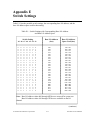
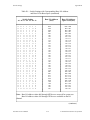
Switch Settings .....................................................................................................................E-1
Appendix F
Customer Communication ...............................................................................................F-1
Index .............................................................................................................................. Index-1
Figures
Figure 1-1.
PC-TIO-10 Interface Board ...............................................................................1-1
Figure
Figure
Figure
Figure
Figure
Figure
Figure
Figure
Figure
Figure
PC-TIO-10 Parts Locator Diagram ....................................................................2-2
Example Base I/O Address Switch Settings ......................................................2-3
Interrupt Jumper Setting for IRQ5 (Factory Setting) .........................................2-4
Interrupt Jumper Setting for Disabling Interrupts ..............................................2-5
Local Interrupt Jumper Setting (Factory Setting) ..............................................2-5
PC-TIO-10 I/O Connector Pin Assignments .....................................................2-7
Event-Counting Application with External Switch Gating................................2-10
Frequency Measurement Application ................................................................2-11
Timing Signal Relationships ..............................................................................2-12
Digital I/O Connections .....................................................................................2-14
2-1.
2-2.
2-3.
2-4.
2-5.
2-6.
2-7.
2-8.
2-9.
2-10.
Figure 3-1.
PC-TIO-10 Block Diagram ................................................................................3-1
Figure B-1.
PC-TIO-10 I/O Connector .................................................................................B-1
PC-TIO-10 User Manual
x
© National Instruments Corporation
Contents
Tables
Table 2-1.
Table 2-2.
PC-TIO-10 Factory-Set Switch and Jumper Settings ........................................2-1
Default Settings of National Instruments Products for the PC ..........................2-4
Table 4-1.
PC-TIO-10 Address Map ...................................................................................4-2
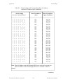
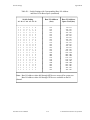
Table E-1.
Switch Settings with Corresponding Base I/O Address and Base I/O
Address Space ....................................................................................................E-1
© National Instruments Corporation
xi
PC-TIO-10 User Manual
Chapter 1
Introduction
This chapter describes the PC-TIO-10, lists the contents of your PC-TIO-10 kit, lists the optional
software and equipment for use with the PC-TIO-10, and explains how to unpack the PC-TIO-10
kit.
The PC-TIO-10 is a timing and digital I/O interface for the PC. Two AMD Am9513A STCs are
used for the timing interface. With these chips, which feature many different timing and
counting modes, the PC-TIO-10 can perform of a wide range of pulse measurement and wave
generation functions. A Motorola MC6821 PIA is used for the digital I/O interface; each of the
two 8-bit I/O ports is bit-configurable. In addition, the PC-TIO-10 has two edge-sensitive
interrupt inputs with programmable edge selection. Any external TTL signal, including any of
the counter outputs, can be connected to these interrupt inputs.
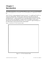
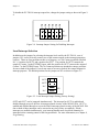
Figure 1-1 shows the PC-TIO-10 interface board.
Figure 1-1. PC-TIO-10 Interface Board
© National Instruments Corporation
1-1
PC-TIO-10 User Manual
Introduction
Chapter 1
The timing circuits on the board make the PC-TIO-10 useful for the following operations:
•
Wave and pulse generation
•
Frequency shift keying (FSK)
•
Pulse-width measurement
•
Time-of-day counting and alarm generation
•
Event counting
The digital I/O lines on the PC-TIO-10 interface the PC to the following:
•
BCD-compatible panel meters and test equipment
•
Opto-isolated, solid-state relays and I/O module mounting racks
The PC-TIO-10 turns the PC into a timing and digital I/O system controller for applications in
laboratory testing, production testing, and industrial process monitoring and control.
What Your Kit Should Contain
The contents of the PC-TIO-10 kit (part number 776452-01) are listed as follows.
Kit Component
Part Number
PC-TIO-10 board
PC-TIO-10 User Manual
NI-DAQ software for DOS/Windows/LabWindows, with manuals
NI-DAQ Software Reference Manual for DOS/Windows/LabWindows
NI-DAQ Function Reference Manual for DOS/Windows/LabWindows
181195-01
320292-01
776250-01
320498-01
320499-01
If your kit is missing any of the components, contact National Instruments.
Your PC-TIO-10 is shipped with the NI-DAQ software for DOS/Windows/LabWindows.
NI-DAQ has a library of functions that can be called from your application programming
environment. These functions include routines for analog input (A/D conversion), buffered data
acquisition (high-speed A/D conversion), analog output (D/A conversion), waveform generation,
digital I/O, counter/timer, SCXI, RTSI, and self-calibration. NI-DAQ maintains a consistent
software interface among its different versions so you can switch between platforms with
minimal modifications to your code. NI-DAQ comes with language interfaces for Professional
BASIC, Turbo Pascal, Turbo C, Turbo C++, Borland C++, and Microsoft C for DOS; and Visual
Basic, Turbo Pascal, Microsoft C with SDK, and Borland C++ for Windows. NI-DAQ software
is on high-density 5.25 in. and 3.5 in. diskettes.
PC-TIO-10 User Manual
1-2
© National Instruments Corporation
Chapter 1
Introduction
Optional Software
This manual contains complete instructions for directly programming the PC-TIO-10. Normally,
however, you should not need to read the low-level programming details in the user manual
because the NI-DAQ software package for controlling the PC-TIO-10 is included with the board.
Using NI-DAQ is quicker and easier than and as flexible as using the low-level programming
described in Chapter 4, Programming.
You can use the PC-TIO-10 with LabVIEW for Windows or LabWindows for DOS. LabVIEW
and LabWindows are innovative program development software packages for data acquisition
and control applications. LabVIEW uses graphical programming, whereas LabWindows
enhances Microsoft C and QuickBASIC. Both packages include extensive libraries for data
acquisition, instrument control, data analysis, and graphical data presentation.
Part numbers for these software packages are listed in the following table.
Software
Part Number
LabVIEW for Windows
LabWindows
Standard package
Advanced Analysis Library
Standard package with the Advanced Analysis Library
776670-01
776473-01
776474-01
776475-01
Optional Equipment
Equipment
Part Number
CB-50 I/O connector block – 0.5 m cable
CB-50 I/O connector block – 1.0 m cable
776164-01
776164-02
Standard ribbon cable – 0.5 m
Standard ribbon cable – 1.0 m
180524-05
180524-10
Shielded ribbon cable – 0.5 m
Shielded ribbon cable – 1.0 m
180554-05
180554-10
Refer to the Cabling section in Chapter 2 for additional information on cabling and connectors.
© National Instruments Corporation
1-3
PC-TIO-10 User Manual
Introduction
Chapter 1
Unpacking
Your PC-TIO-10 board is shipped in an antistatic package to prevent electrostatic damage to the
board. Several components on the board can be damaged by electrostatic discharge. To avoid
such damage in handling the board, take the following precautions:
•
Touch the antistatic package to a metal part of your computer chassis before removing the
board from the package.
•
Remove the board from the package and inspect the board for loose components or any other
sign of damage. Notify National Instruments if the board appears damaged in any way. Do
not install a damaged board into your computer.
PC-TIO-10 User Manual
1-4
© National Instruments Corporation
Chapter 2
Configuration and Installation
This chapter describes the PC-TIO-10 jumper configurations, installation of the PC-TIO-10
board in your computer, signal connections to the PC-TIO-10 board, and cabling instructions.
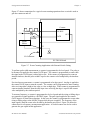
Board Configuration
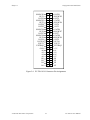
The PC-TIO-10 contains one DIP switch and two jumpers to configure the base I/O address and
interrupts, respectively. The DIP switch and jumpers are shown in the parts locator diagram in
Figure 2-1.
The PC-TIO-10 is configured at the factory to a base I/O address of hex 1A0, to interrupt
level 5, and to local interrupt setting No Connect and No Connect. These settings (shown in
Table 2-1) are suitable for most systems. However, if your system has other hardware at this
base I/O address or interrupt level, you need to change these settings on the PC-TIO-10 (as
described in the following pages) or on the other hardware. Record your settings in the PC-TIO10 Hardware and Software Configuration Form in Appendix F, Customer Communication.
Table 2-1. PC-TIO-10 Factory-Set Switch and Jumper Settings
Base I/O Address
U12
A9
A8
A7
A6
A5
A4
A3
1 2 3 4 5 6 7
Hex 1A0
(factory setting)
(The black side indicates the side of the
switch that is pushed down.)
Interrupt Level
Interrupt level 5 selected
(factory setting)
W1:
Row 5
Local Interrupt
No Connect and No Connect
(factory setting)
W2:
No Connect
No Connect
© National Instruments Corporation
2-1
PC-TIO-10 User Manual
Configuration and Installation
Chapter 2
Figure 2-1. PC-TIO-10 Parts Locator Diagram
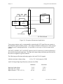
Base I/O Address Settings
The base I/O address for the PC-TIO-10 is determined by the switches at position U12 (see
Figure 2-1). The switches are set at the factory for the I/O address hex 1A0. With this default
setting, the PC-TIO-10 uses the I/O address space hex 1A0 through 1A7.
Note: Verify that this space is not already used by other equipment installed in your computer.
If any equipment in your computer uses this I/O address space, you must change the base
I/O address for the PC-TIO-10 or for the other device.
PC-TIO-10 User Manual
2-2
© National Instruments Corporation
Chapter 2
Configuration and Installation
Each switch in U12 corresponds to one of the address lines A9 through A3. Thus, the range for
possible base I/O address settings is hex 000 through 3F8. Base I/O address values hex 000
through 0FF are reserved for system use. Base I/O values hex 100 through 3FF are available on
the I/O channel. A2, A1, and A0 are used by the PC-TIO-10 to decode accesses to the onboard
registers. On the U12 DIP switches, press the side marked OFF to select a binary value of 1 for
the corresponding address bit. Press the other side of the switch to select a binary value of 0 for
the corresponding address bit. Figure 2-2 shows two possible switch settings. The black side
indicates the side of the switch that is pushed down.
U12
O
N
O
F
F
1
A9
2
A8
3
A7
4
A6
5
A5
6
A4
7
A3
A. Switches Set to Default Setting (Base I/O Address Hex 1A0)
U12
O
N
O
F
F
1
A9
2
A8
3
A7
4
A6
5
A5
6
A4
7
A3
B. Switches Set to Base I/O Address Hex 228
Figure 2-2. Example Base I/O Address Switch Settings
© National Instruments Corporation
2-3
PC-TIO-10 User Manual
Configuration and Installation
Chapter 2
Table 2-2. Default Settings of National Instruments Products for the PC
Board
DMA Channel
Interrupt Level
AT-A2150
AT-AO-6/10
AT-DIO-32F
AT-DSP2200
AT-GPIB
AT-MIO-16
AT-MIO-16D
AT-MIO-16F-5
AT-MIO-16X
AT-MIO-64F-5
GPIB-PCII
GPIB-PCIIA
GPIB-PCIII
Lab-PC
PC-DIO-24
PC-DIO-96
PC-LPM-16
PC-TIO-10
None*
Channel 5
Channels 5, 6
None*
Channel 5
Channels 6, 7
Channels 6, 7
Channels 6, 7
None*
None*
Channel 1
Channel 1
Channel 1
Channel 3
None
None
None
None
None*
Lines 11, 12
Lines 11, 12
None*
Line 11
Line 10
Lines 5, 10
Line 10
None*
None*
Line 7
Line 7
Line 7
Line 5
Line 5
Line 5
Line 5
Line 5
Base I/O Address
120 hex
1C0 hex
240 hex
120 hex
2C0 hex
220 hex
220 hex
220 hex
220 hex
220 hex
2B8 hex
02E1 hex
280 hex
260 hex
210 hex
180 hex
260 hex
1A0 hex
* These settings are software configurable and are disabled at startup time.
Interrupt Level Selection
There are two sets of jumpers for interrupt selection on the PC-TIO-10 board. W1 is used for
selecting the interrupt level, while W2 is used for local selection of two of the counter outputs as
interrupt sources. The locations of these jumpers are shown in Figure 2-1.
The PC-TIO-10 board can connect to any one of six interrupt lines of the PC I/O Channel:
IRQ3, IRQ4, IRQ5, IRQ6, IRQ7, or IRQ9. You select the interrupt line by setting a jumper on
W1. The default interrupt line is IRQ5. To change to another line, remove the jumper from
IRQ5 and place it on the pins for another request line. Figure 2-3 shows the default factory
setting for IRQ5.
IRQ9
IRQ7
IRQ6
IRQ5
IRQ4
IRQ3
W1
IRQ3
IRQ9
Figure 2-3. Interrupt Jumper Setting for IRQ5 (Factory Setting)
PC-TIO-10 User Manual
2-4
© National Instruments Corporation
Chapter 2
Configuration and Installation
To disable the PC-TIO-10 interrupt request line, change the jumper setting as shown in Figure 24.
IRQ9
IRQ7
IRQ6
IRQ5
IRQ4
IRQ3
W1
IRQ3
IRQ9
Figure 2-4. Interrupt Jumper Setting for Disabling Interrupts
Local Interrupt Selection
In addition to the jumpers for selecting the interrupt level used by the PC-TIO-10, a set of
jumpers, W2, is used to locally connect two of the counter outputs to the interrupt generation
circuitry. There are four positions on this set of jumpers: two No Connect positions (labelled
N.C.), a position for OUT2, and a position for OUT7. The position for OUT2 connects the
output of Counter 2 to the EXTIRQ1 input, while the position for OUT7 connects the output of
Counter 7 to the EXTIRQ2 input. The No Connect positions are intended as storage positions
for one or both of the jumpers if you do not want to use one or both of the counter outputs for
interrupt purposes. The default positions for the jumpers on W2 are shown in Figure 2-5.
OUT2
OUT7
N.C.
W2
N.C.
Figure 2-5. Local Interrupt Jumper Setting (Factory Setting)
OUT2 and OUT7 can be jumpered simultaneously. The interrupt for OUT2 is enabled and
disabled through access to the Port A interrupt-control circuitry of the MC6821 PIA. OUT7 is
enabled and disabled through access to the Port B interrupt-control circuitry of the MC6821 PIA.
One or both of these interrupts can be asserted at any time (if they are enabled). If both
interrupts are enabled simultaneously, your interrupt handler must check both channels for
interrupts before returning control to the foreground task. For more information, see Chapter 4,
Programming.
© National Instruments Corporation
2-5
PC-TIO-10 User Manual
Configuration and Installation
Chapter 2
Installation
The PC-TIO-10 can be installed in any unused 8-bit, 16-bit, or 32-bit expansion slot in your
computer. After you make any necessary changes and verify the switch and jumper settings,
record them in the PC-TIO-10 Hardware and Software Configuration Form in Appendix F,
Customer Communication. You are now ready to install the PC-TIO-10.
The following are general installation instructions, but consult the user manual or technical
reference manual of your personal computer for specific instructions and warnings. If you want
to install this board in an EISA-class computer, you can obtain a configuration file for the board
by contacting National Instruments.
1.
Turn off your computer.
2.
Remove the top cover or access port to the I/O channel.
3.
Remove the expansion slot cover on the back panel of the computer.
4.
Insert the PC-TIO-10 in an unused 8-bit, 16-bit, or 32-bit slot. It may be a tight fit, but do
not force the board into place.
5.
Screw the mounting bracket of the PC-TIO-10 to the back panel rail of the computer.
6.
Check the installation.
7.
Replace the cover to the computer.
Note: If you have an ISA-class computer and you are using a configurable software package,
such as NI-DAQ, you may need to reconfigure your software to reflect any changes in
jumper or switch settings. If you have an EISA-class computer, you need to update the
computer's resource allocation (or configuration) table by reconfiguring your computer.
See your computer's user manual for information about updating the configuration table.
The PC-TIO-10 board is now installed and ready for operation.
Signal Connections
This section includes specifications and connection instructions for the signals given on the
PC-TIO-10 I/O connector.
Warning: Connections that exceed any of the maximum ratings of input or output signals on
the PC-TIO-10 may result in damage to the PC-TIO-10 board and to the PC.
Maximum input ratings for each signal are given in this chapter under the discussion
of that signal. National Instruments is not liable for any damages resulting from any
such signal connections.
I/O Connector Pin Description
Figure 2-6 show the pin assignments for the PC-TIO-10 I/O connector.
PC-TIO-10 User Manual
2-6
© National Instruments Corporation
Chapter 2
Configuration and Installation
SOURCE1
OUT1
GATE2
SOURCE3
OUT3
GATE4
GATE5
SOURCE6
OUT6
GATE7
SOURCE8
OUT8
GATE9
GATE10
FOUT1
EXTIRQ1
GND
A0
A2
A4
A6
B0
B2
B4
B6
1
3
5
7
9
11
13
15
17
19
21
23
25
27
29
31
33
35
37
39
41
43
45
47
49
2
4
6
8
10
12
14
16
18
20
22
24
26
28
30
32
34
36
38
40
42
44
46
48
50
GATE1
SOURCE2
OUT2
GATE3
SOURCE4
OUT4
OUT5
GATE6
SOURCE7
OUT7
GATE8
SOURCE9
OUT9
OUT10
FOUT2
EXTIRQ2
+5 V
A1
A3
A5
A7
B1
B3
B5
B7
Figure 2-6. PC-TIO-10 I/O Connector Pin Assignments
© National Instruments Corporation
2-7
PC-TIO-10 User Manual
Configuration and Installation
Chapter 2
Signal Connection Descriptions
Pins
Signal Names
Description
1, 4, 7,
10, 15, 18,
21, 24
SOURCE<1..4>
SOURCE<6..9>
These are the source inputs for Counters 1
through 4 and Counters 6 through 9.
The source inputs for Counters 5 and 10 do
not appear on the I/O connector because
are internally connected to a 5-MHz clock.
2, 5, 8, 11,
13, 16, 19,
22, 25, 27
GATE<1..10>
These are the gate inputs for Counters 1
through 10.
3, 6, 9, 12,
14, 17, 20,
23, 26, 28
OUT<1..10>
These are the outputs for Counters 1
through 10.
29-30
FOUT<1..2>
These are the frequency outputs of the two
Am9513A devices.
31-32
EXTIRQ<1..2>
These are the interrupt inputs
for the PC-TIO-10.
33
GND
This pin is connected to the computer's
ground signal.
34
+5 V
This pin is connected to the computer's
+5 VDC power supply.
35-42
A
A<0..7>
These are the eight digital I/O lines on Port
of the MC6821. The MSB is A7.
43-50
B
B<0..7>
These are the eight digital I/O lines on Port
of the MC6821. The MSB is B7.
they
PC-TIO-10 User Manual
2-8
© National Instruments Corporation
Chapter 2
Configuration and Installation
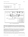
Timing Signal Connections
Pins 1 through 30 of the I/O connector are connections for timing I/O signals on the two onboard
Am9513A Counter/Timers. The timing signals include the GATE, SOURCE, and OUT signals
for the Am9513A Counters 1 through 10, and the FOUT1 and FOUT2 signals generated by the
Am9513A STCs. Counters 1 through 10 of the Am9513A Counter/Timers can be used for
general-purpose applications, such as pulse and square wave generation, event counting, and
pulse-width, time-lapse, and frequency measurements. For these applications, SOURCE and
GATE signals can be directly applied to the counters from the I/O connector, and the counters
are programmed for various operations.
The Am9513A Counter/Timer is described briefly in Chapter 3, Theory of Operation. For
detailed programming information, consult Appendix C, AMD Am9513A Data Sheet. For
detailed applications information, consult the Am9513A/Am9513A System Timing Controller
technical manual published by Advanced Micro Devices, Inc.
Pulses and square waves can be produced by programming a counter to generate a pulse signal at
its OUT pin or to toggle the OUT signal each time the counter reaches the terminal count.
For event counting, one of the counters is programmed to count rising or falling edges applied to
any of the Am9513A SOURCE inputs. The counter value can then be read to determine the
number of edges that have occurred. Counter operation can be gated on and off during event
counting.
© National Instruments Corporation
2-9
PC-TIO-10 User Manual
Configuration and Installation
Chapter 2
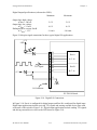
Figure 2-7 shows connections for a typical event-counting operation where a switch is used to
gate the counter on and off.
Counter
SOURCE
+5 V
OUT
GATE
Switch
Signal
Source
33
GND
I/O Connector
PC-TIO-10 Board
Figure 2-7. Event-Counting Application with External Switch Gating
To perform pulse-width measurement, a counter is programmed to be level-gated. The pulse to
be measured is applied to the counter GATE input. The counter is programmed to count while
the signal at the GATE input is either high or low. If the counter is programmed to count an
internal timebase, then the pulse width is equal to the counter value multiplied by the timebase
period.
For time-lapse measurement, a counter is programmed to be edge-gated. An edge is applied to
the counter GATE input to start the counter. The counter can be programmed to start counting
after receiving either a high-to-low edge or a low-to-high edge. If the counter is programmed to
count an internal timebase, then the time lapse since receiving the edge is equal to the counter
value multiplied by the timebase period.
To measure frequency, a counter is programmed to be level-gated and the rising or falling edges
are counted in a signal applied to a SOURCE input. The gate signal applied to the counter
GATE input is of some known duration. In this case, the counter is programmed to count either
rising or falling edges at the SOURCE input while the gate is applied. The frequency of the
input signal is then the count value divided by the known gate period. Figure 2-8 shows the
connections for a frequency measurement application. A second counter can also be used to
generate the gate signal in this application.
PC-TIO-10 User Manual
2-10
© National Instruments Corporation
Chapter 2
Configuration and Installation
Counter
SOURCE
OUT
GATE
Signal
Source
Gate
Source
33
GND
I/O Connector
PC-TIO-10 Board
Figure 2-8. Frequency Measurement Application
Two or more counters can be concatenated by connecting the OUT signal from one counter to
the SOURCE signal of another counter. The counters can then be treated as one 32-bit or larger
counter for most counting applications. It is possible to create up to a 160-bit counter in this
manner.
The GATE, SOURCE, OUT, and FOUT signals on the I/O connector are connected directly to
the Am9513A input and output pins. The input and output ratings and timing specifications for
the Am9513A signals are given as follows.
The following specifications and ratings apply to the Am9513A I/O signals.
Absolute maximum voltage rating
-0.5 to +7.0 V with respect to GND
Am9513A Digital Input Specifications (referenced to GND):
Minimum
Input logic high voltage
Input logic low voltage
Input current (0 < Vin < 5.25 V)
© National Instruments Corporation
2.0 V
0.0 V
-10 µA
2-11
Maximum
5.25 V
0.8 V
10 µA
PC-TIO-10 User Manual
Configuration and Installation
Chapter 2
Am9513A Digital Output Specifications (referenced to GND):
Minimum
Maximum
2.4 V
5.0 V
0.0 V
0.4 V
Output logic high voltage, all outputs
at Iout = -200 µA
Output logic low voltage, all outputs
at Iout = 3.2 mA
Figure 2-9 shows the timing requirements for the GATE and SOURCE input signals and the
timing specifications for the OUT signals of the Am9513A STCs.
t sc
V
SOURCE I H
VI L
V
GATE I H
VI L
V
OUT I H
VI L
t gsu
t sp
t sp
t gh
t gw
t out
t sc
t sp
t gsu
t gh
t gw
t out
145 nsec
70 nsec
100 nsec
10 nsec
145 nsec
300 nsec
Minimum
Minimum
Minimum
Minimum
Minimum
Maximum
Figure 2-9. Timing Signal Relationships
The GATE and OUT signal transitions in Figure 2-9 are referenced to the rising edge of the
SOURCE signal. This timing diagram assumes that the counters are programmed to count rising
edges. The same timing diagram, with the source signal inverted and referenced to the falling
edge of the source signal, applies to the case in which the counter is programmed to count falling
edges.
The signal applied at a SOURCE input can be used as a clock source by any of the Am9513A
counter/timers and by the Am9513A frequency division output FOUT. The signal applied to a
SOURCE input must not exceed a frequency of 7 MHz for proper operation of the Am9513A.
The Am9513A counters can be individually programmed to count rising or falling edges of
signals applied at any of the Am9513A SOURCE or GATE input pins.
In addition to the signals applied to the SOURCE and GATE inputs, the Am9513A generates
five internal timebase clocks from the clock signal supplied by the PC-TIO-10. The five internal
PC-TIO-10 User Manual
2-12
© National Instruments Corporation
Chapter 2
Configuration and Installation
timebase clocks can be used as counting sources, and these clocks have a maximum skew of
75 nsec between them. The SOURCE signal shown in Figure 2-9 represents any of the signals
applied at the SOURCE inputs, GATE inputs, or internal timebase clocks. See the Am9513A
data sheet in Appendix C for further details.
Specifications for signals at the GATE input are referenced to the signal at the SOURCE input or
one of the Am9513A internally generated signals. Figure 2-9 shows the GATE signal referenced
to the rising edge of a source signal. The gate must be valid (either high or low) at least 100 nsec
before the rising or falling edge of a source signal for the gate to take effect at that source edge
(as shown by tgsu and tgh in Figure 2-9). Similarly, the gate signal must be held for at least 10
nsec after the rising or falling edge of a source signal for the gate to take effect at that source
edge. The gate high or low period must be at least 145 nsec in duration. If an internal timebase
clock is used, the gate signal cannot be synchronized with the clock. In this case, gates applied
close to a source edge take effect either on that source edge or on the next one. This arrangement
creates an uncertainty of one source clock period with respect to unsynchronized gating sources.
Signals generated at the OUT pin are referenced to the signal at the SOURCE input or to one of
the Am9513A internally generated clock signals. Figure 2-9 shows the OUT signal referenced to
the rising edge of a source signal. Any OUT signal state changes occur within 300 nsec after the
source signal's rising or falling edge.
Digital I/O Signal Connections
Pins 31, 32, and 35 through 50 of the I/O connector are digital I/O signal pins.
Pins 35 through 42 are connected to the digital lines A<0..7> for digital I/O Port A. Pins 43
through 50 are connected to the digital lines B<0..7> for digital I/O Port B. Pins 31 and 32 are
connected to the external interrupt lines, EXTIRQ1 and EXTIRQ2. Ports A and B can be
programmed on a bitwise basis to be inputs or outputs.
The following specifications and ratings apply to the digital I/O lines.
Absolute maximum voltage rating
-0.3 to +7.0 V with respect to GND
Digital Input Specifications (referenced to GND):
Input logic high voltage
Input logic low voltage
Input current, Port A
(0 < Vin < 0.8 V)
Input current, Port A
(2.0 < Vin < 5.25 V)
Input current, Port B
(0.4 < Vin < 2.4 V)
Input current, EXTIRQ1 and EXTIRQ2
(0 < Vin < 5.25 V)
© National Instruments Corporation
Minimum
Maximum
2.0 V
0.0 V
5.25 V
0.8 V
–
-2.4 mA
–
-400 µA
–
10 µA
–
2-13
2.5 µA
PC-TIO-10 User Manual
Configuration and Installation
Chapter 2
Digital Output Specifications (referenced to GND):
Output logic high voltage
at Iout = -200 µA
Output logic low voltage
at Iout = 3.2 mA
Darlington drive current, Port B
at VEXT = 1.5 V
Minimum
Maximum
2.4 V
5.0 V
0.0 V
0.4 V
-1.0 mA
-10.0 mA
Figure 2-10 depicts signal connections for three typical digital I/O applications.
+5 V
LED
38
37
36
35
50
49
48
47
TTL Signal
+5 V
Port A
A<3..0>
Port B
B<7..4>
Switch
33
GND
I/O Connector
PC-TIO-10 Board
Figure 2-10. Digital I/O Connections
In Figure 2-10, Port A is configured for digital output, and Port B is configured for digital input.
Digital input applications include receiving TTL signals and sensing external device states such
as the state of the switch in Figure 2-10. Digital output applications include sending TTL signals
and driving external devices such as the LED shown in Figure 2-10.
PC-TIO-10 User Manual
2-14
© National Instruments Corporation
Chapter 2
Configuration and Installation
Power Connections
Pin 34 of the I/O connector is connected to the +5 V supply from the PC power supply. This pin
is referenced to GND and can be used to power external digital circuitry. For more information
on this output pin, see Output Signal Specifications in Appendix A, Specifications.
Power Rating
1.0 A at +5 V ± 10%
Warning: Under no circumstances should this +5-V power pin be connected directly to ground
or to any other voltage source on the PC-TIO-10 or any other device. Doing so may
damage the PC-TIO-10 and the PC. National Instruments is not liable for damage
resulting from such a connection.
Cabling
The PC-TIO-10 digital I/O connector is a standard, 50-pin, header connector, which can be
interfaced using 50-pin ribbon cable with appropriate connectors. The CB-50 cable termination
accessory is available from National Instruments for use with the PC-TIO-10 board. This kit
includes a 50-conductor, flat ribbon cable and a connector block. Signal input and output wires
can be attached to screw terminals on the connector block and are therefore connected to the
PC-TIO-10 I/O connector.
The CB-50 is useful for initial prototyping of an application or in situations where PC-TIO-10
interconnections are frequently changed. Once a final field wiring scheme has been developed,
however, you may want to develop your own cable. This section contains information for the
design of custom cables.
The PC-TIO-10 I/O connector is a 50-pin, male, ribbon-cable header connector. The
manufacturers and the appropriate part numbers for this connector are as follows:
•
Electronic Products Division/3M (part number 3596-5002)
•
T&B/Ansley Corporation (part number 609-5007)
The mating connector for the PC-TIO-10 is a 50-position, polarized, ribbon-socket connector
with strain relief. National Instruments uses a polarized (keyed) connector to prevent inadvertent
upside-down connection to the PC-TIO-10. Recommended manufacturers and the appropriate
part numbers for this mating connector are as follows:
•
Electronic Products Division/3M (part number 3425-7650)
•
T&B/Ansley Corporation (part number 609-5041CE)
Recommended manufacturer part numbers for the standard ribbon cable (50-conductor, 28
AWG, stranded) that can be used with these connectors are as follows:
•
Electronic Products Division/3M (part number 3365/50)
•
T&B/Ansley Corporation (part number 171-50)
© National Instruments Corporation
2-15
PC-TIO-10 User Manual
Chapter 3
Theory of Operation
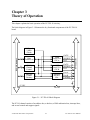
This chapter explains the basic operation of the PC-TIO-10 circuitry.
The block diagram in Figure 3-1 illustrates the key functional components of the PC-TIO-10
board.
GATE
5
SOURCE 4
OUT
6
8
Data
Transceiver
AMD
Am9513A
STC A
21
PC I/O
Channel
Control
AMD
Am9513A
STC B
GATE
5
SOURCE 4
OUT
6
6
Interrupt
Control
Circuitry
Motorola
MC6821
PIA
Port A
8
Port B
8
EXTIRQ 2
I/O Connector
PC I/O Channel
1-MHz and
5-MHz
Clocks
+5 VDC
1A Fuse
Figure 3-1. PC-TIO-10 Block Diagram
The PC I/O channel consists of an address bus, a data bus, a DMA arbitration bus, interrupt lines,
and several control and support signals.
© National Instruments Corporation
3-1
PC-TIO-10 User Manual
Theory of Operation
Chapter 3
Data Transceivers
The data transceivers control the sending and receiving of data to and from the PC I/O Channel.
PC I/O Channel Control Circuitry
The base address used by the board is determined by an onboard switch setting. The address on
the PC I/O channel bus is monitored by the address decoder, which is part of the I/O channel
control circuitry. If the address on the bus matches the selected I/O base address of the board,
the board is enabled and the corresponding register on the PC-TIO-10 is accessed.
In addition, the I/O channel control circuitry monitors and transmits the PC I/O channel control
and support signals. The control signals identify transfers as read or write, memory or I/O, and
8-bit, 16-bit, or 32-bit transfers. The PC-TIO-10 uses only 8-bit transfers.
Am9513A System Timing Controller
The Am9513A STCs are the heart of the PC-TIO-10. These chips have five individuallycontrolled 16-bit counters, each of which can be configured to operate in a number of different
modes. Therefore, the PC-TIO-10 can be used for applications such as rate generation, FSK, and
pulse parameter measurement. Each of the counters has its own source (SOURCE), gate
(GATE), and output (OUT) connections. Each STC has an independently-controlled, frequencyscaler output. The STCs are clocked by an onboard 1-MHz crystal oscillator to give 1-µsec
timing resolution. In addition, SOURCE5 and SOURCE10 are clocked at 5 MHz to give 200nsec resolution on all timing channels. Refer to Chapter 4, Programming, or to Appendix C,
AMD Am9513A Data Sheet, for more detailed information.
MC6821 Peripheral Interface Adapter
The MC6821 PIA features sixteen bits of bit-configurable digital I/O. In addition, this device
has two edge-programmable interrupt inputs, with which the PC-TIO-10 can receive external
interrupts. Refer to Chapter 4, Programming, or to Appendix D, Motorola MC6821 Data Sheet,
for more detailed information.
Interrupt Control Circuitry
The interrupt level used by the PC-TIO-10 is selected by the onboard jumper W1. Interrupts can
be generated from two different sources, EXTIRQ1 and EXTIRQ2, each of which has
programmable-edge polarity and individual enable, clear, and disable commands. A second set
of jumpers, W2, locally connects two of the counter outputs to the interrupt circuitry. With these
connections, external wrap-backs are unnecessary if you want to use a counter to generate timed
interrupts. Refer to Chapter 4, Programming, or to Appendix D, Motorola MC6821 Data Sheet,
for more detailed information on controlling interrupts. Refer to Chapter 2, Configuration and
Installation, for more information on configuring the jumper settings.
PC-TIO-10 User Manual
3-2
© National Instruments Corporation
Chapter 3
Theory of Operation
Timing and Digital I/O Connector
All timing and digital I/O is transmitted through a standard, 50-pin, male connector. Pin 34 is
connected to +5 V through a protection fuse (F1). This +5 V supply is often required to operate
I/O module mounting racks. Pin 33 is connected to ground. See Chapter 2, Configuration and
Installation, for additional information.
© National Instruments Corporation
3-3
PC-TIO-10 User Manual
Chapter 4
Programming
This chapter describes in detail the address and function of each of the PC-TIO-10 control and
status registers. This chapter also includes important information about programming the
PC-TIO-10.
The PC-TIO-10 is a timing and digital I/O board designed around two Am9513A integrated
circuits and one MC6821 integrated circuit. The Am9513A is a general-purpose counter/timer
with five 16-bit, individually-controlled counters and a 4-bit frequency-scaler output. The
MC6821 is a
16-bit, bit-configurable, digital I/O device with two interrupt inputs that are edge-programmable.
This chapter includes programming information for the PC-TIO-10, along with program
examples written in C and assembly language.
Note: If you plan to use a programming software package such as LabWindows or NI-DAQ
with your PC-TIO-10 board, you need not read this chapter.
Introduction
Each of the two Am9513A STC devices is controlled by three different registers–a data register,
a command register, and a status register. These registers are defined later in this chapter.
Because there are two Am9513A STC devices on the board, they are referenced as STC A and
STC B when differentiation is required.
The MC6821 PIA has four different registers that control its operation. The 16 I/O lines are
grouped into two 8-bit ports, Port A and Port B, each of which has a control register and a data
register associated with it. These registers are defined later in this chapter.
For clarification, both registers and ports are referenced in the sections that follow. A register
refers to a given 8-bit or 16-bit register on the actual Am9513A STC or MC6821 PIA, whereas a
port refers to the I/O channel register through which the device must be accessed. Therefore, the
size shown for a register indicates both the register size and the I/O channel port size. The digital
I/O ports associated with the MC6821 PIA are always referenced as Port A and Port B.
© National Instruments Corporation
4-1
PC-TIO-10 User Manual
Programming
Chapter 4
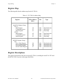
Register Map
The following table lists the address map for the PC-TIO-10.
Table 4-1. PC-TIO-10 Address Map
Register
Offset Address
(Hex)
Am9513A Register Group
STC A
Data Register
Command Register
Status Register
STC B
Data Register
Command Register
Status Register
MC6821 Register Group
PIA
Port A Data Register
Port A Control Register
Port B Data Register
Port B Control Register
Size
Type
00
01
01
8-bit
8-bit
8-bit
Read-and-write
Write-only
Read-only
02
03
03
8-bit
8-bit
8-bit
Read-and-write
Write-only
Read-only
04
05
06
07
8-bit
8-bit
8-bit
8-bit
Read-and-write
Read-and-write
Read-and-write
Read-and-write
Register Descriptions
The register descriptions for the devices on the PC-TIO-10, including the Am9513A STCs and
the MC6821 PIA, are given on the pages that follow.
PC-TIO-10 User Manual
4-2
© National Instruments Corporation
Chapter 4
Programming
Register Descriptions for the Am9513A STCs
Each of the two Am9513A STC devices has three registers–a data register, a command register,
and a status register. The bit maps and signal definitions for each of these registers are as
follows. Counters 1, 2, 3, 4, and 5 map to Counters 1, 2, 3, 4, and 5 of STC A, respectively;
Counters 6, 7, 8, 9, and 10 map to Counters 1, 2, 3, 4, and 5 of STC B, respectively.
© National Instruments Corporation
4-3
PC-TIO-10 User Manual
Programming
Chapter 4
Am9513A Data Registers
The Am9513A Data Registers are used to read from or write to any of the 18 internal registers of
the Am9513A. The Am9513A Command Registers must be written to in order to select the
register to be accessed by the Am9513A Data Registers. The internal registers accessed by the
Am9513A Data Registers are as follows:
•
Counter Mode Registers for Counters 1, 2, 3, 4, and 5
•
Counter Load Registers for Counters 1, 2, 3, 4, and 5
•
Counter Hold Registers for Counters 1, 2, 3, 4, and 5
•
Compare Registers for Counters 1 and 2
•
Master Mode Register
All these registers are 16-bit registers that must be accessed through an 8-bit port, least
significant byte first. Bit descriptions for each of these registers are included in Appendix C,
AMD Am9513A Data Sheet.
Address:
Base address + 00 (hex) for Am9513A STC A
Base address + 02 (hex) for Am9513A STC B
Type:
Read-and-write
Word Size:
16-bit register, 8-bit port
Bit Map:
7
6
5
4
3
2
1
0
D15
D14
D13
D12
D11
D10
D9
D8
7
6
5
4
3
2
1
0
D7
D6
D5
D4
D3
D2
D1
D0
Bit
Name
Description
7-0
D<15..8>
These eight bits are the most significant byte to be loaded into or
read from the Am9513A Internal Register currently selected.
These eight bits should be accessed after the eight bits of the least
significant byte are accessed.
7-0
D<7..0>
These eight bits are the least significant byte to be loaded into or
read from the Am9513A Internal Register currently selected.
These eight bits should be accessed before the eight bits of the
most significant byte are accessed.
PC-TIO-10 User Manual
4-4
© National Instruments Corporation
Chapter 4
Programming
Am9513A Command Registers
The Am9513A Command Registers control the overall operation of the Am9513A
Counter/Timer and selection of the internal registers that are accessed through the Am9513A
Data Registers.
Address:
Base address + 01 (hex) for Am9513A STC A
Base address + 03 (hex) for Am9513A STC B
Type:
Write-only
Word Size:
8-bit register, 8-bit port
Bit Map:
7
6
5
4
3
2
1
0
C7
C6
C5
C4
C3
C2
C1
C0
Bit
Name
Description
7-0
C<7..0>
These eight bits are loaded into the Am9513A Command Register.
See Appendix C, Am9513A Data Sheet, for detailed bit
descriptions of the Am9513A Command Registers.
© National Instruments Corporation
4-5
PC-TIO-10 User Manual
Programming
Chapter 4
Am9513A Status Registers
The Am9513A Status Registers give information about the output pin status of each counter in
the Am9513A. In addition, these registers indicate the current setting of the byte pointer, which
indicates whether the next byte to be accessed is the most significant byte or the least significant
byte.
Address:
Base address + 01 (hex) for Am9513A STC A
Base address + 03 (hex) for Am9513A STC B
Type:
Read-only
Word Size:
8-bit register, 8-bit port
Bit Map:
7
6
5
4
3
2
1
0
X
X
OUT5
OUT4
OUT3
OUT2
OUT1
BYTE POINTER
Bit
Name
Description
7-6
X
Unused bits. They may be returned as 0 or 1.
5-1
OUT<5..1>
Each of these five bits returns the logic state of the associated
counter output pin. For example, if the bit OUT4 is set, then the
output pin of Counter 4 (or Counter 9) is at a logic-high state.
0
BYTE POINTER
This bit represents the state of the Am9513A Byte Pointer FlipFlop. If this bit is set, the next byte to be written to or read from
the Data Port is the least significant byte; if this bit is clear, the
next byte to be written to or read from the Data Port is the most
significant byte.
PC-TIO-10 User Manual
4-6
© National Instruments Corporation
Chapter 4
Programming
Register Descriptions for the MC6821
The MC6821 PIA has four registers–Port A and Port B both have a Data Register and a Control
Register. The bit maps and signal definitions for each of these registers are as follows. For more
information on the various registers, refer to Appendix D, Motorola MC6821 Data Sheet.
© National Instruments Corporation
4-7
PC-TIO-10 User Manual
Programming
Chapter 4
MC6821 Data Registers
The MC6821 Data Registers are used to read from or write to the Output Registers (the
I/O registers for Ports A and B) and the Data Direction Registers.
Address:
Base address + 04 (hex) for Port A
Base address + 06 (hex) for Port B
Type:
Read-and-write
Word Size:
8-bit register, 8-bit port
Bit Map:
7
6
5
4
3
2
1
0
D7
D6
D5
D4
D3
D2
D1
D0
Bit
Name
Description
7-0
D<7..0>
If the Output Register is being accessed (see the description of the
Control Registers on the page that follows), writing a value to the
Data Register updates all output bits and has no effect on input
bits. Reading the Data Register returns the current signal value of
all bits, including those configured for output. If the Data
Direction Register is being accessed, writing a zero to a bit makes
the corresponding I/O line an input, while writing a one to a bit
makes the corresponding I/O line an output. Reading the Data
Direction Register returns the current configuration.
PC-TIO-10 User Manual
4-8
© National Instruments Corporation
Chapter 4
Programming
MC6821 Control Registers
The MC6821 Control Registers control the overall operation of the MC6821 and the selection of
the two internal registers that are accessed through each of the MC6821 Data Registers. Some of
the bits in the Control Registers are not used because of the design of the PC-TIO-10. These bits
should be set as follows.
Address:
Base address + 05 (hex) for Port A
Base address + 07 (hex) for Port B
Type:
Read-and-write
Word Size:
8-bit register, 8-bit port
Bit Map:
7
6
5
4
3
2
1
0
IRQ
0
0
0
0
DRS
EDGE
INTEN
Bit
Name
Description
7
IRQ
This is a read-only bit that reflects the current status of the
interrupt input for the selected Control Register. If this bit is one
in the
Port A Control Register, an interrupt request is pending on the
external interrupt line EXTIRQ1. If this bit is one in the Port B
Control Register, an interrupt request is pending on the external
interrupt line EXTIRQ2. Always write a zero to this bit.
6-3
Reserved
These bits are not used on the PC-TIO-10. Always write a zero to
each of these bits.
2
DRS
This is the Data Register Select bit. Writing a one to this bit
selects the Output Register, while writing a zero to this bit selects
the Data Direction Register. Reading this bit shows the bit's
current state. Refer to the description of the Data Register for
more information.
1
EDGE
This is the control bit for selecting the edge that will cause an
interrupt. Writing a one to this bit selects rising-edge interrupts,
while writing a zero to this bit selects falling-edge interrupts. The
Port A Control Register controls external interrupt line EXTIRQ1,
while the Port B Control Register controls external interrupt line
EXTIRQ2. Reading this bit shows the bit's current state.
0
INTEN
This bit enables and disables the interrupt generation capability of
EXTIRQ1 or EXTIRQ2. Writing a one to this bit enables
interrupts, while writing a zero to this bit disables interrupts. The
Port A Control Register controls EXTIRQ1, while the Port B
Control Register controls EXTIRQ2. Reading this bit shows the
bit's current state.
© National Instruments Corporation
4-9
PC-TIO-10 User Manual
Programming
Chapter 4
Programming Considerations for the Am9513A STCs
Before using the Am9513A STC devices, you must initialize them. To do this, perform the
following steps on each of the Am9513A STC devices. All writes are 8-bit write operations. All
values are given in hexadecimal.
1. Issue a master reset by writing FF to the Am9513A Command Register.
2. Initialize all five counters. For ctr = 1 to 5, follow these steps:
•
Write ctr to the Am9513A Command Register (select the Counter Mode Register).
•
Write 00 to the Am9513A Data Register (store the least significant byte of the counter
mode value).
•
Write 00 to the Am9513A Data Register (store the most significant byte of the counter
mode value).
•
Write ctr + 8 to the Am9513A Command Register (select the Counter Load Register).
•
Write 03 to the Am9513A Data Register (store the least significant byte of the counter
load value).
•
Write 00 to the Am9513A Data Register (store the most significant byte of the counter
load value).
3. Load all counters with their Counter Load Register values by writing 5F to the Am9513A
Command Register.
Note: When you initialize Am9513A STC B, which contains Counters 6 through 10, ctr must
range from 1 to 5, not from 6 to 10. Also, each Am9513A STC must always be
configured to use the 8-bit bus mode in order to function properly.
Programming Example for the Am9513A STCs
The code below lists a sample function that can be used to reset the Am9513A STCs on the
PC-TIO-10. In addition, the code lists a sample function that can be used to generate a variable
duty-cycle square-wave.
/*
miscellaneous definitions
#define
#define
#define
#define
#define
#define
#define
/*
cmd_port
data_port
no_err
range_err
stc_a
stc_b
tio_ba
*/
0x0001
0x0000
0
-1
0x0000
0x0002
0x01a0
function prototypes */
PC-TIO-10 User Manual
4-10
© National Instruments Corporation
Chapter 4
void
void
int
Programming
/*
main(void);
reset9513(unsigned int, unsigned int);
square_wave(unsigned int, unsigned int, unsigned int, unsigned long,
unsigned long);
support functions
*/
void
reset9513(base_address, chip_offset)
unsigned int
base_address,
chip_offset;
{
unsigned int
cmd,
data;
int
ctr;
/*
set up the register addresses
*/
cmd = base_address | chip_offset | cmd_port;
data = base_address | chip_offset | data_port;
/*
reset the 9513
*/
outp(cmd, 0xff);
for (ctr = 1; ctr <=5; ctr++)
{
outp(cmd, ctr);
outp(data, 0x00);
outp(data, 0x00);
outp(cmd, (ctr + 8));
outp(data, 0x03);
outp(data, 0x00);
}
outp(cmd, 0x5f);
/*
reset the chip
*/
/*
/*
/*
/*
/*
/*
select Counter Mode Register
store mode low-byte */
store mode high-byte
*/
select Counter Load Register
store load low-byte */
store load high-byte
*/
/*
load all counters
*/
*/
*/
}
int square_wave(base_address, counter, timebase, high_time, low_time)
unsigned int
base_address,
counter,
timebase;
unsigned long
high_time,
low_time;
{
unsigned int
cmd,
data,
mode;
/*
check ranges
*/
if ((counter < 1) || (counter > 10) ||
(timebase > 15) ||
(high_time < 1L) || (high_time > 65536L) ||
(low_time < 1L) || (low_time > 65536L))
return range_err;
/*
set up the register addresses
© National Instruments Corporation
4-11
*/
PC-TIO-10 User Manual
Programming
Chapter 4
cmd = base_address | ((counter > 5) ? stc_b : stc_a) | cmd_port;
data = base_address | ((counter > 5) ? stc_b : stc_a) | data_port;
/*
adjust some parameters and program the counter
*/
if (counter > 5)
counter -= 5;
mode = 0x0062 | (timebase << 8);
if (high_time == 65536L)
high_time = 0L;
if (low_time == 65536L)
low_time = 0L;
/*
5 ctrs per chip */
/*
/*
/*
/*
/*
counter mode
count of 65,536
goes to 0
count of 65,536
goes to 0
*/
*/
*/
*/
*/
outp(cmd, (0xc0 | (0x01 << (counter - 1))));
outp(cmd, counter);
outp(data, mode);
/*
/*
/*
*/
*/
outp(data, (mode >> 8));
/*
outp(cmd, (counter + 0x08));
outp(data, ((unsigned int) high_time));
/*
/*
outp(data, ((unsigned int) (high_time >> 8)));
/*
outp(cmd, (counter + 0x10));
outp(data, ((unsigned int) low_time));
/*
/*
outp(data, ((unsigned int) (low_time >> 8)));
/*
outp(cmd, (0x40 | (0x01 << (counter - 1))));
outp(cmd, (0xe8 | counter));
outp(cmd, (0x20 | (0x01 << (counter - 1))));
/*
/*
/*
disarm the ctr
select Mode Reg
send mode
low-byte
send mode
high-byte
select Load Reg
send load
low-byte
send load
high-byte
select Hold Reg
send hold
low-byte
send hold
high-byte
load the ctr
set output high
arm the ctr
*/
*/
*/
*/
*/
*/
*/
*/
*/
*/
*/
return no_err;
}
/*
the main function
void
{
*/
main()
/* reset both 9513s
*/
reset9513(tio_ba, stc_a);
reset9513(tio_ba, stc_b);
/*
start a 100 khz, 70% duty cycle, square wave on Counter 8:
tio_ba selects the board's base address
8 selects the counter
0x000b selects timebase F1, or 1 MHz
7L selects a high time of 7 µsec
3L selects a low time of 3 µsec
a total of 10 µsec/cycle gives a 100 kHz wave
7 clocks high out of 10 clocks gives a 70% duty cycle
*/
square_wave(tio_ba, 8, 0x000b, 7L, 3L);
}
PC-TIO-10 User Manual
4-12
© National Instruments Corporation
Chapter 4
Programming
Interrupt Programming Example for the MC6821
The PC-TIO-10 is configured so that EXTIRQ1 on the I/O connector is connected to CA1 on the
MC6821, EXTIRQ2 on the I/O connector is connected to CB1 on the MC6821, and CA2 and
CB2 of the MC6821 are disabled. The signal names CA1, CA2, CB1, and CB2 refer to the
names of pins located on the MC6821. The names are given to clarify how the interrupt circuitry
is connected on the MC6821. For more information on these signals, see Appendix D, Motorola
MC6821 Data Sheet. Interrupts are enabled and disabled through the MC6821 Control Register.
In addition, the edge that generates the interrupt is programmable through the MC6821 Control
Register.
When an interrupt is generated (as indicated when the Control Register is read), the only way the
interrupt can be cleared is by reading the Output Register (through the Data Register) of the I/O
port that indicated the interrupt. For instance, if IRQ in the Port B Control Register is set, you
must set DRS of the Port B Control Register to one, and then you must read the Port B Data
Register. The data returned may not be important depending on how you are using interrupts.
The code that follows demonstrates how to set up the MC6821 for interrupt generation.
/*
defines for the program */
#define
#define
#define
#define
#define
#define
/*
base_address
porta_offset
portb_offset
data_offset
ctrl_offset
irq_channel
0x01A0
0x04
0x06
0x00
0x01
5
/*
/*
/*
/*
/*
/*
board located at address 1A0
*/
offset for Port A
*/
offset for Port B
*/
offset of Data Register */
offset of Control Register */
the interrupt channel set on W1 */
a sample structure for the interrupt service routine
typedef struct
/*
{
unsigned int
}
int
isr_block_type;
pa_ctrl,
pa_data,
pb_ctrl,
pb_data;
done;
prototypes for the assembly language functions
void far
void far
/*
{
*/
install_isr(int, isr_block_type far *);
remove_isr(void);
the main program
void
*/
main()
unsigned int
isr_block_type
/*
*/
pa_ctrl,
pa_data,
pb_ctrl,
pb_data;
isr_block;
calculate register addresses
© National Instruments Corporation
4-13
*/
PC-TIO-10 User Manual
Programming
Chapter 4
pa_ctrl
pa_data
pb_ctrl
pb_data
/*
=
=
=
=
base_address
base_address
base_address
base_address
porta_offset
porta_offset
portb_offset
portb_offset
+
+
+
+
ctrl_offset;
data_offset;
ctrl_offset;
data_offset;
clear any active interrupts by reading Data Registers
outp(pa_ctrl, 0x04);
inp(pa_data);
outp(pb_ctrl, 0x04);
inp(pb_data);
/*
+
+
+
+
/*
/*
/*
/*
select Output Register
clear Port A interrupts
select Output Register
clear Port B interrupts
install the interrupt service routine
*/
*/
*/
*/
*/
isr_block.pa_ctrl = pa_ctrl;
/* initialize isr_block
isr_block.pa_data = pa_data;
isr_block.pb_ctrl = pb_ctrl;
isr_block.pb_data = pb_data;
isr_block.done = 0;
install_isr(irq_channel, &isr_block);
/*
configure Ports A and B for interrupts
outp(pa_ctrl, 0x05);
outp(pb_ctrl, 0x07);
/*
/*
/*
*/
*/
enable falling-edge interrupts
enable rising-edge interrupts
wait for the process to be completed
*/
*/
*/
*/
while (!isr_block.done)
/* call_foreground_code() */ ;
/*
disable interrupts and remove the interrupt service routine */
outp(pa_ctrl, 0x04);
inp(pa_data);
outp(pb_ctrl, 0x04);
inp(pb_data);
remove_isr();
}
Sample code for the functions install_isr() and remove_isr() is presented as follows. Be
sure to pass a 32-bit structure pointer to the install_isr() function, because the main
program's data will probably be stored in a different memory segment than the one where the
interrupt functions are located. In addition, if you call the installation function from a language
besides C, make sure the parameters are passed in the proper order. C pushes parameters on the
stack from right to left, but most other languages, most notably Pascal, push parameters from left
to right. Finally, be sure to make the calls to the functions using 32-bit addresses, because all of
the code assumes data is offset with respect to a 32-bit return address. The code can be modified
to use 16-bit addresses by changing far to near and decrementing all references to the base page
register, bp, by two in install_isr() and remove_isr() only. Do not modify
isr_handler().
PC-TIO-10 User Manual
4-14
© National Instruments Corporation
Chapter 4
Programming
Also, isr_handler() should check, service, and clear both Port A and Port B interrupts before
issuing the end-of-interrupt command. If interrupts are still active when the end-of-interrupt
command is issued, program operation usually becomes unstable and is likely to lock up the
computer.
; assemble this file with the following command:
; masm /MX filename;
; /MX preserves case sensitivity
;
;
; function prototypes:
;
; void install_isr(int level, isr_block_type far * isr_block);
;
;
on input, level indicates the interrupt level that is to be modified
;
on input, isr_block points to the data structure that will be used by
;
the isr_handler function
;
; void isr_handler(void);
;
;
the isr_handler() function will never be called from C.....
;
; void remove_isr(void);
;
public _install_isr, _isr_handler, _remove_isr
_DATA segment word public 'DATA'
; declarations
ackm
equ 00020h
acks
equ 000a0h
eoi
equ 00020h
maskm
equ 00021h
masks
equ 000a1h
int_addr
int_mask
isrb_addr
slave_ack
vect_num
_DATA
dd
0
dw
0
dd
0
db
0
db
0
ends
_TEXT segment word public 'CODE'
assume cs:_TEXT, ss:_TEXT, ds:_DATA
; install_isr
;
; bp reg
at [bp+0]
; ret addr ofs
at [bp+2]
; ret addr seg
at [bp+4]
; level
at [bp+6]
; isr_block ofs at [bp+8]
; isr_block seg at [bp+10]
;
© National Instruments Corporation
4-15
PC-TIO-10 User Manual
Programming
_install_isr
cli
push
mov
push
push
push
push
push
push
mov
mov
Chapter 4
proc
far
bp
bp,sp
ax
bx
cx
dx
ds
es
ax,seg _DATA
ds,ax
; save the pointer for the isr_block structure--used in isr_handler
mov
mov
mov
mov
ax,[bp+8]
; get ofs into ax
word ptr isrb_addr[0],ax ; save address in variable
ax,[bp+10]
; get seg into ax
word ptr isrb_addr[2],ax ; save address in variable
; set interrupt vector--save the current vector before writing out new one
mov ax,[bp+6]
; get interrupt level
cmp al,7
; check to see if it belongs to master
ja
short slave
; or slave interrupt chip
add al,008h
; offset for master vector list
jmp short setvec
; go set the vector
slave:
add al,068h
mov slave_ack,1
; offset for slave vector list
; flag for slave channel
setvec:
push
mov
int
pop
mov
mov
cmp
jne
cmp
je
ax
; save vector number for later
ah,35h
; get current vector
21h
; get previous int_addr in es:bx
ax
; restore vector number
cx,cs
; prep to compare current/new vectors
dx,es
dx,cx
; see if vector is already there
short ii_0
bx,offset _isr_handler
short ii_exit
; vector already installed--exit
ii_0:
mov vect_num,al
; save vector number for remove_isr
mov word ptr int_addr[0],bx ; save the address
mov word ptr int_addr[2],es
push ds
; save the data segment
mov ds,cx
; copy cx (== cs) into ds
mov dx,offset _isr_handler ; ds:dx points to new handler
mov ah,25h
int 21h
; install the handler in the system
pop ds
; mask interrupt level in the interrupt controller register and store
; the original setting of the mask bit for the selected interrupt level
PC-TIO-10 User Manual
4-16
© National Instruments Corporation
Chapter 4
mov
mov
shl
mov
not
in
jmp
and
and
out
jmp
in
jmp
and
and
out
mov
Programming
cx,[bp+6]
; get interrupt level
bx,1
; generate some masks
bx,cl
cx,bx
; cx has 1 in bit pos of int-level
bx
; bx has 0 in bit pos of int-level
al,maskm
; get mask data from master chip
$+2
; delay--wait for data transfer
cl,al
; determine setting of mask bit
al,bl
; enable interrupts for selected level
maskm,al
$+2
; delay--wait for data transfer
al,masks
; get mask data from slave chip
$+2
; delay--wait for data transfer
ch,al
; determine setting of mask bit
al,bh
; enable interrupts for selected level
masks,al
int_mask,cx
; save the previous value of the mask
; restore saved registers
ii_exit:
pop
pop
pop
pop
pop
pop
pop
sti
ret
_install_isr
es
ds
dx
cx
bx
ax
bp
endp
; remove_isr
;
; bp reg
at [bp+0]
; ret addr ofs
at [bp+2]
; ret addr seg
at [bp+4]
;
_remove_isr proc far
cli
push ax
push bx
push cx
push dx
push ds
push es
mov ax,seg _DATA
mov ds,ax
; see if our vector is installed--if not, do not remove the vector
© National Instruments Corporation
4-17
PC-TIO-10 User Manual
Programming
cmp
jz
mov
mov
int
mov
mov
cmp
jne
cmp
jne
Chapter 4
vect_num,0
; see if vect_num was ever set
short ri_exit
; our vector never installed--exit
al,vect_num
; get vector number
ah,35h
; get current vector from DOS
21h
; get previous int_addr in es:bx
cx,cs
; prep to compare old/current vectors
dx,es
dx,cx
; see if our vector is already there
short ri_exit
; different vector segment--exit
bx,offset _isr_handler
short ri_exit
; different vector offset--exit
; restore old mask and vector values
mov
in
jmp
or
out
jmp
in
jmp
or
out
jmp
mov
mov
lds
int
cx,int_mask
; get the old mask value
al,maskm
; get current master mask
$+2
; delay--wait for data transfer
al,cl
; OR in old mask value
maskm,al
; send out new setting
$+2
; delay--wait for data transfer
al,masks
; get current slave mask
$+2
; delay--wait for data transfer
al,ch
; OR in old mask value
masks,al
; send out new setting
$+2
; delay--wait for data transfer
al,vect_num
; al holds interrupt level
ah,25h
dx,int_addr
; ds:dx points to new handler
21h
; install the old vector
; restore saved registers
ri_exit:
pop es
pop ds
pop dx
pop cx
pop bx
pop ax
sti
ret
_remove_isr endp
; isr_handler
;
_isr_handler
proc
cli
push ax
push ds
far
; service interrupt
PC-TIO-10 User Manual
4-18
© National Instruments Corporation
Chapter 4
Programming
; your code here...
; if this was not your interrupt, jump to 'ih_0'
; if this was your interrupt, service it as appropriate;
;
the pointer for the data structure 'isr_block' is stored
;
at _DATA:isrb_addr; to access the structure, use the
;
following steps:
;
;
mov ax,seg _DATA
;
mov ds,ax
;
lds si,isrb_addr
;
;
you need not use ds:si, but be sure to save any
;
registers you use...
; acknowledge the interrupt
ih_0:
mov ax,seg _DATA
mov ds,ax
mov al,eoi
; signify end of interrupt
cmp slave_ack,0
; see if we need to acknowledge slave
je
short ih_1
; jump if not
out acks,al
; send slave acknowledge
jmp $+2
; delay--wait for data transfer
ih_1:
out
ackm,al
; send master acknowledge
; restore saved registers
pop ds
pop ax
sti
iret
_isr_handler
endp
_TEXT
ends
end
© National Instruments Corporation
4-19
PC-TIO-10 User Manual
Appendix A
Specifications
This appendix lists the specifications of the PC-TIO-10. These specifications are typical at 25° C,
unless otherwise stated. The operating temperature range is 0° to 70° C.
I/O Connector Electrical Specifications
I/O Signal Ratings
Absolute maximum voltage rating
-0.3 to +7.0 V with respect to GND
Input Signal Specifications
Minimum
Input logic high voltage, all inputs
2.0 V
Input logic low voltage, all inputs
0.0 V
Input current, Am9513A
(0 < Vin < 5.25 V)
-10 µA
Input current, MC6821, Port A
(0 < Vin < 0.8 V)
–
Input current, MC6821, Port A
(2.0 < Vin < 5.25 V)
–
Input current, MC6821, Port B
(0.4 < Vin < 2.4 V)
–
Input current, MC6821, EXTIRQ1
and EXTIRQ2 (0 < Vin < 5.25 V)
–
Pulse width, Am9513A, source inputs
70 nsec
Pulse width, Am9513A, gate inputs
145 nsec
Pulse width, MC6821, EXTIRQ1
and EXTIRQ2
100 nsec
Maximum
5.25 V
0.8 V
10 µA
-2.4 mA
-400 µA
10 µA
2.5 µA
–
–
–
Output Signal Specifications
Pin 34 at +5 V
1.0 A maximum
Note: The total current output from pin 34 may be limited by the available current from your
computer's power supply. To determine the available current, subtract the maximum
power consumption of the board from the maximum current per slot. The difference, if
less than 1 A, is the maximum current available to pin 34. If the difference is equal to or
greater than 1 A, the maximum current available is restricted by the limitations of the
connector, as shown previously.
© National Instruments Corporation
A-1
PC-TIO-10 User Manual
Specifications
Output logic high voltage, all outputs
at Iout = -200 µA
Output logic low voltage, all outputs
at Iout = 3.2 mA
Darlington drive current, MC6821, Port B
at VEXT = 1.5 V
Appendix A
Minimum
Maximum
2.4 V
5.0 V
0.0 V
0.4 V
-1.0 mA
-10.0 mA
Operating Environment
Temperature
Relative humidity
0° to 70° C
5% to 90% noncondensing
Storage Environment
Temperature
Relative humidity
-55° to 150° C
5% to 90% noncondensing
Physical
Dimensions
I/O connector
3.9 in. by 4.75 in.
50-pin male ribbon cable connector
Power Requirement (from PC I/O Channel)
Typical power
Maximum power
0.6 A at 5 VDC (±5%)
1.4 A at 5 VDC (±5%)
Note: These power usage figures do not include the power used by external devices that are
connected to the fused supply present on the I/O connector.
PC-TIO-10 User Manual
A-2
© National Instruments Corporation
Appendix B
I/O Connector
This appendix describes the pinout and signal names for the I/O connector on the PC-TIO-10.
Figure B-1 shows the PC-TIO-10 I/O connector.
SOURCE1
OUT1
GATE2
SOURCE3
OUT3
GATE4
GATE5
SOURCE6
OUT6
GATE7
SOURCE8
OUT8
GATE9
GATE10
FOUT1
EXTIRQ1
GND
A0
A2
A4
A6
B0
B2
B4
B6
1
3
5
7
9
11
13
15
17
19
21
23
25
27
29
31
33
35
37
39
41
43
45
47
49
2
4
6
8
10
12
14
16
18
20
22
24
26
28
30
32
34
36
38
40
42
44
46
48
50
GATE1
SOURCE2
OUT2
GATE3
SOURCE4
OUT4
OUT5
GATE6
SOURCE7
OUT7
GATE8
SOURCE9
OUT9
OUT10
FOUT2
EXTIRQ2
+5 V
A1
A3
A5
A7
B1
B3
B5
B7
Figure B-1. PC-TIO-10 I/O Connector
Detailed signal specifications are included in Chapter 2, Configuration and Installation, and in
Appendix A, Specifications.
© National Instruments Corporation
B-1
PC-TIO-10 User Manual
Appendix C
AMD Am9513A Data Sheet*
This appendix contains the manufacturer data sheet for the AMD Am9513A integrated circuit
(Advanced Micro Devices, Inc.). This circuit is used on the PC-TIO-10 board.
* Copyright © Advanced Micro Devices, Inc. 1989. Reprinted with permission of copyright owner.
All rights reserved.
Advanced Micro Devices, Inc. 1990 Data Book Personal Computer Products: Processors, Coprocessors,
Video, and Mass Storage.
© National Instruments Corporation
C-1
PC-TIO-10 User Manual
AMD Am9513A Data Sheet
PC-TIO-10 User Manual
Appendix C
C-2
© National Instruments Corporation
Appendix C
© National Instruments Corporation
AMD Am9513A Data Sheet
C-3
PC-TIO-10 User Manual
AMD Am9513A Data Sheet
PC-TIO-10 User Manual
Appendix C
C-4
© National Instruments Corporation
Appendix C
© National Instruments Corporation
AMD Am9513A Data Sheet
C-5
PC-TIO-10 User Manual
AMD Am9513A Data Sheet
PC-TIO-10 User Manual
Appendix C
C-6
© National Instruments Corporation
Appendix C
© National Instruments Corporation
AMD Am9513A Data Sheet
C-7
PC-TIO-10 User Manual
AMD Am9513A Data Sheet
PC-TIO-10 User Manual
Appendix C
C-8
© National Instruments Corporation
Appendix C
© National Instruments Corporation
AMD Am9513A Data Sheet
C-9
PC-TIO-10 User Manual
AMD Am9513A Data Sheet
PC-TIO-10 User Manual
Appendix C
C-10
© National Instruments Corporation
Appendix C
© National Instruments Corporation
AMD Am9513A Data Sheet
C-11
PC-TIO-10 User Manual
AMD Am9513A Data Sheet
PC-TIO-10 User Manual
Appendix C
C-12
© National Instruments Corporation
Appendix C
© National Instruments Corporation
AMD Am9513A Data Sheet
C-13
PC-TIO-10 User Manual
AMD Am9513A Data Sheet
PC-TIO-10 User Manual
Appendix C
C-14
© National Instruments Corporation
Appendix C
© National Instruments Corporation
AMD Am9513A Data Sheet
C-15
PC-TIO-10 User Manual
AMD Am9513A Data Sheet
PC-TIO-10 User Manual
Appendix C
C-16
© National Instruments Corporation
Appendix C
© National Instruments Corporation
AMD Am9513A Data Sheet
C-17
PC-TIO-10 User Manual
AMD Am9513A Data Sheet
PC-TIO-10 User Manual
Appendix C
C-18
© National Instruments Corporation
Appendix C
© National Instruments Corporation
AMD Am9513A Data Sheet
C-19
PC-TIO-10 User Manual
AMD Am9513A Data Sheet
PC-TIO-10 User Manual
Appendix C
C-20
© National Instruments Corporation
Appendix C
© National Instruments Corporation
AMD Am9513A Data Sheet
C-21
PC-TIO-10 User Manual
AMD Am9513A Data Sheet
PC-TIO-10 User Manual
Appendix C
C-22
© National Instruments Corporation
Appendix C
© National Instruments Corporation
AMD Am9513A Data Sheet
C-23
PC-TIO-10 User Manual
AMD Am9513A Data Sheet
PC-TIO-10 User Manual
Appendix C
C-24
© National Instruments Corporation
Appendix C
© National Instruments Corporation
AMD Am9513A Data Sheet
C-25
PC-TIO-10 User Manual
AMD Am9513A Data Sheet
PC-TIO-10 User Manual
Appendix C
C-26
© National Instruments Corporation
Appendix C
© National Instruments Corporation
AMD Am9513A Data Sheet
C-27
PC-TIO-10 User Manual
AMD Am9513A Data Sheet
PC-TIO-10 User Manual
Appendix C
C-28
© National Instruments Corporation
Appendix C
© National Instruments Corporation
AMD Am9513A Data Sheet
C-29
PC-TIO-10 User Manual
AMD Am9513A Data Sheet
PC-TIO-10 User Manual
Appendix C
C-30
© National Instruments Corporation
Appendix C
© National Instruments Corporation
AMD Am9513A Data Sheet
C-31
PC-TIO-10 User Manual
AMD Am9513A Data Sheet
PC-TIO-10 User Manual
Appendix C
C-32
© National Instruments Corporation
Appendix C
© National Instruments Corporation
AMD Am9513A Data Sheet
C-33
PC-TIO-10 User Manual
AMD Am9513A Data Sheet
PC-TIO-10 User Manual
Appendix C
C-34
© National Instruments Corporation
Appendix C
© National Instruments Corporation
AMD Am9513A Data Sheet
C-35
PC-TIO-10 User Manual
AMD Am9513A Data Sheet
PC-TIO-10 User Manual
Appendix C
C-36
© National Instruments Corporation
Appendix C
© National Instruments Corporation
AMD Am9513A Data Sheet
C-37
PC-TIO-10 User Manual
AMD Am9513A Data Sheet
PC-TIO-10 User Manual
Appendix C
C-38
© National Instruments Corporation
Appendix C
© National Instruments Corporation
AMD Am9513A Data Sheet
C-39
PC-TIO-10 User Manual
Appendix D
Motorola MC6821 Data Sheet*
This appendix contains the manufacturer data sheet for the Motorola MC6821 integrated circuit
(Motorola, Inc.). This circuit is used on the PC-TIO-10 board.
* Copyright © Motorola, Inc. 1988. Reprinted with permission of copyright owner.
All rights reserved.
Motorola, Inc. Q3/1988 Data Book Microprocessor, Microcontroller and Peripheral Data, Volume II.
© National Instruments Corporation
D-1
PC-TIO-10 User Manual
Motorola MC6821 Data Sheet
PC-TIO-10 User Manual
Appendix D
D-2
© National Instruments Corporation
Appendix D
© National Instruments Corporation
Motorola MC6821 Data Sheet
D-3
PC-TIO-10 User Manual
Motorola MC6821 Data Sheet
PC-TIO-10 User Manual
Appendix D
D-4
© National Instruments Corporation
Appendix D
© National Instruments Corporation
Motorola MC6821 Data Sheet
D-5
PC-TIO-10 User Manual
Motorola MC6821 Data Sheet
PC-TIO-10 User Manual
Appendix D
D-6
© National Instruments Corporation
Appendix D
© National Instruments Corporation
Motorola MC6821 Data Sheet
D-7
PC-TIO-10 User Manual
Motorola MC6821 Data Sheet
PC-TIO-10 User Manual
Appendix D
D-8
© National Instruments Corporation
Appendix D
© National Instruments Corporation
Motorola MC6821 Data Sheet
D-9
PC-TIO-10 User Manual
Motorola MC6821 Data Sheet
PC-TIO-10 User Manual
Appendix D
D-10
© National Instruments Corporation
Appendix D
© National Instruments Corporation
Motorola MC6821 Data Sheet
D-11
PC-TIO-10 User Manual
Motorola MC6821 Data Sheet
PC-TIO-10 User Manual
Appendix D
D-12
© National Instruments Corporation
Appendix E
Switch Settings
Table E-1 lists the possible switch settings, the corresponding base I/O address, and the
base I/O address space used for that setting.
Table E-1. Switch Settings with Corresponding Base I/O Address
and Base I/O Address Space
Switch Setting
A9 A8 A7 A6 A5 A4 A3
0
0
0
0
0
0
0
0
0
0
0
0
0
0
0
0
0
0
0
0
0
0
0
0
0
0
0
0
0
0
0
0
0
0
0
0
0
0
0
0
0
0
0
0
0
0
0
0
0
0
0
0
0
0
0
0
0
0
0
0
0
0
0
0
0
0
0
0
0
0
1
1
1
1
1
1
1
1
1
1
1
0
0
0
0
0
0
0
0
1
1
1
1
1
1
1
1
0
0
0
0
0
0
0
0
1
1
1
0
0
0
0
1
1
1
1
0
0
0
0
1
1
1
1
0
0
0
0
1
1
1
1
0
0
0
0
0
1
1
0
0
1
1
0
0
1
1
0
0
1
1
0
0
1
1
0
0
1
1
0
0
1
0
1
0
1
0
1
0
1
0
1
0
1
0
1
0
1
0
1
0
1
0
1
0
1
0
1
0
Base I/O Address
(hex)
000
008
010
018
020
028
030
038
040
048
050
058
060
068
070
078
080
088
090
098
0A0
0A8
0B0
0B8
0C0
0C8
0D0
Base I/O Address
Space Used (hex)
000 - 007
008 - 00F
010 - 017
018 - 01F
020 - 027
028 - 02F
030 - 037
038 - 03F
040 - 047
048 - 04F
050 - 057
058 - 05F
060 - 067
068 - 06F
070 - 077
078 - 07F
080 - 087
088 - 08F
090 - 097
098 - 09F
0A0 - 0A7
0A8 - 0AF
0B0 - 0B7
0B8 - 0BF
0C0 - 0C7
0C8 - 0CF
0D0 - 0D7
Note: Base I/O address values 000 through 0FF hex are reserved for system use.
Base I/O address values 100 through 3FF hex are available on the I/O
channel.
(continues)
© National Instruments Corporation
E-1
PC-TIO-10 User Manual
Switch Settings
Appendix E
Table E-1. Switch Settings with Corresponding Base I/O Address
and Base I/O Address Space (continued)
Switch Setting
A9 A8 A7 A6 A5 A4 A3
0
0
0
0
0
0
0
0
0
0
0
0
0
0
0
0
0
0
0
0
0
0
0
0
0
0
0
0
0
0
0
0
0
0
0
0
0
1
0
0
0
0
0
1
1
1
1
1
1
1
1
1
1
1
1
1
1
1
1
1
1
1
1
1
1
1
1
1
1
1
1
1
1
1
1
0
1
1
1
1
1
0
0
0
0
0
0
0
0
0
0
0
0
0
0
0
0
1
1
1
1
1
1
1
1
1
1
1
1
1
1
1
1
0
1
1
1
1
1
0
0
0
0
0
0
0
0
1
1
1
1
1
1
1
1
0
0
0
0
0
0
0
0
1
1
1
1
1
1
1
1
0
0
1
1
1
1
0
0
0
0
1
1
1
1
0
0
0
0
1
1
1
1
0
0
0
0
1
1
1
1
0
0
0
0
1
1
1
1
0
1
0
0
1
1
0
0
1
1
0
0
1
1
0
0
1
1
0
0
1
1
0
0
1
1
0
0
1
1
0
0
1
1
0
0
1
1
0
1
0
1
0
1
0
1
0
1
0
1
0
1
0
1
0
1
0
1
0
1
0
1
0
1
0
1
0
1
0
1
0
1
0
1
0
1
0
Base I/O Address
(hex)
0D8
0E0
0E8
0F0
0F8
100
108
110
118
120
128
130
138
140
148
150
158
160
168
170
178
180
188
190
198
1A0
1A8
1B0
1B8
1C0
1C8
1D0
1D8
1E0
1E8
1F0
1F8
200
Base I/O Address
Space Used (hex)
0D8 - 0DF
0E0 - 0E7
0E8 - 0EF
0F0 - 0F7
0F8 - 0FF
100 - 107
108 - 10F
110 - 117
118 - 11F
120 - 127
128 - 12F
130 - 137
138 - 13F
140 - 147
148 - 14F
150 - 157
158 - 15F
160 - 167
168 - 16F
170 - 177
178 - 17F
180 - 187
188 - 18F
190 - 197
198 - 19F
1A0 - 1A7
1A8 - 1AF
1B0 - 1B7
1B8 - 1BF
1C0 - 1C7
1C8 - 1CF
1D0 - 1D7
1D8 - 1DF
1E0 - 1E7
1E8 - 1EF
1F0 - 1F7
1F8 - 1FF
200 - 207
Note: Base I/O address values 000 through 0FF hex are reserved for system use.
Base I/O address values 100 through 3FF hex are available on the I/O
channel.
(continues)
PC-TIO-10 User Manual
E-2
© National Instruments Corporation
Appendix E
Switch Settings
Table E-1. Switch Settings with Corresponding Base I/O Address
and Base I/O Address Space (continued)
Switch Setting
A9 A8 A7 A6 A5 A4 A3
1
1
1
1
1
1
1
1
1
1
1
1
1
1
1
1
1
1
1
1
1
1
1
1
1
1
1
1
1
1
1
1
1
1
1
1
1
0
0
0
0
0
0
0
0
0
0
0
0
0
0
0
0
0
0
0
0
0
0
0
0
0
0
0
0
0
0
0
1
1
1
1
1
1
0
0
0
0
0
0
0
0
0
0
0
0
0
0
0
1
1
1
1
1
1
1
1
1
1
1
1
1
1
1
1
0
0
0
0
0
0
0
0
0
0
0
0
0
1
1
1
1
1
1
1
1
0
0
0
0
0
0
0
0
1
1
1
1
1
1
1
1
0
0
0
0
0
0
0
0
0
1
1
1
1
0
0
0
0
1
1
1
1
0
0
0
0
1
1
1
1
0
0
0
0
1
1
1
1
0
0
0
0
1
1
0
1
1
0
0
1
1
0
0
1
1
0
0
1
1
0
0
1
1
0
0
1
1
0
0
1
1
0
0
1
1
0
0
1
1
0
0
Base I/O Address
(hex)
1
0
1
0
1
0
1
0
1
0
1
0
1
0
1
0
1
0
1
0
1
0
1
0
1
0
1
0
1
0
1
0
1
0
1
0
1
208
210
218
220
228
230
238
240
248
250
258
260
268
270
278
280
288
290
298
2A0
2A8
2B0
2B8
2C0
2C8
2D0
2D8
2E0
2E8
2F0
2F8
300
308
310
318
320
328
Base I/O Address
Space Used (hex)
208 - 20F
210 - 217
218 - 21F
220 - 227
228 - 22F
230 - 237
238 - 23F
240 - 247
248 - 24F
250 - 257
258 - 25F
260 - 267
268 - 26F
270 - 277
278 - 27F
280 - 287
288 - 28F
290 - 297
298 - 29F
2A0 - 2A7
2A8 - 2AF
2B0 - 2B7
2B8 - 2BF
2C0 - 2C7
2C8 - 2CF
2D0 - 2D7
2D8 - 2DF
2E0 - 2E7
2E8 - 2EF
2F0 - 2F7
2F8 - 2FF
300 - 307
308 - 30F
310 - 317
318 - 31F
320 - 327
328 - 32F
Note: Base I/O address values 000 through 0FF hex are reserved for system use.
Base I/O address values 100 through 3FF hex are available on the I/O
channel.
(continues)
© National Instruments Corporation
E-3
PC-TIO-10 User Manual
Switch Settings
Appendix E
Table E-1. Switch Settings with Corresponding Base I/O Address
and Base I/O Address Space (continued)
Switch Setting
A9 A8 A7 A6 A5 A4 A3
1
1
1
1
1
1
1
1
1
1
1
1
1
1
1
1
1
1
1
1
1
1
1
1
1
1
1
1
1
1
1
1
1
1
1
1
1
1
1
1
1
1
1
1
1
1
1
1
1
1
1
1
0
0
0
0
0
0
0
0
0
0
1
1
1
1
1
1
1
1
1
1
1
1
1
1
1
1
0
0
1
1
1
1
1
1
1
1
0
0
0
0
0
0
0
0
1
1
1
1
1
1
1
1
1
1
0
0
0
0
1
1
1
1
0
0
0
0
1
1
1
1
0
0
0
0
1
1
1
1
1
1
0
0
1
1
0
0
1
1
0
0
1
1
0
0
1
1
0
0
1
1
0
0
1
1
Base I/O Address
(hex)
0
1
0
1
0
1
0
1
0
1
0
1
0
1
0
1
0
1
0
1
0
1
0
1
0
1
330
338
340
348
350
358
360
368
370
378
380
388
390
398
3A0
3A8
3B0
3B8
3C0
3C8
3D0
3D8
3E0
3E8
3F0
3F8
Base I/O Address
Space Used (hex)
330 - 337
338 - 33F
340 - 347
348 - 34F
350 - 357
358 - 35F
360 - 367
368 - 36F
370 - 377
378 - 37F
380 - 387
388 - 38F
390 - 397
398 - 39F
3A0 - 3A7
3A8 - 3AF
3B0 - 3B7
3B8 - 3BF
3C0 - 3C7
3C8 - 3CF
3D0 - 3D7
3D8 - 3DF
3E0 - 3E7
3E8 - 3EF
3F0 - 3F7
3F8 - 3FF
Note: Base I/O address values 000 through 0FF hex are reserved for system use.
Base I/O address values 100 through 3FF hex are available on the I/O
channel.
PC-TIO-10 User Manual
E-4
© National Instruments Corporation
Click here to comment on this document via the
National Instruments at
http://www.natinst.com/documentation/daq/
Appendix F
Customer Communication
___________________________________________________
For your convenience, this appendix contains forms to help you gather the information necessary
to help us solve technical problems you might have as well as a form you can use to comment on
the product documentation. Filling out a copy of the Technical Support Form before contacting
National Instruments helps us help you better and faster.
National Instruments provides comprehensive technical assistance around the world. In the U.S.
and Canada, applications engineers are available Monday through Friday from 8:00 a.m. to
6:00 p.m. (central time). In other countries, contact the nearest branch office. You may fax
questions to us at any time.
Corporate Headquarters
(512) 795-8248
Technical support fax: (800) 328-2203
(512) 794-5678
Branch Offices
Australia
Austria
Belgium
Denmark
Finland
France
Germany
Italy
Japan
Mexico
Netherlands
Norway
Singapore
Spain
Sweden
Switzerland
Taiwan
U.K.
Phone Number
(03) 879 9422
(0662) 435986
02/757.00.20
45 76 26 00
(90) 527 2321
(1) 48 14 24 00
089/741 31 30
02/48301892
(03) 3788-1921
95 800 010 0793
03480-33466
32-848400
2265886
(91) 640 0085
08-730 49 70
056/20 51 51
02 377 1200
0635 523545
© National Instruments Corporation
Fax Number
(03) 879 9179
(0662) 437010-19
02/757.03.11
45 76 71 11
(90) 502 2930
(1) 48 14 24 14
089/714 60 35
02/48301915
(03) 3788-1923
95 800 010 0793
03480-30673
32-848600
2265887
(91) 640 0533
08-730 43 70
056/20 51 55
02 737 4644
0635 523154
F-1
PC-TIO-10 User Manual
Click here to comment on this document via the
National Instruments at
http://www.natinst.com/documentation/daq/
Technical Support Form
___________________________________________________
Photocopy this form and update it each time you make changes to your software or hardware, and use the completed
copy of this form as a reference for your current configuration. Completing this form accurately before contacting
National Instruments for technical support helps our applications engineers answer your questions more efficiently.
If you are using any National Instruments hardware or software products related to this problem, include the
configuration forms from their user manuals. Include additional pages if necessary.
Name
Company
Address
Fax (
)
Phone (
Computer brand
)
Model
Processor
Operating system
Speed
Mouse
MHz
yes
Hard disk capacity
RAM
no
M
M
Display adapter
Other adapters installed
Brand
Instruments used
National Instruments hardware product model
Revision
Configuration
National Instruments software product
Configuration
The problem is
List any error messages
The following steps will reproduce the problem
Version
Click here to comment on this document via the
National Instruments at
http://www.natinst.com/documentation/daq/
PC-TIO-10 Hardware and Software
Configuration Form
Record the settings and revisions of your hardware and software on the line to the right of each item. Complete a
new copy of this form each time you revise your software or hardware configuration, and use this form as a
reference for your current configuration. Completing this form accurately before contacting National Instruments
for technical support helps our applications engineers answer your questions more efficiently.
National Instruments Products
•
Base I/O Address of PC-TIO-10
(Factory Setting: hex 1A0)
_________________________________________________
•
Interrupt Level of PC-TIO-10
(Factory Setting: 5)
_________________________________________________
•
Local Interrupts of PC-TIO-10
(Factory Settings: N.C. and N.C.)
_________________________________________________
•
NI-DAQ or LabWindows Version
_________________________________________________
Other Products
•
Computer Make and Model
_________________________________________________
•
Computer Bus (XT/AT/ISA or EISA)
_________________________________________________
•
Microprocessor
_________________________________________________
•
Clock Frequency
(Bus and Microprocessor)
_________________________________________________
•
Type of Video Board Installed
_________________________________________________
•
DOS Version
_________________________________________________
•
Programming Language
_________________________________________________
•
Programming Language Version
_________________________________________________
•
Other Boards in System
_________________________________________________
•
Base I/O Address of Other Boards
_________________________________________________
•
Interrupt Level of Other Boards
_________________________________________________
Click here to comment on this document via the
National Instruments at
http://www.natinst.com/documentation/daq/
Documentation Comment Form
___________________________________________________
National Instruments encourages you to comment on the documentation supplied with our products. This
information helps us provide quality products to meet your needs.
Title:
PC-TIO-10 User Manual
Edition Date:
July 1993
Part Number:
320292-01
Please comment on the completeness, clarity, and organization of the manual.
If you find errors in the manual, please record the page numbers and describe the errors.
Thank you for your help.
Name
Title
Company
Address
Phone
Mail to:
(
)
Technical Publications
National Instruments Corporation
6504 Bridge Point Parkway, MS 53-02
Austin, TX 78730-5039
Fax to:
Technical Publications
National Instruments Corporation
MS 53-02
(512) 794-5678
Index
Numbers/Symbols
+5 V signal, 2-8, 2-15
A
A0 through A7 signals, 2-8
Am9513A System Timing Controller
alarm registers and comparators, C-11
block diagram, C-2
characteristics, C-2
command descriptions, C-29 to C-32
connection diagrams, C-3
count control, C-28
count source selection, C-29
counter logic groups, C-8
counter mode control options, C-26 to C-29
counter mode descriptions, C-14 to C-26
counter mode register, C-11
counter mode register bit assignments, C-27
counter output waveforms, C-28
data bus assignments, C-7
data pointer sequencing, C-10
data port registers, C-11
detailed description, C-8 to C-11
general description, C-2
hardware retriggering, C-29
hold register, C-11
input circuitry, C-7
interface considerations, C-7
interface signal summary, C-7
load data pointer commands, C-10
load register, C-11
master mode control options, C-11 to C-13
master mode register bit assignments, C-12
mode waveforms, C-15 to C-26
ordering information, C-3 to C-5
output control, C-26 to C-28
output control logic, C-27
overview, 3-2
pin description, C-6
prefetch circuit, C-10
specifications, C-33 to C-38
status register, C-10 to C-11
TC (terminal count), C-28
© National Instruments Corporation
Index-1
PC-TIO-10 User Manual
Index
Am9513A Command Registers
description of, 4-5
register map, 4-2
Am9513A Data Registers
description of, 4-4
register map, 4-2
Am9513A Status Registers
description of, 4-6
register map, 4-2
Am9513A STC devices
programming considerations, 4-10
programming example, 4-10 to 4-13
B
B0 through B7 signals, 2-8
base I/O address
default settings for National Instrument products, 2-4
factory setting, 2-1
switch settings, 2-2 to 2-3
switch settings with corresponding base I/O address and base I/O address space, E-1 to E-4
board configuration. See configuration.
BYTE POINTER bit, 4-6
C
C<7..0> bit, 4-5
cabling, 2-16
CB-50 cable, 2-16
configuration
base I/O address
factory settings, 2-1
switch settings for, 2-2 to 2-3
default settings for National Instrument products, 2-4
interrupt level selection, 2-4 to 2-5
local interrupt selection, 2-5
parts locator diagram, 2-2
switch and jumper factory settings, 2-1
customer communication, vii
D
D<7..0> bit, 4-4, 4-8
D<15..8> bit, 4-4
data transceivers, 3-2
digital I/O signal connections, 2-13 to 2-14
illustration of, 2-14
specifications and ratings, 2-13 to 2-14
timing and digital I/O connector, 3-3
PC-TIO-10 User Manual
Index-2
© National Instruments Corporation
Index
DMA channel default settings, 2-4
documentation
abbreviations used in the manual, vi to vii
acronyms used in the manual, vii
conventions used in the manual, vi
related documentation, vii
DRS bit, 4-9
E
EDGE bit, 4-9
equipment, optional, 1-3
event-counting application, 2-10
EXTIRQ1 through EXTIRQ2 signals, 2-8
F
FOUT1 through FOUT2 signals, 2-8, 2-9, 2-11 to 2-12
frequency measurement, 2-10 to 2-11
G
GATE1 through GATE10 signals, 2-8, 2-10 to 2-13
GND signal, 2-8
I
I/O connector pin description, 2-7, B-1
I/O signal ratings. See specifications and ratings.
input signal specifications, A-1
installation
cabling, 2-16
procedure for, 2-6
unpacking the PC-TIO-10, 1-4
INTEN bit, 4-9
interrupt level
default settings for National Instrument products, 2-4
jumpers for interrupt level selection, 2-4 to 2-5
local interrupt selection, 2-5
programming example for the MC6821, 4-13 to 4-19
theory of operation, 3-2
IRQ bit, 4-9
J
jumpers and switches
base I/O address switch settings, 2-2 to 2-3
example base I/O address switch settings, 2-3
© National Instruments Corporation
Index-3
PC-TIO-10 User Manual
Index
factory settings, 2-1
interrupt jumper settings, 2-4
local interrupt jumper setting, 2-5
parts locator diagram, 2-2
switch settings with corresponding base I/O address and base I/O address space, E-1 to E-4
K
kit, contents of, 1-2
L
LabWindows software, 1-3
M
MC6821 Control Registers
description of, 4-9
register map, 4-2
MC6821 Data Registers
description of, 4-8
register map, 4-2
MC6821 Peripheral Interface Adapter
block diagram, D-7
bus timing characteristics, D-4
control registers, D-9
control word format, D-11
data direction access control bit, D-9 to D-10
electrical characteristics, D-3 to D-4
functions of, D-2
initialization, D-9
interface signals for MPU, D-8
internal controls, D-9 to D-11
maximum ratings, D-3
ordering information, D-10
overview, 3-2
peripheral interface lines, D-8 to D-9
peripheral timing characteristics, D-5 to D-7
pin assignments, D-12
port A-B hardware characteristics, D-9
power considerations, D-3
programming example, 4-13 to 4-19
specifications and ratings, D-3 to D-7
N
NI-DAQ software, 1-3
PC-TIO-10 User Manual
Index-4
© National Instruments Corporation
Index
O
operating environment specifications, A-2
operation of PC-TIO-10. See theory of operation.
optional equipment, 1-3
optional software, 1-3
OUT<5..1> bit, 4-6
OUT1 through OUT10 signals, 2-8, 2-11 to 2-13
output signal specifications, A-1 to A-2
P
PC I/O channel control circuitry, 3-2
PC-TIO-10. See also theory of operation.
block diagram, 3-1
functions of, 1-2
illustration of, 1-1
overview, v, 1-1
physical specifications, A-2
pin description
Am9513A System Timing Controller, C-6
MC6821 Peripheral Interface Adapter, D-12
PC-TIO-10 I/O connector, 2-7, B-1
port, definition of, 4-1
power connections, 2-15
power requirement, A-2
programming
Am9513A Command Registers, 4-5
Am9513A Data Registers, 4-4
Am9513A Status Registers, 4-6
Am9513A STC devices, 4-10 to 4-13
interrupt programming example for the MC6821, 4-13 to 4-19
MC6821 Control Registers, 4-9
MC6821 Data Registers, 4-8
overview, 4-1
register map, 4-2
pulse-width measurements, 2-10
R
registers. See also programming.
Am9513A Command Registers, 4-5
Am9513A Data Registers, 4-4
Am9513A Status Registers, 4-6
definition of, 4-1
MC6821 Control Registers, 4-9
MC6821 Data Registers, 4-8
© National Instruments Corporation
Index-5
PC-TIO-10 User Manual
Index
overview, 4-1
register map, 4-2
S
signal connections
damage caused by exceeding maximum ratings, 2-6
description of, 2-8
digital I/O signal connections, 2-13 to 2-14
I/O connector pin description, 2-6, B-1
power connections, 2-15
timing signal connections, 2-9 to 2-13
software, optional, 1-2 to 1-3
SOURCE signals, 2-10 to 2-13
SOURCE1 through SOURCE4 signals, 2-8
SOURCE6 through SOURCE9 signals, 2-8
specifications and ratings
Am9513A System Timing Controller, C-33 to C-38
Am9513A digital input, 2-11
Am9513A digital output, 2-12
Am9513A I/O signals, 2-11
digital I/O lines, 2-13
digital input, 2-13
digital output, 2-14
I/O connector electrical specifications, A-1 to A-2
I/O signal ratings, A-1
input signal specifications, A-1
MC6821 Peripheral Interface Adapter, D-3 to D-7
operating environment, A-2
output signal specifications, A-1 to A-2
physical specifications, A-2
power connections, 2-15
power requirement, A-2
storage environment, A-2
storage environment specifications, A-2
support, technical, vii
switches. See jumpers and switches.
T
technical support, vii
theory of operation
Am9513A system timing controller, 3-2
block diagram, 3-1
data transceivers, 3-2
interrupt control circuitry, 3-2
MC6821 Peripheral Interface Adapter, 3-2
PC-TIO-10 User Manual
Index-6
© National Instruments Corporation
Index
PC I/O channel control circuitry, 3-2
timing and digital I/O connector, 3-3
time-lapse measurements, 2-10
timing signal connections, 2-11 to 2-13
event-counting application, 2-10
frequency measurement, 2-10 to 2-11
overview, 2-9
pulse-width measurements, 2-10
specifications and ratings, 2-11 to 2-12
time-lapse measurements, 2-10
timing and digital I/O connector, 3-3
timing signal relationships, 2-12
U
unpacking the PC-TIO-10, 1-4
unused bits (X), 4-6
© National Instruments Corporation
Index-7
PC-TIO-10 User Manual