1
i
PrPMC8005E Processor
PMC Module
Installation and Use
6806800A42B
September 2008 Edition
©
Copyright 2008 Emerson
All rights reserved.
Trademarks
Emerson, Business-Critical Continuity, Emerson Network Power and the Emerson Network Power logo are trademarks and service marks of
Emerson Electric Co. © 2008 Emerson Electric Co.
All other trademarks are the property of their respective owners.
PICMG®, CompactPCI®, AdvancedTCA™ and the PICMG, CompactPCI and AdvancedTCA logos are registered trademarks of the PCI Industrial
Computer Manufacturers Group.
Notice
While reasonable efforts have been made to assure the accuracy of this document, Emerson assumes no liability resulting from any omissions
in this document, or from the use of the information obtained therein. Emerson reserves the right to revise this document and to make changes
from time to time in the content hereof without obligation of Emerson to notify any person of such revision or changes.
Electronic versions of this material may be read online, downloaded for personal use, or referenced in another document as a URL to a Emerson
website. The text itself may not be published commercially in print or electronic form, edited, translated, or otherwise altered without the
permission of Emerson,
It is possible that this publication may contain reference to or information about Emerson products (machines and programs), programming, or
services that are not available in your country. Such references or information must not be construed to mean that Emerson intends to announce
such Emerson products, programming, or services in your country.
Limited and Restricted Rights Legend
If the documentation contained herein is supplied, directly or indirectly, to the U.S. Government, the following notice shall apply unless otherwise
agreed to in writing by Emerson.
Use, duplication, or disclosure by the Government is subject to restrictions as set forth in subparagraph (b)(3) of the Rights in Technical Data
clause at DFARS 252.227-7013 (Nov. 1995) and of the Rights in Noncommercial Computer Software and Documentation clause at DFARS
252.227-7014 (Jun. 1995).
Contact Address
Emerson Network Power - Embedded Computing
2900 South Diablo Way, Suite 190
Tempe, AZ 85282
USA
Safety Summary
The following general safety precautions must be observed during all phases of operation, service, and repair
of this equipment. Failure to comply with these precautions or with specific warnings elsewhere in this manual
could result in personal injury or damage to the equipment.
The safety precautions listed below represent warnings of certain dangers of which Emerson is aware. You,
as the user of the product, should follow these warnings and all other safety precautions necessary for the
safe operation of the equipment in your operating environment.
Ground the Instrument.
To minimize shock hazard, the equipment chassis and enclosure must be connected to an electrical ground.
If the equipment is supplied with a three-conductor AC power cable, the power cable must be plugged into
an approved three-contact electrical outlet, with the grounding wire (green/yellow) reliably connected to an
electrical ground (safety ground) at the power outlet. The power jack and mating plug of the power cable meet
International Electrotechnical Commission (IEC) safety standards and local electrical regulatory codes.
Do Not Operate in an Explosive Atmosphere.
Do not operate the equipment in any explosive atmosphere such as in the presence of flammable gases or
fumes. Operation of any electrical equipment in such an environment could result in an explosion and cause
injury or damage.
Keep Away From Live Circuits Inside the Equipment.
Operating personnel must not remove equipment covers. Only Factory Authorized Service Personnel or other
qualified service personnel may remove equipment covers for internal subassembly or component
replacement or any internal adjustment. Service personnel should not replace components with power cable
connected. Under certain conditions, dangerous voltages may exist even with the power cable removed. To
avoid injuries, such personnel should always disconnect power and discharge circuits before touching
components.
Use Caution When Exposing or Handling a CRT.
Breakage of a Cathode-Ray Tube (CRT) causes a high-velocity scattering of glass fragments (implosion). To
prevent CRT implosion, do not handle the CRT and avoid rough handling or jarring of the equipment.
Handling of a CRT should be done only by qualified service personnel using approved safety mask and
gloves.
Do Not Substitute Parts or Modify Equipment.
Do not install substitute parts or perform any unauthorized modification of the equipment. Contact your local
Emerson representative for service and repair to ensure that all safety features are maintained.
Observe Warnings in Manual.
Warnings, such as the example below, precede potentially dangerous procedures throughout this manual.
Instructions contained in the warnings must be followed. You should also employ all other safety precautions
which you deem necessary for the operation of the equipment in your operating environment.
Warning
Warning
To prevent serious injury or death from dangerous voltages, use
extreme caution when handling, testing, and adjusting this
equipment and its components.
Flammability
All Emerson PWBs (printed wiring boards) are manufactured with a flammability rating of 94V-0 by UL-recognized
manufacturers.
EMI Caution
Caution
!
Caution
This equipment generates, uses and can radiate electromagnetic energy. It may cause or be
susceptible to electromagnetic interference (EMI) if not installed and used with adequate EMI
protection.
Lithium Battery Caution
This product contains a lithium battery to power the clock and calendar circuitry. Only qualified personnel should
replace lithium batteries.
Caution
!
Caution
Caution
!
Attention
Caution
!
Vorsicht
Danger of explosion if battery is replaced incorrectly. Replace battery only with the same or
equivalent type recommended by the equipment manufacturer. Dispose of used batteries
according to the manufacturer’s instructions.
Il y a danger d’explosion s’il y a remplacement incorrect de la batterie. Remplacer uniquement
avec une batterie du même type ou d’un type équivalent recommandé par le constructeur.
Mettre au rebut les batteries usagées conformément aux instructions du fabricant.
Explosionsgefahr bei unsachgemäßem Austausch der Batterie. Ersatz nur durch denselben
oder einen vom Hersteller empfohlenen Typ. Entsorgung gebrauchter Batterien nach Angaben
des Herstellers.
CE Notice (European Community)
Warning
!
This is a Class A product. In a domestic environment, this product may cause radio
interference, in which case the user may be required to take adequate measures.
Warning
Emerson products with the CE marking comply with the EMC Directive (89/336/EEC). Compliance with this directive
implies conformity to the following European Norms:
EN55022 “Limits and Methods of Measurement of Radio Interference Characteristics of Information
Technology Equipment”; this product tested to Equipment Class A
EN 300 386 V.1.2.1 “Electromagnetic compatibility and radio spectrum matters (ERM);
Telecommunication network equipment; Electromagnetic compatibility (EMC) requirements”
Board products are tested in a representative system to show compliance with the above mentioned requirements.
A proper installation in a CE-marked system will maintain the required EMC/safety performance.
In accordance with European Community directives, a “Declaration of Conformity” has been made and is on file
within the European Union. The “Declaration of Conformity” is available on request. Please contact your sales
representative.
The product has been designed to meet the directive on the restriction of the use of certain hazardous substances
in electrical and electronic equipment (RoHS) Directive 2002/95/EC.
Contents
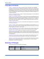
About This Manual . . . . . . . . . . . . . . . . . . . . . . . . . . . . . . . . . . . . . . . . . . . . . . . . . . . . . . . . . . . . . . . . . xv
Overview of Contents . . . . . . . . . . . . . . . . . . . . . . . . . . . . . . . . . . . . . . . . . . . . . . . . . . . . . . . . . . . . . xvi
Summary of Changes . . . . . . . . . . . . . . . . . . . . . . . . . . . . . . . . . . . . . . . . . . . . . . . . . . . . . . . . . . . . xvi
Comments and Suggestions . . . . . . . . . . . . . . . . . . . . . . . . . . . . . . . . . . . . . . . . . . . . . . . . . . . . . . .xvii
Conventions Used in This Manual . . . . . . . . . . . . . . . . . . . . . . . . . . . . . . . . . . . . . . . . . . . . . . . . . . .xvii
1
Preparation and Installation. . . . . . . . . . . . . . . . . . . . . . . . . . . . . . . . . . . . . . . . . . . . . . . . . . . . . . . . 1
Introduction . . . . . . . . . . . . . . . . . . . . . . . . . . . . . . . . . . . . . . . . . . . . . . . . . . . . . . . . . . . . . . . . . . . . .
PrPMC800 Description . . . . . . . . . . . . . . . . . . . . . . . . . . . . . . . . . . . . . . . . . . . . . . . . . . . . . . . . . . . . .
Monarch and Non-Monarch PrPMCs . . . . . . . . . . . . . . . . . . . . . . . . . . . . . . . . . . . . . . . . . . . . . .
Carrier Board Requirements . . . . . . . . . . . . . . . . . . . . . . . . . . . . . . . . . . . . . . . . . . . . . . . . . . . . .
System Enclosure . . . . . . . . . . . . . . . . . . . . . . . . . . . . . . . . . . . . . . . . . . . . . . . . . . . . . . . . . . . . .
Overview of Start-Up Procedures . . . . . . . . . . . . . . . . . . . . . . . . . . . . . . . . . . . . . . . . . . . . . . . . . . . .
Unpacking the Hardware . . . . . . . . . . . . . . . . . . . . . . . . . . . . . . . . . . . . . . . . . . . . . . . . . . . . . . . . . . .
Preparing the Hardware . . . . . . . . . . . . . . . . . . . . . . . . . . . . . . . . . . . . . . . . . . . . . . . . . . . . . . . . . . . .
PrPMC800 Configuration . . . . . . . . . . . . . . . . . . . . . . . . . . . . . . . . . . . . . . . . . . . . . . . . . . . . . . . .
Harrier Power-Up Configuration Header . . . . . . . . . . . . . . . . . . . . . . . . . . . . . . . . . . . . . . . . . . . .
Installation . . . . . . . . . . . . . . . . . . . . . . . . . . . . . . . . . . . . . . . . . . . . . . . . . . . . . . . . . . . . . . . . . . . . . .
ESD Precautions . . . . . . . . . . . . . . . . . . . . . . . . . . . . . . . . . . . . . . . . . . . . . . . . . . . . . . . . . . . . . .
Installation of PrPMC800 on a VME or CompactPCI Board . . . . . . . . . . . . . . . . . . . . . . . . . . . . .
2
1
1
2
2
2
3
3
4
4
4
6
6
6
Operating Instructions . . . . . . . . . . . . . . . . . . . . . . . . . . . . . . . . . . . . . . . . . . . . . . . . . . . . . . . . . . . . 9
Introduction . . . . . . . . . . . . . . . . . . . . . . . . . . . . . . . . . . . . . . . . . . . . . . . . . . . . . . . . . . . . . . . . . . . . . 9
Applying Power . . . . . . . . . . . . . . . . . . . . . . . . . . . . . . . . . . . . . . . . . . . . . . . . . . . . . . . . . . . . . . . . . . 9
Status LEDs and Port Connections . . . . . . . . . . . . . . . . . . . . . . . . . . . . . . . . . . . . . . . . . . . . . . . . . . 10
Status Indicators . . . . . . . . . . . . . . . . . . . . . . . . . . . . . . . . . . . . . . . . . . . . . . . . . . . . . . . . . . . . . 10
Debug Serial Port . . . . . . . . . . . . . . . . . . . . . . . . . . . . . . . . . . . . . . . . . . . . . . . . . . . . . . . . . . . . 11
Ethernet Port Adapter Cable . . . . . . . . . . . . . . . . . . . . . . . . . . . . . . . . . . . . . . . . . . . . . . . . . . . . 11
3
Functional Description . . . . . . . . . . . . . . . . . . . . . . . . . . . . . . . . . . . . . . . . . . . . . . . . . . . . . . . . . . . 13
Introduction . . . . . . . . . . . . . . . . . . . . . . . . . . . . . . . . . . . . . . . . . . . . . . . . . . . . . . . . . . . . . . . . . . . .
Features . . . . . . . . . . . . . . . . . . . . . . . . . . . . . . . . . . . . . . . . . . . . . . . . . . . . . . . . . . . . . . . . . . . . . . .
General Description . . . . . . . . . . . . . . . . . . . . . . . . . . . . . . . . . . . . . . . . . . . . . . . . . . . . . . . . . . . . . .
Block Diagram . . . . . . . . . . . . . . . . . . . . . . . . . . . . . . . . . . . . . . . . . . . . . . . . . . . . . . . . . . . . . . . . . .
Processor . . . . . . . . . . . . . . . . . . . . . . . . . . . . . . . . . . . . . . . . . . . . . . . . . . . . . . . . . . . . . . . . . .
L2 Cache . . . . . . . . . . . . . . . . . . . . . . . . . . . . . . . . . . . . . . . . . . . . . . . . . . . . . . . . . . . . . . . . . . .
Harrier System Memory Controller / PCI Host Bridge ASIC . . . . . . . . . . . . . . . . . . . . . . . . . . . .
PrPMC8005E Processor PMC Module Installation and Use (6806800A42B)
13
13
14
15
16
16
16
vii
Contents
Harrier Power-Up Configuration . . . . . . . . . . . . . . . . . . . . . . . . . . . . . . . . . . . . . . . . . . . . . .
Arbitration . . . . . . . . . . . . . . . . . . . . . . . . . . . . . . . . . . . . . . . . . . . . . . . . . . . . . . . . . . . . . . . . . .
Flash Memory . . . . . . . . . . . . . . . . . . . . . . . . . . . . . . . . . . . . . . . . . . . . . . . . . . . . . . . . . . . . . . .
Onboard Bank A Flash . . . . . . . . . . . . . . . . . . . . . . . . . . . . . . . . . . . . . . . . . . . . . . . . . . . . .
Optional Bank B Flash . . . . . . . . . . . . . . . . . . . . . . . . . . . . . . . . . . . . . . . . . . . . . . . . . . . . .
ECC Memory . . . . . . . . . . . . . . . . . . . . . . . . . . . . . . . . . . . . . . . . . . . . . . . . . . . . . . . . . . . . . . . .
Onboard SDRAM . . . . . . . . . . . . . . . . . . . . . . . . . . . . . . . . . . . . . . . . . . . . . . . . . . . . . . . . .
SROM . . . . . . . . . . . . . . . . . . . . . . . . . . . . . . . . . . . . . . . . . . . . . . . . . . . . . . . . . . . . . . . . . . . . .
10BaseT/100BaseTX Ethernet Channel . . . . . . . . . . . . . . . . . . . . . . . . . . . . . . . . . . . . . . . . . . .
Miscellaneous Control and Status . . . . . . . . . . . . . . . . . . . . . . . . . . . . . . . . . . . . . . . . . . . . . . . .
Timers . . . . . . . . . . . . . . . . . . . . . . . . . . . . . . . . . . . . . . . . . . . . . . . . . . . . . . . . . . . . . . . . . . . . .
32-Bit Timers . . . . . . . . . . . . . . . . . . . . . . . . . . . . . . . . . . . . . . . . . . . . . . . . . . . . . . . . . . . . .
Watchdog Timers . . . . . . . . . . . . . . . . . . . . . . . . . . . . . . . . . . . . . . . . . . . . . . . . . . . . . . . . .
Interrupt Routing and Generation . . . . . . . . . . . . . . . . . . . . . . . . . . . . . . . . . . . . . . . . . . . . . . . .
Asynchronous Serial Port . . . . . . . . . . . . . . . . . . . . . . . . . . . . . . . . . . . . . . . . . . . . . . . . . . . . . .
Clock Generator . . . . . . . . . . . . . . . . . . . . . . . . . . . . . . . . . . . . . . . . . . . . . . . . . . . . . . . . . . . . .
PrPMC800 Power Supplies . . . . . . . . . . . . . . . . . . . . . . . . . . . . . . . . . . . . . . . . . . . . . . . . . . . . .
Module Reset Logic . . . . . . . . . . . . . . . . . . . . . . . . . . . . . . . . . . . . . . . . . . . . . . . . . . . . . . . . . . .
PCI Interface . . . . . . . . . . . . . . . . . . . . . . . . . . . . . . . . . . . . . . . . . . . . . . . . . . . . . . . . . . . . . . . .
PRESENT# Signal . . . . . . . . . . . . . . . . . . . . . . . . . . . . . . . . . . . . . . . . . . . . . . . . . . . . . . . .
MONARCH# Signal . . . . . . . . . . . . . . . . . . . . . . . . . . . . . . . . . . . . . . . . . . . . . . . . . . . . . . . .
INTA#-INTD# Signals . . . . . . . . . . . . . . . . . . . . . . . . . . . . . . . . . . . . . . . . . . . . . . . . . . . . . .
IDSELB, REQB#, and GNTB# Signals . . . . . . . . . . . . . . . . . . . . . . . . . . . . . . . . . . . . . . . . .
M66EN Signal . . . . . . . . . . . . . . . . . . . . . . . . . . . . . . . . . . . . . . . . . . . . . . . . . . . . . . . . . . . .
RESETOUT_L Signal . . . . . . . . . . . . . . . . . . . . . . . . . . . . . . . . . . . . . . . . . . . . . . . . . . . . . .
EREADY Signal . . . . . . . . . . . . . . . . . . . . . . . . . . . . . . . . . . . . . . . . . . . . . . . . . . . . . . . . . .
PCI Signaling Voltage Level . . . . . . . . . . . . . . . . . . . . . . . . . . . . . . . . . . . . . . . . . . . . . . . . .
Debug Header . . . . . . . . . . . . . . . . . . . . . . . . . . . . . . . . . . . . . . . . . . . . . . . . . . . . . . . . . . . . . . .
ABORT# and RESET# Signals . . . . . . . . . . . . . . . . . . . . . . . . . . . . . . . . . . . . . . . . . . . . . . .
Harrier Power-Up Configuration Header . . . . . . . . . . . . . . . . . . . . . . . . . . . . . . . . . . . . . . . . . . .
On-Board LEDs . . . . . . . . . . . . . . . . . . . . . . . . . . . . . . . . . . . . . . . . . . . . . . . . . . . . . . . . . . . . . .
Memory Maps . . . . . . . . . . . . . . . . . . . . . . . . . . . . . . . . . . . . . . . . . . . . . . . . . . . . . . . . . . . . . . .
4
Connector Pin Assignments . . . . . . . . . . . . . . . . . . . . . . . . . . . . . . . . . . . . . . . . . . . . . . . . . . . . . . 29
Introduction . . . . . . . . . . . . . . . . . . . . . . . . . . . . . . . . . . . . . . . . . . . . . . . . . . . . . . . . . . . . . . . . . . . .
PCI Mezzanine Card (PMC) Connectors . . . . . . . . . . . . . . . . . . . . . . . . . . . . . . . . . . . . . . . . . . . . . .
Signal Description for P14 . . . . . . . . . . . . . . . . . . . . . . . . . . . . . . . . . . . . . . . . . . . . . . . . . . . . . .
Ethernet Adapter Connector . . . . . . . . . . . . . . . . . . . . . . . . . . . . . . . . . . . . . . . . . . . . . . . . . . . . . . .
Debug Header . . . . . . . . . . . . . . . . . . . . . . . . . . . . . . . . . . . . . . . . . . . . . . . . . . . . . . . . . . . . . . . . . .
Signal Description for J1 . . . . . . . . . . . . . . . . . . . . . . . . . . . . . . . . . . . . . . . . . . . . . . . . . . . . . . .
Harrier Power-Up Configuration Header . . . . . . . . . . . . . . . . . . . . . . . . . . . . . . . . . . . . . . . . . . . . . .
Debug Serial Port Cable . . . . . . . . . . . . . . . . . . . . . . . . . . . . . . . . . . . . . . . . . . . . . . . . . . . . . . . . . .
5
17
19
19
20
20
20
20
20
21
21
21
21
22
22
22
22
23
23
24
25
25
25
25
25
25
25
26
26
26
26
26
27
29
29
33
35
36
37
37
38
PPCBug . . . . . . . . . . . . . . . . . . . . . . . . . . . . . . . . . . . . . . . . . . . . . . . . . . . . . . . . . . . . . . . . . . . . . . . 39
Overview . . . . . . . . . . . . . . . . . . . . . . . . . . . . . . . . . . . . . . . . . . . . . . . . . . . . . . . . . . . . . . . . . . . . . . 39
viii
PrPMC8005E Processor PMC Module Installation and Use (6806800A42B)
Contents
PPCBug Basics . . . . . . . . . . . . . . . . . . . . . . . . . . . . . . . . . . . . . . . . . . . . . . . . . . . . . . . . . . . . . . . . .
Memory Requirements . . . . . . . . . . . . . . . . . . . . . . . . . . . . . . . . . . . . . . . . . . . . . . . . . . . . . . . .
PPCBug Implementation . . . . . . . . . . . . . . . . . . . . . . . . . . . . . . . . . . . . . . . . . . . . . . . . . . . . . . .
MPU, Hardware, and Firmware Initialization . . . . . . . . . . . . . . . . . . . . . . . . . . . . . . . . . . . . . . . . . . .
Using PPCBug . . . . . . . . . . . . . . . . . . . . . . . . . . . . . . . . . . . . . . . . . . . . . . . . . . . . . . . . . . . . . . . . . .
Debugger Commands . . . . . . . . . . . . . . . . . . . . . . . . . . . . . . . . . . . . . . . . . . . . . . . . . . . . . . . . .
Diagnostic Tests . . . . . . . . . . . . . . . . . . . . . . . . . . . . . . . . . . . . . . . . . . . . . . . . . . . . . . . . . . . . .
6
Modifying the Environment . . . . . . . . . . . . . . . . . . . . . . . . . . . . . . . . . . . . . . . . . . . . . . . . . . . . . . . 49
Overview . . . . . . . . . . . . . . . . . . . . . . . . . . . . . . . . . . . . . . . . . . . . . . . . . . . . . . . . . . . . . . . . . . . . . .
CNFG – Configure Board Information Block . . . . . . . . . . . . . . . . . . . . . . . . . . . . . . . . . . . . . . . . . . .
ENV – Set Environment . . . . . . . . . . . . . . . . . . . . . . . . . . . . . . . . . . . . . . . . . . . . . . . . . . . . . . . . . . .
Configuring the PPCBug Parameters . . . . . . . . . . . . . . . . . . . . . . . . . . . . . . . . . . . . . . . . . . . . .
A
57
57
57
58
58
Thermal Validation . . . . . . . . . . . . . . . . . . . . . . . . . . . . . . . . . . . . . . . . . . . . . . . . . . . . . . . . . . . . . . 59
Overview . . . . . . . . . . . . . . . . . . . . . . . . . . . . . . . . . . . . . . . . . . . . . . . . . . . . . . . . . . . . . . . . . . . . . .
Thermally Significant Components . . . . . . . . . . . . . . . . . . . . . . . . . . . . . . . . . . . . . . . . . . . . . . .
Component Temperature Measurement . . . . . . . . . . . . . . . . . . . . . . . . . . . . . . . . . . . . . . . . . . . . . .
Preparation . . . . . . . . . . . . . . . . . . . . . . . . . . . . . . . . . . . . . . . . . . . . . . . . . . . . . . . . . . . . . . . . .
Measuring Junction Temperature . . . . . . . . . . . . . . . . . . . . . . . . . . . . . . . . . . . . . . . . . . . . . . . .
Measuring Case Temperature . . . . . . . . . . . . . . . . . . . . . . . . . . . . . . . . . . . . . . . . . . . . . . . . . . .
Measuring Local Air Temperature . . . . . . . . . . . . . . . . . . . . . . . . . . . . . . . . . . . . . . . . . . . . . . . .
C
49
49
50
50
Specifications . . . . . . . . . . . . . . . . . . . . . . . . . . . . . . . . . . . . . . . . . . . . . . . . . . . . . . . . . . . . . . . . . . 57
Specifications . . . . . . . . . . . . . . . . . . . . . . . . . . . . . . . . . . . . . . . . . . . . . . . . . . . . . . . . . . . . . . . . . . .
Mechanical Characteristics . . . . . . . . . . . . . . . . . . . . . . . . . . . . . . . . . . . . . . . . . . . . . . . . . . . . .
Electrical Characteristics . . . . . . . . . . . . . . . . . . . . . . . . . . . . . . . . . . . . . . . . . . . . . . . . . . . . . . .
Environmental Characteristics . . . . . . . . . . . . . . . . . . . . . . . . . . . . . . . . . . . . . . . . . . . . . . . . . . .
EMC Compliance . . . . . . . . . . . . . . . . . . . . . . . . . . . . . . . . . . . . . . . . . . . . . . . . . . . . . . . . . . . . . . . .
B
39
40
40
40
42
42
45
59
59
62
62
63
63
63
Related Documentation . . . . . . . . . . . . . . . . . . . . . . . . . . . . . . . . . . . . . . . . . . . . . . . . . . . . . . . . . . 65
Emerson Network Power - Embedded Computing Documents . . . . . . . . . . . . . . . . . . . . . . . . . . . . . 65
Manufacturers’ Documents . . . . . . . . . . . . . . . . . . . . . . . . . . . . . . . . . . . . . . . . . . . . . . . . . . . . . . . . 66
Related Specifications . . . . . . . . . . . . . . . . . . . . . . . . . . . . . . . . . . . . . . . . . . . . . . . . . . . . . . . . . . . . 67
PrPMC8005E Processor PMC Module Installation and Use (6806800A42B)
ix
Contents
x
PrPMC8005E Processor PMC Module Installation and Use (6806800A42B)
List of Tables
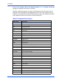
Table 1-1. PrPMC8005E Models/Configurations . . . . . . . . . . . . . . . . . . . . . . . . . . . . . . . . . . . . . . . . xv
Table 1-1. Start-Up Overview . . . . . . . . . . . . . . . . . . . . . . . . . . . . . . . . . . . . . . . . . . . . . . . . . . . . . . . 3
Table 1-2. J2 Harrier Power-Up Configuration Header Pin Assignments . . . . . . . . . . . . . . . . . . . . . . 4
Table 3-3. PrPMC800 Features . . . . . . . . . . . . . . . . . . . . . . . . . . . . . . . . . . . . . . . . . . . . . . . . . . . . . 13
Table 3-4. Harrier Power-Up Configuration Settings . . . . . . . . . . . . . . . . . . . . . . . . . . . . . . . . . . . . . 17
Table 3-5. PPC to PCI Clock Ratios . . . . . . . . . . . . . . . . . . . . . . . . . . . . . . . . . . . . . . . . . . . . . . . . . 22
Table 3-6. Reset Source Functions . . . . . . . . . . . . . . . . . . . . . . . . . . . . . . . . . . . . . . . . . . . . . . . . . . 23
Table 4-7. PMC Connector P11 Pin Assignments . . . . . . . . . . . . . . . . . . . . . . . . . . . . . . . . . . . . . . . 29
Table 4-8. PMC Connector P12 Pin Assignments . . . . . . . . . . . . . . . . . . . . . . . . . . . . . . . . . . . . . . . 30
Table 4-9. PMC Connector P13 Pin Assignments . . . . . . . . . . . . . . . . . . . . . . . . . . . . . . . . . . . . . . . 31
Table 4-10. PMC Connector P14 Pin Assignments . . . . . . . . . . . . . . . . . . . . . . . . . . . . . . . . . . . . . . 32
Table 4-11. J3 Ethernet Adapter Connector Pin Assignments . . . . . . . . . . . . . . . . . . . . . . . . . . . . . 35
Table 4-12. J1 Debug Header Pin Assignments . . . . . . . . . . . . . . . . . . . . . . . . . . . . . . . . . . . . . . . . 36
Table 4-13. J2 Harrier Power-Up Configuration Header Pin Assignments . . . . . . . . . . . . . . . . . . . . 37
Table 4-14. PrPMC Cable-001 Termination . . . . . . . . . . . . . . . . . . . . . . . . . . . . . . . . . . . . . . . . . . . . 38
Table 5-1. Debugger Commands . . . . . . . . . . . . . . . . . . . . . . . . . . . . . . . . . . . . . . . . . . . . . . . . . . . . 42
Table 5-2. Diagnostic Test Groups . . . . . . . . . . . . . . . . . . . . . . . . . . . . . . . . . . . . . . . . . . . . . . . . . . 46
Table A-3. Power Requirements for PrPMC800 . . . . . . . . . . . . . . . . . . . . . . . . . . . . . . . . . . . . . . . . 57
Table A-4. PrPMC800 Environmental Specifications . . . . . . . . . . . . . . . . . . . . . . . . . . . . . . . . . . . . . 58
Table B-5. Thermally Significant Components . . . . . . . . . . . . . . . . . . . . . . . . . . . . . . . . . . . . . . . . . 60
Table C-6. Emerson Network Power - Embedded Computing Publications . . . . . . . . . . . . . . . . . . . 65
Table C-7. Manufacturers’ Documents . . . . . . . . . . . . . . . . . . . . . . . . . . . . . . . . . . . . . . . . . . . . . . . 66
Table C-8. Related Specifications . . . . . . . . . . . . . . . . . . . . . . . . . . . . . . . . . . . . . . . . . . . . . . . . . . . 67
PrPMC8005E Processor PMC Module Installation and Use (6806800A42B)
xi
List of Tables
xii
PrPMC8005E Processor PMC Module Installation and Use (6806800A42B)
List of Figures
Figure 1-1.
Figure 1-2.
Figure 2-3.
Figure 3-4.
Figure 3-5.
Figure B-1.
Figure B-2.
Figure B-3.
Figure B-4.
PrPMC800 Headers, Connectors and Components . . . . . . . . . . . . . . . . . . . . . . . . . . . . . 5
Installing a PrPMC800 on a VMEmodule . . . . . . . . . . . . . . . . . . . . . . . . . . . . . . . . . . . . . 7
PrPMC800 Debug Serial Port Configuration . . . . . . . . . . . . . . . . . . . . . . . . . . . . . . . . . . 11
PrPMC800 Block Diagram . . . . . . . . . . . . . . . . . . . . . . . . . . . . . . . . . . . . . . . . . . . . . . . 15
PrPMC800 Reset Block Diagram . . . . . . . . . . . . . . . . . . . . . . . . . . . . . . . . . . . . . . . . . . 24
Thermally Significant Components (Primary Side) . . . . . . . . . . . . . . . . . . . . . . . . . . . . . 61
Thermally Significant Components (Secondary Side) . . . . . . . . . . . . . . . . . . . . . . . . . . 62
Measuring Local Air Temperature . . . . . . . . . . . . . . . . . . . . . . . . . . . . . . . . . . . . . . . . . . 63
Mounting a Thermocouple Under a Heatsink . . . . . . . . . . . . . . . . . . . . . . . . . . . . . . . . . 64
PrPMC8005E Processor PMC Module Installation and Use (6806800A42B)
xiii
List of Figures
xiv
PrPMC8005E Processor PMC Module Installation and Use (6806800A42B)
About This Manual
The PrPMC8005E Processor PMC Module Installation and Use provides information for
installation and configuration of the PrPMC8005E board, including jumper settings and
installation procedures. It also includes descriptions of various components’ functions,
connector pinout information, and a general description of the PPCBug firmware used with the
board. Hereafter, the PrPMC8005E will be referred to as the PrPMC800.
Information in this manual applies to Emerson boards that are compatible with the PowerPC™
instruction set architecture and that use PPCBug as their resident debugger program. The
majority of these boards, including most Processor PMC, VME, CompactPCI® and ATX form
factors, are equipped with PPCBug.
This document is limited to the installation and use instructions. For programming information,
refer to the Harrier ASIC Programmer’s Reference Guide and the PrPMC800 Processor PMC
Module Programmer’s Reference Guide.
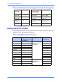
The following table lists the various model numbers and configurations for the PrPMC800. Note
that some of the models listed below qualify as Class B devices. If you require a Class B device,
contact your Emerson sales representative for specific models and configurations that meet
those requirements.
Table 1-1. PrPMC8005E Models/Configurations
Model Number
Processor /
Speed
L2
Cache
Memory
Ethernet
PCI Bus
Speed
PrPMC8005E-1261
MPC7410/
450 MHz
2MB
256MB
Front
33 MHz
PrPMC8005E-1259
MPC7410/
450 MHz
2MB
128MB
Rear
33 MHz
PrPMC8005E-1269
MPC7410/
450 MHz
2MB
256MB
Rear
33 MHz
PrPMC8005E-2261
MPC7410/
450 MHz
2MB
256MB
None
66 MHz
Capable
PrPMC800C5E-2261
MPC7410/
450 MHz
2MB
256MB
None
66 MHz
Capable
PrPMC8005E-2271
MPC7410/
450 MHz
2MB
512MB
None
66 MHz
Capable
PrPMC8005E Processor PMC Module Installation and Use (6806800A42B)
xv
About This Manual
Overview of Contents
Chapter 1, Preparation and Installation, provides a general description of the PrPMC800
including a summary of the basic features and architecture. It also includes a brief discussion
of the monarch and non-monarch use of this board, and the carrier board requirements when
the PrPMC800 is being used as a monarch. The remainder of the chapter includes an overview
of the start-up procedures, general information on unpacking and hardware preparation, and
installation instructions.
Chapter 2, Operating Instructions, contains a section on applying power, a brief description of
status LEDs and debug serial ports.
Chapter 3, Functional Description, provides a list of the main features of the PrPMC800. It also
provides a general description of the board, a block diagram, and subsections on all of the major
components on the board, including configuration settings for the Harrier ASIC. In addition, it
also describes various key functions such as arbitration, setting flash memory, memory size
settings and system registers.
Chapter 4, Connector Pin Assignments, includes tables of pin assignments for all connectors
and headers on the board.
Chapter 5, PPCBug, includes a general discussion of PPCBug, the initialization process and
steps, and a brief summary of the use of PPCBug with a list of current commands. A list of the
current Diagnostic Test Groups is also included.
Chapter 6, Modifying the Environment, provides a general overview of how to change various
parameters within PPCBug firmware. It discusses two main commands: ENV and CNFG.
Appendix A, Specifications, provides basic mechanical, electrical and environmental
specifications for the PrPMC800, as well as a section on Thermal Validation offering information
on thermally significant components and an overview of how to measure various junction and
case temperatures.
Appendix B, Thermal Validation, provides systems integrators with information which can be
used to conduct thermal evaluations of the board in their specific system configuration.
Appendix C, Related Documentation, provides a list of other Emerson Embedded Computing
related documents, applicable Manufacturer’s (vendor) documents, and a list of related
specifications.Comments and Suggestions
Summary of Changes
See the table below for manual revisions and changes.
xvi
Part Number
Date
Description
6806800A42B
September 2008
Update document to Emerson style (logo, copyright,
trademarks, etc.)
PrPMC8005E Processor PMC Module Installation and Use (6806800A42B)
About This Manual
Comments and Suggestions
We welcome and appreciate your comments on our documentation. We want to know what you
think about our manuals and how we can make them better.
Mail comments to us by filling out the following online form:
http://www.emersonnetworkpowerembeddedcomputing.com/ > Contact Us > Online Form
In “Area of Interest” select “Technical Documentation”. Be sure to include the title, part number,
and revision of the manual and tell us how you used it.
Conventions Used in This Manual
The following typographical conventions are used in this document:
bold
is used for user input that you type just as it appears. Bold is also used for commands,
options and arguments to commands, and names of programs, directories and files.
italic
is used for names of variables to which you assign values. Italic is also used for
comments in screen displays and examples, and to introduce new terms.
courier
is used for system output (for example, screen displays, reports), examples, and
system prompts.
<Enter>, <Return> or <CR>
<CR> represents the carriage return or Enter key.
CTRL
represents the Control key. Execute control characters by pressing the Ctrl key and the
letter simultaneously, for example, Ctrl-d.
|
separates two or more items from which to choose (one only)
[]
encloses an optional item that may not occur at all, or may occur once.
{}
encloses an optional item that may not occur at all, or may occur one or more times.
A character precedes a data or address parameter to specify the numeric format, as follows (if
not specified, the format is hexadecimal):
$
dollar
0x
Zero-x
a hexadecimal character.
PrPMC8005E Processor PMC Module Installation and Use (6806800A42B)
xvii
About This Manual
%
percent
a binary number.
&
ampersand
a decimal number.
Data and address sizes are defined as follows:
A byte is eight bits, numbered 0 through 7, with bit 0 being the least significant.
A half-word is 16 bits, numbered 0 through 15, with bit 0 being the least significant.
A word is 32 bits, numbered 0 through 31, with bit 0 being the least significant.
The MPU on the board is programmed to big-endian byte ordering. Any attempt to use littleendian byte ordering will immediately render the debugger unusable.
Note: All references to processor bus support via the Harrier ASIC relate
specifically to the MPC60x-class bus mode. They do not imply support of any
other PowerPC-architecture bus mode.
xviii PrPMC8005E Processor PMC Module Installation and Use (6806800A42B)
1
Preparation and Installation
1
Introduction
This chapter provides a brief description of the PrPMC8005E Processor PMC Module and
instructions for preparing and installing the hardware.
In this manual, the name PrPMC800 refers to all models of the PrPMC8005E series boards,
unless otherwise specified. These are add-on modules intended for use with any host carrier
board that accepts a PMC or PrPMC module.
PrPMC800 Description
The PrPMC800 is a single-width, standard-length and standard-height Processor PCI
Mezzanine Card (PrPMC) board. It is compatible with the PowerPlus III architecture and
consists of an MPC7410 processor and the Harrier PCI-Host bridge/system memory controller
ASIC. The PrPMC800 features 2MB of L2 cache, 32MB of flash memory (a second bank of
flash can be located on the baseboard and accessed through the PMC P14 connector), one
bank of SDRAM (128MB to 256MB) onboard, a 10BaseT/100BaseTX Ethernet channel based
on the Intel 82559ER/82551IT device and an RS-232 transceiver providing debug capabilities
through one of the Harrier UART channels.
Four 64-pin PMC connectors on the PrPMC800 are used to connect the PrPMC800 to the host
board. One right-angle 20-pin connector located on the primary side of the PrPMC800 provides
an interface to the asynchronous serial port and the processor JTAG/COP port, along with the
RESET# and ABORT# signals used for debug support. The serial port and JTAG/COP
interfaces, along with the ABORT_L signal, are also routed to the PMC P14 connector for host
board access.
Connectivity to the Ethernet channel is provided either by a front panel connector or by rear I/O
via the P14 connector. The build option determines the connection method. Models of this
board configured for Ethernet routing via the Pn4 do not have a front bezel.
The PrPMC800 module can operate as a monarch (master) for the baseboard, or as a slave
processor PMC, depending on the state of the MONARCH# signal from the PMC P12
connector. When configured as the monarch, the PrPMC800 enumerates the PCI bus, and
monitors and services the four PCI interrupts. If configured to operate in the non-monarch
mode, the PrPMC800 module does not enumerate the bus or service interrupts, but it may
generate a PCI interrupt. The following section describes these modes of operation in greater
detail.
PrPMC8005E Processor PMC Module Installation and Use (6806800A42B)
1
1 Preparation and Installation
Monarch and Non-Monarch PrPMCs
The traditional concept of host/master and slave/target processors changes with the inception
of the PrPMC because of the arbiter and clock source. Traditionally located on the host board,
these functions are not part of the PrPMC800. The VITA 32 specification defines the terms
monarch and non-monarch to refer to these two modes of operation for PrPMCs. A monarch
PrPMC is defined as the main PCI bus PrPMC (or CPU) that performs PCI bus enumeration at
power-up or reset and acts as the PCI interrupt handler. The non-monarch is a slave/target
processor that does not perform bus enumeration and does not service PCI interrupts but may
generate a PCI interrupt to the host processor.
A system may have one monarch PrPMC800 and/or one or more non-monarch PrPMC800s,
creating a loosely coupled multiprocessing system. A PrPMC800 operating as a monarch may
be mated to a carrier board with slave processors, PCI, and other I/O devices. A PrPMC800
operating as a non-monarch may be installed on a carrier with a host processor and other PCI
devices, such as an CPCI-6065 board. PPCBug does not support all of the operating
characteristics of a PrPMC800 operating as a non-monarch. Consequently, another operating
system, such as a Real-Time Operating System, may be required.
The PrPMC800 firmware PPCBug is configured to operate as either a monarch or non-monarch
by reading the state of the MONARCH# pin on the PrPMC800. This pin is either grounded or
left open on the carrier board to enable the desired mode of operation. Refer to the MONARCH#
signal explanation on page 25 of this manual for more information.
Carrier Board Requirements
A carrier board must provide the standard PCI interface, including +3.3V and +5V power (the
PrPMC800 only requires +3.3V), PCI address/control, a PCI clock, and two PCI arbiter
REQ/GNT pairs (refer to the VITA-32-199x specification for more information). The carrier
board must also ground the MONARCH# pin to enable the monarch operating mode. Leaving
the MONARCH# pin open enables the non-monarch mode. Additionally, board models
PrPMC8005E-2261 and PrPMC8005E -2271 may be configured for 66 MHz PCI operation. To
enable this mode, the M66EN pin must be pulled up on the baseboard.
System Enclosure
The system enclosure requirements are determined by the configuration and architecture of the
baseboard (either VME, CompactPCI, or custom). Only a single slot is necessary for both the
baseboard and the attached PrPMC800 in a VME or CompactPCI chassis.
2
PrPMC8005E Processor PMC Module Installation and Use (6806800A42B)
1 Preparation and Installation
Overview of Start-Up Procedures
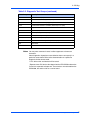
The following table lists the things you need to do before you can use this board and tells where
to find the information you need to perform each step. Be sure to read this entire chapter,
including all Cautions and Warnings, before you begin.
Table 1-1. Start-Up Overview
What you need to do ...
Refer to ...
On page ...
Unpack the hardware.
Unpacking the PrPMC800 Hardware
3
Make any settings or adjustments
on the PrPMC800 module.
Preparing the PrPMC800 Hardware
4
PrPMC800 Configuration Considerations
4
Prepare any other optional
devices or equipment you will be
using.
For more information on optional devices and
equipment, refer to the documentation
provided with that equipment.
Install the PrPMC800 on the
baseboard.
Installation of a PrPMC800 on a VME or
CompactPCI board
6
Connect any other optional
devices or equipment you will be
using.
Connector Pin Assignments
29
Power up the system.
Status Indicators
10
You may also wish to obtain the PPCBug
Diagnostics Manual, listed in Appendix C,
Related Documentation.
65
Examine the environmental
parameters and make any
changes needed.
ENV - Set Environment
50
You may also wish to obtain the PPCBug
Firmware Package User’s Manual, listed in
Appendix C, Related Documentation.
65
Program the PrPMC800 module
and PMCs as needed for your
applications.
Preparing the PrPMC800 Hardware
4
You may also wish to obtain the PrPMC800
Processor PMC Module Programmer’s
Reference Guide, listed in Appendix C,
Related Documentation.
65
For more information on optional devices and
equipment, refer to the documentation
provided with that equipment.
Unpacking the Hardware
Note
If the shipping carton(s) is/are damaged upon receipt, request that the carrier's
agent be present during the unpacking and inspection of the equipment.
Unpack the equipment from the shipping carton(s). Refer to the packing list(s) and verify that
all items are present. Save the packing material for storing and reshipping of equipment.
Avoid touching areas of integrated circuitry; static discharge can damage these
circuits.
Caution
PrPMC8005E Processor PMC Module Installation and Use (6806800A42B)
3
1 Preparation and Installation
Preparing the Hardware
To produce the desired configuration and ensure proper operation of the PrPMC800, you may
need to carry out certain modifications before and after installing the modules.
The following paragraphs discuss the preparation of the PrPMC800 hardware components prior
to installing them into a chassis and connecting them.
PrPMC800 Configuration
The PrPMC800 provides software control over most options. By setting bits in control registers,
after installing the PrPMC800 in a system, you can modify its configuration. Refer to Table 1-2
on page 4 for information on the Harrier Power-Up Configuration header, which provides access
for configuration control. The PrPMC800 control registers are described in detail in the
PrPMC800 Processor PMC Module Programmer's Reference Guide and the Harrier ASIC
Programmer’s Reference Guide as listed in Appendix C, Related Documentation.
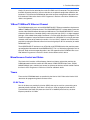
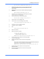
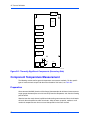
Figure 1-1 on page 5 shows the placement of headers, connectors, and components on the
PrPMC800. The PrPMC800 was factory tested and is shipped with the configurations described
in the following sections. It contains a factory-installed debug monitor, PPCBug, which operates
with those factory settings.
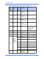
Harrier Power-Up Configuration Header
A 2mm, 16-pin low profile header located on side 1 of the PrPMC800 provides the means to
change some of the Harrier power-up configuration settings. The pin assignments for this
header, along with the power-up setting with the jumper on or off, are as follows (boards are
shipped with all jumpers off):
Table 1-2. J2 Harrier Power-Up Configuration Header Pin Assignments
4
J2
Jumper On
Jumper Off
1-2
PUST0 = 0
Harrier PUST Bit 0 in GCSR Register.
PUST0 = 1
3-4
PUST1 = 0
Harrier PUST Bit 1 in GCSR Register
PUST1 = 1
5-6
PUST2 = 0
Harrier PUST Bit 2 in GCSR Register
PUST2 = 1
7-8
PUST3 = 0
Harrier PUST Bit 2 in GCSR Register
PUST3 = 1
9-10
Hold off Configuration Space access
Configuration Space
access enabled
11-12
Processor held in reset at power-up
Processor enabled at
power-up
13-14
Class Code set for I2O Controller”
Class Code set for
“Bridge Device”
15-16
Xport 1uses normal data byte ordering
Xport 1 uses Hawk
data byte ordering
PrPMC8005E Processor PMC Module Installation and Use (6806800A42B)
1 Preparation and Installation
J3
15
1
U2
U6
2
1
16
2
1
J2
15
L3
J1
U10
19 20
U1
L5
U9
T1
U8
U5
U4
U7
1
P11
2
1
2
P12
63
1
64
2
63
1
64
2
P13
63
64
P14
63
64
Figure 1-1. PrPMC800 Headers, Connectors and Components
PrPMC8005E Processor PMC Module Installation and Use (6806800A42B)
5
1 Preparation and Installation
Installation
The following instructions tell how to install the PrPMC800 on a typical VME or CompactPCI
single board computer. The PrPMC800 can also be installed on an ATX form factor carrier
board that is equipped with industry standard PMC slots.
ESD Precautions
Use ESD
Wrist Strap
Emerson strongly recommends that you use an antistatic wrist strap and a
conductive foam pad when installing or upgrading a system. Electronic
components, such as disk drives, computer boards, and memory modules,
can be extremely sensitive to ESD. After removing the component from the
system or its protective wrapper, place the component flat on a grounded,
static-free surface (and, in the case of a board, component side up). Do not
slide the component over any surface.
If an ESD station is not available, you can avoid damage resulting from ESD by wearing an
antistatic wrist strap (available at electronics stores) that is attached to an active electrical
ground. Note that a system chassis may not be grounded if it is unplugged.
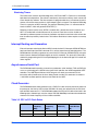
Installation of PrPMC800 on a VME or CompactPCI Board
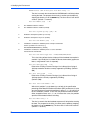
To install a PrPMC800 mezzanine on an VMEmodule or CompactPCI board, refer to Figure 1-2
and perform the following steps:
1. Attach an ESD strap to your wrist. Attach the other end of the ESD strap to an electrical
ground. (Note that the system chassis may not be grounded if it is unplugged) The ESD
strap must be secured to your wrist and to ground throughout the procedure.
2.
Perform an operating system shutdown. Turn the AC or DC power off and remove the
AC cord or DC power lines from the system. Remove the chassis or system cover(s) as
necessary to gain access to the VMEmodule or CompactPCI board.
!
Inserting or removing modules with power applied may result in damage to
module components.
Caution
3.
Carefully remove the VMEmodule or CompactPCI board from its card slot and place it
on a clean and adequately protected working surface (preferably an ESD mat) with the
backplane connectors facing you.
Avoid touching areas of integrated circuitry; static discharge can damage
circuits.
Caution
4.
6
Place the PrPMC800 mezzanine module on top of the VMEmodule, or CompactPCI
board, with the four PMC connectors on the PrPMC800 aligned with the four
corresponding connectors on the baseboard. Connectors P11, P12, P13, and P14 at the
bottom edge of the PrPMC800 should connect smoothly with the corresponding
connectors on the VMEmodule or CompactPCI board.
PrPMC8005E Processor PMC Module Installation and Use (6806800A42B)
1 Preparation and Installation
Figure 1-2. Installing a PrPMC800 on a VMEmodule
5.
Align the standoffs on the PrPMC800 mezzanine with the VMEmodule or CompactPCI
board. Install the Phillips-head screws through the holes in the baseboard and the
spacers. Tighten the screws.
6.
Install the VME or CompactPCI assembly in its proper card slot. Ensure the module is
seated properly in the backplane connectors. Do not damage or bend connector pins.
7.
Replace the chassis or system cover(s) and connect the system to the AC or DC power
source. Turn the equipment power on.
PrPMC8005E Processor PMC Module Installation and Use (6806800A42B)
7
1 Preparation and Installation
8
PrPMC8005E Processor PMC Module Installation and Use (6806800A42B)
2
Operating Instructions
2
Introduction
This chapter provides information about powering up the PrPMC800 system, and functionality
of the status indicators, and I/O ports on the PrPMC800 module.
Applying Power
After you have verified that all necessary hardware preparation has been done, that all
connections have been made correctly, and that the installation is complete, you can power up
the system. The MPU, hardware and firmware initialization process is performed by the
PPCBug firmware at power-up or system reset. The firmware initializes the devices on the
PrPMC800 module in preparation for booting the operating system.
The firmware, PPCBug, is shipped from the factory with an appropriate set of defaults. In most
cases there is no need to modify the firmware configuration before you boot the operating
system. However, if you choose to do so, refer to Chapter 6, Modifying the Environment for
further information about modifying these defaults.
The following flowchart shows the basic initialization process that takes place during PrPMC800
system start-up.
For further information on PPCBug, refer to Chapter 5, PPCBug, or to the PPCBug
documentation listed in Appendix C, Related Documentation.
PrPMC8005E Processor PMC Module Installation and Use (6806800A42B)
9
2 Operating Instructions
STARTUP
INITIALIZATION
POST
Power-up/reset initialization
Initialize devices on the PrPMC800
module/system
Power On Self Test diagnostics
BOOTING
Firmware-configured boot mechanism,
if so configured. Default is no boot.
MONITOR
Interactive, command-driven on-line PowerPC
debugger, when terminal connected.
Status LEDs and Port Connections
The PrPMC800’s status indicators (LEDs), Debug Serial port and Ethernet Port adapter cable
are described in the following subsections.
Status Indicators
There are two LED (light-emitting diode) status indicators located on the secondary side of
thePrPMC800, BDFL and CPU.
BDFL
The yellow fail LED is lit when the Harrier Board fail bit (BDFL) in the Miscellaneous Control and
Status register is active (software controlled). This LED is illuminated at reset and then turned
off after PPCBug has successfully completed initialization.
CPU
The green CPU LED is lit when the DBB# (Data Bus Busy) signal line on the processor bus is
active (hardware controlled).
10
PrPMC8005E Processor PMC Module Installation and Use (6806800A42B)
2 Operating Instructions
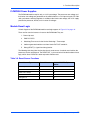
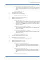
Debug Serial Port
A three-wire debug serial RS-232 port (TXD, RXD, GND) is available on the 2mm, 20-pin rightangle header (J1) located on the primary side of the PrPMC800. Refer to Figure 2-3 for pin
definitions. An optional J1-to-DB9 adapter cable is available from Emerson. Contact your local
Emerson Sales Office or Distributor for more information or to order cable part number: PrPMCCABLE-001. The pinout description for this cable is defined in Debug Serial Port Cable on page
38.
The debug port may be used for connecting a terminal to the PrPMC800 to serve as the
firmware console for the factory installed debugger, PPCBug. The port is configured as follows:
❏
8 bits per character
❏
1 stop bit per character
❏
Parity disabled (no parity)
❏
Baud rate = 9600 baud (default baud rate at power-up)
After power-up, the baud rate of the debug port can be reconfigured by using the debugger’s
Port Format (PF) command. Refer to Chapter 5, PPCBug and Chapter 6, Modifying the
Environment for information about PPCBug.
SOUT0
19
SIN0
20
14
Harrier
PrPMC800
Debug
Header J1
Figure 2-3. PrPMC800 Debug Serial Port Configuration
Ethernet Port Adapter Cable
An Ethernet port adapter cable is available for those models with front panel Ethernet. The
cable provides the capability to adapt the low profile Ethernet connector (J3) to a standard RJ45
receptacle. Contact your local Emerson Sales Office to order cable part number: PRPMCCable-003.
PrPMC8005E Processor PMC Module Installation and Use (6806800A42B)
11
2 Operating Instructions
12
PrPMC8005E Processor PMC Module Installation and Use (6806800A42B)
3
Functional Description
3
Introduction
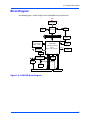
This chapter describes the PrPMC800 Processor PMC Module on a block diagram level. The
General Description provides an overview of the PrPMC800, followed by a detailed description
of several blocks of circuitry. Figure 3-4 on page 15 shows a block diagram of the overall board
architecture.
Detailed descriptions of other PrPMC800 blocks, including programmable registers in the ASIC
and peripheral chips, can be found in the PrPMC800 Processor PMC Module Programmer’s
Reference Guide and the Harrier ASIC Programmer’s Reference Guide, listed in Appendix C,
Related Documentation. Refer to those documents for a more comprehensive set of functional
descriptions.
Features
The following table summarizes the features of the PrPMC800 processor module.
Table 3-3. PrPMC800 Features
Feature
Description
Processor
Single MPC7410 processor
Core frequencies of 450Mhz for MPC7410
Bus clock frequency of 100 MHz.
Address and data bus parity
L2 Cache
Backside L2 Cache using pipeline burst-mode SRAMS:
2MB for the MPC7410
Data bus parity
Flash Memory
Bank A: 32MB soldered on-board using two 128 Mbit devices.
Bank B: Second bank of flash can be located on host board and
accessed through the PMC P14 connector.
SDRAM
Double-Bit-Error detect, Single-Bit-Error correct across 72 bits
Single bank of 16-bit wide devices onboard provide 128MB to
256MB SDRAM.
Memory Controller
Harrier’s SMC (System Memory Controller).
PCI Host Bridge
Harrier’s PHB (PCI Host Bridge).
Interrupt Controller
Harrier’s MPIC (Multi-Processor Interrupt Controller).
PCI Interface
32/64-bit Data
33 MHz minimum, 66 MHz capable on certain models
+3.3V/+5V universal signaling compatible interface
P11, P12, P13 and P14 PMC connectors
Address/data parity per PCI specification
PrPMC8005E Processor PMC Module Installation and Use (6806800A42B)
13
3 Functional Description
Table 3-3. PrPMC800 Features (continued)
Feature
Description
Ethernet Interface
10BaseT/100BaseTX interface based on the Intel
82559ER/82551IT device
AT93C46 SROM for 82559ER/82551IT configuration
SROM
Two 8K byte dual-address I2C serial EEPROM devices for Vital
Product Data, user configuration data
One 256 byte standard I2C serial EEPROM for memory SPD
Debug Support
Two 16550-compatible async serial ports (in Harrier) with RS-232
interface
Processor JTAG/COP Interface
RESET and ABORT signals
Signals routed to 2mm header and PMC connector P14
Input Power
Requirements
3.3V + 5%
Form Factor
Single-width, standard-length PMC (74mm x 149mm) with 10mm
board-to-board stacking height.
Standard (3.5mm) side 2 height
General Description
The PrPMC800 is a Emerson processor PMC module compatible with the PowerPlus III
architecture. It consists of an MPC7410 processor and:
❏
L2 backside cache
❏
Harrier System Memory Controller/PCI Host Bridge ASIC
❏
32MB of flash memory
❏
128MB TO 256MB of ECC-protected SDRAM on board with memory expansion
capability
❏
10BaseT/100BaseTX Ethernet controller
❏
Debug serial port
The PrPMC800 module interfaces to the host board PCI bus via the PMC P11, P12 and P13
connectors. These provide a 64-bit PCI interface (that is, 33 MHz/66 MHz capable) between the
host board and the PrPMC800. The PrPMC module draws +3.3V through the PMC connectors.
The onboard Processor Core Power Supply derives the core voltage from the +3.3V power. The
clock generator derives all of the required onboard clocks from the PCI clock input on P11.
The PrPMC800 module has a 2mm header onboard to support module debug operations. This
header provides the interface to the debug serial RS-232 port and an interface to the processor
JTAG/COP port.
The PrPMC800 module can function as a system controller (monarch mode) for the host board
or as a slave processor (non-monarch) PMC, depending on the state of the MONARCH# signal
from the PMC connector. When configured as the monarch, the PrPMC800’s PPCBug
enumerates the PCI bus as well as monitor and service the four PCI interrupts.
14
PrPMC8005E Processor PMC Module Installation and Use (6806800A42B)
3 Functional Description
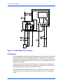
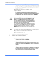
Block Diagram
The following figure is a block diagram of the PrPMC800’s overall architecture
+3.3V
Processor Core
Power Supply
Debug
Header
Processor
L2 Cache
2MB
MPC7410
MPC60xProcessor
ProcessorBus
Bus
PPC60x
RS-232
TXCVR
Bank A
Onboard SDRAM
128MB - 256MB
OSC
1.84 MHZ
Harrier ASIC
PCI Host Bridge (PHB)
+3.3V
+2.5V Core
Power Supply
System
Memory Controller (SMC)
Xport 0
Flash Bank A
32MB
Clock
Generator
Front
Connector
PMC P11/P12/P13 Connectors
SROM
AT24Cxx
Flash Bank B (Xport 1)
82559ER/82551IT
10/100 Ethernet
32/64-bit PCI Bus
SROM
AT93C46
PMC P14 Connector
Figure 3-4. PrPMC800 Block Diagram
PrPMC8005E Processor PMC Module Installation and Use (6806800A42B)
15
3 Functional Description
Processor
The PrPMC800 board can be ordered with 450 MHz MPC7410-class, low-power/low care
voltage processor chip.
L2 Cache
The PrPMC800 utilizes a backside L2 cache structure via the MPC7410 processor chip family.
The L2 cache is implemented with an on-chip, 2-way set-associative tag memory and external
direct-mapped synchronous SRAMs for data storage. The external SRAMs are accessed
through a dedicated 72-bit wide (64 bits of data and 8 bits of parity) L2 cache port. The
MPC7410 processor can support up to 2MB. The L2 cache can operate in copyback or writethrough modes and supports system cache coherency through snooping. Data parity
generation and checking can be disabled by programming the processor’s L2 cache control
register accordingly. The MPC7410 processor also supports direct mapping of the SRAM
memory, in conjunction with normal L2 cache operation. In this mode, a portion of the SRAM
memory space may be mapped to appear as a private memory space in the memory map.
Refer to the processor data sheet for additional information.
The L2 cache data SRAM for the PrPMC800 is implemented using two 128K x 36 or 256K x 36
synchronous pipelined burst SRAMs providing a total of 2MB of L2 cache.
Harrier System Memory Controller / PCI Host Bridge ASIC
The Harrier ASIC provides the bridge function between the PPC60x bus, the system memory,
and the PCI Local Bus. The Harrier ASIC incorporates the following key features:
❏
100 MHz PowerPC-compatible bus interface
❏
SDRAM interface supporting up to eight banks of 512MB each, with ECC
❏
32/64-bit REV2.1 compliant PCI bus interface capable of running up to 66 MHz
❏
Single channel DMA controller
❏
Message passing unit supporting I2O and generic functions
❏
Two internal 16550-type UARTs
❏
Two I2C bus master interfaces
❏
MPIC compliant interrupt controller
❏
Four Xport channels for interfacing to flash or other external registers/devices
Refer to the Harrier Programmer’s Guide for additional information and programming details.
16
PrPMC8005E Processor PMC Module Installation and Use (6806800A42B)
3 Functional Description
Harrier Power-Up Configuration
The Harrier ASIC XAD30-XAD0 pins provide configuration information for Harrier at power-up
reset time. The following table lists the default power-up reset state of these pins for the
PrPMC800 module. The Select Option column indicates whether the power-up setting can be
changed by jumper, or if the setting is fixed and cannot be changed. The Default Power-Up
Setting column indicates the default values for the standard PrPMC800 product. Default
settings for jumper options indicate power-up values with jumpers not installed.
Table 3-4. Harrier Power-Up Configuration Settings
Harrier
XAD
Bus
Signal
Select
Option
Default
PowerUp
Setting
Function/
Register Bit
Description
XAD[30]
Jumper J2
pins 15-16
1
Hawk data mode
XCSR.XPGC.HDM
Enable/Disable (1/0) Hawk
16-bit data ordering mode for
Xports configured for Hawk
addressing mode. Xport 1
(flash bank B) is configured
for Hawk compatibility mode.
If disabled, use Harrier byte
ordering mode.
XAD[29]
Fixed
0
UART clock select
Select external clock source
for UART.
XAD[28]
Jumper J2
pins 9-10
0
PCI slave
configuration holdoff
XCSR.BPCS.CSH
Enable/disable (1/0)
configuration space hold off.
If enabled, accesses to the
PCI configuration space from
another PCI master results
in a disconnect retry. Local
PrPMC800 software must
clear this register bit to
enable access after inbound
address and attribute fields
have been set.
XAD[27]
Fixed
0
PCI slave
configuration mask
XCSR.BPCS.CSM
All of Harrier’s PCI
configuration registers are
visible from PCI space.
XAD[26]
Jumper J2
pins11-12
0
Processor holdoff
XCSR.BXCS
Enable/disable (1/0)
processor hold off at powerup. If enabled, processor is
held in reset.
XAD[25]
Fixed
0
SDRAM external
register
XCSR.SDTC.SDER
There are no external buffers
in series with the BAx, RAx,
WE, RAS or CAS signals.
XAD[24]
Fixed
1
Response to
unmapped addressonly cycles
XCSR.GCSR.AOAO
Harrier responds to
unmapped address only
cycles.
PrPMC8005E Processor PMC Module Installation and Use (6806800A42B)
17
3 Functional Description
Table 3-4. Harrier Power-Up Configuration Settings (continued)
Harrier
XAD
Bus
Signal
Select
Option
Default
PowerUp
Setting
Function/
Register Bit
Description
XAD[23]
Jumper J2
pins 7-8
1
Generic power up
status bit 3
XCSR.GCSR.PUST
3
Software readable header bit
3
XAD[22]
Jumper J2
pins 5-6
1
Generic power up
status bit 2
XCSR.GCSR.PUST
2
Software readable header bit
2
XAD[21]
Jumper J2
pins 3-4
1
Generic power up
status bit 1
XCSR.GCSR.PUST
1
Software readable header bit
1
XAD[20]
Jumper J2
pins 1-2
1
Generic power up
status bit 0
XCSR.GCSR.PUST
0
Software readable header bit
0
XAD[19]
Jumper J2
pins 13-14
0
I2O IOP agent
Set PCI Configuration
register CLAS to present
class code for “bridge
device” (0) or “I2O
Controller” (1)
XAD[18]
Fixed
0
Internal PCI arbiter
Disable internal PCI arbiter
XAD[17]
Fixed
1
Internal processor
arbiter
Enable internal Processor
arbiter
XAD
[16:15]
Fixed
00
XCSR register
group base address
Set XCSR register group
base address to $FEFF0000
000
reserved
001
3:2
Set PPC-to-PCI clock ratio to
3:2
010
2:1
Set PPC-to-PCI clock ratio to
2:1
011
5:2
Set PPC-to-PCI clock ratio to
5:2
100
1:1
Set PPC-to-PCI clock ratio to
1:1
101
reserved
110
3:1
111
reserved
01
Xport channel 0
data width
XCSR.XPAT0.DW
XAD
[14-12]
XAD
[11:10]
18
On board
logic sets
ratio
depending
on state of
M66EN
Fixed
Set PPC-to-PCI clock ratio to
3:1
Set flash bank A to 16-bit
width
PrPMC8005E Processor PMC Module Installation and Use (6806800A42B)
3 Functional Description
Table 3-4. Harrier Power-Up Configuration Settings (continued)
Harrier
XAD
Bus
Signal
Select
Option
Default
PowerUp
Setting
Function/
Register Bit
Description
XAD[9]
BankB_SE
L
x
Xport channel 0
reset vector source
Enable/Disable (1/0) Xport
channel 0 (flash bank A) as
reset vector source,
depending on state of
baseboard jumper.
XAD
[8:7]
Fixed
11
Xport channel 1
data width
XCSR.XPAT1.DW
Set Xport channel 1 (flash
bank B) to 16-bit width,
Hawk addressing mode.
XAD[6]
Fixed
1
Xport channel 1
reset vector source
Enable Xport channel 1
(flash bank B) as reset
vector source if Xport
channel 0 is disabled.
XAD
[5:4]
Fixed
xx
Xport channel 2
data width
XCSR.XPAT2.DW
Unused.
XAD[3]
Fixed
0
Xport channel 2
reset vector source
Disable Xport channel 2 as
Reset Vector source
XAD
[2:1]
Fixed
xx
Xport channel 3
data width
XCSR.XPAT2.DW
Unused.
XAD[0]
Fixed
0
Xport Channel 3
Reset Vector Source
Disable Xport channel 3 as
Reset Vector source
Arbitration
The Harrier ASIC contains arbiters for the PPC bus (60x bus mode only) and the PCI bus. The
PPC arbiter is used to arbitrate between the processor and the Harrier PPC bus master for
ownership of the PPC bus. The processor is connected to the Harrier arbiter
CPU0_REQ/CPU0_GNT signal pair (XARB3/XARB0).
The Harrier PCI bus arbiter is disabled in the standard board configuration. Per the VITA-32
199x Processor PMC Standard, the PCI bus arbitration must be provided by the baseboard.
Flash Memory
The PrPMC800 supports two banks of flash memory. Bank A is onboard flash, while bank B is
optional flash located on the host board and accessed through the PMC P14 connector.
PrPMC8005E Processor PMC Module Installation and Use (6806800A42B)
19
3 Functional Description
Onboard Bank A Flash
The PrPMC800 contains one bank of 32MB of flash memory on Xport 0 configured for 16-bit
mode. Bank A consists of two Intel StrataFlash (28F128J3D) +3.3 volt devices configured to
operate in 8-bit mode. These Intel StrataFlash devices support page read mode operations with
an 8-byte page size per device.
Optional Bank B Flash
The signal interface for the Harrier Xport 1, configured to operate in Hawk 16-bit address/data
mode, is routed to the PMC P14 connector to support an optional 16-bit flash bank B on the
baseboard. The address multiplexing of the Hawk mode can address up to 512MB, but device
loading may restrict this size to less than that. The reset vector may be sourced by either bank
A or bank B depending on the state of the Harrier Xport reset vector control bits
(RVEN0/RVEN1). When the RVEN0 bit is set, address range $FFF00000-$FFFFFFFF maps to
bank A. When RVEN0 bit is cleared and the RVEN1 bit is set, the address range $FFF00000$FFFFFFFF maps to bank B. The default state uses bank A for the reset vector. Bank B may
be selected by connecting the BANKB_SEL pin on P14 to +3.3V.
Xport 1 may be configured to operate in the normal data byte ordering mode where the data
alternates every byte instead of every forth byte (Hawk data mode). The data ordering mode is
controlled by one of the onboard jumpers.
ECC Memory
The PrPMC800 supports onboard ECC SDRAM configured as explained below.
Onboard SDRAM
The PrPMC800 onboard ECC SDRAM memory, bank A, is configured as one bank of nine 8bit wide, +3.3V SDRAM devices in 54-pin TSOPII packages. The total onboard memory size
can be 64MB, 128MB, 256MB, or 512MB depending on the memory type used. The SDRAM
memory is controlled by the Harrier ASIC which provides single-bit error correction and doublebit error detection. ECC is calculated over 72-bits. Refer to the Harrier ASIC Programmer’s
Reference Guide for additional information and programming details. The SDRAM memory bus
operates at the same speed as the processor bus.
SROM
The PrPMC800 module contains two 8Kb serial EEPROM devices (AT24C64A) and one 256
byte serial EEPROM device (AT24C02) onboard. One 8Kb serial EEPROM provides for Vital
Product Data (VPD) storage of the module hardware configuration, and the other 8Kb device
provides storage for user configuration data. The contents of the devices are accessed by
providing a two-byte address with the same device ID, instead of the standard one-byte address
as used in the 256 byte devices. The 256 byte device provides for Serial Presence Detect (SPD)
memory configuration information. The Serial EEPROM’s are accessed through I2C port 0 in
the Harrier ASIC. Refer to Appendix B of the PrPMC800 Processor PMC Module Programmer’s
Reference Guide for information on the contents of the VPD and SPD.
20
PrPMC8005E Processor PMC Module Installation and Use (6806800A42B)
3 Functional Description
Harrier I2C port 0 is also routed to pins on the P14 PMC user I/O connector. The connection to
the PMC connector provides a means to interface to an optional configuration SROM on the
baseboard. This allows the PrPMC800 to determine hardware configuration information from
the baseboard. Refer to the Harrier ASIC Programmer’s Reference Guide for SROM device
address assignments.
10BaseT/100BaseTX Ethernet Channel
The PrPMC800 module uses an Intel GD82559ER/82551IT Ethernet controller to implement a
10BaseT/100BaseTX Ethernet channel. The GD82559ER/82551IT is a lower power, lower cost
version of the GD82559 without the wake-on-LAN features. The GD82559ER/82551IT consists
of both the Media Access Controller (MAC) and the physical layer (PHY) in a single integrated
package. A Pulse H0013 low profile transformer is used to supply the external magnetics. The
module will support a front panel Ethernet connection via a low profile PC card style connector
mounted at the front of the module (on models -12x1 and -52x1). Optional rear I/O Ethernet is
provided by routing the Ethernet transmit and receive signal pairs to P14 connector (on model
PrPMC880-1279).
The 82559ER/82551IT interfaces to an AT93C46 serial EEPROM device that provides powerup configuration information for the 82559ER/82551IT. This is a 1Kb device organized as 64 16bit words. Refer to the corresponding table in the VPD appendix of the PrPMC800 Processor
PMC Module Programmer’s Reference Guide, for the contents of this device.
Miscellaneous Control and Status
The Harrier ASIC contains a Miscellaneous Control and Status register that provides the
PrPMC800 module with the module fail LED control, PrPMC EREADY# pin status, PrPMC
MONARCH# pin status, module reset control, and processor timebase enable control. Refer to
the Harrier ASIC Programmer’s Reference Guide for additional details.
Timers
Timers on the PrPMC800 board are provided by the Harrier ASIC. Refer to the Harrier ASIC
documents for programming details on these timers.
32-Bit Timers
Four 32-bit timers are provided by Harrier (MPIC) that may be used for system timing or to
generate periodic interrupts. Each timer is driven by a divide-by-eight prescaler which is
synchronized to the Power PC processor clock. For a 100 MHz processor bus, the timer
frequency would be 12.5 MHz.
PrPMC8005E Processor PMC Module Installation and Use (6806800A42B)
21
3 Functional Description
Watchdog Timers
The Harrier ASIC contains two Watchdog timers, WDT0 and WDT1. Each timer is functionally
equivalent but independent. These timers continuously decrement until they reach a count of 0
or are reloaded by software. The time-out period is programmable from 1 microsecond up to 32
minutes. If the timer count reaches 0, a timer output signal is asserted. The output of Watchdog
Timer 0 is routed to an MPIC interrupt. The output of Watchdog Timer 1 is connected to the
Harrier AUXRST, which will generate RESETOUT_L.
Following a Harrier device reset, WDT0 is enabled with a default time-out of 8 seconds and
WDT 1is enabled with a default time-out of 16 seconds. Each timer must be disabled or
reloaded by software to prevent a time-out. Software may reload a new timer value or force the
timer to reload a previously loaded value. To disable or load/reload a timer requires a two step
process.
Interrupt Routing and Generation
External interrupts routed to the Harrier MPIC include the four PCI interrupts INTA#-INTD#, four
host board interrupts from PMC connector P14, and the output from the watchdog timers. The
PrPMC800 has the ability to generate any one of the PCI interrupts INTA#-INTD# by using the
Harrier Generic Outbound Doorbell register or the I2O controller. The desired PCI interrupt is
selected by programming the PCI Interrupt Mapping bits in the Harrier Bridge PCI Control and
Status register.
Asynchronous Serial Port
The PrPMC800 module provides a two-wire asynchronous serial interface (TXD and RXD) for
use as a serial debug port. UART0 in the Harrier ASIC provides the 16550 compatible UART
controller. The UART0 port SIN0 and SOUT0 signals are wired to an external RS-232
transceiver which interfaces to the 2mm debug header and the P14 connector. An onboard
1.8432 MHz oscillator provides the baud rate clock for the UART.
Clock Generator
The PrPMC800 module clock generator uses a Z9972 PLL clock driver to provide the clocks for
the processor, the Harrier ASIC and the SDRAMs. All clocks are referenced to the PCI clock
input on PMC connector P11. The PrPMC800 supports the PPC-to-PCI clock ratios listed in the
following table. Onboard logic uses the state of the PMC M66EN pin to determine whether the
maximum PCI clock frequency will be 33 MHz or 66 MHz.
Table 3-5. PPC to PCI Clock Ratios
22
M66EN Pin
PPC Clock
Frequency
(MHz)
PCI Clock
Frequency
(MHz)
Ratio
(PPC:PCI)
Harrier PCI
Clock Divisor
(N)
Low
100
33.33
3:1
12
High
100
66.67
3:2
6
PrPMC8005E Processor PMC Module Installation and Use (6806800A42B)
3 Functional Description
PrPMC800 Power Supplies
The PrPMC800 module requires only a +3.3V input voltage. The processor core voltage and
the Harrier core voltage are generated on the module from the +3.3V input using the LTC1702
dual synchronous switching regulator. In addition to the Harrier core voltage, the +2.5V supply
provides the processor, Harrier, and L2 cache I/O voltages.
Module Reset Logic
A block diagram of the PrPMC800 module reset logic appears in Figure 3-5 on page 24.
There are five standard sources of reset on the PrPMC800. They are:
1. Power-Up reset
2.
PMC PCI RST#
3.
Watchdog Timer reset via the Harrier Watchdog 1 Timer output
4.
Software generated module reset from Harrier RSTOUT control bit
5.
Debug RESET_L signal from debug header
The following table describes the function of each reset source. A module reset includes the
processor, Harrier and Ethernet. The RESETOUT_L pin must be tied into the baseboard reset
logic, which drives PCIRST# in order to produce module reset.
Table 3-6. Reset Source Functions
Reset Source Type
Module Reset
PrPMC RESETOUT_L
Active
Power-Up Reset
x
x
PMC PCI RST#
x
WDT1 Timer Output
x
SW Reset
x
Debug Reset
x
PrPMC8005E Processor PMC Module Installation and Use (6806800A42B)
23
SRESET_L
TRST_L
HRESET_L
SRST0_L
WDT1TO_L
HRST0_L
RWSRESEST_L
J1-11
P14-13
RWCPUTSRT_L
J1-4
P14-7
RWCPURST_L
P14-14
J1-13
REQ64 LOGIC
RST_L
AUXRST_L
PCIRST_L
ABTSW_L
ABORT_L
J1-18
P14-42
MCSR.RSTOUT
RSTSW_L
DEBUGRST_L
J1-17
P12-13
RSTOUT_L
PURST_L
Power Up
Reset
(140ms)
Harrier ASIC
RESETOUT_L
MPC7410-Class Processor
P12-60
3 Functional Description
Figure 3-5. PrPMC800 Reset Block Diagram
PCI Interface
The PrPMC800 module contains four EIA-E700 AAAB connectors that provide a 32/64-bit PCI
interface to an IEEE P1386.1 PMC compliant baseboard. Connectors P11-P13 provide the
32/64-bit 66 MHz capable PCI interface while P14 provides an I/O path from the module to the
baseboard. Signals routed to P14 include the I2C bus, the RS-232 debug port, the processor
JTAG/COP and the Xport 1.
PCI bus pullup resistors required by the PCI Revision 2.1 Specification (for motherboards),
including 64-bit expansion signals, must be supplied by the baseboard. This is required if the
PrPMC800 is operating as a monarch or non-monarch module.
The following special function processor PMC pins, as defined by the draft Processor PMC
Standard VITA-32-199x, are implemented on the PrPMC800 as described in the following
sections.
24
PrPMC8005E Processor PMC Module Installation and Use (6806800A42B)
3 Functional Description
PRESENT# Signal
The PRESENT# signal on the PrPMC800 module is grounded to indicate to the baseboard that
the module is installed.
MONARCH# Signal
The MONARCH# input signal allows the baseboard to enable the monarch system controller
features on the PrPMC800 module. The PrPMC800 will pull up the MONARCH# signal. If the
baseboard grounds this pin, the PrPMC800 module will operate as a monarch (master) and
provide system initialization and PCI interrupt handling. If the baseboard leaves the
MONARCH# pin floating, the PrPMC800 will operate as a non-monarch (slave).
INTA#-INTD# Signals
The four PCI interrupt signals are routed to MPIC external interrupt inputs so that they can be
monitored by the processor when the PrPMC800 is operating in the monarch mode. The
PrPMC800 can generate an interrupt to the host board processor on any one PCI interrupt
INTA#-INTD# by activating the PCI interrupt in the Harrier message passing unit. Refer to the
interrupt section of the Harrier ASIC Programmer’s Reference Guide for interrupt assignments.
IDSELB, REQB#, and GNTB# Signals
The PrPMC800 module uses the processor PMC second PCI agent signals IDSELB, REQB#
and GNTB# for the IDSEL, REQ# and GNT# signals of the GD82559ER/82551IT Ethernet chip.
IDSELB has a weak onboard pulldown and GNTB# has a weak onboard pullup so the module
operates properly on baseboards that do not support a second PCI agent.
M66EN Signal
The no-Ethernet versions (PrPMC8005E-2261 and PrPMC8005E-2271) of the module are
designed to operate on a 33 MHz or 66 MHz PCI bus, depending on the state of the M66EN pin
provided by the baseboard. The module will monitor the state of the M66EN pin and set the
multiplier of the on board clock generator at power-up. If the M66EN pin is grounded, the clock
ratio will be 3:1. If M66EN is high, the clock ratio will be set to 3:2.
RESETOUT_L Signal
The PrPMC RESETOUT_L output signal (P12-60) provides a means for the PrPMC800 to reset
the baseboard which in turn can reset the PrPMC800. The active low RESETOUT_L signal is
generated whenever the PrPMC800 power-up reset, Watchdog Timer 1 reset, debug reset, or
a software generated module reset via the Harrier RESET OUT bit is active. The PMC PCI reset
input signal will not generate RESETOUT_L. Refer to Figure 3-5 for a diagram of the module
reset logic.
EREADY Signal
The Processor PMC PCI bus Enumeration Ready (EREADY) signal is connected to the Harrier
EREADY pin. Harrier can drive this open drain signal and monitor its state using the Harrier
EREADY and EREADYS status bits. This pin is asserted low by Harrier at power-up and must
be deasserted by software control.
PrPMC8005E Processor PMC Module Installation and Use (6806800A42B)
25
3 Functional Description
PCI Signaling Voltage Level
The PrPMC800 module is a universal PMC module that will operate with +3.3V or +5V PCI
signaling levels. The Harrier PCI I/O buffers operate at +3.3V output levels and are 5V tolerant
allowing the PCI interface to operate at either voltage level. The one exception is the PCI CLK
input. This is a +3.3V “only” input, which is not +5V tolerant. The PCI clock input signal is a
+3.3V only input.
Debug Header
A 2mm, 20-pin right-angle header located on side one of the PrPMC800 provides the interface
to the async serial port, the processor JTAG/COP port, along with the RESET# and ABORT#
signals. The serial port and JTAG/COP interfaces, along with the ABORT_L signal, are also
routed to the PMC P14 connector for host board access.
ABORT# and RESET# Signals
The debug header provides ABORT# and RESET# inputs for debug purposes. The ABORT#
signal is connected to the Harrier Abort Switch (ABTSW_L) input and generates an MPIC
internal interrupt. The RESET# signal is connected to the Harrier Reset Switch (RSTSW_L)
input that generates a Harrier Reset Out. Each signal is debounced in the Harrier ASIC.
Harrier Power-Up Configuration Header
A 2mm, 16-pin low profile header, locate on side one of the module provides the means to
change some of the Harrier power-up configuration settings. See Table 4-13 on page 37 for
configuration settings controlled by this header. A 2-mm shunt must be installed to change a
setting. The default configuration setting (with the shunt not installed) is also given in Table 4-13.
Refer to Table 4-13 for the header pin assignments as well.
On-Board LEDs
The PrPMC800 module provides two LEDs mounted on side two of the module for status of the
CPU and the board fail pin:
❏
The green CPU LED is lit when the DBB# signal of the processor bus is active
(hardware controlled)
❏
The yellow FAIL LED is lit when the Harrier Board Fail bit (BDFL) in the Miscellaneous
Control and Status register is active (software controlled)
Refer to the Harrier ASIC Programmer’s Reference Guide for details of the Miscellaneous
Control and Status register.
26
PrPMC8005E Processor PMC Module Installation and Use (6806800A42B)
3 Functional Description
Memory Maps
Refer to the PrPMC800 Processor PMC Module Programmer’s Reference Guide for memory
maps of the PrPMC800 processor module. The PrPMC800 is a derivative of the Single Board
Computer (SBC) family compatible with the PowerPlus III architecture. The programming model
presented in the PrPMC800 Programmer’s Reference Guide is based on the PowerPlus III
architecture.
PrPMC8005E Processor PMC Module Installation and Use (6806800A42B)
27
3 Functional Description
28
PrPMC8005E Processor PMC Module Installation and Use (6806800A42B)
4
Connector Pin Assignments
4
Introduction
This chapter provides connector pin assignments for all connectors on the PrPMC800 board.
PCI Mezzanine Card (PMC) Connectors
There are four 64-pin EIA E700 AAAB SMT connectors (P11, P12, P13, and P14) on the
PrPMC800 that provide the 32/64-bit PCI interface and optional I/O interface to the host board.
The P14 connector provides an interface to the bank B flash and I2C bus along with a secondary
interface to the serial port and the JTAG/COP port. The pin assignments are as follows.
Table 4-7. PMC Connector P11 Pin Assignments
P11
1
TCK
-12V (No Connect)
2
3
GND
INTA#
4
5
INTB#
INTC#
6
7
PRESENT#
+5V (No Connect)
8
9
INTD#
No Connect
10
11
GND
No Connect
12
13
CLK
GND
14
15
GND
GNT#
16
17
REQ#
+5V (No Connect)
18
19
VIO
AD31
20
21
AD28
AD27
22
23
AD25
GND
24
25
GND
C/BE3#
26
27
AD22
AD21
28
29
AD19
+5V (No Connect)
30
31
VIO
AD17
32
33
FRAME#
GND
34
35
GND
IRDY#
36
37
DEVSEL#
+5V (No Connect)
38
39
GND
LOCK#
40
41
SDONE#
SBO#
42
PrPMC8005E Processor PMC Module Installation and Use (6806800A42B)
29
4 Connector Pin Assignments
Table 4-7. PMC Connector P11 Pin Assignments (continued)
43
PAR
GND
44
45
VIO
AD15
46
47
AD12
AD11
48
49
AD09
+5V (No Connect)
50
51
GND
C/BE0#
52
53
AD06
AD05
54
55
AD04
GND
56
57
VIO
AD03
58
59
AD02
AD01
60
61
AD00
+5V (No Connect)
62
63
GND
REQ64#
64
Table 4-8. PMC Connector P12 Pin Assignments
P12
30
1
+12V (No Connect)
TRST#
2
3
TMS
TDO
4
5
TDI
GND
6
7
GND
No Connect
8
9
No Connect
No Connect
10
11
MOT_RSVD
+3.3V
12
13
RST#
MOT_RSVD
14
15
+3.3V
MOT_RSVD
16
17
No Connect
GND
18
19
AD30
AD29
20
21
GND
AD26
22
23
AD24
+3.3V
24
25
IDSEL
AD23
26
27
+3.3V
AD20
28
29
AD18
GND
30
31
AD16
C/BE2#
32
33
GND
IDSELB
34
35
TRDY#
+3.3V
36
37
GND
STOP#
38
39
PERR#
GND
40
41
+3.3V
SERR#
42
PrPMC8005E Processor PMC Module Installation and Use (6806800A42B)
4 Connector Pin Assignments
Table 4-8. PMC Connector P12 Pin Assignments (continued)
43
C/BE1#
GND
44
45
AD14
AD13
46
47
M66EN
AD10
48
49
AD08
+3.3V
50
51
AD07
REQB_L
52
53
+3.3V
GNTB_L
54
55
MOT_RSVD
GND
56
57
MOT_RSVD
EREADY
58
59
GND
RESETOUT_L
60
61
ACK64#
+3.3V
62
63
GND
MONARCH#
64
Table 4-9. PMC Connector P13 Pin Assignments
P13
1
Reserved
GND
2
3
GND
C/BE7#
4
5
C/BE6#
C/BE5#
6
7
C/BE4#
GND
8
9
VIO (No Connect)
PAR64
10
11
AD63
AD62
12
13
AD61
GND
14
15
GND
AD60
16
17
AD59
AD58
18
19
AD57
GND
20
21
VIO (No Connect)
AD56
22
23
AD55
AD54
24
25
AD53
GND
26
27
GND
AD52
28
29
AD51
AD50
30
31
AD49
GND
32
33
GND
AD48
34
35
AD47
AD46
36
37
AD45
GND
38
39
VIO (No Connect)
AD44
40
41
AD43
AD42
42
PrPMC8005E Processor PMC Module Installation and Use (6806800A42B)
31
4 Connector Pin Assignments
Table 4-9. PMC Connector P13 Pin Assignments (continued)
43
AD41
GND
44
45
GND
AD40
46
47
AD39
AD38
48
49
AD37
GND
50
51
GND
AD36
52
53
AD35
AD34
54
55
AD33
GND
56
57
VIO (No Connect)
AD32
58
59
Reserved
Reserved
60
61
Reserved
GND
62
63
GND
Reserved
64
Table 4-10. PMC Connector P14 Pin Assignments
P14
32
1
I2CSDA
I2CSCL
2
3
TXD
RXD
4
5
CPUTDI
CPUTDO
6
7
CPUTRST_L
GND
8
9
GND
BANKB_SEL
10
11
CPUTCK
CPUTMS
12
13
SRESET_L
CPURST_L
14
15
CHKSTPO_L
XOE_L
16
17
XUUWE_L
XCS_L
18
19
XUMWE_L
XALE_L
20
21
XAD5
XWAIT_L
22
23
XAD6
GND
24
25
GND
XADR1
26
27
XADR2
XADR3
28
29
XADR4
XADR5
30
31
XADR6
XADR7
32
33
XAD0
XAD1
34
35
XAD2
XAD3
36
37
XAD4
TXP (optional)
38
39
RXP (optional)
TXN (optional)
40
41
RXN (optional)
ABORT_L
42
PrPMC8005E Processor PMC Module Installation and Use (6806800A42B)
4 Connector Pin Assignments
Table 4-10. PMC Connector P14 Pin Assignments (continued)
43
HOSTINT0
HOSTINT1
44
45
HOSTINT2
HOSTINT3
46
47
XAD31
XAD30
48
49
XAD29
XAD28
50
51
XAD27
XAD26
52
53
XAD25
XAD24
54
55
XAD23
GND
56
57
GND
XAD22
58
59
XAD21
XAD20
60
61
XAD19
XAD18
62
63
XAD17
XAD16
64
Signal Description for P14
I2CSDA:
I2C bus serial data
I2CSCL:
I2C bus clock
TXD:
RS-232 serial port transmit data
RXD:
RS-232 serial port receive data
CPUTDI:
Processor RISCwatch TDI
CPUTDO:
Processor RISCwatch TDO
CPUTRST_L:
Processor RISCwatch Test Reset
CPUTCK:
Processor RISCwatch Test Clock
CPUTMS:
Processor RISCwatch Test Mode Select
SRESET_L:
Processor RISCwatch Soft Reset
CPURST_L:
Processor RISCwatch CPU Reset
CHKSTPO_L:
Processor RISCWatch CPU Checkstop Out
BANKB_SEL:
Flash Bank B reset vector select
XOE_L:
Xport Output Enable. Equivalent to FLASHOE_L on
PrPMC750
XUUWE_L:
Xport Upper Byte Write Enable. Equivalent to
FLASHUWE_L on PrPMC750.
XUMWE_L:
Xport Lower Byte Write Enable in 16-bit mode.
Equivalent to FLASHLWE_L on PrPMC750.
XCS1_L
Xport1 Chip Select. Equivalent to FLASHCS_L on
PrPMC750.
XALE_L
Xport Address Latch Enable. Equivalent to
FLASHALE_L on PrPMC750.
XADR_L (7:1)
Xport address lines. Equivalent to RA_FLASH (6:0) on
PrPMC750.
PrPMC8005E Processor PMC Module Installation and Use (6806800A42B)
33
4 Connector Pin Assignments
34
XAD (6:1)
Xport address lines. Equivalent to BA_FLASH1,
BA_FLASH0, and RA_FLASH (11:7) respectively on
PrPMC750.
XAD (31:16)
Xport 16-bit data bus. Equivalent to RD_FLASH (0:15)
on PrPMC750.
XWAIT_L
FLASH port wait state enable
ABORT_L
ABORT interrupt
HOSTINT(0:3)
Host interrupt
TXP/TXN
Ethernet transmit signal pair for optional rear I/O.
These pins are no connects for front I/O Ethernet.
RXP/RXN
Ethernet receive signal pair for optional rear I/O.
These pins are no connects for front I/O Ethernet.
PrPMC8005E Processor PMC Module Installation and Use (6806800A42B)
4 Connector Pin Assignments
Ethernet Adapter Connector
An AMP 15-pin INFOPORT Series III PC card, low profile connector is located on the front edge
of the PrPMC800 to provide a front side interface to the Ethernet channel. An external PC card
RJ45 adapter cable is required to provide a standard RJ45 Ethernet interface. The pin
assignments for this header are as follows.
Table 4-11. J3 Ethernet Adapter Connector Pin Assignments
J3
1
NC
2
NC
3
NC
4
NC
5
TXP
6
TXN
7
RXP
8
RXN
9
LANTERMA
10
LANTERMA
11
LANTERMB
12
LANTERMB
13
NC
14
NC
15
NC
PrPMC8005E Processor PMC Module Installation and Use (6806800A42B)
35
4 Connector Pin Assignments
Debug Header
A 2mm, 20-pin right-angle header located on side one of the PrPMC800 provides the interface
to the async serial port, the processor JTAG/COP port, the PLD JTAG in-system programming
port, along with the RESET# and ABORT# signals. The serial port and JTAG/COP interfaces,
along with the ABORT_L signal, are also routed to the PMC P14 connector for host board
access. The pin assignments for this header are as follows.
Table 4-12. J1 Debug Header Pin Assignments
J1
36
1
CPUTDO
ISPSDO
2
3
CPUTDI
CPUTRST_L
4
5
ISPSDI
PULLUP
6
7
CPUTCK
ISPMODE
8
9
CPUTMS
ISPSCLK
10
11
SRESET_L
DEBUGINT_L
12
13
CPURST_L
GND
14
15
CKSTPO_L
GND
16
17
RESET_L
ABORT_L
18
19
TXD
RXD
20
PrPMC8005E Processor PMC Module Installation and Use (6806800A42B)
4 Connector Pin Assignments
Signal Description for J1
TXD:
RS-232 serial port transmit data
RXD:
RS-232 serial port receive data
CPUTDI:
Processor RISCWatch TDI
CPUTDO:
Processor RISCWatch TDO
CPUTRST_L:
Processor RISCWatch Test Reset
CPUTCK:
Processor RISCWatch Test Clock
CPUTMS:
Processor RISCWatch Test Mode Select
SRESET_L:
Processor RISCWatch Soft Reset
CPURST_L:
Processor RISCWatch CPU Reset
CHKSTPO_L:
Processor RISCWatch CPU Checkstop out
PULLUP
Fused Pullup for RISCWatch probe
ISPSDO:
PLD ISP Serial Data Out
ISPSDI:
PLD ISP Serial Data In
ISPMODE:
PLD ISP Mode
ISPSCLK:
PLD ISP Serial Clock
ABORT_L
ABORT interrupt
DEBUGINT_L
Debug Interrupt input
RESET_L
Debug Reset input
RSVD
Reserved pins. Do not connect any signals to these pins.
Harrier Power-Up Configuration Header
A 2mm, 16-pin low profile header located on side one of the PrPMC800 provides the means to
change some of the Harrier power-up configuration settings. The pin assignments for this
header, along with the power-up setting with the shunt on or off, are as follows.
Table 4-13. J2 Harrier Power-Up Configuration Header Pin Assignments
J2
Shunt On
Shunt Off
1
XAD[20]
termination
GND
2
PUST0 = 0
Harrier PUST Bit 0
in GCSR Register.
PUST0 = 1
3
XAD[21]
termination
GND
4
PUST1 = 0
Harrier PUST Bit 1
in GCSR Register.
PUST1 = 1
5
XAD[22]
termination
GND
6
PUST2 = 0
Harrier PUST Bit 2
in GCSR Register.
PUST2 = 1
PrPMC8005E Processor PMC Module Installation and Use (6806800A42B)
37
4 Connector Pin Assignments
Table 4-13. J2 Harrier Power-Up Configuration Header Pin Assignments
7
XAD[23]
termination
GND
8
PUST3 = 0
Harrier PUST Bit 3
in GCSR Register.
PUST3 = 1
9
XAD[28]
termination
3.3V
10
Hold off Configuration
Space access
Configuration Space
access enabled
1
1
XAD[26]
termination
3.3V
12
Processor held in reset
at power-up
Processor enabled at
power-up
1
3
XAD[19]
termination
3.3V
14
Class Code set for”I2O
Controller”
Class Code set for
“Bridge Device”
1
5
XAD[30]
termination
GND
16
Xport 1uses normal
data byte ordering
Xport 1 uses Hawk
data byte ordering
Debug Serial Port Cable
The following cable pinout information is provided for those using the debug serial port cable in
conjunction with the operation of the PrPMC800.
Table 4-14. PrPMC Cable-001 Termination
38
Signal Name
2mm
20-Receptacle Pin
(TCSD-10-01)
Mating Connector
Mating
Connector Pin
CPUTDO
1
1
CPUTDI
3
.100’x.100x IDC plug
connector, 16-pin
(4616-7001)
CPUTRST_L
4
4
PULLUP
6
6
CPUTCK
7
7
CPUTMS
9
9
SRESET_L
11
11
CPURST_L
13
13
CKSTPO_L
15
15
GND
16
16
GND
14
TXD
19
RXD
20
D-sub plug
connector, 9-pin
(8209-6000)
PrPMC8005E Processor PMC Module Installation and Use (6806800A42B)
3
5
3
2
5
PPCBug
5
Overview
The PPCBug firmware is the layer of software just above the hardware. The firmware provides
the proper initialization for the devices on the PrPMC800 module upon power-up or reset.
This chapter describes the basics of PPCBug and its architecture, describes the monitor
(interactive command portion of the firmware) in detail, and gives information on actually using
the PPCBug debugger and the special commands. A complete list of PPCBug commands
appears at the end of the chapter.
Chapter 6, Modifying the Environment, contains information about the CNFG and ENV
commands, system calls, and other advanced user topics.
For full user information about PPCbug, refer to the PPCBug Firmware Package User’s Manual
and the PPCBug Diagnostics Manual, listed in Appendix C, Related Documentation.
PPCBug Basics
The debug firmware, PPCBug, is a powerful evaluation and debugging tool for systems built
around Emerson microcomputers compatible with the PowerPC instruction set architecture.
Facilities are available for loading and executing user programs under complete operator control
for system evaluation.
PPCBug provides a high degree of functionality, user friendliness, portability, and ease of
maintenance.
It achieves good portability and comprehensibility because it was written entirely in the C
programming language, except where necessary to use assembler functions.
PPCBug includes commands for:
❏
Display and modification of memory
❏
Breakpoint and tracing capabilities
❏
A powerful assembler and disassembler useful for patching programs
❏
A self-test at power-up feature which verifies the integrity of the system
PPCBug consists of three parts:
❏
A command-driven, user-interactive software debugger, described in the PPCBug
Firmware Package User’s Manual. It is hereafter referred to as “the debugger” or
“PPCBug”.
❏
A command-driven diagnostics package for the PrPMC800 hardware, hereafter
referred to as “the diagnostics.” The diagnostics package is described in the PPCBug
Diagnostics Manual.
PrPMC8005E Processor PMC Module Installation and Use (6806800A42B)
39
5 PPCBug
❏
A user interface or debug/diagnostics monitor that accepts commands from the system
console terminal.
When using PPCBug, you operate out of either the debugger directory or the diagnostic
directory.
❏
If you are in the debugger directory, the debugger prompt
PPC7-Bug> is displayed and all of the debugger commands are available.
❏
If you are in the diagnostic directory, the diagnostic prompt
PPC7-Diag> is displayed and all of the diagnostic commands are available, as well as
all of the debugger commands.
Because PPCBug is command-driven, it performs various operations in response to user
commands entered at the keyboard. When you enter a command, PPCBug executes the
command and the prompt reappears. However, if you enter a command that causes execution
of user target code (e.g., GO), control may or may not return to PPCBug, depending on the
outcome of the user program.
Memory Requirements
PPCBug requires a maximum of 768KB of read/write memory (DRAM). The debugger allocates
this space from the top of memory. For example, a system containing 64MB ($04000000) of
read/write memory places the PPCBug memory page at locations $03F40000 to $03FFFFFF.
PPCBug Implementation
PPCBug is written largely in the C programming language, providing benefits of portability and
maintainability. Where necessary, assembly language has been used in the form of separately
compiled program modules containing only assembler code. No mixed-language modules are
used.
Physically, PPCBug is contained in two on-board flash devices that together provide 32MB of
storage. The executable code is checksummed at every power-on or reset firmware entry, and
the result (which includes a precalculated checksum contained in the flash devices), is verified
against the expected checksum.
MPU, Hardware, and Firmware Initialization
The debugger performs the MPU, hardware, and firmware initialization process. This process
occurs each time the PrPMC800 is reset or powered up. The steps below are a high-level
outline; not all of the detailed steps are listed.
1. Sets MPU.MSR to known value.
40
2.
Invalidates the MPU's data/instruction caches.
3.
Clears all segment registers of the MPU.
4.
Clears all block address translation registers of the MPU.
5.
Initializes the MPU-bus-to-PCI-bus bridge device.
PrPMC8005E Processor PMC Module Installation and Use (6806800A42B)
5 PPCBug
6.
Calculates the external bus clock speed of the MPU.
7.
Delays for 750 milliseconds.
8.
Determines the CPU base board type.
9.
Sizes the local read/write memory (i.e., DRAM).
10. Initializes the read/write memory controller. Sets base address of memory to
$00000000.
11. Retrieves the speed of read/write memory.
12. Initializes the read/write memory controller with the speed of read/write memory.
13. Retrieves the speed of read only memory (flash).
14. Initializes the read only memory controller with the speed of read only memory.
15. Enables the MPU's instruction cache.
16. Copies the MPU's exception vector table from $FFF00000 to $00000000.
17. Verifies MPU type.
18. Enables the superscalar feature of the MPU (superscalar processor boards only).
19. Verifies the external bus clock speed of the MPU.
20. Determines the debugger's console/host ports, and initializes the PC16550A.
21. Displays the debugger's copyright message.
22. Displays any hardware initialization errors that may have occurred.
23. Checksums the debugger object, and displays a warning message if the checksum
failed to verify.
24. Displays the amount of local read/write memory found.
25. Verifies the configuration data that is resident in NVRAM, and displays a warning
message if the verification failed.
26. Calculates and displays the MPU clock speed, verifies that the MPU clock speed
matches the configuration data, and displays a warning message if the verification fails.
27. Displays the BUS clock speed, verifies that the BUS clock speed matches the
configuration data, and displays a warning message if the verification fails.
28. Probes PCI bus for supported network devices.
29. Probes PCI bus for supported mass storage devices.
30. Initializes the memory/IO addresses for the supported PCI bus devices.
31. Executes Self-Test, if so configured. (Default is no Self-Test.)
32. Extinguishes the board fail LED, if Self-Test passed, and outputs any warning
messages.
33. Executes boot program, if so configured. (Default is no boot.)
34. Executes the debugger monitor (issues the PPC7-Bug> prompt).
PrPMC8005E Processor PMC Module Installation and Use (6806800A42B)
41
5 PPCBug
Using PPCBug
PPCBug is command-driven; it performs its various operations in response to commands that
you enter at the keyboard. When the PPC7-Bug prompt appears on the screen, the debugger
is ready to accept debugger commands. When the PPC7-Diag prompt appears on the screen,
the debugger is ready to accept diagnostics commands. To switch from one mode to the other,
enter SD.
What you enter is stored in an internal buffer. Execution begins only after you press the Return
or Enter key. This allows you to correct entry errors, if necessary, with the control characters
described in the PPCBug Firmware Package User’s Manual.
After the debugger executes the command, the prompt reappears. However, if the command
causes execution of user target code (for example GO) then control may or may not return to
the debugger, depending on what the user program does. For example, if a breakpoint has been
specified, control returns to the debugger when the breakpoint is encountered during execution
of the user program. Alternately, the user program could return to the debugger by means of
the System Call Handler routine RETURN. For more about this, refer to the GD, GO, and GT
command descriptions in the PPCBug Firmware Package User’s Manual.
A debugger command is made up of the following parts:
❏
The command name, either uppercase or lowercase (for example, MD or md).
❏
Any required arguments, as specified by command.
❏
At least one space before the first argument. Precede all other arguments with either
a space or comma.
❏
One or more options. Precede an option or a string of options with a semicolon (;). If
no option is entered, the command’s default option conditions are used.
Debugger Commands
The individual debugger commands are listed in the following table. The commands are
described in detail in the PPCBug Firmware Package User’s Manual.
Note
You can list all the available debugger commands by entering the
Help (HE) command alone. You can view the syntax for a particular
command by entering HE and the command mnemonic, as listed
below.
Table 5-1. Debugger Commands
42
Command
Description
AS
One Line Assembler
BC
Block of Memory Compare
BF
Block of Memory Fill
BI
Block of Memory Initialize
BM
Block of Memory Move
PrPMC8005E Processor PMC Module Installation and Use (6806800A42B)
5 PPCBug
Table 5-1. Debugger Commands (continued)
Command
Description
BR
Breakpoint Insert
NOBR
Breakpoint Delete
BS
Block of Memory Search
BV
Block of Memory Verify
CACHE
Modify Cache State
CM
Concurrent Mode
NOCM
No Concurrent Mode
CNFG
Configure Board Information Block
CS
Checksum
CSAR
PCI Configuration Space READ Access
CSAW
PCI Configuration Space WRITE Access
DC
Data Conversion
DS
One Line Disassembler
DU
Dump S-Records
ECHO
Echo String
ENV
Set Environment
FORK
Fork Idle MPU at Address
FORKWR
Fork Idle MPU with Registers
GD
Go Direct (Ignore Breakpoints)
GEVBOOT
Global Environment Variable Boot
GEVDEL
Global Environment Variable Delete
GEVDUMP
Global Environment Variable(s) Dump
GEVEDIT
Global Environment Variable Edit
GEVINIT
Global Environment Variable Initialization
GEVSHOW
Global Environment Variable(s) Display
GN
Go to Next Instruction
G, GO
Go Execute User Program
GT
Go to Temporary Breakpoint
HE
Help
IDLE
Idle Master MPU
IOC
I/O Control for Disk
IOI
I/O Inquiry
IOP
I/O Physical (Direct Disk Access)
IOT
I/O Teach for Configuring Disk Controller
IRD
Idle MPU Register Display
PrPMC8005E Processor PMC Module Installation and Use (6806800A42B)
43
5 PPCBug
Table 5-1. Debugger Commands (continued)
44
Command
Description
IRM
Idle MPU Register Modify
IRS
Idle MPU Register Set
LO
Load S-Records from Host
MA
Macro Define/Display
NOMA
Macro Delete
MAE
Macro Edit
MAL
Enable Macro Listing
NOMAL
Disable Macro Listing
MAR
Load Macros
MAW
Save Macros
MD, MDS
Memory Display
MENU
System Menu
M, MM
Memory Modify
MMD
Memory Map Diagnostic
MS
Memory Set
MW
Memory Write
NAB
Automatic Network Boot
NAP
Nap MPU
NBH
Network Boot Operating System, Halt
NBO
Network Boot Operating System
NIOC
Network I/O Control
NIOP
Network I/O Physical
NIOT
Network I/O Teach (Configuration)
NPING
Network Ping
OF
Offset Registers Display/Modify
PA
Printer Attach
NOPA
Printer Detach
PBOOT
Bootstrap Operating System
PF
Port Format
NOPF
Port Detach
PFLASH
Program Flash Memory
PS
Put RTC into Power Save Mode
RB
ROMboot Enable
NORB
ROMboot Disable
RD
Register Display
PrPMC8005E Processor PMC Module Installation and Use (6806800A42B)
5 PPCBug
Table 5-1. Debugger Commands (continued)
Command
Description
REMOTE
Remote
RESET
Cold/Warm Reset
RL
Read Loop
RM
Register Modify
RS
Register Set
RUN
MPU Execution/Status
SD
Switch Directories
SET
Set Time and Date
SROM
SROM Examine/Modify
SYM
Symbol Table Attach
NOSYM
Symbol Table Detach
SYMS
Symbol Table Display/Search
T
Trace
TA
Terminal Attach
TIME
Display Time and Date
TM
Transparent Mode
TT
Trace to Temporary Breakpoint
VE
Verify S-Records Against Memory
VER
Revision/Version Display
WL
Write Loop
!
Caution
Although a command to allow the erasing and reprogramming of flash memory
is available to you, keep in mind that reprogramming any portion of flash
memory will erase everything currently contained in flash, including the
PPCBug debugger.
Note: On the PrPMC800 board, NVRAM is located in flash bank A.
Diagnostic Tests
The PPCBug hardware diagnostics are intended for testing and troubleshooting the PrPMC800
module.
In order to use the diagnostics, you must switch to the diagnostic directory. You may switch
between directories by using the SD (Switch Directories) command. You may view a list of the
commands in the directory that you are currently in by using the HE (Help) command.
If you are in the debugger directory, the debugger prompt PPC7-Bug> displays, and all of the
debugger commands are available. Diagnostics commands cannot be entered at the PPC7Bug> prompt.
PrPMC8005E Processor PMC Module Installation and Use (6806800A42B)
45
5 PPCBug
If you are in the diagnostic directory, the diagnostic prompt PPC7-Diag> displays, and all of the
debugger and diagnostic commands are available.
PPCBug’s diagnostic test groups are listed in the following table. Note that not all tests are
performed on the PrPMC800. Using the HE command, you can list the diagnostic routines
available in each test group. Refer to the PPCBug Diagnostics Manual for complete descriptions
of the diagnostic routines and instructions on how to invoke them.
Table 5-2. Diagnostic Test Groups
46
Test Group
Description
AEM
Append Error Messages Mode
CEM
Clear Error Messages
CF
Configuration Editor
CL1283*
Parallel Interface (CL1283) Tests* (DIR)
DE
Display Errors
DEC**
DEC21x4x Ethernet Controller Tests
DEM
Display Error Messages
DP
Display Pass Count
EIDE
EIDE Tests (DIR)
HARRIER
HARRIER Tests
HE
Help on Tests/Commands
HEX
Help Extended
HOSTDMA
Host Bridge DMA Tests (DIR)
INET
Ethernet Controller (82559) Tests (DIR)
ISABRDGE**
ISA Bridge Tests (DIR)
KBD8730x*
Keyboard/Mouse Controller Tests* (DIR)
L2CACHE
Level 2 Cache Tests (DIR)
LA
Loop Always Mode
LC
Loop Continuous Mode
LE
Loop on Error Mode
LF
Line Feed Mode
LN
Loop Non-Verbose Mode
MASK
Self Test Mask
MPIC
Self Test Mask
NCR**
NCR 53C8xx SCSI-2 I/O Processor Tests (DIR)
NV
Non-Verbose Mode
PAR8730x*
Parallel Interface (PC8730x) Test* (DIR)
PCI BUS
PCI/PMC Generic Tests (DIR)
PHB
PCI Host Bridge (Harrier) Tests (DIR)
PrPMC8005E Processor PMC Module Installation and Use (6806800A42B)
5 PPCBug
Table 5-2. Diagnostic Test Groups (continued)
Test Group
Description
QST
Quick Self Test (DIR)
RAM
Random Access Memory Tests (DIR)
RTC
Real Time Clock Timekeeping (DIR)
SCC
Serial Communications Controller (Z85C230) Tests (DIR)
SE
Stop on Error Mode
ST
Self Test (DIR)
UART
Serial Input/Output Tests (DIR)
VGA54xx**
VGA Controller (GD54xx) Tests
VME3**
VME3 (Universe) Tests (DIR)
Z8536*
Z8536 Counter/Timer Input/Output Tests* (DIR)
ZE
Zero Errors
ZP
Zero Pass Count
Notes You may enter command names in either uppercase or lowercase
characters.
Some diagnostics depend on restart defaults that are set up only in a
particular restart mode. Refer to the documentation on a particular
diagnostic for the correct mode.
** PCI devices that are detected will be tested.
* Represent non-PCI devices that depend on the VPD SROM to determine
if a device is expected to be present. These devices are not located on the
PrPMC800, but could reside on a carrier board.
PrPMC8005E Processor PMC Module Installation and Use (6806800A42B)
47
5 PPCBug
48
PrPMC8005E Processor PMC Module Installation and Use (6806800A42B)
6
Modifying the Environment
6
Overview
You can use the factory-installed debug monitor, PPCBug, to modify certain parameters
contained in the PrPMC800's Non-Volatile RAM (NVRAM), also known as Battery Backed-up
RAM (BBRAM). NVRAM is located in the last 32K of flash bank A on the PrPMC800.
❏
The Board Information Block in NVRAM contains various elements concerning
operating parameters of the hardware. Use the PPCBug command CNFG to change
those parameters.
❏
Use the PPCBug command ENV to change configurable PPCBug parameters in
NVRAM.
The CNFG and ENV commands are both described in the PPCBug Firmware Package User's
Manual. Refer to that manual for general information about their use and capabilities.
The following paragraphs present additional information about CNFG and ENV that is specific
to the PPCBug debugger, along with the parameters that can be configured with the ENV
command.
Note
Boards without NVRAM use the last 32K of flash bank A as substitute storage
space. In these cases, there is no protection against user code being
programmed over in this area.
CNFG – Configure Board Information Block
Use this command to display and configure the Board Information Block, which is resident
within the NVRAM. The board information block contains various elements detailing specific
operational parameters of the PrPMC800. The board structure for the PrPMC800 is as shown
in the following example:
Board (PWA) Serial Number
= “xxxxxxx
”
Board Identifier
= “PrPMC800-xxxx
”
Artwork (PWA) Identifier
= “01-w3649FxxD
”
MPU Clock Speed
= “xxx
”
Bus Clock Speed
= “100
”
Ethernet Address
= 0001AFxxxxxx
Primary SCSI Identifier
= “07”
System Serial Number
= “
System Identifier
= “”
License Identifier
= “xxxxxxx“
”
PrPMC8005E Processor PMC Module Installation and Use (6806800A42B)
49
6 Modifying the Environment
The parameters that are quoted are left-justified character (ASCII) strings padded with space
characters, and the quotes (“) are displayed to indicate the size of the string. Parameters that
are not quoted are considered data strings, and data strings are right-justified. The data strings
are padded with zeroes if the length is not met.
The Board Information Block is factory-configured before shipment. There is no need to modify
block parameters unless the NVRAM is corrupted.
Refer to the PrPMC800 Processor PMC Module Programmer’s Reference Guide for the actual
location and other information about the Board Information Block.
Refer to the PPCBug Firmware Package User's Manual for a description of CNFG and
examples.
ENV – Set Environment
Use the ENV command to view and/or configure interactively all PPCBug operational
parameters that are kept in NVRAM.
Refer to the PPCBug Firmware Package User's Manual for a description of the use of ENV.
Additional information on registers are contained in your PrPMC800 Processor PMC Module
Programmer’s Reference Guide.
Listed and described below are the parameters that you can configure using ENV. The default
values shown were those in effect when this publication went to print.
Configuring the PPCBug Parameters
The parameters that can be configured using ENV are:
Bug or System environment [B/S] = B?
B
Bug is the mode where no system type of support is displayed.
However, system-related items are still available. (Default)
S
System is the standard mode of operation, and is the default mode if
NVRAM should fail. System mode is defined in the PPCBug Firmware
Package User's Manual.
Field Service Menu Enable [Y/N] = N?
Y
Display the field service menu.
N
Do not display the field service menu. (Default)
Probe System for Supported I/O Controllers [Y/N] = Y?
50
Y
Accesses will be made to the appropriate system buses (e.g.,
VMEbus, local MPU bus) to determine the presence of supported
controllers. (Default)
N
Accesses will not be made to the VMEbus to determine the presence
of supported controllers.
PrPMC8005E Processor PMC Module Installation and Use (6806800A42B)
6 Modifying the Environment
Auto-Initialize of NVRAM Header Enable [Y/N] = Y?
Y
NVRAM (PReP partition) header space will be initialized automatically
during board initialization, but only if the PReP partition fails a sanity
check. (Default)
N
NVRAM header space will not be initialized automatically during board
initialization.
Network PReP-Boot Mode Enable [Y/N] = N?
Y
Enable PReP-style network booting (same boot image from a network
interface as from a mass storage device).
N
Do not enable PReP-style network booting. (Default)
SCSI Bus Reset on Debugger Startup [Y/N] = N?
Y
Local SCSI bus is reset on debugger setup.
N
Local SCSI bus is not reset on debugger setup. (Default)
Primary SCSI Bus Negotiations Type [A/S/N] = A?
A
Asynchronous SCSI bus negotiation. (Default)
S
Synchronous SCSI bus negotiation.
N
None.
Primary SCSI Data Bus Width [W/N] = N?
W
Wide SCSI (16-bit bus).
N
Narrow SCSI (8-bit bus). (Default)
Secondary SCSI identifier = 07?
Select the identifier. (Default = 07.)
NVRAM Bootlist (GEV.fw-boot-path) Boot Enable [Y/N] = N?
Y
Give boot priority to devices defined in the fw-boot-path global
environment variable (GEV).
N
Do not give boot priority to devices listed in the fw-boot-path GEV.
(Default)
When enabled, the GEV (Global Environment Variable) boot takes priority over
all other boots, including Autoboot and Network Boot.
NVRAM Bootlist (GEV.fw-boot-path) Boot at power-up only [Y/N] = N?
Y
Give boot priority to devices defined in the fw-boot-path GEV at
power-up reset only.
N
Give power-up boot priority to devices listed in the fw-boot-path GEV
at any reset. (Default)
PrPMC8005E Processor PMC Module Installation and Use (6806800A42B)
51
6 Modifying the Environment
NVRAM Bootlist (GEV.fw-boot-path) Boot Abort Delay = 5?
The time in seconds that a boot from the NVRAM boot list will delay before
starting the boot. The purpose for the delay is to allow you the option of
stopping the boot by use of the BREAK key. The time value is from 0-255
seconds. (Default = 5 seconds)
Auto Boot Enable [Y/N]
= N?
Y
The Autoboot function is enabled.
N
The Autoboot function is disabled. (Default)
Auto Boot at power-up only [Y/N] = N?
Y
Autoboot is attempted at power-up reset only.
N
Autoboot is attempted at any reset. (Default)
Auto Boot Scan Enable [Y/N]
= Y?
Y
If Autoboot is enabled, the Autoboot process attempts to boot from
devices specified in the scan list (e.g.,
FDISK/CDROM/TAPE/HDISK). (Default)
N
If Autoboot is enabled, the Autoboot process uses the Controller
LUN and Device LUN to boot.
Auto Boot Scan Device Type List = FDISK/CDROM/TAPE/HDISK?
This is the listing of boot devices displayed if the Autoboot Scan option is
enabled. If you modify the list, follow the format shown above (uppercase
letters, using forward slash as separator).
Auto Boot Controller LUN
= 00?
Refer to the PPCBug Firmware Package User's Manual for a listing of
disk/tape controller modules currently supported by PPCBug. (Default =
$00)
Auto Boot Device LUN
= 00?
Refer to the PPCBug Firmware Package User's Manual for a listing of
disk/tape devices currently supported by PPCBug.
(Default = $00)
Auto Boot Partition Number = 00?
Which disk “partition” is to be booted, as set forth in the specification
pertaining to the PowerPC Reference Platform (PRP) architecture. If set to
zero, the firmware will search the partitions in order (1, 2, 3, 4) until it finds
the first “bootable” partition. That is then the partition that will be booted.
Other acceptable values are 1, 2, 3, or 4. In these four cases, the partition
specified will be booted without searching.
Auto Boot Abort Delay = 7?
The time in seconds that the Autoboot sequence will delay before starting
the boot. The purpose for the delay is to allow you the option of stopping
the boot by use of the BREAK key. The time value is from 0-255 seconds.
(Default = 7 seconds)
52
PrPMC8005E Processor PMC Module Installation and Use (6806800A42B)
6 Modifying the Environment
Auto Boot Default String [NULL for an empty string] = ?
You may specify a string (filename) which is passed on to the code being
booted. The maximum length of this string is 16 characters. (Default = null
string)
ROM Boot Enable [Y/N] = N?
Y
The ROMboot function is enabled.
N
The ROMboot function is disabled. (Default)
ROM Boot at power-up only [Y/N] = Y?
Y
ROMboot is attempted at power-up only. (Default)
N
ROMboot is attempted at any reset.
ROM Boot Abort Delay = 5?
The time in seconds that the ROMboot sequence will delay before starting
the boot. The purpose for the delay is to allow you the option of stopping
the boot by use of the BREAK key. The time value is from 0-255 seconds.
(Default = 5 seconds)
ROM Boot Direct Starting Address = FFF00000?
The first location tested when PPCBug searches for a ROMboot module.
(Default = $FFF00000)
ROM Boot Direct Ending Address = FFFFFFFC?
The last location tested when PPCBug searches for a ROMboot module.
(Default = $FFFFFFFC)
Network Auto Boot Enable [Y/N] = N?
Y
The Network Auto Boot (NETboot) function is enabled.
N
The NETboot function is disabled. (Default)
Network Auto Boot at power-up only [Y/N] = N?
Y
NETboot is attempted at power-up reset only.
N
NETboot is attempted at any reset. (Default)
Network Auto Boot Controller LUN = 00?
Refer to the PPCBug Firmware Package User's Manual for a listing of
network controller modules currently supported by PPCBug. (Default =
$00)
Network Auto Boot Device LUN = 00?
Refer to the PPCBug Firmware Package User's Manual for a listing of
network controller modules currently supported by PPCBug. (Default =
$00)
Network Auto Boot Abort Delay = 5?
PrPMC8005E Processor PMC Module Installation and Use (6806800A42B)
53
6 Modifying the Environment
The time in seconds that the NETboot sequence will delay before starting
the boot. The purpose for the delay is to allow you the option of stopping
the boot by use of the BREAK key. The time value is from 0-255 seconds.
(Default = 5 seconds)
Network Auto Boot Configuration Parameters Offset
(NVRAM) = 00001000?
The address where the network interface configuration parameters are to
be saved/retained in NVRAM; these parameters are the necessary
parameters to perform an unattended network boot. A typical offset might
be $1000, but this value is application-specific. (Default = $00001000)
!
Caution
If you use the NIOT debugger command, these parameters need
to be saved somewhere in the offset range $00001000 through
$000016F7. The NIOT parameters do not exceed 128 bytes in
size. The setting of this ENV pointer determines their location. If
you have used the same space for your own program information
or commands, they will be overwritten and lost.
You can relocate the network interface configuration parameters
in this space by using the ENV command to change the Network
Auto Boot Configuration Parameters Offset from its default of
$00001000 to the value you need to be clear of your data within
NVRAM.
Note
This number is still an offset within NVRAM. However, the NVRAM image for
Bug is stored at the end of flash bank A (in the last 32K).
Memory Size Enable [Y/N] = Y?
Y
Memory will be sized for Self Test diagnostics. (Default)
N
Memory will not be sized for Self Test diagnostics.
Memory Size Starting Address = 00000000?
The default Starting Address is $00000000.
Memory Size Ending Address = 02000000?
The default Ending Address is the calculated size of local memory. If the
memory start is changed from $00000000, this value will also need to be
adjusted.
DRAM Speed in NANO Seconds = 60?
The default setting for this parameter will vary depending on the speed of
the DRAM memory parts installed on the board. The default is set to the
slowest speed found on the available banks of DRAM memory.
54
PrPMC8005E Processor PMC Module Installation and Use (6806800A42B)
6 Modifying the Environment
ROM First Access Length (0 - 31) = 10?
This is the value programmed into the “ROMFAL” field (Memory Control
Configuration Register 8: bits 23-27) to indicate the number of clock cycles
used in accessing the ROM. The lowest allowable ROMFAL setting is $00;
the highest allowable is $1F. The value to enter depends on processor
speed; refer to Chapter 1 or Appendix B for appropriate values. The default
value varies according to the system’s bus clock speed.
Note: ROM First Access Length is not applicable to the PrPMC800. The
configured value is ignored by PPCBug.
ROM Next Access Length (0 - 15) = 0?
The value programmed into the “ROMNAL” field (Memory Control
Configuration Register 8: bits 28-31) to represent wait states in access
time for nibble (or burst) mode ROM accesses. The lowest allowable
ROMNAL setting is $0; the highest allowable is $F. The value to enter
depends on processor speed; refer to Chapter 1, Preparation and
Installation or Appendix B, Thermal Validation for appropriate values. The
default value varies according to the system’s bus clock speed.
Note: ROM Next Access Length is not applicable to the PrPMC800. The
configured value is ignored by PPCBug.
DRAM Parity Enable [On-Detection/Always/Never - O/A/N] = O?
O
DRAM parity is enabled upon detection. (Default)
A
DRAM parity is always enabled.
N
DRAM parity is never enabled.
Note: This parameter (above) also applies to enabling ECC for DRAM.
L2 Cache Parity Enable [On-Detection/Always/Never - O/A/N] = O?
O
L2 Cache parity is enabled upon detection. (Default)
A
L2 Cache parity is always enabled.
N
L2 Cache parity is never enabled.
PCI Interrupts Route Control Registers (PIRQ0/1/2/3) = 0A0B0E0F?
Initializes the PIRQx (PCI Interrupts) route control registers in the IBC
(PCI/ISA bus bridge controller). The ENV parameter is a 32-bit value that
is divided by 4 to yield the values for route control registers PIRQ0/1/2/3.
The default is determined by system type.
Note: LED/Serial Startup Diagnostic Codes: these codes can be displayed at
key points in the initialization of the hardware devices. Should the debugger fail
to come up to a prompt, the last code displayed will indicate how far the
initialization sequence had progressed before stalling. Due to limitations
imposed by storing the ENV parameters in flash, the Serial Startup codes
are disabled for PrPMC800. The codes are enabled by an ENV parameter:
Serial Startup Code Master Enable [Y/N]=N?
PrPMC8005E Processor PMC Module Installation and Use (6806800A42B)
55
6 Modifying the Environment
A line feed can be inserted after each code is displayed to prevent it from
being overwritten by the next code. This is also enabled by an ENV
parameter:
Serial Startup Code LF Enable [Y/N]=N?
The list of LED/serial codes is included in the section on MPU, Hardware,
and Firmware Initialization in Chapter 1 of the PPCBug Firmware Package
User’s Manual.
56
PrPMC8005E Processor PMC Module Installation and Use (6806800A42B)
A
Specifications
A
Specifications
This appendix provides general specifications, including mechanical, electrical and thermal
specifications, for the PrPMC800.
Mechanical Characteristics
The mechanical outline of the PrPMC800 module conforms to the dimensions defined by a
single wide, standard length PMC module (74mm x 149mm x 10mm stacking height). The side
2 component height of the PrPMC800 conforms to the standard side 2 height dimension
(3.5mm).
Electrical Characteristics
The PrPMC800 only requires a 3.3V +/- 5% input. The estimated +3.3V current draw and power
for various configurations of the PrPMC800 are shown in the following table.
Table A-3. Power Requirements for PrPMC800
Module Configuration
Amps/Watts @ +3.3V
Typical
Maximum
100 MHz Bus with MPC7410-Class Processor @
450 MHz
3.42A/11.3W
4.00A/13.2W
100 MHz Bus with MPC7410 Processor @ 450 MHz
– Altivec disabled
3.27A/10.8W
3.82A/12.6W
100 MHz Bus with MPC7410 (N) Processor @ 400
MHz – Altivec disabled
2.51A/8.28W
3.08A/10.2W
100 MHz Bus with MPC7410 Processor @ 500 MHz
- Altivec disabled
4.10A/13.5W
4.51A/14.9W
PrPMC8005E Processor PMC Module Installation and Use (6806800A42B)
57
A Specifications
Environmental Characteristics
Table A-4. PrPMC800 Environmental Specifications
Characteristics
Specifications
Temperature
Operating
Nonoperating
−40° C to 70°C (32° F to 148° F)
−40° C to 70°C (32° F to 148° F)
Altitude
Operating
Nonoperating
4,000 meters (13,123 feet)
15,000 meters (49,212 feet)
Relative
Humidity
Operating
Nonoperating
5% to 85% (noncondensing)
5% to 95% (noncondensing
Vibration
Operating
Nonoperating
1.0 G sine sweep, 5.0 to 100 Hz, 25 octaves/min
0.5 G sine sweep;5-50 Hz; 0.1 octaves/min
3.0 G sine sweep; 50-500 Hz;0.25 octaves/min
EMC Compliance
The PrPMC800 is an add-on module meant to be used in conjunction with standard VME,
CompactPCI, or ATX baseboard applications. As such, it is the responsibility of the OEM to
meet the regulatory guidelines as determined by their application.
The PrPMC800 has been tested in conjunction with a standard ECC baseboard and chassis for
CE certification and meets the requirements for EN55022 Class A equipment. Compliance was
achieved under the following conditions:
❏
Shielded cables on all external I/O ports.
❏
Cable shields connected to earth ground via metal shell connectors bonded to a
conductive module front panel.
❏
Conductive chassis rails connected to earth ground. This provides the path for
connecting shields to earth ground.
❏
Front panel screws properly tightened.
For minimum RF emissions, it is essential that the conditions above be implemented. Failure to
do so could compromise the EMC compliance of the equipment containing the module.
58
PrPMC8005E Processor PMC Module Installation and Use (6806800A42B)
B
Thermal Validation
B
Overview
Board component temperatures are affected by ambient temperature, air flow, board electrical
operation, and software operation. In order to evaluate the thermal performance of a circuit
board assembly, it is necessary to test the board under actual operating conditions. These
operating conditions vary depending on system design.
While Emerson performs thermal analysis in a representative system to verify operation within
specified ranges (see Table A-4 on page 58), you should evaluate the thermal performance of
the board in your application.
This appendix provides systems integrators with information which can be used to conduct
thermal evaluations of the board in their specific system configuration. It identifies thermally
significant components and lists the corresponding maximum allowable component operating
temperatures. It also provides example procedures for component-level temperature
measurements.
Thermally Significant Components
Table B-5 on page 60 summarizes components that exhibit significant temperature rises. These
are the components that should be monitored in order to assess thermal performance. The
table also supplies the component reference designator and the maximum allowable operating
temperature.
You can find components on the board by their reference designators as shown in Figure B-1
and Figure B-2. Versions of the board that are not fully populated may not contain some of these
components.
PrPMC8005E Processor PMC Module Installation and Use (6806800A42B)
59
B Thermal Validation
The preferred measurement location for a component may be junction, case, or air as specified
in the table. Junction temperature refers to the temperature measured by an on-chip thermal
device. Case temperature refers to the temperature at the top, center surface of the component.
Air temperature refers to the ambient temperature near the component.
Table B-5. Thermally Significant Components
60
Component
Location
General Description
Maximum
Allowable
Temperatur
e (Degrees
C)
Measureme
nt Location
(Junction,
Case or Air)
U2
MPC7410, 450MHz
104
Case
U5
Harrier ASIC
104
Case
U6, U15
Cache SRAM
145
Case
U7-U10, U20-U24
SDRAM
85
Ambient
U1
Clock Chip
85
Ambient
U25, U26
Flash
85
Ambient
U4
Ethernet
85
Case
U3
RS232 Transceiver
85
Ambient
U14
Programmable Logic Device (PLD)
125
Case
U16, U17, U19
SROM
85
Ambient
Q2
+2.5V Power Supply
130
Case
Q1
V_PCORE Power Supply
130
Case
PrPMC8005E Processor PMC Module Installation and Use (6806800A42B)
B Thermal Validation
U2
U3
U6
Q1
Q2
U10
U1
U9
U8
U5
U4
U7
Figure B-1. Thermally Significant Components (Primary Side)
PrPMC8005E Processor PMC Module Installation and Use (6806800A42B)
61
B Thermal Validation
U15
U20
U21
U22
U23
U24
U19 U16
U14
U26
U25
U17
2934 0401
Figure B-2. Thermally Significant Components (Secondary Side)
Component Temperature Measurement
The following sections outline general temperature measurement methods. For the specific
types of measurements required for thermal evaluation of this board, see Table B-5.
Preparation
We recommend 40 AWG (American Wire Gauge) thermocouples for all thermal measurements.
Larger gauge thermocouples can wick heat away from the components and disturb air flowing
past the board.
Allow the board to reach thermal equilibrium before taking measurements. Most circuit boards
will reach thermal equilibrium within 30 minutes. After the warm up period, monitor a small
number of components over time to assure that equilibrium has been reached.
62
PrPMC8005E Processor PMC Module Installation and Use (6806800A42B)
B Thermal Validation
Measuring Junction Temperature
Some components have an on-chip thermal measuring device such as a thermal diode. For
instructions on measuring temperatures using the on-board device, refer to the
PrPMC800/800ET Programmer’s Reference Guide and to the component manufacturer’s
documentation listed in Appendix C, Related Documentation.
Measuring Case Temperature
Measure the case temperature at the center of the top of the component. Make sure there is
good thermal contact between the thermocouple junction and the component. We recommend
you use a thermally conductive adhesive such as Loctite 384.
If components are covered by mechanical parts such as heatsinks, you will need to machine
these parts to route the thermocouple wire. Make sure that the thermocouple junction contacts
only the electrical component. Also make sure that heatsinks lay flat on electrical components.
The following figure shows one method of machining a heatsink base to provide a thermocouple
routing path.
Note
Machining a heatsink base reduces the contact area between the heatsink and
the electrical component. You can partially compensate for this effect by filling
the machined areas with thermal grease. The grease should not contact the
thermocouple junction.
Measuring Local Air Temperature
Measure local component ambient temperature by placing the thermocouple downstream of
the component. This method is conservative since it includes heating of the air by the
component. The following figure illustrates one method of mounting the thermocouple.
Tape thermocouple wire to
top of component
Thermocouple
junction
Air flow
PWB
Figure B-3. Measuring Local Air Temperature
PrPMC8005E Processor PMC Module Installation and Use (6806800A42B)
63
B Thermal Validation
Machined groove for
thermocouple wire
routing
Thermocouple
junction bonded
to component
ISOMETRIC VIEW
Machined groove for
thermocouple wire
routing
Through hole for thermocouple
junction clearance (may require
removal of fin material)
Also use for alignment guidance
during heatsink installation
Thermal pad
Heatsink base
HEATSINK BOTTOM VIEW
Figure B-4. Mounting a Thermocouple Under a Heatsink
64
PrPMC8005E Processor PMC Module Installation and Use (6806800A42B)
C
Related Documentation
C
Emerson Network Power - Embedded Computing
Documents
The Emerson Network Power - Embedded Computing publications listed below are referenced
in this manual. You can obtain electronic copies of Emerson Network Power - Embedded
Computing publications by contacting your local Emerson sales office. For documentation of
final released (GA) products, you can also visit the following website:
www.emersonnetworkpower.com/embeddedcomputing > Solution Services > Technical
Documentation Search. This site provides the most up-to-date copies of Emerson Network
Power - Embedded Computing product documentation..
Table C-6. Emerson Network Power - Embedded Computing Publications
Document Title
Publication
Number
PrPMC800/800ET Processor PMC Programmer’s Reference Guide
PRPMC800A/PG
Harrier ASIC Programmer’s Reference Guide
ASICHRA/PG
PPCBug Firmware Package User’s Manual (Parts 1 and 2)
PPCBUGA1/UM
PPCBUGA2/UM
PPCBug Diagnostics Manual
PPCDIAA/UM
PrPMC8005E Processor PMC Module Installation and Use (6806800A42B)
65
C Related Documentation
Manufacturers’ Documents
For additional information, refer to the following table for manufacturers’ data sheets or user’s
manuals. As a further help, sources for the listed documents are also provided. Please note that
while these sources have been verified, the information is subject to change without notice.
Table C-7. Manufacturers’ Documents
66
Document Title and Source
Publication
Number or
Search Term
MPC7410 RISC Microprocessor User’s Manual
Literature Distribution Center for Motorola
WebSite: http://e-www.motorola.com/webapp/DocLibServlet
E-mail: [email protected]
MPC7410UM/AD
Programming Environments Manual for the Family of 64-Bit
Microprocessors that Implement the PowerPC Architecture
Literature Distribution Center for Motorola
WebSite: http://e-www.motorola.com/webapp/DocLibServlet
E-mail: [email protected]
OR
MPCFPE/AD
PowerPC Microprocessor Family: The Programming Environments for 32Bit Microprocessors
IBM Microelectronics
Web Site: http://www-3.ibm.com/chips/techlib/
G522-0290-01
Intel 82559ER Fast Ethernet PCI Bus Controller with Integrated PHY —
External Design Specification; Intel Corporation;
http://developer.intel.com/design/network/
82559ER
3 Volt Intel StrataFlash® Memory, 28F128J3D
Intel Corporation
Web: http://developer.intel.com/design/flash/
28F128J3D
ATMEL 2-Wire Serial EEPROM Data Sheet, AT24C02
ATMEL 2-Wire Serial EEPROM Data Sheet, AT24C64A
Atmel Corporation
Web: http://www.atmel.com
AT24C02
AT24C64A
TL16C550C Single UART with 16-Byte FIFO and Auto Flow Control
Texas Instruments
Web: http://www.ti.com
TL16C550CFN
PrPMC8005E Processor PMC Module Installation and Use (6806800A42B)
C Related Documentation
Related Specifications
The next table lists the product’s related specifications. The appropriate source for the listed
document is also provided. Please note that in many cases, the information is preliminary and
the revision levels of the documents are subject to change without notice.
Table C-8. Related Specifications
Document Title and Source
Publication Number
http://www.vita.com/
VITA 32-199x Processor PMC Standard for Processor PMC
Mezzanine Cards
VITA (VMEbus International Trade Association)
ANSI/VITA32-199x
IEEE http://standards.ieee.org/catalog/
IEEE - Common Mezzanine Card Specification (CMC)
Institute of Electrical and Electronics Engineers, Inc.
P1386 Draft 2.1
IEEE - PCI Mezzanine Card Specification (PMC)
Institute of Electrical and Electronics Engineers, Inc.
P1386.1 Draft 2.1
http://www.pcisig.com/
Peripheral Component Interconnect (PCI) Local Bus Specification,
Revision 2.0, 2.1, 2.2
PCI Special Interest Group
PCI Local Bus
Specification
http://www.ibm.com
PowerPC Reference Platform (PRP) Specification, Third Edition,
Version 1.0, Volumes I and II
International Business Machines Corporation
MPR-PPC-RPU-02
PowerPC Microprocessor Common Hardware Reference Platform:
A System Architecture (CHRP), Version 1.0
http://http://www.freescale.com/webapp/sps/library/prod_lib.jsp
OR
Morgan Kaufmann Publishers, Inc.
Telephone: (415) 392-2665
Telephone: 1-800-745-7323
http://www.mkp.com/books_catalog/
Electronic Industries Alliance http://www.eia.org/
Interface Between Data Terminal Equipment and Data CircuitTerminating Equipment Employing Serial Binary Data Interchange;
Electronic Industries Alliance;
http://global.ihs.com/index.cfm (for publications)
TIA/EIA-232 Standard
http://www.picmg.com/
Compact PCI Specification
CPCI Rev. 2.1
Dated 9/2/97
PrPMC8005E Processor PMC Module Installation and Use (6806800A42B)
67
C Related Documentation
68
PrPMC8005E Processor PMC Module Installation and Use (6806800A42B)
Index
Numerics
32-bit timers 21
A
abort/reset on debug header 26
ABORT# signal 26
adapter cable (Ethernet) 11
adapter cable, serial port 11
address sizes xviii
ambient temperatures 60
measuring 63
arbitration from Harrier ASIC 19
assembly language 40
asynchronous serial port 22
auto boot configuration parameters 52
autoboot enable 52
B
baud rate, debug serial port 11
BDFL (Board Fail) LED 10
big-endian byte ordering xviii
bits per character, debug serial port 11
board component temperatures 59
board description 1
board fail LED 26
byte ordering xviii
byte, definition of xviii
C
cables 58
debug serial port adapter 11
Ethernet port adapter 11
carrier board requirements 2
certifications 58
chassis rails, grounding 58
clock generator 22
clock ratios and PCI bus speed 25
clock source location 2
command syntax, PPCBug 42
commands, debugger 42
commands, PPCBug 42
comments, sending xvii
compliance 58
conductive chassis rails 58
configuration
debug port 11
Harrier ASIC 17
PPCBug parameters 50
configuration header 4
configuration header, Harrier ASIC 26
configurations of PrPMC 2
Configure Board Information Block (CNFG)
command 49
configuring for 66 MHz operation 2
configuring the hardware 4
connector descriptions 1
connector pin assignments 29
connectors
Ethernet adapter (J3) 35
PMC 24
Control and Status register, Harrier ASIC 21
control registers, PrPMC configuration 4
cooling requirements 59
CPU
LED 10
status 26
D
data sizes xviii
debug firmware, PPCBug 39
debug header (J1) 22, 26, 36
as abort or reset path 26
debug port (serial) 11
debugger
basics 39
commands 42
directory 45
firmware (PPCBug) 49
prompt 40
description of board 1
diagnostics
directory 46
hardware 45
prompt 40
test groups 46
directories, debugger and diagnostic 45
DRAM speed 54
E
ECC SDRAM 20
electrical specifications 57
ENV command parameters
auto boot abort delay 52
auto boot controller 52
auto boot default string 53
auto boot device 52
auto boot partition number 52
L2 Cache Parity Enable 55
memory size 54
network auto boot controller 53
NVRAM Bootlist 51
Primary SCSI Bus Negotiations 51
PrPMC8005E Processor PMC Module Installation and Use (6806800A42B)
69
Index
Primary SCSI Data Bus Width 51
ROM Boot Enable 53
SCSI Bus Reset on Debugger Startup 51
Secondary SCSI identifier 51
environmental parameters 49
environmental specifications 58
EREADY signal 25
ESD precautions 6
Ethernet
adapter (J3) connector pinouts 35
channel 21
controller 21
port adapter cable 11
power-up configuration information 21
Ethernet, connections 1
evaluating thermal performance xvi, 59
initialization process
as performed by firmware 40
on PrPMC 9
installing the PrPMC board 7
INTA#-INTD# signals 25
interrupts 22
F
M66EN signal 25
manufacturers’ documents 66
mechanical characteristics 57
memory
flash 19
SDRAM 20
memory maps 27
memory requirements, PPCBug 40
memory size 54
memory size enable parameter 54
Miscellaneous Control and Status register 21
modes, master and slave 1
monarch and non-monarch modes 1
monarch operations with carrier board 2
monarch, designation as host/master 2
MONARCH# signal 25
MPU initialization 40
FAIL LED 26
features
hardware 13
Harrier ASIC 16
firmware on PrPMC 2
firmware, PPCBug 39
initialization 40
flash memory on PrPMC 19
G
general description, PrPMC 14
generation of interrupts 22
H
half-word, definition of xviii
hardware
configuration 4
diagnostics 45
features 13
initialization 40
Harrier ASIC
arbitration 19
Control and Status register 21
functionality on PrPMC board 16
power-up configuration 17
power-up configuration header 4, 26
power-up configuration header pinouts 37
HE (Help) command 45
header
debug 26
Harrier power-up configuration 26
heatsink, machining 63
Help (HE) command 45
host board interface 1
host/master function
role of PrPMC 2
host/slave function
carrier board requirements 2
I
IDSELB, REQB#, GNTB# signals, use of 25
70
L
L2 Cache Parity Enable parameter 55
LED/serial startup diagnostic codes 55
LEDs 10
LEDs, status 26
little-endian byte ordering xviii
location of jumper headers, connectors, components 4
lowercase characters, commands and 47
M
N
NETboot Enable parameter 53
network auto boot controller parameter 53
network auto boot enable parameter 53
NIOT debugger command, use of 54
non-monarch, designation as slave/target 2
Non-Volatile RAM (NVRAM) 49, 50
NVRAM Bootlist parameter 51
O
onboard SDRAM 20
operating parameters 49
operating temperatures, maximum 59
operation
parameter (Auto Boot Abort Delay) 52
parameter (Auto Boot Controller) 52
parameter (Auto Boot Default String) 53
parameter (Auto Boot Device) 52
parameter (Auto Boot Partition Number) 52
parameter (L2 Cache Parity Enable) 55
parameter (Memory Size) 54
parameter (Network Auto Boot Controller) 53
parameter (NVRAM Bootlist) 51
parameter (Primary SCSI Bus Negotiations) 51
PrPMC8005E Processor PMC Module Installation and Use (6806800A42B)
Index
parameter (Primary SCSI Data Bus Width) 51
parameter (ROM Boot Enable) 53
parameter (SCSI bus reset on debugger startup) 51
parameter (Secondary SCSI identifier) 51
P
parity on debug serial port 11
PCI interface 24
PCI interrupt signals 25
physical dimensions, PrPMC board 57
pin assignments
configuration header 4
debug header (J1) 36
Ethernet adapter connector (J3) 35
Harrier power-up configuration header 37
PMC connector P11 29
PMC connector P12 30
PMC connector P13 31
PMC connector P14 32
PMC connectors 29
PMC connectors 24, 29
power requirements 23
powering up the PrPMC 9
PPC7-Bug> 40, 45
PPC7-Diag> 40, 46
PPCBug
basics 39
command syntax 42
commands 42
debugger firmware 49
functionality 39
memory requirements 40
prompt 40
pre-install checklist 3
PRESENT# signal 25
Primary SCSI Bus Negotiations parameter 51
Primary SCSI Data Bus Width parameter 51
prompts, debugger 40, 45
PrPMC
description 1
firmware 2
flash memory 19
general description 14
Harrier ASIC 16
MONARCH# signal 25
on-board SROM 20
PCI interrupt signals 25
PMC connectors 29
PRESENT# signal 25
voltage requirements 23
PrPMC board
configuration 4
initialization 9
installation 6
LEDs 10
status indicators 10
related specifications 67
reset logic 23
reset signal 25
reset sources 23
RESET# signal 26
RESETOUT_L signal 25
restart mode 47
RF emissions 58
ROM Boot Enable parameter 53
ROM First Access Length parameter 55
ROMboot enable 55
ROMboot Enable parameter 53, 55
ROMFAL 55
ROMNAL (ROM Next Access Length) parameter 55
routing of interrupts 22
RS-232 port 11
S
SCSI bus 51
SCSI reset on debugger startup 51
SD command 45
Secondary SCSI identifier 51
serial debug port 22
serial port configuration 11
Set Environment to Bug/Operating System (ENV)
command 50
shielded cables (see also cables) 58
signals
ABORT# and RESET# 26
EREADY 25
IDSELB, REQB#, GNTB# 25
INTA#-INTD# 25
M66EN 25
PRESENT# 25
slave/target, PrPMC role 2
slot requirements 2
SPD (Serial Presence Detect) data
where stored 20
specifications 57, 59
SROM on the PrPMC 20
start-up procedures 3
status indicators, location of 10
status LEDs 26
stop bits per character, debug serial port 11
suggestions, submitting xvii
system enclosure requirements 2
T
temperature measurement 60, 62, 63
temperatures, component 59
testing the hardware 45
thermal performance 59
timers on Harrier ASIC 21
troubleshooting the PrPMC 45
U
unpacking the hardware 3
uppercase characters, commands and 47
R
related documentation 65
71
PrPMC8005E Processor PMC Module Installation and Use (6806800A42B)
Index
V
W
validation, thermal 59
voltage requirements 23
PCI signaling 26
PrPMC board 57
VPD information, where stored 20
Watchdog timers 21
WDT0 timer on Harrier ASIC 21
WDT1 timer on Harrier ASIC 21
word, definition of xviii
72
PrPMC8005E Processor PMC Module Installation and Use (6806800A42B)