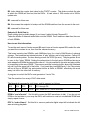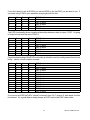
1
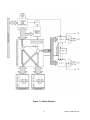
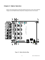
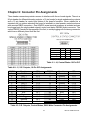
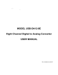
10623 Roselle Street, San Diego, CA 92121 C (858) 550-9559 C Fax (858) 550-7322
[email protected] C www.accesio.com
MODEL USB-DA12-8A
Eight Channel Digital to Analog Converter
with ARB (Arbitrary Waveform Generator)
USER MANUAL
FILE: MUSB-DA12-8A.B1d
Notice
The information in this document is provided for reference only. ACCES does not assume any liability arising out of
the application or use of the information or products described herein. This document may contain or reference
information and products protected by copyrights or patents and does not convey any license under the patent rights
of ACCES, nor the rights of others.
IBM PC, PC/XT, and PC/AT are registered trademarks of the International Business Machines Corporation.
Printed in U SA . Copyright 2005, 2007 by AC CES I/O Products In c, 1 0623 Ro selle Street, S an Die go, CA 92121. All
rights reserved.
WARNING!!
ALWAYS CONNECT AND DISCONNECT YOUR FIELD CABLING WITH THE
COMPUTER POWER OFF. ALWAYS TURN COMPUTER POWER OFF
BEFORE INSTALLING A CARD. CONNECTING AND DISCONNECTING
CABLES, OR INSTALLING CARDS INTO A SYSTEM WITH THE COMPUTER
OR FIELD POWER ON MAY CAUSE DAMAGE TO THE I/O CARD AND WILL
VOID ALL WARRANTIES, IMPLIED OR EXPRESSED.
2
Manual USB-DA12-8A
Warranty
Prior to shipm ent, AC CE S eq uipm ent is thorou ghly insp ecte d an d tested to applicable specification s. H ow ever, sh ould
equipment failure occu r, ACCE S assu res its custom ers that prom pt s ervice and support will be available. A ll
equipment originally manufactured by ACCES which is found to be defective will be repa ired or replaced su bjec t to
the following considerations.
Terms and Conditions
If a unit is suspected of failure, contact ACCES' Customer Service department. Be prepared to give the unit model
num ber, serial num ber, a nd a des cription of the failure s ym ptom (s). W e m ay suggest som e simp le tests to confirm
the failure. W e will assign a Return Material Authorization (RMA) num ber which must appear on the outer label of the
return package. All units/components should be properly packed for handling and returned with freight prepaid to the
ACCES designated Service Center, and will be returned to the customer's/user's site freight prepaid and invoiced.
Coverage
First Three Years: Returned unit/part will be repaired and/or replaced at ACCES option with no charge for labor or
parts not excluded by warranty. W arranty com m enc es w ith equ ipm ent shipm ent.
Following Years: T hroughout your eq uipm ent's lifetim e, A CCES sta nds ready to provide on-site or in-plant service
at reasonable rates sim ilar to those of other m anufacturers in the industry.
Equipment Not Manufactured by ACCES
Equipment pro vided but not m anufactured by ACCES is warranted and will be repaired acco rding to the terms and
conditions of the re spective equipm ent m anufacturer's w arranty.
General
Under this W arranty, lia bility of ACCES is lim ited to replacing, repairing or issuing credit (at ACCES discretion) for
any products which are proved to be defective during the warranty period. In no case is ACCES liable for
consequential or special damage arriving from use or misuse of our product. The customer is responsible fo r all
charges caused by modifications or additions to ACCES equipment not approved in writing by ACCES or, if in ACCES
opinion the equipment has been subjected to abnorm al use. "Ab norm al use" for pu rposes of this warranty is defined
as any use to which the equipment is exposed other than that use specified or intended as evidenced by purchase
or sales representation. Other than the above, no other warranty, expressed or im plied, s hall apply to any and all such
equipment furnished or sold by ACCES.
3
Manual USB-DA12-8A
Table of Contents
Chapter 1: Introduction . . . . . . . . . . . . . . . . . . . . . . . . . . . . . . . . . . . . . . . . . . . . . . . . . . . . . 5
Features . . . . . . . . . . . . . . . . . . . . . . . . . . . . . . . . . . . . . . . . . . . . . . . . . . . . . . . . . . . . . . . . . . . .
Applications . . . . . . . . . . . . . . . . . . . . . . . . . . . . . . . . . . . . . . . . . . . . . . . . . . . . . . . . . . . . . . . . . .
Functional Description . . . . . . . . . . . . . . . . . . . . . . . . . . . . . . . . . . . . . . . . . . . . . . . . . . . . . . . . . .
Model Options . . . . . . . . . . . . . . . . . . . . . . . . . . . . . . . . . . . . . . . . . . . . . . . . . . . . . . . . . . . . . . . .
Special Order . . . . . . . . . . . . . . . . . . . . . . . . . . . . . . . . . . . . . . . . . . . . . . . . . . . . . . . . . . . . . . . .
Included with your shipment . . . . . . . . . . . . . . . . . . . . . . . . . . . . . . . . . . . . . . . . . . . . . . . . . . . . .
Optional Accessories . . . . . . . . . . . . . . . . . . . . . . . . . . . . . . . . . . . . . . . . . . . . . . . . . . . . . . . . . . .
Specifications . . . . . . . . . . . . . . . . . . . . . . . . . . . . . . . . . . . . . . . . . . . . . . . . . . . . . . . . . . . . . . . .
5
5
5
6
6
6
6
7
Chapter 2: Installation . . . . . . . . . . . . . . . . . . . . . . . . . . . . . . . . . . . . . . . . . . . . . . . . . . . . . . 9
Software CD Installation . . . . . . . . . . . . . . . . . . . . . . . . . . . . . . . . . . . . . . . . . . . . . . . . . . . . . . . . 9
Hardware Installation . . . . . . . . . . . . . . . . . . . . . . . . . . . . . . . . . . . . . . . . . . . . . . . . . . . . . . . . . . . 9
USB I/O Quick-Start Guide . . . . . . . . . . . . . . . . . . . . . . . . . . . . . . . . . . . . . . . . . . . . . . . . . . . . . . 9
Chapter 3: Option Selection . . . . . . . . . . . . . . . . . . . . . . . . . . . . . . . . . . . . . . . . . . . . . . . . 10
DC Power Jack . . . . . . . . . . . . . . . . . . . . . . . . . . . . . . . . . . . . . . . . . . . . . . . . . . . . . . . . . . . . . .
Output Voltage Range Jumpers . . . . . . . . . . . . . . . . . . . . . . . . . . . . . . . . . . . . . . . . . . . . . . . . .
Differential Outputs (J3) . . . . . . . . . . . . . . . . . . . . . . . . . . . . . . . . . . . . . . . . . . . . . . . . . . . . . . .
Control and Monitoring (J4) . . . . . . . . . . . . . . . . . . . . . . . . . . . . . . . . . . . . . . . . . . . . . . . . . . . . .
Single Ended Outputs (J1) . . . . . . . . . . . . . . . . . . . . . . . . . . . . . . . . . . . . . . . . . . . . . . . . . . . . .
USB Connector . . . . . . . . . . . . . . . . . . . . . . . . . . . . . . . . . . . . . . . . . . . . . . . . . . . . . . . . . . . . . .
LED Light . . . . . . . . . . . . . . . . . . . . . . . . . . . . . . . . . . . . . . . . . . . . . . . . . . . . . . . . . . . . . . . . . .
11
11
11
11
11
11
11
Chapter 4: USB Address Information . . . . . . . . . . . . . . . . . . . . . . . . . . . . . . . . . . . . . . . . . 12
Chapter 5: Programming . . . . . . . . . . . . . . . . . . . . . . . . . . . . . . . . . . . . . . . . . . . . . . . . . . . 13
Software Reference Manual . . . . . . . . . . . . . . . . . . . . . . . . . . . . . . . . . . . . . . . . . . . . . . . . . . . . 13
Vendor Requests . . . . . . . . . . . . . . . . . . . . . . . . . . . . . . . . . . . . . . . . . . . . . . . . . . . . . . . . . . . . 13
USB-DA12-8A Vendor Request document text . . . . . . . . . . . . . . . . . . . . . . . . . . . . . . . . . . . . . . 13
Chapter 6: Connector Pin Assignments . . . . . . . . . . . . . . . . . . . . . . . . . . . . . . . . . . . . . . . 18
J4 Signal descriptions (Control / Status) . . . . . . . . . . . . . . . . . . . . . . . . . . . . . . . . . . . . . . . . . . . 19
ILDA DB-25 Pinout and Signal Description Standard Excerpts . . . . . . . . . . . . . . . . . . . . . . . . . . 21
References: . . . . . . . . . . . . . . . . . . . . . . . . . . . . . . . . . . . . . . . . . . . . . . . . . . . . . . . . . . . . . . . . 22
List of Figures
Figure 1-1: Block Diagram . . . . . . . . . . . . . . . . . . . . . . . . . . . . . . . . . . . . . . . . . . . . . . . . . . . . . . . . . . . . . . . . . . . . 8
Figure 3-1: Option Selection Map . . . . . . . . . . . . . . . . . . . . . . . . . . . . . . . . . . . . . . . . . . . . . . . . . . . . . . . . . . . . . . 10
List of Tables
Table
Ta ble
Ta ble
Ta ble
Ta ble
Table
6-1: J4, Control/Status 10-Pin IDC . . . . . . . . . . . . . . . . . . . . . . . . . . . . . . . . . . . . .
6-2: J1, S.E. O utpu ts, 16-Pin ID C A ssignm ents . . . . . . . . . . . . . . . . . . . . . . . . . . .
6-3: S.E . Ou tputs, Control/Status, DB 25 M ale C onn ecto r Pin A ssignm ents . . . . .
6-4: J3, Differential Analog O utpu ts, 26-Pin ID C A ssignm ents . . . . . . . . . . . . . . .
6-5: Differential Analog Ou tputs, DB 25F Conne ctor P in Assignm ents . . . . . . . . .
6-6: ILDA Signal Nam ing Standard, DB25F Signal Descriptions . . . . . . . . . . . . . .
4
.
.
.
.
.
.
.
.
.
.
.
.
..
..
..
..
..
..
.
.
.
.
.
.
.
.
.
.
.
.
......
......
......
......
......
......
.
.
.
.
.
.
.
.
.
.
.
.
..
..
..
..
..
..
.
.
.
.
.
.
.
.
.
.
.
.
Manual USB-DA12-8A
.
.
.
.
.
.
18
18
18
20
20
21
Chapter 1: Introduction
Features
•
•
•
•
•
•
•
•
•
•
•
•
•
•
High-speed USB 2.0 device, USB 1.1 compatible
Small, portable 8-channel, 12-bit, digital to analog converter outputs
Double-buffered allowing simultaneous update of all DAC’s
Up to 125K conversions per DAC per second
Streaming USB waveform data at over 400,000 DAC outputs per second total
ILDA (International Laser Display Association) compatible outputs
256K byte buffer on-board, or infinitely long streaming waveforms
Buffered waveforms at up to 1 million DAC conversions per second total
Analog output ranges of 0-2.5V, 0-5V, 0-10V, ±2.5V, ±5V, ±10V
Single-ended and differential outputs on separate connectors
Custom high-speed function driver
PC/104 module size and mounting compatibility
Small (4"x4"x1.75") rugged industrial enclosure
DB25M and DB25F enclosure mounted I/O connectors
Applications
•
•
•
•
•
Portable / Laptop
Education / Laboratory
Industrial Automation
Embedded OEM
ILDA Laser Driver
Functional Description
The USB-DA12-8A is an ideal solution for adding portable, easy-to-install analog outputs to any
computer with a USB port. The unit is a high speed USB 2.0 device, offering the highest speed
available with the USB bus. It is fully compatible with both USB 1.1 and USB 2.0 ports. The board
is plug-and-play allowing quick connection whenever you need additional I/O on a USB port.
This product features 8 digital-to-analog converters (DACs) with both differential and single-ended
outputs on separate connectors. The board features unipolar and bipolar ranges for each DAC
giving the user a variety of options. The DACs can be updated individually or simultaneously. To
ensure that there will not be excessive outputs to external circuits when the board is plugged in,
automatic circuits limit analog outputs to zero volts. Five Volt (5V) Power is supplied to the board
by an external regulated power supply which powers DC/DC converters to provide ±12V to the
operational amplifiers on the board. The I/O wiring depends on the model option(s) ordered. For
the OEM version, connections are via industry standard, IDC type 26-pin, 16-pin and 10-pin
connectors. For full, standard versions, connections are made to the IDC connectors on-board
via internal cables from enclosure mounted DB25 connectors, with one screw terminal accessory
being included (model ADAP25).
5
Manual USB-DA12-8A
The USB-DA12-8A is designed to be used in rugged industrial environments but is small enough
to fit nicely onto any desk or testing station. The board is PC/104 sized (3.550 by 3.775 inches)
and ships inside a steel powder-coated enclosure with an anti-skid bottom.
Model Options
USB-DA12-8A
-OEM
-PR
Module installed in an enclosure with two (2) DB25 I/O connectors
and one (1) screw terminal accessory (ADAP25)
Board only version with I/O headers
Power Adaptor, AC/DC 5V regulated.
Special Order
Resistors in series with differential connector for impedance matching, contact factory with your
requirement.
Included with your shipment
The following components are included with your shipment, depending on options ordered.
Please take the time now to ensure that no items are damaged or missing.
!
!
!
!
!
!
USB-DA12-8A
ADAP25, Screw Terminal Adaptor, qty 1
6' USB cable
115VAC to 5VDC Regulated Power Supply wall adaptor
Software Master CD
USB I/O Quick-Start Guide
Optional Accessories
!
!
ADAP25(M), Screw Terminal Adaptor (an additional unit could be needed if you
intended on using the Single-Ended and the Differential Analog Outputs).
-DIN DIN Rail Mounting Provision
6
Manual USB-DA12-8A
Specifications
Analog Outputs
Number of Outputs:
Type of Outputs:
Resolution:
Unipolar Ranges:
Bipolar Ranges:
Conversion Rate:
Relative Accuracy:
Differential Non-linearity:
Settling Time:
Output Current:
8 channels
Single-ended and differential
12-bit resolution
0-2.5V, 0-5V, 0-10V
±2.5V, ±5V, ±10V
125kHz, all channels simultaneous
±2 LSB typical
±0.2 LSB typical
8us typical, 10us max
6mA per channel
Bus Type
USB2.0 High-speed, USB1.1 Full-speed compatible
Environmental
Operating Temperature:
Storage Temperature:
Humidity:
Board Dimension:
Box Dimension:
0O to 70OC
-40O to +85OC
5% to 95% non-condensing
3.550 x 3.775 inches
4 x 4 x 1.75 inches tall
Power
+5VDC @ ~520mA typical, no-load on DAC outputs**
** Regulated AC/DC adapter should be ordered (“-PR” option) together with the board as
the minimum current draw exceeds that which the USB port can provide by default.
7
Manual USB-DA12-8A
Figure 1-1: Block Diagram
8
Manual USB-DA12-8A
Chapter 2: Installation
Software CD Installation
This paragraph is intended to detail the software installation steps.
The software provided with this board is contained on one CD and must be installed
onto your hard disk prior to use. To do this, perform the following steps as appropriate
for your software format and operating system. Substitute the appropriate drive letter for
your CD-ROM or disk drive where you see d: in the examples below.
WIN95/98/Me/NT/2000/XP/2003
a.
b.
c.
Place the CD into your CD-ROM drive.
The CD should automatically run the install program. If the install program does
not click START | RUN and type d:install, click OK or press K.
Follow the on-screen prompts to install the software for this board.
Hardware Installation
The USB-DA12-8A board can be installed in any USB 2.0 or USB 1.1 port. Please refer
to the USB I/O Quick Start Guide which can be found on the CD, for specific, quick
steps to complete the hardware and software installation.
USB I/O Quick-Start Guide
Provides quick and straight-forward steps to complete the software and hardware
installation of this product in your system.
9
Manual USB-DA12-8A
Chapter 3: Option Selection
Refer to the setup programs on the CD provided with the board. Also, refer to the Block
Diagram and the Option Selection Map when reading this section of the manual.
Figure 3-1: Option Selection Map
10
Manual USB-DA12-8A
DC Power Jack
This is the DC input connector used to provide a regulated +5V power supply to the card
without using the USB bus. Be sure to order option -PR so this wall adaptor will be included
with your shipment.
Output Voltage Range Jumpers
Use the jumpers to select the range that you wish to use. Each channel is configured
individually for the following output possibilities.
0 to 2.5V
0 to 5V
0 to 10V
-2.5 to 2.5V
-5 to 5V
-10 to 10 V
Differential Outputs (J3)
These are the Differential DAC outputs.
Control and Monitoring (J4)
This 10-pin connector provides an alternate means to start and stop the ARB and monitor it’s
status.
Single Ended Outputs (J1)
These are the Single Ended DAC outputs.
USB Connector
The USB connector on this board is a USB type B.
LED Light
LED indicates Power and Activity
11
Manual USB-DA12-8A
Chapter 4: USB Address Information
Use the provided driver to access the USB board. This driver will allow you to determine how
many supported USB devices are currently installed, and each device’s type. This information
is returned as a Vendor ID (VID), Product ID (PID) and Device Index.
The board’s VID is “0x1605", and its PID is “0x8001".
The Device Index is determined by how many of the device you have in your system, and
provides a unique identifier allowing you to access a specific board at will.
12
Manual USB-DA12-8A
Chapter 5: Programming
The installation program on the CD will install four PDF manuals to your hard drive. These are
the USB I/O Quick-Start Guide, User Manual, Software Reference Manual, and super-softwaretech manual; Vendor Requests.
Software Reference Manual
Details our various drivers and sample programs in a number of programming languages
as well as providing insight into the most optimum combination of language,
environment/OS and hardware selection available.
Vendor Requests
This file provides information on a RAW USB INTERFACE for very low-level
programming, generally in Operating Systems other than Windows.
USB-DA12-8A Vendor Request document text
This device was originally designed for ILDA waveform playback. ILDA is used heavily in the
laser “movie” environment, for laser light-shows. As a result, much of the terminology used in
this document refers to a “movie” file. In every case where “movie” occurs you can use
“waveform” just as precisely. Where you see movie-centric terms like “play” you can substitute
“start” or “run”.
Vendor Specific (endpoint 0, control) Requests B0, B1, B2, B3, B4, and B5 (hex) are defined
by the firmware.
(Just to define some terms:
setupdat[5] is MSB of "index", setupdat[4] is LSB of index.
setupdat[3] is MSB of "value", setupdat[2] is LSB of value.
)
Endpoint 0 Vendor Requests:
B0: One byte passed down in Value (setupdat[2]). Bit 7 is "reset", d6 is "pause", d0 is "play"
If D7 is set, the cpld is reset, run is stopped, and the LEDs are reset to off.
If D6 is set nothing particular happens. This bit is reserved for future use.
If D0 is set the DAC reference voltage is woken up (voltage starts coming out the DACs), and
the SRAM starts playing.
B1: setupdat[4] is LSB and setupdat[5] is MSB, of the location in the onboard SRAM that bulk
transfers should load into. Each bank is 0x1FFF in size. Bank 0 through Bank 7 map
contiguously to create a 0xFFFF byte buffer. Writing to the 0xFFFFth byte causes the SRAM
to toggle to the other SRAM. Setupdat[3] is the "bank", and only 0-7 are valid. B1 must be
called before endpoint 2 can be used to load the data into the SRAM.
13
Manual USB-DA12-8A
B2: Index holds the counter load value for the "RATE" counter. This divisor controls the rate
at which the SRAM will feed out into the DACs. A load value of 190h works out to 30KHz
update rate.
B3: reserved for future use
B4: this causes the endpoint to lockup until the SRAM switches from the current to the next.
B5: reserved for future use
Endpoint 2: Bulk Data In
Does nothing (and probably hangs) if you haven't called Vendor Request B1
Takes the blocks of data and writes them into the SRAM. Don't load more data than the sum
of both SRAMs.
How to use this information:
To use the card, issue a Vendor request B0-reset, issue a Vendor request B2 to select the rate
you want the counters to run, then load the onboard memory.
This board contains two SRAMs, each 64KBytes long, for a total of 64KWords of onboard
storage. The board has two internal pointers, a “play” pointer, and a “write’ pointer. Calling VR
B1 sets the write pointer. So does issuing a reset via VR B0 (to zero). The play pointer is set
to zero, in the *other* SRAM. Setting the write pointer to the last spot in SRAM and issuing a
write swaps the SRAMs the two pointers refer to. It is not possible for the write and play pointer
to be pointing to the same SRAM. This memory acts like a circular buffer, where the head and
tail can’t be in the same half of the buffer. If you reset then load 64KWords-1, the Play pointer
will be at Zero in SRAM0, the write pointer will be at 0xfffe in SRAM1, effectively one word
away, but still in the other half of memory.
A program to control the DACs must generate a "movie" file.
This file consists of an array of DAC data words.
The format of one word is both binary and bit-mapped as follows:
D15
D14
D13
D12
D11 through D0
EOM
EOF
EOD
LOOP
DAC Value 0-FFF, hex 0-4095 dec
EOM is “end of movie”. Set this bit to cause the DAC waveforms to halt. If you do not set
EOM on the last data in your array the DACs will continue to read out uninitialized SRAM and
simply repeat forever.
EOF is “end-of-frame”. Set this bit to cause a particular digital output bit to indicate the bit
was set during playback.
14
Manual USB-DA12-8A
EOD is “end-of-DACs”. Set this bit to indicate “start counting DACs over at zero” (see below)
LOOP is “loop”, and can be set to cause the circuit to set the internal pointer into the current
location in SRAM back to “zero” in the first SRAM. If you load a small array of DAC data and
set loop on the last data point, it will simply play forever (unless EOM was set somewhere
before loop)
The format of the array:
The array contains data for all DACs interleaved. The simplest possible array would look like
this:
0
0
0
0
DAC 0 value
0
0
0
0
DAC 1 value
0
0
0
0
DAC 2 value
0
0
0
0
DAC 3 value
0
0
0
0
DAC 4 value
0
0
0
0
DAC 5 value
0
0
0
0
DAC 6 value
1
0
0
0
DAC 7 value
Running this movie would cause the card to initialize the 8 dac values then stop, effectively
creating a DC output on all DACs. (Note, you could have cleared EOM and set LOOP for the
same effect, but you would then waste cycles repeating the same DC data)
If you wanted to produce a square wave on all DACs you could double the waveform buffer and
loop:
0
0
0
0
0
0
0
0
0
0
0
0
0
0
0
0
0
0
0
0
0
0
0
0
0
0
0
0
0
0
0
0
0
0
0
0
0
0
0
0
0
0
0
0
0
0
0
0
0
0
0
0
0
0
0
0
0
0
0
0
0
0
0
1
DAC 0 value
DAC 1 value
DAC 2 value
DAC 3 value
DAC 4 value
DAC 5 value
DAC 6 value
DAC 7 value
DAC 0 value
DAC 1 value
DAC 2 value
DAC 3 value
DAC 4 value
DAC 5 value
DAC 6 value
DAC 7 value
15
Manual USB-DA12-8A
If you don’t want to use all 8 DACs you can set EOD on the last DAC you do want to use. If
you were using 3 DACs your waveform array might look like this:
0
0
0
0
0
0
0
0
0
0
0
0
0
0
1
0
0
1
0
0
0
0
0
1
DAC 0 value
DAC 1 value
DAC 2 value
DAC 0 value
DAC 1 value
DAC 2 value
This EOD functionality allows complex relationships between rates of output. If DAC 1 is going
to output at one-third the rate of DAC 0:
0
0
0
0
0
0
0
0
0
0
0
0
0
0
0
0
1
1
0
1
1
1
0
1
0
0
0
0
0
0
0
1
DAC 0 value
DAC 0 value
DAC 0 value
DAC 1 value
DAC 0 value
DAC 0 value
DAC 0 value
DAC 1 value
Careful understanding of this EOD functionality is critical to correctly creating a waveform/movie
buffer. Here’s a more complex example.
0
0
0
0
0
0
0
0
0
0
0
0
0
0
0
0
0
0
0
0
0
0
0
0
0
0
0
0
1
0
0
1
1
0
0
0
0
0
1
0
1
0
0
0
0
0
0
0
0
0
0
0
0
0
0
1
DAC 0 value
DAC 0 value
DAC 1 value
DAC 2 value
DAC 0 value
DAC 0 value
DAC 1 value
DAC 2 value
DAC 3 value
DAC 4 value
DAC 5 value
DAC 0 value
DAC 1 value
DAC 0 value
If you never set EOD the DACs *should* increment from 0 to 7, wrap to 0, and repeat, but this
is untested. It’s a good idea to simply always set EOD on the last DAC’s data value.
16
Manual USB-DA12-8A
Loading the array:
The array is loaded by issuing a vendor request (VR) B1 to specify the starting location of the
next buffer in the SRAM. Typically VR B1 with “0000" and “bank 0" in the parameters (refer to
the discussion of VR B1, above) is the first instruction issued.
Then, EP2 bulk transfers are initiated for the first 64KWords of your waveform file. If your
waveform is smaller than 64KWords, simply load the entire waveform (and you’ll want EOM or
LOOP set to avoid playing uninitialized SRAM.)
If your waveform is smaller than 32KWords you must take an extra step: Issue a VR B1
with 1FFE/Bank7, then EP2 a single WORD. This sets the internal “write” pointer into
the second SRAM. This is necessary because the “Play” pointer is always in the SRAM
you’re NOT writing into.
If your waveform is smaller than 64KWords there is no streaming needed, simply issue a VR
B0 “run” command to cause the DACs to start outputting data.
If your waveform is larger than the onboard memory, load more than one 32KWords but less
than 64KWords with your file, then issue a “run”, then continue loading your file.
The EP2 Bulk transfers to load the SRAM will *hang* until there is room in the SRAM for more
data. Your code must handle this apparent lockup. Multithreaded is recommended.
17
Manual USB-DA12-8A
Chapter 6: Connector Pin Assignments
Three header connectors provide a means to interface with the on-board signals. There is a
26 pin header for differential analog outputs, a 16 pin header for single ended analog outputs
and a 10 pin header for control and status of the board’s functions. When ordered as a
standard unit (no options selected) the board is installed in a steel powder coated enclosure
with mounted DB25 connectors. One ADAP25 screw terminal accessory is included and can
be plugged onto the single ended outputs/ control and status DB25M (male) connector. The
second DB25F (female) is the opposite of the first, to avoid plugging onto the wrong connector
which has a different pinout than the first.
Function
Pin
Pin
EOF
1
2
Function
EOD
Status
3
4
Blank
Ext. Trigger
5
6
Pause
Interlock
7
8
Loop
Ground
9
10
N/C
Table 6-1: J4, Control/Status 10-Pin IDC
Table 6-2: J1, S.E. Outputs, 16-Pin IDC Assignments
DB25M
1
2
3
4
5
6
7
8
9
10
11
12
13
Function
DAC 0
DAC 1
DAC 2
DAC 3
DAC 4
DAC 5
DAC 6
DAC 7
EOF
Status
Ext. Trigger
Interlock
Ground
IDC
J1-1
J1-3
J1-5
J1-7
J1-9
J1-11
J1-13
J1-15
J4-1
J4-3
J4-5
J4-7
J4-9
DB25M
14
15
16
17
18
19
20
21
22
23
24
25
Function
Ground
Ground
Ground
Ground
Ground
Ground
Ground
Ground
EOD
Blank
Pause
Loop
IDC
J1-2
J1-4
J1-6
J1-8
J1-10
J1-12
J1-14
J1-16
J4-2
J4-4
J4-6
J4-8
Table 6-3: S.E. Outputs, Control/Status, DB25 Male Connector Pin Assignments
18
Manual USB-DA12-8A
J4 Signal descriptions (Control / Status)
Outputs:
EOF
EOD
STATUS
BLANK
“End of Frame”, output every time EOF is issued.
“End of DAC”, output every time DAC starts at 0.
User controlled via Firmware.
Output blanking signal from top bits of EOM, EOF, EOD....
Inputs:
EXT. TRIGGER
PAUSE
INTERLOCK
LOOP
To Ctr 0, starts D/A conversions.
To gate 0 of counter.
“Shutdown” Digital Input (Firmware controlled).
Loops contents of SRAM, resets pointer to beginning of
SRAM 0.
All signals at J4 pass through a line buffer, and all input signals are pulled to +5V through
47Kohms each. Activate input signals by applying 0V or a ground to the associated pin.
19
Manual USB-DA12-8A
Table 6-4: J3, Differential Analog Outputs, 26-Pin IDC Assignments
DB25F
Function
IDC
IDC
Function
DB25F
1
DAC 0+
1
2
DAC 0-
14
2
DAC 1+
3
4
DAC 1-
15
3
DAC 2+
5
6
DAC 2-
16
4
Interlock
7
8
Interlock
17
5
DAC 3+
9
10
DAC 3-
18
6
DAC 4+
11
12
DAC 4-
19
7
DAC 5+
13
14
DAC 5-
20
8
DAC 6+
15
16
DAC 6-
21
9
DAC 7+
17
18
DAC 7-
22
10
N/C
19
20
N/C
23
11
N/C
21
22
N/C
24
12
N/C
23
24
N/C
25
13
Ground
25
26
N/C
N/C
Table 6-5: Differential Analog Outputs, DB25F Connector Pin Assignments
20
Manual USB-DA12-8A
ILDA DB-25 Pinout and Signal Description Standard Excerpts
Pins
Signal Names Signal Description
1, 14 X+, X-
Controls the horizontal beam position. This is a bipolar analog signal whose voltage range is 10V peak-to-peak differential.
A differential voltage level of -10V shall deflect the laser beam to the left side of the projection area. A differential voltage
level of +10V shall deflect the signal to the right side. A differential voltage of +10V occurs if the normal signal line has a
voltage level of +10V with respect to the voltage level of the inverted signal line. When compared to the ground level of the
differential driver, the voltage level of the normal signal line shall be +5V and the level of the inverted signal shall be -5V.
2, 15 Y+, Y-
Controls the vertical beam position. This is a bipolar analog signal whose voltage range is 10V peak-to-peak differential. A
differential voltage level of -10V shall deflect the laser beam to the bottom of the screen. A differential voltage level of
+10V shall deflect the signal to the top of the screen. A differential voltage level of 0V shall place the beam in the center of
the screen vertically. A differential voltage of +10V occurs if the normal signal line has a voltage level of +10V with respect
to the voltage level of the inverted signal line. When compared to the ground level of the differential driver, the voltage level
of the normal signal line shall be +5V and the voltage level of the inverted signal shall be -5V.
3, 16 Intensity +
Intensity 4, 17 Interlock A
Interlock B
These are intended to keep the projector from outputting light if inadvertently connected to nonlaser signal sources such as
SCSI, Parallel or serial connectors. These signals are also a fail-safe should other control measures fail. These signals are
tied together at the signal source. If this loop is broken, it is required that projectors close a shutter or turn off the laser or
take other actions that prevent light from being emitted from the projector. It is important to note that this portion of the
ISPDB25 is a projector interlock which may be separate from the remote interlock connector on a laser used with the
projector.
5, 18 R+, R-
Controls the red intensity. This is a unipolar analog signal whose voltage range is 5V peak-to-peak differential. A
differential voltage level of 0V shall produce no red output. A differential voltage level of +5V shall produce maximum red
output. A differential voltage of +5V occurs if the normal signal line has a voltage level of +5V with respect to the voltage
level of the inverted signal line. When compared to the ground level of the differential driver, the voltage level of the normal
signal line shall be +2.5V and the voltage level of the inverted signal shall be -2.5V.
6, 19 G+, G-
Controls the green intensity. This is a unipolar analog signal whose voltage range is 5V peak-to-peak differential. A
differential voltage level of 0V shall produce no green output. A differential voltage level of +5V shall produce maximum
green output. A differential voltage of +5V occurs if the normal signal line has a voltage level of +5V with respect to the
voltage level of the inverted signal line. When compared to the ground level of the differential driver, the voltage level of the
normal signal line shall be +2.5V and the voltage level of the inverted signal shall be -2.5V.
7, 20 B+, B-
Controls the blue intensity. This is a unipolar analog signal whose voltage range is 5V peak-to-peak differential. A
differential voltage level of 0V shall produce no blue output. A differential voltage level of +5V shall produce maximum
blue output. A differential voltage of +5V occurs if the normal signal line has a voltage level of +5V with respect to the
voltage level of the inverted signal line. When compared to the ground level of the differential driver, the voltage level of the
normal signal line shall be +2.5V and the voltage level of the inverted signal shall be -2.5V.
8, 21 User-defined signal 1+, 19, 22 User-defined signal 2+, 210,23 User-defined signal 3+, 311,24 User-defined signal 4+, 412
Projector
Return signal
13
Shutter
Optical shutter intended to extinguish all light from the graphics scanners. This is a unipolar analog signal whose voltage
range is 5 volts peak. The shutter signal is referenced to the Ground pin. A voltage level of 0 volts shall close the shutter so
that no light is emitted from the graphics scanners. A voltage level of +5 volts shall fully open the shutter.
25
Ground
0 voltage potential reference and signal shield.
Table 6-6: ILDA Signal Naming Standard, DB25F Signal Descriptions
This material is copyright © 1999 by the International Laser Display Association and is used by permission.
21
Manual USB-DA12-8A
References:
International Laser Display Association
http://www.laserist.org/index.htm
Customer Comments
If you experience any problems with this manual or just want to give us some feedback, please
email us at: [email protected]. Please detail any errors you find and include your mailing
address so that we can send you any manual updates.
10623 Roselle Street, San Diego CA 92121
Tel. (858)550-9559 FAX (858)550-7322
www.accesio.com
22
Manual USB-DA12-8A