1
TM
TNT4882
Programmer Reference Manual
July 1995 Edition
Part Number 370872A-01
© Copyright 1993, 1995 National Instruments Corporation.
All Rights Reserved.
National Instruments Corporate Headquarters
6504 Bridge Point Parkway
Austin, TX 78730-5039
(512) 794-0100
Technical support fax: (800) 328-2203
(512) 794-5678
Branch Offices:
Australia 03 9 879 9422, Austria 0662 45 79 90 0, Belgium 02 757 00 20,
Canada (Ontario) 519 622 9310, Canada (Québec) 514 694 8521,
Denmark 45 76 26 00, Finland 90 527 2321, France 1 48 14 24 24,
Germany 089 741 31 30, Hong Kong 2645 3186, Italy 02 48301892,
Japan 03 5472 2970, Korea 02 596 7456, Mexico 5 202 2544,
Netherlands 03480 33466, Norway 32 84 84 00, Singapore 2265886,
Spain 91 640 0085, Sweden 08 730 49 70, Switzerland 056 20 51 51,
Taiwan 02 377 1200, U.K. 01635 523545
Limited Warranty
The TNT4882™ integrated circuit (“equipment”) is warranted against defects in material
and workmanship under normal use and service for a period of one (1) year from the date
of shipment from the National Instruments factory. During this period of one year,
National Instruments shall at its sole option either repair, replace, or credit the Buyer for
defective equipment if: (i) Buyer returns the equipment to National Instruments, FOB the
National Instruments factory in Austin, Texas; (ii) Buyer notifies National Instruments
promptly upon discovery of any defect in writing, including a detailed description of the
defect; and (iii) upon examination of the returned equipment, National Instruments is
satisfied that the circuit is defective and that the cause of such defect is not alteration or
repair by someone other than National Instruments, neglect, accident, misuse, improper
installation, or use contrary to any instructions issued by National Instruments.
A Return Material Authorization (RMA) number must be obtained from the factory and
clearly marked on the outside of the package before any equipment will be accepted for
warranty work. Prior to issuance of an RMA by National Instruments, Buyer shall allow
National Instruments the opportunity to inspect the equipment on-site at Buyer’s facility.
This warranty expires one year from date of original shipment regardless of any warranty
performance during that warranty period. The warranty provided herein is Buyer’s sole
and exclusive remedy for nonconformity of the equipment or for breach of any warranty.
THE ABOVE IS IN LIEU OF ALL OTHER WARRANTIES EXPRESSED OR
IMPLIED. NATIONAL INSTRUMENTS SPECIFICALLY DISCLAIMS THE
IMPLIED WARRANTIES OF MERCHANTIBILITY AND FITNESS FOR A
PARTICULAR PURPOSE. BUYER’S RIGHT TO RECOVER DAMAGES CAUSED
BY FAULT OR NEGLIGENCE ON THE PART OF NATIONAL INSTRUMENTS
SHALL BE LIMITED TO THE AMOUNT THERETOFORE PAID BY THE BUYER.
NATIONAL INSTRUMENTS WILL NOT BE LIABLE FOR DAMAGES RESULTING
FROM LOSS OF DATA, PROFITS, USE OF PRODUCTS, OR INCIDENTAL OR
CONSEQUENTIAL DAMAGES, EVEN IF ADVISED OF THE POSSIBILITY
THEREOF. This limitation of the liability of National Instruments will apply regardless
of the form of action, whether in contract or tort, including negligence. National
Instruments recommends against the use of its products as critical components in any life
support devices or systems whose failure to perform can reasonably be expected to cause
significant injury to a human. Buyer assumes all risk for such application and agrees to
indemnify National Instruments for all damages which may be incurred due to use of the
National Instruments standard devices in medical or life support applications. Any action
against National Instruments must be brought within one year after the cause of action
accrues.
National Instruments believes that the information in this manual is accurate. The
document has been carefully reviewed for technical accuracy. In the event that technical
or typographical errors exist, National Instruments reserves the right to make changes to
subsequent editions of this document without prior notice to holders of this edition. The
reader should consult National Instruments if errors are suspected. In no event shall
National Instruments be liable for any damages arising out of or related to this document
or the information contained in it.
Copyright
nder the copyright laws, this publication may not be reproduced or transmitted in any
form, electronic or mechanical, including photocopying, recording, storing in an
information retrieval system, or translating, in whole or in part, without the prior written
consent of National Instruments Corporation.
Trademarks
NAT4882 ®, Turbo488®, and TNT4882™, are trademarks of National Instruments
Corporation.
Product and company names listed are trademarks or trade names of their respective
companies.
WARNING REGARDING MEDICAL AND CLINICAL
USE OF NATIONAL INSTRUMENTS PRODUCTS
National Instruments products are not designed with components and testing intended to
ensure a level of reliability suitable for use in treatment and diagnosis of humans.
Applications of National Instruments products involving medical or clinical treatment can
create a potential for accidental injury caused by product failure, or by errors on the part
of the user or application designer. Any use or application of National Instruments
products for or involving medical or clinical treatment must be performed by properly
trained and qualified medical personnel, and all traditional medical safeguards,
equipment, and procedures that are appropriate in the particular situation to prevent
serious injury or death should always continue to be used when National Instruments
products are being used. National Instruments products are NOT intended to be a
substitute for any form of established process, procedure, or equipment used to monitor
or safeguard human health and safety in medical or clinical treatment.
Contents
About This Manual ............................................................................................. xvii
Organization of This Manual ......................................................................... xvii
Conventions Used in This Manual................................................................. xviii
Related Documentation ................................................................................. xviii
Customer Communication ............................................................................. xix
Chapter 1
Introduction and General Description ........................................................ 1-1
TNT4882 Features ......................................................................................... 1-1
IEEE 488 Capabilities ..................................................................... 1-1
CPU Interface Features ................................................................... 1-4
Bus Interface Capabilities ............................................................... 1-4
Chapter 2
TNT4882 Architectures ..................................................................................... 2-1
Turbo+7210 Mode ......................................................................................... 2-1
Turbo+9914 Mode ......................................................................................... 2-2
One-Chip Mode ............................................................................................. 2-2
Choosing a TNT4882 Architecture Mode ..................................................... 2-2
One-Chip Mode ............................................................................... 2-2
Turbo+9914 Mode ........................................................................... 2-3
Turbo+7210 Mode ........................................................................... 2-3
Changing the TNT4882 Architecture Modes ................................................ 2-3
Architecture After a Hardware Reset .............................................. 2-4
Changing between Turbo+9914 Mode and
Turbo+7210 Mode ........................................................................... 2-4
Changing between One-Chip Mode and Turbo+7210 Mode .......... 2-4
Chapter 3
TNT4882 Interface Registers .......................................................................... 3-1
One-Chip Mode/Turbo+7210 Mode Registers .............................................. 3-1
Hidden Registers: One-Chip Mode/Turbo+7210 Mode ................. 3-4
Address Register Map ....................................................... 3-4
Auxiliary Mode Register Map .......................................... 3-4
SH_CNT Map ................................................................... 3-5
The Page-In State (One-Chip Mode/Turbo+7210 Mode) ............... 3-5
When to Use the Page-In State ......................................... 3-5
How to Page-In ................................................................. 3-6
Turbo+9914 Mode Registers ......................................................................... 3-7
Hidden Registers: Turbo+9914 Mode ............................................ 3-9
Accessory Read Register Map .......................................... 3-9
The SWAP Bit ................................................................................. 3-9
Setting the SWAP Bit ....................................................... 3-9
© National Instruments Corp.
v
TNT4882 Programmer Reference
Contents
Recommendation .............................................................. 3-10
The Page-In Condition (Turbo+9914 Mode) .................................. 3-10
Register Bit Descriptions ............................................................................... 3-10
8-Bit Versus 16-Bit Accesses.......................................................... 3-10
9914 and 7210 Registers with Identical Names .............................. 3-11
Accessory Register A (ACCRA) ..................................................... 3-12
Accessory Register B (ACCRB) ..................................................... 3-13
Accessory Register E (ACCRE) ..................................................... 3-14
Accessory Register F (ACCRF) ...................................................... 3-15
Accessory Register I (ACCRI)........................................................ 3-16
Accessory Register J (ACCRJ) ....................................................... 3-17
Accessory Write Register (ACCWR) ............................................. 3-19
Address Mode Register (ADMR) ................................................... 3-20
Address Register (ADR)—One-Chip Mode,
Turbo+7210 Mode ........................................................................... 3-22
Address Register (ADR)—Turbo+9914 Mode ............................... 3-23
Address Register 0 (ADR0)............................................................. 3-24
Address Register 1 (ADR1)............................................................. 3-25
Address Status Register (ADSR)—Turbo+7210 Mode .................. 3-26
Address Status Register (ADSR)—Turbo+9914 Mode .................. 3-29
Auxiliary Command Register (AUXCR) ........................................ 3-32
Auxiliary Mode Register (AUXMR)............................................... 3-41
Auxiliary Register A (AUXRA) ..................................................... 3-51
Auxiliary Register B (AUXRB) ...................................................... 3-53
Auxiliary Register E (AUXRE)....................................................... 3-55
Auxiliary Register F (AUXRF) ....................................................... 3-56
Auxiliary Register G (AUXRG) ..................................................... 3-57
Auxiliary Register I (AUXRI) ......................................................... 3-59
Auxiliary Register J (AUXRJ) ........................................................ 3-61
Bus Control Register (BCR)/Bus Status Register (BSR) ................ 3-63
Carry Cycle Register (CCR) ........................................................... 3-64
Command/Data Out Register (CDOR) ........................................... 3-65
Configuration Register (CFG) ......................................................... 3-66
Command Register (CMDR)........................................................... 3-69
Count 0 Register (CNT0) ................................................................ 3-71
Count 1 Register (CNT1) ................................................................ 3-71
Count 2 Register (CNT2) ................................................................ 3-71
Count 3 Register (CNT3) ................................................................ 3-71
Count Registers ............................................................................... 3-72
32-Bit Mode ...................................................................... 3-72
16-Bit Mode ...................................................................... 3-72
Command Pass Through Register (CPTR) ..................................... 3-73
Chip Signature Register (CSR) ....................................................... 3-74
DIO Control Register (DCR)........................................................... 3-75
Data In Register (DIR) .................................................................... 3-76
DIO Status Register (DSR) ............................................................. 3-77
End-of-String Register (EOSR)....................................................... 3-78
First-In First-Out Buffer (FIFO(A/B)) ............................................ 3-79
TNT4882 Programmer Reference
vi
© National Instruments Corp.
Contents
FIFO A .............................................................................. 3-79
FIFO B .............................................................................. 3-79
High-Speed Enable Register (HIER)............................................... 3-81
Handshake Select Register (HSSEL) .............................................. 3-83
Interrupt Mask Register 0 (IMR0)—One-Chip Mode,
Turbo+7210 Mode ........................................................................... 3-84
Interrupt Status Register 0 (ISR0)—One-Chip Mode,
Turbo+7210 Mode ........................................................................... 3-84
Interrupt Mask Register 0 (IMR0)—Turbo+9914 Mode ................ 3-88
Interrupt Status Register 0 (ISR0)—Turbo+9914 Mode ................. 3-88
Interrupt Mask Register 1 (IMR1)—One-Chip Mode,
Turbo+7210 Mode ........................................................................... 3-92
Interrupt Status Register 1 (ISR1)—One-Chip Mode,
Turbo+7210 Mode ........................................................................... 3-92
Interrupt Mask Register 1 (IMR1)—Turbo+9914 Mode ................ 3-98
Interrupt Status Register 1 (ISR1)—Turbo+9914 Mode ................. 3-98
Interrupt Mask Register 2 (IMR2)—One-Chip Mode,
Turbo+7210 Mode ........................................................................... 3-103
Interrupt Status Register 2 (ISR2)—One-Chip Mode,
Turbo+7210 Mode ........................................................................... 3-103
Interrupt Mask Register 2 (IMR2)—Turbo+9914 Mode ................ 3-107
Interrupt Status Register 2 (ISR2)—Turbo+9914 Mode ................. 3-107
Interrupt Mask Register 3 (IMR3)................................................... 3-111
Interrupt Status Register 3 (ISR3) ................................................... 3-111
Board Interrupt Register (INTR) ..................................................... 3-114
Key Control Register (KEYREG) ................................................... 3-115
Miscellaneous Register (MISC) ...................................................... 3-117
Parallel Poll Register (PPR)—Turbo+7210 Mode .......................... 3-119
Parallel Poll Register (PPR)—Turbo+9914 Mode .......................... 3-122
Programmable T1 Register (PT1) .................................................. 3-123
Source/Acceptor Status Register (SASR) ....................................... 3-124
SH_CNT Register (SH_CNT)........................................................ 3-126
Serial Poll Mode Register (SPMR) ................................................. 3-127
Serial Poll Status Register (SPSR) .................................................. 3-127
Status 1 Register (STS1) ................................................................. 3-129
Status 2 Register (STS2) ................................................................. 3-132
T12 Register (T12) ......................................................................... 3-133
T13 Register (T13) .......................................................................... 3-134
T17 Register (T17) .......................................................................... 3-135
Timer Register (TIMER) ................................................................. 3-136
Chapter 4
TNT4882 Programming Considerations .................................................... 4-1
Chip Initialization .......................................................................................... 4-1
1. Reset the Turbo488 Circuitry of the TNT4882 .......................... 4-1
2. Place the TNT4882 in Turbo+7210 Mode ................................. 4-1
3. Configure the TNT4882 for One-Chip Mode ............................ 4-2
4. Make Sure that the Local Power-On Message is Asserted ........ 4-2
© National Instruments Corp.
vii
TNT4882 Programmer Reference
Contents
5. Configure the TNT4882 for GPIB Operation ............................ 4-2
A. Set the GPIB Address(es) .......................................... 4-2
B. Write the Initial Serial Poll Response........................ 4-2
C. Configure the Initial Parallel Response ..................... 4-2
D. Enable Interrupts........................................................ 4-3
E. Set the GPIB Handshake Parameters ......................... 4-3
6. Clear the Local Power-On Message to Begin
GPIB Operation.......................................................................... 4-3
GPIB Talker or Listener Considerations ....................................................... 4-3
GPIB Addressing ............................................................................. 4-3
Logical and Physical Devices ........................................... 4-3
Normal and Extended Addressing .................................... 4-3
Implementing One Logical Device:
Normal Addressing ........................................................... 4-4
Implementing One Logical Device:
Extended Addressing ........................................................ 4-4
Implementing Two Logical Devices:
Normal Addressing ........................................................... 4-4
Implementing Two Logical Devices:
Extended Addressing ........................................................ 4-5
Implementing Three or More Logical Devices:
Normal Addressing ........................................................... 4-6
Implementing Three or More Logical Devices:
Extended Addressing ........................................................ 4-7
Programmed Implementation of a Talker and Listener................... 4-7
GPIB Data Transfers...................................................................................... 4-7
Initialization..................................................................................... 4-7
Conducting the Transfer .................................................................. 4-8
Programmed I/O................................................................ 4-9
Interrupt-Driven Status Reporting .................................... 4-11
DMA ................................................................................. 4-11
Termination ..................................................................................... 4-12
Terminal Count ................................................................. 4-12
TLCINT Signal ................................................................. 4-12
Software Abort .................................................................. 4-12
Post Termination ............................................................................. 4-12
Device Status Reporting ................................................................................ 4-13
Requesting Service .......................................................................... 4-13
Asserting the SRQ signal .................................................. 4-13
IEEE 488.2 Service Requesting ........................................ 4-13
7210-Style Service Requesting ......................................... 4-13
Responding to Serial Polls............................................................... 4-14
Responding to Parallel Polls ........................................................... 4-14
The ist Message ................................................................. 4-14
Remote Configuration ....................................................... 4-14
Local Configuration .......................................................... 4-15
Disabling the Parallel Poll Response ................................ 4-15
Acceptor Handshake Holdoffs in One-Chip Mode ....................................... 4-15
TNT4882 Programmer Reference
viii
© National Instruments Corp.
Contents
The GPIB rdy Message and RFD Holdoffs..................................... 4-15
Generating the rdy Message.............................................. 4-15
Immediate RFD Holdoff ................................................... 4-15
Data Byte RFD Holdoffs................................................... 4-16
DAC Holdoffs ................................................................................. 4-16
Determining When DAC Holdoffs Occur......................... 4-17
Hardware Interrupts ....................................................................................... 4-18
The INTR Pin .................................................................................. 4-18
The TNT4882_INT Signal .............................................................. 4-18
The TLCINT Signal ........................................................................ 4-18
Using the Timer ............................................................................................. 4-19
The Timer ........................................................................................ 4-19
Global Timeouts .............................................................................. 4-19
Byte Timeouts ................................................................................. 4-19
Remote/Local State Considerations ............................................................... 4-19
Device Triggering .......................................................................................... 4-20
Device Clearing ............................................................................................. 4-20
Using the KEY Pins ....................................................................................... 4-21
Writing a DS1204 Key .................................................................... 4-21
Reading a DS1204 Key ................................................................... 4-21
Using the Key Pins as General Purpose I/O Pins ............................ 4-21
T1 Delay Generation...................................................................................... 4-21
The T1 Delay ................................................................................... 4-21
HSTS Definition.............................................................................. 4-22
T1 Delay .......................................................................................... 4-22
Chapter 5
Hardware Considerations: Generic Pin Configuration ...................... 5-1
CPU Interface Pins......................................................................................... 5-1
Data Buses ....................................................................................... 5-1
8-Bit I/O Accesses ............................................................ 5-1
16-Bit I/O Accesses .......................................................... 5-2
8-Bit DMA Accesses ........................................................ 5-2
16-Bit DMA Accesses ...................................................... 5-2
Data Bus Control Signals ................................................................ 5-3
ABUSN and BBUSN ........................................................ 5-3
ABUS_OEN and BBUS_OEN ......................................... 5-3
Register Select Pins ......................................................................... 5-3
ADDR4–0 and CSN.......................................................... 5-3
RDN and WRN ................................................................. 5-3
CPUACC and RDY1 ........................................................ 5-3
DRQ .................................................................................. 5-5
DACKN ............................................................................ 5-5
BURST_RDN ................................................................... 5-5
Other CPU Interface Pins ................................................................ 5-6
FIFO_RDY ....................................................................... 5-6
INTR ................................................................................. 5-6
PAGED ............................................................................. 5-6
© National Instruments Corp.
ix
TNT4882 Programmer Reference
Contents
Mode Pins........................................................................................ 5-6
MODE ............................................................................... 5-6
SWAPN............................................................................. 5-6
MODE and SWAPN Pin Recommendations .................... 5-7
RESETN ........................................................................... 5-7
GPIB Device Status Pins ............................................................................... 5-7
TADCS—Talker Addressed Signal ................................................ 5-7
LADCS—Listener Addressed Signal.............................................. 5-7
TRIG—Trigger Signal..................................................................... 5-8
DCAS—Device Clear ..................................................................... 5-8
REM—Remote Signal ..................................................................... 5-8
GPIB Signal Pins ........................................................................................... 5-8
Key Pins........................................................................................... 5-8
Oscillator Pins ................................................................................. 5-9
Crystal Oscillator .............................................................. 5-9
Discrete Oscillator Circuit ................................................ 5-9
Chapter 6
Hardware Considerations: ISA Pin Configuration .............................. 6-1
CPU Interface Pins......................................................................................... 6-1
Data Buses ....................................................................................... 6-1
DATA15–8 ....................................................................... 6-1
DATA7–0 ......................................................................... 6-2
Data Bus Control Signals ................................................................ 6-2
D15_8_OEN and D7_0_OEN ........................................... 6-2
BHEN_N ........................................................................... 6-3
Register Select Pins ......................................................................... 6-3
ADDR9–5, SW9–5, AEN_N ............................................ 6-3
ADDR4–0 ......................................................................... 6-3
IORN, IOWN .................................................................... 6-3
Other CPU Interface Pins ................................................................ 6-3
DRQ .................................................................................. 6-3
DACKN ............................................................................ 6-4
INTR ................................................................................. 6-4
IOCHRDY ........................................................................ 6-4
IOCS16N........................................................................... 6-5
MODE ............................................................................... 6-5
SENSE_8_16N ................................................................. 6-5
RESET .............................................................................. 6-5
Other Pins....................................................................................................... 6-5
Appendix A
Common Questions ............................................................................................. A-1
TNT4882 Programmer Reference
x
© National Instruments Corp.
Contents
Appendix B
Clocking the TNT4882 at Frequencies Less than
40 MHz ..................................................................................................................... B-1
HS 488 Capability.......................................................................................... B-1
WR* Signal Recovery Time .......................................................................... B-1
T1 Delay—Byte Sourcing Speed ................................................................... B-2
Internal Timer ................................................................................................ B-3
RDY Signal.................................................................................................... B-4
DRQ Timer .................................................................................................... B-4
Interrupts ........................................................................................................ B-4
Acceptor Functions ........................................................................................ B-4
Trigger Pulse Width ....................................................................................... B-4
Appendix C
Introduction to the GPIB .................................................................................. C-1
History of the GPIB ....................................................................................... C-1
The IEEE 488.1 Specification ....................................................................... C-2
IEEE 488.2 and SCPI Specifications ............................................................. C-2
Problems with IEEE 488.1 Compatible Devices............................. C-2
The IEEE 488.2 Solution................................................................. C-2
SCPI Specification........................................................................... C-3
GPIB Hardware Configuration ...................................................................... C-4
GPIB Signals and Lines................................................................... C-7
Data Lines ....................................................................................... C-7
Interface Management Lines ........................................................... C-8
Interface Clear (IFC) ......................................................... C-8
Attention (ATN)................................................................ C-9
Remote Enable (REN) ...................................................... C-10
End-or-Identify (EOI) ....................................................... C-10
Service Request (SRQ) ..................................................... C-11
Handshake Lines ............................................................................. C-11
Not Ready For Data (NRFD) ............................................ C-11
Not Data Accepted (NDAC) ............................................. C-12
Data Valid (DAV) ............................................................. C-12
Three-Wire Handshake Process ........................................ C-13
Physical and Electrical Specifications ............................................. C-13
Controllers, Talkers, and Listeners ................................................................ C-14
Controllers ....................................................................................... C-14
Talkers and Listeners....................................................................... C-15
Data and Command Messages ....................................................................... C-17
GPIB Addressing Protocol............................................................................. C-17
Reading the Multiline Interface Command Messages Table .......... C-19
Secondary Addressing ..................................................................... C-19
Unaddressing Command Messages ................................................. C-19
Termination Methods ..................................................................................... C-19
© National Instruments Corp.
xi
TNT4882 Programmer Reference
Contents
EOS Method .................................................................................... C-20
EOI Method ..................................................................................... C-20
Count Method.................................................................................. C-20
Combinations of Termination Methods........................................... C-21
Serial Polling ................................................................................................. C-21
Servicing SRQs ............................................................................... C-21
Serial Polling Devices ..................................................................... C-21
Status Byte Model for IEEE 488.1 .................................................. C-23
ESR and SRE Registers ................................................................... C-23
Status Byte Model for IEEE 488.2 .................................................. C-23
Parallel Polling ............................................................................................... C-25
Overview of Parallel Polls ............................................................... C-25
Determining the Value of the PPR Message ..................... C-26
Configuring a Device for Parallel Polls ............................ C-26
Determining the PPE Message.......................................... C-27
Physical Representation of the PPR Message ................... C-27
Clearing and Triggering Devices ................................................................... C-28
Appendix D
Introduction to HS488 ........................................................................................ D-1
Objectives of HS488 ...................................................................................... D-1
Fast Transfer Rates .......................................................................... D-1
Compatibility with Existing IEEE 488.1 Devices ........................... D-1
No Additional Software Overhead—
Automatic HS488 Detection ........................................................... D-1
No Changes to the IEEE 488.2 Standard......................................... D-1
No Added Cabling Restrictions beyond IEEE 488.1 ...................... D-2
IEEE 488.1 Requirements If T1 Delay Is 350 ns........................................... D-2
Additional HS488 System Requirements ...................................................... D-2
Sequence of Events in Data Transfers ........................................................... D-2
Case 1: Talker and Listener Are HS488 Capable........................... D-4
Case 2: Talker Is HS488 Capable, But Listener Is Not
HS488 Capable................................................................................ D-5
Case 3: Talker Is Not HS488 Capable ........................................... D-6
Transfer Holdoffs—3 Cases .......................................................................... D-6
Case 1: Listener's Buffer Nearly Full ............................................. D-7
Case 2: Listener Wants to Resume Three-Wire
Handshake ....................................................................................... D-8
Case 3: Talker Sends EOI or EOS ................................................. D-9
System Configuration .................................................................................... D-9
Appendix E
Standard Commands for Programmable Instruments (SCPI) ......... E-1
IEEE 488.2 Common Commands Required by SCPI ................................... E-2
SCPI Required Commands ............................................................................ E-3
SCPI Optional Commands ............................................................................. E-3
Programming with SCPI ................................................................................ E-4
TNT4882 Programmer Reference
xii
© National Instruments Corp.
Contents
Constructing SCPI Commands by Using the Hierarchical
Command Structure ......................................................................... E-5
Parsing SCPI Commands ................................................................ E-7
Appendix F
Multiline Interface Command Messages .................................................... F-1
Appendix G
Mnemonics Key ..................................................................................................... G-1
Appendix H
Customer Communication ............................................................................... H-1
Glossary ......................................................................................................... Glossary-1
Index .......................................................................................................................... I-1
Figures
Figure 2-1.
Figure 2-2.
Figure 2-3.
Turbo+7210 or Turbo+9914 Mode Block Diagram ........................... 2-1
One-Chip Mode Block Diagram ......................................................... 2-2
Changing the Three TNT4882 Architecture Modes ........................... 2-3
Figure 3-1.
FIFO Register Data Flow .................................................................... 3-80
Figure 4-1.
Figure 4-2.
Flow Chart of Polled GPIB Transfers ................................................. 4-9
The TNT4882 INTR Pin ..................................................................... 4-18
Figure 5-1.
Figure 5-2.
TNT4882 Generic Pin Configuration ................................................. 5-1
Recommended Circuit for a Third Overtone Mode Crystal ............... 5-9
Figure 6-1.
TNT4882 ISA Pin Configuration........................................................ 6-1
Figure B-1.
Illustration of Tw1.............................................................................. B-2
Figure
Figure
Figure
Figure
Figure
Figure
Figure
Figure
Figure
Structure of the GPIB Standards ......................................................... C-3
Linear Configuration ........................................................................... C-5
Star Configuration ............................................................................... C-6
GPIB Connector and Pin Assignments ............................................... C-7
Three-Wire Handshake Process .......................................................... C-12
System Setup Example ....................................................................... C-16
Events During a Serial Poll ................................................................. C-22
IEEE 488.2 Standard Status Structures ............................................... C-24
Example Exchange of Messages During a Parallel Poll ..................... C-25
C-1.
C-2.
C-3.
C-4.
C-5.
C-6.
C-7.
C-8.
C-9.
© National Instruments Corp.
xiii
TNT4882 Programmer Reference
Contents
Figure
Figure
Figure
Figure
Figure
Figure
Figure
D-1.
D-2.
D-3.
D-4.
D-5.
D-6.
D-7.
IEEE 488.1 and HS488 Transfers ....................................................... D-3
Talker and Listener Are HS488 Capable ............................................ D-4
Talker Is HS488 Capable, But Listener Is Not HS488 Capable ......... D-5
Talker Is Not HS488 Capable, But Listener Is HS488 Capable ......... D-6
Acceptor Buffer Full ........................................................................... D-7
Acceptor Wants to Resume Three-Wire Handshake .......................... D-8
Program Message Terminator ............................................................. D-9
Figure
Figure
Figure
Figure
Figure
E-1.
E-2.
E-3.
E-4.
E-5.
Partial Command Categories .............................................................. E-4
Simple Command Tree for the SENSe Command Subsystem ........... E-4
Partial Command Tree for the SENSe Command Subsystem ............ E-5
Partial Command Tree for the SOURce Command Subsystem ......... E-6
Partial Command Tree for the TRIGger Command Subsystem ......... E-6
Tables
Table 1-1.
TNT4882 IEEE 488 Interface Capabilities ......................................... 1-1
Table 3-1.
TNT4882 Register Bit Map: One-Chip Mode and
Turbo+7210 Mode .............................................................................. 3-2
Hidden Registers at Offset C (ADR) .................................................. 3-4
Hidden Registers at Offset A (AUXMR)............................................ 3-4
Register Map of the SH_CNT Register .............................................. 3-5
One-Chip Mode and Turbo+7210 Mode Page-In State Register
Offsets ................................................................................................. 3-6
TNT4882 Register Bit Map: Turbo+9914 Mode ............................... 3-7
Hidden Registers at the ACCR Offset ................................................ 3-9
Timeout Values in Turbo+9914 Mode ............................................... 3-17
Valid ADMR Patterns ......................................................................... 3-20
Auxiliary Command Summary ........................................................... 3-32
Auxiliary Command Description ........................................................ 3-34
Auxiliary Command Summary ........................................................... 3-42
Auxiliary Command Description ........................................................ 3-44
Clear Conditions for SISB Bit ............................................................ 3-60
Timeout Values in 7210 Mode ........................................................... 3-61
Command Summary: Detailed Description ....................................... 3-69
Parallel Poll Register Example ........................................................... 3-121
CNT Value and the Accessed Register ............................................... 3-126
Table
Table
Table
Table
3-2.
3-3.
3-4.
3-5.
Table
Table
Table
Table
Table
Table
Table
Table
Table
Table
Table
Table
Table
3-6.
3-7.
3-8.
3-9.
3-10.
3-11.
3-12.
3-13.
3-14.
3-15.
3-16.
3-17.
3-18.
Table 4-1.
T1 Delay Settings................................................................................ 4-22
Table 5-1.
Table 5-2.
Generic Pin Configuration Byte Lane Table (I/O Accesses) .............. 5-2
Quartz Crystal Specifications ............................................................. 5-10
Table 6-1.
ISA Pin Configuration Byte Lane Table ............................................. 6-2
TNT4882 Programmer Reference
xiv
© National Instruments Corp.
Contents
Table B-1.
Table B-2.
T1 Delay Lengths—Turbo+7210 and One-Chip Modes .................... B-2
T1 Delay Lengths—Turbo+9914 Mode ............................................. B-3
Table C-1.
Table C-2.
PPR Message Value ............................................................................ C-26
Determining the PPE Message............................................................ C-27
Table D-1.
Table D-2.
HS488 Limitations .............................................................................. D-2
Start of Transfer—Three Cases........................................................... D-3
Table E-1.
Table E-2.
IEEE 488.2 Common Commands Required by SCPI ......................... E-2
SCPI Required Commands ................................................................. E-3
© National Instruments Corp.
xv
TNT4882 Programmer Reference
About This Manual
This manual describes the programmable features of the TNT4882 and contains
information that is suitable for programmers and engineers who wish to write software
for the TNT4882.
This manual assumes that you are already familiar with general IEEE 488 concepts.
Organization of This Manual
This manual is organized as follows:
•
Chapter 1, Introduction and General Description, explains the features and
capabilities of the TNT4882.
•
Chapter 2, TNT4882 Architectures, discusses the internal hardware architectures of
the TNT4882.
•
Chapter 3, TNT4882 Interface Registers, contains TNT4882 address maps and a
detailed description of the TNT4882 interface registers.
•
Chapter 4, TNT4882 Programming Considerations, explains important TNT4882
programming considerations.
•
Chapter 5, Hardware Considerations: Generic Pin Configuration, supplements the
information contained in the TNT4882 Single-Chip IEEE 488.2 Talker/Listener ASIC
data sheet.
•
Chapter 6, Hardware Considerations: ISA Pin Configuration, supplements the
information contained in the TNT4882 Single-Chip IEEE 488.2 Talker/Listener ASIC
data sheet.
•
Appendix A, Common Questions, list common questions and answers.
•
Appendix B, Clocking the TNT4882 at Frequencies Less than 40 MHz, discusses
some factors to consider when clocking the TNT4882 at frequencies less than 40
MHz.
•
Appendix C, Introduction to the GPIB, discusses the history of the GPIB, GPIB
hardware configurations, and serial polling.
•
Appendix D, Introduction to HS488, describes HS488 and the sequence of events in
data transfers.
© National Instruments Corp.
xvii
TNT4882 Programmer Reference
About This Manual
•
Appendix E, Standard Commands for Programmable Instruments (SCPI), discusses
the SCPI document, the required SCPI commands, and SCPI programming.
•
Appendix F, Multiline Interface Command Messages, lists the multiline interface
messages and describes the mnemonics and messages that correspond to the interface
functions.
•
Appendix G, Mnemonics Key, defines the mnemonics (abbreviations) that this
manual uses for functions, remote messages, local messages, states, bits, registers,
integrated circuits, and system functions.
•
Appendix H, Customer Communication, contains forms you can use to request help
from National Instruments or to comment on our products and manuals.
•
The Glossary contains an alphabetical list and a description of the terms that this
manual uses, including abbreviations, acronyms, metric prefixes, mnemonics, and
symbols.
•
The Index contains an alphabetical list of the key terms and topics that this
manual uses, and it includes the page number where you can locate each term
and topic.
Conventions Used in This Manual
This manual uses the following conventions.
italic
Italic text denotes emphasis, a cross reference, or an
introduction to a key concept.
bold italic
Bold italic text denotes a note, caution, or warning.
IEEE 488 and
IEEE 488.2
IEEE 488 and IEEE 488.2 refer to the ANSI/IEEE
Standard 488.1-1987 and ANSI/IEEE Standard 488.2-1992,
respectively, which define the GPIB.
The Glossary lists abbreviations, acronyms, metric prefixes, mnemonics, symbols, and
terms.
Related Documentation
The following documents contain information that you may find helpful as you read this
manual.
•
TNT4882 Single-Chip IEEE 488.2 Talker/Listener ASIC data sheet
TNT4882 Programmer Reference
xviii
© National Instruments Corp.
About This Manual
•
ANSI/IEEE Standard 488.1-1987, IEEE Standard Digital Interface for
Programmable Instrumentation
•
ANSI/IEEE Standard 488.2-1992, IEEE Standard Codes, Formats,
Protocols, and Common Commands
You may obtain the two ANSI/IEEE documents through the Institute of Electrical and
Electronics Engineers, 345 East 47th Street, New York, New York 10017.
You may obtain more information about Standard Commands for Programmable
Instruments from the SCPI Consortium, 8380 Hercules Drive, Suite P3, La Mesa,
CA 91942.
Customer Communication
National Instruments wants to receive your comments on our products and manuals. We
are interested in the applications you develop with our products, and we want to help if
you have problems with them. To make it easy for you to contact us, this manual
contains comment and configuration forms for you to complete. These forms are in
Appendix H, Customer Communication, at the end of this manual.
© National Instruments Corp.
xix
TNT4882 Programmer Reference
Chapter 1
Introduction and General Description
This chapter explains the features and capabilities of the TNT4882.
The National Instruments TNT4882 provides a single-chip Talker/Listener (TL) interface
to the General Purpose Interface Bus (GPIB). It combines the circuitry of the Turbo488
performance-enhancing ASIC, the NAT4882 IEEE 488.2 ASIC, and many new features
to provide a complete GPIB solution.
The TNT4882 performs the interface functions defined in the ANSI IEEE Standard
488.1-1987 and the additional requirements and recommendations of the ANSI IEEE
Standard 488.2-1987. For faster data transfers, the TNT4882 includes an on-chip, first-in
first-out (FIFO) buffer and circuitry to implement HS488, a new high-speed mode for
GPIB transfers. The TNT4882 contains 16 enhanced IEEE 488.1 compliant transceivers
and can be directly connected to the GPIB. The flexible CPU interface can be easily
interfaced to any 16- or 8-bit microprocessor.
Because the TNT4882 contains the NAT4882 register set, which in turn contains the
NEC µPD7210 and TI TMS9914A register sets, you can easily port existing code directly
to the TNT4882. The TNT4882 also contains Turbo488 circuitry and many new features
to reduce software overhead.
The TNT4882 can be characterized as a bus translator: it converts messages and
signals from the CPU into appropriate GPIB messages and signals. In GPIB
terminology, the TNT4882 implements GPIB board and device functions to
communicate with the central processor and memory. From the host CPU, the
TNT4882 is an interface to the outside world.
TNT4882 Features
IEEE 488 Capabilities
The National Instruments TNT4882 has the features necessary to provide a
high-performance IEEE 488 interface. Table 1-1 lists the capabilities of the TNT4882 in
terms of the IEEE 488 standard codes.
Table 1-1. TNT4882 IEEE 488 Interface Capabilities
Capability Code
Description
SH1
Complete Source Handshake Capability
AH1
Complete Acceptor Handshake Capability; DAC and RFD
Holdoff on Certain Events
(continues)
© National Instruments Corp.
1-1
TNT4882 Programmer Reference
Introduction and General Description
Chapter 1
Table 1-1. TNT4882 IEEE 488 Interface Capabilities (Continued)
Capability Code
Description
T5
Complete Talker Capability
• Basic Talker
• Serial Poll
• Talk-Only Mode
• Unaddressed on MLA
• Send END or EOS
TE5
Complete Extended Talker Capability
• Basic Extended Talker
• Serial Poll
• Talk-Only Mode
• Unaddressed on MSA & LPAS
• Send END or EOS
L3
Complete Listener Capability
• Basic Listener
• Listen-Only Mode
• Unaddressed on MTA
• Detect END or EOS
LE3
Complete Extended Listener Capability
• Basic Extended Listener
• Listen-Only Mode
• Unaddressed on MSA & TPAS
• Detect END or EOS
SR1
Complete Service Request Capability
RL1
Complete Remote/Local Capability
PP1
Remote Parallel Poll Configuration
PP2
Local Parallel Poll Configuration
DC1
Complete Device Clear Capability
DT1
Complete Device Trigger Capability
C0
No Controller Capability
E2
Three-State Drivers (Open-Collector Drivers During Parallel
Polls)
The TNT4882 has complete Source and Acceptor Handshake capability. It can operate
as a basic Talker or an extended Talker and can respond to a Serial Poll. If you place
TNT4882 Programmer Reference
1-2
© National Instruments Corp.
Chapter 1
Introduction and General Description
the TNT4882 in talk-only mode, it is unaddressed to talk when it receives its listen
address. The TNT4882 GPIB interface can also operate as a basic Listener or an
extended Listener. If you place it in listen-only mode, it is unaddressed to listen when it
receives its talk address. The TNT4882 can request service from a Controller.
Device Clear and Trigger capability is included in the interface, but the interpretation is
software dependent.
Other GPIB features include the following:
•
Messages are not sent when there are no Listeners
•
HS488 capable
•
16 IEEE 488.1 transceivers integrated on-chip
•
Automatic detection of EOS and/or New Line (NL) messages
•
Programmable data transfer rates
•
Automatic processing of IEEE 488 commands and read undefined commands
•
Ability to use six addressing modes
•
–
Automatic single or dual primary addressing detection
–
Automatic single primary with single secondary address detection
–
Single or dual primary with multiple secondary addressing
–
Multiple primary addressing
Automatic detection of EOS and/or NL messages
© National Instruments Corp.
1-3
TNT4882 Programmer Reference
Introduction and General Description
Chapter 1
CPU Interface Features
•
FIFO buffers for high-speed transfers
•
Byte-to-word packing and unpacking
•
DMA interface to the host system
–
Cycle steal
–
Burst
–
Time limited
•
32-bit internal transfer byte counter
•
Special last byte circuitry to reduce software overhead
•
Interrupts
–
Interrupts can be individually enabled and cleared
–
Many interrupting conditions are available
•
Programmable timer interrupts for general-purpose timing use
•
Device-status indicator pins
Bus Interface Capabilities
•
On-chip ISA interface glue circuitry
•
Generic interfacing to other buses
TNT4882 Programmer Reference
1-4
© National Instruments Corp.
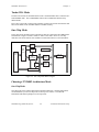
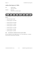
Chapter 2
TNT4882 Architectures
This chapter discusses the internal hardware architectures of the TNT4882.
The TNT4882 has three different internal hardware architectures: one-chip mode,
Turbo+7210 mode, and Turbo+9914 mode. The architecture determines which set of
registers is available to the host interface, the behavior of the bits in the registers, and
how the FIFOs interface to the GPIB.
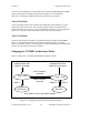
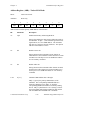
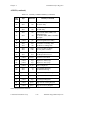
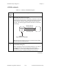
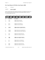
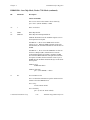
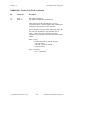
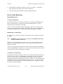
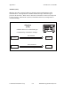
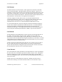
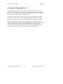
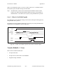
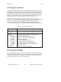
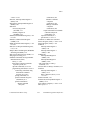
Turbo+7210 Mode
In Turbo+7210 mode, the TNT4882 behaves like a Turbo488 ASIC that is connected to a
NAT4882BPL ASIC. The NAT4882BPL behaves like a µPD7210 that has many
enhancements.
To write data to the GPIB, the host interface writes the data to the FIFOs of the
TNT4882. A transfer state machine transfers the data from the FIFOs to the NAT4882
circuitry, then the NAT4882 circuitry sends the data across the GPIB.
To read data from the GPIB, the NAT4882 circuitry reads data bytes from the GPIB. The
transfer state machine transfers the data from the NAT4882 circuitry to the FIFOs, then
the host interface reads the data from the FIFOs.
Turbo488 Circuitry
Read/
Write
Control
Byte
Counter
Transfer
State
Machine
Read/
Write
Control
GPIB
Data
Registers
IEEE 488
Interface
Functions
Configuration
and
Status Registers
Configuration
and
Status Registers
Local GPIB Signals
ISA
Interface
Logic
NAT4882 Circuitry
NAT4882
Interface
Circuitry
FIFOs
IEEE 488
Transceivers
GPIB
Timer
Interrupt Control
Interrupt Control
IEEE 488 Monitor
Figure 2-1. Turbo+7210 or Turbo+9914 Mode Block Diagram
© National Instruments Corp.
2-1
TNT4882 Programmer Reference
TNT4882 Architectures
Chapter 2
Turbo+9914 Mode
In Turbo+9914 mode, the TNT4882 behaves like a Turbo488 ASIC that is connected to a
NAT4882BPL ASIC. The NAT4882BPL behaves like a TMS9914A that has many
enhancements.
Like Turbo+7210 mode, a transfer state machine in Turbo+9914 mode must transfer data
between the FIFOs of the TNT4882 and the NAT4882 circuitry.
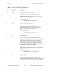
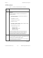
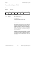
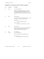
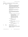
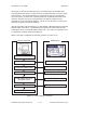
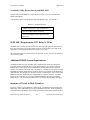
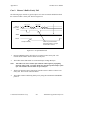
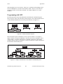
One-Chip Mode
In one-chip mode, the FIFOs of the TNT4882 are directly connected to the GPIB and the
TNT4882 has a register set that is similar to Turbo+7210 mode. However, one-chip
mode does not need a transfer state machine to transfer data either to or from the FIFOs.
FIFOs
Byte
Counter
IEEE 488 Monitor
IEEE 488
Transceivers
IEEE 488
Interface
Functions
Configuration
and
Status Registers
IEEE 488 Bus
ISA
Interface
Logic
Read/
Write
Control
HS488
Interface
Functions
Timer
Interrupt Control
Figure 2-2. One-Chip Mode Block Diagram
Choosing a TNT4882 Architecture Mode
One-Chip Mode
One-chip mode is the simplest and fastest TNT4882 architecture. National Instruments
recommends that you use one-chip mode to develop new software. The National
Instruments ESP-488TL package uses one-chip mode.
TNT4882 Programmer Reference
2-2
© National Instruments Corp.
Chapter 2
TNT4882 Architectures
You can use the TNT4882 in one-chip mode without using the HS488 high-speed GPIB
protocol, but HS488 is available only when the TNT4882 is in one-chip mode.
Therefore, you cannot use HS488 in Turbo+9914 and Turbo+7210 mode.
Turbo+9914 Mode
If you are porting code that was written for the TMS9914A to the TNT4882, you may
want to use Turbo+9914 mode. The 7210-style registers used in one-chip mode are
similar to the 9914-style registers, so it is not difficult to port code to use one-chip mode.
However, you may feel more comfortable if you use the 9914-style registers.
Turbo+7210 Mode
In Turbo+7210 mode, the TNT4882 is compatible with the Turbo488+NAT4882BPL
chip set: only applications written for this chip set should use Turbo+7210 mode.
Turbo+7210 mode is similar to one-chip mode, so National Instruments recommends that
you use one-chip mode to develop new software.
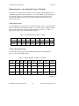
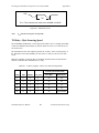
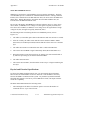
Changing the TNT4882 Architecture Modes
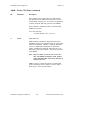
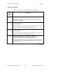
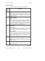
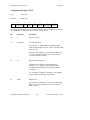
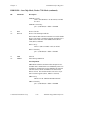
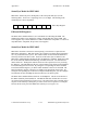
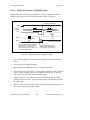
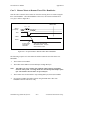
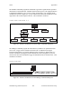
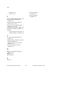
Figure 2-3 shows how you change the TNT4882 architecture modes.
Hardware Reset while
Mode Pin Grounded
Hardware Reset while
Mode Pin Unconnected
sw7210 auxiliary
command
Turbo + 9914
Turbo + 7210
sw9914 auxiliary
command
ONEC=1
Illegal.
Don't do this
ONEC=0
ONEC=1
One Chip
Note: ONEC is bit 0 of the HSSEL Register
Figure 2-3. Changing the Three TNT4882 Architecture Modes
© National Instruments Corp.
2-3
TNT4882 Programmer Reference
TNT4882 Architectures
Chapter 2
Architecture After a Hardware Reset
During a hardware reset, the TNT4882 examines the level of the MODE pin. Generally,
the MODE pin is either connected to logic ground or unconnected. If the MODE pin is
unconnected, an internal pull-up resistor pulls the MODE pin to a logic high level. If the
MODE pin is at a logic low level during a hardware reset, the TNT4882 enters
Turbo+9914 mode. If the MODE pin is at a logic high level during a hardware reset, the
TNT4882 enters Turbo+7210 mode.
Changing between Turbo+9914 Mode and Turbo+7210 Mode
After the hardware reset, the host interface can change the TNT4882 from Turbo+9914
mode to Turbo+7210 mode by writing the sw7210 auxiliary command to the Accessory
Read Register (ACCR). The host interface can change the TNT4882 from Turbo+7210
mode to Turbo+9914 mode by writing the sw9914 auxiliary command to the Auxiliary
Mode Register (AUXMR).
Changing between One-Chip Mode and Turbo+7210 Mode
The host interface can change the TNT4882 from Turbo+7210 mode to one-chip mode by
writing a 1 to the One Chip (ONEC) bit of the Handshake Select Register (HSSEL[0]).
The host interface can change the TNT4882 from one-chip mode to Turbo+7210 mode by
writing a 0 to ONEC.
TNT4882 Programmer Reference
2-4
© National Instruments Corp.
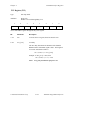
Chapter 3
TNT4882 Interface Registers
This chapter contains TNT4882 address maps and a detailed description of the TNT4882
interface registers.
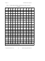
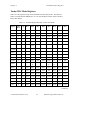
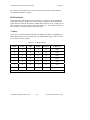
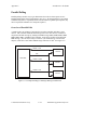
One-Chip Mode/Turbo+7210 Mode Registers
Table 3-1 is the register bit map for the TNT4882 in one-chip mode and Turbo+7210
mode.
© National Instruments Corp.
3-1
TNT4882 Programmer Reference
TNT4882 Interface Registers
Chapter 3
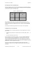
Table 3-1. TNT4882 Register Bit Map: One-Chip Mode and Turbo+7210 Mode
Register
Offset Type
(hex)
Bit 7
Bit 6
Bit 5
Bit 4
Bit 3
Bit 2
Bit 1
Bit 0
DIR
0
R
DIO8
DIO7
DIO6
DIO5
DIO4
DIO3
DIO2
DIO1
CDOR
0
W
DIO8
DIO7
DIO6
DIO5
DIO4
DIO3
DIO2
DIO1
ISR1
2
R
CPT
APT
DET
END RX
DEC
ERR
DO
DI
IMR1
2
W
CPT IE
APT IE
DET IE
END IE
DEC IE
ERR IE
DO IE
DI IE
ISR2
4
R
INT
X
LOK
REM
X
LOKC
REMC
ADSC
IMR2
4
W
0
0
DMAO
DMAI
0
LOKC
IE
REMC
IE
ADSC
IE
ACCWR*
5
W
0
0
0
0
0
0
0
DMAEN
SPSR
6
R
S8
PEND
S6
S5
S4
S3
S2
S1
SPMR
6
W
S8
rsv /
RQS
S6
S5
S4
S3
S2
S1
INTR *
7
W
0
0
0
0
0
0
0
INTEN
ADSR
8
R
X
ATN*
SPMS
LPAS
TPAS
LA
TA
MJMN
ADMR
8
W
ton
lon
1
1
0
0
ADM1
ADM0
CNT2
9
R/W
CNT23
CNT22
CNT21
CNT20
CNT19
CNT18
CNT17
CNT16
CPTR
A
R
CPT7
CPT6
CPT5
CPT4
CPT3
CPT2
CPT1
CPT0
AUXMR
A
W
AUX7
AUX6
AUX5
AUX4
AUX3
AUX2
AUX1
AUX0
CNT3
B
R/W
CNT31
CNT30
CNT29
CNT28
CNT27
CNT26
CNT25
CNT24
ADR0
C
R
X
DT0
DL0
AD5-0
AD4-0
AD3-0
AD2-0
AD1-0
ADR
C
W
ARS
DT
DL
AD5
AD4
AD3
AD2
AD1
HSSEL
D
W
0
0
GO2
SIDS
NO DMA
0
0
0
ONEC
ADR1
E
R
EOI
DT1
DL1
AD5-1
AD4-1
AD3-1
AD2-1
AD1-1
EOSR
E
W
EOS7
EOS6
EOS5
EOS4
EOS3
EOS2
EOS1
EOS0
STS1
10
R
DONE
0
IN
DRQ
STOP
DAV
HALT
GSYNC
CFG
10
W
0
TLC
HLTE
IN
A/BN
CCEN
TMOE
TIM/
BYTN
16/8N
DSR
11
R
DIO8
DIO7
DIO6
DIO5
DIO4
DIO3
DIO2
DIO1
(continues)
TNT4882 Programmer Reference
3-2
© National Instruments Corp.
Chapter 3
TNT4882 Interface Registers
Table 3-1. TNT4882 Register Bit Map: One-Chip Mode and Turbo+7210 Mode
(Continued)
Register
Offset Type
(hex)
Bit 7
Bit 6
Bit 5
Bit 4
Bit 3
Bit 2
Bit 1
Bit 0
SH_CNT
11
W
CNT2
CNT1
CNT0
TD4
TD3
TD2
TD1
TD0
IMR3
12
R/W
0
INTSRC2
IE
0
STOP IE
NFF IE
NEF IE
TLC
INT IE
DONE
IE
HIER
13
W
DGA
DGB
0
NO_
TSETUP
0
0
0
PMT_
W_ EOS
CNT0
14
R/W
CNT7
CNT6
CNT5
CNT4
CNT3
CNT2
CNT1
CNT0
MISC
15
W
0
0
0
HSE
SLOW
WRAP
NOAS
NOTS
CNT1
16
R/W
CNT15
CNT14
CNT13
CNT12
CNT11
CNT10
CNT9
CNT8
CSR
17
R
V3
V2
V1
V0
KEY
DQ
MODE
0
0
KEYREG
17
W
0
SWAP
0
0
KEY
CLK
KEY
DAT
EN
KEY
DATA
KEY
RST*
FIFOB
18
R/W
FB7
FB6
FB5
FB4
FB3
FB2
FB1
FB0
FIFOA
19
R/W
FA15
FA14
FA13
FA12
FA11
FA10
FA9
FA8
ISR3
1A
R
INT
INTSRC
2
X
STOP
NFF
NEF
TLC
INT
DONE
CCR
1A
W
D7
D6
D5
D4
D3
D2
D1
D0
SASR
1B
R
nba
AEHS
ANHS1
ANHS2
ADHS
ACRDY
SH1A
SH1B
DCR
1B
W
DIO8
DIO7
DIO6
DIO5
DIO4
DIO3
DIO2
DIO1
STS2
1C
R
1
16/8N
0
1
AFFN
AEFN
BFFN
BEFN
CMDR
1C
W
CMD7
CMD6
CMD5
CMD4
CMD3
CMD2
CMD1
CMD0
ISR0
1D
R
nba
STBO
NL
EOS
IFCI
ATNI
TO
SYNC
IMR0
1D
W
1
STBO
IE
NLEN
BTO
IFCI IE
ATNI
IE
TO IE
SYNC
IE
TIMER
1E
R/W
TMR7
TMR6
TMR5
TMR4
TMR3
TMR2
TMR1
TMR0
BSR
1F
R
ATN
DAV
NDAC
NRFD
EOI
SRQ
IFC
REN
BCR
1F
W
ATN
DAV
NDAC
NRFD
EOI
SRQ
IFC
REN
* These registers are accessible only in the ISA pin configuration.
© National Instruments Corp.
3-3
TNT4882 Programmer Reference
TNT4882 Interface Registers
Chapter 3
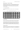
Hidden Registers: One-Chip Mode/Turbo+7210 Mode
In addition to the registers shown in Table 3-1, the TNT4882 contains hidden registers.
All hidden registers are write-only registers. Two or more hidden registers can appear at
the same offset. When you write an 8-bit pattern to these offsets, some of the bits
determine the hidden register that will be written; the other bits represent the value
written to the register.
Address Register Map
The TNT4882 has two address registers: ADR1 and ADR0. Table 3-1 shows the offsets
for the readable portion of ADR1 and ADR0. The writable portion of ADR0 and ADR1
appears at the offset of the Address Register (ADR) shown in Table 3-1. Table 3-2
shows the bit map for the two writable address registers.
Table 3-2. Hidden Registers at Offset C (ADR)
Register
Bit 7
Bit 6
Bit 5
Bit 4
Bit 3
Bit 2
Bit 1
Bit 0
ADR0
0
DT0
DL0
AD5-0
AD4-0
AD3-0
AD2-0
AD1-0
ADR1
1
DT1
DL1
AD5-1
AD4-1
AD3-1
AD2-1
AD1-1
Auxiliary Mode Register Map
Several hidden registers appear at the Auxiliary Mode Register (AUXMR) offset.
Table 3-3 shows these hidden registers.
Table 3-3. Hidden Registers at Offset A (AUXMR)
Register
Bit 7
Bit 6
Bit 5
Bit 4
Bit 3
Bit 2
Bit 1
Bit 0
PPR
0
1
1
U
S
P3
P2
P1
AUXRA
1
0
0
BIN
XEOS
REOS
HLDE
HLDA
AUXRB
1
0
1
ISS
0
TRI
SPEOI
CPT
ENABLE
AUXRE
1
1
0
0
DHADT
DHADC
DHDT
DHDC
(continues)
TNT4882 Programmer Reference
3-4
© National Instruments Corp.
Chapter 3
TNT4882 Interface Registers
Table 3-3. Hidden Registers at Offset A (AUXMR) (Continued)
Register
Bit 7
Bit 6
Bit 5
Bit 4
Bit 3
Bit 2
Bit 1
Bit 0
AUXRF
1
1
0
1
DHATA
DHALA
DHUNTL
DHALL
AUXRG
0
1
0
0
NTNL
0
0
CHES
AUXRI
1
1
1
0
USTD
PP2
0
SISB
AUXRJ
1
1
1
1
TM3
TM2
TM1
TM0
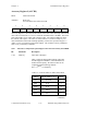
SH_CNT Map
Several hidden registers appear at the SH_CNT offset. Table 3-4 shows these hidden
registers.
Table 3-4. Register Map of the SH_CNT Register
Register
Type
Bit 7
Bit 6
Bit 5
Bit 4
Bit 3
Bit 2
Bit 1
Bit 0
PT1
W
0
0
PT1_
ENA
PT1_4
PT1_3
PT1_2
PT1_1
PT1_0
T17
W
0
1
0
T17_4
T17_3
T17_2
T17_1
T17_0
T12
W
1
0
0
T12_4
T12_3
T12_2
T12_1
T12_0
T13
W
1
1
0
T13_ 4
T13_3
T13_2
T13_ 1
T13_0
The Page-In State (One-Chip Mode/Turbo+7210 Mode)
The TNT4882 implements a Page-In state to be compatible with designs that assume the
TNT4882 ASIC is used in 7210 mode. When the Page-In state is true, several registers
are mapped to different locations and other registers are not accessible at any offset.
When to Use the Page-In State
New software should not use the Page-In state. Only applications that require complete
software compatibility with the Turbo488 and NAT4882 ASICs should use the Page-In
state.
© National Instruments Corp.
3-5
TNT4882 Programmer Reference
TNT4882 Interface Registers
Chapter 3
How to Page-In
The TNT4882 enters the Page-In state when the host interface writes the Page-In
auxiliary command to the AUXMR. The TNT4882 registers appear at their Page-In state
offset for the first register access after the Page-In command. The TNT4882 leaves the
Page-In state at the end of the first register access after the Page-In command. The
TNT4882 also enters the Page-In state when the PAGE pin of the TNT4882 is asserted.
The TNT4882 exits the Page-In state when the PAGE pin is unasserted. See Table 3-5.
Table 3-5. One-Chip Mode and Turbo+7210 Mode Page-In State Register Offsets
Register
Type
Normal Offset
(Hex)
Page-In State
Offset (Hex)
SPSR
R
6
Not Accessible
SPMR
W
6
Not Accessible
CPTR
R
A
Not Accessible
ADR0
R
C
Not Accessible
ADR
W
C
Not Accessible
ADR1
R
E
Not Accessible
EOSR
W
E
Not Accessible
CSR
R
17
6
KEYREG
W
17
6
SASR
R
1B
A
ISR0
R
1D
C
IMR0
W
1D
C
BSR
R
1F
E
BCR
W
1F
E
TNT4882 Programmer Reference
3-6
© National Instruments Corp.
Chapter 3
TNT4882 Interface Registers
Turbo+9914 Mode Registers
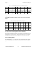
Table 3-6 is the register bit map for the TNT4882 in Turbo+9914 mode. The offsets in
Table 3-6 assume that the SWAP bit is set. See The SWAP Bit section, which is located
later in this chapter.
Table 3-6. TNT4882 Register Bit Map: Turbo+9914 Mode
Register
Offset Type
(hex)
Bit 7
Bit 6
Bit 5
Bit 4
Bit 3
Bit 2
Bit 1
Bit 0
DIR
0
R
DIO8
DIO7
DIO6
DIO5
DIO4
DIO3
DIO2
DIO1
CDOR
0
W
DIO8
DIO7
DIO6
DIO5
DIO4
DIO3
DIO2
DIO1
CPTR
2
R
CPT7
CPT6
CPT5
CPT4
CPT3
CPT2
CPT1
CPT0
PPR
2
W
PP8
PP7
PP6
PP5
PP4
PP3
PP2
PP1
SPSR †
4
R
S8
PEND
S6
S5
S4
S3
S2
S1
SPMR
4
W
S8
rsv/
RQS
S6
S5
S4
S3
S2
S1
ACCWR*
5
W
0
0
0
0
0
0
0
DMAEN
ISR2†
6
R
nba
STBO
NL
EOS
LLOC
ATNI
TO
0
ADR
6
W
edpa
dal
dat
A5
A4
A3
A2
A1
INTR *
7
W
0
0
0
0
0
0
0
INTEN
ADSR
8
R
REM
LLO
ATN
LPAS
TPAS
LA
TA
ulpa
IMR2†
8
W
1
STBO
IE
NLEN
BTO
LLOC
IE
ATNI
IE
TO IE
0
EOSR†
8
W
EOS7
EOS6
EOS5
EOS4
EOS3
EOS2
EOS1
EOS0
BCR†
8
W
ATN
DAV
NDAC
NRFD
EOI
SRQ
IFC
REN
ACCR†
8
W
ACC7
ACC6
ACC5
ACC4
ACC3
ACC2
ACC1
ACC0
CNT2
9
R/W
CNT23
CNT22
CNT21
CNT20
CNT19
CNT18
CNT17
CNT16
BSR
A
R
ATN
DAV
NDAC
NRFD
EOI
SRQ
IFC
REN
AUXCR
A
W
C/S
0
0
F4
F3
F2
F1
F0
CNT3
B
R/W
CNT31
CNT30
CNT29
CNT28
CNT27
CNT26
CNT25
CNT24
(continues)
© National Instruments Corp.
3-7
TNT4882 Programmer Reference
TNT4882 Interface Registers
Chapter 3
Table 3-6. TNT4882 Register Bit Map: Turbo+9914 Mode (Continued)
Register
Offset Type
(hex)
Bit 7
Bit 6
Bit 5
Bit 4
Bit 3
Bit 2
Bit 1
Bit 0
ISR0
C
R
INT0
INT1
BI
BO
END
SPAS
RLC
MAC
IMR0
C
W
DMAO
DMAI
BI IE
BO IE
END IE
SPAS
IE
RLC IE
MAC IE
HSSEL
D
W
0
0
GO2
SIDS
NODMA
0
0
0
ONEC
ISR1
E
R
GET
ERR
UNC
APT
DCAS
MA
X
IFC
IMR1
E
W
GET IE
ERR IE
UNC IE
APT IE
DCAS
IE
MA IE
0
IFC IE
STS1
10
R
DONE
0
IN
DRQ
STOP
DAV
HALT
GSYNC
CFG
10
W
0
TLC
HLTE
IN
A/BN
CCEN
TMOE
TIM/
BYTN
16/8N
IMR3
12
R/W
0
INT
SRC2
IE
0
STOP IE
NFF IE
NEF IE
TLC
INT IE
DONE
IE
HIER
13
W
DGA
DGB
0
NO_
TSETUP
0
0
0
PMT_
W_ EOS
CNT0
14
R/W
CNT7
CNT6
CNT5
CNT4
CNT3
CNT2
CNT1
CNT0
CNT1
16
R/W
CNT15
CNT14
CNT13
CNT12
CNT11
CNT10
CNT9
CNT8
FIFOB
18
R/W
FB7
FB6
FB5
FB4
FB3
FB2
FB1
FB0
FIFOA
19
R/W
FA15
FA14
FA13
FA12
FA11
FA10
FA9
FA8
ISR3
1A
R
INT
INT
SRC2
0
STOP
NFF
NEF
TLC
INT
DONE
CCR
1A
W
D7
D6
D5
D4
D3
D2
D1
D0
STS2
1C
R
1
16/8N
0
1
AFFN
AEFN
BFFN
BEFN
CMDR
1C
W
CMD7
CMD6
CMD5
CMD4
CMD3
CMD2
CMD1
CMD0
TIMER
1E
R/W
TMR7
TMR6
TMR5
TMR4
TMR3
TMR2
TMR1
TMR0
* These registers are accessible only in the ISA pin configuration.
† Page-In registers. See Turbo+9914 Page-In State.
TNT4882 Programmer Reference
3-8
© National Instruments Corp.
Chapter 3
TNT4882 Interface Registers
Hidden Registers: Turbo+9914 Mode
In addition to the registers shown above, the TNT4882 contains hidden registers. All
hidden registers are write-only registers. Two or more hidden registers can appear at
the same offset. When you write an 8-bit pattern to these offsets, some of the bits
determine the hidden register that will be written; the other bits represent the value
written to the register.
Accessory Read Register Map
Several hidden registers appear at the ACCR offset. Table 3-7 shows these hidden
registers.
Table 3-7. Hidden Registers at the ACCR Offset
Register
Bit 7
Bit 6
Bit 5
Bit 4
Bit 3
Bit 2
Bit 1
Bit 0
ACCRA
1
0
0
BIN
XEOS
REOS
0
0
ACCRB
1
0
1
ISS
0
0
SPEOI
0
ACCRE
1
1
0
0
DHADT
DHADC
0
0
ACCRF
1
1
0
1
DHATA
DHALA
DHUNTL
DHALL
ACCRI
1
1
1
0
USTD
PP1
0
DMAE
ACCRJ
1
1
1
1
TM3
TM2
TM1
TM0
The SWAP Bit
The offsets of some Turbo+9914 mode registers depend on the value of the SWAP bit.
SWAP does not affect the offsets of Turbo+7210 mode or one-chip mode registers.
In Turbo+9914 mode, the TNT4882 transfer state machine moves data between the
FIFOs and the TNT4882 circuitry. The transfer state machine assumes that the Data
In Register (DIR) and the Command/Data Out Register (CDOR) are located at offset 0.
In Turbo+9914 mode, however, the DIR and CDOR are located at offset 0 only if
SWAP = 1. If the FIFOs will be used in Turbo+9914 mode, the SWAP bit should be 1.
Setting the SWAP Bit
During a hardware reset, the TNT4882 samples the logic value on the SWAPN pin. If
SWAPN is low during a hardware reset, the SWAP bit is set. If SWAPN is high during a
hardware reset, the SWAP bit is cleared. You can also set or clear the SWAP bit by
© National Instruments Corp.
3-9
TNT4882 Programmer Reference
TNT4882 Interface Registers
Chapter 3
writing to the Key Control Register (KCR). KCR is accessible only when the TNT4882
is in Turbo+7210 mode or one-chip mode.
Note:
If you use the TNT4882 in the ISA pin configuration, the SWAPN pad is not
accessible external to the chip but is internally shorted to the MODE pin.
Thus, in ISA pin configuration, if the MODE pin is asserted during a
hardware reset, the TNT4882 powers up in Turbo+9914 mode with the SWAP
bit set.
Recommendation
For applications that use Turbo+9914 mode, National Instruments recommends that the
SWAP bit is set in Turbo+9914 mode. The easiest way to implement a Turbo+9914
mode application is to connect the MODE pin and SWAPN pin to ground.
The Page-In Condition (Turbo+9914 Mode)
Four writable registers can appear at the same offset as the Address Status Register
(offset 4 if SWAP = 0; offset 8 if SWAP = 1). After a hardware or software reset, no
writable register appears at the Address Status Register (ADSR) offset; the TNT4882
ignores writes to that offset.
One Page-In auxiliary command exists for each of the four registers. The host interface
can make one of the four registers accessible by issuing the appropriate Page-In
command to the Auxiliary Command Register (AUXCR). The paged-in register remains
accessible at the ADSR offset until the host interface either pages-in another register or
issues the Clear Page-In Register auxiliary command.
When any one of the four writable registers is accessible at the ADSR offset, Interrupt
Status Register 2 (ISR2) is accessible at the same offset as the ADR, and the Serial Poll
Status Register (SPSR) is accessible at the same offset as the Serial Poll Mode Register
(SPMR).
Register Bit Descriptions
8-Bit Versus 16-Bit Accesses
All TNT4882 registers are 8-bit registers. However, by making a 16-bit access to the
same offset as FIFO B, the host interface can access FIFO A and FIFO B simultaneously
to form a 16-bit register.
TNT4882 Programmer Reference
3-10
© National Instruments Corp.
Chapter 3
TNT4882 Interface Registers
9914 and 7210 Registers with Identical Names
Some registers are accessible only in Turbo+9914 mode and some registers are accessible
only in Turbo+7210 mode or one-chip mode. Some registers are accessible in several
modes, but their bits have completely different meanings. Make sure you read the bit
descriptions that are appropriate for the mode your application uses.
All registers are listed in alphabetical order. The registers are alphabetized according to
their mnemonics.
© National Instruments Corp.
3-11
TNT4882 Programmer Reference
TNT4882 Interface Registers
Chapter 3
Accessory Register A (ACCRA)
Mode:
Turbo+9914 mode
Attributes:
Write only
Accessed at the same offset as ACCR
7
6
5
4
3
2
1
0
1
0
0
BIN
XEOS
REOS
0
0
Accessory Register A (ACCRA) controls the EOS and END messages. A ch_rst
auxiliary command or a hardware reset clears ACCRA.
Bit
Mnemonic
Description
4w
BIN
Binary bit
The BIN bit selects the length of the EOS message. If
BIN = 1, the EOSR is treated as an 8-bit byte. When
BIN = 0, the EOSR is treated as a 7-bit register (for
ASCII characters), and only a 7-bit comparison is done
with the data on the GPIB.
3w
XEOS
Transmit END With EOS bit
The XEOS bit permits or prohibits automatic transmission
of the GPIB END message at the same time as the EOS
message when the TNT4882 is in Talker Active State
(TACS). If XEOS = 1 and the byte in the CDOR matches
the contents of the EOSR, the EOI line is sent true along
with the data.
2w
REOS
END On EOS Received bit
The REOS bit permits or prohibits setting the END bit
(ISR0[3]r) when the TNT4882 receives the EOS message
as a Listener. If REOS = 1 and the byte in the DIR
matches the byte in the EOSR, the END bit is set and the
acceptor function treats the EOS character just as if it
were received with EOI asserted.
TNT4882 Programmer Reference
3-12
© National Instruments Corp.
Chapter 3
TNT4882 Interface Registers
Accessory Register B (ACCRB)
Mode:
Turbo+9914 mode
Attributes:
Write only
Accessed at the same offset as ACCR
7
6
5
4
3
2
1
0
1
0
1
ISS
0
0
SPEOI
0
Bit
Mnemonic
Description
4w
ISS
Individual Status Select bit
ISS determines the value of the TNT4882 ist message.
When ISS = 1, ist takes on the value of the TNT4882
SRQS. (The TNT4882 is asserting the GPIB SRQ
message when it is in SRQS.) If ISS = 0, ist takes on the
value of the TNT4882 Parallel Poll Flag. You set and
clear the Parallel Poll Flag by using the Set Parallel Poll
Flag and Clear Parallel Poll Flag auxiliary commands.
1w
SPEOI
Send Serial Poll EOI bit
SPEOI permits or prohibits the transmission of the END
message in SPAS. If SPEOI = 1, EOI is sent true when
the TNT4882 is in SPAS and is sourcing an STB.
Otherwise, EOI is sent false in SPAS.
© National Instruments Corp.
3-13
TNT4882 Programmer Reference
TNT4882 Interface Registers
Chapter 3
Accessory Register E (ACCRE)
Mode:
Turbo+9914 mode
Attributes:
Write only
Accessed at the same offset as ACCR
7
6
5
4
3
2
1
0
1
1
0
0
DHADT
DHADC
0
0
Accessory Register E (ACCRE) determines how the TNT4882 uses a Data Accepted
(DAC) holdoff. A ch_rst auxiliary command or a hardware reset clears ACCRE.
Each bit of ACCRE enables DAC holdoffs on a GPIB command or group of commands.
When a GPIB Controller sends the specified command to the TNT4882, the CPT bit sets
and the TNT4882 performs a DAC holdoff. See the DAC Holdoffs section in Chapter 4,
TNT4882 Programming Considerations.
Bit
Mnemonic
Description
3w
DHADT
DAC Holdoff On GET bit
2w
DHADC
DAC Holdoff On DCL Or SDC bit
TNT4882 Programmer Reference
3-14
© National Instruments Corp.
Chapter 3
TNT4882 Interface Registers
Accessory Register F (ACCRF)
Mode:
Turbo+9914 mode
Attributes:
Write only
Accessed at the same offset as ACCR
7
6
5
4
1
1
0
1
3
2
DHATA DHALA
1
0
DHUNTL
DHALL
Accessory Register F (ACCRF) determines how the TNT4882 uses a DAC holdoff.
A ch_rst auxiliary command or a hardware reset clears ACCRF.
Each bit of ACCRF enables DAC holdoffs on a GPIB command or group of commands.
When a GPIB Controller sends the specified command to the TNT4882, the CPT bit sets
and the TNT4882 performs a DAC holdoff. See the DAC Holdoffs section in Chapter 4,
TNT4882 Programming Considerations.
Bit
Mnemonic
Description
3w
DHATA
DAC Holdoff On All Talker Addresses bit
2w
DHALA
DAC Holdoff On All Listener Addresses bit
1w
DHUNTL
DAC Holdoff On The UNT Or UNL Command bit
0w
DHALL
DAC Holdoff On All UCG, ACG, And SCG Commands
bit
© National Instruments Corp.
3-15
TNT4882 Programmer Reference
TNT4882 Interface Registers
Chapter 3
Accessory Register I (ACCRI)
Mode:
Turbo+9914 mode
Attributes:
Write only
Accessed at the same offset as ACCR
7
6
5
4
3
2
1
0
1
1
1
0
USTD
PP1
0
DMAE
Bit
Mnemonic
Description
3w
USTD
Ultra Short T1 Delay bit
If USTD = 1, the T1 delay can be as short as 350 ns. See
the T1 Delay Generation section in Chapter 4, TNT4882
Programming Considerations.
2w
PP1
Parallel Poll bit 1
The PP1 bit permits or prohibits the TNT4882's ability
to automatically respond to remote parallel poll
configuration. If PP1 = 1, the interface can be configured
remotely for parallel polls.
The Acceptor Handshake does not perform a DAC
holdoff or set the UNC bit when it receives a Parallel Poll
Command (PPC or PPU).
If PP1 = 0, parallel polls must be configured through the
PPR, and Parallel Poll commands must be monitored by
UNC.
0w
DMAE
DMA Enable bit
If you use the FIFOs for data transfers, set DMAE. For
GPIB reads, also set DMAI in IMR0. For GPIB writes,
also set DMAO in IMR0.
TNT4882 Programmer Reference
3-16
© National Instruments Corp.
Chapter 3
TNT4882 Interface Registers
Accessory Register J (ACCRJ)
Mode:
Turbo+9914 mode
Attributes:
Write only
Accessed at the same offset as ACCR
7
6
5
4
3
2
1
0
1
1
1
1
TM3
TM2
TM1
TM0
Accessory Register J (ACCRJ) sets the timeout value of the Timer interrupt. The timeout
value can be set between 15 µs to 125 s when the TNT4882 clock is 40 MHz. The Timer
starts when TM[3–0] are written with a nonzero value. The TO bit in ISR2 sets when
the timeout value expires. The Timer is cleared when a 0 is written to TM[3–0]. For
more information on the Timer interrupt capability, see the Interrupt Status Register 2
(ISR2)—Turbo+9914 Mode section in this chapter. The ACCRJ is reset by a hardware
reset or a ch_rst auxiliary command.
Note:
This timer is independent of the DRQ assertion timer described by the TIMER.
Bit
Mnemonic
Description
3–0w
TM[3–0]
Timer bits 3 through 0
Table 3-8 lists the approximate timeout values that
ACCRJ supports at 40 MHz. If the TNT4882 uses
another clock frequency, the timeout value can be
computed with the following formula:
time = (2factor * 5)/frequency.
Table 3-8. Timeout Values in Turbo+9914 Mode
TM3–0
Timeout Value (> or =)
Factor
0000
Disabled
–
0001
16 µs
7
0010
32 µs
8
0011
128 µs
10
0100
256 µs
11
(continues)
© National Instruments Corp.
3-17
TNT4882 Programmer Reference
TNT4882 Interface Registers
Chapter 3
ACCRJ (continued)
Table 3-8. Timeout Values in Turbo+9914 Mode
(Continued)
TM3–0
Timeout Value (> or =)
Factor
0101
1 ms
13
0110
4 ms
15
0111
16 ms
17
1000
33 ms
18
1001
131 ms
20
1010
262 ms
21
1011
1s
23
1100
4s
26
1101
17 s
27
1110
34 s
28
1111
134 s
30
Depending on the value of the BTO bit, IMR2[4]w, the Timer works with two different
types of timeouts. If BTO = 0, the Timer starts when the host interface writes a
nonzero value to the Timer Register. When the Timer reaches the timeout value, it sets
the TO bit.
If BTO = 1, the Timer operates in byte timeout mode. In this mode, the Timer starts
when the host interface writes a nonzero value to the Timer Register. The Timer counts
until it reaches the timeout value. However, reads of the DIR or writes of the CDOR
clear the Timer and force it to begin counting again. If TO is set in byte timeout mode, it
remains set until the Timer Register is written. Further reads of DIR or writes of CDOR
have no effect on TO until the Timer Register is written.
TNT4882 Programmer Reference
3-18
© National Instruments Corp.
Chapter 3
TNT4882 Interface Registers
Accessory Write Register (ACCWR)
Type:
All modes
ISA pin configuration only
Attributes:
Write only
7
6
5
4
3
2
1
0
0
0
0
0
0
0
0
DMAEN
Bit
Mnemonic
Description
7–1w
0
Write 0 to these bits.
0w
DMAEN
DMA Enable bit
When DMAEN = 0, the TNT4882 tristates the DRQ pin
and ignores the DACKN pin. When DMAEN = 1, the
TNT4882 responds to DMA accesses and drives DRQ
high or low. The host interface should set DMAEN at the
beginning of a DMA transfer, before the host interface
enables the DMA controller. The host interface should
clear DMAEN at the completion of a DMA transfer.
A hardware reset clears DMAEN.
© National Instruments Corp.
3-19
TNT4882 Programmer Reference
TNT4882 Interface Registers
Chapter 3
Address Mode Register (ADMR)
Type:
One-chip mode
Turbo+7210 mode
Attributes:
Write only
7
6
5
4
3
2
1
0
ton
lon
1
1
0
0
ADM1
ADM0
The host interface can put the TNT4882 into one of six GPIB addressing modes by
writing to the Address Mode Register (ADMR). The value of the ADMR is undefined
after a hardware reset. Before the host interface can clear pon, it must write a valid
pattern to the ADMR. All values not defined in the following table are reserved.
Table 3-9. Valid ADMR Patterns
Hex Value
of ADMR
30
GPIB Addressing Mode
No Addressing
The Controller cannot address the TNT4882 to become a Talker or
Listener in no-addressing mode.
31
Normal Dual Addressing
The TNT4882 can implement one or two logical devices by using
normal dual addressing.
See the GPIB Addressing section in Chapter 4, TNT4882 Programming
Considerations.
32
Extended Single Addressing
Extended single addressing mode implements the Extended Listener and
Extended Talker functions, as defined in the IEEE 488 standard, without
intervention from the host interface.
See the GPIB Addressing section in Chapter 4, TNT4882 Programming
Considerations.
(continues)
TNT4882 Programmer Reference
3-20
© National Instruments Corp.
Chapter 3
TNT4882 Interface Registers
ADMR (continued)
Table 3-9. Valid ADMR Patterns (Continued)
Hex Value
of ADMR
33
GPIB Addressing Mode
Extended Dual Addressing
Extended dual addressing mode implements the Extended Listener and
Extended Talker functions, as defined in the IEEE 488 standard. This
mode requires intervention from the host interface.
See the GPIB Addressing section in Chapter 4, TNT4882 Programming
Considerations.
70
Listen Only (lon)
The TNT4882 becomes a GPIB Listener and enters the Listener Active
State (LACS). Do not use lon if a GPIB Controller is present in the
GPIB system.
The host interface should write a hex 30 (No Addressing) to the ADMR
immediately after it writes lon to the ADMR. To force the TNT4882 to
exit LACS, issue the unlisten (lul) auxiliary command.
B0
Talk Only (ton)
The TNT4882 becomes a GPIB Talker. Do not use ton if a GPIB
Controller is present in the GPIB system.
The host interface should write a hex 30 (No Addressing) to the ADMR
immediately after it writes ton to the ADMR. To force the TNT4882 to
exit TACS, issue the local untalk (lut) auxiliary command.
© National Instruments Corp.
3-21
TNT4882 Programmer Reference
TNT4882 Interface Registers
Chapter 3
Address Register (ADR)—One-Chip Mode, Turbo+7210 Mode
Type:
One-chip mode
Turbo+7210 mode
Attributes:
Write only
7
6
5
4
3
2
1
0
ARS
DT
DL
AD5
AD4
AD3
AD2
AD1
Writing to the Address Register (ADR) loads the internal registers ADR0 and ADR1.
You must load both ADR0 and ADR1 for all addressing modes.
Bit
Mnemonic
Description
7w
ARS
Address Register Select bit
If ARS = 1, writing to the ADR loads the seven low-order
bits of ADR into internal register ADR1. If ARS = 0,
writing to the ADR loads the seven low-order bits of ADR
into ADR0.
6w
DT
Disable Talker bit
DT = 1 disables recognition of the GPIB talk address
formed from AD5 through AD1(ADR[4–0]w). ADR0
and ADR1 have independent DT bits.
5w
DL
Disable Listener bit
DL = 1 disables recognition of the GPIB listen address
formed from AD5 through AD1(ADR[4–0]w). ADR0
and ADR1 have independent DL bits.
4–0w
AD[5–1]
TNT4882 GPIB Address bits 5 through 1
These bits specify the GPIB address of the TNT4882.
The corresponding GPIB talk address is formed by adding
hex 40 to AD[5–1], while the corresponding GPIB listen
address is formed by adding hex 20 to AD[5–1]. The
value written to AD[5–1] should not be 11111 (binary),
because the corresponding talk and listen addresses would
conflict with the GPIB Untalk (UNT) and GPIB Unlisten
(UNL) commands.
TNT4882 Programmer Reference
3-22
© National Instruments Corp.
Chapter 3
TNT4882 Interface Registers
Address Register (ADR)—Turbo+9914 Mode
Mode:
Turbo+9914 mode
Attributes:
Write only
7
6
5
4
3
2
1
0
edpa
dal
dat
A5
A4
A3
A2
A1
ADR is used to load the primary GPIB address of the interface.
Bit
Mnemonic
Description
7w
edpa
Enable Dual Primary Addressing Mode bit
Setting edpa enables the dual primary addressing mode of
the TNT4882. If edpa = 1, the TNT4882 ignores the least
significant bit (A1) of its GPIB address. The TNT4882
then has two consecutive primary addresses. The ulpa bit
indicates which address is active.
6w
dal
Disable Listener bit
Setting dal returns the TNT4882 Listener function to
LIDS and forces the TNT4882 Listener function to remain
in LIDS even if the chip receives its GPIB listen address
or a lon auxiliary command.
5w
dat
Disable Talker bit
Setting dat returns the TNT4882 Talker function to TIDS
and forces the Talker function to remain in TIDS even if
the chip receives its GPIB talk address or a ton auxiliary
command.
4–0w
A[5–1]
TNT4882 GPIB Address bits 5 through 1
AD[5–1] specify the primary GPIB address of the
TNT4882. The corresponding GPIB talk address is
formed by adding hex 40 to AD[5–1], while the
corresponding GPIB listen address is formed by adding
hex 20. AD[5–1] should not be 11111 (binary), because
the corresponding talk and listen addresses then conflict
with the GPIB UNT and GPIB UNL commands.
© National Instruments Corp.
3-23
TNT4882 Programmer Reference
TNT4882 Interface Registers
Chapter 3
Address Register 0 (ADR0)
Type:
One-chip mode
Turbo+7210 mode
Attributes:
Read only
7
6
5
4
3
2
1
0
X
DT0
DL0
AD5–0
AD4–0
AD3–0
AD2–0
AD1–0
Address Register 0 (ADR0) reflects the internal GPIB address status of the TNT4882.
In extended single addressing mode, ADR0 indicates the address and enable bits for the
primary GPIB address of the TNT4882. In the dual primary addressing modes, ADR0
indicates the TNT4882 major primary GPIB address. See the GPIB Addressing section in
Chapter 4, TNT4882 Programming Considerations.
Bit
Mnemonic
Description
7r
X
Reads back a 1 or 0.
6r
DT0
Disable Talker 0 bit
If DT0 = 1, the primary (or major) Talker is not enabled,
and this register is not compared with GPIB Talker
addresses.
If DT0 = 0, the TNT4882 responds to a GPIB talk address
matching bits AD[5–0 through 1–0].
5r
DL0
Disable Listener 0 bit
If DL0 = 1, the primary (or major) Listener is not enabled,
and this register is not compared with GPIB Listener
addresses.
If DL0 = 0, the TNT4882 responds to a GPIB listen
address matching bits AD[5–0 through 1–0].
4–0r
AD[5–0 – 1–0]
TNT4882 GPIB Address bits 5–0 through 1–0
These are the lower 5 bits of the TNT4882 GPIB primary
(or major) address. The primary talk address is formed by
adding hex 40 to AD[5–0 through 1–0], while the listen
address is formed by adding hex 20.
TNT4882 Programmer Reference
3-24
© National Instruments Corp.
Chapter 3
TNT4882 Interface Registers
Address Register 1 (ADR1)
Type:
One-chip mode
Turbo+7210 mode
Attributes:
Read only
7
6
5
4
3
2
1
0
EOI
DT1
DL1
AD5–1
AD4–1
AD3–1
AD2–1
AD1–1
Address Register 1 (ADR1) indicates the status of the GPIB address and enable bits for
the secondary address of the TNT4882 if extended single addressing is used. ADR1
indicates the minor primary address of the TNT4882 if dual primary addressing is used.
See the GPIB Addressing section in Chapter 4, TNT4882 Programming Considerations.
Bit
Mnemonic
Description
7r
EOI
End-or-Identify bit
EOI indicates the value of the GPIB EOI line that is
latched when a data byte is received by the TNT4882
GPIB Acceptor Handshake (AH) function. If EOI = 1, the
EOI line was asserted with the received byte. EOI is
cleared by issuing the chip reset auxiliary command. EOI
is updated after each byte is received.
6r
DT1
Disable Talker 1 bit
If DT1 = 1, the secondary (or minor) Talker function is
not enabled—that is, the GPIB secondary address (or
minor primary talk address) is not compared with this
register.
5r
DL1
Disable Listener 1 bit
If DL1 = 1, the secondary (or minor) Listener function is
not enabled—that is, the GPIB secondary address (or
minor primary listen address) is not compared with this
register.
4–0r
AD[5–1 – 1–1]
TNT4882 GPIB Address bits 5–1 through 1–1
These bits indicate the TNT4882 secondary or minor
address. Form the secondary address byadding hex 60 to
bits AD[5–1 through 1–1]. Form the minor talk address
by adding hex 40 to AD[5–1 through 1–1]. Form the
listen address by adding a hex 20.
© National Instruments Corp.
3-25
TNT4882 Programmer Reference
TNT4882 Interface Registers
Chapter 3
Address Status Register (ADSR)—Turbo+7210 Mode
Type:
One-chip mode
Turbo+7210 mode
Attributes:
Read only
7
6
5
4
3
2
1
0
X
ATN*
SPMS
LPAS
TPAS
LA
TA
MJMN
The Address Status Register (ADSR) contains information that you can use to monitor
the TNT4882 GPIB address status.
Bit
Mnemonic
Description
7r
X
Don't care bit
This bit reads as 1 or 0.
6r
ATN*
Attention* bit
ATN* is a status bit that indicates the current level of the
GPIB ATN* signal. If ATN* = 0, the GPIB ATN* signal
is asserted.
5r
SPMS
Serial Poll Mode State bit
If SPMS = 1, the TNT4882 GPIB Talker (T) or Talker
Extended (TE) function is enabled to participate in a serial
poll.
SPMS is set by
SPE & ACDS
SPMS is cleared by
(SPD & ACDS) + pon + IFC
TNT4882 Programmer Reference
3-26
© National Instruments Corp.
Chapter 3
TNT4882 Interface Registers
ADSR—Turbo+7210 Mode (continued)
Bit
Mnemonic
Description
4r
LPAS
Listener Primary Addressed State bit
LPAS indicates that the TNT4882 has received its
primary listen address. See the Address Mode Register
(ADMR) section in this chapter.
LPAS is cleared by
(PCG & ~MLA & ACDS) + pon
3r
TPAS
Talker Primary Addressed State bit
TPAS indicates that the TNT4882 has received its
primary GPIB talk address. See the Address Mode
Register (ADMR) section in this chapter.
TPAS is cleared by
(PCG & ~MTA & ACDS) + pon
2r
LA
Listener Active bit
LA = 1 when the TNT4882 has been addressed or
programmed as a GPIB Listener—that is, the TNT4882 is
in the Listener Active State (LACS) or the Listener
Addressed State (LADS). The TNT4882 is addressed to
listen when it receives its listen address from the CIC.
The TNT4882 can also be programmed to listen by using
the Listen-Only (lon) bit in the ADMR.
If the TNT4882 is addressed to listen, it is automatically
unaddressed to talk.
LA is also cleared by
(UNL & ACDS) + IFC + pon + lul
1r
TA
Talker Active bit
TA = 1 when the TNT4882 has been addressed or
programmed as the GPIB Talker—that is, the TNT4882 is
in the Talker Active State (TACS), the Talker Addressed
© National Instruments Corp.
3-27
TNT4882 Programmer Reference
TNT4882 Interface Registers
Chapter 3
ADSR—Turbo+7210 Mode (continued)
Bit
Mnemonic
Description
State (TADS), or the Serial Poll Active State (SPAS).
The TNT4882 can be addressed to talk when it receives
its talk address from the CIC. It can also be programmed
to talk by using the Talk-Only (ton) bit in the ADMR.
If the TNT4882 is addressed to talk, it is automatically
unaddressed to listen.
TA is also cleared by
(OTA & ACDS) + IFC + pon + lut
0r
MJMN
Major-Minor bit
MJMN indicates whether the information in the other
ADSR bits applies to the TNT4882 major or minor Talker
and Listener functions. MJMN = 1 when the TNT4882
receives its GPIB minor talk address or minor listen
address. MJMN clears when the TNT4882 receives its
major talk or major listen address. The pon message also
clears MJMN.
Note: Only one Talker or Listener can be active at a
time. The MJMN bit indicates which, if either,
of the TNT4882 Talker and Listener functions is
addressed or active.
MJMN is always 0 unless the normal or extended dual
primary addressing mode is enabled. (See the Address
Mode Register section in this chapter.)
TNT4882 Programmer Reference
3-28
© National Instruments Corp.
Chapter 3
TNT4882 Interface Registers
Address Status Register (ADSR)—Turbo+9914 Mode
Mode:
Turbo+9914 mode
Attributes:
Read only
7
6
5
4
3
2
1
0
REM
LLO
ATN
LPAS
TPAS
LA
TA
ulpa
The Address Status Register (ADSR) contains information that you can use to monitor
the TNT4882 GPIB address status.
Bit
Mnemonic
Description
7r
6r
REM
LLO
Remote bit
Local Lockout bit
LLO and REM indicate the status of the TNT4882 GPIB
Remote/Local (RL1) function. REM = 1 when the
TNT4882 GPIB RL1 function is in either Remote State
(REMS) or Remote With Lockout State (RWLS).
LLO = 1 when the TNT4882 is in Local With Lockout
State (LWLS) or RWLS.
5r
ATN
REM
LLO
RL1 State
0
0
LOCS
0
1
LWLS
1
0
REMS
1
1
RWLS
Attention bit
ATN indicates the current level of the GPIB ATN signal.
If ATN = 1, the GPIB ATN signal is asserted.
4r
LPAS
Listener Primary Addressed State bit
LPAS indicates that the TNT4882 has accepted its
primary listen address.
LPAS is cleared by
(PCG & ~MLA & ACDS) + pon
© National Instruments Corp.
3-29
TNT4882 Programmer Reference
TNT4882 Interface Registers
Chapter 3
ADSR—Turbo+9914 Mode (continued)
Bit
Mnemonic
Description
3r
TPAS
Talker Primary Addressed State bit
TPAS indicates that the TNT4882 has accepted its
primary talk address.
TPAS is cleared by
(PCG & ~MTA & ACDS) + pon
2r
LA
Listener Active bit
LA = 1 when the TNT4882 has been addressed or
programmed as a GPIB Listener—that is, the TNT4882
is in LACS or LADS. The TNT4882 is addressed to
listen by receiving its listen address from the CIC. You
can also program the TNT4882 to listen by using the
Listen-Only auxiliary command.
If the TNT4882 is addressed to listen, it is automatically
unaddressed to talk.
LA is cleared by
pon + IFC + (UNL & ACDS)
1r
TA
Talker Active bit
TA = 1 when the TNT4882 has been addressed or
programmed as the GPIB Talker—that is, the TNT4882
is in TACS, TADS, or SPAS. The TNT4882 can be
addressed to talk by receiving its talk address from the
CIC. You can also program the TNT4882 to talk by
using the Talk-Only auxiliary command.
If the TNT4882 is addressed to talk, it is automatically
unaddressed to listen.
TA is cleared by
pon + IFC + (OTA & ACDS)
TNT4882 Programmer Reference
3-30
© National Instruments Corp.
Chapter 3
TNT4882 Interface Registers
ADSR—Turbo+9914 Mode (continued)
Bit
Mnemonic
Description
0r
ulpa
Upper/Lower Primary Address bit
ulpa indicates the least significant bit of the last primary
address that the TNT4882 received.
Note:
Only one Talker or Listener is active at a time.
ulpa indicates which, if either, TNT4882 Talker
or Listener function is addressed or active.
The ch_rst auxiliary command clears ulpa.
© National Instruments Corp.
3-31
TNT4882 Programmer Reference
TNT4882 Interface Registers
Chapter 3
Auxiliary Command Register (AUXCR)
Mode:
Turbo+9914 mode
Attributes:
Write only
7
6
5
4
3
2
1
0
C/S
0
0
F4
F3
F2
F1
F0
Use the AUXCR to issue auxiliary commands. Two basic types of commands are
implemented in the AUXCR: pulsed and static. Use static commands to enable (set) or
disable (clear) various features of the TNT4882. The pulsed commands stay active for
one clock pulse after the AUXCR has been written.
Note:
Writes to the AUXCR must be separated by at least four clock cycles.
Table 3-10 summarizes the auxiliary commands and Table 3-11 describes the auxiliary
commands.
Table 3-10. Auxiliary Command Summary
Hex
Code
Type
Mnemonic
Auxiliary Command
00
80
static
static
~swrst
swrst
01
81
static
static
nonvalid
valid
02
pulsed
rhdf
03
83
static
static
~hdfa
hdfa
Clear Holdoff On All Data
Set Holdoff On All Data
04
84
static
static
~hdfe
hdfe
Clear Holdoff On END Only
Set Holdoff On END Only
05
pulsed
nbaf
New Byte Available False
06
86
static
static
~fget
fget
Clear Force Group Execute Trigger
Set Force Group Execute Trigger
07
87
static
static
~rtl
rtl
Clear Return To Local
Set Return To Local
08
pulsed
feoi
Send EOI With The Next Byte
Clear Software Reset
Set Software Reset
Nonvalid Release DAC Holdoff
Valid Release DAC Holdoff
Release RFD Holdoff
(continues)
TNT4882 Programmer Reference
3-32
© National Instruments Corp.
Chapter 3
TNT4882 Interface Registers
AUXCR (continued)
Table 3-10. Auxiliary Command Summary (Continued)
Hex
Code
Type
Mnemonic
09
89
static
static
~lon
lon
Clear Listen Only
Set Listen Only
0A
8A
static
static
~ton
ton
Clear Talk Only
Set Talk Only
13
static
~dai
93
static
dai
Clear Disable IMR2, IMR1, and
IMR0 Interrupts
Set Disable IMR2, IMR1, and IMR0
Interrupts
14
pulsed
pts
15
95
static
static
~stdl
stdl
17
97
static
static
~vstdl
vstdl
Clear Very Short T1 Delay
Set Very Short T1 Delay
18
98
static
static
~rsv2
rsv2
Clear Request Service bit 2
Set Request Service bit 2
99
pulsed
sw7210
1A
9A
pulsed
pulsed
reqf
reqt
1C
pulsed
ch_rst
1D
9D
static
static
1E
pulsed
piimr2
1F
pulsed
pibcr
Page-In Bus Control Register
9C
pulsed
clrpi
Clear Page-In Registers
9E
pulsed
pieosr
Page-In End-of-String Register
9F
pulsed
piaccr
Page-In Accessory Register
~ist
ist
Auxiliary Command
Pass Through Next Secondary
Clear Short T1 Settling Time
Set Short T1 Settling Time
Switch To 7210 Mode
Request rsv False (reqf)
Request rsv True (reqt)
Issue a Chip Reset
Clear Parallel Poll Flag
Set Parallel Poll Flag
Page-In Interrupt Mask Register 2
Values not specified are reserved.
© National Instruments Corp.
3-33
TNT4882 Programmer Reference
TNT4882 Interface Registers
Chapter 3
AUXCR (continued)
Table 3-11. Auxiliary Command Description
Data
Pattern
(Hex)
00
80
Description
Clear Software Reset (~swrst)
Set Software Reset (swrst)
The local swrst message places all GPIB interface functions into their idle
states. swrst is equivalent to the GPIB local pon message.
swrst is set by a hardware reset, the ch_rst auxiliary command, or the
swrst auxiliary command. You should configure the TNT4882 while
swrst is set. Configuration includes writing the address of the device into
the Address Register, writing mask values into the Interrupt Mask
Registers, and selecting the desired features in the Auxiliary Command,
Accessory, and Address Registers.
When swrst is cleared, the device becomes logically existent on the GPIB.
01
81
Clear DAC Holdoff (nonvalid)
Clear DAC Holdoff (valid)
These commands clear a DAC holdoff condition. When APT = 1,
nonvalid indicates that the last GPIB command byte received from the
Controller was an invalid secondary address. Valid indicates a valid
secondary address.
A DAC holdoff caused by any other GPIB command byte should be
released with the invalid command.
02
Release RFD Holdoff (rhdf)
This command releases any RFD holdoffs that hdfa or hlde have caused.
03
83
Clear Holdoff On All Data (~hdfa)
Set Holdoff On All Data (hdfa)
If hdfa is true, the TNT4882 performs an RFD holdoff after it receives a
data byte. To complete the handshake, you must issue the rhdf command
after the TNT4882 receives each byte.
(continues)
TNT4882 Programmer Reference
3-34
© National Instruments Corp.
Chapter 3
TNT4882 Interface Registers
AUXCR (continued)
Table 3-11. Auxiliary Command Description (Continued)
Data
Pattern
(Hex)
04
84
Description
Clear Holdoff On END Only (~hdfe)
Set Holdoff On END Only (hdfe)
If hdfe is true, the TNT4882 performs an RFD holdoff after it receives a
data byte that satisfies the END condition.
05
New Byte Available False (nbaf)
nbaf forces the local message, nba, to become false. This action prohibits
the TNT4882 from sending the last byte written to the CDOR.
06
86
Clear Force Group Execute Trigger (~fget)
Set Force Group Execute Trigger (fget)
These commands generate a trigger condition.
If the host interface issues ~fget, the TR pin pulses asserted for at least
five clock cycles.
If the host interface issues fget, the TR pin asserts and remains asserted
until the host interface issues ~fget.
These commands do not set or clear the GET bit.
07
87
Clear Return To Local (~rtl)
Set Return To Local (rtl)
These commands set and clear the IEEE 488 standard rtl local message.
If the host interface issues the ~rtl command, the IEEE 488 standard rtl
message pulses true.
If the host interface issues the rtl command, the rtl message becomes true
and remains true until the host interface issues ~rtl.
(continues)
© National Instruments Corp.
3-35
TNT4882 Programmer Reference
TNT4882 Interface Registers
Chapter 3
AUXCR (continued)
Table 3-11. Auxiliary Command Description (Continued)
Data
Pattern
(Hex)
08
Description
Send EOI With The Next Byte (feoi)
The Send EOI command causes the GPIB EOI line to go true with the
next data byte transmitted.
09
89
Clear Listen Only (~lon)
Set Listen Only (lon)
lon forces the Listener function into the Listener Active State. ~lon forces
the Listener function to leave the Listener Active State.
0A
8A
Clear Talk Only (~ton)
Set Talk Only (ton)
ton forces the Talker function into the Talker Active State. ~ton forces
the Talker function to leave the Talker Active State.
13
93
Clear Disable IMR2, IMR1, And IMR0 Interrupts (~dai)
Set Disable IMR2, IMR1, And IMR0 Interrupts (dai)
Issuing dai disables the interrupt pin. The Interrupt Status Registers and
any holdoffs selected in the Interrupt Mask Register are not affected by
the dai command.
(continues)
TNT4882 Programmer Reference
3-36
© National Instruments Corp.
Chapter 3
TNT4882 Interface Registers
AUXCR (continued)
Table 3-11. Auxiliary Command Description (Continued)
Data
Pattern
(Hex)
14
Description
Pass Through Next Secondary (pts)
After you issue the pts command, UNC (ISR1[5]) sets when the TNT4882
receives a secondary command from the Controller.
If PP1 = 0, you can use the pts command to implement remote parallel
poll configuration.
Note:
It is simpler to set the PP1 bit to implement remote parallel poll
configuration. When PP1 = 1, the TNT4882 interprets remote
parallel poll configuration commands without software
intervention.
If the TNT4882 receives the PPC command, UNC sets. When the control
program detects UNC, the control program issues pts. UNC sets again
when the Controller sends the PPE command. The control program reads
the CPTR to obtain the PPE command, then the control program writes
the appropriate value to the PPR.
15
95
Clear Short T1 Delay (~stdl)
Set Short T1 Delay (stdl)
Issuing stdl makes the T1 delay time 1.1 µs.
17
97
Clear Very Short T1 Delay (~vstdl)
Set Very Short T1 Delay (vstdl)
Issuing vstdl reduces the T1 delay time to 500 ns.
18
98
Clear Request Service bit 2 (~rsv2)
Set Request Service bit 2 (rsv2)
The rsv2 bit performs the same function as the rsv bit in the SPMR, but it
provides a means of requesting service that is independent of the SPMR.
With rsv2, you can make minor updates to the SPMR without affecting
the state of service request. rsv2 is cleared when the serial poll status byte
is sent to the Controller during a serial poll (SPAS & APRS & STRS).
(continues)
© National Instruments Corp.
3-37
TNT4882 Programmer Reference
TNT4882 Interface Registers
Chapter 3
AUXCR (continued)
Table 3-11. Auxiliary Command Description (Continued)
Data
Pattern
(Hex)
99
Description
Switch To 7210 Mode (sw7210)
Issuing sw7210 places the TNT4882 into 7210 compatibility mode.
1A
9A
Request rsv False (reqf)
Request rsv True (reqt)
The reqt and reqf commands are inputs to the IEEE 488.2 Service Request
Synchronization Circuit. Use these commands to set and clear the local
rsv message.
If STBO IE = 0, reqt and reqf are not issued immediately; they are issued
on the write of the SPMR that follows the issuing of the reqt or reqf
auxiliary command.
If STBO IE = 1, reqt and reqf are issued immediately. See the IEEE
488.2 Service Requesting section in Chapter 4, TNT4882 Programming
Considerations.
1C
Chip Reset (ch_rst)
The ch_rst auxiliary command resets the TNT4882 to the following
conditions:
•
The local swrst message is set and the interface functions are
placed in their idle states.
•
The SPMR bits are cleared.
•
The EOS and NL bits are cleared.
•
The ACCRA, ACCRB, ACCRE, ACCRF, ACCRI, and ACCRJ
registers are cleared.
•
The Parallel Poll Flag local message is cleared.
•
The ulpa bit is cleared.
(continues)
TNT4882 Programmer Reference
3-38
© National Instruments Corp.
Chapter 3
TNT4882 Interface Registers
AUXCR (continued)
Table 3-11. Auxiliary Command Description (Continued)
Data
Pattern
(Hex)
1D
9D
Description
Clear Parallel Poll Flag (~ist)
Set Parallel Poll Flag (ist)
The ~ist and ist commands set and clear the Parallel Poll Flag. The value
of the Parallel Poll Flag is used as the local ist message when bit four of
Accessory Register B (ISS) = 0. The value of SRQS is used as the local
ist message when ISS = 1. A ch_rst auxiliary command or a hardware
reset clears the local ist message.
1E
Page-In Interrupt Mask Register 2 (piimr2)
Issuing piimr2 maps IMR2 to the ADSR offset. After this command is
issued, you can access IMR2 at the ADSR offset until one of the
following events occurs:
1F
•
A hardware reset occurs.
•
The ch_rst auxiliary command is issued.
•
Another register is paged into the ADSR offset.
•
The Clear Page-In auxiliary command is issued.
Page-In Bus Control Register (pibcr)
Issuing pibcr maps the BCR to the ADSR offset. After this command is
issued, you can access BCR at the ADSR offset until one of the following
events occurs:
•
A hardware reset occurs.
•
The ch_rst auxiliary command is issued.
•
Another register is paged into the ADSR offset.
•
The Clear Page-In auxiliary command is issued.
(continues)
© National Instruments Corp.
3-39
TNT4882 Programmer Reference
TNT4882 Interface Registers
Chapter 3
AUXCR (continued)
Table 3-11. Auxiliary Command Description (Continued)
Data
Pattern
(Hex)
9C
Description
Clear Page-In Registers (clrpi)
Issuing clrpi removes the previously paged-in Accessory Register from
the ADSR offset. After this command is issued, writes to offset 2 have no
effect until a Page-In auxiliary command is issued.
9E
Page-In End-of-String Register (pieosr)
Issuing pieosr maps the EOSR to the ADSR offset. After this command is
issued, you can access EOSR at the ADSR offset until one of the
following events occurs:
9F
•
A hardware reset occurs.
•
The ch_rst auxiliary command is issued.
•
Another register is paged into the ADSR offset.
•
The Clear Page-In auxiliary command is issued.
Page-In Accessory Register (piaccr)
Issuing piaccr maps the Accessory Register to the ADSR offset. After
this command is issued, you can access ACCR at the ADSR offset until
one of the following events occurs:
•
A hardware reset occurs.
•
The ch_rst auxiliary command is issued.
•
Another register is paged into the ADSR offset.
•
The Clear Page-In auxiliary command is issued.
TNT4882 Programmer Reference
3-40
© National Instruments Corp.
Chapter 3
TNT4882 Interface Registers
Auxiliary Mode Register (AUXMR)
Type:
One-chip mode
Turbo+7210 mode
Attributes:
Write only
Permits access to hidden registers
7
6
5
4
3
2
1
0
AUX7
AUX6
AUX5
AUX4
AUX3
AUX2
AUX1
AUX0
Use the AUXMR to issue auxiliary commands and to write the following eight hidden
registers:
•
Parallel Poll Register (PPR)
•
Auxiliary Register A (AUXRA)
•
Auxiliary Register B (AUXRB)
•
Auxiliary Register E (AUXRE)
•
Auxiliary Register F (AUXRF)
•
Auxiliary Register G (AUXRG)
•
Auxiliary Register I (AUXRI)
•
Auxiliary Register J (AUXRJ)
Note:
You should issue commands at intervals of at least 200 ns.
For more information, see the Hidden Registers: One-Chip Mode/Turbo+7210 Mode
section, which is located earlier in this chapter.
© National Instruments Corp.
3-41
TNT4882 Programmer Reference
TNT4882 Interface Registers
Chapter 3
AUXMR (continued)
Table 3-12 summarizes the auxiliary commands and Table 3-13 describes the auxiliary
commands.
Table 3-12. Auxiliary Command Summary
Hex
Code*
Auxiliary Command
00
Immediate Execute Power-On (pon)
01
Clear Parallel Poll Flag (~ist)
02
Chip Reset (ch_rst)
03
Finish Handshake (rhdf)
04
Trigger (trig)
05
Clear Or Pulse Return To Local (rtl)
06
Send EOI (seoi)
07
Nonvalid Secondary Command Or
Address (nonvalid)
09
Set Parallel Poll Flag (ist)
0B†
Untalk Command (lut)
0C†
Unlisten Command (lul)
0D
Set Return To Local
0E†
New Byte Available False (nbaf)
0F
Valid Secondary Command or Address
(valid)
15†
Switch To Turbo+9914 Mode Command
18†
19†
Request rsv True (reqt)
Request rsv False (reqf)
(continues)
TNT4882 Programmer Reference
3-42
© National Instruments Corp.
Chapter 3
TNT4882 Interface Registers
AUXMR (continued)
Table 3-12. Auxiliary Command Summary (Continued)
Hex
Code*
*
†
Auxiliary Command
50†
Page-In Additional Registers
51†
Holdoff Handshake Immediately (hldi)
54†
Clear DET (ISR1[5]r) Command
55†
Clear END (ISR1[4]r) Command
56†
Clear DEC (ISR1[3]r) Command
57†
Clear ERR (ISR1[2]r) Command
59†
Clear LOKC (ISR2[2]r) Command
5A†
Clear REMC (ISR2[1]r) Command
5B†
Clear ADSC (ISR2[0]r) Command
5C†
Clear IFCI (ISR0[3]r) Command
5D†
Clear ATNI (ISR0[2]r) Command
5E†
5F†
Clear SYNC (ISR0[0]r) Command
Set SYNC (ISR0[0]r) Command
Represents all eight bits of the AUXMR.
Denotes an auxiliary command not available in
the NEC µPD7210.
© National Instruments Corp.
3-43
TNT4882 Programmer Reference
TNT4882 Interface Registers
Chapter 3
AUXMR (continued)
Table 3-13. Auxiliary Command Description
Data
Pattern
(Hex)
00
Description
Immediate Execute Power-On (pon)
The Immediate Execute Power-On auxiliary command sets the local
pon message true, then clears it. If the local pon message is already
asserted, the pon auxiliary command simply clears the local pon
message. The following figure illustrates the behavior of the local
pon message:
local pon
message
true
start of pon aux.
command pulse
end of pon aux.
command pulse
HW reset +
chip_reset aux. command
When the local pon message is true, the TNT4882 holds all GPIB
interface functions in their idle states.
01
09
Clear Parallel Poll Flag (~ist)
Set Parallel Poll Flag (ist)
These commands set and clear the Parallel Poll Flag. The value of
the Parallel Poll Flag is used as the local ist message when
AUXRB[4]w = 0. The value of SRQS is used as ist when ISS = 1.
A chip reset auxiliary command or hardware reset clears ist.
(continues)
TNT4882 Programmer Reference
3-44
© National Instruments Corp.
Chapter 3
TNT4882 Interface Registers
AUXMR (continued)
Table 3-13. Auxiliary Command Description (Continued)
Data
Pattern
(Hex)
02
Description
Chip Reset
The chip reset auxiliary command resets the TNT4882 to the
following conditions:
•
The local pon message is set and the interface functions are
placed in their idle states.
•
The SPMR bits are cleared.
•
The TRM[1–0] bits are cleared.
•
The EOI bit is cleared.
•
The AUXRA, AUXRB, AUXRE, AUXRF, AUXRG, AUXRI,
and AUXRJ registers are cleared.
•
The Parallel Poll Flag is cleared.
–
–
–
–
The BCR is cleared.
The MISC register is cleared.
The HIER is cleared.
The PT1 bit is cleared.
The interface functions remain in their idle states until they are
released by an Immediate Execute pon command. While the
interface functions are in their idle states, the host interface can
program the TNT4882 writable bits to their desired states.
03
Finish Handshake (rhdf)
The Finish Handshake command finishes a GPIB handshake that was
stopped because of a Holdoff On RFD condition.
See The GPIB rdy Message and RFD Holdoffs section in Chapter 4,
TNT4882 Programming Considerations.
(continues)
© National Instruments Corp.
3-45
TNT4882 Programmer Reference
TNT4882 Interface Registers
Chapter 3
AUXMR (continued)
Table 3-13. Auxiliary Command Description (Continued)
Data
Pattern
(Hex)
04
Description
Trigger (trig)
The Trigger command generates a high pulse on the TRIG pin. The
Trigger command performs the same function as if the DET (Device
Trigger) bit (ISR1[5]r) were set. The DET bit is not set by issuing
the Trigger command.
05
0D
Return To Local (rtl)
Return To Local (rtl)
The two Return To Local commands implement the rtl message as
defined by the IEEE 488 standard. If the host interface writes 05 hex,
the rtl message is generated in the form of a pulse. If rtl is already
set, this command clears it. If the host interface writes 0D hex, the rtl
command is set and remains set until either the 05 hex rtl command is
issued or a chip reset auxiliary command is issued.
06
Send EOI (seoi)
One-Chip Mode
The seoi command is ignored. In one-chip mode, you can use CCEN
to make the TNT4882 automatically generate EOI. See the CCEN bit
in the Configuration Register (CFG) section of this chapter.
Turbo+7210 Mode
The seoi command causes the GPIB End-or-Identify (EOI) line to go
true with the next data byte transmitted. The EOI line is cleared upon
completion of the Handshake for that byte. The TNT4882 recognizes
the seoi command only if TACS = 1 (that is, the TNT4882 is in the
Talker Active State) when NTNL = 0.
07
Nonvalid Secondary Command Or Address (nonvalid)
The Nonvalid command releases a DAC holdoff. If APT = 1, the
TNT4882 operates as if an Other Secondary Address (OSA) message
had been received.
0B*
Untalk (lut)
This command issues the local unt message, forcing the Talker
function to enter TIDS.
(continues)
TNT4882 Programmer Reference
3-46
© National Instruments Corp.
Chapter 3
TNT4882 Interface Registers
AUXMR (continued)
Table 3-13. Auxiliary Command Description (Continued)
Data
Pattern
(Hex)
0C*
Description
Unlisten (lul)
This command issues the local unl message, forcing the Listener
function to enter LIDS.
0E*
New Byte Available False (nbaf)
One-Chip Mode
The nbaf is ignored in one-chip mode. See description of the nba bit,
ISR0[7]r.
Turbo+7210 Mode
The nbaf command causes the local message, nba, to become false.
Consider the following situation. The TNT4882 is a Talker. A byte
is written to the CDOR. The GPIB Controller asserts ATN before the
TNT4882 transfers this byte. The Controller unasserts ATN and the
TNT4882 is still a Talker.
If NTNL is set, the Talker transmits the byte stored in the CDOR.
The nbaf command suppresses the transmission of this byte.
0F
Valid Secondary Command Or Address (valid)
The Valid command releases a DAC holdoff. If APT = 1, the
TNT4882 operates as if a My Secondary Address (MSA) message
had been received.
15*
Switch to 9914A Mode
One-Chip Mode
The TNT4882 should not be switched to the 9914A compatibility
mode.
Turbo+7210 Mode
This command puts the interface chip in Turbo+9914 compatibility
mode.
(continues)
© National Instruments Corp.
3-47
TNT4882 Programmer Reference
TNT4882 Interface Registers
Chapter 3
AUXMR (continued)
Table 3-13. Auxiliary Command Description (Continued)
Data
Pattern
(Hex)
18*
19*
Description
Request rsv True (reqt)
Request rsv False (reqf)
The reqt and reqf commands are inputs to the IEEE 488.2 Service
Request Synchronization Circuitry. These commands set and clear
the local rsv message.
If STBO = 1, the reqt and reqf commands are issued immediately.
If STBO IE = 0, the reqt and reqf commands are not issued
immediately: they are issued on the write of the SPMR that follows
the issuing of the reqt or reqf auxiliary command.
50*
Page-In Additional Registers (page-in)
The Page-In command is implemented only for compatibility. You
should not use it in new designs, because you can directly access all
registers.
The Page-In command causes the TNT4882 to enter the Page-In
state. The Page-In state changes the offset of several registers. See
The Page-In State (One-Chip Mode/Turbo+7210 Mode) section,
which is located earlier in this chapter.
The TNT4882 exits the Paged-In state when either the host interface
accesses any 7210 register or when the Turbo488 transfer function
performs a carry cycle.
51*
Immediate Holdoff
This command forces the Acceptor Handshake function to
immediately perform an RFD holdoff when Listener. Issuing this
command forces a transition into ANRS, where the handshake is held
off until a finish handshake is issued.
54*
Clear DET
This command clears the DET bit (ISR1[5]r). Use this command to
clear the DET bit when SISB = 1.
(continues)
TNT4882 Programmer Reference
3-48
© National Instruments Corp.
Chapter 3
TNT4882 Interface Registers
AUXMR (continued)
Table 3-13. Auxiliary Command Description (Continued)
Data
Pattern
(Hex)
55*
Description
Clear END
This command clears the END bit (ISR1[4]r). Use this command to
clear the END bit when SISB = 1.
56*
Clear DEC
This command clears the DEC bit (ISR1[3]r). Use this command to
clear the DEC bit when SISB = 1.
57*
Clear ERR
This command clears the ERR bit (ISR1[2]r). Use this command to
clear the ERR bit when SISB = 1.
59*
Clear LOKC
This command clears the LOKC bit (ISR2[2]r). Use this command to
clear the LOKC bit when SISB = 1.
5A*
Clear REMC
This command clears the REMC bit (ISR2[1]r). Use this command
to clear the REMC bit when SISB = 1.
5B*
Clear ADSC
This command clears the ADSC bit (ISR2[0]r). Use this command to
clear the ADCS bit when SISB = 1.
5C*
Clear IFCI
This command clears the IFCI bit (ISR0[3]r). Use this command to
clear the IFCI bit when SISB = 1.
5D*
Clear ATNI
This command clears the ATNI bit (ISR0[2]r). Use this command to
clear the ATNI bit when SISB = 1.
(continues)
© National Instruments Corp.
3-49
TNT4882 Programmer Reference
TNT4882 Interface Registers
Chapter 3
AUXMR (continued)
Table 3-13. Auxiliary Command Description (Continued)
Data
Pattern
(Hex)
5E*
5F*
Description
Clear SYNC
Set SYNC
These commands control the SYNC function by resetting or starting
it.
*
Denotes an auxiliary command not available in the µPD7210.
TNT4882 Programmer Reference
3-50
© National Instruments Corp.
Chapter 3
TNT4882 Interface Registers
Auxiliary Register A (AUXRA)
Type:
One-chip mode
Turbo+7210 mode
Attributes:
Write only
Accessed at the same offset as AUXMR
7
6
5
4
3
2
1
0
1
0
0
BIN
XEOS
REOS
HLDE
HLDA
AUXRA controls the EOS and END messages and specifies the RFD holdoff mode.
A chip reset auxiliary command or a hardware reset clears AUXRA. You write to
AUXRA at the same offset as the AUXMR.
Bit
Mnemonic
Description
4w
BIN
Binary bit
BIN selects the length of the EOS message. If BIN = 1,
the End-of-String Register (EOSR) is treated as an 8-bit
byte. When BIN = 0, the EOSR is treated as a 7-bit
register (for ASCII characters), and only a 7-bit
comparison is done with the data on the GPIB.
3w
XEOS
Transmit END With EOS bit
One-Chip Mode
XEOS is used to transmit the GPIB END message.
However, the preferred method of sending END in
one-chip mode uses the CCEN bit, CFG[3]w.
Turbo+7210 Mode
XEOS permits or prohibits automatic, simultaneous
transmission of the GPIB END message and the EOS
message when the TNT4882 is in TACS. If XEOS = 1
and the byte in the CDOR matches the contents of the
EOSR, the EOI line is sent true along with the data.
© National Instruments Corp.
3-51
TNT4882 Programmer Reference
TNT4882 Interface Registers
Chapter 3
AUXRA (continued)
Bit
Mnemonic
Description
2w
REOS
END On EOS Received bit
The REOS bit permits or prohibits setting the END bit
(ISR1[4]r) when the TNT4882 receives the EOS message
as a Listener. If REOS = 1 and the byte in the DIR
matches the byte in the EOSR, the END RX bit is set and
the acceptor function treats the EOS character just as if it
were received with EOI asserted.
1–0w
HLDE
HLDA
Holdoff On End bit
Holdoff On All Data bit
HLDE and HLDA together determine the GPIB
data-receiving mode. The following table shows the four
possible data-receiving modes.
HLDE
HLDA
Data-Receiving Mode
0
0
Normal Handshake Mode
0
1
RFD Holdoff on All Data Mode
1
0
RFD Holdoff on END Mode
1
1
Continuous Mode
See The GPIB rdy Message and RFD Holdoffs section in
Chapter 4, TNT4882 Programming Considerations.
TNT4882 Programmer Reference
3-52
© National Instruments Corp.
Chapter 3
TNT4882 Interface Registers
Auxiliary Register B (AUXRB)
Type:
One-chip mode
Turbo+7210 mode
Attributes:
Write only
Accessed at the same offset as AUXMR
7
6
5
4
3
2
1
0
1
0
1
ISS
0
TRI
SPEOI
CPT
ENABLE
AUXRB affects several interface functions. A chip reset auxiliary command or a
hardware reset clears AUXRB. You write to AUXRB at the same offset as the AUXMR.
Bit
Mnemonic
Description
4w
ISS
Individual Status Select bit
ISS determines the value of the TNT4882 ist message.
When ISS = 1, ist takes on the value of the TNT4882
Service Request State (SRQS). (The TNT4882 is
asserting the GPIB SRQ message when it is in SRQS.)
If ISS = 0, ist takes on the value of the TNT4882 Parallel
Poll Flag. You set and clear the Parallel Poll Flag by
using the Set Parallel Poll Flag and Clear Parallel Poll
Flag auxiliary commands.
2w
TRI
Three-State Timing bit
TRI determines the TNT4882 GPIB Source Handshake
Timing (T1). Clearing TRI sets the low-speed timing
(T1 ≥ 2 µs). Setting TRI enables the TNT4882 to use a
shorter T1 delay. See the T1 Delay Generation section in
Chapter 4, TNT4882 Programming Considerations.
1w
SPEOI
Send Serial Poll EOI bit
SPEOI determines whether the TNT4882 sends EOI when
a Controller serial polls the TNT4882.
© National Instruments Corp.
SPEOI
EOI During Serial Polls
0
Sent False
1
Sent True
3-53
TNT4882 Programmer Reference
TNT4882 Interface Registers
Chapter 3
AUXRB (continued)
Bit
Mnemonic
Description
0w
CPT ENABLE
Command Pass Through Enable bit
The CPT ENABLE bit permits or prohibits detecting
undefined GPIB commands and permits or prohibits
setting the CPT bit (ISR1[7]r).
TNT4882 Programmer Reference
3-54
© National Instruments Corp.
Chapter 3
TNT4882 Interface Registers
Auxiliary Register E (AUXRE)
Type:
One-chip mode
Turbo+7210 mode
Attributes:
Write only
Accessed at the same offset as AUXMR
7
6
5
4
3
2
1
0
1
1
0
0
DHADT
DHADC
DHDT
DHDC
AUXRE determines when the TNT4882 performs a DAC holdoff. A chip reset auxiliary
command or a hardware reset clears AUXRE.
Each bit of AUXRE enables DAC holdoffs on a GPIB command or group of commands.
When a GPIB Controller sends the specified command to the TNT4882, the CPT bit sets
and the TNT4882 performs a DAC holdoff. See the DAC Holdoffs section in Chapter 4,
TNT4882 Programming Considerations.
Bit
Mnemonic
Description
3w
DHADT
DAC Holdoff On GET Command bit
2w
DHADC
DAC Holdoff On DCL Or SDC Command bit
1w
DHDT
DAC Holdoff On DTAS Command bit
0w
DHDC
DAC Holdoff On DCAS Command bit
© National Instruments Corp.
3-55
TNT4882 Programmer Reference
TNT4882 Interface Registers
Chapter 3
Auxiliary Register F (AUXRF)
Type:
One-chip mode
Turbo+7210 mode
Attributes:
Write only
Accessed at the same offset as AUXMR
7
6
5
4
1
1
0
1
3
2
1
0
DHATA DHALA DHUNTL DHALL
AUXRF determines when the TNT4882 uses a DAC holdoff. A chip reset auxiliary
command or a hardware reset clears AUXRF.
Each bit of AUXRF enables DAC holdoffs on a GPIB command or group of commands.
When a GPIB Controller sends the specified command to the TNT4882, the CPT bit sets
and the TNT4882 performs a DAC holdoff. See the DAC Holdoffs section in Chapter 4,
TNT4882 Programming Considerations.
Bit
Mnemonic
Description
3w
DHATA
DAC Holdoff On All Talker Addresses Command bit
2w
DHALA
DAC Holdoff On All Listener Addresses Command bit
1w
DHUNTL
DAC Holdoff On The UNT Or UNL Command bit
0w
DHALL
DAC Holdoff On All UCG, ACG, And SCG Commands
bit
TNT4882 Programmer Reference
3-56
© National Instruments Corp.
Chapter 3
TNT4882 Interface Registers
Auxiliary Register G (AUXRG)
Type:
One-chip mode
Turbo+7210 mode
Attributes:
Write only
Accessed at the same offset as AUXMR
7
6
5
4
3
2
1
0
0
1
0
0
NTNL
0
0
CHES
A chip reset auxiliary command or a hardware reset clears AUXRG.
Bit
Mnemonic
Description
3w
NTNL
No Talking When No Listener bit
One-Chip Mode
NTNL is not used. Write 0 to this bit.
Turbo+7210 Mode
Set NTNL to prevent the TNT4882 from sourcing data
(talking) when there is no external Listener, to modify the
setting of the ERR bit, to modify the way the nba local
message is cleared, and to change the EOI generation
function. If the TNT4882 is used in an IEEE 488.2
device, you should set NTNL.
If NTNL = 0, the following actions occur:
© National Instruments Corp.
•
The TNT4882 handshake function enters STRS after
the T1 delay has elapsed and NRFD is unasserted.
•
The ERR bit is set on TACS & SDYS & DAC &
RFD or SIDS & (write CDOR) or the transition from
SDYS to SIDS.
•
The local nba message is cleared upon entering SIDS
or STRS.
•
The Send EOI auxiliary command is ignored or
forgotten upon exiting TACS.
3-57
TNT4882 Programmer Reference
TNT4882 Interface Registers
Chapter 3
AUXRG (continued)
Bit
Mnemonic
Description
If NTNL = 1, the following actions occur:
0w
CHES
•
The TNT4882 handshake function does not make the
transition from SDYS to STRS unless an external
Listener exists—that is, a device on the GPIB is
asserting NDAC.
•
The ERR bit is set when the T1 delay has elapsed and
TACS & SDYS & EXTDAC & RFD (where
EXTDAC refers to some device on the GPIB
asserting NDAC).
Clear Holdoff On End Select bit
CHES determines how long the TNT4882 remembers that
it detected an END condition.
If CHES = 0, the TNT4882 remembers the detection of
the END condition until the host interface issues the
Release Handshake Holdoff auxiliary command.
If CHES = 1, the TNT4882 remembers the detection of
the END condition until the Release Handshake Holdoff
auxiliary command is issued or the DIR is read when in
the normal Handshake Holdoff mode—that is, HLDE and
HLDA = 0.
TNT4882 Programmer Reference
3-58
© National Instruments Corp.
Chapter 3
TNT4882 Interface Registers
Auxiliary Register I (AUXRI)
Type:
One-chip mode
Turbo+7210 mode
Attributes:
Write only
Accessed at the same offset as AUXMR
7
6
5
4
3
2
1
0
1
1
1
0
USTD
PP2
0
SISB
A chip reset auxiliary command or a hardware reset clears AUXRI.
Bit
Mnemonic
Description
3w
USTD
Ultra Short T1 Delay bit
USTD sets the value of the T1 delay (used by the Source
Handshake function for data setup) to 350 ns for the
second and subsequent data bytes sent after ATN
unasserts. If USTD = 0, the TRI bit (AUXRB[2]w)
determines the value of T1. See the T1 Delay Generation
section in Chapter 4, TNT4882 Programming
Considerations.
2w
PP2
Parallel Poll bit 2
If PP2 = 0, the TNT4882 responds to parallel polls in the
same manner as the µPD7210—that is, it supports Parallel
Poll functions PP1 and PP2 simultaneously. However, a
contradiction arises because PP1 requires the interface to
be configured by remote GPIB commands, and PP2
requires the interface to be configured locally and ignore
remote GPIB commands.
When PP2 = 1, the chip ignores remote GPIB
commands—that is, PPC and PPU are treated as
undefined commands, allowing a true implementation of
PP2. In addition, setting PP2 and U (PPR[4]w) lets the
TNT4882 support PP0 (no Parallel Poll response).
1w
0
© National Instruments Corp.
Write 0 to this bit.
3-59
TNT4882 Programmer Reference
TNT4882 Interface Registers
Chapter 3
AUXRI (continued)
Bit
Mnemonic
Description
0w
SISB
Static Interrupt Status Bits bit
If SISB = 0, reading ISR0, ISR1, or ISR2 clears the bits of
that register.
If SISB = 1, the bits remain set until a certain condition is
met. Table 3-14 lists the condition that clears each
interrupt status bit when SISB = 1.
Table 3-14. Clear Conditions for SISB Bit
Bit
Clear Condition when SISB = 1
ADSC
pon + clearADSC + ton + lon
APT
pon + valid + nonvalid
ATNI
pon + clearATNI
CPT
pon + read CPTR
DEC
pon + clearDEC
DET
pon + clearDET
DI
pon + (finish handshake) * (Holdoff mode) + read DIR
DO
pon + ~TACS + ~SGNS + nba
END
pon + clearEND
ERR
pon + clearERR
IFCI
pon + clearIFCI
LOKC
pon + clearLOKC
REMC
pon + clearREMC
Note:
TNT4882 Programmer Reference
Interrupt Status bits STBO, SYNC, and
TO are not affected by the SISB bit.
3-60
© National Instruments Corp.
Chapter 3
TNT4882 Interface Registers
Auxiliary Register J (AUXRJ)
Type:
One-chip mode
Turbo+7210 mode
Attributes:
Write only
Accessed at the same offset as AUXMR
7
6
5
4
3
2
1
0
1
1
1
1
TM3
TM2
TM1
TM0
AUXRJ sets the timeout value of the Timer interrupt. The timeout value can be set
between 15 µs to 125 s when the TNT4882 clock is 40 MHz. The Timer is started when
TM[3–0] are written with a nonzero value; the Timer sets the TO bit in ISR0 when the
timeout value expires. The Timer is cleared when a 0 is written to TM[3–0]. For
more information on the Timer interrupt capability, see the Interrupt Status Register 0
(ISR0)—One-Chip Mode, Turbo+7210 Mode section in this chapter. AUXRJ is reset by
a hardware or chip reset auxiliary command.
Note:
This timer is independent of the DRQ assertion timer described by the TIMER.
Bit
Mnemonic
Description
3–0w
TM[3–0]
Timer bits 3 through 0
Table 3-15 lists the approximate timeout values that
AUXRJ supports at 40 MHz. If the TNT4882 uses
another clock frequency, the timeout value can be
computed with the following formula:
time = (2factor * 5)/frequency.
Table 3-15. Timeout Values in 7210 Mode
TM3–0
Timeout Value (> or =)
Factor
0000
Disable
-
0001
16 µs
7
0010
32 µs
8
0011
128 µs
10
0100
256 µs
11
(continues)
© National Instruments Corp.
3-61
TNT4882 Programmer Reference
TNT4882 Interface Registers
Chapter 3
AUXRJ (continued)
Table 3-15. Timeout Values in 7210 Mode
(Continued)
TM3–0
Timeout Value (> or =)
Factor
0101
1 ms
13
0110
4 ms
15
0111
16 ms
17
1000
33 ms
18
1001
131 ms
20
1010
262 ms
21
1011
1s
23
1100
4s
25
1101
17 s
27
1110
34 s
28
1111
134 s
30
Depending on the value of the BTO bit, IMR0[4]w, the Timer works with two different
types of timeouts. If BTO = 0, the Timer starts when the host interface writes a nonzero
value to the Timer Register. When the Timer reaches the timeout value, it sets the TO
bit. If BTO = 1, the Timer operates in byte timeout mode. In this mode, the Timer starts
when the host interface writes a nonzero value to the Timer Register and counts until it
reaches the timeout value. However, reads of the DIR or writes of the CDOR clear the
Timer and force it to start counting over. If TO is set in byte timeout mode, it remains set
until the Timer Register is written. Further reads of DIR or writes of CDOR have no
effect on TO until the Timer Register is written.
When BTO = 1 in one-chip mode, the Timer is cleared whenever a byte is transferred
between the FIFOs and the GPIB.
TNT4882 Programmer Reference
3-62
© National Instruments Corp.
Chapter 3
TNT4882 Interface Registers
Bus Control Register (BCR)/Bus Status Register (BSR)
Type:
All modes
Attributes:
Write only (BCR)
Read only (BSR)
Reads of the Bus Status Register (BSR) return the status of the GPIB control lines at the
time of the read. Write ones to bits in the Bus Control Register (BCR) to assert the
corresponding GPIB control lines.
7
6
5
4
3
2
1
0
ATN
DAV
NDAC
NRFD
EOI
SRQ
IFC
REN
Bit
Mnemonic
Description
7r
7w
ATN
ATN
GPIB Attention Status bit
GPIB Attention Control bit
6r
6w
DAV
DAV
GPIB Data Valid Status bit
GPIB Data Valid Control bit
5r
5w
NDAC
NDAC
GPIB Not Data Accepted Status bit
GPIB Not Data Accepted Control bit
4r
4w
NRFD
NRFD
GPIB Not Ready For Data Status bit
GPIB Not Ready For Data Control bit
3r
3w
EOI
EOI
GPIB End-or-Identify Status bit
GPIB End-or-Identify Control bit
2r
2w
SRQ
SRQ
GPIB Service Request Status bit
GPIB Service Request Control bit
1r
1w
IFC
IFC
GPIB Interface Clear Status bit
GPIB Interface Clear Control bit
0r
0w
REN
REN
GPIB Remote Enable Status bit
GPIB Remote Enable Control bit
© National Instruments Corp.
3-63
TNT4882 Programmer Reference
TNT4882 Interface Registers
Chapter 3
Carry Cycle Register (CCR)
Type:
Turbo+7210 mode
Turbo+9914 mode
Attributes:
Write only
7
6
5
4
3
2
1
0
D7
D6
D5
D4
D3
D2
D1
D0
One-Chip Mode
The Carry Cycle Register (CCR) is ignored in one-chip mode. See the description of the
CCEN bit, CFG[3]w, in the Configuration Register (CFG) section in this chapter.
Turbo+7210 Mode
Turbo+9914 Mode
If CCEN = 1, the TNT4882 performs a carry cycle before the last byte of a GPIB transfer
operation is transferred between the FIFOs and the CDOR or DIR. During a carry cycle,
the TNT4882 writes the contents of the CCR to the register at offset 0A (hex) of the
TNT4882.
The CCR holds the 8-bit auxiliary command that is written during carry cycles. Any
auxiliary command is valid. For GPIB writes, you generally write the seoi auxiliary
command pattern to the CCR. For GPIB reads, you generally write the Holdoff On All
auxiliary command pattern to the CCR. If the last byte of the current transfer requires no
special action, the CCEN bit in the Configuration Register must be cleared so a carry
cycle will not take place. The CCR is not affected by a reset.
In Turbo+7210 mode, the AUXMR is at offset 0A. Notice that auxiliary registers also
appear at offset A.
In Turbo+9914 mode, carry cycles are usually performed when the SWAP condition is
true. If SWAP is true, the ACCR appears at offset 0A.
TNT4882 Programmer Reference
3-64
© National Instruments Corp.
Chapter 3
TNT4882 Interface Registers
Command/Data Out Register (CDOR)
Type:
Turbo+7210 mode
Turbo+9914 mode
Attributes:
Write only
7
6
5
4
3
2
1
0
DIO8
DIO7
DIO6
DIO5
DIO4
DIO3
DIO2
DIO1
Bit
Mnemonic
Description
7–0w
DIO[8–1]
GPIB data lines DIO[8–1]
One-Chip Mode
Do not use the CDOR in one-chip mode.
Turbo+7210 Mode
Turbo+9914 Mode
The CDOR moves data from the CPU to the GPIB when
the interface is the GPIB Talker. Writing to the CDOR
sets the local message, nba. When nba is true, the Source
Handshake (SH) function can transfer the data in the
CDOR to other GPIB devices. Writing to the CDOR can
also reset the internal timer. (See the Auxiliary Register J
section in this chapter.)
The CDOR and the DIR use separate latches. A read of
the DIR does not change data in the CDOR. The CDOR
is a transparent latch; thus, the GPIB data bus (DIO(8–1))
reflects changes on the CPU data bus during write cycles
to the CDOR.
© National Instruments Corp.
3-65
TNT4882 Programmer Reference
TNT4882 Interface Registers
Chapter 3
Configuration Register (CFG)
Type:
All modes
Attributes:
Write only
7
6
5
4
3
2
1
0
0
TLCHLTE
IN
A/BN
CCEN
TMOE
TIM/BYTN
16/8N
The Configuration Register (CFG) contains bits that are used to configure the TNT4882
for a GPIB transfer. All the bits in the CFG are cleared on reset.
Bit
Mnemonic
Description
7w
0
Write 0 to this bit.
6w
TLCHLTE
TLC Halt Enable bit
If TLCHLTE = 1, IMR2, IMR1, and IMR0 interrupts
cause the HALT signal to assert. HALT causes the GPIB
transfer to stop.
If the NOAS bit, MISC[1], or the NOTS bit, MISC[0], is
set, certain TNT4882 interrupts do not cause a HALT
even if TLCHLTE is asserted.
5w
IN
Data Direction Transfer bit
IN determines the direction of the GPIB transfer
operation. IN = 1 indicates a GPIB read operation.
The TNT4882 reads data from the GPIB and stores it
in its FIFOs.
IN = 0 indicates a GPIB write operation. The TNT4882
transfers data from the FIFOs to the GPIB.
4w
A/BN
FIFO First bit
This bit indicates which FIFO—A or B—the first GPIB
data byte should be transferred to or from. If A/BN = 1,
FIFO A is first.
TNT4882 Programmer Reference
3-66
© National Instruments Corp.
Chapter 3
TNT4882 Interface Registers
CFG (continued)
Bit
Mnemonic
Description
3w
CCEN
Carry Cycle Enable bit
If CCEN = 1, the TNT4882 inserts a carry cycle before
the last byte of a GPIB transfer operation is transferred
between the FIFOs and the TNT4882.
One-Chip Mode
In this mode, the CCR is ignored. On the last byte of a
GPIB write, EOI is asserted if CCEN = 1.
Turbo+7210 Mode
Turbo+9914 Mode
During a carry cycle, the TNT4882 writes the contents
of the CCR to the register at offset 0A (hex) of the
TNT4882. In Turbo+7210 mode, the AUXMR appears
at offset A. In Turbo+9914 mode, the ACCR appears at
offset A if the SWAP bit is set. CCEN forces a GPIB
read operation to holdoff the handshake on the last byte or
forces a GPIB write operation to send EOI with the last
byte.
2w
TMOE
Timer Timeout Enable bit
TMOE limits the duration of DMA burst transfers. If
TMOE = 1, the TNT4882 unasserts the DMA Request
(DRQ) signal after the amount of time or the number of
transfers specified by the TIM/BYTN bit and the Timer
Register (TIMER) passes. This bit helps limit the amount
of time that the DMA Controller serving the TNT4882
holds the bus while transferring data between the
TNT4882 and memory.
1w
TIM/BYTN
Time Or Byte Limit bit
If TIM/BYTN = 1, the DRQ assertion timer begins
counting when the host interface performs a DMA access
of the TNT4882 FIFOs. If DRQ unasserts, the DRQ
assertion timer resets and reloads the timeout value from
the TIMER. If the DRQ assertion timer reaches its time
limit, the TNT4882 unasserts DRQ during the next DMA
access of the TNT4882 FIFOs.
© National Instruments Corp.
3-67
TNT4882 Programmer Reference
TNT4882 Interface Registers
Chapter 3
CFG (continued)
Bit
Mnemonic
Description
If TIM/BYTN = 0, the TIMER contains the number of
transfers for which the DMA Request signal remains
asserted. TIM/BYTN is not used if TMOE = 0.
0w
16/8N
16- or 8-Bit Mode bit
16/8N determines whether the TNT4882 packs and
unpacks data from both FIFO A and B or from only
FIFO B.
If 16/8N = 1, the TNT4882 packs and unpacks data from
both FIFO A and B. The host interface should transfer
data to and from the FIFOs as 16-bit words.
If 16/8N = 0, the TNT4882 uses only FIFO B. Data
should transfer to and from FIFO B as 8-bit bytes.
TNT4882 Programmer Reference
3-68
© National Instruments Corp.
Chapter 3
TNT4882 Interface Registers
Command Register (CMDR)
Type:
All modes
Attributes:
Write only
7
6
5
4
3
2
1
0
CMD7
CMD6
CMD5
CMD4
CMD3
CMD2
CMD1
CMD0
By writing command codes to the Command Register (CMDR), you cause special actions
to occur. A command code is assigned to each special action. Patterns that are not
specified in Table 3-16 are reserved; do not write them to the CMDR.
Note:
Accesses to the CMDR must be separated by at least four clock cycles.
Table 3-16. Command Summary: Detailed Description
Hex
Code
04
Description
GO
One-Chip Mode
The GO command clears the HALT signal. The transfer state machine is
not used in one-chip mode.
Turbo+7210 Mode
Turbo+9914 Mode
The GO command starts the Turbo+7210 and Turbo+9914 transfer state
machine, which is a functional module within the TNT4882. This
command is sent after all the programming registers in the TNT4882 are
programmed for a GPIB transfer. Sending this command clears the
DONE and STOP bit in ISR3 so that command or data transfers between
the FIFOs and the CDOR or DIR begin.
(continues)
© National Instruments Corp.
3-69
TNT4882 Programmer Reference
TNT4882 Interface Registers
Chapter 3
CMDR (continued)
Table 3-16. Command Summary: Detailed Description (Continued)
Hex
Code
08
Description
STOP
One-Chip Mode
The Turbo488 transfer state machine is not used in one-chip mode. The
STOP command sets the HALT signal. The GO command clears the
HALT signal. When HALT = 1, the nba and rdy messages become false.
Thus, the TNT4882 does not accept or send any GPIB data bytes.
Turbo+7210 Mode
Turbo+9914 Mode
The STOP command stops the TNT4882 transfer state machine. Send
this command to stop a GPIB transfer in progress. If a byte is being
transferred between the CDOR or DIR and the FIFOs when the STOP
command is sent, the byte finishes transferring before the transfer state
machine is stopped. After the STOP command is sent, DONE is set
when the GPIB is synchronized—that is, the last byte is accepted by all
GPIB Listeners and (for GPIB reads only) the FIFOs are empty.
10
RESET FIFO
The RESET FIFO command resets both FIFOs to the empty state.
22
SOFT RESET
Sending the SOFT RESET command
•
Clears the CFG, HSSEL, and IMR3 registers.
•
Sets the DONE, HALT, STOP, and GSYNC bits.
•
Resets the internal FIFOs to empty.
•
Resets the GPIB transfer state machine.
•
Clears the DRQ signal.
•
Configures the byte counters for 16-bit operation.
TNT4882 Programmer Reference
3-70
© National Instruments Corp.
Chapter 3
TNT4882 Interface Registers
Count 0 Register (CNT0)
Type:
All modes
Attributes:
Read/Write
7
6
5
4
3
2
1
0
CNT7
CNT6
CNT5
CNT4
CNT3
CNT2
CNT1
CNT0
Count 1 Register (CNT1)
Type:
All modes
Attributes:
Read/Write
7
6
5
4
3
2
1
0
CNT15
CNT14
CNT13
CNT12
CNT11
CNT10
CNT9
CNT8
Count 2 Register (CNT2)
Type:
All modes
Attributes:
Read/Write
7
6
5
4
3
2
1
0
CNT23
CNT22
CNT21
CNT20
CNT19
CNT18
CNT17
CNT16
Count 3 Register (CNT3)
Type:
All modes
Attributes:
Read/Write
7
6
5
4
3
2
1
0
CNT31
CNT30
CNT29
CNT28
CNT27
CNT26
CNT25
CNT24
© National Instruments Corp.
3-71
TNT4882 Programmer Reference
TNT4882 Interface Registers
Chapter 3
Count Registers
These four count registers—CNT0, CNT1, CNT2, and CNT3—store the transfer count of
the GPIB transfer operation. The transfer counter operates in one of two modes:
16-bit mode and 32-bit mode. The HWE signal determines which mode is used. When
HWE is true, the byte counters operate in 32-bit mode. When HWE is false, the byte
counters operate in 16-bit mode. A hardware reset or the SOFT_RESET command clears
HWE. A write to the CNT3 or CNT2 sets HWE.
A hardware reset sets the CNT0, CNT1, CNT2, and CNT3 to 0xFF. The SOFT_RESET
command sets the CNT3 and CNT2 to 0xFF. Before a transfer begins, the transfer count
registers must be loaded with the two's complement of the transfer count.
32-Bit Mode
Write the least significant byte of the two's complement of the GPIB transfer count to the
CNT0, then write the next most significant bytes of the two's complement of the GPIB
transfer count to the CNT1 and CNT2. Finally, write the most significant byte of the
two's complement of the GPIB transfer count to the CNT3. Until it reaches the terminal
value of zero, the 32-bit counter is incremented once for every byte transferred. You can
read the counters at any time to learn the two's complement of the current GPIB transfer
count.
Note:
To guarantee proper operation, always write to the CNT0 first, then write to
the CNT1. Next, write to the CNT2, then the CNT3. The operation may not
complete properly if you write to the counters in any other order.
16-Bit Mode
Write the low byte of the two's complement of the GPIB transfer count to the CNT0, then
write the high byte of the two's complement of the GPIB transfer count to the CNT1.
Until it reaches the terminal value of zero, the 16-bit counter is incremented once for
every byte that is transferred. You can read the counters at any time to learn the two's
complement of the current GPIB transfer count.
TNT4882 Programmer Reference
3-72
© National Instruments Corp.
Chapter 3
TNT4882 Interface Registers
Command Pass Through Register (CPTR)
Type:
All modes
Attributes:
Read only
7
6
5
4
3
2
1
0
CPT7
CPT6
CPT5
CPT4
CPT3
CPT2
CPT1
CPT0
The host interface can examine the GPIB DIO lines by reading the Command Pass
Through Register (CPTR). The CPTR has no storage; the host interface should read the
CPTR only during a DAC holdoff. See the DAC Holdoffs section in Chapter 4, TNT4882
Programming Considerations.
Bit
Mnemonic
Description
7–0r
CPT[7–0]
Command Pass Through bits 7 through 0
© National Instruments Corp.
3-73
TNT4882 Programmer Reference
TNT4882 Interface Registers
Chapter 3
Chip Signature Register (CSR)
Type:
One-chip mode
Turbo+7210 mode
Attributes:
Read only
7
6
5
4
3
2
1
0
V3
V2
V1
V0
KEYDQ
MODE
0
0
The Chip Signature Register (CSR) contains a value unique to each version of the
TNT4882. This value can distinguish the CSR from other IEEE 488 chips.
Bit
Mnemonic
Description
7–4r
V[3–0]
Reads back 0011, a value unique to the TNT4882. Future
versions of the TNT4882 may read back 01XX.
3r
KEYDQ
Key Data bit
KEYDQ returns the logic value of the KEYDQ pin. If
you are using an electronic key, the KEYDATEN bit in
the KEY register must be clear to read data from the key.
Key data bits are read from the key memory on the rising
edge of KEYCLK.
2r
MODE
MODE bit
MODE returns the logic value of the MODE pin. The
MODE pin determines which mode the TNT4882 is in
following a hardware reset. If MODE = 0, the TNT4882
functions in Turbo+9914 mode following a hardware
reset. If MODE = 1, the TNT4882 functions in
Turbo+7210 mode following a hardware reset.
1–0r
0
These bits read 0.
TNT4882 Programmer Reference
3-74
© National Instruments Corp.
Chapter 3
TNT4882 Interface Registers
DIO Control Register (DCR)
Type:
One-chip mode
Turbo+7210 mode
Attributes:
Write only
7
6
5
4
3
2
1
0
DIO8
DIO7
DIO6
DIO5
DIO4
DIO3
DIO2
DIO1
Write ones to the bits in the DIO Control Register (DCR) to assert the corresponding
GPIB DIO line.
Bit
Mnemonic
Description
7–0w
DIO[8–1]
DCR bits assert the corresponding GPIB DIO line.
© National Instruments Corp.
3-75
TNT4882 Programmer Reference
TNT4882 Interface Registers
Chapter 3
Data In Register (DIR)
Type:
Turbo+7210 mode
Turbo+9914 mode
Attributes:
Read only
7
6
5
4
3
2
1
0
DIO8
DIO7
DIO6
DIO5
DIO4
DIO3
DIO2
DIO1
Bit
Mnemonic
Description
7–0r
DIO[8–1]
GPIB data lines DIO[8–1]
One-Chip Mode
The DIR is not used.
Turbo+7210 Mode
Turbo+9914 Mode
The DIR holds data that the TNT4882 receives when the
TNT4882 is a Listener. The TNT4882 latches GPIB data
into the DIR when LACS & ACDS is true.
Latching data into the DIR causes the DI bit to set.
Usually, latching data into the DIR causes an RFD
holdoff. (See The GPIB rdy Message and RFD Holdoffs
section in Chapter 4, TNT4882 Programming
Considerations.)
The Turbo488 transfer state machine reads the DIR during
GPIB read operations and places the result in the
Turbo488 FIFOs. The host interface can also read the
DIR. Reading the DIR also
•
Clears the BI bit (Turbo+9914 mode only).
•
Clears the DI bit (Turbo+7210 mode only).
•
Resets the internal timer (see the Auxiliary Register J
section, which is located earlier in this chapter).
•
Can clear an RFD holdoff (depending on several
other conditions)
The DIR and the CDOR use separate latches. When the
host interface writes to the CDOR, data in the DIR is not
changed.
TNT4882 Programmer Reference
3-76
© National Instruments Corp.
Chapter 3
TNT4882 Interface Registers
DIO Status Register (DSR)
Type:
One-chip mode
Turbo+7210 mode
Attributes:
Read only
7
6
5
4
3
2
1
0
DIO8
DIO7
DIO6
DIO5
DIO4
DIO3
DIO2
DIO1
The DIO Status Register (DSR) shows the status of the GPIB DIO lines. If a GPIB line
is asserted, the corresponding DSR bit is read as 1.
Bit
Mnemonic
Description
7–0r
DIO[8–1]
DIO Status Register bit
Reads the status of the GPIB status lines.
© National Instruments Corp.
3-77
TNT4882 Programmer Reference
TNT4882 Interface Registers
Chapter 3
End-of-String Register (EOSR)
Type:
All modes
Attributes:
Write only
7
6
5
4
3
2
1
0
EOS7
EOS6
EOS5
EOS4
EOS3
EOS2
EOS1
EOS0
The End-of-String Register (EOSR) holds the byte that the TNT4882 uses to detect the
end of a GPIB data block transfer. The TNT4882 compares data it receives to a 7- or
8-bit byte (ASCII or binary—depending on the BIN bit) in the EOSR to detect the end of
a block of data.
If the TNT4882 is a Listener and REOS = 1, the END bit is set in ISR1 whenever the
received data byte matches the EOSR. If the TNT4882 is a Talker and XEOS = 1, the
END message (GPIB EOI* line asserted low) is sent along with a data byte whenever the
data byte matches the EOSR. EOSR can also affect the PMT message, as described in
the PMT_W_EOSR bit, HIER[0]w. See the High-Speed Enable Register (HIER) section,
which is located later in this chapter.
Bit
Mnemonic
Description
7–0w
EOS[7–0]
End-of-String bits 7 through 0
TNT4882 Programmer Reference
3-78
© National Instruments Corp.
Chapter 3
TNT4882 Interface Registers
First-In First-Out Buffer (FIFO(A/B))
FIFO A
Type:
All modes
Attributes:
Read/Write
15
14
13
12
11
10
9
8
FA15
FA14
FA13
FA12
FA11
FA10
FA9
FA8
FIFO B
Type:
All modes
Attributes:
Read/Write
7
6
5
4
3
2
1
0
FB7
FB6
FB5
FB4
FB3
FB2
FB1
FB0
The FIFO buffers data between the CPU and the GPIB during GPIB transfers. The
FIFO is 16 bits wide and 16 words deep, and it can be thought of as two 8-bit by
16-word FIFOs concatenated to form a 16-bit by 16-word FIFO (see Figure 3-1). The
TNT4882 does not use FIFO A when 16/8N = 0; the TNT4882 always uses FIFO B when
16/8N = 0.
For programmed I/O accesses (accesses by the CPU), the FIFO is accessed as a 16-bit
word (FIFOs A and B) at location 18 hex or as a byte at either location 18 hex (FIFO B)
or 19 hex (FIFO A). During DMA accesses, the FIFO must be accessed by asserting the
DMA Acknowledge line (DACK*). A read from either offset returns the next available
byte or word from the FIFO. A write to either offset loads data into the FIFO. The FIFO
supports both byte and word accesses. If the FIFO is written when it is full, the new data
is not loaded into the FIFO.
© National Instruments Corp.
3-79
TNT4882 Programmer Reference
TNT4882 Interface Registers
Chapter 3
FIFO A
FIFO B
Bits 15 14 13 12 11 10 9 8
76543210
data byte
data byte
data byte
data byte
data byte
data byte
data byte
data byte
data byte
data byte
data byte
data byte
data byte
data byte
data byte
data byte
data byte
data byte
data byte
data byte
data byte
data byte
data byte
data byte
data byte
data byte
IN
data
flow
OUT
8-bit transfers
16-bit transfers
Figure 3-1. FIFO Register Data Flow
TNT4882 Programmer Reference
3-80
© National Instruments Corp.
Chapter 3
TNT4882 Interface Registers
High-Speed Enable Register (HIER)
Type:
One-chip mode
Turbo+7210 mode
Attributes:
Write only
7
6
5
4
3
2
1
0
DGA
DGB
0
NO_TSETUP
0
0
0
PMT_W_EOS
Bit
Mnemonic
Description
7–6w
DG[A–B]
Deglitch Selectors [A–B]
One-Chip Mode
The TNT4882 deglitches the DAV* signal used in the
Acceptor Handshake function. In one-chip mode, there
are three different deglitching circuits; DGA and DGB
select one of these circuits. In the following table, MIN
refers to the shortest duration of the DAV pulse that is
guaranteed to be detected. MAX refers to the longest
glitch that is guaranteed not to be detected.
DGA
DGB
MIN Pulse
Detected (ns)
MAX Pulse
Undetected (ns)
0
0
25
12
1
0
37
25
1
1
75
50
Turbo+7210 Mode
DGA and DGB are not used in Turbo+7210 mode.
5, 3–1w
0
Write 0 to these bits.
4w
NO_TSETUP
No TSETUP Delay
One-Chip Mode
Setting NO_TSETUP causes the TSETUP signal to assert.
NO_TSETUP forces the SH function to make a transition
from SDYS1 to SDYS2 after a 25-ns delay.
© National Instruments Corp.
3-81
TNT4882 Programmer Reference
TNT4882 Interface Registers
Chapter 3
HIER (continued)
Bit
Mnemonic
Description
Turbo+7210 Mode
NO_TSETUP is not used in Turbo+7210 mode.
0w
PMT_W_EOS
PMT signal is asserted with EOS
One-Chip Mode
If PMT_W_EOS = 0, PMT asserts only when the EOI
generation function asserts EOI.
If PMT_W_EOS = 1, PMT asserts whenever the EOS
signal is true. The EOS signal becomes true when the
GPIB DIO lines match the 7- or 8-bit pattern in the
EOSR. See the End-of-String Register (EOSR) section,
which is located earlier in this chapter.
PMT is used by the SH function. PMT affects the
minimum time the SH function must remain in the STRS
state.
Turbo+7210 Mode
PMT_W_EOS is not used in Turbo+7210 mode.
TNT4882 Programmer Reference
3-82
© National Instruments Corp.
Chapter 3
TNT4882 Interface Registers
Handshake Select Register (HSSEL)
Type:
All modes
Attributes:
Write only
7
6
0
0
5
4
GO2SIDS NODMA
3
2
1
0
0
0
0
ONEC
The Handshake Select Register (HSSEL) resets to 0. Writing the SOFT RESET
command to the CMDR clears all bits in HSSEL.
Bit
Mnemonic
Description
7–6 w,
3–1w
0
Write 0 to these bits.
5w
GO2SIDS
Go To SIDS bit
One-Chip Mode
In one-chip mode, the SH function enters SIDS when
GO2SIDS = 1. The SH function remains in SIDS until
GO2SIDS = 0.
Turbo+7210 Mode
Turbo+9914 Mode
GO2SIDS is ignored.
4w
NODMA
When NODMA = 1, the TNT4882 ignores the DRQ and
DACKN signals from the host interface. When
NODMA = 0, DRQ and DACKN are enabled.
0w
ONEC
One-Chip bit
Setting ONEC places the TNT4882 into one-chip mode.
See the Changing the TNT4882 Architecture Modes
section in Chapter 2, TNT4882 Architectures.
© National Instruments Corp.
3-83
TNT4882 Programmer Reference
TNT4882 Interface Registers
Chapter 3
Interrupt Mask Register 0 (IMR0)—One-Chip Mode, Turbo+7210
Mode
Type:
One-chip mode
Turbo+7210 mode
Attributes:
Write only
7
6
5
4
3
2
1
0
1
STBO
IE
NLEN
BTO
IFCI IE
ATNI
IE
TO IE
SYNC
IE
Interrupt Status Register 0 (ISR0)—One-Chip Mode, Turbo+7210
Mode
Type:
One-chip mode
Turbo+7210 mode
Attributes:
Read only
7
6
5
4
3
2
1
0
nba
STBO
NL
EOS
IFCI
ATNI
TO
SYNC
Interrupt Status Register 0 (ISR0) contains Interrupt Status bits and Internal Status bits.
Interrupt Mask Register 0 (IMR0) contains Interrupt Enable bits and Internal Control bits.
If an Interrupt Enable is true when the corresponding status condition or event occurs, the
TNT4882 can generate a hardware interrupt request. See the Hardware Interrupts
section in Chapter 4, TNT4882 Programming Considerations and Appendix A, Common
Questions.
Bits in ISR0 are set and cleared regardless of the status of the bits in IMR0. If an
interrupt condition occurs at the same time the host interface is reading ISR0, the
TNT4882 does not set the corresponding Interrupt Status bit until the read is finished.
A hardware reset clears all bits in IMR0 except bit 7, which is set.
Bit
Mnemonic
Description
7r
nba
New Byte Available local message bit
This bit reflects the status of the local message New Byte
Available.
One-Chip Mode
nba = ~( FIFO empty ) & ~IN
TNT4882 Programmer Reference
3-84
© National Instruments Corp.
Chapter 3
TNT4882 Interface Registers
IMR0/ISR0—One-Chip Mode, Turbo+7210 Mode (continued)
Bit
Mnemonic
Description
Turbo+7210 Mode
nba is set on writes to the CDOR. nba is cleared by
pon + nbaf + (NTNL & SIDS) + STRS
7w
1
Write 1 to this bit.
6r
6w
STBO
STBO IE
Status Byte Out bit
Status Byte Out Interrupt Enable bit
STBO IE determines how the TNT4882 requests service
and responds to serial polls.
If STBO IE = 0, the rsv bit in SPMR can be used to
request service. When the GPIB Controller serial polls
the TNT4882, the TNT4882 transmits the current value of
SPMR.
If STBO IE = 1, the rsv bit in the SPMR has no effect on
the Service Request (SR1) function and rsv must be
generated through the reqt auxiliary command. STBO
sets when the GPIB Controller serial polls the TNT4882.
In response to STBO, the host interface writes a byte to
SPMR, then the TNT4882 transmits this byte as the Serial
Poll response.
STBO is set by
STBO IE & SPAS
STBO is cleared by
pon + (write SPMR) + ~SPAS
5r
NL
New Line Receive bit
NL is set when the TNT4882 accepts the ASCII new line
character from the GPIB data bus.
NL is set by
LACS & NL & ACDS
NL is cleared by
pon + (LACS & ~NL & ACDS)
© National Instruments Corp.
3-85
TNT4882 Programmer Reference
TNT4882 Interface Registers
Chapter 3
IMR0/ISR0—One-Chip Mode, Turbo+7210 Mode (continued)
Bit
Mnemonic
Description
5w
NLEN
New Line End Enable bit
If NLEN = 1, the TNT4882 treats the 7-bit ASCII new
line character (0A hex) as an EOS character. The
Acceptor Handshake function responds to the acceptance
of a new line character in the same manner as if EOI were
sent.
4r
EOS
End-of-String bit
The EOS bit indicates that the END bit in ISR1 was set by
the acceptance of the End-of-String character.
EOS is set by
LACS & EOS & REOS & ACDS
EOS is cleared by
pon + (LACS & ~EOS & ACDS) + ~REOS
4w
BTO
Byte Timeout bit
Set BTO to enable byte timeouts. For more information
on the function of byte timeouts, see the Auxiliary
Register J (AUXRJ) section in this chapter.
3r
3w
IFCI
IFCI IE
IFC Interrupt bit
IFC Interrupt Enable bit
IFCI is set on the assertion of the GPIB IFC* line.
IFCI is cleared by
pon + (read ISR0) & ~SISB + clearIFCI
TNT4882 Programmer Reference
3-86
© National Instruments Corp.
Chapter 3
TNT4882 Interface Registers
IMR0/ISR0—One-Chip Mode, Turbo+7210 Mode (continued)
Bit
Mnemonic
Description
2r
2w
ATNI
ATNI IE
ATN Interrupt bit
ATN Interrupt Enable bit
ATNI is set on the assertion of the ATN* line.
ATNI is cleared by
pon + (read ISR0) & ~SISB + clearATNI
1r
1w
TO
TO IE
Timeout bit
Timeout Interrupt Enable bit
TO reflects the status of the Timer. Once started, the
Timer sets the timeout status bit after the amount of time
specified in the Timer Register has elapsed. (See the
Auxiliary Register J section in this chapter.) An interrupt
is generated when TO IE and TO are set. TO is cleared
when the Timer Register is written.
0r
0w
SYNC
SYNC IE
GPIB Synchronization bit
GPIB Synchronization Interrupt Enable bit
This bit reflects the status of GPIB handshake lines after a
transfer. It is set at the completion of a transfer when the
GPIB handshake is complete. An interrupt is generated
when SYNC IE and SYNC are set.
© National Instruments Corp.
3-87
TNT4882 Programmer Reference
TNT4882 Interface Registers
Chapter 3
Interrupt Mask Register 0 (IMR0)—Turbo+9914 Mode
Mode:
Turbo+9914 mode
Attributes:
Write only
7
6
5
4
3
2
1
0
DMAO
DMAI
BI IE
BO IE
END IE
SPAS IE
RLC IE
MAC IE
Interrupt Status Register 0 (ISR0)—Turbo+9914 Mode
Mode:
Turbo+9914 mode
Attributes:
Read only
Bits are cleared when read
7
6
5
4
3
2
1
0
INT0
INT1
BI
BO
END
SPAS
RLC
MAC
Interrupt Status Register 0 (ISR0) contains Interrupt Status bits. Interrupt Mask Register
0 (IMR0) contains Interrupt Enable bits that directly correspond to the Interrupt Status
bits in ISR0. As a result, ISR0 and IMR0 service six possible interrupt conditions; each
condition has an associated Interrupt Status bit and an Interrupt Enable bit. If an Interrupt
Enable bit is true when the corresponding status condition or event occurs, the TNT4882
can generate a hardware interrupt request. See the Hardware Interrupts section in
Chapter 4, TNT4882 Programming Considerations and Appendix A, Common Questions.
Bits in ISR0 are set and cleared regardless of the status of the Interrupt bits in IMR0.
If an interrupt condition occurs at the same time the host interface is reading ISR0, the
TNT4882 does not set the corresponding Interrupt Status bit until the read is finished.
A hardware reset clears all bits in IMR0.
Bit
Mnemonic
Description
7r
INT0
Interrupt Register 0 Interrupt bit
INT0 is set when an unmasked status bit in ISR0 is set.
7w
DMAO
DMA Output Enable bit
If DMAE = 0, write 0 to DMAO. If DMAE = 1, setting
DMAO causes the 9914 circuitry to request a GPIB data
byte from the FIFOs whenever the CDOR requires a new
TNT4882 Programmer Reference
3-88
© National Instruments Corp.
Chapter 3
TNT4882 Interface Registers
IMR0/ISR0—Turbo+9914 Mode (continued)
Bit
Mnemonic
Description
data byte. Set DMAO and DMAE when you use the
FIFOs to transfer data as a Talker.
6r
INT1
Interrupt Register 1 Interrupt bit
INT1 is set when an unmasked status bit in Interrupt
Status Register 1 is set.
6w
DMAI
DMA Input Enable bit
If DMAE = 0, write 0 to DMAI. If DMAE = 1, setting
DMAI causes the 9914 to request that a GPIB data byte
be transferred from the DIR to the FIFOs whenever the
DIR contains a new data byte. Set DMAE and DMAI
when you use the FIFOs to transfer data as a Listener.
5r
5w
BI
BI IE
Byte In bit
Byte In Interrupt Enable bit
BI indicates that a data byte has been received in the DIR.
An RFD holdoff must be cleared before the TNT4882
accepts the next data byte.
BI is set by
LACS & ACDS
BI is cleared by
swrst + (read ISR0) + (read DIR)
4r
4w
BO
BO IE
Byte Out bit
Byte Out Interrupt Enable bit
BO indicates that the TNT4882 is the Active Talker and
that the CDOR does not contain a byte to send over the
GPIB. BO sets again after each byte has been sent and
the source handshake has returned to SGNS.
BO is set by
TACS & SGNS & ~nba
BO is cleared by
swrst + (read ISR0) + (write CDOR)
© National Instruments Corp.
3-89
TNT4882 Programmer Reference
TNT4882 Interface Registers
Chapter 3
IMR0/ISR0—Turbo+9914 Mode (continued)
Bit
Mnemonic
Description
3r
3w
END
END IE
End Received bit
End Received Interrupt Enable bit
END sets when the TNT4882 is a Listener and receives a
data byte satisfying the END condition. A data byte
satisfies the END condition if one of the following
conditions is true:
•
REOS = 1 and the data byte matches the contents of
the EOSR.
•
NLEN = 1 and the data byte matches the ASCII new
line character (hex 0A).
•
The GPIB EOI signal is asserted when the byte is
received.
END is set by
(EOI + EOS & REOS + NL & NLEN) & LACS
& ACDS
END is cleared by
swrst + (read ISR0)
2r
2w
SPAS
SPAS IE
Serial Poll Active State bit
Serial Poll Active State Interrupt Enable bit
SPAS indicates that the Controller has serial polled the
TNT4882 in response to the TNT4882 requesting service.
SPAS is set by
[STRS & SPAS & APRS] becoming false
SPAS is cleared by
swrst + (read ISR0)
1r
1w
RLC
RLC IE
Remote/Local Change bit
Remote/Local Change Interrupt Enable bit
RLC is set when a change occurs in the REM bit,
ADSR[7]r.
RLC is cleared by
swrst + (read ISR0)
TNT4882 Programmer Reference
3-90
© National Instruments Corp.
Chapter 3
TNT4882 Interface Registers
IMR0/ISR0—Turbo+9914 Mode (continued)
Bit
Mnemonic
Description
0r
0w
MAC
MAC IE
My Address Change bit
My Address Change Interrupt Enable bit
MAC indicates that the TNT4882 has received a
command from the Controller and that this command has
changed the addressed state of the TNT4882.
If the TNT4882 is using secondary addressing, MAC sets
only when the TNT4882 becomes unaddressed. If
edpa = 1, MAC does not set when the Controller
readdresses the TNT4882 at the TNT4882's other primary
address.
MAC is set by
ACDS & (MTA & ~TADS & ~APT IE
+ OTA & TADS
+ MLA & ~LADS & ~APT IE
+ UNL & LADS)
MAC is cleared by
swrst + (read ISR0)
© National Instruments Corp.
3-91
TNT4882 Programmer Reference
TNT4882 Interface Registers
Chapter 3
Interrupt Mask Register 1 (IMR1)—One-Chip Mode, Turbo+7210
Mode
Type:
One-chip mode
Turbo+7210 mode
Attributes:
Write only
7
6
5
4
3
2
1
0
CPT IE
APT IE
DET IE
END IE
DEC IE
ERR IE
DO IE
DI IE
Interrupt Status Register 1 (ISR1)—One-Chip Mode, Turbo+7210
Mode
Type:
One-chip mode
Turbo+7210 mode
Attributes:
Read only
Bits are cleared when read if SISB = 0
7
6
5
4
3
2
1
0
CPT
APT
DET
END RX
DEC
ERR
DO
DI
Interrupt Status Register 1 (ISR1) contains eight Interrupt Status bits. Interrupt Mask
Register 1 (IMR1) contains eight Interrupt Enable bits that directly correspond to the
Interrupt Status bits in ISR1. As a result, ISR1 and IMR1 service eight possible interrupt
conditions; each condition has an associated Interrupt Status bit and an Interrupt Enable
bit. If an Interrupt Enable bit is true when the corresponding status condition or event
occurs, the TNT4882 can generate a hardware interrupt request. See the Hardware
Interrupts section in Chapter 4, TNT4882 Programming Considerations and Appendix A,
Common Questions.
Bits in ISR1 are set and cleared regardless of the status of the Interrupt bits in IMR1.
If an interrupt condition occurs at the same time the host interface is reading ISR1, the
TNT4882 does not set the corresponding Interrupt Status bit until the read is finished.
A hardware reset clears all bits in IMR1.
Bit
Mnemonic
Description
7r
7w
CPT
CPT IE
Command Pass Through bit
Command Pass Through Interrupt Enable bit
The CPT bit can flag the occurrence of two types of GPIB
commands: undefined commands and user-specified
commands.
TNT4882 Programmer Reference
3-92
© National Instruments Corp.
Chapter 3
TNT4882 Interface Registers
IMR1/ISR1—One-Chip Mode, Turbo+7210 Mode (continued)
Bit
Mnemonic
Description
When CPT ENAB = 1, the CPT bit flags the occurrence
of undefined commands and all following secondary
commands. The CPT bit flags undefined Address
Command Group (ACG) commands only when the
TNT4882 is an Addressed Talker or Listener. The host
interface can read the CPTR to determine the command
the TNT4882 received.
The CPT bit also flags the occurrence of commands
that you specify when you set the AUXRE[3–2] or
AUXRF[3–0] bits.
When the CPT bit flags a command, the TNT4882
remains in a DAC Holdoff state until the host interface
writes the Valid or Invalid auxiliary command to the
AUXMR.
CPT is set by
[UCG + ACG & (TADS + LADS)] & undefined
& ACDS & CPT ENABLE
+ UDPCF & SCG & ACDS & CPT ENABLE
+ DHADT & GET & ACDS
+ DHADC & (SDC + DCL) & ACDS
+ DHATA & TAG & ~UNT & ACDS
+ DHALA & LAG & ~UNL & ACDS
+ DHUNTL & (UNT + UNL) & ACDS
+ DHALL & ATN & ACDS
CPT is cleared by
pon + (read ISR1) & ~SISB
+ (read CPTR) & SISB
UDPCF is set by
[UCG + ACG & (TADS + LADS)] & undefined
& ACDS & CPT ENAB
UDPCF is cleared by
[(UCG + ACG) & defined + TAG + LAG] &
ACDS + ~(CPT ENAB) + pon
6r
6w
APT
APT IE
Address Pass Through bit
Address Pass Through Interrupt Enable bit
APT indicates that the TNT4882 has received a secondary
GPIB address. The host interface can read the secondary
GPIB address in the CPTR.
© National Instruments Corp.
3-93
TNT4882 Programmer Reference
TNT4882 Interface Registers
Chapter 3
IMR1/ISR1—One-Chip Mode, Turbo+7210 Mode (continued)
Bit
Mnemonic
Description
Note:
If the application program uses extended dual
addressing, it must check this bit.
When APT sets, the TNT4882 enters the DAC Holdoff
state. When the host interface writes the Valid or Invalid
auxiliary command to the AUXMR, the TNT4882 exits
the DAC Holdoff state.
APT is set by
ADM1 & ADM0 & (TPAS + LPAS) & SCG &
ACDS
APT is cleared by
pon + (read ISR1) & ~SISB
+ (Valid + Nonvalid) & SISB
5r
5w
DET
DET IE
Device Execute Trigger bit
Device Execute Trigger Interrupt Enable bit
DET indicates that the TNT4882 received the GPIB
Group Execute Trigger (GET) command while the
TNT4882 was a GPIB Listener.
DET is set by
DTAS = GET & LADS & ACDS
DET is cleared by
pon + (read ISR1) & ~SISB + clearDET
4r
4w
END RX
END IE
End Received bit
End Received Interrupt Enable bit
END RX sets when the TNT4882 is a Listener and
receives a data byte satisfying the END condition. A data
byte satisfies the END condition if one of the following
conditions is true:
•
REOS = 1 and the data byte matches the contents of
the EOSR.
•
NLEN = 1 and the data byte matches the ASCII new
line character (hex 0A).
•
The GPIB EOI signal is asserted when the byte is
received.
TNT4882 Programmer Reference
3-94
© National Instruments Corp.
Chapter 3
TNT4882 Interface Registers
IMR1/ISR1—One-Chip Mode, Turbo+7210 Mode (continued)
Bit
Mnemonic
Description
END RX is set by
(EOI + EOS & REOS + NL & NLEN) & ACDS
& LACS
END RX is cleared by
pon + (read ISR1) & ~SISB + clearEND
3r
3w
DEC
DEC IE
Device Clear bit
Device Clear Interrupt Enable bit
DEC indicates that either the TNT4882 received the GPIB
Device Clear (DCL) command or that the TNT4882 was a
GPIB Listener and received the GPIB Selected Device
Clear (SDC) command.
DEC is set by
DCAS = (SDC & LADS + DCL) & ACDS
DEC is cleared by
pon + (read ISR1) & ~SISB + clearDEC
2r
2w
ERR
ERR IE
Error bit
Error Interrupt Enable bit
One-Chip Mode
ERR indicates that the SH function has attempted to use
the IEEE 488.1 standard three-wire handshake protocol to
send data or commands across the GPIB but has found no
Listeners (that is, NDAC and NRFD were unasserted).
Data is not lost. The SH function does not source a byte
until a Listener appears (that is, NDAC is asserted).
ERR is set by
SDYS & T1 & ~SHAS & RFD & EXTDAC
ERR is cleared by
pon + (read ISR1) & ~SISB + clearERR
© National Instruments Corp.
3-95
TNT4882 Programmer Reference
TNT4882 Interface Registers
Chapter 3
IMR1/ISR1—One-Chip Mode, Turbo+7210 Mode (continued)
Bit
Mnemonic
Description
Turbo+7210 Mode
The definition of ERR depends on NTNL. When
NTNL = 0, ERR indicates that the contents of the CDOR
have been lost. ERR sets when the TNT4882 sends data
over the GPIB while no Listener exists on the GPIB.
ERR also sets when a byte is written to the CDOR during
SIDS, or when a transition from SDYS to SIDS occurs.
When NTNL = 1, ERR indicates that the source
handshake has attempted to send data or commands across
the bus but has found no Listeners (that is, NDAC and
NRFD were unasserted). Data is not lost. The SH
function does not source the data or command until a
Listener appears (that is, NDAC asserts).
ERR is set by
~NTNL & TACS & SDYS & DAC & RFD
+ ~NTNL & SIDS & (write CDOR)
+ ~NTNL & (SDYS to SIDS)
+ NTNL & SDYS & EXTDAC & RFD
ERR is cleared by
pon + (read ISR1) & ~SISB + clearERR
1r
1w
DO
DO IE
Data Out bit
Data Out Interrupt Enable bit
One-Chip Mode
DO is a don't care bit. Do not set DO IE. DO may read as
1 or 0.
Turbo+7210 Mode
DO indicates that the TNT4882, as GPIB Talker, is ready
to accept another data byte into the CDOR. This data byte
will be transmitted to the GPIB. DO clears when a byte is
written to the CDOR or when the TNT4882 ceases to be
the Active Talker.
TNT4882 Programmer Reference
3-96
© National Instruments Corp.
Chapter 3
TNT4882 Interface Registers
IMR1/ISR1—One-Chip Mode, Turbo+7210 Mode (continued)
Bit
Mnemonic
Description
DO is set by
TACS & SGNS & ~nba
DO is cleared by
~TACS + ~SGNS + nba + (read ISR1) & ~SISB
0r
0w
DI
DI IE
Data In bit
Data In Interrupt Enable Bit
One-Chip Mode
Do not use DI in one-chip mode. The TNT4882 stores
data bytes in the FIFOs. Use the FIFO status flags to
detect the receipt of data bytes.
Turbo+7210 Mode
DI indicates that the TNT4882, as a GPIB Listener, has
accepted a data byte from the GPIB Talker.
DI is set by
LACS & ACDS
DI is cleared by
pon + (read ISR1 & ~SISB) + (Finish Handshake
& Holdoff mode) + (read DIR)
© National Instruments Corp.
3-97
TNT4882 Programmer Reference
TNT4882 Interface Registers
Chapter 3
Interrupt Mask Register 1 (IMR1)—Turbo+9914 Mode
Mode:
Turbo+9914 mode
Attributes:
Write only
7
6
5
4
3
2
1
0
GET IE
ERR IE
UNC IE
APT IE
DCAS IE
MA IE
0
IFC IE
Interrupt Status Register 1 (ISR1)—Turbo+9914 Mode
Mode:
Turbo+9914 mode
Attributes:
Read only
Bits are cleared when read
7
6
5
4
3
2
1
0
GET
ERR
UNC
APT
DCAS
MA
X
IFC
Interrupt Status Register 1 (ISR1) contains Interrupt Status bits. Interrupt Mask Register
1 (IMR1) contains Interrupt Enable bits that directly correspond to the Interrupt Status
bits in ISR1. As a result, ISR1 and IMR1 service interrupt conditions; each condition has
an associated Interrupt Status bit and an Interrupt Enable bit. If an Interrupt Enable bit is
true when the corresponding status condition or event occurs, the TNT4882 can generate
a hardware interrupt request. See the Hardware Interrupts section in Chapter 4,
TNT4882 Programming Considerations and Appendix A, Common Questions.
Bits in ISR1 are set and cleared regardless of the status of the Interrupt bits in IMR1.
If an interrupt condition occurs at the same time the host interface is reading ISR1, the
TNT4882 does not set the corresponding Interrupt Status bit until the read is finished.
A hardware reset clears all bits in IMR1.
The interrupts GET, UNC, APT, DCAS, and MA are set in response to commands
received over the bus. If the corresponding Interrupt Enable bit is set, a DAC holdoff
occurs when the interrupt sets.
Bit
Mnemonic
Description
7r
7w
GET
GET IE
Group Execute Trigger bit
Group Execute Trigger Interrupt Enable bit
GET indicates that the TNT4882 received the GPIB GET
command while the TNT4882 was a GPIB Listener.
TNT4882 Programmer Reference
3-98
© National Instruments Corp.
Chapter 3
TNT4882 Interface Registers
IMR1/ISR1—Turbo+9914 Mode (continued)
Bit
Mnemonic
Description
If GET IE = 1, a DAC holdoff occurs when the interrupt
condition occurs. The TRIG pin goes high when the
interrupt condition occurs and remains high until the DAC
holdoff is released.
If GET IE = 0, the TRIG pin asserts for one clock pulse.
GET is set by
GET & LADS & ACDS
GET is cleared by
swrst + (read ISR1)
6r
6w
ERR
ERR IE
Error bit
Error Interrupt Enable bit
ERR sets when the Source Handshake becomes active
(enters SDYS) and finds that the NDAC and NRFD lines
are both unasserted on the GPIB. This condition indicates
that there are no acceptors on the GPIB.
ERR is set by
SDYS & EXTDAC & RFD
ERR is cleared by
swrst + (read ISR1)
5r
5w
UNC
UNC IE
Unrecognized Command bit
Unrecognized Command Interrupt Enable bit
UNC flags the occurrence of several types of GPIB
commands. UNC sets when the TNT4882 accepts any
unrecognized Universal Command Group (UCG)
commands.
If the TNT4882 is an Addressed Listener, UNC sets when
the TNT4882 accepts any unrecognized ACG command.
UNC flags the first secondary command that the
TNT4882 accepts after the host interface issues the Pass
Through Next secondary auxiliary command. UNC can
also flag the occurrence of commands that you specify
when you set the AUXRE[3–2]w or AUXRF[3–0]w bits.
© National Instruments Corp.
3-99
TNT4882 Programmer Reference
TNT4882 Interface Registers
Chapter 3
IMR1/ISR1—Turbo+9914 Mode (continued)
Bit
Mnemonic
Description
If UNC IE = 1, the TNT4882 performs a DAC holdoff
when UNC sets. The host interface releases the DAC
holdoff by issuing the Release DAC Holdoff auxiliary
command. Read undefined commands by using the
CPTR.
UNC is set by
ACDS & UCG & ~(LLO + SPE + SPD + DCL +
PPU & PP1)
+ ACDS & ACG & ~(GET + GTL
+ SDC + TCT + PPC & PP1) & LADS
+ SCG & PTS & ACDS
+ DHADT & GET & ACDS
+ DHADC & (SDC + DCL) & ACDS
+ DHATA & TAG & ~UNT & ACDS
+ DHALA & LAG & ~UNL & ACDS
+ DHUNTL & (UNT + UNL) & ACDS
+ DHALL & (ATN) & ACDS
UNC is cleared by
swrst + (read ISR1)
4r
4w
APT
APT IE
Address Pass Through bit
Address Pass Through Interrupt Enable bit
Setting APT IE enables secondary addressing. If the last
primary command accepted was a primary talk or listen
address of the TNT4882, APT sets when the TNT4882
accepts a secondary command. The secondary command
is a secondary GPIB address that can be read in the
CPTR.
Note:
When the host interface uses secondary
addressing, it must check APT.
If APT IE = 1, the TNT4882 performs a DAC holdoff
when APT sets. The host interface releases the DAC
holdoff by issuing the Release DAC Holdoff auxiliary
command.
APT is set by
(TPAS + LPAS) & SCG & ACDS
APT is cleared by
swrst + (read ISR1)
TNT4882 Programmer Reference
3-100
© National Instruments Corp.
Chapter 3
TNT4882 Interface Registers
IMR1/ISR1—Turbo+9914 Mode (continued)
Bit
Mnemonic
Description
3r
3w
DCAS
DCAS IE
Device Clear Active State bit
Device Clear Active State Interrupt Enable bit
DCAS indicates that either the TNT4882 received the
GPIB Device Clear (DCL) command or that the TNT4882
was a Listener and received the GPIB Selected Device
Clear (SDC) command.
If DCAS IE = 1, the TNT4882 performs a DAC holdoff
when DCAS sets. The host interface releases the DAC
holdoff by issuing the Release DAC Holdoff auxiliary
command.
DCAS is set by
ACDS & (DCL + SDC & LADS)
DCAS is cleared by
swrst + (read ISR1)
2r
2w
MA
MA IE
My Address bit
My Address Interrupt Enable bit
MA sets when the TNT4882 accepts its primary talk or
listen address.
If MA IE = 1, the TNT4882 performs a DAC holdoff
when MA sets. The host interface releases the DAC
holdoff by issuing the Release DAC Holdoff auxiliary
command.
MA is set by
(MLA + MTA) & ACDS & ~SPMS & ~APT IE
MA is cleared by
swrst + (read ISR1)
1r
1w
X
0
© National Instruments Corp.
Don't care bit
Write 0 to this bit.
3-101
TNT4882 Programmer Reference
TNT4882 Interface Registers
Chapter 3
IMR1/ISR1—Turbo+9914 Mode (continued)
Bit
Mnemonic
Description
0r
0w
IFC
IFC IE
Interface Clear bit
Interface Clear Interrupt Enable bit
IFC sets on the assertion of the GPIB IFC signal.
IFC is cleared by
swrst + (read ISR1)
TNT4882 Programmer Reference
3-102
© National Instruments Corp.
Chapter 3
TNT4882 Interface Registers
Interrupt Mask Register 2 (IMR2)—One-Chip Mode, Turbo+7210
Mode
Type:
One-chip mode
Turbo+7210 mode
Attributes:
Write only
7
6
5
4
3
2
1
0
0
0
DMAO
DMAI
0
LOKC
IE
REMC
IE
ADSC
IE
Interrupt Status Register 2 (ISR2)—One-Chip Mode, Turbo+7210
Mode
Type:
One-chip mode
Turbo+7210 mode
Attributes:
Read only
Bits clear when read if SISB = 0
7
6
5
4
3
2
1
0
INT
X
LOK
REM
X
LOKC
REMC
ADSC
Interrupt Status Register 2 (ISR2) contains Interrupt Status bits and Internal Status bits.
Interrupt Mask Register 2 (IMR2) contains Interrupt Enable bits and Internal Control bits.
If an Interrupt Enable is true when the corresponding status condition or event occurs, the
TNT4882 can generate a hardware interrupt request. See the Hardware Interrupts
section in Chapter 4, TNT4882 Programming Considerations and Appendix A, Common
Questions.
Bits in ISR2 are set and cleared regardless of the status of the bits in IMR2. If an
interrupt condition occurs at the same time the host interface is reading ISR2, the
TNT4882 does not set the corresponding Interrupt Status bit until the read is finished.
A hardware reset clears all bits in IMR2 .
Bit
Mnemonic
Description
7r
INT
Interrupt bit
This bit is the logical OR of the Enabled Interrupt Status
bits in ISR0, ISR1, and ISR2.
© National Instruments Corp.
3-103
TNT4882 Programmer Reference
TNT4882 Interface Registers
Chapter 3
IMR2/ISR2—One-Chip Mode, Turbo+7210 Mode (continued)
Bit
Mnemonic
Description
INT is set by
[(CPT & CPT IE) + (APT & APT IE)
+ (DET & DET IE) + (ERR & ERR IE)
+ (END RX & END IE) + (DEC & DEC IE)
+ (DO & DO IE) + (DI & DI IE)
+ (REMC & REMC IE)
+ (LOKC & LOKC IE)
+ (ADSC & ADSC IE) + (STBO IE & STBO)
+ (IFCI IE & IFCI) + (ATNI IE & ATNI)
+ (TO IE & TO) + (SYNC IE & SYNC)]
7, 6, 3w
0
Write 0 to these bits.
6, 3r
X
Don't care bits
These bits read as 1 or 0.
5r
4r
LOK
REM
Lockout bit
Remote bit
LOK and REM indicate the status of the GPIB
Remote/Local (RL1) function of the TNT4882.
5w
DMAO
LOK
REM
RL1 State
0
0
LOCS
0
1
REMS
1
0
LWLS
1
1
RWLS
DMA Output Enable bit
One-Chip Mode
Write 0 to this bit.
Turbo+7210 Mode
Set DMAO when you use the FIFOs to send data across
the GPIB—that is, the TNT4882 is a GPIB Talker.
DMAO must be set to allow data transfers from the
TNT4882 Programmer Reference
3-104
© National Instruments Corp.
Chapter 3
TNT4882 Interface Registers
IMR2/ISR2—One-Chip Mode, Turbo+7210 Mode (continued)
Bit
Mnemonic
Description
Turbo488 FIFOs to the CDOR. When DMAO = 1, the
DO condition causes a data transfer request rather than an
interrupt request. After DMAO is set, the Turbo488
should be set up to respond to a data transfer request. See
the GPIB Data Transfers section in Chapter 4, TNT4882
Programming Considerations.
4w
DMAI
DMA Input Enable bit
One-Chip Mode
Write 0 to this bit.
Turbo+7210 Mode
DMAI must be set to allow data transfers from the DIR to
the Turbo488 FIFOs. When DMAI = 1, the DI condition
causes a data transfer request rather than an interrupt
request. After DMAI is set, the Turbo488 should be set
up to respond to a data transfer request. See the GPIB
Data Transfers section in Chapter 4, TNT4882
Programming Considerations.
2r
2w
LOKC
LOKC IE
Lockout Change bit
Lockout Change Interrupt Enable bit
LOKC sets when there is a change in the LOK bit,
ISR2[5]r.
LOKC is set by
any change in LOK
LOKC is cleared by
pon + (read ISR2) & ~SISB + clearLOKC
1r
1w
REMC
REMC IE
Remote Change bit
Remote Change Interrupt Enable bit
REMC sets when there is a change in the REM bit,
ISR2[4]r.
© National Instruments Corp.
3-105
TNT4882 Programmer Reference
TNT4882 Interface Registers
Chapter 3
IMR2/ISR2—One-Chip Mode, Turbo+7210 Mode (continued)
Bit
Mnemonic
Description
REMC is set by
any change in REM
REMC is cleared by
pon + (read ISR2) & ~SISB + clearREMC
0r
0w
ADSC
ADSC IE
Addressed Status Change bit
Addressed Status Change Interrupt Enable bit
ADSC sets when one of the following bits of the ADSR
changes: TA, LA, or MJMN.
ADSC is set by
[(any change in TA) + (any change in LA) + (any
change in MJMN)] & ~(lon + ton)
ADSC is cleared by
pon + (read ISR2) & ~SISB + clearADSC + lon
+ ton
TNT4882 Programmer Reference
3-106
© National Instruments Corp.
Chapter 3
TNT4882 Interface Registers
Interrupt Mask Register 2 (IMR2)—Turbo+9914 Mode
Mode:
Turbo+9914 mode
Attributes:
Write only
7
6
5
4
3
2
1
0
1
STBO
IE
NLEN
BTO
LLOC
IE
ATNI
IE
TO IE
0
Interrupt Status Register 2 (ISR2)—Turbo+9914 Mode
Mode:
Turbo+9914 mode
Attributes:
Read only
7
6
5
4
3
2
1
0
nba
STBO
NL
EOS
LLOC
ATNI
TO
X
Interrupt Status Register 2 (ISR2) contains Interrupt Status bits and Internal Status bits.
Interrupt Mask Register 2 (IMR2) contains Interrupt Enable bits and Internal Control bits.
As a result, ISR2 and IMR2 service several possible interrupt conditions; each condition
has an associated Interrupt Status bit and an Interrupt Enable bit. If an Interrupt Enable
bit is true when the corresponding status condition or event occurs, the TNT4882 can
generate a hardware interrupt request. See the Hardware Interrupts section in Chapter 4,
TNT4882 Programming Considerations and Appendix A, Common Questions.
Bits in ISR2 are set and cleared regardless of the status of the Interrupt bits in IMR2.
If an interrupt condition occurs at the same time the host interface is reading ISR2, the
TNT4882 does not set the corresponding Interrupt Status bit until the read is finished.
A hardware reset clears all bits in IMR2 except bit 7.
Bit
Mnemonic
Description
7r
nba
New Byte Available local message bit
This bit is true when the local variable nba is true. nba is
set on writes to the CDOR and cleared on entrance to
STRS, pon, or nbaf.
7w
1
© National Instruments Corp.
Write 1 to this bit.
3-107
TNT4882 Programmer Reference
TNT4882 Interface Registers
Chapter 3
IMR2/ISR2—Turbo+9914 Mode (continued)
Bit
Mnemonic
Description
6r
6w
STBO
STBO IE
Status Byte Out bit
Status Byte Out Interrupt Enable bit
STBO is set upon entering SPAS when STBO IE = 1.
Writing to the SPMR clears STBO.
STBO IE determines how the TNT4882 requests service
and responds to serial polls.
If STBO IE = 0, the rsv bit in SPMR can be used to
request service. When the GPIB Controller serial polls
the TNT4882, the TNT4882 transmits the current value of
SPMR.
If STBO IE = 1, the rsv bit in the SPMR has no effect on
the SR1 function and rsv must be generated through the
reqt auxiliary command. When the GPIB Controller
serial polls the TNT4882, STBO sets. In response to
STBO, the host interface writes a byte to SPMR, then the
TNT4882 transmits this byte as the Serial Poll response.
STBO is set by
STBO IE & SPAS
STBO is cleared by
swrst + (write SPMR) + ~SPAS
5r
NL
New Line Receive bit
NL indicates that the last data byte that the TNT4882
received was an ASCII new line character.
NL is set by
LACS & NL & ACDS
NL is cleared by
swrst + (LACS & ~NL & ACDS)
TNT4882 Programmer Reference
3-108
© National Instruments Corp.
Chapter 3
TNT4882 Interface Registers
IMR2/ISR2—Turbo+9914 Mode (continued)
Bit
Mnemonic
Description
5w
NLEN
New Line End Enable bit
If NLEN = 1, the TNT4882 treats the 7-bit ASCII
character, new line (0A hex), as an EOS character.
The Acceptor Handshake function responds to the
acceptance of a new line character in the same manner
as if EOI were sent.
4r
EOS
End-of-String bit
EOS indicates that REOS = 1 and the last data byte that
the TNT4882 received matched the contents of the EOSR.
EOS is set by
LACS & EOS & REOS & ACDS
EOS is cleared by
swrst + (LACS & ~EOS & ACDS) + ~REOS
4w
BTO
Byte Timeout bit
Setting BTO enables byte timeouts. For more information
on the function of byte timeouts, see the Accessory
Register J (AUXRJ) section in this chapter.
3r
3w
LLOC
LLOC IE
Local Lockout Change bit
Local Lockout Change Interrupt Enable bit
LLOC is set by
any change in the LOK bit
LLOC is cleared by
chip_reset + (read ISR0)
2r
2w
ATNI
ATNI IE
ATN Interrupt bit
ATN Interrupt Enable bit
ATN is set by
(ATN) becomes true
ATN is cleared by
chip_reset + read ISR0
© National Instruments Corp.
3-109
TNT4882 Programmer Reference
TNT4882 Interface Registers
Chapter 3
IMR2/ISR2—Turbo+9914 Mode (continued)
Bit
Mnemonic
Description
1r
1w
TO
TO IE
Timeout bit
Timeout Interrupt Enable bit
TO reflects the status of the Timer. Once started, the
Timer will set the Timeout status bit after the amount of
time specified in the Timer Register has elapsed. (See the
Accessory Register J section in this chapter.) An interrupt
is generated when TO IE and TO are set. TO is cleared
when the Timer Register is written.
0r
0w
X
0
Don't care bit
Write 0 to this bit.
TNT4882 Programmer Reference
3-110
© National Instruments Corp.
Chapter 3
TNT4882 Interface Registers
Interrupt Mask Register 3 (IMR3)
Type:
All modes
Attributes:
Read/Write
7
6
5
4
3
2
1
0
0
INTSRC2
IE
0
STOP
IE
NFF
IE
NEF
IE
TLCINT
IE
DONE
IE
Interrupt Status Register 3 (ISR3)
Type:
All modes
Attributes:
Read only
7
6
5
4
3
2
1
0
INT
INTSRC2
X
STOP
NFF
NEF
TLCINT
DONE
Interrupt Status Register 3 (ISR3) contains Interrupt Status bits that convey the status
information of different conditions. If an interrupt status bit is set and its corresponding
interrupt mask bit in IMR3 is also set, the TNT4882 asserts its interrupt request pin and
the INT bit will be set. The TNT4882 unasserts its interrupt request pin on reset because
the IMR3 is cleared and all interrupts are masked. See the Hardware Interrupts section
in Chapter 4, TNT4882 Programming Considerations.
Interrupt Mask Register 3 (IMR3) contains Interrupt Enable bits that directly correspond
to the status bits in ISR3. If a bit in IMR3 is set, the corresponding interrupt condition in
ISR3 causes an interrupt when it is true. This register is cleared on a reset.
Notice that IMR3 is a readable register. Reading IMR3 returns the last value written to
IMR3, not the interrupt status bits.
Bit
Mnemonic
Description
ISR3[7]r
INT
Interrupt Request Pin bit
This bit is set if any of the enabled IMR3 interrupt
conditions is true.
IMR3[7]r/w 0
© National Instruments Corp.
Write 0 to this bit.
3-111
TNT4882 Programmer Reference
TNT4882 Interface Registers
Chapter 3
IMR3/ISR3 (continued)
Bit
Mnemonic
ISR3[6]r
INTSRC2
IMR3[6]r/w INTSRC2 IE
Description
Interrupt Source 2 bit
Interrupt Source 2 Interrupt Enable bit
One-Chip Mode
INTSRC2 = FIFO_RDY
= IN & ~HALT & (FIFOs at least half full)
+ ~IN & ~HALT & (FIFOs at least half
empty)
Turbo+7210 Mode
Turbo+9914 Mode
INTSRC2 = 1 if the GPIB ATN* signal asserts.
IMR3[5]r/w 0
ISR3[5]r
X
Don't care bit
Write 0 to this bit.
ISR3[4]r
STOP
IMR3[4]r/w STOP IE
Turbo488 Transfer State Machine Status bit
STOP Interrupt Enable bit
STOP indicates the status of the interrupt condition
STOP. See the Status 1 Register (STS1) section in this
chapter.
ISR3[3]r
NFF
IMR3[3]r/w NFF IE
Not Full FIFO bit
Not Full FIFO Interrupt Enable bit
NFF indicates the status of the interrupt condition Not
Full FIFO (NFF), which is used for programmed I/O
GPIB writes or commands. If NFF = 1, the TNT4882
FIFOs are not full.
ISR3[2]r
NEF
IMR3[2]r/w NEF IE
Not Empty FIFO bit
Not Empty FIFO Interrupt Enable bit
NEF indicates the status of the interrupt condition Not
Empty FIFO (NEF), which is used for programmed I/O
GPIB reads. If NEF = 1, the TNT4882 FIFOs are not
empty.
TNT4882 Programmer Reference
3-112
© National Instruments Corp.
Chapter 3
TNT4882 Interface Registers
IMR3/ISR3 (continued)
Bit
Mnemonic
ISR3[1]r
TLCINT
IMR3[1]r/w TLCINT IE
Description
NAT4882 Interrupt Line bit
NAT4882 Interrupt Line Interrupt Enable bit
If this bit is set, one of the IMR0, IMR1, or IMR2
interrupts is asserted.
ISR3[0]r
DONE
IMR3[0]r/w DONE IE
GPIB Transfer Status bit
GPIB Transfer Status Interrupt Enable bit
DONE indicates the status of the interrupt condition
DONE. See the Status 1 Register (STS1) section in this
chapter.
© National Instruments Corp.
3-113
TNT4882 Programmer Reference
TNT4882 Interface Registers
Chapter 3
Board Interrupt Register (INTR)
Type:
All modes
ISA pin configuration only
Attributes:
Write only
7
6
5
4
3
2
1
0
0
0
0
0
0
0
0
INTEN
Bit
Mnemonic
Description
7–1w
0
Write 0 to these bits.
0w
INTEN
Interrupt Enable bit
When INTEN = 0, the TNT4882 tristates the INTR pin.
When INTEN = 1, the TNT4882 drives INTR high or
low. The host interface should set INTEN before
enabling the interrupt controller.
A hardware reset clears INTEN.
TNT4882 Programmer Reference
3-114
© National Instruments Corp.
Chapter 3
TNT4882 Interface Registers
Key Control Register (KEYREG)
Type:
One-chip mode
Turbo+7210 mode
Attributes:
Write only
7
6
5
4
3
2
1
0
0
SWAP
MSTD
0
KEY
CLK
KEY
DATEN
KEY
DATA
KEY
RST*
The Key Control Register (KEYREG) is a write-only register; you can use it to control a
hardware key.
Bit
Mnemonic
Description
7w
0
Write 0 to this bit.
6w
SWAP
9914 Mode Registers SWAP bit
See The SWAP Bit section, which is located earlier in this
chapter.
5w
MSTD
Setting MSTD enables 350-ns T1 delays. See the T1
Delay Generation section in Chapter 4, TNT4882
Programming Considerations.
4w
0
Write 0 to this bit.
3w
KEYCLK
Key Clock bit
KEYCLK controls the KEYCLK output pin. Set the
KEYCLK bit to drive the KEYCLK pin low. Clear
KEYCLK to drive the KEYCLK pin high. Toggle this bit
to read or write data to an electronic key using the
KEYDATA bit. The data in KEYDATA is written to the
key on the falling edge of the KEYCLK bit if
KEYDATEN is set to 1. Data is read from the key and
placed at the KEYDQ bit in the CSR on the rising edge of
the KEYCLK bit if KEYDATEN is cleared.
Note:
© National Instruments Corp.
The active edges of KEYCLK contradict the
DS1204 data sheet, because the KEYCLK bit is
inverted before it is presented to the hardware
keys.
3-115
TNT4882 Programmer Reference
TNT4882 Interface Registers
Chapter 3
KEYREG (continued)
Bit
Mnemonic
Description
2w
KEYDATEN
Key Data Enable bit
You must set this bit to 1 to write data into the key. If
KEYDATEN = 0, you can read data from the key.
1w
KEYDATA
Key Data bit
This bit holds the data to be written into the key memory.
You must set KEYDATEN to write into the key. The
data bit is written into the key memory on the rising edge
of the KEYCLK signal.
0w
KEYRST*
Key Reset bit
This bit must be set to 1 to initiate a key data transfer, and
it must remain set to 1 throughout the entire data transfer.
You can terminate key data transfer by clearing this bit.
TNT4882 Programmer Reference
3-116
© National Instruments Corp.
Chapter 3
TNT4882 Interface Registers
Miscellaneous Register (MISC)
Type:
One-chip mode
Turbo+7210 mode
Attributes:
Write only
7
6
5
4
3
2
1
0
0
0
0
HSE
SLOW
WRAP
NOAS
NOTS
Issue the chip reset auxiliary command to clear all bits in the MISC. A hardware reset
also clears all bits in the MISC.
Bit
Mnemonic
Description
7–5w
0
Write 0 to these bits.
4w
HSE
HS488 Enable
One-Chip Mode
When HSE = 1, the TNT4882 can use the HS488
handshake state machines. When HSE = 0, the TNT4882
uses the IEEE 488 standard three-wire handshake.
When HSE = 1, the AH function is enabled to enter
AHAS. When HSE = 0, it forces the AH function to exit
AHAS. When AHAS is false, the TNT4882 uses the
IEEE 488 standard Acceptor Handshake function.
When HSE = 0, it forces the SH function to exit SHAS.
When SHAS is false, the TNT4882 uses the IEEE 488
standard SH function.
Turbo+7210 Mode
Write 0 to the HSE bit.
3w
SLOW
Slow Handshake Lines
Setting the SLOW bit enables circuitry that increases the
time NRFD* or NDAC* must be unasserted before the
TNT4882 responds to the unassertion. This effectively
slows down the TNT4882 handshake for a few devices
© National Instruments Corp.
3-117
TNT4882 Programmer Reference
TNT4882 Interface Registers
Chapter 3
MISC (continued)
Bit
Mnemonic
Description
that do not meet the IEEE 488.1 standard. For example, if
a device unasserts NDAC before it has latched the DIO
signals, the TNT4882 does not respond to the unassertion
edge of NDAC for 700 ns (if SLOW = 1).
2w
WRAP
Wrap Back bit
When WRAP = 1, the GPIB transceivers are tristated, but
the GPIB signals are fed back into the TNT4882. These
actions allow diagnostics to run without disconnecting
GPIB cables from the board. Set WRAP only for
diagnostic purposes.
1w
NOAS
No HALT On ATN Or STBQ Interrupts bit
When NOAS = 1, a TNT4882 interrupt caused by the
ATN signal or STBO does not assert the Turbo488 HALT
signal.
0w
NOTS
No HALT On TO And SRQ Interrupts bit
When NOTS = 1, a TNT4882 Interrupt caused by TO or
SRQ does not assert the Turbo488 HALT signal.
TNT4882 Programmer Reference
3-118
© National Instruments Corp.
Chapter 3
TNT4882 Interface Registers
Parallel Poll Register (PPR)—Turbo+7210 Mode
Type:
One-chip mode
Turbo+7210 mode
Attributes:
Write only
Accessed at the same offset as AUXMR
7
6
5
4
3
2
1
0
0
1
1
U
S
P3
P2
P1
You use the Parallel Poll Register (PPR) to locally configure the manner in which the
TNT4882 responds to a parallel poll. You write to the PPR at the same offset as the
AUXMR. See the Parallel Polling section in Appendix C, Introduction to the GPIB.
When you use remote Parallel Poll Configuration (IEEE 488 capability code PP1), do not
write to the PPR: writing to the PPR after it is remotely configured corrupts the
configuration. The TNT4882 implements remote configuration fully and automatically
without software assistance. However, you must still set or clear the individual status
(ist) message (by using Set/Clear Parallel Poll Flag auxiliary commands) according to
pre-established system protocol convention.
When you use the local Parallel Poll Configuration (capability code PP2), write to the
PPR in advance of a poll. If PP2 (AUXRI[2]w) = 0, the contents written to the PPR are
overwritten if the Controller sends a Parallel Poll command (such as PPE or PPD while in
PACS or PPU) that causes the remote configuration to override the local configuration.
If PP2 = 1, the reception of parallel poll commands does not affect the contents of the
PPR and the local configuration determines the response during parallel polls.
Bit
Mnemonic
Description
4w
U
Unconfigure bit
The U bit determines whether the TNT4882 participates
in a parallel poll. If U = 1, the TNT4882 does not
participate in parallel polls. If the host interface sets U, it
should clear S and P[3–1] simultaneously.
If U = 0, the TNT4882 participates in parallel polls and
responds in the manner defined by PPR[3] through
PPR[0] and by ist. S and P[3–1] are identical to the bit of
the same name in the PPE message, and the I/O write
operation to the PPR is identical to the receipt of the PPE
message from the GPIB Controller.
© National Instruments Corp.
3-119
TNT4882 Programmer Reference
TNT4882 Interface Registers
Chapter 3
PPR—Turbo+7210 Mode (continued)
Bit
Mnemonic
Description
3w
S
Status Bit Polarity (Sense) bit
S indicates the polarity, or sense, of the TNT4882 local ist
message. The following table describes the function of S.
Note:
S
ist
State of DIO Line
(Selected by P[3–1]
During a Parallel Poll)
0
0
Low Voltage—Logic 1
0
1
Unasserted—Logic 0
1
0
Unasserted—Logic 0
1
1
Low Voltage—Logic 1
The DIO lines are driven with open-collector
drivers during parallel polls.
For more information, refer to the Auxiliary Register B
(AUXRB) section and Table 3-13, Auxiliary Command
Description. The AUXRB section and Table 3-13 are
located earlier in this chapter.
2–0w
P[3–1]
Parallel Poll Response bits 3 through 1
P[3–1] indicate which of the eight DIO lines is asserted
during a parallel poll. The following table shows the
signal on which the TNT4882 responds to parallel polls.
TNT4882 Programmer Reference
P[3–1]
Signals on which TNT4882
Responds to Parallel Polls
000
001
010
011
DIO1
DIO2
DIO3
DIO4
100
101
110
111
DIO5
DIO6
DIO7
DIO8
3-120
© National Instruments Corp.
Chapter 3
TNT4882 Interface Registers
PPR—Turbo+7210 Mode (continued)
Table 3-17 shows some examples of configuring the PPR.
Table 3-17. Parallel Poll Register Example
Binary Value Written
to the AUXMR
Result
0 1 1 1 0 0 0 0
Unconfigures PPR. U = 1.
0 1 1 0 0 0 0 0
0 0 0 0 0 is written to the PPR. The TNT4882
participates in parallel polls, asserting the
DIO1 line if ist is 0.
0 1 1 0 1 0 0 1
0 1 0 0 1 is written to the PPR. The TNT4882
participates in parallel polls, asserting the
DIO2 line if ist is 1.
© National Instruments Corp.
3-121
TNT4882 Programmer Reference
TNT4882 Interface Registers
Chapter 3
Parallel Poll Register (PPR)—Turbo+9914 Mode
Mode:
Turbo+9914 mode
Attributes:
Write only
7
6
5
4
3
2
1
0
PP8
PP7
PP6
PP5
PP4
PP3
PP2
PP1
Bit
Mnemonic
Description
7–0w
PP8–PP1
When a Controller initiates a parallel poll, the TNT4882
drives the contents of the PPR on the GPIB DIO lines
using open-collector drivers. If PP8–PP1 = 00 (hex),
none of the lines (DIO(8–1)) are asserted during a parallel
poll.
The PPR is double buffered. If the PPR is written during
a parallel poll, the new value is held until the parallel poll
ends. When the parallel poll ends, the register is updated.
In other words, the control program can update the
parallel poll response asynchronously to the GPIB.
A hardware reset or a ch_rst auxiliary command clears
PPR. The host interface can load PPR while
swrst = 1.
TNT4882 Programmer Reference
3-122
© National Instruments Corp.
Chapter 3
TNT4882 Interface Registers
Programmable T1 Register (PT1)
Type:
One-chip mode
Turbo+7210 mode
Attributes:
Write only
Hidden: accessed through SH_CNT
7
6
5
4
3
2
1
0
0
0
PT1_ENA
PT1_4
PT1_3
PT1_2
PT1_1
PT1_0
Access this hidden register through the SH_CNT register.
Bit
Mnemonic
Description
7–6w
00
To access the PT1 register, these bits must be 00.
5w
PT1_ENA
Programmable T1 enable
When PT1 = 1, the T1 delay for second and subsequent
data bytes is determined by the values of the PT1[4–0]
bits. When PT1 = 0, the T1 delay for the second and
subsequent data bytes is determined by the TRI bit,
AUXRB[2]w, and the USTD bit, AUXRI[3]w.
PT1_ENA is cleared by a hardware reset. The other bits
in the PT1 are not cleared by a hardware reset.
4–0w
PT1_[4–0]
Programmable T1 delay
If programmable T1 delays are in use, the time that the
Source Handshake spends in SDYS1 is
T1 = (25 ns) * (2 + PT1_[4–0])
Example: If PT1_[4–0] = 00101, T1 = (25 ns) * (2 + 5) =
175 ns
Notes: For HS488 transfers, the transition from
SDYS1 to SDYS2 may be caused by TSETUP
and not T1.
© National Instruments Corp.
3-123
TNT4882 Programmer Reference
TNT4882 Interface Registers
Chapter 3
Source/Acceptor Status Register (SASR)
Type:
One-chip mode
Turbo+7210 mode
Attributes:
Read only
7
6
5
4
3
2
1
0
nba
AEHS
ANHS1
ANHS2
ADHS
ACRDY
SH1A
SH1B
The Source/Acceptor Status Register (SASR) contains status bits that you can use to
determine the state of the Source and Acceptor functions.
Bit
Mnemonic
Description
7r
nba
New Byte Available local message bit
6r
AEHS
Acceptor End Holdoff State bit
5r
ANHS1
Acceptor Not Ready Holdoff bit
4r
ANHS2
Acceptor Not Ready Holdoff Immediately bit
3r
ADHS
Acceptor Data Holdoff State bit
2r
ACRDY
Acceptor Ready State bit
Use this bit to determine the state of the Acceptor
Handshake. By monitoring the LA and ATN bits in the
ADSR, the DAV bit in the BSR, and the ADHS and
ACRDY bits, you can determine the state of the Acceptor
Handshake function as described below:
AIDS
ANRS
ACRS
ACDS
AWNS
TNT4882 Programmer Reference
= ~ATN & ~LA
= ~AIDS & ~ACRDY & ~DAV
= ~AIDS & ACRDY & ~DAV
= ~AIDS & ACRDY & DAV
+ ~AIDS & ~ACRDY & DAV & ATN &
ADHS
= ~AIDS & ~ACRDY & DAV & ~(ATN &
ADHS)
3-124
© National Instruments Corp.
Chapter 3
TNT4882 Interface Registers
SASR (continued)
Bit
Mnemonic
Description
1–0r
SH1A SH1B
Source Handshake State bits
Use these bits to determine the state of the Source
Handshake interface function. By monitoring the TA,
SPMS, ATN bits in the ADSR, and the SH1A and SH1B
bits, you can determine the state of the Source Handshake
function as described below:
SIDS
SGNS
SDYS
STRS
© National Instruments Corp.
= ~(TACS & ~ATN)
= ~SIDS & ~SH1A & ~SH1B
= ~SIDS & SH1A
= ~SIDS & ~SH1A & SH1B
3-125
TNT4882 Programmer Reference
TNT4882 Interface Registers
Chapter 3
SH_CNT Register (SH_CNT)
Type:
One-chip mode
Turbo+7210 mode
Attributes:
Write only
Permits access to hidden registers
7
6
5
4
3
2
1
0
CNT2
CNT1
CNT0
TD4
TD3
TD2
TD1
TD0
Use the SH_CNT register to set the value of the GPIB SH counter registers. Four hidden
registers are present at the SH_CNT register offset. The value of the SH_CNT[7–5] bits
determines which registers are written to (see Table 3-18).
Table 3-18. CNT Value and the Accessed Register
Note:
CNT[2–0]
Register Accessed
00X
Programmable T1 (PT1)
010
T17
100
T12
110
T13
None of the bits in the SH counter registers, except PT1_ENA, are cleared by
a hardware or software reset.
TNT4882 Programmer Reference
3-126
© National Instruments Corp.
Chapter 3
TNT4882 Interface Registers
Serial Poll Mode Register (SPMR)
Type:
All modes
Attributes:
Write only
7
6
5
4
3
2
1
0
S8
rsv/RQS
S6
S5
S4
S3
S2
S1
Serial Poll Status Register (SPSR)
Type:
All modes
Attributes:
Read only
7
6
5
4
3
2
1
0
S8
PEND
S6
S5
S4
S3
S2
S1
Bit
Mnemonic
Description
7r,
7w
S8
Serial Poll Status bit 8
5–0r,
5–0w
S[6–1]
Serial Poll Status bits 6 through 1
These bits send device- or system-dependent status
information over the GPIB when the Controller serial
polls the TNT4882.
When STBO IE = 0, the TNT4882 transmits a byte of
status information, SPMR[7–0], to the CIC if the CIC
serial polls the TNT4882. The SPMR bits S[8, 6–1] are
double buffered. If the host interface writes to the SPMR
during a serial poll when SPAS is active, the TNT4882
saves the value. The TNT4882 updates the SPMR when
the TNT4882 exits SPAS.
When STBO IE = 1 and the Controller serial polls the
TNT4882, the STBO interrupt condition sets. The host
interface should write the STB and the RQS bit to the
SPMR in response to an STBO interrupt.
© National Instruments Corp.
3-127
TNT4882 Programmer Reference
TNT4882 Interface Registers
Chapter 3
SPMR/SPSR (continued)
Bit
Mnemonic
Description
Issuing the ch_rst auxiliary command (in Turbo+9914
mode) or the chip reset auxiliary command (in
Turbo+7210 or one-chip mode) clears these bits.
6r
PEND
Pending bit
PEND sets when rsv = 1. PEND clears when the
TNT4882 is in the Negative Poll Response State (NPRS)
and the local Request Service (rsv) message is false. By
reading the PEND status bit, you can confirm that a
request was accepted and that the STB was transmitted
(PEND = 0).
6w
rsv/RQS
Request Service/ RQS bit
When STBO IE = 0, bit 6 is the rsv bit. The rsv bit
generates the GPIB local rsv message. When rsv = 1 and
the GPIB Controller is not serial polling the TNT4882, the
TNT4882 enters the Service Request State (SRQS) and
asserts the GPIB SRQ signal. When the Controller reads
the STB during the poll, the TNT4882 clears rsv. The rsv
bit is also cleared by a hardware reset or by writing 0 to it.
In Turbo+7210 mode or one-chip mode, issuing the chip
reset auxiliary command also clears rsv.
When STBO IE = 1, bit 6 is the RQS bit. When the
Controller serial polls the TNT4882, the STBO interrupt
condition sets. The host interface should write the STB
and the RQS bit to the SPMR in response to an STBO
interrupt. The TNT4882 transfers the STB and RQS to
the Controller during that particular serial poll. A
hardware reset clears RQS. In Turbo+7210 mode or
one-chip mode, issuing the chip reset auxiliary command
also clears RQS.
TNT4882 Programmer Reference
3-128
© National Instruments Corp.
Chapter 3
TNT4882 Interface Registers
Status 1 Register (STS1)
Type:
All modes
Attributes:
Read only
7
6
5
4
3
2
1
0
DONE
0
IN
DRQ
STOP
DAV
HALT
GSYNC
The Status 1 Register (STS1) contains bits that convey status information from different
modules within the TNT4882. IN and DRQ bits are cleared on reset.
Bit
Mnemonic
Description
7r
DONE
GPIB Transfer Status bit
DONE is set when the last GPIB transfer is complete.
DONE is cleared when the GO command is issued.
In the case of GPIB writes, when the IN bit CFG[5]w = 0,
DONE = GSYNC.
In the case of GPIB reads, when the IN bit CFG[5]w = 1,
DONE = GSYNC & (FIFOs empty).
6r
0
This bit reads 0.
5r
IN
Data Direction Transfer bit
IN indicates the status of the IN bit in CFG.
4r
DRQ
DMA Request Pin Status bit
DMA indicates the status of the TNT4882 DMA Request
output signal. DRQ is cleared by a reset.
3r
STOP
Turbo488 Transfer State Machine Status bit
STOP indicates the status of the transfer state machine
that is internal to the Turbo488.
© National Instruments Corp.
3-129
TNT4882 Programmer Reference
TNT4882 Interface Registers
Chapter 3
STS1 (continued)
Bit
Mnemonic
Description
One-Chip Mode
STOP is cleared when the host interface issues the GO
command. STOP is set by a hardware reset, by issuing
the SOFT_RESET command, by issuing the STOP
command to the CMDR, or by transferring the last byte
either to or from the FIFOs.
Turbo+7210 Mode
Turbo+9914 Mode
STOP is cleared when the host interface issues the GO
command. STOP is set when either the transfer state
machine transfers the last byte (count = 0) or when the
host interface issues a STOP command. STOP is set on
reset.
2r
DAV
GPIB Data Valid Signal bit
This bit indicates the status of the GPIB Handshake line
DAV*. If DAV = 1, the GPIB DAV* signal is asserted.
1r
HALT
Turbo488 Transfer State Machine Halted bit
HALT indicates the status of the transfer state machine.
HALT is set if either the STOP bit is set or the TLCINT
signal asserts while TLCHLTE = 1. HALT is set on reset.
If NOAS = 1 or NOTS = 1, certain IMR2, IMR1, and
IMR0 interrupts will not cause a HALT even if
TLCHLTE is asserted.
0r
GSYNC
GPIB Synchronization bit
GSYNC indicates that the GPIB has synchronized—that
is, the last byte transferred was accepted by all GPIB
Listeners. GSYNC = 1 on reset.
TNT4882 Programmer Reference
3-130
© National Instruments Corp.
Chapter 3
TNT4882 Interface Registers
STS1 (continued)
Bit
Mnemonic
Description
One-Chip Mode
GSYNC is set by
(IN & AH_SYNC) + (~IN & SH_SYNC)
Where
IN = CFG[5]w
AH_SYNC = HALT & (AIDS + ANRS)
SH_SYNS = HALT & (SIDS + SGNS)
GSYNC is cleared by the GO command.
Turbo+7210 Mode
Turbo+9914 Mode
GSYNC sets when the GPIB DAV signal unasserts after
the last byte transfers over the GPIB. Writing GO to the
CMDR clears GSYNC.
© National Instruments Corp.
3-131
TNT4882 Programmer Reference
TNT4882 Interface Registers
Chapter 3
Status 2 Register (STS2)
Type:
All modes
Attributes:
Read only
7
6
5
4
3
2
1
0
1
16/8N
0
1
AFFN
AEFN
BFFN
BEFN
The Status 2 Register (STS2) contains status information from different modules within
the TNT4882. All bits are cleared on reset, except AFFN and BFFN, which are set on
reset.
Bit
Mnemonic
Description
7r
1
This bit reads as 1.
6r
16/8N
16- or 8-Bit Mode bit
This bit reflects the status of the 16/8N bit in the
Configuration Register (CFG).
5r
0
This bit reads as 0.
4r
1
This bit reads as 1.
3r
AFFN
FIFO A Full Flag bit
AFFN = 0 if FIFO A is full.
2r
AEFN
FIFO A Empty Flag bit
AEFN = 0 if FIFO A is empty.
1r
BFFN
FIFO B Full Flag bit
BFFN = 0 if FIFO B is full.
0r
BEFN
FIFO B Empty Flag bit
BEFN = 0 if FIFO B is empty.
TNT4882 Programmer Reference
3-132
© National Instruments Corp.
Chapter 3
TNT4882 Interface Registers
T12 Register (T12)
Type:
One-chip mode
Attributes:
Write only
Hidden: accessed through SH_CNT
7
6
5
4
3
2
1
0
1
0
0
T12_4
T12_3
T12_2
T12_1
T12_0
Access this hidden register through the SH_CNT register.
Bit
Mnemonic
Description
7–5w
100
To access the T12 register, these bits must be 100.
4–0w
T12_[4–0]
T12 delay
The T12 delay determines the duration of the STRS in
HS488 transfers if the PMT signal is false. The length of
T12 can be calculated as follows:
t12 = (25 ns) * (2 + T12_[4–0])
Example: If T12_[4–0] = 0001, then
t12 = (25 ns) + (2 + 1) = 75 ns
Notes: T12_[4–0] is unknown upon power on.
© National Instruments Corp.
3-133
TNT4882 Programmer Reference
TNT4882 Interface Registers
Chapter 3
T13 Register (T13)
Type:
One-chip mode
Attributes:
Write only
Hidden: accessed through SH_CNT
7
6
5
4
3
2
1
0
1
1
0
T13_4
T13_3
T13_2
T13_1
T13_0
Access this hidden register through the SH_CNT register.
Bit
Mnemonic
Description
7–5w
110
To access the T13 register, these bits must be 110.
4–0w
T13_[4–0]
T13 delay
The T13 delay determines the duration of the SDYS1 in
high-speed modes. The length of T13 can be calculated
as follows:
T13 = (25 ns) * (2 + T13_[4–0])
Example: If T13_[4–0] = 0000, then
t13 = (25 ns) + (2 + 0) = 50 ns
If the NO_TSETUP bit, HIER[4]w is set, T13 = 25 ns.
Notes: T13_[4–0] is unknown upon power on.
TNT4882 Programmer Reference
3-134
© National Instruments Corp.
Chapter 3
TNT4882 Interface Registers
T17 Register (T17)
Type:
One-chip mode
Attributes:
Write only
Hidden: accessed through SH_CNT
7
6
5
4
3
2
1
0
0
1
0
T17_4
T17_3
T17_2
T17_1
T17_0
Access this hidden register through the SH_CNT register.
Bit
Mnemonic
Description
7–5w
010
Write 010 to these bits.
4–0w
T17_[4–0]
T17 delay
At the beginning of an HS488 transfer, T17 delay
determines the duration of the HSC pulse on the NRFD
signal. T17 also determines the duration of the STRS in
HS488 transfers if the PMT signal is true. The length of
T17 can be calculated as follows:
t17 = (25 ns) * (2 + T17_[4–0])
Example: If T17_[4–0] = 10011, then
T17 = (25 ns) + (2 + 19) = 525 ns
Notes: T17_[4–0] is unknown upon power on.
© National Instruments Corp.
3-135
TNT4882 Programmer Reference
TNT4882 Interface Registers
Chapter 3
Timer Register (TIMER)
Type:
All modes
Attributes:
Read/Write
7
6
5
4
3
2
1
0
TMR7
TMR6
TMR5
TMR4
TMR3
TMR2
TMR1
TMR0
The Timer Register (TIMER) is writable and readable and holds the 8-bit timeout value
that is used to limit the duration of Demand Mode DMA transfers. The operation of the
TIMER is controlled by the TIMBYTN and TMOE bits in the Configuration Register.
Note:
This timer is independent of the timer described by AUXRJ and ACCRJ.
Modes of Operation
Description
TMOE = 0
Disabled
Once the TNT4882 has asserted its DRQ signal and
the DMA controller begins servicing the TNT4882 by
performing DMA cycles, the TNT4882 does not unassert
its DRQ signal until the FIFO is full on GPIB writes or
until the FIFO is empty on GPIB reads.
TMOE = 1
TIM/BYTN = 1
Timeout mode
In this mode, the TIMER forces the DRQ signal to
unassert during the next FIFO access after the time limit
has expired. The time limit is set by loading the TIMER
with the two's complement of the desired number of
100-ns clock periods to be counted (for example,
12 µs = 88 hex). Counting begins when the DACK* is
first asserted (first DMA cycle) after the DRQ signal is
asserted.
TMOE = 1
TIM/BYTN = 0
Byte Count mode
In this mode, the TIMER forces the DRQ signal to
unassert after the Byte Count has been reached. The
Byte Count is set by writing the TIMER with the two's
complement of the desired Byte Count. For example, to
use cycle steal mode (one transfer per DRQ assertion),
write the two's complement of one (FF hex) to the
TIMER. The TNT4882 will assert the DRQ line again
after the DACK* signal is unasserted.
TNT4882 Programmer Reference
3-136
© National Instruments Corp.
Chapter 3
TNT4882 Interface Registers
TIMER (continued)
The TIMER is composed of two parts: a memory part and a counting part. The memory
part is written to when the CPU writes to the TIMER and this value is retained. The
counting part is loaded with the value of the memory part every time the TNT4882
asserts its DRQ signal and then counts up on the condition set by the TIMBYTN bit.
Reading the TIMER returns the contents of the counting part.
© National Instruments Corp.
3-137
TNT4882 Programmer Reference
Chapter 4
TNT4882 Programming Considerations
This chapter explains important TNT4882 programming considerations.
This chapter, except where explicitly noted, assumes that the TNT4882 uses one-chip
mode architecture and that the reader is familiar with the GPIB. For more information
about GPIB, read Appendix C, Introduction to the GPIB.
Chip Initialization
A typical programming initialization sequence for the TNT4882 might include the
following steps:
1.
Reset the Turbo488 circuitry of the TNT4882.
2.
Place the TNT4882 in Turbo+7210 mode. The TNT4882 must be in Turbo+7210
mode before you can perform step 3.
3.
Configure the TNT4882 for one-chip mode.
4.
Make sure that the local Power-On (pon) message is asserted.
5.
Configure the TNT4882 for GPIB operation.
6.
Clear the local pon message to begin GPIB operation.
1. Reset the Turbo488 Circuitry of the TNT4882
Write the SOFT RESET command (22 hex) to the Command Register (CMDR).
2. Place the TNT4882 in Turbo+7210 Mode
Complete the following steps to place the TNT4882 in Turbo+7210 mode:
1.
Write 80 (hex) to offset 6.
2.
Write 80 (hex) to offset A (hex).
3.
Write 99 (hex) to offset 6.
4.
Write 99 (hex) to offset A (hex).
© National Instruments Corp.
4-1
TNT4882 Programmer Reference
TNT4882 Programming Considerations
Chapter 4
You must use this code only if there is a possibility that the TNT4882 is in Turbo+9914
mode (with the SWAP bit set or clear). If the program knows (by some other means) that
the TNT4882 is already in Turbo+7210 mode, you can omit this code. See Chapter 2,
TNT4882 Architectures.
3. Configure the TNT4882 for One-Chip Mode
Set the One Chip (ONEC) bit by writing a 1 to the Handshake Select Register (HSSEL).
4. Make Sure that the Local Power-On Message is Asserted
Write the chip reset auxiliary command (2 hex) to the Auxiliary Mode Register
(AUXMR) in order to assert the local pon message. When pon is asserted, the chip is
logically disconnected from the GPIB and the GPIB interface functions of the TNT4882
are idle and ignore GPIB signals.
5. Configure the TNT4882 for GPIB Operation
A. Set the GPIB Address(es)
Write to the Address Mode Register (ADMR) to configure the GPIB addressing mode of
the TNT4882. In most applications, you write 31 (hex) to the ADMR to set dual primary
addressing mode.
Load the primary GPIB address of the TNT4882 into internal Address Register 0 (ADR0)
by writing to the Address Register (ADR) at offset C. For example, if the GPIB address
of the TNT4882 is 6, you write 6 to the ADR.
If the TNT4882 has no secondary address, disable internal Address Register 1 (ADR1) by
writing E0 hex to the ADR. See the GPIB Addressing section, which is located later in
this chapter.
B. Write the Initial Serial Poll Response
Write the initial serial poll response byte to the Serial Poll Mode Register (SPMR). See
the Requesting Service and Responding to Serial Polls sections, which are located later in
this chapter.
C. Configure the Initial Parallel Response
If you are using local configuration, load the Parallel Poll response configuration into the
Parallel Poll Register (PPR). If you are using remote configuration, clear the PPR. See
the Responding to Parallel Polls section, which is located later in this chapter.
TNT4882 Programmer Reference
4-2
© National Instruments Corp.
Chapter 4
TNT4882 Programming Considerations
D. Enable Interrupts
Clear or set the desired Interrupt Enable bits in Interrupt Mask Register 0 (IMR0),
Interrupt Mask Register 1 (IMR1), Interrupt Mask Register 2 (IMR2), and Interrupt Mask
Register 3 (IMR3).
If you are using the ISA pin configuration, you must set or clear the INTEN bit in the
INTR register in order to enable or disable ISA interrupts. See the Hardware Interrupts
section, which is located later in this chapter.
E. Set the GPIB Handshake Parameters
Set Deglitching bit A (DGA) and Deglitching bit B (DGB) in the High-Speed Enable
Register (HIER) in order to select the deglitching circuit for the TNT4882.
6. Clear the Local Power-On Message to Begin GPIB Operation
Write the pon auxiliary command (0 hex) to the AUXMR.
GPIB Talker or Listener Considerations
GPIB Addressing
Logical and Physical Devices
The TNT4882 is one physical GPIB device. The internal IEEE 488.1 transceiver places a
single physical device load on the GPIB. The IEEE 488.1 standard specifies that a GPIB
system contain no more than 15 physical devices.
A single physical GPIB device can implement more than one logical GPIB device. Each
logical device must have a unique GPIB address. The TNT4882 can implement any
number of logical GPIB devices.
Normal and Extended Addressing
Logical GPIB devices use either normal or extended addressing. With normal
addressing, a GPIB device has a single address; valid addresses are 0 through 30
(decimal), inclusive. To address a device to become a Talker or Listener, a Controller
sends the talk or listen address of the device. If a device's address is 6, for example, a
Controller sends the My Talk Address 6 (MTA6) message to address that device to
become a Talker.
© National Instruments Corp.
4-3
TNT4882 Programmer Reference
TNT4882 Programming Considerations
Chapter 4
With extended addressing, a GPIB device has two addresses: a primary address and a
secondary address. Valid primary addresses are 0 through 30 (decimal), inclusive; valid
secondary addresses are also 0 through 30 (decimal), inclusive. With extended
addressing, 961 (decimal) unique GPIB addresses exist. To address a device to become a
Talker or Listener, a Controller sends the primary talk or listen address of the device, then
the Controller sends the secondary address of the device.
Implementing One Logical Device: Normal Addressing
The TNT4882 can implement one logical device that uses normal addressing. The
TNT4882 can become an addressed Listener or Talker without the intervention of the
host interface. The TA bit in ADSR sets when the TNT4882 is an addressed Talker, and
the Listener Active (LA) bit in ADSR sets when the TNT4882 is an addressed Listener.
Complete the following steps to implement one logical device that uses normal
addressing:
1.
Choose the normal dual addressing mode by writing a 31 (hex) to the ADMR.
2.
Write the logical address to ADR0.
3.
Disable ADR1 by setting the Disable Talker (DT) and Disable Listener (DL) bits in
ADR1 (that is, write a hex E0 to offset hex C). Notice that ADR1 and ADR0 both
appear at offset C.
Implementing One Logical Device: Extended Addressing
The TNT4882 can implement one logical device that uses extended addressing. The
TNT4882 can become an addressed Listener or Talker without the intervention of the
host interface. When the Controller sends the primary talk or listen address of the
TNT4882, the Talker Primary Addressed State (TPAS) bit or the Listener Primary
Addressed State (LPAS) bit in the ADSR sets. When the Controller sends the secondary
address of the TNT4882, the TA bit and the LA bit in the ADSR set.
Complete the following steps to implement one logical device that uses extended
addressing:
1.
Choose the extended single addressing mode by writing a 32 (hex) to the ADMR.
2.
Write the primary and secondary addresses to ADR0 and ADR1, respectively.
Notice that ADR1 and ADR0 both appear at offset C.
Implementing Two Logical Devices: Normal Addressing
The TNT4882 can implement two logical devices that use normal addressing. The
TNT4882 can become an addressed Listener or Talker for either of these devices without
the intervention of the host interface. The TA bit in ADSR sets when the TNT4882 is an
TNT4882 Programmer Reference
4-4
© National Instruments Corp.
Chapter 4
TNT4882 Programming Considerations
addressed Talker, and the LA bit in ADSR sets when the TNT4882 is an addressed
Listener. The Major-Minor (MJMN) bit in ADSR indicates which of the two devices
is addressed.
This mode requires one logical address for each device: the major device address and the
minor device address. Major and minor distinguish between the two devices and do not
denote the priority of one device over the other.
Complete the following steps to implement two logical devices that use normal
addressing:
1.
Choose the normal dual addressing mode by writing a 31 (hex) to the ADMR.
2.
Write the major address to ADR0 and write the minor address to ADR1. Notice that
ADR1 and ADR0 both appear at offset C.
Implementing Two Logical Devices: Extended Addressing
The TNT4882 can implement two logical devices that use extended addressing. The
TNT4882 can become an addressed Talker or Listener only after the Controller sends the
primary and secondary addresses of one of the two logical devices. The two logical
devices are the major logical device and the minor logical device.
This mode requires intervention from the host interface. Complete the following steps to
implement two logical devices that use extended addressing:
1.
Choose the extended dual addressing mode by writing a 33 (hex) to the ADMR.
2.
Write the primary address of the major device to the ADR0 and write the primary
address of the minor device to the ADR1. The host interface stores the secondary
addresses of the TNT4882 external to the TNT4882, then the following sequence of
events occurs:
•
The Controller sends the primary talk or listen address of the TNT4882 to the
GPIB.
•
The TNT4882 enters the TPAS or LPAS state. The MJMN bit sets or clears to
indicate the reception of the minor or major primary address.
•
The Controller sends a secondary address to the GPIB.
•
The Address Pass Through (APT) bit sets (see ISR1).
•
The TNT4882 performs a Data Accepted (DAC) holdoff.
•
The host interface reads the Command Pass Through Register (CPTR) to
determine whether the Controller sent the secondary address of the TNT4882.
© National Instruments Corp.
4-5
TNT4882 Programmer Reference
TNT4882 Programming Considerations
Chapter 4
•
If the host interface determines that the Controller sent the secondary address of
the TNT4882, it issues the Valid auxiliary command, and the TNT4882 becomes
addressed.
•
If the host interface determines that the Controller sent the secondary address of
another device, it issues the Nonvalid auxiliary command.
Implementing Three or More Logical Devices: Normal Addressing
The TNT4882 can implement three or more logical devices that use normal addressing.
This mode requires intervention from the host interface. Refer to the Talker function in
the IEEE 488.1 standard.
Complete the following steps to implement three logical devices that use normal
addressing:
1.
Choose the no-addressing mode by writing a 30 (hex) to the ADMR. The host
interface stores the addresses of the TNT4882 external to the TNT4882.
2.
Set the following bits in Auxiliary Register F (AUXRF): DHATA and DHALA.
The following sequence of events then occurs:
•
The Controller sends a talk or listen address to the GPIB.
•
The Command Pass Through (CPT) bit sets (see ISR1).
•
The TNT4882 performs a DAC holdoff.
3.
Wait for the CPT bit to set. CPT sets when the Controller sends any talk or listen
address over the GPIB.
4.
Read the CPTR to determine whether the Controller sent one of the talk or listen
addresses of the TNT4882.
5.
If the CPTR matches one of the talk addresses of the TNT4882, the following
sequence programs the TNT4882 to be the addressed Talker:
•
Write B0 to the ADMR.
•
Write 30 to the ADMR.
If the CPTR matches one of the listen addresses of the TNT4882, the following
sequence programs the TNT4882 to be the addressed Listener:
•
Write 70 to the ADMR.
•
Write 30 to the ADMR.
TNT4882 Programmer Reference
4-6
© National Instruments Corp.
Chapter 4
6.
TNT4882 Programming Considerations
Write the Valid auxiliary command to the AUXMR. The TNT4882 performs a DAC
holdoff on the command byte the Controller sends. The Valid auxiliary command
releases the DAC holdoff.
Implementing Three or More Logical Devices: Extended Addressing
The TNT4882 can implement three or more logical devices that use extended addressing.
The required steps are similar to the steps for implementing three or more logical devices
that use normal addressing. By using CPT and CPTR, the host interface monitors all
commands. The host interface addresses and unaddresses the TNT4882 as needed. See
the Extended Talker function in the IEEE 488.1 standard.
Complete the following steps to implement three or more logical devices that use
extended addressing:
1.
Choose the no-addressing mode by writing a 30 (hex) to the ADMR. The host
interface stores the addresses of the TNT4882 external to the TNT4882.
2.
Set the DHALL bit in AUXRF.
Programmed Implementation of a Talker and Listener
When no Controller is in the GPIB system, you can use the ton and lon address modes to
activate the TNT4882 GPIB Talker and Listener functions. (Refer to the Address Mode
Register section in Chapter 3, TNT4882 Interface Registers.) Set the ton or lon mode
during TNT4882 initialization.
GPIB Data Transfers
A TNT4882 GPIB transfer operation proceeds in three principal phases: initialization,
transfer, and termination.
Initialization
Complete the following steps to initiate a GPIB transfer operation:
1.
Wait for the GPIB Controller to complete the necessary GPIB addressing. The
TNT4882 must be addressed to be a Talker before a GPIB write operation can begin.
The TNT4882 must be addressed to be a Listener before a GPIB read operation can
begin.
2.
Reset the FIFO A and FIFO B registers (FIFOs) by writing the Reset FIFO
Command (RESET FIFO) to the CMDR.
© National Instruments Corp.
4-7
TNT4882 Programmer Reference
TNT4882 Programming Considerations
3.
Chapter 4
Write the proper value to the Configuration Register (CFG) to establish the condition
for the transfer. Set the TLCHLTE bit to enable the TNT4882 to HALT when an
enabled ISR2, ISR1, or Interrupt Status Register 0 (ISR0) interrupt condition sets.
For GPIB reads, set the IN bit. For GPIB writes—that is, the TNT4882 is the
Talker—clear the IN bit. Set the 16/8N bit to enable the TNT4882 to use both
FIFOs. For GPIB writes, set CCEN to enable the TNT4882 to assert EOI on the last
byte of the transfer.
4.
Load the two's complement of the GPIB transfer count into the Count Registers
(CNTs). For GPIB writes, the GPIB transfer count is the number of bytes that will
be sent to the Listener. For GPIB reads, the GPIB transfer count is the maximum
number of bytes that the TNT4882 expects to receive.
5.
ISA pin configuration only: Enable DMA, if needed, by setting the Direct Memory
Access Enable (DMAEN) bit in the Accessory Write Register (ACCWR).
In most ISA systems, you should limit the time DRQ may remain asserted. Set the
TMOE and TIM bits in the CFG register to enable a time limit on the assertion of
DRQ. Write to the TIMER (offset IE hex) to set the time limit.
6.
Enable the desired interrupt bits in IMR0, IMR1, and IMR2. For GPIB writes, set
the Error Interrupt Enable (ERR IE) bit in IMR1 to detect no Listener errors. For
GPIB reads, set the End Received Interrupt Enable (END IE) bit to detect whether
the Talker has sent an END byte before the TNT4882 has expected. Write 0 to the
DMA Output Enable (DMAO) bit and the DMA Input Enable (DMAI) bit of IMR2
and set the Timeout Interrupt Enable (TO IE) bit in IMR0, if desired.
7.
Send the GO command by writing 04 hex to the CMDR.
8.
Enable the appropriate interrupts in IMR3, if you are using interrupts. Set the GPIB
Transfer Status Interrupt Enable (DONE IE) bit to interrupt on the normal
completion of a GPIB transfer. Set the TLCINT IE bit to enable interrupts from
ISR0, ISR1, or ISR2. For GPIB writes, set the Not Full FIFO Interrupt Enable
(NFF IE) bit; for GPIB reads, set the Not Empty FIFO Interrupt Enable (NEF IE) bit.
9.
ISA pin configuration only: Enable hardware interrupts by setting the INTEN bit in
the INTR register.
Conducting the Transfer
When the transfer has been initialized, data must then be transferred between the system
memory and the GPIB. You must coordinate the data transfer between the system
memory and the FIFOs of the TNT4882; the TNT4882 manages transfers between the
FIFOs and the GPIB. You can transfer data between the system memory and the FIFOs
in two ways: programmed I/O and DMA.
TNT4882 Programmer Reference
4-8
© National Instruments Corp.
Chapter 4
TNT4882 Programming Considerations
Programmed I/O
You can conduct programmed I/O with polled status checking or interrupt-driven status
reporting. Use the algorithm shown in Figure 4-1.
START
READY?
No
Yes
Premature
DONE?
No
Transfer Data
Yes
Decrement Count
STOP
Yes
No
Count =0?
Yes
DONE?
No
Figure 4-1. Flow Chart of Polled GPIB Transfers
© National Instruments Corp.
4-9
TNT4882 Programmer Reference
TNT4882 Programming Considerations
Chapter 4
START
The Start block of Figure 4-1 refers to initializing the GPIB transfer as described above.
READY?
To implement the READY? block of Figure 4-1, read ISR3. During GPIB writes (the
TNT4882 is the Talker), the TNT4882 is READY if the Not Full FIFO (NFF) bit is set;
during GPIB reads, the TNT4882 is READY if the Not Empty FIFO (NEF) bit is set.
Transfer Data
The CPU transfers data between the system memory and the FIFOs of the TNT4882.
Decrement Count
GPIB transfer count refers to the number of bytes that must still be transferred between
the FIFOs of the TNT4882 and the GPIB before the transfer can complete. CPU transfer
count refers to the number of bytes that must still be transferred between the system
memory and the FIFOs of the TNT4882 before the transfer can complete. The TNT4882
manages the GPIB transfer count. The host interface manages the CPU transfer count.
After it has transferred data between the system memory and the FIFOs of the TNT4882,
the host interface should decrement the CPU transfer count.
Count = 0 ?
If the CPU transfer count becomes zero, the host interface should begin polling for the
DONE condition.
DONE?
For GPIB reads, the host interface may consider the transfer DONE when the CPU
transfer count becomes zero. The DONE bit sets if the GPIB transfer count has expired,
the FIFOs are empty, and the Talking device has unasserted the GPIB DAV signal.
For GPIB writes, the TNT4882 sets the DONE bit if the transfer count has expired and
the Listening GPIB devices have accepted the last byte of the transfer.
TNT4882 Programmer Reference
4-10
© National Instruments Corp.
Chapter 4
TNT4882 Programming Considerations
Premature DONE?
The TNT4882 aborts the GPIB transfer before the GPIB transfer count expires if any
enabled interrupt condition in IMR0, IMR1, or IMR2 becomes true (that is, the TLCINT
signal asserts).
For GPIB reads, the END interrupt usually causes TLCINT to assert. In this case, the
host interface should continue reading bytes from the FIFOs of the TNT4882 until the
FIFOs are empty. The DONE bit sets when the FIFOs are empty even if the GPIB
transfer count has not expired.
For GPIB writes, the ERR interrupt usually causes TLCINT to assert. The ERR interrupt
indicates that there are no GPIB Listeners to accept bytes. In this case, the host interface
should terminate the transfer as described in the Termination section in this chapter.
Other common causes of TLCINT include the TO (timeout) and DCAS (device clear)
conditions.
STOP
Terminate the transfer as described in the Termination section in this chapter.
Interrupt-Driven Status Reporting
You can conduct data transfers between the FIFOs and the system memory on an
interrupt basis. By setting the NFF IE bit in IMR3 for GPIB writes or commands or by
setting the NEF IE bit in IMR3 for GPIB reads, you cause the TNT4882 to generate a
hardware interrupt when it is ready for a data transfer. The interrupt service routine
should conduct the required data transfer. The main program can determine whether the
transfer is complete by polling the DONE bit in ISR3 or by setting the DONE IE bit in
IMR3 and thus forcing the DONE condition to cause an interrupt. The main program can
also poll or interrupt on the TLCINT signal, if desired.
DMA
For GPIB reads, the TNT4882 asserts its DMA Request Pin (DRQ) when a word (or
byte) is available in the FIFOs to be read out. The TNT4882 keeps the DRQ signal
asserted until either the FIFOs are emptied by an external DMA Controller or a condition
setup for the DRQ Timer Register is met.
For GPIB writes, the TNT4882 asserts its DRQ signal when room is available in the
FIFOs for more data. The TNT4882 keeps the DRQ asserted until either the FIFOs are
full or a condition setup for the DRQ Timer Register is met.
© National Instruments Corp.
4-11
TNT4882 Programmer Reference
TNT4882 Programming Considerations
Chapter 4
Termination
A GPIB transfer can terminate for one of these three reasons: terminal count, the
TLCINT signal, and software abort.
Terminal Count
The counters of the TNT4882 increment once for every byte that is transferred between
the GPIB and the FIFOs of the TNT4882. The STOP bit sets when the TNT4882
transfers the last byte. The DONE bit sets when the STOP bit is set and the Listeners on
the GPIB have accepted the last byte that was transferred. For reads from the GPIB, the
DONE bit cannot set unless the FIFOs are empty.
For GPIB writes, the TNT4882 finishes sourcing the current data byte, but sends no new
data bytes across the GPIB. The DONE bit sets when the GPIB synchronizes.
For GPIB reads, the TNT4882 performs a Ready For Data (RFD) holdoff. The DONE bit
sets when the FIFOs are empty and the GPIB synchronizes.
TLCINT Signal
The TLCINT signal asserts if any enabled interrupt in ISR0, ISR1, or ISR2 is asserting.
If the TLCHLTE bit in the CFG is set, the TLCINT signal terminates the GPIB transfer.
If the transfer terminates in this manner, the Turbo488 Transfer State Machine Halted
(HALT) bit in the STS1 register is set.
Software Abort
You can stop a GPIB transfer by sending the STOP command (that is, by writing a 08 hex
to the CMDR). This action sets the STOP and HALT bits.
Post Termination
When a GPIB transfer has terminated, you should complete the following steps:
1.
Send the STOP command by writing a 08 hex to the CMDR.
2.
Stop the timer by writing to the AUXRJ, if you use the TNT4882 timer. This action
prevents undesired timeout interrupts.
3.
Disable the external DMA Controller, if the transfer used DMA.
4.
Read the CNTs to determine the number of bytes that have been transferred across
the GPIB.
TNT4882 Programmer Reference
4-12
© National Instruments Corp.
Chapter 4
TNT4882 Programming Considerations
5.
Read the ISR3 to determine if TLCINT is asserted. If TLCINT = 1, read ISR0,
ISR1, and ISR2 to determine why the transfer terminated.
6.
Clear the desired Interrupt Enable bits and interrupting conditions.
Device Status Reporting
Requesting Service
Asserting the SRQ signal
The TNT4882 requests service from the GPIB CIC by asserting the GPIB SRQ signal.
However, the host interface cannot directly control the SRQ signal; the rsv signal
determines when the TNT4882 asserts SRQ.
After rsv asserts, the TNT4882 asserts the SRQ signal. When the CIC serial polls the
TNT4882, the TNT4882 unasserts SRQ. The TNT4882 does not assert SRQ again until
rsv unasserts and then reasserts. See the SR1 Function in the IEEE 488.1 standard.
IEEE 488.2 Service Requesting
To request service, issue the reqt auxiliary command, then write the status byte (STB) to
the SPMR.
Note:
If STBO IE = 1 after issuing reqt, do not write to the SPMR until the STBO
interrupt condition becomes true.
When you write to the SPMR, write 0 to bit 6 (the rsv bit). The TNT4882 asserts and
unasserts the rsv signal according to the set rsv state machine that is described in the
IEEE 488.2 standard.
After the CIC serial polls the TNT4882, you must issue the reqt auxiliary command and
write to the SPMR again to request service. If you want to stop requesting service before
a serial poll occurs, issue the reqf auxiliary command.
7210-Style Service Requesting
Most applications should use the IEEE 488.2 service requesting method described in the
preceding section. However, the TNT4882 also supports the 7210 style of requesting
service. To request service, check the PEND bit of the SPSR to make sure that the
TNT4882 is not currently responding to a serial poll. If PEND = 0, write the desired STB
to the SPMR. When you write to the SPMR, set bit 6, the rsv bit. This write causes the
PEND bit to set and the TNT4882 to assert the GPIB SRQ line. The PEND bit remains
set until the serial poll completes.
© National Instruments Corp.
4-13
TNT4882 Programmer Reference
TNT4882 Programming Considerations
Chapter 4
Responding to Serial Polls
If STBO IE = 0 when the CIC serial polls the TNT4882, the TNT4882 sends the STB to
the CIC without the host interface intervening.
If the contents of the STB are likely to change between the time you issue reqt and
the time the CIC serial polls the TNT4882, you can use the STBO IE bit. When
STBO IE = 1, the TNT4882 does not respond to a serial poll immediately. Instead,
when the CIC serial polls the TNT4882, the TNT4882 generates an interrupt. In response
to this interrupt, the host interface writes the STB to the SPMR (write 0 to bit 6). The
TNT4882 responds to the serial poll by sending the STB to the CIC.
When the TNT4882 sends the STB to the CIC, the TNT4882 asserts the GPIB DIO7
signal if the TNT4882 is requesting service. The CIC normally reads the STB once, but
if the CIC asserts ATN between each 1-byte read, it can read the STB any number of
times. The TNT4882 asserts the GPIB DIO7 signal, however, only during the first read.
After the first read, rsv clears. PEND clears when the CIC asserts ATN to terminate the
serial poll.
The TNT4882 asserts the GPIB EOI line during a serial poll if the SPEOI bit of AUXRB
is set.
Responding to Parallel Polls
The ist Message
When it responds to a Parallel Poll, the TNT4882 can transmit only one bit of information
to the CIC. This one bit contains the status of the ist message. If the Individual Status
Select (ISS) bit in AUXRB is one, ist is true if the TNT4882 is asserting the SRQ signal
—that is, the IEEE 488.1 Service Request function of the TNT4882 is in the SRQS state.
If ISS = 0, you set and clear the ist message by using the ist and ~ist auxiliary commands.
If ISS = 0, the meaning of the ist message is device dependent.
Remote Configuration
Before the CIC can poll the TNT4882, the TNT4882 must first be configured to respond
to parallel polls. The host interface can locally configure the TNT4882 (IEEE 488.1
capability code PP1) or the TNT4882 can let the CIC remotely configure the TNT4882
(IEEE 488.1 capability code PP2).
To let the CIC remotely configure the TNT4882, clear the PP2 bit in AUXRI. Do not
write to the PPR. The CIC configures the TNT4882 without software intervention, and it
enables or disables the TNT4882 to respond to parallel polls. The CIC configures the
polarity of the response of the TNT4882, and it also selects the GPIB data line that the
TNT4882 uses to respond to parallel polls.
TNT4882 Programmer Reference
4-14
© National Instruments Corp.
Chapter 4
TNT4882 Programming Considerations
Local Configuration
To implement local configuration, first disable remote configuration by setting the PP2 in
AUXRI. Write to the PPR to configure the parallel poll response. The bits in the PPR
determine which GPIB data line the TNT4882 uses to respond to parallel polls. The PPR
also determines the polarity of the parallel poll response.
Disabling the Parallel Poll Response
To completely disable the TNT4882 from responding to parallel polls (IEEE 488.1
capability code PP0), set the PP2 bit in AUXRI and set the U bit in the PPR.
Acceptor Handshake Holdoffs in One-Chip Mode
The GPIB rdy Message and RFD Holdoffs
When it is a Listener, the TNT4882 must let the Talker know whether the TNT4882 is
ready to receive another data byte. The TNT4882 unasserts the GPIB Not Ready For
Data (NRFD) signal to indicate that it is ready to receive another byte (see Figure C-5,
Three-Wire Handshake Process, in Appendix C, Introduction to the GPIB). The
TNT4882 generates the Ready For Next (rdy) message internally. When rdy = 1, the
TNT4882 is ready to receive a data byte. When rdy = 0, the TNT4882 is not ready to
receive a data byte and it asserts the GPIB NRFD signal. When the TNT4882 asserts the
GPIB NRFD signal to prevent the transmission of a data byte, the TNT4882 is
performing a Ready For Data (RFD) holdoff.
The TNT4882 performs RFD holdoffs only on data bytes—that is, bytes sent with ATN
unasserted. The TNT4882 can holdoff command bytes by using DAC holdoffs.
Generating the rdy Message
The local rdy message becomes true if ATN is asserted or if the following four conditions
are true:
1.
The HALT bit is not set (or the TNT4882 is in Turbo+7210 mode).
2.
The FIFOs are not full (or the TNT4882 is in Turbo+7210 mode).
3.
The TNT4882 is not performing an immediate RFD holdoff.
4.
The TNT4882 is not performing a data byte RFD holdoff.
Immediate RFD Holdoff
Write the Holdoff Handshake Immediately (hldi) auxiliary command to the AUXMR in
order to start an immediate RFD holdoff. You can clear the immediate RFD holdoff by
© National Instruments Corp.
4-15
TNT4882 Programmer Reference
TNT4882 Programming Considerations
Chapter 4
writing the Release RFD Holdoff (rhdf) or chip reset auxiliary command to the AUXMR.
The pon message does not clear an immediate RFD holdoff condition, so the host
interface can issue hldi while pon is set and the TNT4882 is being configured.
Read the Acceptor Not Ready Holdoff Immediately (ANHS2) bit (SASR[4]) to determine
the state of the Immediate Holdoff function.
Data Byte RFD Holdoffs
Four Data-Receiving Modes
The data byte RFD holdoff condition is set and cleared depending on the data-receiving
mode. When the TNT4882 is a Listener, it receives data in one of three possible modes;
only one data-receiving mode is active at a time. The value of the AUXRA[1-0] bits
determines the data-receiving mode.
Normal Mode In one-chip mode, the TNT4882 never performs a data byte RFD holdoff
in normal mode. In Turbo+7210 mode, the TNT4882 performs a data byte holdoff after
every byte it accepts. In Turbo+7210 mode, the TNT4882 releases the holdoff when the
DIR is read.
RFD Holdoff On All Data (hlda) Mode In hlda mode, the TNT4882 performs a data
byte RFD holdoff whenever it receives a data byte. After it receives a data byte, the
TNT4882 cannot receive another byte until the data byte RFD holdoff condition is
cleared. You clear the RFD holdoff condition in hlda mode by writing the rhdf auxiliary
command to the AUXMR.
RFD Holdoff On END (hlde) Mode In hlde mode, the TNT4882 performs a data byte
RFD holdoff if the last data byte that it received satisfies the END condition. The END
condition is defined by
END = EOI + (REOS & EOS) + (NLEN & newline).
You clear the RFD holdoff condition in hlde mode by writing the rhdf auxiliary command
to the AUXMR.
In Turbo+7210 mode, if the TNT4882 receives a data byte that does not satisfy the END
condition, the TNT4882 performs a holdoff similar to normal mode. Reading DIR clears
the holdoff.
DAC Holdoffs
When a DAC holdoff condition is true, the TNT4882 is interpreting but has not yet
accepted a command byte that was sent by the Controller. A DAC holdoff forces the
Controller to keep the command byte valid on the GPIB and the GPIB Data Valid (DAV)
signal asserted (see Figure C-5). By using DAC holdoffs, a control program can make
TNT4882 Programmer Reference
4-16
© National Instruments Corp.
Chapter 4
TNT4882 Programming Considerations
sure that no other commands are sent until the current command has been completely
processed. Once it responds to the command byte, the host interface releases the DAC
holdoff by writing the Valid or Nonvalid auxiliary command to the AUXMR.
In most applications, you do not need to use DAC holdoffs: the TNT4882 interprets
command bytes automatically. The TNT4882 sets various interrupt bits when it receives
certain command bytes.
DAC holdoffs can only occur on GPIB command bytes (ATN asserted). Data bytes
(ATN unasserted) can be held off with RFD holdoffs, which are described in The GPIB
rdy Message and RFD Holdoffs section, which is located earlier in this chapter.
Determining When DAC Holdoffs Occur
The TNT4882 can be configured to perform DAC holdoffs on many different types of
command bytes. The SDHS signal determines which command bytes will cause a DAC
holdoff. SDHS is defined by the following:
SDHS
= [UCG + ACG & (TADS + LADS)] & undefined & CPT ENAB
+ UDPCF & SCG & CPT ENAB
+ DHADT & GET
+ DHADC & (SDC + DCL)
+ DHATA & TAG & ~UNT
+ DHALA & LAG & ~UNL
+ DHUNTL & (UNT + UNL)
+ DHALL & (UCG + ACG + SCG)
+ DHDC & (DCL + SDC & LADS)
+ DHDT & GET
+ SCG & (TPAS + LPAS) & (dual extended address mode)
By issuing the Valid or Nonvalid auxiliary command, you clear the Acceptor Data
Holdoff State (ADHS). By clearing ADHS, you clear the DAC holdoff.
Read the ADHS bit (SASR[3]) to determine the state of the DAC holdoff condition.
© National Instruments Corp.
4-17
TNT4882 Programmer Reference
TNT4882 Programming Considerations
Chapter 4
Hardware Interrupts
The INTR Pin
The behavior of the INTR pin depends on the pin configuration of the TNT4882. In the
generic pin configuration, the TNT4882_INT signal directly drives the INTR pin. In the
ISA pin configuration, the TNT4882_INT signal directly drives the INTR pin if the
INTEN bit in the INTR register is set. If INTEN = 0, the INTR pin is tristated. See
Figure 4-2.
TNT4882_INT
INTR
Generic
+ (ISA & INTEN)
Figure 4-2. The TNT4882 INTR Pin
The TNT4882_INT Signal
IMR3 and ISR3 generate the TNT4882_INT signal, which is defined as follows:
TNT4882_INT = DONE IE & DONE
+ TLCINT IE & TLCINT
+ NEF IE & NEF
+ NFF IE & NFF
+ STOP IE & STOP
+ INTSRC2 IE & INTSRC2
The interrupting conditions in ISR3 are level sensitive. If the interrupting condition
becomes false, the interrupt unasserts without intervention from the host interface.
The TLCINT Signal
IMR0/ISR0, IMR1/ISR1, and IMR2/ISR2 generate the TLCINT signal. TLCINT is
defined as the following:
TLCINT = [(CPT & CPT IE) + (APT & APT IE)
+ (DET & DET IE) + (ERR & ERR IE)
+ (END RX & END IE) + (DEC & DEC IE)
+ (DO & DO IE) + (DI & DI IE)
+ (REMC & REMC IE)
+ (LOKC & LOKC IE)
+ (ADSC & ADSC IE) + (STBO IE & STBO)
+ (IFCI IE & IFCI) + (ATNI IE & ATNI)
+ (TO IE & TO) + (SYNC IE & SYNC)]
TNT4882 Programmer Reference
4-18
© National Instruments Corp.
Chapter 4
TNT4882 Programming Considerations
The interrupting conditions in ISR0, ISR1, and ISR2 are edge sensitive. After the
TNT4882 asserts the TLCINT signal, it remains asserted until the host interface clears the
bit that is causing the interrupt condition.
The register bit descriptions in Chapter 3, TNT4882 Interface Registers, describe how to
clear a bit in ISR0, ISR1, or ISR2. In general, if SISB = 0 (see the Auxiliary Register I
section in Chapter 3), you clear the interrupt bits of ISR0, ISR1, or ISR2 by reading ISR0,
ISR1, or ISR2. If SISB = 1, certain actions clear each interrupt bit individually.
Using the Timer
The Timer
The TNT4882 contains a timer that can generate interrupts or terminate GPIB subroutine
calls that may not return. The host interface controls and monitors the timer by using the
AUXRJ and the BTO and Timeout (TO) bits in IMR0 and ISR0. The timer starts when
you write a nonzero value to the AUXRJ. Refer to the Auxiliary Register J (AUXRJ)
section in Chapter 3, TNT4882 Interface Registers, for more information on programming
the timeout values.
The timer operates in global mode or byte mode.
Global Timeouts
If BTO = 0, the timer operates in global mode. Once the timer starts, it continues to
count until it reaches the timeout value. When the timer reaches the timeout value, it sets
the TO bit in ISR0. You clear TO by writing to the AUXRJ. TO can generate an
interrupt if the TO IE bit is set in IMR0.
Byte Timeouts
If BTO = 1, the timer operates in byte mode. If the timer reaches its timeout value, it sets
the TO bit in ISR0. The timer clears when the TNT4882 transfers data between its own
FIFOs and the GPIB. Thus, TO does not set unless the time between two GPIB transfers
exceeds the timeout value. TO can generate an interrupt if the TO IE bit is set in IMR0.
When TO sets, it clears only if the host interface writes a value to the AUXRJ.
Remote/Local State Considerations
The TNT4882 implements the GPIB Remote/Local (RL1) function as described by the
IEEE 488.1 standard. The host interface determines the state of the RL1 function by
reading the Lockout (LOK) bit and the Remote (REM) bit in ISR2. The Lockout Change
(LOKC) bit and the Remote Change (REMC) bit can be used to interrupt the host
interface when the state of the RL1 function changes.
© National Instruments Corp.
4-19
TNT4882 Programmer Reference
TNT4882 Programming Considerations
Chapter 4
If the TNT4882 is not in a Lockout state (that is, LOK = 0), the host interface can force
the TNT4882 to enter a Local state (REM = 0) by writing one of the Return To Local (rtl)
auxiliary commands to the AUXMR.
See the IEEE 488.1 and IEEE 488.2 standard for device requirements that depend on the
RL1 function.
Device Triggering
The Device Execute Trigger (DET) bit in ISR1 detects when the GPIB Controller sends
the Group Execute Trigger (GET) command to the TNT4882. As the IEEE 488.1
standard Device Trigger function requires, the DET bit sets only when the TNT4882 is a
GPIB Listener. If the DHDT bit (AUXRE[1]) is set, the TNT4882 performs a DAC
holdoff when the DET bit sets.
If the DHADT bit (AUXRE[3]) is set, the TNT4882 performs a DAC holdoff when the
TNT4882 receives the GET command (whether or not the TNT4882 is a GPIB Listener).
The DET bit can cause an interrupt if the DET IE bit in IMR1 is set. DHADT and DHDT
can cause an interrupt if the CPT IE bit (IMR1) is set.
Device Clearing
As the IEEE 488.1 standard requires, the TNT4882 enters the Device Clear Active State
(DCAS) when the GPIB Controller sends the Device Clear (DCL) command or when the
TNT4882 is a GPIB Listener and the Controller sent the Selected Device Clear (SDC)
command. The Device Clear (DEC ) bit in ISR1 detects when the TNT4882 enters
DCAS. If the DHDC bit (AUXRE[0]) is set, the TNT4882 performs a DAC holdoff
when the DEC bit sets.
If the DHADC bit (AUXRE[2]) is set, the TNT4882 performs a DAC holdoff when the
TNT4882 receives the DCL or SDC command (whether or not the TNT4882 is a GPIB
Listener).
DEC can cause an interrupt if the DEC IE bit in IMR1 is set. DHADC and DHDC can
cause an interrupt if the CPT IE bit (IMR1) is set.
TNT4882 Programmer Reference
4-20
© National Instruments Corp.
Chapter 4
TNT4882 Programming Considerations
Using the KEY Pins
Writing a DS1204 Key
Bits in the Key Control Register (KCR) and Key Status Register (KSR) control the KEY
pins of the TNT4882. Complete the following steps to write to a DS1204 security key:
1.
Write a 0 to the KCR: this action asserts the Key Reset (KEYRST*) signal, which
resets the key.
2.
Write a 1 to the KCR: this action unasserts the KEYRST* signal.
3.
For each bit to write to the KEY:
•
Write a 0000 11D1 (binary), where D is the data bit to write to the key. This
write provides the necessary data setup time before clocking the data into the
key.
•
Write a 0000 01D1 (binary), where D is the data bit to write to the key. The
write clocks the data into the key.
Reading a DS1204 Key
Complete the following steps to read a data bit from the key:
1.
Write a 1 to the KCR.
2.
Write a 9 to KCR: this action clocks data out of the key.
3.
Read the Key Data (KEYDQ) bit in the KSR.
Repeat these steps for each bit that you read.
Using the Key Pins as General Purpose I/O Pins
You can use the KEYDQ pin as a general-purpose, TTL, I/O pin. You can use the
KEYRST and Key Clock (KEYCLK) pins as general-purpose, TTL, output-only pins.
T1 Delay Generation
The T1 Delay
When the TNT4882, as a GPIB Talker, transfers data bytes to GPIB Listeners, it drives
the data byte on the GPIB DIO[8–1] signals. After waiting for a certain delay (known as
© National Instruments Corp.
4-21
TNT4882 Programmer Reference
TNT4882 Programming Considerations
Chapter 4
the T1 delay), the TNT4882 asserts DAV to indicate to the Listeners that the data byte
has settled on the DIO[8–1] signals.
HSTS Definition
The length of the T1 delay depends on several factors. One factor is the internal HSTS
signal of the TNT4882. HSTS clears when the GPIB Controller asserts the GPIB ATN
signal. HSTS sets after the TNT4882, as a GPIB Talker, transfers a byte. Usually, the T1
delay is longer for the first data byte of a transfer (HSTS = 0). The T1 delay is shorter for
the second byte of a transfer (and for subsequent bytes).
T1 Delay
The T1 delay is determined by the USTD bit (AUXRI[3]), the TRI bit (AUXRB[2]), the
MSTD bit (KCR[5]), the PT1_ENA bit (PT1[5]), and the HSTS signal. Table 4-1 shows
the T1 delay for various settings.
Table 4-1. T1 Delay Settings
*
HSTS
USTD
TRI
MSTD
PT1_ENA
T1 Delay (ns)
0
0
X
X
X
2000
0
1
X
X
X
1100
1
0
0
0
0
2000
1
1
0
0
0
1100
1
X
1
0
0
500
1
X
X
1
0
350
1
X
X
X
1
programmable *
See PT1 register for more information.
TNT4882 Programmer Reference
4-22
© National Instruments Corp.
Chapter 5
Hardware Considerations: Generic Pin
Configuration
The information in this chapter supplements the information contained in the TNT4882
Single-Chip IEEE 488.2 Talker/Listener ASIC data sheet.
WRN
RDN
BBUSN
GND
VDD
GND
VDD
GND
GND
CSN
GND
MODE
NC
DCAS
RESETN
LADCS
GND
VDD
GND
RENN
ATNN
GND
DIO8N
GND
DIO7N
SRQN
DIO5N
IFCN
GND
DIO6N
CPU Interface Pins
80 79 78 77 76 75 74 73 72 71 70 69 68 67 66 65 64 63 62 61 60 59 58 57 56 55 54 53 52 51
GND
GND
DATA3
DATA2
DATA1
GND
VDD
DATA0
RDY1
GND
VDD
GND
INTR
DACKN
DRQ
BURST_RDN
REM
SWAPN
FIFO_RDY
PAGED
GND
33
32
31
1 2 3 4 5 6 7 8 9 10 11 12 13 14 15 16 17 18 19 20 21 22 23 24 25 26 27 28 29 30
VDD
GND
99
100
TRIG
97
98
35
34
BBUS_OEN
KEYRSTN
38
37
36
94
95
96
TADCS
CPUACC
GND
KEYCLKN
KEYDQ
DATA5
DATA4
40
39
92
93
ADDR3
ADDR4
ABUS_OEN
XTAL0
XTAL1
DATA6
48
47
46
42
41
TNT4882
Generic Pin Configuration
ADDR2
GND
VDD
89
90
91
ABUSN
ADDR0
ADDR1
GND
DIO2N
DIO1N
DATA7
49
45
44
43
87
88
DATA9
DATA8
VDD
GND
VDD
DATA11
GND
DATA10
GND
DIO4N
DIO3N
50
81
82
83
84
85
86
DATA15
DATA14
GND
DATA13
DATA12
NDACN
NRFDN
GND
DAVN
EOIN
Figure 5-1. TNT4882 Generic Pin Configuration
Data Buses
8-Bit I/O Accesses
All registers in the TNT4882 can be accessed with 8-bit I/O accesses. 8-bit I/O accesses
can use either data bus. The ADDR4–0 pins select one of the internal register offsets. If
ABUSN is asserted and BBUSN is unasserted, the access occurs on Data Bus A. For
writes, data should appear on Data Bus A. For reads, the TNT4882 places data on Data
Bus A. Similarly, if BBUSN is asserted and ABUSN is unasserted, the access occurs on
Data Bus B. See Table 5-1.
© National Instruments Corp.
5-1
TNT4882 Programmer Reference
Generic Pin Configuration
Chapter 5
Table 5-1. Generic Pin Configuration Byte Lane Table (I/O Accesses)
ABUSN
BBUSN
ADDR4–0
D15–8
D7–0
0
1
11000
FIFO B
Not Used
1
0
11000
Not Used
FIFO B
0
0
11000
FIFO A
FIFO B
0
1
xxxxx*
Used
Not Used
1
0
xxxxx*
Not Used
Used
* Any offset except 11000 (binary)
16-Bit I/O Accesses
The only allowed 16-bit, TNT4882 I/O accesses are reads and writes to offset 18 hex.
Data Bus B accesses FIFO B and Data Bus A accesses FIFO A. During 16-bit I/O
accesses, ABUSN and BBUSN must be asserted. See Table 5-1.
Notice that the TNT4882 uses the A/BN bit in the Configuration Register (CFG) to
determine how to pack and unpack 16-bit words into 8-bit bytes. For example, consider
the first word that the host interface writes to the TNT4882 for a GPIB write. If the
A/BN bit is set, the TNT4882 sends the byte that was written to FIFO A (by using Data
Bus A) to the GPIB before it sends the byte that was written to FIFO B.
8-Bit DMA Accesses
8-bit direct memory accesses (DMA) are supported only on Data Bus B. During 8-bit
DMA accesses, Data Bus B accesses FIFO B. BBUSN must be asserted and ABUSN
must be unasserted during 8-bit DMA accesses.
16-Bit DMA Accesses
During 16-bit DMA accesses, Data Bus B accesses FIFO B and Data Bus A accesses
FIFO A. Both ABUSN and BBUSN must be asserted during 16-bit DMA accesses.
Notice that the TNT4882 uses the A/BN bit in the CFG to determine how to pack and
unpack 16-bit words into 8-bit bytes.
TNT4882 Programmer Reference
5-2
© National Instruments Corp.
Chapter 5
Generic Pin Configuration
Data Bus Control Signals
ABUSN and BBUSN
ABUSN enables register accesses through Data Bus A. BBUSN enables register accesses
through Data Bus B. ABUSN and BBUSN are normally asserted when the ADDR pins
are asserted. In most systems, ABUSN and BBUSN are simple functions that combine
the address bus and byte lane enable signals.
If your application does not require 16-bit accesses to the TNT4882, you may leave one
of these signals (usually ABUSN) unconnected or tied to Vdd.
ABUS_OEN and BBUS_OEN
ABUS_OEN asserts when the TNT4882 drives Data Bus A during a read access.
BBUS_OEN asserts when the TNT4882 drives Data Bus B during a read access. You
can use ABUS_OEN and BBUS_OEN to enable external data transceivers. These signals
are output only; you can leave them unconnected if you do not need them.
Register Select Pins
ADDR4–0 and CSN
The ADDR4–0 pins select one of the registers of the TNT4882 during I/O reads or writes.
During DMA accesses, the TNT4882 ignores the ADDR4–0 pins.
CSN must be asserted during I/O accesses. If DACKN is asserted, the TNT4882 ignores
CSN.
RDN and WRN
During write accesses, the TNT4882 latches data on the rising edge of WRN. The
TNT4882 drives one or both of the data buses when RDN is asserted during read
accesses.
CPUACC and RDY1
CPUACC indicates that the TNT4882 may require the host interface to lengthen the
current I/O access. RDY1 indicates that the TNT4882 is ready for the host interface to
complete the lengthened cycle if CPUACC is asserted. If CPUACC is not asserted,
RDY1 indicates that the current I/O cycle does not need to be lengthened.
© National Instruments Corp.
5-3
TNT4882 Programmer Reference
Generic Pin Configuration
Chapter 5
Three Types of 7210 (or 9914)Accesses
As described in Chapter 2, TNT4882 Architectures, the TNT4882 behaves as two separate
chips in Turbo+7210 or Turbo+9914 mode. In Turbo+7210 or Turbo+9914 mode, the
TNT4882 can make three different types of accesses to 7210 or 9914 address space:
1.
The TNT4882 can transfer data between the FIFOs and the 7210 (or 9914) circuitry
during data transfers.
2.
The TNT4882 can write the contents of the Carry Cycle Register to the 7210 (or
9914) near the end of a data transfer.
3.
The TNT4882 can access 7210 (or 9914) registers when the host interface selects a
register in 7210 or 9914 address space. The TNT4882 considers the following hex
offsets to be in 7210 or 9914 address space: 0, 2, 4, 6, 8, A, C, E, 11, 13, 15, 17, 1B,
1D, and 1F.
If the TNT4882 is executing an access of type 1 or 2 (as numbered above) when the host
interface requests an access of type 3, the TNT4882 completes the type 1 or 2 access
before it executes the type 3 access.
CPUACC and RDY1 Behavior
CPUACC asserts during any type-3 access in Turbo+7210 or Turbo+9914 mode.
CPUACC does not assert during DMA accesses or in one-chip mode.
During type-3 I/O writes, RDY1 asserts when the TNT4882 has latched the data. The
host interface can finish the cycle after RDY1 asserts. During type-3 I/O reads, RDY1
asserts when the TNT4882 drives the selected data bus with valid data.
All accesses must meet the access time requirements shown in the timing diagram. (See
the following figures in the TNT4882 Single-Chip IEEE 488.2 Talker/Listener ASIC data
sheet: Figure 8, CPU Read; Figure 9, DMA Read; Figure 10, CPU Write; and Figure 11,
DMA Write.) RDY1 asserts during every TNT4882 access, including DMA accesses and
one-chip mode accesses. If CPUACC is not asserted when RDY1 is asserted, RDY1 does
not indicate that the current cycle has finished; RDY1 indicates only that the cycle does
not need to be lengthened.
Recommendation
In summary, if CPUACC asserts, lengthen the current cycle until RDY1 asserts.
TNT4882 Programmer Reference
5-4
© National Instruments Corp.
Chapter 5
Generic Pin Configuration
DRQ
DRQ asserts to request a DMA transfer cycle. The behavior of the DRQ pin depends on
the IN bit in the CFG. For GPIB reads (IN = 1), DRQ asserts when the FIFOs contain a
word (or byte, if the 16/8N bit is clear) for the host interface to read. For GPIB writes,
DRQ asserts when there is room for the host interface to write a word (or byte) to the
FIFOs.
Normally, DRQ remains asserted as long as accesses can be made to the FIFOs. You can
use the TIMER register and the TMOE and TIM/BYTN bits of the CFG to limit the
assertion time of the DRQ signal.
DRQ is an output-only pin. If the application does not require DMA, you can leave DRQ
unconnected.
DACKN
The DACKN signal selects the FIFOs for access. If BBUSN and ABUSN are asserted,
the TNT4882 performs a 16-bit access. If BBUSN is asserted but ABUSN is unasserted,
the TNT4882 performs only an 8-bit access to FIFO B. The TNT4882 ignores the CSN
pin when DACKN is asserted.
The DACKN pin is an active low input-only pin with an internal pull-up resistor. If the
application does not require DMA, you can connect DACKN to Vdd or leave DACKN
unconnected.
BURST_RDN
When BURST_RDN is asserted, the TNT4882 drives Data Bus A and Data Bus B with
the next word to be read from the FIFOs. BURST_RDN does not remove data from the
FIFOs; the host interface removes data from the FIFOs by using a normal DMA read
access.
Using BURST_RDN does not increase the rate at which data can be read from the FIFOs.
However, by using BURST_RDN, you can guarantee that the data bus is valid on the
assertion edge of the RDN signal.
In many applications, you will not need BURST_RDN. You can connect BURST_RDN
to Vdd or leave BURST_RDN unconnected.
© National Instruments Corp.
5-5
TNT4882 Programmer Reference
Generic Pin Configuration
Chapter 5
Other CPU Interface Pins
FIFO_RDY
FIFO_RDY indicates that the FIFOs are ready for at least 8-word (or byte) accesses. In
one-chip mode, FIFO_RDY drives both the INTSRC2 bit of ISR3 and the FIFO_RDY
pin. See the Interrupt Status Register 3 (ISR3) section in Chapter 3, TNT4882 Interface
Registers, for a complete description of the FIFO_RDY signal.
You can leave FIFO_RDY unconnected.
INTR
The INTR pin asserts when an enabled interrupt in ISR3 asserts. There is no minimum
pulse width for the assertion of the INTR pin. INTR is active high. See the Hardware
Interrupts section in Chapter 4, TNT4882 Programming Considerations.
PAGED
When the PAGED pin is asserted in one-chip mode or Turbo+7210 mode, the TNT4882
enters the Page-In state. When the Page-In state is true, several registers are mapped to
different offsets. See The Page-In State (One-Chip Mode/Turbo+7210 Mode) section in
Chapter 3, TNT4882 Interface Registers. The PAGE-IN pin has no effect in Turbo+9914
mode.
In almost every application, the PAGED pin should be connected to ground (GND).
Mode Pins
MODE
The MODE pin determines whether the TNT4882 enters Turbo+7210 mode or
Turbo+9914 mode after a hardware reset. See the Architecture After a Hardware Reset
section in Chapter 2, TNT4882 Architectures.
SWAPN
The TNT4882 samples the SWAPN pin during a hardware reset. The TNT4882 sets the
SWAP bit if SWAPN is asserted during a hardware reset. See The SWAP Bit section in
Chapter 3, TNT4882 Interface Registers.
TNT4882 Programmer Reference
5-6
© National Instruments Corp.
Chapter 5
Generic Pin Configuration
MODE and SWAPN Pin Recommendations
If your application uses Turbo+9914 mode, connect MODE and SWAPN to GND. If
your application uses one-chip mode or Turbo+7210 mode, either connect MODE and
SWAPN to Vdd or leave MODE and SWAPN unconnected.
RESETN
Asserting the RESETN signal resets the hardware of the TNT4882. The TNT4882
samples the MODE and SWAPN pins while RESETN is asserted.
GPIB Device Status Pins
The TNT4882 has five device status pins: Talker Addressed Signal (TADCS), Listener
Addressed Signal (LADCS), Trigger Signal (TRIG), Device Clear (DCAS), and Remote
Signal (REM). These pins reflect the status of some IEEE 488.1 functions.
All the device status pins are output-only pins. These pins can drive LEDs or other status
indicators. If the application hardware does not have a use for a status pin, you can leave
it unconnected.
TADCS—Talker Addressed Signal
The TADCS pin asserts when the TA bit (ADSR[1]) asserts. TA indicates that the
TNT4882 is an Active or Addressed IEEE 488 Talker. As an IEEE 488 Talker, the
TNT4882 can send data to other devices. TA also asserts when the TNT4882 is
responding to a serial poll.
Referring to the IEEE 488.1 Talker function:
TADCS = TADS + TACS + SPAS
LADCS—Listener Addressed Signal
The LADCS pin asserts when the LA bit (ADSR[2]) asserts. LA indicates that the
TNT4882 is an Active or Addressed IEEE 488 Listener. As an IEEE 488 Listener, the
TNT4882 can receive data from the IEEE 488 Active Talker.
Referring to the IEEE 488.1 Listener function:
LADCS = LADS + LACS
© National Instruments Corp.
5-7
TNT4882 Programmer Reference
Generic Pin Configuration
Chapter 5
TRIG—Trigger Signal
The TRIG pin asserts when the TNT4882 is in the IEEE 488 Device Trigger Active State
(DTAS). The TNT4882 enters DTAS when it is an Addressed Listener and is receiving
the Group Execute Trigger (GET) command from the Active Controller.
TRIG also pulses when the trig auxiliary command is written to the Auxiliary Mode
Register (AUXMR) in one-chip mode or Turbo+7210 mode or when the fget auxiliary
command is written to the Auxiliary Command Register (AUXCR) in Turbo+9914 mode.
DCAS—Device Clear
The DCAS pin asserts when the TNT4882 is in the IEEE 488 Device Clear Active State
(DCAS). The TNT4882 enters DCAS when it is an Addressed Listener and is receiving
the Selected Device Clear (SDC) command from the Active Controller. The TNT4882
also enters DCAS when it is receiving the Device Clear (DCL) command from the Active
Controller.
REM—Remote Signal
The REM pin asserts when the REM bit asserts. The REM bit is bit 4 of Interrupt Status
Register 2 (ISR[4]) in one-chip mode or Turbo+7210 mode. The REM bit is ADSR[7] in
9914 mode. REM asserts when the TNT4882 GPIB Remote/Local (RL1) function is in
either Remote State (REMS) or Remote With Lockout State (RWLS).
When REM asserts, some or all of the local device controls (such as knobs or keyboards)
may be inoperative. See the IEEE 488.1 and IEEE 488.2 standard for more information
about the requirements of a device in the Remote State.
GPIB Signal Pins
Connect the GPIB signal pins directly to a standard GPIB connector. The TNT4882 has
16 internal IEEE 488.1 compliant transceivers.
Key Pins
The key pins (KEYRST*, KEYDQ, and KEYCLK*) are designed to be directly
connected to a Dallas Semiconductor DS1204U Electronic Key. The application
software can check for the presence of a security key.
TNT4882 Programmer Reference
5-8
© National Instruments Corp.
Chapter 5
Generic Pin Configuration
Applications that do not use the key can leave the key pins unconnected. You can also
use the Key Reset (KEYRST*) bit, Key Data (KEYDQ) bit, and Key Clock (KEYCLK*)
bit pins as general-purpose, TTL, digital I/O pins.
For more information, see the Key Control Register (KEYREG) section in Chapter 3,
TNT4882 Interface Registers, and the Using the KEY Pins section in Chapter 4, TNT4882
Programming Considerations.
Oscillator Pins
The TNT4882 requires a 40-MHz clock signal. You can generate the clock signal by
using one of two methods.
Crystal Oscillator
A CMOS 40-MHz crystal oscillator can drive the clock signal. Connect the crystal
oscillator output to the XTALI pin of the TNT4882; leave the XTALO pin unconnected.
Discrete Oscillator Circuit
A circuit based on a 40-MHz quartz crystal can drive the clock signal. Figure 5-2 shows
the recommended circuit for a third overtone mode crystal. As Figure 5-2 shows, the
oscillator circuit consists of a tank circuit. The capacitors C1PAR and C 2PAR are the
parasitic capacitances of the oscillator macro cell. The capacitor C3 is a DC block, so the
inductor does not short the inverter output to ground.
XTLI
C1PAR
XTLO
Rf
C1
INTERNAL TO IC
C2PAR
C3
40 MHz
C
2
L
1
Figure 5-2. Recommended Circuit for a Third Overtone Mode Crystal
© National Instruments Corp.
5-9
TNT4882 Programmer Reference
Generic Pin Configuration
Chapter 5
Table 5-2 lists the specifications of the quartz crystal.
Table 5-2. Quartz Crystal Specifications
Frequency
40 MHz
Load Capacitance
20 pF
Type
3rd Overtone, Parallel
Effective Series
Resistance
< 50 ohms
Drive Level
> 500 µW
The values of the components of the oscillator circuit are as follows:
TNT4882 Programmer Reference
C1
20 pF
C2
68 pF
C3
0.01 µF
L1
0.47 µH
Rf
1 MΩ
5-10
© National Instruments Corp.
Chapter 6
Hardware Considerations: ISA Pin
Configuration
The information in this chapter supplements the information contained in the TNT4882
Single-Chip IEEE 488.2 Talker/Listener ASIC data sheet.
IOWN
IORN
SENSE_8_16N
GND
VDD
VDD
VDD
GND
VDD
SW5
NC
MODE
SW9
SW8
RESET
IOCS16N
GND
VDD
GND
ATNN
GND
DIO8N
RENN
GND
DIO7N
SRQN
IFCN
GND
DIO6N
DIO5N
CPU Interface Pins
80 79 78 77 76 75 74 73 72 71 70 69 68 67 66 65 64 63 62 61 60 59 58 57 56 55 54 53 52 51
DATA6
48
GND
DATA5
DATA4
GND
DATA3
DATA2
DATA1
GND
VDD
DATA0
IOCHRDY
AEN_N
VDD
GND
INTR
DACKN
DRQ
ADDR9
ADDR8
ADDR5
GND
ADDR6
ADDR7
SW7
VDD
GND
NC
SW6
ADDR3
ADDR4
D15_8_OEN
D7_0_OEN
GND
KEYCLKN
KEYDQ
KEYRSTN
GND
DATA10
DATA9
DATA8
VDD
GND
BHEN_N
ADDR0
ADDR1
ADDR2
XTAL0
XTAL1
DATA7
49
TNT4882
ISA Pin Configuration
DATA11
GND
VDD
50
47
46
45
44
43
42
41
40
39
38
37
36
35
34
33
32
31
1 2 3 4 5 6 7 8 9 10 11 12 13 14 15 16 17 18 19 20 21 22 23 24 25 26 27 28 29 30
GND
DATA13
DATA12
DIO4N
DIO3N
GND
DIO2N
DIO1N
81
82
83
84
85
86
87
88
89
90
91
92
93
94
95
96
97
98
99
100
DATA15
DATA14
NDACN
NRFDN
GND
DAVN
EOIN
GND
VDD
Figure 6-1. TNT4882 ISA Pin Configuration
Data Buses
DATA15–8
DATA15–8 are the upper 8 bits of the bidirectional, 3-state data bus. DATA15–8
transfer commands, data, and status between the TNT4882 and the host interface.
© National Instruments Corp.
6-1
TNT4882 Programmer Reference
ISA Pin Configuration
Chapter 6
DATA15 is the most significant bit. You can connect these signals directly to the ISA
data bus. For 8-bit ISA slave applications, you can leave these pins unconnected.
DATA7–0
DATA7–0 are the lower 8 bits of the bidirectional, 3-state data bus. DATA7–0 transfer
commands, data, and status between the TNT4882 and the host interface. DATA7 is the
most significant bit. You can connect these signals directly to the ISA data bus.
The following table shows which byte lane accesses the TNT4882 internal registers
during an I/O access when you use the ISA pin configuration. All combinations of
ADDR4–1, SENSE_8_16N, and BHEN_N not shown in this table are illegal. You
should not apply these combinations to the TNT4882 while the chip is selected. The
accessed register is determined only by ADDR4-0, not SENSE_8_16N or BHEN_N.
Table 6-1. ISA Pin Configuration Byte Lane Table
SENSE_8
_16N
BHEN_N
ADDR4-0
IORN IOWN
DATA15-8
DATA7-0
0
0
11000
0
1
FIFOA
FIFOB
0
0
11000
1
0
FIFOA
FIFOB
0
0
xxxx1
0
1
Read
Not Driven
0
0
xxxx1
1
0
Written
Ignored
0
1
xxxx0
0
1
Not Driven
Read
0
1
xxxx0
1
0
Ignored
Written
1
1
xxxx0
0
1
Not Driven
Read
1
1
xxxx0
1
0
Ignored
Written
1
1
xxxx1
0
1
Not Driven
Read
1
1
xxxx1
1
0
Ignored
Written
Data Bus Control Signals
D15_8_OEN and D7_0_OEN
D15_8_OEN asserts when the TNT4882 drives DATA15–8 during a read access.
Similarly, D7_0_OEN asserts when the TNT4882 drives DATA7–0 during a read access.
You can use D15_8_OEN and D7_0_OEN to enable external data transceivers. These
signals are output only; you can leave them unconnected if you do not need them.
TNT4882 Programmer Reference
6-2
© National Instruments Corp.
Chapter 6
ISA Pin Configuration
BHEN_N
BHEN_N enables register accesses through DATA15–8. This pin is usually connected to
the ISA BHE* signal. For 8-bit ISA slave applications, you can leave these pins
unconnected.
Register Select Pins
ADDR9–5, SW9–5, AEN_N
These pins determine whether the TNT4882 responds to I/O cycles. The TNT4882
responds to an I/O cycle by asserting an internal chip select signal when AEN_N is at a
logic low level and the ADDR9–5 pins exactly match the SW9–5 pins.
AEN_N can be connected to the ISA Address Enable signal. ADDR9–5 is usually
connected to the ISA address bus. SW9–5 determine the base address of the TNT4882.
SW9–5 are typically connected to a set of dip switches.
ADDR4–0
The ADDR4–0 pins select one of the registers of the TNT4882 during I/O reads or writes.
During DMA accesses, the TNT4882 ignores the ADDR4–0 pins.
IORN, IOWN
During write accesses, the TNT4882 latches data on the rising edge of IOWN. The
TNT4882 drives one or both of the data buses when IORN is asserted during read
accesses. You can connect these signals directly to the ISA bus.
Other CPU Interface Pins
DRQ
DRQ asserts to request a DMA transfer cycle. The behavior of the DRQ pin depends on
the IN bit in the CFG. For GPIB reads (IN = 1), DRQ asserts when the FIFOs contain a
word (or byte, if the 16/8N bit is clear) for the host interface to read. For GPIB writes,
DRQ asserts when there is room for the host interface to write a word (or byte) to the
FIFOs.
The DRQ pin can be tristated by clearing the DMAEN bit in the Accessory Write
Register (ACCWR). See the Accessory Write Register (ACCWR) section in Chapter 3,
TNT4882 Interface Registers.
© National Instruments Corp.
6-3
TNT4882 Programmer Reference
ISA Pin Configuration
Chapter 6
Normally, DRQ remains asserted as long as accesses can be made to the FIFOs. You can
use the TIMER register and the TMOE and TIM/BYTN bits of the CFG to limit the
assertion time of the DRQ signal. In most ISA systems, you should limit the DRQ
assertion time.
DRQ is an output-only pin. If the application does not require DMA, you can leave DRQ
unconnected.
DACKN
The DACKN signal selects the FIFOs for access. In the ISA pin configuration, the
TNT4882 supports only 16-bit DMA.
If the DMAEN bit in the ACCWR register is clear, the TNT4882 ignores the DACKN
pin. See the Accessory Write Register (ACCWR) section in Chapter 3, TNT4882 Interface
Registers.
The DACKN pin is an active low input-only pin with an internal pull-up resistor. If the
application does not require DMA, you can connect DACKN to Vdd or leave DACKN
unconnected.
INTR
The INTR pin asserts when an enabled interrupt in ISR3 asserts. (See the Hardware
Interrupts section in Chapter 4, TNT4882 Programming Considerations.) The INTR pin
can be tristated by clearing the INTEN bit in the INTR register. (See the Board Interrupt
Register section in Chapter 3, TNT4882 Interface Registers.) There is no minimum pulse
width for the assertion of the INTR pin.
IOCHRDY
The TNT4882 drives IOCHRDY low to indicate that the current I/O cycle must be
lengthened. IOCHRDY unasserts (floats high) during write cycles when the TNT4882
has latched the data from the ISA bus. IOCHRDY unasserts during read cycles when
data is valid on the data pins.
The TNT4882 does not drive IOCHRDY low during DMA cycles or when the TNT4882
is in one-chip mode. In Turbo+7210 mode or Turbo+9914 mode, the TNT4882 drives
IOCHRDY low during accesses to registers in 7210 or 9914 space. The TNT4882
considers the following offsets to be in 7210 or 9914 space: 0, 2, 4, 6, 8, A, C, E, 11, 13,
15, 17, 1B, 1D, 1F.
The IOCHRDY pin is driven with an open-collector driver. Normally, an internal pull-up
resistor passively pulls this signal to a high logic level.
TNT4882 Programmer Reference
6-4
© National Instruments Corp.
Chapter 6
ISA Pin Configuration
IOCS16N
The TNT4882 drives this open-collector pin low during accesses to the upper data bus.
MODE
The MODE pin determines whether the TNT4882 enters Turbo+7210 mode or
Turbo+9914 mode after a hardware reset.
In the ISA pin configuration, the MODE pin is internally tied to the SWAPN pad. Thus,
if the MODE pin is low during a hardware reset, the TNT4882 enters Turbo+9914 mode
with the SWAP bit set. See the Architecture After a Hardware Reset section in
Chapter 2, TNT4882 Architectures.
Recommendations
If your application uses Turbo+9914 mode, connect MODE to GND. If your application
uses one-chip mode or Turbo+7210 mode, either connect MODE to Vdd or leave MODE
unconnected.
SENSE_8_16N
If the TNT4882 is used in an 8-bit ISA slot, leave SENSE_8_16N unconnected. If the
TNT4882 is used in a 16-bit ISA slot, connect SENSE_8_16N to GND.
RESET
Asserting the RESET signal causes a hardware reset of the TNT4882. The TNT4882
samples the MODE pin while RESET is asserted.
Other Pins
The GPIB signal pins, the key pins, and the oscillator pins are the same in both the ISA
pin configuration and the generic pin configuration. Refer to Chapter 5, Hardware
Considerations: Generic Pin Configuration, for descriptions of these pins.
© National Instruments Corp.
6-5
TNT4882 Programmer Reference
Appendix A
Common Questions
This appendix lists common questions and answers.
Can I use the TNT4882 at frequencies less than 40 MHz?
Yes, you can. Clocking at lower frequencies is acceptable, but it will slow down some
internal functions. This slower speed reduces handshaking performance unless you adjust
the T1 delay. HS488 capability will not work at frequencies less than 40 MHz. For more
information, see Appendix B, Clocking the TNT4882 at Frequencies Less than 40 MHz.
How can I configure the TNT4882 to use the generic pin configuration or the ISA
pin configuration?
Connect the TNT4882 according to the pinout of the desired configuration. The pin
configuration is determined by which pins are supplied power and ground. See
Chapter 5, Hardware Considerations: Generic Pin Configuration and Chapter 6,
Hardware Considerations: ISA Pin Configuration for more information on these pin
configurations.
I wrote a 1 to an interrupt enable bit in IMR2 (or IMR1 or IMR0) and the
corresponding interrupt condition is true. However, the INTR pin of the TNT4882
is not asserted. Why?
In order for the IMR2, IMR1 and IMR0 interrupts to assert the INTR pin, the TLCINT IE
bit (in IMR3) must be 1. See the Hardware Interrupts section in Chapter 4, Software
Considerations, for a more complete explanation of the INTR pin.
© National Instruments Corp.
A-1
TNT4882 Reference Manual
Appendix B
Clocking the TNT4882 at Frequencies Less
than 40 MHz
This appendix discusses some factors to consider when clocking the TNT4882 at
frequencies less than 40 MHz.
TNT4882 designs normally use a 40 MHz clock signal. See the Oscillator Pins section
of Chapter 5, Hardware Considerations: Generic Pin Configuration for more
information on generating the clock signal. Clocking the TNT4882 at lower frequencies
has little effect other than slowing down some internal functions.
HS488 Capability
The HS488 capability of the TNT4882 will not work properly unless the TNT4882 is
clocked at 40 MHz. The HSE bit (MISC[4]) enables HS488, so if the clock signal
frequency is less than 40 MHz, you should not set the HSE bit.
WR* Signal Recovery Time
Some TNT4882 registers have no storage elements. When the application program
writes to one of these registers, the TNT4882 generates command message pulses. For
example, when you write a 10 (hex) to the Command Register (CMDR), the internal
Reset FIFO message asserts and then unasserts.
The following registers generate command message pulses:
•
CMDR (used in all modes).
•
AUXMR (used in Turbo+7210 and one-chip modes).
•
AUXCR (used only in Turbo+9914 mode).
The clock signal controls the pulsing. To ensure proper operation, make certain that at
least four clock periods separate any two consecutive writes to one of these registers.
Figure B-1 illustrates the time between two writes to the AUXMR, the AUXCR, or the
CMDR.
© National Instruments Corp.
B-1
TNT4882 Reference Manual
Clocking the TNT4882 at Frequencies Less than 40 MHz
Appendix B
WR*
Tw1
Tw1 = Time between two writes to the AUXMR or AUXCR
Figure B-1. Illustration of Tw1
Note:
Tw1 must be at least four clock periods.
T1 Delay—Byte Sourcing Speed
The ANSI/IEEE Standard 488.1-1987 requires that when a device is sending commands
or data, the GPIB data bus (DIO[8:1]*) must be stable for a time, T1, before the device
can assert DAV*.
The TNT4882 uses the clock signal to generate the T1 delay. If the clock frequency of
the TNT4882 is lower than 40 MHz, you can set the T1 delay to wait for fewer clock
cycles.
When the TNT4882 is sourcing data or commands, the status of the bits described in
Table B-1 and Table B-2 determines the T1 delay.
Table B-1. T1 Delay Lengths—Turbo+7210 and One-Chip Modes
T1 Delay (in Clock Periods)
USTD
TRI
MSTD
PT1_ENA
First Byte
Other Bytes
0
0
0
0
80
80
1
0
0
0
44
44
X
1
0
0
44
20
X
X
1
0
44
14
X
X
X
1
44
Programmable
TNT4882 Reference Manual
B-2
© National Instruments Corp.
Appendix B
Clocking the TNT4882 at Frequencies Less than 40 MHz
Table B-2. T1 Delay Lengths—Turbo+9914 Mode
T1 Delay (in Clock Periods)
stdl
vstdl
PT1_ENA
First Byte
Other Bytes
0
0
0
80
80
1
0
0
44
44
1
1
0
44
20
1
0
1
44
Programmable
You can set PT1_ENA and the programmable T1 delay by writing to the PT1
register. You can only set PT1_ENA when the TNT4882 is in Turbo+7210 mode or
one-chip mode. If you want to use PT1_ENA in Turbo+9914 mode, you must change to
Turbo+7210 mode, set PT1 enable, then change back to Turbo+9914 mode. See the
Changing the TNT4882 Architecture Modes section in Chapter 2, TNT4882 Architectures.
Because the TNT4882 uses tri-state GPIB transceivers for the DAV, EOI, and DIO
signals, the IEEE 488.1 standard specifies the following requirements for the T1 delay:
•
On the first data byte, T1 ≥ 1100 ns.
•
On other data bytes, T1 ≥ 500 ns.
•
If one GPIB device load exists for every meter of cable, T1 ≥ 350 ns for every byte
after the first.
Internal Timer
The TNT4882 internal timer uses the clock signal to generate its timer delays. At lower
clock frequencies, the timer runs slower. For a formula to calculate the timer delays in
Turbo+9914 mode, see the Accessory Register J (ACCRJ) section in Chapter 3, TNT4882
Interface Registers. For a formula to calculate the timer delays in Turbo+7210 or
one-chip mode, see the Auxiliary Register J (AUXRJ) section in Chapter 3, TNT4882
Interface Registers
© National Instruments Corp.
B-3
TNT4882 Reference Manual
Clocking the TNT4882 at Frequencies Less than 40 MHz
Appendix B
RDY Signal
When the application software reads or writes to one of the original 9914 or 7210
registers, the hardware must extend the I/O cycle until the RDY pin asserts. The RDY pin
may take up to 10 clock periods to assert.
See the CPUACC and RDY1 section in Chapter 5, Hardware Considerations: Generic
Pin Configuration.
DRQ Timer
The TNT4882 supports DMA reads and writes to the internal FIFOs. The DRQ pin
asserts when the FIFOs have data to read or write.
The Timer Register (TIMER), not the ACCRJ or AUXRJ, can limit the time DRQ
remains asserted. If the TIMER is used in timeout mode, the DRQ timer increments once
every four clock cycles.
See the Timer Register (TIMER) section in Chapter 3, TNT4882 Interface Registers, for a
more detailed description of the DRQ timer.
Interrupts
Several interrupting conditions depend on the clock signal. The delay from the time an
interrupt condition is true until the INT pin asserts may be longer if the TNT4882 clock
frequency is less than 40 MHz.
Acceptor Functions
The TNT4882 uses the clock signal in its acceptor handshake function. The chip accepts
bytes at a slower rate if the clock frequency is less than 40 MHz.
Trigger Pulse Width
When the control program writes the trig auxiliary command to the AUXMR, the
TNT4882 pulses the TRIG pin. The pulse width of the TRIG signal is one clock period.
TNT4882 Reference Manual
B-4
© National Instruments Corp.
Appendix C
Introduction to the GPIB
This appendix discusses the history of the GPIB, GPIB hardware configurations, and
serial polling.
History of the GPIB
Hewlett-Packard developed the original GPIB (and called it the HP-IB) in the late 1960s.
Hewlett-Packard developed its HB-IB to connect and control programmable instruments
that Hewlett-Packard had manufactured. The introduction of digital controllers and
programmable test equipment created the need for a standard, high-speed interface that
would permit communication between instruments and controllers from various vendors.
In 1975, the IEEE published ANSI/IEEE Standard 488-1975, IEEE Standard Digital
Interface for Programmable Instrumentation, which contained the electrical, mechanical,
and functional specifications of an interfacing system. The original IEEE 488-1975 was
revised in 1978 primarily for editorial clarification and addendum. This bus is now used
worldwide and is known by three names:
•
General Purpose Interface Bus (GPIB)
•
Hewlett-Packard Interface Bus (HP-IB)
•
IEEE 488 Bus
Because the original IEEE 488 document contained no guidelines for preferred syntax
and format conventions, work continued on the specification to enhance system
compatibility and configurability among test systems. This work resulted in a
supplement standard—IEEE 488.2, Codes, Formats, Protocols, and Common
Commands—that you use with IEEE 488 (which was renamed IEEE 488.1).
IEEE 488.2 does not replace IEEE 488.1. Many devices still conform only to
IEEE 488.1. IEEE 488.2 builds on IEEE 488.1 by defining a minimum set of device
interface capabilities, a common set of data codes and formats, a device message
protocol, a generic set of commonly needed device commands, and a new status reporting
model.
In 1990, a consortium of test and measurement companies developed the Standard
Commands for Programmable Instrumentation (SCPI) document. SCPI defines specific
commands that each instrument class (which usually includes instruments from various
vendors) must obey. Thus, SCPI guarantees complete system compatibility and
configurability among these instruments. You no longer need to learn a different
command set for each instrument, and you can easily replace an instrument from one
vendor with an instrument from another.
© National Instruments Corp.
C-1
TNT4882 Programmer Reference
Introduction to the GPIB
Appendix C
The IEEE 488.1 Specification
The GPIB is a digital, 8-bit, parallel communications interface with maximum data
transfer rates over 1 MB/s. The bus supports one system controller—usually a
computer—and up to 14 additional instruments. Because the GPIB is an 8-bit parallel
interface with fast data transfer rates, it has gained popularity in other applications such
as intercomputer communication and peripheral control.
IEEE 488.2 and SCPI Specifications
Although IEEE 488.1 eliminated the need to find the right type of connector and
determine which signal line was connected to which pin, it did not solve other problems.
More than 10 years after the release of IEEE 488.1, IEEE 488.2 and SCPI solved these
problems.
Problems with IEEE 488.1 Compatible Devices
Users of IEEE 488.1 compatible devices encountered the following problems:
•
No common method for performing operations existed: In a system with two
different meters, one meter could require a command to take a reading while the
other could take a reading without a command.
•
No common data format existed among communicating devices: Two
communicating devices used two different formats to represent the same number.
•
No common command set existed: Two devices performed identical functions, but
used completely different device-dependent data messages.
•
Status reporting was unique to each device: Each device reported its status
information in a different format.
The IEEE 488.2 Solution
The IEEE 488.2 standard eliminates the IEEE 488.1 problems through the following
solutions:
•
IEEE 488.2 contains a minimum set of required device interface capabilities.
•
IEEE 488.2 specifies a way of presenting data through data formats and codes.
•
IEEE 488.2 defines a specific protocol for sending device messages and the syntax
for multiple commands in a single string.
TNT4882 Programmer Reference
C-2
© National Instruments Corp.
Appendix C
Introduction to the GPIB
•
IEEE 488.2 contains a common command set.
•
IEEE 488.2 contains a standard status reporting model.
SCPI Specification
The SCPI specification expands the IEEE 488.2 common command set by defining a
single, comprehensive command set that is suitable for all instruments. For example, all
SCPI-compatible voltmeters, regardless of manufacturer or model, respond to the same
command for reading AC voltage. Their response format is also the same.
SC
PI
SCPI embraces many of the commands and protocols that the hardware-independent
portion of the IEEE 488.2 standard defines. Figure C-1 illustrates the structure of the
GPIB standards.
Command
Hierarchy
Standard Response
Format
Standard Program
Command Set
Common Commands
Syntax/Data Structures
IE
EE
48
8.
2
Software/
Firmware
EE
48
8.
1
Hardware
IE
Handshaking/Control
Mechanical/Electrical Standards
Figure C-1. Structure of the GPIB Standards
© National Instruments Corp.
C-3
TNT4882 Programmer Reference
Introduction to the GPIB
Appendix C
The combination of IEEE 488.2 and SCPI leads to greater productivity by featuring
software command standards and instant interchangeability. Rather than learning a
different command set for each instrument, you can focus on solving measurement
problems.
Although you can mix SCPI and non-SCPI instruments in a system, your complete
system must adhere to IEEE 488.2 for you to fully benefit from these standards.
See Appendix E, Standard Commands for Programmable Instruments (SCPI), for more
information.
GPIB Hardware Configuration
A GPIB hardware setup consists of two or more GPIB devices (instruments and/or
interface boards) that are connected by a GPIB cable. The cable assembly consists of a
shielded 24-conductor cable with a plug and a receptacle (male/female) connector at each
end. With this design, you can link devices in a linear configuration, a star configuration,
or a combination of these two configurations (see Figures C-2 and C-3).
TNT4882 Programmer Reference
C-4
© National Instruments Corp.
Appendix C
Introduction to the GPIB
Device A
Device B
Device C
Figure C-2. Linear Configuration
© National Instruments Corp.
C-5
TNT4882 Programmer Reference
Introduction to the GPIB
Appendix C
Device A
Device D
Device B
Device C
Figure C-3. Star Configuration
TNT4882 Programmer Reference
C-6
© National Instruments Corp.
Appendix C
Introduction to the GPIB
GPIB Signals and Lines
The GPIB has 16 signal lines and 8 ground return or shield drain lines (see Figure C-4).
All GPIB devices share the same 24 bus lines. The 16 signal lines fall into three groups:
•
Eight data lines.
•
Five interface management lines.
•
Three handshake lines.
DIO1
DIO2
DIO3
DIO4
EOI
DAV
NRFD
NDAC
IFC
SRQ
ATN
SHIELD
1
2
3
4
5
6
7
8
9
10
11
12
13
14
15
16
17
18
19
20
21
22
23
24
DIO5
DIO6
DIO7
DIO8
REN
GND (TW PAIR W/DAV)
GND (TW PAIR W/NRFD)
GND (TW PAIR W/NDAC)
GND (TW PAIR W/IFC)
GND (TW PAIR W/SRQ)
GND (TW PAIR W/ATN)
SIGNAL GROUND
Figure C-4. GPIB Connector and Pin Assignments
Data Lines
The eight data lines, DIO1 through DIO8, carry the command and data messages on the
GPIB. All commands and most data use the 7-bit ASCII or ISO code set; thus, the eighth
bit, DIO8, is not used or is used for parity.
© National Instruments Corp.
C-7
TNT4882 Programmer Reference
Introduction to the GPIB
Appendix C
Interface Management Lines
The following lines manage the flow of information across the GPIB:
•
Interface Clear (IFC)
•
Attention (ATN)
•
Remote Enable (REN)
•
End-or-Identify (EOI)
•
Service Request (SRQ)
Interface Clear (IFC)
Only the System Controller can control the IFC line. The System Controller uses IFC to
take control of the bus asynchronously. This action must initially be done to establish
Controller status.
The IFC line is the master reset of the GPIB. When it is asserted, all devices return to a
known quiescent state.
Interface Clear
(IFC)
– 300.0005
V
• Places all devices into quiescent state.
• Is asserted by System Controller.
TNT4882 Programmer Reference
C-8
© National Instruments Corp.
Appendix C
Introduction to the GPIB
Attention (ATN)
When the ATN line is asserted, all devices become Listeners and participate in the
communication. ATN signifies that a GPIB command message or data message is
present on the data lines. When ATN is unasserted, information on the bus is interpreted
as a data message. When ATN is asserted, information on the bus is interpreted as a
command message.
Attention
(ATN)
– 300.0005
V
• Notifies devices of current data type.
• Is asserted by Controller-In-Charge.
ATN asserted
Controller
Command messages
All
Devices
ATN unasserted
Listener(s)
Talker
Data messages
© National Instruments Corp.
C-9
TNT4882 Programmer Reference
Introduction to the GPIB
Appendix C
Remote Enable (REN)
The System Controller uses the REN line to put devices into a remote state. Each device
has its own remote/local state capabilities. The IEEE 488 standard requires a device to go
into a remote programming state whenever the REN line is asserted and addressed to
listen.
Remote Enable
(REN)
– 300.0005
V
• Enables devices for remote programming.
• Is asserted by System Controller.
End-or-Identify (EOI)
Some devices terminate their output data by using the EOI line. A Talker asserts EOI
along with the last byte of data. A Listener stops reading data when the EOI is asserted.
More details of transfer termination are presented later. This line is also used in parallel
polling, which will be discussed later.
End Or Identify
(EOI)
– 300.0005
V
• Signals end of data.
• Signals the execution of a Parallel Poll.
• Is asserted by current Talker.
TNT4882 Programmer Reference
C-10
© National Instruments Corp.
Appendix C
Introduction to the GPIB
Service Request (SRQ)
A device asserts the SRQ line at any time in order to notify the CIC that it needs service.
The SRQ line remains asserted until the device is serial polled. The Controller must
monitor SRQ, poll the device, and determine the type of service the device needs.
Service Request
(SRQ)
– 300.0005
V
• Alerts Controller that service is needed.
• Is asserted by Non-Controller.
Handshake Lines
Three lines asynchronously control the transfer of message bytes among devices:
•
Not Ready For Data (NRFD)
•
Not Data Accepted (NDAC)
•
Data Valid (DAV)
The GPIB uses a three-wire interlocking handshake scheme. This handshake scheme
guarantees that message bytes on the data lines are sent and received without
transmission error.
Not Ready For Data (NRFD)
The NRFD line indicates whether a device is ready to receive a data byte. When a
Controller is sending commands, all devices drive NRFD. When a Talker is sending data
messages, only Listeners drive NRFD.
© National Instruments Corp.
C-11
TNT4882 Programmer Reference
Introduction to the GPIB
Appendix C
Not Data Accepted (NDAC)
The NDAC line indicates whether a device has accepted a data byte. When a Controller
is sending commands, all devices drive NRFD. When a Talker is sending data messages,
only Listeners drive NRFD.
Note:
This handshake scheme limits the transfer rate on the GPIB to that of the
slowest active Listener. The transfer rate is limited because a Talker waits
until all Listeners are ready (that is, NRFD is false) before sending data and
waits for all Listeners to accept data (that is, NDAC is false) before
transferring more data. Therefore, the slowest device dictates the maximum
GPIB transfer rate.
Data Valid (DAV)
The DAV line indicates whether signals on the data lines are stable (valid) and whether
devices can safely accept the signals. When the Controller sends commands, it controls
DAV, and when the Talker sends data messages, it controls DAV.
Figure C-5 illustrates the three-wire handshake process.
The GPIB uses negative logic with standard TTL voltage levels:
Voltage Level
0 – false (unasserted)
> +2.0 V (high)
1 – true (asserted)
< +0.8 V (low)
1
1
Listener
Talker
{
{
Data
Logic Level
New Data is Valid
DAV
Ready
NRFD
Data Not Valid Anymore
6
3
Don't Send More Yet
4
2
5
NDAC
Byte
Accepted
2
Ready
Again
7
Data
Transfer
Ends
Data
Transfer
Begins
Figure C-5. Three-Wire Handshake Process
TNT4882 Programmer Reference
C-12
© National Instruments Corp.
Appendix C
Introduction to the GPIB
Three-Wire Handshake Process
GPIB devices use the three-wire handshake process to transfer information. The threewire handshake process is identical for command and data transfers. During command
transfers, the Controller drives the DIO and DAV lines; all devices drive the NRFD and
NDAC lines. During data transfers, the Talker drives the DIO and DAV lines; all
Listeners drive the NRFD and NDAC lines.
Devices drive the NDAC and NRFD lines with open-collector drivers, so if any device
drives NDAC (or NRFD) to a low voltage level, the signal is logically asserted (true).
If no device drives NDAC (or NRFD) to a low voltage level, the signal floats to a high
voltage level; thus, the signal is logically unasserted (false).
The following actions occur during the three-wire handshake process (refer to
Figure C-5):
1.
The Talker (or Controller) places data on the DIO lines and waits at least T1 seconds.
2.
After the T1 delay, the Talker waits until the Listener unasserts NRFD. NRFD
unasserted (not Not-Ready-For Data) indicates that the Listener can receive the data
byte.
3.
The Talker asserts DAV to indicate that new data is valid on the DIO lines.
4.
The Listener asserts NRFD to signal a Not Ready Status (Don't Send More Yet).
5.
When the Listener accepts the current byte (by placing it in some internal buffer or
by otherwise processing it), the Listener unasserts NDAC.
6.
The Talker unasserts DAV.
7.
The Listener asserts NDAC, then the Talker executes step 1 to begin transferring the
next byte.
Physical and Electrical Specifications
To achieve the GPIB’s high data transfer rate, you must limit the physical distance
between devices and the number of devices on the bus. This limitation is necessary
because the GPIB is a transmission line system. Any distance beyond the maximum
allowable cable length, as well as any excess GPIB device loads, can surpass interface
circuit drive capability.
The IEEE 488 standard dictates the following limits:
•
The total length of all cables is less than or equal to 2 m times the number of
connected devices—up to a total of 20 m.
© National Instruments Corp.
C-13
TNT4882 Programmer Reference
Introduction to the GPIB
•
Appendix C
No more than 15 devices are connected to each bus, with at least two-thirds of the
devices powered on.
If you must exceed these limits, you can purchase bus extenders and expanders.
Controllers, Talkers, and Listeners
All buses operate under rules that ensure that data passes reliably and that instruments do
not use the bus simultaneously. To determine which device has active control of the bus,
devices are categorized as Controllers, Talkers, or Listeners. Whenever two devices
communicate, one device will be a Talker and the other will be a Listener. In addition,
one device will always be a Controller.
Controllers
Most GPIB systems consist of one computer and a variety of instruments. In this type of
system, the computer is typically the System Controller. If multiple computers are
connected, several devices can have Controller capability, but only one Controller is
active, or Controller-In-Charge (CIC), at a time. Active control can pass from the
current CIC to an idle Controller.
For each GPIB system, you must define a System Controller. You usually define the
System Controller through jumper settings on the GPIB interface board, a software
configuration file, or both. Only one device on the bus, the System Controller, can make
itself the CIC.
The four primary responsibilities of a Controller are the following:
•
Defining the communication links.
•
Responding to devices requesting service.
•
Sending GPIB commands.
•
Passing/receiving control.
TNT4882 Programmer Reference
C-14
© National Instruments Corp.
Appendix C
Introduction to the GPIB
Talkers and Listeners
You can set most GPIB devices to be either Talkers or Listeners. However, some devices
only talk or only listen. Each device accepts its own command set and has its own
method of terminating data strings. Talkers and Listeners have the following properties:
•
•
Talkers
-
Are instructed by the Controller to talk.
-
Place data on the GPIB.
-
Permit only one device to talk at a time.
Listeners
-
Are instructed by the Controller to listen.
-
Read data that the Talker places on the GPIB.
-
Permit several devices to be Listeners simultaneously.
You can compare GPIB operation to a classroom. The instructor (Controller) controls the
communication of data between the students (devices). The instructor decides who talks
and who listens. On the GPIB, a device cannot talk or listen unless the Controller
explicitly tells it to do so.
Figure C-6 shows a system setup example.
© National Instruments Corp.
C-15
TNT4882 Programmer Reference
Introduction to the GPIB
Appendix C
Controller
GPIB
Multimeter
– 300.0005
V
System Controller
Oscilloscope
Plotter
Figure C-6. System Setup Example
TNT4882 Programmer Reference
C-16
© National Instruments Corp.
Appendix C
Introduction to the GPIB
Data and Command Messages
In a classroom, when the instructor tells the students who is the Talker and who are the
Listeners, his or her information is a command—not the actual data information that the
instructor will send. On the GPIB, this distinction is not so intuitive. The bus
management line, ATN, determines what type of message you are sending on the bus. If
this line is unasserted, the information on the bus is a data message; if this line is
asserted, the information is a command message from the Controller to all devices. The
devices on the GPIB monitor the ATN line, determine the data type, and treat the data
appropriately.
GPIB Addressing Protocol
In a classroom, an instructor either speaks to the entire class or to a particular student. To
speak to a student, the instructor first addresses that student by name.
Addressing on the GPIB follows the same idea. Before any communication can take
place on the bus, you must address the Talker and Listener. Before any data passes
between devices, the Controller determines who talks and who listens.
In the classroom, you address people by their names. However, on the GPIB, each device
(including the Controller) has a unique primary GPIB address in the range of 0 to 30
(decimal). The Controller places a command message specifying the addresses of the
Talker and Listener devices on the bus.
The Controller sends a single byte (8 bits) of information for a Talker or Listener address
command message. Address command messages have the following format:
Bit
7
Data
6
5
4
3
2
1
0
TA LA X
X
X
X
X
Bits 0 through 4 contain the binary GPIB primary address of the device in
communication, and either bit 5—Listener Address (LA)—or bit 6—
Talker Address (TA)—will be set if the device is a Talker or a Listener. Bit 7 is never
used and is considered a don’t care bit. For simplicity, assume bit 7 is zero.
© National Instruments Corp.
C-17
TNT4882 Programmer Reference
Introduction to the GPIB
Appendix C
Consider an example in which a Controller at primary GPIB address 0 talks to a device at
primary GPIB address 1. To establish the communication link, the Controller must send
its GPIB talk address and the device's listen address over the GPIB. In this example,
these addresses are as follows:
Bit Patterns Sent to Set Up Talker
Bit pattern:
Hexadecimal value:
01000000
010
00000
TA
ADR
0100
0000
4
0
Talker's GPIB Address is 0
Hex 40 = ASCII "@"
Refer to the Multiline Interface Command Messages table (in Appendix F) and find the
hex 40 location. On the same row under the Msg column, you see the message MTA0,
which means My Talk Address 0. Hex 40 is the command message for setting device 0 to
be a Talker.
Bit Patterns Sent to Set Up Listener
Bit pattern:
Hexadecimal value:
00100001
001
00001
LA
ADR
0010
0001
2
1
Listener's GPIB Address is 1
Hex 21 = ASCII "!"
Refer to the Multiline Interface Command Messages table and find the hex 21 location.
On the same row under the Msg column, you see the message MLA1, which means My
Listen Address 1. Hex 21 is the command message for setting device 1 to be a Listener.
TNT4882 Programmer Reference
C-18
© National Instruments Corp.
Appendix C
Introduction to the GPIB
Reading the Multiline Interface Command Messages Table
By using the Multiline Interface Command Messages table, you can understand how the
GPIB circuitry interprets the bit patterns to produce the proper message commands. The
Multiline Interface Command Messages table is organized into four groups of columns.
The left or first group of columns (hex 00–1F) represents the primary GPIB addresses.
Moving to the right to the next group of columns (hex 20–3F), you will find the
corresponding listen addresses (MLA). The listen address of a device is formed by
adding hex 20 to the GPIB primary address. Again, move right to the next group of
columns (hex 40–5F) for the corresponding talk addresses (MTA). You form the talk
address of a device by adding hex 40 to the GPIB primary address.
Secondary Addressing
A device can have a secondary address. A secondary address is in the range of 0 to 30
decimal (IE hex). To form a secondary address command (bit pattern), add 96 decimal
(60 hex) to the secondary address. You address a device with a secondary address by
sending the primary GPIB address, then the corresponding secondary address. With
secondary addressing, you can assign up to 961 talk and listen addresses. Most
instruments do not use secondary addressing. In the Multiline Interface Command
Messages table, the group of columns on the right (hex 60–7F) represents the secondary
GPIB address commands.
Unaddressing Command Messages
The CIC uses two special command messages to clear the bus of Talkers and Listeners
before assigning new Talkers and Listeners. These command messages are Untalk and
Unlisten. The Untalk (UNT) command (hex 5F (ASCII “_”)) unaddresses the current
Talker. The Untalk command is merely a command for convenience, because addressing
one Talker automatically unaddresses all others. The Unlisten (UNL) command (hex 3F
(ASCII “?”)) unaddresses all current Listeners on the bus. You cannot unaddress only a
single Listener if you have previously addressed several Listeners. You must use the
UNL command to guarantee that you address only desired Listeners.
Termination Methods
When devices send data over the GPIB, they use up to three different methods to signify
the end of a data transfer. These methods are EOS, EOI, and the count method.
Termination methods in GPIB are necessary only for data messages, not for command
messages.
© National Instruments Corp.
C-19
TNT4882 Programmer Reference
Introduction to the GPIB
Appendix C
EOS Method
The EOS method uses an EOS character, which signifies the termination of data that
devices send on the GPIB. This EOS character can be any character. However, it is
commonly a carriage return (hex 0D) or a line feed (hex 0A) that the Talker places as the
last character in a data string. The Listener reads individual data bytes from the Talker
until the Listener reads the EOS character. When the Listener reads the EOS character, it
knows that there is no more data, so it completes the read operation.
You must configure the Talker and Listener to use the EOS method before the
communication takes place. Many devices send specific EOS characters and look for
specific characters from other devices, so it is important for you to read the
documentation for all devices to see which termination method the devices use.
To use the EOS method in a classroom setting, the instructor and students would use a
certain word to finish all communication within the classroom. As with the GPIB, the
instructor and students would define this method and the word used before any
communication took place. In the GPIB and in the classroom, the termination signal is
sent by using the normal data path (data lines in GPIB, or speech in the classroom).
EOI Method
The EOI method uses the GPIB EOI line, which is separate from the eight data lines on
the GPIB. In the EOI method, when the Talker sends the last byte of data in the
transmission, it sets the EOI line high to specify that the byte is the last byte to be sent.
The Listener monitors the EOI line and recognizes when there is no more data. You must
establish ahead of time whether the Talker will use the EOI method, so you can correctly
configure the Listener to watch the EOI line.
Students could use the EOI method in the classroom: they would wave device cards in
the air to signal when they have finished speaking. This form of communication is
separate from the method of sending data (speech), but the other Listeners can monitor
this communication while they receive data (hear the speech).
Count Method
The count method uses neither the EOI line nor the EOS character. In the count method,
the device that receives information specifies the number of bytes to read. Through this
method, a listening device reads a specified amount of data and prevents the talking
device from sending more data. If you do not clear the remaining data from the bus, you
can recover it later.
Students can use the count method in the classroom. Students count the words of
someone who is talking. The Listener announces that he or she will listen to only a
TNT4882 Programmer Reference
C-20
© National Instruments Corp.
Appendix C
Introduction to the GPIB
specified number of words. Beyond this number of words, the Listener will not hear any
further information from the Talker. If the Listener wants more information, he or she
requests more words from the Talker.
Combinations of Termination Methods
You can use any combination of the three termination methods to terminate
communication on the GPIB. For example, you can specify an EOS character and also
use the EOI line method. In this case, when the end of the string is reached, the device
sending the data will send an EOS character and assert the EOI line. When you use more
than one method, the first termination method recognized causes the termination. In this
example, the EOS character or EOI line causes termination, depending on which method
the device recognizes first.
In general, when you use more than one termination method at a time, all methods are
logically ORed together for a result. Therefore, if you use all three methods, the
communication termination will take place if the device sees the EOS character, the
system asserts the EOI line, or the count value has been reached.
Serial Polling
Servicing SRQs
In the classroom, an instructor is in charge of the class and controls activity. The GPIB
works in a similar fashion: the Controller bus controls when tasks are performed. In the
classroom, a student must have permission to speak, and on the GPIB, no device can
communicate unless it is addressed to talk on the bus. A device may, however, need to
communicate with the Controller before the Controller tells it to talk. In a classroom,
students who have something to say usually raise their hands. On the GPIB, any device
can assert the SRQ line, which is separate from the data lines. SRQ informs the
Controller that a device needs attention. The next section discusses how the SRQ line is
asserted and how the device that asserts it is identified.
Serial Polling Devices
This section investigates how the GPIB handles the SRQ line. Remember the SRQ line
purpose: signaling to the Controller that a device needs attention. When SRQ is asserted,
it is the responsibility of the Controller to determine who requested service by checking
all devices individually. Checking the devices individually is known as polling the
devices. The Controller can poll devices in two ways: in serial or in parallel. This
appendix discusses serial polling.
Serial polling obtains specific information from a device. When you serial poll, the
Controller sends a special command message—Serial Poll Enable (SPE)—to the device,
© National Instruments Corp.
C-21
TNT4882 Programmer Reference
Introduction to the GPIB
Appendix C
directing it to return its serial poll status byte. The SPE message sets the IEEE 488.1
serial poll mode in the device, so when the device is addressed to talk, it returns a single
8-bit status byte. This serial poll status byte is different for each type of instrument;
except for one bit, you must refer to the instrument user manual for information on the
other bits. Bit 6 (hex 40) of any serial poll status byte indicates whether a device
requested service by asserting the SRQ line. The device uses the other seven bits of the
status byte to specify why it needs attention.
After the Controller reads the status byte, it sends another command message, Serial Poll
Disable (SPD), to the device. The SPD message terminates the serial poll mode, thus
returning the device to its normal Talker/Listener state. Once a device requesting service
is serial polled, it usually unasserts the SRQ line.
When a serial poll is conducted, the following sequence of events occurs:
System Controller
GPIB Device
UNListen (UNL)
Device as Listener
Device Listen Address
Serial Poll Enable (SPE)
Generates Serial Poll Byte
Device Talk Address
Device Set as Talker
Read (IBRD) Serial Poll
Byte from Device
Serial Poll Byte Returned
Serial Poll Disable (SPD)
Turns off Serial Poll Mode
UNTalk (UNT) All Devices
Figure C-7. Events During a Serial Poll
TNT4882 Programmer Reference
C-22
© National Instruments Corp.
Appendix C
Introduction to the GPIB
Status Byte Model for IEEE 488.1
IEEE 488.1 defines only bit 6, the RQS bit, of the serial poll status byte (see the
following table). If a device is requesting service, it sets RQS. The meaning of the
remaining bits is device dependent.
7
RQS
5
4
3
2
1
0
Status Byte Register
ESR and SRE Registers
The IEEE 488.2 standard defines a set of commands for controlling the GPIB. The
standard also defines a new method of working with the SRQ line on the GPIB. This
section applies only to those GPIB devices that are IEEE 488.2 compatible. If a device is
only IEEE 488.1 compatible, the previous section applies.
Status Byte Model for IEEE 488.2
IEEE 488.2 describes a scheme for status reporting. This scheme is required for all
IEEE 488.2 instruments. With this scheme, the Controller can obtain status information
for every instrument in the system. This scheme builds on and extends the IEEE 488.1
status byte shown in the above table. Three bits of this status byte are defined. The
IEEE 488.2 standard defines the RQS bit like the IEEE 488.1 standard. IEEE 488.2 adds
the Event Status Bit (ESB) and the Message Available (MAV) bit. The manufacturer
defines other bits. The RQS bit indicates the device has requested service by asserting
the SRQ line. The ESB indicates that one of the standard events defined in the Standard
Event Status Register has occurred. By setting the corresponding bits in the Standard
Event Status Enable Register, you define which standard events will set the ESB. The
MAV bit indicates whether a message is available in the instrument output queue. By
setting the corresponding bits in the Service Request Enable Register, you can configure
an instrument to assert the SRQ line based on the bits of its status register.
The IEEE 488.2 standard defines a dual role for the RQS bit. This bit is also known as
the Master Summary Status (MSS) bit. The MSS bit indicates whether there is at least
one reason for the instrument to request service. The status of this bit is returned only in
response to the status byte (STB) query; its status is not sent in response to a serial poll
because this bit is not part of the IEEE 488.1 status byte (see Figure C-8).
© National Instruments Corp.
C-23
TNT4882 Programmer Reference
Operation Complete
Request Control
Query Error
Device Dependent Error
Appendix C
Execution Error
Command Error
User Request
Power On
Introduction to the GPIB
7 6 5 4 3 2 1 0
Logical OR
&
Standard
Event Status Register
*ESR?
&
&
&
&
Queue
Not-Empty
&
&
&
7 6 5 4 3 2 1 0
Standard
Event Status Enable
Register
*ESE <NRf >
*ESE?
read by Serial Poll
RQS
Service
Request
Generation
7 6
Output Queue
ESB MAV
3 2 1 0
MSS
Status Byte Register
read by *STB?
Logical OR
&
&
&
&
&
&
&
7
Service Request
Enable Register
*SRE <NRf >
*SRE?
5 4 3 2 1 0
Figure C-8. IEEE 488.2 Standard Status Structures
TNT4882 Programmer Reference
C-24
© National Instruments Corp.
Appendix C
Introduction to the GPIB
Parallel Polling
Parallel polling is another way to get information from a device that requests service.
Parallel polling differs from serial polling in two ways: all configured devices are polled
simultaneously (that is, in parallel) and a Controller initiates a parallel poll sequence (any
device requests the initiation of a serial poll sequence).
Overview of Parallel Polls
A parallel poll is an exchange of messages between the Controller and other system
devices. The Controller sends the IDY message true to the other devices; each device
responds to the IDY message by sending one PPR message (PPR1, PPR2, PPR3, PPR4,
PPR5, PPR6, PPR7, or PPR8) to the Controller. Each device usually sends a different
PPR message. (See the Physical Representation of the PPR Message section in this
chapter.) Each device can send its PPR message either true or false. See Figure C-9.
PPR1 = true
Device
IDY
Controller
PPR4 = False
Device
PPR6 = true
Device
Figure C-9. Example Exchange of Messages During a Parallel Poll
© National Instruments Corp.
C-25
TNT4882 Programmer Reference
Introduction to the GPIB
Appendix C
Determining the Value of the PPR Message
Each device examines its local ist message and its Sense bit (S) to determine whether it
will send its PPR message true or false. Table C-1 illustrates how the ist message and the
Sense bit affect the value of the PPR message.
Table C-1. PPR Message Value
ist message
Sense Bit (S)
PPR Message Sent
0 (False)
0
True
0 (False)
1
False
1 (True)
0
False
1 (True)
1
True
The ist message usually reflects a bit of status information about the device. For
example, when the device has taken a measurement, it can assert its local ist message.
The Sense bit is part of the configuration of a device. Each device has an independent
Sense bit.
The meaning of the PPR message and the local ist message is device dependent.
Configuring a Device for Parallel Polls
To configure a device to respond to parallel polls, you must supply the device with two
pieces of data:
•
The PPR message that the device should send to the Controller (PPR1, PPR2, . . , or
PPR8)
•
The value of the Sense bit of the device.
You can configure devices locally or remotely. You locally configure (Parallel Poll
function subset PP2) a device by setting knobs or switches on the front panel of the
device (or by physically manipulating the device in some other way). You remotely
configure (Parallel Poll function subset PP1) a device by sending messages across the
GPIB from the Controller to the device. If a device has not been configured to respond to
parallel polls, it does not respond to parallel polls.
Some devices support only local configuration and some support only remote
configuration. Some devices do not support any parallel polls (Parallel Poll function
subset PP0).
TNT4882 Programmer Reference
C-26
© National Instruments Corp.
Appendix C
Introduction to the GPIB
Determining the PPE Message
The PPE message contains the parallel poll configuration data for a device. Table C-2
shows how you determine the value of DIO[7:1] for the PPE message. As with all
commands, the DIO[8] is a don't care bit.
Table C-2. Determining the PPE Message
Sense Bit (S)
PPR Message
to Send
PPE Message
(hex)
0
0
0
0
PPR1
PPR2
PPR3
PPR4
60
61
62
63
0
0
0
0
PPR5
PPR6
PPR7
PPR8
64
65
66
67
1
1
1
1
PPR1
PPR2
PPR3
PPR4
68
69
6A
6B
1
1
1
1
PPR5
PPR6
PPR7
PPR8
6C
6D
6E
6F
Physical Representation of the PPR Message
To send a PPR message true, a device drives the corresponding GPIB DIO signal low
with an open-collector driver. For example, to send the PPR4 message true, a device
drives the GPIB DIO4 signal low.
Because devices drive the DIO signals with open-collector drivers during parallel polls,
more than one device can share a PPR message. If a Controller detects a PPR message
being sent true, the Controller knows that one or more of the devices sharing the PPR
message is sending the PPR message true.
© National Instruments Corp.
C-27
TNT4882 Programmer Reference
Introduction to the GPIB
Appendix C
Clearing and Triggering Devices
A Controller can clear devices in several ways. It can assert the IFC line to clear all
devices, or it can send the Device Clear (DCL) command message to clear all devices on
the bus. To clear a single device, a Controller can address the device to listen, then send
the Selected Device Clear (SDC) command message.
After a device receives DCL or SDC, its clear state is device dependent. Generally,
sending DCL or SDC is a less extreme method of clearing a device than asserting IFC.
Most devices support the DCL and SDC method; all devices support the IFC method.
All devices in multidevice measurement systems must often be sampled as closely
together as possible. You can trigger devices simultaneously by using the Group Execute
Trigger (GET) command message. This command message causes all currently
addressed devices that have triggering capability to initiate a preprogrammed action.
The action could be, for example, to take a measurement or begin a sweep.
TNT4882 Programmer Reference
C-28
© National Instruments Corp.
Appendix D
Introduction to HS488
This appendix describes HS488 and the sequence of events in data transfers.
HS488 is a proposed addition to the ANSI/IEEE Standard 488.1-1987. HS488 specifies
using a noninterlocked handshake protocol to transfer data among two or more devices.
By using the HS488 protocol, devices can transfer data at rates that are higher than the
rates that are possible by using the IEEE 488.1 protocol.
Objectives of HS488
Fast Transfer Rates
HS488 enables transfer rates that are substantially faster than the IEEE 488.1 standard
transfer rates. In small systems, the raw transfer rate can be up to 8 MB/s. The faster raw
transfer rates improve system throughput in systems where devices send long blocks of
data. The physical limitations of the cabling system, however, limit the transfer rate.
Compatibility with Existing IEEE 488.1 Devices
HS488 devices are compatible with IEEE 488.1 devices. IEEE 488.1 devices and HS488
devices can exist in the same system, and they communicate with each other by using
IEEE 488.1 protocols.
A Controller does not need to be capable of HS488 noninterlocked transfers. While ATN
is true, a Controller sources multiline messages to HS488 devices just as it sources
multiline messages to any IEEE 488.1 devices.
No Additional Software Overhead—Automatic HS488 Detection
Addressed HS488 devices detect whether other addressed devices are also HS488 capable
without the Controller's action.
No Changes to the IEEE 488.2 Standard
The HS488 protocol requires no changes to the IEEE 488.2 standard. HS488 devices do
not need to be IEEE 488.2 compliant.
© National Instruments Corp.
D-1
TNT4882 Programmer Reference
Introduction to HS488
Appendix D
No Added Cabling Restrictions beyond IEEE 488.1
Systems that meet the IEEE 488.1 requirements for higher speed operation meet the
HS488 requirements.
You should be aware of the limitations that affect HS488 usage. See Table D-1.
Table D-1. HS488 Limitations
Cabling requirements: Same as IEEE 488.1.
Does not reduce software overhead.
System throughput increases depend on data
block size.
IEEE 488.1 Requirements If T1 Delay Is 350 ns
The IEEE 488.1 standard specifies that devices intending high-speed operation must use
three-state, 48-mA drivers on most signals. Each device must add no more than 50-pF
capacitance on each signal and all devices must be powered on.
The total cable length in a system must be no more than 15 m or 1 m times the number of
devices in the system.
Additional HS488 System Requirements
An HS488 system must meet the IEEE 488.1 standard requirements described in the
preceding section, and HS488 devices must implement three new interface functions.
Talking devices must use the Source Handshake Extended (SHE) interface function,
which is an extension of the IEEE 488.1 SH function. Listening devices use the Acceptor
Handshake Extended (AHE) interface function, which is an extension of the IEEE 488.1
AHE function. Accepting devices must have at least a small buffer to store received data.
HS488 devices must implement the Configuration (CF) interface function. At system
power on, the Controller uses previously undefined multiline messages to configure
HS488 devices. The CF function enables devices to interpret these multiline messages.
Sequence of Events in Data Transfers
Figure D-1 shows a typical IEEE 488.1 data transfer. The HS488 protocol modifies the
IEEE 488.1 Source Handshake and Acceptor Handshake functions. At the beginning of
each data transfer, the HS488 source and acceptor functions determine whether all active
TNT4882 Programmer Reference
D-2
© National Instruments Corp.
Appendix D
Introduction to HS488
Talkers and Listeners are capable of HS488 transfers. If the addressed devices are HS488
capable, they use the HS488 noninterlocked handshake protocol for that data transfer. If
any addressed device is not HS488 capable, the transfer continues using the standard
three-wire handshake.
IEEE 488.1 Three-Wire Transfers
~DIO1-8
(composite)
~DAV
~NFRD
~NDAC
HS488 Transfers
~DIO1-8
(composite)
~DAV
~NFRD
~NDAC
Figure D-1. IEEE 488.1 and HS488 Transfers
The following section describes the sequence of events for data transfers that involve
HS488 devices. Table D-2 summarizes the three transfer cases.
Table D-2. Start of Transfer—Three Cases
Talker is HS488—Listener is HS488.
Talker is HS488—Listener is not HS488.
Talker is not HS488—Listener is HS488.
© National Instruments Corp.
D-3
TNT4882 Programmer Reference
Introduction to HS488
Appendix D
Case 1: Talker and Listener Are HS488 Capable
The following steps describe a typical sequence of events in an HS488 data transfer in
which the Talker and Listener are both HS488 capable. Refer to Figure D-2.
1st byte transferred
(using 488.1 handshake).
~ATN
T13
T1
T14
~DIO1-8
(composite)
~DAV
~NRFD
~NDAC
The sending device uses this "high
speed capable" signal (the momentary,
low-going pulse on ~NRFD) to tell the
receiving device that the sending
device is capable of sending data using
the high-speed handshake.
2nd byte transferred
(using high-speed mode).
Lack of low-going transition on
~NRFD indicates that all receiving
devices are high-speed capable.
Figure D-2. Talker and Listener Are HS488 Capable
1.
The Controller addresses devices and becomes Standby Controller by unasserting
ATN.
2.
The Listener asserts NDAC and NRFD.
3.
The Listener unasserts NRFD as it becomes ready to accept a byte.
4.
After allowing time for the Listener to detect NRFD unasserted, the Talker indicates
that it is capable of HS488 operation by sending the HSC message. To send the
HSC message true, the Talker asserts the NRFD signal.
5.
After allowing time for the Listener to respond to the HSC message, the Talker
sends the HSC message false. To send the HSC message false, the Talker unasserts
the NRFD signal.
6.
When the Talker has a byte ready to send, it drives the data on the DIO signal lines,
allows some settling time, and asserts DAV.
TNT4882 Programmer Reference
D-4
© National Instruments Corp.
Appendix D
Introduction to HS488
7.
The Listener unasserts NDAC. HS488 Listeners do not assert NRFD as IEEE 488.1
devices would. Because of this behavior, the Talker determines that the addressed
Listener is capable of HS488 transfers.
8.
The Talker unasserts DAV and begins to drive the next data byte on the GPIB.
9.
After allowing some settling time, the Talker asserts DAV.
10. The Listener latches the byte in response to the assertion (falling) edge of DAV.
11. After allowing some hold time, the Talker unasserts DAV and drives the next data
byte on the DIO signal lines.
12. Steps 9–11 are repeated for each data byte.
Case 2: Talker Is HS488 Capable, But Listener Is Not HS488 Capable
The following steps describe a typical sequence of events in an HS488 data transfer in
which the Talker is HS488 capable, but the Listener is not. Refer to Figure D-3.
~ATN
T1
~DIO1-8
(composite)
~DAV
~NRFD
~NDAC
"High-speed capable" signal
Low-going transition on~NRFD
indicates that not all receiving
devices are high-speed capable.
Figure D-3. Talker Is HS488 Capable, But Listener Is Not HS488 Capable
© National Instruments Corp.
D-5
TNT4882 Programmer Reference
Introduction to HS488
Appendix D
Steps 1–6 are identical to steps 1–6 in case 1, Talker and Listener Are HS488 Capable.
The Listener ignores the HSC message from the Talker.
Step 7: The IEEE 488.1 Listener enters ACDS and asserts NRFD. Because of this
behavior, the Talker determines that the addressed Listener is not capable of
HS488 transfers. The Talker sources bytes by using the IEEE 488.1 protocol.
Case 3: Talker Is Not HS488 Capable
The Talker does not send an HSC message to the Listener, but begins sourcing bytes by
using the IEEE 488.1 protocol.
The Addressed Listener (HS488 or IEEE 488.1) accepts bytes by using the IEEE 488.1
standard three-wire handshake. Refer to Figure D-4.
~ATN
T1
~DIO1-8
(composite)
~DAV
~NRFD
~NDAC
Figure D-4. Talker Is Not HS488 Capable, But Listener Is HS488 Capable
Transfer Holdoffs—3 Cases
There are three transfer holdoff cases:
•
Acceptor buffer full.
•
Acceptor forces return to three-wire handshake.
•
Program message terminator.
TNT4882 Programmer Reference
D-6
© National Instruments Corp.
Appendix D
Introduction to HS488
Case 1: Listener's Buffer Nearly Full
The following steps describe a typical sequence of events in a transfer holdoff in which
the Listener's buffer is nearly full. Refer to Figure D-5.
Transfer paused
T13
T14
T13
T14
~DIO1-8
(composite)
~DAV
~NRFD
~NDAC
Acceptor not ready
Talker may send extra DAB
after NDAC asserts. Acceptor
must be able to receive.
Figure D-5. Acceptor Buffer Full
1.
During an HS488 transfer, the buffer of a Listener becomes nearly full. The
Listener asserts NDAC when its buffer is nearly full.
2.
The Talker detects that NDAC is asserted and stops sending data bytes.
Note:
The Talker can source another byte while the NDAC signal is propagating
down the cable system. Asserting NDAC does not interrupt the transfer of this
byte. The Listener must be able to accept such bytes.
3.
The device function removes data bytes from the Listener's buffer so that it is not
nearly full. The Listener unasserts NDAC.
4.
The Talker resumes transferring data bytes by using the noninterlocked handshake
protocol.
© National Instruments Corp.
D-7
TNT4882 Programmer Reference
Introduction to HS488
Appendix D
Case 2: Listener Wants to Resume Three-Wire Handshake
Near the end of a transfer, the Listener can force the sourcing device to resume using the
three-wire handshake. Once the handshake is three-wire, the Listener can hold off on
every byte. Refer to Figure D-6.
Three-wire handshake
NRFD holdoff
T13
T14
~DIO1-8
(composite)
~DAV
~NRFD
~NDAC
Acceptor wants
to hold off the
handshake.
Talker may send extra DAB
after NDAC asserts. Acceptor
must be able to receive.
Figure D-6. Acceptor Wants to Resume Three-Wire Handshake
The following sequence of events makes the Talker resume the use of the three-wire
handshake:
1.
The Listener asserts NDAC.
2.
The Talker detects NDAC asserted and stops sending data bytes.
Note:
The Talker can source another byte while the NDAC signal is propagating
down the cable system. Asserting NDAC does not interrupt the transfer of this
byte. The Listener must be able to accept such bytes.
3.
The Listener waits for the Talker to stop sending data bytes, then asserts NRFD.
4.
In response to NRFD, the Talker resumes using the IEEE 488.1 three-wire
handshake when the Listener is ready.
TNT4882 Programmer Reference
D-8
© National Instruments Corp.
Appendix D
Introduction to HS488
Case 3: Talker Sends EOI or EOS
The following steps describe a typical sequence of events in a transfer holdoff in which
the Talker sends EOI or EOS. Refer to Figure D-7.
Transfer paused
pmt = EOI + EOS
T13
T14
T13
T15
~DIO1-8
(composite)
~DAV
~NRFD
~NDAC
Figure D-7. Program Message Terminator
1.
When an HS488 Talking device sends EOI or EOS, the Talker asserts DAV for a
longer time than for other bytes. The relatively long DAV pulse gives the Listener
enough time to holdoff the Talker before the Talker sends another byte.
2.
When the Listener detects EOI or EOS, it asserts NDAC.
3.
The Talker detects NDAC asserted and stops sending data bytes.
System Configuration
The HS488 Acceptor Handshake and Source Handshake interface functions depend on
several time delays. Some of these delays are a function of the total system cable length.
The Controller must communicate this system configuration data to HS488 devices after
the system powers on. The Controller configures HS488 devices by sourcing two
multiline messages while ATN is true.
The first message is the CFE message. The Controller sends the CFE message by driving
a bit pattern (1E hex) that the IEEE 488.1 standard does not define on the DIO signal
lines. The CFE message enables HS488 devices to interpret the SCG message that
follows. The second message is a Secondary Command Group (SCG) message that
contains the configuration data. The Secondary command has the bit pattern 6n hex,
where n is the meters of cable in the system.
© National Instruments Corp.
D-9
TNT4882 Programmer Reference
Appendix E
Standard Commands for Programmable
Instruments (SCPI)
This appendix discusses the Standard Commands for Programmable Instruments (SCPI)
document, the required SCPI commands, and SCPI programming.
GPIB instrumentation standards have progressed from the IEEE 488.1 standard to the
IEEE 488.2 standard to SCPI. The IEEE 488.1 standard simplified and standardized the
interconnection of programmable instrumentation by defining the electrical, mechanical,
and protocol specifications of the GPIB. Before IEEE 488.1, each manufacturer had its
own proprietary interface.
The IEEE 488.2 standard kept the IEEE 488.1 standard intact, but it made systems more
compatible and program development easier by defining standard data codes and formats,
a status-reporting model, a message exchange protocol, a set of common commands for
all instruments, and Controller requirements. Because the IEEE 488.1 standard did not
address these issues, manufacturers implemented each item differently, thus creating
complex programming and unpredictable development costs.
SCPI uses the IEEE 488.2 standard as a basis for defining a single, comprehensive
command set that is suitable for all instruments. SCPI users no longer need to learn a
different command set for each instrument in their systems.
You can use IEEE 488.1, IEEE 488.2, and SCPI instruments and Controllers together, but
you achieve the maximum benefits with a system consisting of an IEEE 488.2 Controller
and SCPI instruments.
© National Instruments Corp.
E-1
TNT4882 Programmer Reference
SCPI
Appendix E
IEEE 488.2 Common Commands Required by SCPI
All SCPI devices require the mandatory common commands that the IEEE 488.2
standard defines (see Table E-1). This command set consists of program commands and
status queries that are common to all devices. These commands and queries do not
handle device-specific operations; they handle more general operations such as device
identification, operation synchronization, standard event status enabling and reporting,
device reset and self-test, and service request enable reporting.
Table E-1. IEEE 488.2 Common Commands Required by SCPI
Command
Description
*CLS
Clear Status Command
*ESE
Standard Event Status Enable Command
*ESE?
Standard Event Status Enable Query
*ESR?
Standard Event Status Register Query
*IDN?
Identification Query
*OPC
Operation Complete Command
*OPC?
Operation Complete Query
*RST
Reset Command
*SRE
Service Request Enable Command
*SRE?
Service Request Enable Query
*STB?
Read Status Byte Query
*TST?
Self-Test Query
*WAI?
Wait-to-Continue Command
TNT4882 Programmer Reference
E-2
© National Instruments Corp.
Appendix E
SCPI
SCPI Required Commands
In addition to the IEEE 488.2 common commands and queries, SCPI defines its own set
of required common commands (see Table E-2). In general, these commands build on
the IEEE 488.2 common command set, but SCPI expands the standard status-reporting
model defined in the IEEE 488.2 standard with OPERation and QUEStionable status
registers. For both of these registers, commands read the contents of the EVENt and
CONDition registers, set the ENABle mask, and read the ENABle mask.
The SYSTem command set defines functions that are not related to instrument
performance, such as commands for performing general housekeeping like setting TIME
or SECurity. The subcommand query ERRor? requests the next entry from the
error/event queue of the device. The PRESet command configures the SCPI and
device-dependent status registers to be reported through the SCPI status-reporting model.
Table E-2. SCPI Required Commands
Command
Description
:SYSTem
:ERRor?
Collects functions not related to instrument performance
Requests the next entry from the instrument's error queue
:STATus
:OPERation
[:EVENt]?
:CONDition?
:ENABle
:QUEStionable
[:EVENt]?
:CONDition
:ENABle
:ENABle?
:PRESet
Controls the SCPI-defined status-reporting structures
Selects the Operation structure
Returns the contents of the Event register
Returns the contents of the Condition register
Reads the Enable mask
Selects the Questionable structure
Returns the contents of the Event register
Returns the contents of the Condition register
Sets the Enable mask, which allows event reporting
Reads Enable mask
Enables all required event reporting
SCPI Optional Commands
The SCPI command set that an instrument uses can include a subset of the commands
covered in the SCPI specification. An instrument designed to measure voltage does not
implement commands to measure frequency. An instrument can also support special
commands not presently covered in the SCPI standard.
© National Instruments Corp.
E-3
TNT4882 Programmer Reference
SCPI
Appendix E
SCPI commands are not case sensitive. Moreover, a command such as TRIGger can be
issued as TRIGGER or as its short-form mnemonic, TRIG. However, SCPI does not
recognize any other version of this command. For example, TRIGG is not a valid
command.
Programming with SCPI
The functional blocks of the SCPI Instrument model define the command categories.
These categories, along with some other general categories, have a hierarchical structure
of subcommands and parameters for more specific functions (see Figure E-1).
...
...
SENSe
TRIGger
...
VOLTage
SOURce
...
...
...
... ...
CURRent
Figure E-1. Partial Command Categories
Most instruments require commands to execute a specific function. For example, a
digital voltmeter can require the MEASure, VOLTage, and AUTO commands to take a
voltage reading. To properly interpret these commands, SCPI defines a hierarchical
command structure called a command tree. Figure E-2 illustrates a simple command tree
for the SENSe command subsystem.
SENSe
...
...
VOLTage
...
RESolution
AUTO
...
RANge
...
...
UPPer
...
...
RANge
...
POWer
CURRent
UPPer
AUTO
RESolution
...
AUTO
AUTO
Figure E-2. Simple Command Tree for the SENSe Command Subsystem
TNT4882 Programmer Reference
E-4
© National Instruments Corp.
Appendix E
SCPI
The SENSe commands control the characteristics of the conversion process for the input
sensors of the instrument. Examples include the following:
•
Signal amplitude for VOLTage, CURRent, and POWer.
•
Filter BANDwidth.
•
FREQuency characteristics.
The SENSe commands do not mathematically manipulate the data after it has been
converted.
Constructing SCPI Commands by Using the Hierarchical
Command Structure
The SENSe commands program an instrument to control the conversion of the signal into
internal data that can be manipulated. SENSe commands control such parameters as
range, resolution, gate time, and normal mode rejection. By using the partial command
tree shown in Figure E-3, you can construct the short form command to configure an
instrument for a voltage measurement that uses dynamic autoranging. This command is
as follows:
SENS:VOLT:RANG:AUTO:DIR:EITH
SENSe
...
...
POWer
VOLTage
...
...
.
.
CURRent
.
.
RANGe
...
...
LOWer
UPPer
AUTO
DIRection
...
...
DOWN
UP
EITHer
Figure E-3. Partial Command Tree for the SENSe Command Subsystem
© National Instruments Corp.
E-5
TNT4882 Programmer Reference
SCPI
Appendix E
The SOURce commands program the instrument to generate a signal based on specified
characteristics and internal data. SOURce block functions specify such signal parameters
as amplitude modulation, power, current, voltage, and frequency. By using the partial
command tree shown in Figure E-4, you can construct the short form command to set the
upper limit of the current output to 500 mA. This command is as follows:
SOUR:CURR:LIM:HIGH 0.5
SOURce
...
...
POWer
CURRent
...
...
LIMit
AMPLitude
OFFSet
VOLTage
.
.
.
.
HIGH
LOW
STATe
Figure E-4. Partial Command Tree for the SOURce Command Subsystem
The TRIGger commands program the instrument to synchronize its operation based on
some event. Trigger sources include an internal event or condition involving the
instrument functionality, an external condition such as an analog or digital signal, or a
software command. By using the partial command tree shown in Figure E-5, you can
construct the short form command to trigger an instrument from an external source. This
command is as follows:
TRIG:SOUR:EXT
TRIGger
...
...
SOURce
BUS
ECLTrg
EXTernal
IMMediate
HOLD
INTernal
LINE
LINK
Figure E-5. Partial Command Tree for the TRIGger Command Subsystem
TNT4882 Programmer Reference
E-6
© National Instruments Corp.
Appendix E
SCPI
Parsing SCPI Commands
Colons separate each command and instruct the instrument parser to move down a level
in the command tree hierarchy. In situations where two commands are issued without
changing levels, a semicolon separates the commands. Commas separate parameters
such as numeric, extended numeric, discrete, and Boolean. Commas are generally
ignored with two exceptions:
•
Spaces should not break command words.
•
Spaces must not separate commands and parameters.
The colon preceding the first command in a SCPI message instructs the parser in the
SCPI instrument to reset itself to the root level in the hierarchy.
Unless specifically noted, all commands have a query form as defined in the IEEE 488.2
standard. When a query command is received, the current instrument settings associated
with that command are placed in the instrument output buffer. For more commands,
consult the SCPI standard or the user manuals for the SCPI instruments of interest in a
particular application.
© National Instruments Corp.
E-7
TNT4882 Programmer Reference
Appendix F
Multiline Interface Command Messages
This appendix lists the multiline interface messages and describes the mnemonics and
messages that correspond to the interface functions. The multiline interface messages are
IEEE 488 defined commands that are sent and received with ATN TRUE. The interface
functions include initializing the bus, addressing and unaddressing devices, and setting
device modes for local or remote programming.
© National Instruments Corp.
F-1
TNT4882 Programmer Reference
Multiline Interface Command Messages
Appendix F
Multiline Interface Command Messages
Hex Oct
Dec ASCII Msg
00
01
02
03
04
05
06
07
000
001
002
003
004
005
006
007
0
1
2
3
4
5
6
7
NUL
SOH
STX
ETX
EOT
ENQ
ACK
BEL
08
09
0A
0B
0C
0D
0E
0F
010
011
012
013
014
015
016
017
8
9
10
11
12
13
14
15
BS
HT
LF
VT
FF
CR
SO
SI
10
11
12
13
14
15
16
17
020
021
022
023
024
025
026
027
16
17
18
19
20
21
22
23
DLE
DC1
DC2
DC3
DC4
NAK
SYN
ETB
18
19
1A
1B
1C
1D
1E
1F
030
031
032
033
034
035
036
037
24
25
26
27
28
29
30
31
CAN
EM
SUB
ESC
FS
GS
RS
US
GTL
SDC
PPC
GET
TCT
LLO
DCL
PPU
SPE
SPD
Hex
Oct
Dec
ASCII
Msg
20
21
22
23
24
25
26
27
040
041
042
043
044
045
046
047
32
33
34
35
36
37
38
39
SP
!
"
#
$
%
&
'
MLA0
MLA1
MLA2
MLA3
MLA4
MLA5
MLA6
MLA7
28
29
2A
2B
2C
2D
2E
2F
050
051
052
053
054
055
056
057
40
41
42
43
44
45
46
47
(
)
*
+
,
.
/
MLA8
MLA9
MLA10
MLA11
MLA12
MLA13
MLA14
MLA15
30
31
32
33
34
35
36
37
060
061
062
063
064
065
066
067
48
49
50
51
52
53
54
55
0
1
2
3
4
5
6
7
MLA16
MLA17
MLA18
MLA19
MLA20
MLA21
MLA22
MLA23
38
39
3A
3B
3C
3D
3E
3F
070
071
072
073
074
075
076
077
56
57
58
59
60
61
62
63
8
9
:
;
<
=
>
?
MLA24
MLA25
MLA26
MLA27
MLA28
MLA29
MLA30
UNL
Message Definitions
DCL
GET
GTL
LLO
MLA
Device Clear
Group Execute Trigger
Go To Local
Local Lockout
My Listen Address
TNT4882 Programmer Reference
MSA
MTA
PPC
PPD
F-2
My Secondary Address
My Talk Address
Parallel Poll Configure
Parallel Poll Disable
© National Instruments Corp.
Appendix F
Multiline Interface Command Messages
Multiline Interface Command Messages
Hex Oct
Dec ASCII
Msg
Hex
Oct
Dec
ASCII Msg
40
41
42
43
44
45
46
47
100
101
102
103
104
105
106
107
64
65
66
67
68
69
70
71
@
A
B
C
D
E
F
G
MTA0
MTA1
MTA2
MTA3
MTA4
MTA5
MTA6
MTA7
60
61
62
63
64
65
66
67
140
141
142
143
144
145
146
147
96
97
98
99
100
101
102
103
`
a
b
c
d
e
f
g
MSA0,PPE
MSA1,PPE
MSA2,PPE
MSA3,PPE
MSA4,PPE
MSA5,PPE
MSA6,PPE
MSA7,PPE
48
49
4A
4B
4C
4D
4E
4F
110
111
112
113
114
115
116
117
72
73
74
75
76
77
78
79
H
I
J
K
L
M
N
O
MTA8
MTA9
MTA10
MTA11
MTA12
MTA13
MTA14
MTA15
68
69
6A
6B
6C
6D
6E
6F
150
151
152
153
154
155
156
157
104
105
106
107
108
109
110
111
h
i
j
k
l
m
n
o
MSA8,PPE
MSA9,PPE
MSA10,PPE
MSA11,PPE
MSA12,PPE
MSA13,PPE
MSA14,PPE
MSA15,PPE
50
51
52
53
54
55
56
57
120
121
122
123
124
125
126
127
80
81
82
83
84
85
86
87
P
Q
R
S
T
U
V
W
MTA16
MTA17
MTA18
MTA19
MTA20
MTA21
MTA22
MTA23
70
71
72
73
74
75
76
77
160
161
162
163
164
165
166
167
112
113
114
115
116
117
118
119
p
q
r
s
t
u
v
w
MSA16,PPD
MSA17,PPD
MSA18,PPD
MSA19,PPD
MSA20,PPD
MSA21,PPD
MSA22,PPD
MSA23,PPD
58
59
5A
5B
5C
5D
5E
5F
130
131
132
133
134
135
136
137
88
89
90
91
92
93
94
95
X
Y
Z
[
\
]
^
_
MTA24
MTA25
MTA26
MTA27
MTA28
MTA29
MTA30
UNT
78
79
7A
7B
7C
7D
7E
7F
170
171
172
173
174
175
176
177
120
121
122
123
124
125
126
127
x
MSA24,PPD
y
MSA25,PPD
z
MSA26,PPD
{
MSA27,PPD
|
MSA28,PPD
}
MSA29,PPD
~
MSA30,PPD
DEL
Message Definitions
PPE
PPU
SDC
SPD
Parallel Poll Enable
Parallel Poll Unconfigure
Selected Device Clear
Serial Poll Disable
© National Instruments Corp.
SPE
TCT
UNL
UNT
F-3
Serial Poll Enable
Take Control
Unlisten
Untalk
TNT4882 Programmer Reference
Appendix G
Mnemonics Key
This appendix defines the mnemonics (abbreviations) that this manual uses for functions,
remote messages, local messages, states, bits, registers, integrated circuits, and system
functions.
The mnemonic types in this key are abbreviated to mean the following:
A
B
F
IC
LM
P
R
RM
SF
ST
Auxiliary or Accessory Commands
Bit
Function
Integrated Circuit
Local Message
Physical Device Pin
Register
Remote Message
System Function
State
© National Instruments Corp.
G-1
TNT4882 Programmer Reference
Mnemonics Key
Appendix G
Mnemonic
Type
Definition
16/8N
B
16- or 8-Bit Mode bit
B
FIFO First bit
"A" Data Bus
"A" Data Bus Enable Pin
Accessory Register
Accessory Register A
Accessory Register B
Accessory Register E
Accessory Register F
Accessory Register I
Accessory Register J
Accessory Write Register
Acceptor Data State (AH function)
Addressed Command Group
Acceptor Ready State bit
Acceptor Ready State
Acceptor Data Holdoff State bit
Address Mode bit 0
Address Mode bit 1
Address Mode Register
Address Register
Address Register 0
Address Register 1
Address Status Change bit
Address Status Change Interrupt Enable bit
Address Status Register
FIFO A Empty Flag bit
Acceptor End Holdoff State bit
ISA Address Enable Pin
FIFO A Full Flag bit
Acceptor Handshake
Acceptor High-Speed Active State
Acceptor Idle State
Acceptor Not Ready Holdoff bit
Acceptor Not Ready Holdoff Immediately bit
Acceptor Not Ready State
Address Pass Through bit
Address Pass Through Interrupt Enable bit
Address Register Select bit
Attention
Attention bit
Attention Interrupt Enable bit
A
A/BN
ABUS
ABUSN
ACCR
ACCRA
ACCRB
ACCRE
ACCRF
ACCRI
ACCRJ
ACCWR
ACDS
ACG
ACRDY
ACRS
ADHS
ADM0
ADM1
ADMR
ADR
ADR0
ADR1
ADSC
ADSC IE
ADSR
AEFN
AEHS
AEN_N
AFFN
AH1
AHAS
AIDS
ANHS1
ANHS2
ANRS
APT
APT IE
ARS
ATN
ATN*
ATN IE
P
R
R
R
R
R
R
R
R
ST
RM
B
ST
B
B
B
R
R
R
R
B
B
R
B
B
P
B
F
ST
ST
B
B
ST
B
B
B
RM
B
B
TNT4882 Programmer Reference
G-2
© National Instruments Corp.
Appendix G
Mnemonics Key
Mnemonic
Type
Definition
ATNI
ATNI IE
AUXCR
AUXMR
AUXRA
AUXRB
AUXRE
AUXRF
AUXRG
AUXRI
AUXRJ
AWNS
B
B
R
R
R
R
R
R
R
R
R
ST
ATN Interrupt bit
ATN Interrupt Enable bit
Auxiliary Command Register
Auxiliary Mode Register
Auxiliary Register A
Auxiliary Register B
Auxiliary Register E
Auxiliary Register F
Auxiliary Register G
Auxiliary Register I
Auxiliary Register J
Acceptor Wait For New Cycle State
B
BBUS
BBUSN
BCR
BEFN
BFFN
BHE
BHEN
BI
BI IE
BIN
BO
BO IE
BSR
BTO
P
B
B
B
B
B
R
B
"B" Data Bus
"B" Data Bus Enable Pin
Bus Control Register
FIFO B Empty Flag bit
FIFO B Full Flag bit
ISA Byte High Enable Signal
Byte High Enable Pin
Byte In bit
Byte In Interrupt Enable bit
Binary bit
Byte Out bit
Byte Out Interrupt Enable bit
Bus Status Register
Byte Timeout bit
F
ST
B
R
R
R
B
A
B
B
A
A
Controller
Controller Active State (C function)
Carry Cycle Enable bit
Carry Cycle Register
Command/Data Out Register
Configuration Register
Clear Holdoff On End Select bit
Chip Reset auxiliary command
Controller-In-Charge bit
Controller-In-Charge Interrupt Enable bit
Clear ADSC Interrupt auxiliary command
Clear ATNI Interrupt auxiliary command
P
R
B
B
C
C
CACS
CCEN
CCR
CDOR
CFG
CHES
ch_rst
CIC
CIC IE
clear ADSC
clear ATNI
© National Instruments Corp.
G-3
TNT4882 Programmer Reference
Mnemonics Key
Appendix G
Mnemonic
Type
Definition
clear DEC
clear DET
clear END
clear ERR
clear IFCI
clear LOKC
clear REMC
clrpi
CMDR
CNT0
CNT1
CNT2
CNT3
CPT
CPT ENABLE
CPT IE
CPTR
CPUACC
CSN
CSR
A
A
A
A
A
A
A
A
R
R
R
R
R
B
B
B
R
P
P
R
Clear DEC Interrupt auxiliary command
Clear DET Interrupt auxiliary command
Clear END Interrupt auxiliary command
Clear ERR Interrupt auxiliary command
Clear IFCI Interrupt auxiliary command
Clear LOKC Interrupt auxiliary command
Clear REMC Interrupt auxiliary command
Clear Page-In Registers auxiliary command
Command Register
Count 0 Register
Count 1 Register
Count 2 Register
Count 3 Register
Command Pass Through bit
Command Pass Through Enable bit
Command Pass Through Interrupt Enable bit
Command Pass Through Register
CPU Access Pin
Chip Select Pin
Chip Signature Register
DAC
DACKN
dacr
dai
RM
P
A
A
dai
dal
dat
DAV
DAV
DC1
DCAS
DCAS IE
DCL
DCR
DEC
DEC IE
DET
DET IE
DGA
DGB
DHADC
B
B
B
RM
B
F
B
B
RM
R
B
B
B
B
B
B
B
Data Accepted
DMA Acknowledge Pin
Release DAC Holdoff auxiliary command
Disable IMR2, IMR1, And IMR0 Interrupts auxiliary
command
Disable IMR2, IMR1, And IMR0 Interrupts bit
Disable Listener bit
Disable Talker bit
Data Valid
GPIB Data Valid Signal bit
Device Clear
Device Clear Active State bit
Device Clear Active State Interrupt Enable bit
Device Clear
DIO Control Register
Device Clear bit
Device Clear Interrupt Enable bit
Device Execute Trigger bit
Device Execute Trigger Interrupt Enable bit
Deglitch Selector A
Deglitch Selector B
DAC Holdoff On DCL Or SDC Command bit
D
TNT4882 Programmer Reference
G-4
© National Instruments Corp.
Appendix G
Mnemonics Key
Mnemonic
Type
Definition
DHADT
DHALA
DHALL
B
B
B
DHATA
DHDC
DHDT
DHUNTL
DI
DI IE
DIR
DL
DL0
DL1
DMAE
DMAEN
DMAI
DMAO
DO
DO IE
DONE
DONE IE
DRQ
DSR
DT
DT
DT0
DT1
DTAS
B
B
B
B
B
B
R
B
B
B
B
B
B
B
B
B
B
B
B
R
B
F
B
B
ST
DAC Holdoff On GET Command bit
DAC Holdoff On All Listener Addresses Command bit
DAC Holdoff On All UCG, ACG, And SCG Commands
bit
DAC Holdoff On All Talker Addresses Command bit
DAC Holdoff On DCAS Command bit
DAC Holdoff On DTAS Command bit
DAC Holdoff On The UNL Or UNT Command bit
Data In bit
Data In Interrupt Enable bit
Data In Register
Disable Listener bit
Disable Listener 0 bit
Disable Listener 1 bit
DMA Enable bit
DMA Enable bit
DMA Input Enable bit
DMA Output Enable bit
Data Out bit
Data Out Interrupt Enable bit
GPIB Transfer Status bit
GPIB Transfer Status Interrupt Enable bit
DMA Request Pin Status bit
DIO Status Register
Disable Talker bit
Device Trigger function
Disable Talker 0 bit
Disable Talker 1 bit
Device Trigger Active State
B
B
B
B
B
RM
RM
B
B
B
B
B
B
Enable Dual Primary Addressing Mode bit
End Received bit
End Received Interrupt Enable bit
End Received bit
End-or-Identify bit
End or Identify
End of String
End-of-String bit 0
End-of-String bit 1
End-of-String bit 2
End-of-String bit 3
End-of-String bit 4
End-of-String bit 5
E
edpa
END
END IE
END RX
EOI
EOI
EOS
EOS0
EOS1
EOS2
EOS3
EOS4
EOS5
© National Instruments Corp.
G-5
TNT4882 Programmer Reference
Mnemonics Key
Appendix G
Mnemonic
Type
Definition
EOS6
EOS7
EOSR
ERR
ERR IE
EXTDAC
B
B
R
B
B
End-of-String bit 6
End-of-String bit 7
End-of-String Register
Error bit
Error Interrupt Enable bit
External DAC
A
A
R
R
Send EOI With The Next Byte
Force Group Execute Trigger auxiliary command
First-In First-Out Buffer A
First-In First-Out Buffer B
F
feoi
fget
FIFOA
FIFOB
G
GET
GET IE
GND
GO
GO2SIDS
GSYNC
GTL
RM
B
P
B
B
B
RM
Group Execute Trigger bit
Group Execute Trigger Interrupt Enable bit
Ground Pin
GO Command bit
Go To SIDS bit
GPIB Synchronization bit
Go To Local
H
HALT
hdfa
hdfe
HIER
HLDA
HLDE
hldi
HSC
HSE
HSSEL
HSTS
HWE
B
A
A
R
B
B
A
B
R
ST
Turbo488 Transfer State Machine Halted bit
Holdoff On All Data auxiliary command
Holdoff On End Only auxiliary command
High-Speed Enable Register
Holdoff On All Data bit
Holdoff On End bit
Holdoff Handshake Immediately
HS488 Capable Signal
High-Speed Enable bit
Handshake Select Register
High-Speed T1 State
High Write Enable
TNT4882 Programmer Reference
G-6
© National Instruments Corp.
Appendix G
Mnemonic
Mnemonics Key
Type
Definition
RM
RM
B
B
B
R
R
R
R
B
B
B
B
B
R
B
B
P
P
P
R
R
R
R
B
A
LM
Identify
Interface Clear
Interface Clear Interrupt Enable bit
IFC Interrupt bit
IFC Interrupt Enable bit
Interrupt Mask Register 0
Interrupt Mask Register 1
Interrupt Mask Register 2
Interrupt Mask Register 3
Data Direction Transfer bit
Interrupt Request Pin bit
Interrupt Register 0 Interrupt bit
Interrupt Register 1 Interrupt bit
Interrupt Enable bit
Board Interrupt Register
Interrupt Source 2 bit
Interrupt Source 2 Interrupt Enable bit
ISA Pin
ISA Pin
ISA Pin
Interrupt Status Register 0
Interrupt Status Register 1
Interrupt Status Register 2
Interrupt Status Register 3
Individual Status Select bit
Parallel Poll Flag auxiliary command
Individual Status
R
B
B
B
B
R
B
Key Control Register
Key Clock bit
Key Data bit
Key Data Enable bit
Key Data bit
Key Control Register
Key Reset bit
I
IDY
IFC
IFC IE
IFCI
IFCI IE
IMR0
IMR1
IMR2
IMR3
IN
INT
INT0
INT1
INTEN
INTR
INTSRC2
INTSRC2 IE
IOCHRDY
IORN
IOWN
ISR0
ISR1
ISR2
ISR3
ISS
ist
ist
K
KCR
KEYCLK
KEYDATA
KEYDATEN
KEYDQ
KEYREG
KEYRST*
© National Instruments Corp.
G-7
TNT4882 Programmer Reference
Mnemonics Key
Mnemonic
Appendix G
Type
Definition
F
B
ST
ST
ST
RM
F
ST
B
B
B
ST
B
B
B
B
LM
B
ST
ST
A
LM
A
ST
Listen
Listener Active bit
Listener Active State
Listener Addressed Or Active State
Listener Addressed State (L function)
Listener Address Group
Extended Listener
Listener Idle State
Local Lockout bit
Local Lockout Change bit
Local Lockout Change Interrupt Enable bit
Local State
Lockout bit
Lockout Change bit
Lockout Change Interrupt Enable bit
Listen-Only bit
Listen Only
Listener Primary Addressed State bit
Listener Primary Addressed State
Listener Primary Idle State
Unlisten auxiliary command
Local Unlisten
Local Untalk auxiliary command
Local With Lockout State
B
B
B
B
R
B
RM
B
RM
B
RM
My Address bit
My Address Interrupt Enable bit
My Address Change bit
My Address Change Interrupt Enable bit
Miscellaneous Register
Major–Minor bit
My Listen Address
MODE bit
My Secondary Address
Modify Short T1 Delay bit
My Talk Address
L
L
LA
LACS
LADCS
LADS
LAG
LE3
LIDS
LLO
LLOC
LLOC IE
LOCS
LOK
LOKC
LOKC IE
lon
lon
LPAS
LPAS
LPIS
lul
lun
lut
LWLS
M
MA
MA IE
MAC
MAC IE
MISC
MJMN
MLA
MODE
MSA
MSTD
MTA
TNT4882 Programmer Reference
G-8
© National Instruments Corp.
Appendix G
Mnemonic
Mnemonics Key
Type
Definition
B
LM
A
B
B
B
B
B
B
B
B
B
B
B
B
B
B
ST
RM
B
B
New Byte Available local message bit
New Byte Available
New Byte Available False auxiliary command
New Byte Available False bit
Not Data Accepted bit
Not Empty FIFO bit
Not Empty FIFO Interrupt Enable bit
Not Full FIFO bit
Not Full FIFO Interrupt Enable bit
New Line Receive bit
New Line Receive Interrupt Enable bit
New Line End Enable bit
No HALT On ATN Or STBQ Interrupts bit
No DMA bit
Nonvalid auxiliary command issued
No HALT On TO And SRQ Interrupts bit
No TSETUP Delay bit
Negative Poll Response State
Not Ready For Data Message
GPIB Not Ready For Data Status bit
No Talking When No Listener bit
B
RM
RM
One-Chip bit
Other Secondary Address
Other Talk Address
B
B
B
ST
RM
B
A
A
A
A
Parallel Poll Response bit 1
Parallel Poll Response bit 2
Parallel Poll Response bit 3
Parallel Poll Addressed To Configure state
Primary Command Group
Pending bit
Page-In Accessory Register auxiliary command
Page-In Bus Control Register auxiliary command
Page-In End-of-String Register auxiliary command
Page-In Interrupt Mask Register 2 auxiliary command
Programmed Message Terminator
N
nba
nba
nbaf
nbaf
NDAC
NEF
NEF IE
NFF
NFF IE
NL
NL IE
NLEE
NOAS
NODMA
Nonvalid
NOTS
NO_TSETUP
NPRS
NRFD
NRFD*
NTNL
O
ONEC
OSA
OTA
P
P1
P2
P3
PACS
PCG
PEND
piaccr
pibcr
pieosr
piimr2
PMT
© National Instruments Corp.
G-9
TNT4882 Programmer Reference
Mnemonics Key
Appendix G
Mnemonic
Type
Definition
PMT_W_EOS
pon
PPC
PPD
PPE
PPIS
PPR
PPR
PPSS
PPU
PT1
PT1_ENA
pts
PTS
PUCS
LM
RM
RM
RM
ST
R
RM
ST
RM
R
B
A
LM
ST
PMT signal is asserted with EOS
Power On
Parallel Poll Configure
Parallel Poll Disable
Parallel Poll Enable
Parallel Poll Idle State
Parallel Poll Register
Parallel Poll Response
Parallel Poll Standby Active
Parallel Poll Unconfigure
Programmable T1 Register
Programmable T1 enable
Pass Through Next Secondary auxiliary command
Pass Through Next Secondary local message
Parallel Poll Unaddressed To Configure state
P
LM
P
B
B
B
ST
RM
B
A
A
B
P
RM
B
F
B
B
B
B
RM
B
LM
A
A
ST
Read Pin
Ready For Next Message
Ready Pin
Remote bit
Remote Change bit
Remote Change Interrupt Enable bit
Remote State
Remote Enable
End On EOS Received bit
Request rsv False auxiliary command
Request rsv True auxiliary command
Reset FIFO Command bit
Reset Pin
Ready For Data
Release RFD Holdoff
Remote/Local
Release Control command
Remote/Local Change bit
Remote/Local Change Interrupt Enable bit
Request Control command
Request Service
Request Service bit
Request Service
Request Service Bit 2 auxiliary command
Return To Local auxiliary command
Remote With Lockout State
R
RDN
rdy
RDY1
REM
REMC
REMC IE
REMS
REN
REOS
reqf
reqt
RESET FIFO
RESETN
RFD
rhdf
RL1
rlc
RLC
RLC IE
rqc
RQS
rsv
rsv
rsv2
rtl
RWLS
TNT4882 Programmer Reference
G-10
© National Instruments Corp.
Appendix G
Mnemonic
Mnemonics Key
Type
Definition
B
R
RM
RM
ST
ST
ST
A
ST
F
B
B
ST
R
ST
B
B
B
ST
B
RM
RM
B
ST
R
B
ST
R
F
ST
RM
ST
RM
B
B
A
B
B
ST
R
R
A
B
P
Status Bit Polarity (Sense) bit
Source Acceptor Status Register
Secondary Command Group
Selected Device Clear
Source Delay State
Source Delay State 1
Source Delay State 2
Send EOI auxiliary command
Source Generate State
Source Handshake function
Source Handshake State bit A
Source Handshake State bit B
Source High-Speed Active State
SH_CNT Register
Source Idle State
Static Interrupt Status bits
Slow Handshake Lines
Soft Reset Command bit
Serial Poll Active State
Serial Poll Active State Interrupt Enable bit
Serial Poll Disable
Serial Poll Enable
Send Serial Poll EOI bit
Serial Poll Idle State
Serial Poll Mode Register
Serial Poll Mode State bit
Serial Poll Mode State
Serial Poll Status Register
Service Request function
System Control Remote Enable Active State
Service Request
Service Request State
Status Byte
Status Byte Out bit
Status Byte Out Interrupt Enable bit
Set Short T1 Delay auxiliary command
Turbo488 Transfer State Machine Status bit
STOP Interrupt Enable bit
Source Transfer State
Status 1 Register
Status 2 Register
Switch To Turbo+7210 Mode auxiliary command
SWAP bit
SWAP Pin
S
S
SASR
SCG
SDC
SDYS
SDYS1
SDYS2
seoi
SGNS
SH1
SH1A
SH1B
SHAS
SH_CNT
SIDS
SISB
SLOW
SOFT RESET
SPAS
SPAS IE
SPD
SPE
SPEOI
SPIS
SPMR
SPMS
SPMS
SPSR
SR1
SRAS
SRQ
SRQS
STB
STBO
STBO IE
stdl
STOP
STOP IE
STRS
STS1
STS2
sw7210
SWAP
SWAPN
© National Instruments Corp.
G-11
TNT4882 Programmer Reference
Mnemonics Key
Appendix G
Mnemonic
Type
Definition
swrst
SYNC
SYNC IE
SYNS
B
B
B
ST
Software Reset auxiliary command issued
GPIB Synchronization bit
GPIB Synchronization Interrupt Enable bit
Synchronization state
F
R
R
R
B
ST
ST
ST
RM
RM
F
F
ST
B
R
IC
B
B
B
B
B
LM
B
B
ST
ST
B
A
Talker
T12 Register
T13 Register
T17 Register
Talker Active bit
Talker Active State (T function)
Talker Active Or Addressed State
Talker Addressed State
Talk Address Group
Take Control
Extended Talker
Talker Extended
Talker Idle State
Time Or Byte Limit bit
Timer Register
Talker/Listener/Controller (GPIB Adapter)
TLC (GPIB Adapter) Halt Enable bit
NAT4882 Interrupt Line bit
NAT4882 Interrupt Line Interrupt Enable bit
Timer Timeout Enable bit
Timeout bit
Timeout Interrupt Enable bit
Talk Only
Talk-Only bit
Talker Primary Addressed State bit
Talker Primary Addressed State
Talker Primary Idle State
Three-State Timing bit
Trigger auxiliary command
B
RM
RM
B
Unconfigure bit
Universal Command Group
Undefined Primary Command Function
Upper/Lower Primary Address bit
T
T
T12
T13
T17
TA
TACS
TADCS
TADS
TAG
TCT
TE
TE5
TIDS
TIM/BYTN
TIMER
TLC
TLCHLTE
TLCINT
TLCINT IE
TMOE
TO
TO IE
ton
ton
TPAS
TPAS
TPIS
TRI
trig
B
U
U
UCG
UDPCF
ulpa
TNT4882 Programmer Reference
G-12
© National Instruments Corp.
Appendix G
Mnemonics Key
Mnemonic
Type
Definition
UNC
UNC IE
unl
UNL
unt
UNT
USTD
B
B
A
RM
A
RM
B
Unrecognized Command bit
Unrecognized Command Interrupt Enable bit
Unlisten auxiliary command
Unlisten command
Untalk auxiliary command
Untalk command
Ultra Short T1 Delay bit
B
A
Valid auxiliary command
Very Short T1 Delay auxiliary command
B
P
Wrap Back bit
Write Pin
B
B
P
P
Don't Care bit
Transmit END With EOS bit
Crystal In Pin
Crystal Out Pin
V
valid
vstdl
W
WRAP
WRN
X
X
XEOS
XTALI
XTALO
© National Instruments Corp.
G-13
TNT4882 Programmer Reference
Appendix H
Customer Communication
For your convenience, this appendix contains forms to help you gather the information
necessary to help us solve technical problems you might have as well as a form you can
use to comment on the product documentation. Filling out a copy of the Technical
Support Form before contacting National Instruments helps us help you better and faster.
National Instruments provides comprehensive technical assistance around the world. In
the U.S. and Canada, applications engineers are available Monday through Friday from
8:00 a.m. to 6:00 p.m. (central time). In other countries, contact the nearest branch office.
You may fax questions to us at any time.
Corporate Headquarters
(512) 795-8248
Technical support fax:
(800) 328-2203
(512) 794-5678
Branch Offices
Australia
Austria
Belgium
Denmark
Finland
France
Germany
Hong Kong
Italy
Japan
Korea
Mexico
Netherlands
Norway
Singapore
Spain
Sweden
Switzerland
Taiwan
U.K.
Phone Number
03 9 879 9179
0662 45 79 90 19
02 757 03 11
45 76 71 11
90 502 2930
1 48 14 24 14
089 714 60 35
2686 8505
02 48301915
03 5472 2977
02 596 7455
5 202 2544
03480 30673
32 84 86 00
2265887
91 640 0533
08 730 43 70
056 20 51 55
02 737 4644
01635 523154
© National Instruments Corp.
H-1
Fax Number
03 9 879 9422
0662 45 79 90 0
02 757 00 20
45 76 26 00
90 527 2321
1 48 14 24 24
089 741 31 30
2645 3186
02 48301892
03 5472 2970
02 596 7456
5 520 3282
03480 33466
32 84 84 00
2265886
91 640 0085
08 730 49 70
056 20 51 51
02 377 1200
01635 523545
TNT4882 Programmer Reference
Technical Support Form
Technical support is available at any time by fax. Include the information from your
configuration form. Use additional pages if necessary.
Name
Company
Address
Fax (
)
Phone (
)
Computer brand
Model
Processor
Operating system
Speed
MHz
RAM
MB
Display adapter
Mouse
yes
no
Other adapters installed
Hard disk capacity
MB
Brand
Instruments used
National Instruments hardware product(s)
Revision
Configuration
(continues)
The problem is
List any error messages
The following steps will reproduce the problem
TNT4882 Hardware Configuration Form
Record the settings and revisions of your hardware and software on the line to the right of
each item. Update this form each time you revise your software or hardware
configuration, and use this form as a reference for your current configuration.
National Instruments Products
•
Software Revision Number on Disk
•
TNT4882 Evaluation Board Revision
•
Board Settings:
Base I/O
Address
•
Interrupt
Level
DMA
Channel
Shield Ground Connected to Logic Ground (Yes or No)
Other Products
•
Computer Make and Model
•
Microprocessor
•
Clock Frequency
•
Type of Monitor Card Installed
•
Software Name and Version
•
Application Programming Language (BASIC, C, Pascal, and so on)
•
Other Boards in System
Documentation Comment Form
National Instruments encourages you to comment on the documentation supplied with
our products. This information helps us provide quality products to meet your needs.
Title:
TNT4882 TM Programmer Reference Manual
Edition Date:
July 1995
Part Number:
370872A-01
Please comment on the completeness, clarity, and organization of the manual.
(continues)
If you find errors in the manual, please record the page numbers and describe the errors.
Thank you for your help.
Name
Title
Company
Address
Phone
(
)
Mail to:
Technical Publications
National Instruments Corporation
6504 Bridge Point Parkway, MS 53-02
Austin, TX 78730-5039
Fax to:
Technical Publications
National Instruments Corporation
MS 53-02
(512) 794-5678
Glossary
Prefix
Meaning
pnµmM-
ANSI
ASIC
C0
CPU
DACK
DMA
DRQ
EOI
EOS
ESP
F
GPIB
hex
Hz
IEEE
I/O
ISA
m
MB
NL
s
TL
W
piconanomicromillimega-
Value
10-12
10-9
10-6
10-3
106
American National Standards Institute
application-specific integrated circuit
No Controller capability
central processing unit
DMA Acknowledge
direct memory access
DMA Request
End-or-Identify
End-of-String
Engineering Software Package
Farads
General Purpose Interface Bus
hexadecimal
hertz
Institute of Electrical and Electronic Engineers
input/output
Industry Standard Architecture
meters
megabytes of memory
New Line
seconds
Talker/Listener
watts
© National Instruments Corp.
Glossary-1
TNT4882 Programmer Reference
Index
Numbers/Symbols
16/8N bit
Configuration Register (CFG), 3-68
Status 2 Register (STS2), 3-132
A
A[5-1] bit, Address Register (ADR), 3-23
A/BN bit, Configuration Register (CFG),
3-66
ABUSN signal, 5-3
ABUS_OEN signal, 5-3
acceptor handshake holdoffs in one-chip
mode
DAC holdoffs, 4-16 to 4-17
GPIB rdy message and RFD
holdoffs, 4-15 to 4-16
Accessory Register (ACCR) offset
(table), 3-9
Accessory Register A (ACCRA), 3-12
Accessory Register B (ACCRB), 3-13
Accessory Register E (ACCRE), 3-14
Accessory Register F (ACCRF), 3-15
Accessory Register I (ACCRI), 3-16
Accessory Register J (ACCRJ), 3-17
to 3-18
Accessory Write Register
(ACCWR), 3-19
ACCWR (Accessory Write
Register), 3-19
ACRDY bit, Source/Acceptor Status
Register (SASR), 3-124
AD[5-0 -- 1-0] bits, Address Register 0
(ADR0), 3-24
AD[5-1] bit, ADR (Address
Register), 3-22
AD[5-1 -- 1-1] bits, Address Register 1
(ADR1), 3-25
National Instruments Corp.
ADDR4-0 pins
generic pin configuration, 5-3
ISA pin configuration, 6-3
ADDR9-5 pin, 6-3
Address Mode Register (ADMR), 3-20
to 3-21
addressing modes
extended dual addressing, 3-21
extended single addressing, 3-20
listen only (lon), 3-21
no addressing, 3-20
normal dual addressing, 3-20
talk only (ton), 3-21
Address Register (ADR)
one-chip mode, Turbo+7210
mode, 3-22
Turbo+9914 mode, 3-23
Address Register 0 (ADR0)
description, 3-24
hidden registers (table), 3-4
Address Register 1 (ADR1)
description, 3-25
hidden registers (table), 3-4
Address Status Register (ADSR)
Turbo+7210 mode, 3-26 to 3-28
Turbo+9914 mode, 3-29 to 3-31
addressing, GPIB. See GPIB addressing.
ADHS bit, Source/Acceptor Status
Register (SASR), 3-124
ADMR (Address Mode Register). See
Address Mode Register (ADMR).
ADR (Address Register)
one-chip mode, Turbo+7210
mode, 3-22
Turbo+9914 mode, 3-23
ADR0 (Address Register 0)
description, 3-24
hidden registers (table), 3-4
I-1
TNT4882 Programmer Reference
Index
Status Register (BSR), 3-63
ATN* bit, Address Status Register
(ADSR), 3-26
ATN (Attention) line, GPIB, C-9
ATNI bit
Interrupt Status Register 0
(ISR0), 3-87
Interrupt Status Register 2
(ISR2), 3-109
ATNI IE bit
Interrupt Mask Register 0
(IMR0), 3-87
Interrupt Mask Register 2
(IMR2), 3-109
Attention (ATN) line, GPIB, C-9
Auxiliary Command Register (AUXCR),
3-32 to 3-40
Chip Reset (ch_rst), 3-38
Clear DAC Holdoff (nonvalid), 3-34
Clear DAC Holdoff (valid), 3-34
Clear Disable IMR2, IMR1, And
IMR0 Interrupts (dai), 3-36
Clear Force Group Execute Trigger
(~fget), 3-35
Clear Holdoff On All Data
(~hdfa), 3-34
Clear Holdoff On END Only
(~hdfe), 3-35
Clear Listen Only (~lon), 3-36
Clear Page-In Registers (clrpi), 3-40
Clear Parallel Poll Flag (~ist), 3-39
Clear Return to Local (~rtl), 3-35
Clear Short T1 Delay (~stdl), 3-37
Clear Software Reset (~swrst), 3-34
Clear Talk Only (~ton), 3-36
Clear Very Short T1 Delay
(~vstdl), 3-37
New Byte Available False
ADR1 (Address Register 1)
description, 3-25
hidden registers (table), 3-4
ADSC bit, Interrupt Status Register 2
(ISR2), 3-106
ADSC IE bit, Interrupt Mask Register 2
(IMR2), 3-106
ADSR (Address Status Register)
Turbo+7210 mode, 3-26 to 3-28
Turbo+9914 mode, 3-29 to 3-31
AEFN bit, Status 2 Register
(STS2), 3-132
AEHS bit, Source/Acceptor Status
Register (SASR), 3-124
AEN_N pin, 6-3
AFFN bit, Status 2 Register
(STS2), 3-132
ANHS1 bit, Source/Acceptor Status
Register (SASR), 3-124
ANHS2 bit, Source/Acceptor Status
Register (SASR), 3-124
ANSI/IEEE standard. See IEEE 488.1
standard.
APT bit, Interrupt Status Register 1
(ISR1)
one-chip mode, Turbo+7210 mode,
3-93 to 3-94
Turbo+9914 mode, 3-100
APT IE bit, Interrupt Mask Register 1
(IMR1)
one-chip mode, Turbo+7210 mode,
3-93 to 3-94
Turbo+9914 mode, 3-100
ARS bit, ADR (Address Register), 3-22
ATN bit
Address Status Register
(ADSR), 3-29
Bus Control Register (BCR)/Bus
TNT4882 Programmer Reference
I-2
National Instruments Corp.
Index
(nbaf), 3-35
Page-In Accessory Register
(piaccr), 3-40
Page-In Bus Register (pibcr), 3-39
Page-In End-of-String Registers
(pieosr), 3-40
Page-In Interrupt Mask Register 2
(piimr2), 3-39
Pass Through Next Secondary
(pts), 3-37
Release RFD Holdoff (rhdf), 3-34
Request rsv False (reqf), 3-38
Request rsv True (reqt), 3-38
Send EOI With The Next Byte
(feoi), 3-36
Set Disable IMR2, IMR1, And IMR0
Interrupts (dai), 3-36
Set Force Group Execute Trigger
(fget), 3-35
Set Holdoff On All Data (hdfa), 3-34
Set Holdoff On END Only
(hdfe), 3-35
Set Listen Only (lon), 3-36
Set Parallel Poll Flag (ist), 3-39
Set Return to Local (rtl), 3-35
Set Short T1 Delay (stdl), 3-37
Set Software Reset (swrst), 3-34
Set Talk Only (ton), 3-36
Set Very Short T1 Delay (vstdl), 3-37
summary of commands (table), 3-32
to 3-33
Switch To 7210 Mode
(sw7210), 3-38
Auxiliary Mode Register (AUXMR),
3-41 to 3-50
Chip Reset, 3-45
Clear ADSC, 3-49
Clear ATNI, 3-49
National Instruments Corp.
Clear DEC, 3-49
Clear DET, 3-48
Clear END, 3-49
Clear ERR, 3-49
Clear IFCI, 3-49
Clear LOKC, 3-49
Clear Parallel Poll Flag (ist), 3-44
Clear REMC, 3-49
Clear SYNC, 3-50
Finish Handshake (rhdf), 3-45
hidden registers (table), 3-4 to 3-5
Immediate Execute Power-On
(pon), 3-44
Immediate Holdoff, 3-48
New Byte Available False
(nbaf), 3-47
Nonvalid Secondary Command Or
Address (nonvalid), 3-46
Page-In Additional Registers
(page-in), 3-48
Request rsv True (reqt), 3-48
Return to Local (rtl), 3-46
Send EOI (seoi), 3-46
Set Parallel Poll Flag (ist), 3-44
Set SYNC, 3-50
summary of commands (table), 3-42
to 3-43
Switch to 9914A Mode, 3-47
Trigger (trig), 3-46
Unlisten (lul), 3-47
Untalk (lut), 3-46
Valid Secondary Command Or
Address (valid), 3-47
Auxiliary Register A (AUXRA), 3-51
to 3-52
Auxiliary Register B (AUXRB), 3-53
to 3-54
Auxiliary Register E (AUXRE), 3-55
I-3
TNT4882 Programmer Reference
Index
ADHS, 3-124
ADSC, 3-106
ADSC IE, 3-106
AEFN, 3-132
AEHS, 3-124
AFFN, 3-132
ANHS1, 3-124
ANHS2, 3-124
APT, 3-93 to 3-94, 3-100
APT IE, 3-93 to 3-94, 3-100
ARS, 3-22
ATN, 3-29, 3-63
ATN*, 3-26
ATNI, 3-87, 3-109
ATNI IE, 3-87, 3-109
BEFN, 3-132
BFFN, 3-132
BI, 3-89
BI IE, 3-89
BIN, 3-12, 3-51
BO, 3-89
BO IE, 3-89
BTO, 3-86, 3-109
CCEN, 3-67
CHES, 3-58
CPT, 3-92
CPT ENABLE, 3-54
CPT IE, 3-92
dal, 3-23
dat, 3-23
DAV, 3-63, 3-130
DCAS, 3-101
DCAS IE, 3-101
DEC, 3-95
DEC IE, 3-95
DET, 3-94
DET IE, 3-94
DG[A-B], 3-81
Auxiliary Register F (AUXRF), 3-56
Auxiliary Register G (AUXRG), 3-57
to 3-58
Auxiliary Register I (AUXRI), 3-59
to 3-60
Auxiliary Register J (AUXRJ), 3-61
to 3-62
B
BBUS_OEN signal, 5-3
BBUSN signal, 5-3
BCR (Bus Control Register)/BSR (Bus
Status Register), 3-63
BEFN bit, Status 2 Register
(STS2), 3-132
BFFN bit, Status 2 Register (STS2), 3-132
BHEN_N signal, 6-3
BI bit, Interrupt Status Register 0
(ISR0), 3-89
BI IE bit, Interrupt Mask Register 0
(IMR0), 3-89
BIN bit
Accessory Register A
(ACCRA), 3-12
Auxiliary Register A
(AUXRA), 3-51
bit descriptions
8-bit versus 16-bit accesses, 3-10
16/8N, 3-68, 3-132
9914 and 7210 registers with
identical names, 3-11
A[5-1], 3-23
A/BN, 3-66
ACRDY, 3-124
AD[5-0 -- 1-0], 3-24
AD[5-1], 3-22
AD[5-1 -- 1-1], 3-25
TNT4882 Programmer Reference
I-4
National Instruments Corp.
Index
GO2SIDS, 3-83
GSYNC, 3-130 to 3-131
HALT, 3-130
HLDA, 3-52
HLDE, 3-52
HSE, 3-117
IFC, 3-63, 3-102
IFC IE, 3-102
IFCI, 3-86
IFCI IE, 3-86
IN, 3-66, 3-129
INT, 3-103 to 3-104, 3-111
INT0, 3-88
INT1, 3-89
INTEN, 3-114
INTSRC2, 3-112
INTSRC2 IE, 3-112
ISS, 3-13, 3-53
KEYCLK, 3-115
KEYDATA, 3-116
KEYDATEN, 3-116
KEYDQ, 3-74
KEYRST*, 3-116
LA, 3-27, 3-30
LLO, 3-29
LLOC, 3-109
LLOC IE, 3-109
LOK, 3-104
LOKC, 3-105
LOKC IE, 3-105
LPAS, 3-27, 3-29
MA, 3-101
MA IE, 3-101
MAC, 3-91
MAC IE, 3-91
MJMN, 3-28
MODE, 3-74
MSTD, 3-115
DHADC, 3-14, 3-55
DHADT, 3-14, 3-55
DHALA, 3-15, 3-56
DHALL, 3-15, 3-56
DHATA, 3-15, 3-56
DHDC, 3-55
DHDT, 3-55
DHUNTL, 3-15, 3-56
DI, 3-97
DI IE, 3-97
DIO[8-0], 3-75
DIO[8-1], 3-77
DL, 3-22
DL0, 3-24
DL1, 3-25
DMAE, 3-16
DMAEN, 3-19
DMAI, 3-89, 3-105
DMAO, 3-88, 3-104 to 3-105
DO, 3-96 to 3-97
DO IE, 3-96 to 3-97
DONE, 3-113, 3-129
DONE IE, 3-113
DRQ, 3-129
DT, 3-22
DT0, 3-24
DT1, 3-25
edpa, 3-23
END, 3-90
END IE, 3-90, 3-94 to 3-95
END RX, 3-94 to 3-95
EOI, 3-25, 3-63
EOS, 3-86, 3-109
EOS[7-0], 3-78
ERR, 3-95 to 3-96, 3-99
ERR IE, 3-95 to 3-96, 3-99
GET, 3-98 to 3-99
GET IE, 3-98 to 3-99
National Instruments Corp.
I-5
TNT4882 Programmer Reference
Index
SPAS IE, 3-90
SPEOI, 3-13, 3-54
SPMS, 3-26
SRQ, 3-63
STBO, 3-85, 3-108
STBO IE, 3-108
STOP, 3-112, 3-129 to 3-130
STOP IE, 3-112
SWAP, 3-9 to 3-10, 3-115
SYNC, 3-87
SYNC IE, 3-87
T12_[4-0], 3-133
T17_[4-0], 3-135
TA, 3-27 to 3-28, 3-30 to 3-31
TIM/BYTN, 3-67 to 3-68
TLCHLTE, 3-66
TLCINT, 3-113
TLCINT IE, 3-113
TM[3-0], 3-17 to 3-18
TMOE, 3-67
TO, 3-87, 3-110
TO IE, 3-87, 3-110
TPAS, 3-27, 3-30
TRI, 3-54
U, 3-119
ulpa, 3-31
UNC, 3-99 to 3-100
UNC IE, 3-99 to 3-100
USTD, 3-16, 3-59
V[3-0], 3-74
WRAP, 3-118
XEOS, 3-12, 3-51
BO bit, Interrupt Status Register 0
(ISR0), 3-89
BO IE bit, Interrupt Mask Register 0
(IMR0), 3-89
Board Interrupt Register (INTR), 3-114
BTO bit
nba, 3-84 to 3-85, 3-107, 3-124
NDAC, 3-63
NEF, 3-112
NEF IE, 3-112
NFF, 3-112
NFF IE, 3-112
NL, 3-85, 3-108
NLEN, 3-86, 3-109
NOAS, 3-118
NODMA, 3-83
NOTS, 3-118
NO_TSETUP, 3-81 to 3-82
NRFD, 3-63
NTNL, 3-57 to 3-58
ONEC, 3-83
P[3-1], 3-120
PEND, 3-128
PMT_W_EOS, 3-82
PP1, 3-16
PP2, 3-59
PP8-PP1, 3-122
PT1_[4-0], 3-123
PT1_ENA, 3-123
REM, 3-29, 3-104
REMC, 3-105 to 3-106
REMC IE, 3-105 to 3-106
REN, 3-63
REOS, 3-12, 3-52
RLC, 3-90
RLC IE, 3-90
rsv/RQS, 3-128
S, 3-120
S[6-1], 3-127 to 3-128
S8, 3-127
SH1A SH1B, 3-125
SISB, 3-60
SLOW, 3-117 to 3-118
SPAS, 3-90
TNT4882 Programmer Reference
I-6
National Instruments Corp.
Index
Interrupt Mask Register 0
(IMR0), 3-86
Interrupt Mask Register 2
(IMR2), 3-109
BURST_RDN pin, 5-5
Bus Control Register (BCR)/Bus Status
Register (BSR), 3-63
C
capabilities of INT4882 interface (table),
1-1 to 1-2
Carry Cycle Register (CCR), 3-64
CCEN bit, Configuration Register (CFG),
3-67
CCR (Carry Cycle Register), 3-64
CDOR (Command/Data Out
Register), 3-65
CHES bit, Auxiliary Register G
(AUXRG), 3-58
chip initialization, 4-1 to 4-3
configuring TNT4882
clearing local power-on
message, 4-3
GPIB operation, 4-2 to 4-3
one-chip mode, 4-2
placing TNT4882 in Turbo+7210
mode, 4-1 to 4-2
resetting Turbo488 circuitry, 4-1
Chip Reset (ch_rst) command,
AUXCR, 3-38
Chip Reset command, AUXMR, 3-45
Chip Signature Register (CSR), 3-74
Clear ADSC command, 3-49
Clear ATNI command, 3-49
Clear DAC Holdoff (nonvalid)
command, 3-34
Clear DAC Holdoff (valid)
National Instruments Corp.
command, 3-34
Clear DEC command, 3-49
Clear DET command, 3-48
Clear Disable IMR2, IMR1, And IMR0
Interrupts (dai) command, 3-36
Clear END command, 3-49
Clear ERR command, 3-49
Clear Force Group Execute Trigger
(~fget) command, 3-35
Clear Holdoff On All Data (~hdfa)
command, 3-34
Clear Holdoff On END Only (~hdfe)
command, 3-35
Clear IFCI command, 3-49
Clear Listen Only (~lon) command, 3-36
Clear LOKC command, 3-49
Clear Page-In Registers (clrpi)
command, 3-40
Clear Parallel Poll Flag (ist) command
Auxiliary Command Register
(AUXCR), 3-39
Auxiliary Mode Register
(AUXMR), 3-44
Clear REMC command, 3-49
Clear Request Service bit 2 (~rsv2)
command, 3-37
Clear Return to Local (~rtl)
command, 3-35
Clear Short T1 Delay (~stdl)
command, 3-37
Clear Software Reset (~swrst)
command, 3-34
Clear SYNC command, 3-50
Clear Talk Only (~ton) command, 3-36
Clear Very Short T1 Delay (~vstdl)
command, 3-37
clearing devices, C-28
clrpi (Clear Page-In Registers)
I-7
TNT4882 Programmer Reference
Index
(ISR1), 3-92
CPT ENABLE bit, Auxiliary Register B
(AUXRB), 3-54
CPT IE bit, Interrupt Mask Register 1
(IMR1), 3-92
CPT[7-0] bits, Command Pass Through
Register (CPTR), 3-73
CPTR (Command Pass Through
Register), 3-73
CPUACC pin, 5-3 to 5-4
crystal oscillator, 5-9
CSN pin, 5-3
CSR (Chip Signature Register), 3-74
customer communication, xvii, H-1
command, 3-40
CMDR. See Command Register (CMDR).
CNT0 (Count 0 Register), 3-71
CNT1 (Count 1 Register), 3-71
CNT2 (Count 2 Register), 3-71
CNT3 (Count 3 Register), 3-71
command messages, GPIB. See also
messages, GPIB.
data and command messages, C-17
unaddressing, C-19
Command Pass Through Register
(CPTR), 3-73
Command Register (CMDR)
GO, 3-69
RESET FIFO, 3-70
SOFT RESET, 3-70
STOP, 3-70
Command/Data Out Register
(CDOR), 3-65
commands. See Auxiliary Command
Register (AUXCR); Auxiliary Mode
Register (AUXMR); Standard
Commands for Programmable
Instrumentation (SCPI).
Configuration Register (CFG), 3-66
to 3-68
Controller. See GPIB Controller.
count registers
16-bit mode, 3-72
32-bit mode, 3-72
Count 0 Register (CNT0), 3-71
Count 1 Register (CNT1), 3-71
Count 2 Register (CNT2), 3-71
Count 3 Register (CNT3), 3-71
description, 3-72
count termination method, GPIB, C-20
to C-21
CPT bit, Interrupt Status Register 1
TNT4882 Programmer Reference
D
D15_8_OEN and D7_0_OEN
signals, 6-2
DAC holdoffs, 4-16 to 4-17
DACKN pin
generic pin configuration, 5-5
ISA pin configuration, 6-4
~dai (Clear Disable IMR2, IMR1, And
IMR0 Interrupts) command, 3-36
dai (Set Disable IMR2, IMR1, And IMR0
Interrupts) command, 3-36
dal bit, Address Register (ADR), 3-23
dat bit, Address Register (ADR), 3-23
data and command messages. See
command messages, GPIB.
data bus control signals
generic pin configuration, 5-3 to 5-5
ABUSN and BBUSN, 5-3
ABUS_OEN and BBUS_OEN,
5-3
ISA pin configuration
BHEN_N, 6-3
I-8
National Instruments Corp.
Index
D15_8_OEN and D7_0_OEN,
6-2
data buses, 5-1 to 5-2
generic pin configuration
8-bit DMA accesses, 5-2
8-bit I/O accesses, 5-1
16-bit DMA accesses, 5-2
16-bit I/O accesses, 5-2
byte lane table (I/O
accesses), 5-2
ISA pin configuration
DATA7-0, 6-2
DATA15-8, 6-1 to 6-2
Data In Register (DIR), 3-76
data lines, GPIB, C-7
data messages, GPIB, C-17. See also
messages, GPIB.
data transfers. See GPIB data transfers.
Data Valid (DAV) line, GPIB, C-12
DATA15-8 and DATA7-0 signals, 6-1
to 6-2
DAV bit
Bus Control Register (BCR)/Bus
Status Register (BSR), 3-63
Status 1 Register (STS1), 3-130
DCAS bit, Interrupt Status Register 1
(ISR1), 3-101
DCAS IE bit, Interrupt Mask Register 1
(IMR1), 3-101
DCAS--Device Clear pin, 5-8
DCR (DIO Control Register), 3-75
DEC bit, Interrupt Status Register 1
(ISR1), 3-95
DEC IE bit, Interrupt Mask Register 1
(IMR1), 3-95
DET bit, Interrupt Status Register 1
(ISR1), 3-94
DET IE bit, Interrupt Mask Register 1
National Instruments Corp.
(IMR1), 3-94
device status reporting, 4-13 to 4-15. See
also parallel polling; serial polling.
requesting service, 4-13
responding to parallel polls, 4-14
to 4-15
responding to serial polls, 4-14
devices
addressing. See GPIB addressing.
clearing, 4-20, C-28
triggering, 4-20, C-28
DG[A-B] bits, High-Speed Enable
Register (HIER), 3-81
DHADC bit
Accessory Register E
(ACCRE), 3-14
Auxiliary Register E (AUXRE), 3-55
DHADT bit
Accessory Register E
(ACCRE), 3-14
Auxiliary Register E (AUXRE), 3-55
DHALA bit
Accessory Register F
(ACCRF), 3-15
Auxiliary Register F (AUXRF), 3-56
DHALL bit
Accessory Register F
(ACCRF), 3-15
Auxiliary Register F (AUXRF), 3-56
DHATA bit
Accessory Register F
(ACCRF), 3-15
Auxiliary Register F (AUXRF), 3-56
DHDC bit, Auxiliary Register E
(AUXRE), 3-55
DHDT bit, Auxiliary Register E
(AUXRE), 3-55
DHUNTL bit
I-9
TNT4882 Programmer Reference
Index
DMAO bit
Interrupt Mask Register 0
(IMR0), 3-88
Interrupt Mask Register 2 (IMR2),
3-104 to 3-105
DO bit, Interrupt Status Register 1
(ISR1), 3-96 to 3-97
DO IE bit, Interrupt Mask Register 1
(IMR1), 3-96 to 3-97
documentation
conventions used in manual, xvi
mnemonics key, G-1 to G-13
organization of manual, xv-xvi
related documentation, xvi-xvii
DONE bit
Interrupt Status Register 3
(ISR3), 3-113
Status 1 Register (STS1), 3-129
DONE IE bit, Interrupt Mask Register 3
(IMR3), 3-113
DRQ bit, Status 1 Register (STS1), 3-129
DRQ pin
asserting at low clock
frequencies, B-4
generic pin configuration, 5-5
ISA pin configuration, 6-3 to 6-4
DS1204 key
reading, 4-21
writing, 4-21
DSR (DIO Status Register), 3-77
DT bit, ADR (Address Register), 3-22
DT0 bit, Address Register 0
(ADR0), 3-24
DT1 bit, Address Register 1
(ADR1), 3-25
Accessory Register F (ACCRF), 3-15
Auxiliary Register F (AUXRF), 3-56
DI bit, Interrupt Status Register 1
(ISR1), 3-97
DI IE bit, Interrupt Mask Register 1
(IMR1), 3-97
DIO Control Register (DCR), 3-75
DIO Status Register (DSR), 3-77
DIO[8-0] bits, DIO Control Register
(DCR), 3-75
DIO[8-1] bits
Command/Data Out Register
(CDOR), 3-65
Data In Register (DIR), 3-76
DIO Status Register (DSR), 3-77
DIR (Data In Register), 3-76
discrete oscillator circuit
component values (table), 3-10
quartz crystal specifications
(table), 3-10
recommended circuit for third
overtone mode crystal
(illustration), 3-9
DL bit, ADR (Address Register), 3-22
DL0 bit, Address Register 0
(ADR0), 3-24
DL1 bit, Address Register 1
(ADR1), 3-25
DMA accesses. See data buses.
DMAE bit, Accessory Register I
(ACCRI), 3-16
DMAEN bit, Accessory Write Register
(ACCWR), 3-19
DMAI bit
Interrupt Mask Register 0
(IMR0), 3-89
Interrupt Mask Register 2
(IMR2), 3-105
TNT4882 Programmer Reference
I-10
National Instruments Corp.
Index
E
edpa bit, Address Register (ADR), 3-23
electrical specifications, GPIB, C-13
to C-14
END bit, Interrupt Status Register 0
(ISR0), 3-90
END IE bit
Interrupt Mask Register 0
(IMR0), 3-90
Interrupt Mask Register 1 (IMR1),
3-94 to 3-95
END RX bit, Interrupt Status Register 1
(ISR1), 3-94 to 3-95
End-of-String Register (EOSR), 3-78
End-or-Identify (EOI) line, GPIB, C-10
EOI, sending (seoi) command, 3-46
EOI bit
Address Register 1 (ADR1), 3-25
Bus Control Register (BCR)/Bus
Status Register (BSR), 3-63
EOI (End-or-Identify) line, GPIB, C-10
EOI termination method, GPIB, C-20
EOS bit
Interrupt Status Register 0
(ISR0), 3-86
Interrupt Status Register 2
(ISR2), 3-109
EOS termination method, GPIB, C-20
EOS[7-0] bits, End-of-String Register
(EOSR), 3-78
EOSR (End-of-String Register), 3-78
ERR bit, Interrupt Status Register 1
(ISR1)
one-chip mode, Turbo+7210 mode,
3-95 to 3-96
Turbo+9914 mode, 3-99
ERR IE bit, Interrupt Mask Register 1
National Instruments Corp.
(IMR1)
one-chip mode, Turbo+7210 mode,
3-95 to 3-96
Turbo+9914 mode, 3-99
ESB (Event Status Bit), C-23
Event Status Register (ESR), C-23, C-24
extended addressing. See GPIB
addressing.
F
fax technical support, H-1
feoi (Send EOI With The Next Byte)
command, 3-36
~fget (Clear Force Group Execute
Trigger) command, 3-35
fget (Set Force Group Execute Trigger)
command, 3-35
FIFO_RDY pin, 5-6
FIFO(A/B) (First-In First-Out Buffer)
register, 3-79 to 3-80
Finish Handshake (rhdf), AUXMR, 3-45
First-In First-Out Buffer (FIFO(A/B)),
3-79 to 3-80
frequencies, less than 40 MHz, A-1
G
General Purpose Interface Bus. See GPIB.
generic pin configuration
CPU interface pins
data bus control signals, 5-3
to 5-5
ABUSN and BBUSN, 5-3
ABUS_OEN and
BBUS_OEN, 5-3
register select pins, 5-3
data buses, 5-1 to 5-2
8-bit DMA accesses, 5-2
I-11
TNT4882 Programmer Reference
Index
(ISR1), 3-98 to 3-99
GET IE bit, Interrupt Mask Register 1
(IMR1), 3-98 to 3-99
GO command, 3-69
GO2SIDS bit, Handshake Select Register
(HSSEL), 3-83
GPIB
addressing protocol, C-17 to C-18.
See also GPIB addressing.
examples, C-18
reading multiline interface
command messages
table, C-19
secondary addressing, C-19
unaddressing command
messages, C-19
clearing devices, C-28
Controller. See GPIB Controller.
data and command messages, C-17
data lines, C-7
handshake lines, C-11 to C-13
Data Valid (DAV), C-12
Not Data Accepted
(NDAC), C-12
Not Ready For Data
(NRFD), C-11
three-wire handshake process,
C-12 to C-13
hardware configuration, C-4 to C-6
history, C-1
IEEE 488.1 specification, C-2
IEEE 488.2 specification, C-2 to C-3
interface management lines, C-8
to C-11
Attention (ATN), C-9
End-or-Identify (EOI), C-10
Interface Clear (IFC), C-8
Remote Enable (REN), C-10
8-bit I/O accesses, 5-1
16-bit DMA accesses, 5-2
16-bit I/O accesses, 5-2
byte lane table (I/O
accesses), 5-2
FIFO_RDY, 5-6
illustration, 5-1
INTR, 5-6
mode pins
MODE, 5-6, 5-7
RESETN, 5-7
SWAPN, 5-6, 5-7
PAGED, 5-6
register select pins
ADDR4-0 and CSN
pins, 5-3
BURST_RDN, 5-5
CPUACC and RDY1, 5-3
to 5-4
DACKN, 5-5
DRQ, 5-5
RDN and WRN, 5-3
configuring the TNT4882 for, A-1
GPIB device status pins, 5-7 to 5-8
DCAS--Device Clear pin, 5-8
LACDS--Listener Addressed
signal, 5-7
REM--Remote signal, 5-8
TADCS--Talker Addressed
signal, 5-7
TRIG--Trigger signal, 5-8
GPIB signal pins, 5-8 to 5-10
key pins, 5-8 to 5-9
oscillator pins, 5-9 to 5-10
crystal oscillator, 5-9
discrete oscillator circuit, 5-9
to 5-10
GET bit, Interrupt Status Register 1
TNT4882 Programmer Reference
I-12
National Instruments Corp.
Index
Service Request (SRQ), C-11
Listeners. See Listeners.
parallel polling, C-25 to C-27. See
also parallel polling.
configuring devices, C-26
determining PPE message, C-27
determining value of PPR
message, C-26
example exchange of messages
(illustration), C-25
overview, C-25
physical representation of PPR
message, C-27
physical and electrical specifications,
C-13 to C-14
SCPI specification, C-3 to C-4
serial polling. See also serial polling.
ESR and SRE registers, C-23
to C-24
serial polling devices, C-21 to C-22
servicing SRQs, C-21
status byte model for IEEE
488.1, C-23
status byte model for IEEE 488.2,
A-23 to C-24
signals and lines, C-7
Talkers. See Talkers.
termination methods, C-19 to C-21
combinations of methods, C-21
count method, C-20 to C-21
EOI method, C-20
EOS method, C-20
triggering devices, C-28
GPIB addressing, 4-3 to 4-7
addressing modes
extended dual addressing, 3-21
extended single addressing, 3-20
listen only (lon), 3-21
National Instruments Corp.
no addressing, 3-20
normal dual addressing, 3-20
talk only (ton), 3-21
addressing protocol, C-17 to C-18
examples, C-18
format of address command
messages, C-17
primary address, C-17
reading multiline interface
command messages
table, C-19
secondary addressing, C-19
unaddressing command
messages, C-19
unique addresses, C-17
logical and physical devices, 4-3
normal and extended addressing, 4-3
to 4-4
one logical device, 4-4
setting, 4-2
three or more logical devices, 4-6
to 4-7
two logical devices, 4-4 to 4-6
GPIB Controller. See also System
Controller.
Controller-In-Charge (CIC), C-14
defining System Controller, C-14
responsibilities, C-14
GPIB data transfers, 4-7 to 4-13
conducting the transfer, 4-8 to 4-11
DMA, 4-11
flow chart of polled transfers
(illustration), 4-9
HS488
IEEE 488.1 and HS488 transfers
(illustration), D-3
sequence of events, D-2 to D-3
Talker and Listener are HS488
I-13
TNT4882 Programmer Reference
Index
immediate RFD holdoff, 4-15 to 4-16
GPIB signal pins, 5-8 to 5-10
key pins, 5-8 to 5-9
oscillator pins, 5-9 to 5-10
crystal oscillator, 5-9
discrete oscillator circuit, 5-9
to 5-10
GSYNC bit, Status 1 Register (STS1),
3-130 to 3-131
capable, D-4 to D-5
Talker is HS488 capable but
Listener is not, D-5 to D-6
Talker is not HS488
capable, D-6
initialization, 4-7 to 4-8
interrupt-driven status
reporting, 4-11
post termination, 4-12 to 4-13
programmed I/O, 4-9 to 4-11
termination, 4-12
GPIB device status pins, 5-7 to 5-8
DCAS--Device Clear pin, 5-8
LACDS--Listener Addressed
signal, 5-7
REM--Remote signal, 5-8
TADCS--Talker Addressed
signal, 5-7
TRIG--Trigger signal, 5-8
GPIB handshake lines, C-11 to C-13
Data Valid (DAV), C-12
Not Data Accepted (NDAC), C-12
Not Ready For Data (NRFD), C-11
three-wire handshake process, C-12
to C-13
GPIB handshake parameters, setting, 4-3.
See also T1 delay generation.
GPIB operation, configuring TNT4882
for, 4-2
GPIB rdy message and RFD holdoffs,
4-15 to 4-16
data byte RFD holdoffs, 4-16
normal mode, 4-16
RFD holdoff on all data (hlda)
mode, 4-16
RFD holdoff on END (hlde)
mode, 4-16
generating rdy message, 4-15
TNT4882 Programmer Reference
H
HALT bit, Status 1 Register
(STS1), 3-130
handshake lines, GPIB. See GPIB
handshake lines.
handshake parameters, setting, 4-3
Handshake Select Register
(HSSEL), 3-83
hardware configuration, GPIB, C-4
to C-6
hardware interrupts
INTR pin, 4-18
TLCINT signal, 4-18 to 4-19
TNT4882_INT signal, 4-18
~hdfa (Clear Holdoff On All Data)
command, 3-34
hdfa (Set Holdoff On All Data)
command, 3-34
~hdfe (Clear Holdoff On END Only)
command, 3-35
hdfe (Set Holdoff On END Only)
command, 3-35
Hewlett-Packard Interface Bus
(HP-IB), C-1
hidden registers
one-chip mode/Turbo+7210 mode,
3-4 to 3-5
I-14
National Instruments Corp.
Index
Turbo+9914 mode, 3-9 to 3-10
High-Speed Enable Register (HIER),
3-81 to 3-82
HLDA bit, Auxiliary Register A
(AUXRA), 3-52
hlda mode, 4-16
HLDE bit, Auxiliary Register A
(AUXRA), 3-52
hlde mode, 4-16
holdoffs
DAC holdoffs, 4-16 to 4-17
GPIB rdy message and RFD
holdoffs, 4-15 to 4-16
data byte RFD holdoffs, 4-16
normal mode, 4-16
RFD holdoff on all data
(hlda) mode, 4-16
RFD holdoff on END (hlde)
mode, 4-16
generating rdy message, 4-15
immediate RFD holdoff, 4-15
to 4-16
HS488 transfer holdoffs
Listener wants to resume threewire handshake, D-8
Listener's buffer nearly full, D-7
Talker sends EOI or EOS, D-9
HS488
advantages, D-1 to D-2
data transfers
IEEE 488.1 and HS488 transfers
(illustration), D-3
sequence of events, D-2 to D-3
Talker and Listener are HS488
capable, D-4 to D-5
Talker is HS488 capable but
Listener is not, D-5 to D-6
Talker is not HS488
National Instruments Corp.
capable, D-6
clock frequency, B-1
definition, D-1
IEEE 488.1 requirements if T1 delay
is 350 ns, D-2
limitations (table), D-2
objectives, D-1
system configuration, D-9
system requirements, D-2
transfer holdoffs
Listener wants to resume threewire handshake, D-8
Listener's buffer nearly full, D-7
Talker sends EOI or EOS, D-9
HSE bit, Miscellaneous Register
(MISC), 3-117
HSSEL (Handshake Select
Register), 3-83
HSTS definition, 4-22
I
IEEE 488 Bus. See GPIB.
IEEE 488.1 standard. See also HS488.
compatibility of TNT4882, D-1
history, C-1
problems with IEEE 488.1
compatible devices, C-2
specification, C-2
status byte model for serial
polling, C-23
IEEE 488.2 service requesting, 4-13
IEEE 488.2 standard
compatibility of TNT4882, D-1
history, C-1
specification, C-2 to C-3
status byte model for serial polling,
C-23 to C-24
I-15
TNT4882 Programmer Reference
Index
(ISR3), 3-111
INT0 bit, Interrupt Status Register 0
(ISR0), 3-88
INT1 bit, Interrupt Status Register 0
(ISR0), 3-89
INTEN bit, Board Interrupt Register
(INTR), 3-114
Interface Clear (IFC) line, GPIB, C-8
interface management lines, GPIB, C-8
to C-11
Attention (ATN), C-9
End-or-Identify (EOI), C-10
Interface Clear (IFC), C-8
Remote Enable (REN), C-10
Service Request (SRQ), C-11
interrupt bits, enabling, 4-3
Interrupt Mask Register 0 (IMR0)
one-chip mode, Turbo+7210 mode,
3-84 to 3-87
Turbo+9914 mode, 3-88 to 3-91
Interrupt Mask Register 1 (IMR1)
one-chip mode, Turbo+7210 mode,
3-92 to 3-97
Turbo+9914 mode, 3-98 to 3-102
Interrupt Mask Register 2 (IMR2)
one-chip mode, Turbo+7210 mode,
3-103 to 3-106
Turbo+9914 mode, 3-107 to 3-110
Interrupt Mask Register 3 (IMR3), 3-111
to 3-113
Interrupt Status Register 0 (ISR0)
one-chip mode, Turbo+7210 mode,
3-84 to 3-87
Turbo+9914 mode, 3-88 to 3-91
Interrupt Status Register 1 (ISR1)
one-chip mode, Turbo+7210 mode,
3-92 to 3-97
Turbo+9914 mode, 3-98 to 3-102
IFC bit
Bus Control Register (BCR)/Bus
Status Register (BSR), 3-63
Interrupt Status Register 1
(ISR1), 3-102
IFC IE bit, Interrupt Mask Register 1
(IMR1), 3-102
IFC (Interface Clear) line, GPIB, C-8
IFCI bit, Interrupt Status Register 0
(ISR0), 3-86
IFCI IE bit, Interrupt Mask Register 0
(IMR0), 3-86
Immediate Execute Power-On (pon)
command, 3-44
Immediate Holdoff command, 3-48
IMR0 (Interrupt Mask Register 0)
one-chip mode, Turbo+7210 mode,
3-84 to 3-87
Turbo+9914 mode, 3-88 to 3-91
IMR1 (Interrupt Mask Register 1)
one-chip mode, Turbo+7210 mode,
3-92 to 3-97
Turbo+9914 mode, 3-98 to 3-102
IMR2 (Interrupt Mask Register 2)
one-chip mode, Turbo+7210 mode,
3-103 to 3-106
Turbo+9914 mode, 3-107 to 3-110
IMR3 (Interrupt Mask Register 3), 3-111
to 3-113
IN bit
Configuration Register (CFG), 3-66
Status 1 Register (STS1), 3-129
initialization sequence. See chip
initialization.
INT bit
Interrupt Status Register 2 (ISR2),
3-103 to 3-104
Interrupt Status Register 3
TNT4882 Programmer Reference
I-16
National Instruments Corp.
Index
Interrupt Status Register 2 (ISR2)
one-chip mode, Turbo+7210 mode,
3-103 to 3-106
Turbo+9914 mode, 3-107 to 3-110
Interrupt Status Register 3 (ISR3), 3-111
to 3-113
interrupts, hardware. See hardware
interrupts.
INTR (Board Interrupt Register), 3-114
INTR pin
asserting, A-1
generic pin configuration, 5-6
ISA pin configuration, 6-4
INTSRC2 bit, Interrupt Status Register 3
(ISR3), 3-112
INTSRC2 IE bit, Interrupt Mask Register
3 (IMR3), 3-112
I/O accesses. See data buses.
IOCHRDY pin, ISA pin
configuration, 6-4
IOCS16N pin, ISA pin configuration, 6-5
IORN, IOWN pins, 6-3
ISA pin configuration
CPU interface pins
DACKN, 6-4
data bus control signals
BHEN_N, 6-3
D15_8_OEN and
D7_0_OEN, 6-2
data buses
byte lane table, 6-2
DATA7-0, 6-2
DATA15-8, 6-1 to 6-2
DRQ, 6-3 to 6-4
illustration, 6-1
INTR, 6-4
IOCHRDY, 6-4
IOCS16N, 6-5
National Instruments Corp.
MODE, 6-5
register select pins
ADDR4-0, 6-3
ADDR9-5, SW9-5,
AEN_N, 6-3
IORN, IOWN, 6-3
RESET, 6-5
SENSE_8_16N, 6-5
other pins, 6-5
ISR0 (Interrupt Status Register 0)
one-chip mode, Turbo+7210 mode,
3-84 to 3-87
Turbo+9914 mode, 3-88 to 3-91
ISR1 (Interrupt Status Register 1)
one-chip mode, Turbo+7210 mode,
3-92 to 3-97
Turbo+9914 mode, 3-98 to 3-102
ISR2 (Interrupt Status Register 2)
one-chip mode, Turbo+7210 mode,
3-103 to 3-106
Turbo+9914 mode, 3-107 to 3-110
ISR3 (Interrupt Status Register 3), 3-111
to 3-113
ISS bit
Accessory Register B
(ACCRB), 3-13
Auxiliary Register B
(AUXRB), 3-53
~ist (Clear Parallel Poll Flag) command
Auxiliary Command Register
(AUXCR), 3-39
Auxiliary Mode Register
(AUXMR), 3-44
ist (Set Parallel Poll Flag) command
Auxiliary Command Register
(AUXCR), 3-39
Auxiliary Mode Register
(AUXMR), 3-44
I-17
TNT4882 Programmer Reference
Index
properties, C-15
system setup example
(illustration), C-16
LLOC bit, Interrupt Status Register 2
(ISR2), 3-109
LLOC IE bit, Interrupt Mask Register 2
(IMR2), 3-109
local power-on message
asserting, 4-2
clearing, 4-2
logical devices, addressing. See GPIB
addressing.
LOK bit, Interrupt Status Register 2
(ISR2), 3-104
LOKC bit, Interrupt Status Register 2
(ISR2), 3-105
LOKC IE bit, Interrupt Mask Register 2
(IMR2), 3-105
lon (listen only) addressing mode, 3-21
~lon (Clear Listen Only) command, 3-36
lon (Set Listen Only) command, 3-36
LPAS bit, Address Status Register
(ADSR)
Turbo+7210 mode, 3-27
Turbo+9914 mode, 3-29
lul (Unlisten) command, AUXMR, 3-47
lut (Untalk) command, AUXMR, 3-46
ist message, 4-14
K
Key Control Register (KEYREG), 3-115
to 3-116
KEY pins
generic pin configuration, 5-8 to 5-9
reading DS1204 key, 4-21
using as general purpose I/O
pins, 4-21
writing DS1204 key, 4-21
KEYCLK bit, Key Control Register
(KEYREG), 3-115
KEYDATA bit, Key Control Register
(KEYREG), 3-116
KEYDATEN bit, Key Control Register
(KEYREG), 3-116
KEYDQ bit, Chip Signature Register
(CSR), 3-74
KEYREG (Key Control Register), 3-115
to 3-116
KEYRST* bit, Key Control Register
(KEYREG), 3-116
L
LA bit, Address Status Register (ADSR)
Turbo+7210 mode, 3-27
Turbo+9914 mode, 3-30
LACDS--Listener Addressed signal, 5-7
Listeners. See also GPIB Controller;
Talkers.
HS488 data transfers
Talker and Listener are HS488
capable, D-4 to D-5
Talker is HS488 capable but
Listener is not, D-5 to D-6
programmed implementation, 4-7
TNT4882 Programmer Reference
M
MA bit, Interrupt Status Register 1
(ISR1), 3-101
MA IE bit, Interrupt Mask Register 1
(IMR1), 3-101
MAC bit, Interrupt Status Register 0
(ISR0), 3-91
MAC IE bit, Interrupt Mask Register 0
(IMR0), 3-91
I-18
National Instruments Corp.
Index
manual. See documentation.
MAV (Message Available) bit, C-23
messages, GPIB
data messages compared with
command messages, C-17
format of address command
messages, C-17
mnemonics key, G-1 to G-13
multiline interface command
messages, F-1 to F-3
unaddressing command
messages, C-19
Miscellaneous Register (MISC), 3-117
to 3-118
MJMN bit, Address Status Register
(ADSR), 3-28
mnemonics key, G-1 to G-13
MODE bit, Chip Signature Register
(CSR), 3-74
mode pins
MODE
generic pin configuration,
5-6, 5-7
ISA pin configuration, 6-5
RESETN, 5-7
SWAPN, 5-6, 5-7
MSS (Master Summary Status) bit, C-23
MSTD bit, Key Control Register
(KEYREG), 3-115
multiline messages
mnemonics and definitions, F-1
to F-3
reading, C-19
N
nba bit
Interrupt Mask Register 2
National Instruments Corp.
(IMR2), 3-107
Interrupt Status Register 0 (ISR0),
3-84 to 3-85
Source/Acceptor Status Register
(SASR), 3-124
nbaf (New Byte Available False)
command
Auxiliary Command Register
(AUXCR), 3-35
Auxiliary Mode Register
(AUXMR), 3-47
NDAC bit, Bus Control Register (BCR)/
Bus Status Register (BSR), 3-63
NEF bit, Interrupt Status Register 3
(ISR3), 3-112
NEF IE bit, Interrupt Mask Register 3
(IMR3), 3-112
New Byte Available False (nbaf)
command
Auxiliary Command Register
(AUXCR), 3-35
Auxiliary Mode Register
(AUXMR), 3-47
NFF bit, Interrupt Status Register 3
(ISR3), 3-112
NFF IE bit, Interrupt Mask Register 3
(IMR3), 3-112
NL bit
Interrupt Status Register 0
(ISR0), 3-85
Interrupt Status Register 2
(ISR2), 3-108
NLEN bit
Interrupt Mask Register 0
(IMR0), 3-86
Interrupt Mask Register 2
(IMR2), 3-109
NOAS bit, Miscellaneous Register
I-19
TNT4882 Programmer Reference
Index
to 4-16
when to use, 2-2 to 2-3
oscillator pins, 5-9 to 5-10
crystal oscillator, 5-9
discrete oscillator circuit, 5-9 to 5-10
component values (table), 5-10
quartz crystal specifications
(table), 5-10
recommended circuit for third
overtone mode crystal
(illustration), 5-9
(MISC), 3-118
NODMA bit, Handshake Select Register
(HSSEL), 3-83
Nonvalid Secondary Command Or
Address (nonvalid) command,
AUXMR, 3-46
normal addressing. See GPIB addressing.
Not Data Accepted (NDAC) line
GPIB, C-12
Not Ready For Data (NRFD) line,
GPIB, C-11
NOTS bit, Miscellaneous Register
(MISC), 3-118
NO_TSETUP bit, High-Speed Enable
Register (HIER), 3-81 to 3-82
NRFD bit, Bus Control Register (BCR)/
Bus Status Register (BSR), 3-63
NTNL bit, Auxiliary Register G
(AUXRG), 3-57 to 3-58
P
P[3-1] bits, Parallel Poll Register
(PPR), 3-120
PAGED pin, 5-6
paged register, accessing, A-1
Page-In Accessory Register (piaccr)
command, 3-40
Page-In Additional Registers (page-in)
command, 3-48
Page-In Bus Register (pibcr)
command, 3-39
Page-In End-of-String Registers (pieosr)
command, 3-40
Page-In Interrupt Mask Register 2
(piimr2) command, 3-39
Page-In state
one-chip mode/Turbo+7210 mode,
3-5 to 3-6
how to page in, 3-6
register offsets (table), 3-6
when to use, 3-5
Turbo+9914 mode, 3-10
Parallel Poll Register (PPR)
Turbo+7210 mode, 3-119 to 3-121
Turbo+9914 mode, 3-122
O
ONEC bit, Handshake Select Register
(HSSEL), 3-83
one-chip mode
acceptor handshake holdoffs, 4-15
to 4-16
block diagram, 2-2
changing to another mode
illustration, 2-3
Turbo+7210 mode, 2-4
configuring TNT4882 for, 4-2
description, 2-2
GPIB rdy message and RFD
holdoffs, 4-15 to 4-16
data byte RFD holdoffs, 4-16
generating rdy message, 4-15
immediate RFD holdoff, 4-15
TNT4882 Programmer Reference
I-20
National Instruments Corp.
Index
parallel polling
configuring devices for parallel
polls, C-26
determining PPE message, C-27
determining value of PPR
message, C-26
example exchange of messages
(illustration), C-25
overview, C-25
physical representation of PPR
message, C-27
responding to parallel polls, 4-14
to 4-15
disabling response, 4-15
ist message, 4-14
local configuration, 4-15
remote configuration, 4-14
writing initial parallel poll
response, 4-2
Pass Through Next Secondary (pts)
command, 3-37
PEND bit, Serial Poll Status Register
(SPSR), 3-128
physical specifications, GPIB, C-13
to C-14
piaccr (Page-In Accessory Register)
command, 3-40
pibcr (Page-In Bus Register)
command, 3-39
pieosr (Page-In End-of-String Registers)
command, 3-40
piimr2 (Page-In Interrupt Mask Register
2) command, 3-39
pin configuration. See generic pin
configuration; ISA pin configuration.
PMT_W_EOS bit, High-Speed Enable
Register (HIER), 3-82
polling. See parallel polling; serial
National Instruments Corp.
polling.
pon (Immediate Execute Power-On)
command, 3-44
PP1 bit, Accessory Register I
(ACCRI), 3-16
PP2 bit, Auxiliary Register I
(AUXRI), 3-59
PP8-PP1 bits, Parallel Poll Register
(PPR), 3-122
PPE message, determining, C-27
PPR (Parallel Poll Register)
Turbo+7210 mode, 3-119 to 3-121
Turbo+9914 mode, 3-122
PPR message
determining, C-26
physical representation, C-27
primary address, GPIB, C-17
Programmable T1 Register (PT1), 3-123
programmed implementation of Talker or
Listener, 4-7
programming considerations
acceptor handshake holdoffs in
one-chip mode
DAC holdoffs, 4-16 to 4-17
GPIB rdy message and RFD
holdoffs, 4-15 to 4-16
chip initialization, 4-1 to 4-3
configuring TNT4882
clearing local power-on
message, 4-3
GPIB operation, 4-2 to 4-3
one-chip mode, 4-2
placing TNT4882 in
Turbo+7210 mode, 4-1 to 4-2
resetting Turbo488 circuitry, 4-1
device clearing, 4-20
device status reporting, 4-13 to 4-15
requesting service, 4-13
I-21
TNT4882 Programmer Reference
Index
T1 delay, 4-21 to 4-22
T1 delay for various settings
(table), 4-22
timer and timeouts, 4-19
using SCPI, E-4 to E-7
constructing commands using
hierarchical command
structure, E-5 to E-6
parsing commands, E-7
partial command categories
(illustration), E-4
partial command tree
SENSe command
subsystem
(illustration), E-5
SOURce command
subsystem
(illustration), E-6
TRIGger command
subsystem
(illustration), E-6
simple command tree for SENSe
command subsystem
(illustration), E-4
PT1 (Programmable T1 Register), 3-123
PT1_[4-0] bits, Programmable T1
Register (PT1), 3-123
PT1_ENA bit, Programmable T1
Register (PT1), 3-123, B-3
pts (Pass Through Next Secondary)
command, 3-37
responding to parallel polls, 4-14
to 4-15
responding to serial polls, 4-14
device triggering, 4-20
GPIB addressing, 4-3 to 4-7
logical and physical devices, 4-3
normal and extended addressing,
4-3 to 4-4
one logical device, 4-4
three or more logical devices,
4-6 to 4-7
two logical devices, 4-4 to 4-6
GPIB data transfers, 4-7 to 4-13
conducting the transfer, 4-8
to 4-11
DMA, 4-11
flow chart of polled transfers
(illustration), 4-9
initialization, 4-7 to 4-8
interrupt-driven status
reporting, 4-11
post termination, 4-12 to 4-13
termination, 4-12
hardware interrupts
INTR pin, 4-18
TLCINT signal, 4-18 to 4-19
TNT4882_INT signal, 4-18
KEY pins
reading DS1204 key, 4-21
using as general purpose I/O
pins, 4-21
writing DS1204 key, 4-21
programmed implementation of
Talker or Listener, 4-7
remote/local state considerations,
4-19 to 4-20
T1 delay generation, 4-21 to 4-22
HSTS definition, 4-22
TNT4882 Programmer Reference
R
RDN pin, 5-3
rdy message. See GPIB rdy message and
RFD holdoffs.
RDY1 pin, 5-3 to 5-4
I-22
National Instruments Corp.
Index
Address Status Register (ADSR)
Turbo+7210 mode, 3-26 to 3-28
Turbo+9914 mode, 3-29 to 3-31
Auxiliary Command Register
(AUXCR), 3-32 to 3-40
Auxiliary Mode Register (AUXMR),
3-41 to 3-50
Auxiliary Register A (AUXRA),
3-51 to 3-52
Auxiliary Register B (AUXRB), 353 to 3-54
Auxiliary Register E (AUXRE), 3-55
Auxiliary Register F (AUXRF), 3-56
Auxiliary Register G (AUXRG),
3-57 to 3-58
Auxiliary Register I (AUXRI), 3-59
to 3-60
Auxiliary Register J (AUXRJ), 3-61
to 3-62
Board Interrupt Register
(INTR), 3-114
Bus Control Register (BCR)/Bus
Status Register (BSR), 3-63
Carry Cycle Register (CCR), 3-64
Chip Signature Register (CSR), 3-74
Command Pass Through Register
(CPTR), 3-73
Command/Data Out Register
(CDOR), 3-65
Configuration Register (CFG),
3-66 to 3-68
count registers
16-bit mode, 3-72
32-bit mode, 3-72
Count 0 Register (CNT0), 3-71
Count 1 Register (CNT1), 3-71
Count 2 Register (CNT2), 3-71
Count 3 Register (CNT3), 3-71
time required to assert, B-4
register bit descriptions. See bit
descriptions.
register select pins
generic pin configuration
ADDR4-0 and CSN pins, 5-3
BURST_RDN, 5-5
CPUACC and RDY1, 5-3 to 5-4
DACKN, 5-5
DRQ, 5-5
RDN and WRN, 5-3
types of 7210 or 9914
accesses, 5-4
ISA pin configuration
ADDR4-0, 6-3
ADDR9-5, SW9-5, AEN_N, 6-3
IORN, IOWN, 6-3
registers
Accessory Register A
(ACCRA), 3-12
Accessory Register B
(ACCRB), 3-13
Accessory Register E
(ACCRE), 3-14
Accessory Register F (ACCRF), 3-15
Accessory Register I (ACCRI), 3-16
Accessory Register J (ACCRJ), 3-17
to 3-18
Accessory Write Register
(ACCWR), 3-19
Address Mode Register (ADMR),
3-20 to 3-21
Address Register (ADR)
one-chip mode, Turbo+7210
mode, 3-22
Turbo+9914 mode, 3-23
Address Register 0 (ADR0), 3-24
Address Register 1 (ADR1), 3-25
National Instruments Corp.
I-23
TNT4882 Programmer Reference
Index
to 3-102
Interrupt Status Register 2 (ISR2)
one-chip mode, Turbo+7210
mode, 3-103 to 3-106
Turbo+9914 mode, 3-107
to 3-110
Interrupt Status Register 3 (ISR3),
3-111 to 3-113
Key Control Register (KEYREG),
3-115 to 3-116
Miscellaneous Register (MISC),
3-117 to 3-118
Parallel Poll Register (PPR)
Turbo+7210 mode, 3-119
to 3-121
Turbo+9914 mode, 3-122
Programmable T1 Register
(PT1), 3-123
register map
one-chip mode and Turbo+7210
mode, 3-2 to 3-3
Turbo+9914 mode, 3-7 to 3-8
Serial Poll Mode Register (SPMR),
3-127 to 3-128
Serial Poll Status Register (SPSR),
3-127 to 3-128
SH_CNT Register (SH_CNT), 3-126
Source/Acceptor Status Register
(SASR), 3-124 to 3-125
Status 1 Register (STS1), 3-129
to 3-131
Status 2 Register (STS2), 3-132
T12 Register (T12), 3-133
T13 Register (T13), 3-134
T17 Register (T17), 3-135
Timer Register (TIMER), 3-136
to 3-137
Release RFD Holdoff (rhdf)
description, 3-72
Data In Register (DIR), 3-76
DIO Control Register (DCR), 3-75
DIO Status Register (DSR), 3-77
End-of-String Register (EOSR), 3-78
First-In First-Out Buffer
(FIFO(A/B)), 3-79 to 3-80
Handshake Select Register
(HSSEL), 3-83
hidden registers
one-chip mode/Turbo+7210
mode, 3-4 to 3-5
Turbo+9914 mode, 3-9
High-Speed Enable Register (HIER),
3-81 to 3-82
Interrupt Mask Register 0 (IMR0)
one-chip mode, Turbo+7210,
3-84 to 3-87
Turbo+9914 mode, 3-88 to 3-91
Interrupt Mask Register 1 (IMR1)
one-chip mode, Turbo+7210
mode, 3-92 to 3-97
Turbo+9914 mode, 3-98
to 3-102
Interrupt Mask Register 2 (IMR2)
one-chip mode, Turbo+7210
mode, 3-103 to 3-106
Turbo+9914 mode, 3-107
to 3-110
Interrupt Mask Register 3 (IMR3),
3-111 to 3-113
Interrupt Status Register 0 (ISR0),
3-84 to 3-87
Turbo+9914 mode, 3-88 to 3-91
Interrupt Status Register 1 (ISR1)
one-chip mode, Turbo+7210
mode, 3-92 to 3-97
Turbo+9914 mode, 3-98
TNT4882 Programmer Reference
I-24
National Instruments Corp.
Index
command, 3-34
REM bit
Address Status Register
(ADSR), 3-29
Interrupt Status Register 2
(ISR2), 3-104
REMC bit, Interrupt Status Register 2
(ISR2), 3-105 to 3-106
REMC IE bit, Interrupt Mask Register 2
(IMR2), 3-105 to 3-106
Remote Enable (REN) line, GPIB, C-10
remote multiline messages. See multiline
messages.
remote/local state considerations, 4-19
to 4-20
REM--Remote signal, 5-8
REN bit, Bus Control Register (BCR)/Bus
Status Register (BSR), 3-63
REN (Remote Enable) line, GPIB, C-10
REOS bit
Accessory Register A
(ACCRA), 3-12
Auxiliary Register A
(AUXRA), 3-52
reqf (Request rsv False) command
Auxiliary Command Register
(AUXCR), 3-38
Auxiliary Mode Register
(AUXMR), 3-48
reqt (Request rsv True) command
Auxiliary Command Register
(AUXCR), 3-38
Auxiliary Mode Register command
(AUXMR), 3-48
Request rsv False (reqf) command
Auxiliary Command Register
(AUXCR), 3-38
Auxiliary Mode Register
National Instruments Corp.
(AUXMR), 3-48
Request rsv True (reqt) command
Auxiliary Command Register
(AUXCR), 3-38
Auxiliary Mode Register command
(AUXMR), 3-48
RESET FIFO command, 3-70
RESET pin, ISA pin configuration, 6-5
RESETN pin, 5-7
Return to Local (rtl) commands,
AUXMR, 3-46
RFD holdoffs. See GPIB rdy message and
RFD holdoffs.
rhdf command
Finish Handshake, 3-45
Release RFD Holdoff, 3-34
RLC bit, Interrupt Status Register 0
(ISR0), 3-90
RLC IE bit, Interrupt Mask Register 0
(IMR0), 3-90
RQS bit, C-23
~rsv2 (Clear Request Service bit 2)
command, purpose, 3-37
rsv2 (Set Request Service bit 2)
command, purpose, 3-37
rsv/RQS bit, Serial Poll Mode Register
(SPMR), 3-128
rtl command
Return to Local, AUXMR, 3-46
Set Return To Local, AUXCR, 3-35
~rtl (Clear Return to Local)
command, 3-35
S
S bit, Parallel Poll Register (PPR), 3-120
S[6-1] bits, Serial Poll Mode Register
(SPMR)/Serial Poll Status Register
I-25
TNT4882 Programmer Reference
Index
Set Disable IMR2, IMR1, And IMR0
Interrupts (dai) command, 3-36
Set Force Group Execute Trigger (fget)
command, 3-35
Set Holdoff On All Data (hdfa)
command, 3-34
Set Holdoff On END Only (hdfe)
command, 3-35
Set Listen Only (lon) command, 3-36
Set Parallel Poll Flag (ist) command
Auxiliary Command Register
(AUXCR), 3-39
Auxiliary Mode Register
(AUXMR), 3-44
Set Request Service bit 2 (rsv2)
command, 3-37
Set Return To Local (rtl) command,
Auxiliary Command Register
(AUXCR), 3-35
Set Short T1 Delay (stdl) command, 3-37
Set Software Reset (swrst)
command, 3-34
Set SYNC command, 3-50
Set Talk Only (ton) command, 3-36
Set Very Short T1 Delay (vstdl)
command, 3-37
SH1A SH1B bit, Source/Acceptor Status
Register (SASR), 3-125
SH_CNT Register (SH_CNT)
description, 3-126
hidden registers (table), 3-5
signals and lines, GPIB, C-7
SISB bit, Auxiliary Register I
(AUXRI), 3-60
SLOW bit, Miscellaneous Register
(MISC), 3-117 to 3-118
SOFT RESET command, 3-70
Source/Acceptor Status Register (SASR),
(SPSR), 3-127 to 3-128
S8 bit, Serial Poll Status Register
(SPSR), 3-127
SASR (Source/Acceptor Status Register),
3-124 to 3-125
SCPI. See Standard Commands for
Programmable Instrumentation (SCPI).
secondary addressing, GPIB, C-19
Send EOI (seoi) command,
AUXMR, 3-46
Send EOI With The Next Byte (feoi)
command, AUXCR, 3-36
SENSE_8_16N, ISA pin
configuration, 6-5
seoi (Send EOI) command,
AUXMR, 3-46
Serial Poll Mode Register (SPMR), 3-127
to 3-128
Serial Poll Status Register (SPSR), 3-127
to 3-128
serial polling
events during serial poll
(illustration), C-22
responding to serial polls, 4-14
serial polling devices, C-21 to C-22
servicing SRQs, C-21
status byte model
IEEE 488.1, C-23
IEEE 488.2, C-23 to C-24
writing initial serial poll
response, 4-2
Service Request Enable Register (SRE),
C-23, C-24
Service Request (SRQ) line, GPIB, C-11
service requesting
7210-style service requesting, 4-13
asserting the SRQ signal, 4-13
IEEE 488.2 service requesting, 4-13
TNT4882 Programmer Reference
I-26
National Instruments Corp.
Index
3-124 to 3-125
SPAS bit, Interrupt Status Register 0
(ISR0), 3-90
SPAS IE bit, Interrupt Mask Register 0
(IMR0), 3-90
SPEOI bit
Accessory Register B
(ACCRB), 3-13
Auxiliary Register B
(AUXRB), 3-53
SPMR (Serial Poll Mode Register), 3-127
to 3-128
SPMS bit, Address Status Register
(ADSR), 3-26
SPSR (Serial Poll Status Register), 3-127
to 3-128
SRE (Service Request Enable Register),
C-23, C-24
SRQ bit, Bus Control Register (BCR)/Bus
Status Register (BSR), 3-63
SRQ (Service Request) line, GPIB, C-11
SRQ signal, asserting, 4-13
Standard Commands for Programmable
Instrumentation (SCPI)
history, C-1, E-1
IEEE 488.2 common commands
required by SCPI, E-2
optional commands, E-3 to E-4
programming with SCPI, E-4 to E-7
constructing commands using
hierarchical command
structure, E-5 to E-6
parsing commands, E-7
partial command categories
(illustration), E-4
partial command tree
SENSe command
subsystem
National Instruments Corp.
(illustration), E-5
SOURce command
subsystem
(illustration), E-6
TRIGger command
subsystem
(illustration), E-6
simple command tree for SENSe
command subsystem
(illustration), E-4
required commands, E-3
specification, C-3 to C-4
standards. See IEEE 488.1 standard.
Status 1 Register (STS1), 3-129 to 3-131
Status 2 Register (STS2), 3-132
STBO bit
Interrupt Status Register 0
(ISR0), 3-85
Interrupt Status Register 2
(ISR2), 3-108
STBO IE bit
Interrupt Mask Register 0
(IMR0), 3-85
Interrupt Mask Register 2
(IMR2), 3-108
~stdl (Clear Short T1 Delay)
command, 3-37
stdl (Set Short T1 Delay) command, 3-37
STOP bit
Interrupt Status Register 3
(ISR3), 3-112
Status 1 Register (STS1), 3-129
to 3-130
STOP command, 3-70
STOP IE bit, Interrupt Mask Register 3
(IMR3), 3-112
STS1 (Status 1 Register), 3-129 to 3-131
SW9-5 pin, 6-3
I-27
TNT4882 Programmer Reference
Index
sw7210 (Switch To 7210 Mode)
command, definition, 3-38
SWAP bit
Key Control Register
(KEYREG), 3-115
offsets and, 3-9
setting, 3-9 to 3-10
SWAPN pin, 5-6, 5-7
Switch to 9914A Mode command,
AUXMR, 3-47
~swrst (Clear Software Reset)
command, 3-34
swrst (Set Software Reset)
command, 3-34
SYNC bit, Interrupt Status Register 0
(ISR0), 3-87
SYNC IE bit, Interrupt Mask Register 0
(IMR0), 3-87
System Controller, C-14. See also GPIB
Controller.
Turbo+9914 mode, 3-30 to 3-31
TADCS--Talker Addressed signal, 5-7
Talkers. See also GPIB Controller;
Listeners.
HS488 data transfers
Talker and Listener are HS488
capable, D-4 to D-5
Talker is HS488 capable but
Listener is not, D-5 to D-6
Talker is not HS488 capable, D6
programmed implementation, 4-7
properties, C-15
system setup example
(illustration), C-16
technical support, H-1
termination methods, GPIB, C-19
to C-21
combination of methods, C-21
count method, C-20 to C-21
EOI method, C-20
EOS method, C-20
termination of GPIB data transfer, 4-12
three-wire handshake process
description, C-13
illustration, C-12
TIM/BYTN bit, Configuration Register
(CFG), 3-67 to 3-68
timer
and low clock frequencies, B-3
byte timeouts, 4-19
description, 4-19
generating interrupts, 4-19
global timeouts, 4-19
timeout values
supported by Accessory
Register J (table), 3-17 to 3-18
supported by Auxiliary Register
T
T1 delay generation, 4-21 to 4-22
byte sourcing speed, B-2
HS488 requirements if T1 delay is
350 ns, D-2
HSTS definition, 4-22
T1 delay, 4-21 to 4-22
T1 delay for various settings
(table), 4-22
T12 Register (T12), 3-133
T12_[4-0] bit, T12 Register (T12), 3-133
T13 Register (T13), 3-134
T13_[4-0] bit, T13 Register (T13), 3-134
T17_[4-0] bit, T17 Register (T17), 3-135
TA bit, Address Status Register (ADSR)
Turbo+7210 mode, 3-27 to 3-28
TNT4882 Programmer Reference
I-28
National Instruments Corp.
Index
J (table), 3-61 to 3-62
Timer Register (TIMER), 3-136 to 3-137
TLCHLTE bit, Configuration Register
(CFG), 3-66
TLCINT bit, Interrupt Status Register 3
(ISR3), 3-113
TLCINT IE bit, Interrupt Mask Register 3
(IMR3), 3-113
TLCINT signal
hardware interrupts, 4-18 to 4-19
termination of GPIB data
transfer, 4-12
TM[3-0] bits
Accessory Register J (ACCRJ), 3-17
to 3-18
Auxiliary Register J (AUXRJ), 3-61
to 3-62
TMOE bit, Configuration Register (CFG),
3-67
TNT4882
bus interface capabilities, 1-4
capabilities (table), 1-1 to 1-2
CPU interface features, 1-4
features, 1-3 to 1-4
initializing. See chip initialization.
overview, 1-1
TNT4882 architectures
architecture after hardware reset, 2-4
changing modes, 2-3 to 2-4
one-chip mode, 2-2
selecting a mode, 2-2 to 2-3
Turbo+7210 mode, 2-1
Turbo+9914 mode, 2-2
TNT4882_INT signal, 4-18
TO bit
Interrupt Status Register 0
(ISR0), 3-87
Interrupt Status Register 2
National Instruments Corp.
(ISR2), 3-110
TO IE bit
Interrupt Mask Register 0
(IMR0), 3-87
Interrupt Mask Register 2
(IMR2), 3-110
ton (talk only) addressing mode, 3-21
~ton (Clear Talk Only) command, 3-36
ton (Set Talk Only) command, 3-36
TPAS bit, Address Status Register
(ADSR)
Turbo+7210 mode, 3-27
Turbo+9914 mode, 3-30
transfer holdoffs, HS488
Listener wants to resume three-wire
handshake, D-8
Listener's buffer nearly full, D-7
Talker sends EOI or EOS, D-9
TRI bit, Auxiliary Register B
(AUXRB), 3-53
Trigger (trig) command, AUXMR, 3-46
triggering devices, C-28
TRIG--Trigger signal, 5-8
Turbo+7210 mode
block diagram, 2-1
changing to another mode
illustration, 2-3
one-chip mode, 2-4
Turbo+9914 mode, 2-4
description, 2-1
placing TNT4882 in Turbo+7210
mode, 4-1 to 4-2
when to use, 2-3
Turbo+9914 mode
block diagram, 2-1
changing to another mode
illustration, 2-3
Turbo+7210 mode, 2-4
I-29
TNT4882 Programmer Reference
Index
description, 2-2
when to use, 2-3
Accessory Register A
(ACCRA), 3-12
Auxiliary Register A
(AUXRA), 3-51
U
U bit, Parallel Poll Register (PPR), 3-119
ulpa bit, Address Status Register
(ADSR), 3-31
UNC bit, Interrupt Status Register 1
(ISR1), 3-99 to 3-100
UNC IE bit, Interrupt Mask Register 1
(IMR1), 3-99 to 3-100
Unlisten (lul) command, AUXMR, 3-47
Untalk (lut) command, AUXMR, 3-46
USTD bit
Accessory Register I (ACCRI), 3-16
Auxiliary Register I (AUXRI), 3-59
V
V[3-0] bit, Chip Signature Register
(CSR), 3-74
Valid Secondary Command Or Address
(valid), AUXMR, 3-47
~vstdl (Clear Very Short T1 Delay)
command, 3-37
vstdl (Set Very Short T1 Delay)
command, 3-37
W
WRAP bit, Miscellaneous Register
(MISC), 3-118
WRN pin, 5-3
WR* signal, B-1
X
XEOS bit
TNT4882 Programmer Reference
I-30
National Instruments Corp.