1
ECE 477 Final Report − Fall 2008
Team 4 − Multi Touch Controller
Tae Kim - Daniel Hum - Anchal Dube - Brian Krause
Team Members:
#1: _Brian Krause________________
Signature: ____________________ Date: _________
#2: _Daniel Hum_________________
Signature: ____________________ Date: _________
#3: _ Kyung Tae Kim ____________
Signature: ____________________ Date: _________
#4: _Anchal Dube________________
Signature: ____________________ Date: _________
CRITERION
Technical content
Design documentation
Technical writing style
Contributions
Editing
Comments:
0
0
0
0
0
1
1
1
1
1
2
2
2
2
2
3
3
3
3
3
SCORE
4 5 6 7
4 5 6 7
4 5 6 7
4 5 6 7
4 5 6 7
8
8
8
8
8
9
9
9
9
9
10
10
10
10
10
MPY
3
3
2
1
1
TOTAL
PTS
ECE 477 Final Report
Fall 2008
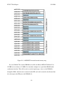
TABLE OF CONTENTS
Abstract
1
1.0 Project Overview and Block Diagram
1
2.0 Team Success Criteria and Fulfillment
2
3.0 Constraint Analysis and Component Selection
2
4.0 Patent Liability Analysis
8
5.0 Reliability and Safety Analysis
11
6.0 Ethical and Environmental Impact Analysis
15
7.0 Packaging Design Considerations
21
8.0 Schematic Design Considerations
28
9.0 PCB Layout Design Considerations
35
10.0 Software Design Considerations
37
11.0 Version 2 Changes
46
12.0 Summary and Conclusions
47
13.0 References
48
Appendix A: Individual Contributions
51
Appendix B: Packaging
57
Appendix C: Schematic
59
Appendix D: PCB Layout Top and Bottom Copper
62
Appendix E: Parts List Spreadsheet
63
Appendix F: Software Listing
66
Appendix G: FMECA Worksheet
102
-ii-
ECE 477 Final Report
Fall 2008
Abstract
The multi-touch remote is a touch based device that will recognize multiple touch
inputs at a time. The user will be able to trace patterns on the screen using multiple fingers at the
same time. The drawn pattern will be displayed on an LCD screen to provide visual feedback to
the user. It will also be interpreted by the microcontroller and tasks performed accordingly. For
example, the speed of the connected motor will be increased if the user drags a thumb and
forefinger away from each other across the surface of the screen. If the user drags the thumb and
forefinger towards each other, this will be interpreted as a command to lower the speed of the
motor. Also, if the device is not used for over 5 minutes, i.e. no touch is detected, then the device
will enter a standby mode. Touching the screen will re-activate the device.
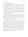
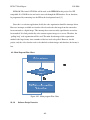
1.0 Project Overview and Block Diagram
The multi-touch remote is motivated by the desire to make the control of home
appliances centralized and more intuitive. The goal is to make multi-touch technology more
mainstream by creating a relatively cheap, user-friendly device that can be used in homes and
make controlling a large range of devices easy.
This revolutionary touch control device will control various home appliances wirelessly.
The device will come with a library of gestures that, when reproduced on the touch screen
surface, will control one of many external electronic devices. This product is able to control any
device that would be found in a typical family room or rec room: lights, television, DVD player,
and stereo.
The overall package dimensions are 15”x12”x10” and the touch screen of the device is
approximately 10”x12” in size. It will be implemented using an acrylic sheet the same size as the
LCD and will be placed on top of the display. The device will use an infrared camera, placed
within the exterior box, to detect touch inputs on the screen. In order to capture images across the
entire screen, the camera will be placed about 8” from the acrylic sheet. The touch inputs will be
replicated on the LCD display in order to give the user visual feedback. A microcontroller will
be used to interpret the pattern drawn by the user. The interpretation of the pattern will be used to
control the speed of a motor connected to the device.
-1-
ECE 477 Final Report
Fall 2008
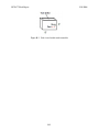
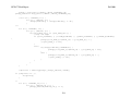
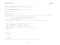
Figure 1-1. Complete Block Diagram
2.0 Team Success Criteria and Fulfillment
1. An ability to detect multiple touch points on the screen using an infrared camera.
2. An ability to capture and display the user drawn touch pattern on the LCD screen.
3. An ability to identify the user drawn touch pattern and to determine whether or not
it is a valid pattern.
4. An ability to go into standby mode if the device has not been used for over 5
minutes.
5. An ability to interpret the user drawn patterns into meaningful output.
3.0 Constraint Analysis and Component Selection
3.1.0
Introduction
Touch Control is a multi-touch device that enables users to easily control home appliances
and entertainment devices by drawing patterns on its surface that will be interpreted as
commands. The device is to be placed on a table or counter top, where it is easily accessible in a
room. Touch Control will be implemented using a camera to capture user input and will have an
-2-
ECE 477 Final Report
Fall 2008
LCD display to give visual feedback to the user. It is important that choices are made to
accommodate for its intended usage scenario and implementation method – it will require a
processor capable of quickly processing the user input and pattern recognition while still able to
handle an LCD display, and its packaging has to be such that it provides a large enough surface
for the user to draw on, but at the same time does not take up too much space on a table. Also,
since it will be left on most of the time, the device should not consume too much power.
3.2.0
Design Constraint Analysis
In order for Touch Control to meet consumer satisfaction, it will have to be aesthetically
pleasing, easy to use, and responsive. The packaging has to give the user enough space to draw
on – preferably at least the size of an average hand spread out, but at the same time be not too tall
such that it is obstructive when placed on a table, and also not have a large footprint as table top
real estate is usually very valuable. This could be a design issue, as the camera has to be placed a
certain distance from the touch surface in order to be able to capture the entire surface.
It should be easy and intuitive for anyone to use – a pattern should not have to be perfectly
replicated in order for the device to recognize it. This would require complex pattern recognition
algorithms in order to account for human error.
It also has to be responsive to the user’s actions – the user should not have to try multiple
times before getting the device to detect his or her touch, and the device should respond quickly
to the user’s input. This involves having good touch-detection and video image processing, as
well as being able to quickly process both touch input and pattern recognition. Note also that an
LCD panel is to be placed in between the touch surface and the camera, and so this has to be
taken into account when considering touch-detection.
Lastly, the device should consume as little power as possible since it will be left on most of
the time. This can be achieved by carefully picking components that do not require lots of power,
and also by having the device enter a low-power standby mode state when appropriate.
2.1 Computation Requirements
First of all, the device has to handle intense video image processing that involves
applying filters to isolate touch inputs, and then figuring out the coordinates of each input. The
device then has to track the location of these inputs and run them against pattern recognition
-3-
ECE 477 Final Report
Fall 2008
algorithms to determine whether or not a valid pattern has been drawn. In addition, the device
needs to be able to keep the LCD display updated by actively having it display a trace of the
user’s touch input. One more major, although relatively less computationally intensive task the
device has to do is to constantly keep track of how long since there has been user input, in order
to enter standby mode when appropriate. Except for the standby mode timer, all of these
computations will have to be done as the user is actively using the device. Once the user touches
the touch surface, the display has to respond immediately, and once a recognizable pattern is
drawn it should be recognized and the appropriate command issued as soon as possible.
2.2 Interface Requirements
Touch Control is a device designed around the idea of creating a new method of intuitive
input and control, and as such has very little inputs and outputs. The only input is the touch
system, and the only output is the LCD display.
2.3 On-Chip Peripheral Requirements
The camera analog output will be fed through an Analog-to-Digital Converter (ADC) and
the ADC’s digital output will received by the main processor. The processor will also have to
output LCD display information. As such, the processor needs to have one interface for sending
digital video data as well as one for receiving similar data. This could be two SPIs. It would also
require two I2C interfaces for controlling the ADC and the LCD controller.
Due to the large memory requirements of image processing, off-chip memory expansion
may be required, in which case the processor should have an external memory controller. Also,
one output compare timer channel will also be needed for the standby mode timer.
Lastly, for the purpose of demonstrating the success of this project, 1 1-bit PWM channel
is required to control the speed of a motor. Alternatively, 1 3-bit PWM channel (or equivalent)
can be used to control the brightness and color of an RGB LED.
2.4 Off-Chip Peripheral Requirements
For the main processor to receive camera data, an ADC is required, preferably one
specialized for video signals. Also, an LCD controller is needed for the processor to control the
LCD display. Lastly, external memory such as SRAM may be required. The size requirement of
-4-
ECE 477 Final Report
Fall 2008
the additional memory is not yet known at the time of this writing as the details of the image
processing algorithms have yet to be finalized.
2.5 Power Constraints
The Touch Control device will be A.C. powered with battery backup. The main purpose
of the battery backup is to ensure that any additional data stored in SRAM is not lost when the
device is disconnected from the A.C. power supply. Heat dissipation should be minimized to
increase overall lifetime of the device, and also to avoid the touch-surface becoming
uncomfortable for the user to touch.
2.6 Packaging Constraints
The footprint of the device should not be larger than the minimum size it has to be, since
it is intended that the device be placed on a table or counter top, where space may be an issue.
This minimum size is dependent on the touch-surface – which needs to have an area large
enough for the user to easily draw patterns on. This area is estimated to be about the size of an
average human hand spread out (roughly 7” x 7”) as this is the maximum size a user may
comfortably draw a pattern.
The device should also not be too tall such that it becomes obstructive when placed on a
table, or is uncomfortable to use in that the touch surface is too high up.
Lastly, the touch-surface should be sturdy enough to withstand any amount of additional
pressure the user may apply, and smooth enough for the user to draw on with his or her bare
fingers.
2.7 Cost Constraints
While the Touch Control is not directly competing with any existing product, it is intended
for home use and thus the cost should be as low as possible in order to be readily available on a
consumer market level. In addition, there are other multi-touch devices such as the iPod Touch
that can be manipulated to gain the same functionality as Touch Control, further reinforcing the
preference to keep costs as low as possible.
3.3.0
Component Selection Rationale
-5-
ECE 477 Final Report
3.1
Fall 2008
Camera
The method of manipulating Frustrated Total Internal Reflection (FTIR) for multi-
touch sensing [1] is being used. This requires a camera that is able to capture IR light, and can be
either a color or monochrome camera. It was found that almost every camera is able to capture
IR light, as long as the IR filter is removed from it, so this is not a huge issue. The camera should
also provide data at a reasonable resolution (at least 320x240 pixels), and in a standard analog
video format. While a camera with a wide-angle lens is preferred to reduce the height of the
device, it produces a distorted image that may be a problem for recognizing the touch input
locations. It has been decided that due to time constraints a regular camera would do, while the
option of the wide-angle lens will be researched on the side. After considering many options,
including CCTVs, it was decided that the CMOS Camera Module (CM-26) from SparkFun was
the best choice due to its reasonable cost, good output resolution, and standard RCA signal
output [2].
3.2
LCD Panel and Controller
The LCD panel needs to be at least as big as the touch surface, in order to display an
indicator where the user touches the surface and to also draw a trace. It does not have to have
excellent quality since only indicators and traces need to be displayed, but should be color for
aesthetic reasons. For cost reasons, we have decided to obtain a cheap computer monitor and
extract the LCD panel and its controller from there. The controller will need to have a standard
video input that can be used to interface with the rest of the device. A good option was found that
meets the above requirements: the Dell 151FP LCD Monitor. Fortunately the university has
donated one to our project. We will need to take it apart and remove the LCD from the
backlight. We will be using an Arduino Atmega168 microcontroller to drive the LCD.
3.3
Microcontroller
In order to cope with the high video image processing computation requirement, the
device should use a DSP chip. The DSP should also specialize in video image processing for
better performance and easier development. The DSPs from Analog Devices were considered
since there is good in-house support provided by the ECE 477 mentors. In particular, their
Blackfin line was considered as it provides sufficient processing power for video and image
-6-
ECE 477 Final Report
Fall 2008
processing [3]. Unfortunately, most of the Blackfin processors came in BGA packaging, which
should be avoided [4]. As such, there were only 2 processors to consider: the ADSP-BF531 and
ADSP-BF532. Both are similar in terms of peripherals and features, except for the amount of onchip SRAM. The BF532 was chosen for having more SRAM (84k vs. 52k) [4] because as much
memory as possible is preferred to allow for more complex image processing and pattern
recognition algorithms.
As a confirmation for this choice, the ADSP-BF532 has a Parallel Peripheral Interface
(PPI) that allows for direct connection to the ADC and in particular can communicate using ITUR 656, a standard digital video format. The DSP also has an external memory controller, and two
general-purpose timers – one for standby mode timer and one for PWM output [5]. The only
peripheral missing is a dedicated I2C interface for controlling the ADC, but this can be
implemented using the spare GPIOs. It is also lacking a second PPI port for video output, but
having an external multiplexer and constantly switching between video input and output can
resolve this.
3.4
Analog-to-Digital Converter
The ADC does not have any specific requirements, other than it accepts the standard
RCA input and outputs using ITU-R 656 encoding. Two ADCs were compared, the first is the
Texas Instruments (TI) TVP5150AM1 and the second the Analog Devices ADV7181, but they
turned out to be almost exactly the same in terms of primary features and requirements. The
Analog Devices ADV7181 was picked because it was the same chip that was on the Blackfin
development kit that we were using.
3.5
LCD Controller
We need a microcontroller that will able to input signals from the main
microcontroller and update the LCD several times a second. We compared the Arduino (which
runs an Atmel Atmega168) and the 9S12C32. Due to time constraints, we had to look at
components that we already had on hand. While the 9S12C32 has a slightly faster clock speed, a
member of our team was more familiar with the Arduino development environment which
allows coding in C. This enables us to speed up implementation, and so the Arduino was
selected.
-7-
ECE 477 Final Report
3.4.0
Fall 2008
Summary
The Touch Control device needs to be responsive to user input. Due to the method used to
capture user input, intense video image processing is required, and for this a DSP chip was
selected as the main controller for the device in order to ensure quick processing. The selected
DSP chip was also able to meet other requirements – namely the ability to receive and send
digital video, have memory expansion capability, and have sufficient general purpose I/O
interfaces. The device also has to hit a sweet spot for its size – enough space to draw on, and at
the same time not take up too much space on a table. To meet this constraint, a suitable camera
for capturing user input and correspondingly a suitably sized LCD panel was selected.
Patent Liability Analysis
4
4.1.0
Introduction
Implementing multitouch surface with infrared camera, and recognize patterns drawn on the
surface. Apple iPhone is the first multi-touch technology used in market that allows users to
control intuitively. And Microsoft Surface is also using multi-touch technology as well. iPhone
filed more than 200 patents for single product, and Microsoft filed pretty large amount also.
Our team is pretty positive that we will have a lot of possible patent infringements in the project.
4.2.0
Results of Patent and Product Search
2.1 Gesture for Touch Sensitive Input Devices (US20080231610) by Apple
Filing Date: 05/09/2008
Abstract: Methods and systems for processing touch inputs are disclosed. The invention in
one respect includes reading data from a multipoint sensing device such as a multipoint touch
screen where the data pertains to touch input with respect to the multipoint sensing device, and
identifying at least one multipoint gesture based on the data from the multipoint sensing device.
Key Claims: A computer implemented method of initiating inertia, the method comprising:
displaying an image on a GUI; detecting a stroke on a touch sensitive surface; noting the speed
and direction of the stroke; moving the image or features embedded in the image in accordance
with the speed and direction of the stroke; and slowing the motion of the image or features
-8-
ECE 477 Final Report
Fall 2008
embedded in the image in accordance with inertia principals when the stroke is no longer
detected.
Possible Infringement/Comment: This is the most recent filed patent founded, filed by
Apple. This patent is not only mentioning how to recognize the motion or pattern, but also
covering entire motion that we can think of. For example, moving fingers outward means
enlarging object on the screen. Most of motion, our project will use in fall in those categories.
The project and iPhone shares same idea of indentifying strokes and holes of the surface, but
Apple is using their own method and we’re planning to use classic method, so I don’t think it
will infringe their patent.
2.2 Physical-virtual interpolation by Microsoft
Filing Date: 02/10/2006
Abstract: A display system and method for use in controlling movement of a virtual image
version of a physical object is described. A physical object may be placed on or near a display
surface, which may sense the presence of the object and display a virtual image version of the
object. In response to movement of the physical object, the virtual image may move as well.
Movement speed of the virtual image may be capped at a maximum speed, so that if the physical
object is moved too quickly, the image will remain moving at a constant maximum speed.
Movement effects, such as blurring, fading, animation, etc. may be applied to the image during
the movement. The movement may change direction as the physical object is detected in
different positions, and the movement effects may be applied to smooth the change in direction
(e.g., curving trajectory).
Key Claim: One or more computer-readable media, storing one or more computerexecutable instructions for performing the following steps: performing a first scanning to detect
the location of a physical object with respect to a display surface; initially displaying, on the
display surface, an image as a virtual representation of said object based on the first scanning;
subsequently performing a second scanning to detect the location of the physical object with
respect to the display surface; identifying a difference in position of the physical object in the
first and second scans; moving the image from a first location towards a second location, the first
and second locations corresponding to positions of the object during said first and second scans,
-9-
ECE 477 Final Report
Fall 2008
respectively; and limiting a speed of motion of the image during the moving step to a maximum
speed.
Possible Infringement/Comment: Patent is referring tracking physical objects and
displaying feedback to user. In our case, physical objects are fingers. If finger moves too fast, it
will be distorted in captured image and won’t be recognized. In this patent, when it lost contact
of an object, it create the virtual path based upon previous data points until it finds actual points
and interpolates. We are not looking that heavy image processing in our microcontroller instead
we will limit users not to move their hands too fast.
2.3 Multi Touch Contact Tracking Algorithm (US 20070081726) by finger works
Filing Date: 14/11/2006
Abstract: Apparatus and methods are disclosed for simultaneously tracking multiple finger
and palm contacts as hands approach, touch, and slide across a proximity-sensing, multi-touch
surface. Identification and classification of intuitive hand configurations and motions enables
unprecedented integration of typing, resting, pointing, scrolling, 3D manipulation, and
handwriting into a versatile, ergonomic computer input device.
Key Claim: A method for associating into paths one or more surface contacts from
successive proximity images, the successive proximity images including a current proximity
image and one or more prior proximity images, the method comprising: generating one or more
predicted paths by predicting from the one or more prior proximity images current positions of
the one or more surface contacts; finding for each surface contact in the current proximity image
a closest predicted path; finding for each predicted path a closest surface contact, the closest
surface contact having a centroid closest to the predicted path; and pairing each surface contact
with its closest predicted path if the surface contact is also the closest surface contact to the
predicted path.
Possible Infringement/Comment: This patent covers exactly what we are trying to do.
Since, we’re getting multiple data points for input, we need to create each plane for each data
point for every frame so that we can find out which finger moved to where. In sense of finding
paths from successive proximity image, we are trying to use the most simple way find centroid
closet to the predicted path, we are exactly infringing their patent.
-10-
ECE 477 Final Report
4.3.0
Fall 2008
Analysis of Patent Liability
Above three patent, except for the one from Microsoft, we have two possible infringement.
First, possible infringement is motion we’re going to use on the surface.
I’m very
knowledgeable in patent law, but I didn’t know that motion on the surface can be even on the
patent. Our project is going to include motions the patent has mentioned, that will be our first
possible infringement. Second, the contact tracking algorithm which is extracting strokes from
consecutive data points. We might not have predicted path, but main algorithm is same. That’s
going to be our second infringement.
4.4.0
Action Recommended
If we are going to put our project on the market, we will have a lot of patent infringement
starting from motion that user going to input, using FTIR method using infrared camera,
algorithm for extracting data points, how to display as well. Core technology such as FTIR, we
can’t avoid to pay loyalty. But other patent, such as extracting path from data points will be
implemented in some other algorithm to reduce the cost of paying loyalty.
4.5.0
Summary
In new technology field such as multitouch, I figured anything can be on the patent. Paying
loyalty for using motion that everybody can think seems like pretty unfair to me. There’s huge
war going on the multitouch patent. Since whichever company gets approved first will dominate
the rest of market, seems like Apple has highest chance to win because of iPhone. Even though
there are thousands of patents in multitouch area, but we’re looking simple touch screens that
will have some limitations to user, we might not confront a lot of infringement, but there are still
some patent that can’t be avoided.
5
Reliability and Safety Analysis
5.1.0
Introduction
The touch control remote is a remote control device for home appliances. It uses camerabased multi-touch sensing to detect patterns drawn by the user on the acrylic touch surface. It is a
box-shaped device that houses the camera and PCB inside it. An LCD is placed beneath the
-11-
ECE 477 Final Report
Fall 2008
acrylic touch surface. Being a home appliance remote control, it is meant to be used in homes. It
can be placed on a table or counter for use. The device is powered by AC power.
The functionality of the device limits any safety issues. The user need never be in prolonged
contact with the device and therefore there is no real safety concern.
The reliability of the device for the most part depends on it’s being able to recognize
patterns correctly.
5.2.0
Reliability Analysis
We chose four components of our design for our failure analysis, the microprocessor, the
SDRAM, the video decoder and the voltage regulator.
2.1 Microprocessor ADSP-BF532
The ADSP-BF532 is a 32 bit microprocessor [2]. Therefore, the following equation
applies for determining its failure rate. The reliability model for microprocessors can be
found in section 5.1 of the military handbook [1].
λP = [C1 πT + C2 πE] πQ πL
Parameter
Value
Description
Comments
C1
0.56
Die Complexity
32 bit microprocessor
C2
0.0555
Package Failure Rate
NP = 134
πT
1.5
Temperature Factor
Max TJ: 1000C
πE
0.5
Environment Factor
Environment GB
πQ
10
Quality Factor
Commercial
πL
1
Learning Factor
> 2 years
λP = 8.6775
MTTF = 13 years.
2.2 SDRAM MT48LC32M16A2
-12-
ECE 477 Final Report
Fall 2008
The SDRAM used in our design is a 16 bit DRAM [3]. Therefore the following equation
can be used to determine its failure rate. This model was obtained from section 5.2 of the
Military Handbook.
λP = [C1 πT + C2 πE] πQ πL
Parameter
Value
Description
Comments
C1
0.0013
Die Complexity
16 bit DRAM
C2
0.0204
Package Failure Rate
NP = 53
πT
2
Temperature Factor
Max TJ: 85 C
πE
0.5
Environment Factor
Environment GB
πQ
10
Quality Factor
Commercial
πL
1
Learning Factor
> 2 years
0
λP = 0.128
MTTF = 892 years.
This is an extremely low failure rate. The SDRAM is therefore not expected to fail during
the device’s lifetime.
2.3 Video Decoder ADV7181
The ADV7181 is a 9 bit video ADC [5]. Its failure rate can be determined by the equation
shown below. This model was obtained from section 5.1 of the Military Handbook.
λP = [C1 πT + C2 πE] πQ πL
Parameter
Value
Description
Comments
C1
0.28
Die Complexity
9 bits
C2
0.0087
Package Failure Rate
NP = 24
πT
0.98
Temperature Factor
Max TJ: 85 C
πE
0.5
Environment Factor
Environment GB
-13-
0
ECE 477 Final Report
Fall 2008
πQ
10
Quality Factor
Commercial
πL
1
Learning Factor
> 2 years
λP = 2.7875
MTTF = 41 years.
2.4 Low Drop Voltage Regulator LD1117
The LD1117 voltage regulators [6] are used in the power supply circuit to generate 3.3V
and 1.8V power inputs. Its failure rate can be determined by the equation shown below.
This model was obtained from section 5.1 of the Military Handbook.
λP = [C1 πT + C2 πE] πQ πL
Parameter
Value
Description
Comments
C1
0.01
Die Complexity
1 to 100 transistors
C2
0.00092
Package Failure Rate
NP = 3
πT
58
Temperature Factor
Max TJ: 125 C
πE
0.5
Environment Factor
Environment GB
πQ
10
Quality Factor
Commercial
πL
1
Learning Factor
> 2 years
0
λP = 5.8046
MTTF = 20 years.
Among the devices analyzed, the microprocessor appears to have the highest failure rate.
This is expected since the microprocessor is the largest device in use on the circuit board
with the maximum number of pins. Hence, it is more likely than the other devices to fail.
5.3.0
Failure Mode, Effects, and Criticality Analysis (FMECA)
The schematic, available in Appendix A, can be split up into the power supply block (A), the
video encoder block (B), the video decoder block (C) and the microcontroller block (D).
-14-
ECE 477 Final Report
Fall 2008
Failures in any of these blocks will lead to loss of device functionality. For the purposes of
this report, failure criticality levels have been defined as follows:
High: Injury to the user.
Medium: Major loss of functionality
Low: Minor loss of functionality
The FEMCA analysis for each of the aforementioned blocks is attached as Appendix B.
5.4.0
Summary
After performing a reliability and safety analysis of the touch control device, it has been
determined that the microcontroller is the component that is most likely to fail. It is followed by
the voltage regulators used in the power supply block.
There are no threats to the user’s safety while using this device. All failure modes only result
in loss of functionality. While some merely cause inconvenience, others are capable of rendering
the device useless.
6
Ethical and Environmental Impact Analysis
6.1.0 Introduction
The goal of our senior design project is to implement a multi touch controller using a CMOS
camera, two microcontrollers, ATD converter and an LCD. For our prototype design we are
using wood to package the design because it is easiest to work with and it will look nice. As we
being to finish up our design, it is important to decide what kind of work we would have to do to
bring this product to market. Before we even think about mass producing and selling this
product we need to take a long hard look at the design and make sure it is ethically sounds and
environmentally safe throughout the products entire life-cycle.
The first step in bringing our product to market would be redesigning our packaging. It
would a be a large challenge to mass produce a product with a wood exterior, even though it has
a good look. The most likely material we could use in the new design would be a hard plastic
mold, because it is very easy to mass produce. A little metal such as aluminum would also be an
option. We would also likely have to make the overall dimensions smaller and use a smaller
LCD. Currently we are using a 15” monitor, because we had one available to us, so we
-15-
ECE 477 Final Report
Fall 2008
constructed the packaging to fit that. The approximate overall dimensions are L = 15.5” x W =
15.5” x H = 10”. We would most likely have to use 10” LCD and make the overall size 2/3 of
our current prototype to bring this product to market.
6.2.0 Ethical Impact Analysis
In order for a product to be ethically sound it must first and foremost be safe. Before we
would be able to bring our design to market we would have to make sure that nothing could go
wrong and cause an injury. The first thing we would have to is make sure all wiring in our
design is completely insulated as well as well connected to appropriate pins. Since our current
packaging material is wood, this is especially important because a loose wire could start a fire.
We also need to be sure that our packaging is completely sealed around the acrylic so that a user
can not get access the electrical components. If we were to sell this product commercially it
would be a good idea to seal it such that if a liquid were to be spilled on the top surface, it would
not get into the components and destroy the device. In order to bring our design to market, we
would also have to stress test the top surface to insure that it will not break and injure someone.
To insure that our product is safe in this area, we could set up different thicknesses of acrylic on
a busted LCD and perform drops tests to see which can withstand enough damage to be safe.
The acrylic material we are using has some flex to it, so I believe that the 3/8” thick sheet we are
using in our current design should withstand a good beating without breaking.
The second most important ethical concern is ensuring that our design would perform
correctly in all operating conditions. This means that our product needs to perform in any
reasonable temperature, humidity and lighting. Our design will not have a problem with the first
two, but getting our design to work in a variety of lighting conditions will be a challenge.
Currently our design needs to be in a darker environment to work correctly. Because the acrylic
sheet and LCD do not block out visible light, a bright environment will allow the camera to pick
up motion outside of the box. This will interfere with the IR lights and will not produce the
correct result. In order to bring this product to market we will need to fix this. Our team has
been looking into IR Optical Filters to solve this problem. We need to test and see if it will work
with our CMOS camera. Another possible solution to this problem would be placing an opaque
piece of acrylic under the LCD. In theory this would block out the visible light, while still
-16-
ECE 477 Final Report
Fall 2008
allowing the IR to go through to the camera. More testing would be need to ensure that this
would work with our design.
6.3.0 Environmental Impact Analysis
In order to understand the environmental impact that our product will have, we will first
break down the products life cycle into four stages; product design, manufacturing/ packaging,
product use, and end of life.
The product design phase is the long and painstaking process we are currently involved in
where we create the initial idea, then create the schematic, PCB, and code. We may not think
about it but we are consuming a lot of power using the lab and personal computers that it takes to
create a project of this scope. This power consumption, no matter how small, will have an
impact on the environment. We are also using raw materials in this phase, to construct the
physical project. We are using a 2 foot by 4 foot piece of ply wood to construct the package for
the prototype, at 12 inch by 14 inch piece of acrylic, a PCB and several electrical components.
Using each one of these materials will have a small environmental impact.
The manufacturing phase will use power consumption and raw material, but exponentially
more than the previous stage. For the sake of mass production, we will be using a hard plastic
mold as the exterior of the device, as opposed to the wood prototype. For this design we will be
using mainly plastic, metal, silicon and acrylic. While using plastic materials is good in the
sense that we do not kill trees to make use them, they are also harmful to the environment to
produce. Many plastic molding machines are responsible for releasing volatile organic
compounds or VOC pollution as well as particulate matter or PM pollution. According to the
Emission Calculation Fact Sheet produced by the Michigan Department of Environmental
Quality, molding machine plastics can produce 1.302E-1 LB PM pollution per ton of plastic and
6.14E-2 LB VOC pollution per ton of plastic. That maybe not seem like a lot, but that definitely
has an effect on the environment. The also take a lot of power to run a molding machine, as well
as to print the PCBs needed to produce lets say a million units. We can reduce our effect on the
environment if we used a more eco-friendly material for the packaging. Probably the best
material to use would be recycled aluminum, but we have to make sure that the metal would not
interfere with or reflect the IR light. Another source of environmental impact is our LCD. Most
of the current LCDs on the market contain nitrogen trifluoride. A recent study has shown that
-17-
ECE 477 Final Report
Fall 2008
this is a harmful greenhouse gas that has negative impact on our climate 10,000 times worse that
carbon dioxide. In order to avoid using products with these harmful chemical, we could use an
OLED display or a green LCD in the manufactured version of our design. The problem with
these display solutions is that they are a little bulkier and much more expensive than the current
‘dirty’ LCDs.
The normal product is one stage where we hope we will have very little environmental
impact. Our product will not produce emissions and it will not use any raw materials, but it will
consume power. The alternative to our product on the market right now would be a standard
TV/VCR remote controller. A regular remote does not consume much power at all so we need
to make our product as efficient as possible. The average remote control, with no display, will
consume approximately 2-5 Watts. Our design, on the other hand, will consume approximately
50-55 Watts during usage. This is a significant difference, but we have a lot more components to
power than the average remote. The main way we are making our design efficient is to have
two power-save modes. The first power save mode will turn off the LCD and the second will
turn off the IR LEDs. The problem is when the device goes into the second power save mode,
the user need to press a push button to wake the device and turn on the IR LEDs. Even though
this is an inconvenience, we thought is was necessary because the LCD and IR LEDs are the
main power draws.
The last stage in the life of our product is the end of life. This occurs when the user has
gotten all the use out of the product and is moving on. Because we are using the mass
production design, with the plastic exterior, our entire design is not biodegradable. The main
solution to this problem is recycling. Unfortunately electronics recycling has not caught on the
way paper and plastic recycling. According to a Goosey and Kellner article, “50,000 tons of
PCB scrap is produced each year in the UK and of this only around 15% is currently subjected to
any form of recycling. The remaining 85% is consigned to landfill.” This a horrible statistic
when you take into account that nearly all PCBs contain traces of lead.
The problem is that the user needs to know how to recycle the product. It is the
manufactures responsibility to inform the consumer about the electrical recycling options out
there. We cannot force the user to recycle; in the end it is completely up to them. Want we can
do is print warnings in the manual as well as on a sticker on the bottom of the device packaging.
I feel that it is important to print a warning directly on the product, in case the user no longer has
-18-
ECE 477 Final Report
Fall 2008
the user manual. The warning must state that this device is not biodegradable and that it must be
recycled because the circuit board contains lead. It must then list a few urls of places to go to
find a location that recycles electronic. There are not a lot of places that do this type of
recycling, but the following websites will be listed on the label:
E-cycle Locator - www.eiae.org/
A Guide to Electronics recycling - http://earth911.com/electronics/
Creative Recycling - http://www.crserecycling.com/
For the amount of electrical scrap that is piling up, there are not enough recycling centers for
printed circuit boards. The main reason for this is that recycling electronics is a long and
expensive process. In order to recover the metals and plastics we want there are several steps.
The device must be striped down as much as possible the sorted, graded and shredded before the
actual recovery process begins. Once the board is shredded, secondary metals, such as iron and
aluminum will be recovered. It is at this time that most of the reusable plastic is recycled and the
unusable scrap is discarded. It is at this time that the smeltering process takes place, whereby the
other metals, such as copper, are recovered. Below there is a flow chart which describes the
recycling process. It is a long and expensive process, but it is a very necessary one for this age
of electronic scrap.
-19-
ECE 477 Final Report
Fall 2008
Figure 1: Flow chart for recycling an electronics assembly, Goosey and Kellner
6.4.0 Summary
In order to bring our product to market we have a lot of work to do! First of all, we would
have to make sure that the design is ethically sound. We must make sure that the device will not
harm anyone and that it performs correctly in all operating conditions. Next we must make sure
that our product is as eco friendly as possible. Our team must ensure that designed and
manufactured using the best materials for our design and the environment. We also have to
design our product to be as power efficient as possible. Lastly, we must urge people to recycle
there electronics and show them why it is bad to just throw away their electronics. In order to
clean up this electronic mess, we all have to pitch in.
-20-
ECE 477 Final Report
Fall 2008
Packaging Design Considerations
7
7.1.0
Introduction
The Touch Control is a remote control utilizing pattern recognition through multi-touch
technology. It is able to interpret patterns drawn by one or more human fingers as commands to
control home appliances and entertainment devices. The Touch Control is a minimalistic singleunit device, having only 1 physical button to toggle power on and off – all other device functions
can be accessed through the top surface which the user draws on. It will be A/C powered, and
can connect to a PC for development or for issuing commands. Ideally, the Touch Control could
be sitting on a tabletop or be carried in one hand of a user, and as such should not be too bulky.
However, due to unavailability of components and for cost reasons, the scope of this project
focuses on implementing multi-touch technology as a means of home automation.
7.2.0
Commercial Product Packaging
The Touch Control is designed to be a remote control for home appliances and
entertainment devices, and ideally should be as small as possible. However, due to the
unavailability of capacitive multi-touch screens, the Touch Control uses the alternative FTIR
implementation of a multi-touch surface. This implementation involves capturing user input via a
camera [1], and as such we will be looking at products with similar multi-touch implementations
– the Microsoft Surface and the NOR_/D Cubit.
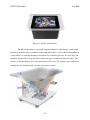
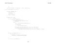
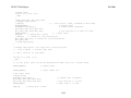
2.1 Product #1 – Microsoft Surface
-21-
ECE 477 Final Report
Fall 2008
Figure 7-1. Picture of the Surface
The Microsoft Surface is a personal computer built into a table that has a multi-touch
interface. It is meant to be a standalone device much like a table – it sits on the floor anywhere in
a room where it is not being obstructive and where it is convenient for users. It is very large and
immobile, but provides a large and sturdy surface for users to touch on and interact with it. The
Surface’s touch and display area is the equivalent of a 30” screen [2], adequate space to allow for
multiple users to simultaneously surround it and interact with it.
-22-
ECE 477 Final Report
Fall 2008
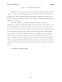
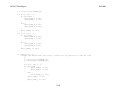
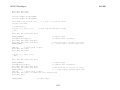
Figure 7-2. Inside the Microsoft Surface
The Surface’s touch surface is made of an acrylic material, and infrared light is directed
towards it from the infrared LED light source place at the bottom of the device. When objects
touch the acrylic surface, the infrared light is reflected back and captured by 4 cameras, each
placed at the 4 corners of the device. For its display, a projector placed at its bottom projects the
display onto the surface [3].
The Touch Control is very much like the Surface in terms of the multi-touch
implementation, with the key differences being that the Touch Control is not meant to be a full
personal computing device, but instead mainly as a home control device, and it typically will
only be used by one user at a time. As such, it does not need to be as large a surface and display,
and does not need to be large enough to house a desktop PC and a projector. Since the Touch
Control’s display is smaller, it needs only one camera for capturing input. Aside from these
differences, the general layout of the Touch Control will be similar to the Surface’s – the top
surface is both the display and the top surface, with the camera placed below it. Making the top
surface the display and touch interface is ideal since it simulates an environment where the user
is drawing (or writing) on a tabletop – a common daily activity that is natural for and familiar to
humans.
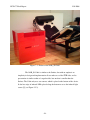
2.2 Product #2 – NOR_/D Cubit
-23-
ECE 477 Final Report
Fall 2008
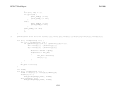
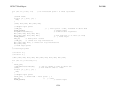
Figure 7-3. Picture of the NOR_/D Cubit
The NOR_/D Cubit is similar to the Surface, but with an emphasis on
simplicity in design and implementation. It too makes use of the FTIR idea, and its
presentation is similar to that of a regular table, but one that is smaller than the
Surface. The Cubit only uses one camera, which is placed at the bottom of the device.
It also has strips of infrared LEDs placed along the bottom to act as the infrared light
source [5] (see Figure 2.2.2).
-24-
ECE 477 Final Report
Fall 2008
Figure 7-4. Diagram Depicting Cubit Construction
The Touch Control uses a LCD panel for its display instead of a projector, in order to
minimize costs. As a side effect, it would not be ideal for the Touch Control’s infrared light
source to be placed at the bottom of the device, as done in the Cubit. This is because each pass
through the LCD panel will reduce the intensity of the infrared light, and by placing the infrared
light source at the bottom it will have to pass through the LCD panel twice before being captured
by the camera. In this case, there is a chance that the final intensity of the infrared light is not
great enough for the camera to capture.
On the other hand, the design of the Cubit is close to the ideal design of the Touch Control,
especially with regards to its simplistic approach. Since the Touch Control will primarily be used
for home automation through touch pattern recognition, it does not need too big of a touch
surface. In addition, it only needs to be big enough for one user at a time.
-25-
ECE 477 Final Report
7.3.0
Fall 2008
Project Packaging Specifications
The Touch Control will resemble a cube, which has 6 surfaces, and the top one of which will
be the touch surface made out of acrylic. Acrylic has been found by many people to be an ideal
material to use for the FTIR method that is being used to implement multi-touch surface. This
theory is further reinforced by the fact that both the Microsoft Surface also uses an acrylic touch
surface [3]. The remaining 5 walls of the cube will be constructed out of acrylic as well, for
aesthetic purposes, but the insides of these surfaces will be painted black. The reason for this will
be covered later in this section. The 6 pieces of acrylic will be fastened together using screws.
The Touch Control will provide a large enough surface for the user to comfortably draw on,
while at the same time not being too large such that it becomes obstructive. Its primary limiting
factor is the size of its display and touch surface.
For its display, the LCD panel from a regular commercial 15” monitor will be used. Since
commercial LCD monitors are high in demand and readily available, they are much cheaper than
specialized standalone LCD panels ($150 versus $250), and by picking this option the cost of the
Touch Control is minimized. In addition, a 15” panel (which leads to a similarly sized touch
surface) is reasonably ideal – not too large such that there will be a lot of unused space, and not
too small that it will be hard for the user to draw on.
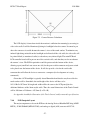
For the touch surface, the FTIR method involves using a camera to capture images from the
touch surface, and as such the camera has to be placed far away enough from the surface in order
to capture the full picture. This distance between the camera and surface is non-trivial, and
depends on the size of the desired area of the touch surface and the camera’s viewing angle. The
FTIR method also requires infrared light to be directed into the touch surface, and to provide this
strips of 4 infrared LEDs will be put on each side of the acrylic touch surface. Both the surface
and the LEDs will be put just above the LCD panel, and as such the available touch area is
slightly smaller than the 15” panel. The LED border will be 5mm thick, leaving a 294.8mm by
218.6mm touch surface area. Given that the viewing angle of the selected camera is [6] and that
the camera will be placed vertically in the center of the touch surface, and also taking into
consideration the area’s longest side, the required distance between the surface and the camera is
(295/2)tan(90-92/2)=142.5mm (see Figure 3.1, below).
-26-
ECE 477 Final Report
Fall 2008
Figure 7-5. Camera Distance Calculation
The LCD display’s frame from inside the monitor is sufficient for mounting by screwing its
sides to the walls. It will be illuminated placing its backlight below the camera. It cannot be put
above the camera as it would obstruct the camera’s view of the touch surface. To minimize any
infrared light being emitted from the backlight and reflected off the side walls, the side walls will
be painted black (as mentioned earlier) to absorb any stray infrared light. The main PCB and
LCD controller board will be put on one of the vertical walls, such that they too do not obstruct
the camera’s view. The PCB in particular would be put towards the bottom of the device,
allowing a port (small hole cut out on one side) for the power cable connector and power switch
to be placed near the bottom of the device. It will also provide a slot for the serial cable
connector that will allow the device to connect to a computer (for development or issuing
commands).
Given that a LCD backlight is typically about 20mm thick and that the acrylic used for the
touch surface will be 5mm thick, the total height of the device will have to be
142.5+20+5=167.5mm. Its length and width will be the same as the LCD panel plus the
additional thickness of the 5mm acrylic walls. Thus, the actual dimensions of the Touch Control
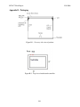
will be 304.8mm x 228.6mm x 167.5mm (L x W x H).
See Appendix A and B for illustration of the Touch Control, and for materials specifications.
7.4.0
PCB Footprint Layout
The major components to be on the PCB are the Analog Devices Blackfin DSP chip (ADSPBF532), 512M SDRAM (MT48LC32M), and analog-to-digital (A/D) converter ADV7181.
-27-
ECE 477 Final Report
Fall 2008
Because the PCB is to be mounted on one side of the device, it can be reasonably large, as long
as it does not obstruct the camera’s view. This gives an allowance for the width of up to about
half the distance between the camera and the touch surface – 142.5/2~=70mm – and for the
height up to about the length of the inside of the device – 294.8/2~=145mm (values rounded
down to allow for buffer space). This is plenty of space, and so the selection of components can
be flexible.
The packaging chosen for the DSP chip was the LQFP primarily because its other option,
BGA, is highly unfavorable for soldering to the PCB. Also, the LQFP packaging is reasonably
small sized at 26mm x 26mm and so is not a major issue [7]. The SDRAM is a typical memory
chip, and since there is no major PCB size restriction, the regular TSOP packaging was selected
[8]. Similar to the DSP, the A/D chip comes in BGA or TQFP packaging [9], and TQFP was
selected since BGA is unfavorable.
For most components, the packaging choice was between one that is easy to solder to a
PCB, and one that is very difficult to do that. Since space is not a huge issue, the obvious choices
were made in favor of the packaging that is easier to solder on.
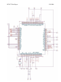
See Appendix C for PCB Footprint Layout illustration.
7.5.0
Summary
The Touch Control is designed for easy pattern drawing by providing the user with a
reasonably sized touch area to draw on, and uses the FTIR multi-touch implementation. The
touch surface will be made of acrylic as it has been proven to be the best available material. A
readily available LCD display size will be used to minimize costs, and the device’s height is just
enough for the camera to capture the whole touch surface area. Due to the spacious interior of the
device, there is no major restriction to the size of the PCB, and the easier to use component
packaging were picked.
8
Schematic Design Considerations
8.1.0 Introduction
For our project, we are designing a gesture based multi touch remote. The Touch
Control will utilize pattern recognition through capacitive touch technology. It is able to
interpret patterns drawn by one or more human fingers as commands to control home
-28-
ECE 477 Final Report
Fall 2008
appliances and entertainment devices. The Touch Control will be a single device, having
only 2 physical buttons to toggle power on and off and reset the device – all other device
functions can be accessed through the top surface which the user draws on.
8.2.0 Theory of Operation
The Touch Control device consists of three main blocks, the main microcontroller, which
will receive camera input, the LCD and the microcontroller that drives it, and the infrared
transmitter/receiver. All of these blocks will be powered by the LCD power supply. We are
going to use two LDOs to drop that voltage from 12V to 3.3 volts and 1.8 volts.
2.1 Input Microcontroller
The main processing component in our multi touch design is the input microcontroller
block, the main component being the Blackfin BF532 microcontroller. The user will be
interacting with the device using the acrylic touch surface. The only other inputs to the
microcontroller are a power switch and a reset button. All the other device functionality will be
achieved by utilizing the touch screen surface. The top acrylic surface will have IR LEDs
pointing directly on the thin edge, on all four sides. This setup will allow the CMOS camera
located several inches below the acrylic to pick up light blobs for every finger that touches the
surface. The microcontroller will take in the digital input from the ADV7181, which converted
the camera input, and use a light threshold to decide when and where the surface has been
touched. Then it will label each touch and trace the motion of the finger. It will create a small
image of what has been traced. The microcontroller will create a separate image for each touch,
therefore giving our design multi touch functionality. If the incoming image data matches a
preloaded gesture, then operation data corresponding to the gestures will be sent out serial to an
output pin that is connected to an infrared LED. For example, if the user draws a horizontal line
on the touch screen, that gesture will be matched in the library to the function, turn on lights.
Then, the operation instruction ‘turn on lights’ will be outputted to the infrared LED. A list of
gestures and there corresponding actions are shown below. More information about the
operation instructions is located in the Infrared Transmission section(2.3).
Lights
-29-
ECE 477 Final Report
Fall 2008
Turn lights on
Turn lights off
Increase brightness
Decrease brightness
Television
Turn TV on
Turn TV off
-30-
ECE 477 Final Report
Fall 2008
Increase volume
Decrease volume
Channel up
Channel down
DVD
Turn DVD on
Turn DVD off
Play
Stop
-31-
ECE 477 Final Report
Fall 2008
Fast-Forward
Rewind
The microcontroller will also output horizontal and vertical coordinates to the LCD
microcontroller serially. When the output to the LCD micro is zero for 30 seconds, the LCD
backlight will be cut off for a power save mode.
2.2 LCD Microcontroller
The LCD micro will constantly read serial data from the main microcontroller. A loop
will sit and wait for these inputs to not equal to zero. While they are both zero, the micro will
cut off power to the LCD, which will serve as a power save mode. When the input on the serial
data is greater than zero, the coordinates will be read in. Then the LCD will be initialized and a
the display loop will be invoked. This loop will draw a green square on the LCD at the proper
coordinates. This will be accomplished in software by writing to the h-sync, v-sync, and green
pins. As the user moves their finger across the touch surface, the coordinates sent to the LCD
micro will be constantly changing and the display loop will be called continuously, so the green
square will follow the user’s finger.
2.3 Infrared Transmission
Along with outputting data to the LCD, the main microcontroller will output a data
instruction to an infrared LED. Whenever the users input matches a gesture in microcontroller’s
‘gesture library’, an 8-bit data instruction will be outputted serially to on an output pin that will
be connected to an IR LED. These instructions will be read by an infrared reciever in another
small circuit across the room. The infrared receiver that we are using is the Panasonic
PNA4601M. This receiver will be connected to a controller which will read the instruction and
control the devices(i.e. lights, TV) accordingly.
-32-
ECE 477 Final Report
Fall 2008
The instruction sent by the microcontroller will be split into two 4-bit codes. The 4 most
significant bits will be the device code. This will control which device is manipulated by the
Touch Control. The 4 least significant bits will be the operation to perform on the external
device. For example, the instruction “0010 0110” will connect with the device with code “0010”
which will be a TV. The operation to perform is the code “0110” which will be decrease the
channel by one. A table of tentative devices and operations is below. Once the operation is
completed the wireless controller will wait for another enable signal.
Device Code
Device
“0001”
Lights
“0010”
TV
“0011”
DVD
“0100”
Stereo
Table 2.1: Devices
Operation Code
Operation
“0001”
Turn Device On
“0010”
Turn Device Off
“0011”
Volume Up/Brighten One Level
“0100”
Volume Down/Dim One Level
“0101”
Channel Up
“0110”
Channel Down
“0111”
Play
“1000”
Stop
“1001”
Fast-Forward
“1010”
Rewind
Table 2.2: Operations
8.3.0 Hardware Design Narrative
The main power supply we are using for this design is the LCD power supply, a 12 volt
source. We are then using 2 LDOs to drop that voltage to 3.3 volts, and then to 1.8 volts. The
-33-
ECE 477 Final Report
Fall 2008
main BF532 micro as well as the LCD micro, oscillator and flash will use 3.3 volts. The decoder
will need both 1.8 volts and 3.3 volts.
The Blacfin BF-532 microcontroller will be using 14 ADDR pins to receive the instruction
address from the flash memory chip. The microcontroller will also input 16 bits of instruction
data from the flash using DATA pins 0-15. The main microcontroller will also receive data from
the ADV7181 video decoder using PPI pins 0-3. Using this input from the video decoder, we
will labeling and hole detection software to trace the image and make sense of it. When a touch
is first seen, the main microcontroller will send two five bit data packets with the touch
coordinates to the LCD micro. The horizontal data bits will be outputted from PF pins 6-10 and
vertical data bits from PF pins 11-15. On the LCD microcontroller, an Ardunio, the horizontal
coordinates will be receive from I/O pins 0-4 and vertical from I/O pins 14-18. The reason for
these pin assignments is so we can read all of pin pad D (pins 0-7) and pin pad C(pins 14-19)
then simply mask off the pins we don’t need. By doing this type of read, we used only a few
clock cycles, so our LCD output timing would not be altered. We originally tried to use a serial
input, but the serial read took over 100 cycles, too long to perform between vertical syncs. Once
the data is received, the LCD micro will then output RGB pins as well as properly timed
horizontal and vertical syncs in order to draw a blob on the LCD where the user has touched.
When the user is done tracing and removes their finger from the touch surface, the software will
then check to see if the gesture match one of the programmed ones. If it does, the main micro
controller will send a serial operation code to the IR transmitter. When the user has not touched
the screen for a few seconds, the LCD encoder will be receiving 0’s for the coordinates. When
this occurs we will cut off the signal to the LCD, causing it to go into power save mode and turn
off the backlight.
We will be using the on chip interrupt system on the BF532 microcontroller in order to call
subroutines to input data from the video decoder. This interrupt will be called very frequently to
make sure that the touch data is continuously updated. The camera interrupt will be running at
60 Hz.
8.4.0 Summary
In order to implement the multi-touch controller, we need to design three main blocks, the
main microcontroller with camera input, the LCD driver, and the IR transmission. The main
-34-
ECE 477 Final Report
Fall 2008
micro needs to receive the touch from the camera, using the chip interrupt system, then send the
appropriate signals to the LCD micro and to the IR transmitter. The LCD micro needs to take
the horizontal and vertical coordinates and draw a blob where the touch occurs. The IR
transmitter will simply take the operation code send by the main microcontroller and send out an
infra red signal containing the operation code.
PCB Layout Design Considerations
9
9.1.0
Introduction
The Mutlitouch Remote requires IR camera, video decoder, DSP, LCD controller, LCD
monitor, SDRAM, voltage regulator and possible use of voltage level shifter. The BlackFin
DSP has ability to acquire video signal or generate RGB signal from its own, so we do not need a
video encoder as originally planned.
9.2.0
PCB Layout Design Considerations – Overall
2.1 CA-84A CMOS Camera [1]
a.
CMOS camera that it generates NTSC signal.
b.
Operating voltage 5V-15V
c.
Current Compsumtion : 12V@150mW
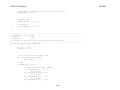
2.2 ADV-7181B Video Decoder [2]
a.
Take NTSC signal through RCA jack.
b.
Output 4:2:2 YCrCb(The process only need grayscale image,
microcontroller will be fed only 4bits Y data.) or I2C interface
c.
3.3V analog, 1.8V digital core, 3.3V IO supply
d.
Analog Interface Inputs: Track lengths should be kept to a minimum, and
75Ω impedances should be used when possible. It is recommended to
decouple each power supply pin with 0.1uF and 10nF capacitors. The
fundamental idea is to have a decoupling capacitor within about 0.5cm of
each power pin. Also, avoid placing the capacitor on the opposite side of
the PC board from the ADV7181B, as doing so interposes resistive vias in
the path. The decoupling capacitors should be located between the power
-35-
ECE 477 Final Report
Fall 2008
plane and the power pin. Current should flow from the power plane to the
capacitor to the power pin. Do not make the power connection between
the capacitor and the power pin.
e.
Digital Outputs : Try to minimize the trace length the digital outputs have to
drive. Longer traces have higher capacitance, which requires more current,
which causes more internal digital noise. Shorter traces reduce the
possibility of reflections. Adding a 30 Ω to 50 Ω series resistor can
suppress reflections, reduce EMI, and reduce the current spikes inside the
ADV7181B. If series resistors are used, place them as close as possible to
the ADV7181B pins. However, try not to add vias or extra length to the
output trace to make the resistors closer.
f.
Digital Inputs : The digital inputs on the ADV7181B are designed to work
with 3.3 V signals, and are not tolerant of 5 V signals. Extra components
are needed if 5 V logic signals are required to be applied to the decoder.
2.3 ADSP-BF532 [3]
-
Details on Section 9.4.0.
2.4 MT48LC32M 512M SDRAM [5]
a.
9.3.0
Voltage Regulators
-
9.4.0
Decoupling capacitors 0.1uF for every power line.
Detail on section 9.5.0
PCB Layout Design Considerations – Microcontroller
-
Powered by 1.2 V (from uC) and 3.3 V (from the voltage regulator)
-
Requires a 40 MHz crystal for a clock signal and a 32.768 KHz crystal for real time
interrupts. According to AN1259, the crystal need to be placed as close as possible.
-
Decoupling capacitors need to be close to the microprocessor as well.
-
Also needs connections to EEPROM, and possible use of FLASH ROM.
-36-
ECE 477 Final Report
9.5.0
Fall 2008
PCB Layout Design Considerations - Power Supply
-
The system needs 3types of input 1.8V, 3.3V and 5.0V. 1.8V and 3.3V are for
microprocessor and video encoder/decoder. 5.0V is for NTSC IR camera. Main
power source is going to be power supply from LCD screen. Assuming the range
of operating voltage is 12V~24V which is suitable input for voltage regulators.
-
Recommend 0.luF for input decoupling capacitor, recommend 10uF for output
decoupling capacitor.
9.6.0
Summary
According to the AN1259, decoupling capacitor needs to be placed as close as the
microprocessor. The PCB need enough trace width for the power line, such as line from voltage
regulators, and power supply.
10 Software Design Considerations
10.1.0
Introduction
The touch control remote is a remote control device for home appliances. The user draws
patterns on the acrylic touch surface. The touch is captured by a camera placed in the box under
the screen. As the user draws the pattern, it is replicated on the LCD screen below the acrylic
touch surface. Once a pattern has been drawn, it is matched against patterns stored in the library
and the corresponding functions are performed by sending out commands using IR. This project
requires a lot of image processing, and hence, the software is a challenging aspect of the design.
The sequence of input images need to be filtered to eliminate noise and large sections of data has
to be manipulated. Also, in order for the device to be an effective remote control device, these
tasks must be performed in real-time.
10.2.0
Software Design Considerations
The microprocessor selected for this project is the ADSP-BF532. This microprocessor
contains high speed serial and parallel ports for interfacing to a variety of audio, video and
modem codec functions. It uses pipelining with three L1 SRAM caches, one for instructions, one
for data and one for scratchpad which houses the stack and local variables. It also has a twelve
channel DMA controller for handling data transfers between external peripherals. The processor
-37-
ECE 477 Final Report
Fall 2008
also offers support for a bank of external SDRAM. Figure 1 shows an internal/external memory
map of the BF532 processor. [1]
Internal SRAM: The internal SRAM has physically separated instruction, data and scratchpad
memory blocks to enable pipelining. These blocks are accessed at full processor speed. The
instruction memory block is 48 kB in size and only holds instructions. It is populated during
bootup from the EEPROM, after which execution begins automatically.
The data memory is 32 kB in size and is configurable, offering both cache and SRAM
functionality.
The scratchpad is 4 kB in size and houses the stack and the local variables.
-38-
ECE 477 Final Report
Fall 2008
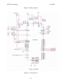
Figure 10-1. ADSP-BF532 internal/external memory map
External SDRAM: The external SDRAM used will be the Micron MT48LC32M16A2. It is
512 MB in size and runs at 133 MHz. It is internally configured as a quad-bank DRAM with a
synchronous interface. This will be used to store the input images. Access to the SDRAM is
through the DMA, which in turn is connected to the PPI, and is able to transfer data directly from
the video input at the PPI port to the SDRAM. [2]
-39-
ECE 477 Final Report
Fall 2008
EEPROM: The Atmel AT25256A will be used as the EEPROM in this project. It is SPI
compatible. It is 256 kB in size and can be accessed through the SPI interface. It can, therefore,
be programmed by connecting it to the SPI on the development board. [3]
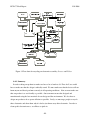
Since this is a real-time application, ideally the code organization should be interrupt driven.
However, interrupts available are from the video decoder after the image from the camera has
been converted to a digital image. This interrupt does not necessarily signal that the screen has
been touched. It is fired periodically as the camera captures images at a set rate. Therefore, the
“polling loop” code organization will be used. The main disadvantage of this organization
method is the large latency since a number of devices need to be polled. However, for this
project, only the video decoder needs to be checked to obtain images and therefore, the latency is
low.
A1: Main Program Flow Chart
Figure 10-2. Main program Flow Chart
10.3.0
Software Design Narrative
-40-
ECE 477 Final Report
Fall 2008
The main program is an infinite loop in which images are obtained from the video decoder.
These images are then filtered to eliminate noise due to visible light, internal reflections, etc.
Each image is also labeled using the labeling algorithm described later and the number of
components/finger-blobs is determined. Coordinates of each blob are determined and used to
separate the original image into different sub-images. As each image is processed, these subimages are built into a separate pattern for each finger. If the image is blank, this means that the
user is currently not touching the screen. This procedure is, therefore, repeated until a non-blank
image is found. At this point the pattern has been built and is now ready to be matched against
the library. The flowchart for can be found below.
A2: Pattern Recognition Subroutine Flowchart
-41-
ECE 477 Final Report
Fall 2008
Figure 10-3. Subroutine Flow Chart
Within the Pattern Recognition subroutine, the pattern is matched against library patterns.
The first blank image indicates that the user’s finger(s) is/are no longer touching the screen. This
implies that the pattern drawing is complete. At this point, the sub-images built for each finger’s
pattern must be examined to determine if it matches a pattern within the library. This is
accomplished by determining the number of patterns and the number of holes in each pattern.
The determined values are compared with the library values and a match is declared.
-42-
ECE 477 Final Report
Fall 2008
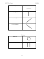
To determine the number of holes, 4 pixel neighborhoods in the pattern image must be
examined. Three ‘0’s and one ‘1’ makes an exterior corner, while three ‘1’s and one ‘0’ makes
an interior corner. The number of holes in the image can be calculated as a quarter of the
difference of the number of exterior and interior corners.
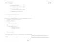
#holes = #interior corner - #exterior corners + number of components
4
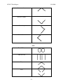
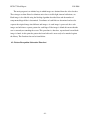
Figure 10-4. Labeling components of a binary image. (a) Original binary image (b) Image after
components labeling (c) Expanded images
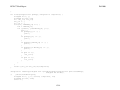
Figure 2 illustrates the labeling of components of the image. To determine the number of
components, the image is processed row-by-row. Two passes are required. During the first pass,
connected components of the image are labeled with the same number. Pixels separated by a 0
are labeled with a different number. During the second pass, equivalent labels are replaced by a
single label. Figure 3 shows the image from figure 2 after each pass. It also illustrates the
resolution of equivalent labels. [4]
-43-
ECE 477 Final Report
Fall 2008
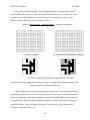
Figure 10-5. Labeling components of a binary image (a) After first pass (b) Equivalent label
resolution (c) After second pass
-44-
ECE 477 Final Report
Fall 2008
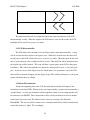
Hierarchical Block Diagram of Code Organization
main()
initPeriph()
filterImage()
patternRecognition()
detectHoles()
detectComponents()
match()
execute(int ID)
Key:
Pre-development
Pseudocode
Written, not tested
Written and tested
Figure 10-6. Code Organization Hierarchy
Relevant code examples available with the evaluation kit can be found here. [5]
-45-
ECE 477 Final Report
10.4.0
Fall 2008
Summary
The Touch Control Remote is a remote controller for home appliances. The software
design for this project relies heavily on image processing and pattern recognition techniques. The
code organization for this device was determined by the non-availability of relevant interrupts.
Hence, the video decoder is polled for input.
The software development for the project is on schedule. Most of the code blocks have
been developed and are in the process of being written. Algorithms are available for code blocks
in the pre-development stage as well from the Computer Vision book.
11 Version 2 Changes
If we were to make a multi-touch controller version 2, we would make some major changes
to its design and packaging as well as add to the controller functionality. The first thing we
would change is the size. Due to the high price of 6” TFT LCDs we decided to use a 15”
computer monitor as our display under the acrylic. This, along with the cameras view angle,
caused our packaging to be quite large, approximately 15” x 13” x 10”. If we were to make a
version 2 and we had more time, money and resources, we could make a design half the size.
We would also look into using a plastic exterior instead of wood, as discussed in the
environment section. If we able to use a 6” LCD, a thin plastic exterior and redesign our PCB to
be a bit smaller, I believe we could achieve a final product with dimensions of approximately 6”
x 5” x 5”, less than half the size of our current design. This would allow the user to use the
controller as a handheld device rather than a table top device.
The second major change would add functionality to the multi-touch controller. Our
current design can only send very simple commands and control only a few devices, mainly
lights and TV. The version 2 design would be able to control more devices and in more ways.
One device we would like to add would be a computer. The device would be able to send
commands to a USB IR receiver that is plugged into a PC and change the volume, change a song
and even scroll through a webpage or document. We could also have the controller interface
with an audio receiver. The controller could change volume song as well as bass and treble
levels and changing the receiver input. In order to implement more devices, we would have to
come up with a lot more gestures so each operation has a unique pattern.
-46-
ECE 477 Final Report
Fall 2008
Lastly, we could change our entire design in order to utilize a new technology. Early
in the design phase, we looked in a capacitive touch screen solution but were unable to obtain the
development kit in time to use in this course. However, if we were to redesign this product and
make a version 2, this would be a viable option. If we were to use capacitive touch technology,
we could make the version 2 device even smaller by reducing the packaging height. Much of the
height of our design is due to the fact that the camera needs space to capture the whole screen. If
we were to use capacitive screen (and 6” LCD, etc.) our overall package size could be as small as
6” x 5” x 2.5”.
12 Summary and Conclusions
In conclusion, we did not achieve the functionality that we had hoped for, but were able to
create a touch screen using acrylic with IR LEDS as a border and a CMOS camera. The device
could not control of the devices but it could label and reproduce the pattern traced on the screen
on the LCD. Our team is disappointed that we could not achieve complete functionality, but we
are still proud of what accomplished in just 4 short months. We took an idea abstract idea and
implemented it in a very unique way. We came up with this unique idea, came up with a design,
created a PCB, wrote hundreds of lines of code, and created a final packaged product in just a
few months. We had to make several design changes at different stages of the implementation
which set us back, but worked thru it.
We learned a lot the semester, probably more than another semester at Purdue. First and
foremost, we learned how much work goes into designing and implementing an embedded
digital system from scratch. So much time went into designing, picking parts, making the
schematic and PCB layout that we didn’t get into lab to start coding and building until halfway
through the semester. We also learned how hard it is to debug an entire system, in particular
debugging the PCB hardware. To debug software you can print values to a terminal or file, but
for hardware you have to get out the DMM and oscilloscope. Even with these devices hooked
up, it is not obvious what is wrong. We burned up several chips at the beginning of the hardware
debugging phase because the LDOs were not outputting the correct voltages. We had to then
wait and work on what we could while we waited for new chips to come.
After months of work and hundreds of hours in the lab we created a touch screen controller.
There are many things that we would change if we could do it over again, or create a version 2,
-47-
ECE 477 Final Report
Fall 2008
but in the end, we worked really hard and got some functionality. Considering to scope and
complexity of our design, to accomplish what we did in 4 months is a great accomplishment.
13 References
[1] J. Han,”FTIR Touch Sensing”, 2005. [Online]. Available:
http://cs.nyu.edu/~jhan/ftirsense/index.html. [Accessed: Sept. 18, 2008].
[2] SparkFun Electronics, “CMOS Camera Module – 640x480”. [Online]. Available:
http://www.sparkfun.com/datasheets/Sensors/Imaging/CM-26N.pdf. [Accessed: Sept. 16,
2008]
[3] Analog Devices, “Embedded Processors and DSP Selection Guide, 2008 Edition”, 2008.
[Online]. Available: http://www.analog.com/static/importedfiles/selection_tables/EP_DSP_Sel_Guide_2008_Web.pdf. [Accessed: Sept. 16, 2008]
[4] Analog Devices, “Blackfin Family Selection Table”, 2008. [Online]. Available:
http://www.analog.com/en/embedded-processing-dsp/blackfin/processors/selectiontables/Blackfin_Selection_Table/resources/fca.html. [Accessed: Sept. 17, 2008]
[5] Analog Devices, “ADSP-BF531/ADSP-BF532/ADSP-BF533 Datasheet”, 2007. [Online].
Available: http://www.analog.com/static/imported-files/data_sheets/ADSPBF531_BF532_BF533.pdf. [Accessed: Sept. 17, 2008]
[6] TI.com, “TVP5150AM1”, 2008. [Online]. Available:
http://focus.ti.com/docs/prod/folders/print/tvp5150am1.html. [Accessed: Sept. 18, 2008]
[7] Analog Devices, “ADV7391”, 2008. [Online]. Available:
http://www.analog.com/en/digital-to-analog-converters/videoencoders/ADV7391/products/product.html. [Accessed: Sept. 18, 2008]
[8] H. Veen, “FTIR multi-touch display how-to guide”, May 23, 2007. [Online]. Available:
http://www.multitouch.nl/documents/multitouchdisplay_howto_070523_v02.pdf.
[Accessed: Oct. 7, 2008]
[9] N. Anderson, “What lurks below Microsoft's Surface? A brief Q&A with Microsoft”, May
30, 2007. [Online]. Available: http://arstechnica.com/news.ars/post/20070530-what-lurksbelow-microsofts-surface-a-qa-with-microsoft.html. [Accessed: Oct. 7, 2008]
[10] G. Derene, “Microsoft Surface: Behind-the-Scenes First Look”, July 2007. [Online].
Available: http://www.popularmechanics.com/technology/industry/4217348.html?page=2.
[Accessed: Oct. 7, 2008]
[11] “CUBIT”, 2008. [Online]. Available: http://nortd.com/cubit. [Accessed: Oct. 7, 2008]
-48-
ECE 477 Final Report
Fall 2008
[12] K. Greene, “Open-Source, Multitouch Display”, May 01, 2008. [Online]. Available:
http://www.technologyreview.com/computing/20703/page1. [Accessed: Oct. 7, 2008]
[13] “CA-84A/C”, 2008. [Online]. Available:
http://www.sparkfun.com/datasheets/Sensors/Imaging/CA-84AC.pdf. [Accessed: Oct. 7,
2008]
[14] Analog Devices, “ADV7181B”, 2008. [Online]. Available:
http://www.analog.com/static/imported-files/data_sheets/ADV7181B.pdf. [Accessed: Oct.
7, 2008]
[15] Analog Devices, “Blackfin Embedded Processor”, 2008. [Online]. Available:
http://www.analog.com/static/imported-files/data_sheets/ADSP-BF531_BF532_BF533.pdf.
[Accessed: Sept. 25, 2008]
[16] Micron, “512Mb: x4, x8, x16 SDRAM Features”, 2008. [Online]. Available:
http://download.micron.com/pdf/datasheets/dram/sdram/512MbSDRAM.pdf. [Accessed:
Oct. 7, 2008]
[17] Analog Devices, “ADV7170/ADV7171”, 2008. [Online]. Available:
http://www.analog.com/static/imported-files/data_sheets/ADV7170_7171.pdf. [Accessed:
Sept. 25, 2008]
[18] “SPI Serial EEPROMs” Atmel,
https://engineering.purdue.edu/477grp4/datasheets/EEPROM.pdf
[19] “Computer Vision” Shapiro, Linda. Stockman, George,
https://engineering.purdue.edu/477grp4/sharepoint/Computer%20Vision%20%20Linda%20Shapiro.pdf
[20] “Military Handbook”, Reliability Prediction of Electronic Equipment, Department of
Defense, 2 January 1990.
[21] “Synchronous DRAM” Micron,
https://engineering.purdue.edu/477grp4/datasheets/SDRAM.pdf
[22] “Digital PAL/NTSC Video Encoder with 10-Bit SSAF and Advanced Power Management”
Analog Devices, https://engineering.purdue.edu/477grp4/datasheets/ADV7171.pdf
[23] “Multiformat SDTV Video Decoder” Analog Devices,
https://engineering.purdue.edu/477grp4/datasheets/ADV7181.pdf
-49-
ECE 477 Final Report
Fall 2008
[24] “LD1117 Series” STMicroelectronics,
https://engineering.purdue.edu/477grp4/datasheets/LDV1117.pdf
[25] Gestures for Touch Sensitive Input Devices, United States Patent Application 20080231610
[26] Physical Virtual Interpolation, United States Patent Application 20080231610
[27] Multi-touch Contact Tracking Algorithm, United States Patent Application 20070081726
[28] Fairchild Semiconductor, “Plastic Infrared Light Emitting Diode”, 2008 [Online].
Available:
http://www.parallax.com/Portals/0/Downloads/docs/prod/audiovis/IRInfoSheet.pdf.
[Accessed October 1, 2008]
[29] Panasonic, “Photo IC”, 2008 [Online]. Available:
http://www.parallax.com/Portals/0/Downloads/docs/prod/audiovis/PNA4601M.pdf.
[Accessed October 1, 2008]
[30] Michigan Department of Environmental Quality, “Emission Calculation Fact Sheet”
[Online document], [Accessed: Nov. 19 2008] Available:
http://www.deq.state.mi.us/documents/deq-ead-caap-maers-EmissionCalculationplasticproducts.pdf
[31] TIA, “E-Cycling Central” [Online document], [Accessed: Nov. 20 2008] Available:
http://www.eiae.org/
[32] Earth 911, “Electronics Recycling” [Online document], [Accessed: Nov. 20 2008]
Available: http://earth911.com/electronics/
[33] Creative Recycling, “Creative Recycling” [Online document], [Accessed: Nov. 20 2008]
Available: http://www.crserecycling.com/
[34] Martin Tarr, “PCB Recycling Issues” [Online document], [Accessed: Nov. 19 2008]
Available: http://www.ami.ac.uk/courses/topics/0113_prei/index.html
-50-
ECE 477 Final Report
Fall 2008
Appendix A: Individual Contributions
A.1 Contributions of Brian Krause:
First of all, I was in charge of the website. At the beginning of the semester I
designed, created and uploaded our team website. I used a free web template that I found online,
then created the different pages, home, about, documents and notebooks. We also have several
links to important web pages like the ece477 homepage and Digikey’s site. I was also in charge
of updating the page are the semester progressed.
My second main objective was to construct the box. This required me to go to the
hardware store get supplies and construct a 15” x 12” x 10” wood box. Then I need to add
brackets for the IR LEDs. I solder the IR LEDs and placed them in these brackets. On the inside
of the box, I needed to attach L brackets to hold up the LCD, add hooks to hold up the LCD’s
circuit board, as well as screwing other components to the side walls. I also had to drill out holes
for the power cord and power and reset buttons.
The next thing that I worked on this semester was the code for the LCD. Our original
design had the Blackfin microcontroller outputting to a video encoder chip (ADV7171) so at first
I wrote code to output from the Blackfin. We later realized that we could not process input and
drive the LCD all one the main micro, so we throw out that code and used a second micro, an
Arduino Atmega168. On the new microcontroller, Dan worked on timing the horizontal and
vertical syncs, and I wrote code to draw a square at a specified coordinate.
I broke up the
nested loops into two loops and turned the video on when the first loop got to the horizontal and
vertical coordinates. This displayed a squared wherever hcoord and vcoord were set to. We
needed the timing to be perfect in order to get a signal and so the box will be straight. This took
a lot of trial and error to get right, so it took a few days. I also wrote and tested code to read the
coordinates from the main micro. We originally were trying to read it in serial, but this took too
long. We were then forced to use extra pins so we can just read the whole port of data in as the
coordinates.
Throughout the semester I was also involved with designing, building and testing the
circuit. I aided Tae in creating and editing the schematic. I also did quite a bit of soldering on
the PCB as well as the connectors. I also did a whole lot of testing. I worked for days just test
A-1
ECE 477 Final Report
Fall 2008
the LCD and getting the timing just right. I also used the oscilloscope to test the PCB’s input
and outputs and figure out what was wrong.
We all had to do two homework papers, but other than that, I was in charge of all the
writing. I wrote the entire user manual, the ECE senior design report, and compiled and edited
all of this final report. I also create the poster for our project. Each of these tasks took a
surprising about of time and effort. It was a rush to get everything completed on time. I worked
around the clock the last week writing papers and testing out the prototype.
A.2 Contributions of Daniel Hum:
My first contribution was to work with Tae and do research on the FTIR multi-touch
implementation. Ranging from the basic idea of it to details such as what type of acrylic to use,
we thoroughly researched the subject to get a good idea of what it is we have to do. We looked at
what other people had done in their attempts to implement a multi-touch interface, and from
there derived our own design. We considered the various possibilities, such as using an actual
LCD panel for display versus using a projected display. For our purposes, the LCD panel was a
much better choice as a projected display would be hard to implement.
I also looked into ways to decrease the size of our project, namely trying to reduce the
distance required between the camera and touch surface. Due to the fixed viewing angle of the
camera, a certain distance is required for the camera to capture the entire touch surface. This
resulted in the height being a limiting factor for our project. I did come up with an idea, which is
to either put a special type of lens (such as a fish-eye lens). However this would result in major
distortion of the captured image, which would require a lot extra algorithms to correct for. To
help alleviate this I also came up with an idea to use a grid array to use as point references, but it
will still require extra software. Unfortunately, either way we came to the decision that it will be
too much extra work that was not required for the purposes of this class.
I also did much of the initial packaging design and components selection. I started
with selecting a camera and appropriate DSP, and from there made suitable selections for the
remaining components, such as the ADC, DAC, and SDRAM. These design decisions were later
reviewed and updated by the rest of the team.
Tae and I were the main two persons working on both the schematic and the PCB
layout. Tae had done most of the initial schematic design, which I later reviewed and made
A-2
ECE 477 Final Report
Fall 2008
modifications or added anything that he had missed. We then worked together to get the PCB
layout done.
I also helped Brian in constructing the box for our project. I worked with him to get
the correct dimensions, and explored various ways of mounting our components (such as the
LCD panel, circuit boards, and camera). I also helped him design and obtain the LED rails.
Lastly, I was in charge of the VGA display module. Due to the last minute discovery
that Tae’s initial idea of directly wiring a NTSC signal to VGA does not work, we had to figure
out an alternative way to get our VGA display working. Unfortunately our DAC does not have a
VGA mode, and after some research our options were to either invest in a VGA module, which
is relatively costly (at least $50) or to create our own using an auxiliary microprocessor. I
decided to go with the latter because I had found good resources for it (one of which
wassoftware for a PIC implementation) and also because getting a new VGA module would also
require time invested to figure out how to communicate with it. I chose to use an Arduino board
that I had on hand, as I was more familiar with its development environment versus the
9S12C32, which I also had. The Arduino development environment allowed development in C,
versus assembly, which sped up initial design and development of the VGA signal routine. While
the 9S12 also as a C development tool, I was not familiar with it.
After a long night of development, I finally came to grasp the entire VGA signal
concept, including the specific timings and syncs it required, and was able to output a proper
VGA signal although just a simple full screen (ie. the video signal is left high the entire time). I
then explained the concept to Brian, who looked through my code and modified it to display only
a box at a specified point. We later refined this technique and added the ability to read in
coordinates through two of the Atema168’s ports. We initially tried reading in through serial, but
the serial read routine took too long and threw off the VGA signal. I then implemented a basic
circuit to test the coordinates system by using DIP switches, and later moved to transferring the
Atmega168 off the Arduino board and onto our own board. I also set up shift registers for the
Blackfin DSP to shift coordinates out onto, so that the VGA module could read from them. This
was needed because the Blackfin had limited GPIO pins.
A-3
ECE 477 Final Report
Fall 2008
A.3 Contributions of Anchal Dube:
At the beginning of the semester, I assumed the responsibility for the software of our project.
During the first few weeks, I helped the team with writing out the project proposal and
determining our PSSCs. The project was Daniel and Tae’s brain child and so I spent most of the
first few weeks educating myself on various aspects of the project, video signals, image
processing, pattern recognition, etc.
I assisted with the PCB development by making footprints for our major chips.
Meanwhile, I also worked on developing an outline for our software. I proposed that we poll the
video decoder continuously to obtain images and first apply a threshold and a noise filter to
them. I further proposed that images of finger-blobs (obtained after the thresholding and
filtering) be superimposed and that a pattern image be built. The idea was to take the pattern built
this way and apply component and holes detection algorithms to it in order to match it against
patterns in the device library.
At the inception of the coding process, I was involved with writing the code that
directly dealt with the pattern recognition. This included the labeling function and also the holes
detection. Later, as the algorithm was modified to split the input image into a single image for
each component, I was responsible for debugging and integrating the code that was written by
Tae. Finally, I also wrote the recognize function which takes the split image patterns and uses the
number of components and number of holes to match against acceptable patterns.
Throughout the software development stage of the project, I have contributed
significantly towards the debugging. I examined the entire software in small chunks and ensured
that all scenarios were accounted for by our software. This was especially tricky for the labeling
function where we attempted to minimize the number of times the image array needed
processing. Several mistakes were made initially, which needed to be correct as and when they
were discovered.
I also assisted Tae with the hardware debugging during the later stages of the project.
Some examples of this are the flash programmer circuit debugging and the SPI – flash interface.
I also worked with Daniel to interface between the two microprocessors being used by our
device.
A-4
ECE 477 Final Report
Fall 2008
Apart from these technical tasks, I was responsible for reliability and safety analysis
report for our team. For this, I researched our chips extensively and analyzed each circuit
component for potential failures.
A.4 Contributions of Tae Kim:
The first thing I achieved is making a prototype using computer. I used acrylic surface
and infrared resistors to implement FTIR multitouch surface. I have to test different
configurations to make it work. But after few changes I had satisfied result using computer.
Polishing each sides of acrylic made a lot of different and making sure that IR is not lighting
other part than inside of acrylic.
My main goal was designing the circuit, the PCB and the whole thing up and running.
I decided most of the components such as microprocessor, video encoder, video decoder, flash,
and SDRAM with Dan. Using video encoder and decoder was more tough than I thought as well
as BlackFin, but it gave me good understanding of how the microprocessor works from the
bottom line. Since we chose not popular microprocessor, we didn¡¯ t have much resource to
refer. I found a lot of resource on line forum, but there are not many people who are actually
making a product with BlackFin but most of them was just dealing with dev board. I worked on
most of the OrCad circuit design as well as PCB layout. It was the first time I was dealing with
the layout and 196pins microprocessor seemed to be little tough, but now I feel confident that I
can use the Layout pretty well.
Next goal was making prototype with dev-board. Initialization was much complicated
than the microprocessor I used. I had to spend a lot of time just to initialize video encoder and
SDRAM. After referring datasheets and example code from the Analog. Especially when using
the SDRAM, making timing correct was main criteria. After all the initialization I was able to
get interrupt every time microprocessor gets the new image. Since, we have to store lots of
images in the SDRAM, I figure to way to allocate the memory in SDRAM, and make sure that is
not trying to allocate the memory in L1 cache. I made the basic structure of the program that it
can be driven by PPI interrupts. Resolution was 720x512, I down sampled to 120x85 just to
make processor to have lower load. Most of the feature we suggested is running under the dev
board now.
A-5
ECE 477 Final Report
Fall 2008
I started to solder chips on the PCB, pitch of microprocessor and video decoder was
very narrow, I had to ask Chuck to help us. Since we are using SPI EEPROM, I need to find
way to write the loader file on to the flash. It would be better if we had JTAG emulator but since
we only had dev board, we decided to use SPI port on the dev board. Making a driver for SPI
flash was pretty tough, actually main reason we chose this flash was the Backseat Driver team
was using this flash, so we thought we would be okay. But on the Blackfin datasheet, it was
recommending different one, so most of other people was using different model. So, I worked
on making the driver for the flash. After writing on to the flash, we had problem that we
couldn¡¯ t boot from the flash, main reason was pullup resistor was required for MISO port and
chip select pin. Then, we could boot with SPI from dev board, but not from our PCB. Main
problem was we chose SPISEL1 to be connected to SPI chip select, but on the datasheet,
SPISEL2 is the only port that can be used for boot procedure. So, pullup resistor and SPISEL2
port changes, I had to make external circuit to hard wire those.
Each of the steps I mentioned took a lot of time. I assumed that it would be pretty
straight forward for board to be run, and actual problem is going to be how we are going to
process the image fast enough for the real-time system. Throughout the semester I spend a lot of
time in the lab trying to figure out stuffs that I assumed easy. I learned a lot from this course
from designing to making a product. And I could take a closer look into the field I¡¯ m very
interested in.
A-6
ECE 477 Final Report
Fall 2008
Appendix B: Packaging
Figure B-1. Cut away side view of product
Figure B-2. Top view of multi-touch controller
B-1
ECE 477 Final Report
Fall 2008
Figure B-3. Side view of multi-touch controller
B-2
ECE 477 Final Report
Fall 2008
Appendix C: Schematic
Figure C-1. Power Supply
C-1
ECE 477 Final Report
Fall 2008
C-2
ECE 477 Final Report
Fall 2008
Figure C-2. Microcontroller
Figure C-3. Video Decoder
C-3
ECE 477 Final Report
Fall 2008
Appendix D: PCB Layout Top and Bottom Copper
Figure D-1. PCB Layout
D-1
ECE 477 Final Report
Fall 2008
Appendix E: Parts List Spreadsheet
Reference Description Manufacturer
Name
Quan. Details
Footprint Link
J3
Female
Serial
Connector Sparkfun
9 Pin Female Serial
Con.
1
U3
Female
VGA
Connector FCI
ICD15S13E6GV00LF
1
D-Sub, High
Density
http://search.digikey.com/scripts/DkSearch/dksus.dll?Detail?name=609-2802-ND
U11
EEPROM
AT25256A
1
SPI Serial 256K 8-SOIC
search digi-key for AT25256A, check In Stock/Lead free/RoHS compliant
J1, J6
Headers
(SPI, Serial) Samtec Inc
TSW-112-08-S-S
1
12POS .100"
SGL GOLD
http://search.digikey.com/scripts/DkSearch/dksus.dll?Detail?name=SAM1046-12-ND
U12
RS-232
Maxim Integrated
Transceiver Products
MAX3222CDWR
1
20-SOIC http://search.digikey.com/scripts/DkSearch/dksus.dll?Detail?name=MAX3222EEWN%2B-ND
U1A
Video A/D
Decoder
Analog Devices
ADV7181BBCPZ
1
64-LFCSP http://search.digikey.com/scripts/DkSearch/dksus.dll?Detail?name=ADV7181BBCPZ-ND
J5
Power
Connector Kobiconn
16PJ031
1
U5
Voltage
Regulator
(3.3V)
U6
SW4
Voltage
Regulator
(1.8V)
Power
Switch
Atmel
http://www.sparkfun.com/commerce/product_info.php?products_id=429
http://www.mouser.com/Search/ProductDetail.aspx?qs=olhD%252bKI%2fybo4iaad1UX7%2fw%3d
STMicroelectronics LDV1117V33
1
IC REG LDO
POS 1.3A 3.3V TO-220
http://search.digikey.com/scripts/DkSearch/dksus.dll?Detail?name=497-1491-5-ND
STMicroelectronics LDV1117V18
1
IC REG LDO
POS 1.3A 1.8V TO-220
http://search.digikey.com/scripts/DkSearch/dksus.dll?Detail?name=497-3457-5-ND
1
E-1
ECE 477 Final Report
Fall 2008
SW3
Reset
Button
U15
MOSFET
Fairchild
Semiconductor
FDS9431A
1
D1
Schottky
Diode
Zetex Inc
ZHCS1000
1
L1
Inductor
(10uH)
Murata Power
Solutions
29103C
1
10uH 1.8A SMD
Shielded
http://search.digikey.com/scripts/DkSearch/dksus.dll?Detail?name=811-1134-1-ND
MC-405
1
32.768kHz
http://search.digikey.com/scripts/DkSearch/dksus.dll?Detail?name=SER2405CT-ND
ADSP-BF532
1
http://search.digikey.com/scripts/DkSearch/dksus.dll?Detail?name=SG-8002CA-PCC-ND
P-Channel 2.5V SO-8
SOT23
U4
Crystal for
Blackfin
Epson Toyocom
Blackfin
DSP
Analog Devices
U13
27Mhz
Oscillator
Epson Toyocom
SG-8002CA-PCC-ND
1
27Mhz Osc
3.3V SMD
U14
Clock
Driver
IDT
IDT74FCT3807AQG
1
1:10 Fanout
Micron
MT48LC32M16A2
1
Ardunio
Atmega168
1
MC 405
U10
EX1
512MB
SDRAM
8 Mhz
Micro
http://search.digikey.com/scripts/DkSearch/dksus.dll?Detail?name=ZHCS1000CT-ND
20-QSOP http://search.digikey.com/scripts/DkSearch/dksus.dll?Detail?name=800-1631-5-ND
54-TSOP http://search.digikey.com/scripts/DkSearch/dksus.dll?Detail?name=557-1078-1-ND
LCD
Microcontroller Off PCB http://www.arduino.cc/en/Hacking/PinMapping168
Resistors
R1
1.69k
R2, R8-14,
R17-19,
R53
10k
1
.1206 SM
12
.1206 SM
R3, R51
100k
2
.1206 SM
R4, R5
5k
2
.1206 SM
R6, R7
100
2
.1206 SM
R50
10M
1
.1206 SM
R52
150
1
.1206 SM
E-2
http://search.digikey.com/scripts/DkSearch/dksus.dll?Detail?name=FDS9431ACT-ND
ECE 477 Final Report
Fall 2008
R54-58
33
5
.1206 SM
R20
110
4
.1206 SM
45
.1206 SM
4
.1206 SM
Capacitors
C7, C1012, C1721, C2427, C3233, C3651, C5456, C5966, C69,
C71, C75 0.1u
C67-68,
C70, C72 0.01u
C30-31
22p
2
.1206 SM
C53-C58
0.1n
2
.1206 SM
C3
82n
1
.1206 SM
C4
10n
100u
(Polarized)
1
.1206 SM
2
Cylinder
10u
(Polarized)
6
Cylinder
Hirose Electric Co FH12-20SConnector Ltd
0.5SH(55)
1
.5mm pitch,
bottom con.
http://search.digikey.com/scripts/DkSearch/dksus.dll?Detail?name=HFJ120CT-ND
Jumper
Cable
1
.5mm pitch, 6"
http://search.digikey.com/scripts/DkSearch/dksus.dll?Detail?name=HFF-20U-06-ND
C22-23
C5, C9,
C34-35,
C73-74
FFC
Extension
Parlex Corp
050R20-152B
E-3
ECE 477 Final Report
Fall 2008
Appendix F: Software Listing
//*********************************************************************************************
//Config.h
has declarations for our main.c file
#define HEAPID
1
#define HEIGHT
#define WIDTH
255
720
#define DS_RATE_X
#define DS_RATE_Y
6
3
#define THRESHOLD
200
#define HEIGHT_DS
#define WIDTH_DS
HEIGHT/DS_RATE_Y
WIDTH/DS_RATE_X
#define BLOBS
5
#define
#define
#define
#define
30
UP_BOUNDARY
DOWN_BOUNDARY 225
LEFT_BOUNDARY 60
RIGHT_BOUNDARY 660
//***********************************************************************************************
//main.c This is the main file that does the input processing. It is in an infinite loop that
//call an input subroutine at a rate of 60 Hz. It then labels the input and detects holes.
//It will then output the coordinates of the touch to the LCD micro.
#include <cdefBF533.h>
#include <stdio.h>
#include <sys\exception.h>
//BF533 Register Pointer Definition
//Interrupt Handling Header
#include <sysreg.h>
#include <ccblkfn.h>
G-1
ECE 477 Final Report
Fall 2008
#include "config.h"
//not needed on PCB
#define pFlashA_PortA_Dir
#define pFlashA_PortA_Out
((volatile unsigned short *)0x20270006)
((volatile unsigned char *)0x20270004)
//not needed on PCB
#define RST_7183 0x8
#define PPICLK_ADV7183_SELECT 0x10
#define ADV7183_OE 0x4
//decoder reset bit #3 in flashA portA
//decoder clock to PPI bit #4 in flashA portA
//ADV7183 /OE = PF2
#define Line_Length 720/2
#define Frame_Length 525
unsigned char bProcessedFlag=0;
unsigned char bInterruptFlag=0;
// addresses for Port B in Flash A --- not needed on PCB
#define pFlashA_PortB_Dir
(volatile unsigned char *)0x20270007
#define pFlashA_PortB_Data
(volatile unsigned char *)0x20270005
#define pFlashA_PortA_Out
((volatile unsigned char *)0x20270004)
void DownSample(void);
void turnonbacklight(void);
void turnoffbacklight(void);
unsigned int labeling(unsigned char *pOriginalImage,unsigned char *pProcessedImage, unsigned int blobs);
unsigned int remove_redundancies(unsigned char *pProcessedImage, unsigned int *redundancies, unsigned int
*count, unsigned int counter, unsigned int blobs);
unsigned int minimum(unsigned int *count, unsigned int counter);
int holes(unsigned char *pImage, unsigned int components);
void clear_images(void);
void draw_blobs(unsigned char *pImageBlob, unsigned int index);
void recognize(void);
//not needed on PCB
// bits for PortB in Flash A conserning LEDs.
#define LED9 0x20
#define LED8 0x10
#define LED7 0x08
G-2
ECE 477 Final Report
Fall 2008
#define LED6 0x04
#define LED5 0x02
#define LED4 0x01
#define COORD_MASK 0x07e0
unsigned
unsigned
unsigned
unsigned
unsigned
unsigned
char * pImage_Blob0;
char * pImage_Blob1;
char * pImage_Blob2;
char * pImage_Blob3;
char * pImage_Blob4;
int prevData[BLOBS][2];
#define NTSC
EX_INTERRUPT_HANDLER(DMA0_PPI_ISR)
// <--|declaration in
{
_pragma(interrupt) the ISR Startaddress
exception.h -->
//
|declaration with
//disable the interrupt request
*pDMA0_IRQ_STATUS = 0x1;
bInterruptFlag = 1;
//*pFIO_FLAG_D ^= PF5;
*pFlashA_PortB_Data ^= LED4;
//printf( "\nThe DMA0 PPI Interrupt has been entered!\n" );
}//end DMA0_PPI_ISR
/*EX_INTERRUPT_HANDLER(Timer0_ISR) {
//confirm interrupt handling
//printf("\nTimer\n");
turnoffbacklight();
*pSIC_IMASK &= ~(0x00010000);
*pTIMER_STATUS = 0x0001;
*pFlashA_PortB_Data ^= LED5;
*pTIMER_DISABLE = 0x0001;
G-3
ECE 477 Final Report
Fall 2008
}*/
void main()
{
int i = 0 ;
//Init PLL
sysreg_write(reg_SYSCFG, 0x32);
//Initialize System Configuration Register
*pSIC_IWR = 0x1;
*pPLL_CTL = 0x2C00;
ssync();
idle();
//Init EBIU
//Setup of the async interface
*pEBIU_AMBCTL0 = 0x7bb07bb0;
ARDY
*pEBIU_AMBCTL1 = 0x7bb07bb0;
4 cycles
*pEBIU_AMGCTL = 0x000F;
// <--|Write access time = 7 cycles, read access time = 11 cycles, no
//
|Hold time = 2 cycles, setup time = 3 cycles, transition time =
//
|Enable all memory banks
//Init Flash
//To use the GPIOs of the flash it must be initialized
*pFlashA_PortA_Out = 0x0;
// clear data registers
*pFlashA_PortA_Dir = 0xFFFF;
// set dir=output
//Init ADV --- not needed on PCB
unsigned char tempReg;
//De-assert the ADV7183 reset and link the ADV7183 Clock "LLC1" to the Blackfin PPI
//clock input.
tempReg = *pFlashA_PortA_Out;
*pFlashA_PortA_Out = tempReg | RST_7183 | PPICLK_ADV7183_SELECT;
//Setup the Blackfin PF registers
G-4
ECE 477 Final Report
Fall 2008
//??????? required? for?
if ( ((*pDSPID) & 0xFFFF) < 0x2 ) {
// Workaround for anomaly ID# 05000079 for rev 0.1
tempReg = *pFIO_INEN;
*pFIO_INEN = tempReg | ADV7183_OE;
}
//Blackfin PF2 pin must be set as output
tempReg = *pFIO_DIR;
*pFIO_DIR = tempReg | ADV7183_OE | COORD_MASK;
//Set the Blackfin pin PF2 to output enable the ADV7183 data bus
tempReg = *pFIO_FLAG_C;
*pFIO_FLAG_C = tempReg | ADV7183_OE;
printf("\n ADV Setup Lock Delay!\n"); //Gives the ADV7183 time to lock after reset
//Init Interrupts
// configure interrupt
*pSIC_IAR0 = *pSIC_IAR0 & 0xffffffff
*pSIC_IAR1 = *pSIC_IAR1 & 0xffffffff
*pSIC_IAR2 = *pSIC_IAR2 & 0xffffffff
//*pSIC_IAR2 = 0xfffffff4; // Timer0
| 0x00000000;
| 0x00000001;
| 0x00000000;
-> ID4;
// map DMA0 PPI Interrupt -> IVG8
register_handler(ik_ivg8, DMA0_PPI_ISR);
vector 8
// assign ISRs to interrupt vectors Timer0 ISR -> IVG 11
//register_handler(ik_ivg11, Timer0_ISR);
// assign DMA0 PPI ISR to interrupt
*pSIC_IMASK=0x00000100; // all interrupts 0=disabled but DMA0 PPI interrupt enabled
// enable Timer0
//*pSIC_IMASK |= 0x00010000;
//Init SDRAM
if (*pEBIU_SDSTAT & SDRS) {
//SDRAM Refresh Rate Control Register
*pEBIU_SDRRC = 0x00000817;
//SDRAM Memory Bank Control Register
*pEBIU_SDBCTL = 0x00000013;
//SDRAM Memory Global Control Register
G-5
ECE 477 Final Report
Fall 2008
*pEBIU_SDGCTL = 0x0091998d;
ssync();
}
//Init DMA
//Target address of the DMA
*pDMA0_START_ADDR = 0x0;
//Line_Length 16bit transfers will be executed
*pDMA0_X_COUNT = Line_Length;
//The modifier is set to 2 because of the 16bit transfers
*pDMA0_X_MODIFY = 0x2;
//Frame_Length 16bit transfers will be executed
*pDMA0_Y_COUNT = Frame_Length;
//The modifier is set to 2 because of the 16bit transfers
*pDMA0_Y_MODIFY = 0x2;
//PPI Peripheral is used
*pDMA0_PERIPHERAL_MAP = 0x0;
//DMA Config: Enable DMA | Memory write DMA | 2-D DMA | Discard DMA FIFO before start | enable
assertation of interrupt | NDSIZE for stop mode | Enable STOP DMA
//*pDMA0_CONFIG = DMAEN | DI_EN | WNR | WDSIZE_16| DMA2D | RESTART | DI_EN;
//*pDMA0_CONFIG = DMAEN | DI_EN | WNR | WDSIZE_16 | RESTART | DMA2D | AUTOBUFFER;
*pDMA0_CONFIG = DMAEN | DI_EN | WNR | WDSIZE_16 | RESTART | DMA2D;
//Init PPI
//The PPI is set to receive 525 lines for each frame
*pPPI_FRAME = 525;
//PPI enabled, input mode, active video only, receive field 1&2,
//packing enabled, skipping disabled, 8bit data bus, nothing inverted
*pPPI_CONTROL = SKIP_EN | PORT_EN | FLD_SEL | PACK_EN | DLEN_8 ;
pImage_Blob0 = heap_malloc(HEAPID,WIDTH_DS*HEIGHT_DS);
G-6
ECE 477 Final Report
pImage_Blob1
pImage_Blob2
pImage_Blob3
pImage_Blob4
Fall 2008
=
=
=
=
heap_malloc(HEAPID,WIDTH_DS*HEIGHT_DS);
heap_malloc(HEAPID,WIDTH_DS*HEIGHT_DS);
heap_malloc(HEAPID,WIDTH_DS*HEIGHT_DS);
heap_malloc(HEAPID,WIDTH_DS*HEIGHT_DS);
clear_images();
while (1)
{
*pFIO_FLAG_D ^= PF6;
if(bInterruptFlag == 1)
{
DownSample();
bInterruptFlag = 0;
}
if(bProcessedFlag == 1)
{
*pPPI_CONTROL = FLD_SEL | PACK_EN | DLEN_8;
*pDMA0_CONFIG = DMAEN | DI_EN | WNR | WDSIZE_16 | RESTART | DMA2D;
*pPPI_CONTROL = SKIP_EN | PORT_EN | FLD_SEL | PACK_EN | DLEN_8 ;
bProcessedFlag = 0;
}
}
}
void DownSample(void)
{
unsigned char * pImage;
unsigned char * oImage;
unsigned char * pImage_Labeled;
unsigned
unsigned int
unsigned
unsigned
unsigned
unsigned
unsigned
int Data[BLOBS][3];
i,j;
int distance;
int components;
int dx,dy,min_dis=99999999;
int min[BLOBS];
int x,y;
oImage = (unsigned char *)0x1;
G-7
ECE 477 Final Report
Fall 2008
pImage = heap_malloc( HEAPID, WIDTH_DS*HEIGHT_DS);
pImage_Labeled = heap_malloc( HEAPID, WIDTH_DS*HEIGHT_DS);
/*for (i=0; i<HEIGHT; i++) {
for (j=0; j<WIDTH; j++) {
oImage[i*WIDTH+j] = oImage[i*WIDTH+j] & 0xF0;
}
}*/
for (i=0; i<HEIGHT; i++) {
for (j=0; j<WIDTH; j++) {
if((i%DS_RATE_Y==0) && (j%DS_RATE_X==0)) {
//chop off edges
if ((i<UP_BOUNDARY) || (i>DOWN_BOUNDARY) || (j<LEFT_BOUNDARY) || (j>RIGHT_BOUNDARY))
{
pImage[(i/DS_RATE_Y)*(WIDTH_DS) + (j/DS_RATE_X)] = 0;
//*pFIO_FLAG_T |= PF5;
}
else {
if(oImage[i*WIDTH+j]>THRESHOLD) {
pImage[(i/DS_RATE_Y)*(WIDTH_DS) + (j/DS_RATE_X)] = 255;
}
else {
pImage[(i/DS_RATE_Y)*(WIDTH_DS) + (j/DS_RATE_X)] = 0;
//*pFIO_FLAG_T |= PF5;
}
}
}
}
}
components = labeling(pImage, pImage_Labeled, BLOBS);
if (components == 0) {
recognize();
}
/*
for (i=0; i<HEIGHT_DS; i++) {
for (j=0; j<WIDTH_DS; j++) {
pImage_Labeled[i*WIDTH_DS+j] *= 10;
G-8
ECE 477 Final Report
Fall 2008
}
}
*/
//printf("\nNumber of Components : %d\n", components);
//////////Storing///////////////
for (i=0; i<BLOBS; i++) {
Data[i][0] = 0;
Data[i][1] = 0;
Data[i][2] = 0;
min[i] = BLOBS;
}
unsigned short temp;
for (i=0; i<HEIGHT_DS; i++) {
for (j=0; j<WIDTH_DS; j++) {
if(pImage_Labeled[i*WIDTH_DS+j]==0)
continue;
else {
temp = pImage_Labeled[i*WIDTH_DS+j];
if(temp>BLOBS)
printf("\nError\n");
Data[pImage_Labeled[i*WIDTH_DS+j]-1][0]+=j; //Storing X
Data[pImage_Labeled[i*WIDTH_DS+j]-1][1]+=i; //Storing Y
Data[pImage_Labeled[i*WIDTH_DS+j]-1][2]++; //Number of Pixels
}
}
}
for (i=0; i<components; i++) {
if (Data[i][2] != 0) {
Data[i][0] = Data[i][0]/Data[i][2];
Data[i][1] = Data[i][1]/Data[i][2];
}
}
x = Data[0][0]*63/WIDTH_DS;
G-9
ECE 477 Final Report
Fall 2008
y = Data[0][1]*63/HEIGHT_DS;
for (i=7; i<8; i--) {
if ((x>>i)&1) {
*pFIO_FLAG_S |= PF6;
*pFIO_FLAG_D |= PF7;
}
else {
*pFIO_FLAG_C |= PF6;
*pFIO_FLAG_D |= PF7;
}
*pFIO_FLAG_D &= ~PF7;
}
for (i=7; i<8; i--) {
if ((y>>i)&1) {
*pFIO_FLAG_S |= PF6;
*pFIO_FLAG_D |= PF7;
}
else {
*pFIO_FLAG_C |= PF6;
*pFIO_FLAG_D|= PF7;
}
*pFIO_FLAG_D &= ~PF7;
}
if (components > 1) {
//maybe some NOPs before this code to ensure that the previous co-ords are read.
/*
x = Data[1][0]*63/WIDTH_DS;
y = Data[1][1]*63/HEIGHT_DS;
for (i=7; i<8; i--) {
if ((x>>i)&1) {
*pFIO_FLAG_S |= PF6;
*pFIO_FLAG_D |= PF7;
}
else {
*pFIO_FLAG_C |= PF6;
*pFIO_FLAG_D |= PF7;
}
*pFIO_FLAG_D &= ~PF7;
G-10
ECE 477 Final Report
Fall 2008
}
for (i=7; i<8; i--) {
if ((y>>i)&1) {
*pFIO_FLAG_S |= PF6;
*pFIO_FLAG_D |= PF7;
}
else {
*pFIO_FLAG_C |= PF6;
*pFIO_FLAG_D|= PF7;
}
*pFIO_FLAG_D &= ~PF7;
}
*/
}
//
printf("\n%u %u %u %u %u %u ",Data[0][0],Data[0][1],Data[1][0],Data[1][1],Data[2][0],Data[2][1]);
for (i=0; i<components; i++) {
for (j=0; j<components; j++) {
if ((prevData[j][0]!=0) || (prevData[j][1]!=0)) {
dx = Data[i][0] - prevData[j][0];
dy = Data[i][1] - prevData[j][1];
distance = dx*dx + dy*dy;
if(distance < min_dis)
{
min_dis = distance;
min[i] = j;
}
}
}
min_dis = 99999999;
}
int index;
for (i=0; i<components; i++) {
index = Data[i][0] + Data[i][1]*WIDTH_DS;
if(min[i] == 0)
draw_blobs(pImage_Blob0, index);
else if(min[i] == 1)
draw_blobs(pImage_Blob1, index);
G-11
ECE 477 Final Report
Fall 2008
else if(min[i] == 2)
draw_blobs(pImage_Blob2, index);
else if(min[i] == 3)
draw_blobs(pImage_Blob3, index);
else if(min[i] == 4)
draw_blobs(pImage_Blob4, index);
prevData[i][0] = Data[i][0];
prevData[i][1] = Data[i][1];
}
/////////////////////////////////
bProcessedFlag = 1;
}
unsigned int minimum(unsigned int *count, unsigned int counter) {
unsigned int min_val, min_index, i;
min_val = count[1];
i = 1;
while (min_val==0) {
i++;
min_val = count[i];
}
min_index = i;
for (i=2; i<=counter; i++) {
if (count[i] != 0) {
if (count[i] < min_val) {
min_val = count[i];
min_index = i;
}
}
}
return min_index;
}
unsigned int remove_redundancies(unsigned char *pProcessedImage,
unsigned int *redundancies, unsigned int
*count,
unsigned int counter, unsigned int blobs) {
unsigned int i, j, k, val;
G-12
ECE 477 Final Report
Fall 2008
redundancies[0] = 0;
count[0] = 0;
val = counter;
k = 1;
for (i=1; i<=counter; i++) {
if (redundancies[i] != 0) {
count[redundancies[i]] += count[i];
count[i] = 0;
val--;
}
}
if (val > blobs) {
for (i=0; i<val-blobs; i++) {
count[minimum(count, counter)] = 0;
}
val = blobs;
}
for (i=1; i<=counter; i++) {
if (count[i] != 0) {
redundancies[i] = k;
k++;
}
else if (redundancies[i] != 0) {
redundancies[i] = redundancies[redundancies[i]];
}
}
for (i=0; i<HEIGHT_DS; i++) {
k=i*WIDTH_DS;
for (j=k; j<k+WIDTH_DS; j++) {
if (redundancies[pProcessedImage[j]] != 0) {
pProcessedImage[j] = redundancies[pProcessedImage[j]];
}
else if (count[pProcessedImage[j]] == 0) {
pProcessedImage[j] = 0;
}
else if (pProcessedImage[j] == 0) {
pProcessedImage[j] = 0;
}
}
}
return val;
G-13
ECE 477 Final Report
Fall 2008
}
int holes(unsigned char *pImage, unsigned int components) {
unsigned int i, j;
unsigned int ref, pix;
int ext_cor, int_cor;
ext_cor = 0;
int_cor = 0;
for (i=1; i<HEIGHT_DS; i++) {
ref = i*WIDTH_DS;
for (j=ref+1; j<ref+WIDTH_DS; j++) {
pix = 0;
if (pImage[j] != 0) {
pix++;
}
if (pImage[j-1] != 0) {
pix++;
}
if (pImage[j-WIDTH_DS] != 0) {
pix++;
}
if (pImage[j-1-WIDTH_DS] != 0) {
pix++;
}
if (pix == 1) {
ext_cor++;
}
if (pix == 3) {
int_cor++;
}
}
}
return ((int_cor-ext_cor)/4)+components;
}
unsigned int labeling(unsigned char *pOriginalImage,unsigned char *pProcessedImage,
unsigned int blobs) {
//
printf("\nLabeling\n");
unsigned int i, j, k, counter, components, val;
unsigned int ref, size;
size = 20;
G-14
ECE 477 Final Report
Fall 2008
unsigned int *redundancies;
unsigned int *count;
redundancies = (unsigned int *) malloc(size*sizeof(unsigned int));
count = (unsigned int *) malloc(size*sizeof(unsigned int));
for (k=0; k<size; k++) {
redundancies[k] = 0;
count[k] = 0;
}
counter = 0;
if (pOriginalImage[0] != 0) {
counter++;
}
pProcessedImage[0] = counter;
count[pProcessedImage[0]]++;
for (j=1; j<WIDTH_DS; j++) {
if (pOriginalImage[j] != 0) {
if (pOriginalImage[j-1] != 0) {
pProcessedImage[j] = pProcessedImage[j-1];
count[pProcessedImage[j]]++;
} else {
counter++;
if (counter >= size) {
size = size*2;
redundancies = (unsigned int *)
realloc(redundancies, size*sizeof(unsigned int));
count = (unsigned int *) realloc(count, size*sizeof(unsigned int));
for (k=size/2; k<size; k++) {
redundancies[k] = 0;
count[k] = 0;
}
}
pProcessedImage[j] = counter;
count[pProcessedImage[j]]++;
}
} else {
pProcessedImage[j] = 0;
}
}
for (i=1; i<HEIGHT_DS; i++) {
ref = i*WIDTH_DS;
if (pOriginalImage[ref] != 0) {
G-15
ECE 477 Final Report
Fall 2008
if (pOriginalImage[ref-WIDTH_DS] != 0) {
pProcessedImage[ref] = pProcessedImage[ref-WIDTH_DS];
count[pProcessedImage[ref]]++;
} else {
counter++;
if (counter >= size) {
size = size*2;
redundancies = (unsigned int *)
realloc(redundancies, size*sizeof(unsigned int));
count = (unsigned int *) realloc(count, size*sizeof(unsigned int));
for (k=size/2; k<size; k++) {
redundancies[k] = 0;
count[k] = 0;
}
}
pProcessedImage[ref] = counter;
count[pProcessedImage[ref]]++;
}
} else {
pProcessedImage[ref] = 0;
}
for (j=ref+1; j<ref+WIDTH_DS; j++) {
if (pOriginalImage[j] != 0) {
if (pOriginalImage[j-WIDTH_DS] != 0) {
pProcessedImage[j] = pProcessedImage[j-WIDTH_DS];
count[pProcessedImage[j]]++;
if (pProcessedImage[j-1] != pProcessedImage[j-WIDTH_DS]) {
val = pProcessedImage[j];
while (val != 0) {
redundancies[pProcessedImage[j-1]] = val;
val = redundancies[val];
}
}
} else if (pOriginalImage[j-1] != 0) {
pProcessedImage[j] = pProcessedImage[j-1];
count[pProcessedImage[j]]++;
} else {
counter++;
if (counter >= size) {
size = size*2;
redundancies = (unsigned int *)
G-16
ECE 477 Final Report
Fall 2008
realloc(redundancies, size*sizeof(unsigned int));
count = (unsigned int *)
realloc(count, size*sizeof(unsigned int));
for (k=size/2; k<size; k++) {
redundancies[k] = 0;
count[k] = 0;
}
}
pProcessedImage[j] = counter;
count[pProcessedImage[j]]++;
}
} else {
pProcessedImage[j] = 0;
}
}
}
components = remove_redundancies(pProcessedImage, &redundancies[0], &count[0],
counter, blobs);
free(redundancies);
free(count);
return components;
}
/*void video_in(void)
{
}
void video_out(void)
{
*pDMA0_START_ADDR = 0x0; // DMA0_START_ADDR
*pDMA0_CONFIG = 0x1090; // DMA0_CONFIG
*pDMA0_X_COUNT = Line_Length; // DMA0_X_COUNT
*pDMA0_X_MODIFY = 0x0001; // DMA0_X_MODIFY
*pDMA0_Y_COUNT = Frame_Length; // DMA0_Y_COUNT
*pDMA0_Y_MODIFY = 0x0001;
*pPPI_CONTROL &= 0x0000;
// PPI Control Register: Output direction, 656 mode.
*pPPI_CONTROL = PORT_DIR; // PPI Port Direction.
G-17
ECE 477 Final Report
Fall 2008
// Unmask DMA interrupt in System Interrupt Controller.
*pSIC_IMASK |= 0x0100;
// Enable DMA
*pDMA0_CONFIG |= 0x0001;
// Enable PPI
*pPPI_CONTROL |= 0x0001;
}*/
//-----------------------------------------------------------------------------// Procedure: Init_ADV7171
// Inputs:
none
// Outputs:
none
// Description: This function initializes the ADV7171 Encoder.
//-----------------------------------------------------------------------------/*void Init_ADV7171(bool NTSC_PAL)
{
bool ret = true;
unsigned int i;
// Init I2C for ADV7171 Indent addr.
if (!I2C_Init(ADV7171_IDENT))
ret = false;
// NTSC
if (NTSC_PAL == true)
{
// Setup ADV7171 Encoder. (NTSC)
if (!I2C_Write(0x00, 0x00))
ret = false;
if (!I2C_Write(0x58, 0x01))
ret = false;
if (!I2C_Write(0x00, 0x02))
ret = false;
if (!I2C_Write(0x00, 0x03))
G-18
ECE 477 Final Report
ret = false;
if (!I2C_Write(0x10,
ret = false;
if (!I2C_Write(0x00,
ret = false;
if (!I2C_Write(0x00,
ret = false;
if (!I2C_Write(0x16,
ret = false;
if (!I2C_Write(0x7C,
ret = false;
if (!I2C_Write(0xF0,
ret = false;
if (!I2C_Write(0x21,
ret = false;
if (!I2C_Write(0x00,
ret = false;
if (!I2C_Write(0x00,
ret = false;
if (!I2C_Write(0x00,
ret = false;
if (!I2C_Write(0x00,
ret = false;
if (!I2C_Write(0x00,
ret = false;
if (!I2C_Write(0x00,
ret = false;
if (!I2C_Write(0x00,
ret = false;
if (!I2C_Write(0x00,
ret = false;
if (!I2C_Write(0x00,
ret = false;
if (!I2C_Write(0x00,
ret = false;
if (!I2C_Write(0x00,
ret = false;
if (!I2C_Write(0x00,
ret = false;
if (!I2C_Write(0x00,
ret = false;
Fall 2008
0x04))
0x07))
0x08))
0x09))
0x0A))
0x0B))
0x0C))
0x0D))
0x0E))
0x0F))
0x10))
0x11))
0x12))
0x13))
0x14))
0x15))
0x16))
0x17))
0x18))
0x19))
G-19
ECE 477 Final Report
Fall 2008
}
// PAL
if (NTSC_PAL == false)
{
// Setup ADV7171 Encoder. (PAL B, D, G, H, I)
if (!I2C_Write(0x05, 0x00))
ret = false;
if (!I2C_Write(0x00, 0x01))
ret = false;
if (!I2C_Write(0x00, 0x02))
ret = false;
if (!I2C_Write(0x00, 0x03))
ret = false;
if (!I2C_Write(0x00, 0x04))
ret = false;
if (!I2C_Write(0x00, 0x07))
ret = false;
if (!I2C_Write(0x00, 0x08))
ret = false;
if (!I2C_Write(0xCB, 0x09))
ret = false;
if (!I2C_Write(0x8A, 0x0A))
ret = false;
if (!I2C_Write(0x09, 0x0B))
ret = false;
if (!I2C_Write(0x2A, 0x0C))
ret = false;
if (!I2C_Write(0x00, 0x0D))
ret = false;
if (!I2C_Write(0x00, 0x0E))
ret = false;
if (!I2C_Write(0x00, 0x0F))
ret = false;
if (!I2C_Write(0x00, 0x10))
ret = false;
if (!I2C_Write(0x00, 0x11))
ret = false;
if (!I2C_Write(0x00, 0x12))
ret = false;
if (!I2C_Write(0x00, 0x13))
G-20
ECE 477 Final Report
ret = false;
if (!I2C_Write(0x00,
ret = false;
if (!I2C_Write(0x00,
ret = false;
if (!I2C_Write(0x00,
ret = false;
if (!I2C_Write(0x00,
ret = false;
if (!I2C_Write(0x00,
ret = false;
if (!I2C_Write(0x00,
ret = false;
Fall 2008
0x14))
0x15))
0x16))
0x17))
0x18))
0x19))
}
// If Error.
if (!ret)
{
while(1)
{
*pFlashA_PortB_Data ^= LED4;
*pFlashA_PortB_Data ^= LED5;
for (i = 0; i < 0x000fffff; i++);
}
}
// Toggle
}*/
//-----------------------------------------------------------------------------// Procedure: I2C_Init
// Inputs:
identaddr
// Outputs:
bool
// Description: Initialize I2C and setup Slave Ident Addr. then check the ident
//
for response and returns true if ok.
//-----------------------------------------------------------------------------/*bool I2C_Init(unsigned char identaddr)
{
bool ret;
// Calculate Delay NEED FIX!!!
G-21
ECE 477 Final Report
Fall 2008
Delay = ((*pPLL_CTL & 0x7e00) >> 9);
Delay = 0x0A;
if ((*pPLL_CTL & 0x0001) == 0x0001)
Delay /= 2;
IdentAddr = identaddr;
Init();
Start();
ret = Write(IdentAddr);
Stop();
// Initialize I2C port
// Check Slave Ident Addr
return ret;
// Return true if Ident Addr. Ok
}*/
//-----------------------------------------------------------------------------// Procedure: I2C_Write
// Inputs:
data out, address
// Outputs:
bool
// Description: Writes a byte to the given address and return status.
//-----------------------------------------------------------------------------/*bool I2C_Write(unsigned char data_out, unsigned char address)
{
Start();
// Send start signal
if (!Write(IdentAddr))
// Send identifier I2C address
{
Stop();
// Send I2C Stop Transfer
return false;
}
if (!Write(address))
// Send address to device
{
Stop();
// Send I2C Stop Transfer
return false;
}
if (!Write(data_out))
// Send byte to device
{
Stop();
// Send I2C Stop Transfer
return false;
}
Stop();
// Send I2C Stop Transfer
G-22
ECE 477 Final Report
Fall 2008
return true;
}*/
//-----------------------------------------------------------------------------// Procedure: I2C_Read
// Inputs:
*data_in, address
// Outputs:
bool
// Description: Reads a byte from the given address and return status.
//-----------------------------------------------------------------------------/*bool I2C_Read(unsigned char *data_in, unsigned char address)
{
Start();
// Send start signal
if (!Write(IdentAddr))
// Send identifer I2C address
{
Stop();
// Send I2C Stop Transfer
return false;
}
if (!Write(address))
// Send address to device
{
Stop();
// Send I2C Stop Transfer
return false;
}
Start();
// Send I2C Start Transer
if (!Write(IdentAddr+1))
// Send identifer I2C address
{
Stop();
// Send I2C Stop Transfer
return false;
}
if (!Read(data_in, false))
// Read byte
{
Stop();
// Send I2C Stop Transfer
return false;
}
Stop();
// Send I2C Stop Transfer
return true;
}*/
//-----------------------------------------------------------------------------// I2C Functions - Master
//------------------------------------------------------------------------------
G-23
ECE 477 Final Report
Fall 2008
//-----------------------------------------------------------------------------//
Routine:
Init
//
Inputs:
none
//
Outputs:
none
//
Purpose:
Initialize I2C for the ADu812C
//-----------------------------------------------------------------------------/*void INL Init(void)
{
*pFIO_DIR
|= SCLK;
// Set SCLK as output and SDATA as input/high
*pFIO_POLAR
&= ~SDATA;
// Enable Active Hight
*pFIO_EDGE
&= ~SDATA;
// Enable Level Sensitivity
*pFIO_INEN
|= SDATA;
// Enable SDATA Input Buffer
SetSDATA(1);
// Set SDATA as input/high
SetSCLK(1);
// Set SCLK high
}
//-----------------------------------------------------------------------------//
Routine:
Start
//
Inputs:
none
//
Outputs:
none
//
Purpose:
Sends I2C Start Trasfer - "S"
//-----------------------------------------------------------------------------void INL Start(void)
{
//
11182003 - Following line has been added! (Fixed thanks to Andrew Seddon).
//
Shouldn't Stop() be setting SCLK high?
SetSCLK(1);
// Set SCLK high
SetSDATA(0);
// Set SDATA output/low
SetSCLK(0);
// Set SCLK low
}
//-----------------------------------------------------------------------------//
Routine:
Stop
//
Inputs:
none
//
Outputs:
none
//
Purpose:
Sends I2C Stop Trasfer - "P"
//-----------------------------------------------------------------------------void INL Stop(void)
{
SetSDATA(0);
// Set SDATA output/low
G-24
ECE 477 Final Report
SetSCLK(1);
SetSDATA(1);
Fall 2008
// Set SCLK high
// Set SDATA as input/high
}
//-----------------------------------------------------------------------------//
Routine:
Write
//
Inputs:
data_out
//
Outputs:
bool
//
Purpose:
Writes data over the I2C bus and return status.
//-----------------------------------------------------------------------------bool INL Write(unsigned char data_out)
{
unsigned char index;
// An I2C output byte is bits 7-0 (MSB to LSB). Shift one bit at a time to
// the SDATA output, and then clock the data to the I2C Slave device.
// Send 8 bits out the port
for (index = 0; index < 8; index++)
{
// Output the data bit to the device
SetSDATA(((data_out & 0x80) ? 1 : 0));
data_out <<= 1;
SetSCLK(1);
SetSCLK(0);
// Shift the byte by one bit
// Set SCLK high
// Set SCLK low
}
SetSDATA(1);
SetSCLK(1);
// Set SDATA input/high
// Set SCLK high
if (!GetSDATA())
{
SetSCLK(0);
return true;
} else
{
SetSCLK(0);
return false;
}
// Set SCLK low
// ACK from slave
// Set SCLK low
// NACK from slave
}*/
G-25
ECE 477 Final Report
Fall 2008
//-----------------------------------------------------------------------------//
Routine:
Read
//
Inputs:
*data_in, send_ack (if true send the ACK signal else send NACK)
//
Outputs:
bool
//
Purpose:
Reads data from the I2C bus and return it in data_in.
//
Returns status.
//-----------------------------------------------------------------------------/*bool INL Read(unsigned char *data_in, bool send_ack)
{
unsigned char index;
*data_in = 0x00;
SetSDATA(1);
SetSCLK(0);
//
//
//
// Set SDATA input/high
// Set SCLK low
// Get 8 bits from the device
for (index = 0; index < 8; index++)
{
*data_in <<= 1;
// Shift the data right 1 bit
SetSCLK(1);
// Set SCLK high
11182003 - Line moved...
SetSCLK(0);
// Set SCLK low
*data_in |= GetSDATA();
// Read the data bit
11182003 - to here! (Fixed thanks to Andrew Seddon).
SetSCLK(0);
// Set SCLK low
}
if (send_ack)
SetSDATA(0);
else
SetSDATA(1);
// Set data pin to output/low to ACK the read
// Set data pin to input/high to NACK the read
SetSCLK(1);
SetSCLK(0);
SetSDATA(0);
SetSDATA(1);
// Set SCLK high
// Set SCLK low
// Set SDATA output/low
// Set SDATA input/high
return true;
}
G-26
ECE 477 Final Report
Fall 2008
//-----------------------------------------------------------------------------//
Routine:
SetSDATA
//
Inputs:
state
//
Outputs:
none
//
Purpose:
Set the I2C port SDATA pin to <state>.
//-----------------------------------------------------------------------------void INL SetSDATA(bool state)
{
unsigned int i, d;
if (state)
{
*pFIO_DIR
&= ~SDATA;
} else
{
*pFIO_DIR
|= SDATA;
*pFIO_FLAG_D &= ~SDATA;
}
// Set SDATA as input/high.
// Set SDATA as output.
// Set SDATA low.
// Delay
for (i = 0; i < Delay; i++) { asm("nop;"); }
}*/
//-----------------------------------------------------------------------------//
Routine:
SetSCLK
//
Inputs:
state
//
Outputs:
none
//
Purpose:
Set the I2C port SCLK pin to <state>.
//-----------------------------------------------------------------------------/*void INL SetSCLK(bool state)
{
unsigned int i, d;
if (state)
{
*pFIO_FLAG_D |= SCLK;
} else
{
*pFIO_FLAG_D &= ~SCLK;
}
// Set SCLK high.
// Set SCLK low.
G-27
ECE 477 Final Report
Fall 2008
// Delay
for (i = 0; i < Delay; i++) { asm("nop;"); }
}
//-----------------------------------------------------------------------------//
Routine:
GetSDATA
//
Inputs:
none
//
Outputs:
bool
//
Purpose:
Get the I2C port SDATA pin state.
//-----------------------------------------------------------------------------bool GetSDATA(void)
{
return ((*pFIO_FLAG_D & SDATA) ? 1 : 0);
}*/
void clear_images(void)
{
int i,j, k;
for (i =0 ;i < HEIGHT_DS ; i++)
{
for ( j = 0 ; j < WIDTH_DS ; j++)
{
k = i*WIDTH_DS+j;
pImage_Blob0[k] = 0;
pImage_Blob1[k] = 0;
pImage_Blob2[k] = 0;
pImage_Blob3[k] = 0;
pImage_Blob4[k] = 0;
}
}
}
void draw_blobs(unsigned char *pImageBlob, unsigned int index)
{
int i, j;
unsigned int x = index % WIDTH_DS;
unsigned int y = index / WIDTH_DS;
if (!(y < 2) && !(y > HEIGHT_DS-1) && !(x < 2) && !(x > WIDTH_DS-1)) {
for (i=y-2; i<y+2; i++) {
for (j=x-2; i<x+2; i++) {
G-28
ECE 477 Final Report
Fall 2008
pImageBlob[i*WIDTH_DS+j] = 255;
}
}
}
}
void recognize(void) {
//done entering pattern
unsigned int i, num_active = 0;
unsigned int temp = 0;
unsigned int holes_array[BLOBS];
for (i=0; i<BLOBS; i++) {
holes_array[i] = 0;
}
temp = labeling(pImage_Blob0, pImage_Blob0, 1);
if (temp)
holes_array[0] = holes(pImage_Blob0, temp);
num_active += temp;
temp = labeling(pImage_Blob1, pImage_Blob1, 1);
if (temp)
holes_array[1] = holes(pImage_Blob1, temp);
num_active += temp;
temp = labeling(pImage_Blob0, pImage_Blob0, 1);
if (temp)
holes_array[0] = holes(pImage_Blob0, temp);
num_active += temp;
temp = labeling(pImage_Blob0, pImage_Blob0, 1);
if (temp)
holes_array[0] = holes(pImage_Blob0, temp);
num_active += temp;
temp = labeling(pImage_Blob0, pImage_Blob0, 1);
if (temp)
holes_array[0] = holes(pImage_Blob0, temp);
num_active += temp;
G-29
ECE 477 Final Report
Fall 2008
//display through LED that num_active blobs are in use
if (num_active == 0) {
return;
}
else if (num_active == 1) {
if (holes_array[0] == 0) {
//one line
}
else if (holes_array[0] == 1) {
//one circle
}
else if (holes_array[0] == 2) {
//8 shaped figure
}
}
else if (num_active == 2) {
if (holes_array[0]+holes_array[1] == 0) {
//two lines
}
else if (holes_array[0]+holes_array[1] == 1) {
//one line and one circle
}
}
clear_images();
}
//********************************************************************************************
//LCD Output code. Inputs data from main micro and displays a green box on the LCD
//where the coordinates are.
#define REDPIN 5
#define HSYNCPIN 7
#define VSYNCPIN 6
// PORTD5
// PORTD7
// PORTD6
#define VIDEO_ON PORTD|=B00100000
#define VIDEO_OFF PORTD&=B11011111
// set portD pin 5 to high
// set back to low
G-30
ECE 477 Final Report
Fall 2008
#define HSYNC_ASSERT PORTD &= B01111111 //set portD pin 7 to low
#define HSYNC_RESET PORTD |= B10000000 //set back to high
#define VSYNC_ASSERT PORTD&=B10111111
#define VSYNC_RESET PORTD|=B01000000
//set portD pin 6 to low
//set back to high
#define COORDS_MASK B00111111
#define NOP asm("nop")
// 1 NOP - 62.5ns
#define ONE_US
asm("nop\n\tnop\n\tnop\n\tnop\n\tnop\n\tnop\n\tnop\n\tnop\n\tnop\n\tnop\n\tnop\n\tnop\n\tnop\n\tnop\n\t")
// 1us / 62.5ns = 16
//14x only, remove one to offset time for next instruction to complete
//
remove one more due to switching time, but will
//
result in slightly less than 1 us (but less than 62.5ns off)
//~.996ns vs 1.06us, slightly less drift
#define TEN_US ONE_US; ONE_US; ONE_US; ONE_US; ONE_US; ONE_US; ONE_US; ONE_US; ONE_US; ONE_US;
void setup()
{
DDRD |= B11100000;
// set hsync, vsync, video pins for output
DDRB &= ~(COORDS_MASK);
// B4,3,2,1,0 xcoords
DDRC &= ~(COORDS_MASK);
// C4,3,2,1,0 ycoords
PORTD &= B11011111;
//initially blank video output
PORTD |= B11000000;
//vsync and hsync assert low. initially de-assert
TIMSK1 = 0x00;
TIMSK2 = 0x00;
cli();
}
void loop()
{
int vcoord = 0;
int hcoord = 0;
asm("VLoop:");
VIDEO_OFF;
for (int i=0; i<10; i++)
{
// 8 lines bottom border + 2 lines vsync front porch
G-31
ECE 477 Final Report
Fall 2008
//blank frame
for(int j=0; j<62; j++) {
NOP;
}
//NOP; NOP; NOP; NOP; NOP; NOP;
//**begin hsync pulse
//ONE_US;
// ; front porch ~.94us, included in above 28us
HSYNC_ASSERT;
// assert hsync
delayMicroseconds(3);
// somehow this is perfect
NOP; NOP; NOP; NOP; NOP; NOP;
NOP; NOP; NOP; NOP; NOP; NOP;
// fix from 3us to ~3.75us (~3.77us)
HSYNC_RESET;
// ; reset hsync
ONE_US;
// back porch ~1.89us
//ONE_US;
// offset for loop instructions
NOP; NOP; NOP; NOP; // offset for loop instructions
NOP; NOP; NOP;
//**end hsync pulse
}
//**begin vsync pulse. note hsync has to still be going
// total 2 hsyncs -> 2 lines occur here
// next 3 lines as in loop above
for(int j=0; j<62; j++) {
NOP;
}
// at this point, about 31.3us has passed since video went low, 10 blank lines.
HSYNC_ASSERT;
// assert hsync
VSYNC_ASSERT;
// vsync assert low
//two vsync lines
//blank frame
delayMicroseconds(3);
NOP; NOP; NOP; NOP; NOP; NOP;
NOP; NOP; NOP; NOP; NOP; NOP;
HSYNC_RESET;
ONE_US;
// somehow this is perfect
// fix from 3us to ~3.75us
// reset hsync ; ~3.77us
// back porch ~1.89us
G-32
ECE 477 Final Report
Fall 2008
NOP; NOP; NOP; NOP;
NOP; NOP; NOP; NOP;
hcoord = PINB & COORDS_MASK;
vcoord = PINC & COORDS_MASK;
if(hcoord > 53) hcoord = 53;
vcoord = vcoord*7;
// 6 ones = 63, max hcoord 53
// previously 50
for(int j=0; j<62; j++) {
// this loop should take 27.32us
NOP;
}
NOP; NOP; NOP; NOP; NOP; NOP;
HSYNC_ASSERT;
delayMicroseconds(3);
NOP; NOP; NOP; NOP; NOP; NOP;
NOP; NOP; NOP; NOP; NOP; NOP;
HSYNC_RESET;
// assert hsync
// somehow this is perfect
// fix from 3us to ~3.75us (~3.77us)
// ; reset hsync, end 1st vsync line
ONE_US;
// back porch ~1.89us
NOP; NOP; NOP; NOP;
NOP; NOP; NOP; NOP;
for(int j=0; j<62; j++) {
NOP;
}
NOP; NOP; NOP; NOP; NOP; NOP;
HSYNC_ASSERT;
// assert hsync
delayMicroseconds(3);
// somehow this is perfect
NOP; NOP; NOP; NOP; NOP; NOP;
NOP; NOP; NOP; NOP; NOP; NOP;
// fix from 3us to ~3.75us (~3.77us)
HSYNC_RESET;
// ; reset hsync, end 2nd vsync line
ONE_US;
// back porch ~1.89us
NOP; NOP; NOP; NOP; // offset for loop instructions
NOP; NOP; NOP;
VSYNC_RESET;
// reset vsync
G-33
ECE 477 Final Report
for (int i=0; i<33; i++)
{
Fall 2008
// 25 lines back porch + 8 lines top border
//blank frame
for(int j=0; j<62; j++) {
NOP;
}
//NOP; NOP; NOP; NOP; NOP; NOP;
//**begin hsync pulse
//ONE_US;
// ; front porch ~.94us, included in above 28us
HSYNC_ASSERT;
// assert hsync
delayMicroseconds(3);
// somehow this is perfect
NOP; NOP; NOP; NOP; NOP; NOP;
NOP; NOP; NOP; NOP; NOP; NOP;
// fix from 3us to ~3.75us (~3.77us)
HSYNC_RESET;
// ; reset hsync
ONE_US;
// back porch ~1.89us
//ONE_US;
// offset for loop instructions
NOP; NOP; NOP; NOP; // offset for loop instructions
NOP; NOP; NOP;
//**end hsync pulse
}
//**end vsync pulse
//vcoord = 300;
//hcoord = 30;
//NOP; NOP; NOP; NOP; NOP; NOP; NOP; NOP; NOP; NOP; NOP; NOP;
for (int i=0; i<vcoord; i++)
{
VIDEO_OFF;
//delayMicroseconds(25);
// ~28 us, seems to take an extra 3us
//NOP;
// fix from 27.94us to ~28us
for(int j=0; j<60; j++) {
NOP;
}
//**begin hsync pulse
VIDEO_OFF; // blank Red - front porch ; 1
ONE_US;
// ; ~.94us
HSYNC_ASSERT;
// assert hsync
G-34
ECE 477 Final Report
Fall 2008
delayMicroseconds(3);
// somehow this is perfect
NOP; NOP; NOP; NOP; NOP; NOP;
NOP; NOP; NOP; NOP; NOP; NOP;
// fix from 3us to ~3.75us
HSYNC_RESET;
// ; ~3.77us
ONE_US;
// back porch ~1.89us
//ONE_US;
// offset for loop instructions
NOP; NOP; NOP; NOP; // offset for loop instructions
NOP; NOP; NOP;
//**end hsync pulse
}
for(int i=0; i<16; i++)
{
VIDEO_OFF;
for(int j=0; j<hcoord; j++)
{
NOP;
}
VIDEO_ON;
NOP; NOP; NOP; NOP; NOP; NOP;
NOP; NOP; NOP; NOP; NOP; NOP;
NOP; NOP; NOP; NOP; NOP; NOP;
NOP; NOP; NOP; NOP; NOP; NOP;
NOP; NOP; NOP; NOP;
// draw square
VIDEO_OFF;
for(int j=hcoord+6; j<60; j++)
{
NOP;
}
//**begin hsync pulse
ONE_US;
// ; ~.94us
HSYNC_ASSERT;
// assert hsync
delayMicroseconds(3);
// somehow this is perfect
NOP; NOP; NOP; NOP; NOP; NOP;
NOP; NOP; NOP; NOP; NOP; NOP;
// fix from 3us to ~3.75us
HSYNC_RESET;
// ; ~3.77us
ONE_US;
// back porch ~1.89us
NOP; NOP; NOP; NOP; // offset for loop instructions
NOP; NOP; NOP; NOP;
G-35
ECE 477 Final Report
Fall 2008
NOP; NOP; NOP; NOP; NOP; NOP;
//**end hsync pulse
}
for (int i=vcoord+10; i<480; i++)
{
VIDEO_OFF;
//delayMicroseconds(25);
// ~28 us, seems to take an extra 3us
//NOP;
// fix from 27.94us to ~28us
for(int j=0; j<60; j++) {
NOP;
}
//**begin hsync pulse
ONE_US;
// ; ~.94us
HSYNC_ASSERT;
// assert hsync
delayMicroseconds(3);
// somehow this is perfect
NOP; NOP; NOP; NOP; NOP; NOP;
NOP; NOP; NOP; NOP; NOP; NOP;
// fix from 3us to ~3.75us
HSYNC_RESET;
// ; ~3.77us
ONE_US;
// back porch ~1.89us
//ONE_US;
// offset for loop instructions
NOP; NOP; NOP; NOP; // offset for loop instructions
NOP; NOP; NOP;
//**end hsync pulse
}
asm("jmp VLoop");
}
G-36
ECE 477 Final Report
Fall 2008
Appendix G: FMECA Worksheet
B1: Power Supply Block (A)
Failure
Failure Mode
No.
A1
Output from
LD1117V33 >
3.3V
Possible Causes
Damaged 3.3V
voltage regulator
Failure Effects
Method of
Detection
Possible failure of Observation
microcontroller,
video encoder,
video decoder.
Criticality
Remarks
Medium
Major loss of
functionality.
A2
Output from
LD1117V18 >
1.8V
Damaged 1.8V
voltage regulator
Possible failure of Observation
video decoder.
Incorrect LCD
display
Low
Minor loss of
functionality.
A3
Outputs less than
3.3V or 1.8V
Damaged voltage
regulator, shorted
bypass capacitors
Unpredictable
Low to
Medium
May lead to failure of
other components or
may not have any
significant effect
G-37
Observation
ECE 477 Final Report
Fall 2008
B2: Video Encoder Block (B)
Failure
Failure Mode
No.
B1
DAC failure
B2
VGA connector
failure
Possible Causes
Failure Effects
Damage to video
DAC chip, improper
initialization
Failure in
processing input
images, resulting
in incorrect LCD
display.
Incorrect output,
resulting in
incorrect LCD
display.
Damaged VGA
connector
G-38
Method of
Detection
Observation
Criticality
Remarks
Low
Minor loss in
functionality
Observation
Low
Minor loss in
functionality
ECE 477 Final Report
Fall 2008
B3: Video Decoder Block (C)
Failure
Failure Mode
No.
C1
ADC failure
Possible Causes
Failure Effects
Damage to video
ADC chip, improper
initialization
Failure in
processing input
images
Method of
Detection
Observation
Criticality
Remarks
Medium
Failure to process input
will result in major loss
of functionality
C2
Camera input
failure
Damaged camera
Corrupt input
from camera.
Observation
Medium
Incorrect input will
result in major loss of
functionality.
C3
RCA jack failure
Damaged RCA jack
Corrupt input
Observation
Medium
Incorrect input will
result in major loss of
functionality.
C4
Noisy output
Damage to video
ADC chip, shorted
filter capacitors
Noisy output
Observation
Low
Pattern recognition will
become harder and may
fail.
G-39
ECE 477 Final Report
Fall 2008
B4: Microcontroller Block (D)
Failure
Failure Mode
No.
D1
Microprocessor
failure
Possible Causes
Failure Effects
Microprocessor
software or hardware
damage.
System may not
work. Possibility
of false data on
output lines
D2
EEPROM failure
or boot failure.
EEPROM failure,
bad boot data
D3
SDRAM failure
or SDRAM
interfacing
failure.
SDRAM failure,
incorrect
initialization.
D4
Clock failure
Damaged crystal.
Method of
Detection
Observation
Medium
Major loss of
functionality
The system will
not boot up
properly, hence
the system may
not run at all or
work incorrectly
The system will
not be access the
external memory
Observation.
Medium
Major loss of
functionality
Internal
software
detection
Low
The microprocessor
will reset itself
The DSP
microprocessor
will run on the
wrong frequency.
Unpredictable.
None
Low to
Medium
The device may or may
not function correctly
G-40
Criticality
Remarks