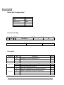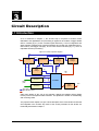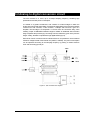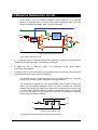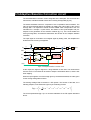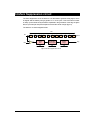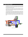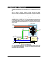
1
CERN – EP/ED $/,&(73&5HDGRXW&KLS 8VHU0DQXDO CERN, June 2002 DRAFT 0.2 INDEX Introduction ____________________________________________________ 5 Chapter 1 ______________________________________________________ 6 1.1 Introduction _____________________________________________________ 6 1.2 Analogue to digital conversion _____________________________________ 8 1.3 Baseline Correction and Subtraction I ______________________________ 10 1.4 Tail Cancellation Filter ___________________________________________ 12 1.5 Baseline Correction and Subtraction II______________________________ 14 1.6 Zero Suppression _______________________________________________ 16 1.7 Data Format ____________________________________________________ 18 1.8 Multi-Event Buffer _______________________________________________ 20 1.9 Trigger Handling ________________________________________________ 21 Chapter 2 _____________________________________________________ 22 2.1 Introduction ____________________________________________________ 22 2.2 ALTRO bus Signals______________________________________________ 23 2.3 Instruction set __________________________________________________ 26 2.4 Registers set ___________________________________________________ 50 2.5 Command Set __________________________________________________ 53 2.6 Control Protocol ________________________________________________ 54 2.7 Modes of Use and Operation ______________________________________ 57 Chapter 3 _____________________________________________________ 58 3.1 Introduction ____________________________________________________ 58 3.2 Analog to digital conversion circuit ________________________________ 59 3.3 Baseline Subtraction circuit ______________________________________ 60 3.4 Tail Cancellation Filter circuit _____________________________________ 62 3.5 Adaptive Baseline Correction circuit _______________________________ 63 3.6 Zero Suppression circuit _________________________________________ 65 3.7 Data Format circuit ______________________________________________ 66 3.8 Multi-Event Buffer circuit _________________________________________ 67 3.9 Hamming State Machines _________________________________________ 1 Introduction 5 Chapter )XQFWLRQDO'HVFULSWLRQ 1.1 Introduction The ALTRO (ALICE TPC Read Out) chip is a mixed analogue-digital custom integrated circuit dedicated to the digitisation and processing of gaseous detector signals. It contains 16 channels operating concurrently on the analogue signals coming from 16 independent inputs. Upon arrival of a first level trigger, each input signal is sampled, processed and stored in a data memory. The maximum number of samples that can be continuously processed for each trigger (data stream) is 1008. When a second level trigger (accept) is received the data stream is either frozen in the data memory, till its complete readout takes place, or discarded. The data memory has the capacity to store 8 data streams. As shown in figure 1.1, after the analogue to digital conversion, the signal processing is performed in 5 steps: a first correction and subtraction of the signal baseline, the cancellation of long-term components of the signal tail, a second baseline correction, the suppression of the samples so close to the baseline that contain no useful information (zero suppression), and formatting. The data processing and the readout of the data memory are performed at different frequencies (different colour in figure 1.1). ACQUISITION CHANNEL (×16) DATA PROCESSOR + 10 ADC – First Baseline Correction Pedestal Memory 11 2'sC 3rd Order Digital Filter 11 2'sC Second Baseline Correction 11 2'sC Zero Supression 11 Multi - Event Buffer 40 Data Format Data Memory 2'sC tw COMMON CONTROL LOGIC Configuration and Status Registers Bus Interface Trigger Manager L1 Runs with Sampling Clock BD CTRL Runs with Readout Clock Figure 1.1. ALTRO Processing Chain 6 L2 Every single ALTRO channel is comprised of 7 main building blocks described hereafter: The analogue input signal is converted into a digital stream by an Analogue-to- Digital Converter (ADC) with 10-bit dynamic range and up to 40 MS/s sampling rate. The first baseline correction corrects the systematic instability of the signal baseline, allowing the subtraction of time-dependant pedestal values taken from the pedestal memory. At this step, the variations of the pedestal in between triggers are also self-corrected. Alternatively the pedestal memory can act as a look-up table, addressed by the input data, that can be used to perform a conversion of the input signal during the pedestal subtraction. Finally the pedestal memory can also be used to generate a test pattern; an important feature that allows a complete test of the overall processing chain without input signal. The signal of a gas detector is often characterised by a long tail with a rather complex shape. An accurate cancellation of the signal tail is required in order to perform efficiently the zero suppression. The tail cancellation filter is based on the approximation of the tail by the sum of exponential functions. Flexibility for the different 16 channels is also given by the possibility to re-configure channel by channel the digital signal processing by changing programmable coefficients. After the tail cancellation a second baseline correction corrects the perturbation of the baseline produced by non-systematic effects. Assuming that systematic and tail-dependant perturbations have been removed in the previous two stages, any remaining deviation is due to non-systematic effects. The second baseline correction computes a moving average on certain samples and then subtracts this value from the signal. The zero suppression is based on a fixed threshold pulse detection scheme, where samples of value smaller than a constant decision level (threshold), are rejected. To reduce the noise sensitivity, a glitch filter checks for a consecutive programmable number of samples above the threshold. In order to keep enough information for further feature extraction, a programmable sequence of pre-samples and post-samples is also recorded. Eventually, the merging of two subsequent sets, closer than 3 samples, is foreseen. The zero suppressed data is formatted in 40 bit words. Every block of samples is labelled with its time and length to allow posterior reconstruction. At the end of the acquisition period, the data block is labelled with a trailer word. The whole structure is back-linked, that is, each trailer word points to the end of the previous data block. Trigger related data is stored in a multiple-event buffer. The Multiple-Event Buffer is a 1024x40 RAM partitioned in a programmable number (4 or 8) of fixed-length buffers. The data is continuously processed, when a trigger is received, a window (Processing Time Window, PTW) defines the stream of data to be formatted and stored in the multievent memory. The implementation of the processing chain requires 18 pipeline stages. With this pipeline a programmable number of samples before the trigger (pre-trigger samples) can be stored by enlarging the PTW. This feature allows the compensation of the trigger latency to the extent of 15 times the sample clock period. The ALTRO chip interfaces to the external world through 16 analogue inputs, a 40 bit bidirectional bus and 8 control signals. The bus protocol is asynchronous for instructions, with a 2-line handshake. The readout, however, is a synchronous block transfer that allows a rate of up to 300 MBytes/s. 7 1.2 Analogue to digital conversion The Analogue to Digital Converter is based on a commercial ADC, the ST Microelectronics TSA1001 [*], slightly modified to suit the ALTRO application. It has a 10-bit dynamic range and up to 25 MHz sampling rate. The ADC has a pipelined architecture, consisting of 9 internal conversion stages, in which the analogue signal is fed and sequentially converted into a digital code. The input analogue signal is sampled on the clock rising edge while the output digital code is issued on the clock’s falling edge. As sketched in figure 1.2, the delay between the initial sample of the input signal and the corresponding output code (data latency) is 5.5 clock cycles. N+4 N+5 N+3 N+6 N+7 N+2 N-1 N+1 N N+8 CL K Tpd + Tod OEB N-7 Ton Toff Tod DAT A OUT N-6 N-5 N-4 N-3 N-2 N+1 N-1 N+2 DR HZ state Figure 1.2. ADC timing diagram. As it will be described in more detail in section 2.1 and 3.1, the ADC is based on a fully differential circuit. It measures the difference (Vd) between the ADC inputs (Vp, positive analogue input and Vn, negative analogue input) while it is insensitive to the absolute values of Vp and Vn, provided within the ALTRO supply voltages. Two reference voltages, Vt (top reference voltage) and Vb (bottom reference voltage), define the dynamic range and the conversion gain accordingly. We introduce, hereafter, some definition and the relationship between the input signal and the digital output code: Reference Range: RR = Vt – Vb Dynamic Range: DR = [-RR ; + RR] Conversion Gain: CG = (2 x DR) / 1024 Digital Output Code = Vd x CG – 512 8 ADC Input V 1.5V 1.5V INCM 0.5V OUT VIN VREFP VINB VREFM VINB VREF 1V 1V OUTB 1.5V PASA VIN 0.5V 0.5V ADC t ADC counts ALICE TPC ADC Output 1023 External Reference: VREFM = 0V; VREFP = INCM = 1V Dynamic Range: (VREFP - VREFM) = 2V 0 t Figure 1.3. A/D converter, signals and configuration. Different configurations for driving the analogue inputs and connecting the reference voltages are discussed in section 2.1. As an example, figure 1.3 shows the configuration that will be used in the ALICE TPC application. 9 1.3 First Baseline Correction The first stage in the digital processing chain is the First Baseline Correction Unit (BC1). The main task of the BC1 is to prepare the signal for the tail cancellation that takes place in the subsequent stage. To this purpose the signal is corrected in order to remove perturbations of different nature. The perturbations affecting the signal from the gas chamber can be: Low-frequency spurious signals (in the range of less than one kilohertz). They perturb the detector signal by shifting its baseline by an amount that, inside the processing time window (PTW), is almost constant (less than one ADC count). This type of signal perturbation could be, for instance, the one produced by a temperature variation of the electronics components. acq #1 acq #2 acq #3 acq #4 acq #5 long-term perturbation Signal perturbations created by systematic effects, like those related to the triggering of the detector, which affect the signal in terms of a superimposed noise pattern. useful signal perturbation To cope with the first effect, a self-calibration circuit is implemented right at the output of the ADC. It tracks continuously the signal outside the PTW computing its cumulative average. Upon the arrival of the first level trigger, the averaging process is interrupted and its last value used as self-calibrated offset to be subtracted to all the samples inside the PTW. To remove systematic effects, a pattern memory is used. Every time the chip starts an acquisition, the values stored in this memory are subtracted from the input signal, thus removing systematic perturbations. Alternatively, this memory can be used as a Look-Up Table (LUT) to perform non-linear conversion or to equalise the response across different channels. As a test feature, this memory can inject a pattern in the processing chain to allow the testing of all the logic downstream without the need of an external analogue signal. 10 The two aforesaid circuits allow for 3 different modes of operation: subtraction mode, conversion mode and test mode. Some of these modes of operation can be combined allowing numerous configurations of the BC1 circuit. The most relevant configurations have been summarised in table 1.1 while the complete list is reported in table 2.x. Hereafter we describe the main modes of operation. Subtraction mode. In this mode of operation, the BC1 performs the subtraction of spurious signals from the input-signal values. The subtracted signal can be fixed (fixed subtraction mode), time-dependent (time-dependent subtraction mode) or self-calibrated (self-calibrated subtraction mode). • In fixed-subtraction mode, the value to be subtracted from the input signal is constant and stored in a configuration register. • In time-dependent subtraction mode, the time-dependent pedestal values to be subtracted are stored in a memory (pedestal memory) that, in this configuration, is addressed by a time counter started by the trigger signal. • In self-calibrated subtraction mode, the value to be subtracted is computed as cumulative average (scp – self calibrated pedestal) of the input signal outside the processing time window: scpn = scpn − 1 + dinn 2 (1) Upon the arrival of the first level trigger, the value of the self-calibrated pedestal is frozen in a register. While the fixed-mode and time-dependent-mode are exclusive, any of them can be combined with the self-calibrated mode as shown in table1.1. Conversion mode. The circuit can perform a memory (static) conversion of the input signal of the type yn = F(xn). At any cycle n, the output yn depends at most on the input sample xn at the same time, but not on past or future samples of the input. The output values yn are stored in the baseline memory addressed, in this case, by the input values xn. The conversion mode can work concurrently to the self-calibrated subtraction mode and to the fixed subtraction mode. Test mode. The LUT can be used to generate a pattern to be injected into the processing chain for test purposes. On this test pattern, which is replacing the input signal samples, can be performed the subtraction of a constant value. In the latter case the pattern generated is a stream of zeros. Finally, the BC1 circuit provide also the possibility of inverting the input signal polarity (1’s complement). The pedestal memory is accessible, in write and read mode, throughout three registers. 0DLQ&RQILJXUDWLRQV 0RGHVRI 2SHUDWLRQ din – fpd din – f(t) din – scp – fpd din – scp – f(t) f(din) – fpd f(din – scp) – fpd f(t) – fpd Fixed Subtraction Time-dependent Mode Self-calibrated 9 9 9 9 9 9 9 9 9 9 9 Conversion Mode 9 9 Test Mode Note: din, data input (samples); f(t), LUT data; fpd, fixed pedestal data value; scp, self-calibrated pedestal data value; f(din), converted data. Table 1.1. ALTRO Baseline Correction and Subtraction I Modes. 11 1.4 Tail Cancellation Filter Although suited for a wider class of applications, the ALTRO chip has been designed for the readout of the cathode pad plane of a conventional multi-wire proportional chamber. In this detector, the necessary signal amplification is provided by an ionisation avalanche created in the vicinity of the anode wires. Moving from the anode wire towards the surrounding electrodes, positive ions, created in the avalanche, induce a positive current signal on the pad plane. This current signal is characterized by a fast rise time (less than 1 ns) and a long tail with a rather complex shape, which depend on the details of the wires and pad geometry. The signal tail increases the superimposition of subsequent pulses (pile-up) rendering the zero suppression quite inefficient. In order to minimize such effect, the ALTRO chip incorporates a filter for the cancellation of the signal tail. The algorithm used for the tail cancellation is explained hereafter. The signal is approximated by the sum of 4 exponential functions: 4 is(t) = I0 × ∑ A i × e − t α⋅τi + r(t) i =1 τ1 << τ 2 << τ3 << τ 4 4 ∑ A i = 1 i=1 (1) Where r(t) is a residual function due to the approximation error. The sum of the gains Ai should be equal to 1 so that input and output have the same amplitude. The time function [1] can be expressed in the Z domain as: 4 Ai + R(z) −1 i =1 1 − exp (T/ τ i ).z Is(z) = I0.∑ (2) The signal is passed through a linear network that cancels all but the fastest of the exponential terms. The n-1 pole-zero network has a transfer function that expressed in the Z domain is: F(z) = (1 − exp (T/ τ 2 ).z −1 )(1 − exp (T/ τ 3 ).z −1 ) (1 − L1z −1 + L 2 z − 2 + L 3 z − 3 ) (3) The numerator of F(z) will perfectly cancel all the poles of Is(z) except one. The constants L1, L2 and L3 are chosen such that the numerator of the expanded form of Is(z) disappears. The response of this linear network to the incoming signal is the convolution in the time of the impulse response function of the filter and the signal itself: is(t) ∗ f(t) = I0 e − t α⋅τ 0 + r(t) ∗ f(t) (4) One can easily observe from this expression that the performance of the tail cancellation is strongly related to r(t). The remaining fast exponential is a constraint of the system and can be chosen such that: − e t α ⋅τ 0 < 0. 1% 12 t ≥ 1 µs (5) The filter considered is an IIR filter of order 3. The filter is composed of 3 first order filters in cascade. The filter is flexible in the configuration of the digital signal processing operation by changing 6 programmable and accessible coefficients, K1, K2, K3, L1, L2 and L3, for each filter. The processing performed is shown in fig 1.4. ADC quantized input signal n exponential aproximation Pole - Zero Transfer function in the Z-Domain H(z) = A B C + + 1 - αz-1 1 - βz-1 1 - γz-1 Output of the Digital Filter F(z) H(z) = Result 1 1 - αz-1 Figure 1.4. Tail Cancellation scheme. The use of the Tail Cancellation Filter in the processing chain can be optional. 13 1.5 Baseline Correction and Subtraction II The second level of baseline correction is apply to the signal during the PTW and corrects signal perturbations created by non-systematic effects, which affect the signal. This level of correction is based on a moving average filter. This functionality is performed in two different levels, one is the generation of the window to perform the average of the baseline (acceptance window), and the other is the correction itself. The correction of the baseline is based on a Moving Average Filter. The acceptance window is based on a double threshold scheme that follows the slow variations of the signal (fig 1.5). Inside the acceptance window, the baseline is corrected subtracting to a given sample the value done by the following equation: y(n) = 1 M ∑ x(n − k ) M + 1 k =0 M=7 (6) This value is the result of the moving average of a signal x(n), in the former case, for a given sample, is the average of this sample and the previous 7. When there is a fast variation in the signal, like a cluster, the samples are out of the acceptance window, and therefore excluded from the baseline calculation. In this case the value of the samples is corrected with the value calculated by the Average Filter for the last sample inside the window. Data excluded from baseline calculation Figure 1.5. . Moving Average Principle. Next figure shows the effect over the baseline of the Adaptive Baseline Correction scheme. 14 Figure 1.6. Data after Adaptive Baseline Correction. The use of pre-sample and post-samples to determine the exclusion window for the baseline calculation is foreseen. 15 1.6 Zero Suppression One obvious way to compress the data stream is to discard “zero” data, e.g., samples so close to the reference level (pedestal) that contain no useful information and can be considered as noise. We are only concerned here with the elimination of the samples with no information - the ones outside the pulses - not with the removal of noise superimposed on the kept samples. The basic pulse detection scheme is fixed thresholding: samples of value smaller than a constant decision level (threshold) are rejected. When a sample is found above the threshold, it is considered the start of a pulse (fig 1.7). THRESHOLD FLAG BIT Figure 1.7. Basic detection scheme. To reduce the impulsive noise sensitivity, a glitch filter checks for a consecutive number of samples above threshold, confirming the existence of a real pulse (fig 1.8). The minimum sequence of samples above the threshold (MINSEQ) which defines a pulse can vary from 1 to 3. MINSEQ = 2 THRESHOLD FLAG BIT Figure 1.8. Glitch filter. In order to keep enough information for further feature extraction, the complete pulse shape must be recorded. Therefore, a sequence of samples (pre-samples) before the signal overcome the threshold and a sequence of samples (post-samples) after the signal returns below the threshold are also recorded (fig 1.9). The number of presamples (PRES) and the number of post-samples (POSTS) can vary independently in the range between 0 and 4. 16 PRES = 2 POSTS = 3 THRESHOLD FLAG BIT Figure 1.9. Feature extraction. The pulse thus identified and isolated must be tagged with a time stamp, in order to be synchronised with the trigger decision for validation. Otherwise the timing information would be lost by the removal of a variable number of samples between accepted pulses. This requires the addition of a time data to the set of sample data. Besides that, in a data format where the addition of flag bits is not allowed, a further word is needed to distinguish the sample data from the time data. This extra word represents the number of words in the set. Since for each new set of data we have two extra words, the merging of two consecutive sets, which are closer than 3 samples, is performed (fig 1.10). PRES = 2 POSTS = 0 THRD FLAG BIT Figure 1.10. Merging of close clusters. 17 1.7 Data Format The stream of zero-suppressed data must be formatted by adding, to each set of samples, two extra words, and encoding the 10-bit words and hardware address into a 40-bit set of words. As it was mentioned in the previous paragraph, due to the removal of a variable number of samples between accepted clusters, the timing information would be lost during the zero-suppression process. This requires the addition of a time data to each accepted set of samples. Since 1000 is the maximum length of the data stream that can be processed by the ALTRO chip, the time information can be encoded in a 10-bit word. The principle is to label each sample with a time-stamp that defines the time distance from the trigger signal. So the samples of the processed data stream are numbered starting from 0 to 1000. The time information added to each cluster during the formatting phase corresponds to the time-stamp of the last sample in the cluster. The ALTRO data format does not make use of extra flag bits to distinguish the samples data from the time data, but introduces a further word for each accepted cluster, which represents the number of words in the cluster without counting the time data. These new 10-bit words, time data and number of samples per cluster, are introduced at the end of the cluster (fig 1.11). ADC SAMPLES THRD TIME T00 T01 T02 T03 T04 T05 T06 T07 T08 T09 T10 T11 T12 T13 T14 SAMPLES S00 S01 S02 S03 S04 S05 S06 S07 S08 S09 S10 S11 S12 S13 S14 FORMAT DATA (10-bit Words) S02 S03 S04 S05 S06 T06 07 S10 S11 S12 T12 05 From a 10-bit word format to a 40-bit words format FORMAT DATA (40-bit Words) S02, S03, S04, S05 S06, T06, 07 S10 S11, S12, T12, 05 MEMORY WRITE EN Figure 1.11. Data formatting procedure. As it is shown in the fig 1.11 and fig 1.12, the 10-bit words are packed in 40-bit words. If some data is missing to complete a 40-bit word an “A” hexadecimal pattern is used. A 18 trailer completes the data packet, which is the last 40-bit word of the data structure. The trailer is composed of different relevant data. The total number of 10 bit words in the packet (10 bits), indeed this word provides the position of the last 10-bit word in the data packet, and the hardware and channel address (8 and 4 bits respectively), this address represents a sort of geographical address and is used in the data packet to identify unambiguously to which channel the data packet is associated. The rest of the information is filled with a pattern (“A” hexadecimal), and it is made to have the information available in bytes. 40 30 20 10 0 S05 S04 S03 S02 S10 007 T06 S06 005 T12 S12 S11 S91 S90 S89 S88 2AA 007 T92 S92 40-bit data words Trailer word 2AAA # 10-bit w A Hard Add Figure 1.12. Back linked data block. 19 1.8 Multi-Event Buffer The dead time generated by a gaseous detector has two contributions: detector dead time, e.g. the drift time, and front-end electronics dead time (readout dead time). The multi-event buffer scheme can reduce the second contribution. The system dead time depends on the dimensions of the front-end multi-event buffer. The processed data stream is stored in a memory to be eventually read out. This memory, 1024x40 bits wide, is partitioned in a programmable number N of blocks. Each data stream will be stored in the next available memory block. When all the memory blocks are occupied a full signal is generated to ignore the commands to process new data streams. The number N of blocks can take the following 2 values: 4 and 8. The size of the memory allows storing 4 complete events without zero suppressed data. The way the data streams are sorted and recovered from the memory is completely transparent to the user. In any case the status of the memory (empty and full) is available in the chip status register. 20 1.9 Trigger Handling In a high energy physics experiment, only a fraction of occurring events provides useful information. The trigger system evaluates the event on-line and provides an “accept” signal when the event is relevant. Only those events are recorded and are available for later off-line analysis. The trigger information is received in the Readout Control Unit (RCU) and then distributed to the ALTRO chips by means of two signals. The first one, LVL1, starts the data processing, the event triggered is also stored in the multi-event buffer. The second signal, LVL2, validates the data stored, this signal always refers to the previous LVL1 signal. If the LVL2 is not received, the buffer with the last LVL1 related data is considered empty and this buffer occupied with data related to the next LVL1 signal, as it is shown in figure 1.13. LVL1 LVL2 LVL1 LVL1 LVL1 LVL2 LVL1 LVL2 Figure 1.13. Evolution of the multi-event buffer for different triggers signals. To read a validated event, and therefore to empty the buffer occupied, a Channel Readout Command must be performed for each channel. 21 Chapter 0RGHRI8VHDQG2SHUDWLRQ 2.1 Introduction The ALTRO chip is interfaced to the readout system through a digital bus composed of 40 bi-directional lines and 8 control lines. The 40-bit bus contains 20 address bits that define the ALTRO address space and 20 data bits. This address-able space contains the pedestal memories, the configuration/status registers as well also a set of commands, which start internal finite state machines for the execution of sequences of micro-instructions. The ALTRO signals are described in detail in the section 2.2. The section 2.3 is dedicated to a global view on the ALTRO Instruction Set. The instructions can be divided in Register Access (section 2.4) and Commands (section 2.5). The Control Protocol for the configuration and to run the chip is described in section 2.6. The modes of operation of the chip and setup of the ADCs are analyzed in section 2.7. In this chapter, RCU is defined as the master controller and FEC as a carrier of 8 ALTROs. 22 2.2 ALTRO bus Signals The most relevant ALTRO bus signals are summarized in table 2.1. A more detailed description of the bus signals is given hereafter. $/752%86 6LJQDO1DPH )XQFWLRQ ELWV 'LU 3RODULW\ AD Address / Data 40 Bi-directional H WRITE Write / Read 1 Input L CSTB Command Strobe 1 Input L ACKN Acknowledge 1 Output L ERROR Error 1 Output L TRSF Transfer 1 Output L DSTB Data Strobe 1 Output L LVL1 Level-1 Trigger 1 Input L LVL2 Level-2 Trigger 1 Input L GRST Global Reset 1 Input L SCLK Sampling Clock 1 Input - RCLK Readout Clock 1 Input - Table 2.1 Signal summary. AD[39:0] (bi-directional) This is a 40-bit bi-directional Address/Data bus (table 2.2). It consists of three main fields that, starting from the least significant bit, are organised as follows: the data field (20 bits), the instruction field (5 bits) and the address field (14 bits). The most significant bit is a parity bit. It should be noted that, with a 14-bit address field, the ALTRO bus space sizes 16384. This addressable space is divided in two equal size partitions: the ALTRO chips partition (AL partition) and the Board Controller partition (BC partition). 39 PAR 38 37 36 29 28 25 24 ADDRESS BCAST BC/AL CHANNEL ADDRESS 20 19 INSTRUCTION CODE 0 DATA Table 2.2: 40-bit bi-directional Address/Data bus AD[39] (PAR) is the parity bit of the 20 most significant bits. It is set such that the parity of the 20 most significant bits is always even. The parity bit allows the detection of a single bit error in the transmission between the RCU and the FEC. When the bit AD[38] BCAST (broadcast) is set to 1, the bus write cycle initiated by the RCU (master) is addressed to an entire partition of the address space (AL or BC partition). In this case the slave units ignore the channel address field. The bit AD[37] (BC/AL) defines the address space partition: 1 for the BC partition, 0 for the AL partition. The following 8 bits AD[36:25] (CHANNEL ADDRESS) specify the channel address and, during an instruction cycle, are compared with the hard-wired address. From the most significant bit, the channel address consists of a branch address (1 bit), the FEC address 23 (4 bits), the ALTRO chip address (3 bits) and the ALTRO’s internal channel address (4 bits). This allocations of addresses is the recommended one and it corresponds to the case of a board containing 8 ALTROs (FEC) and an RCU with two branches each one with 16 FECs. The bits AD[24-20] (INSTRUCTION CODE) carry the instruction code. As it will be detailed in the next section, the ALTRO chips and the BC are controlled by a set of instructions. The instruction can be either an access to a Configuration/Status Register (CSR), whose address is part of the instruction code, or a Command. In the former case, the instruction involves a WRITE or READ cycle, according to the value of the WRITE signal, to one of the CSRs. In the latter case the instruction does not imply a data transfer from/to the addressed unit, thus the data field of the AD bus is not used. The data field AD[19-0] carries the data in the WRITE or READ instructions. WRITE (Input) The write/read signal is driven by the master (RCU) and defines whether the access to the addressed unit is in write/read mode (low/high). CSTB (Input) The master (RCU) drives the command strobe (CSTB) signal. When asserted, it indicates that a valid word has been placed in the AD bus. The signal also qualifies the WRITE signal. The master only releases the CSTB signal after the slave has asserted the ACKN signal. The only exception is represented by the broadcast Instruction cycles for which there is no acknowledge. In the latter case the master will keep the information on the bus and will validate it with the CSTB signal for at least 2 RCLK cycles. ACKN, ACKN_EN (Output) On a WRITE or COMMAND cycle, the addressed unit asserts the ACKN signal to indicate that is has successfully latched the bus content and executed the requested instruction. On a READ cycle, the addressed unit asserts the ACKN to indicate that it has placed the requested data on the bus. The only exception is represented by the broadcast instruction that does not have to be acknowledged. A signal ACKN_EN frames ACKN, enabling the intrinsic capacitor in the transceiver. ERROR (Output) The ERROR line is asserted by the slave units to signal the occurrence of an error condition. If the error condition has occurred in an instruction cycle (parity error or instruction code error), the slave does not acknowledge the instruction cycle and asserts the ERROR signal. TRANSFER, TRANSFER_EN, DOLO_EN – DSTB (Output) The readout of the ALTRO chip data memory is performed in two steps. The first one is a normal instruction cycle where the RCU issues the command with the instruction code CHRDO (channel readout). The ALTRO chip that, after a number of cycles, takes the control of the bus by asserting the TRANSFER signal acknowledges this instruction cycle. TRANSFER is kept asserted till the data block has been completely transferred. The data transfer is not necessarily continuous and for this reason each single word, being transferred, is validated by the signal DSTB (Data Strobe). TRANSFER_EN and DOLO_EN are used to drive the bi-directional bus AD when transferring an event, for the former and for reading a register for the later. LVL1 – LVL2 (Input) 24 The LVL1 and LVL2 signals are broadcasted by the RCU to all the FECs. They are used for the distribution of the Level-1 and Level-2 trigger information. The LVL1 signal is synchronous with the SCLK signal and lasts for at least two clock cycles. The LVL2 signal is synchronous with the RCLK and lasts also for two clock cycles. GRST – SCLK – RCLK (Input) The GRST (Global Reset) is an active low global rest. It initialises all the internal registers, counters and state machines. The SCLK (Sampling Clock) is the ALTRO sampling clock and can have a maximum frequency of 20MHz. All the data ALTRO processing is done synchronously with the SCLK signal. The RCLK is the ALTRO readout clock and can have a maximum frequency of 40MHz. The latter is the clock engine for the ALTRO bus master and slave interfaces. Other signals of the ALTRO chip are further described in this chapter. The signal TMS controlling the mode of operation is described in section 2.7. The pin TSTOUT is an output of the chip ORing some important internal signals and it is used for debug purposes only. 25 2.3 Instruction set An instruction can be either an access to the Configuration/Status Register (CSR) or a Command. In the former case, the instruction involves reading or writing data, according to the value of the WRITE signal, to one of the CSR’s. In the latter case the instruction does not imply a data transfer from/to the chip, thus the data field of the bi-directional AD lines is not used. The nature of the instruction, CSR access or COMMAND is defined by the address bits AD[24:20]. Some of the CSR and instructions are global to all the 16 channels and others are for each individual channel. A detailed description of the parameters stored in the ALTRO register set is given in the next section. The tables 2.3 and 2.4 describe the register set and the command set. All write instructions (register access or command) can be issued in broadcast mode if the bit AD[38] is set high. The instruction will be executed by all the chips seeing that line high, but it will not be acknowledged by any of them. 3HU&KDQQHO5HJLVWHUV 5HJ 5HJ :LGWK $FFHVV $OORZ 7\SH %FDVW 1DPH $GG K1 00 16 R/W Y Filter Coefficient K1 K2 01 16 R/W Y Filter Coefficient K2 K3 02 16 R/W Y Filter Coefficient K3 L1 03 16 R/W Y Filter Coefficient L1 L2 04 16 R/W Y Filter Coefficient L2 L3 05 16 R/W Y Filter Coefficient L3 VFPED 06 20 R + R/W Y Variable / Fixed Pedestal Data PMDTA 07 10 R/W Y Ped. Mem. Data for a given address ADEVL 11 16 R N/A Chip Address + Event Length 0HDQLQJ *OREDO5HJLVWHUV 5HJ 1DPH 5HJ $GG :LGWK $FFHVV $OORZ 7\SH %FDVW ZSTHR 08 20 R/W Y Offset + Threshold ZS BCTHR 09 20 R/W Y Threshold HI + Threshold LO (MAU) TRCFG 0A 20 R/W Y Trigger Delay + N. Samples/Event DPCFG 0B 20 R/W Y ZSU + MAU + BSU configuration BFNPT 0C 5 R/W Y Filter Enable + Buffer. N. + Pre-trigger 26 0HDQLQJ ERSTR 10 20 R N/A Error + Status Register TRCNT 12 16 R N/A Trigger Counter PMADD 0D 10 R/W Y Pedestal Memory Address Table 2.3: Register set of the ALTRO. Global registers contain parameters that are common to all the channels or relate to the common logic of the chip. Channel registers contain parameters that are specific for every channel. &RPPDQG6HW 5HJ 1DPH 5HJ $FFHVV $OORZ $GG 7\SH %URDGFDVW 0HDQLQJ WPINC 18 W Y Write Pointer Increase RPINC 19 W Y Read Pointer Increase CHRDO* 1A W N Channel Readout SWTRG 1B W Y Software Trigger TRCLR 1C W Y Clear Trigger Counter ERCLR 1D W Y Clear Error Flags Table 2.4. Command set. A detailed description of the register set is given in section. 2.4. 27 2.4 Register set The total number of registers implemented in the ALTRO chip is 137. Out of these, 128 are channel specific, that is, a different version exists for each channel. There are 8 channel-specific registers for each of the 16 channels (8 × 16 = 128). The remaining 9 registers contain parameters that are either common for all the channels or relative to the common logic of the chip. The PMD register is not a true register, but a gateway to access the pedestal memories. Writing to or reading from this register 28 -K1Filter Coefficient K1 Instruction Code 00 h Width 16 Register Type Channel Local Access Type Read / Write Allow Broadcast Yes Instruction Coding 39 38 37 PAR BCAST 0 19 36 29 28 CHIP ADDRESS 16 25 24 CHANNEL ADDRESS 20 00 15 0 X K1 coefficient Description Parameter K1 Description K1 is the filter coefficient defining the position of the zero for the first stage Range 0 – FFFF Notes The relation between the binary value and the corresponding floating-point value is given by the formula K1f = 30 K1b 65535 -VFPEDFirst Baseline Subtraction Pedestals Instruction Code 06 h Width 20 Register Type Channel Local Access Type Read / Write Allow Broadcast Yes Instruction Coding 39 38 37 PAR BCAST 0 36 29 CHIP ADDRESS 19 28 25 24 CHANNEL ADDRESS 10 20 06 9 VPD (Read Only) 0 FPD (Read / Write) Description Parameter Description Range VPD Self-Calibrated Variable Pedestal 0 – 3FF FPD Fixed Pedestal 0 – 3FF Notes The VPD is calculated by the Self-Calibration circuit when the ALTRO is not processing a trigger. This value can be read out for monitoring purposes, but not written. The FPD can be written and read back. Either or both of them can be subtracted from the ADC data stream if the proper configuration is selected in register DPCFG. 31 -PMDTAPedestal Memory Data Instruction Code 07 h Width 10 Register Type Channel Local Access Type Read / Write Allow Broadcast Yes Instruction Coding 39 38 37 PAR BCAST 0 36 29 CHIP ADDRESS 19 28 25 24 CHANNEL ADDRESS 10 20 07 9 X 0 Data Description Parameter Data Description Data to be written to or read from the Pedestal Memory Range 0 – 3FF Notes Data written to or read from this register is routed to/from the Pedestal Memory of the corresponding channel at the address specified in the global register PMADD. PMADD is common for all the channels. Therefore, the strategy to fill up the Pedestal Memories is first to write the address and then the data for that address across all the 16 channels. The procedure is repeated again for each address. ! Before writing or reading the Pedestal Memory, make sure that the First Baseline Correction is in a mode that does not access the memory, otherwise data will be corrupted. The recommended operation mode is din-fpd. 32 -ZSTHRZero Suppression Threshold and Offset Instruction Code 08 h Width 20 Register Type Global Access Type Read / Write Allow Broadcast Yes Instruction Coding 39 38 37 PAR BCAST 0 36 29 CHIP ADDRESS 28 25 24 08 X 19 10 20 9 OFFSET 0 ZS_THR Description Parameter Description Range OFFSET Offset to be added to the signal 0 – 3FF ZS_THR Zero Suppression Threshold 0 – 3FF Notes Before the zero suppression, any negative value of the signal is coerced to 0. If there is the need to explore these negatives values, an offset must be added so that they become positive. 33 -BCTHRSecond Baseline Correction Thresholds Instruction Code 09 h Width 20 Register Type Global Access Type Read / Write Allow Broadcast Yes Instruction Coding 39 38 37 PAR BCAST 0 36 29 CHIP ADDRESS 19 28 25 24 09 X 10 20 9 THR_HI 0 THR_LO Description Parameter Description Range THR_LO Upper threshold of the acceptance window 0 – 3FF THR_HI Lower threshold of the acceptance window 0 – 3FF Notes 34 -TRCFGTrigger Configuration Instruction Code 0A h Width 20 Register Type Global Access Type Read / Write Allow Broadcast Yes Instruction Coding 39 38 37 PAR BCAST 0 36 29 28 CHIP ADDRESS 19 25 24 0A X 10 20 9 ACQ_START 0 ACQ_END Description Parameter Description ACQ_START ACQ_END Range Number of cycles to wait before acquisition starts 0 – 3F0 Number of cycles elapsed from trigger to acquisition end 0 – 3F0 Notes ACQ_START must be less or equal than ACQ_END. When Pretrigger is used, ACQ_START is ignored. Pretrigger and ACQ_START are mutually exclusive features. To avoid overflowing the data memory when it is divided in 8 buffers, ACQ_END should not exceed 506 (1FA). 35 -DPCFGData Path Configuration 1 Instruction Code 0B h Width 20 Register Type Global Access Type Read / Write Allow Broadcast Yes Instruction Coding 39 38 37 PAR BCAST 0 36 29 28 CHIP ADDRESS 19 12 25 24 20 0B X 11 5 ZS_CFG 4 BC2_CFG 0 BC1_CFG Description Parameter Bits 3..0 Description Range First Baseline Correction Mode (table 2.6) 0–F Polarity. When set, the ADC data is inverted (1’s C) 0–1 BC1_CFG 4 BC2_CFG nd 6..5 Number of Presamples excluded from 2 Baseline Correction 10..7 Number of Postsamples excluded from 2 Baseline Correction 0–F Enable Second Baseline Correction 0–1 13..12 Glitch Filter Configuration for Zero Suppression (table 2.7) 0–3 16..14 Number of Postsamples excluded from suppression 0–7 18..17 Number of Presamples excluded from suppression 0–3 Enable Zero Suppression 0–1 11 nd 0–3 ZS_CFG 19 36 '3&)*>@ (IIHFW 0000 din – fpd 0001 din – f(t) 0010 din – f(din) 0011 din – f(din – vpd) 0100 din – vpd – fpd 0101 din – vpd – f(t) 0110 din – vpd – f(din) 0111 din – vpd – f(din – vpd) 1000 f(din) – fpd 1001 f(din – vpd) – fpd 1010 f(t) – fpd 1011 f(t) – f(t) 1100 f(din) – f(din) 1101 f(din – vpd) – f(din – vpd) 1110 din – fpd 1111 din – fpd Table 2.6. Operating Modes of the First Baseline Correction. '3&)*>@ (IIHFW 00 din – fpd 01 din – f(t) 10 din – f(din) 11 din – f(din – vpd) Table 2.7. Operating Modes of the Zero Suppression. Notes • din stands for the data stream coming from the ADC. • f(t) stands for the data of the Pedestal Memory, played back as a function of time for the duration of the acquisition after a L1 trigger is received. (Pattern Generator Mode) • f(din) stands for the data of the Pedestal Memory, played back a function of the ADC data at any time. (Look-up Table Mode) • vpd stands for the self-calibrated pedestal value, that is, the average DC level that the ADC sees outside the acquisition window (i.e. when there is no signal from the gas chamber) • fpd stands for the fixed pedestal, a constant value stored in register VFPED that is to be subtracted from the ADC data stream 37 -DPCF2Data Path Configuration 2 Instruction Code 0C h Width 6 Register Type Global Access Type Read / Write Allow Broadcast Yes Instruction Coding 39 38 37 PAR BCAST 0 36 29 28 25 CHIP ADDRESS 19 24 20 0C X 7 X 6 5 4 PWSV FLT_EN NBUF 3 0 PTRG Description Parameter Description Range PTRG Number of Pretrigger Samples 0–F NBUF Number of Buffers in Data Memory (4 / 8) 0–1 Enable the Digital Filter 0–1 Power Save. When set, stops data processing outside trigger windows. 0–1 FLT_EN PWSV Notes • The Power Save bit may reduce the power consumption dramatically under certain data path configurations. 38 -PMADDPedestal Memory Address Instruction Code 0D h Width 10 Register Type Global Access Type Read / Write Allow Broadcast Yes Instruction Coding 39 38 37 PAR BCAST 0 36 29 CHIP ADDRESS 19 28 25 24 0D X 10 20 9 X 0 PMA Description Parameter PMA Description Address of the Pedestal Memory to be read / written Range 0 – 3FF Notes The value set in PMA is common for all the channels. Therefore, the recommended strategy to fill up the Pedestal Memories is to write the PMA first, and then the corresponding data across all the 16 channels. This sequence is repeated until all the memories all filled up. ! Before writing or reading the Pedestal Memory, make sure that the First Baseline Correction is in a mode that does not access the memory, otherwise data will be corrupted. The recommended operation mode is din-fpd. 39 -ERSTRError and Status Register Instruction Code 10 h Width 20 Register Type Global Access Type Read Only Allow Broadcast No Instruction Coding 39 38 37 PAR BCAST 0 36 29 28 25 CHIP ADDRESS 24 20 10 X 19 18 17 16 15 RDO Error INT 2 SEU INT 1 SEU MMU 2 SEU MMU 1 SEU 14 13 12 Trigger Overlap Instruction Error Parity Error 11 10 EMPTY FULL 9 6 Remaining Buffers 5 3 Write Pointer 2 0 Read Pointer Description Parameter Description Read Pointer Pointer to the buffer that is to be read out Write Pointer Pointer to the buffer that is to be written on next trigger Remaining Buffers Number of empty buffers remaining in the Data Memory FULL Flag signalling that all the buffers of the memory are filled with valid event EMPTY Flag signalling that all the buffers of the memory are available for writing Parity Error A parity error has been detected while decoding an instruction (sticky bit) Instruction Error An illegal instruction has been received (sticky bit) 40 Trigger Overlap A trigger pulse has been received during the processing window of a previous trigger (sticky bit) MMU 1 SEU One Single Event Upset has been detected in the state machine that controls the buffers of the Data Memory (sticky bit) MMU 2 SEU Two Single Event Upsets have been detected in the state machine that controls the buffers of the Data Memory INT 1 SEU One Single Event Upset has been detected in the state machine that controls the interface to the external bus (sticky bit) INT 2 SEU Two Single Event Upsets have been detected in the state machine that controls the interface to the external bus (sticky bit) RDO Error A readout command has been received when there was nothing to read out. (sticky bit) Notes ! • Single Event Upsets (SEU) will only occur in the presence of radiation. If a SEU happens, the affected state machine will recover automatically. If a double SEU is detected, the corresponding state machine has interrupted its logical sequence and gone to idle state. The chip must therefore be reset when possible. • All of the error bits are sticky, that is, they remain in the “1” state after they are set. The error bits are reset when the chip is reset or powered off or the ERCLR command is issued. • When running in 4-buffer mode, the Write Pointer and Read Pointer can only take the values 0, 2, 4 or 6. In the 8-buffer mode, they take all values between 0 and 7. • The number of remaining buffers ranges from 0 to 4 in the 4-buffer mode and from 0 to 8 in the 8-buffer mode. • Valid instructions can produce an instruction error if they are issued in the wrong mode (e.g. broadcasting a register read, or writing a read-only register) When the FULL flag is set, any further L1 or L2 triggers will be ignored. The Readout Controller Unit must take care of filtering the triggers and avoiding this situation. Nevertheless, if a lost L1 trigger was to be identified, the user can check the value of the Trigger Counter Register (TRCNT). 41 -ADEVLChip Address and Event Length Instruction Code 11 h Width 16 Register Type Channel Local Access Type Read Only Allow Broadcast No Instruction Coding 39 38 37 PAR BCAST 0 19 36 28 CHIP ADDRESS 16 X 29 25 24 11 CHANNEL ADDRESS 15 8 20 7 HADD 0 EVL Description Parameter EVL HADD Description Range Length (in 40-bit words) of the last event stored in the data memory 0 – FF Hard-wired Chip Address (fixed through pins HADD [7..0]) 0 – FF Notes • EVL provides the event length of the last stored event. It is updated after each L2 accept command (WPINC). Note that, if the zero suppression is enabled, EVL might have a different value for each channel. 42 -TRCNTTrigger Counter Instruction Code 12 h Width 16 Register Type Global Access Type Read Only Allow Broadcast No Instruction Coding 39 38 37 PAR BCAST 0 19 36 29 28 25 CHIP ADDRESS 16 X 15 8 X 24 20 12 7 0 TRCNT Description Parameter TRCNT Description Number of L1 triggers received Range 0 – FFFF Notes • This counter is set to 0 when the chip is reset or when the command TRCLR is issued. The count includes also the triggers that are ignored when the memory is full. 43 -WPINCWrite Pointer Increment Instruction Code 18 h Command Type Global Allow Broadcast Yes Instruction Coding 39 38 37 PAR BCAST 0 36 29 CHIP ADDRESS 28 25 X 24 20 18 19 0 X or Z Description This command is equivalent to the Level 2 Trigger Accept. The effect of this command is to freeze in one of the buffers of the data memory the data taken after the last Level 1 Trigger. This is done by increasing the Write Pointer that points to the memory position where data is to be written when a L1 is received. Notes ! WPINC must be issued only after the acquisition of the event is achieved. Data will be corrupted and not retrievable if the WPINC is issued while the chip is still recording data. Refer to Chapter 4 for timing specifications. ! If an event is to be kept in memory, the WPINC command must be issued before the next L1 trigger arrives. 44 -RPINCRead Pointer Increment Instruction Code 19 h Command Type Global Allow Broadcast Yes Instruction Coding 39 38 37 PAR BCAST 0 36 29 CHIP ADDRESS 28 25 X 24 20 19 19 0 X or Z Description This command releases a buffer of the Data Memory, making it available for writing new data. Buffers are used and released on a FIFO basis, therefore this command will free the first (read or unread) buffer. Notes ! RPINC is intended to be issued after the readout of all the channels has been done. Once the command is executed, there is no way to recover the data stored in the released buffer. 45 -CHRDOChannel Readout Instruction Code 1A h Command Type Per Channel Allow Broadcast No Instruction Coding 39 38 37 PAR BCAST 0 36 29 CHIP ADDRESS 28 25 CHANNEL ADDRESS 24 20 1A 19 0 X or Z Description This command produces the readout of the specified channel. The readout starts immediately after the command is acknowledged. During the readout, the ALTRO becomes the owner of the bus. Notes ! After CHRDO is acknowledged, the RCU should not issue any further instructions and must wait for the TRSF line to go low. ! The readout may be interrupted if a L1 trigger is received on its dedicated line. Therefore, the RCU must wait for the completion of the acquisition and then continue to store the readout. 46 -SWTRGSoftware Trigger Instruction Code 1B h Command Type Global Allow Broadcast Yes Instruction Coding 39 38 37 PAR BCAST 0 36 29 CHIP ADDRESS 28 25 X 24 20 1B 19 0 X or Z Description This command sends a Level 1 trigger to the processing chain of the chip. It is entirely equivalent to the dedicated L1 line, except that the timing depends on both the readout and the sampling clocks. Notes This command is provided for testing purposes. In normal operation mode, the dedicated L1 line should be used. 47 -TRCLRClear Trigger Counter Instruction Code 1C h Command Type Global Allow Broadcast Yes Instruction Coding 39 38 37 PAR BCAST 0 36 29 28 CHIP ADDRESS 25 X 19 24 20 1C 0 X or Z Description This command sets the trigger counter (TRCNT) to 0. Notes 48 -ERCLRClear Error Register Instruction Code 1D h Command Type Global Allow Broadcast Yes Instruction Coding 39 38 37 PAR BCAST 0 36 29 CHIP ADDRESS 28 25 X 24 20 1D 19 0 X or Z Description This command resets the sticky bits of the Status and Error Register (ERSTR) Notes 49 2.5 Registers set A set of 16 addressable sets of Configuration/Status Registers (CSR) allows the access to the ALTRO’s configuration, status and memories. Out of these registers, 13 can be accessed in WRITE and READ mode, the remaining 3 only in READ mode. To define the mode there is an additional, WRITE line. The access mode for all the registers are given in the forth column of the tables 2.3 and 2.4. Hereafter a detailed description of the information stored in the CSR’s is given. K1, K2, K3, L1, L2, L3 (Digital Filter Coefficients – per Channel). There is a set of 6 16bit registers for each channel independently. The Ki correspond to the poles of each stage of the tail Cancellation Filter and the Li are similarly the zeros of the Filter. A broadcast of the Coefficients will give the same Tail Cancellation Filter settings to all the channels and indeed all the ALTROs. VFPED (Fixed Pedestal – per Channel). Variable and Fixed Pedestal used in the baseline unit (First baseline correction unit). If the correct mode is used, the input signal coming from the ADC will be subtracted to FPD or VPD. Both are coded in 10bit each. The variable pedestal can only be read, the fixed one can be both read and written. PMDTA (Pedestal Memory Data – per Channel). Data to be stored in the Pedestal Memory of each one of the 16 channels. The memories are cuts of 1Kx10bit and can be used in different modes, see register DPCFG. ADEVL (Chip address and Event Length – Read only). The 8bit channel address can be read from AD[15-8]. The Event Length for a given channel is coded in the lower 8 bit of the address space. ZSTHR (Offset and relative threshold of the Zero Suppression – Global). The Offset (higher 10bit) enables the signal to sit in a higher baseline so that negative variations can be seen. The samples below the threshold (lower10bit) are suppressed. This register has a direct influence on the amount of data transmitted and the number of samples / event stored in the memory. BCTHR (Double threshold of the Moving Average Filter – Global). The higher 10bit correspond to the upper threshold and the lower 10bit to the bottom threshold. The range in between these two levels is indeed an estimation of where the baseline really is. The average baseline is calculated whenever the input signal lies in that range. TRCFG (Trigger delay and Number of Samples /Event - Global). The higher 10bit code for the trigger delay. The delay between the global trigger and the arrival of data to the pads depends on the position of the pads themselves in the chamber. For specific chips the delay can be adjusted in order to compensate for this. NS/E codes the number of samples / event to be processed and it ranges from 0 to 1000. DPCFG (Datapath configuration register – Global) Register containing configuration parameters for the BSU, MAU and ZSU. Table 2.5 shows in detail the function of each bit. 50 19 12 11 5 4 ZSU_CFG MAU_CFG 4 3 Polarity 11 10 MAU Enable 19 18 ZSU Enable 17 Presamples 7 Postsamples 16 14 13 Postsamples 0 BSU_CFG 0 BSU Mode 6 (1) 5 Presamples 12 Seq. Mask Table 2.5. Dpcfg register details. ZSU_CFG. It contains the configuration for the zero suppression circuit. The most significant bit enables the zero suppression. The subsequent 4 bits set the number of pre-samples and the number of the post-samples. The last 2 bit set the minimum number of consecutive samples above the threshold to consider it to be a cluster. This Seq. Mask ranges from 0 to 3. MAU_CFG. The MSB enables the moving average filter according to the post samples and pre samples set in bits 10 to 7 and 6 to 5 respectively. BSU_CFG. The MSB of the BSU_CFG is used to select the polarity of the input; it is 0 if the input is positive and 1 if negative. The BSU Mode sub register is shown in table 2.6. BFNPT (Buffer Number and Pre-trigger number - Global). Miscellaneous cancellation filter is disabled when there is no event to process, i.e. in between triggers. There also a 1bit-register that enables (bit = 1) or disables (bit = 0) the filter regardless of the arrival of the triggers. The following bit sets the option for the number of buffers in the data memories (4 buffers –> Nb Buff = 0, 8 buffers –> Nb Buff = 1). The final 4 bit set the number of samples to process before the arrival of the trigger. Owing to its internal pipeline, the chip always holds simultaneously 14 consecutive samples. This feature gives the possibility to process samples that anticipate the trigger. The number of the pre-trigger samples can vary between 0 and 14. The value 15 in the register corresponds to 14 pre-trigger samples. Table 2.7 summarizes the BFNPT register. 6 5 4 Power Save Filter Enable Nb. Buffers 3 0 Pretrigger Table 2.7. BFNPT register details. ERSTR (Error Register and status register – Read only). It contains 8 bit for coding errors in the circuit: Readout error, single and double event upsets (SEU) in the MMU and Interface modules, trigger overlap and instruction error. This last error embraces the cases of writing or reading in the wrong or nonexistent address. The lower 12 bits give information on the state of the multievent buffer: empty, full, remaining buffers and the position of the Read and Write pointers. Table 2.8 summarizes the error and status register. 19 18 17 16 15 RDO Error Int. 2 SEU Int. 1 SEU MMU 2 SEU MMU 1 SEU 51 14 13 12 Trigger Overlap Instruction Error Parity Error 11 10 EMPTY FULL 9 6 Remaining Buffers 5 3 Write Pointer 2 0 Read Pointer Table 2.8. ERSTR register details. TRCNT (Trigger Counter – Read only). The 16 lower bits code the number of level 1 triggers received by the ALTRO chip. PMADD (Pedestal Memory Address – per Channel). It contains the value of the pedestal memory address. 52 2.6 Command Set The ALTRO chip recognizes a set of 6 commands. Two of them, WPINC and RPINC, are used to increase the multi event buffer read and write pointers; the following 4 commands control the operation of internal finite state machines in normal and broadcast mode. The ALTRO chip acknowledges the execution of any command except when the broadcast option is used. The instruction cycle takes place between a Control Unit (MASTER) and the ALTRO chip (SLAVE). A special case is represented by the data readout procedure, activated by the CHRDO instruction, where the ALTRO acts as MASTER and the Control Unit as SLAVE. The protocol and the timing of the signals for the execution of an instruction are graphically depicted in figs. 2.1 and 2.2. Hereafter follows a short description of the ALTRO Commands. WPINC (Increase the Write pointer). This command corresponds to a PUSH instruction in a circular buffer of the multi event memory. RPINC (Increase the Read pointer). This command corresponds to a POP instruction in a circular buffer of the multi event memory. CHRDO (Channel Readout). As it is shown in Fig. 2.1, a few cycles after the command has been issued, the ALTRO asserts the TRANSFER signal and then starts to transfer the 40-bit words, each one being validated by the DSTB signal. SWTRG (Software Trigger). The RCU (Readout Control Unit) issues a trigger that is interpreted by the ALTRO as a level 1 trigger. This command is used only for test purposes. TRCLR (Trigger Counter Clear). This Command resets the TRCFG register. ERCLR (Error Clear). This Command resets the higher 8 bits of the ERSTR register, i.e. the Error register. 53 2.7 Control Protocol Basic Protocol The ALTRO protocol is asynchronous for all the operations except the readout. When an instruction is issued, the CSTB line must be held low until the ALTRO asserts the line ACK . ACK keeps low until CSTB is de-asserted. In principle, data and control lines can be asserted at any time, although it is recommended to keep some distance from the rising edges of the readout clock to avoid metastability problems. Write Instructions A write instruction may or may not require an argument. When no argument is required, the instruction is called a command, and only the bits [39:20] of the bi-directional bus are driven, the rest being left in high impedance. When an argument is to be supplied, this is placed in the lower [19:0] bits of the bi-directional bus. This difference, however, does not affect the timing of the signals. Basic timing. The WRITE and CSTB lines must be held low until ACK is asserted. Data lines must be valid during the assertion of CSTB . Relaxed timing. The set-up time for CSTB can be zero. The write cycle starts on the rising edge of RDOCLK, on which CSTB is sampled low. The WRITE line and the data lines must be valid at least 2 ns before the next rising clock edge, and kept valid for at least one complete clock cycle. CSTB must be asserted for at least 2 complete clock cycles. If CSTB is removed before ACK is asserted, the duration of ACK will be only one clock cycle. The chip is ready for a new instruction one-clock cycle after ACK is high. For the ALTRO chip, all write instructions except the readout command involve an internal transaction at the SCLK speed. Therefore, the duration of an instruction (from CSTB asserted to ACK de-asserted) will depend on the frequency of the SCLK. If no SCLK is supplied to the chip, the command will never be accomplished and the interface will remain blocked. 54 RDOCLK tSTSU tSTH tSTL CSTB tADSU tADH tWRSU tWRH BD[39:0] WRITE tKLSH tCHKL tCHKH ACK Figure 2.1. Write Instruction Chronogram Read Instructions During a read instruction, the master must drive the upper half of the data bus (bits 39 to 20) and leave the lower half in high impedance. The chip will drive the lower part to return the value. All the 20 bits will be driven; therefore, if the value to be returned is less than 20 bits wide, the remaining bits will be set to 0. Basic timing. The CSTB line must be held low and the WRITE line high until ACK is asserted. The upper data lines must be valid during the assertion of CSTB . The output data will be valid during the assertion of ACK . One clock cycle following the deassertion of ACK the lower part of the data bus will be in high impedance. RDOCLK tSTSU tSTH tSTL CSTB tADSU tADH BD[39:20] tCHOV tCHOZ BD[19:0] tWRSU tWRH WRITE tCHKL tKLSH tCHKH ACK Figure 2.2. Read Instruction Chronogram Relaxed timing. The set-up time for CSTB can be zero. The read cycle starts on the rising edge on which CSTB is sampled low. The WRITE line and the data lines must be valid at least 2 ns before the next rising clock edge, and kept valid for at least one complete clock cycle. CSTB must be asserted for at least 2 complete clock cycles. If CSTB is removed before ACK is asserted, the duration of ACK will be only one clock cycle, but output data will be available also just one cycle. Deferring the de-assertion of CSTB allows extending the time of valid output data. The chip is ready for a new command one-clock cycle after ACK is high. 55 Readout Command The data dump takes place immediately after the acknowledging of the readout command. The execution of this command does not involve the SCLK at all, therefore the timing if fixed relative to the readout clock. Fig. 2.3 sketches the timings for the Readout command. Basic timing. The CSTB and WRITE lines must be held low until ACK is asserted. The upper data lines must be valid during the assertion of CSTB . Three clock cycles after the de-assertion of ACK the chip will start driving the 40 data lines. On the following clock cycle, TRSF will be asserted and output data will be valid on each falling edge of DSTB . One clock cycle after the de-assertion of TRSF the data bus will be in high impedance. RDOCLK tSTSU tSTH tSTL CSTB tWRSU tWRH WRITE tCHKL tKLSH tCHKH ACK tADSU tADH tCHOL tCHOV 1 BD[39:0] tCLDL tCHOZ 2 3 4 tCHDH DSTB tCHTL tCHTH TRSF Figure 2.3 Readout chronogram Relaxed timing. The set-up time for CSTB can be zero. The command cycle starts on the rising edge on which CSTB is sampled low. The WRITE line and the AD[39:20] lines must be valid at least 2 ns before the next rising clock edge, and kept valid for at least one complete clock cycle. CSTB must be asserted for at least 2 complete clock cycles. If CSTB is removed before ACK is asserted, the duration of ACK will be only one clock cycle. Three clock cycles after the de-assertion of ACK the chip will start driving the 40 data lines. On the following clock cycle, TRSF will be asserted and output data will be valid on each falling edge of DSTB . One clock cycle after the de-assertion of TRSF the data bus will be in high impedance. Broadcast instructions As we have seen, the chip is controlled by a set of 6 commands and Read and Write Registers operations. In general a command is issued by the Control Unit and executed by a single ALTRO chip (single chip cycle); however, the writing in a register and send an instruction, can be executed by several ALTROs simultaneously (broadcast cycle). The BROADCAST instructions, which are executed by several ALTROs concurrently, are not acknowledged and are enabled by setting the bit AD[38] to ‘1’ when sending an instruction. The RCU waits a sufficient amount of time to all the ALTROs execute the instruction. Not all instructions are allowed in broadcast mode; tables 2.3 and 2.4 show which ones can be transmitted to all the ALTROs. 56 2.8 Modes of Use and Operation There are two modes of operation: Test Mode and Run Mode. The line TMS controls the mode: TMS=0 Test Mode, TMS=1 Run Mode. The Run Mode can be divided in different and non-overlapping phases: Configuration, Processing and Readout. The chip can be in a standby state, where none of these phases are active. Test Mode. • This Mode corresponds to the test of the ADC. The output of 4 ADCs is the bi-directional bus BD [39:0]. There are two selection lines ADCADD0 and ADCADD1 that chose which set of 4 ADCs among the 16 would be at the output. Run Mode. • Configuration Phase. Before running the chip, it should be configured and the correct parameters should be set. Some parameters are global and the broadcast option can be used (ex: Number of buffers). Others should be tuned channel by channel depending on the shape of the input signal (ex: Filter coefficients), position of the pad in the chamber (ex: Number of samples per event), or user choices as the number of buffers. In practical terms, this phase consists of writing and reading configuration registers. This step is fundamental to insure a good and effective functioning of the chip. The default parameters enable the user to run the chip with the minimal options. • Processing Phase. On the aftermath of the issue of the trigger, the data processing chain receives data from the ADC, processes it and saves it in the data memory. This phase starts with a trigger and ends by itself after counting the Number of samples per event given in the register NS/E. Typically it lasts 88 V ,W LV WKH SKDVH RI SHDN SRZHU consumption even if it runs mostly on 10MHz (SCLK). • Readout Phase. After one or more level 1 (LVL1) and level 2 (LVL2) triggers were acknowledged, the content of the data memories should be read. By sending a CHRDO instruction to a specific channel of a specific chip, the content of that buffer is read through the full bidirectional bus AD[39:0] at RCLK. It is the only moment when the ALTRO is the master of the bus. Typically it lasts around 10 VDQG LW stops when the event stored in the data memory of the specified channel is fully read. If a trigger occurs during this phase, the ALTRO stops the Readout, gets into the Processing Phase until it is finished and returns to complete the Readout. The MMU module manages this process and it is transparent to the user. 57 Chapter &LUFXLW'HVFULSWLRQ 3.1 Introduction As it is mentioned in Chapter 1, the ALTRO chip is composed of several circuits dedicated to the digitalisation and processing of signals for the readout of trigger related data. It contains (fig 3.1) 16 A/C converters (ADC Block 0/1), a set of configuration and status registers (register block), interface (interface) and control logic (pedestal memory, data memory and trigger manager), and a basic channel structure (fig 1.1), which is replicated 16 times (16 CHROL), Figure 3.1. ALTRO chip block diagram. cmd cfg data pads interface sel register block cfg pedestal memory manager data memory manager config trg trigger manager addr data ctrl trg addr ctrl cmd ADC0 ADC Block 0 16 CHROL ADC7 analog pads ADC8 ADC Block 1 ADC15 output registers pads digital (ADC clock) digital (Readout clock) Other main feature of the chip is the protection against the radiation effects (Single Events) of the most important state machines. This protection is based on self-detecting and correcting codes. The purpose of this chapter is to give a short description of the most relevant circuits that are integrated in the ALTRO chip. Most of the circuits presented in this section are functionally described in Chapter 1. 58 3.2 Analog to digital conversion circuit The A/D converter is a 10-bit, up to 25 Msps sampling frequency combining high performances and low power consumption. It is based on a pipeline architecture, and consists of 9 internal stages in which the analog signal is fed and sequentially converted into digital data. Each of the 8 first stages consist of an A/D converter, a D/A converter, a sample and hold and a gain of 2 amplifier. The last stage is a comparator. To recover from the conversion delay, each resulting couple of LSB-MSB of different stages is shifted. An additional data correction stage completes the processing by recovering from the redundancy given in the previous stages. Finally, the data is outputted through digital buffers (fig 3.2). Each block of 8 A/C converters has an internal reference. It is possible to use an external reference voltage instead of the internal one (VREFP, VREFM). The power consumption can be optimised according to the sampling frequency by placing a resistor between IPOL and the analog ground pin. Figure 3.2. A/D converters block diagram. 59 3.3 Baseline Subtraction circuit As it is shown in fig 3.3, the baseline subtraction circuit is based on a LUT (Pedestal Memory) of 1kx10 bits wide, the Autocal circuit, a set of multiplexers, which control the modes of operation (described in table 1.1) and a 10-bit adder. vpd time 0 sample +/– Pedestal AD memory 0 DO 1 (1K x 10) 1 b5 autocal 0 1 b2 b3 b0 twx + + _ 0 1 1 0 b6 b1 FPD b4 Figure 3.3. Baseline Subtraction circuit. A set of bits controls the circuit: b0…b4 control the modes of operation (control of the multiplexers). These bits are decoded from a Configuration Register (BSU Mode, DATAPATH_CFG Register). b5 allows the user to control the polarity (1’s complement) of the signal (Polarity, DATAPATH_CFG Register). b6 allows the user to set the data path to zero in between events to avoid high activity in the Tail Cancellation Filter (Power Save, MISC_CFG register). The pedestal memory is addressed either by the input data (sample) in Conversion mode or by an internal counter in Subtraction and Test mode (time). The Autocal block estimates the value of the baseline when the gate is closed, and defines the self-calibrated subtraction mode. This circuit calculates the cumulative average of the baseline and subtracts the value to the input samples as it is shown in fig 3.4. The baseline estimated (vpd) is available in a configuration register. The twx signal is set when the system is in processing mode (gate open), and therefore controls the window time to calculate the baseline. vpd twx _ en + + din Figure 3.4. Self-Calibration circuit. The transfer function of the Autocal circuit in the Z domain is: 60 dout H( z) = 1 − z −1 1 − 0.5 z −1 The Baseline Subtraction circuit is control by the Pedestal Memory Manager (fig 3.1). 61 3.4 Tail Cancellation Filter circuit Input Output 11 bit 11 bit + Z -1 L1 + + Z K1 -1 L2 + + K2 Z -1 L3 + K3 18 bit Figure 3.5. Tail Cancellation Filter architecture. The architecture of the Tail Cancellation filter is implemented as 3 first order IIR digital filters in cascade as it is shown in the picture above. Each stage of the filter is controlled by means of 2 coefficients (Li and Ki), which are programmed independently. This implementation corresponds to the function in the Z domain: F( z ) = 1 + L 1 z −1 1 + L 2 z −1 1 + L 3 z −1 ⋅ ⋅ 1 − K 1 z −1 1 − K 2 z −1 1 − K 3 z −1 ∀ 0 ≤ K i ,L i < 1 The input and output of the filter is in 11-bit 2’s complement format. The filters use 18-bit fix point format to reach a higher accuracy. 62 3.5 Adaptive Baseline Correction circuit The Active Baseline Correction circuit is integrated in the data path. This circuit has two main blocks, a double threshold scheme and a moving average filter (fig 3.6). The double threshold scheme is composed of two comparators and two adders. The value of the thresholds follows the baseline by adding the output value of the moving average filter. It is important to remark that this added value corresponds to the one calculated for a sample 4 cycles before, this allows to have post-samples and presamples in the generation of the exclusion window (fig 1.5). This circuit enables the moving average filter, and therefore determines the window for the adaptive baseline correction. The input signal is converted to an unsigned signal by adding 1024, this simplifies the architecture of the moving average filter. 1024 11 + din 10 Z -1 Z -1 Z -1 Z -1 Z -1 11 + 10 11 clip Z -1 dout _ _ 11 offset + a 10 + thrhi 10 thrlo _ + b > a>b a b > 4Z -1 din control logic en MA avg bsl Filter a>b 11 config Figure 3.6. Adaptive Baseline Correction circuit. At the output, the signal is clipped to a range between 0 and 1023. The values above zero are set to 0. The offset can be useful to keep the information above 0, which is lost when clipping. When the input signal is out of the margin given by the double threshold, the value given for the moving average filter is frozen. The Moving Average Filter is based on a FIR system. The function of the filter, for 8 following samples, in the Z domain is given by the following formula: ( ) 1 F( z) = z −1 1 − 1 + z −1 + z −2 + z −3 + z − 4 + z −5 + z −6 + z −7 8 The circuit implemented (fig 3.7) is a recursive realisation of the FIR system described above. 63 11 din Z -1 Z -1 Z -1 Z -1 Z -1 Z -1 Z -1 Z -1 Z -1 _ en + 11 + 11 11 + Z >>3 bsl -1 14 Figure 3.7. Moving Average Filter circuit. The block >>3 performs a 3 bit right shift, which is equivalent to 1/8 term in the above equation. 64 3.6 Zero Suppression circuit The Zero Suppression circuit is based on a fix threshold to generate a flag signal, which is aligned with the data by using a pipeline of 11 clock cycles. This is the same number of delay cycles introduced by the blocks implicated in the generation of the flag, the glitch filter, the pre-sample and post-samples circuit and the cluster merger (fig 3.8). The data is in a 10-bit unsigned format. 11 Z din Z -1 Z -1 Z -1 Z -1 Z -1 Z -1 -1 Z -1 Z -1 Z -1 Z -1 Z -1 dout 10 a b thr0 t atb glitch filter pre-samples post-samples cluster merger 10 4Z -1 4Z -1 Figure 3.8. Zero Suppression circuit. 65 3Z -1 flag 3.7 Data Format circuit The Data Format circuit is composed of two main circuits: Data Format A and Data Format B circuits. In the former circuit, the timing information and the number of samples per cluster are added. In the latter circuit all the information is packed in 40-bit words and the trailer added with additional information. The Data Format A block corresponds in fig 3.9 to the logic controlled by the Control A finite state machine. This state machine controls the insertion of the time stamp and the number of 10-bit words in each cluster (cluster length cnt). The samples in a cluster are validated by the flag and twx signal. The Control B finite state machine controls the Data Format B block. The state machine controls the placement of 10-bit data words to complete the new 40-bit data words, with the possibility of adding a pattern (2AA hexadecimal) when needed. It also controls the insertion of the trailer word. The event length counter calculates the total number of 10bit word in the 40-bit data packet. This value is a part, with the hardware and channel address, of the trailer word. A pattern (A hexadecimal) fills the unused bits of the trailer word. 18 “a” 4 chadd 8 hadd 10 event length cnt en Control B FSM write tw clr Control A FSM flag cluster length cnt en 40 10 en 10 din en 10 en 10 tc “2aa” en en Figure 3.9. Data Format circuit. 66 40 40 dout 3.8 Multi-Event Buffer circuit The Multi-Event Buffer circuit contains the readout memory and the auxiliary memory (fig 3.9). The rd_pt and wr_pt signals are related to the signals LVL2 and LVL2 trigger respectively and give the first address of the buffer to readout or to write. In combination with this information, two counters address the readout memory (in read mode the counter is contained in the Data Memory Manager, see fig 3.1). When an event has been processed and store in the memory, the cnt8 contains the 40-bit word length of each processed event. Every time there is a L1 trigger signal, the write counter is reset and ready to start the counting of the new event. The auxiliary memory is a circular FIFO, which stores the length of the events associated to a LVL2 trigger (enable of the FIFO). This information is needed to readout the events. The output multiplexer of the FIFO allows the user to access the event length information from the outside. auxiliary memory 3 rd_pt L2Y 3 wr_pt stored evl evl 8 radd write trg 10 en clr AD 8 40 cnt8 1K x 40 Q 40 D din oe wr clk oe read logic Figure 3.9. Multi-Event Buffer circuit. In fig 3.10 is shown the possible values of the pointer for the two possible modes of use of the readout memory, 4 and 8 buffers. The pointer value corresponds to the three most significant bits of the memory address. 67 8 buffers (512 samples / event) pointer value pointer value 3FF 4 buffers (1024 samples / event) 3FF 111 370 36F 110 110 300 2FF 300 2FF 101 270 26F 100 100 200 1FF 200 1FF 011 170 16F 010 010 100 0FF 100 0FF 001 070 06F 000 000 000 000 Figure 3.10. Multi-Event buffer structure. LVL1 LVL2 LVL1 wr rd wr rd LVL2 readout wr rd wr 1 rd wr 2 3 rd inc LVL1 LVL1 wr rd wr rd wr rd 7 wr rd 4 rd 5 LVL2 rd inc wr wr rd 6 readout wr rd rd 8 9 10 11 12 non-secured data secured data Figure 3.10. Multi-Event Buffer operation. The above figure shows the Multi-Event Buffer operation and pointer management, and the trigger handling. When a LVL1 signal is receive (1-2), the data is stored in the memory (2), but it must be validated by a LVL2 signal (2-3). A CHRDO command is needed to read the data (5-6), but to free the buffer it is necessary an extra command, RPINC (6-7). It is also possible to discard data even when it was validated using the RPINC command (10-11). 68 3.9 Hamming State Machines The most important state machines of the ALTRO chip, the Memory Management State Machine and the Interface State Machine, are protected against the radiation effects, as Single Event Upset (SEU) effects. These effects can cause an erroneous behaviour on the circuit state and therefore on the outputs. The methodology adopted is base on a constant Hamming distance between the present and next state assignments. The symbols to code the states are based on a single error correcting code, that implies to add at the minimum code applied at the state machine a number of additional bits. The Hamming State Machines are conceived as a normal state machine, taking into account all the possible states given for the encoding, but there are three types of states (fig 3.11): Coding states. The symbols used to code these states are considered free of error and are used to codify the states. The Hamming distance in between these symbols is three. Derived states. The symbols used are considered erroneous. Each group of derived states is associated with the related coding state that has a Hamming distance of one. A group of derive states is an image of their related coding state. Abort states. Those symbols are also considered erroneous, but the Hamming distance from a coding state is two. These states are not associated to a coding state. double bit-flip 000110 000101 001011 100111 000111 000011 Normal transition idle 010111 001111 Recover preserving the sequence 111001 011000 001001 011001 Single bit-flip Coding states 011011 Derived states Abort states 010001 011101 Halo of derived states Figure 3.11. Hamming State Machine principles. The state machines are protected against effects of one bit (bit-flip), which affects the memory cells. As it is shown in the above figure, a single bit-flip in a coding state makes the state machine jump to a derived state associated to this coding state (halo of derive states). No cycle is lost since the recovery can be done even changing state. If there is 1 no need of changing state, the related coding state is recovered. The recovery takes always place in the next rise edge of the clock. If there is a double bit-flip, the Hamming State Machine can fail, because the jump can be done to a halo of the other coding state, or to an abort state, in the latter case, the sequence is aborted and the state machine goes to idle state. The status of the Hamming State Machines is reported in a Status Register, there are two types of status bits: Error, if there is a transition to a derived state. Abort, if there is a transition to an abort state and the sequence of the machine is stopped and set to the idle state. 2 Chapter 3K\VLFDO'HVFULSWLRQ 4.1 Introduction This section describes the technical details that are directly related to the physical implementation of the chip: layout, timing and electrical specifications and packaging. The ALTRO-16 chip is manufactured in the ST 0.25 µ technology operating at 2.5 V. The reason for using this technology is directly related to the choice of the ST TSA 1001 as the ADC to be integrated with the digital logic. The logic must therefore be in the same feature size as the ADC and eventually run at the same voltage to simplify the design. The integration of the ADC imposes certain restrictions to the layout and the pinout of the chip in order to guarantee a good performance in terms of noise and conversion reliability. This has a direct impact on the PCB design, which must observe certain rules in the routing of the analogue lines and the splitting of the ground planes. Also the pinout of the digital part is optimised to allow the connection of 8 ALTROs to the same bus without increasing dramatically the complexity of the PCB, a factor that affects price and yield. 4.2 Timing Specifications 4.2.1 Analog to Digital converter Special attention must be paid to the duty cycle of the ADC sampling clock. Proper functioning is only guaranteed in a narrow band around 50%. Therefore, the distribution of the sampling clock on the board and on the backplane must be designed carefully to avoid undesired effects leading to modifications in the duty cycle. The distribution of the clock inside the chip is such that the signal will reach the ADC first and the digital logic some 600 ps later, as shown in figure x. This artefact allows for a cleaner noise environment during the aperture time of the ADC, since all the digital noise derived from gate switching will occur when the clock reaches the flip flops. The clock signal is first split in two clock trees, one for the digital logic and another for the ADCs. The two signals are brought to the centre of the chip, from where they are 1 distributed to all the cells. This strategy minimises the skew. The ADC clock is again split in two branches to supply the two ADC blocks on each side. The signals are manually routed to guarantee a difference between arrivals of less than 1.3 ps. The digital clock tree starts from the centre and splits in several levels to reach all the flip-flops and the memories. Inside the ADC macro, the clock tree is passive, therefore requiring a strong driver at the input. 2.37 ns 8× 16× digital clock tree 300 ps 1.36 ns ADC passive clock tree 32× ADC passive clock tree 32× skew < 1.3 ps Figure x. ADC clock distribution inside the chip. 7LPLQJ&KDUDFWHULVWLFV 6\PERO 3DUDPHWHU FS 7HVW &RQGLWLRQV 0LQ 7\S 0D[ 8QLW Sampling Frequency 0.5 10 25 MHz DC Sampling Clock Duty Cycle 45 50 55 % PWH Minimum Pulse Width (High) 18 20 ns PWL Minimum PUlse Width (Low) 18 20 ns 2 4.2.2 Digital Logic As it was stated before, the ALTRO chip works on two clocks: one lower frequency clock for the ADC and the processing chain (SCLK) and another higher frequency clock for the bus interface and the readout (RCLK). In order to reduce the noise induced in the ADCs by the switching of the gates, as much of the logic as possible works on the sampling clock (SCLK). A special arrangement of the layout allows the ADCs to perform the conversion before the clock edge reaches the digital logic. A much smaller part of the logic works on the readout clock (RCLK). This concerns mainly the interface to the data bus and some memory control logic. Instructions are issued by the Readout Controller Unit (RCU) based on the readout clock. The ALTRO decodes the instruction and launches its execution based on the sampling clock, finally acknowledging it back on the data bus with the readout clock. Only the readout instruction executes without the intervention of the sampling clock. The price to pay is that the execution speed of the instructions depends on the frequency of the sampling clock. Moreover, if there is no sampling clock supplied to the chip, the execution of the command will never be achieved, and the interface will remain blocked. In the following paragraphs, the clock signal involved by default is the readout clock, unless otherwise stated. The Asynchronous Handshake Protocol All the instructions of the ALTRO are transmitted using a very simple protocol based on three control lines: Command Strobe ( CSTB ), Write ( WRITE ) and Acknowledge ( ACKN ). The transaction is paced with the handshake of CSTB and ACKN . The RCU holds the CSTB line low until the ALTRO asserts the ACKN line. ACKN stays low until CSTB is de-asserted. In principle, data and control lines can switch at any time, although it is recommended to keep some distance from the rising edge of the clock to avoid metastability problems. For any type of instruction, the upper bits of the bi-directional bus (39:20) must contain the addressing of the chip and the instruction code, as shown in the table below: 39 38 37 Parity BCAST BC/AL 36 29 Chip Address 28 The description of each field is presented in section 2.2. 3 25 Channel Address 24 20 Instruction Code Register Write Instructions When writing a register, the bits 39:20 of the bi-directional bus must contain the address and the instruction code. The argument is placed in the lower 19:0 bits of the bus. Basic timing. The WRITE and CSTB lines must be held low until ACKN is asserted. Data lines must be valid during the assertion of CSTB . Relaxed timing. The set-up time for CSTB can be zero. The write cycle starts on the rising edge on which CSTB is sampled low. The WRITE line and the data lines must be valid at least 2 ns before the next rising clock edge, and kept valid for at least one complete clock cycle. CSTB must be asserted for at least 2 complete clock cycles. If CSTB is removed before ACKN is asserted, the duration of ACKN will be only one clock cycle. The chip is ready for a new command 1 clock cycle after ACKN is high. All write instructions and commands except the readout command involve an internal transaction at the ADC clock speed. Therefore, the duration of a command (from CSTB asserted to ACKN de-asserted ) will depend on the frequency of the ADC clock. If no ADC clock is supplied to the chip, the command will never be accomplished and the interface will remain blocked. RCLK tSTSU tSTH tSTL CSTB tADSU tADH tWRSU tWRH BD[39:20] WRITE tKLSH tCHKL tCHKH ACKN Figure x. Write Instruction Chronogram Register Read Instructions During a read instruction, the master must drive the upper half of the data bus (bits 39 to 20) and leave the lower half in high impedance. The chip will drive the lower part to return the value. All the 20 bits will be driven; therefore, if the value to be returned is less than 20 bits wide, the remaining bits will be set to 0. 4 Basic timing. The CSTB line must be held low and the WRITE line high until ACKN is asserted. The upper data lines must be valid during the assertion of CSTB . The output data will be valid during the assertion of ACKN . One clock cycle following the deassertion of ACKN the lower part of the data bus will be in high impedance. RCLK tSTSU tSTH tSTL CSTB tADSU tADH BD[39:20] tCHOV tCHOZ BD[19:0] tWRSU tWRH WRITE tCHKL tKLSH tCHKH ACKN Figure x. Read Instruction Chronogram Relaxed timing. The set-up time for CSTB can be zero. The read cycle starts on the rising edge on which CSTB is sampled low. The WRITE line and the data lines must be valid at least 2 ns before the next rising clock edge, and kept valid for at least one complete clock cycle. CSTB must be asserted for at least 2 complete clock cycles. If CSTB is removed before ACKN is asserted, the duration of ACKN will be only one clock cycle, but output data will be available also just one cycle. Deferring the de-assertion of CSTB allows extending the time of valid output data. The chip is ready for a new command one clock cycle after ACKN is high. All write instructions and commands except the readout command involve an internal transaction at the ADC clock speed. Therefore, the duration of a command (from CSTB asserted to ACKN de-asserted ) will depend on the frequency of the sampling clock. If no sampling clock is supplied to the chip, the command will never be accomplished and the interface will remain blocked. Commands A command is very similar to a register write operation, the only difference being that there is no argument to be transmitted in the lower 20 bits of the data bus. The RCU must only drive the upper 20 bits to supply the address and the command code. Basic timing. The WRITE and CSTB lines must be held low until ACKN is asserted. Data lines must be valid during the assertion of CSTB . Relaxed timing. The set-up time for CSTB can be zero. The write cycle starts on the rising edge on which CSTB is sampled low. The WRITE line and the data lines must be valid at least 2 ns before the next rising clock edge, and kept valid for at least one complete clock cycle. CSTB must be asserted for at least 2 complete clock cycles. If 5 CSTB is removed before ACKN is asserted, the duration of ACKN will be only one clock cycle. The chip is ready for a new command 1 clock cycle after ACKN is high. RCLK tSTSU tSTH tSTL CSTB tADSU tADH tWRSU tWRH BD[39:20] WRITE tKLSH tCHKL tCHKH ACKN Figure x. Command chronogram Readout The dumping of the data memory, commonly named readout, is the only operation that is executed synchronously. During the readout the ALTRO becomes master of the bus and no other operation can take place in between. The readout is initiated by the RCU sending the readout command to the chip. This is done using the asynchronous protocol, like for any other instruction. A few clock cycles after the acknowledging of the readout command the ALTRO asserts the TRSF line to indicate that it has the control of the bus, and the data dump starts one clock cycle later. The execution of this command does not involve the sampling clock at all, therefore the timing if fixed relative to the readout clock. Basic timing. The CSTB and WRITE lines must be held low until ACKN is asserted. The upper data lines must be valid during the assertion of CSTB . Three clock cycles after the de-assertion of ACKN the chip will start driving the 40 data lines. On the following clock cycle, TRSF will be asserted and output data will be valid on each falling edge of DSTB . One clock cycle after the de-assertion of TRSF the data bus will be in high impedance. Relaxed timing. The set-up time for CSTB can be zero. The command cycle starts on the rising edge on which CSTB is sampled low. The WRITE line and the BD[39:20] lines must be valid at least 2 ns before the next rising clock edge, and kept valid for at least one complete clock cycle. CSTB must be asserted for at least 2 complete clock cycles. If CSTB is removed before ACKN is asserted, the duration of ACKN will be only one clock cycle. Three clock cycles after the de-assertion of ACKN the chip will start driving the 40 data lines. On the following clock cycle, TRSF will be asserted and output data will be valid on each falling edge of DSTB . One clock cycle after the de-assertion of TRSF the data bus will be in high impedance. 6 RCLK tSTSU tSTH tSTL CSTB tWRSU tWRH WRITE tCHKL tKLSH tCHKH ACKN 7 tADSU tADH tCHOL tCHOV 1 BD[39:0] tCLDL tCHOZ 2 3 4 tCHDH DSTB tCHTL TRSF Figure x. Chronogram of the redout command. tCHTH 'LJLWDO/RJLF7LPLQJ3DUDPHWHUV 6\PERO 3DUDPHWHU 7HVW &RQGLWLRQV 0LQ 7\S 0D[ 8QLW fRDO Readout clock frequency – 40 50 MHz TRDO Readout clock period 20 25 – ns TADC ADC clock period 40 100 – ns tCHKL Clock high to ACKN low 6 ns tCHKH Clock high to ACKN high 6.6 ns tCHTL Clock high to TRSF low 6 ns tCHTH Clock high to TRSF high 6.6 ns tCHOL Clock high to Output Data low-Z 8 ns tCHOV Clock high to Output Data valid 8 ns tCHOZ Clock high to Output Data in high-Z 5.6 ns tCHDH Clock high to DSTB high 6.4 ns tCLDL Clock low to DSTB low 6 ns tCHAEL Clock high to ACK_EN low 7.1 ns tCHAEH Clock high to ACK_EN high 3.8 ns tCHDEL Clock high to DOLO_EN low 7.4 ns tCHDEH Clock high to DOLO_EN high 4.6 ns tCHTEL Clock high to TRSF_EN low 7.4 ns tCHTEH Clock high to TRSF_EN high 4.6 ns tSTSU CSTB set-up time 0 ns tSTH CSTB hold time 2 ns tSLAV CSTB low to Address valid 0 – TRDO ns tSLWV CSTB low to WRITE valid 0 – TRDO ns tKLSH ACKN low to CSTB high 0 – – ns tSTL CSTB active duration 2×TRDO – – ns tWRSU WRITE set-up time 1.3 ns tWRH WRITE hold time 0.5 ns tADSU Address set-up time 0.8 ns tADH Address hold time 1 ns tL1L LVL1 active duration 2×TADC ns tL2L LVL2 active duration 2×TADC ns tRSL GRST active duration ns 8 4.3 Electrical Specifications $EVROXWH0D[LPXP5DWLQJV 6\PERO 3DUDPHWHU VDD 7HVW &RQGLWLRQV 0LQ 7\S 0D[ 8QLW Digital Supply Voltage -0.5 - 3.3 V VI Digital Input Voltage -0.5 - VDD+0.5 V VIH Digital Output Voltage -0.5 - VDD+0.5 V 7\S 0D[ 8QLW 'LJLWDO,2(OHFWULFDO&KDUDFWHULVWLFV 6\PERO 3DUDPHWHU 7HVW&RQGLWLRQV 0LQ VIL Low Level Threshold 0.5·VDD V VIH High Level Threshold 0.5·VDD V IIL Low Level Input Current VI = 0 V < 1 nA 1 µA IIH High Level Input Current VI = VDD < 1 nA 1 µA VOL Low Level Output Voltage IOL = 100 µA 0.2 V VOH High Level Output Voltage IOH = -100 µA IOZ Tri-state Output Leakage Current VO = 0 V or VDD < 1 nA IPU Input Pull-Up Current VI = 0 V -50 µA IPD Input Pull-Down Current VI = VDD 50 µA RPU Equivalent Pull-Up Resistance VI = 0 V 50 kΩ RPD Equivalent Pull-Down Resistance VI = VDD 50 kΩ ILATCHUP I/O Latch-up Current VO < 0V, VO > VDD 200 mA VESD ESD Protection Leakage < 1 µA 2000 V VDD - 0.2 V 1 µA 5HFRPPHQGHG'&2SHUDWLQJ&RQGLWLRQV 6\PERO 3DUDPHWHU VSS 7HVW&RQGLWLRQV 0LQ 7\S 0D[ 8QLW Digital Ground 0 0 0 V AVDD Analog Supply Voltage 2.25 2.5 2.7 V AVSS Analog Ground 0 0 0 V 9 6\PERO 3DUDPHWHU VIH 7HVW&RQGLWLRQV 0LQ 7\S 0D[ 8QLW Digital Input High Voltage 2.0 - VDD+0.2 V VIL Digital Input Low Voltage -0.3 - 0.8 V VSSUB Guard Ring Ground ? 0 ? V VREFP Forced Top Voltage Reference 0.8 - AVDD V VREFM Forced Bottom Voltage Reference 0 0 1.0 V 0LQ 7\S 0D[ 8QLW $QDORJ,QSXWV 6\PERO 3DUDPHWHU 7HVW&RQGLWLRQV VIN - VINB Full Scale Reference Voltage IPOL Analog Bias Current 25 50 70 µA VICNM Input Common Mode Voltage 0.48 0.57 0.65 V 0LQ 7\S 0D[ 8QLW 2.0 V 3RZHU&RQVXPSWLRQ 6\PERO 3DUDPHWHU ICCA Analog Supply Current ICCD Digital Supply Current 7HVW&RQGLWLRQV 192 mA FADC=10 MHz 4 30 120 mA 7HVW&RQGLWLRQV 0LQ 7\S 0D[ 8QLW $'&3HUIRUPDQFH 6\PERO 3DUDPHWHU BW Analog Input Bandwidth ERBW Effective Resolution Bandwidth OE Offset Error -40 1 40 mV DNL Differential Non Linearity -0.7 ±0.2 0.7 LSB INL Integral Non Linearity -0.8 ±0.3 0.8 LSB SFDR Spurious Free Dynamic Range Fin = 5 MHz -80.5 -66 dBc Fin = 10 MHz -76 -66 dBc FS = 25 MHz Vin full scale 10 100 MHz 60 MHz 6\PERO 3DUDPHWHU SNR Signal to Noise Ratio THD SINAD ENOB Total Harmonic Distortion Signal to Noise and Distortion Ratio Effective Number Of Bits 7HVW&RQGLWLRQV 0LQ 7\S 0D[ 8QLW Fin = 5 MHz 58 59.3 dB Fin = 10 MHz 58 59.3 dB Fin = 5 MHz -79.5 -63 dB Fin = 10 MHz -75 -63 dB Fin = 5 MHz 58 59 dB Fin = 10 MHz 58 59 dB Fin = 5 MHz 9.5 9.7 bits Fin = 10 MHz 9.5 9.7 bits 4.4 Package Description and Pinout The ALTRO-16 chip is packaged in a 176-pin Thin Quad Flat Pack (TQFP-176), with pin stubs spaced at a pitch of 0.5 mm (0.019”). The package body dimensions are 24 x 24 x 1.4 mm. The cavity for the silicon die is 12 x 12 mm. A view of the part is shown below. The benefits of using a classical SMD package are the soldering reliability and the manipulation simplicity. Figure X. ALTRO chip package. Much of the internal layout of the chip is reflected in the pinout distribution. As it will be shown in section 4.6, 8 ADCs are placed on the top side of the chip, while other 8 are in the bottom side. The digital logic is in the middle, thus leaving the left and right sides for digital pinout. In addition to this, the location of the digital pins has been optimised to minimise the number of vias in the PCB when connecting several ALTROs to the same bus on both sides of the board. Additional details on routing the data bus can be found in section 4.5. The comprehensive pinout of the chip is presented in figure x. 11 176 175 174 173 172 171 170 169 168 167 166 165 164 163 162 161 160 159 158 157 156 155 154 153 152 151 150 149 148 147 146 145 144 143 142 141 140 139 138 137 136 135 134 133 LVL2 GRST GND VDD ACK_EN TRSF_EN DOLO_EN BD01 BD03 BDO5 GND VDD BD07 BD09 BD11 BD13 BD15 BD17 BD19 GND ADCCLK VDD BD18 BD16 BD14 BD12 BD10 BD08 BD06 BD04 GND RDOCLK VDD BD02 BD00 ACKN DSTB TRSF VDD GND GND LVL1 WRITE CSTB SHIELD AGND AVCC AGN6D VIN0 VINB0 AGND VIN1 VINB1 AGND AVCC 1 132 2 131 3 130 4 129 5 128 6 127 7 126 8 125 9 124 10 123 SHIELD AGND AVCC AGND VIN8 VINB8 AGND VIN9 VINB9 AGND AVCC 11 122 NC 12 121 NC VIN2 VINB2 13 120 14 119 VIN10 VINB10 NC 15 118 NC AGND AVCC VIN3 VINB3 AVCC INCM REFP AGND REFM 16 117 17 116 18 115 19 114 AGND AVCC VIN1 VINB11 AVCC INCM REFP AGND REFM NC 25 108 NC AVCC VIN4 VINB4 AVCC AGND 26 107 27 106 28 105 29 104 30 103 AVCC VIN12 VINB12 AVCC AGND NC 31 102 NC VIN5 VINB5 AVCC AGND 32 101 33 100 34 99 35 98 VIN13 VINB13 AVCC AGND NC 36 97 NC VIN6 VINB6 AGND VIN7 VINB7 AGND AVCC SHIELD 37 96 38 95 39 94 40 93 41 92 42 91 43 90 44 89 VIN14 VINB14 AGND VIN15 VINB15 AGND AVCC SHIELD 20 113 74)3 $/752 21 22 23 111 110 109 TSM ADC_ADD0 ADC_ADD1 HADD0 HADD1 HADD2 HADD3 VDD GND BD30 BD31 BD32 VDD GND BD33 BD34 BD35 BD36 BD37 BD38 BD39 VDD GND TSTOUT GND BD20 BD21 BD22 BD23 BD24 BD25 BD26 VDD GND BD27 BD28 BD29 ERROR VDD GND HADD4 HADD5 HADD6 HADD7 45 46 47 48 49 50 51 52 53 54 55 56 57 58 59 60 61 62 63 64 65 66 67 68 69 70 71 72 73 74 75 76 77 78 79 80 81 82 83 84 85 86 87 88 24 112 3LQ'HVFULSWLRQ 3LQ1XPEHU 3LQ1DPH 3DG7\SH 'HVFULSWLRQ 1 SHIELD VSSCO ADC P-well isolation ring bias 2 AGND VSSCO ADC analog ground 3 AVDD VDDCO ADC analog supply 12 3LQ1XPEHU 3LQ1DPH 3DG7\SH 'HVFULSWLRQ 4 AGND VSSCO ADC analog ground 5 VIN0 PO_ANA Channel 0 Differential Input (+) 6 VINB0 PO_ANA Channel 0 Differential Input (–) 7 AGND VSSCO ADC analog ground 8 VIN1 PO_ANA Channel 1 Differential Input (+) 9 VINB1 PO_ANA Channel 1 Differential Input (–) 10 AGND VSSCO ADC analog ground 11 AVDD VDDIOCO ADC analog supply 12 NC 13 VIN2 PO_ANA Channel 2 Differential Input (+) 14 VINB2 PO_ANA Channel 2 Differential Input (–) 15 NC 16 AGND VSSCO ADC analog ground 17 AVDD VDDIOCO ADC analog supply 18 VIN3 PO_ANA Channel 3 Differential Input (+) 19 VINB3 PO_ANA Channel 3 Differential Input (–) 20 AVDD VDDCO ADC analog supply 21 INCM PO_ANA Common Mode Bias 22 REFP PO_ANA Positive rail reference 23 AGND VSSCO ADC analog ground 24 REFM PO_ANA Negative rail reference 25 NC 26 AVDD VDDCO ADC analog supply 27 VIN4 PO_ANA Channel 4 Differential Input (+) 28 VINB4 PO_ANA Channel 4 Differential Input (–) 29 AVDD VDDIOCO ADC analog supply 30 AGND VSSCO ADC analog ground 31 NC 32 VIN5 PO_ANA Channel 5 Differential Input (+) 33 VINB5 PO_ANA Channel 5 Differential Input (–) 34 AVDD VDDIOCO ADC analog supply 35 AGND VSSCO ADC analog ground 36 NC 37 VIN6 PO_ANA Channel 6 Differential Input (+) 38 VINB6 PO_ANA Channel 6 Differential Input (–) 39 AGND VSSCO ADC analog ground 40 VIN7 PO_ANA Channel 7 Differential Input (+) 41 VINB7 PO_ANA Channel 7 Differential Input (–) 42 AGND VSSCO ADC analog ground 13 3LQ1XPEHU 3LQ1DPH 3DG7\SH 'HVFULSWLRQ 43 AVDD VDDCO ADC analog supply 44 SHIELD VSSCO ADC P-well isolation ring bias 3LQ1XPEHU 3LQ1DPH 'LU 3DG7\SH 'HVFULSWLRQ 45 TSM I IBUFD Test Mode Select 46 ADC_ADD0 I IBUFD ADC Select in Test Mode 47 ADC_ADD1 I IBUFU ADC Select in Test Mode 48 HADD0 I IBUF ALTRO Hardware Address bit 0 49 HADD1 I IBUF ALTRO Hardware Address bit 1 50 HADD2 I IBUF ALTRO Hardware Address bit 2 51 HADD3 I IBUF ALTRO Hardware Address bit 3 52 DVDD - VDDCO Digital Voltage Supply 53 DGND - VSSCO Digital Ground 54 BD30 I/O BD4CR Bi-directional Data Line 30 55 BD31 I/O BD4CR Bi-directional Data Line 31 56 BD32 I/O BD4CR Bi-directional Data Line32 57 DVDD - VDDIOCO Digital Voltage Supply 58 DGND - VSSIOCO Digital Ground 59 BD33 I/O BD4CR Bi-directional Data Line 33 60 BD34 I/O BD4CR Bi-directional Data Line 34 61 BD35 I/O BD4CR Bi-directional Data Line 35 62 BD36 I/O BD4CR Bi-directional Data Line 36 63 BD37 I/O BD4CR Bi-directional Data Line 37 64 BD38 I/O BD4CR Bi-directional Data Line 38 65 BD39 I/O BD4CR Bi-directional Data Line 39 66 DVDD - VDDIOCO Digital Voltage Supply 67 DGND - VSSIOCO Digital Ground 68 TSTOUT O BT2CR Test Signal Output (reserved) 69 DGND - VSSIOCO Digital Ground 70 BD20 I/O BD4CR Bi-directional Data Line 20 71 BD21 I/O BD4CR Bi-directional Data Line 21 72 BD22 I/O BD4CR Bi-directional Data Line 22 73 BD23 I/O BD4CR Bi-directional Data Line 23 74 BD24 I/O BD4CR Bi-directional Data Line 24 75 BD25 I/O BD4CR Bi-directional Data Line 25 76 BD26 I/O BD4CR Bi-directional Data Line 26 77 DVDD - VDDIOCO Digital Voltage Supply 14 3LQ1XPEHU 3LQ1DPH 'LU 3DG7\SH 'HVFULSWLRQ 78 DGND - VSSIOCO Digital Ground 79 BD27 I/O BD4CR Bi-directional Data Line 27 80 BD28 I/O BD4CR Bi-directional Data Line 28 81 BD29 I/O BD4CR Bi-directional Data Line 29 82 ERROR O BT4CR Error Output Line 83 DVDD - VDDCO Digital Voltage Supply 84 DGND - VSSCO Digital Ground 85 HADD4 I IBUF ALTRO Hardware Address bit 4 86 HADD5 I IBUF ALTRO Hardware Address bit 5 87 HADD6 I IBUF ALTRO Hardware Address bit 6 88 HADD7 I IBUF ALTRO Hardware Address bit 7 3LQ1XPEHU 3LQ1DPH 3DG7\SH 'HVFULSWLRQ 89 SHIELD VSSCO ADC P-well isolation ring bias 90 AVDD VDDCO ADC analog supply 91 AGND VSSCO ADC analog ground 92 VINB15 PO_ANA Channel 15 Differential Input (–) 93 VIN15 PO_ANA Channel 15 Differential Input (+) 94 AGND VSSCO ADC analog ground 95 VINB14 PO_ANA Channel 14 Differential Input (–) 96 VIN14 PO_ANA Channel 14 Differential Input (+) 97 NC 98 AGND VSSCO ADC analog ground 99 AVDD VDDIOCO ADC analog supply 100 VINB13 PO_ANA Channel 13 Differential Input (–) 101 VIN13 PO_ANA Channel 13 Differential Input (+) 102 NC 103 AGND VSSCO ADC analog ground 104 AVDD VDDIOCO ADC analog supply 105 VINB12 PO_ANA Channel 12 Differential Input (–) 106 VIN12 PO_ANA Channel 12 Differential Input (+) 107 AVDD VDDCO ADC analog supply 108 NC 109 REFM PO_ANA Positive rail reference 110 AGND VSSCO ADC analog ground 111 REFP PO_ANA Negative rail reference 112 INCM PO_ANA Common Mode Bias 15 3LQ1XPEHU 3LQ1DPH 3DG7\SH 'HVFULSWLRQ 113 AVDD VDDCO ADC analog supply 114 VINB11 PO_ANA Channel 11 Differential Input (–) 115 VIN11 PO_ANA Channel 11 Differential Input (+) 116 AVDD VDDIOCO ADC analog supply 117 AGND VSSCO ADC analog ground 118 NC 119 VINB10 PO_ANA Channel 10 Differential Input (–) 120 VIN10 PO_ANA Channel 10 Differential Input (+) 121 NC 122 AVDD VDDIOCO ADC analog supply 123 AGND VSSCO ADC analog ground 124 VINB9 PO_ANA Channel 9 Differential Input (–) 125 VIN9 PO_ANA Channel 9 Differential Input (+) 126 AGND VSSCO ADC analog ground 127 VINB8 PO_ANA Channel 8 Differential Input (–) 128 VIN8 PO_ANA Channel 8 Differential Input (+) 129 AGND VSSCO ADC analog ground 130 AVDD VDDCO ADC analog supply 131 AGND VSSCO ADC analog ground 132 SHIELD VSSCO ADC P-well isolation ring bias 3LQ1XPEHU 3LQ1DPH 'LU 3DG7\SH 'HVFULSWLRQ 133 CSTB I IBUFU Command Strobe (Control Signal) 134 WRITE I IBUFU Write (Control Signal) 135 LVL1 I IBUFU Dedicated L1 Trigger Line 136 DGND - VSSIOCO Digital Ground 137 DGND - VSSCO Digital Ground 138 DVDD - VDDCO Digital Voltage Supply 139 TRSF O BT4CR Data Transfer (Control Signal) 140 DSTB O BT4CR Data Strobe (Control Signal) 141 ACKN O BT4CR Command Acknowledge (Control Signal) 142 BD0 I/O BD4CR Bi-directional Data Line 0 143 BD2 I/O BD4CR Bi-directional Data Line 2 144 DVDD - VDDIOCO Digital Voltage Supply 145 RDOCLK I IBUF Readout Clock Input 146 DGND - VSSIOCO Digital Ground 16 3LQ1XPEHU 3LQ1DPH 'LU 3DG7\SH 'HVFULSWLRQ 147 BD4 I/O BD4CR Bi-directional Data Line 4 148 BD6 I/O BD4CR Bi-directional Data Line 6 149 BD8 I/O BD4CR Bi-directional Data Line 8 150 BD10 I/O BD4CR Bi-directional Data Line 10 151 BD12 I/O BD4CR Bi-directional Data Line 14 152 BD14 I/O BD4CR Bi-directional Data Line 14 153 BD16 I/O BD4CR Bi-directional Data Line 16 154 BD18 I/O BD4CR Bi-directional Data Line 18 155 DVDD - VDDIOCO Digital Voltage Supply 156 ADCCLK I IBUF ADC Clock Input 157 DGND - VSSIOCO Digital Ground 158 BD19 I/O BD4CR Bi-directional Data Line 19 159 BD17 I/O BD4CR Bi-directional Data Line 17 160 BD15 I/O BD4CR Bi-directional Data Line 15 161 BD13 I/O BD4CR Bi-directional Data Line 13 162 BD11 I/O BD4CR Bi-directional Data Line 11 163 BD9 I/O BD4CR Bi-directional Data Line 9 164 BD7 I/O BD4CR Bi-directional Data Line 7 165 DVDD - VDDIOCO Digital Voltage Supply 166 DGND - VSSIOCO Digital Ground 167 BD5 I/O BD4CR Bi-directional Data Line 5 168 BD3 I/O BD4CR Bi-directional Data Line 3 169 BD1 I/O BD4CR Bi-directional Data Line 1 170 DOLO_EN O BT4CR External Driver Output Enable* 171 TRSF_EN O BT4CR External Driver Output Enable* 172 ACK_EN O BT4CR External Driver Output Enable* 173 DVDD - VDDCO Digital Voltage Supply 174 DGND - VSSCO Digital Ground 175 GRST I IBUF Global Reset Line 176 LVL2 I IBUF L2 Accept Trigger Dedicated Line * refer to section 4.X for implementation details 17 4.5 Recommended PCB Design The layout of the chip has been optimised to minimise the influence of the digital circuitry on the integrated ADCs. 18 4.6 Chip Layout 7.7 mm ADC Channel 0 3.8 mm 8.3 mm ADC Channel 7 Data Memory Processing Logic Pedestal Memory 14.1 mm 12 mm 19 20