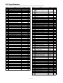
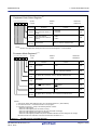
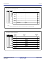
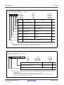
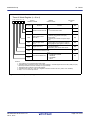
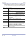
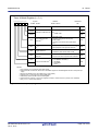
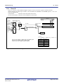
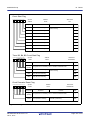
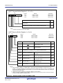
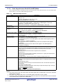
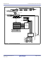
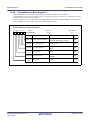
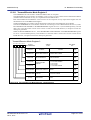
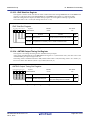
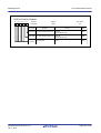
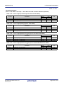
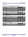
1
User’s Manual 16 M16C/6B Group User’s Manual: Hardware RENESAS MCU M16C Family / M16C/60 SERIES All information contained in these materials, including products and product specifications, represents information on the product at the time of publication and is subject to change by Renesas Electronics Corp. without notice. Please review the latest information published by Renesas Electronics Corp. through various means, including the Renesas Electronics Corp. website (http://www.renesas.com). www.renesas.com Rev.1.20 Jul 2011 Notice 1. 2. 3. 4. 5. 6. 7. All information included in this document is current as of the date this document is issued. Such information, however, is subject to change without any prior notice. Before purchasing or using any Renesas Electronics products listed herein, please confirm the latest product information with a Renesas Electronics sales office. Also, please pay regular and careful attention to additional and different information to be disclosed by Renesas Electronics such as that disclosed through our website. Renesas Electronics does not assume any liability for infringement of patents, copyrights, or other intellectual property rights of third parties by or arising from the use of Renesas Electronics products or technical information described in this document. No license, express, implied or otherwise, is granted hereby under any patents, copyrights or other intellectual property rights of Renesas Electronics or others. You should not alter, modify, copy, or otherwise misappropriate any Renesas Electronics product, whether in whole or in part. Descriptions of circuits, software and other related information in this document are provided only to illustrate the operation of semiconductor products and application examples. You are fully responsible for the incorporation of these circuits, software, and information in the design of your equipment. Renesas Electronics assumes no responsibility for any losses incurred by you or third parties arising from the use of these circuits, software, or information. When exporting the products or technology described in this document, you should comply with the applicable export control laws and regulations and follow the procedures required by such laws and regulations. You should not use Renesas Electronics products or the technology described in this document for any purpose relating to military applications or use by the military, including but not limited to the development of weapons of mass destruction. Renesas Electronics products and technology may not be used for or incorporated into any products or systems whose manufacture, use, or sale is prohibited under any applicable domestic or foreign laws or regulations. Renesas Electronics has used reasonable care in preparing the information included in this document, but Renesas Electronics does not warrant that such information is error free. Renesas Electronics assumes no liability whatsoever for any damages incurred by you resulting from errors in or omissions from the information included herein. Renesas Electronics products are classified according to the following three quality grades: “Standard”, “High Quality”, and “Specific”. The recommended applications for each Renesas Electronics product depends on the product’s quality grade, as indicated below. You must check the quality grade of each Renesas Electronics product before using it in a particular application. You may not use any Renesas Electronics product for any application categorized as “Specific” without the prior written consent of Renesas Electronics. Further, you may not use any Renesas Electronics product for any application for which it is not intended without the prior written consent of Renesas Electronics. Renesas Electronics shall not be in any way liable for any damages or losses incurred by you or third parties arising from the use of any Renesas Electronics product for an application categorized as “Specific” or for which the product is not intended where you have failed to obtain the prior written consent of Renesas Electronics. The quality grade of each Renesas Electronics product is “Standard” unless otherwise expressly specified in a Renesas Electronics data sheets or data books, etc. “Standard”: 8. 9. 10. 11. 12. Computers; office equipment; communications equipment; test and measurement equipment; audio and visual equipment; home electronic appliances; machine tools; personal electronic equipment; and industrial robots. “High Quality”: Transportation equipment (automobiles, trains, ships, etc.); traffic control systems; anti-disaster systems; anticrime systems; safety equipment; and medical equipment not specifically designed for life support. “Specific”: Aircraft; aerospace equipment; submersible repeaters; nuclear reactor control systems; medical equipment or systems for life support (e.g. artificial life support devices or systems), surgical implantations, or healthcare intervention (e.g. excision, etc.), and any other applications or purposes that pose a direct threat to human life. You should use the Renesas Electronics products described in this document within the range specified by Renesas Electronics, especially with respect to the maximum rating, operating supply voltage range, movement power voltage range, heat radiation characteristics, installation and other product characteristics. Renesas Electronics shall have no liability for malfunctions or damages arising out of the use of Renesas Electronics products beyond such specified ranges. Although Renesas Electronics endeavors to improve the quality and reliability of its products, semiconductor products have specific characteristics such as the occurrence of failure at a certain rate and malfunctions under certain use conditions. Further, Renesas Electronics products are not subject to radiation resistance design. Please be sure to implement safety measures to guard them against the possibility of physical injury, and injury or damage caused by fire in the event of the failure of a Renesas Electronics product, such as safety design for hardware and software including but not limited to redundancy, fire control and malfunction prevention, appropriate treatment for aging degradation or any other appropriate measures. Because the evaluation of microcomputer software alone is very difficult, please evaluate the safety of the final products or system manufactured by you. Please contact a Renesas Electronics sales office for details as to environmental matters such as the environmental compatibility of each Renesas Electronics product. Please use Renesas Electronics products in compliance with all applicable laws and regulations that regulate the inclusion or use of controlled substances, including without limitation, the EU RoHS Directive. Renesas Electronics assumes no liability for damages or losses occurring as a result of your noncompliance with applicable laws and regulations. This document may not be reproduced or duplicated, in any form, in whole or in part, without prior written consent of Renesas Electronics. Please contact a Renesas Electronics sales office if you have any questions regarding the information contained in this document or Renesas Electronics products, or if you have any other inquiries. (Note 1) “Renesas Electronics” as used in this document means Renesas Electronics Corporation and also includes its majorityowned subsidiaries. (Note 2) “Renesas Electronics product(s)” means any product developed or manufactured by or for Renesas Electronics. General Precautions in the Handling of MPU/MCU Products The following usage notes are applicable to all MPU/MCU products from Renesas. For detailed usage notes on the products covered by this manual, refer to the relevant sections of the manual. If the descriptions under General Precautions in the Handling of MPU/MCU Products and in the body of the manual differ from each other, the description in the body of the manual takes precedence. 1. Handling of Unused Pins Handle unused pins in accord with the directions given under Handling of Unused Pins in the manual. The input pins of CMOS products are generally in the high-impedance state. In operation with an unused pin in the open-circuit state, extra electromagnetic noise is induced in the vicinity of LSI, an associated shoot-through current flows internally, and malfunctions occur due to the false recognition of the pin state as an input signal become possible. Unused pins should be handled as described under Handling of Unused Pins in the manual. 2. Processing at Power-on The state of the product is undefined at the moment when power is supplied. The states of internal circuits in the LSI are indeterminate and the states of register settings and pins are undefined at the moment when power is supplied. In a finished product where the reset signal is applied to the external reset pin, the states of pins are not guaranteed from the moment when power is supplied until the reset process is completed. In a similar way, the states of pins in a product that is reset by an on-chip power-on reset function are not guaranteed from the moment when power is supplied until the power reaches the level at which resetting has been specified. 3. Prohibition of Access to Reserved Addresses Access to reserved addresses is prohibited. The reserved addresses are provided for the possible future expansion of functions. Do not access these addresses; the correct operation of LSI is not guaranteed if they are accessed. 4. Clock Signals After applying a reset, only release the reset line after the operating clock signal has become stable. When switching the clock signal during program execution, wait until the target clock signal has stabilized. When the clock signal is generated with an external resonator (or from an external oscillator) during a reset, ensure that the reset line is only released after full stabilization of the clock signal. Moreover, when switching to a clock signal produced with an external resonator (or by an external oscillator) while program execution is in progress, wait until the target clock signal is stable. 5. Differences between Products Before changing from one product to another, i.e. to one with a different part number, confirm that the change will not lead to problems. The characteristics of MPU/MCU in the same group but having different part numbers may differ because of the differences in internal memory capacity and layout pattern. When changing to products of different part numbers, implement a system-evaluation test for each of the products. How to Use This Manual 1. Purpose and Target Readers This manual is designed to provide the user with an understanding of the hardware functions and electrical characteristics of the MCU. It is intended for users designing application systems incorporating the MCU. A basic knowledge of electric circuits, logical circuits, and MCUs is necessary in order to use this manual. The manual comprises an overview of the product; descriptions of the CPU, system control functions, peripheral functions, and electrical characteristics; and usage notes. Particular attention should be paid to the precautionary notes when using the manual. These notes occur within the body of the text, at the end of each section, and in the Usage Notes section. The revision history summarizes the locations of revisions and additions. It does not list all revisions. Refer to the text of the manual for details. The following documents apply to the M16C/6B Group. Make sure to refer to the latest versions of these documents. The newest versions of the documents listed may be obtained from the Renesas Electronics Web site. Document Type User’s manual: Hardware Application note Renesas technical update Description Hardware specifications (pin assignments, memory maps, peripheral function specifications, electrical characteristics, timing charts) and operation description Note: Refer to the application notes for details on using peripheral functions. Information on using peripheral functions and application examples Sample programs Information on writing programs in assembly language and C Product specifications, updates on documents, etc. Document Title M16C/6B Group User’s Manual: Hardware Document No. This User’s manual Available from Renesas Electronics Web site. 2. Notation of Numbers and Symbols The notation conventions for register names, bit names, numbers, and symbols used in this manual are described below. (1) Register Names, Bit Names, and Pin Names Registers, bits, and pins are referred to in the text by symbols. The symbol is accompanied by the word “register,” “bit,” or “pin” to distinguish the three categories. Examples the PM03 bit in the PM0 register P3_5 pin, VCC pin (2) Notation of Numbers The indication “b” is appended to numeric values given in binary format. However, nothing is appended to the values of single bits. The indication “h” is appended to numeric values given in hexadecimal format. Nothing is appended to numeric values given in decimal format. Examples Binary: 11b Hexadecimal: EFA0h Decimal: 1234 3. Register Notation The symbols and terms used in register diagrams are described below. XXX Register b7 b6 b5 b4 b3 *1 b2 b1 b0 Symbol XXX 0 Bit Symbol XXX0 Address XXX Bit Name XXX bits XXX1 After Reset 00h Function RW 1 0: XXX 0 1: XXX 1 0: Do not set. 1 1: XXX RW RW (b2) Nothing is assigned. If necessary, set to 0. When read, the content is undefined. (b3) Reserved bits Set to 0. RW XXX bits Function varies according to the operating mode. RW XXX4 *3 XXX5 WO XXX6 RW XXX7 XXX bit *2 b1 b0 0: XXX 1: XXX *4 RO *1 Blank: Set to 0 or 1 according to the application. 0: Set to 0. 1: Set to 1. X: Nothing is assigned. *2 RW: Read and write. RO: Read only. WO: Write only. −: Nothing is assigned. *3 • Reserved bit Reserved bit. Set to specified value. *4 • Nothing is assigned Nothing is assigned to the bit. As the bit may be used for future functions, if necessary, set to 0. • Do not set to a value Operation is not guaranteed when a value is set. • Function varies according to the operating mode. The function of the bit varies with the peripheral function mode. Refer to the register diagram for information on the individual modes. 4. List of Abbreviations and Acronyms Abbreviation ACIA bps CRC DMA DMAC GSM Hi-Z IEBus I/O IrDA LSB MSB NC PLL PWM SIM UART VCO Full Form Asynchronous Communication Interface Adapter bits per second Cyclic Redundancy Check Direct Memory Access Direct Memory Access Controller Global System for Mobile Communications High Impedance Inter Equipment Bus Input/Output Infrared Data Association Least Significant Bit Most Significant Bit Non-Connect Phase Locked Loop Pulse Width Modulation Subscriber Identity Module Universal Asynchronous Receiver/Transmitter Voltage Controlled Oscillator All trademarks and registered trademarks are the property of their respective owners. Table of Contents SFR Page Reference ........................................................................................................................... B - 1 1. Overview ......................................................................................................................................... 1 1.1 1.1.1 1.2 1.3 1.4 1.5 1.6 2. Features ..................................................................................................................................................... 1 Applications .......................................................................................................................................... 1 Specifications ............................................................................................................................................ 2 Product List ............................................................................................................................................... 4 Block Diagram .......................................................................................................................................... 5 Pin Assignments ........................................................................................................................................ 6 Pin Functions ........................................................................................................................................... 10 Central Processing Unit (CPU) ..................................................................................................... 12 2.1 2.2 2.3 2.4 2.5 2.6 2.7 2.8 2.8.1 2.8.2 2.8.3 2.8.4 2.8.5 2.8.6 2.8.7 2.8.8 2.8.9 2.8.10 Data Registers (R0, R1, R2 and R3) ....................................................................................................... Address Registers (A0 and A1) ............................................................................................................... Frame Base Registers (FB) ...................................................................................................................... Interrupt Table Register (INTB) .............................................................................................................. Program Counter (PC) ............................................................................................................................. User Stack Pointer (USP) and Interrupt Stack Pointer (ISP) .................................................................. Static Base Register (SB) ........................................................................................................................ Flag Register (FLG) ................................................................................................................................ Carry Flag (C Flag) ............................................................................................................................. Debug Flag (D Flag) ........................................................................................................................... Zero Flag (Z Flag) ............................................................................................................................... Sign Flag (S Flag) ............................................................................................................................... Register Bank Select Flag (B Flag) .................................................................................................... Overflow Flag (O Flag) ...................................................................................................................... Interrupt Enable Flag (I Flag) ............................................................................................................. Stack Pointer Select Flag (U Flag) ..................................................................................................... Processor Interrupt Priority Level (IPL) ............................................................................................. Reserved Space ................................................................................................................................... 12 12 13 13 13 13 13 13 13 13 13 13 13 13 13 14 14 14 3. Memory ......................................................................................................................................... 15 4. Special Function Registers (SFRs) ............................................................................................... 16 5. Reset ............................................................................................................................................ 30 5.1 5.1.1 5.1.2 5.2 5.3 5.4 5.5 6. Hardware Reset ....................................................................................................................................... Reset on a Stable Supply Voltage ....................................................................................................... Power-on Reset ................................................................................................................................... Software Reset ......................................................................................................................................... Watchdog Timer Reset ............................................................................................................................ Oscillation Stop Detection Reset ............................................................................................................. Internal Space .......................................................................................................................................... 30 30 30 31 31 31 32 Processor Mode ............................................................................................................................ 33 6.1 6.2 6.3 Types of Processor Mode ........................................................................................................................ 33 Setting Processor Modes ......................................................................................................................... 33 Internal Memory ...................................................................................................................................... 35 A-1 7. Clock Generation Circuit ............................................................................................................... 36 7.1 7.1.1 7.1.2 7.1.3 7.2 7.2.1 7.2.2 7.3 7.4 7.4.1 7.4.2 7.4.3 7.4.4 7.5 7.6 7.6.1 7.6.2 7.6.3 Type of the Clock Generation Circuit ..................................................................................................... Main Clock ......................................................................................................................................... Subclock .............................................................................................................................................. 125 kHz On-Chip Oscillator Clock (fOCO-S) ................................................................................... CPU Clock and Peripheral Function Clock ............................................................................................. CPU Clock and BCLK ........................................................................................................................ Peripheral Function Clock (f1, fC32) ................................................................................................. Clock Output Function ............................................................................................................................ Power Control .......................................................................................................................................... Normal Operating Mode ..................................................................................................................... Wait Mode .......................................................................................................................................... Stop Mode ........................................................................................................................................... Power Control of Flash Memory ........................................................................................................ System Clock Protection Function .......................................................................................................... Oscillation Stop and Re-Oscillation Detect Function ............................................................................. Operation When CM27 bit = 0 (Oscillation Stop Detection Reset) ................................................... Operation When CM27 bit = 1 (Oscillation Stop and Re-oscillation Detect Interrupt) ..................... How to Use Oscillation Stop and Re-Oscillation Detect Function ..................................................... 36 42 43 43 44 44 45 45 46 46 48 50 53 58 59 59 59 60 8. Protection ...................................................................................................................................... 61 9. Interrupt ........................................................................................................................................ 62 9.1 9.2 9.2.1 9.2.2 9.2.3 9.2.4 9.3 9.3.1 9.3.2 9.4 9.4.1 9.4.2 9.5 9.5.1 9.5.2 9.5.3 9.5.4 9.5.5 9.5.6 9.5.7 9.5.8 9.5.9 9.5.10 9.6 9.7 9.8 Type of Interrupts .................................................................................................................................... Software Interrupts .................................................................................................................................. Undefined Instruction Interrupt .......................................................................................................... Overflow Interrupt .............................................................................................................................. BRK Interrupt ..................................................................................................................................... INT Instruction Interrupt .................................................................................................................... Hardware Interrupts ................................................................................................................................. Special Interrupts ................................................................................................................................ Peripheral Function Interrupts ............................................................................................................ Interrupts and Interrupt Vector ................................................................................................................ Fixed Vector Tables ............................................................................................................................ Relocatable Vector Tables .................................................................................................................. Interrupt Control ...................................................................................................................................... I Flag ................................................................................................................................................... IR Bit ................................................................................................................................................... Bits ILVL2 to ILVL0 and IPL ............................................................................................................ Interrupt Sequence .............................................................................................................................. Interrupt Response Time ..................................................................................................................... Variation of IPL When Interrupt Request IS Accepted ...................................................................... Saving Registers ................................................................................................................................. Returning from an Interrupt Routine .................................................................................................. Interrupt Priority ................................................................................................................................. Interrupt Priority Level Select Circuit ................................................................................................ INT Interrupt ........................................................................................................................................... NMI Interrupt .......................................................................................................................................... Key Input Interrupt .................................................................................................................................. A-2 62 63 63 63 63 63 64 64 64 65 65 66 68 70 70 70 71 72 72 73 74 74 74 76 77 77 9.9 10. Address Match Interrupt .......................................................................................................................... 80 Watchdog Timer ............................................................................................................................ 82 10.1 10.2 11. Count Source Protection Mode Disabled ................................................................................................ 85 Count Source Protection Mode Enabled ................................................................................................. 86 DMAC ........................................................................................................................................... 87 11.1 11.1.1 11.1.2 11.2 11.3 11.4 11.5 12. Transfer Cycles ........................................................................................................................................ Effect of Source and Destination Addresses ....................................................................................... Effect of Software Wait ...................................................................................................................... DMA Transfer Cycles ............................................................................................................................. DMA Enabled .......................................................................................................................................... DMA Request .......................................................................................................................................... Channel Priority and DMA Transfer Timing .......................................................................................... Timers .......................................................................................................................................... 98 12.1 Timer A ................................................................................................................................................. 12.1.1 Timer A I/O Function ....................................................................................................................... 12.1.2 Timer Mode ...................................................................................................................................... 12.1.3 Event Counter Mode ......................................................................................................................... 12.1.4 One-Shot Timer Mode ...................................................................................................................... 12.1.5 Pulse Width Modulation (PWM Mode) (Only i = 0 or 1 in the 48-Pin Version) ............................. 12.2 Timer B .................................................................................................................................................. 12.2.1 Timer Mode ...................................................................................................................................... 12.2.2 Event Counter Mode ......................................................................................................................... 13. 93 93 93 95 96 96 97 101 102 109 111 115 117 120 124 125 Serial Interface ............................................................................................................................ 126 13.1 UARTi (i = 0 to 2) ................................................................................................................................. 126 13.1.1 Clock Synchronous Serial I/O Mode ................................................................................................ 140 13.1.2 Clock Asynchronous Serial I/O (UART) Mode ............................................................................... 148 13.1.3 Special Mode 1 (I2C mode) .............................................................................................................. 156 13.1.4 Special Mode 2 ................................................................................................................................. 166 13.1.5 Special Mode 3 (IE mode) ................................................................................................................ 170 13.1.6 Special Mode 4 (SIM Mode) (UART2) ............................................................................................ 172 14. A/D Converter (64-Pin Version Only) .......................................................................................... 177 14.1 14.1.1 14.1.2 14.1.3 14.1.4 14.1.5 14.2 14.3 14.4 15. Mode Description .................................................................................................................................. One-Shot Mode ................................................................................................................................. Repeat Mode ..................................................................................................................................... Single Sweep Mode .......................................................................................................................... Repeat Sweep Mode 0 ...................................................................................................................... Repeat Sweep Mode 1 ...................................................................................................................... Conversion Rate .................................................................................................................................... Current Consumption Reducing Function ............................................................................................. Output Impedance of Sensor under A/D Conversion ............................................................................ 181 181 183 185 187 189 191 191 192 Baseband Functionality .............................................................................................................. 193 15.1 Baseband Functional Description .......................................................................................................... 193 15.1.1 Baseband Block Diagram ................................................................................................................. 194 A-3 15.1.2 Baseband Terminological Description .............................................................................................. 15.1.3 26-Bit Timer ..................................................................................................................................... 15.1.4 Transmit RAM .................................................................................................................................. 15.1.5 Receive RAM ................................................................................................................................... 15.1.6 Transmit Frame Generator ................................................................................................................ 15.1.7 Filter Function ................................................................................................................................... 15.1.8 Interrupts ........................................................................................................................................... 15.1.9 CRC Circuit ...................................................................................................................................... 15.1.10 Automatic ACK Response Function ................................................................................................. 15.1.11 Automatic ACK Reception Function ................................................................................................ 15.1.12 Automatic Reception Switching Function ........................................................................................ 15.1.13 ANTSW Output Switching Function ................................................................................................ 15.1.14 Automatic CSMA-CA Function ....................................................................................................... 15.1.15 State Transitions ............................................................................................................................... 15.2 Baseband Associated Registers ............................................................................................................. 15.2.1 Baseband Control Register ............................................................................................................... 15.2.2 Transmit/Receive Reset Register ...................................................................................................... 15.2.3 Transmit/Receive Mode Register 0 .................................................................................................. 15.2.4 Transmit/Receive Mode Register 1 .................................................................................................. 15.2.5 Receive Frame Length Register ........................................................................................................ 15.2.6 Receive Data Counter Register ......................................................................................................... 15.2.7 RSSI/CCA Result Register ............................................................................................................... 15.2.8 Transmit/Receive Status Register 0 .................................................................................................. 15.2.9 Transmit Frame Length Register ...................................................................................................... 15.2.10 Transmit/Receive Mode Register 2 .................................................................................................. 15.2.11 Transmit/Receive Mode Register 3 .................................................................................................. 15.2.12 Receive Level Threshold Set Register .............................................................................................. 15.2.13 Transmit/Receive Control Register .................................................................................................. 15.2.14 CSMA Control Register 0 ................................................................................................................. 15.2.15 CCA Threshold Level Set Register .................................................................................................. 15.2.16 Transmit/Receive Status Register 1 .................................................................................................. 15.2.17 RF Control Register .......................................................................................................................... 15.2.18 Transmit/Receive Mode Register 4 .................................................................................................. 15.2.19 CSMA Control Register 1 ................................................................................................................. 15.2.20 CSMA Control Register 2 ................................................................................................................. 15.2.21 PAN Identifier Register .................................................................................................................... 15.2.22 Short Address Register ..................................................................................................................... 15.2.23 Extended Address Register ............................................................................................................... 15.2.24 Timer Read-Out Register .................................................................................................................. 15.2.25 Timer Compare i (i = 0 to 2) Register .............................................................................................. 15.2.26 Time Stamp Registers ....................................................................................................................... 15.2.27 Timer Control Register ..................................................................................................................... 15.2.28 Backoff Period Register .................................................................................................................... 15.2.29 PLL Division Registers ..................................................................................................................... 15.2.30 Transmit Output Power Register ...................................................................................................... 15.2.31 RSSI Offset Register ......................................................................................................................... 15.2.32 Verification Mode Set Register ........................................................................................................ 15.2.33 IDLE Wait Set Register .................................................................................................................... 15.2.34 ANTSW Output Timing Set Register ............................................................................................... 15.2.35 RF Initial Set Register ....................................................................................................................... A-4 194 195 196 196 197 198 199 200 201 203 204 204 205 207 208 208 209 210 211 212 212 213 214 215 216 217 218 218 219 219 220 221 222 223 223 224 225 225 226 227 228 229 229 230 231 232 233 234 234 235 15.3 Control Sequence .................................................................................................................................. 15.3.1 Transmission Procedure Example .................................................................................................... 15.3.2 Reception Procedure Example .......................................................................................................... 15.3.3 CCA Procedure Example .................................................................................................................. 15.3.4 CSMA-CA Procedure Example ........................................................................................................ 15.3.5 Baseband Startup Procedure Example .............................................................................................. 15.3.6 Baseband Shutdown Procedure Example ......................................................................................... 15.3.7 Examples of Automatic Transmit and Receive Operations .............................................................. 236 236 236 237 237 238 238 239 16. CRC Operation ........................................................................................................................... 240 17. Programmable I/O Ports ............................................................................................................. 242 17.1 17.2 17.3 17.4 18. Port Pi Direction Register (PDi Register, i = 5 to 8, 10) ....................................................................... Port Pi Register (Pi Register, i = 5 to 8, 10) .......................................................................................... Pull-up Control Register 1 to Pull-up Control Register 2 (Registers PUR1 to PUR2) ......................... LED Port Switch Register (LEDCON Register) ................................................................................... Flash Memory ............................................................................................................................. 251 18.1 18.1.1 18.1.2 18.2 18.2.1 18.2.2 18.2.3 18.2.4 18.3 18.3.1 18.3.2 18.3.3 18.3.4 18.3.5 18.3.6 18.3.7 18.4 18.4.1 18.4.2 18.5 18.5.1 18.6 18.6.1 18.6.2 18.6.3 18.6.4 19. 19.1 242 242 242 242 Memory Map ......................................................................................................................................... Boot Mode ........................................................................................................................................ User Boot Function ........................................................................................................................... Functions to Prevent Flash Memory from Rewriting ............................................................................ ROM Code Protect Function ............................................................................................................ ID Code Check Function .................................................................................................................. Forced Erase Function ...................................................................................................................... Standard Serial I/O Mode Disable Function ..................................................................................... CPU Rewrite Mode ............................................................................................................................... EW0 Mode ........................................................................................................................................ EW1 Mode ........................................................................................................................................ Flash Memory Control Register (Registers FMR0, FMR1, FMR2 and FMR6) .............................. Software Commands ......................................................................................................................... Data Protect Function ....................................................................................................................... Status Register .................................................................................................................................. Full Status Check .............................................................................................................................. Standard Serial I/O Mode ...................................................................................................................... ID Code Check Function .................................................................................................................. Example of Circuit Application in the Standard Serial I/O Mode .................................................... Parallel I/O Mode .................................................................................................................................. ROM Code Protect Function ............................................................................................................ Notes on Flash Memory ........................................................................................................................ Functions to Prevent Flash Memory from Being Rewritten ............................................................. Reading Data Flash ........................................................................................................................... CPU Rewrite Mode ........................................................................................................................... User Boot Mode ................................................................................................................................ 252 253 253 255 255 255 256 256 258 259 259 260 267 273 273 275 277 277 281 283 283 284 284 284 284 285 Electrical Characteristics ............................................................................................................ 286 Electrical Characteristics ....................................................................................................................... 286 A-5 20. Precautions ................................................................................................................................. 305 20.1 SFR ........................................................................................................................................................ 20.1.1 Register Settings ............................................................................................................................... 20.2 Reset ...................................................................................................................................................... 20.2.1 VCC .................................................................................................................................................. 20.2.2 CNVSS .............................................................................................................................................. 20.3 Baseband Functions ............................................................................................................................... 20.4 Power Control ........................................................................................................................................ 20.5 Interrupt ................................................................................................................................................. 20.5.1 Reading address 00000h ................................................................................................................... 20.5.2 SP Setting .......................................................................................................................................... 20.5.3 NMI Interrupt .................................................................................................................................... 20.5.4 Changing an Interrupt Generate Factor ............................................................................................ 20.5.5 INT Interrupt ..................................................................................................................................... 20.5.6 Rewriting the Interrupt Control Register .......................................................................................... 20.5.7 Watchdog Timer Interrupt ................................................................................................................ 20.6 DMAC ................................................................................................................................................... 20.6.1 Write to the DMAE Bit in the DMiCON Register (i = 0 to 3) ......................................................... 20.7 Timers .................................................................................................................................................... 20.7.1 Timer A ............................................................................................................................................. 20.7.2 Timer B ............................................................................................................................................. 20.8 Serial Interface ...................................................................................................................................... 20.8.1 Clock Synchronous Serial I/O .......................................................................................................... 20.8.2 UART (Clock Asynchronous Serial I/O) Mode ............................................................................... 20.8.3 Special Mode 1 (I2C Mode) .............................................................................................................. 20.8.4 Special Mode 4 (SIM Mode) ............................................................................................................ 20.8.5 Common Items for Multiple Modes ................................................................................................. 20.9 A/D Converter (64-Pin Version Only) .................................................................................................. 20.10 Notes on Flash Memory ........................................................................................................................ 20.10.1 Functions to Prevent Flash Memory from Being Rewritten ............................................................. 20.10.2 Reading Data Flash ........................................................................................................................... 20.10.3 CPU Rewrite Mode ........................................................................................................................... 20.10.4 User Boot Mode ................................................................................................................................ 20.11 Noise ...................................................................................................................................................... 305 305 306 306 306 307 308 310 310 310 310 311 311 312 313 314 314 315 315 319 321 321 323 323 323 323 324 326 326 326 326 327 328 Appendix 1. Package Dimensions ........................................................................................................ 329 Index ..................................................................................................................................................... 330 A-6 SFR Page Reference The following tables only indicate where registers first appear. Refer to the index for registers that appear multiple times. Address 0000h 0001h 0002h 0003h 0004h 0005h 0006h 0007h 0008h 0009h 000Ah 000Bh 000Ch 000Dh 000Eh 000Fh 0010h 0011h 0012h 0013h 0014h 0015h 0016h 0017h 0018h 0019h 001Ah 001Bh 001Ch 001Dh 001Eh 001Fh 0020h 0021h 0022h 0023h 0024h 0025h 0026h 0027h 0028h 0029h 002Ah 002Bh 002Ch 002Dh 002Eh 002Fh 0030h 0031h 0032h 0033h 0034h 0035h 0036h 0037h 0038h 0039h 003Ah 003Bh 003Ch 003Dh 003Eh 003Fh 0040h 0041h 0042h 0043h 0044h Register Processor Mode Register 0 Processor Mode Register 1 System Clock Control Register 0 System Clock Control Register 1 Symbol PM0 PM1 CM0 CM1 Page 33 34 38 39 Protect Register PRCR 61 Oscillation Stop Detection Register CM2 40 Program 2 Area Control Register PRG2C 34 Peripheral Clock Select Register PCLKR 41 Clock Prescaler Reset Flag CPSRF 107 Processor Mode Register 2 PM2 41 Address 0045h 0046h 0047h 0048h 0049h 004Ah 004Bh 004Ch 004Dh 004Eh 004Fh 0050h 0051h 0052h 0053h 0054h 0055h 0056h 0057h 0058h 0059h 005Ah 005Bh 005Ch 005Dh 005Eh 005Fh 0060h 0061h 0062h 0063h 0064h 0065h 0066h 0067h 0068h 0069h 006Ah 006Bh 006Ch 006Dh 006Eh 006Fh 0070h 0071h 0072h 0073h 0074h 0075h 0076h 0077h 0078h 0079h 007Ah 007Bh 007Ch 007Dh 007Eh 007Fh 0080h 0081h 0082h 0083h 0084h 0085h to 00FFh Register Timer B5 Interrupt Control Register Timer B4 Interrupt Control Register, UART1 BUS Collision Detection Interrupt Control Register Timer B3 Interrupt Control Register, UART0 BUS Collision Detection Interrupt Control Register Timer Compare 0 Interrupt Control Register Timer Compare 1 Interrupt Control Register UART2 BUS Collision Detection Interrupt Control Register Symbol TB5IC TB4IC, U1BCNIC 68 TB3IC, U0BCNIC 68 BBTIM0IC BBTIM1IC BCNIC 68 68 DMA0 Interrupt Control Register DMA1 Interrupt Control Register Key Input Interrupt Control Register A/D Conversion Interrupt Control Register UART2 Transmit Interrupt Control Register UART2 Receive Interrupt Control Register UART0 Transmit Interrupt Control Register UART0 Receive Interrupt Control Register UART1 Transmit Interrupt Control Register UART1 Receive Interrupt Control Register Timer A0 Interrupt Control Register Timer A1 Interrupt Control Register Timer A2 Interrupt Control Register Timer A3 Interrupt Control Register Timer A4 Interrupt Control Register Timer B0 Interrupt Control Register Timer B1 Interrupt Control Register Timer B2 Interrupt Control Register INT0 Interrupt Control Register INT1 Interrupt Control Register Timer Compare 2 Interrupt Control Register DM0IC DM1IC KUPIC ADIC S2TIC S2RIC S0TIC S0RIC S1TIC S1RIC TA0IC TA1IC TA2IC TA3IC TA4IC TB0IC TB1IC TB2IC INT0IC INT1IC BBTIM2IC 68 68 68 68 68 68 68 68 68 68 68 68 68 68 68 68 68 68 69 69 68 DMA2 Interrupt Control Register DMA3 Interrupt Control Register Transmit Complete Interrupt Control Register Bank 0 Receive Complete/IDLE Interrupt Control Register Bank 1 Receive Complete/Clock Regulator Interrupt Control Register Address Filter Interrupt Control Register CCA Complete Interrupt Control Register PLL Lock Detection Interrupt Control Register Transmit Overrun Interrupt Control Register Receive Overrun 0 Interrupt Control Register Receive Overrun 1 Interrupt Control Register DM2IC DM3IC BBTXIC 68 68 LED Port Switch Register LEDCON 249 Key Input Control Register 0 Key Input Control Register 1 Timer A I/O Control Register KICON0 KICON1 TAICON 79 79 102 BBRX0IC/ BBIDLEIC BBRX1IC/ BBCREGIC BBADFIC BBCCAIC BBPLLIC BBTXORIC BBRXOR0IC BBRXOR1IC Blank columns are all reserved space. No access is allowed. B-1 Page 68 68 68 68 68 68 68 68 68 68 68 Address 0100h 0101h 0102h 0103h 0104h 0105h 0106h 0107h 0108h 0109h 010Ah 010Bh 010Ch 010Dh 010Eh 010Fh 0110h 0111h 0112h 0113h 0114h 0115h 0116h 0117h 0118h 0119h 011Ah 011Bh 011Ch 011Dh 011Eh 011Fh 0120h 0121h 0122h 0123h 0124h 0125h 0126h 0127h 0128h 0129h 012Ah 012Bh 012Ch 012Dh 012Eh 012Fh 0130h 0131h 0132h 0133h 0134h 0135h 0136h 0137h 0138h 0139h 013Ah 013Bh 013Ch 013Dh 013Eh 013Fh 0140h 0141h 0142h 0143h Register Baseband Control Register Transmit/Receive Reset Register Transmit/Receive Mode Register 0 Transmit/Receive Mode Register 1 Receive Frame Length Register Receive Data Counter Register RSSI/CCA Result Register Transmit/Receive Status Register 0 Transmit Frame Length Register Transmit/Receive Mode Register 2 Transmit/Receive Mode Register 3 Receive Level Threshold Set Register Transmit/Receive Control Register CSMA Control Register 0 CCA Threshold Level Set Register Transmit/Receive Status Register 1 RF Control Register Transmit/Receive Mode Register 4 CSMA Control Register 1 CSMA Control Register 2 PAN Identifier Register Symbol BBCON BBTXRXRST BBTXRXMODE0 BBTXRXMODE1 BBRXFLEN BBRXCOUNT BBRSSICCARSLT BBTXRXST0 BBTXFLEN BBTXRXMODE2 BBTXRXMODE3 BBLVLVTH BBTXRXCON BBCSMACON0 BBCCAVTH BBTXRXST1 BBRFCON BBTXRXMODE4 BBCSMACON1 BBCSMACON2 BBPANID Short Address Register BBSHORTAD Expansion Address Register BBEXTENDAD0 BBEXTENDAD1 BBEXTENDAD2 BBEXTENDAD3 Timer Read-Out Register 0 BBTIMEREAD0 Timer Read-Out Register 1 BBTIMEREAD1 Timer Compare 0 Register 0 BBTCOMP0REG0 Timer Compare 0 Register 1 BBTCOMP0REG1 Timer Compare 1 Register 0 BBTCOMP1REG0 Timer Compare 1 Register 1 BBTCOMP1REG1 Timer Compare 2 Register 0 BBTCOMP2REG0 Timer Compare 2 Register 1 BBTCOMP2REG1 Time Stamp Register 0 BBTSTAMP0 Time Stamp Register 1 BBTSTAMP1 Timer Control Register Backoff Period Register BBTIMECON BBBOFFPROD PLL Division Register 0 PLL Division Register 1 Transmit Output Power Register RSSI Offset Register BBPLLDIVL BBPLLDIVH BBTXOUTPWR BBRSSIOFS Page 208 209 210 211 212 212 213 214 215 216 217 218 218 219 219 220 221 222 223 223 224 225 225 225 225 225 226 226 227 227 227 227 227 227 228 228 229 229 230 230 231 232 Address 0144h 0145h 0146h 0147h 0148h 0149h 014Ah 014Bh 014Ch 014Dh 014Eh 014Fh 0150h 0151h 0152h 0153h 0154h 0155h 0156h 0157h 0158h 0159h 015Ah 015Bh 015Ch 015Dh 015Eh 015Fh 0160h 0161h 0162h 0163h 0164h 0165h 0166h 0167h 0168h 0169h 016Ah 016Bh 016Ch 016Dh 016Eh 016Fh 0170h 0171h 0172h 0173h 0174h 0175h 0176h 0177h 0178h 0179h 017Ah 017Bh 017Ch 017Dh 017Eh 017Fh 0180h 0181h 0182h 0183h 0184h 0185h 0186h 0187h Register Symbol Verification Mode Set Register BBEVAREG 233 IDLE Wait Set Register BBIDLEWAIT 234 ANTSW Output Timing Set Register BBANTSWTIMG 234 RF Initial Set Register BBRFINI DMA0 Source Pointer SAR0 235 91 DMA0 Destination Pointer DAR0 Blank columns are all reserved space. No access is allowed. B-2 Page 92 Address 0188h 0189h 018Ah 018Bh 018Ch 018Dh 018Eh 018Fh 0190h 0191h 0192h 0193h 0194h 0195h 0196h 0197h 0198h 0199h 019Ah 019Bh 019Ch 019Dh 019Eh 019Fh 01A0h 01A1h 01A2h 01A3h 01A4h 01A5h 01A6h 01A7h 01A8h 01A9h 01AAh 01ABh 01ACh 01ADh 01AEh 01AFh 01B0h 01B1h 01B2h 01B3h 01B4h 01B5h 01B6h 01B7h 01B8h 01B9h 01BAh 01BBh 01BCh 01BDh 01BEh 01BFh 01C0h 01C1h 01C2h 01C3h 01C4h 01C5h 01C6h 01C7h 01C8h 01C9h 01CAh 01CBh Register DMA0 Transfer Counter Symbol TCR0 DMA0 Control Register DM0CON Page 92 Address 01CCh 01CDh 01CEh Register Symbol Page 01CFh DMA1 Source Pointer 91 01D0h Timer A Count Source Select Register 0 TACS0 107 01D1h Timer A Count Source Select Register 1 TACS1 107 01D2h Timer A Count Source Select Register 2 TACS2 108 Timer A Waveform Output Function Select Register TAPOFS 01E8h Timer B Count Source Select Register 2 TBCS2 123 01E9h Timer B Count Source Select Register 3 TBCS3 123 0206h Interrupt Source Select Register 2 IFSR2A 76 0207h Interrupt Source Select Register IFSR 76 01D3h SAR1 91 01D4h 01D5h DMA1 Destination Pointer 108 01D6h DAR1 92 01D7h 01D8h 01D9h DMA1 Transfer Counter TCR1 92 01DAh 01DBh 01DEh 01DCh DMA1 Control Register DM1CON 91 01DDh 01DFh 01E0h DMA2 Source Pointer 01E1h SAR2 91 01E2h 01E3h 01E4h DMA2 Destination Pointer DAR2 01E5h 92 01E6h 01E7h DMA2 Transfer Counter TCR2 92 01EAh 01EBh DMA2 Control Register DM2CON 91 01ECh 01EDh 01EEh 01EFh DMA3 Source Pointer SAR3 01F0h 91 01F1h 01F2h DMA3 Destination Pointer 01F3h DAR3 92 01F4h 01F5h 01F6h DMA3 Transfer Counter TCR3 01F7h 92 01F8h 01F9h 01FAh DMA3 Control Register DM3CON 91 01FBh 01FCh 01FDh 01FEh 01FFh 0200h 0201h 0202h 0203h 0204h 0205h Timer B Count Source Select Register 0 Timer B Count Source Select Register 1 TBCS0 TBCS1 123 123 0208h 0209h 020Ah 020Bh 020Ch 020Dh 020Eh Address Match Interrupt Enable Register AIER 81 020Fh Address Match Interrupt Enable Register 2 AIER2 81 Blank columns are all reserved space. No access is allowed. B-3 Address 0210h 0211h 0212h 0213h 0214h 0215h 0216h 0217h 0218h 0219h 021Ah 021Bh 021Ch 021Dh 021Eh 021Fh 0220h 0221h 0222h 0223h 0224h 0225h 0226h 0227h 0228h 0229h 022Ah 022Bh 022Ch 022Dh 022Eh 022Fh 0230h 0231h 0232h 0233h 0234h 0235h 0236h 0237h 0238h 0239h 023Ah 023Bh 023Ch 023Dh 023Eh 023Fh 0240h 0241h 0242h 0243h 0244h 0245h 0246h 0247h 0248h 0249h 024Ah 024Bh 024Ch 024Dh 024Eh 024Fh Register Address Match Interrupt Register 0 Symbol RMAD0 Page 81 Address Match Interrupt Register 1 RMAD1 81 Address Match Interrupt Register 2 RMAD2 81 Address Match Interrupt Register 3 RMAD3 81 Flash Memory Control Register 0 Flash Memory Control Register 1 Flash Memory Control Register 2 FMR0 FMR1 FMR2 260 262 263 Flash Memory Control Register 6 FMR6 264 UART0 Special Mode Register 4 UART0 Special Mode Register 3 UART0 Special Mode Register 2 UART0 Special Mode Register UART0 Transmit/Receive Mode Register UART0 Bit Rate Register UART0 Transmit Buffer Register U0SMR4 U0SMR3 U0SMR2 U0SMR U0MR U0BRG U0TB 139 138 137 136 131 131 UART0 Transmit/Receive Control Register 0 U0C0 UART0 Transmit/Receive Control Register 1 U0C1 UART0 Receive Buffer Register U0RB 130 132 133 130 Address 0250h 0251h 0252h 0253h 0254h 0255h 0256h 0257h 0258h 0259h 025Ah 025Bh 025Ch 025Dh 025Eh 025Fh 0260h 0261h 0262h 0263h 0264h 0265h 0266h 0267h 0268h 0269h 026Ah 026Bh 026Ch 026Dh 026Eh 026Fh 0270h 0271h 0272h 0273h 0274h 0275h 0276h 0277h 0278h 0279h 027Ah 027Bh 027Ch 027Dh 027Eh 027Fh 0280h 0281h 0282h 0283h 0284h 0285h 0286h 0287h 0288h 0289h 028Ah 028Bh 028Ch 028Dh 028Eh 028Fh 0290h to 02FFh Register UART Transmit/Receive Control Register 2 Symbol UCON UART1 Special Mode Register 4 UART1 Special Mode Register 3 UART1 Special Mode Register 2 UART1 Special Mode Register UART1 Transmit/Receive Mode Register UART1 Bit Rate Register UART1 Transmit Buffer Register U1SMR4 U1SMR3 U1SMR2 U1SMR U1MR U1BRG U1TB 139 138 137 136 131 131 130 UART1 Transmit/Receive Control Register 0 U1C0 UART1 Transmit/Receive Control Register 1 U1C1 UART1 Receive Buffer Register U1RB 132 133 UART2 Special Mode Register 4 UART2 Special Mode Register 3 UART2 Special Mode Register 2 UART2 Special Mode Register UART2 Transmit/Receive Mode Register UART2 Bit Rate Register UART2 Transmit Buffer Register U2SMR4 U2SMR3 U2SMR2 U2SMR U2MR U2BRG U2TB 139 138 137 136 131 131 UART2 Transmit/Receive Control Register 0 UART2 Transmit/Receive Control Register 1 UART2 Receive Buffer Register U2C0 U2C1 U2RB 132 134 Blank columns are all reserved space. No access is allowed. B-4 Page 135 130 130 130 Address 0300h 0301h 0302h 0303h 0304h 0305h 0306h 0307h 0308h 0309h 030Ah 030Bh 030Ch 030Dh 030Eh 030Fh 0310h 0311h 0312h 0313h 0314h 0315h 0316h 0317h 0318h 0319h 031Ah 031Bh 031Ch 031Dh 031Eh 031Fh 0320h 0321h 0322h 0323h 0324h 0325h 0326h 0327h 0328h 0329h 032Ah 032Bh 032Ch 032Dh 032Eh 032Fh 0330h 0331h 0332h 0333h 0334h 0335h 0336h 0337h 0338h 0339h 033Ah 033Bh 033Ch 033Dh 033Eh 033Fh 0340h 0341h 0342h 0343h 0344h Register Timer B3, B4, B5 Count Start Flag Symbol TBSR Page 122 Timer B3 Register TB3 Timer B4 Register TB4 Timer B5 Register TB5 Timer B3 Mode Register Timer B4 Mode Register Timer B5 Mode Register TB3MR TB4MR TB5MR 121 121 121 Count Start Flag TABSR 105 One-Shot Start Flag Trigger Select Register Up/Down Flag ONSF TRGSR UDF 106 106 105 Timer A0 Register TA0 Timer A1 Register TA1 Timer A2 Register TA2 Timer A3 Register TA3 Timer A4 Register TA4 Timer B0 Register TB0 Timer B1 Register TB1 Timer B2 Register TB2 Timer A0 Mode Register Timer A1 Mode Register Timer A2 Mode Register Timer A3 Mode Register Timer A4 Mode Register Timer B0 Mode Register Timer B1 Mode Register Timer B2 Mode Register TA0MR TA1MR TA2MR TA3MR TA4MR TB0MR TB1MR TB2MR 121 121 121 104 104 104 104 104 121 121 121 103 103 103 103 103 121 121 121 Address 0345h 0346h 0347h 0348h 0349h 034Ah 034Bh 034Ch 034Dh 034Eh 034Fh 0350h 0351h 0352h 0353h 0354h 0355h 0356h 0357h 0358h 0359h 035Ah 035Bh 035Ch 035Dh 035Eh 035Fh 0360h 0361h 0362h 0363h 0364h 0365h 0366h 0367h 0368h 0369h 036Ah 036Bh 036Ch 036Dh 036Eh 036Fh 0370h 0371h 0372h 0373h 0374h 0375h 0376h 0377h 0378h 0379h 037Ah 037Bh 037Ch 037Dh 037Eh 037Fh 0380h 0381h 0382h 0383h 0384h 0385h 0386h 0387h Register Symbol Pull-Up Control Register 1 Pull-Up Control Register 2 PUR1 PUR2 248 248 Count Source Protection Mode Register Watchdog Timer Reset Register Watchdog Timer Start Register Watchdog Timer Control Register CSPR WDTR WDTS WDC 84 83 83 83 Blank columns are all reserved space. No access is allowed. B-5 Page Address 0388h 0389h 038Ah 038Bh 038Ch 038Dh 038Eh 038Fh 0390h 0391h 0392h 0393h 0394h 0395h 0396h 0397h 0398h 0399h 039Ah 039Bh 039Ch 039Dh 039Eh 039Fh 03A0h 03A1h 03A2h 03A3h 03A4h 03A5h 03A6h 03A7h 03A8h 03A9h 03AAh 03ABh 03ACh 03ADh 03AEh 03AFh 03B0h 03B1h 03B2h 03B3h 03B4h 03B5h 03B6h 03B7h 03B8h 03B9h 03BAh 03BBh 03BCh 03BDh 03BEh 03BFh 03C0h 03C1h 03C2h 03C3h 03C4h 03C5h 03C6h 03C7h 03C8h 03C9h 03CAh 03CBh Register Symbol Page DMA2 Source Select Register DM2SL 89 DMA3 Source Select Register DM3SL 89 DMA0 Source Select Register DM0SL 89 DMA1 Source Select Register DM1SL 89 CRC Data Register CRCD CRC Input Register CRCIN A/D Register 0 AD0 A/D Register 1 AD1 A/D Register 2 AD2 A/D Register 3 AD3 A/D Register 4 AD4 A/D Register 5 AD5 240 240 180 180 180 Address 03CCh 03CDh 03CEh 03CFh 03D0h 03D1h 03D2h 03D3h 03D4h 03D5h 03D6h 03D7h 03D8h 03D9h 03DAh 03DBh 03DCh 03DDh 03DEh 03DFh 03E0h 03E1h 03E2h 03E3h 03E4h 03E5h 03E6h 03E7h 03E8h 03E9h 03EAh 03EBh 03ECh 03EDh 03EEh 03EFh 03F0h 03F1h 03F2h 03F3h 03F4h 03F5h 03F6h 03F7h 03F8h 03F9h 03FAh 03FBh 03FCh 03FDh 03FEh 03FFh D000h to D09Fh D100h to D17Eh Register Page AD6 A/D Register 7 AD7 A/D Control Register 2 ADCON2 180 A/D Control Register 0 A/D Control Register 1 ADCON0 ADCON1 179 179 Port P5 Register P5 247 Port P5 Direction Register Port P6 Register Port P7 Register Port P6 Direction Register Port P7 Direction Register Port P8 Register PD5 P6 P7 PD6 PD7 P8 246 247 247 246 246 247 Port P8 Direction Register PD8 246 Port P10 Register P10 247 Port P10 Direction Register PD10 246 Transmit RAM TRANSMIT_RAM_ START 180 180 TRANSMIT_RAM_ END D17Fh D180h to D1FEh Receive RAM RECIEVE_RAM_ START RECIEVE_RAM_ END 180 180 Symbol A/D Register 6 D1FFh to D7FFh 180 FFFFFh Option Function Select Address OFS1 Blank columns are all reserved space. No access is allowed. B-6 84 M16C/6B Group RENESAS MCU 1. R01UH0197EJ0120 Rev.1.20 Jul 21, 2011 Overview 1.1 Features The M16C/6B Group microcomputers (MCUs) incorporate the M16C/60 Series CPU core and flash memory. These MCUs also function as low-power-consumption transceivers which support near field communication (2.4 GHz band). Integrating some of the physical (PHY) and MAC layers compliant to the IEEE802.15.4 standard, the MUCs support various applications ranging from simple communication systems to mesh network systems. 1.1.1 Applications Home automation, Building automation, Factory automation, Wireless sensor networks, RF remote controllers R01UH0197EJ0120 Rev.1.20 Jul 21, 2011 Page 1 of 331 M16C/6B Group 1.2 1. Overview Specifications Tables 1.1 and 1.2 list Specifications Outline. Table 1.1 Item RF CPU Memory Clock Specifications (1) Function RF frequency Reception sensitivity Transmission output level Central processing unit ROM, RAM, data flash Clock generation circuits Specification 2405 MHz to 2480 MHz −94 dBm 0 dBm • M16C/60 core (Multiplier: 16 bits × 16 bits → 32 bits, multiply and accumulate instruction: 16 bits × 16 bits + 32 bits → 32 bits) • Number of basic instructions: 91 • Minimum instruction execution time: 62.5 ns (f(BCLK) = 16 MHz, VCC = 2.7 V to 3.6 V) • Operating mode: Single-chip mode Refer to Table 1.3 “Product List”. • 3 circuits: Main clock, subclock, on-chip oscillator (125 kHz) • Oscillation stop detection: Main clock oscillation stop and re-oscillation detection function • Frequency divider circuit: Divide ratio selectable from 1, 2, 4, 8, and 16 • Low-power-consumption modes: Wait mode, stop mode I/O ports Programmable I/O • CMOS I/O ports: 30 (64-pin version), ports 16 (48-pin version), selectable pull-up resistor • Nch open drain ports: 3 Interrupts • Number of interrupt vectors: 70 • External interrupt input: 11 (NMI, INT × 2, key input × 8 (64-pin version), key input × 4 (48-pin version)) • Priority levels: 7 levels Watchdog timer 15 bits × 1 (with prescaler), selectable reset start function DMA DMAC • 4 channels, cycle steal mode • Trigger sources: 43 • Transfer modes: 2 (single transfer, repeat transfer) Timer Timer A • 16-bit timer × 5 (64-pin version), 16-bit timer × 2 (48-pin version): Timer mode, event counter mode, one-shot timer mode, pulse width modulation (PWM) mode • 16-bit timer × 3 (48-pin version): Timer mode Timer B 16-bit timer × 6: Timer mode Serial interface UART0 to UART2 Clock synchronous/asynchronous × 3 channels A/D converter (64-pin version) 10-bit resolution × 8 channels, including sample and hold function, conversion time: 2.69 µs CRC calculation circuit CRC-CCITT (X16 + X12 + X5 + 1) compliant Baseband Flash memory Debug functions Encryption AES R01UH0197EJ0120 Rev.1.20 Jul 21, 2011 • 127-byte transmit RAM, 127-byte receive RAM × 2 • Automatic ACK response function • 26-bit timer: Compare function in 3 channels • Programming and erasure power supply voltage: 2.7 V to 3.6 V • Programming and erasure endurance: 100 times (all area) or 1,000 times (program ROM1, program ROM2)/10, 000 times (data flash) • Program security: ROM code protect, ID code check On-chip debug, on-board flash rewrite function, address match × 4 AES Encryption / Decryption (Key length 128bit) Page 2 of 331 M16C/6B Group Table 1.2 1. Overview Specifications (2) Item Function Operation frequency/ supply voltage Power consumption Specification 16 MHz (no division): 2.7 V to 3.6 V 16 MHz (divided by 2, 4, 8, 16): 2.2 V to 3.6 V Tx/MCU (f(BCLK) = 4 MHz): 35.7 mA Rx/MCU (f(BCLK) = 4 MHz): 46.7 mA RF idle/MCU (f(BCLK) = 4 MHz): 6.7 mA RF off/MCU (f(BCLK) = 4 MHz): 4.7 mA Tx/MCU (f(BCLK) = 8 MHz): 37.5 mA Rx/MCU (f(BCLK) = 8 MHz): 48.5 mA RF idle/MCU (f(BCLK) = 8 MHz): 8.5 mA RF off/MCU (f(BCLK) = 8 MHz): 6.5 mA Operating temperature Package R01UH0197EJ0120 Rev.1.20 Jul 21, 2011 Tx/MCU (f(BCLK) = 16 MHz): 41 mA Rx/MCU (f(BCLK) = 16 MHz): 52 mA RF idle/MCU (f(BCLK) = 16 MHz): 12 mA RF off/MCU (f(BCLK) = 16 MHz): 10 mA RF off/MCU (f(BCLK) = 32 kHz) low power consumption mode: 70 µA RF off/MCU (f(BCLK) = stop) stop mode: 3 µA −20°C to 85°C, −40°C to 85°C PVQN0064KA-A, PVQN0048KB-A Page 3 of 331 M16C/6B Group 1.3 1. Overview Product List Table 1.3 lists product information. Figure 1.1 shows part numbers, memory sizes, and packages. Table 1.3 Product List Part No. R5F36B3ENNP R5F36B4BNNP R5F36B3EDNP R5F36B4BDNP (D) Program ROM1 256 Kbytes 192 Kbytes 256 Kbytes 192 Kbytes As of July, 2011 ROM Capacity Program Data Flash ROM2 RAM Capacity 16 Kbytes 4 Kbytes × 2 blocks 20 Kbytes 16 Kbytes 4 Kbytes × 2 blocks 20 Kbytes Package Code Remarks PVQN0064KA-A PVQN0048KB-A PVQN0064KA-A PVQN0048KB-A Operating temperature −20°C to 85°C Operating temperature −40°C to 85°C (D): Under development Part No. R 5 F 3 6B 3 E N NP Package type: NP: Package PVQN0064KA-A PVQN0048KB-A Property code N: Operating temperature −20°C to 85°C D: Operating temperature −40°C to 85°C Memory capacity Program ROM 1/RAM B: 192 Kbytes/20 Kbytes E: 256 Kbytes/20 Kbytes Number of pins 3: 64 pins 4: 48 pins M16C/6B Group 16-bit MCU Memory type: F: Flash memory Renesas MCU Renesas semiconductor Figure 1.1 Correspondence of Part No., with Memory Size and Package R01UH0197EJ0120 Rev.1.20 Jul 21, 2011 Page 4 of 331 M16C/6B Group 1.4 1. Overview Block Diagram Figure 1.2 shows a Block Diagram. 2 8 Port P5 8 (64-pin) 4 (48-pin) Port P6 Peripheral functions Timer (16-bit) 7 (64-pin) 5 (48-pin) Port P7 8 (64-pin) 0 (48-pin) Port P8 UART or clock synchronous serial I/O (3 channels) Port P10 Clock generation circuits XIN-XOUT XCIN-XCOUT On-chip oscillator (125 kHz) Outputs (Timer A): 5 Inputs (Timer B): 6 DMAC (4 channels) Watchdog timer (15 bits × 1) A/D converter (10 bits × 8 channels) CRC calculation circuit (CCITT) (Polynomial: X16 + X12 + X5 + 1) AES Encryption/Decryption Memory M16C/60 Series CPU core R0H R1H ROM (1) SB R0L R1L USP R2 R3 RAM (2) ISP INTB A0 A1 FB On-chip debug function PC FLG Multiplier LNA Down MIX LPF VGA ADC Baseband VCO Regulator RF block MAC PLL MODEM PA TX mod LPF DAC NOTES: 1. ROM size depends on MCU type. 2. RAM size depends on MCU type. 3. Timer A in the 48-pin version has functional limitations. 4. No A/D converter is available in the 48-pin version. Figure 1.2 Block Diagram R01UH0197EJ0120 Rev.1.20 Jul 21, 2011 Page 5 of 331 M16C/6B Group 1.5 1. Overview Pin Assignments P7_3/TA1IN/CTS2/RTS2/KI7 P7_2/TA10OUT/CLK2/KI6 P7_1/TA0IN/RXD2/SCL2/KI5 (1) P7_0/TA00OUT/TXD2/SDA2/KI4 (1) P10_7/AN7/KI3 P10_6/AN6/KI2 P10_5/AN5/KI1 P10_4/AN4/KI0 P10_3/AN3 P10_2/AN2 P10_1/AN1 P10_0/AN0 P8_3/INT1 P8_2/INT0 VCCRF VSSRF Figures 1.3 and 1.4 show pin assignments (top view). 64 63 62 61 60 59 58 57 56 55 54 53 52 51 50 49 VSSRF2 1 48 P8_5/NMI (1) VREGIN1 2 47 AVSS VSSRF3 3 46 VREF VREGIN2 4 45 AVCC VSSRF1 5 44 P8_6/XCOUT VREGOUT1 6 43 P8_7/XCIN VREGIN3 7 42 VCC VSSRF4A 8 41 CNVSS RFIOP 9 40 VSS1 M16C/6B3 (64VQFN) (top view) RFION 10 39 P5_5/LED0/TA01OUT VSSRF4B 11 38 P5_7/CLKOUT/LED1/TA11OUT TESTION 12 37 RESET TESTIOP 13 36 XOUT ANTSWCONT 14 35 VSS2 VREGOUT2 15 34 XIN VSSRF5 16 33 VREGOUT3 P6_0/CTS0/RTS0 P6_1/CLK0 P6_2/RXD0/SCL0 P6_3/TXD0/SDA0 P8_1/TA4IN P8_0/TA4OUT P6_5/CLK1 P6_4/CTS1/RTS1/CTS0/CLKS1 P6_6/RXD1/SCL1 P6_7/TXD1/SDA1 P7_5/TA2IN P7_4/TA2OUT P7_6/TA3OUT VREGIN4 P7_7/TA3IN VSSRF6 17 18 19 20 21 22 23 24 25 26 27 28 29 30 31 32 NOTES: 1. N-channel open-drain output. 2. Confirm the position of pin 1 by referring to Package Dimensions. Figure 1.3 64-Pin Assignment (Top View) R01UH0197EJ0120 Rev.1.20 Jul 21, 2011 Page 6 of 331 P7_3/TA1IN/CTS2/RTS2/KI7 P7_2/TA10OUT/CLK2/KI6 P7_1/TA0IN/RXD2/SCL2/KI5 (1) P7_0/TA00OUT/TXD2/SDA2/KI4 (1) P5_7/CLKOUT/LED1/TA11OUT P5_5/LED0/TA01OUT P8_3/INT1 P8_2/INT0 VSSRF1 VREGOUT1 VCCRF 1. Overview VSSRF M16C/6B Group 48 47 46 45 44 43 42 41 40 39 38 37 VSSRF2 1 36 P8_5/NMI (1) VREGIN1 2 35 VCC VSSRF3 3 34 P8_6/XCOUT VREGIN2 4 33 P8_7/XCIN VREGIN3 5 32 VCC VSSRF4A 6 31 CNVSS RFIOP 7 30 VSS1 M16C/6B4 (48VQFN) (top view) RFION 8 29 RESET VSSRF4B 9 28 XOUT ANTSWCONT 10 27 VSS2 VREGOUT2 11 26 XIN VSSRF5 12 25 VREGOUT3 P6_0/CTS0/RTS0 P6_1/CLK0 P6_2/RXD0/SCL0 P6_3/TXD0/SDA0 P6_5/CLK1 P6_4/CTS1/RTS1/CTS0/CLKS1 P6_6/RXD1/SCL1 P6_7/TXD1/SDA1 TESTIOP TESTION VSSRF6 VREGIN4 13 14 15 16 17 18 19 20 21 22 23 24 NOTES: 1. N-channel open-drain output. 2. Confirm the position of pin 1 by referring to Package Dimensions. Figure 1.4 48-Pin Assignment (Top View) R01UH0197EJ0120 Rev.1.20 Jul 21, 2011 Page 7 of 331 M16C/6B Group Pin Names (1) (1) Table 1.4 Pin No. 64 48 1 1 2 2 3 3 4 4 5 45 6 46 7 5 8 6 9 7 10 8 11 9 12 15 13 16 14 10 15 11 16 12 17 13 18 14 19 20 21 22 23 17 24 18 25 19 26 27 28 29 30 31 1. Overview Power Supply Pin RF Pin 24 25 26 27 28 37 29 38 39 40 41 42 43 44 45 41 42 30 31 32 33 34 35 46 47 48 36 49 37 50 38 UART Pin Clock Pin LED Pin AD Pin control Pin Other RFIOP RFION VSSRF4B TESTION TESTIOP ANTSWCONT VREGOUT2 VSSRF5 VSSRF6 VREGIN4 21 22 23 33 34 35 36 Interrupt Timer Pin Pin VSSRF2 VREGIN1 VSSRF3 VREGIN2 VSSRF1 VREGOUT1 VREGIN3 VSSRF4A 20 32 Port P7_7 P7_6 P7_5 P7_4 P6_7 P6_6 P6_5 P6_4 TA3IN TA3OUT TA2IN TA2OUT P8_1 P8_0 P6_3 P6_2 P6_1 P6_0 TA4IN TA4OUT TXD1/SDA1 RXD1/SCL1 CLK1 CTS1/RTS1/ CTS0/CLKS1 TXD0/SDA0 RXD0/SCL0 CLK0 CTS0/RTS0 VREGOUT3 XIN VSS2 XOUT RESET P5_7 P5_5 TA11OUT TA01OUT CLKOUT LED1 LED0 VSS CNVSS VCC P8_7 P8_6 XCIN XCOUT AVCC VCC VREF AVSS P8_5 NMI (N-OD) P7_3 KI7 P7_2 KI6 TA1N CTS2/RTS2 TA10OUT CLK2 NOTE: 1. Some pins are used for communication with the debugger during debugging. R01UH0197EJ0120 Rev.1.20 Jul 21, 2011 Page 8 of 331 M16C/6B Group Table 1.5 Pin No. 1. Overview Pin Names (2) (1) Power Supply Pin RF Pin Port Interrupt Timer Pin Pin UART Pin 64 48 51 39 P7_1 KI5 (N-OD) TA0IN 52 40 P7_0 KI4 (N-OD) TA00OUT TXD2/SDA2 Clock Pin LED Pin AD Pin control Pin Other RXD2/SCL2 53 P10_7 KI3 AN7 54 P10_6 KI2 AN6 55 P10_5 KI1 AN5 56 P10_4 KI0 57 P10_3 AN3 58 P10_2 AN2 59 P10_1 AN1 60 P10_0 AN4 AN0 61 43 P8_3 INT1 62 44 P8_2 INT0 63 47 64 48 NOTE: 1. Some pins are used for communication with the debugger during debugging. R01UH0197EJ0120 Rev.1.20 Jul 21, 2011 Page 9 of 331 M16C/6B Group 1.6 1. Overview Pin Functions Table 1.6 Pin Functions (1) Signal Name Digital power supply input VCC, VSS1, VSS2 I/O I AD power supply input AVCC (1), AVSS (1) I Reset input CNVSS Main clock input Main clock output Subclock input Subclock output Clock output RESET CNVSS XIN XOUT XCIN XCOUT CLKOUT I I O I O O Always input Low. I/O pins for the main clock oscillation circuit. Connect a crystal oscillator between pins XIN and XOUT. INT interrupt input INT0, INT1 I Input pins for INT interrupt NMI I KI0 to KI3 (1), KI4 to KI7 TA0OUT to TA1OUT, TA2OUT to TA4OUT (1) TA0IN to TA1IN, TA2IN to TA4IN (1) I Input pin for NMI interrupt Input pins for key input interrupt NMI interrupt input Key input interrupt input Timer A Serial interface Pin Name I/O I/O pins for a subclock oscillation circuit. Connect a crystal oscillator between pins XCIN and XCOUT. This pin outputs the clock having the same frequency as fC, f8, or f32. Timer A0 to A4 I/O pins (TA0OUT is an N-channel open drain output pin) I Timer A0 to A4 I/O input pins CTS0 to CTS2 I Input pins to control data transmission RTS0 to RTS2 CLK0 to CLK2 RXD0 to RXD2 TXD0 to TXD2 O Output pins to control data reception I/O I O Transfer clock I/O pins Serial data input pins CLKS1 O Reference voltage input (1) VREF AN0 to AN7 A/D converter (1) I/O ports I Description Apply 2.2 V to 3.6 V to the VCC pin. Apply 0 V to pins VSS1, VSS2. Power input pins for the A/D converter. Connect the AVCC pin to VCC. Connect the AVSS pin to VSS. Driving this pin Low resets the MCU. P5_5, P5_7, P6_0 to P6_7, P7_0 to P7_3, P7_4 to P7_7 (1), P8_0 (1), P8_1 (1), P8_2, P8_3, P8_5 to P8_7, P10_0 to P10_7 (1) I Serial data output pins (2) Output pin for transfer clock multiple-pin output function Reference voltage input pin for the A/D converter I Analog input pins for the A/D converter I/O CMOS I/O ports. A direction register determines whether each pin is used as an input port or an output port. A pull-up resistor may be enabled or disabled for input ports in 4-bit units. However, P7_0, P7_1, and P8_5 are N-channel open-drain output ports. No pull-up resistor is provided. P8_5 is an input port for verifying the NMI pin level and shares a pin with NMI. NOTES: 1. Available only in the 64-pin version. 2. TXD2 is an N-channel open-drain output pin. TXD0 and TXD1 can be selected as CMOS output pins or Nchannel open-drain output pins by a program. R01UH0197EJ0120 Rev.1.20 Jul 21, 2011 Page 10 of 331 M16C/6B Group Table 1.7 1. Overview Pin Functions (2) Signal Name Pin Name Analog power supply input VCCRF, VSSRF, VSSRF1 Regulator output RF I/O Test ports External antenna switch control output I/O I VSSRF2 VSSRF3 VSSRF4A, VSSRF4B VSSRF5 VSSRF6 VREGIN1 VREGIN2 VREGIN3 I I I I I I I I VREGIN4 VREGOUT1 I O VREGOUT2 O VREGOUT3 O RFIOP, RFION TESTIOP, TESTION ANTSWCONT I/O I/O O R01UH0197EJ0120 Rev.1.20 Jul 21, 2011 Description Apply 2.2 V to 3.6 V the VCCRF pin. Apply 0 V to pins VSSRF and VSSRF1. VSS pin for the IF circuit. Apply 0 V. VSS pin for the MIX circuit. Apply 0 V. VSS pin for the LNA/PA circuit. Apply 0 V. VSS pin for the VCO circuit. Apply 0 V. VSS pin for the PLL circuit. Apply 0 V. 1.5 V IFVCC pin. Connect to the VREGOUT1 pin. 1.5 V MIXVCC pin. Connect to the VREGOUT1 pin. 1.5 V LNA/PAVCC pin. Connect to the VREGOUT1 pin. 1.5 V PLLVCC pin. Connect to the VREGOUT1 pin. On-chip regulator output (1.5 V) pin for the analog circuit. Connect only a bypass capacitor between pins VREGOUT1 and VSS. Use only as the power supply for pins VREGIN1, VREGIN2, VREGIN3, and VREGFIN4. Regulator output (1.5 V) pin for the VCO circuit. Connect only a bypass capacitor between pins VREGOUT2 and VSS. Do not use as the power supply for other circuits. Regulator output (1.5 V) pin for the XIN circuit. Connect only a bypass capacitor between pins VREGOUT3 and VSS. Do not use as the power supply for other circuits. RF I/O pins Ports for testing. Leave open or apply 0 V. Signal output pin to control the external antenna switch. If antenna switch control is not required, leave open. Page 11 of 331 M16C/6B Group 2. 2. Central Processing Unit (CPU) Central Processing Unit (CPU) Figure 2.1 shows the CPU registers. Seven registers (R0, R1, R2, R3, A0, A1, and FB) out of thirteen registers configure a register bank. There are two sets of register banks. b31 b15 b8 b7 b0 R2 R0H(high order bits of R0) R0L (loworder bits of R0) R3 R1H(high order bits of R1) R1L (loworder bits of R1) Data registers (1) R2 R3 A0 Address registers (1) A1 FB b19 b15 Frame base registers (1) b0 INTBH Interrupt table register INTBL INTBH is 4 high-order bits of INTB register and INTBL is 16 low-order bits of INTB register b19 b0 Program counter PC b15 b0 USP User stack pointer ISP Interrupt stack pointer SB Static base register b15 b0 FLG b15 b8 IPL b7 U I Flag register b0 O B S Z D C Carry flag Debug flag Zero flag Sign flag Register bank select flag Overflow flag Interrupt enable flag Stack pointer select flag Reserved area Processor interrupt priority level Reserved area NOTE: 1. These registers comprise a register bank. There are two sets of register banks. Figure 2.1 2.1 Central Processing Unit Register Data Registers (R0, R1, R2 and R3) The R0, R1, R2, and R3 are 16-bit registers used for transfer, arithmetic and logic operations. R0 and R1 can be split into high-order (R0H/R1H) and low-order bits (R0L/R1L) to be used separately as 8-bit data registers. R0 can be combined with R2 and used as a 32-bit data register (R2R0). The same applies to R3R1. 2.2 Address Registers (A0 and A1) A0 and A1 are 16-bit registers used for A0-/A1-indirect addressing, A0-/A1-relative addressing, transfer, arithmetic and logic operations. A0 can be combined with A1 and used as a 32-bit address register (A1A0). R01UH0197EJ0120 Rev.1.20 Jul 21, 2011 Page 12 of 331 M16C/6B Group 2.3 2. Central Processing Unit (CPU) Frame Base Registers (FB) FB is configured with 16 bits, and is used for FB relative addressing. 2.4 Interrupt Table Register (INTB) INTB is a 20-bit register indicating the start address of an relocatable interrupt vector table. 2.5 Program Counter (PC) PC is 20 bits wide and indicates the address of the next instruction to be executed. 2.6 User Stack Pointer (USP) and Interrupt Stack Pointer (ISP) The stack pointers (SP), as USP and ISP, are each 16 bits wide. The U flag is used to switch between USP and ISP. 2.7 Static Base Register (SB) SB is a 16-bit register used for SB-relative addressing. 2.8 Flag Register (FLG) FLG is a 11-bit register indicating the CPU state. 2.8.1 Carry Flag (C Flag) The C flag retains a carry, borrow, or shift-out bit that has been generated by the arithmetic/logic unit. 2.8.2 Debug Flag (D Flag) The D flag is for debugging purpose only. Set it to 0. 2.8.3 Zero Flag (Z Flag) The Z flag is set to 1 when an arithmetic operation results in 0; otherwise to 0. 2.8.4 Sign Flag (S Flag) The S flag is set to 1 when an arithmetic operation results in a negative value; otherwise to 0. 2.8.5 Register Bank Select Flag (B Flag) Register bank 0 is selected when the B flag is set to 0. Register bank 1 is selected when this flag is set to 1. 2.8.6 Overflow Flag (O Flag) The O flag is set to 1 when an arithmetic operation results in an overflow; otherwise to 0. 2.8.7 Interrupt Enable Flag (I Flag) The I flag enables maskable interrupts. Maskable interrupts are disabled when the I flag is set to 0, and enabled when it is set to 1. The I flag is set to 0 when an interrupt request is acknowledged. R01UH0197EJ0120 Rev.1.20 Jul 21, 2011 Page 13 of 331 M16C/6B Group 2.8.8 2. Central Processing Unit (CPU) Stack Pointer Select Flag (U Flag) ISP is selected when the U flag is set to 0; USP is selected when the U flag is set to 1. The U flag is set to 0 when a hardware interrupt request is acknowledged or the INT instruction of software interrupt number 0 to 31 is executed. 2.8.9 Processor Interrupt Priority Level (IPL) IPL is 3 bits wide and assigns processor interrupt priority levels from level 0 to level 7. If a requested interrupt has higher priority than IPL, the interrupt is enabled. 2.8.10 Reserved Space Only write 0 to bits assigned as reserved bits. The read value is undefined. R01UH0197EJ0120 Rev.1.20 Jul 21, 2011 Page 14 of 331 M16C/6B Group 3. 3. Memory Memory Figure 3.1 is a memory map of the M16C/6B Group. The M16C/6B Group have 1 Mbyte address space from address 00000h to FFFFFh. The internal ROM is flash memory. Program ROM 1 is allocated from address FFFFFh to lower. For example, a 64-Kbyte program ROM 1 is addressed from F0000h to FFFFFh. An 8-Kbyte data flash is addressed from 0E000h to 0FFFFh. This data flash space is used not only for data storage but also for program storage. Program ROM 2 is allocated addresses 10000h to 13FFFh. The fixed interrupt vectors are addressed from FFFDCh to FFFFFh. They store the starting address of each interrupt routine. The internal RAM is allocated from address 00400h to higher. For example, a 10-Kbyte internal RAM is addressed from 00400h to 02BFFh. The internal RAM is used not only for data storage but also for stack area when subroutines are called or when interrupt request are acknowledged. SFRs are allocated from address 00000h to 003FFh and from 0D000h to 0D7FFh. Peripheral function control registers are located here. All blank spaces within SFRs are reserved and cannot be accessed by users. The special page vectors are addressed from FFE00h to FFFD7h. They are used for the JMPS instruction and JSRS instruction. Refer to the M16C/60, M16C/20, and M16C/Tiny Series Software Manual for details. 00000h SFR 00400h Internal RAM XXXXXh Reserved area 0D000h SFR 0D800h Reserved area 0E000h 10000h Internal ROM (data flash) FFE00h Internal ROM (program ROM 2) FFFD8h 14000h Reserved area FFFDCh Reserved area Internal RAM Size Address XXXXXh 20 Kbytes 053FFh Internal ROM Size Address YYYYYh 192 Kbytes D0000h 256 Kbytes C0000h YYYYYh Internal ROM (program ROM 1) FFFFFh Figure 3.1 Special page vector table FFFFFh Undefined instruction Overflow BRK instruction Address match Single step Watchdog timer DBC NMI Reset Memory Map R01UH0197EJ0120 Rev.1.20 Jul 21, 2011 Page 15 of 331 M16C/6B Group 4. 4. Special Function Registers (SFRs) Special Function Registers (SFRs) An SFR (Special Function Register) is a control register for a peripheral function. Tables 4.1 to 4.14 list SFR information. Table 4.1 Address 0000h 0001h 0002h 0003h 0004h 0005h 0006h 0007h 0008h 0009h 000Ah 000Bh 000Ch 000Dh 000Eh 000Fh 0010h 0011h 0012h 0013h 0014h 0015h 0016h 0017h 0018h 0019h 001Ah 001Bh 001Ch 001Dh 001Eh SFR Information (1) (1) Register Symbol After Reset Processor Mode Register 0 PM0 Processor Mode Register 1 System Clock Control Register 0 System Clock Control Register 1 PM1 CM0 CM1 00000000b (2) 00001000b 01001000b 00100000b Protect Register PRCR 00h Oscillation Stop Detection Register CM2 0X000010b (3) Program 2 Area Control Register PRG2C XXXXXXX0b Peripheral Clock Select Register PCLKR 00000011b Clock Prescaler Reset Flag CPSRF 0XXXXXXXb Processor Mode Register 2 PM2 XX000X01b (3) 001Fh 0020h 0021h 0022h 0023h 0024h 0025h 0026h 0027h 0028h 0029h 002Ah 002Bh 002Ch 002Dh 002Eh 002Fh NOTES: X: Undefined 1. The blank areas are reserved and cannot be accessed by users. 2. Software reset, watchdog timer reset, and oscillation stop detection reset do not affect the following: Bits PM01 and PM00 in the PM0 register 3. Oscillation stop detection reset do not affect bits CM20, CM21, and CM27. R01UH0197EJ0120 Rev.1.20 Jul 21, 2011 Page 16 of 331 M16C/6B Group Table 4.2 Address 0030h 0031h 0032h 0033h 0034h 0035h 0036h 0037h 0038h 0039h 003Ah 003Bh 003Ch 003Dh 003Eh 003Fh 0040h 0041h 0042h 0043h 0044h 0045h 0046h 0047h 0048h 0049h 004Ah 004Bh 004Ch 004Dh 004Eh 004Fh 0050h 0051h 0052h 0053h 0054h 0055h 0056h 0057h 0058h 0059h 005Ah 005Bh 005Ch 005Dh 005Eh 005Fh 4. Special Function Registers (SFRs) SFR Information (2) (1) Register Timer B5 Interrupt Control Register Timer B4 Interrupt Control Register, UART1 BUS Collision Detection Interrupt Control Register Timer B3 Interrupt Control Register, UART0 BUS Collision Detection Interrupt Control Register Timer Compare 0 Interrupt Control Register Timer Compare 1 Interrupt Control Register UART2 BUS Collision Detection Interrupt Control Register DMA0 Interrupt Control Register DMA1 Interrupt Control Register Key Input Interrupt Control Register A/D Conversion Interrupt Control Register (2) UART2 Transmit Interrupt Control Register UART2 Receive Interrupt Control Register UART0 Transmit Interrupt Control Register UART0 Receive Interrupt Control Register UART1 Transmit Interrupt Control Register UART1 Receive Interrupt Control Register Timer A0 Interrupt Control Register Timer A1 Interrupt Control Register Timer A2 Interrupt Control Register Timer A3 Interrupt Control Register Timer A4 Interrupt Control Register Timer B0 Interrupt Control Register Timer B1 Interrupt Control Register Timer B2 Interrupt Control Register INT0 Interrupt Control Register INT1 Interrupt Control Register Timer Compare 2 Interrupt Control Register NOTES: 1. The blank areas are reserved and cannot be accessed by users. 2. Reserved area in the 48-pin version. No access is allowed. R01UH0197EJ0120 Rev.1.20 Jul 21, 2011 Symbol After Reset TB5IC TB4IC, U1BCNIC XXXXX000b XXXXX000b TB3IC, U0BCNIC XXXXX000b BBTIM0IC BBTIM1IC BCNIC DM0IC DM1IC KUPIC ADIC XXXXX000b XXXXX000b XXXXX000b XXXXX000b XXXXX000b XXXXX000b XXXXX000b S2TIC S2RIC S0TIC S0RIC S1TIC S1RIC TA0IC TA1IC TA2IC TA3IC TA4IC TB0IC TB1IC TB2IC INT0IC INT1IC BBTIM2IC XXXXX000b XXXXX000b XXXXX000b XXXXX000b XXXXX000b XXXXX000b XXXXX000b XXXXX000b XXXXX000b XXXXX000b XXXXX000b XXXXX000b XXXXX000b XXXXX000b XX00X000b XX00X000b XXXXX000b X: Undefined Page 17 of 331 M16C/6B Group Table 4.3 Address 0060h 0061h 0062h 0063h 0064h 0065h 0066h 0067h 0068h 0069h 006Ah 006Bh 006Ch 006Dh 006Eh 006Fh 0070h 0071h 0072h 0073h 0074h 0075h 0076h 0077h 0078h 0079h 007Ah 007Bh 007Ch 007Dh 007Eh 007Fh 0080h 0081h 0082h 0083h 0084h 0085h 0086h 0087h 0088h 0089h 008Ah 008Bh 008Ch 008Dh 008Eh 008Fh 0090h 0091h 0092h 0093h 0094h 0095h 0096h 0097h 0098h 0099h 009Ah 009Bh 009Ch 009Dh 009Eh 009Fh 00A0h to 00FFh 4. Special Function Registers (SFRs) SFR Information (3) (1) Register Symbol After Reset DMA2 Interrupt Control Register DMA3 Interrupt Control Register Transmit Complete Interrupt Control Register Bank 0 Receive Complete/IDLE Interrupt Control Register Bank 1 Receive Complete/Clock Regulator Interrupt Control Register Address Filter Interrupt Control Register CCA Complete Interrupt Control Register PLL Lock Detection Interrupt Control Register Transmit Overrun Interrupt Control Register Receive Overrun 0 Interrupt Control Register Receive Overrun 1 Interrupt Control Register DM2IC DM3IC BBTXIC BBRX0IC/BBIDLEIC BBRX1IC/BBCREGIC BBADFIC BBCCAIC BBPLLIC BBTXORIC BBRXOR0IC BBRXOR1IC XXXXX000b XXXXX000b XXXXX000b XXXXX000b XXXXX000b XXXXX000b XXXXX000b XXXXX000b XXXXX000b XXXXX000b XXXXX000b LED Port Switch Register LEDCON 00h Key Input Control Register 0 Key Input Control Register 1 Timer A I/O Control Register KICON0 KICON1 TAIOCON 00h 00h 00h NOTE: 1. The blank areas are reserved and cannot be accessed by users. R01UH0197EJ0120 Rev.1.20 Jul 21, 2011 X: Undefined Page 18 of 331 M16C/6B Group 4. Special Function Registers (SFRs) Table 4.4 SFR Information (4) (1) Address 0100h 0101h 0102h 0103h 0104h 0105h 0106h 0107h 0108h 0109h 010Ah 010Bh 010Ch 010Dh 010Eh 010Fh 0110h 0111h 0112h 0113h 0114h 0115h 0116h 0117h 0118h 0119h 011Ah 011Bh 011Ch 011Dh 011Eh 011Fh 0120h 0121h 0122h 0123h 0124h 0125h 0126h 0127h 0128h 0129h 012Ah 012Bh 012Ch 012Dh 012Eh 012Fh 0130h 0131h 0132h 0133h 0134h 0135h 0136h 0137h 0138h 0139h 013Ah 013Bh 013Ch 013Dh 013Eh 013Fh Register Baseband Control Register Transmit/Receive Reset Register Transmit/Receive Mode Register 0 Transmit/Receive Mode Register 1 Receive Frame Length Register Receive Data Counter Register RSSI/CCA Result Register Transmit/Receive Status Register 0 Transmit Frame Length Register Transmit/Receive Mode Register 2 Transmit/Receive Mode Register 3 Receive Level Threshold Set Register Transmit/Receive Control Register CSMA Control Register 0 CCA Threshold Level Set Register Transmit/Receive Status Register 1 RF Control Register Transmit/Receive Mode Register 4 CSMA Control Register 1 CSMA Control Register 2 PAN Identifier Register Symbol BBCON BBTXRXRST BBTXRXMODE0 BBTXRXMODE1 BBRXFLEN BBRXCOUNT BBRSSICCARSLT BBTXRXST0 BBTXFLEN BBTXRXMODE2 BBTXRXMODE3 BBLVLVTH BBTXRXCON BBCSMACON0 BBCCAVTH BBTXRXST1 BBRFCON BBTXRXMODE4 BBCSMACON1 BBCSMACON2 BBPANID Short Address Register BBSHORTAD 00h 00h Expansion Address Register BBEXTENDAD0 00h 00h BBEXTENDAD1 00h 00h BBEXTENDAD2 00h 00h BBEXTENDAD3 00h 00h Timer Read-Out Register 0 BBTIMEREAD0 00h 00h Timer Read-Out Register 1 BBTIMEREAD1 00h 00h Timer Compare 0 Register 0 BBTCOMP0REG0 00h 00h Timer Compare 0 Register 1 BBTCOMP0REG1 00h 00h Timer Compare 1 Register 0 BBTCOMP1REG0 00h 00h Timer Compare 1 Register 1 BBTCOMP1REG1 00h 00h Timer Compare 2 Register 0 BBTCOMP2REG0 00h 00h Timer Compare 2 Register 1 BBTCOMP2REG1 00h 00h Time Stamp Register 0 BBTSTAMP0 00h 00h Time Stamp Register 1 BBTSTAMP1 00h 00h Timer Control Register Backoff Period Register BBTIMECON BBBOFFPROD 00h 00h PLL Division Register 0 PLL Division Register 1 Transmit Output Power Register RSSI Offset Register BBPLLDIVL BBPLLDIVH BBTXOUTPWR BBRSSIOFS 65h 09h 00h EEh NOTE: 1. The blank areas are reserved and cannot be accessed by users. R01UH0197EJ0120 Rev.1.20 Jul 21, 2011 After Reset 00h 00h 00h 06h 00h 00h 00h 80h 00h 00h 00h 00h 00h 00h 00h 00h 00h 00h 9Ch 05h 00h 00h X: Undefined Page 19 of 331 M16C/6B Group Table 4.5 Address 0140h 0141h 0142h 0143h 0144h 0145h 0146h 0147h 0148h 0149h 014Ah 014Bh 014Ch 014Dh 014Eh 014Fh 0150h 0151h 0152h 0153h 0154h 0155h 0156h 0157h 0158h 0159h 015Ah 015Bh 015Ch 015Dh 015Eh 015Fh 0160h 0161h 0162h 0163h 0164h 0165h 0166h 0167h 0168h 0169h 016Ah 016Bh 016Ch 016Dh 016Eh 016Fh 0170h 0171h 0172h 0173h 0174h 0175h 0176h 0177h 0178h 0179h 017Ah 017Bh 017Ch 017Dh 017Eh 017Fh 4. Special Function Registers (SFRs) SFR Information (5) (1) Register Symbol After Reset Verification Mode Set Register BBEVAREG 00h IDLE Wait Set Register BBIDLEWAIT 19h ANTSW Output Timing Set Register BBANTSWTIMG 72h RF Initial Set Register BBRFINI XXh XXh NOTE: 1. The blank areas are reserved and cannot be accessed by users. R01UH0197EJ0120 Rev.1.20 Jul 21, 2011 X: Undefined Page 20 of 331 M16C/6B Group Table 4.6 Address 0180h 0181h 0182h 0183h 0184h 0185h 0186h 0187h 0188h 0189h 018Ah 018Bh 018Ch 018Dh 018Eh 018Fh 0190h 0191h 0192h 0193h 0194h 0195h 0196h 0197h 0198h 0199h 019Ah 019Bh 019Ch 019Dh 019Eh 019Fh 01A0h 01A1h 01A2h 01A3h 01A4h 01A5h 01A6h 01A7h 01A8h 01A9h 01AAh 01ABh 01ACh 01ADh 01AEh 01AFh 01B0h 01B1h 01B2h 01B3h 01B4h 01B5h 01B6h 01B7h 01B8h 01B9h 01BAh 01BBh 01BCh 01BDh 01BEh 01BFh 4. Special Function Registers (SFRs) SFR Information (6) (1) Register Symbol After Reset DMA0 Source Pointer SAR0 XXh XXh 0Xh DMA0 Destination Pointer DAR0 XXh XXh 0Xh DMA0 Transfer Counter TCR0 XXh XXh DMA0 Control Register DM0CON 00000X00b DMA1 Source Pointer SAR1 XXh XXh 0Xh DMA1 Destination Pointer DAR1 XXh XXh 0Xh DMA1 Transfer Counter TCR1 XXh XXh DMA1 Control Register DM1CON 00000X00b DMA2 Source Pointer SAR2 XXh XXh 0Xh DMA2 Destination Pointer DAR2 XXh XXh 0Xh DMA2 Transfer Counter TCR2 XXh XXh DMA2 Control Register DM2CON 00000X00b DMA3 Source Pointer SAR3 XXh XXh 0Xh DMA3 Destination Pointer DAR3 XXh XXh 0Xh DMA3 Transfer Counter TCR3 XXh XXh DMA3 Control Register DM3CON 00000X00b NOTE: 1. The blank areas are reserved and cannot be accessed by users. R01UH0197EJ0120 Rev.1.20 Jul 21, 2011 X: Undefined Page 21 of 331 M16C/6B Group Table 4.7 Address 01C0h 01C1h 01C2h 01C3h 01C4h 01C5h 01C6h 01C7h 01C8h 01C9h 01CAh 01CBh 01CCh 01CDh 01CEh 01CFh 01D0h 01D1h 01D2h 01D3h 01D4h 01D5h 01D6h 01D7h 01D8h 01D9h 01DAh 01DBh 01DCh 01DDh 01DEh 01DFh 01E0h 01E1h 01E2h 01E3h 01E4h 01E5h 01E6h 01E7h 01E8h 01E9h 01EAh 01EBh 01ECh 01EDh 01EEh 01EFh 01F0h 01F1h 01F2h 01F3h 01F4h 01F5h 01F6h 01F7h 01F8h 01F9h 01FAh 01FBh 01FCh 01FDh 01FEh 01FFh 4. Special Function Registers (SFRs) SFR Information (7) (1) Register Symbol After Reset Timer B Count Source Select Register 0 Timer B Count Source Select Register 1 TBCS0 TBCS1 00h X0h Timer A Count Source Select Register 0 Timer A Count Source Select Register 1 Timer A Count Source Select Register 2 TACS0 TACS1 TACS2 00h 00h X0h Timer A Waveform Output Function Select Register TAPOFS XXX00000b Timer B Count Source Select Register 2 Timer B Count Source Select Register 3 TBCS2 TBCS3 00h X0h NOTE: 1. The blank areas are reserved and cannot be accessed by users. R01UH0197EJ0120 Rev.1.20 Jul 21, 2011 X: Undefined Page 22 of 331 M16C/6B Group Table 4.8 Address 0200h 0201h 0202h 0204h 0203h 0205h 0206h 0207h 0208h 0209h 020Ah 020Bh 020Ch 020Dh 020Eh 020Fh 0210h 0211h 0212h 0213h 0214h 0215h 0216h 0217h 0218h 0219h 021Ah 021Bh 021Ch 021Dh 021Eh 021Fh 0220h 0221h 0222h 0223h 0224h 0225h 0226h 0227h 0228h 0229h 022Ah 022Bh 022Ch 022Dh 022Eh 022Fh 0230h 0231h 0232h 0233h 0234h 0235h 0236h 0237h 0238h 0239h 023Ah 023Bh 023Ch 023Dh 023Eh 023Fh 4. Special Function Registers (SFRs) SFR Information (8) (1) Register Symbol After Reset Interrupt Source Select Register 2 Interrupt Source Select Register IFSR2A IFSR 00h 00h Address Match Interrupt Enable Register Address Match Interrupt Enable Register 2 Address Match Interrupt Register 0 AIER AIER2 RMAD0 XXXXXX00b XXXXXX00b 00h 00h X0h Address Match Interrupt Register 1 RMAD1 00h 00h X0h Address Match Interrupt Register 2 RMAD2 00h 00h X0h Address Match Interrupt Register 3 RMAD3 00h 00h X0h Flash Memory Control Register 0 Flash Memory Control Register 1 Flash Memory Control Register 2 FMR0 FMR1 FMR2 00000001b 00X0XX0Xb XXXX0000b Flash Memory Control Register 6 FMR6 XX0XXX00b NOTE: 1. The blank areas are reserved and cannot be accessed by users. R01UH0197EJ0120 Rev.1.20 Jul 21, 2011 X: Undefined Page 23 of 331 M16C/6B Group Table 4.9 Address 0240h 0241h 0242h 0243h 0244h 0245h 0246h 0247h 0248h 0249h 024Ah 024Bh 024Ch 024Dh 024Eh 024Fh 0250h 0251h 0252h 0253h 0254h 0255h 0256h 0257h 0258h 0259h 025Ah 025Bh 025Ch 025Dh 025Eh 025Fh 0260h 0261h 0262h 0263h 0264h 0265h 0266h 0267h 0268h 0269h 026Ah 026Bh 026Ch 026Dh 026Eh 026Fh 0270h to 02FFh 4. Special Function Registers (SFRs) SFR Information (9) (1) Register Symbol After Reset UART0 Special Mode Register 4 UART0 Special Mode Register 3 UART0 Special Mode Register 2 UART0 Special Mode Register UART0 Transmit/Receive Mode Register UART0 Bit Rate Register UART0 Transmit Buffer Register U0SMR4 U0SMR3 U0SMR2 U0SMR U0MR U0BRG U0TB 00h 000X0X0Xb X0000000b X0000000b 00h XXh XXh XXh UART0 Transmit/Receive Control Register 0 UART0 Transmit/Receive Control Register 1 UART0 Receive Buffer Register U0C0 U0C1 U0RB 00001000b 00XX0010b XXh XXh UART Transmit/Receive Control Register 2 UCON X0000000b UART1 Special Mode Register 4 UART1 Special Mode Register 3 UART1 Special Mode Register 2 UART1 Special Mode Register UART1 Transmit/Receive Mode Register UART1 Bit Rate Register UART1 Transmit Buffer Register U1SMR4 U1SMR3 U1SMR2 U1SMR U1MR U1BRG U1TB 00h 000X0X0Xb X0000000b X0000000b 00h XXh XXh XXh UART1 Transmit/Receive Control Register 0 UART1 Transmit/Receive Control Register 1 UART1 Receive Buffer Register U1C0 U1C1 U1RB 00001000b 00XX0010b XXh XXh UART2 Special Mode Register 4 UART2 Special Mode Register 3 UART2 Special Mode Register 2 UART2 Special Mode Register UART2 Transmit/Receive Mode Register UART2 Bit Rate Register UART2 Transmit Buffer Register U2SMR4 U2SMR3 U2SMR2 U2SMR U2MR U2BRG U2TB 00h 000X0X0Xb X0000000b X0000000b 00h XXh XXh XXh UART2 Transmit/Receive Control Register 0 UART2 Transmit/Receive Control Register 1 UART2 Receive Buffer Register U2C0 U2C1 U2RB 00001000b 00000010b XXh XXh NOTE: 1. The blank areas are reserved and cannot be accessed by users. R01UH0197EJ0120 Rev.1.20 Jul 21, 2011 X: Undefined Page 24 of 331 M16C/6B Group Table 4.10 Address 0300h 0301h 0302h 0303h 0304h 0305h 0306h 0307h 0308h 0309h 030Ah 030Bh 030Ch 030Dh 030Eh 030Fh 0310h 0311h 0312h 0313h 0314h 0315h 0316h 0317h 0318h 0319h 031Ah 031Bh 031Ch 031Dh 031Eh 031Fh 0320h 0321h 0322h 0323h 0324h 0325h 0326h 0327h 0328h 0329h 032Ah 032Bh 032Ch 032Dh 032Eh 032Fh 0330h 0331h 0332h 0333h 0334h 0335h 0336h 0337h 0338h 0339h 033Ah 033Bh 033Ch 033Dh 033Eh 033Fh 4. Special Function Registers (SFRs) SFR Information (10) (1) Register Symbol After Reset 000XXXXXb Timer B3, B4, B5 Count Start Flag TBSR Timer B3 Register TB3 XXh XXh Timer B4 Register TB4 XXh XXh Timer B5 Register TB5 XXh XXh Timer B3 Mode Register Timer B4 Mode Register Timer B5 Mode Register TB3MR TB4MR TB5MR 00XX0000b 00XX0000b 00XX0000b Count Start Flag TABSR 00h One-Shot Start Flag Trigger Select Register Up/Down Flag ONSF TRGSR UDF 00h 00h 00h Timer A0 Register TA0 XXh XXh Timer A1 Register TA1 XXh XXh Timer A2 Register TA2 XXh XXh Timer A3 Register TA3 XXh XXh Timer A4 Register TA4 XXh XXh Timer B0 Register TB0 XXh XXh Timer B1 Register TB1 XXh XXh Timer B2 Register TB2 XXh XXh Timer A0 Mode Register Timer A1 Mode Register Timer A2 Mode Register Timer A3 Mode Register Timer A4 Mode Register Timer B0 Mode Register Timer B1 Mode Register Timer B2 Mode Register TA0MR TA1MR TA2MR TA3MR TA4MR TB0MR TB1MR TB2MR 00h 00h 00h 00h 00h 00XX0000b 00XX0000b 00XX0000b NOTE: 1. The blank areas are reserved and cannot be accessed by users. R01UH0197EJ0120 Rev.1.20 Jul 21, 2011 X: Undefined Page 25 of 331 M16C/6B Group Table 4.11 Address 0340h 0341h 0342h 0343h 0344h 0345h 0346h 0347h 0348h 0349h 034Ah 034Bh 034Ch 034Dh 034Eh 034Fh 0350h 0351h 0352h 0353h 0354h 0355h 0356h 0357h 0358h 0359h 035Ah 035Bh 035Ch 035Dh 035Eh 035Fh 0360h 0361h 0362h 0363h 0364h 0365h 0366h 0367h 0368h 0369h 036Ah 036Bh 036Ch 036Dh 036Eh 036Fh 4. Special Function Registers (SFRs) SFR Information (11) (1) Register Pull-Up Control Register 1 Pull-Up Control Register 2 NOTE: 1. The blank areas are reserved and cannot be accessed by users. R01UH0197EJ0120 Rev.1.20 Jul 21, 2011 Symbol PUR1 PUR2 After Reset 00000000b 00h X: Undefined Page 26 of 331 M16C/6B Group Table 4.12 Address 0370h 0371h 0372h 0373h 0374h 0375h 0376h 0377h 0378h 0379h 037Ah 037Bh 037Ch 037Dh 037Eh 037Fh 0380h 0381h 0382h 0383h 0384h 0385h 0386h 0387h 0388h 0389h 038Ah 038Bh 038Ch 038Dh 038Eh 038Fh 0390h 0391h 0392h 0393h 0394h 0395h 0396h 0397h 0398h 0399h 039Ah 039Bh 039Ch 039Dh 039Eh 039Fh 4. Special Function Registers (SFRs) SFR Information (12) (1) Register Symbol After Reset Count Source Protection Mode Register CSPR Watchdog Timer Reset Register Watchdog Timer Start Register Watchdog Timer Control Register WDTR WDTS WDC 00h (2) XXh XXh 00XXXXXXb DMA2 Source Select Register DM2SL 00h DMA3 Source Select Register DM3SL 00h DMA0 Source Select Register DM0SL 00h DMA1 Source Select Register DM1SL 00h NOTES: 1. The blank areas are reserved and cannot be accessed by users. 2. When the CSPROINT bit in the OFS1 address is set to 0, value after reset is 10000000b R01UH0197EJ0120 Rev.1.20 Jul 21, 2011 X: Undefined Page 27 of 331 M16C/6B Group Table 4.13 Address 03A0h 03A1h 03A2h 03A3h 03A4h 03A5h 03A6h 03A7h 03A8h 03A9h 03AAh 03ABh 03ACh 03ADh 03AEh 03AFh 03B0h 03B1h 03B2h 03B3h 03B4h 03B5h 03B6h 03B7h 03B8h 03B9h 03BAh 03BBh 03BCh 03BDh 03BEh 03BFh 03C0h 03C1h 03C2h 03C3h 03C4h 03C5h 03C6h 03C7h 03C8h 03C9h 03CAh 03CBh 03CCh 03CDh 03CEh 03CFh 03D0h 03D1h 03D2h 03D3h 03D4h 4. Special Function Registers (SFRs) SFR Information (13) (1) Register Symbol After Reset CRC Data Register CRCD XXh XXh CRC Input Register CRCIN XXh A/D Register 0 (2) AD0 XXXXXXXXb 000000XXb A/D Register 1 (2) AD1 XXXXXXXXb 000000XXb A/D Register 2 (2) AD2 XXXXXXXXb 000000XXb A/D Register 3 (2) AD3 XXXXXXXXb 000000XXb A/D Register 4 (2) AD4 XXXXXXXXb 000000XXb A/D Register 5 (2) AD5 XXXXXXXXb 000000XXb A/D Register 6 (2) AD6 XXXXXXXXb 000000XXb A/D Register 7 (2) AD7 XXXXXXXXb 000000XXb 0000X00Xb A/D Control Register 2 (2) ADCON2 03D5h 03D6h A/D Control Register 0 (2) ADCON0 00000XXXb 03D7h A/D Control Register 1 (2) ADCON1 0000X000b 03D8h 03D9h NOTES: 1. The blank areas are reserved and cannot be accessed by users. 2. 64-pin version only. R01UH0197EJ0120 Rev.1.20 Jul 21, 2011 X: Undefined Page 28 of 331 M16C/6B Group Table 4.14 Address 03DAh 03DBh 03DCh 03DDh 03DEh 03DFh 03E0h 03E1h 03E2h 03E3h 03E4h 03E5h 03E6h 03E7h 03E8h 03E9h 03EAh 03EBh 03ECh 03EDh 03EEh 03EFh 03F0h 03F1h 03F2h 03F3h 03F4h 03F5h 03F6h 03F7h 03F8h 03F9h 03FAh 03FBh 03FCh 03FDh 03FEh 03FFh D000h to D09Fh D100h to D17Eh D17Fh D180h to D1FEh 4. Special Function Registers (SFRs) SFR Information (14) (1) Register Symbol After Reset Port P5 Register P5 XXh Port P5 Direction Register Port P6 Register Port P7 Register Port P6 Direction Register Port P7 Direction Register Port P8 Register PD5 P6 P7 PD6 PD7 P8 00h XXh XXh 00h 00h XXh Port P8 Direction Register PD8 00h Port P10 Register (2) P10 XXh Port P10 Direction Register (2) PD10 00h Transmit RAM TRANSMIT_RAM_START TRANSMIT_RAM_END Receive RAM RECIEVE_RAM_START RECIEVE_RAM_END D1FFh to D7FFh FFFFFh Option Function Select Address OFS1 NOTES: 1. The blank areas are reserved and cannot be accessed by users. 2. Reserved area in the 48-pin version. No access is allowed. 3. The OFS1 address is set to FFh when a block including the OFS1 address is erased. R01UH0197EJ0120 Rev.1.20 Jul 21, 2011 (NOTE 3) X: Undefined Page 29 of 331 M16C/6B Group 5. 5. Reset Reset Hardware reset, software reset, watchdog timer reset and oscillation stop detection reset are available to reset the microcomputer. 5.1 Hardware Reset The microcomputer resets pins, the CPU, and SFR by setting the RESET pin. If the supply voltage meets the recommended operating conditions, the microcomputer resets all pins, the CPU, and SFR when an “L” signal is applied to the RESET pin. When the signal applied to the RESET pin changes low (“L”) to high (“H”), the microcomputer executes the program in an address indicated by the reset vector. The 125 kHz on-chip oscillator clock divided by 8 is automatically selected as a CPU clock after reset. Refer to 4. “Special Function Registers (SFRs)” for SFR states after reset. The internal RAM is not reset. When an “L” signal is applied to the RESET pin while writing data to the internal RAM, the internal RAM is in an indeterminate state. Figure 5.1 shows an Example Reset Circuit. Table 5.1 lists Pin Status When RESET Pin Level is “L”. Figure 5.2 shows a Reset Sequence. 5.1.1 Reset on a Stable Supply Voltage (1) Apply “L” to the RESET pin (2) Wait for 1/fOCO-S × 20 (3) Apply an “H” signal to the RESET pin 5.1.2 (1) (2) (3) (4) (5) Power-on Reset Apply “L” to the RESET pin Raise the supply voltage to the recommended operating level Insert td(P-R) ms as wait time for the internal voltage to stabilize Wait for 1/fOCO-S × 20 Apply “H” to the RESET pin VCC Recommended operation voltage 0V RESET VCC RESET 0.2 VCC or below 0.2 VCC or below 0V td(P-R) + Figure 5.1 1 × 20 or above fOCO-S Example Reset Circuit R01UH0197EJ0120 Rev.1.20 Jul 21, 2011 Page 30 of 331 M16C/6B Group Table 5.1 5. Reset Pin Status When RESET Pin Level is “L” Pin Status Pin Name P5_5 P5_7 P6 P7_0 to P7_3 P7_4 to P7_7 P8_0, P8_1 P8_2, P8_3, P8_5 to P8_7 P10 64-Pin Version Input port Input port Input port Input port Input port Input port Input port Input port 48-Pin Version Input port Input port Input port Input port – – Input port – VCC XIN Single-chip mode td(P-R) 20 or more cycles of fOCO-S are necessary. Address FFFFEh Figure 5.2 5.2 Content of reset vector FFFFCh Reset Sequence Software Reset The microcomputer resets pins, the CPU, and SFRs when the PM03 bit in the PM0 register is set to 1 (microcomputer reset). Then the microcomputer executes the program in an address determined by the reset vector. The 125 kHz on-chip oscillator clock divided by 8 is automatically selected as a CPU clock after reset. In the software reset, the microcomputer does not reset a part of the SFRs. Refer to 4. “Special Function Registers (SFRs)” for details. The internal RAM is not reset. 5.3 Watchdog Timer Reset The microcomputer resets pins, the CPU, and SFRs when the PM12 bit in the PM1 register is set to 1 (reset when watchdog timer underflows) and the watchdog timer underflows. Then the microcomputer executes the program in an address determined by the reset vector. The 125 kHz on-chip oscillator clock divided by 8 is automatically selected as a CPU clock after reset. In the watchdog timer reset, the microcomputer does not reset a part of the SFRs. Refer to 4. “Special Function Registers (SFRs)” for details. The internal RAM is not reset. When the watchdog timer underflows while writing data to the internal RAM, the internal RAM is in an indeterminate state. Refer to 10. “Watchdog Timer” for details. 5.4 Oscillation Stop Detection Reset The microcomputer resets and stops pins, the CPU, and SFRs when the CM27 bit in the CM2 register is 0 (reset when oscillation stop detected), if it detects main clock oscillation circuit stop. Refer to 7.6 “Oscillation Stop and Re-Oscillation Detect Function” for details. In the oscillation stop detection reset, the microcomputer does not reset a part of the SFRs. Refer to 4. “Special Function Registers (SFRs)” for details. Processor mode remains unchanged since bits PM01 to PM00 in the PM0 register are not reset. R01UH0197EJ0120 Rev.1.20 Jul 21, 2011 Page 31 of 331 M16C/6B Group 5.5 5. Reset Internal Space Figure 5.3 shows CPU Register Status After Reset. Refer to 4. “Special Function Registers (SFRs)” for SFR states after reset. b15 b0 0000h Data register (R0) 0000h Data register (R1) 0000h Data register (R2) 0000h Data register (R3) 0000h Address register (A0) 0000h Address register (A1) 0000h Frame base register (FB) b19 b0 00000h Interrupt table register (INTB) Content of addresses FFFFEh to FFFFCh b15 Program counter (PC) b0 0000h User stack pointer (USP) 0000h Interrupt stack pointer (ISP) 0000h Static base register (SB) b15 b0 Flag register (FLG) 0000h b15 b8 IPL Figure 5.3 b7 U I b0 O B S Z D C CPU Register Status After Reset R01UH0197EJ0120 Rev.1.20 Jul 21, 2011 Page 32 of 331 M16C/6B Group 6. 6. Processor Mode Processor Mode 6.1 Types of Processor Mode Three processor modes are available to choose from: single-chip mode. Table 6.1 lists the Features of Processor Modes. Table 6.1 Features of Processor Modes Processor Modes Single-chip mode 6.2 Access Space Pins Which Are Assigned I/O Ports SFR, internal RAM, internal ROM All pins are I/O ports or peripheral function I/O pins Setting Processor Modes Processor mode is set by using the CNVSS pin. Table 6.2 lists the Processor Mode After Hardware Reset. Table 6.2 Processor Mode After Hardware Reset CNVSS Pin Input Level VSS Processor Modes Single-chip mode Figures 6.1 to 6.3 show the processor mode associated registers. Figure 6.4 show the Memory Map in Single-Chip Mode. Processor Mode Register 0 (1) b7 b6 b5 b4 b3 b2 b1 b0 0 0 0 0 0 Symbol Address After Reset PM0 0004h 00000000b Bit Symbol Bit Name Function PM00 b1 b0 Processor mode bit (2) PM03 — (b7-b4) RW 0 0: Single-chip mode Other than above: Do not set PM01 — (b2) RW RW Reserved bit Set to 0 RW Software reset bit Setting this bit to 1 resets the microcomputer. Read as 0. RW Reserved bits Set to 0 RW NOTES: 1. Write to this register after setting the PRC1 bit in the PRCR register to 1 (write enabled). 2. Bits PM01 and PM00 do not change at software reset, watchdog timer reset, and oscillation stop detection reset. Figure 6.1 PM0 Register R01UH0197EJ0120 Rev.1.20 Jul 21, 2011 Page 33 of 331 M16C/6B Group 6. Processor Mode Processor Mode Register 1 (1) b7 b6 b5 b4 b3 b2 b1 b0 0 0 0 1 0 Symbol Address After Reset PM1 0005h 00001000b Bit Symbol PM10 — (b1) Bit Name Function RW Data flash enable bit (2) 0: Disabled 1: Enabled RW Reserved bit Set to 0 RW Watchdog timer function select 0: Watchdog timer interrupt bit (4) 1: Watchdog timer reset RW — (b3) Reserved bit Set to 1 RW — (b6-b4) Reserved bits Set to 0 RW PM17 Wait bit (4) 0: No wait state 1: Wait state (1 wait) RW PM12 NOTES: 1. Write to this register after setting the PRC1 bit in the PRCR register to 1 (write enabled). 2. PM10 bit is automatically set to 1 while the FMR01 bit in the FMR0 register is set to 1 (CPU rewrite mode). 3. The PM12 bit is set to 1 by writing a 1 in a program (writing a 0 has no effect). The PM12 bit is automatically set to 1 when the CSPRO bit in the CSPR register is 1 (count source protection mode enabled). 4. When the PM17 bit is set to 1 (wait state), one wait state is inserted when accessing the internal RAM or internal ROM. Figure 6.2 PM1 Register Program 2 Area Control Register (1) b7 b6 b5 b4 b3 b2 b1 b0 0 Symbol Address After Reset PRG2C 0010h XXXXXXX0b Bit Symbol PRG2C — (b1) — (b7-b2) Bit Name Function RW Program ROM 2 disable bit 0: Enable program ROM 2 1: Disable program ROM 2 RW Reserved bit Set to 0 RW No register bits. If necessary, set to 0. Read as undefined value. — NOTE: 1. Write to this register after setting the PRC6 bit in the PRCR register to 1 (write enabled). Figure 6.3 PRG2C Register R01UH0197EJ0120 Rev.1.20 Jul 21, 2011 Page 34 of 331 M16C/6B Group 6.3 6. Processor Mode Internal Memory The internal RAM can be used in all processor modes. The internal ROM is used in single-chip mode. Three internal ROMs are available: data flash, program ROM 2, and program ROM 1. Data flash includes block A (addresses 0E000h to 0EFFFh) and block B (addresses 0F000h to 0FFFFh). When data flash is enabled by the setting of the PM10 bit in the PM1 register, both block A and block B can be used. Table 6.3 lists Data Flash (Addresses 0E000h to 0FFFFh). Table 6.3 Data Flash (Addresses 0E000h to 0FFFFh) PM10 Bit in PM1 Register Single-chip mode 0 Unusable 1 Data flash Set the PRG2C0 bit in the PRG2C register to select program ROM 2. Table 6.4 lists Program ROM 2 (Addresses 10000h to 13FFFh). Do not use the last 16 bytes (addresses 13FF0h to 13FFFh) when using program ROM 2 in single-chip mode or memory expansion mode. These bytes are assigned as the user boot code area (refer to 18.1.2 “User Boot Function”). Table 6.4 Program ROM 2 (Addresses 10000h to 13FFFh) PRG2C0 bit in PRG2C Register Single-chip mode 0 Program ROM 2 1 Unusable Figure 6.4 shows the Memory Map in Single-Chip Mode. Single-chip Mode 00000h SFR 00400h Internal RAM XXXXXh Unusable 0D000h SFR 0D800h Unusable Internal RAM Address XXXXXh Size 20 Kbytes 0E000h Internal ROM 053FFh Internal ROM Address YYYYYh Size 192 Kbytes D0000h 256 Kbytes C0000h (data flash) 10000h Internal ROM (1) (program ROM 2) 14000h Unusable YYYYYh Internal ROM (program ROM 1) FFFFFh NOTE: 1. Program ROM 2 can be used when the PRG2C0 bit in the PRG2C register is 0 (program ROM 2 enabled). Figure 6.4 Memory Map in Single-Chip Mode R01UH0197EJ0120 Rev.1.20 Jul 21, 2011 Page 35 of 331 M16C/6B Group 7. 7. Clock Generation Circuit Clock Generation Circuit 7.1 Type of the Clock Generation Circuit 3 circuits are incorporated to generate the system clock signal: • Main clock oscillation circuit • Subclock oscillation circuit • 125 kHz on-chip oscillator Table 7.1 lists the Clock Generation Circuit Specifications. Figure 7.1 shows the System Clock Generation Circuit. Figures 7.2 to 7.5 show the clock-related registers. Table 7.1 Clock Generation Circuit Specifications Item Use of clock Clock frequency Usable oscillator Pins to connect oscillator Oscillation stop, restart function Oscillator status after reset Other Main Clock Oscillation Circuit • CPU clock source • Peripheral function clock source • Reference clock source for the transceiver Subclock Oscillation Circuit • CPU clock source • Clock source for timer A and B 16 MHz (fixed) Crystal oscillator XIN, XOUT 32.768 kHz Crystal oscillator XCIN, XCOUT 125 kHz On-Chip Oscillator • CPU clock source • Peripheral function clock source • CPU and peripheral function clock sources when the main clock stops oscillating About 125 kHz – – Presence Presence Presence Oscillating Stopped Oscillating – Externally derived clock can be input – NOTE: 1. The main clock is fixed to 16 MHz since it is also used as the reference clock for the transceiver. Select the crystal oscillator so that the allowed frequency tolerance should be ±40 ppm or less. R01UH0197EJ0120 Rev.1.20 Jul 21, 2011 Page 36 of 331 M16C/6B Group 7. Clock Generation Circuit Subclock oscillation circuit I/O ports XCOUT XCIN CM01 to CM00 = 00b PM01 to PM00 = 00b, CM01 to CM00 = 01b PM01 to PM00 = 00b, CM01 to CM00 = 10b 1/32 CM04 CLKOUT PM01 to PM00 = 00b, CM01 to CM00 = 11b fC32 Subclock fC f8 CM14 125 kHz on-chip oscillator Oscillation stop, re-oscillation detection circuit CM10 = 1 (stop mode) 125 kHz on-chip oscillator clock f32 fOCO-S f1 S Q XIN XOUT b c R a CM21 = 1 Main clock CM05 d Divider CPU clock fC CM21 = 0 Main clock oscillation circuit CM07 = 0 BCLK CM07 = 1 CM02 S WAIT instruction Q R c b a 1/2 1/2 1/2 1/2 1/2 1/32 RESET Software reset 1/2 1/4 1/8 NMI 1/16 CM06 = 0 CM17 to CM16 = 11b PM24 Watchdog timer reset Oscillation stop detect reset CM06 = 1 Interrupt request level selection output CM06 = 0 CM17 to CM16 = 10b CM02, CM04, CM05, CM06, CM07: bits in the CM0 register CM10, CM14, CM16, CM17: bits in the CM1 register PCLK0, PCLK1: bits in the PCLKR register CM21, CM27: bits in the CM2 register d CM06 = 0 CM17 to CM16 = 01b CM06 = 0 CM17 to CM16 = 00b Details of the Divider Oscillation Stop, Re-Oscillation Detection Circuit Main clock Pulse generation circuit for clock edge detection and charge/ discharge control CM27 = 0 Reset generating circuit CM27 = 1 Oscillation stop, re-oscillation detection interrupt generating circuit Charge/ discharge circuit Oscillation stop detection reset Oscillation stop, re-oscillation detection interrupt signal CM21 switch signal Figure 7.1 System Clock Generation Circuit R01UH0197EJ0120 Rev.1.20 Jul 21, 2011 Page 37 of 331 M16C/6B Group 7. Clock Generation Circuit System Clock Control Register 0 (1) b7 b6 b5 b4 b3 b2 b1 b0 Symbol CM0 Bit Symbol CM00 CM01 Address 0006h Bit Name After Reset 01001000b Function RW b1 b0 Clock output function select bit 0 0: I/O port P5_7 0 1: Output fC (valid only in single-chip 1 0: Output f8 mode) 1 1: Output f32 RW CM02 WAIT mode peripheral function clock stop bit (10) 0: Peripheral function clock f1 does not stop in wait mode 1: Peripheral function clock f1 stops in wait mode (8) RW CM03 XCIN-XCOUT drive capacity select bit (2) 0: Low 1: High RW CM04 Port XC select bit (2) 0: I/O ports P8_6, P8_7 1: XCIN-XCOUT oscillation function (9) RW CM05 Main clock stop bit 0: On 1: Off (5) RW CM06 Main clock division select bit 0 (7, 13, 14) 0: CM16 and CM17 enabled 1: Division-by-8 mode RW CM07 System clock select bit (6, 10, 11, 12) 0: Main clock or 125 kHz on-chip oscillator clock 1: Subclock RW (3, 4, 10, 12, 13) NOTES: 1. Rewrite this register after setting the PRC0 bit in the PRCR register to 1 (write enabled). 2. The CM03 bit is set to 1 (high) while the CM04 bit is set to 0 (I/O port) or when entering stop mode. 3. This bit is provided to stop the main clock when the low power consumption mode or 125 kHz on-chip oscillator low power consumption mode is selected. This bit cannot be used for detection as to whether the main clock stops or not. To stop the main clock, set bits as follows: (1) Set the CM07 bit to 1 (subclock selected) with the subclock stably oscillates, or set the CM21 bit in the CM2 register to 1 (125 kHz on-chip oscillator selected). (2) Set the CM20 bit in the CM2 register to 0 (oscillation stop, re-oscillation detection function disabled). (3) Set the CM05 bit to 1 (stop). 4. During external clock input, set the CM05 bit to 0 (oscillate). 5. When the CM05 bit is set to 1, the XOUT pin is held “H”. 6. After setting the CM04 bit to 1 (XCIN-XCOUT oscillator function), wait until the subclock oscillates stably before switching the CM07 bit from 0 to 1 (subclock). 7. When entering stop mode, the CM06 bit is set to 1 (divide-by-8 mode). 8. The fC32 and fOCO-S clock do not stop. 9. To use a subclock, set this bit to 1. Also make sure ports P8_6 and P8_7 are directed for input, with no pullups. 10. When the PM21 bit in the PM2 register is set to 1 (disable clock modification), this bit remains unchanged even if writing to bits CM02, CM05, and CM07. 11. When setting the PM21 bit to 1, set the CM07 bit to 0 (main clock) before setting the PM21 bit to 1. 12. To use the main clock as the clock source for the CPU clock, set bits as follows. (1) Set the CM05 bit to 0 (oscillate). (2) Wait the main clock oscillation stabilizes. (3) Set bits CM21 and CM07 to 0. 13. When the CM07 bit is set to 1 (subclock) and the CM05 bit is set to 1 (main clock stops), the CM06 bit is fixed to 1 (divide-by-8 mode) and the CM15 bit is fixed to 1 (drive capacity high). 14. To return from 125 kHz on-chip oscillator mode to high-speed or middle-speed mode, set bits CM06 and CM15 to 1. Figure 7.2 CM0 Register R01UH0197EJ0120 Rev.1.20 Jul 21, 2011 Page 38 of 331 M16C/6B Group 7. Clock Generation Circuit System Clock Control Register 1 (1) Symbol CM1 b7 b6 b5 b4 b3 b2 b1 b0 0 0 0 Bit Symbol After Reset 00100000b Address 0007h Bit Name Function RW 0: Clock on 1: All clocks off (stop mode) RW Reserved bits Set to 0 RW CM14 125 kHz on-chip oscillator stop bit (6, 7) 0: 125 kHz on-chip oscillator on 1: 125 kHz on-chip oscillator off RW CM15 XIN-XOUT drive capacity select bit (2) 0 : Low 1 : High RW CM10 All clock stop control bit — (b3-b1) (4, 5) b7 b6 CM16 Main clock division select bit 1 (3) CM17 0 0 1 1 0: No division mode 1: Divide-by-2 mode 0: Divide-by-4 mode 1: Divide-by-16 mode RW NOTES: 1. Rewrite this register after setting the PRC0 bit in the PRCR register to 1 (write enabled). 2. When entering stop mode or the CM05 bit is set to 1 (main clock stops) in low speed mode, the CM15 bit is set to 1 (drive capacity high). 3. This bit is valid when the CM06 bit is set to 0 (bits CM16 and CM17 enabled). 4. If the CM10 bit is set to 1 (stop mode), XOUT is held “H” and the internal feedback resistor is disconnected. Pins XCIN and XCOUT are in high-impedance state. When the CM20 bit in the CM2 register is set to 1 (oscillation stop detection function enabled), do not set the CM10 bit to 1. 5. When the PM21 bit in the PM2 register is set to 1 (disable clock modification), this bit remains unchanged even if writing to CM10 bit. When the CSPRO bit in the CSPR register is set to 1 (count source protection mode), this bit remains unchanged even if writing to the CM10 bit. 6. The CM14 bit can be set to 1 (125 kHz on-chip oscillator off) when the CM21 bit is set to 0 (main clock). When the CM21 bit is set to 1 (125 kHz on-chip oscillator clock), the CM14 bit is set to 0 (125 kHz on-chip oscillator on) and remains unchanged even if writing 1 to this bit. 7. When the CSPRO bit in the CSPR register is set to 1 (count source protection mode), the CM14 bit is automatically set to 0 (125 kHz on-chip oscillator on) and remains unchanged even if writing a 1 to this bit (125 kHz on-chip oscillator does not stop). Figure 7.3 CM1 Register R01UH0197EJ0120 Rev.1.20 Jul 21, 2011 Page 39 of 331 M16C/6B Group 7. Clock Generation Circuit Oscillation Stop Detection Register (1) Symbol CM2 b7 b6 b5 b4 b3 b2 b1 b0 0 0 Bit Symbol Address 000Ch Bit Name After Reset 0X000010b (10) Function RW CM20 0: Oscillation stop and re-oscillation Oscillation stop and detection function disabled re-oscillation detection enable 1: Oscillation stop and re-oscillation (7, 8, 9,10) bit detection function enabled RW CM21 System clock select bit 2 (2, 3, 6, 10, 11) 0: Main clock 1: 125 kHz on-chip oscillator clock RW CM22 Oscillation stop and re-oscillation detection flag (4) 0: Main clock stops and re-oscillation not detected 1: Main clock stops and re-oscillation detected RW CM23 XIN monitor flag (5) 0: Main clock oscillates 1: Main clock stops RO — (b5-b4) Reserved bits Set to 0 RW — (b6) CM27 No register bit. If necessary, set to 0. Read as undefined value. Operation select bit 0: Oscillation stop detection reset (when an oscillation stops and 1: Oscillation stop, re-oscillation detection re-oscillation is detected) (10) interrupt — RW NOTES: 1. Rewrite this register after setting the PRC0 bit in the PRCR register to 1 (write enabled). 2. When the CM20 bit is set to 1 (oscillation stop and re-oscillation detection function enabled), the CM27 bit is set to 1 (oscillation stop and re-oscillation detection interrupt), and the CPU clock source is the main clock, the CM21 bit is set to 1 (125 kHz on-chip oscillator clock) if the main clock stop is detected. 3. If the CM20 bit is set to 1 and the CM23 bit is set to 1 (main clock stops), do not set the CM21 bit to 0. 4. This bit is set to 1 when the main clock stop is detected and the main clock re-oscillation is detected. When this flag changes state from 0 to 1, an oscillation stop or a re-oscillation detection interrupt is generated. Use this bit in an interrupt routine to determine the factors of interrupts between the oscillation stop, re-oscillation detection interrupt and the watchdog timer interrupt. This bit is set to 0 by writing 0 in a program. (This bit remains unchanged even if a 1 is written. Nor is it set to 0 when an oscillation stop or a re-oscillation detection interrupt request is acknowledged.) When the CM22 bit is set to 1 and an oscillation stop or a reoscillation is detected, an oscillation stop or a re-oscillation detection interrupt is not generated. 5. Determine the main clock status by reading the CM23 bit several times in an oscillation stop or a re-oscillation detection interrupt routine. 6. This bit is valid when the CM07 bit in the CM0 register is set to 0. 7. When the PM21 bit in the PM2 register is set to 1 (disable clock modification), this bit remains unchanged even if writing to the CM20 bit. 8. Set the CM20 bit to 0 (disabled) before entering stop mode. Exit stop mode before setting the CM20 bit back to 1 (enabled). 9. Set the CM20 bit in the CM2 register to 0 (disabled) before setting the CM05 bit in the CM0 register to 1 (main clock stops). 10. Bits CM20, CM21, and CM27 remain unchanged at the oscillation stop detection reset. 11. When the CM21 bit is set to 0 (main clock) and the CM05 bit is set to 1 (main clock stops), the CM06 bit fixed to 1 (divide-by-8 mode) and the CM15 bit is fixed to 1 (drive capacity high). Figure 7.4 CM2 Register R01UH0197EJ0120 Rev.1.20 Jul 21, 2011 Page 40 of 331 M16C/6B Group 7. Clock Generation Circuit Peripheral Clock Select Register (1) Symbol PCLKR b7 b6 b5 b4 b3 b2 b1 b0 0 0 0 0 0 0 Address 0012h Bit Symbol Bit Name After Reset 00000011b Function RW PCLK0 Timers A and B clock select bit 0: f2TIMAB (clock source for Timers A 1: f1TIMAB and B) RW PCLK1 SI/O clock select bit (clock source for UART0 to UART2) 0: f2SIO 1: f1SIO RW — (b7-b2) Reserved bits Set to 0. Read as undefined value. RW NOTE: 1. Write to this register after setting the PRC0 bit in the PRCR register to 1 (write enabled). Processor Mode Register 2 (1) Symbol PM2 b7 b6 b5 b4 b3 b2 b1 b0 0 0 1 Bit Symbol — (b0) PM21 After Reset XX000X01b Address 001Eh Bit Name Function RW Reserved bit Set to 1 RW System clock protection bit (2, 3) 0: Clock is protected by PRCR register 1: Clock modification disabled RW — (b2) No register bit. If necessary, set to 0. Read as undefined value. — (b3) Reserved bit Set to 0 RW P8_5/NMI function select bit (2) 0: Port P8_5 function 1: NMI function RW Reserved bit Set to 0 RW PM24 — (b5) — (b7-b6) No register bits. If necessary, set to 0. Read as undefined value. — — NOTES: 1. Write to this register after setting the PRC1 bit in the PRCR register to 1 (write enabled). 2. Once this bit is set to 1, it cannot be cleared to 0 in a program. 3. If the PM21 bit is set to 1, writing to the following bits has no effect: CM02 bit in CM0 register CM05 bit in CM0 register (main clock does not stop) CM07 bit in CM0 register (clock source for the CPU clock does not change) CM10 bit in CM1 register (stop mode is not entered) CM20 bit in CM2 register (oscillation stop and re-oscillation detection function settings do not change) Be aware that the WAIT instruction cannot be executed when the PM21 bit = 1. Figure 7.5 PCLKR Register and PM2 Register R01UH0197EJ0120 Rev.1.20 Jul 21, 2011 Page 41 of 331 M16C/6B Group 7. Clock Generation Circuit The following describes the clocks generated by the clock generation circuit. 7.1.1 Main Clock This clock is provided by the main clock oscillation circuit. It is used as the reference clock source for the CPU and peripheral function clocks and the transceiver. The main clock oscillation circuit is configured by connecting a resonator between pins XIN and XOUT. The main clock oscillation circuit contains a feedback resistor, which is disconnected from the oscillation circuit during stop mode in order to reduce the amount of power consumed in the chip. Figure 7.6 shows the Examples of Main Clock Connection Circuit. The power consumption in the chip can be reduced by setting the CM05 bit in the CM0 register to 1 (main clock oscillation circuit turned off) after switching the clock source for the CPU clock to a subclock or 125 kHz onchip oscillation clock. In this case, XOUT goes “H”. During stop mode, all clocks including the main clock are turned off. Refer to 7.4 “Power Control” for details. Microcomputer (Built-in feedback resistor) CIN XIN Oscillator XOUT Rd (1) COUT VSS NOTE: 1. Place a damping resistor if required. The resistance will vary depending on the oscillator and the oscillation drive capacity setting. Use the value recommended by each oscillator manufacturer. When the oscillation drive capacity is set to low, check if oscillation is stable at low. Also, place a feedback resistor between XIN and XOUT if the oscillator manufacturer recommends placing the resistor externally. Figure 7.6 Examples of Main Clock Connection Circuit R01UH0197EJ0120 Rev.1.20 Jul 21, 2011 Page 42 of 331 M16C/6B Group 7.1.2 7. Clock Generation Circuit Subclock The subclock is generated by the subclock oscillation circuit. This clock is used as the clock source for the CPU clock, as well as the timer A and timer B count sources. In addition, an fC clock with the same frequency as that of the subclock can be output from the CLKOUT pin. The subclock oscillation circuit is configured by connecting a crystal resonator between pins XCIN and XCOUT. The subclock oscillation circuit contains a feedback resistor, which is disconnected from the oscillation circuit during stop mode in order to reduce the amount of power consumed in the chip. The subclock oscillation circuit may also be configured by feeding an externally generated clock to the XCIN pin. Figure 7.7 shows the Examples of Subclock Connection Circuit. After reset, the subclock is turned off. At this time, the feedback resistor is disconnected from the oscillation circuit. To use the subclock for the CPU clock, set the CM07 bit in the CM0 register to 1 (subclock) after the subclock becomes oscillating stably. During stop mode, all clocks including the subclock are turned off. Refer to 7.4 “Power Control” for details. Microcomputer Microcomputer (Built-in feedback resistor) (Built-in feedback resistor) CCIN XCIN External clock XCIN Oscillator VCC VSS XCOUT RCd (1) CCOUT VSS XCOUT Open NOTE: 1. Place a damping resistor if required. The resistance will vary depending on the oscillator and the oscillation drive capacity setting. Use the value recommended by each oscillator manufacturer. When the oscillation drive capacity is set to low, check if oscillation is stable at low. Also, place a feedback resistor between XCIN and XCOUT if the oscillator manufacturer recommends placing the resistor externally. Figure 7.7 7.1.3 Examples of Subclock Connection Circuit 125 kHz On-Chip Oscillator Clock (fOCO-S) This clock, approximately 125 kHz, is supplied by 125 kHz on-chip oscillator. This clock is used as the clock source for the CPU and peripheral function clocks. In addition, if the CSPRO bit in the CSPR register is 1 (count source protection mode enabled), this clock is used as the count source for the watchdog timer (refer to 10.2 “Count Source Protection Mode Enabled”). After reset, the 125 kHz on-chip oscillator divided by 8 provides the CPU clock. It stops when the CM14 bit in the CM1 register is set to 0 (125 kHz on-chip oscillator stops). If the main clock stops oscillating when the CM20 bit in the CM2 register is 1 (oscillation stop, re-oscillation detection function enabled) and the CM27 bit is 1 (oscillation stop, re-oscillation detection interrupt), the 125 kHz on-chip oscillator automatically starts operating and supplying the necessary clock for the microcomputer. R01UH0197EJ0120 Rev.1.20 Jul 21, 2011 Page 43 of 331 M16C/6B Group 7.2 7. Clock Generation Circuit CPU Clock and Peripheral Function Clock Two types of clock exists: CPU clock to operate the CPU Peripheral function clocks to operate the peripheral functions. 7.2.1 CPU Clock and BCLK These are operating clocks for the CPU and watchdog timer. The main clock, subclock, or 125 kHz on-chip oscillator clock can be selected as the clock source for the CPU clock. When the main clock or 125 kHz on-chip oscillator clock is selected as the clock source for the CPU clock, the selected clock source can be divided by 1 (undivided), 2, 4, 8 or 16 to produce the CPU clock. Use the CM06 bit in the CM0 register and bits CM17 and CM16 in the CM1 register to select a divide-by-n value. After reset, the 125 kHz on-chip oscillator clock divided by 8 provides the CPU clock. Note that when entering stop mode or when the CM05 bit in the CM0 register is set to 1 (stop) in low-speed mode, the CM06 bit in the CM0 register is set to 1 (divide-by-8 mode). R01UH0197EJ0120 Rev.1.20 Jul 21, 2011 Page 44 of 331 M16C/6B Group 7.2.2 7. Clock Generation Circuit Peripheral Function Clock (f1, fC32) These are operating clocks for the peripheral functions. f1 is produced from the main clock or the 125 kHz on-chip oscillator clock, and is used for timers A and B, UART0 to UART2, and A/D converter (64-pin version only). When the WAIT instruction is executed after setting the CM02 bit in the CM0 register to 1 (peripheral function clock f1 turned off during wait mode), or when the microcomputer is in low power consumption mode, the f1 clock is turned off. The fC32 clock is produced from the subclock, and is used for timers A and B. This clock can be used when the subclock is on. fOCO-S is used for timers A and B. fOCO-S can be used when the CM14 bit in the CM1 register is set to 0 (125 kHz on-chip oscillator oscillates). Figure 7.8 shows the Peripheral Function Clock. fC fOCO-S 1/32 fC32 fOCO-S Timer A, Timer B UART0 to UART2 CM21 = 1 f1 CM02 Main clock CM21 = 0 Figure 7.8 7.3 A/D converter (64-pin version only) Peripheral Function Clock Clock Output Function During single-chip mode, the f8, f32, or fC clock can be output from the CLKOUT pin. Use bits CM01 and CM00 in the CM0 register to select. R01UH0197EJ0120 Rev.1.20 Jul 21, 2011 Page 45 of 331 M16C/6B Group 7.4 7. Clock Generation Circuit Power Control Normal operating mode, wait mode, and stop mode are provided as the power consumption control. All mode states, except wait mode and stop mode, are called normal operating mode in this document. 7.4.1 Normal Operating Mode Normal operating mode is further classified into seven modes. In normal operating mode, because the CPU clock and the peripheral function clocks both are on, the CPU and the peripheral functions are operating. Power control is exercised by controlling the CPU clock frequency. The higher the CPU clock frequency, the greater the processing capability. The lower the CPU clock frequency, the smaller the power consumption in the chip. If the unnecessary oscillator circuits are turned off, the power consumption is further reduced. Before the clock sources for the CPU clock can be switched over, the new clock source to which switched must be oscillating stably. If the new clock source is the main clock or subclock allow a sufficient wait time in a program until it becomes oscillating stably. When the CPU clock source is changed from the 125 kHz on-chip oscillator to the main clock, change the operating mode to the medium speed mode (divided by 8 mode) after the clock was divided by 8 (the CM06 bit in the CM0 register was set to 1) in the 125 kHz on-chip oscillator mode. 7.4.1.1 High-speed Mode The main clock divided by 1 provides the CPU clock. If the subclock is on, fC32 can be used as the count source for timers A and B. 7.4.1.2 Medium-Speed Mode The main clock divided by 2, 4, 8, or 16 provides the CPU clock. If the subclock is on, fC32 can be used as the count source for timers A and B. If fOCO-S is oscillating, fOCO-S can be used as the count source for timers A and B. 7.4.1.3 Low-Speed Mode The subclock provides the CPU clock. The main clock is used as the clock source for the peripheral function clock when the CM21 bit in the CM2 register is set to 0 (main clock), and the 125 kHz on-chip oscillator clock is used when the CM21 bit is set to 1 (125 kHz on-chip oscillator clock). The fC32 clock can be used as the count source for timers A and B. 7.4.1.4 Low Power Consumption Mode In this mode, the main clock is turned off after being placed in low speed mode. The subclock provides the CPU clock. The fC32 clock can be used as the count source for timers A and B. If fOCO-S is oscillating, fOCO-S can be used as the count source for timers A and B. Simultaneously when this mode is selected, the CM06 bit in the CM0 register becomes 1 (divided by 8 mode). In the low power consumption mode, do not change the CM06 bit. Consequently, the medium-speed (divided by 8) mode is to be selected when the main clock is operated next. 7.4.1.5 125 kHz On-Chip Oscillator Mode The 125 kHz on-chip oscillator clock divided by 1 (undivided), 2, 4, 8, or 16 provides the CPU clock. The 125 kHz on-chip oscillator clock is also the clock source for the peripheral function clocks. If the subclock is on, fC32 can be used as the count source for timers A and B. When the operating mode is returned to the high- and medium-speed modes, set the CM06 bit in the CM0 register to 1 (divided by 8 mode). R01UH0197EJ0120 Rev.1.20 Jul 21, 2011 Page 46 of 331 M16C/6B Group 7.4.1.6 7. Clock Generation Circuit 125 kHz On-Chip Oscillator Low Power Consumption Mode The main clock is turned off after being placed in 125 kHz on-chip oscillator mode. The CPU clock can be selected as in the 125 kHz on-chip oscillator mode. The 125 kHz on-chip oscillator clock is the clock source for the peripheral function clocks. If the subclock is on, fC32 can be used as the count source for timers A and B. Table 7.2 Setting Clock Related Bit and Modes Mode High-speed mode Medium-speed divided by 2 mode divided by 4 divided by 8 divided by 16 Low-speed mode Low power consumption mode 125 kHz on-chip divided by 1 oscillator mode divided by 2 divided by 4 divided by 8 divided by 16 125 kHz on-chip oscillator low power consumption mode CM2 Register CM21 0 0 0 0 0 – 0 1 1 1 1 1 1 CM1 Register CM14 CM17, CM16 – 00b – 01b – 10b – – – 11b – – – – 0 0 0 0 0 0 00b 01b 10b – 11b (2) CM07 0 0 0 0 0 1 1 0 0 0 0 0 0 CM0 Register CM06 CM05 0 0 0 0 0 0 1 0 0 0 – 0 1 (1) 0 0 0 1 0 (2) 1 (1) 0 0 0 0 0 1 CM04 – – – – – 1 1 – – – – – – – indicates that either 0 or 1 is set. NOTES: 1. When the CM05 bit is set to 1 (main clock turned off) in low-speed mode, the mode goes to low power consumption mode and the CM06 bit is set to 1 (divided by 8 mode) simultaneously. 2. The divide-by-n value can be selected the same way as in 125 kHz on-chip oscillator mode. R01UH0197EJ0120 Rev.1.20 Jul 21, 2011 Page 47 of 331 M16C/6B Group 7.4.2 7. Clock Generation Circuit Wait Mode In wait mode, the CPU clock is turned off, so are the CPU and the watchdog timer because they are operated by the CPU clock. However, if the CSPRO bit in the CSPR register is 1 (count source protection enabled), the watchdog timer remains active. Because the main clock, subclock, and 125 kHz on-chip oscillator clock all are on, the peripheral functions using these clocks keep operating. 7.4.2.1 Peripheral Function Clock Stop Function If the CM02 bit in the CM0 register is 1 (peripheral function clock f1 turned off during wait mode), the f1 clock is turned off while in wait mode, with the power consumption reduced that much. However, fC32 and fOCO-S (clock source of Timers A and B) remain on for the CM02 bit. 7.4.2.2 Entering Wait Mode The microcomputer is placed into wait mode by executing the WAIT instruction. 7.4.2.3 Pin Status during Wait Mode Table 7.3 lists Pin Status during Wait Mode. Table 7.3 Pin Status during Wait Mode Pin I/O ports CLKOUT When fC selected When f8, f32 selected R01UH0197EJ0120 Rev.1.20 Jul 21, 2011 Single-Chip Mode Retains status before wait mode Does not stop Does not stop when the CM02 bit is 0. When the CM02 bit is 1, the status immediately prior to entering wait mode is maintained. Page 48 of 331 M16C/6B Group 7. Clock Generation Circuit 7.4.2.4 Exiting Wait Mode The microcomputer is moved out of wait mode by a hardware reset, NMI interrupt, or peripheral function interrupt. If the microcomputer is to exit wait mode by a hardware reset, NMI interrupt, or set the peripheral function interrupt bits ILVL2 to ILVL0 to 000b (interrupts disabled) before executing the WAIT instruction. The peripheral function interrupts are affected by the CM02 bit. If the CM02 bit is 0 (peripheral function clocks not turned off during wait mode), peripheral function interrupts can be used to exit wait mode. If the CM02 bit is 1 (peripheral function clocks turned off during wait mode), the peripheral functions using the peripheral function clocks stop operating, so that only the peripheral functions activated by external signals can be used to exit wait mode. Table 7.4 Resets and Interrupts to Exit Wait Mode and Use Conditions Reset, Interrupt NMI interrupt Serial interface interrupt Key input interrupt A/D conversion interrupt (64-pin version only) Timer A interrupt Timer B interrupt CM02 = 0 CM02 = 1 Usable Usable Usable when operating with internal or external clock Usable Usable in one-shot mode or single sweep mode Usable in all modes Usable when operating with external clock Usable Do not use INT interrupt Usable Usable in event counter mode or when the count source is fC32 or fOCO-S Usable Timer compare 0, 1, 2 interrupt Usable Do not use Transmission complete interrupt Usable Do not use Bank 0, 1 reception complete interrupt Usable Do not use Address filter interrupt Usable Do not use CCA interrupt Usable Do not use PLL lock detection interrupt Usable Do not use Transmission overrun interrupt Usable Do not use Reception overrun 0, 1 interrupt Usable Do not use IDLE interrupt Usable Do not use Clock regulator interrupt Hardware reset Watchdog timer reset Usable Do not use Usable Usable when count source protection mode is enabled (CSPRO = 1) Table 7.4 lists the Resets and Interrupts to Exit Wait Mode and Use Conditions. If the microcomputer is to be moved out of wait mode by a peripheral function interrupt, set up the following before executing the WAIT instruction. (1) Set bits ILVL2 to ILVL0 in the interrupt control register, for peripheral function interrupts used to exit wait mode. Bits ILVL2 to ILVL0 in all other interrupt control registers, for peripheral function interrupts not used to exit wait mode, are set to 000b (interrupt disabled). (2) Set the I flag to 1. (3) Start operating the peripheral functions used to exit wait mode. When the peripheral function interrupt is used, an interrupt routine is performed after an interrupt request is generated and then the CPU clock is supplied again. When the microcomputer exits wait mode by the peripheral function interrupt, the CPU clock is the same clock as the CPU clock executing the WAIT instruction. R01UH0197EJ0120 Rev.1.20 Jul 21, 2011 Page 49 of 331 M16C/6B Group 7.4.3 7. Clock Generation Circuit Stop Mode In stop mode, all oscillator circuits are turned off, so are the CPU clock and the peripheral function clocks. Therefore, the CPU and the peripheral functions clocked by these clocks stop operating. The least amount of power is consumed in this mode. If the voltage applied to VCC pin is VRAM or greater, the internal RAM is retained. However, the peripheral functions activated by external signals keep operating. The following resets and interrupts can be used to exit stop mode. Table 7.5 lists Resets and Interrupts to Stop Mode and Use Conditions. Table 7.5 Resets and Interrupts to Stop Mode and Use Conditions Reset, Interrupt Condition Usable NMI interrupt Key input interrupt Usable Usable INT interrupt Timer A interrupt Timer B interrupt Serial interface interrupt Hardware reset 1 7.4.3.1 Usable when counting external pulses in event counter mode Usable when external clock is selected Usable Entering Stop Mode The microcomputer is placed into stop mode by setting the CM10 bit in the CM1 register to 1 (all clocks turned off). At the same time, the CM06 bit in the CM0 register is set to 1 (divide-by-8 mode) and the CM15 bit in the CM1 register is set to 1 (main clock oscillator circuit drive capability high). Before entering stop mode, set the CM20 bit in the CM2 register to 0 (oscillation stop, re-oscillation detection function disabled). 7.4.3.2 Pin Status in Stop Mode Table 7.6 lists Pin Status in Stop Mode. Table 7.6 Pin Status in Stop Mode Pin I/O ports CLKOUT R01UH0197EJ0120 Rev.1.20 Jul 21, 2011 Single-Chip Mode Retains status just prior to stop mode “H” Page 50 of 331 M16C/6B Group 7.4.3.3 7. Clock Generation Circuit Exiting Stop Mode Stop mode is exited by a hardware reset, NMI interrupt, or peripheral function interrupt. When the hardware reset or NMI interrupt is used to exit stop mode, set bits ILVL2 to ILVL0 in the interrupt control registers for the peripheral function interrupt to 000b (interrupt disabled) before setting the CM10 bit to 1. When the peripheral function interrupt is used to exit stop mode, set the CM10 bit to 1 after the following settings are completed. (1) Set bits ILVL2 to ILVL0 in the interrupt control registers to decide the peripheral priority level of the peripheral function interrupt. Set the interrupt priority levels of the interrupts, not being used to exit stop mode, to 0 by setting bits ILVL2 to ILVL0 to 000b (interrupt disabled). (2) Set the I flag to 1. (3) Start operation of peripheral function being used to exit stop mode. When exiting stop mode by the peripheral function interrupt, the interrupt routine is performed after an interrupt request is generated and then the CPU clock is supplied again. When stop mode is exited by the peripheral function interrupt or NMI interrupt, the CPU clock source is as follows, in accordance with the CPU clock source setting before the microcomputer had entered stop mode. • When the subclock is the CPU clock before entering stop mode: subclock • When the main clock is the CPU clock source before entering stop mode: main clock divided by 8 • When the 125 kHz on-chip oscillator clock is the CPU clock source before entering stop mode: 125 kHz onchip oscillator clock divided by 8 R01UH0197EJ0120 Rev.1.20 Jul 21, 2011 Page 51 of 331 M16C/6B Group 7. Clock Generation Circuit Figure 7.9 shows the Power Control Transition. Power Control Mode State Transition Reset Normal Operation Mode 125 kHz on-chip oscillator mode CM07 = 0, CM21 = 1 CM14 = 0, CM05 = 0 125 kHz on-chip oscillator low power consumption mode CM14 = 0 CM21 = 1 CM04 = 1 CM07 = 1 CM05 = 1, CM07 = 0 CM14 = 0, CM21 = 1 CM07 = 0 CM14 = 0 CM21 = 1 CM21 = 0 High-speed mode, medium-speed mode CM04 = 1, CM05 = 0, CM07 = 1 Low power consumption mode CM05 = 0 CM07 = 0 CM21 = 0 Interrupt Low-speed mode CM04 = 1 CM07 = 1 CM07 = 0 CM21 = 0 WAIT instruction CM04 = 1, CM05 = 1 CM07 = 1 Interrupt CM10 = 1 Wait mode Stop mode CPU operation stopped All the oscillations stopped CM04, CM05, CM06, CM07: bits in the CM0 register CM14, CM16, CM17: bits in the CM1 register CM21: bits in the CM2 register Figure 7.9 Power Control Transition R01UH0197EJ0120 Rev.1.20 Jul 21, 2011 Page 52 of 331 M16C/6B Group 7.4.4 7. Clock Generation Circuit Power Control of Flash Memory 7.4.4.1 Flash Memory Control Register 0 (FMR0) Flash Memory Control Register 0 b7 b6 b5 b4 b3 b2 b1 b0 0 Symbol FMR0 Bit Symbol Address 0220h Bit Name After Reset 00000001b (Other than user boot mode) 00100000b (User boot mode) Function 0: Busy (being written or erased) 1: Ready RW FMR00 RY/BY status flag RO FMR01 CPU rewrite mode select 0: CPU rewrite mode disabled bit 1: CPU rewrite mode enabled FMR02 Lock bit disable select bit 0: Lock bit enabled 1: Lock bit disabled RW FMSTP Flash memory stop bit 0: Flash memory operation enabled 1: Flash memory operation stopped (low power-mode, flash memory initialized) RW — (b4) Reserved bit Set to 0 RW — (b5) Reserved bit Set to 0 in other than user boot mode. Set to 1 in user boot mode. RW FMR06 Program status flag 0: Terminated normally 1: Terminated in error RO FMR07 Erase Status Flag 0: Terminated normally 1: Terminated in error RO RW FMR01 (CPU rewrite mode select bit) (b1) Commands can be accepted by setting the FMR01 bit to 1 (CPU rewrite mode enabled). To set the FMR01 bit to 1, write 0 and then 1 in succession. Make sure no interrupts or DMA transfers will occur before writing 1 after writing 0. Change the FMR01 bit when the PM24 bit in the PM2 register is 0 (NMI interrupt disabled) or low is input to the NMI pin. While in EW0 mode, write to this bit from a program in the RAM. Enter read array mode, and then set this bit to 0. R01UH0197EJ0120 Rev.1.20 Jul 21, 2011 Page 53 of 331 M16C/6B Group 7. Clock Generation Circuit FMSTP (Flash memory stop bit) (b3) The FMSTP bit resets flash memory control circuits and minimizes current consumption in the flash memory. Access to the internal flash memory is disabled when the FMSTP bit is set to 1 (flash memory operation stopped). Set the FMSTP bit by a program located in the RAM. Set the FMSTP bit to 1 under the following condition. • A flash memory access error occurs while erasing or programming in EW0 mode (the FMR00 bit does not switch back to 1 (ready)). Use the following steps to rewrite the FMSTP bit. To stop the flash memory: (1) Set the FMSTP bit to 1. (2) Wait the wait time to stabilize flash memory circuit (tps). To restart the flash memory: (1) Set the FMSTP bit to 0. (2) Wait the wait time to stabilize flash memory circuit (tps). The FMSTP bit is valid when the FMR01 bit is 1 (CPU rewrite mode). If the FMR01 bit is 0, although the FMSTP bit can be set to 1 by writing 1, the flash memory is neither placed in low-power mode nor initialized. When the FMR23 bit is set to 1 (low-current consumption read mode enabled), do not set the FMSTP bit in the FMR0 register to 1 (flash memory operation stopped). Also, when the FMSTP bit is set to 1, do not set the FMR23 bit to 1. R01UH0197EJ0120 Rev.1.20 Jul 21, 2011 Page 54 of 331 M16C/6B Group 7.4.4.2 7. Clock Generation Circuit Flash Memory Control Register 2 (FMR2) Flash Memory Control Register 2 b7 b6 b5 b4 b3 b2 b1 b0 0 0 Symbol Address After Reset FMR2 0222h XXXX0000b Bit Symbol Bit Name Function RW — (b1-b0) Reserved bits Set to 0 RW FMR22 Slow read mode enable bit 0: Disabled 1: Enabled RW FMR23 Low-current consumption 0: Disabled read mode enable bit 1: Enabled RW — (b7-b4) No register bits. If necessary, set to 0. Read as undefined value. — FMR22 (Slow read mode enable bit) (b2) This bit enables mode which reduces the amount of current consumption when reading the flash memory. When rewriting the flash memory (CPU rewrite mode), set the FMR22 bit to 0 (slow read mode disabled). To set the FMR22 bit to 1, write 0 and then 1 in succession. Make sure no interrupts or DMA transfers occur before writing 1 and after writing 0. Set the FMR23 bit to 1 (low current consumption read mode enabled) after the FMR22 bit is set to 1 (slow read mode enabled). Also, set the FMR22 bit to 0 (slow read mode disabled) after the FMR23 bit is set to 0 (slow read mode disabled). Do not change bits FMR22 and FMR23 at the same time. FMR23 (Low current consumption read mode enable bit) (b3) When this bit is set, the slow read mode reduces the amount of current consumption when reading the flash memory. When rewriting the flash memory (CPU rewrite mode), set the FMR23 bit to 0 (low current consumption read mode disabled). Low current consumption read mode can be used when the CM07 bit in the CM0 register is 1 (sub clock used as CPU clock). When the CM07 bit is 0, set the FMR23 bit to 0 (low current consumption read mode disabled). To set the FMR23 bit to 1, write 0 and then 1 in succession. Make sure no interrupts or DMA transfers occur before writing 1 and after writing 0. Set the FMR23 bit to 1 (low current consumption read mode enabled) after the FMR22 bit is set to 1 (slow read mode enabled). Also, set the FMR22 bit to 0 (slow read mode disabled) after the FMR23 bit is set to 0 (slow read mode disabled). Do not change bits FMR22 and FMR23 at the same time. When the FMR23 bit is 1, do not set the FMSTP bit in the FMR0 register to 1 (flash memory stopped). Also, when the FMSTP bit is 1, do not set the FMR23 bit to 1. When the FMR23 bit in the FMR2 register is 1 (low current consumption read mode enabled), do not enter wait mode or stop mode. To enter wait mode or stop mode, set the FMR23 bit to 0 (low current consumption read mode disabled) before entering. R01UH0197EJ0120 Rev.1.20 Jul 21, 2011 Page 55 of 331 M16C/6B Group 7.4.4.3 7. Clock Generation Circuit Slow Read Mode This mode can be used when f(BCLK) ≤ 5 MHz and the PM17 bit in the PM1 register is set to 1 (1 wait). Figure 7.10 shows Setting and Resetting of Slow Read Mode. Slow read mode Set the frequency of CPU clock to 5 MHz or less and the PM 17 bit to 1 (1 wait) Setting procedure After writing 0, write 1 (enabled) to the FMR22 bit Process in slow read mode Write 0 to the FMR22 bit Resetting procedure Return to the prior frequency of the CPU clock Slow read mode is completed Figure 7.10 Setting and Resetting of Slow Read Mode R01UH0197EJ0120 Rev.1.20 Jul 21, 2011 Page 56 of 331 M16C/6B Group 7.4.4.4 7. Clock Generation Circuit Low-Current Consumption Read Mode This mode can be used when the CM07 bit in the CM0 register is set to 1 (subclock used as CPU clock). Figure 7.11 shows Setting and Resetting of Low-Current Consumption Read Mode. Low-current consumption read mode Write 1 to the CM07 bit to select the subclock in CPU clock Set the CM05 bit to 1 (main clock oscillation stop) Setting procedure After writing 0, write 1 (enabled) to the FMR22 bit After writing 0, write 1 (enabled) to the FMR23 bit Process in low-current consumption mode Write 0 to the FMR23 bit (1) Write 0 to the FMR22 bit (1) Resetting Procedure Return to the prior CPU clock Slow read mode is completed NOTE: 1. Do not write the FMR22 bit and FMR23 bit at the same time. Figure 7.11 Setting and Resetting of Low-Current Consumption Read Mode R01UH0197EJ0120 Rev.1.20 Jul 21, 2011 Page 57 of 331 M16C/6B Group 7.5 7. Clock Generation Circuit System Clock Protection Function The system clock protection function prohibits the CPU clock from changing clock sources when the main clock is selected as the CPU clock source. This is to prevent the CPU clock from stopping by an unexpected program operation. When the PM21 bit in the PM2 register is set to 1 (clock change disabled), the following bits cannot be written to: • Bits CM02, CM05, and CM07 in the CM0 register • The CM10 bit in the CM1 register • The CM20 bit in the CM2 register When using the system clock protection function, set the CM05 bit in the CM0 register to 0 (main clock oscillation) and CM07 bit to 0 (main clock as CPU clock source) and follow the procedure below. (1) Set the PRC1 bit in the PRCR register to 1 (write to the PM2 register enabled). (2) Set the PM21 bit in the PM2 register to 1 (clock change disabled). (3) Set the PRC1 bit in the PRCR register to 0 (write to the PM2 register disabled). When the PM21 bit is set to 1, do not execute the WAIT instruction. R01UH0197EJ0120 Rev.1.20 Jul 21, 2011 Page 58 of 331 M16C/6B Group 7.6 7. Clock Generation Circuit Oscillation Stop and Re-Oscillation Detect Function The oscillation stop and re-oscillation detect function is such that main clock oscillation circuit stop and reoscillation are detected. At oscillation stop or re-oscillation detection, reset oscillation stop or re-oscillation detection interrupt are generated. Which is to be generated can be selected using the CM27 bit in the CM2 register. The oscillation stop and re-oscillation detect function can be enabled and disabled by the CM20 bit in the CM2 register. Table 7.7 lists a Specification Overview of Oscillation Stop and Re-Oscillation Detect Function. Table 7.7 Specification Overview of Oscillation Stop and Re-Oscillation Detect Function Item Oscillation stop detectable clock and frequency bandwidth Enabling condition for oscillation stop, re-oscillation detect function Operation at oscillation stop, re-oscillation detection 7.6.1 Specification f(XIN) ≥ 2 MHz Set CM20 bit to 1 (enabled) • Reset occurs (when CM27 bit = 0) • Oscillation stop, re-oscillation detection interrupt generated (when CM27 bit = 1) Operation When CM27 bit = 0 (Oscillation Stop Detection Reset) When main clock stop is detected when the CM20 bit is 1 (oscillation stop, re-oscillation detection function enabled), the microcomputer is initialized, coming to a halt. (Oscillation stop reset. Refer to 4. “Special Function Registers (SFRs)” and 5. “Reset”.) This status is reset with hardware reset. Also, even when re-oscillation is detected, the microcomputer can be initialized and stopped; it is, however, necessary to avoid such usage. (During main clock stop, do not set the CM20 bit to 1 and the CM27 bit to 0.) 7.6.2 Operation When CM27 bit = 1 (Oscillation Stop and Re-oscillation Detect Interrupt) When the main clock corresponds to the CPU clock source and the CM20 bit is 1 (oscillation stop and reoscillation detect function enabled), the system is placed in the following state if the main clock comes to a halt. • Oscillation stop and re-oscillation detect interrupt request occurs. • CM14 bit = 0 (125 kHz on-chip oscillator clock oscillates) • CM21 bit = 1 (125 kHz on-chip oscillator clock for CPU clock source and clock source of peripheral function.) • CM22 bit = 1 (main clock stop detected) • CM23 bit = 1 (main clock stopped) When the CM20 bit is 1, the system is placed in the following state if the main clock re-oscillates from the stop condition. • Oscillation stop and re-oscillation detect interrupt request occurs. • CM14 bit = 0 (125 kHz on-chip oscillator clock oscillates) • CM22 bit = 1 (main clock re-oscillation detected) • CM23 bit = 0 (main clock oscillation) • CM21 bit remains unchanged R01UH0197EJ0120 Rev.1.20 Jul 21, 2011 Page 59 of 331 M16C/6B Group 7.6.3 7. Clock Generation Circuit How to Use Oscillation Stop and Re-Oscillation Detect Function • The oscillation stop and re-oscillation detect interrupt shares the vector with the watchdog timer interrupt. If the oscillation stop, re-oscillation detection and watchdog timer interrupts both are used, read the CM22 bit in an interrupt routine to determine which interrupt source is requesting the interrupt. • When the main clock re-oscillated after oscillation stop, the clock source for the CPU clock and peripheral functions must be switched to the main clock in a program. Figure 7.12 shows the Procedure to Switch Clock Source from 125 kHz On-Chip Oscillator to Main Clock. • Simultaneously with oscillation stop and re-oscillation detection interrupt occurrence, the CM22 bit becomes 1. When the CM22 bit is set to 1, oscillation stop and re-oscillation detection interrupt are disabled. By setting the CM22 bit to 0 in a program, oscillation stop and re-oscillation detection interrupt are enabled. • If the main clock stops during low speed mode where the CM20 bit is 1, an oscillation stop and re-oscillation detection interrupt request is generated. At the same time, the 125 kHz on-chip oscillator starts oscillating. In this case, although the CPU clock is derived from the subclock as it was before the interrupt occurred, the peripheral function clocks now are derived from the 125 kHz on-chip oscillator clock. • To enter wait mode while using the oscillation stop and re-oscillation detection function, set the CM02 bit to 0 (peripheral function clocks not turned off during wait mode). • Since the oscillation stop and re-oscillation detection function is provided in preparation for main clock stop due to external factors, set the CM20 bit to 0 (oscillation stop and re-oscillation detection function disabled) where the main clock is stopped or oscillated in a program, that is where the stop mode is selected or the CM05 bit is altered. • This function cannot be used if the main clock frequency is 2 MHz or less. In that case, set the CM20 bit to 0. Switch the main clock NO Determine several times whether the CM23 bit is set to 0 (main clock oscillates) YES Set the CM06 bit to 1 (divide-by-8) Set the CM22 bit to 0 (main clock stop, re-oscillation not detected) Set the CM21 bit to 0 (main clock) End Figure 7.12 Bits CM21 to CM23: bits in the CM2 register Procedure to Switch Clock Source from 125 kHz On-Chip Oscillator to Main Clock R01UH0197EJ0120 Rev.1.20 Jul 21, 2011 Page 60 of 331 M16C/6B Group 8. 8. Protection Protection In the event that a program runs out of control, this function protects the important registers so that they will not be rewritten easily. Figure 8.1 shows the PRCR Register. The following lists the registers protected by the PRCR register. • The PRC0 bit protects registers CM0, CM1, CM2 and PCLKR. • The PRC1 bit protects registers PM0, PM1, and PM2. • The PRC6 bit protects the PRG2C register. Protect Register Symbol PRCR b7 b6 b5 b4 b3 b2 b1 b0 0 0 0 0 0 Bit Symbol Bit Name Function RW Protect bit 0 Enable write to registers CM0, CM1, CM2, and PCLKR 0: Write protected 1: Write enabled RW PRC1 Protect bit 1 Enable write to registers PM0, PM1, and PM2 0: Write protected 1: Write enabled RW — (b5-b2) Reserved bits Set to 0 RW PRC6 Protect bit 6 Enable write to the PRG2C register 0: Write protected 1: Write enabled RW — (b7) Reserved bit Set to 0 RW PRC0 Figure 8.1 After Reset 00h Address 000Ah PRCR Register R01UH0197EJ0120 Rev.1.20 Jul 21, 2011 Page 61 of 331 M16C/6B Group 9. 9. Interrupt Interrupt 9.1 Type of Interrupts Figure 9.1 shows Type of Interrupts. Undefined instruction (UND instruction) Overflow (INTO instruction) BRK instruction INT instruction Software (non-maskable interrupt) Interrupt Special (non-maskable interrupt) Hardware Peripheral function (1) (maskable interrupt) NMI DBC (2) Watchdog timer Oscillation stop and re-oscillation detection Low voltage detection Single step (2) Address match NOTES: 1. The peripheral functions in the microcomputer are used to generate the peripheral interrupt. 2. Do not normally use this interrupt because it is provided exclusively for use by development tools. Figure 9.1 Type of Interrupts • Maskable Interrupt: The interrupt priority can be changed by enabling (disabling) an interrupt with the interrupt enable flag (I flag) or by using interrupt priority levels. • Non-Maskable Interrupt: The interrupt priority cannot be changed by enabling (disabling) an interrupt with the interrupt enable flag (I flag) or by using interrupt priority levels. R01UH0197EJ0120 Rev.1.20 Jul 21, 2011 Page 62 of 331 M16C/6B Group 9.2 9. Interrupt Software Interrupts A software interrupt occurs when executing certain instructions. Software interrupts are non-maskable interrupts. 9.2.1 Undefined Instruction Interrupt An undefined instruction interrupt occurs when executing the UND instruction. 9.2.2 Overflow Interrupt An overflow interrupt occurs when executing the INTO instruction with the O flag in the FLG register set to 1 (the operation resulted in an overflow). The followings are instructions whose O flag changes by arithmetic: ABS, ADC, ADCF, ADD, CMP, DIV, DIVU, DIVX, NEG, RMPA, SBB, SHA, SUB 9.2.3 BRK Interrupt A BRK interrupt occurs when executing the BRK instruction. 9.2.4 INT Instruction Interrupt An INT instruction interrupt occurs when executing the INT instruction. Software interrupt Nos. 0 to 63 can be specified for the INT instruction. Because software interrupt Nos. 5 to 31 and 41 to 51 are assigned to peripheral function interrupts, the same interrupt routine as for peripheral function interrupts can be executed by executing the INT instruction. In software interrupt Nos. 0 to 31, the U flag is saved to the stack during instruction execution and is cleared to 0 (ISP selected) before executing an interrupt sequence. The U flag is restored from the stack when returning from the interrupt routine. In software interrupt Nos. 32 to 63, the U flag does not change state during instruction execution, and the SP selected at the time is used. R01UH0197EJ0120 Rev.1.20 Jul 21, 2011 Page 63 of 331 M16C/6B Group 9.3 9. Interrupt Hardware Interrupts Hardware interrupts are classified into two types: special interrupts and peripheral function interrupts. 9.3.1 Special Interrupts Special interrupts are non-maskable interrupts. 9.3.1.1 NMI Interrupt An NMI interrupt is generated when input on the NMI pin changes state from high to low. For details about the NMI interrupt, refer to 9.7 “NMI Interrupt”. 9.3.1.2 DBC Interrupt Do not normally use this interrupt because it is provided exclusively for use by development tools. 9.3.1.3 Watchdog Timer Interrupt Generated by the watchdog timer. Once a watchdog timer interrupt is generated, be sure to initialize the watchdog timer. For details about the watchdog timer, refer to 10. “Watchdog Timer”. 9.3.1.4 Oscillation Stop and Re-Oscillation Detection Interrupt Generated by the oscillation stop and re-oscillation detection function. For details about the oscillation stop and re-oscillation detection function, refer to 7. “Clock Generation Circuit”. 9.3.1.5 Single-Step Interrupt Do not normally use this interrupt because it is provided exclusively for use by development tools. 9.3.1.6 Address Match Interrupt An address match interrupt is generated immediately before executing the instruction at the address indicated by registers RMAD0 to RMAD3 that correspond to one of the AIER0 or AIER1 bit in the AIER register or the AIER20 or AIER21 bit in the AIER2 register which is 1 (address match interrupt enabled). For details about the address match interrupt, refer to 9.9 “Address Match Interrupt”. 9.3.2 Peripheral Function Interrupts The peripheral function interrupt occurs when a request from the peripheral functions in the microcomputer is acknowledged. The peripheral function interrupt is a maskable interrupt. Refer to Tables 9.2 and 9.3 “Relocatable Vector Table” for sources of the corresponding peripheral function interrupt. Refer to the descriptions of each function for details about how the peripheral function interrupt occurs. R01UH0197EJ0120 Rev.1.20 Jul 21, 2011 Page 64 of 331 M16C/6B Group 9.4 9. Interrupt Interrupts and Interrupt Vector One interrupt vector consists of 4 bytes. Set the start address of each interrupt routine in the respective interrupt vectors. When an interrupt request is accepted, the CPU branches to the address set in the corresponding interrupt vector. Figure 9.2 shows the Interrupt Vector. MSB LSB Low-order address Vector address (L) Middle-order address 0000 High-order address 0000 0000 Vector address (H) Figure 9.2 9.4.1 Interrupt Vector Fixed Vector Tables The fixed vector tables are allocated to the addresses from FFFDCh to FFFFFh. Table 9.1 lists the Fixed Vector Table. In the flash memory of microcomputer, the vector addresses (H) of fixed vectors are used by the ID code check function. For details, refer to 18.2 “Functions to Prevent Flash Memory from Rewriting”. Table 9.1 Fixed Vector Table Interrupt Source Undefined instruction (UND instruction) Overflow (INTO instruction) BRK instruction (2) Address match Vector Table Addresses Address (L) to Address (H) FFFDCh to FFFDFh Reference M16C/60, M16C/20, and M16C/Tiny series software manual FFFE0h to FFFE3h FFFE4h to FFFE7h FFFE8h to FFFEBh FFFECh to FFFEFh 9.9 “Address Match Interrupt” – FFFF0h to FFFF3h 10. “Watchdog Timer” 7. “Clock Generation Circuit” DBC (1) FFFF4h to FFFF7h – NMI Reset FFFF8h to FFFFBh FFFFCh to FFFFFh 9.7 “NMI Interrupt” 5. “Reset” (1) Single step Watchdog timer, oscillation stop, and re-oscillation detection NOTES: 1. Do not normally use this interrupt because it is provided exclusively for use by development tools. 2. If the contents of address FFFE7h is FFh, program execution starts from the address shown by the vector in the relocatable vector table. R01UH0197EJ0120 Rev.1.20 Jul 21, 2011 Page 65 of 331 M16C/6B Group 9.4.2 9. Interrupt Relocatable Vector Tables The 256 bytes beginning with the start address set in the INTB register comprise a relocatable vector table area. Tables 9.2 and 9.3 list the Relocatable Vector Tables. Setting an even address in the INTB register results in the interrupt sequence being executed faster than setting an odd address. Table 9.2 Relocatable Vector Table (1) Interrupt Source INT instruction interrupt BRK instruction (4) Timer B5 Timer B4, UART1 bus collision detect (3, 5) Timer B3, UART0 bus collision detect (3, 5) Timer compare 0 Timer compare 1 UART2 bus collision detection (5) DMA0 DMA1 Key input interrupt A/D (64-pin version only) Vector Address (1) Address (L) to Address (H) +0 to +3 (0000h to 0003h) to +252 to +255 (00FCh to 00FFh) +0 to +3 (0000h to 0003h) Software Interrupt Reference Number 0 to 63 M16C/60, M16C/20, M16C/Tiny series software manual 0 +20 to +23 (0014h to 0017h) +24 to +27 (0018h to 001Bh) 5 6 +28 to +31 (001Ch to 001Fh) 7 +32 to +35 (0020h to 0023h) +36 to +39 (0024h to 0027h) +40 to +43 (0028h to 002Bh) 8 9 10 15. “Baseband Functionality” +44 to +47 (002Ch to 002Fh) +48 to +51 (0030h to 0033h) +52 to +55 (0034h to 0037h) +56 to +59 (0038h to 003Bh) 11 12 13 14 11. “DMAC” UART2 transmit, NACK2 (2) +60 to +63 (003Ch to 003Fh) 15 UART2 receive, ACK2 (2) +64 to +67 (0040h to 0043h) 16 UART0 transmit, NACK0 (2) +68 to +71 (0044h to 0047h) 17 UART0 receive, ACK0 (2) +72 to +75 (0048h to 004Bh) 18 UART1 transmit, NACK1 (2) +76 to +79 (004Ch to 004Fh) 19 UART1 receive, ACK1 (2) Timer A0 Timer A1 Timer A2 Timer A3 Timer A4 Timer B0 Timer B1 Timer B2 +80 to +83 (0050h to 0053h) 20 +84 to +87 (0054h to 0057h) +88 to +91 (0058h to 005Bh) +92 to +95 (005Ch to 005Fh) +96 to +99 (0060h to 0063h) +100 to +103 (0064h to 0067h) +104 to +107 (0068h to 006Bh) +108 to +111 (006Ch to 006Fh) +112 to +115 (0070h to 0073h) 21 22 23 24 25 26 27 28 12. “Timers” 12. “Timers” 13. “Serial Interface” 13. “Serial Interface” 9.8 “Key Input Interrupt” 14. “A/D Converter (64-Pin Version Only)” 13. “Serial Interface” 12. “Timers” NOTES: 1. Address relative to address in INTB. 2. During I2C mode, interrupts NACK and ACK comprise the interrupt source. 3. Use bits IFSR26 and IFSR27 in the IFSR2A register to select. 4. These interrupts cannot be disabled using the I flag. 5. Bus collision detection: During IE mode, this bus collision detection constitutes the interrupt source. During I2C mode, however, a start condition or a stop condition detection constitutes the interrupt source. R01UH0197EJ0120 Rev.1.20 Jul 21, 2011 Page 66 of 331 M16C/6B Group Table 9.3 9. Interrupt Relocatable Vector Table (2) Vector Address (1) Address (L) to Address (H) Interrupt Source INT0 +116 to +119 (0074h to 0077h) INT1 Timer compare 2 DMA2 DMA3 Transmission complete +120 to +123 (0078h to 007Bh) Bank 0 reception complete, IDLE Bank 1 reception complete, clock regulator (3) Address filter CCA complete PLL lock detection Transmission overrun Reception overrun 0 Reception overrun 1 (2) Software Interrupt Reference Number 29 9.6 “INT Interrupt” 30 +124 to +127 (007Ch to 007Fh) +164 to +167 (00A4h to 00A7h) +168 to +171 (00A8h to 00ABh) +172 to +175 (00ACh to 00AFh) +176 to +179 (00B0h to 00B3h) 31 41 42 43 44 +180 to +183 (00B4h to 00B7h) 45 +184 to +187 (00B8h to 00BBh) +188 to +191 (00BCh to 00BFh) +192 to +195 (00C0h to 00C3h) +196 to +199 (00C4h to 00C7h) +200 to +203 (00C8h to 00CBh) +204 to +207 (00CCh to 00CFh) 46 47 48 49 50 51 15. “Baseband Functionality” 11. “DMAC” 15. “Baseband Functionality” NOTES: 1. Address relative to address in INTB. 2. Switchable by using the BANK0INTSEL bit in the BBTXRXMODE4 register (address 0111h). 3. Switchable by using the BANK1INTSEL bit in the BBTXRXMODE4 register (address 0111h). R01UH0197EJ0120 Rev.1.20 Jul 21, 2011 Page 67 of 331 M16C/6B Group 9.5 9. Interrupt Interrupt Control The following describes how to enable/disable the maskable interrupts, and how to set the priority in which order they are accepted. What is explained here does not apply to nonmaskable interrupts. Use the I flag in the FLG register, IPL, and bits ILVL2 to ILVL0 in each interrupt control register to enable/disable the maskable interrupts. Whether an interrupt is requested or not is indicated by the IR bit in each interrupt control register. Figures 9.3 and 9.4 show the Interrupt Control Registers. Interrupt Control Register 1 (2) b7 b6 b5 b4 b3 b2 b1 b0 Symbol TB5IC TB4IC, U1BCNIC (3) TB3IC, U0BCNIC (3) BBTIM0IC BBTIM1IC BBTIM2IC BCNIC DM0IC to DM3IC KUPIC ADIC (4) S0TIC to S2TIC S0RIC to S2RIC TA0IC to TA4IC TB0IC to TB2IC BBTXIC BBRX0IC/BBIDLEIC BBRX1IC/BBCREGIC BBADFIC BBCCAIC BBPLLIC BBTXORIC BBRXOR0IC BBRXOR1IC Bit Symbol Address After Reset 0045h 0046h 0047h 0048h 0049h 005Fh 004Ah 004Bh, 004Ch, 0069h, 006Ah 004Dh 004Eh 0051h, 0053h, 004Fh 0052h, 0054h, 0050h 0055h to 0059h 005Ah to 005Ch 006Bh 006Ch 006Dh 006Eh 006Fh 0070h 0071h 0072h 0073h XXXXX000b XXXXX000b XXXXX000b XXXXX000b XXXXX000b XXXXX000b XXXXX000b XXXXX000b XXXXX000b XXXXX000b XXXXX000b XXXXX000b XXXXX000b XXXXX000b XXXXX000b XXXXX000b XXXXX000b XXXXX000b XXXXX000b XXXXX000b XXXXX000b XXXXX000b XXXXX000b Bit Name Function RW b2 b1 b0 ILVL0 ILVL1 Interrupt priority level select bit ILVL2 IR — (b7-b4) Interrupt request bit 0 0 0 0 1 1 1 1 0 0 1 1 0 0 1 1 0: Level 0 (interrupt disabled) 1: Level 1 0: Level 2 1: Level 3 0: Level 4 1: Level 5 0: Level 6 1: Level 7 0: Interrupt not requested 1: Interrupt requested No register bits. If necessary, set to 0. Read as undefined value. RW RW RW RW (1) — NOTES: 1. The IR bit can only be reset by writing a 0. (Do not write a 1.) 2. To rewrite the interrupt control register, do so at a point that does not generate the interrupt request for that register. 3. Use the IFSR2A register to select. 4. 64-pin version only. Figure 9.3 Interrupt Control Register (1) R01UH0197EJ0120 Rev.1.20 Jul 21, 2011 Page 68 of 331 M16C/6B Group 9. Interrupt Interrupt Control Register 2 (2) b7 b6 b5 b4 b3 b2 b1 b0 Symbol INT0IC INT1IC 0 Bit Symbol Address 005Dh 005Eh After Reset XX00X000b XX00X000b Bit Name Function RW b2 b1 b0 ILVL0 ILVL1 Interrupt priority level select bit ILVL2 0 0 0 0 1 1 1 1 0 0 1 1 0 0 1 1 0: Level 0 (interrupt disabled) 1: Level 1 0: Level 2 1: Level 3 0: Level 4 1: Level 5 0: Level 6 1: Level 7 RW RW RW IR Interrupt request bit 0: Interrupt not requested 1: Interrupt requested POL Polarity select bit (3) 0: Select falling edge 1: Select rising edge RW — (b5) Reserved bit Set to 0 RW — (b7-b6) No register bits. If necessary, set to 0. Read as undefined value. RW (1) — NOTES: 1. The IR bit can only be reset by writing a 0. (Do not write a 1.) 2. To rewrite the interrupt control register, do so at a point that does not generate the interrupt request for that register. 3. If the IFSRi bit in the IFSR register are 1 (both edges), set the POL bit in the INTiIC register to 0 (falling edge) (i = 0 to 1). Figure 9.4 Interrupt Control Register (2) R01UH0197EJ0120 Rev.1.20 Jul 21, 2011 Page 69 of 331 M16C/6B Group 9.5.1 9. Interrupt I Flag The I flag enables or disables the maskable interrupt. Setting the I flag to 1 (enabled) enables the maskable interrupt. Setting the I flag to 0 (disabled) disables all maskable interrupts. 9.5.2 IR Bit The IR bit is set to 1 (interrupt requested) when an interrupt request is generated. Then, when the interrupt request is accepted, the IR bit is cleared to 0 (interrupt not requested). The IR bit can be cleared to 0 in a program. Do not write a 1 to this bit. 9.5.3 Bits ILVL2 to ILVL0 and IPL Interrupt priority levels can be set using bits ILVL2 to ILVL0. Table 9.4 lists the Settings of Interrupt Priority Levels and Table 9.5 lists the Interrupt Priority Levels Enabled by IPL. The followings are conditions under which an interrupt is accepted: • I flag = 1 • IR bit = 1 • Interrupt priority level > IPL The I flag, IR bit, bits ILVL2 to ILVL0 and IPL are independent each other. In no case do they affect one another. Table 9.4 Settings of Interrupt Priority Levels Bits ILVL2 to ILVL0 000b 001b 010b 011b 100b 101b 110b 111b Interrupt Priority Level Priority Order Level 0 (interrupt disabled) – Level 1 Low Level 2 Level 3 Level 4 Level 5 Level 6 Level 7 High R01UH0197EJ0120 Rev.1.20 Jul 21, 2011 Table 9.5 IPL 000b 001b 010b 011b 100b 101b 110b 111b Interrupt Priority Levels Enabled by IPL Enabled Interrupt Priority Levels Interrupt levels 1 and above are enabled Interrupt levels 2 and above are enabled Interrupt levels 3 and above are enabled Interrupt levels 4 and above are enabled Interrupt levels 5 and above are enabled Interrupt levels 6 and above are enabled Interrupt levels 7 and above are enabled All maskable interrupts are disabled Page 70 of 331 M16C/6B Group 9.5.4 9. Interrupt Interrupt Sequence An interrupt sequence − what are performed over a period from the instant an interrupt request is accepted to the instant the interrupt routine is executed − is described here. If an interrupt request occurs during execution of an instruction, the processor determines its priority when the execution of the instruction is completed, and transfers control to the interrupt sequence from the next cycle. If an interrupt occurs during execution of either the SMOVB, SMOVF, SSTR or RMPA instruction, the processor temporarily suspends the instruction being executed, and transfers control to the interrupt sequence. The CPU behavior during the interrupt sequence is described below. Figure 9.5 shows Time Required for Executing Interrupt Sequence. (1) The CPU obtains interrupt information (interrupt number and interrupt request level) by reading address 00000h. Then, the IR bit applicable to the interrupt information is set to 0 (interrupt not requested). (2) The FLG register, prior to an interrupt sequence, is saved to a temporary register (1) within the CPU. (3) Flags I, D, and U in the FLG register become as follows: • The I flag is set to 0 (interrupt disabled) • The D flag is set to 0 (single-step interrupt disabled) • The U flag is set to 0 (ISP selected) Note that the U flag does not change states if an INT instruction for software interrupt Nos. 32 to 63 is executed. (4) The temporary register (1) within the CPU is saved to the stack. (5) The PC is saved to the stack. (6) The interrupt priority level of the acknowledged interrupt in IPL is set. (7) The start address of the relevant interrupt routine set in the interrupt vector is stored in the PC. After the interrupt sequence is completed, an instruction is executed from the starting address of the interrupt routine. NOTE: 1. Temporary register cannot be modified by users. 1 2 3 4 5 6 7 8 9 10 11 12 13 14 15 16 17 18 CPU clock Address 00000h Address bus Interrupt information Data bus RD Indeterminate (1) Indeterminate (1) SP-2 SP-4 SP-2 contents SP-4 contents vec vec contents vec+2 PC vec+2 contents Indeterminate (1) WR (2) NOTES: 1. The indeterminate state depends on the instruction queue buffer. A read cycle occurs when the instruction queue buffer is ready to accept instructions. 2. The WR signal timing shown here is for the case where the stack is located in the internal RAM. Figure 9.5 Time Required for Executing Interrupt Sequence R01UH0197EJ0120 Rev.1.20 Jul 21, 2011 Page 71 of 331 M16C/6B Group 9.5.5 9. Interrupt Interrupt Response Time Figure 9.6 shows the Interrupt Response Time. The interrupt response or interrupt acknowledge time denotes a time from when an interrupt request is generated till when the first instruction in the interrupt routine is executed. Specifically, it consists of a time from when an interrupt request is generated till when the executing instruction is completed ((a) on Figure 9.6) and a time during which the interrupt sequence is executed ((b) on Figure 9.6). Interrupt request generated Interrupt request acknowledged Time Instruction Interrupt sequence (a) Instruction in interrupt routine (b) Interrupt response time (a) A time from when an interrupt request is generated till when the instruction at the time executing is completed. The length of this time varies with the instruction being executed. The DIVX instruction requires the longest time, which is equal to 30 cycles (without wait state, the divisor being a register). (b) A time during which the interrupt sequence is executed. For details, refer to the table below. Note, however, that the values in this table must be increased 2 cycles for the DBC interrupt and 1 cycle for the address match and single-step interrupts. Interrupt Vector Address SP Value Figure 9.6 9.5.6 16-Bit Bus, Without Wait 8-Bit Bus, Without Wait Even Even 18 cycles 20 cycles Even Odd 19 cycles 20 cycles Odd Even 19 cycles 20 cycles Odd Odd 20 cycles 20 cycles Interrupt Response Time Variation of IPL When Interrupt Request IS Accepted When a maskable interrupt request is accepted, the interrupt priority level of the accepted interrupt is set in the IPL. When a software interrupt or special interrupt request is accepted, one of the interrupt priority levels listed in Table 9.6 is set in the IPL. Table 9.6 lists the IPL Level That is Set to IPL When a Software or Special Interrupt is Accepted. Table 9.6 IPL Level That is Set to IPL When a Software or Special Interrupt is Accepted Interrupt Sources Watchdog timer, NMI, oscillation stop and re-oscillation detection, low voltage detection Software, address match, DBC, single-step R01UH0197EJ0120 Rev.1.20 Jul 21, 2011 Level Set to IPL 7 Not changed Page 72 of 331 M16C/6B Group 9.5.7 9. Interrupt Saving Registers In the interrupt sequence, the FLG register and PC are saved to the stack. At this time, the 4 high-order bits of the PC and the 4 high-order (IPL) and 8 low-order bits in the FLG register, 16 bits in total, are saved to the stack first. Next, the 16 low-order bits of the PC are saved. Figure 9.7 shows the Stack Status Before and After Acceptance of Interrupt Request. The other necessary registers must be saved in a program at the beginning of the interrupt routine. Use the PUSHM instruction, and all registers except SP can be saved with a single instruction. Address MSB Stack Address MSB LSB Stack LSB m-4 m-4 PCL m-3 m-3 PCM m-2 m-2 FLGL m-1 m-1 m Content of previous stack m+1 Content of previous stack [SP] SP value before interrupt request is accepted. FLGH PCH m Content of previous stack m+1 Content of previous stack Stack status before interrupt request is acknowledged Figure 9.7 [SP] New SP value PCL: PCM: PCH: FLGL: FLGH: 8 low-order bits of PC 8 middle-order bits of PC 4 high-order bits of PC 8 low-order bits of FLG 4 high-order bits of FLG Stack status after interrupt request is acknowledged Stack Status Before and After Acceptance of Interrupt Request The operation of saving registers carried out in the interrupt sequence is dependent on whether the SP (1), at the time of acceptance of an interrupt request, is even or odd. If the SP (1) is even, the FLG register and the PC are saved, 16 bits at a time. If odd, they are saved in two steps, 8 bits at a time. Figure 9.8 shows the Operation of Saving Register. NOTE: 1. When any INT instruction in software numbers 32 to 63 has been executed, this is the SP indicated by the U flag. Otherwise, it is the ISP. (1) SP contains even number Address (2) SP contains odd number Stack Address Sequence in which order registers are saved [SP] - 5 (Odd) Stack Sequence in which order registers are saved [SP] - 5 (Even) [SP] - 4 (Even) PCL [SP] - 4 (Odd) PCL (3) [SP] - 3 (Even) PCM (4) [SP] - 2 (Odd) FLGL (1) (2) Saved simultaneously, [SP] - 3 (Odd) all 16 bits PCM Saved, 8 bits at a time [SP] - 2 (Even) FLGL (1) Saved simultaneously, [SP] - 1 (Odd) [SP] FLGH PCH all 16 bits (Even) [SP] - 1 (Even) [SP] FLGH PCH (2) (Odd) Completed saving registers in two operations. NOTE: 1. [SP] denotes the initial value of the SP when interrupt request is acknowledged. After registers are saved, the SP content is [SP] minus 4. Figure 9.8 Completed saving registers in four operations. PCL: PCM: PCH: FLGL: FLGH: 8 low-order bits of PC 8 middle-order bits of PC 4 high-order bits of PC 8 low-order bits of FLG 4 high-order bits of FLG Operation of Saving Register R01UH0197EJ0120 Rev.1.20 Jul 21, 2011 Page 73 of 331 M16C/6B Group 9.5.8 9. Interrupt Returning from an Interrupt Routine The FLG register and PC in the state in which they were immediately before entering the interrupt sequence are restored from the stack by executing the REIT instruction at the end of the interrupt routine. Thereafter the CPU returns to the program which was being executed before accepting the interrupt request. Return the other registers saved by a program within the interrupt routine using the POPM or similar instruction before executing the REIT instruction. Register bank is switched back to the bank used prior to the interrupt sequence by the REIT instruction. 9.5.9 Interrupt Priority If two or more interrupt requests are sampled at the same sampling points (a timing to detect whether an interrupt request is generated or not), the interrupt with the highest priority is acknowledged. For maskable interrupts (peripheral functions interrupt), any desired priority level can be selected using bits ILVL2 to ILVL0. However, if two or more maskable interrupts have the same priority level, their interrupt priority is resolved by hardware, with the highest priority interrupt accepted. The watchdog timer and other special interrupts have their priority levels set in hardware. Figure 9.9 shows the Hardware Interrupt Priority. Software interrupts are not affected by the interrupt priority. If an instruction is executed, control branches invariably to the interrupt routine. Reset High NMI DBC Watchdog timer Oscillation stop and re-oscillation detection Peripheral function Single step Address match Figure 9.9 9.5.10 Low Hardware Interrupt Priority Interrupt Priority Level Select Circuit The interrupt priority level select circuit selects the highest priority interrupt in a sampled interrupt request(s) at the same sampling point. Figure 9.10 shows the Interrupts Priority Select Circuit. R01UH0197EJ0120 Rev.1.20 Jul 21, 2011 Page 74 of 331 M16C/6B Group 9. Interrupt Higher Priority level of each interrupt Level 0 (initial value) UART0 receive, ACK0 PLL lock detection UART2 receive, ACK2 Address filter A/D conversion (64-pin version only) Bank 0 reception complete, IDLE DMA1 DMA3 UART2 bus collision Reception overrun 1 Transmission overrun CCA complete Priority of peripheral function interrupts (if priority levels are same) Priority level of each interrupt Reception overrun 0 Timer compare 0 Timer A0 UART1 transmit, NACK1 Bank 1 reception complete, clock regulator UART0 transmit, NACK0 Transmission complete UART2 transmit, NACK2 DMA2 Key input interrupt INT1 DMA0 Timer B2 Timer compare 1 Timer B0 Timer A3 Timer A1 Timer B4, UART1 bus collision Timer compare 2 INT0 Timer B1 Timer A4 Timer A2 Timer B3, UART0 bus collision Timer B5 UART1 receive, ACK1 Lower IPL Interrupt request level selection output to clock generating circuit (Figure 7.1) I flag Address match Interrupt request accepted Watchdog timer Oscillation stop and re-oscillation detection Low voltage detection DBC NMI Figure 9.10 Interrupts Priority Select Circuit R01UH0197EJ0120 Rev.1.20 Jul 21, 2011 Page 75 of 331 M16C/6B Group 9.6 9. Interrupt INT Interrupt INTi interrupt (i = 0 to 1) is triggered by the edges of external inputs. The edge polarity is selected using the IFSRi bit (i = 0 to 1) in the IFSR register. Figure 9.11 shows the IFSR Register and Figure 9.12 shows the IFSR2A Register. Interrupt Source Select Register b7 b6 b5 b4 b3 b2 b1 b0 Symbol IFSR After Reset 00h Address 0207h Bit Name Bit Symbol Function RW IFSR0 INT0 interrupt polarity switch 0: One edge bit 1: Both edges (1) RW IFSR1 INT1 interrupt polarity switch 0: One edge bit 1: Both edges (1) RW — (b7-b2) No register bits. If necessary, set to 0. Read as undefined value. — NOTE: 1. When setting this bit to 1 (both edges), make sure the POL bit in registers INT0IC to INT1IC are set to 0 (falling edge). Figure 9.11 IFSR Register Interrupt Source Select Register 2 b7 b6 b5 b4 b3 b2 b1 b0 Symbol IFSR2A 0 0 0 0 0 0 Bit Symbol Address 0206h After Reset 00h Bit Name Function RW — (b5-b0) Reserved bits IFSR26 Interrupt request source select 0: Timer B3 bit (1) 1: UART0 bus collision detection RW IFSR27 Interrupt request source select 0: Timer B4 bit (2) 1: UART1 bus collision detection RW Set to 0 RW NOTES: 1. Timer B3 and UART0 bus collision detection share the vector and interrupt control register. When using Timer B3 interrupt, clear the IFSR26 bit to 0 (Timer B3). When using UART0 bus collision detection, set the IFSR26 bit to 1. 2. Timer B4 and UART1 bus collision detection share the vector and interrupt control register. When using Timer B4 interrupt, clear the IFSR27 bit to 0 (Timer B4). When using UART1 bus collision detection, set the IFSR27 bit to 1. Figure 9.12 IFSR2A Register R01UH0197EJ0120 Rev.1.20 Jul 21, 2011 Page 76 of 331 M16C/6B Group 9.7 9. Interrupt NMI Interrupt An NMI interrupt is generated when input on the NMI pin changes state from high to low. The NMI interrupt is a non-maskable interrupt. To use the NMI interrupt, set the PM24 bit in the PM2 register to 1 (NMI function). 9.8 Key Input Interrupt Of bits P10_4 to P10_7 (64-pin version only) and P7_0 to P7_3, a key input interrupt is generated when input on any of the pins which has had bits KIEN0 to KIEN7 in registers KICON0 and KICON1 set to 1 (enabled) goes low. Key input interrupts can be used as a key-on wake up function, the function which gets the microcomputer out of wait or stop mode. However, if using the key input interrupt, do not use P10_4 to P10_7 as analog input pins. Set 0 (input) in the port direction register (bits P10_4 to P10_7 (64-pin version only) and P7_0 to P7_3) of the port for using key input interrupts. Figure 9.13 shows the Block Diagram of Key Input Interrupt. While input on any pin which has had bits KIEN0 to KIEN7 in registers KICON0 and KICON1 set to 1 (enabled) is pulled low, inputs on all other pins of the port are not detected as interrupts. Table 9.7 Port Key Input Interrupt Setting P10_4 (1) Key Input KIN0 Control Key input control register 0 Address 00082h Bit b0 0/1 Disabled/Enabled P10_5 (1) KIN1 Key input control register 0 00082h b1 Disabled/Enabled P10_6 (1) KIN2 Key input control register 0 00082h b2 Disabled/Enabled P10_7 P7_0 P7_1 P7_2 P7_3 (1) KIN3 Key input control register 0 00082h b3 Disabled/Enabled KIN4 KIN5 KIN6 KIN7 Key input control register 1 Key input control register 1 Key input control register 1 Key input control register 1 00083h 00083h 00083h 00083h b0 b1 b2 b3 Disabled/Enabled Disabled/Enabled Disabled/Enabled Disabled/Enabled NOTES: 1. 64-pin version only. 2. In the 48-pin version, the KIN0 to KIN3 interrupts are disabled. R01UH0197EJ0120 Rev.1.20 Jul 21, 2011 Page 77 of 331 M16C/6B Group 9. Interrupt PU16 bit in PUR1 register Pull-up transistor KUPIC register PD7_3 bit in PD7 register PD7_3 bit in PD7 register KIEN7 bit in KICON1 register KI7 Pull-up transistor Direction register KIEN6 bit in KICON1 register Interrupt control circuit KI6 Key input interrupt request Direction register KIEN5 bit in KICON1 register KI5 Direction register KIEN4 bit in KICON1 register KI4 (NOTE 1) Pull-up transistor Direction register KIEN3 bit in KICON0 register KI3 Pull-up transistor Direction register KIEN2 bit in KICON0 register KI2 Pull-up transistor Direction register KIEN1 bit in KICON0 register KI1 Pull-up transistor Direction register KIEN0 bit in KICON0 register KI0 Figure 9.13 NOTE: 1. KI0 to KI3 in the 48-pin version cannot be used. Block Diagram of Key Input Interrupt R01UH0197EJ0120 Rev.1.20 Jul 21, 2011 Page 78 of 331 M16C/6B Group 9. Interrupt Key Input Control Register 0 b7 b6 b5 b4 b3 b2 b1 b0 Symbol KICON0 0 0 0 0 Address 0082h Bit Name Bit Symbol After Reset 00h Function RW KIEN0 Key input 0 interrupt enable 0: Disabled bit 1: Enabled RW KIEN1 Key input 1 interrupt enable 0: Disabled bit 1: Enabled RW KIEN2 Key input 2 interrupt enable 0: Disabled bit 1: Enabled RW KIEN3 Key input 3 interrupt enable 0: Disabled bit 1: Enabled RW — (b7-b4) Reserved bits Set to 0 — NOTE: 1. When the 48-pin version is used, make sure to set 00h (key input 0 to 3 interrupt disabled). Figure 9.14 KICON0 Register Key Input Control Register 1 b7 b6 b5 b4 b3 b2 b1 b0 Symbol KICON1 0 0 0 0 Bit Symbol Figure 9.15 After Reset Address 0083h Bit Name 00h Function RW KIEN4 Key input 4 interrupt enable 0: Disabled bit 1: Enabled RW KIEN5 Key input 5 interrupt enable 0: Disabled bit 1: Enabled RW KIEN6 Key input 6 interrupt enable 0: Disabled bit 1: Enabled RW KIEN7 Key input 7 interrupt enable 0: Disabled bit 1: Enabled RW — (b7-b4) Reserved bits Set to 0 — KICON1 Register R01UH0197EJ0120 Rev.1.20 Jul 21, 2011 Page 79 of 331 M16C/6B Group 9.9 9. Interrupt Address Match Interrupt An address match interrupt is generated immediately before executing the instruction at the address indicated by the RMADi register (i = 0 to 3). Set the start address of any instruction in the RMADi register. Use bits AIER0 and AIER1 in the AIER register and bits AIER20 and AIER21 in the AIER2 register to enable or disable the interrupt. Note that the address match interrupt is unaffected by the I flag and IPL. When address match interrupt requests are acknowledged, the value of the PC that is saved to the stack area (refer to 9.5.7 “Saving Registers”) varies depending on the instruction at the address indicated by the RMADi register (The value of the PC that is saved to the stack area is not the correct return address.) Therefore, follow one of the methods described below to return from the address match interrupt. • Rewrite the content of the stack and then use the REIT instruction to return. • Restore the stack to its previous state before the interrupt request was accepted by using the POP or similar other instruction and then use a jump instruction to return. Table 9.8 lists the Value of the PC That Is Saved to the Stack Area When an Address Match Interrupt Request is Accepted. Note that when using the external bus in 8 bits width, no address match interrupts can be used for external areas. Figure 9.16 shows Registers AIER, AIER2, and RMAD0 to RMAD3. Table 9.8 Value of the PC That Is Saved to the Stack Area When an Address Match Interrupt Request is Accepted Instruction at the Address Indicated by the RMADi Register • 16-bit op-code instruction • Instruction shown below among 8-bit operation code instructions ADD.B:S #IMM8, dest SUB.B:S #IMM8, dest AND.B:S #IMM8, dest OR.B:S #IMM8, dest MOV.B:S #IMM8, dest STZ.B:S #IMM8, dest STNZ.B:S #IMM8, dest STZX.B:S #IMM81, #IMM82,dest CMP.B:S #IMM8, dest PUSHM src POPM dest JMPS #IMM8 JSRS #IMM8 MOV.B:S #IMM, dest (However, dest = A0 or A1) Instructions other than the above Value of the PC that is saved to the stack area The address indicated by the RMADi register +2 The address indicated by the RMADi register +1 Value of the PC that is saved to the stack area: Refer to 9.5.7 “Saving Registers”. Table 9.9 Relationship between Address Match Interrupt Sources and Associated Registers Address Match Interrupt Sources Address match interrupt 0 Address match interrupt 1 Address match interrupt 2 Address match interrupt 3 R01UH0197EJ0120 Rev.1.20 Jul 21, 2011 Address Match Interrupt Enable Bit AIER0 AIER1 AIER20 AIER21 Address Match Interrupt Register RMAD0 RMAD1 RMAD2 RMAD3 Page 80 of 331 M16C/6B Group 9. Interrupt Address Match Interrupt Enable Register b7 b6 b5 b4 b3 b2 b1 b0 Symbol AIER After Reset XXXXXX00b Address 020Eh Bit Name Bit Symbol Function RW AIER0 Address match interrupt 0 enable bit 0: Interrupt disabled 1: Interrupt enabled RW AIER1 Address match interrupt 1 enable bit 0: Interrupt disabled 1: Interrupt enabled RW — (b7-b2) No register bits. If necessary, set to 0. Read as undefined value. — Address Match Interrupt Enable Register 2 Symbol AIER2 b7 b6 b5 b4 b3 b2 b1 b0 After Reset XXXXXX00b Address 020Fh Bit Name Bit Symbol Function RW AIER20 Address match interrupt 2 enable bit 0: Interrupt disabled 1: Interrupt enabled RW AIER21 Address match interrupt 3 enable bit 0: Interrupt disabled 1: Interrupt enabled RW — (b7-b2) No register bits. If necessary, set to 0. Read as undefined value. — Address Match Interrupt Register i (i = 0 to 3) (b23) b7 (b19) b3 (b16) (b15) b0 b7 (b8) b0 b7 b0 Symbol Address RMAD0 RMAD1 RMAD2 RMAD3 0212h to 0210h 0216h to 0214h 021Ah to 0218h 021Eh to 021Ch Function Address setting register for address match interrupt (b19 to b0) No register bits. If necessary, set to 0. Read as undefined value. Figure 9.16 After Reset X00000h X00000h X00000h X00000h Setting Range RW 00000h to FFFFFh RW — Registers AIER, AIER2, and RMAD0 to RMAD3 R01UH0197EJ0120 Rev.1.20 Jul 21, 2011 Page 81 of 331 M16C/6B Group 10. Watchdog Timer 10. Watchdog Timer The watchdog timer detects whether the program is out of control. Therefore, we recommend using the watchdog timer to improve reliability of a system. The watchdog timer contains a 15-bit counter, and count source protection mode (enabled/disabled) is set here. Table 10.1 lists the Watchdog Timer Specification. Refer to 5.3 “Watchdog Timer Reset” for details of watchdog timer reset. Figure 10.1 shows the Watchdog Timer Block Diagram. Figure 10.2 shows the Registers WDTR, WDTS, and WDC. Figure 10.3 shows the CSPR Register and OFS1 Address. Table 10.1 Watchdog Timer Specification When count source protection mode is When count source protection mode is disabled enabled Count source CPU clock 125 kHz on-chip oscillator clock Count operation Decrement Count start condition Either of the followings can be selected. • Count automatically starts after reset. • Count starts by writing to the WDTS register. Count stop condition Stop mode, wait mode, hold state None Watchdog timer • Reset reset condition • Write 00h, and then FFh to the WDTR register. • Underflow Operation when the Watchdog timer interrupt or watchdog Watchdog timer reset timer underflows timer reset Select function • Prescaler divide ratio Set the WDC7 bit in the WDC register to select this mode. • Count source protection mode Set the CSPROINI bit (flash memory) in the OFS1 address to select whether this mode is enabled or disabled after reset. If this mode is set to disabled after reset, set the CSPRO bit (program) in the CSPR register. • Start up or stop watchdog timer after reset Set the WDTON bit in the OFS1 address to select startup or stop. Item Prescaler 1/16 CM07 = 0, WDC7 = 0 CSPRO = 0 1/128 CPU clock CM07 = 0, WDC7 = 0 PM12 = 0 Watchdog timer interrupt request Watchdog timer 1/2 CM07 = 1 HOLD PM12 = 1 Watchdog timer reset fOCO-S CSPRO = 1 Set to 7FFFh (1) Write to WDTR register Internal reset signal (“L” active) CSPRO: bit in CSPR register WDC7: bit in WDC register PM12: bit in PM1 register CM07: bit in CM0 register NOTE: 1. 0FFFh is set when the CSPRO bit is set to 1 (count source protection mode enabled). Figure 10.1 Watchdog Timer Block Diagram R01UH0197EJ0120 Rev.1.20 Jul 21, 2011 Page 82 of 331 M16C/6B Group 10. Watchdog Timer Watchdog Timer Reset Register b7 b0 Symbol WDTR Address 037Dh After Reset Indeterminate Function RW Setting 00h and then FFh initializes the watchdog timer. (1, 3) The watchdog timer is initialized to 7FFFh when count source protection mode is disabled, and to 0FFFh when count source protection mode is enabled. (2) WO NOTES: 1. Make sure no interrupts or DMA transfers will occur before writing FFh after writing 00h. 2. The watchdog timer is set to 0FFFh when the CSPRO bit in the CSPR register is set to 1 (count source protection mode enabled). 3. After the watchdog timer interrupt occurs, reset the watchdog timer by setting the WDTR register. Watchdog Timer Start Register b7 b0 Symbol WDTS Address 037Eh After Reset Indeterminate Function RW The watchdog timer starts counting after a write instruction to this register WO Watchdog Timer Control Register Symbol WDC b7 b6 b5 b4 b3 b2 b1 b0 0 Bit Symbol — (b4-b0) Bit Name Function RW Higher-order bits of watchdog timer RO — (b5) No register bit. If necessary, set to 0. Read as 0. — — (b6) Reserved bit Set to 0 RW Prescaler select bit 0: Divided by 16 1: Divided by 128 RW WDC7 Figure 10.2 After Reset 00XXXXXXb Address 037Fh Registers WDTR, WDTS, and WDC R01UH0197EJ0120 Rev.1.20 Jul 21, 2011 Page 83 of 331 M16C/6B Group 10. Watchdog Timer Count Source Protection Mode Register Symbol CSPR b7 b6 b5 b4 b3 b2 b1 b0 0 0 0 0 0 0 0 Bit Symbol After Reset (1) 00h Address 037Ch Bit Name Function RW — (b6-b0) Reserved bits CSPRO Count source protection mode 0: Count source protection mode disabled select bit (2) 1: Count source protection mode enabled Set to 0 RW RW NOTES: 1. When a 0 is written to the CSPROINI bit in the OFS1 address, 10000000b is set after reset. 2. Write a 0 and then a 1 to set the CSPRO bit to 1. 0 cannot be set in a program. Option Function Select Address (1) Symbol OFS1 b7 b6 b5 b4 b3 b2 b1 b0 1 1 1 1 1 Bit Symbol Address FFFFFh Bit Name After Reset FFh (2) Function RW WDTON Watchdog timer start select bit (3) 0: Watchdog timer starts automatically after reset 1: Watchdog timer is in a stopped state after reset RW — (b2-b1) Reserved bits Set to 1 RW 0: ROM code protection enabled 1: ROM code protection disabled RW Reserved bits Set to 1 RW After-reset count source protection mode select bit (3) 0: Count source protection mode enabled after reset 1: Count source protection mode disabled after reset RW ROMCP1 ROM code protection bit — (b6-b4) CSPROINI NOTES: 1. The OFS1 address exists in flash memory. Set the values when writing a program. 2. The OFS1 address is set to FFh when the block including the OFS1 address is erased. 3. Set the WDTON bit to 0 (watchdog timer starts automatically after reset) when setting the CSPROINI bit to 0 (count source protection mode enabled after reset). Figure 10.3 CSPR Register and OFS1 Address R01UH0197EJ0120 Rev.1.20 Jul 21, 2011 Page 84 of 331 M16C/6B Group 10.1 10. Watchdog Timer Count Source Protection Mode Disabled The CPU clock is used for the watchdog timer count source when count source protection mode is disabled. Table 10.2 lists the Watchdog Timer Specifications (When Count Source Protection Mode is Disabled). Table 10.2 Watchdog Timer Specifications (When Count Source Protection Mode is Disabled) Item Count source Count operation Period Watchdog timer reset condition Specification CPU clock Decrement Prescaler divide ratio (n) × watchdog timer count value (32768) (1) CPU clock n: 16 or 128 (selected by the WDC7 bit in the WDC register) example: When CPU clock frequency = 16 MHz and prescaler divided by 16, period = approximately 32.8 ms • Reset • Write 00h, and then FFh to the WDTR register. • Underflow Count start condition Set the WDTON bit (2) in the OFS1 address (FFFFFh) to select the watchdog timer operation after reset. • When the WDTON bit is set to 1 (watchdog timer is in stop state after reset) The watchdog timer and prescaler stop after reset and count starts by writing to the WDTS register. • When the WDTON bit is set to 0 (watchdog timer starts automatically after reset) The watchdog timer and prescaler start counting automatically after reset. Count stop condition Stop mode, wait mode, hold state (count resumes from the hold value after exiting.) Operation when the • When the PM 12 bit in the PM1 register is set to 0 timer underflows Watchdog timer interrupt • When the PM 12 bit in the PM1 register is set to 1 Watchdog timer reset (refer to 5.3 “Watchdog Timer Reset”) NOTES: 1. Write 00h, and then FFh to the WDTR register to initialize the watchdog timer. The prescaler is initialized after reset. Some errors in the period of the watchdog timer may be caused by the prescaler. 2. The WDTON bit cannot be changed by a program. Write a 0 to bit 0 of address FFFFFh with a flash programmer to set the WDTON bit. R01UH0197EJ0120 Rev.1.20 Jul 21, 2011 Page 85 of 331 M16C/6B Group 10.2 10. Watchdog Timer Count Source Protection Mode Enabled The 125 kHz on-chip oscillator clock is used for the watchdog timer count source when count source protection mode is enabled. If the CPU clock stops when a program is out of control, the clock can still be supplied to the watchdog timer. Table 10.3 lists the Watchdog Timer Specifications (When Count Source Protection Mode is Enabled). Table 10.3 Watchdog Timer Specifications (When Count Source Protection Mode is Enabled) Item Count source Count operation Period Watchdog timer reset condition Specification 125 kHz on-chip oscillator clock Decrement Watchdog timer count value (4096) 125 kHz on-chip oscillator clock example: When 125 kHz on-chip oscillator clock = 125 kHz, period = approximately 32.8 ms • Reset • Write 00h, and then FFh to the WDTR register. • Underflow Count start condition Set the WDTON bit (1) in the OFS1 address (FFFFFh) to select the watchdog timer operation after reset. • When the WDTON bit is set to 1 (watchdog timer is in stop state after reset) The watchdog timer and prescaler stop after reset and count starts by writing to the WDTS register. • When the WDTON bit is set to 0 (watchdog timer starts automatically after reset) The watchdog timer and prescaler start counting automatically after reset. Count stop condition None (Count does not stop in wait mode or in hold state once count starts. The MCU does not enter stop mode.) Operation when the Watchdog timer reset (refer to 5.3 “Watchdog Timer Reset”) timer underflows Registers, bits • When the CSPRO bit in the CSPR register is set to 1 (count source protection mode enabled) (2), the followings are set automatically. -Set 0FFFh to the watchdog timer. -Set the CM14 bit in the CM1 register to 0. (125 kHz on-chip oscillator on.) -Set the PM12 bit in the PM1 register to 1. (The watchdog timer reset is generated when watchdog timer underflows.) • The following conditions apply in count source protection mode. -Writing to the CM10 bit in the CM1 register is disabled. (It remains unchanged even if it is set to 1. The MCU does not enter stop mode.) -Writing to the CM14 bit in the CM1 register is disabled. (It remains unchanged even if it is set to 1. The 125 kHz on-chip oscillator does not stop.) NOTES: 1. The WDTON bit cannot be changed by a program. Write 0 to bit 0 of address FFFFFh with a flash programmer to set the WDTON bit. 2. Even if 0 is written to the CSPROINI bit in the OFS1 address, the CSPRO is set to 1. The CSPROINI bit cannot be changed by a program. Write 0 to bit 7 of address FFFFFh with a flash programmer to set the CSPROINI bit. R01UH0197EJ0120 Rev.1.20 Jul 21, 2011 Page 86 of 331 M16C/6B Group 11. DMAC 11. DMAC The DMAC (Direct Memory Access Controller) allows data to be transferred without the CPU intervention. Four DMAC channels are included. Each time a DMA request occurs, the DMAC transfers one (8 or 16-bit) data from the source address to the destination address. The DMAC uses the same data bus as used by the CPU. Because the DMAC has higher priority of bus control than the CPU and because it makes use of a cycle steal method, it can transfer one word (16 bits) or one byte (8 bits) of data within a very short time after a DMA request is generated. Figure 11.1 shows the DMAC Block Diagram. Table 11.1 lists the DMAC Specifications. Figures 11.2 to 11.6 show the DMACrelated registers. Address bus DMA0 source pointer SAR0 (20) (addresses 0182h to 0180h) DMA0 destination pointer DAR0 (20) (addresses 0186h to 0184h) DMA0 forward address pointer (20) (1) DMA1 source pointer SAR1 (20) (addresses 0192h to 0190h) DMA1 destination pointer DAR1 (20) (addresses 0196h to 094h) DMA0 transfer counter reload register TCR0 (16) DMA1 forward address pointer (20) (1) (addresses 0189h, 0188h) DMA0 transfer counter TCR0 (16) DMA2 source pointer SAR2 (20) DMA1 transfer counter reload register TCR1 (16) DMA2 destination pointer DAR2 (20) (addresses 01A2h to 01A0h) (addresses 01A6h to 01A4h) (addresses 0199h, 0198h) DMA1 transfer counter TCR1 (16) DMA2 forward address pointer (20) (1) DMA2 transfer counter reload register TCR2 (16) DMA3 source pointer SAR3 (20) (addresses 01B2h to 01B0h) (addresses 01A9h, 01A8h) DMA2 transfer counter TCR2 (16) DMA3 destination pointer DAR3 (20) DMA3 transfer counter reload register TCR3 (16) DMA3 forward address pointer (20) (1) (addresses 01B6h to 01B4h) (addresses 01B9h, 01B8h) DMA3 transfer counter TCR3 (16) DMA latch high-order bits DMA latch low-order bits Data bus low-order bits Data bus high-order bits NOTE: 1. Pointer is incremented by a DMA request. Figure 11.1 DMAC Block Diagram R01UH0197EJ0120 Rev.1.20 Jul 21, 2011 Page 87 of 331 M16C/6B Group 11. DMAC A DMA request is generated by a write to the DSR bit in the DMiSL register (i = 0 to 3), as well as by an interrupt request which is generated by any function specified by bits DMS and DSEL4 to DSEL0 in the DMiSL register. However, unlike in the case of interrupt requests, DMA requests are not affected by the I flag and the interrupt control register, so that even when interrupt requests are disabled and no interrupt request can be accepted, DMA requests are always accepted. Furthermore, because the DMAC does not affect interrupts, the IR bit in the interrupt control register does not change state due to a DMA transfer. A data transfer is initiated each time a DMA request is generated when the DMAE bit in the DMiCON register = 1 (DMA enabled). However, if the cycle in which a DMA request is generated is faster than the DMA transfer cycle, the number of transfer requests generated and the number of times data is transferred may not match. Refer to 11.4 “DMA Request” for details. Table 11.1 DMAC Specifications (3) Item No. of channels Transfer memory space Maximum No. of bytes transferred Specification 4 (cycle steal method) • From given address in the 1-Mbyte space to a fixed address • From a fixed address to given address in the 1-Mbyte space • From a fixed address to a fixed address 128 Kbytes (with 16-bit transfers) or 64 Kbytes (with 8-bit transfers) DMA request factors (1, 2) Falling edge of INT0 to INT1 Both edges of INT0 to INT1 Timer A0 to timer A4 interrupt requests Timer B0 to timer B5 interrupt requests UART0 to 2 transmission interrupt requests UART0 to 2 reception/ACK interrupt requests A/D conversion interrupt requests (64-pin version only) Software triggers Channel priority DMA0 > DMA1 > DMA2 > DMA3 (DMA0 takes precedence) Transfer unit 8 bits or 16 bits Transfer address direction Forward or fixed (The source and destination addresses cannot both be in the forward direction.) Transfer mode Single transfer Transfer is completed when the DMAi transfer counter underflows. Repeat transfer When the DMAi transfer counter underflows, it is reloaded with the value of the DMAi transfer counter reload register and a DMA transfer is continued with it. DMA interrupt request When the DMAi transfer counter underflowed generation timing DMA transfer start Data transfer is initiated each time a DMA request is generated when the DMAE bit in the DMAiCON register = 1 (enabled). DMA transfer Single transfer • When the DMAE bit is set to 0 (disabled) stop • After the DMAi transfer counter underflows Repeat transfer When the DMAE bit is set to 0 (disabled) Reload timing for forward When a data transfer is started after setting the DMAE bit to 1 (enabled), the forward address pointer and DMAi address pointer is reloaded with the value of the SARi or DARi pointer whichever is transfer counter specified to be in the forward direction and the DMAi transfer counter is reloaded with the value of the DMAi transfer counter reload register. DMA transfer cycles Minimum 3 cycles between SFR and internal RAM i = 0 to 3 NOTES: 1. DMA transfer is not effective to any interrupt. DMA transfer is affected neither by the I flag nor by the interrupt control register. 2. The selectable factors of DMA requests differ with each channel. 3. Make sure that no DMAC-related registers (addresses 0180h to 01BFh) are accessed by the DMAC. R01UH0197EJ0120 Rev.1.20 Jul 21, 2011 Page 88 of 331 M16C/6B Group 11. DMAC DMAi Source Select Register (i = 0 to 3) b7 b6 b5 b4 b3 b2 b1 b0 Symbol DM0SL DM1SL DM2SL DM3SL Bit Symbol Address 0398h 039Ah 0390h 0392h Bit Name After Reset 00h 00h 00h 00h Function DSEL0 RW RW DSEL1 RW DSEL2 DMA request source select bit (NOTE 1) RW DSEL3 RW DSEL4 — (b5) No register bit. If necessary, set to 0. Read as 0. DMS DMA request source expansion select bit 0: Basic request source 1: Extended request source RW Software DMA request bit A DMA request is generated by setting this bit to 1 when the DMS bit is 0 (basic source) and bits DSEL4 to DSEL0 are 00001b (software trigger). Read as 0. RW DSR — NOTE: 1. The sources of DMAi requests can be selected by a combination of the DMS bit and bits DSEL4 to DSEL0 in the manner described in Figure 11.3. Figure 11.2 Registers DM0SL to DM3SL (1) R01UH0197EJ0120 Rev.1.20 Jul 21, 2011 Page 89 of 331 M16C/6B Group 11. DMAC DMA0 DSEL4 to DSEL0 DMA2 DMS = 1 (Extended Factor of Request) DMS = 0 (Basic Factor of Request) DSEL4 to DSEL0 DMS = 1 (Extended Factor of Request) DMS = 0 (Basic Factor of Request) 00000b Falling edge of INT0 pin – 00000b – – 00001b Software trigger – 00001b Software trigger – 00010b Timer A0 – 00010b Timer A0 – 00011b Timer A1 – 00011b Timer A1 – 00100b Timer A2 – 00100b Timer A2 – 00101b Timer A3 – 00101b Timer A3 – 00110b Timer A4 Both edges of INT0 pin 00110b Timer A4 – 00111b Timer B0 Timer B3 00111b Timer B0 Timer B3 01000b Timer B1 Timer B4 01000b Timer B1 Timer B4 01001b Timer B2 Timer B5 01001b Timer B2 Timer B5 01010b UART0 transmission – 01010b UART0 transmission – 01011b UART0 reception – 01011b UART0 reception – 01100b UART2 transmission – 01100b UART2 transmission – 01101b UART2 reception – 01101b UART2 reception – 01110b A/D conversion (64-pin version only) – 01110b A/D conversion (64-pin version only) – 01111b UART1 transmission – 01111b UART1 transmission – 10000b UART1 reception – 10000b UART1 reception – 10001b – – 10001b – – 10010b – – 10010b – – 10011b – – 10011b – – 10100b – – 10100b – – 10101b – – 10101b – – 10110b – – 10110b – – 10111b – – 10111b – – 1 1 XXXb – – 1 1 XXXb – – X indicates 0 or 1. – indicates no setting. X indicates 0 or 1. – indicates no setting. DMA1 DSEL4 to DSEL0 DMA3 DMS = 1 (Extended Factor of Request) DMS = 0 (Basic Factor of Request) DSEL4 to DSEL0 DMS = 1 (Extended Factor of Request) DMS = 0 (Basic Factor of Request) 00000b Falling edge of INT1 pin – 00000b – – 00001b Software trigger – 00001b Software trigger – 00010b Timer A0 – 00010b Timer A0 – 00011b Timer A1 – 00011b Timer A1 – 00100b Timer A2 – 00100b Timer A2 – 00101b Timer A3 – 00101b Timer A3 – 00110b Timer A4 Both edges of INT1 pin 00110b Timer A4 – 00111b Timer B0 – 00111b Timer B0 – 01000b Timer B1 – 01000b Timer B1 – 01001b Timer B2 – 01001b Timer B2 – 01010b UART0 transmission – 01010b UART0 transmission – 01011b UART0 reception/ACK0 – 01011b UART0 reception/ACK0 – 01100b UART2 transmission – 01100b UART2 transmission – 01101b UART2 reception/ACK2 – 01101b UART2 reception/ACK2 – 01110b A/D conversion (64-pin version only) – 01110b A/D conversion (64-pin version only) – 01111b UART1 reception/ACK1 – 01111b UART1 reception/ACK1 – 10000b UART1 transmission – 10000b UART1 transmission – 10001b – – 10001b – – 10010b – – 10010b – – 10011b – – 10011b – – 10100b – – 10100b – – 10101b – – 10101b – – 10110b – – 10110b – – 10111b – – 10111b – – 1 1 XXXb – – 1 1 XXXb – – X indicates 0 or 1. – indicates no setting. Figure 11.3 X indicates 0 or 1. – indicates no setting. Registers DM0SL to DM3SL (2) R01UH0197EJ0120 Rev.1.20 Jul 21, 2011 Page 90 of 331 M16C/6B Group 11. DMAC DMAi Control Register (i = 0 to 3) b7 b6 b5 b4 b3 b2 b1 b0 Symbol Address After Reset DM0CON DM1CON DM2CON DM3CON 018Ch 019Ch 01ACh 01BCh 00000X00b 00000X00b 00000X00b 00000X00b Bit Symbol Bit Name Function RW 0: 16 bits 1: 8 bits DMBIT Transfer unit bit select bit DMASL Repeat transfer mode select 0: Single transfer bit 1: Repeat transfer DMAS DMA request bit 0: DMA not requested 1: DMA requested DMAE DMA enable bit 0: Disabled 1: Enabled RW DSD Source address direction select bit (2) 0: Fixed 1: Forward RW DAD Destination address direction 0: Fixed select bit (2) 1: Forward RW — (b7-b6) RW RW RW (1) No register bits. If necessary, set to 0. Read as 0. — NOTES: 1. The DMAS bit can be set to 0 by writing a 0 in a program. (This bit remains unchanged even if 1 is written.) 2. Set at least either the DAD bit or DSD bit to 0 (address direction fixed). Figure 11.4 Registers DM0CON to DM3CON DMAi Source Pointer (i = 0 to 3) (1) (b23) b7 (b19) b3 (b16) (b15) b0 b7 (b8) b0 b7 b0 Symbol SAR0 SAR1 SAR2 SAR3 Address 0182h to 0180h 0192h to 0190h 01A2h to 01A0h 01B2h to 01B0h Function Set the source address of transfer No register bits. If necessary, set to 0. Read as 0. After Reset 0XXXXXh 0XXXXXh 0XXXXXh 0XXXXXh Setting Range RW 00000h to FFFFFh RW — NOTE: 1. If the DSD bit in the DMiCON register is 0 (fixed), write to this register when the DMAE bit in the DMiCON register is 0 (DMA disabled). If the DSD bit is 1 (forward direction), this register can be written to at any time. If the DSD bit is 1 and the DMAE bit is 1 (DMA enabled), the DMAi forward address pointer can be read from this register. Otherwise, the value written to it can be read. Figure 11.5 Registers SAR0 to SAR3 R01UH0197EJ0120 Rev.1.20 Jul 21, 2011 Page 91 of 331 M16C/6B Group 11. DMAC DMAi Destination Pointer (i = 0 to 3) (1) (b23) b7 (b19) b3 (b16) (b15) b0 b7 (b8) b0 b7 b0 Symbol DAR0 DAR1 DAR2 DAR3 Address 0186h to 0184h 0196h to 0194h 01A6h to 01A4h 01B6h to 01B4h Function Set the destination address of transfer After Reset 0XXXXXh 0XXXXXh 0XXXXXh 0XXXXXh Setting Range RW 00000h to FFFFFh RW No register bits. If necessary, set to 0. Read as 0. — NOTE: 1. If the DAD bit in the DMiCON register is 0 (fixed), write to this register when the DMAE bit in the DMiCON register is 0 (DMA disabled). If the DAD bit is 1 (forward direction), this register can be written to at any time. If the DAD bit is 1 and the DMAE bit is 1 (DMA enabled), the DMAi forward address pointer can be read from this register. Otherwise, the value written to it can be read. DMAi Transfer Counter (i = 0 to 3) (b15) b7 (b8) b0 b7 b0 Symbol TCR0 TCR1 TCR2 TCR3 Figure 11.6 Address 0189h to 0188h 0199h to 0198h 01A9h to 01A8h 01B9h to 01B8h After Reset Indeterminate Indeterminate Indeterminate Indeterminate Function Setting Range RW Set the transfer count minus 1. The written value is stored in the DMAi transfer counter reload register, and when the DMAE bit in the DMiCON register is set to 1 (DMA enabled) or the DMAi transfer counter underflows when the DMASL bit in the DMiCON register is 1 (repeat transfer), the value of the DMAi transfer counter reload register is transferred to the DMAi transfer counter. When read, the DMAi transfer counter is read. 0000h to FFFFh RW Registers DAR0 to DAR3 and TCR0 to TCR3 R01UH0197EJ0120 Rev.1.20 Jul 21, 2011 Page 92 of 331 M16C/6B Group 11.1 11. DMAC Transfer Cycles Transfer cycle is composed of a bus cycle to read data from source address (source read) and a bus cycle to write data to destination address (destination write). The number of read and write bus cycles depends on source and destination addresses. The bus cycle itself is extended by a software wait. 11.1.1 Effect of Source and Destination Addresses When a 16-bit data is transferred with a 16-bit data bus and a source address starts with an odd address, sourceread cycle is incremented by one bus cycle, compared to a source address starting with an even address. When a 16-bit data is transferred with a 16-bit data bus and a destination address starts with an odd address, destination-write cycle is incremented by one bus cycle, compared to a destination address starting with an even address. 11.1.2 Effect of Software Wait For memory or SFR accesses in which one or more software wait states are inserted, the number of bus cycles required for that access increases by an amount equal to software wait states. Figure 11.7 shows an Example of Transfer Cycles for Source Read. For convenience, the destination write cycle is shown as one cycle and the source read cycles for the different conditions are shown. In reality, the destination write cycle is subject to the same conditions as the source read cycle, with the transfer cycle changing accordingly. When calculating transfer cycles, apply each condition to the source read and the destination write cycle, respectively. For example, when data is transferred in 16-bit units using an 8-bit bus ((2) on Figure 11.7), two bus cycles are required for source read and destination write each. R01UH0197EJ0120 Rev.1.20 Jul 21, 2011 Page 93 of 331 M16C/6B Group 11. DMAC (1) When the transfer unit is 8 or 16 bits and the source of transfer is an even address BCLK Address bus CPU use Dummy cycle Destination Source CPU use RD signal WR signal Data bus CPU use Dummy cycle Destination Source CPU use (2) When the transfer unit is 16 bits and the source address of transfer is an odd address, or when the transfer unit is 16 bits and an 8-bit bus is used BCLK Address bus CPU use Source Source + 1 Destination Dummy cycle CPU use RD signal WR signal Data bus CPU use Source Source + 1 Destination Dummy cycle CPU use (3) When the source read cycle under condition (1) has one wait state inserted BCLK Address bus CPU use Source Destination Dummy cycle CPU use RD signal WR signal Data bus CPU use Source Destination Dummy cycle CPU use (4) When the source read cycle under condition (2) has one wait state inserted BCLK Address bus CPU use Source Source + 1 Destination Dummy cycle CPU use RD signal WR signal Data bus CPU use Source Source + 1 Destination Dummy cycle CPU use NOTE: 1. The same timing changes occur with the respective conditions at the destination as at the source. Figure 11.7 Example of Transfer Cycles for Source Read R01UH0197EJ0120 Rev.1.20 Jul 21, 2011 Page 94 of 331 M16C/6B Group 11.2 11. DMAC DMA Transfer Cycles The number of DMA transfer cycles can be calculated as follows. Table 11.2 lists the DMAC Transfer Cycles. Table 11.3 lists the Coefficients j and k. Number of transfer cycles per transfer unit = Number of read cycles × j + Number of write cycles × k Table 11.2 DMAC Transfer Cycles Transfer Unit 8-bit transfers (DMBIT = 1) Bus Width Access Address 16-bit (BYTE = “L”) Even Odd Even Odd 16-bit transfers 16-bit (DMBIT = 0) (BYTE = “L”) Single-Chip Mode No. of Read Cycles No. of Write Cycles 1 1 1 1 1 1 2 2 - indicates that no condition exists. Table 11.3 j k Coefficients j and k Internal Area Internal ROM, RAM No Wait With Wait 1 2 1 2 R01UH0197EJ0120 Rev.1.20 Jul 21, 2011 SFR 1-Wait 2 2 Page 95 of 331 M16C/6B Group 11.3 11. DMAC DMA Enabled When a data transfer starts after setting the DMAE bit in the DMiCON register (i = 0 to 3) to 1 (enabled), the DMAC operates as follows: (a) Reload the forward address pointer with the SARi register value when the DSD bit in the DMiCON register is 1 (forward) or the DARi register value when the DAD bit in the DMiCON register is 1 (forward). (b) Reload the DMAi transfer counter with the DMAi transfer counter reload register value. If the DMAE bit is set to 1 again while it remains set, the DMAC performs the above operation. However, if a DMA request may occur simultaneously when the DMAE bit is being written, follow the steps below. (1) Write 1 to the DMAE bit and DMAS bit in the DMiCON register simultaneously. (2) Make sure that the DMAi is in an initial state as described above (1) and (2) in a program. If the DMAi is not in an initial state, the above steps should be repeated. 11.4 DMA Request The DMAC can generate a DMA request as triggered by the factor of request that is selected with the DMS bit and bits DSEL4 to DSEL0 in the DMiSL register (i = 0 to 3) on either channel. Table 11.4 lists the Timing at Which the DMAS Bit Changes State. Whenever a DMA request is generated, the DMAS bit is set to 1 (DMA requested) regardless of whether or not the DMAE bit is set. If the DMAE bit is set to 1 (enabled) when this occurs, the DMAS bit is set to 0 (DMA not requested) immediately before a data transfer starts. This bit cannot be set to 1 in a program (it can only be set to 0). The DMAS bit may be set to 1 when the DMS bit or bits DSEL4 to DSEL0 change state. Therefore, always be sure to set the DMAS bit to 0 after changing the DMS bit or bits DSEL4 to DSEL0. Because if the DMAE bit is 1, a data transfer starts immediately after a DMA request is generated, the DMAS bit in almost all cases is 0 when read in a program. Read the DMAE bit to determine whether the DMAC is enabled. Table 11.4 Timing at Which the DMAS Bit Changes State DMA Factor Software trigger Peripheral function DMAS Bit in the DMiCON Register Timing at which the bit is set to 1 Timing at which the bit is set to 0 When the DSR bit in the DMiSL register • Immediately before a data transfer is set to 1 starts When the interrupt control register for the • When set by writing a 0 in a program peripheral function that is selected by bits DSEL4 to DSEL0 and DMS in the DMiSL register has its IR bit set to 1 i = 0 to 3 R01UH0197EJ0120 Rev.1.20 Jul 21, 2011 Page 96 of 331 M16C/6B Group 11.5 11. DMAC Channel Priority and DMA Transfer Timing If several channels of DMA0 to DMA3 are enabled and DMA transfer request signals are detected active in the same sampling period (one period from a falling edge to the next falling edge of BCLK), the DMAS bit on each channel is set to 1 (DMA requested) at the same time. In this case, the DMA requests are arbitrated according to the channel priority: DMA0 > DMA1 > DMA2 > DMA3. The following describes DMAC operation when DMA0 and DMA1 requests are detected active in the same sampling period. Figure 11.8 shows an Example of DMA Transfer by External Factors. In Figure 11.8, DMA0 request having priority is received first to start a transfer when DMA0 and DMA1 requests are generated simultaneously. After one DMA0 transfer is completed, a bus access privilege is returned to the CPU. When the CPU has completed one bus access, a DMA1 transfer starts. After one DMA1 transfer is completed, the bus access privilege is again returned to the CPU. In addition, DMA requests cannot be incremented since each channel has one DMAS bit. Therefore, when DMA requests, as DMA1 in Figure 11.8, occurs more than one time, the DMAS bit is set to 0 after getting the bus access privilege. The bus access privilege is returned to the CPU when one transfer is completed. An example when DMA requests for external factors are detected active at the same time and DMA transfer is executed in the shortest cycle BCLK DMA0 Bus access privilege DMA1 CPU INT0 DMAS bit in DMA0 INT1 DMAS bit in DMA1 Figure 11.8 Example of DMA Transfer by External Factors R01UH0197EJ0120 Rev.1.20 Jul 21, 2011 Page 97 of 331 M16C/6B Group 12. Timers 12. Timers Eleven 16-bit timers, each capable of operating independently of the others, can be classified by function as either Timer A (five) and Timer B (six). The count source for each timer acts as a clock, to control such timer operations as counting, reloading, etc. Figure 12.1 shows Timers A and B Count Source, and Figures 12.2 and 12.3 show Timer A and Timer B configuration, respectively. Clock Generation Circuit Main clock generation circuit CM21 = 0 f1TIMAB PCLK0 = 1 f1 1/2 CM21 = 1 f1TIMAB or f2TIMAB f2TIMAB PCLK0 = 0 f8TIMAB 1/8 125 KHz on-chip oscillator fOCO-S fOCO-S fC fC32 f32TIMAB 1/4 1/2 Subclock generation circuit 1/32 f64TIMAB fOCO-S Reset fC32 Set the CPSR bit in the CPSRF register to 1 (prescaler reset). Figure 12.1 CM21: bit in the CM2 register PCLK0: bit in the PCLKR register Timers A and B Count Source TA0 to TA4 and TB0 to TB5 have limitations depending on the mode, as shown in the following table. Table 12.1 Limitations on Each Mode Timer Mode 64-Pin 48-Pin Event Counter Mode 64-Pin 48-Pin One-Shot Timer Mode 64-Pin 48-Pin PWM Mode 64-Pin 48-Pin Pulse Period Measurement, Pulse Width Measurement Modes 64-Pin 48-Pin TA2 × × × × TA3 × × × TA4 × × × TA0 TA1 × × × TB0 × × × × × × TB1 × × × × × × TB2 × × × × × × TB3 × × × × × × TB4 × × × × × × TB5 × × × × × × : Available : Trigger from the internal timer overflows (underflows) is available. Trigger from the external pin or the output function to the external pin is not available. ×: Not available R01UH0197EJ0120 Rev.1.20 Jul 21, 2011 Page 98 of 331 M16C/6B Group 12. Timers fC32 fOCO-S f64TIMAB f32TIMAB f8TIMAB f1TIMAB or f2TIMAB 00 TCK1 to TCK0 01 10 0 TMOD1 to TMOD0 TCS3 10 11 00: Timer mode 10: One-shot timer mode 11: PWM mode Timer A0 interrupt 1 TCS2 to TCS0 Timer A0 01 00 000 001 010 011 101 01: Event counter mode 11 TA0TGH to TA0TGL 110 Noise filter TA0IN TCK1 to TCK0 00 01 10 0 TMOD1 to TMOD0 TCS7 10 11 00: Timer mode 10: One-shot timer mode 11: PWM mode 1 TCS6 to TCS4 001 010 011 101 Timer A1 interrupt Timer A1 01 00 000 01: Event counter mode 11 TA1TGH to TA1TGL 110 Noise filter TA1IN 00 TCK1 to TCK0 01 10 0 TMOD1 to TMOD0 TCS3 10 11 00: Timer mode 10: One-shot timer mode 11: PWM mode (1) 1 000 TCS2 to TCS0 Timer A2 interrupt Timer A2 01 00 001 010 011 101 (3) 01: Event counter mode (2) 11 TA2TGH to TA2TGL 110 Noise filter TA2IN (1) 00 01 10 TCK1 to TCK0 0 TMOD1 to TMOD0 TCS7 10 11 00: Timer mode 10: One-shot timer mode 11: PWM mode (1) 1 TCS6 to TCS4 Timer A3 01 00 000 001 (3) 01: Event counter mode Timer A3 interrupt (2) 11 TA3TGH to TA3TGL 010 011 101 110 Noise filter TA3IN (1) TCK1 to TCK0 00 01 10 0 TMOD1 to TMOD0 TCS3 10 11 00: Timer mode 10: One-shot timer mode (3) 11: PWM mode (1) 1 000 TCS2 to TCS0 01 00 001 010 011 101 Timer A4 interrupt Timer A4 01: Event counter mode (2) 11 TA4TGH to TA4TGL 110 Noise filter TA4IN (1) Timer B2 underflow TCK1 to TCK0, TMOD1 to TMOD0: bits in the TAiMR register (i = 0 to 4) TAiGH to TAiGL: bits in the ONSF register or TRGSR register (i = 0 to 4) TCS0 to TCS7: bits in registers TACS0 to TACS2 NOTES: 1. 64-pin version only. 2. In the 48-pin version, external pin input cannot be used as a count source. 3. In the 48-pin version, external pin input or output cannot be used as a count source. Figure 12.2 Timer A Configuration R01UH0197EJ0120 Rev.1.20 Jul 21, 2011 Page 99 of 331 M16C/6B Group 12. Timers fC32 fOCO-S f64TIMAB f32TIMAB f8TIMAB f1TIMAB or f2TIMAB Timer B2 underflow (to a count source of Timer A) 00 01 10 TMOD1 to TMOD0 TCK1 to TCK0 0 TCS3 00: Timer mode 11 Timer B0 1 Timer B0 interrupt TCS2 to TCS0 000 01: Event counter mode 001 010 011 101 110 00 01 10 TCK1 to TCK0 TMOD1 to TMOD0 0 TCS7 00: Timer mode 11 Timer B1 1 Timer B1 interrupt TCS6 to TCS4 000 01: Event counter mode 001 010 011 101 110 TCK1 to TCK0 00 01 10 TMOD1 to TMOD0 0 TCS3 00: Timer mode 11 Timer B2 1 Timer B2 interrupt TCS2 to TCS0 000 01: Event counter mode 001 010 011 101 110 00 TCK1 to TCK0 01 10 TMOD1 to TMOD0 0 TCS3 00: Timer mode 11 Timer B3 1 TCS2 to TCS0 000 Timer B3 interrupt 01: Event counter mode 001 010 011 101 110 00 TCK1 to TCK0 01 10 TMOD1 to TMOD0 0 TCS7 00: Timer mode 11 Timer B4 1 000 001 Timer B4 interrupt TCS6 to TCS4 01: Event counter mode 010 011 101 110 00 TMOD1 to TMOD0 TCK1 to TCK0 01 10 0 TCS3 00: Timer mode 11 TCS2 to TCS0 000 001 010 011 101 110 Figure 12.3 Timer B5 1 Timer B5 interrupt 01: Event counter mode TCK1 to TCK0, TMOD1 to TMOD0: bits in the TBiMR register (i = 0 to 5) TCS0 to TCS7: bits in registers TBCS0 to TBCS3 Timer B Configuration R01UH0197EJ0120 Rev.1.20 Jul 21, 2011 Page 100 of 331 M16C/6B Group 12.1 12. Timers Timer A Figure 12.4 shows a Timer A Block Diagram. Figures 12.5 to 12.11 show registers related to Timer A. Timer A supports the following four modes. Except in event counter mode, Timers A0 to A4 all have the same function. Use bits TMOD1 to TMOD0 in the TAiMR register (i = 0 to 4) to select the desired mode. • Timer Mode The timer counts an internal count source. • Event Counter Mode The timer counts pulses from an external device (only TA0 and TA1 in the 48-pin version) or overflows and underflows of other timers. • One-shot Timer Mode The timer outputs a pulse only once before it reaches the minimum count 0000h (only TA0 and TA1 in the 48-pin version). • Pulse Width Modulation (PWM) Mode The timer outputs pulses in a given width successively (only TA0 and TA1 in the 48-pin version). fC32 fOCO-S f64TIMAB f32TIMAB f8TIMAB f1TIMAB or f2TIMAB Count source select 00 TCK1 to TCK0 01 10 0 TCS3 or TCS7 11 000 TCS2 to TCS0 or TCS6 to TCS4 ·Timer: TMOD1 to TMOD0 = 00, MR2 = 0 ·One-shot timer: TMOD1 to TMOD0 = 10 (4) ·Pulse width modulation: TMOD1 to TMOD0 = 11 (2) TMOD1 to TMOD0, MR2 Timer (gate function): TMOD1 to TMOD0 = 00, MR2 = 1 1 Event counter: TMOD1 to TMOD0 = 01 Counter TAiS 110 Decrement Polarity Select TB2 underflow (1) TAj overflow (1) TAk overflow (1) Reload Register (3) 001 010 011 101 TAiIN (2) Data Bus Increment/decrement Always decrement except in event counter mode 00 10 11 01 00 TMOD1 to TMOD0 01 10 To external trigger circuit 11 TAiTGH to TAiTGL TAiUD 0 1 MRO MR2 POFSi TAiOUT (2) 0 Toggle Flip Flop 1 NOTES: 1. Overflow or underflow. Only underflow for TB2. 2. Only TA0 and TA1 in the 48-pin version. 3. For TA2 to TA4 in the 48-pin version, external pin input cannot be used as a count source. 4. For TA2 to TA4 in the 48-pin version, external pin input or output cannot be used as a count source. TCK1 to TCK0, TMOD1 to TMOD0, MR2 to MR1: bits in the TAiMR register (i = 1 to 4) TAiTGH to TAiTGL: bits in the ONSF register when i = 0, bits in the TRGSR register when i = 1 to 4 TAiS: bits in the TABSR register TAiUD: bits in the UDF register TCS0 to TCS7: bits in the registers TACS0 to TACS2 POFSi: bits in the TAPOFS register Figure 12.4 i = 0 to 4 j = i - 1, however, j = 4 if i = 0 k = i + 1, however, k = 0 if i = 4 Tai TAj TAk Timer A0 Timer A4 Timer A1 Timer A1 Timer A0 Timer A2 Timer A2 Timer A1 Timer A3 Timer A3 Timer A2 Timer A4 Timer A4 Timer A3 Timer A0 Timer A Block Diagram R01UH0197EJ0120 Rev.1.20 Jul 21, 2011 Page 101 of 331 M16C/6B Group 12.1.1 12. Timers Timer A I/O Function The TA0OUTSEL bit can be used to switch the pulse output of timer A0 to the output from port P55. The TA1OUTSEL bit can be used to switch the pulse output of timer A1 to the output from port P57. When using the I/O function of timers A2 to A4 in the 64-pin version, set bits TA2EN, TA3EN, and TA4EN to 1 (TAi (i = 2 to 4) I/O enabled) Timer A I/O Control Register b7 b6 b5 b4 b3 b2 b1 b0 Symbol TAIOCON 0 0 0 Bit Symbol After Reset 00h Address 0084h Bit Name Function RW TA0OUTSEL TA0OUT pin switch bit 0: Output from P70 1: Output from P55 RW TA1OUTSEL TA1OUT pin switch bit 0: Output from P72 1: Output from P57 RW TA2EN (1) TA2IN pin/TA2OUT pin enable bit 0: Disabled 1: Enabled RW TA3EN (1) TA3IN pin/TA3OUT pin enable bit 0: Disabled 1: Enabled RW TA4EN (1) TA4IN pin/TA4OUT pin enable bit 0: Disabled 1: Enabled RW Reserved bits Set to 0 RW — (b7-b5) NOTE: 1. Reserved bit in the 48-pin version. Set to 0. Figure 12.5 TAIOCON Register R01UH0197EJ0120 Rev.1.20 Jul 21, 2011 Page 102 of 331 M16C/6B Group 12. Timers Timer Ai Mode Register (i = 0 to 4) Symbol Address After Reset TA0MR to TA4MR 0336h to 033Ah 00h b7 b6 b5 b4 b3 b2 b1 b0 Bit Symbol Bit Name Function RW b1 b0 TMOD0 Operation mode select bit TMOD1 0 0 1 1 0: Timer mode 1: Event counter mode 0: One-shot timer mode 1: Pulse width modulation (PWM) mode (2) MR0 RW RW RW MR1 RW Function varies with each operation mode MR2 RW MR3 RW TCK0 TCK1 Count source select bit (1) (Function varies with each operation mode) RW RW NOTES: 1. Valid when the bit 3 or the bit 7 in registers TACS0 to TACS2 is set to 0 (TCK0, TCK1 enabled). 2. Set only TA0 and TA1 in the 48-pin version. Figure 12.6 Registers TA0MR to TA4MR R01UH0197EJ0120 Rev.1.20 Jul 21, 2011 Page 103 of 331 M16C/6B Group 12. Timers Timer Ai Register (i = 0 to 4) (1) (b15) b7 (b8) b0 b7 b0 Symbol TA0 TA1 TA2 TA3 TA4 Mode Address 0327h to 0326h 0329h to 0328h 032Bh to 032Ah 032Dh to 032Ch 032Fh to 032Eh Setting Range RW 0000h to FFFFh RW 0000h to FFFFh RW Divide the count source by n where n = set value, and the counter stops 0000h to FFFFh (2, 4) WO Pulse width modulation mode (16-bit PWM) (6) Modify the pulse width as follows: PWM period: (216 – 1) / fj PWM pulse width: n / fj where n = set value, fj = count source frequency 0000h to FFFEh (3, 4) WO Pulse width modulation mode (8-bit PWM) (6) Modify the pulse width as follows: PWM period: (28 – 1) × (m + 1) / fj PWM pulse width: (m + 1) n / fj where n = high-order address set value, m = low-order address set value, fj = count source frequency Timer mode Function After Reset Indeterminate Indeterminate Indeterminate Indeterminate Indeterminate Divide the count source by n + 1 where n = set value Divide the count source by FFFFh – n + Event counter mode 1 where n = set value when counting up or by n + 1 when counting down (5) One-shot timer mode 00h to FEh (High-order address) 00h to FFh (Low-order address) WO (3, 4) NOTES: 1. Access to the register in 16-bit units. 2. If the TAi register is set to 0000h, the counter does not work and timer Ai interrupt requests are not generated either. Furthermore, if pulse output is selected, no pulses are output from the TAiOUT pin. 3. If the TAi register is set to 0000h, the pulse width modulator does not work, the output level on the TAiOUT pin remains low, and timer Ai interrupt requests are not generated either. The same applies when the 8 high-order bits of the timer TAi register are set to 00h while operating as an 8-bit pulse width modulator. 4. Use the MOV instruction to write to the TAi register. 5. The timer counts pulses from an external device or overflows or underflows in other timers. 6. Only TA0 and TA1 in the 48-pin version. Figure 12.7 Registers TA0 to TA4 R01UH0197EJ0120 Rev.1.20 Jul 21, 2011 Page 104 of 331 M16C/6B Group 12. Timers Count Start Flag b7 b6 b5 b4 b3 b2 b1 b0 Symbol Address After Reset TABSR 0320h 00h Bit Name Bit Symbol Function RW 0: Stop counting 1: Start counting TA0S Timer A0 count start flag RW TA1S Timer A1 count start flag RW TA2S Timer A2 count start flag RW TA3S Timer A3 count start flag RW TA4S Timer A4 count start flag RW TB0S Timer B0 count start flag RW TB1S Timer B1 count start flag RW TB2S Timer B2 count start flag RW Up/Down Flag b7 b6 b5 b4 b3 b2 b1 b0 Symbol UDF Bit Symbol Address After Reset 00h 0324h Bit Name TA0UD Timer A0 up/down flag TA1UD Timer A1 up/down flag Function RW 0: Decrement 1: Increment RW RW Enabled during event counter mode (when not using two-phase pulse signal) TA2UD Timer A2 up/down flag TA3UD Timer A3 up/down flag RW TA4UD Timer A4 up/down flag RW TA2P Timer A2 two-phase pulse signal processing select bit (3) TA3P Timer A3 two-phase pulse signal processing select bit (3) TA4P Timer A4 two-phase pulse signal processing select bit (3) 0: Two-phase pulse signal processing disabled 1: Two-phase pulse signal processing enabled (1, 2) RW RW RW RW NOTES: 1. Set the port direction bits for pins TA2IN to TA4IN and pins TA2OUT to TA4OUT to 0 (input mode). 2. When not using the two-phase pulse signal processing function, set the bit corresponding to Timer A2 to Timer A4 to 0. 3. 64-pin version only. Figure 12.8 Registers TABSR and UDF R01UH0197EJ0120 Rev.1.20 Jul 21, 2011 Page 105 of 331 M16C/6B Group 12. Timers One-Shot Start Flag b7 b6 b5 b4 b3 b2 b1 b0 0 Symbol Address After Reset ONSF 0322h 00h Bit Name Bit Symbol Function TA0OS Timer A0 one-shot start flag TA1OS Timer A1 one-shot start flag TA2OS Timer A2 one-shot start flag TA3OS Timer A3 one-shot start flag TA4OS Timer A4 one-shot start flag — (b5) Reserved bit RW RW The timer starts counting by setting this bit to 1 while bits TMOD1 and TMOD0 in the TAiMR register (i = 0 to 4) = 10b (one-shot timer mode) and the MR2 bit in the TAiMR register = 0 (TAiOS bit enabled). Read as 0. Timer A0 event / trigger select bit TA0TGH RW RW RW Set to 0 RW b7 b6 TA0TGL RW 0 0 1 1 0: Input on TA0IN pin is selected 1: TB2 is selected (2) 0: TA4 is selected (2) 1: TA1 is selected (2) RW (1) RW NOTES: 1. Make sure the PD7_1 bit in the PD7 register is set to 0 (input mode). 2. Overflow or underflow. Only underflow for TB2. Trigger Select Register b7 b6 b5 b4 b3 b2 b1 b0 Symbol Address After Reset TRGSR 0323h 00h Bit Symbol Bit Name Function RW b1 b0 TA1TGL Timer A1 event / trigger select bit TA1TGH 0 0 1 1 0: Input on TA1IN is selected 1: TB2 is selected (2) 0: TA0 is selected (2) 1: TA2 is selected (2) (1) RW b3 b2 TA2TGL Timer A2 event / trigger select bit TA2TGH 0 0 1 1 0: Input on TA2IN is selected 1: TB2 is selected (2) 0: TA1 is selected (2) 1: TA3 is selected (2) (1, 3) Timer A3 event / trigger select bit TA3TGH 0 0 1 1 0: Input on TA3IN is selected 1: TB2 is selected (2) 0: TA2 is selected (2) 1: TA4 is selected (2) (1, 3) Timer A4 event / trigger select bit TA4TGH 0 0 1 1 0: Input on TA4IN is selected 1: TB2 is selected (2) 0: TA3 is selected (2) 1: TA0 is selected (2) RW RW b7 b6 TA4TGL RW RW b5 b4 TA3TGL RW (1, 3) RW RW NOTES: 1. Set the port direction bits for the pins TA1IN to TA4IN to 0 (input mode). 2. Overflow or underflow. Only underflow for timer B2. 3. 64-pin version only. Figure 12.9 Registers ONSF and TRGSR R01UH0197EJ0120 Rev.1.20 Jul 21, 2011 Page 106 of 331 M16C/6B Group 12. Timers Clock Prescaler Reset Flag Symbol CPSRF b7 b6 b5 b4 b3 b2 b1 b0 Bit Symbol After Reset 0XXXXXXXb Address 0015h Bit Name Function RW — (b6-b0) No register bits. If necessary, set to 0. Read as undefined value. CPSR Clock prescaler reset flag — Setting this bit to 1 initializes the clock prescaler. (Read as 0) RW Timer A Count Source Select Register 0, Timer A Count Source Select Register 1 Symbol TACS0 TACS1 b7 b6 b5 b4 b3 b2 b1 b0 Bit Symbol Address 01D0h 01D1h Bit Name After Reset 00h 00h Function RW b2 b1 b0 TCS0 TCS1 TAi count source select bit TCS2 TCS3 TAi count source option specified bit 0 0 0 0 1 1 1 1 0 0 1 1 0 0 1 1 0: f1TIMAB or f2TIMAB 1: f8TIMAB 0: f32TIMAB 1: f64TIMAB 0: Do not set 1: fOCO-S 0: fC32 1: Do not set (1) RW RW RW 1: TCK0, TCK1 enabled, TCS0 to TCS2 disabled 0: TCK0, TCK1 disabled, TCS0 to TCS2 enabled RW b6 b5 b4 TCS4 TCS5 TAj count source select bit TCS6 TCS7 TAj count source option specified bit 0 0 0 0 1 1 1 1 0 0 1 1 0 0 1 1 0: f1TIMAB or f2TIMAB 1: f8TIMAB 0: f32TIMAB 1: f64TIMAB 0: Do not set 1: fOCO-S 0: fC32 1: Do not set (1) 1: TCK0, TCK1 enabled, TCS4 to TCS6 disabled 0: TCK0, TCK1 disabled, TCS4 to TCS6 enabled RW RW RW RW TACS0 register: i = 0, j = 1 TACS1 register: i = 2, j = 3 NOTE: 1. Set this value at the PCLK0 bit in the PCLKR register. Figure 12.10 Registers CPSRF, TACS0, and TACS1 R01UH0197EJ0120 Rev.1.20 Jul 21, 2011 Page 107 of 331 M16C/6B Group 12. Timers Timer A Count Source Select Register 2 b7 b6 b5 b4 b3 b2 b1 b0 Symbol Address After Reset TACS2 01D2h X0h Bit Name Bit Symbol Function RW b2 b1 b0 TCS0 TCS1 TA4 count source select bit TCS2 TCS3 — (b7-b4) TA4 count source option specified bit 0 0 0 0 1 1 1 1 0 0 1 1 0 0 1 1 0: 1: 0: 1: 0: 1: 0: 1: f1TIMAB or f2TIMAB f8TIMAB f32TIMAB f64TIMAB Do not set fOCO-S fC32 Do not set (1) RW RW RW 1: TCK0, TCK1 enabled, TCS0 to TCS2 disabled 0: TCK0, TCK1 disabled, TCS0 to TCS2 enabled RW No register bits. If necessary, set to 0. Read as undefined value. — NOTE: 1. Set this value at the PCLK0 bit in the PCLKR register. Timer A Waveform Output Function Select Register Symbol b7 b6 b5 b4 b3 b2 b1 b0 TAPOFS Bit Symbol Address After Reset 01D5h XXX00000b Bit Name POFS0 TA0OUT output polar control bit POFS1 TA1OUT output polar control bit Function RW RW RW 0: Output waveform “H” active 1: Output waveform “L” active (output reversed) POFS2 TA2OUT output polar control bit (1) POFS3 TA3OUT output polar control bit (1) RW POFS4 TA4OUT output polar control bit (1) RW — (b7-b5) No register bits. If necessary, set to 0. Read as undefined value. RW — NOTE: 1. 64-pin version only. Figure 12.11 Registers TACS2 and TAPOFS R01UH0197EJ0120 Rev.1.20 Jul 21, 2011 Page 108 of 331 M16C/6B Group 12.1.2 12. Timers Timer Mode In timer mode, the timer counts a count source generated internally (refer to Table 12.2). Figure 12.12 shows the TAiMR (i = 0 to 4) Register in Timer Mode. Table 12.2 Specifications in Timer Mode Item Count source Count operation Divide ratio Count start condition Count stop condition Interrupt request generation timing Specification f1TIMAB, f2TIMAB, f8TIMAB, f32TIMAB, f64TIMAB, fOCO-S, fC32 • Decrement • When the timer underflows, it reloads the reload register contents and continues counting 1 / (n + 1) n: set value of TAi register 0000h to FFFFh Set the TAiS bit in the TABSR register to 1 (start counting) Set the TAiS bit to 0 (stop counting) Timer underflow TAiIN pin function (1) I/O port or gate input TAiOUT pin function (1) Read from timer Write to timer I/O port or pulse output Select function (1) Count value can be read by reading the TAi register • When not counting Value written to the TAi register is written to both reload register and counter • When counting Value written to the TAi register is written to only reload register (transferred to counter when reloaded next) • Gate function Counting can be started and stopped by an input signal to the TAiIN pin • Pulse output function Whenever the timer underflows, the output polarity of TAiOUT pin is inverted. When the TAiS bit is set to 0 (stop counting), the pin outputs “L”. • Output polarity control While the output polarity of the TAiOUT pin is inverted (the TAiS bit is set to 0 (stop counting)), the pin outputs “H”. i = 0 to 4 NOTE: 1. Only i = 0 or 1 in the 48-pin version. R01UH0197EJ0120 Rev.1.20 Jul 21, 2011 Page 109 of 331 M16C/6B Group 12. Timers Timer Ai Mode Register (i = 0 to 4) Symbol Address After Reset TA0MR to TA4MR 0336h to 033Ah 00h b7 b6 b5 b4 b3 b2 b1 b0 0 0 0 Bit Symbol Bit Name Function TMOD0 Operation mode select bit TMOD1 MR0 0 0: Timer mode RW b4 b3 Gate function select bit (5) MR2 0 0 1 1 0: Gate function not available 1: (TAiIN pin functions as I/O port) 0: Counts while input on the TAiIN pin is low (2) 1: Counts while input on the TAiIN pin is high (2) Set to 0 in timer mode RW RW RW RW b7 b6 TCK0 Count source select bit (4) TCK1 RW b1 b0 0: No pulse output (TAiOUT pin functions as I/O port) 1: Pulse output (1) (TAiOUT pin functions as a pulse output pin) Pulse output function select bit (5) MR1 MR3 RW 0 0 1 1 0: f1TIMAB or f2TIMAB 1: f8TIMAB 0: f32TIMAB 1: fC32 (3) RW NOTES: 1. The TA0OUT pin is N-channel open drain output. 2. Set the port direction bit for the TAiIN pin to 0 (input mode). 3. Selected by the PCLK0 bit in the PCLKR register. 4. Valid when the TCS3 bit or TCS7 bit in registers TACS0 to TACS2 is set to 0 (TCK0, TCK1 enabled). 5. Only i = 0 or 1 in the 48-pin version. Figure 12.12 TAiMR (i = 0 to 4) Register in Timer Mode R01UH0197EJ0120 Rev.1.20 Jul 21, 2011 Page 110 of 331 M16C/6B Group 12.1.3 12. Timers Event Counter Mode In event counter mode, the timer counts pulses from an external device or overflows and underflows of other timers. Timers A2, A3, and A4 can count two-phase external signals (64-pin version only). Table 12.3 lists Specifications in Event Counter Mode (When Not Using Two-Phase Pulse Signal Processing). Figure 12.13 shows the TAiMR (i = 0 to 4) Register in Event Counter Mode (When Not Using Two-Phase Pulse Signal Processing). Table 12.3 Specifications in Event Counter Mode (When Not Using Two-Phase Pulse Signal Processing) Item Count source Count operation Divide ratio Count start condition Count stop condition Interrupt request generation timing Specification • External signals input to the TAiIN (1) pin (i = 0 to 4) (effective edge can be selected in a program) • Timer B2 underflows, Timer Aj (j = i - 1, except j = 4 if i = 0) overflows or underflows, Timer Ak (k = i + 1, except k = 0 if i = 4) overflows or underflows • Increment or decrement can be selected by program. • When the timer overflows or underflows, it reloads the reload register contents and continues counting. When operating in free-running mode, the timer continues counting without reloading. • 1 / (FFFFh - n + 1) for increment • 1 / (n + 1) for decrement n: set value of the TAi register 0000h to FFFFh Set the TAiS bit in the TABSR register to 1 (start counting) Set the TAiS bit to 0 (stop counting) Timer overflow or underflow TAiIN pin function (1) I/O port or count source input TAiOUT pin function (1) Read from timer Write to timer I/O port, pulse output Select function Count value can be read by reading the TAi register • When not counting Value written to the TAi register is written to both reload register and counter • When counting Value written to the TAi register is written to only reload register (transferred to counter when reloaded next) • Free-run count function Even when the timer overflows or underflows, the reload register content is not reloaded to it • Pulse output function (1) Whenever the timer underflows or underflows, the output polarity of the TAiOUT pin is inverted. When the TAiS bit is set to 0 (stop counting), the pin outputs low. • Output polarity control (1) While the output polarity of the TAiOUT pin is inverted (the TAiS bit is set to 0 (stop counting)), the pin outputs high. i = 0 to 4 NOTE: 1. Only i = 0 or 1 in the 48-pin version. R01UH0197EJ0120 Rev.1.20 Jul 21, 2011 Page 111 of 331 M16C/6B Group 12. Timers Timer Ai Mode Register (i = 0 to 4) (When Not Using Two-Phase Pulse Signal Processing) Symbol TA0MR to TA4MR b7 b6 b5 b4 b3 b2 b1 b0 0 0 0 1 Bit Symbol Address Bit Name TMOD0 After Reset 00h 0336h to 033Ah Function b1 b0 RW RW Operation mode select bit 0 1: Event counter mode (1) TMOD1 RW MR0 Pulse output function select bit (4) 0: Pulse is not output (TAiOUT pin functions as I/O port) 1: Pulse is output (3) (TAiOUT pin functions as pulse output pin) RW MR1 Count polarity select bit (4) 0: Counts falling edge of external signal 1: Counts rising edge of external signal RW MR2 Write 0 in event counter mode RW MR3 Write 0 in event counter mode RW TCK0 Count operation type select bit RW TCK1 Can be 0 or 1 when not using two-phase pulse signal processing 0: Reload type 1: Free-run type RW NOTES: 1. During event counter mode, the count source can be selected using registers ONSF and TRGSR. 2. Valid when bits TAiTGH and TAiTGL in the ONSF or TRGSR register are 00b (TAiIN pin input). 3. The TA0OUT pin is N-channel open drain output. 4. Only i = 0 or 1 in the 48-pin version. Figure 12.13 TAiMR (i = 0 to 4) Register in Event Counter Mode (When Not Using Two-Phase Pulse Signal Processing) R01UH0197EJ0120 Rev.1.20 Jul 21, 2011 Page 112 of 331 M16C/6B Group 12. Timers Table 12.4 lists Specifications in Event Counter Mode (When Using Two-Phase Pulse Signal Processing with Timers A2, A3, and A4). Figure 12.14 shows Registers TA2MR to TA4MR in Event Counter Mode (When Using Two-Phase Pulse Signal Processing with Timers A2, A3, and A4). Table 12.4 Specifications in Event Counter Mode (When Using Two-Phase Pulse Signal Processing with Timers A2, A3, and A4) (2) Item Count source Count operation Divide ratio Count start condition Count stop condition Interrupt request generation timing TAiIN pin function TAiOUT pin function Read from timer Write to timer Select function (1) Specification Two-phase pulse signals input to TAiIN or TAiOUT pin • Increment or decrement can be selected by two-phase pulse signal • When the timer overflows or underflows, it reloads the reload register contents and continues counting. When operating in free-running mode, the timer continues counting without reloading. • 1 / (FFFFh - n + 1) for increment • 1 / (n + 1) for decrement n: set value of the TAi register 0000h to FFFFh Set the TAiS bit in the TABSR register to 1 (start counting) Set the TAiS bit to 0 (stop counting) Timer overflow or underflow Two-phase pulse input Two-phase pulse input Count value can be read by reading Timer A2, A3, or A4 register • When not counting Value written to the TAi register is written to both reload register and counter • When counting Value written to the TAi register is written to only reload register (transferred to counter when reloaded next) • Normal processing operation (Timer A2 and Timer A3) The timer increments rising edges or decrements falling edges on the TAjIN pin when input signals on the TAjOUT pin is “H”. TAjOUT TAjIN Increment Increment Increment Decrement Decrement Decrement • Multiply-by-4 processing operation (Timer A3 and Timer A4) If the phase relationship is such that TAkIN pin goes “H” when the input signal on the TAkOUT pin is “H”, the timer increments rising and falling edges on pins TAkOUT and TAkIN. If the phase relationship is such that the TAkIN pin goes “L” when the input signal on the TAkOUT pin is “H”, the timer counts down rising and falling edges on pins TAkOUT and TAkIN. TAkOUT Increment all edges Decrement all edges TAkIN Increment all edges Decrement all edges i = 2 to 4, j = 2, 3, k = 3, 4 NOTES: 1. Only Timer A3 is selectable. Timer A2 is fixed to normal processing operation, and Timer A4 is fixed to multiplyby-4 processing operation. 2. 64-pin version only. R01UH0197EJ0120 Rev.1.20 Jul 21, 2011 Page 113 of 331 M16C/6B Group 12. Timers Timer Ai Mode Register (i = 2 to 4) (When Using Two-Phase Pulse Signal Processing) b7 b6 b5 b4 b3 b2 b1 b0 0 1 0 0 0 1 Symbol TA2MR to TA4MR Bit Symbol (3) Address After Reset 0338h to 033Ah 00h Bit Name TMOD0 Operation mode select bit TMOD1 Function RW RW b1 b0 0 1: Event counter mode RW MR0 Set to 0 to use two-phase pulse signal processing RW MR1 Set to 0 to use two-phase pulse signal processing RW MR2 Set to 1 to use two-phase pulse signal processing RW MR3 Set to 0 to use two-phase pulse signal processing RW TCK0 Count operation type select bit TCK1 Two-phase pulse signal processing 0: Normal processing operation operation type select bit (1, 2) 1: Multiply-by-4 processing operation 0: Reload type 1: Free-run type RW RW NOTES: 1. The TCK1 bit can be set only for Timer A3 mode register. No matter how this bit is set, Timers A2 and A4 always operate in normal processing mode and multiply-by-4 processing mode, respectively. 2. To use two-phase pulse signal processing, following the register setting below: • Set the TAiP bit in the UDF register to 1 (two-phase pulse signal processing function enabled). • Set bits TAiTGH and TAiTGL in the TRGSR register to 00b (TAiIN pin input). • Set the port direction bits for TAiIN and TAiOUT to 0 (input mode). 3. 64-pin version only. Figure 12.14 Registers TA2MR to TA4MR in Event Counter Mode (When Using Two-Phase Pulse Signal Processing with Timers A2, A3, and A4) R01UH0197EJ0120 Rev.1.20 Jul 21, 2011 Page 114 of 331 M16C/6B Group 12.1.4 12. Timers One-Shot Timer Mode In one-shot timer mode, the timer is activated only once by one trigger (refer to Table 12.5). When the trigger occurs, the timer starts up and continues operating for a given period. Figure 12.15 shows the TAiMR (i = 0 to 4) Register in One-Shot Timer Mode. Table 12.5 Specifications in One-Shot Timer Mode Item Count source Count operation Specification f1TIMAB, f2TIMAB, f8TIMAB, f32TIMAB, f64TIMAB, fOCO-S, fC32 • Decrement • When the counter reaches 0000h, it stops counting after reloading a new value. • If a trigger occurs when counting, the timer reloads a new count and restarts counting. Divide ratio 1/n n: set value of the TAi register 0000h to FFFFh However, the counter does not work if the divide-by-n value is set to 0000h. Count start condition (1) The TAiS bit in the TABSR register = 1 (start counting) and one of the following triggers occurs. • External trigger input from the TAiIN pin • Timer B2 underflow, Timer Aj (j = i - 1, except j = 4 if i = 0) overflow or underflow, Timer Ak (k = i + 1, except k = 0 if i = 4) overflow or underflow • The TAiOS bit in the ONSF register is set to 1 (timer starts) Count stop condition (1) • When the counter is reloaded after reaching 0000h • The TAiS bit is set to 0 (stop counting) Interrupt request When the counter reaches 0000h generation timing (1) I/O port or trigger input TAiIN pin function (1) TAiOUT pin function (1) Read from timer Write to timer Select function (1) I/O port or pulse output An indeterminate value is read by reading the TAi register • When not counting and until the 1st count source is input after counting starts Value written to the TAi register is written to both reload register and counter • When counting (after 1st count source input) Value written to the TAi register is written to only reload register (transferred to counter when reloaded next) • Pulse output function The timer outputs low when not counting and “H” when counting. • Output polarity control While the output polarity of TAiOUT pin is inverted (the TAiS bit is set to 0 (stop counting)), the pin outputs “H”. i = 0 to 4 NOTE: 1. Only i = 0 or 1 in the 48-pin version. R01UH0197EJ0120 Rev.1.20 Jul 21, 2011 Page 115 of 331 M16C/6B Group 12. Timers Timer Ai Mode Register (i = 0 to 4) Symbol Address After Reset TA0MR to TA4MR 0336h to 033Ah 00h b7 b6 b5 b4 b3 b2 b1 b0 0 1 0 Bit Symbol Bit Name TMOD0 Operation mode select bit TMOD1 Function RW RW b1 b0 1 0: One-shot timer mode RW MR0 Pulse output function select bit (6) 0: No pulse output (TAiOUT pin functions as I/O port) 1: Pulse output (1) (TAiOUT pin functions as a pulse output pin) RW MR1 External trigger select bit (2, 6) 0: Falling edge of input signal to TAiIN pin (3) 1: Rising edge of input signal to TAiIN pin (3) RW MR2 Trigger select bit (6) 0: TAiOS bit enabled 1: Selected by bits TAiTGH and TAiTGL RW MR3 Set to 0 in one-shot timer mode b7 b6 TCK0 Count source select bit (5) TCK1 RW 0 0 1 1 0: f1TIMAB or f2TIMAB 1: f8TIMAB 0: f32TIMAB 1: fC32 (4) RW NOTES: 1. The TA0OUT pin is N-channel open drain output. 2. Valid when bits TAiTGH and TAiTGL in the ONSF register or TRGSR register are set to 00b (TAiIN pin input). 3. Set the port direction bit for the TAiIN pin to 0 (input mode). 4. Selected by the PCLK0 bit in the PCLKR register. 5. Valid when the TCS3 bit or TCS7 bit in registers TACS0 to TACS2 is set to 0 (TCK0, TCK1 enabled). 6. Only i = 0 or 1 in the 48-pin version. Figure 12.15 TAiMR (i = 0 to 4) Register in One-Shot Timer Mode R01UH0197EJ0120 Rev.1.20 Jul 21, 2011 Page 116 of 331 M16C/6B Group 12.1.5 12. Timers Pulse Width Modulation (PWM Mode) (Only i = 0 or 1 in the 48-Pin Version) In PWM mode, the timer outputs pulses of a given width in succession (refer to Table 12.6). The counter functions as either 16-bit pulse width modulator or 8-bit pulse width modulator. Figure 12.16 shows the TAiMR (i = 0, 1) Register in PWM Mode. Figures 12.17 and 12.18 show an Example of 16-Bit Pulse Width Modulator Operation and 8-bit Pulse Width Modulator Operation, respectively. Table 12.6 Specifications in PWM Mode Item Count source Count operation 16-bit PWM Specification f1TIMAB, f2TIMAB, f8TIMAB, f32TIMAB, f64TIMAB, fOCO-S, fC32 • Decrement (operating as an 8-bit or a 16-bit pulse width modulator) • The timer reloads a new value at a rising edge of PWM pulse and continues counting. • The timer is not affected by a trigger that occurs during counting. • Pulse width n / fj n: set value of the TAi register 16 • Cycle time (2 - 1) / fj fixed fj: count source frequency (1TIMAB, f2TIMAB, f8TIMAB, f32TIMAB, f64TIMAB, fOCO-S, fC32) 8-bit PWM Count start condition Count stop condition Interrupt request generation timing TAiIN pin function TAiOUT pin function Read from timer Write to timer Select function • Pulse width n × (m + 1) / fj n: set value of the TAi register high-order address • Cycle time (28 - 1) × (m + 1) / fj m: set value of the TAi register low-order address • The TAiS bit of the TABSR register is set to 1 (start counting) • The TAiS bit = 1 and external trigger input from the TAiIN pin • The TAiS bit = 1 and one of the following external triggers occurs Timer B2 underflow, Timer Aj (j = i - 1, except j = 4 if i = 0) overflow or underflow, Timer Ak (k = i + 1, except k = 0 if i = 4) overflow or underflow The TAiS bit is set to 0 (stop counting) On the falling edge of PWM pulse I/O port or trigger input Pulse output An indeterminate value is read by reading the TAi register • When not counting Value written to the TAi register is written to both reload register and counter • When counting Value written to the TAi register is written to only reload register (transferred to counter when reloaded next) • Output polarity control While the output polarity of TAiOUT pin is inverted (the TAiS bit is set to 0 (stop counting)), the pin outputs “H”. i = 0 to 4 R01UH0197EJ0120 Rev.1.20 Jul 21, 2011 Page 117 of 331 M16C/6B Group 12. Timers Timer Ai Mode Register (i = 0, 1) Symbol Address After Reset TA0MR, TA1MR 0336h to 0337h 00h b7 b6 b5 b4 b3 b2 b1 b0 1 1 Bit Symbol Bit Name TMOD0 Operation mode select bit TMOD1 Function RW RW b1 b0 1 1: PWM mode RW MR0 Pulse output function select bit (4, 7) 0: No pulse output (TAiOUT pin functions as I/O port) 1: Pulse output (1) (TAiOUT pin functions as a pulse output pin) RW MR1 External trigger select bit (2, 7) 0: Falling edge of input signal to TAiIN pin (3) 1: Rising edge of input signal to TAiIN pin (3) RW MR2 Trigger select bit 0: Write 1 to the TAiS bit in the TABSR register 1: Selected by bits TAiTGH and TAiTGL RW MR3 16/8-bit PWM mode select bit 0: Functions as a 16-bit pulse width modulator 1: Functions as an 8-bit pulse width modulator RW b7 b6 TCK0 Count source select bit (6) TCK1 0 0 1 1 0: f1TIMAB or f2TIMAB 1: f8TIMAB 0: f32TIMAB 1: fC32 (5) RW NOTES: 1. The TA0OUT pin is N-channel open drain output. 2. Valid when bits TAiTGH and TAiTGL bit in the ONSF register or TRGSR register are set to 00b (TAiIN pin input). 3. Set the port direction bit for the TAiIN pin to 0 (input mode). 4. Set this bit to 1 (pulse output) to output PWM pulse. 5. Selected by the PCLK0 bit in the PCLKR register. 6. Valid when the TCS3 bit or TCS7 bit in registers TACS0 to TACS2 is set to 0 (TCK0, TCK1 enabled). 7. Only i = 0 or 1 in the 48-pin version. Figure 12.16 TAiMR (i = 0, 1) Register in PWM Mode R01UH0197EJ0120 Rev.1.20 Jul 21, 2011 Page 118 of 331 M16C/6B Group 12. Timers 1 / fj × (216 – 1) Count source Input signal to TAiIN pin “H” “L” Trigger is not generated by this signal. PWM pulse output from TAiOUT pin When TOFSi = 0 “H” (waveform output = “H” active, not inverted) “L” When TOFSi = 1 (waveform output = “L” active, inverted) 1 / fj × n “H” “L” “1” IR bit in TAiIC register “0” fj: count source frequency (f1TIMAB, f2TIMAB, f8TIMAB, f32TIMAB, f64TIMAB, fOCO-S, fC32) Only i = 0 or 1 in the 48-pin version. TOFSi: bit in the TAPOFS register Set to 0 upon accepting an interrupt request or by writing in program. NOTES: 1. n = 0000h to FFFEh 2. This timing diagram is for the case where the TAi register is 0003h, bits TAiTGH and TAiTGL in the ONSF register or TRGSR register are 00b (input to the TAiIN pin), the MR1 bit in the TAiMR register is 1 (rising edge), and the MR2 bit in the TAiMR register is 1 (trigger selected by bits TAiTGH and TAiTGL). Figure 12.17 Example of 16-Bit Pulse Width Modulator Operation 1 / fj × (m + 1) × (28 – 1) Count source (1) Input signal to TAiIN pin “H” “L” 1 / fj × (m + 1) 8-bit prescaler underflow signal (2) “H” “L” PWM pulse output from TAiOUT pin When TOFSi = 0 “H” (waveform output = “H” active, not inverted) “L” 1 / fj × (m + 1) × n “H” When TOFSi = 1 (waveform output = “L” “L” active, inverted) IR bit in TAiIC register “1” “0” fj: count source frequency (f1TIMAB, f2TIMAB, f8TIMAB, f32TIMAB, f64TIMAB, fOCO-S, fC32) Only i = 0 or 1 in the 48-pin version. TOFSi: bit in TAPOFS register Set to 0 upon accepting an interrupt request or by writing in program. NOTES: 1. The 8-bit prescaler counts the count source. 2. The 8-bit pulse width modulator counts underflow signals of the 8-bit prescaler. 3. m = 00h to FFh, n = 00h to FEh 4. This timing diagram is for the case where the TAi register is 0202h, bits TAiTGH and TAiTGL in the ONSF register or TRGSR register are 00b (input to the TAiIN pin), the MR1 bit in the TAiMR register is 0 (falling edge), and the MR2 bit in the TAiMR register is 1 (trigger selected by bits TAiTGH and TAiTGL). Figure 12.18 Example of 8-Bit Pulse Width Modulator Operation R01UH0197EJ0120 Rev.1.20 Jul 21, 2011 Page 119 of 331 M16C/6B Group 12.2 12. Timers Timer B Figure 12.19 shows a Timer B Block Diagram. Figures 12.20 to 12.22 show registers related to Timer B. Timer B supports the following two modes. Use bits TMOD1 and TMOD0 in the TBiMR register (i = 0 to 5) to select the desired mode. • Timer Mode The timer counts an internal count source. • Event Counter Mode The timer counts underflows of other times. Data Bus f1TIMAB or f2TIMAB f8TIMAB f32TIMAB fC32 f1TIMAB or f2TIMAB f8TIMAB f32TIMAB f64TIMAB fOCO-S fC32 Select Clock Source TCK1 to TCK0 00 01 10 0 TCS3 or TCS7 00: Timer Reload Register TMOD1 to TMOD0 11 TCS2 to TCS0 or TCS6 to TCS4 000 001 010 011 101 1 1 TBj Underflow TCK1 Counter 01: Event Counter 0 110 TBiS i = 0 to 5 j = i – 1; however, j = 2 when i = 0, j = 5 when i = 3 TCK1 to TCK0, TMOD1 to TMOD0: bits in the TBiMR register TBiS: bits in the TABSR register or TBSR register TCS0 to TCS7: bits in registers TBCS0 to TBCS3 TBi Timer B0 Timer B1 Timer B2 Timer B3 Timer B4 Timer B5 TBj Timer B2 Timer B0 Timer B1 Timer B5 Timer B3 Timer B4 Figure 12.19 Timer B Block Diagram R01UH0197EJ0120 Rev.1.20 Jul 21, 2011 Page 120 of 331 M16C/6B Group 12. Timers Timer Bi Mode Register (i = 0 to 5) b7 b6 b5 b4 b3 b2 b1 b0 0 0 Bit Name Bit Symbol Function TMOD0 RW RW b1 b0 Operation mode select bit TMOD1 — (b3-b2) After Reset 00XX0000b 00XX0000b Address 033Bh to 033Dh 031Bh to 031Dh Symbol TB0MR to TB2MR TB3MR to TB5MR Reserved bits 0 0: Timer mode 0 1: Event counter mode 1 ×: Do not set RW Set to 0 RW — (b4) No register bit. If necessary, set to 0. Read as undefined value. — MR3 Function varies with each operation mode RO TCK0 Count source select bit (1) (Function varies with each operation mode) RW TCK1 RW NOTE: 1. Valid when the TCS3 bit or TCS7 bit in registers TACS0 to TACS2 is set to 0 (TCK0, TCK1 enabled). Timer Bi Register (i = 0 to 5) (1) (b15) b7 (b8) b0 b7 b0 Symbol TB0 TB1 TB2 TB3 TB4 TB5 Mode After Reset Address 0331h to 0330h 0333h to 0332h 0335h to 0334h 0311h to 0310h 0313h to 0312h 0315h to 0314h Function Indeterminate Indeterminate Indeterminate Indeterminate Indeterminate Indeterminate Setting Range RW Timer mode Divide the count source by n + 1 where n = set value 0000h to FFFFh RW Event counter mode Divide the count source by n + 1 where n = set value (2) 0000h to FFFFh RW NOTES: 1. Access to the register in 16-bit units. 2. The timer counts overflows or underflows of other timers. 3. Set it when the TBiS bit in the TABSR or TBSR register is set to 0 (count stops). 4. Read only RO when the TBiS bit in the TABSR or TBSR register is set to 1 (count starts). Figure 12.20 Register TB0MR to TB5MR and TB0 to TB5 R01UH0197EJ0120 Rev.1.20 Jul 21, 2011 Page 121 of 331 M16C/6B Group 12. Timers Count Start Flag b7 b6 b5 b4 b3 b2 b1 b0 Symbol Address After Reset TABSR 0320h 00h Bit Name Bit Symbol Function RW 0: Stop counting 1: Start counting TA0S Timer A0 count start flag RW TA1S Timer A1 count start flag RW TA2S Timer A2 count start flag RW TA3S Timer A3 count start flag RW TA4S Timer A4 count start flag RW TB0S Timer B0 count start flag RW TB1S Timer B1 count start flag RW TB2S Timer B2 count start flag RW Timer B3, B4, B5 Count Start Flag b7 b6 b5 b4 b3 b2 b1 b0 Symbol Address After Reset TBSR 0300h 000XXXXXb Bit Name Bit Symbol — POFS0 (b4-b0) Function RW No register bits. If necessary, set to 0. Read as undefined value. — 0: Stop counting 1: Start counting TB3S Timer B3 count start flag TB4S Timer B4 count start flag RW TB5S Timer B5 count start flag RW RW Clock Prescaler Reset Flag Symbol CPSRF b7 b6 b5 b4 b3 b2 b1 b0 Bit Symbol Address 0015h Bit Name After Reset 0XXXXXXXb Function — (b6-b0) No register bits. If necessary, set to 0. Read as undefined value. CPSR Clock prescaler reset flag Setting this bit to 1 initializes the clock prescaler. (Read as 0) RW — RW Figure 12.21 Register TABSR, TBSR, and CPSRF R01UH0197EJ0120 Rev.1.20 Jul 21, 2011 Page 122 of 331 M16C/6B Group 12. Timers Timer B Count Source Select Register 0, Timer B Count Source Select Register 2 Symbol TBCS0 TBCS2 b7 b6 b5 b4 b3 b2 b1 b0 Address 01C8h 01E8h Bit Name Bit Symbol After Reset 00h 00h Function RW b2 b1 b0 TCS0 TCS1 TBi count source select bit TCS2 TCS3 TBi count source option specified bit 0 0 0: f1TIMAB or f2TIMAB (1) 0 0 1: f8TIMAB 0 1 0: f32TIMAB 0 1 1: f64TIMAB 1 0 0: Do not set 1 0 1: fOCO-S 1 1 0: fC32 1 1 1: Do not set 1: TCK0, TCK1 enabled, TCS0 to TCS2 disabled 0: TCK0, TCK1 disabled, TCS0 to TCS2 enabled RW RW RW RW b6 b5 b4 TCS4 TCS5 TBj count source select bit TCS6 TCS7 TBj count source option specified bit 0 0 0: f1TIMAB or f2TIMAB (1) 0 0 1: f8TIMAB 0 1 0: f32TIMAB 0 1 1: f64TIMAB 1 0 0: Do not set 1 0 1: fOCO-S 1 1 0: fC32 1 1 1: Do not set 1: TCK0, TCK1 enabled, TCS4 to TCS6 disabled 0: TCK0, TCK1 disabled, TCS4 to TCS6 enabled RW RW RW RW TBCS0 register: i = 0, j = 1 TBCS2 register: i = 3, j = 4 NOTE: 1. Set this value at the PCLK0 bit in the PCLKR register. Timer B Count Source Select Register 1, Timer B Count Source Select Register 3 Symbol TBCS1 TBCS3 b7 b6 b5 b4 b3 b2 b1 b0 Bit Symbol Address 01C9h 01E9h Bit Name After Reset X0h X0h Function RW b2 b1 b0 TCS0 TCS1 TBi count source select bit TCS2 TCS3 — (b7-b4) TBi count source option specified bit 0 0 0: f1TIMAB or f2TIMAB (1) 0 0 1: f8TIMAB 0 1 0: f32TIMAB 0 1 1: f64TIMAB 1 0 0: Do not set 1 0 1: fOCO-S 1 1 0: fC32 1 1 1: Do not set 1: TCK0, TCK1 enabled, TCS0 to TCS2 disabled 0: TCK0, TCK1 disabled, TCS0 to TCS2 enabled No register bits. If necessary, set to 0. Read as undefined value. RW RW RW RW — TBCS1 register: i = 2 TBCS3 register: i = 5 NOTE: 1. Set this value at the PCLK0 bit in the PCLKR register. Figure 12.22 Registers TBCS0 to TBCS3 R01UH0197EJ0120 Rev.1.20 Jul 21, 2011 Page 123 of 331 M16C/6B Group 12.2.1 12. Timers Timer Mode In timer mode, the timer counts a count source generated internally (refer to Table 12.7). Figure 12.23 shows the TBiMR Register in Timer Mode. Table 12.7 Specifications in Timer Mode Item Count source Count operation Divide ratio Count start condition Count stop condition Interrupt request generation timing Read from timer Write to timer Specification f1TIMAB, f2TIMAB, f8TIMAB, f32TIMAB, f64TIMAB, fOCO-S, fC32 • Decrement • When the timer underflows, it reloads the reload register contents and continues counting 1 / (n + 1) n: set value of the TBi register 0000h to FFFFh Set the TBiS bit (1) to 1 (start counting) Set the TBiS bit to 0 (stop counting) Timer underflow Count value can be read by reading the TBi register • When not counting Value written to the TBi register is written to both reload register and counter • When counting Value written to the TBi register is written to only reload register (transferred to counter when reloaded next) i = 0 to 5 NOTE: 1. Bits TB0S to TB2S are assigned to bits 5 to 7 in the TABSR register, and bits TB3S to TB5S are assigned to bits 5 to 7 in the TBSR register. Timer Bi Mode Register (i = 0 to 5) Symbol TB0MR to TB2MR TB3MR to TB5MR b7 b6 b5 b4 b3 b2 b1 b0 0 0 0 0 Bit Symbol Address 033Bh to 033Dh 031Bh to 031Dh Bit Name Function TMOD0 Operation mode select bit TMOD1 — (b3-b2) After Reset 00XX0000b 00XX0000b Reserved bits RW RW b1 b0 0 0: Timer mode RW Set to 0 RW — (b4) No register bit. If necessary, set to 0. Read as undefined value. — MR3 Write 0 in timer mode. Read as undefined value in timer mode RO b7 b6 TCK0 Count source select bit TCK1 (2) 0 0 1 1 RW 0: f1TIMAB or f2TIMAB (1) 1: f8TIMAB 0: f32TIMAB 1: fC32 RW NOTES: 1. Selected by the PCLK0 bit in the PCLKR register. 2. Valid when the TCS3 bit or TCS7 bit in registers TACS0 to TACS2 is set to 0 (TCK0, TCK1 enabled). Figure 12.23 TBiMR Register in Timer Mode R01UH0197EJ0120 Rev.1.20 Jul 21, 2011 Page 124 of 331 M16C/6B Group 12.2.2 12. Timers Event Counter Mode In event counter mode, the timer counts underflows of other times (refer to Table 12.8). Figure 12.24 shows the TBiMR Register in Event Counter Mode. Table 12.8 Specifications in Event Counter Mode Item Count source Count operation Divide ratio Count start condition Count stop condition Interrupt request generation timing Read from timer Write to timer Specification Timer Bj underflow (j = i - 1, except j = 2 if i = 0, j = 5 if i = 3) • Decrement • When the timer underflows, it reloads the reload register contents and continues counting. 1 / (n + 1) n: set value of the TBi register 0000h to FFFFh Set the TBiS bit (1) to 1 (start counting) Set the TBiS bit to 0 (stop counting) Timer underflow Count value can be read by reading the TBi register. • When not counting Value written to the TBi register is written to both reload register and counter • When counting Value written to the TBi register is written to only reload register (transferred to counter when reloaded next) i = 0 to 5 NOTE: 1. Bits TB0S to TB2S are assigned to bits 5 to 7 in the TABSR register, and bits TB3S to TB5S are assigned to bits 5 to 7 in the TBSR register. Timer Bi Mode Register (i = 0 to 5) Symbol TB0MR to TB2MR TB3MR to TB5MR b7 b6 b5 b4 b3 b2 b1 b0 1 0 1 Address 033Bh to 033Dh 031Bh to 031Dh Bit Name Bit Symbol TMOD0 After Reset 00XX0000b 00XX0000b Function b1 b0 RW RW Operation mode select bit 0 1: Event counter mode TMOD1 — (b4-b2) RW No register bits. If necessary, set to 0. Read as undefined value. — MR3 Write 0 in event counter mode. Read as undefined value in event counter mode. RO TCK0 Invalid in event counter mode. Set 0 or 1. RW TCK1 (NOTE 1) 1: TBj underflow (j = i – 1; however, j = 2 if i = 0, j = 5 if i = 3) RW NOTE: 1. Set to 1 in event counter mode. Figure 12.24 TBiMR Register in Event Counter Mode R01UH0197EJ0120 Rev.1.20 Jul 21, 2011 Page 125 of 331 M16C/6B Group 13. Serial Interface 13. Serial Interface Serial interfaces consist of three channels: UART0 to UART2. 13.1 UARTi (i = 0 to 2) Each UARTi has an exclusive timer to generate a transfer clock, so it operates independently of each other. Figures 13.1 to 13.3 show the block diagrams of UARTi. Figure 13.4 shows the UARTi Transmit/Receive Unit. UARTi has the following modes: • Clock synchronous serial I/O mode • Clock asynchronous serial I/O mode (UART mode) • Special mode 1 (I2C mode) • Special mode 2 • Special mode 3 (Bus collision detection function, IE mode) • Special mode 4 (SIM mode): UART2 Figures 13.5 to 13.14 show the UARTi-related registers. Refer to tables for each mode for register setting. R01UH0197EJ0120 Rev.1.20 Jul 21, 2011 Page 126 of 331 M16C/6B Group 13. Serial Interface 1/2 f1 PCLK1 f2SIO 0 f1SIO 1 f1SIO or f2SIO 1/8 f8SIO 1/4 RXD polarity switching circuit RXD0 UART reception SMD2 to SMD0 010, 100, 101, 110 1/16 Clock source selection CLK1 to CLK0 CKDIR f1SIO or 00 Internal f2SIO 01 0 f8SIO 10 f32SIO 001 Receive clock Reception control circuit TXD polarity switching circuit TXD0 Transmit/ receive unit U0BRG register 1 / (n + 1) 1/16 1 External 1/2 Transmit clock UART transmission Transmission control circuit 010, 100, 101, 110 Clock sync type 001 Clock synchronous type (when internal clock is selected) 0 1 Clock synchronous type (when external clock is selected) CKDIR Clock synchronous type (when internal clock is selected) CKPOL CLK0 Clock sync type f32SIO CLK polarity reversing circuit CTS/RTS disabled CTS/RTS selected CTS0/RTS0 RTS0 1 CRS 0 0 RCSP CTS0 from UART1 1 VSS n: values set to the U0BRG register Figure 13.1 CTS/RTS disabled 0 1 CTS0 CRD PCLK1: bit in the PCLKR register SMD2 to SMD0, CKDIR: bits in the U0MR register CLK1 to CLK0, CKPOL, CRD, CRS: bits in the U0C0 register RCSP: bit in the UCON register UART0 Block Diagram PCLK1 1/2 f1 f2SIO 0 f1SIO 1 f1SIO or f2SIO 1/8 f8SIO 1/4 RXD polarity switching circuit RXD1 1/16 Clock source selection Reception control circuit 001 U1BRG register 1 / (n + 1) TXD polarity switching circuit UART reception SMD2 to SMD0 010, 100, 101, 110 Clock sync type CLK1 to CLK0 CKDIR f1SIO or 00 Internal f2SIO 01 0 f8SIO 10 f32SIO f32SIO 1/16 UART transmission 010, 100, 101, 110 Transmission control circuit Clock sync type 001 1 External Receive clock TXD1 Transmit/ receive unit Transmit clock Clock synchronous type (when internal clock is selected) 0 1/2 Clock synchronous type (when external clock is selected) CKPOL CLK1 CLK polarity reversing circuit 0 CLKMD0 Clock synchronous type (when internal clock is selected) 1 CKDIR 1 CTS1/RTS1/ CTS0/CLKS1 Clock output pin select 1 CTS/RTS selected CTS/RTS disabled CRS 1 RTS1 0 CLKMD1 0 0 CTS/RTS disabled 0 1 VSS n: Values set to the U1BRG register Figure 13.2 1 CRD CTS1 to CTS0 in UART0 RCSP PCLK1: bit in the PCLKR register SMD2 to SMD0, CKDIR: bits in the U1MR register CLK1 to CLK0, CKPOL, CRD, CRS: bits in the U1C0 register CLKMD0, CLKMD1, RCSP: bits in the UCON register UART1 Block Diagram R01UH0197EJ0120 Rev.1.20 Jul 21, 2011 Page 127 of 331 M16C/6B Group 13. Serial Interface 1/2 f1 PCLK1 f2SIO 0 f1SIO 1 f1SIO or f2SIO 1/8 f8SIO 1/4 RXD polarity switching circuit RXD2 UART reception SMD2 to SMD0 010, 100, 101, 110 1/16 Clock source selection f1SIO or f2SIO f8SIO f32SIO CLK1 to CLK0 CKDIR 00 Internal 01 0 10 Clock sync type Receive clock 001 Transmit/ receive unit TXD polarity switching circuit (1) TXD2 U2BRG register UART transmission 1 / (n + 1) 1/16 1 External 1/2 010, 100, 101, 110 Clock sync type 001 Transmission control circuit Transmit clock Clock synchronous type (when internal clock is selected) 0 1 Clock synchronous type CKDIR Clock synchronous type (when external clock is selected) (when internal clock is selected) CKPOL CLK2 Reception control circuit f32SIO CLK polarity reversing circuit CTS/RTS disabled CTS/RTS selected CTS2/RTS2 RTS2 1 CRS 0 CTS/RTS disabled 0 CTS2 1 VSS n: values set to the U2BRG register CRD PCLK1: bit in the PCLKR register SMD2 to SMD0, CKDIR: bits in the U2MR register CLK1 to CLK0, CKPOL, CRD, CRS: bits in the U2C0 register NOTE: 1. UART2 is an N-channel open-drain output. CMOS output cannot be set. Figure 13.3 UART2 Block Diagram R01UH0197EJ0120 Rev.1.20 Jul 21, 2011 Page 128 of 331 M16C/6B Group 13. Serial Interface IOPOL No reverse RXDi 0 RXD data reverse circuit 1 Reverse PRYE STPS 1SP 0 PAR disabled I2C Clock sync type 0 SP SP Clock sync type UART (7 bits) UART (8 bits) UARTi receive register PAR 1 1 1 2SP 1 I2C PAR enabled UART SMD2 to SMD0 0 UART (7 bits) 0 0 0 0 0 0 0 0 I2C 0 1 clock sync type UART (8 bits) UART (9 bits) UART (9 bits) D8 D7 D6 D5 D4 D3 D2 D1 D0 UiRB register Logic reverse circuit + MSB/LSB conversion circuit Data bus high-order bits Data bus low-order bits Logic reverse circuit + MSB/LSB conversion circuit D8 D7 D6 D5 D4 D3 D2 D1 D0 UiTB register UART (8 bits) UART (9 bits) I2C PRYE STPS 2SP 1 SP PAR enabled 1 PAR SP 0 1SP SP: stop bit PAR: parity bit 0 PAR disabled SMD2 to SMD0 UART 1 0 I2C clock sync type I2C UART (9 bits) clock sync type 1 1 0 0 UART (7 bits) UART (8 bits) Clock sync type UART (7 bits) UARTi transmit register Error signal output disabled 0 UiERE 1 i = 0 to 2 Error signal output circuit IOPOL 0 No reverse 1 Reverse TXDi TXD data reverse circuit Error signal output enabled SMD2 to SMD0, STPS, PRYE, IOPOL, CKDIR: bits in the UiMR register CLK1 to CLK0, CKPOL, CRD, CRS: bits in the UiC0 register UiERE: bit in the UiC1 register Figure 13.4 UARTi (i = 0 to 2) Transmit/Receive Unit Block Diagram R01UH0197EJ0120 Rev.1.20 Jul 21, 2011 Page 129 of 331 M16C/6B Group 13. Serial Interface UARTi Transmit Buffer Register (i = 0 to 2) (b8) b0 b7 (b15) b7 b0 (1) Symbol Address After Reset U0TB U1TB U2TB 024Bh to 024Ah 025Bh to 025Ah 026Bh to 026Ah Indeterminate Indeterminate Indeterminate Function RW Transmit data WO No register bits. If necessary, set to 0. Read as undefined value. — NOTE: 1. Use MOV instruction to write to this register. UARTi Receive Buffer Register (i = 0 to 2) (b15) b7 (b8) b0 b7 Symbol U0RB U1RB U2RB b0 Bit Symbol Address 024Fh to 024Eh 025Fh to 025Eh 026Fh to 026Eh Bit Name — (b7-b0) — (b8) — (b10-b9) After Reset Indeterminate Indeterminate Indeterminate Function RW Receive data (D7 to D0) RO Receive data (D8) RO No register bits. If necessary, set to 0. Read as undefined value. — ABT Arbitration lost detect flag (2) 0: Not detected 1: Detected RW OER Overrun error flag (1) 0: No overrun error 1: Overrun error found RO FER Framing error flag (1, 3) 0: No framing error 1: Framing error found RO PER Parity error flag (1,3) 0: No parity error 1: Parity error found RO SUM Error sum flag (1, 3) 0: No error 1: Error found RO NOTES: 1. When bits SMD2 to SMD0 in the UiMR register = 000b (serial interface disabled) or the RE bit in the UiC1 register = 0 (reception disabled), all of bits SUM, PER, FER, and OER are set to 0 (no error). The SUM bit is set to 0 (no error) when all of bits PER, FER, and OER = 0 (no error). Bits PER and FER are set to 0 by reading the lower byte of the UiRB register. 2. The ABT bit is set to 0 by writing 0 in a program. (Writing a 1 has no effect.) 3. These error flags are disabled when bits SMD2 to SMD0 are set to 001b (clock synchronous serial I/O mode) or to 010b (I2C mode). Read as undefined values. Figure 13.5 Registers U0TB to U2TB and U0RB to U2RB R01UH0197EJ0120 Rev.1.20 Jul 21, 2011 Page 130 of 331 M16C/6B Group 13. Serial Interface UARTi Bit Rate Register (i = 0 to 2) (1, 2, 3) b0 b7 Symbol Address U0BRG, U1BRG, U2BRG After Reset Indeterminate 0249h, 0259h, 0269h Function Setting Range RW 00h to FFh WO If set value = n, UiBRG divides the count source by n + 1 NOTES: 1. Write to this register while serial interface is neither transmitting nor receiving. 2. Use MOV instruction to write to this register. 3. Write to this register after setting bits CLK1 to CLK0 in the UiC0 register. UARTi Transmit/Receive Mode Register (i = 0 to 2) b7 b6 b5 b4 b3 b2 b1 b0 Symbol U0MR, U1MR, U2MR Bit Symbol Address 0248h, 0258h, 0268h Bit Name After Reset 00h Function RW b2 b1 b0 SMD0 SMD1 SMD2 0 0 0: Serial interface disabled 0 0 1: Clock synchronous serial I/O mode 0 1 0: I2C mode (3) Serial I/O mode select bit 1 0 0: UART mode transfer data 7 bits long 1 0 1: UART mode transfer data 8 bits long 1 1 0: UART mode transfer data 9 bits long Do not set except above RW RW RW CKDIR Internal/external clock select bit 0: Internal clock 1: External clock (1) RW STPS Stop bit length select bit 0: 1 stop bit 1: 2 stop bits RW PRY Valid when PRYE = 1 Odd/even parity select bit 0: Odd parity 1: Even parity RW PRYE Parity enable bit 0: Parity disabled 1: Parity enabled RW IOPOL TXD, RXD I/O polarity reverse bit 0: No reverse 1: Reverse RW NOTES: 1. Set the corresponding port direction bit for each CLKi pin to 0 (input mode). 2. To receive data, set the corresponding port direction bit for each RXDi pin to 0 (input mode). 3. Set the corresponding port direction bit for pins SCL and SDA to 0 (input mode). Figure 13.6 Registers U0BRG to U2BRG and U0MR to U2MR R01UH0197EJ0120 Rev.1.20 Jul 21, 2011 Page 131 of 331 M16C/6B Group 13. Serial Interface UARTi Transmit/Receive Control Register 0 (i = 0 to 2) b7 b6 b5 b4 b3 b2 b1 b0 Symbol Address 024Ch, 025Ch, 026Ch U0C0, U1C0, U2C0 Bit Name Bit Symbol After Reset 00001000b RW Function b1 b0 CLK0 UiBRG count source select bit (6) CLK1 0 0 1 1 0: f1SIO or f2SIO is selected 1: f8SIO is selected 0: f32SIO is selected 1: Do not set to this value RW (5) RW CTS/RTS function select bit (4) Valid when CRD = 0 0: CTS function selected (1) 1: RTS function selected RW Transmit register empty flag 0: Data present in transmit register (during transmission) 1: No data present in transmit register (transmission completed) RO CRD CTS/RTS disable bit 0: CTS/RTS function enabled 1: CTS/RTS function disabled (P6_0, P6_4, and P7_3 can be used as I/O ports) RW NCH Data output select bit (2) 0: Pins TXDi/SDAi and SCLi are CMOS output 1: Pins TXDi/SDAi and SCLi are N-channel open-drain output RW CKPOL CLK polarity select bit 0: Transmit data is output at the falling edge of transfer clock and receive data is input at the rising edge 1: Transmit data is output at the rising edge of transfer clock and receive data is input at the falling edge RW UFORM Transfer format select bit (3) 0: LSB first 1: MSB first RW CRS TXEPT NOTES: 1. Set the corresponding port direction bit for each CTSi pin to 0 (input mode). 2. TXD2/SDA2 and SCL2 are N-channel open-drain output. Cannot be set to the CMOS output. No NCH bit in the U2C0 register is assigned. If necessary, set to 0. 3. The UFORM bit is enabled when bits SMD2 to SMD0 in the UiMR register are set to 001b (clock synchronous serial I/O mode), or 101b (UART mode, 8-bit transfer data). Set this bit to 1 when bits SMD2 to SMD0 are set to 010b (I 2C mode), and to 0 when bits SMD2 to SMD0 are set to 100b (UART mode, 7-bit transfer data) or 110b (UART mode, 9-bit transfer data). 4. CTS1/RTS1 can be used when the CLKMD1 bit in the UCON register = 0 (only CLK1 output) and the RCSP bit in the UCON register = 0 (CTS0/RTS0 not separated). 5. Selected by the PCLK1 bit in the PCLKR register. 6. When changing bits CLK1 and CLK0, set the UiBRG register. Figure 13.7 Registers U0C0 to U2C0 R01UH0197EJ0120 Rev.1.20 Jul 21, 2011 Page 132 of 331 M16C/6B Group 13. Serial Interface UARTi Transmit/Receive Control Register 1 (i = 0, 1) b7 b6 b5 b4 b3 b2 b1 b0 Symbol Address U0C1, U1C1 024Dh, 025Dh Bit Name Bit Symbol After Reset 00XX0010b Function RW TE Transmit enable bit 0: Transmission disabled 1: Transmission enabled RW TI Transmit buffer empty flag 0: Data present in UiTB register 1: No data present in UiTB register RO RE Receive enable bit 0: Reception disabled 1: Reception enabled RW RI Receive complete flag 0: Data present in UiRB register 1: No data present in UiRB register RO — (b5-b4) No register bits. If necessary, set to 0. Read as undefined value. UiLCH Data logic select bit (1) 0: No reverse 1: Reverse RW UiERE Error signal output enable bit 0: Output disabled 1: Output enabled RW — NOTE: 1. The UiLCH bit enabled when bits SMD2 to SMD0 in the UiMR register are set to 001b (clock synchronous serial I/O mode), 100b (UART mode, 7-bit transfer data), or 101b (UART mode, 8-bit transfer data). Set this bit to 0 when bits SMD2 to SMD0 are set to 010b (I2C mode) or 110b (UART mode, 9-bit transfer data). Figure 13.8 U0C1, U1C1 Register R01UH0197EJ0120 Rev.1.20 Jul 21, 2011 Page 133 of 331 M16C/6B Group 13. Serial Interface UART2 Transmit/Receive Control Register 1 b7 b6 b5 b4 b3 b2 b1 b0 Symbol Address After Reset U2C1 026Dh 00000010b Bit symbol Bit Name Function RW TE Transmit enable bit 0: Transmission disabled 1: Transmission enabled RW TI Transmit buffer empty flag 0: Data present in U2TB register 1: No data present in U2TB register RO RE Receive enable bit 0: Reception disabled 1: Reception enabled RW RI Receive complete flag 0: No data present in U2RB register 1: Data present in U2RB register RO UART2 transmit interrupt source select bit 0: U2TB register empty (TI = 1) 1: Transmit completed (TXEPT = 1) RW U2RRM UART2 continuous receive mode enable bit 0: Continuous receive mode disabled 1: Continuous receive mode enabled RW U2LCH Data logic select bit (1) 0: No reverse 1: Reverse RW U2ERE Error signal output enable bit 0: Output disabled 1: Output enabled RW U2lRS NOTE: 1. The U2LCH bit is enabled when bits SMD2 to SMD0 in the U2MR register are set to 001b (clock synchronous serial I/O mode), 100b (UART mode, 7-bit transfer data), or 101b (UART mode, 8-bit transfer data). Set this bit to 0 when bits SMD2 to SMD0 are set to 010b (I 2C mode) or 110b (UART mode, 9-bit transfer data). Figure 13.9 U2C1 Register R01UH0197EJ0120 Rev.1.20 Jul 21, 2011 Page 134 of 331 M16C/6B Group 13. Serial Interface UART Transmit/Receive Control Register 2 b7 b6 b5 b4 b3 b2 b1 b0 Symbol UCON Bit symbol Address 0250h Bit Name After Reset X0000000b Function RW U0IRS UART0 transmit interrupt source select bit 0: Transmit buffer empty (Tl = 1) 1: Transmission completed (TXEPT = 1) RW U1IRS UART1 transmit interrupt source select bit 0: Transmit buffer empty (Tl = 1) 1: Transmission completed (TXEPT = 1) RW U0RRM UART0 continuous receive mode enable bit 0: Continuous receive mode disabled 1: Continuous receive mode enabled RW U1RRM UART1 continuous receive mode enable bit 0: Continuous receive mode disabled 1: Continuous receive mode enabled RW CLKMD0 UART1CLK, CLKS select bit 0 Valid when CLKMD1 = 1 0: Clock output from CLK1 1: Clock output from CLKS1 RW CLKMD1 UART1CLK, CLKS select bit 1 (1) 0: CLK output is only from CLK1 1: Transfer clock output from multiple-pin output function selected RW Separate UART0 CTS/RTS bit 0: CTS/RTS shared pin 1: CTS/RTS separated (CTS0 supplied from the P6_4 pin) RW RCSP — (b7) No register bit. If necessary, set to 0. Read as undefined value. — NOTE: 1. When using multiple transfer clock output pins, make sure the following conditions are met: the CKDIR bit in the U1MR register = 0 (internal clock). Figure 13.10 UCON Register R01UH0197EJ0120 Rev.1.20 Jul 21, 2011 Page 135 of 331 M16C/6B Group 13. Serial Interface UARTi Special Mode Register (i = 0 to 2) Symbol b7 b6 b5 b4 b3 b2 b1 b0 0 U0SMR, U1SMR, U2SMR Bit Symbol Address 0247h, 0257h, 0267h Bit Name After Reset X0000000b Function RW IICM I2C mode select bit 0: Other than I2C mode 1: I2C mode RW ABC Arbitration lost detect flag control bit 0: Update per bit 1: Update per byte RW BBS Bus busy flag (1) 0: Stop-condition detected 1: Start-condition detected (busy) RW — (b3) Reserved bit Set to 0 RW Bus collision detect sampling 0: Rising edge of transfer clock clock select bit 1: Underflow signal of Timer Aj (2) RW Auto clear function select bit 0: No auto clear function of transmit enable bit 1: Auto clear at occurrence of bus collision RW SSS Transmit start condition select bit RW — (b7) No register bit. If necessary, set to 0. Read as undefined value. ABSCS ACSE 0: Not synchronized to RXDi 1: Synchronized to RXDi (3) — NOTES: 1. The BBS bit is set to 0 by writing a 0 in a program. (Writing a 1 has no effect.) 2. Underflow signal of Timer A3 in UART0, underflow signal of Timer A4 in UART1, and underflow signal of Timer A0 in UART2. 3. When a transfer begins, the SSS bit is set to 0 (not synchronized to RXDi). Figure 13.11 U0SMR to U2SMR Register R01UH0197EJ0120 Rev.1.20 Jul 21, 2011 Page 136 of 331 M16C/6B Group 13. Serial Interface UARTi Special Mode Register 2 (i = 0 to 2) Symbol b7 b6 b5 b4 b3 b2 b1 b0 U0SMR2, U1SMR2, U2SMR2 Bit Symbol Address 0246h, 0256h, 0266h Bit Name Function After Reset X0000000b RW IICM2 I2C mode select bit 2 Refer to Table 13.13 “I2C Mode Functions” RW CSC Clock synchronization bit 0: Disabled 1: Enabled RW SWC SCL wait output bit 0: Disabled 1: Enabled RW ALS SDA output stop bit 0: Disabled 1: Enabled RW STAC UARTi initialization bit 0: Disabled 1: Enabled RW SWC2 SCL wait output bit 2 0: Transfer clock 1: “L” output RW SDHI SDA output disable bit 0: Enabled 1: Disabled (high-impedance) RW — (b7) No register bit. If necessary, set to 0. Read as undefined value. — Figure 13.12 U0SMR2 to U2SMR2 Register R01UH0197EJ0120 Rev.1.20 Jul 21, 2011 Page 137 of 331 M16C/6B Group 13. Serial Interface UARTi Special Mode Register 3 (i = 0 to 2) b7 b6 b5 b4 b3 b2 b1 b0 Symbol U0SMR3, U1SMR3, U2SMR3 Bit Symbol — (b0) CKPH — (b2) NODC — (b4) Bit Name After Reset 000X0X0Xb Function RW No register bit. If necessary, set to 0. Read as undefined value. Clock phase set bit — 0: Without clock delay 1: With clock delay RW No register bit. If necessary, set to 0. Read as undefined value. Clock output select bit — 0: CLKi is CMOS output 1: CLKi is N-channel open drain output RW No register bit. If necessary, set to 0. Read as undefined value. — b7 b6 b5 DL0 DL1 Address 0245h, 0255h, 0265h SDAi digital delay setup bit (1, 2) DL2 0 0 0 0 1 1 1 1 0 0 1 1 0 0 1 1 0: Without delay 1: 1 to 2 cycle(s) of UiBRG count source 0: 2 to 3 cycles of UiBRG count source 1: 3 to 4 cycles of UiBRG count source 0: 4 to 5 cycles of UiBRG count source 1: 5 to 6 cycles of UiBRG count source 0: 6 to 7 cycles of UiBRG count source 1: 7 to 8 cycles of UiBRG count source RW RW RW NOTES: 1. Bits DL2 to DL0 are used to generate a delay in SDAi output by digital means during I2C mode. In other than I2C mode, set these bits to 000b (no delay). 2. The amount of delay varies with the load on pins SCLi and SDAi. Also, when using an external clock, the amount of delay increases by about 100 ns. Figure 13.13 U0SMR3 to U2SMR3 Register R01UH0197EJ0120 Rev.1.20 Jul 21, 2011 Page 138 of 331 M16C/6B Group 13. Serial Interface UARTi Special Mode Register 4 (i = 0 to 2) Symbol Address After Reset U0SMR4, U1SMR4, U2SMR4 0244h, 0254h, 0264h 00h b7 b6 b5 b4 b3 b2 b1 b0 Bit Symbol STAREQ RSTAREQ STPREQ Bit Name Function RW Start condition generate bit (1) 0: Clear 1: Start RW Restart condition generate bit (1) 0: Clear 1: Start RW Stop condition generate bit (1) 0: Clear 1: Start RW 0: Start and stop conditions not output 1: Start and stop conditions output RW STSPSEL SCL, SDA output select bit ACKD ACK data bit 0: ACK 1: NACK RW ACKC ACK data output enable bit 0: Serial interface data output 1: ACK data output RW SCLHI SCL output stop enable bit 0: Disabled 1: Enabled RW SWC9 SCL wait bit 3 0: SCL “L” hold disabled 1: SCL “L” hold enabled RW NOTE: 1. Set to 0 when each condition is generated. Figure 13.14 Registers U0SMR4 to U2SMR4 R01UH0197EJ0120 Rev.1.20 Jul 21, 2011 Page 139 of 331 M16C/6B Group 13.1.1 13. Serial Interface Clock Synchronous Serial I/O Mode The clock synchronous serial I/O mode uses a transfer clock to transmit and receive data. Table 13.1 lists the Clock Synchronous Serial I/O Mode Specifications. Table 13.2 lists Registers Used and Settings in Clock Synchronous Serial I/O Mode. Table 13.1 Clock Synchronous Serial I/O Mode Specifications Item Transfer data format Transfer clock Transmission, reception control Transmission start condition Specification Transfer data length: 8 bits • CKDIR bit in the UiMR register = 0 (internal clock): fj / (2 (n + 1)) fj = f1SIO, f2SIO, f8SIO, f32SIO n = setting value of UiBRG register • CKDIR bit = 1 (external clock): input from CLKi pin 00h to FFh Selectable from CTS function, RTS function or CTS/RTS function disable Before transmission starts, satisfy the following requirements (1) • The TE bit in the UiC1 register = 1 (transmission enabled) • The TI bit in the UiC1 register = 0 (data present in UiTB register) • If CTS function is selected, input on the CTSi pin = “L” Reception start condition Before reception starts, satisfy the following requirements (1) • The RE bit in the UiC1 register = 1 (reception enabled) • The TE bit in the UiC1 register = 1 (transmission enabled) • The TI bit in the UiC1 register = 0 (data present and dummy written in the UiTB register) Interrupt request For transmission, one of the following conditions can be selected generation timing • The UiIRS bit (3) = 0 (transmit buffer empty): when transferring data from the UiTB register to the UARTi transmit register (at start of transmission) • The UiIRS bit = 1 (transfer completed): when the serial interface finished sending data from the UARTi transmit register For reception • When transferring data from the UARTi receive register to the UiRB register (at completion of reception) Error detection Overrun error (2) This error occurs if the serial interface started receiving the next data before reading the UiRB register and received the 7th bit of the next data Select function • CLK polarity selection Transfer data input/output can be chosen to occur synchronously with the rising or the falling edge of the transfer clock • LSB first, MSB first selection Whether to start sending/receiving data beginning with bit 0 or beginning with bit 7 can be selected • Continuous receive mode selection Reception is enabled immediately by reading the UiRB register • Switching serial data logic This function reverses the logic value of the transmit/receive data • Transfer clock output from multiple pins selection (UART1) The output pin can be selected in a program from two UART1 transfer clock pins that have been set • Separate CTS/RTS pins (UART0) CTS0 and RTS0 are input/output from separate pins i = 0 to 2 NOTES: 1. When an external clock is selected, the conditions must be met while if the CKPOL bit in the UiC0 register = 0 (transmit data output at the falling edge and the receive data taken in at the rising edge of the transfer clock), the external clock is in the high state; if the CKPOL bit in the UiC0 register = 1 (transmit data output at the rising edge and the receive data taken in at the falling edge of the transfer clock), the external clock is in the low state. 2. If an overrun error occurs, the receive data of the UiRB register will be indeterminate. The IR bit in the SiRIC register does not change to 1 (interrupt requested). 3. Bits U0IRS and U1IRS correspond to bits 0 and 1 in the UCON register respectively. U2IRS bit is in U2C1 register respectively. R01UH0197EJ0120 Rev.1.20 Jul 21, 2011 Page 140 of 331 M16C/6B Group Table 13.2 13. Serial Interface Registers Used and Settings in Clock Synchronous Serial I/O Mode Register Bit Function UiTB (3) 0 to 7 Set transmission data UiRB (3) 0 to 7 OER 0 to 7 SMD2 to SMD0 CKDIR IOPOL CLK1 to CLK0 CRS Reception data can be read Overrun error flag Set a bit rate Set to 001b Select the internal clock or external clock Set to 0 Select the count source for the UiBRG register UiBRG UiMR (3) UiC0 TXEPT CRD NCH UiC1 CKPOL UFORM TE TI RE RI UiIRS (1) UiSMR UiSMR2 UiSMR3 UiSMR4 UCON UiRRM (1) UiLCH UiERE 0 to 7 0 to 7 0 to 2 NODC 4 to 7 0 to 7 U0IRS, U1IRS U0RRM, U1RRM CLKMD0 CLKMD1 RCSP 7 Select either CTS or RTS to use functions Transmit register empty flag Enable or disable the CTS or RTS function Select TXDi pin output mode (2) Select the transfer clock polarity Select the LSB first or MSB first Set this bit to 1 to enable transmission/reception Transmit buffer empty flag Set this bit to 1 to enable reception Reception complete flag Select the source of UARTi transmit interrupt Set this bit to 1 to use continuous reception mode Set this bit to 1 to use inverted data logic Set to 0 Set to 0 Set to 0 Set to 0 Select clock output mode Set to 0 Set to 0 Select the source of UART0/UART1 transmit interrupt Set this bit to 1 to use continuous reception mode Select the transfer clock output pin when CLKMD1 = 1 Set this bit to 1 to output UART1 transfer clock from two pins Set this bit to 1 to accept as input the CTS0 signal of UART0 from the P6_4 pin Set to 0 i = 0 to 2 NOTES: 1. Set bits 4 and 5 in registers U0C1 and U1C1 to 0. Bits U0IRS, U1IRS, U0RRM, and U1RRM are in the UCON register. 2. The TXD2 pin is N channel open-drain output. Set the NCH bit in the U2C0 register to 0. 3. Set bits not listed above to 0 when writing to the registers in clock synchronous serial I/O mode. R01UH0197EJ0120 Rev.1.20 Jul 21, 2011 Page 141 of 331 M16C/6B Group 13. Serial Interface Table 13.3 lists the I/O Pin Functions in Clock Synchronous Serial I/O Mode (Multiple Transfer Clock Output Pin Function Not Selected). Table 13.4 lists the P6_4 Pin Functions in Clock Synchronous Serial I/O Mode. Note that for a period from when UARTi operating mode is selected to when transfer starts, the TXDi pin outputs “H” (If the N-channel open-drain output is selected, this pin is in high-impedance state). Table 13.3 I/O Pin Functions in Clock Synchronous Serial I/O Mode (Multiple Transfer Clock Output Pin Function Not Selected) Pin Name TXDi RXDi Function Serial data output Serial data input CLKi Transfer clock output Transfer clock input CTSi/RTSi CTS input RTS output I/O port Method of Selection (Outputs dummy data when performing reception only) Set the port direction bit corresponding to the RXDi pin = 0 (can be used as an input port when performing transmission only) The CKDIR bit in the UiMR register = 0 The CKDIR bit in the UiMR register = 1 Set the port direction bit corresponding to the CLKi pin = 0 The CRD bit in the UiC0 register = 0 The CRS bit in the UiC0 register = 0 Set the port direction bit corresponding to the CTSi pin = 0 The CRD bit in the UiC0 register = 0 The CRS bit in the UiC0 register = 1 The CRD bit in the UiC0 register = 1 i = 0 to 2 Table 13.4 P6_4 Pin Functions in Clock Synchronous Serial I/O Mode Pin Function P6_4 CTS1 U1C0 Register CRD CRS 1 – 0 0 Bit Set Value UCON Register RCSP CLKMD1 CLKMD0 0 0 – 0 0 – PD6 Register PD6_4 Input: 0, Output: 1 0 RTS1 0 1 0 0 – – CTS0 (1) CLKS1 0 0 1 0 – 0 – – – 1 (2) 1 – - indicates either 0 or 1 NOTES: 1. In addition to this, set the CRD bit in the U0C0 register to 0 (CTS0/RTS0 enabled) and the CRS bit in the U0C0 register to 1 (RTS0 selected). 2. When the CLKMD1 bit = 1 and the CLKMD0 bit = 0, the following logic levels are output: • High if the CLKPOL bit in the U1C0 register = 0: H • Low if the CLKPOL bit in the U1C0 register = 1: L R01UH0197EJ0120 Rev.1.20 Jul 21, 2011 Page 142 of 331 M16C/6B Group 13. Serial Interface (1) Example of Transmit Timing (when internal clock is selected) Tc Transfer clock TE bit in UiC1 register TI bit in UiC1 register “1” “0” Data is set in the UiTB register “1” “0” Data is transferred from the UiTB register to the UARTi transmit register “H” CTSi TCLK “L” Pulse stops because an “H” signal is applied to CTSi Pulse stops because the TE bit is set to 0 CLKi D0 D1 D2 D3 D4 D5 D6 D7 TXDi TXEPT flag in UiC0 register “1” “0” IR bit in SiTIC register “1” “0” D0 D1 D2 D3 D4 D5 D6 D7 D0 D1 D2 D3 D4 D5 D6 D7 Set to 0 by an interrupt request acknowledgement or by program i = 0 to 2 The above timing diagram applies to the case where the register bits are set as follows: · The CKDIR bit in the UiMR register = 0 (internal clock) · The CRD bit in the UiC0 register = 0 (CTS/RTS enabled), the CRS bit = 0 (CTS selected) · The CKPOL bit in the UiC0 register = 0 (transmit data output at the falling edge and receive data taken in at the rising edge of the transfer clock) · The UiIRS bit in the UiC1 register = 0 (an interrupt request occurs when the UiTB register becomes empty) TC = TCLK = 2 (n + 1) / fj fj: frequency of UiBRG count source (f1SIO, f2SIO, f8SIO, f32SIO) n: value set to the UiBRG register (2) Example of Receive Timing (when external clock is selected) RE bit in UiC1 register “1” TE bit in UiC1 register “1” TI bit in UiC1 register “1” “0” “0” Dummy data is set in the UiTB register “0” Data is transferred from the UiTB register to the UARTi transmit register “H” RTSi “L” 1 / fEXT An “L” signal is applied when the UiRB register is read CLKi Received data is taken in D0 D1 D2 D3 D4 D5 D6 D7 RXDi Data is transferred from the UARTi RI bit in UiC1 register “1” receive register to the UiRB register “0” IR bit in SiRIC register “1” “0” OER flag in UiRB register “1” “0” D0 D1 D2 D3 D4 D5 D6 D7 D0 D1 D2 D3 D4 D5 D6 Read by the UiRB register Set to 0 by an interrupt request acknowledgement or by program i = 0 to 2 Make sure the following conditions are met when input The above timing diagram applies to the case where the register bits are set as follows: to the CLKi pin before receiving data is “H”: · The CKDIR bit in the UiMR register = 1 (external clock) · The TE bit in the UiC0 register = 1 (transmit enabled) · The CRD bit in the UiC0 register = 0 (CTS/RTS enabled), the CRS bit = 1 (RTS selected) · The CKPOL bit in the UiC0 register = 0 (transmit data output at the falling edge and receive · The RE bit in the UiC1 register = 1 (receive enabled) data taken in at the rising edge of the transfer clock) · Write dummy data to the UiTB register fEXT: frequency of the external clock Figure 13.15 Transmit and Receive Operation during Clock Synchronous Serial I/O Mode R01UH0197EJ0120 Rev.1.20 Jul 21, 2011 Page 143 of 331 M16C/6B Group 13.1.1.1 13. Serial Interface Counter Measure for Communication Error If a communication error occurs while transmitting or receiving in clock synchronous serial I/O mode, follow the procedures below. • Resetting the UiRB register (i = 0 to 2) (1) Set the RE bit in the UiC1 register to 0 (reception disabled) (2) Set bits SMD2 to SMD0 in the UiMR register to 000b (serial interface disabled) (3) Set bits SMD2 to SMD0 in the UiMR register to 001b (clock synchronous serial I/O mode) (4) Set the RE bit in the UiC1 register to 1 (reception enabled) • Resetting the UiTB register (i = 0 to 2) (1) Set bits SMD2 to SMD0 in the UiMR register to 000b (serial interface disabled) (2) Set bits SMD2 to SMD0 in the UiMR register to 001b (clock synchronous serial I/O mode) (3) A 1 is written to the RE bit in the UiC1 register (transmission enabled), regardless of the value of the TE bit in the UiCi register 13.1.1.2 CLK Polarity Select Function Use the CKPOL bit in the UiC0 register (i = 0 to 2) to select the transfer clock polarity. Figure 13.16 shows the Transfer Clock Polarity. (1) When the CKPOL bit in the UiC0 register = 0 (transmit data output at the falling edge and the receive data taken in at the rising edge of the transfer clock) CLKi “H” is output from the CLKi pin during no transmission. TXDi D0 D1 D2 D3 D4 D5 D6 D7 RXDi D0 D1 D2 D3 D4 D5 D6 D7 (2) When the CKPOL bit = 1 (transmit data output at the rising edge and the receive data taken in at the falling edge of the transfer clock) “L” is output from the CLKi pin during no transmission. CLKi TXDi D0 D1 D2 D3 D4 D5 D6 D7 RXDi D0 D1 D2 D3 D4 D5 D6 D7 The above applies to the case where the UFORM bit in the UiC0 register = 0 (LSB first) and the UiLCH bit in the UiC1 register = 0 (no reverse). i = 0 to 2 Figure 13.16 Transfer Clock Polarity R01UH0197EJ0120 Rev.1.20 Jul 21, 2011 Page 144 of 331 M16C/6B Group 13.1.1.3 13. Serial Interface LSB First/MSB First Select Function Use the UFORM bit in the UiC0 register (i = 0 to 2) to select the transfer format. Figure 13.17 shows the Transfer Format. (1) When the UFORM Bit in the UiC0 Register = 0 (LSB First) CLKi TXDi D0 D1 D2 D3 D4 D5 D6 D7 RXDi D0 D1 D2 D3 D4 D5 D6 D7 (2) When the UFORM Bit in the UiC0 Register = 1 (MSB First) CLKi TXDi D7 D6 D5 D4 D3 D2 D1 D0 RXDi D7 D6 D5 D4 D3 D2 D1 D0 The above applies to the case where the CKPOL bit in the UiC0 register = 0 (transmit data output at the falling edge and the receive data taken in at the rising edge of the transfer clock), and the UiLCH bit in the UiC1 register = 0 (no reverse). i = 0 to 2 Figure 13.17 Transfer Format 13.1.1.4 Continuous Reception Mode In continuous reception mode, receive operation becomes enabled when the receive buffer register is read. It is not necessary to write dummy data into the transmit buffer register to enable receive operation in this mode. However, a dummy read of the receive buffer register is required when starting the operating mode. When the UiRRM bit (i = 0 to 2) = 1 (continuous reception mode), the TI bit in the UiC1 register is set to 0 (data present in the UiTB register) by reading the UiRB register. In this case, i.e., UiRRM bit = 1, do not write dummy data to the UiTB register in a program. Bits U0RRM and U1RRM correspond to bits 2 and 3 in the UCON register, respectively. U2RRM bit is in U2C1 register. R01UH0197EJ0120 Rev.1.20 Jul 21, 2011 Page 145 of 331 M16C/6B Group 13.1.1.5 13. Serial Interface Serial Data Logic Switching Function When the UiLCH bit in the UiC1 register (i = 0 to 2) = 1 (reverse), the data written to the UiTB register has its logic reversed before being transmitted. Similarly, the received data has its logic reversed when read from the UiRB register. Figure 13.18 shows Serial Data Logic Switching. (1) When the UiLCH Bit in the UiC1 Register = 0 (No Reverse) Transfer Clock “H” “L” TXDi (No Reverse) “H” “L” D0 D1 D2 D3 D4 D5 D6 D7 (2) When the UiLCH Bit in the UiC1 Register = 1 (Reverse) Transfer Clock “H” “L” TXDi (Reverse) “H” “L” D0 D1 D2 D3 D4 D5 D6 D7 This applies to the case where the CKPOL bit in the UiC0 register = 0 (transmit data output at the falling edge of the transfer clock), and the UFORM bit in the UiC0 register = 0 (LSB first) i = 0 to 2 Figure 13.18 Serial Data Logic Switching 13.1.1.6 Transfer Clock Output from Multiple Pins (UART1) Use bits CLKMD1 to CLKMD0 in the UCON register to select one of the two transfer clock output pins (refer to Figure 13.19). This function can be used when the selected transfer clock for UART1 is an internal clock. Microcomputer TXD1 (P6_7) CLKS1 (P6_4) CLK1 (P6_5) IN IN CLK CLK Transfer enabled when the CLKMD0 bit in the UCON register = 0 Transfer enabled when the CLKMD0 bit in the UCON register = 1 The above applies to the case where the CKDIR bit in the U1MR register = 0 (internal clock) and the CLKMD1 bit in the UCON register = 1 (transfer clock output from multiple pins). Figure 13.19 Transfer Clock Output from Multiple Pins R01UH0197EJ0120 Rev.1.20 Jul 21, 2011 Page 146 of 331 M16C/6B Group 13.1.1.7 13. Serial Interface CTS/RTS Function The CTS function is used to start transmit and receive operation when “L” is applied to the CTSi/RTSi (i = 0 to 2) pin. Transmit and receive operation begins when the CTSi/RTSi pin is held “L”. If the “L” signal is switched to “H” during a transmit or receive operation, the operation stops before the next data. For the RTS function, the CTSi/RTSi pin outputs “L” when the microcomputer is ready to receive. The output level becomes “H” on the first falling edge of the CLKi pin. • The CRD bit in the UiC0 register = 1 (disable CTS/RTS function) CTSi/RTSi pin is programmable I/O function • The CRD bit = 0, CRS bit = 0 (CTS function selected) CTSi/RTSi pin is CTS function • The CRD bit = 0, CRS bit = 1 (RTS function selected) CTSi/RTSi pin is RTS function 13.1.1.8 CTS/RTS Separate Function (UART0) This function separates CTS0/RTS0, outputs RTS0 from the P6_0 pin, and inputs CTS0 from the P6_4 pin. To use this function, set the register bits as shown below. • The CRD bit in the U0C0 register = 0 (enable CTS/RTS of UART0) • The CRS bit in the U0C0 register = 1 (output RTS of UART0) • The CRD bit in the U1C0 register = 0 (enable CTS/RTS of UART1) • The CRS bit in the U1C0 register = 0 (input CTS of UART1) • The RCSP bit in the UCON register = 1 (inputs CTS0 from the P6_4 pin) • The CLKMD1 bit in the UCON register = 0 (CLKS1 not used) Note that when using the CTS/RTS separate function, CTS/RTS of UART1 function cannot be used. Microcomputer IC TXD0 (P6_3) IN RXD0 (P6_2) OUT CLK0 (P6_1) CLK RTS0 (P6_0) CTS CTS0 (P6_4) RTS Figure 13.20 CTS/RTS Separate Function R01UH0197EJ0120 Rev.1.20 Jul 21, 2011 Page 147 of 331 M16C/6B Group 13.1.2 13. Serial Interface Clock Asynchronous Serial I/O (UART) Mode The UART mode allows transmitting and receiving data after setting the desired bit rate and transfer data format. Table 13.5 lists the UART Mode Specifications. Table 13.5 UART Mode Specifications Item Transfer data format Transfer clock Transmission, reception control Transmission start condition Specification • Character bit (transfer data): selectable from 7, 8, or 9 bits • Start bit: 1 bit • Parity bit: selectable from odd, even, or none • Stop bit: selectable from 1 bit or 2 bits • The CKDIR bit in the UiMR register = 0 (internal clock): fj / (16 (n + 1)) fj = f1SIO, f2SIO, f8SIO, f32SIO n: setting value of UiBRG register 00h to FFh • CKDIR bit = 1 (external clock): fEXT / (16 (n + 1)) fEXT: input from CLKi pin n: setting value of UiBRG register 00h to FFh Selectable from CTS function, RTS function or CTS/RTS function disabled Before transmission starts, satisfy the following requirements • The TE bit in the UiC1 register = 1 (transmission enabled) • The TI bit in the UiC1 register = 0 (data present in the UiTB register) • If CTS function is selected, input on the CTSi pin = “L” Reception start condition Before reception starts, satisfy the following requirements • The RE bit in the UiC1 register = 1 (reception enabled) • Start bit detection Interrupt request For transmission, one of the following conditions can be selected generation timing • The UiIRS bit (2) = 0 (transmit buffer empty): when transferring data from the UiTB register to the UARTi transmit register (at start of transmission) • The UiIRS bit = 1 (transfer completed): when the serial interface completes sending data from the UARTi transmit register For reception • When transferring data from the UARTi receive register to the UiRB register (at completion of reception) Error detection • Overrun error (1) This error occurs if the serial interface started receiving the next data before reading the UiRB register and received the bit one before the last stop bit of the next data • Framing error (3) This error occurs when the number of stop bits set is not detected • Parity error (3) This error occurs when if parity is enabled, the number of 1 in parity and character bits does not match the number of 1 set • Error sum flag This flag is set to 1 when any of the overrun, framing, or parity errors occur Select function • LSB first, MSB first selection Whether to start sending/receiving data beginning with bit 0 or beginning with bit 7 can be selected • Serial data logic switch This function reverses the logic of the transmit/receive data. The start and stop bits are not reversed. • TXD, RXD I/O polarity switch This function reverses the polarities of the TXD pin output and RXD pin input. The logic levels of all I/O data are reversed. • Separate CTS/RTS pins (UART0) CTS0 and RTS0 are input/output from separate pins. i = 0 to 2 NOTES: 1. If an overrun error occurs, the receive data of the UiRB register will be indeterminate. The IR bit in the SiRIC register does not change. 2. Bits U0IRS and U1IRS are bits 0 and 1 in the UCON register. U2IRS bit is in U2C1 register. 3. The timing at which the framing error flag and the parity error flag are set is detected when data is transferred from the UARTi receive register to the UiRB register. R01UH0197EJ0120 Rev.1.20 Jul 21, 2011 Page 148 of 331 M16C/6B Group Table 13.6 13. Serial Interface Registers Used and Settings in UART Mode Register UiTB 0 to 8 UiRB 0 to 8 UiBRG UiMR UiC0 Bit Reception data can be read (1) OER, FER, PER, Error flag SUM 0 to 7 Set a bit rate SMD2 to SMD0 Set these bits to 100b when transfer data is 7 bits long Set these bits to 101b when transfer data is 8 bits long Set these bits to 110b when transfer data is 9 bits long CKDIR Select the internal clock or external clock STPS Select the stop bit PRY, PRYE Select whether parity is included and whether odd or even IOPOL Select the TXD/RXD input/output polarity CLK0, CLK1 Select the count source for the UiBRG register CRS Select CTS or RTS to use functions TXEPT CRD NCH CKPOL UFORM UiC1 TE TI RE RI UiIRS (2) UiSMR UiSMR2 UiSMR3 UiSMR4 UCON Function Set transmission data (1) UiRRM (2) UiLCH UiERE 0 to 7 0 to 7 0 to 7 0 to 7 U0IRS, U1IRS U0RRM, U1RRM CLKMD0 CLKMD1 RCSP 7 Transmit register empty flag Enable or disable the CTS or RTS function Select TXDi pin output mode (3) Set to 0 LSB first or MSB first can be selected when transfer data is 8 bits long. Set this bit to 0 when transfer data is 7 or 9 bits long. Set this bit to 1 to enable transmission Transmit buffer empty flag Set this bit to 1 to enable reception Reception complete flag Select the source of UARTi transmit interrupt Set to 0 Set this bit to 1 to use reversed data logic Set to 0 Set to 0 Set to 0 Set to 0 Set to 0 Select the source of UART0/UART1 transmit interrupt Set to 0 Invalid because CLKMD1 = 0 Set to 0 Set this bit to 1 to accept as input CTS0 signal of UART0 from the P6_4 pin Set to 0 i = 0 to 2 NOTES: 1. The bits used for transmit/receive data are as follows: bit 0 to bit 6 when transfer data is 7 bits long; bit 0 to bit 7 when transfer data is 8 bits long; bit 0 to bit 8 when transfer data is 9 bits long. 2. Set the bit 4 and bit 5 in registers U0C1 and U1C1 to 0. Bits U0IRS, U1IRS, U0RRM, and U1RRM are included in the UCON register. 3. TXD2 pin is N channel open-drain output. Set the NCH bit in the U2C0 register to 0. R01UH0197EJ0120 Rev.1.20 Jul 21, 2011 Page 149 of 331 M16C/6B Group 13. Serial Interface Table 13.7 lists the I/O Pin Functions in UART Mode. Table 13.8 lists the P6_4 Pin Functions in UART Mode. Note that for a period from when the UARTi operating mode is selected to when transfer starts, the TXDi pin outputs “H” (If the N-channel open-drain output is selected, this pin is in high-impedance state). Table 13.7 I/O Pin Functions in UART Mode Pin Name TXDi RXDi Function Serial data output Serial data input CLKi Input/output port Transfer clock input CTSi/RTSi CTS input RTS input Input/output port Method of Selection (“H” output when performing reception only) Set the port direction bit corresponding to the RXDi pin to 0 (can be used as an input port when performing transmission only) The CKDIR bit in the UiMR register = 0 The CKDIR bit in the UiMR register = 1 Set the port direction bit corresponding to the CLKi pin to 0 The CRD bit in the UiC0 register = 0 The CRS bit in the UiC0 register = 0 Set the port direction bit corresponding to the CTSi pin to 0 The CRD bit in the UiC0 register = 0 The CRS bit in the UiC0 register = 1 The CRD bit in the UiC0 register = 1 i = 0 to 2 Table 13.8 P6_4 Pin Functions in UART Mode Pin Function P6_4 CTS1 U1C0 Register CRD CRS 1 – 0 0 Bit Set Value UCON Register RCSP CLKMD1 0 0 0 0 PD6 Register PD6_4 Input: 0, Output: 1 0 RTS1 0 1 0 0 – CTS0 (1) 0 0 1 0 0 − indicates either 0 or 1. NOTE: 1. In addition to this, set the CRD bit in the U0C0 register to 0 (CTS0/RTS0 enabled) and the CRS bit in the U0C0 register to 1 (RTS0 selected). R01UH0197EJ0120 Rev.1.20 Jul 21, 2011 Page 150 of 331 M16C/6B Group 13. Serial Interface (1) 8-bit Data Transmit Timing (with a Parity and 1 Stop Bit) The transfer clock stops once because an “H” signal is applied to the CTS pin when the stop bit is verified. The transfer clock resumes running as soon as an “L” signal is applied to the CTS pin. Tc Transfer clock “1” TE bit in UiC1 register “0” Data is set in the UiTB register “1” TI bit in UiC1 register “0” Data is transferred from the UiTB register to the UARTi transmit register “H” CTSi “L” Parity bit Start bit TXDi ST TXEPT bit in UiC0 register “1” IR bit in SiTIC register “1” D0 D1 D2 D3 D4 D5 D6 D7 P Pulse stops because the TE bit is set to 0 Stop bit SP ST D0 D1 D2 D3 D4 D5 D6 D7 P SP ST D0 D1 “0” “0” Set to 0 by an interrupt request acknowledgement or by program i = 0 to 2 The above timing diagram applies to the case where the register bits are set as follows: · The PRYE bit in the UiMR register = 1 (parity enabled) · The STPS bit in the UiMR register = 0 (1 stop bit) · The CRD bit in the UiC0 register = 0 (CTS/RTS enabled) and the CRS bit = 0 (CTS selected) · The UiIRS bit in the UiC1 register = 1 (an interrupt request occurs when transmit completed) Tc = 16 (n + 1) / fj or 16 (n + 1) / fEXT fj: frequency of UiBRG count source (f1SIO, f2SIO, f8SIO, f32SIO) fEXT: frequency of UiBRG count source (external clock) n: value set to UiBRG (2) 9-bit Data Transmit Timing (with No Parity and 2 Stop Bits) Tc Transfer clock TE bit in UiC1 register “1” TI bit in UiC1 register “1” “0” Data is set in the UiTB register “0” Data is transferred from the UiTB register to the UARTi transmit register Stop bit Start bit TXDi ST TXEPT bit in UiC0 register “1” IR bit in SiTIC register “1” D0 D1 D2 D3 D4 D5 D6 D7 D8 SP SP Stop bit ST D0 D1 D2 D3 D4 D5 D6 D7 D8 SP SP ST D0 D1 “0” “0” Set to 0 by an interrupt request acknowledgement or by program i = 0 to 2 The above timing diagram applies to the case where the register bits are set as follows: · The PRYE bit in the UiMR register = 0 (parity disabled) · The STPS bit in the UiMR register = 1 (2 stop bits) · The CRD bit in the UiC0 register = 1 (CTS/RTS disabled) · The UiIRS bit in the UiC1 register = 0 (an interrupt request occurs when transmit buffer becomes empty) Tc = 16 (n + 1) / fj or 16 (n + 1) / fEXT fj: frequency of UiBRG count source (f1SIO, f2SIO, f8SIO, f32SIO) fEXT: frequency of UiBRG count source (external clock) n: value set to UiBRG Figure 13.21 Transmit Timing in UART Mode R01UH0197EJ0120 Rev.1.20 Jul 21, 2011 Page 151 of 331 M16C/6B Group 13. Serial Interface Example of Receive Timing When Transfer Data is 8 Bits Long (Parity Disabled, One Stop Bit) UiBRG count source RE bit in UiC1 register “1” “0” Stop bit Start bit RXDi D0 D1 D7 Sampled “L” Receive data taken in Transfer clock RI bit in UiC1 register “1” Reception triggered when transfer clock is generated by falling edge of start bit Transferred from UARTi receive register to UiRB register “0” “H” RTSi “L” IR bit in SiRIC register “1” “0” Set to 0 by an interrupt request acknowledgement or by program The above timing diagram applies to the case where the register bits are set as follows: · The PRYE bit in the UiMR register = 0 (parity disabled) · The STPS bit in the UiMR register = 0 (1 stop bit) · The CRD bit in the UiC0 register = 0 (CTSi/RTSi enabled) and the CRS bit = 1 (RTSi selected) i = 0 to 2 Figure 13.22 Receive Timing in UART Mode 13.1.2.1 Bit Rate In UART mode, the frequency set by the UiBRG register (i = 0 to 2) divided by 16 become bit rates. Table 13.9 lists an Example of Bit Rates and Settings. Table 13.9 Example of Bit Rates and Settings Bit Rate (bps) 1200 2400 4800 9600 14400 19200 28800 31250 38400 51200 Count Source of UiBRG f8SIO f8SIO f8SIO f1SIO f1SIO f1SIO f1SIO f1SIO f1SIO f1SIO R01UH0197EJ0120 Rev.1.20 Jul 21, 2011 Peripheral Function Clock: 16 MHz Set Value of Bit Rate UiBRG: n (bps) 103 (67h) 1202 51 (33h) 2404 25 (19h) 4808 103 (67h) 9615 68 (44h) 14493 51 (33h) 19231 34 (22h) 28571 31 (1Fh) 31250 25 (19h) 38462 19 (13h) 50000 Page 152 of 331 M16C/6B Group 13.1.2.2 13. Serial Interface Counter Measure for Communication Error If a communication error occurs while transmitting or receiving in UART mode, follow the procedures below. • Resetting the UiRB register (i = 0 to 2) (1) Set the RE bit in the UiC1 register to 0 (reception disabled) (2) Set the RE bit in the UiC1 register to 1 (reception enabled) • Resetting the UiTB register (i = 0 to 2) (1) Set bits SMD2 to SMD0 in the UiMR register to 000b (serial interface disabled) (2) Reset bits SMD2 to SMD0 in the UiMR register to 001b, 101b, and 110b. (3) 1 is written to the RE bit in the UiC1 register (transmission enabled), regardless of the TE bit in the UiC1 register 13.1.2.3 LSB First/MSB First Select Function As shown in Figure 13.23, use the UFORM bit in the UiC0 register to select the transfer format. This function is valid when transfer data is 8 bits long. (1) When the UFORM Bit in the UiC0 Register = 0 (LSB First) CLKi TXDi ST D0 D1 D2 D3 D4 D5 D6 D7 P SP RXDi ST D0 D1 D2 D3 D4 D5 D6 D7 P SP (2) When the UFORM Bit in the UiC0 Register = 1 (MSB First) CLKi TXDi ST D7 D6 D5 D4 D3 D2 D1 D0 P SP RXDi ST D7 D6 D5 D4 D3 D2 D1 D0 P SP ST: start bit P: parity bit SP: stop bit i = 0 to 2 The above applies to the case where the CKPOL bit in the UiC0 register = 0 (transmit data output at the falling edge and the receive data taken in at the rising edge of the transfer clock), the UiLCH bit in the UiC1 register = 0 (no reverse), the STPS bit in the UiMR register = 0 (1 stop bit), and the PRYE bit in the UiMR register = 1 (parity enabled). Figure 13.23 Transfer Format R01UH0197EJ0120 Rev.1.20 Jul 21, 2011 Page 153 of 331 M16C/6B Group 13. Serial Interface 13.1.2.4 Serial Data Logic Switching Function The data written to the UiTB register has its logic reversed before being transmitted. Similarly, the received data has its logic reversed when read from the UiRB register. Figure 13.24 shows Serial Data Logic Switching. (1) When the UiLCH bit in the UiC1 Register = 0 (No Reverse) “H” Transfer “L” Clock “H” TXDi (No Reverse) “L” ST D0 D1 D2 D3 D4 D5 D6 D7 P SP P SP (2) When the UiLCH Bit in the UiC1 Register = 1 (Reverse) “H” Transfer Clock TXDi (Reverse) “L” “H” “L” ST D0 D1 D2 D3 D4 D5 D6 D7 ST: start bit P: parity bit SP: stop bit i = 0 to 2 The above applies to the case where the CKPOL bit in the UiC0 register = 0 (transmit data output at the falling edge of the transfer clock), the UFORM bit in the UiC0 register = 0 (LSB first), the STPS bit in the UiMR register = 0 (1 stop bit), and the PRYE bit in the UiMR register = 1 (parity enabled). Figure 13.24 Serial Data Logic Switching 13.1.2.5 TXD and RXD I/O Polarity Reverse Function This function reverses the polarities of the TXDi pin output and RXDi pin input. The logic levels of all input/ output data (including bits for start, stop, and parity) are reversed. Figure 13.25 shows the TXD and RXD I/O Polarity Reverse. (1) When the IOPOL Bit in the UiMR Register = 0 (No Reverse) “H” Transfer “L” Clock “H” TXDi (No Reverse) “L” “H” RXDi (No Reverse) “L” ST D0 D1 D2 D3 D4 D5 D6 D7 P SP ST D0 D1 D2 D3 D4 D5 D6 D7 P SP (2) When the IOPOL Bit in the UiMR Register = 1 (Reverse) Transfer Clock TXDi (Reverse) RXDi (Reverse) “H” “L” “H” “L” “H” “L” ST D0 D1 D2 D3 D4 D5 D6 D7 P SP ST D0 D1 D2 D3 D4 D5 D6 D7 P SP ST: start bit P: parity bit SP: stop bit i = 0 to 2 The above applies to the case where the UFORM bit in the UiC0 register = 0 (LSB first), the STPS bit in the UiMR register = 0 (1 stop bit), and the PRYE bit in the UiMR register = 1 (parity enabled). Figure 13.25 TXD and RXD I/O Polarity Reverse R01UH0197EJ0120 Rev.1.20 Jul 21, 2011 Page 154 of 331 M16C/6B Group 13.1.2.6 13. Serial Interface CTS/RTS Function The CTS function is used to start transmit operation when “L” is applied to the CTSi/RTSi (i = 0 to 2) pin. Transmit operation begins when the CTSi/RTSi pin is held “L”. If the “L” signal is switched to “H” during a transmit operation, the operation stops after the ongoing transmit/receive operation is completed. When the RTS function is used, the CTSi/RTSi pin outputs “L” when the microcomputer is ready to receive. The output level becomes “H” on the first falling edge of the CLKi pin. • The CRD bit in the UiC0 register = 1 (disable CTS/RTS function) CTSi/RTSi pin is programmable I/O function • The CRD bit = 0, CRS bit = 0 (CTS function is selected) CTSi/RTSi pin is CTS function • The CRD bit = 0, CRS bit = 1 (RTS function is selected) CTSi/RTSi pin is RTS function 13.1.2.7 CTS/RTS Separate Function (UART0) This function separates CTS0/RTS0, outputs RTS0 from the P6_0 pin, and inputs CTS0 from the P6_4 pin. To use this function, set the register bits as shown below. • The CRD bit in the U0C0 register = 0 (enable CTS/RTS of UART0) • The CRS bit in the U0C0 register = 1 (output RTS of UART0) • The CRD bit in the U1C0 register = 0 (enable CTS/RTS of UART1) • The CRS bit in the U1C0 register = 0 (input CTS of UART1) • The RCSP bit in the UCON register = 1 (inputs CTS0 from the P6_4 pin) • The CLKMD1 bit in the UCON register = 0 (CLKS1 not used) Note that when using the CTS/RTS separate function, CTS/RTS of UART1 function cannot be used. Microcomputer IC TXD0 (P6_3) IN RXD0 (P6_2) OUT RTS0 (P6_0) CTS CTS0 (P6_4) RTS Figure 13.26 CTS/RTS Separate Function R01UH0197EJ0120 Rev.1.20 Jul 21, 2011 Page 155 of 331 M16C/6B Group 13.1.3 13. Serial Interface Special Mode 1 (I2C mode) I2C mode is provided for use as a simplified I2C interface compatible mode. Table 13.10 lists the specifications of I2C mode. Tables 13.11 and 13.12 list Registers Used and Settings in I2C Mode. Table 13.13 lists the I2C Mode Functions. Figure 13.27 shows the I2C Mode Block Diagram. Figure 13.28 shows Transfer to UiRB Register and Interrupt Timing. As shown in Table 13.13, the microcomputer is placed in I2C mode by setting bits SMD2 to SMD0 to 010b and the IICM bit to 1. Because SDAi transmit output has a delay circuit attached, SDAi output does not change state until SCLi goes low and remains stably “L”. Table 13.10 I2C Mode Specifications Item Transfer data format Transfer clock Specification Transfer data length: 8 bits • During master CKDIR bit in the UiMR register = 0 (internal clock): fj / (2 (n + 1)) fj = f1SIO, f2SIO, f8SIO, f32SIO n = setting value of the UiBRG register 00h to FFh • During slave CKDIR bit = 1 (external clock): input from the SCLi pin Transmission start condition Before transmission starts, satisfy the following requirements (1) • The TE bit in the UiC1 register = 1 (transmission enabled) • The TI bit in the UiC1 register = 0 (data present in UiTB register) Reception start condition Before reception starts, satisfy the following requirements (1) • The RE bit in the UiC1 register = 1 (reception enabled) • The TE bit in the UiC1 register = 1 (transmission enabled) • The TI bit in the UiC1 register = 0 (data present in the UiTB register) When start or stop condition is detected, acknowledge undetected, or acknowledge detected Interrupt request generation timing Error detection Select function Overrun error (2) This error occurs if the serial interface started receiving the next data before reading the UiRB register and received the 8th bit of the next data • Arbitration lost Timing at which the ABT bit in the UiRB register is updated can be selected • SDAi digital delay No digital delay or a delay of 2 to 8 UiBRG count source clock cycles selectable • Clock phase setting With or without clock delay selectable i = 0 to 2 NOTES: 1. When an external clock is selected, the conditions must be met while the external clock is in “H” state. 2. If an overrun error occurs, the received data of the UiRB register will be indeterminate. The IR bit in the SiRIC register does not change. R01UH0197EJ0120 Rev.1.20 Jul 21, 2011 Page 156 of 331 M16C/6B Group 13. Serial Interface SDAi Start and stop condition generation block STSPSEL = 1 Delay circuit DMA0 to DMA3 request SDA (STSP) SCL (STSP) STSPSEL = 0 ACKC = 1 IICM2 = 1 Transmission register ACKC =0 IICM = 1 and IICM2 = 0 UARTi SDHI ACKD bit D Q T Noise filter UARTi transmit, NACK interrupt request ALS DMA0, DMA2 request Arbitration IICM2 = 1 Reception register UARTi IICM = 1 and IICM2 = 0 Start condition detection S R Q Bus busy Stop condition detection NACK D Q T Falling edge detection SCLi R IICM = 0 I/O port D Q T Port register (1) UARTi STSPSEL IICM = 1 =1 ACK 9th bit Q STSPSEL=0 Noise filter UARTi receive, ACK interrupt request, DMA1, DMA3 request Internal clock SWC2 External clock R S Start/stop condition detection, interrupt request CLK control UARTi 9th bit falling edge SWC This diagram applies to the case where bits SMD2 to SMD0 in the UiMR register = 010b and the IICM bit in the UiSMR register = 1. IICM: bit in the UiSMR register IICM2, SWC, ALS, SWC2, SDHI: bits in the UiSMR2 register STSPSEL, ACKD, ACKC: bits in the UiSMR4 register i = 0 to 2 The above applies to the case where the IICM bit = 1, the pin can be read even if the port direction bit corresponding to the SCLi pin = 1 (output mode). Figure 13.27 I2C Mode Block Diagram R01UH0197EJ0120 Rev.1.20 Jul 21, 2011 Page 157 of 331 M16C/6B Group Table 13.11 13. Serial Interface Registers Used and Settings in I2C Mode (1) Register Bit UiTB 0 to 7 (3) 0 to 7 UiRB 8 ABT OER UiBRG 0 to 7 UiMR (3) SMD2 to SMD0 CKDIR IOPOL UiC0 CLK1, CLK0 CRS TXEPT CRD (4) NCH UiC1 CKPOL UFORM TE TI RE RI UiIRS (1) UiSMR UiSMR2 Function Master Set transmission data Reception data can be read ACK or NACK is set in this bit Arbitration lost detection flag Overrun error flag Set a bit rate Set to 010b Slave Set transmission data Reception data can be read ACK or NACK is set in this bit Invalid Overrun error flag Invalid Set to 010b Set to 0 Set to 0 Select the count source for the UiBRG register Invalid because CRD = 1 Transmit register empty flag Set to 1 Set to 1 Set to 0 Invalid Invalid because CRD = 1 Transmit register empty flag Set to 1 Set to 1 (2) Set to 0 Set to 1 Set this bit to 1 to enable transmission Transmit buffer empty flag Set this bit to 1 to enable reception Reception complete flag Invalid Set to 1 (2) Set to 0 Set to 1 Set this bit to 1 to enable transmission Transmit buffer empty flag Set this bit to 1 to enable reception Reception complete flag Invalid Set to 0 UiRRM (1), UiLCH, UiERE IICM Set to 1 ABC Select the timing at which arbitration lost is detected BBS Bus busy flag 3 to 7 Set to 0 IICM2 Refer to Table 13.13 “I2C Mode Functions” CSC SWC ALS STAC SWC2 SDHI 7 Set this bit to 1 to enable clock synchronization Set this bit to 1 to have SCLi output fixed to “L” at the falling edge of the 9th bit of clock Set this bit to 1 to have SDAi output stopped when arbitration lost is detected Set to 0 Set this bit to 1 to have SCLi output forcibly pulled low Set this bit to 1 to disable SDAi output Set to 0 Set to 0 Set to 1 Invalid Bus busy flag Set to 0 Refer to Table 13.13 “I2C Mode Functions” Set to 0 Set this bit to 1 to have SCLi output fixed to “L” at the falling edge of the 9th bit of clock Set to 0 Set this bit to 1 to initialize UARTi at start condition detection Set this bit to 1 to have SCLi output forcibly pulled low Set this bit to 1 to disable SDAi output Set to 0 i = 0 to 2 NOTES: 1. Set the bit 4 and bit 5 in registers U0C1 and U1C1 to 0. Bits U0IRS, U1IRS, U0RRM, and U1RRM are in the UCON register. 2. The TXD2 pin is N channel open-drain output. No NCH bit in the U2C0 register is assigned. When write, set to 0. 3. Set the bits not listed above to 0 when writing to the registers in I2C mode. 4. When using UART1 in I2C mode and enabling the CTS/RTS separate function of UART0, set the CRD bit in the U1C0 register to 0 (CTS/RTS enabled) and the CRS bit to 0 (CTS input). R01UH0197EJ0120 Rev.1.20 Jul 21, 2011 Page 158 of 331 M16C/6B Group Table 13.12 Register UiSMR3 UiSMR4 13. Serial Interface Registers Used and Settings in I2C Mode (2) 0, 2, 4, and NODC CKPH DL2 to DL0 STAREQ RSTAREQ STPREQ STSPSEL ACKD ACKC SCLHI SWC9 IFSR2A UCON Function Bit Master Slave Set to 0 Set to 0 Refer to Table 13.13 “I2C Mode Functions” Set the amount of SDAi digital delay Set this bit to 1 to generate start condition Set this bit to 1 to generate restart condition Set this bit to 1 to generate stop condition Set this bit to 1 to output each condition Select ACK or NACK Set this bit to 1 to output ACK data Set this bit to 1 to have SCLi output stopped when stop condition is detected Set to 0 Refer to Table 13.13 “I2C Mode Functions” Set the amount of SDAi digital delay Set to 0 Set to 0 Set to 0 Set to 0 Select ACK or NACK Set this bit to 1 to output ACK data Set to 0 IFSR26, Set to 1 ISFR27 U0IRS, U1IRS Invalid 2 Set to 0 Set this bit to 1 to set the SCLi to “L” hold at the falling edge of the 9th bit of clock Set to 1 Invalid Set to 0 i = 0 to 2 R01UH0197EJ0120 Rev.1.20 Jul 21, 2011 Page 159 of 331 M16C/6B Group Table 13.13 13. Serial Interface I2C Mode Functions Function Clock Synchronous Serial I/O Mode (SMD2 to SMD0 = 001b, IICM = 0) I2C Mode (SMD2 to SMD0 = 010b, IICM = 1) IICM2 = 0 (NACK/ACK interrupt) CKPH = 0 (No clock delay) CKPH = 1 (Clock delay) IICM2 = 1 (UART transmit/receive interrupt) CKPH = 0 (No clock delay) CKPH = 1 (Clock delay) Factor of interrupt number 6, 7, and 10 (1, 5, 7) – Start condition detection or stop condition detection (Refer to Table 13.14 “STSPSEL Bit Functions”) Factor of interrupt number 15, 17, and 19 (1, 6) UARTi transmission Transmission started or completed (selected by UiIRS) No acknowledgment detection (NACK) Rising edge of SCLi 9th bit Factor of interrupt number 16, 18, and 20 (1, 6) UARTi reception Acknowledgment detection (ACK) When 8th bit received Rising edge of SCLi 9th bit CKPOL = 0 (rising edge) CKPOL = 1 (falling edge) UARTi reception Falling edge of SCLi 9th bit Timing for transferring data from the UART reception shift register to the UiRB register CKPOL = 0 (rising edge) Rising edge of SCLi 9th bit CKPOL = 1 (falling edge) Falling edge of SCLi 9th bit UARTi transmission output delay Not delayed UARTi transmission Rising edge of SCLi 9th bit UARTi transmission Falling edge of SCLi next to the 9th bit Falling and rising edges of SCLi 9th bit Delayed Functions of TXDi/SDAi TXDi output SDAi input/output Functions of RXDi/SCLi RXDi input SCLi input/output Functions of CLKi CLKi input or output port selected – (Cannot be used in I2C mode) Noise filter width 15 ns 200 ns Read RXDi and SCLi pin levels Possible when the corresponding port direction bit = 0 Always possible no matter how the corresponding port direction bit is set Initial value of TXDi and SDAi outputs CKPOL = 0 (“H”) CKPOL = 1 (“L”) The value set in the port register before setting I2C mode (2) Initial and end values of SCLi – “H” DMA1 factor (6) UARTi reception Acknowledgment detection (ACK) Store received data 1st to 8th bits of the received data are stored into bits 0 to 7 in the UiRB register 1st to 8th bits of the received data are 1st to 7th bits of the received data are stored into bits 7 to 0 in the UiRB register stored into bits 6 to 0 in the UiRB register. 8th bit is stored into bit 8 in the UiRB register “L” “H” “L” UARTi reception Falling edge of SCLi 9th bit 1st to 8th bits are stored into bits 7 to 0 in the UiRB register (3) Read Received Data The UiRB register status is read Bits 6 to 0 in the UiRB register are read as bits 7 to 1. Bit 8 in the UiRB register is read as bit 0 (4) i = 0 to 2 NOTES: 1. If the source or factor of any interrupt is changed, the IR bit in the interrupt control register for the changed interrupt may inadvertently be set to 1 (interrupt requested). (Refer to 20.5 “Interrupt”.) If one of the bits shown below is changed, the interrupt source, the interrupt timing, etc. change. Therefore, always be sure to clear the IR bit to 0 (interrupt not requested) after changing those bits. Bits SMD2 to SMD0 in the UiMR register, the IICM bit in the UiSMR register, the IICM2 bit in the UiSMR register, and the CKPH bit in the UiSMR3 register. 2. Set the initial value of SDAi output while bits SMD2 to SMD0 in the UiMR register = 000b (serial interface disabled). 3. Second data transfer to the UiRB register (rising edge of SCLi 9th bit). 4. First data transfer to the UiRB register (falling edge of SCLi 9th bit). 5. Refer to Figure 13.30 “STSPSEL Bit Functions”. 6. Refer to Figure 13.28 “Transfer to UiRB Register and Interrupt Timing”. 7. When using UART0, be sure to set the IFSR26 bit in the IFSR2A register to 1 (factor of interrupt: UART0 bus collision). When using UART1, be sure to set the IFSR27 bit in the IFSR2A register to 1 (factor of interrupt: UART1 bus collision). R01UH0197EJ0120 Rev.1.20 Jul 21, 2011 Page 160 of 331 M16C/6B Group 13. Serial Interface (1) IICM2 = 0 (ACK and NACK interrupts), CKPH = 0 (no clock delay) 1st bit 2nd bit 3rd bit 4th bit 5th bit 6th bit 7th bit 8th bit 9th bit SCLi SDAi D7 D6 D5 D4 D3 D2 D1 D0 D8 (ACK, NACK) ACK interrupt (DMA1, DMA3 request), NACK interrupt Transfer to UiRB register b15 b9 ... b8 b7 D8 D7 b0 D6 D5 D4 D3 D2 D1 D0 UiRB register (2) IICM2 = 0, CKPH = 1 (clock delay) 1st bit 2nd bit 3rd bit 4th bit 5th bit 6th bit 7th bit 8th bit 9th bit SCLi SDAi D7 D6 D5 D4 D3 D2 D1 D0 D8 (ACK, NACK) ACK interrupt (DMA1, DMA3 request), NACK interrupt Transfer to UiRB register b15 b9 ... b8 b7 D8 D7 b0 D6 D5 D4 D3 D2 D1 D0 D2 D1 UiRB register (3) IICM2 = 1 (UART transmit/receive interrupt), CKPH = 0 1st bit 2nd bit 3rd bit 4th bit 5th bit 6th bit 7th bit 8th bit 9th bit SCLi SDAi D7 D6 D5 D4 D3 D2 D1 D0 D8 (ACK, NACK) Receive interrupt Transmit (DMA1, DMA3 interrupt request) Transfer to UiRB register b15 b9 ... b8 b7 b0 D0 D7 D6 D5 D4 D3 UiRB register (4) IICM2 = 1, CKPH = 1 1st bit 2nd bit 3rd bit 4th bit 5th bit 6th bit 7th bit 8th bit 9th bit SCLi SDAi D7 D6 D5 D4 D3 D2 D1 D0 D8 (ACK, NACK) Receive interrupt (DMA1, DMA3 request) Transfer to UiRB register b15 b9 ... b8 D0 b7 b0 D7 D6 D5 D4 D3 D2 D1 Transmit interrupt Transfer to UiRB register b15 b9 ... UiRB register b8 b7 D8 D7 b0 D6 D5 D4 D3 D2 D1 D0 UiRB register i = 0 to 2 This diagram applies to the case where the following condition is met. · The CKDIR bit in the UiMR register = 0 (slave selected) Figure 13.28 Transfer to UiRB Register and Interrupt Timing R01UH0197EJ0120 Rev.1.20 Jul 21, 2011 Page 161 of 331 M16C/6B Group 13.1.3.1 13. Serial Interface Detection of Start and Stop Condition Whether a start or a stop condition has been detected is determined. A start condition detect interrupt request is generated when the SDAi pin changes state from high to low while the SCLi pin is in the high state. A stop condition detect interrupt request is generated when the SDAi pin changes state from low to high while the SCLi pin is in the high state. Because the start and stop condition detect interrupts share the interrupt control register and vector, check the BBS bit in the UiSMR register to determine which interrupt source is requesting the interrupt. 3 to 6 cycles < duration for setting-up 3 to 6 cycles < duration for holding (1) (1) Duration for setting up Duration for holding SCLi SDAi (Start condition) SDA i (Stop condition) i = 0 to 2 The above applies to the case where the PCLK1 bit in the PCLKR register = 1, this is the cycle number of f1SIO, and the PCLK1 bit = 0, the cycle number of f2SIO. Figure 13.29 Detection of Start and Stop Condition 13.1.3.2 Output of Start and Stop Condition A start condition is generated by setting the STAREQ bit in the UiSMR4 register (i = 0 to 2) to 1 (start). A restart condition is generated by setting the RSTAREQ bit in the UiSMR4 register to 1 (start). A stop condition is generated by setting the STPREQ bit in the UiSMR4 register to 1 (start). The output procedure is described below. (1) Set the STAREQ bit, RSTAREQ bit or STPREQ bit to 1 (start). (2) Set the STSPSEL bit in the UiSMR4 register to 1 (output). The function of the STSPSEL bit is shown in Table 13.14 and Figure 13.30. R01UH0197EJ0120 Rev.1.20 Jul 21, 2011 Page 162 of 331 M16C/6B Group Table 13.14 13. Serial Interface STSPSEL Bit Functions Function Output of pins SCLi and SDAi Start/stop condition interrupt request generation timing STSPSEL = 0 Output of transfer clock and data. Output of start/stop condition is accomplished by a program using ports (not automatically generated in hardware) Detect start/stop condition STSPSEL = 1 Output of a start/stop condition according to bits STAREQ, RSTAREQ, and STPREQ Complete generating start/stop condition (1) When Slave CKDIR = 1 (external clock) STSPSEL bit 0 1st bit 2nd bit 3rd bit 5th 6th bit bit 7th bit 8th bit 9th bit SCLi SDAi Start condition detection interrupt Stop condition detection interrupt (2) When Master CKDIR = 0 (internal clock), CKPH = 1 (clock delayed) STSPSEL bit Set to 1 in a program Set to 0 in a program 1st bit 2nd bit Set to 1 in a program 3rd bit 5th 6th bit bit 7th bit 8th bit Set to 0 in a program 9th bit SCLi SDAi Set STAREQ = 1 (start) i = 0 to 2 Start condition detection interrupt Set STPREQ = 1 (start) Stop condition detection interrupt Figure 13.30 STSPSEL Bit Functions 13.1.3.3 Arbitration Unmatching of the transmit data and SDAi pin input data is checked synchronously with the rising edge of SCLi. Use the ABC bit in the UiSMR register to select the timing at which the ABT bit in the UiRB register is updated. If the ABC bit = 0 (update per bit), the ABT bit is set to 1 at the same time unmatching is detected during check, and is cleared to 0 when not detected. In cases when the ABC bit is set to 1, if unmatching is ever detected, the ABT bit is set to 1 (unmatching detected) at the falling edge of the clock pulse of 9th bit. If the ABT bit needs to be updated per byte, clear the ABT bit to 0 (undetected) after detecting acknowledge in the first byte, before transferring the next byte. Setting the ALS bit in the UiSMR2 register to 1 (SDA output stop enabled) factors arbitration-lost to occur, in which case the SDAi pin is placed in the high-impedance state at the same time the ABT bit is set to 1 (unmatching detected). R01UH0197EJ0120 Rev.1.20 Jul 21, 2011 Page 163 of 331 M16C/6B Group 13.1.3.4 13. Serial Interface Transfer Clock The transfer clock is used to transmit and receive data as is shown in Figure 13.28 “Transfer to UiRB Register and Interrupt Timing”. The CSC bit in the UiSMR2 register is used to synchronize the internally generated clock (internal SCLi) and an external clock supplied to the SCLi pin. In cases when the CSC bit is set to 1 (clock synchronization enabled), if a falling edge on the SCLi pin is detected while the internal SCLi is high, the internal SCLi goes low, at which time the value of the UiBRG register is reloaded with and starts counting in the low-level interval. If the internal SCLi changes state from low to high while the SCLi pin is low, counting stops, and when the SCLi pin goes high, counting restarts. In this way, the UARTi transfer clock is equivalent to AND of the internal SCLi and the clock signal applied to the SCLi pin. The transfer clock works between a half cycle before the falling edge of the internal SCLi 1st bit and the rising edge of the 9th bit. To use this function, select an internal clock for the transfer clock. The SWC bit in the UiSMR2 register determines whether the SCLi pin is fixed to be or freed from low-level output at the falling edge of the 9th clock pulse. If the SCLHI bit in the UiSMR4 register is set to 1 (enabled), SCLi output is turned off (placed in the highimpedance state) when a stop condition is detected. Setting the SWC2 bit in the UiSMR2 register = 1 (0 output) makes it possible to forcibly output a low-level signal from the SCLi pin even while sending or receiving data. Clearing the SWC2 bit to 0 (transfer clock) allows the transfer clock to be output from or supplied to the SCLi pin, instead of outputting a low-level signal. If the SWC9 bit in the UiSMR4 register is set to 1 (SCL hold low enabled) when the CKPH bit in the UiSMR3 register = 1, the SCLi pin is fixed to low-level output at the falling edge of the clock pulse next to the 9th. Setting the SWC9 bit = 0 (SCL hold low disabled) frees the SCLi pin from low-level output. 13.1.3.5 SDA Output The data written to bits 7 to 0 (D7 to D0) in the UiTB register is output in descending order from D7. The 9th bit (D8) is ACK or NACK. Set the initial value of SDAi transmit output when IICM = 1 (I2C mode) and bits SMD2 to SMD0 in the UiMR register = 000b (serial interface disabled). Bits DL2 to DL0 in the UiSMR3 register allow to add no delays or a delay of 2 to 8 UiBRG count source clock cycles to SDAi output. Setting the SDHI bit in the UiSMR2 register = 1 (SDA output disabled) forcibly places the SDAi pin in the high-impedance state. Do not write to the SDHI bit at the rising edge of the UARTi transfer clock. This is because the ABT bit may inadvertently be set to 1 (detected). 13.1.3.6 SDA Input When the IICM2 bit = 0, the 1st to 8th bits (D7 to D0) of received data are stored in bits 7 to 0 in the UiRB register. The 9th bit (D8) is ACK or NACK. When the IICM2 bit = 1, the 1st to 7th bits (D7 to D1) of received data are stored in bits 6 to 0 in the UiRB register and the 8th bit (D0) is stored in bit 8 in the UiRB register. Even when the IICM2 bit = 1, providing the CKPH bit = 1, the same data as when the IICM2 bit = 0 can be read. To read the data, read the UiRB register after the rising edge of 9th bit of the corresponding clock pulse. R01UH0197EJ0120 Rev.1.20 Jul 21, 2011 Page 164 of 331 M16C/6B Group 13.1.3.7 13. Serial Interface ACK and NACK If the STSPSEL bit in the UiSMR4 register is set to 0 (start and stop conditions not generated) and the ACKC bit in the UiSMR4 register is set to 1 (ACK data output), the value of the ACKD bit in the UiSMR4 register is output from the SDAi pin. If the IICM2 bit = 0, the NACK interrupt request is generated if the SDAi pin remains high at the rising edge of the 9th bit of transmit clock pulse. The ACK interrupt request is generated if the SDAi pin is low at the rising edge of the 9th bit of transmit clock pulse. If ACKi is selected to generate a DMA1 or DMA3 request source, a DMA transfer can be activated by detection of an acknowledge. 13.1.3.8 Initialization of Transmission/Reception If a start condition is detected while the STAC bit = 1 (UARTi initialization enabled), the serial interface operates as described below. • The transmit shift register is initialized, and the content of the UiTB register is transferred to the transmit shift register. In this way, the serial interface starts sending data synchronously with the next clock pulse applied. However, the UARTi output value does not change state and remains the same as when a start condition was detected until the first bit of data is output synchronously with the input clock. • The receive shift register is initialized, and the serial interface starts receiving data synchronously with the next clock pulse applied. • The SWC bit is set to 1 (SCL wait output enabled). Consequently, the SCLi pin is pulled low at the falling edge of the 9th clock pulse. Note that when UARTi transmission/reception is started using this function, the TI bit does not change state. Select the external clock as the transfer clock to start UARTi transmission/reception with this setting. R01UH0197EJ0120 Rev.1.20 Jul 21, 2011 Page 165 of 331 M16C/6B Group 13.1.4 13. Serial Interface Special Mode 2 In special mode 2, serial communication between one or multiple masters and multiple slaves is available. Transfer clock polarity and phase are selectable. Table 13.15 lists the Special Mode 2 Specifications. Table 13.16 lists the Registers Used and Settings in Special Mode 2. Figure 13.31 shows Special Mode 2 Communication Control Example (UART2). Table 13.15 Special Mode 2 Specifications Item Transfer data format Transfer clock Transmit/receive control Transmission start condition Specification Transfer data length: 8 bits • Master mode The CKDIR bit in the UiMR register = 0 (internal clock): fj / (2 (n + 1)) fj = f1SIO, f2SIO, f8SIO, f32SIO n: setting value of UiBRG register 00h to FFh • Slave mode The CKDIR bit = 1 (external clock selected): input from the CLKi pin Controlled by input/output ports Before transmission starts, satisfy the following requirements (1) • The TE bit in the UiC1 register = 1 (transmission enabled) • The TI bit in the UiC1 register = 0 (data present in UiTB register) Reception start condition Before reception starts, satisfy the following requirements (1) • The RE bit in the UiC1 register = 1 (reception enabled) • The TE bit = 1 (transmission enabled) • The TI bit = 0 (data present in the UiTB register) Interrupt request While transmitting, one of the following conditions can be selected generation timing • The UiIRS bit in the UiC1 register = 0 (transmit buffer empty): when transferring data from the UiTB register to the UARTi transmit register (at start of transmission) • The UiIRS bit =1 (transfer completed): when the serial interface completed sending data from the UARTi transmit register While receiving • When transferring data from the UARTi receive register to the UiRB register (at completion of reception) Error detection Overrun error (2) This error occurs if the serial interface starts receiving the next data before reading the UiRB register and receives the 7th bit of the next data Select function Clock phase setting Selectable from four combinations of transfer clock polarities and phases i = 0 to 2 NOTES: 1. When an external clock is selected, the conditions must be met while if the CKPOL bit in the UiC0 register = 0 (transmit data output at the falling edge and the receive data taken in at the rising edge of the transfer clock), the external clock is in high state; if the CKPOL bit = 1 (transmit data output at the rising edge and the receive data taken in at the falling edge of the transfer clock), the external clock is in “L” state. 2. If an overrun error occurs, the received data of the UiRB register will be indeterminate. The IR bit in the SiRIC register does not change. P1_3 P1_2 P7_2 (CLK2) P7_1 (RXD2) P7_0 (TXD2) Microcomputer (master) P9_3 P7_2 (CLK2) P7_1 (RXD2) P7_0 (TXD2) Microcomputer (slave) P9_3 P7_2 (CLK2) P7_1 (RXD2) P7_0 (TXD2) Microcomputer (slave) Figure 13.31 Special Mode 2 Communication Control Example (UART2) R01UH0197EJ0120 Rev.1.20 Jul 21, 2011 Page 166 of 331 M16C/6B Group Table 13.16 13. Serial Interface Registers Used and Settings in Special Mode 2 Register Bit UiTB 0 to 7 UiRB (3) 0 to 7 OER UiBRG 0 to 7 UiMR (3) SMD2 to SMD0 CKDIR IOPOL UiC0 CLK0, CLK1 CRS TXEPT CRD NCH CKPOL UiC1 UFORM TE TI RE RI UiIRS (1) UiSMR UiSMR2 UiSMR3 UiSMR4 UCON UiRRM (1), UiLCH, UiERE 0 to 7 0 to 7 CKPH Function Set transmission data Reception data can be read Overrun error flag Set a bit rate Set to 001b Set to 0 in master mode or 1 in slave mode Set to 0 Select the count source for the UiBRG register Invalid because CRD = 1 Transmit register empty flag Set to 1 Select TXDi pin output format (2) Clock phases can be set in combination with the CKPH bit in the UiSMR3 register Set to 0 Set to 1 to enable transmission/reception Transmit buffer empty flag Set to 1 to enable reception Reception complete flag Select UART2 transmit interrupt source Set to 0 Set to 0 Set to 0 Clock phases can be set in combination with the CKPOL bit in the UiC0 register NODC Set to 0 0, 2, 4 to 7 Set to 0 0 to 7 Set to 0 U0IRS, U1IRS Select UART0 and UART1 transmit interrupt source U0RRM, U1RRM Set to 0 CLKMD0 Invalid because CLKMD1 = 0 CLKMD1, RCSP, 7 Set to 0 i = 0 to 2 NOTES: 1. Set bits 4 and 5 in registers U0C0 and U1C1 to 0. Bits U0IRS, U1IRS, U0RRM, and U1RRM are in the UCON register. 2. The TXD2 pin is N channel open-drain output. No NCH bit in the U2C0 register is assigned. When write, set to 0. 3. Set the bits not listed above to 0 when writing to the registers in special mode 2. R01UH0197EJ0120 Rev.1.20 Jul 21, 2011 Page 167 of 331 M16C/6B Group 13.1.4.1 13. Serial Interface Clock Phase Setting Function One of four combinations of transfer clock phases and polarities can be selected using the CKPH bit in the UiSMR3 register and the CKPOL bit in the UiC0 register. Make sure the transfer clock polarity and phase are the same for the master and salves to be communicated. Figure 13.32 shows the Transmission and Reception Timing in Master Mode (Internal Clock). Figure 13.33 shows the Transmission and Reception Timing (CKPH = 0) in Slave Mode (External Clock). Figure 13.34 shows the Transmission and Reception Timing (CKPH = 1) in Slave Mode (External Clock). “H” Clock output (CKPOL = 0, CKPH = 0) “L” Clock output “H” (CKPOL = 1, CKPH = 0) “L” “H” Clock output (CKPOL = 0, CKPH = 1) “L” “H” Clock output (CKPOL = 1, CKPH = 1) “L” Data output timing “H” “L” D0 D1 D2 D3 D4 D5 D6 D7 Data input timing Figure 13.32 Transmission and Reception Timing in Master Mode (Internal Clock) R01UH0197EJ0120 Rev.1.20 Jul 21, 2011 Page 168 of 331 M16C/6B Group 13. Serial Interface “H” Slave control input “L” “H” Clock input (CKPOL = 0, CKPH = 0) “L” “H” Clock input (CKPOL = 1, CKPH = 0) “L” Data output timing (1) “H” “L” undefined D0 D1 D2 D3 D4 D5 D6 D7 Data input timing NOTE: 1. UART2 output is an N-channel open drain and must be pulled-up externally. Figure 13.33 Transmission and Reception Timing (CKPH = 0) in Slave Mode (External Clock) “H” Slave control input “L” Clock input “H” (CKPOL = 0, CKPH = 1) “L” “H” Clock input (CKPOL = 1, CKPH = 1) “L” Data output timing (1) “H” “L” D0 D1 D2 D3 D4 D5 D6 D7 Data input timing NOTE: 1. UART2 output is an N-channel open drain and must be pulled-up externally. Figure 13.34 Transmission and Reception Timing (CKPH = 1) in Slave Mode (External Clock) R01UH0197EJ0120 Rev.1.20 Jul 21, 2011 Page 169 of 331 M16C/6B Group 13.1.5 13. Serial Interface Special Mode 3 (IE mode) In this mode, one bit of IEBus is approximated with one byte of UART mode waveform. Table 13.17 lists the Registers Used and Settings in IE Mode. Figure 13.35 shows the Bus Collision Detect Function-Related Bits. If the TXDi pin (i = 0 to 2) output level and RXDi pin input level do not match, a UARTi bus collision detect interrupt request is generated. Use bits IFSR26 and IFSR27 in the IFSR2A register to enable the UART0/UART1 bus collision detect function. Table 13.17 Register UiTB UiRB (3) UiBRG UiMR UiC0 UiC1 Registers Used and Settings in IE Mode Bit 0 to 8 0 to 8 OER, FER, PER, SUM 0 to 7 SMD2 to SMD0 CKDIR STPS PRY PRYE IOPOL CLK1, CLK0 CRS TXEPT CRD NCH CKPOL UFORM TE TI RE RI UiIRS (1) UiSMR UiSMR2 UiSMR3 UiSMR4 IFSR2A UCON UiRRM (1), UiLCH, UiERE 0 to 3, 7 ABSCS ACSE SSS 0 to 7 0 to 7 0 to 7 IFSR26, IFSR27 U0IRS, U1IRS U0RRM, U1RRM CLKMD0 CLKMD1, RCSP, 7 Function Set transmission data Reception data can be read Error flag Set a bit rate Set to 110b Select the internal clock or external clock Set to 0 Invalid because PRYE = 0 Set to 0 Select the TXD and RXD input/output polarity Select the count source for the UiBRG register Invalid because CRD = 1 Transmit register empty flag Set to 1 Select TXDi pin output format (2) Set to 0 Set to 0 Set to 1 to enable transmission Transmit buffer empty flag Set to 1 to enable reception Reception complete flag Select the source of UARTi transmit interrupt Set to 0 Set to 0 Select the sampling timing at which to detect a bus collision Set this bit to 1 to use the auto clear function of transmit enable bit Select the transmit start condition Set to 0 Set to 0 Set to 0 Set to 1 Select the source of UART0/UART1 transmit interrupt Set to 0 Invalid because CLKMD1 = 0 Set to 0 i = 0 to 2 NOTES: 1. Set bits 4 and 5 in registers U0C0 and U1C1 to 0. Bits U0IRS, U1IRS, U0RRM, and U1RRM are in the UCON register. 2. The TXD2 pin is N channel open-drain output. No NCH bit in the U2C0 register is assigned. When write, set to 0. 3. Set the bits not listed above to 0 when writing to the registers in IE mode. R01UH0197EJ0120 Rev.1.20 Jul 21, 2011 Page 170 of 331 M16C/6B Group 13. Serial Interface (1) The ABSCS Bit in the UiSMR Register (Bus collision detect sampling clock select) (i = 0 to 2) If ABSCS = 0, bus collision is determined at the rising edge of the transfer clock Transfer clock ST D0 D1 D2 D3 D4 D5 D6 D7 D8 SP TXDi RXDi Trigger signal is applied to the TAjIN pin Timer Aj If ABSCS = 1, bus collision is determined when timer Aj (one-shot timer mode) underflows. Timer Aj: Timer A3 in UART0; Timer A4 in UART1; Timer A0 in UART2 (2) The ACSE Bit in the UiSMR Register (Auto clear of transmit enable bit) Transfer clock ST D0 D1 D2 D3 D4 D5 D6 D7 D8 SP TXDi RXDi IR bit in UiBCNIC and BCNIC register If ACSE bit = 1 (automatically clear when bus collision occurs), the TE bit is cleared to 0 (transmission disabled) when the IR bit in the UiBCNIC register = 1 (unmatching detected). TE bit in UiC1 register (3) The SSS Bit in the UiSMR Register (Transmit start condition select) If SSS bit = 0, the serial interface starts sending data one transfer clock cycle after the transmission enable condition is met. Transfer clock ST D0 D1 D2 D3 D4 D5 D6 D7 D8 SP D7 D8 SP TXDi Transmit enable conditions are met If SSS bit = 1, the serial interface starts sending data at the rising edge of RXDi (1) CLKi ST D0 D1 D2 D3 D4 D5 D6 (2) TXDi RXDi NOTES: 1. The falling edge of RXDi when IOPOL = 0; the rising edge of RXDi when IOPOL = 1. 2. The transmit condition must be met before the falling edge of RXD (1). The above diagram applies to the case where IOPOL = 1 (reversed). i = 0 to 2 Figure 13.35 Bus Collision Detect Function-Related Bits R01UH0197EJ0120 Rev.1.20 Jul 21, 2011 Page 171 of 331 M16C/6B Group 13.1.6 13. Serial Interface Special Mode 4 (SIM Mode) (UART2) SIM interface devices can communicate in UART mode. Both direct and inverse formats are available. The TXD2 pin outputs a low-level signal when a parity error is detected. Table 13.18 lists the SIM Mode Specifications. Table 13.19 lists the Registers Used and Settings in SIM Mode. Table 13.18 SIM Mode Specifications Item Transfer data format Transfer clock Transmission start condition Reception start condition Interrupt request generation timing (2) Error detection Specification • Direct format • Inverse format • The CKDIR bit in the U2MR register = 0 (internal clock): fi / (16 (n + 1)) fi = f1SIO, f2SIO, f8SIO, f32SIO n = setting value of the U2BRG register 00h to FFh • The CKDIR bit = 1 (external clock): fEXT / (16 (n + 1)) fEXT = input from the CLK2 pin n = setting value of the U2BRG register 00h to FFh Before transmission starts, satisfy the following requirements • The TE bit in the U2C1 register = 1 (transmission enabled) • The TI bit in the U2C1 register = 0 (data present in the U2TB register) Before reception starts, satisfy the following requirements • The RE bit in the U2C1 register = 1 (reception enabled) • Start bit detection • While transmitting When the serial interface completed sending data from the UART2 transmit register (the U2IRS bit =1) • While receiving When transferring data from the UART2 receive register to the U2RB register (at completion of reception) • Overrun error (1) This error occurs if the serial interface started receiving the next data before reading the U2RB register and received the bit one before the last stop bit of the next data • Framing error (3) This error occurs when the number of stop bits set is not detected • Parity error (3) During reception, if a parity error is detected, parity error signal is output from the TXD2 pin. During transmission, a parity error is detected by the level of input to the RXD2 pin when a transmission interrupt occurs. • Error sum flag This flag is set to 1 when one of the overrun, framing, and parity errors occurs NOTES: 1. If an overrun error occurs, the received data of the U2RB register will be indeterminate. The IR bit in the S2RIC register does not change. 2. A transmit interrupt request is generated by setting the U2IRS bit to 1 (transmission completed) and the U2ERE bit to 1 (error signal output) in the U2C1 register after reset is canceled. Therefore, when using SIM mode, set the IR bit to 0 (interrupt not requested) after setting the bits. 3. The timing at which the framing error flag and the parity error flag are set is detected when data is transferred from the UART2 receive register to the U2RB register. R01UH0197EJ0120 Rev.1.20 Jul 21, 2011 Page 172 of 331 M16C/6B Group Table 13.19 13. Serial Interface Registers Used and Settings in SIM Mode Register U2TB (1) Bit 0 to 7 Function Set transmission data 0 to 7 OER, FER, PER, SUM U2BRG 0 to 7 U2MR SMD2 to SMD0 CKDIR STPS PRY PRYE IOPOL U2C0 CLK0,CLK1 CRS TXEPT CRD NCH CKPOL UFORM U2C1 TE TI RE RI U2IRS U2RRM U2LCH U2ERE U2SMR (1) 0 to 3 Reception data can be read Error flag Set a bit rate Set to 101b Select the internal clock or external clock Set to 0 Set to 1 in direct format or 0 in inverse format Set to 1 Set to 0 Select the count source for the U2BRG register Invalid because CRD = 1 Transmit register empty flag Set to 1 Set to 0 Set to 0 Set to 0 in direct format or 1 in inverse format Set to 1 to enable transmission Transmit buffer empty flag Set to 1 to enable reception Reception complete flag Set to 1 Set to 0 Set to 0 in direct format or 1 in inverse format Set to 1 Set to 0 U2SMR2 U2SMR3 U2SMR4 Set to 0 Set to 0 Set to 0 U2RB (1) 0 to 7 0 to 7 0 to 7 NOTE: 1. Set the bits not listed above to 0 when writing to the registers in SIM mode. R01UH0197EJ0120 Rev.1.20 Jul 21, 2011 Page 173 of 331 M16C/6B Group 13. Serial Interface Tc (1) Transmit Timing Transfer clock TE bit in U2C1 register “1” TI bit in U2C1 register “1” “0” (NOTE 1) Data is written to the U2TB register “0” Data is transferred from the U2TB register to the UART2 transmit register Parity bit Start bit TXD2 ST D0 D1 D2 D3 D4 D5 D6 D7 P Stop bit ST SP Parity error signal returned from receiving end RXD2 pin level D0 D1 D2 D3 D4 D5 D6 D7 P SP An “L” signal is applied from the SIM card due to a parity error (2) ST TXEPT bit in U2C0 register “1” IR bit in S2TIC register “1” D0 D1 D2 D3 D4 D5 D6 D7 P ST SP D0 D1 D2 D3 D4 An interrupt routine detects “H” or “L” “0” D5 D6 D7 SP P An interrupt routine detects “H” or “L” “0” Set to 0 by an interrupt request acknowledgement or by program The above timing diagram applies to the case where data is transmitted in the direct format. • The STPS bit in the U2MR register = 0 (1 stop bit) • The PRY bit in the U2MR register = 1 (even parity) • The UFORM bit in the U2C0 register = 0 (LSB first) • The U2LCH bit in the U2C1 register = 0 (no reverse) • The U2IRS bit in the U2C1 register = 1 (transmit completed) TC = 16 (n + 1) / fi or 16 (n + 1) / fEXT fi: frequency of U2BRG count source (f1SIO, f2SIO, f8SIO, f32SIO) fEXT: frequency of U2BRG count source (external clock) n: value set to U2BRG Tc (2) Receive Timing Transfer clock RE bit in U2C1 register “1” “0” Parity bit Start bit Transmit waveform from transmitting end ST D0 D1 D2 D3 D4 D5 D6 D7 P Stop bit SP ST D0 D1 D2 D3 D4 D5 D6 D7 P SP TXD2 TXD2 provides “L” output due to a parity error RXD2 pin level (3) ST RI bit in U2C1 register D0 D1 D2 D3 D4 D5 D6 D7 P SP ST D0 D1 D2 D3 D4 D5 D6 D7 P SP “1” “0” Read the U2RB register “1” IR bit in S2RIC register “0” Set to 0 by an interrupt request acknowledgement or by program The above timing diagram applies to the case where data is received in the direct format. • The STPS bit in the U2MR register = 0 (1 stop bit) • The PRY bit in the U2MR register = 1 (even parity) • The UFORM bit in the U2C0 register = 0 (LSB first) • The U2LCH bit in the U2C1 register = 0 (no reverse) • The U2IRS bit in the U2C1 register = 1 (transmit completed) TC = 16 (n + 1) / fi or 16 (n + 1) / fEXT fi: frequency of U2BRG count source (f1SIO, f2SIO, f8SIO, f32SIO) fEXT: frequency of U2BRG count source (external clock) n: value set to U2BRG NOTES: 1. Data transmission starts when BRG overflows after a value is set to the U2TB register on the rising edge of the TI bit. 2. Because pins TXD2 and RXD2 are connected, a composite waveform, consisting of transmit waveform from the TXD2 pin and parity error signal from the receiving end, is generated. 3. Because pins TXD2 and RXD2 are connected, a composite waveform, consisting of transmit waveform from the transmitting end and parity error signal from the TXD2 pin, is generated. Figure 13.36 Transmit and Receive Timing in SIM Mode R01UH0197EJ0120 Rev.1.20 Jul 21, 2011 Page 174 of 331 M16C/6B Group 13. Serial Interface Figure 13.37 shows an Example of SIM Interface Connection. Connect TXD2 and RXD2, and then place a pullup resistance. Microcomputer SIM card TXD2 RXD2 Figure 13.37 Example of SIM Interface Connection 13.1.6.1 Parity Error Signal Output The parity error signal is enabled by setting the U2ERE bit in the U2C1 register to 1 (error signal output). The parity error signal is output when a parity error is detected while receiving data. A low-level signal is output from the TXD2 pin in the timing shown in Figure 13.38. If the U2RB register is read while outputting a parity error signal, the PER bit is cleared to 0 (no parity error) and at the same time the TXD2 output is returned high. When transmitting, a transmission complete interrupt request is generated at the falling edge of the transfer clock pulse that immediately follows the stop bit. Therefore, whether a parity error signal has been returned can be determined by reading the port that shares the RXD2 pin in a transmission complete interrupt routine. Transfer clock “H” “L” RXD2 “H” “L” TXD2 ST D0 D1 “H” D2 D3 D4 D5 D6 D7 P SP (NOTE 1) “L” RI bit in U2C1 register “1” “0” This timing diagram applies to the case where the direct format is implemented. NOTE: 1. The output of microcomputer is in the high-impedance state (pulled up externally). ST: Start bit P: Even Parity SP: Stop bit Figure 13.38 Parity Error Signal Output Timing R01UH0197EJ0120 Rev.1.20 Jul 21, 2011 Page 175 of 331 M16C/6B Group 13.1.6.2 13. Serial Interface Format Two formats are available: direct format and inverse format. In direct format, set the PRYE bit in the U2MR register to 1 (parity enabled), the PRY bit to 1(even parity), the UFORM bit in the U2C0 register to 0 (LSB first) and the U2LCH bit in the U2C1 register to 0 (not inverted). When data are transmitted, data set in the U2TB register are transmitted with the even-numbered parity, starting from D0. When data are received, received data are stored in the U2RB register, starting from D0. The evennumbered parity determines whether a parity error occurs. In inverse format, set the PRYE bit to 1, the PRY bit to 0 (odd parity), the UFORM bit to 1 (MSB first), and the U2LCH bit to 1 (inverted). When data are transmitted, values set in the U2TB register are logically inversed and are transmitted with the odd-numbered parity, starting from D7. When data are received, received data are logically inversed to be stored in the U2RB register, starting from D7. The odd-numbered parity determines whether a parity error occurs. Figure 13.39 shows the SIM Interface Format. (1) Direct format Transfer clock TXD2 “H” “L” “H” “L” D0 D1 D2 D3 D4 D5 D6 D7 P P: Even parity (2) Inverse format Transfer clock TXD2 “H” “L” “H” “L” D7 D6 D5 D4 D3 D2 D1 D0 P P: Odd parity Figure 13.39 SIM Interface Format R01UH0197EJ0120 Rev.1.20 Jul 21, 2011 Page 176 of 331 M16C/6B Group 14. A/D Converter (64-Pin Version Only) 14. A/D Converter (64-Pin Version Only) The microcomputer contains one A/D converter circuit based on 10-bit successive approximation method. The analog inputs share the pins with P10_0 to P10_7. Therefore, when using these inputs, make sure the corresponding port direction bits are set to 0 (input mode). When not using the A/D converter, set the ADSTBY bit to 0 (A/D operation stop: standby), so that no current will flow for the A/D converter, helping to reduce the power consumption of the chip. The A/D conversion result is stored in the ADi register for pins ANi (i = 0 to 7). Table 14.1 lists the A/D Converter Specifications. Figure 14.1 shows the A/D Converter Block Diagram. Figures 14.2 and 14.3 show the A/D converter-related registers. Table 14.1 A/D Converter Specifications Item A/D conversion method Successive approximation Analog input voltage (1) 0 V to AVCC Operating clock φAD (1) Resolution Integral nonlinearity error Operating modes Analog input pins A/D conversion start condition Conversion speed per pin Performance fAD, divide-by-2 of fAD, divide-by-3 of fAD, divide-by-4 of fAD, divide-by-6 of fAD 10-bit VREF = AVCC = VCC = 3.3 V ±3 VREF = AVCC = VCC = 2.2 V ±6 One-shot mode, repeat mode, single sweep mode, repeat sweep mode 0, repeat sweep mode 1 8 pins (AN0 to AN7) Software trigger The ADST bit in the ADCON0 register is set to 1 (A/D conversion start) 43 φAD cycles minimum NOTE: 1. Set φAD frequency as follows: When VCC = 3.2 to 3.6 V, 2 MHz ≤ φAD ≤ 16 MHz When VCC = 3.0 to 3.2 V, 2 MHz ≤ φAD ≤ 8 MHz When VCC = 2.2 to 3.0 V, 2 MHz ≤ φAD ≤ 4 MHz R01UH0197EJ0120 Rev.1.20 Jul 21, 2011 Page 177 of 331 M16C/6B Group 14. A/D Converter (64-Pin Version Only) A/D conversion rate selection 0 f1 CKS2 1/3 0 0 1/2 CKS1 φAD CKS0 1 Software trigger VREF VSS 1 1/2 fAD fAD 1 Trigger 0 Analog circuit 1 ADSTBY Successive conversion register ADCON1 register ADCON0 register AD0 register (16 bits) AD1 register (16 bits) AD2 register (16 bits) AD3 register (16 bits) AD4 register (16 bits) AD5 register (16 bits) AD6 register (16 bits) AD7 register (16 bits) Decoder for register Data bus (high-order) Data bus (low-order) Vref Decoder for channel selection VIN AN0 AN1 AN2 AN3 AN4 AN5 AN6 AN7 Figure 14.1 Comparator CH2 to CH0 = 000b = 001b = 010b = 011b = 100b = 101b = 110b = 111b A/D Converter Block Diagram R01UH0197EJ0120 Rev.1.20 Jul 21, 2011 Page 178 of 331 M16C/6B Group 14. A/D Converter (64-Pin Version Only) A/D Control Register 0 (1) b7 b6 b5 b4 b3 b2 b1 b0 Symbol ADCON0 0 Address 03D6h Bit Name Bit Symbol After Reset 00000XXXb Function RW CH0 CH1 RW Analog input pin select bit Function varies with each operation mode CH2 RW RW b4 b3 MD0 0 0: One-shot mode A/D operation mode select 0 1: Repeat mode 1 0: Single sweep mode bit 0 1 1: Repeat sweep mode 0 or repeat sweep mode 1 RW Reserved bit Set to 0 RW ADST A/D conversion start flag 0: A/D conversion stop 1: A/D conversion start RW CKS0 Frequency select bit 0 Refer to NOTE 2 of the ADCON2 Register RW MD1 — (b5) RW NOTE: 1. If the ADCON0 register is rewritten during A/D conversion, the conversion result will be indeterminate. A/D Control Register 1 (1) b7 b6 b5 b4 b3 b2 b1 b0 Symbol ADCON1 0 0 Bit Symbol Address 03D7h Bit Name After Reset 0000X000b Function SCAN0 RW A/D sweep pin select bit Function varies with each operation mode SCAN1 RW MD2 A/D operation mode select bit 1 — (b3) No register bit. If necessary, set to 0. Read as undefined value. CKS1 Frequency select bit 1 ADSTBY A/D standby bit (2) — (b7-b6) RW Reserved bits 0: Any mode other than repeat sweep mode 1 1: Repeat sweep mode 1 RW — Refer to NOTE 2 of the ADCON2 Register RW 0: A/D operation stopped (standby) 1: A/D operation enabled RW Set to 0 RW NOTES: 1. If the ADCON1 register is rewritten during A/D conversion, the conversion result will be indeterminate. 2. If the ADSTBY bit is changed from 0 (A/D operation stopped) to 1 (A/D operation enabled), wait for 1 φAD cycle or more before starting A/D conversion. Figure 14.2 Registers ADCON0 and ADCON1 R01UH0197EJ0120 Rev.1.20 Jul 21, 2011 Page 179 of 331 M16C/6B Group 14. A/D Converter (64-Pin Version Only) A/D Control Register 2 (1) b7 b6 b5 b4 b3 b2 b1 b0 0 0 0 Symbol ADCON2 0 0 After Reset 0000X00Xb Bit Name Bit Symbol — (b0) Address 03D4h Function RW No register bit. If necessary, set to 0. Read as undefined value. — (b2-b1) — (b3) CKS2 — (b7-b5) Reserved bits — Set to 0 RW No register bit. If necessary, set to 0. Read as undefined value. — Frequency select bit 2 (2) 0: Selects fAD, fAD divided by 2, or fAD divided by 4 1: Selects fAD divided by 3, fAD divided by 6 RW Reserved bits Set to 0 RW NOTES: 1. If the ADCON2 register is rewritten during A/D conversion, the conversion result will be indeterminate. 2. φAD frequency is selected by a combination of the CKS0 bit in the ADCON0 register, the CKS1 bit in the ADCON1 register, and the CKS2 bit in the ADCON2 register. φAD CKS2 CKS1 CKS0 0 0 0 fAD divided by 4 0 0 1 fAD divided by 2 0 0 1 1 0 1 fAD 1 1 0 1 1 0 1 1 1 fAD divided by 6 fAD divided by 3 A/D Register i (i = 0 to 7) (b15) b7 (b8) b0 b7 0 b0 Symbol AD0 AD1 AD2 AD3 AD4 AD5 AD6 AD7 Address 03C1h to 03C0h 03C3h to 03C2h 03C5h to 03C4h 03C7h to 03C6h 03C9h to 03C8h 03CBh to 03CAh 03CDh to 03CCh 03CFh to 03CEh After Reset 000000XXb, XXXXXXXXb 000000XXb, XXXXXXXXb 000000XXb, XXXXXXXXb 000000XXb, XXXXXXXXb 000000XXb, XXXXXXXXb 000000XXb, XXXXXXXXb 000000XXb, XXXXXXXXb 000000XXb, XXXXXXXXb Function RW Eight low-order bits of A/D conversion result RO Two high-order bits of A/D conversion result RO No register bits. If necessary, set to 0. Read as undefined value. — Reserved bit RO Set to 0 NOTE: 1. Use the MOV instruction to write to this register. Figure 14.3 Registers ADCON2 and AD0 to AD7 R01UH0197EJ0120 Rev.1.20 Jul 21, 2011 Page 180 of 331 M16C/6B Group 14.1 14. A/D Converter (64-Pin Version Only) Mode Description 14.1.1 One-Shot Mode In one-shot mode, analog voltage applied to a selected pin is converted to a digital code once. Table 14.2 lists the One-Shot Mode Specifications. Figure 14.4 shows the Registers ADCON0 and ADCON1 in One-Shot Mode. Table 14.2 One-Shot Mode Specifications Item Function A/D conversion start condition A/D conversion stop condition Interrupt request generation timing Analog input pin Reading of result of A/D converter R01UH0197EJ0120 Rev.1.20 Jul 21, 2011 Specification Bits CH2 to CH0 in the ADCON0 register select a pin. Analog voltage applied to the pin is converted to a digital code once. When the TRG bit in the ADCON0 register is 0 (software trigger) The ADST bit in the ADCON0 register is set to 1 (A/D conversion starts) • Completion of A/D conversion (The ADST bit is cleared to 0 (A/D conversion stop)) • Set the ADST bit to 0 Completion of A/D conversion Select one pin from AN0 to AN7 Read one of the registers AD0 to AD7 that corresponds to the selected pin Page 181 of 331 M16C/6B Group 14. A/D Converter (64-Pin Version Only) A/D Control Register 0 (1) b7 b6 b5 b4 b3 b2 b1 b0 Symbol ADCON0 0 0 0 Address 03D6h After Reset 00000XXXb Bit Name Bit Symbol Function RW b2 b1 b0 CH0 CH1 Analog input pin select bit CH2 MD0 0 0 0 0 1 1 1 1 0 0 1 1 0 0 1 1 RW 0: Select AN0 1: Select AN1 0: Select AN2 1: Select AN3 0: Select AN4 1: Select AN5 0: Select AN6 1: Select AN7 RW RW RW b4 b3 MD1 A/D operation mode select bit 0 — (b5) Reserved bit Set to 0 RW ADST A/D conversion start flag 0: A/D conversion stop 1: A/D conversion start RW CKS0 Frequency select bit 0 Refer to NOTE 2 of the ADCON2 Register RW 0 0: One-shot mode RW NOTE: 1. If the ADCON0 register is rewritten during A/D conversion, the conversion result will be indeterminate. A/D Control Register 1 (1) b7 b6 b5 b4 b3 b2 b1 b0 0 0 1 Symbol ADCON1 0 Bit Symbol Address 03D7h Bit Name After Reset 0000X000b Function SCAN0 RW A/D sweep pin select bit Invalid in one-shot mode SCAN1 RW MD2 A/D operation mode select Set to 0 when one-shot mode is selected bit 1 — (b3) No register bit. If necessary, set to 0. Read as undefined value. CKS1 Frequency select bit 1 ADSTBY A/D standby bit (2) — (b7-b6) RW Reserved bits RW — Refer to NOTE 2 of the ADCON2 Register RW Set to 1 (A/D operation enabled) RW Set to 0 RW NOTES: 1. If the ADCON1 register is rewritten during A/D conversion, the conversion result will be indeterminate. 2. If the ADSTBY bit is changed from 0 (A/D operation stopped) to 1 (A/D operation enabled), wait for 1 φAD cycle or more before starting A/D conversion. Figure 14.4 Registers ADCON0 and ADCON1 in One-Shot Mode R01UH0197EJ0120 Rev.1.20 Jul 21, 2011 Page 182 of 331 M16C/6B Group 14.1.2 14. A/D Converter (64-Pin Version Only) Repeat Mode In repeat mode, analog voltage applied to a selected pin is repeatedly converted to a digital code. Table 14.3 lists the Repeat Mode Specifications. Figure 14.5 shows the Registers ADCON0 and ADCON1 in Repeat Mode. Table 14.3 Repeat Mode Specifications Item Function A/D conversion start condition A/D conversion stop condition Interrupt request generation timing Analog input pin Reading of result of A/D converter R01UH0197EJ0120 Rev.1.20 Jul 21, 2011 Specification Bits CH2 to CH0 in the ADCON0 register select a pin. Analog voltage applied to this pin is repeatedly converted to a digital code. The ADST bit in the ADCON0 register is set to 1 (A/D conversion start) Set the ADST bit to 0 (A/D conversion stop) No interrupt requests generated Select one pin from AN0 to AN7 Read one of the registers AD0 to AD7 that corresponds to the selected pin Page 183 of 331 M16C/6B Group 14. A/D Converter (64-Pin Version Only) A/D Control Register 0 (1) b7 b6 b5 b4 b3 b2 b1 b0 Symbol ADCON0 0 0 1 Address 03D6h After Reset 00000XXXb Bit Name Bit Symbol Function RW b2 b1 b0 CH0 CH1 Analog input pin select bit CH2 MD0 0 0 0 0 1 1 1 1 0 0 1 1 0 0 1 1 RW 0: Select AN0 1: Select AN1 0: Select AN2 1: Select AN3 0: Select AN4 1: Select AN5 0: Select AN6 1: Select AN7 RW RW RW A/D operation mode select bit 0 b4 b3 Reserved bit Set to 0 RW ADST A/D conversion start flag 0: A/D conversion stop 1: A/D conversion start RW CKS0 Frequency select bit 0 Refer to NOTE 2 of the ADCON2 Register RW MD1 — (b5) 0 1: Repeat mode RW NOTE: 1. If the ADCON0 register is rewritten during A/D conversion, the conversion result will be indeterminate. A/D Control Register 1 (1) b7 b6 b5 b4 b3 b2 b1 b0 0 0 1 Symbol ADCON1 0 Bit Symbol Address 03D7h Bit Name After Reset 0000X000b Function SCAN0 RW A/D sweep pin select bit Invalid in repeat mode SCAN1 RW MD2 A/D operation mode select Set to 0 when repeat mode is selected bit 1 — (b3) No register bit. If necessary, set to 0. Read as undefined value. CKS1 Frequency select bit 1 ADSTBY A/D standby bit (2) — (b7-b6) RW Reserved bits RW — Refer to NOTE 2 of the ADCON2 Register RW Set to 1 (A/D operation enabled) RW Set to 0 RW NOTES: 1. If the ADCON1 register is rewritten during A/D conversion, the conversion result will be indeterminate. 2. When the ADSTBY bit is reset from 0 (A/D operation stopped) to 1 (A/D operation enabled), wait for 1 φAD cycle or more before starting A/D conversion. Figure 14.5 Registers ADCON0 and ADCON1 in Repeat Mode R01UH0197EJ0120 Rev.1.20 Jul 21, 2011 Page 184 of 331 M16C/6B Group 14.1.3 14. A/D Converter (64-Pin Version Only) Single Sweep Mode In single sweep mode, analog voltage that is applied to selected pins is converted one-by-one to a digital code. Table 14.4 lists the Single Sweep Mode Specifications. Figure 14.6 shows Registers ADCON0 and ADCON1 in Single Sweep Mode. Table 14.4 Single Sweep Mode Specifications Item Function A/D conversion start condition A/D conversion stop condition Interrupt request generation timing Analog input pin Reading of result of A/D converter R01UH0197EJ0120 Rev.1.20 Jul 21, 2011 Specification Bits SCAN1 and SCAN0 in the ADCON1 register select pins. Analog voltage applied to the pins is converted one-by-one to a digital code. The ADST bit in the ADCON0 register is set to 1 (A/D conversion start) • Completion of A/D conversion (The ADST bit is cleared to 0 (A/D conversion stop)) • Set the ADST bit to 0 Completion of A/D conversion Select from AN0 and AN1 (2 pins), AN0 to AN3 (4 pins), AN0 to AN5 (6 pins), and AN0 to AN7 (8 pin) Read one of the registers AD0 to AD7 that corresponds to the selected pin Page 185 of 331 M16C/6B Group 14. A/D Converter (64-Pin Version Only) A/D Control Register 0 (1) b7 b6 b5 b4 b3 b2 b1 b0 Symbol ADCON0 0 1 0 Address 03D6h Bit Name Bit Symbol After Reset 00000XXXb Function RW CH0 CH1 RW Analog input pin select bit Invalid in repeat sweep mode 0 CH2 MD0 RW RW RW A/D operation mode select bit 0 b4 b3 Reserved bit Set to 0 RW ADST A/D conversion start flag 0: A/D conversion stop 1: A/D conversion start RW CKS0 Frequency select bit 0 Refer to NOTE 2 of the ADCON2 Register RW MD1 — (b5) 1 0: Single sweep mode RW NOTE: 1. If the ADCON0 register is rewritten during A/D conversion, the conversion result will be indeterminate. A/D Control Register 1 (1) b7 b6 b5 b4 b3 b2 b1 b0 0 0 1 Symbol ADCON1 0 Bit Symbol Address 03D7h Bit Name After Reset 0000X000b Function RW When single sweep mode is selected SCAN0 b1 b0 A/D sweep pin select bit (2) SCAN1 0 0 1 1 0: AN0 to AN1 (2 pins) 1: AN0 to AN3 (4 pins) 0: AN0 to AN5 (6 pins) 1: AN0 to AN7 (8 pins) MD2 A/D operation mode select bit 1 — (b3) No register bit. If necessary, set to 0. Read as undefined value. CKS1 Frequency select bit 1 ADSTBY A/D standby bit (2) — (b7-b6) Reserved bits Set to 0 when single sweep mode is selected RW RW RW — Refer to NOTE 2 of the ADCON2 Register RW Set to 1 (A/D operation enabled) RW Set to 0 RW NOTES: 1. If the ADCON1 register is rewritten during A/D conversion, the conversion result will be indeterminate. 2. If the ADSTBY bit is changed from 0 (A/D operation stopped) to 1 (A/D operation enabled), wait for 1 φAD cycle or more before starting A/D conversion. Figure 14.6 Registers ADCON0 and ADCON1 in Single Sweep Mode R01UH0197EJ0120 Rev.1.20 Jul 21, 2011 Page 186 of 331 M16C/6B Group 14.1.4 14. A/D Converter (64-Pin Version Only) Repeat Sweep Mode 0 In repeat sweep mode 0, analog voltage applied to selected pins is repeatedly converted to a digital code. Table 14.5 lists the Repeat Sweep Mode 0 Specifications. Figure 14.7 shows Registers ADCON0 and ADCON1 in Repeat Sweep Mode 0. Table 14.5 Repeat Sweep Mode 0 Specifications Item Function A/D conversion start condition A/D conversion stop condition Interrupt request generation timing Analog input pin Reading of result of A/D converter R01UH0197EJ0120 Rev.1.20 Jul 21, 2011 Specification Bits SCAN1 and SCAN0 in the ADCON1 register select pins. Analog voltage applied to the pins is repeatedly converted to a digital code. The ADST bit in the ADCON0 register is set to 1 (A/D conversion start) Set the ADST bit to 0 (A/D conversion stop) No interrupt requests generated Select from AN0 and AN1 (2 pins), AN0 to AN3 (4 pins), AN0 to AN5 (6 pins), and AN0 to AN7 (8 pin) Read one of the registers AD0 to AD7 that corresponds to the selected pin Page 187 of 331 M16C/6B Group 14. A/D Converter (64-Pin Version Only) A/D Control Register 0 (1) b7 b6 b5 b4 b3 b2 b1 b0 Symbol ADCON0 0 1 1 Address 03D6h Bit Name Bit Symbol After Reset 00000XXXb Function RW CH0 CH1 RW Analog input pin select bit Invalid in repeat sweep mode 0 CH2 MD0 RW RW A/D operation mode select bit 0 RW b4 b3 1 1: Repeat sweep mode 0 or repeat sweep mode 1 RW Reserved bit Set to 0 RW ADST A/D conversion start flag 0: A/D conversion stop 1: A/D conversion start RW CKS0 Frequency select bit 0 Refer to NOTE 2 of the ADCON2 Register RW MD1 — (b5) NOTE: 1. If the ADCON0 register is rewritten during A/D conversion, the conversion result will be indeterminate. A/D Control Register 1 (1) b7 b6 b5 b4 b3 b2 b1 b0 0 0 1 Symbol ADCON1 0 Bit Symbol Address 03D7h Bit Name After Reset 0000X000b Function RW When repeat sweep mode 0 is selected SCAN0 b1 b0 A/D sweep pin select bit (2) SCAN1 0 0 1 1 0: AN0 to AN1 (2 pins) 1: AN0 to AN3 (4 pins) 0: AN0 to AN5 (6 pins) 1: AN0 to AN7 (8 pins) MD2 A/D operation mode select bit 1 — (b3) No register bit. If necessary, set to 0. Read as undefined value. CKS1 Frequency select bit 1 ADSTBY A/D standby bit (2) — (b7-b6) Reserved bits Set to 0 when repeat sweep mode 0 is selected RW RW RW — Refer to NOTE 2 of the ADCON2 Register RW Set to 1 (A/D operation enabled) RW Set to 0 RW NOTES: 1. If the ADCON1 register is rewritten during A/D conversion, the conversion result will be indeterminate. 2. If the ADSTBY bit is changed from 0 (A/D operation stopped) to 1 (A/D operation enabled), wait for 1 φAD cycle or more before starting A/D conversion. Figure 14.7 Registers ADCON0 and ADCON1 in Repeat Sweep Mode 0 R01UH0197EJ0120 Rev.1.20 Jul 21, 2011 Page 188 of 331 M16C/6B Group 14.1.5 14. A/D Converter (64-Pin Version Only) Repeat Sweep Mode 1 In repeat sweep mode 1, analog voltage selectively applied to all pins is repeatedly converted to a digital code. Table 14.6 lists the Repeat Sweep Mode 1 Specifications. Figure 14.8 shows Registers ADCON0 and ADCON1 in Repeat Sweep Mode 1. Table 14.6 Repeat Sweep Mode 1 Specifications Item Function A/D conversion start condition A/D conversion stop condition Interrupt request generation timing Analog input pins to be given priority when A/D converted Reading of result of A/D converter R01UH0197EJ0120 Rev.1.20 Jul 21, 2011 Specification The input voltages on pins are A/D converted repeatedly, with priority given to pins selected by bits SCAN1 and SCAN0 in the ADCON1 register. Example: If AN0 selected, input voltages are A/D converted in order of AN0→AN1→AN0→AN2→AN0→AN3, and so on. The ADST bit in the ADCON0 register is set to 1 (A/D conversion start) Set the ADST bit to 0 (A/D conversion stop) No interrupt requests generated Select from AN0 (1 pin), AN0 and AN1 (2 pins), AN0 to AN2 (3 pins), and AN0 to AN3 (4 pins) Read one of the registers AD0 to AD7 that corresponds to the selected pin Page 189 of 331 M16C/6B Group 14. A/D Converter (64-Pin Version Only) A/D Control Register 0 (1) b7 b6 b5 b4 b3 b2 b1 b0 Symbol ADCON0 0 1 1 Address Bit Name Bit Symbol After Reset 00000XXXb 03D6h Function RW CH0 CH1 RW Analog input pin select bit Invalid in repeat sweep mode 1 CH2 MD0 RW RW A/D operation mode select bit 0 RW b4 b3 1 1: Repeat sweep mode 0 or repeat sweep mode 1 RW Reserved bit Set to 0 RW ADST A/D conversion start flag 0: A/D conversion stop 1: A/D conversion start RW CKS0 Frequency select bit 0 Refer to NOTE 2 of the ADCON2 Register RW MD1 — (b5) NOTE: 1. If the ADCON0 register is rewritten during A/D conversion, the conversion result will be indeterminate. A/D Control Register 1 (1) b7 b6 b5 b4 b3 b2 b1 b0 0 0 1 Symbol ADCON1 1 Bit Symbol Address 03D7h Bit Name After Reset 0000X000b Function RW When repeat sweep mode 1 is selected SCAN0 b1 b0 A/D sweep pin select bit SCAN1 0 0 1 1 0: AN0 (1 pin) 1: AN0 to AN1 (2 pins) 0: AN0 to AN2 (3 pins) 1: AN0 to AN3 (4 pins) MD2 A/D operation mode select 1 : Repeat sweep mode 1 bit 1 — (b3) No register bit. If necessary, set to 0. Read as undefined value. CKS1 Frequency select bit 1 ADSTBY A/D standby bit (2) — (b7-b6) Reserved bits RW RW RW — Refer to NOTE 2 of the ADCON2 Register RW Set to 1 (A/D operation enabled) RW Set to 0 RW NOTES: 1. If the ADCON1 register is rewritten during A/D conversion, the conversion result will be indeterminate. 2. If the ADSTBY bit is changed from 0 (A/D operation stopped) to 1 (A/D operation enabled), wait for 1 φAD cycle or more before starting A/D conversion. Figure 14.8 Registers ADCON0 and ADCON1 in Repeat Sweep Mode 1 R01UH0197EJ0120 Rev.1.20 Jul 21, 2011 Page 190 of 331 M16C/6B Group 14.2 14. A/D Converter (64-Pin Version Only) Conversion Rate The conversion rate is defined as follows. Start dummy time depends on which φAD is selected. Table 14.7 lists Start Dummy Time. When the ADST bit in the ADCON0 register is set to 1 (A/D conversion start), A/D conversion starts after start dummy time elapses. 0 (A/ D conversion stop) is read if the ADST bit is read before A/D conversion starts. For multiple pins or A/D conversion repeat mode, for each pin, between-execution dummy time is inserted between A/D conversion execution time and the next A/D conversion execution time. The ADST bit is set to 0 during the end dummy time, and the last A/D conversion result is set to the ADi register in one-shot mode and single sweep mode. While in one-shot mode: Start dummy time + A/D conversion execution time + end dummy time When two pins are selected while in single sweep mode: Start dummy time + (A/D conversion execution time + between-execution dummy time + A/D conversion execution time) + end dummy time Start dummy time: Refer to Table 14.7 “Start Dummy Time” A/D conversion execution time: 40 φAD cycles per pin Between-execution dummy time: 1 φAD cycle End dummy time: 2 to 3 cycles of fAD Table 14.7 Start Dummy Time φAD Selection fAD fAD divided by 2 fAD divided by 3 fAD divided by 4 fAD divided by 6 fAD divided by 12 14.3 Start Dummy Time 1 to 2 cycles of fAD 2 to 3 cycles of fAD 3 to 4 cycles of fAD 3 to 4 cycles of fAD 4 to 5 cycles of fAD 7 to 8 cycles of fAD Current Consumption Reducing Function When not using the A/D converter, power consumption can be reduced by setting the ADSTBY bit in the ADCON1 register to 0 (A/D operation stopped: standby) to shut off any analog circuit current flow. To use the A/D converter, set the ADSTBY bit to 1 (A/D operation enabled) after operating longer than one cycle of a timer count source, and then set the ADST bit in the ADCON0 register to 1 (A/D conversion start). Do not set bits ADST and ADSTBY to 1 at the same time. Also, do not set the ADSTBY bit to 0 (A/D operation stopped: standby) during A/D conversion. R01UH0197EJ0120 Rev.1.20 Jul 21, 2011 Page 191 of 331 M16C/6B Group 14.4 14. A/D Converter (64-Pin Version Only) Output Impedance of Sensor under A/D Conversion Microcomputer Sensor equivalent circuit R0 R (10.0 kΩ) VIN C (10.0 pF) VC Figure 14.9 Sampling time 15 φAD Analog Input Pin and External Sensor Equivalent Circuit R01UH0197EJ0120 Rev.1.20 Jul 21, 2011 Page 192 of 331 M16C/6B Group 15. Baseband Functionality 15. Baseband Functionality 15.1 Baseband Functional Description The following baseband functions are implemented in hardware: (1) 26-bit timer (2) Transmit RAM (3) Receive RAM (4) Transmit frame generator (5) Filter function (6) Interrupts (7) CRC circuit (8) Automatic ACK response function (9) Automatic ACK reception function (10) Automatic reception switching function (11) ANTSW output switching function (12) Automatic CSMA-CA function (13) State transitions (14) Baseband associated registers (15) Control sequence (16) Examples of automatic transmit and receive operations R01UH0197EJ0120 Rev.1.20 Jul 21, 2011 Page 193 of 331 M16C/6B Group 15.1.1 15. Baseband Functionality Baseband Block Diagram Figure 15.1 shows the Baseband Block Diagram. Demodulation block Receive block Frame length RF reception control Receive RAM AGC control VCO CPU Frame control storage PLL Sequence number storage 16-bit CRC ACK response control Address match detection circuit Data bus ACK frame generation Modulation block Selector Transmit block Transmit RAM Frame length Peripheral functions RF transmission control Control registers BB interrupt control RF control ICU Timer RF block Peripheral circuit block Baseband block RF regulator Figure 15.1 15.1.2 Clock regulator XIN circuit MCU regulator Baseband Block Diagram Baseband Terminological Description Terms used in this chapter are shown below: • IDLE status: Status where the RF regulator, which is supplied to the internal RF block, has started up stably • RF regulator: Dedicated on-chip regulator for the RF block • Clock regulator: Dedicated on-chip regulator for the XIN circuit to stabilize the reference 16-MHz CLK. The power supply for the clock regulator is applied from the VCCRF pin. R01UH0197EJ0120 Rev.1.20 Jul 21, 2011 Page 194 of 331 M16C/6B Group 15.1.3 15. Baseband Functionality 26-Bit Timer Three timer compare functions are implemented in the 26-bit timer. When the timer value and the timer compare i (i = 0 to 2) value matches, a timer compare i (i = 0 to 2) interrupt can be generated. The clock which is the count source 16 MHz divided by 256 by using the prescaler is input to the timer. Figure 15.2 shows the 26-Bit Timer Configuration. Data bus Read-out latch (26 bits) Timer clock Count source 16 MHz Prescaler Count enabled Figure 15.2 15.1.3.1 Timer (26 bits) Time stamp latch (26 bits) Reception complete signal (RCVFIN) =? Y Timer compare 0 (26 bits) =? Y Timer compare 1 (26 bits) =? Y Timer compare 2 (26 bits) Transmission trigger Timer compare 0 interrupt (COMP0INT) Timer compare 1 interrupt (COMP1INT) Timer compare 2 interrupt (COMP2INT) 26-Bit Timer Configuration Timer Compare i Interrupt A timer compare i interrupt is generated when the timer value and the timer compare i value match. Timer compare 0 also functions as a transmission start signal. Transmission automatically starts 144 µs after a transmission start signal is generated. 15.1.3.2 Timer Stamp The timer value when frame reception is completed is stored in registers BBTSTAMP0 and BBTSTAMP1. These registers are retained until the next frame reception is completed. 15.1.3.3 Reading Timer Values Timer values can be read from registers BBTIMEREAD0 and BBTIMEREAD1. When reading timer values, read the BBTIMEREAD0 register (lower byte) first. When either bits 7 to 0 or bits 15 to 8 in the BBTIMEREAD0 register (or both) are read, the count value of all bits is latched. The latched value is discarded when bits 25 and 24 in the BBTIMEREAD1 register (highest byte) are read. If the BBTIMEREAD1 register is read first, note the BBTIMEREAD0 register is not latched. After reading the BBTIMEREAD0 register, its value is not updated even if this register is read again without reading the BBTIMEREAD1 register, and the previously read value is read. R01UH0197EJ0120 Rev.1.20 Jul 21, 2011 Page 195 of 331 M16C/6B Group 15.1.4 15. Baseband Functionality Transmit RAM 127 bytes of transmit RAM is implemented exclusively for the baseband block. The addresses are D100h to D17Eh. Frames are transmitted each 1 byte of transmit RAM data, beginning with the start address. As the next frame transmission always begins with the start address even if transmit RAM data is less than 127 bytes, write transmit RAM data from the start address. If the internal transmit counter value is equal to or greater than the written address, a transmission overrun interrupt request is generated, and transmit processing is cancelled simultaneously. The data written into transmit RAM can be read. 15.1.5 Receive RAM 127 × 2 bytes (banks 0 and 1) is implemented exclusively for the baseband block. The addresses are D180h to D1FEh and read-only. After the baseband functions are enabled, the storage of frames begins with receive RAM bank 0, and frames are stored in bank 0 or 1 alternately for each reception. The reception complete interrupt request corresponding to the bank is generated each time frame reception is completed. When reading receive RAM, the receive RAM data of the bank set by the RCVBANKSEL bit in the BBTXRXMODE3 register is read. Received frames are stored each 1 byte, beginning with the start address. Even if a received frame is less than 127 bytes, it is stored beginning with the start address of receive RAM when the next frame reception starts. The data in receive RAM can be read during reception. In that case, the address of the currently receiving data can be confirmed by reading the value of the BBRXCOUNT register. Bits ADRSFILEN and LVLFILEN in the BBTXRXMODE3 register can be used to enable or disable the filter for frames to be captured. Refer to 15.1.7 “Filter Function” for details. Bits RCVBANK0 and RCVBANK1 in the BBTXRXST0 register can be used as the flags for transferring data in receive RAM. These bits are automatically set to 1 (received data present) when reception starts. After received data has been read by a program, these bits are cleared to 0 (reception enabled). If frame reception restarts while these bits are set to 1 (received data present), a reception overrun interrupt is generated. The RCVBANKST bit in the BBTXRXST0 register can be used to confirm whether the last received frame is in bank 0 or bank 1. R01UH0197EJ0120 Rev.1.20 Jul 21, 2011 Page 196 of 331 M16C/6B Group 15.1.6 15. Baseband Functionality Transmit Frame Generator This function automatically generates and outputs transmit frames. Figure 15.3 shows the Transmit Frame Structure. SHR Preamble PHR SFD FL Frame control Figure 15.3 MPDU (Max. 127 bytes) MSDU CRC Sequence Address information number Transmit Frame Structure SHR: Synchronization Header PHR: PHY Header MPDU: MAC Protocol Data Unit SFD: Start of Frame Delimiter FL: Frame Length MSDU: MAC Service Data Unit CRC: Cyclic Redundancy Check (1) (2) (3) (4) Preamble: 4 bytes (8 symbols), 00000000h SFD: 1 byte (2 symbols), A7h FL: 1 byte (2 symbols), MPDU length, value written into the BBTXFLEN register MPDU: Maximum 127-byte data. Data written into transmit RAM is sequentially output. When the NOCRC bit in the BBTXRXMODE2 register is set to 0 (automatic CRC enabled), CRC data generated in the CRC circuit is automatically added to the last 2 bytes. • Frame control: 2 bytes (4 symbols) - Frame types (bits 2 to 0) 000b: Beacon frame, 001b: Data frame, 010b: ACK frame 011b: MAC command frame, 100b-111b: Reserved - Security enabled or disabled (bit 3), transmit pending bit (bit 4) - ACK request (bit 5), transmission within a PAN (bit 6) - Source address mode (bits 10 and 11), destination address mode (bits 14 and 15) • Sequence number: 1 byte (2 symbols) • Address information: PANID and addresses of the destination and source • MSDU (MAC payload): Frame payload • CRC: Frame CRC queue R01UH0197EJ0120 Rev.1.20 Jul 21, 2011 Page 197 of 331 M16C/6B Group 15.1.7 15. Baseband Functionality Filter Function 15.1.7.1 Address Filter The ADRSFILEN bit in the BBTXRXMODE3 register can be used to enable or disable the address filter for frames to be captured. While the address filer is enabled, frames other than those under the following address filter requirements are not stored in receive RAM. Also, a bank 0 or 1 reception complete interrupt request is not generated. While the address filter is disabled, all receive frames are captured. When all frames have been received, a bank 0 or 1 reception complete interrupt is generated. 15.1.7.2 Address Filter Requirements If a destination PAN identifier is included in the frame, it should match the BBPANID register or FFFFh. If a destination short address is included in the frame, it should match the BBSHORTAD register or FFFFh. If a destination extended address is included in the frame, it should match registers BBENXTENDAD0 to BBENXTENDAD3. If the frame type is a beacon frame and the BBPANID register is not set to FFFFh, the source PAN identifier should match the BBPANID register. When this register is set to FFFFh, all receive frames are captured. If the frame type is a data frame or MAC command frame and only the source addressing filed is included, the source PAN identifier should match the BBPANID register when the PANCORD bit in the BBTXRXMODE3 register is set to 1 (PAN coordinator). If the addressing fields and PAN identifier fields of the source and destination are not included, only an ACK frame can be received (ACK frame requirements: frame type = ACK, encrypt bit = 0, and receive frame length = 05h). However, when the address filter is enabled, an ACK frame can be received only within 54 symbols after a frame with an ACK request is transmitted. When an ACK frame is received outside this period, data is discarded and transmission is awaited again. 15.1.7.3 Reception Level Filter The LVLFILEN bit in the BBTXRXMODE3 register is used to enable or disable the filer for frames to be captured. While the reception level filer is enabled, only frames with the reception level set in the BBLVLVTH register or higher level can be received. The value set in the receive level threshold set register or CCA level threshold set register is compared with the value to be stored in the RSSI/CCA result register (the value added with the offset value set in the RSSI offset register). R01UH0197EJ0120 Rev.1.20 Jul 21, 2011 Page 198 of 331 M16C/6B Group 15.1.8 15. Baseband Functionality Interrupts Table 15.1 lists the interrupt signals from the baseband block. Table 15.1 Baseband Interrupt List Interrupt No. 8 Interrupt Name Timer compare 0 9 Timer compare 1 31 Timer compare 2 43 Transmission complete 44 (1) Bank 0 reception complete 45 (2) Bank 1 reception complete 46 47 Address filter CCA complete 48 PLL lock detection 49 Transmission overrun 50 Reception overrun 0 51 Reception overrun 1 44 (1) 45 (2) IDLE Clock regulator Interrupt Generation Conditions An interrupt request is generated when the timer value and the timer compare 0 value match. An interrupt request is generated when the timer value and the timer compare 1 value match. An interrupt request is generated when the timer value and the timer compare 2 value match. An interrupt request is generated when frame transmission is completed. However, while automatic ACK receive mode is enabled, if an ACK is requested for the transmit frame, no interrupt request is generated when reception is completed; an interrupt request is generated when ACK reception is completed or timed out. An interrupt request is generated when the frame reception at bank 0 is completed. However, while automatic ACK response mode is enabled, if an ACK is requested for the receive frame, no interrupt request is generated when reception is completed; an interrupt request is generated when ACK response is completed. An interrupt request is generated when the frame reception at bank 1 is completed. However, while automatic ACK response mode is enabled, if an ACK is requested for the receive frame, no interrupt request is generated when reception is completed; and an interrupt request is generated when ACK response is completed. An interrupt request is generated when an address match is recognized. An interrupt request is generated when a CCA sequence is completed or a CSMA-CA sequence is completed. An interrupt request is generated when a PLL lock or unlock is detected. A lock or unlock can be switched by using the PLLINTSEL bit in the BBTXRXMODE4 register. A transmission overrun interrupt is generated when the internal transmit counter value is equal to or greater than the write address after transmission starts. A reception overrun 0 interrupt is generated when data reception restarts at bank 0 while the RCVBANK0 bit in the BBTXRXST0 register is set to 1 (received data present). A reception overrun 1 interrupt is generated when data reception restarts at bank 1 while the RCVBANK1 bit in the BBTXRXST0 register is set to 1 (received data present). An interrupt request is generated after the IDLE startup time has elapsed. An interrupt request is generated when the clock regulator startup time has elapsed. NOTES: 1. Switchable by using the BANK0INTSEL bit in the BBTXRXMODE4 register. 2. Switchable by using the BANK1INTSEL bit in the BBTXRXMODE4 register. R01UH0197EJ0120 Rev.1.20 Jul 21, 2011 Page 199 of 331 M16C/6B Group 15.1.9 15. Baseband Functionality CRC Circuit The CRC circuit automatically performs operations for transmit frames and receive frames. A generator polynomial X16 + X12 + X5 + 1 is used to generate CRC code. 8-bit data is input beginning with the start of the payload data, and 16-bit code is generated. For transmission, the CRC circuit starts CRC operation from the start address of transmit RAM, and transmits a frame after automatically adding the result which operated up to the (BBTXFLEN register value − 2) address to the last 2 bytes of the transmit frame. By setting the NOCRC bit in the BBTXRXMODE2 register to 1 (automatic CRC disabled), data in transmit RAM can be transmitted as CRC data instead of the CRC result. For reception, the CRC circuit starts CRC operation from the start address of receive RAM, and stores the result which operated up to the (BBRXFLEN register value − 2) address and the result which compared with the CRC data of the last 2 bytes of the received frame in the CRC bit in the BBTXRXST0 register. The CRC data of the received frame is stored in receive RAM. R01UH0197EJ0120 Rev.1.20 Jul 21, 2011 Page 200 of 331 M16C/6B Group 15. Baseband Functionality 15.1.10 Automatic ACK Response Function After frame reception is completed, an ACK can be automatically responded by using the AUTOACKEN bit in the BBTXRXMODE0 register. The conditions for automatic ACK response is automatically resolved in hardware by using received frame control bits. • CRC result Received frame and the CRC result match • Address filter enabled • Frame control bits b2-b0 Frame types 001b or 011b (data frame or MAC command frame) • Frame control bit b5 ACK request 1: Requested • Frame control bits b6, b11, b10, b15, and b14 (refer to Table 15.2) Table 15.2 Automatic ACK Response Conditions Frame Control PAN Coordinator Bit (PANCORD Bit in BBTXRXMODE3 Register) b6 b11 b10 b15 b14 0 1 0 – – – 0 1 1 – – – 1 1 0 – – – 1 1 1 – – – 0 0 0 1 0 1 0 0 0 1 1 1 PANID (BBPANID) Short Address (BBSHORTAD) Extended Address (BBEXTENDAD3-0) Match with destination PANID Match with destination PANID Match with destination PANID Match with destination PANID Match with destination PANID Match with destination PANID Match with destination address × × Match with destination address Match with destination address × × Match with destination address × × × × An ACK frame to be responded is shown in the following figure. • Frame length (FL): The length is set to 05h regardless of the setting value. • Sequence number: The received sequence number is transmitted without changes. SHR Preamble (00000000h) Figure 15.4 PHR S.F.D. (A7h) F.L. (05h) MPDU Frame control Sequence number CRC ACK Frame R01UH0197EJ0120 Rev.1.20 Jul 21, 2011 Page 201 of 331 M16C/6B Group 15. Baseband Functionality The timing for ACK response varies with nonbeacon mode and beacon mode. Nonbeacon and beacon modes are selected by using the BEACON bit in the BBTXRXMODE0 register. In nonbeacn mode, an ACK frame is transmitted 192 µs after frame reception is completed. In beacon mode, period check begins for a 320µs backoff period after frame reception starts. If reception complete timing takes 192 µs or more before the boundary of a backoff period, an ACK frame is transmitted after the boundary is located (case 1). If the reception complete timing takes 192 µs or less before the boundary of a backoff period, transmission does not start even after the boundary is located, but transmission starts after a delay for the boundary of the next backoff period (case 2). In nonbeacon mode 192 µs Frame reception In beacon mode Backoff period 320 µs 192 µs Case 1 Frame reception Frame reception Case 2 Figure 15.5 ACK response Warm-up 320 µs 192 µs Warm-up 320 µs 192 µs ACK response Warm-up ACK response ACK Response Timing NOTES: 1. Ongoing ACK response processing is not cancelled even if the AUTOACKEN bit in the BBTXRXMODE0 register is set to 0 (automatic ACK disabled). 2. When performing frame transmission (including automatic ACK reception), disable the automatic ACK response function until the frame transmission is completed. 3. A transmission complete interrupt is generated when ACK response is completed. R01UH0197EJ0120 Rev.1.20 Jul 21, 2011 Page 202 of 331 M16C/6B Group 15. Baseband Functionality 15.1.11 Automatic ACK Reception Function After frame transmission is completed, ACK receive processing can be automatically performed by using the ACKRCVEN bit in the BBTXRXMODE1 register. Frames other than ACK are not received. The conditions for automatic ACK reception are: • Frame is transmitted with an ACK request • Received frame is an ACK frame • The sequence number of the transmitted frame and the one of the received frame match • CRC match • Within 54 symbols after transmission is completed When all the above conditions are met, a transmission complete interrupt is generated when ACK reception is completed. Regardless of the address filter enabled or disabled, receive RAM, the BBRXFLEN register, and the CRC bit in the BBTXRXST0 register are not updated. After transmission is completed, retransmit processing can be performed again from CSMA-CA operation if ACK reception is not confirmed within 54 symbols. After retransmit processing, the same operation is performed again. Repeat transmit processing for the number of times set in the RETRN bit in the BBTXRXMODE1 register (default: 3 times). If transmit processing is not required, set 000b in the RETRN bit in the BBTXRXMODE1 register. To perform retransmit processing, make sure to set the CSMATRNST bit in the BBCSMACON0 register to 1 (transmit processing after CSMA-CA) and the CSMAST bit in the BBCSMACON0 register to 1 (automatic CSMA-CA start) before starting transmit operation. When ACK reception is completed, or when ACK reception is not confirmed and no ACK is received after retransmit processing is performed for the set number of times (time out), a transmission complete interrupt request is generated. The TRNRCVSQC bit in the BBTXRXST0 register can be used to confirm whether an ACK has been successful received or no ACK has been received even after repeating retransmission. 54 symbols CSMA-CA TX RX (ACK) A transmission complete interrupt is generated on completion of ACK reception CSMA-CA TX Transmission with ACK request Figure 15.6 CSMA-CA TX RX (ACK) Retransmit processing ACK Reception Timing R01UH0197EJ0120 Rev.1.20 Jul 21, 2011 Page 203 of 331 M16C/6B Group 15. Baseband Functionality 15.1.12 Automatic Reception Switching Function 15.1.12.1 From Transmission to Reception By setting the AUTORCV0 bit in the BBTXRXMODE0 register to 1 (automatic reception switching function enabled), reception status is automatically selected after frame transmission is completed. Reception status is enabled 184 µs after transmission is completed. However, reception status is not entered but IDLE status is entered if CSMA-CA is in busy status during CSMA-CA transmission or if no ACK has been received during transmission with an ACK request. 15.1.12.2 From Reception to Reception By setting the AUTORCV1 bit in the BBTXRXMODE0 register to 1 (automatic reception switching enabled), reception status is automatically selected after frame reception is completed. Reception status is enabled 184 µs after reception is completed. However, ACK response takes priority when ACK response conditions are met while the AUTOACKEN bit in the BBTXRXMODE0 register is 1 (automatic ACK enabled). NOTE: 1. After reception is switched while automatic reception switching mode is enabled, reception status remains the same until receive operation is completed (frame reception is completed) even if bits AUTORCV0 and AUTORCV1 in the BBTXRXMODE0 register are set to 0 (automatic reception switching disabled). 15.1.13 ANTSW Output Switching Function To control the external power amplifier and others, this function enables the timing adjustment of the signal which is set to high output when transmitted from the ANTSWCONT pin. The timing can be set by using the BBANTSWTIMG register. R01UH0197EJ0120 Rev.1.20 Jul 21, 2011 Page 204 of 331 M16C/6B Group 15. Baseband Functionality 15.1.14 Automatic CSMA-CA Function By setting CSMAST bit in the BBCSMACON0 register 1 (automatic CSMA-CA start), the CSMA-CA flowchart can be automatically performed. Set the CCA threshold level in the BBCCAVTH register. Registers BBCSMACON1 and BBCSMACON2 can be used to set each variable. Upon completion of CSMA-CA operation, the result can be simultaneously stored in the CSMACA bit in the BBTXRXST0 register, and a CSMA-CA interrupt can be generated. By having set the CSMATRNST bit in the BBCSMACON0 register to 1 (transmit processing after CSMA-CA), transmit processing can be automatically proceeded if the CSMA-CA check result is TRUE. Before performing an automatic CSMA-CA start, make sure to allow the wait time set in the BBIDLEWAIT register to elapse after setting to IDLE status. When setting the CSMAST bit in the BBCSMACON0 register to 1 (automatic CSMA-CA start) while the BEMIN bit in the BBCSMACON1 register is set to 000b, processing starts from transmission without performing CSMA-CA operation. When the automation ACK reception function is enabled, if ACK reception is not confirmed within 54 symbols after transmission is completed, retransmit processing is performed from transmit operation for the number of times set in the RETRN bit in the BBBBTXRXMODE1 register. When the RETRN bit in the BBTXRXMODE1 register is set to 000b, retransmit processing is not performed. Start N Slotted? Y NB = 0, CW = 2 Battery life extension? Y BE = lesser of (2, macMinBE) Backoff periods NB = 0, BE = macMinBE BE value 0 1 2 3 4 5 6 7 N BE = macMinBE Delay for next backoff period boundary Delay for backoff periods Delay for backoff periods Perform CCA (1) Perform CCA (1) on backoff period boundary Channel idle? N N CW = CW − 1 NB > macMaxCSMABack offs? CW = 0? Y Failure Y N Stop Transmit processing Stop Y NB = NB + 1, BE = min (BE + 1, macMaxBE) CW = 2, NB = NB + 1, BE = min (BE + 1, macMaxBE) N After automatic CSMA-CA, Transmit bit = 1? N Y Channel idle? Delays 0 0 or 1 0 to 3 0 to 7 0 to 15 0 to 31 0 to 63 0 to 127 N NB > macMaxCSMABack offs? Y Failure Success Y Success Stop Stop NOTE: 1. CCA is not performed when BE = 000b. Figure 15.7 CSMA-CA Flowchart R01UH0197EJ0120 Rev.1.20 Jul 21, 2011 Page 205 of 331 M16C/6B Group 15. Baseband Functionality Automatic CSMAEN 320 µs Backoff period NB 0 BE 3 (Default) 320 µs 320 µs 320 µs 320 µs 320 µs 320 µs 320 µs 320 µs m n 0 If 3, CCA start after a delay for the backoff period × 0 to 7 1 2 (Default) CW W-UP CCA 144 µs 128 µs + 32 µs + α W-UP CCA 144 µs 128 µs + 32 µs + α W-UP CCA 144 µs 128 µs + 32 µs + α CCA start ccastart CCA completion ccafin CCA check ccaresult CSMA check csmaresult CSMA interrupt csmafinint 320 µs m: m + 1 each CCA operation. However, if the m + 1 value is greater than macMaxCSMABackoff when compared, the operation is terminated. n: n + 1 each CCA operation. However, the n + 1 value or macMaxBE, whichever less, is a new n value when compared. Figure 15.8 W-UP 144 µs Transmission CSMA-CA Timing Chart (Beacon Mode Example) R01UH0197EJ0120 Rev.1.20 Jul 21, 2011 Page 206 of 331 M16C/6B Group 15. Baseband Functionality 15.1.15 State Transitions Figure 15.9 shows State Transitions. Reset Stop mode Wait mode RF and clock regulator: OFF 125-kHz on-chip oscillator mode System clock: OCO 125-kHz on-chip oscillator mode Low-power consumption mode Low-speed mode System clock: XCIN High-speed, middle-speed mode Low-speed mode Low-power-consumption mode System clock: XIN Transition time: 1 ms NOTE: 1 ms is required for starting up the RF and clock regulator each. (1 ms is counted with the count source = XIN) Make sure the RF and clock regulator are started up at the same time. After the clock regulator is started up, the XIN clock must be connected to it. RF and clock regulator: ON IDLE mode Transition time: 144 µs System clock: XIN TX mode System clock: XIN Figure 15.9 Transition time: 136 µs RX mode Transition time for automatic transmission and reception: Transmission: 192 µs Reception: 184 µs System clock: XIN State Transitions R01UH0197EJ0120 Rev.1.20 Jul 21, 2011 Page 207 of 331 M16C/6B Group 15.2 15. Baseband Functionality Baseband Associated Registers Baseband associated registers are shown below. 15.2.1 Baseband Control Register This register controls the enabling or disabling of the baseband functions. Setting the BBEN bit to 1 enables the baseband functions. Access to the baseband associated registers when this bit is 1. Setting the BBEN bit to 0 initializes any processing during communication, but the setting value of each register is retained. Other processing such as the automatic ACK response and automatic reception switching functions are also cancelled. Make sure to set the RFPWRON bit in the BBRFCON register to 0 (RF power OFF) before setting the BBEN bit to 0. Baseband Control Register Symbol BBCON b7 b6 b5 b4 b3 b2 b1 b0 Bit Symbol Address 0100h Bit Name After Reset 00h Function BBEN Baseband enable bit Baseband functions enabled — (b7-b1) No register bits. If necessary, set to 0. Read as 0. RW RW — Figure 15.10 Baseband Control Register Configuration R01UH0197EJ0120 Rev.1.20 Jul 21, 2011 Page 208 of 331 M16C/6B Group 15.2.2 15. Baseband Functionality Transmit/Receive Reset Register Setting the RFSTOP bit to 1 enables the cancellation of processing during transmission, reception, CCA, or calibration (IDLE status after cancellation). Processing such as the automatic ACK response and automatic reception switching functions are also cancelled. The RFSTOP bit is automatically cleared to 0. However, the setting value of each register is retained. Setting the RFRESET bit to 1 initializes all baseband associated registers. As all control signals are initialized, communication is also cancelled as with the RFSTOP bit. The RFRESET bit is automatically cleared to 0. This bit can also be set regardless of the value of the BBEN bit in the baseband control register. Transmit/Receive Reset Register b7 b6 b5 b4 b3 b2 b1 b0 0 0 Symbol BBTXRXRST Bit Symbol RFSTOP Address 0101h Bit Name RF communication stop bit RFRESET RF reset bit After Reset 00h Function RW Stops RF communication RW Resets baseband associated registers RW Set to 0 RW — (b3-b2) Reserved bits — (b7-b4) No register bits. If necessary, set to 0. Read as 0. — Figure 15.11 Transmit/Receive Reset Register Configuration R01UH0197EJ0120 Rev.1.20 Jul 21, 2011 Page 209 of 331 M16C/6B Group 15.2.3 15. Baseband Functionality Transmit/Receive Mode Register 0 To execute CCA or ED, set the CCACOND bit to 1. The AUTOACKEN bit can be used to select whether to perform automatic ACK response operation after reception is completed. The AUTORCV0 bit can be used to automatically transit to reception status after transmission is completed. The AUTORCV1 bit can be used to automatically transit to reception status after reception is completed. However, ACK response takes priority when ACK response conditions are met while the AUTOACKEN bit is 1 (automatic ACK enabled). The BATLIFEEXT bit can be used to enable the battery life extension mode for the branch conditions used in CSMA-CA processing shown in Figure 15.7. The BEACON bit can be used to specify the operating mode for ACK frame response or CSMA-CA timing. Transmit/Receive Mode Register 0 b7 b6 b5 b4 b3 b2 b1 b0 0 0 Symbol BBTXRXMODE0 Bit Symbol Address 0102h Bit Name CCACOND CCA type bit — (b1) Reserved bit AUTOACKEN Auto ACK mode enable bit After Reset 00h Function RW 0: Normal 1: CCA/ED RW Set to 0 RW 0: Automatic ACK disabled 1: Automatic ACK enabled RW AUTORCV0 Auto receive switch mode 0 0: Automatic reception switching disabled enable bit (TX → RX) 1: Automatic reception switching enabled RW AUTORCV1 Auto receive switch mode 1 0: Automatic reception switching disabled enable bit (RX → RX) 1: Automatic reception switching enabled RW BATLIFEEXT Battery life extension mode 0: Disabled bit 1: Enabled RW BEACON — (b7) Beacon mode bit 0: Nonbeacon mode 1: Beacon mode RW Reserved bit Set to 0 RW Figure 15.12 Transmit/Receive Mode Register 0 Configuration R01UH0197EJ0120 Rev.1.20 Jul 21, 2011 Page 210 of 331 M16C/6B Group 15.2.4 15. Baseband Functionality Transmit/Receive Mode Register 1 The ACKRCVEN bit can be used to select whether to perform automatic receive operation. The RETRN bit can be used to set the number of retransmit processing if there is no ACK response while automatic ACK receive mode is enabled. The CCASEL bit can be used to select the CCA/ED or RSSI value when reading the RSSI/CCA result register. The ANTSWEN bit can be used to enable the ANTSW output function. Transmit/Receive Mode Register 1 b7 b6 b5 b4 b3 b2 b1 b0 0 0 Symbol BBTXRXMODE1 Bit Symbol Address 0103h Bit Name ACKRCVEN Auto ACK receive mode bit After Reset 06h Function RW 0: Automatic ACK reception disabled 1: Automatic ACK reception enabled RW RETRN Retransmit count bit Set 000b to 111b RW CCASEL CCA result select bit 0: CCA/ED 1: RSSI RW Reserved bit Set to 0 RW 0: Disabled 1: Enabled RW Set to 0 RW — (b5) ANTSWEN ANTSW enable bit — (b7) Reserved bit Figure 15.13 Transmit/Receive Mode Register 1 Configuration R01UH0197EJ0120 Rev.1.20 Jul 21, 2011 Page 211 of 331 M16C/6B Group 15.2.5 15. Baseband Functionality Receive Frame Length Register This register stores the frame length value for reception. When reading this register, the frame length value corresponding to the receive RAM bank specified with the RCVBANKSEL bit in the BBTXRXMODE3 register is read. The frame length value is stored when frame reception starts, and it is retained until the next frame reception starts. However, the value is updated when an address match is recognized while the address filter is enabled. If the receive frame length is less than 04h, the frame reception is not accepted. In this case, the receive frame length value is not updated. Also, no reception complete interrupt is generated. Receive Frame Length Register b7 b6 b5 b4 b3 b2 b1 b0 Symbol BBRXFLEN Bit Name Bit Symbol RXFLEN — (b7) Address 0104h Receive frame length (1) After Reset 00h Function Indicates the frame length value for reception No register bit. If necessary, set to 0. Read as 0. RW R — NOTE: 1. This bit corresponds to the receive RAM bank. Figure 15.14 Receive Frame Length Register Configuration 15.2.6 Receive Data Counter Register This register indicates the receive data counter value for reception. It can be used to confirm what bytes of data has been received. The value is cleared to 00h when frame reception stops. Receive Data Counter Register b7 b6 b5 b4 b3 b2 b1 b0 Symbol BBRXCOUNT Bit Symbol Address 0105h Bit Name RXCOUNT Receive data counter — (b7) After Reset 00h Function Indicates the data counter value for reception No register bit. If necessary, set to 0. Read as 0. RW R — Figure 15.15 Receive Data Counter Register Configuration R01UH0197EJ0120 Rev.1.20 Jul 21, 2011 Page 212 of 331 M16C/6B Group 15.2.7 15. Baseband Functionality RSSI/CCA Result Register This register stores the result data of CCA/ED or RSSI. The CCA/ED or RSSI value can be switched by using the CCASEL bit in the BBTXRXMODE1 register. When reading the RSSI value, the result corresponding the receive RAM bank specified with the RCVBANKSEL bit in the BBTXRXMODE3 register is read. The read data is indicated by two’s complement in dBm units (example: 9Eh is indicated as −98 dBm). Also, refer to 15.2.31 “RSSI Offset Register”. RSSI/CCA Result Register b7 b6 b5 b4 b3 b2 b1 b0 Symbol BBRSSICCARSLT Bit Symbol Address 0106h Bit Name RSSICCARSLT RSSI/CCA result data (1) After Reset 00h Function Indicates the result data of RSSI/CCA RW R NOTE: 1. This bit corresponds to the receive RAM bank. Figure 15.16 RSSI/CCA Result Register Configuration R01UH0197EJ0120 Rev.1.20 Jul 21, 2011 Page 213 of 331 M16C/6B Group 15.2.8 15. Baseband Functionality Transmit/Receive Status Register 0 This register stores the CCA check result in the CCA bit. The CRC check result is stored in the CRC bit. When reading this bit, the CRC result corresponding to the receive RAM bank specified with the RCVBANKSEL bit in the BBTXRXMODE3 register is read. The CSMA-CA check result is stored in the CSMACA bit. The TRNRCVSQC bit is used to store the check result on the completion of a transmit/receive operation sequence (CSMA-CA → transmission → ACK reception → retransmission → ACK reception…). If no ACK is received after repeating retransmission for the number of the set times, the TRNRCVSQC bit is set to 1 (false). Bits RCVBANK0 and RCVBANK1 are used as the flags for capturing a frame in receive banks 0 and 1, respectively. These bits are automatically set to 1 when frame reception starts. When the address filter is enabled, these bits are set to 1 at the same time an address filter interrupt is generated. Then, they are cleared to 0 by software after the data in the receive RAM is read. Only 0 can be written to. If reception is performed again while these bits are 1 and data is written to each receive RAM, a reception overrun interrupt is generated. The RCVPEND bit is used to store the value of the pending bit when an ACK frame is received. The RCVBANKST bit can be used to confirm the receive RAM bank in which the last frame that has been received. After a reset, this bit indicates 1 once it is initialized. Transmit/Receive Status Register 0 b7 b6 b5 b4 b3 b2 b1 b0 Symbol BBTXRXST0 Bit Symbol Address 0107h Bit Name After Reset 80h Function RW CCA CCA check result bit 0: Channel clear 1: Channel busy R CRC CRC check result bit (1) 0: TRUE 1: FALSE R CSMACA CSMA-CA check result bit 0: TRUE 1: FALSE R TRNRCVSQC Transmit/receive operation complete check result bit 0: TRUE 1: FALSE R RCVBANK0 Receive bank 0 status bit 0: Reception enabled 1: Received data present RW RCVBANK1 Receive bank 1 status bit 0: Reception enabled 1: Received data present RW RCVPEND Receive pending bit 0: No pending 1: Pending R 0: Bank 0 1: Bank 1 R RCVBANKST Receive bank pointer bit NOTE: 1. This bit corresponds to the receive RAM bank. Figure 15.17 Transmit/Receive Status Register 0 Configuration R01UH0197EJ0120 Rev.1.20 Jul 21, 2011 Page 214 of 331 M16C/6B Group 15.2.9 15. Baseband Functionality Transmit Frame Length Register The frame length value for transmission is written into this register. The total of the payload data length and CRC length (2 bytes) is set as the frame length value. While the transmit frame length is equal to or less than 04h, do not set 1 in the TRNTRG bit in the BBTXRXCON register or the CSMAST bit in the BBCSMACON0 register (transmission start or automatic CSMA-CA start). Only the ACK automatic response function enables the transmission of an ACK frame regardless of the transmit frame length. Transmit Frame Length Register b7 b6 b5 b4 b3 b2 b1 b0 Symbol BBTXFLEN Bit Symbol TXFLEN — (b7) Address 0108h Bit Name Transmit frame length After Reset 00h Function Indicates the frame length for transmission No register bit. If necessary, set to 0. Read as 0. RW RW — Figure 15.18 Transmit Frame Length Register Configuration R01UH0197EJ0120 Rev.1.20 Jul 21, 2011 Page 215 of 331 M16C/6B Group 15. Baseband Functionality 15.2.10 Transmit/Receive Mode Register 2 For transmission, the NOCRC bit can be used to select whether to add the CRC result automatically or only to transmit data in transmit RAM. The FLMPEND bit can be used to specify the value to be set in the pending bit in an ACK frame. The information of this bit is automatically included in the automatic ACK response frame. The FLMPEMDST bit indicates whether an ACK frame is responded with pending or without pending for automatic ACK response. This bit is updated at the same time as a bank 0/1 reception complete interrupt request is generated when ACK response is completed. The FLMPEMDST bit reflects the result of automatic ACK response performed for each bank which received a frame with an ACK request. When reading this bit, it returns the frame pending information when an ACK is responded with the receive RAM data in the bank, which is selected with the RCVBANKSEL bit in the BBTXRXMODE3 register. Transmit/Receive Mode Register 2 b7 b6 b5 b4 b3 b2 b1 b0 Symbol BBTXRXMODE2 Bit Symbol NOCRC Address 0109h Bit Name Auto CRC disable bit FLMPEND Frame pending bit FLMPENDST Frame pending status bit (1) — (b7-b3) After Reset 00h Function RW 0: Enabled 1: Disabled RW 0: No frame pending 1: Frame pending RW 0: ACK frame response with no frame pending 1: ACK frame response with frame pending No register bits. If necessary, set to 0. Read as 0. R — NOTE: 1. This bit corresponds to the receive RAM bank. Figure 15.19 Transmit/Receive Mode Register 2 Configuration R01UH0197EJ0120 Rev.1.20 Jul 21, 2011 Page 216 of 331 M16C/6B Group 15. Baseband Functionality 15.2.11 Transmit/Receive Mode Register 3 The ADRSFILEN bit can be used to enable the address filter for reception. The PANCORD bit can use used to set whether or not to receive a receive frame with no destination address (whether a PAN coordinator or not), as a requirement for the address filter. Bits LVLFILEN0 and LVLFILEN1 can be used to set the reception of only input frames higher than the threshold level set in the BBLVLVTH register. The RCVBANKSEL bit is used to specify the bank for read accesses associated with receive RAM. The RCVOVERWREN bit can be used to control the overwriting to receive RAM. While this bit is 0, if bits RCVBANK0 and RCVBANK1 in the BBTXRXMODE0 register are set to 1 (received data present), received data is not overwritten when a write access occurs to each receive RAM. However, a reception overrun 0/1 interrupt is generated. While the RCVOVERWREN bit is 1, if bits RCVBANK0 and RCVBANK1 in the BBTXRXMODE0 register are set to 1 (received data present), received data is overwritten when a write access occurs to each receive RAM. However, a reception overrun 0/1 interrupt is generated. Transmit/Receive Mode Register 3 b7 b6 b5 b4 b3 b2 b1 b0 0 0 Symbol BBTXRXMODE3 Address 010Ah After Reset 00h Bit Symbol Bit Name ADRSFILEN Address filter enable bit 0: Address filter disabled 1: Address filter enabled RW PAN coordinator bit 0: NonPAN coordinator 1: PAN coordinator RW PANCORD b3 b2 LVLFILEN0 Receive level filter enable bit LVLFILEN1 RCVBANKSEL Receive bank select bit RCVOVERWREN — (b7-b6) Function 0 0 1 1 0: Level filter disabled 1: Do not set 0: Do not set 1: Level filter enabled 0: Bank 0 1: Bank 1 RW RW RW RW Receive RAM overwrite 0: Overwrite disabled enable bit 1: Overwrite enabled RW Reserved bits RW Set to 0 Figure 15.20 Transmit/Receive Mode Register 3 Configuration R01UH0197EJ0120 Rev.1.20 Jul 21, 2011 Page 217 of 331 M16C/6B Group 15. Baseband Functionality 15.2.12 Receive Level Threshold Set Register This register is used to set the threshold value for the reception level filter function. Set the value to two’s complement in dBm units (example: 9Eh is indicated as −98 dBm). The value set in the receive level threshold set register is compared with the value to be stored in the RSSI/CCA result register (the value added with the offset value set in the RSSI offset register). Receive Level Threshold Set Register b7 b6 b5 b4 b3 b2 b1 b0 Symbol BBLVLVTH After Reset 00h Bit Name Bit Symbol LVLVTH Address 010Bh Receive level threshold Function RW Sets the threshold value for the reception level filter function RW Figure 15.21 Reception Level Threshold Set Register Configuration 15.2.13 Transmit/Receive Control Register Setting the RCVTRG bit to 1 starts the warming up of the RF block, and reception status is enabled 138 µs later. Setting the TRNTRG bit to 1 starts the warming up of the RF block, and transmission starts 144 µs later. Setting the CCATRG bit to 1 starts the warming up of the RF block, and CCA operation starts 138 µs later. Make sure to set these bits in IDLE status. Do not set two or more bits to 1 simultaneously. These bits are automatically cleared to 0 when transmission/reception or CCA is completed. To cancel transmission/reception or CCA in progress, use the RFSTOP bit in the BBTXRXCON register. Transmit/Receive Control Register b7 b6 b5 b4 b3 b2 b1 b0 Symbol BBTXRXCON Bit Symbol Address 010Ch Bit Name After Reset 00h Function RW RCVTRG Receive trigger bit 0: No action 1: Reception start W TRNTRG Transmit trigger bit 0: No action 1: Transmission start W CCATRG CCA trigger bit 0: No action 1: CCA start W — (b7-b3) No register bits. If necessary, set to 0. Read as 0. — Figure 15.22 Transmit/Receive Control Register Configuration R01UH0197EJ0120 Rev.1.20 Jul 21, 2011 Page 218 of 331 M16C/6B Group 15. Baseband Functionality 15.2.14 CSMA Control Register 0 Setting the CSMAST bit to 1 starts CSMA-CA operation. Make sure to set this bit in IDLE status. Also, this bit is automatically cleared to 0 when CSMA-CA operation is completed. Setting 0 in this bit does not allow any write operation. Setting the CSMATRNST bit to 1 allows transmit processing to be automatically performed if the result is TRUE when CSMA-CA operation is completed. To cancel CSMA-CA operation in progress, use the RFSTOP bit in the BBTXRXRST register. CSMA Control Register 0 b7 b6 b5 b4 b3 b2 b1 b0 Symbol BBCSMACON0 Bit Name Bit Symbol CSMAST CSMATRNST — (b7-b2) Address 010Dh After Reset 00h Function RW Auto CSMA-CA start bit 0: No action 1: Automatic CSMA-CA start Auto transmit bit after CSMA-CA 0: No action 1: Transmit processing after CSMA-CA No register bits. If necessary, set to 0. Read as undefined value. W RW — Figure 15.23 CSMA Control Register 0 Configuration 15.2.15 CCA Threshold Level Set Register This register is used to set the threshold level for CCA check. Set the value to two’s complement in dBm units (example: 9Eh is indicated as −98 dBm). The value set in the CCA level threshold set register is compared with the value to be stored in the RSSI/CCA result register (the value added with the offset value set in the RSSI offset register). CCA Threshold Level Set Register b7 b6 b5 b4 b3 b2 b1 b0 Symbol BBCCAVTH Bit Symbol CCAVTH After reset 00h Address 010Eh Bit Name CCA threshold Function Sets the threshold level of CCA RW RW Figure 15.24 CCA Threshold Level Set Register Configuration R01UH0197EJ0120 Rev.1.20 Jul 21, 2011 Page 219 of 331 M16C/6B Group 15. Baseband Functionality 15.2.16 Transmit/Receive Status Register 1 The UNLOCKST bit can be used to check whether a PLL unlock has occurred during reception. This bit is read as the result corresponding to the receive RAM bank specified with the RCVBANKSEL bit in the BBTXRXMODE3 register. Transmit/Receive Status Register 1 b7 b6 b5 b4 b3 b2 b1 b0 Symbol BBTXRXST1 Bit Symbol Address 010Fh Bit Name UNLOCKST Unlock receive status bit — (b7-b1) After Reset 00h Function (1) 0: Normal (no unlock) 1: Abnormal (unlock occurred) No register bits. If necessary, set to 0. Read as 0. RW R — NOTE: 1. This bit corresponds to the receive RAM bank. Figure 15.25 Transmit/Receive Status Register 1 Configuration R01UH0197EJ0120 Rev.1.20 Jul 21, 2011 Page 220 of 331 M16C/6B Group 15. Baseband Functionality 15.2.17 RF Control Register The RFPWRON bit is used to control the powering ON of the RF block. After setting 1 in the RFPWRON bit, IDLE status is selected after the wait time set in the BBIDLEWAIT register has elapsed. The wait time set in the BBIDLEWAIT register is automatically counted with XIN as the count source, and an IDLE interrupt request is generated after the startup time to IDLE status has been waited. From OFF status, make sure to transit to CCA, reception, or transmission status via this IDLE status. While in IDLE status, set 1 (operation start) in bits RCVTRG, TRNTRG, and CCATRG in the BBTXRXCON register, and the CSMAST bit in the BBCSMACON0 register. After setting 1 in the XINPWRON bit, the startup of the clock regulator is completed after the wait time set in the BBIDLEWAIT register has elapsed. The wait time set in the BBIDLEWAIT register is automatically counted with XIN as the count source, and a clock regulator interrupt request is generated after the regulator startup time has been waited. Set bits RFPWRON and XINPWRON to 1 simultaneously. The XINREGSEL bit can be used to switch the XIN power supply to a stable power supply. To set this bit to 1, make sure the clock regulator has been started up. RF Control Register b7 b6 b5 b4 b3 b2 b1 b0 Symbol BBRFCON 0 0 0 Bit Symbol Address 0110h Bit Name After Reset 00h Function RW RFPWRON RF power ON bit 0: OFF 1: RF power ON (IDLE) RW XINPWRON XIN power ON bit 0: OFF 1: XIN power ON RW XINREGSEL XIN regulator switch bit 0: MCU regulator 1: Clock regulator RW Set to 0 RW — (b5-b3) Reserved bits — (b7-b6) No register bits. If necessary, set to 0. Read as 0. — Figure 15.26 RF Control Register Configuration R01UH0197EJ0120 Rev.1.20 Jul 21, 2011 Page 221 of 331 M16C/6B Group 15. Baseband Functionality 15.2.18 Transmit/Receive Mode Register 4 The CCAINTSEL bit can be used to select when a CCA sequence is completed or a CSMA-CA sequence is completed as the generation source of a CCA interrupt. The PLLINTSEL bit can be used to select when an unlock is detected or a lock is detected as the generation source of a PLL lock detection interrupt. The UNLOCKSTPT bit can be used to set the operation when an unlock occurs during transmission. When this bit is 0, frame transmission continues even if an unlock occurs. When this bit is 1, transmit operation stops if an unlock occurs. Make sure to set the PLLINTSEL bit to 0 (unlock detected) when using this function. As IDLE status is selected after operation stops, set to transmission or reception again. The UNLOCKSTPR bit can be used to set the operation if an unlock occurs during reception. When this bit is 0, frame reception is not terminated even if an unlock occurs and the reception continues until its end. When this bit is 1, reception is terminated if an unlock occurs and the status transits to reception standby. Whether an unlock has occurred or not during reception can be confirmed by using the UNLOCKST bit in the BBTXRXST1 register, which is set when reception is completed. Make sure to set the PLLINTSEL bit to 0 (unlock detected) when using this function. The BANK0INTSEL bit can be used to select a bank 0 reception compete interrupt or an IDLE interrupt. The BANK1INTSEL bit can be used to select a bank 1 reception complete interrupt or a clock regulator interrupt. Transmit/Receive Mode Register 4 b7 b6 b5 b4 b3 b2 b1 b0 0 0 Symbol BBTXRXMODE4 Bit Symbol Address 0111h After Reset 00h Bit Name Function RW CCAINTSEL CCA interrupt select bit 0: When CCA sequence is completed 1: When CSMA-CA sequence is completed RW PLLINTSEL PLL lock detection select bit 0: Unlock detected 1: Lock detected RW UNLOCKSTPT Operation stop enable bit after transmission unlock detection 0: Disabled (all frames transmitted) 1: Stop after unlock detection RW UNLOCKSTPR Operation stop enable bit after reception unlock detection 0: Disabled (all frames received) 1: Stop after unlock detection → transit to reception standby RW BANK0INTSEL Bank 0 reception complete/ IDLE interrupt select bit 0: Bank 0 reception complete interrupt 1: IDLE interrupt RW 0: Bank 1 reception complete interrupt 1: Clock regulator interrupt RW Set to 0 RW Bank 1 reception complete/ BANK1INTSEL clock regulator interrupt select bit — (b7-b6) Reserved bits Figure 15.27 Transmit/Receive Mode Register 4 Configuration R01UH0197EJ0120 Rev.1.20 Jul 21, 2011 Page 222 of 331 M16C/6B Group 15. Baseband Functionality 15.2.19 CSMA Control Register 1 The NB bit is used to set the value of macMaxCSMABackoff shown in Figure 15.5. (The initial value is 04h.) The BEMIN bit is used to set the value of macMinBE shown in Figure 15.5. (The initial value is 03h.) The CW bit is used to set the value of CW shown in Figure 15.5. (The initial value is 02h.) CSMA Control Register 1 b7 b6 b5 b4 b3 b2 b1 b0 Symbol BBCSMACON1 Bit Name Bit Symbol NB BEMIN CW After Reset 9Ch Address 0112h Function RW NB bit Sets the value of macMaxCSMABackoff RW BEMIN bit Sets the value of macMinBE RW CW bit Sets the value of CW RW Figure 15.28 CSMA Control Register 1 Configuration 15.2.20 CSMA Control Register 2 The BEMAX bit is used to set the value of macMaxBE shown in Figure 15.5. (The initial value is 05h.) CSMA Control Register 2 b7 b6 b5 b4 b3 b2 b1 b0 0 Symbol BBCSMACON2 Bit Symbol BEMAX — (b4) — (b7-b5) Address 0113h Bit Name After Reset 05h Function RW BEMAX bit Sets the value of macMaxBE RW Reserved bit Set to 0 RW No register bits. If necessary, set to 0. Read as undefined value. — Figure 15.29 CSMA Control Register 2 Configuration R01UH0197EJ0120 Rev.1.20 Jul 21, 2011 Page 223 of 331 M16C/6B Group 15. Baseband Functionality 15.2.21 PAN Identifier Register This register is for setting PAN identifiers. It consists of 16 bits and is used to detect a match with the PAN identifier of a receive frame. PAN Identifier Register (b15) b7 (b8) b0 b7 Symbol BBPANID b0 Address 0115h, 0114h Function PAN identifier After Reset 0000h RW RW Figure 15.30 PAN Identifier Register Configuration R01UH0197EJ0120 Rev.1.20 Jul 21, 2011 Page 224 of 331 M16C/6B Group 15. Baseband Functionality 15.2.22 Short Address Register This register is for setting short addresses. It consists of 16 bits and is used to detect a match with the short address of a receive frame. Short Address Register (b15) b7 (b8) b0 b7 b0 Symbol BBSHORTAD Address 0117h, 0116h Function Short address After Reset 0000h RW RW Figure 15.31 Short Address Register Configuration 15.2.23 Extended Address Register This register is for setting extended addresses. It consists of 64 bits (16 bits × 4) and is used to detect a match with the extended address of a receive frame. Extended Address Register (b15) b7 (b8) b0 b7 b0 Symbol BBEXTENDAD0 BBEXTENDAD1 BBEXTENDAD2 BBEXTENDAD3 Address 0119h, 0118h 011Bh, 011Ah 011Dh, 011Ch 011Fh, 011Eh Function Extended address register BBEXTENDAD0: Extended address bits 15 to 0 BBEXTENDAD1: Extended address bits 31 to 16 BBEXTENDAD2: Extended address bits 47 to 32 BBEXTENDAD3: Extended address bits 63 to 48 After Reset 0000h 0000h 0000h 0000h RW RW Figure 15.32 Extended Address Register Configuration R01UH0197EJ0120 Rev.1.20 Jul 21, 2011 Page 225 of 331 M16C/6B Group 15. Baseband Functionality 15.2.24 Timer Read-Out Register This register is for reading the current count value from the 26-bit timer. When reading the timer count value, read the BBTIMEREAD0 register (lower byte) first. When bits 7 to 0 or bits 15 to 8 in the BBTIMEREAD0 register (or both) are read, the count value of bits 25 to 16 in the BBTIMEREAD1 register (higher byte) is latched. If the BBTIMEREAD1 register is read first, note the BBTIMEREAD0 register is not latched. After reading the BBTIMEREAD0 register, its value is not updated even if this register is read again without reading the BBTIMEREAD1 register, and the previously read value is read. Timer Read-Out Register 0 (b15) (b15) b7 b7 (b8) (b8) b0 b0 b7 b7 b0 b0 Symbol BBTIMEREAD0 Address 0121h, 0120h Function Timer read-out register 0 BBTIMEREAD0: Lower bits (15 to 0) in the 26-bit timer After Reset 0000h RW R Timer Read-Out Register 1 (b15) b7 (b8) b0 b7 b0 Symbol BBTIMEREAD1 Address 0123h, 0122h Function After Reset 0000h RW Timer read-out register 1 BBTIMEREAD1: Lower bits (bits 25 to 16) in the 26-bit timer R No register bits. If necessary, set to 0. Read as 0. — Figure 15.33 Timer Read-Out Register Configuration R01UH0197EJ0120 Rev.1.20 Jul 21, 2011 Page 226 of 331 M16C/6B Group 15. Baseband Functionality 15.2.25 Timer Compare i (i = 0 to 2) Register This register is for performing comparisons with the 26-bit timer. Three channels are integrated and 26-bit comparison is performed in each channel. Timer Compare i Register 0 (b15) b7 (b8) b0 b7 b0 Symbol BBTCOMP0REG0 BBTCOMP1REG0 BBTCOMP2REG0 Address 0125h, 0124h 0129h, 0128h 012Dh, 012Ch Function Timer compare i register 0 BBTCOMPiREG0: Lower bits (bits 15 to 0) in the 26-bit compare i = 0 to 2 After Reset 0000h 0000h 0000h RW RW Timer Compare i Register 1 (b15) b7 (b8) b0 b7 b0 Symbol BBTCOMP0REG1 BBTCOMP1REG1 BBTCOMP2REG1 Address 0127h, 0126h 012Bh, 012Ah 012Fh, 012Eh Function Timer compare i register 1 BBTCOMPiREG1: Lower bits (bits 25 to 16) in the 26-bit compare i = 0 to 2 No register bits. If necessary, set to 0. Read as 0. After Reset 0000h 0000h 0000h RW RW — Figure 15.34 Timer Compare i Register Configuration R01UH0197EJ0120 Rev.1.20 Jul 21, 2011 Page 227 of 331 M16C/6B Group 15. Baseband Functionality 15.2.26 Time Stamp Registers These registers are for storing the timer value when frame reception is completed. The count value on completion of reception is automatically stored in time stamp registers. The time stamp value is retained until the next reception is completed. When reading these registers, the time stamp value corresponding to the receive RAM bank specified with the RCVBANKSEL bit in the BBTXRXMODE3 register is read. Time Stamp Register 0 (b15) b7 (b8) b0 b7 b0 Symbol BBTSTAMP0 Address 0131h, 0130h Function Time stamp register 0 BBTSTAMP0: Lower bits (bits 15 to 0) of the 26-bit stamp value (1) After Reset 0000h RW R Time Stamp Register 1 (b15) b7 (b8) b0 b7 b0 Symbol BBTSTAMP1 Address 0133h, 0132h Function After Reset 0000h RW Time stamp register 1 BBTSTAMP1: Lower bits (bits 25 to 16) of the 26-bit stamp value (1) R No register bits. If necessary, set to 0. Read as 0. — NOTE: 1. These bits correspond to the receive RAM bank. Figure 15.35 Timer Stamp Register Configuration R01UH0197EJ0120 Rev.1.20 Jul 21, 2011 Page 228 of 331 M16C/6B Group 15. Baseband Functionality 15.2.27 Timer Control Register The TIMEEN bit is used to control the count operation of the 26-bit timer. Setting this bit to 1 enables the timer count. Setting this bit to 0 stops the timer count, and also initializes the timer count value to 0000000h. The COMP0TRG bit can be used to start RF transmission when the timer compare 0 value and the timer value match. Warming up begins right after the match, and transmission starts 144 µs later. Make sure to perform operations in IDLE status. Timer Control Register b7 b6 b5 b4 b3 b2 b1 b0 0 Symbol BBTIMECON Bit Name Bit Symbol After Reset 00h Address 0134h Function RW TIMEEN Timer count enable bit 0: Timer count stopped 1: Timer count enabled RW COMP0TRG COMP0 transmit trigger enable bit 0: Transmission trigger disabled 1: Transmission trigger enabled RW Reserved bit Set to 0 RW — (b2) — (b7-b3) No register bits. If necessary, set to 0. Read as 0. — Figure 15.36 Timer Control Register Configuration 15.2.28 Backoff Period Register The BOFFPROD bit can be used to set the random value of the backoff period when executing CSMA-CA. By setting the BOFFPRODEN bit to 1, a random value is automatically generated with the value set in the BOFFPROD bit as the initial value, and the backoff period value in the CSMA-CA circuit is set. Make sure to set the BOFFPRODEN bit to 1 after the random value has been set with the BOFFPROD bit. The BOFFPROD bit does not need to be set again while the BOFFPRODEN bit is set to 1. Backoff Period Register b7 b6 b5 b4 b3 b2 b1 b0 Symbol BBBOFFPROD Bit Symbol Address 0135h Bit Name BOFFPROD Backoff period bit After Reset 00h Function Sets the backoff period value 0: Backoff period automatic random Backoff period auto random disabled BOFFPRODEN enable bit 1: Backoff period automatic random enabled RW RW RW Figure 15.37 Backoff Period Register Configuration R01UH0197EJ0120 Rev.1.20 Jul 21, 2011 Page 229 of 331 M16C/6B Group 15. Baseband Functionality 15.2.29 PLL Division Registers These registers are used to set the PLL divide ratio. The same value is set for both transmission and reception. Table 15.3 lists the Correspondence Between Register Setting Values and Channels. PLL Division Register 0 b7 b6 b5 b4 b3 b2 b1 b0 Symbol BBPLLDIVL Bit Name Bit Symbol PLLDIV After Reset 65h Address 013Ah PLL divide ratio bit Function Refer to Table 15.3 RW RW PLL Division Register 1 b15 b14 b13 b12 b11 b10 b9 b8 Symbol BBPLLDIVH Bit Symbol PLLDIV Address 013Bh Bit Name PLL divide ratio bit After Reset 09h Function Refer to Table 15.3 RW RW — No register bits. If necessary, set to 0. Read as undefined value. (b15-b13) — Figure 15.38 PLL Division Register Configuration Table 15.3 Correspondence Between Register Setting Values and Channels Channel (IEEE802.15.4) 0Bh (11) 0Ch (12) 0Dh (13) 0Eh (14) 0Fh (15) 10h (16) 11h (17) 12h (18) 13h (19) 14h (20) 15h (21) 16h (22) 17h (23) 18h (24) 19h (25) 1Ah (26) R01UH0197EJ0120 Rev.1.20 Jul 21, 2011 Frequency (MHz) 2405 2410 2415 2420 2425 2430 2435 2440 2445 2450 2455 2460 2465 2470 2475 2480 PLLDIV Setting Value 0965h 096Ah 096Fh 0974h 0979h 097Eh 0983h 0988h 098Dh 0992h 0997h 099Ch 09A1h 09A6h 09ABh 09B0h Page 230 of 331 M16C/6B Group 15. Baseband Functionality 15.2.30 Transmit Output Power Register This register is used to set the transmission output power. As reference data obtained from a standard sample, Table 15.4 lists the Correspondence Between Register Setting Values and Output Power. Transmit Output Power Register b7 b6 b5 b4 b3 b2 b1 b0 Symbol BBTXOUTPWR Bit Symbol Bit Name TXOUTPWR Transmit output power — (b7-b5) After Reset 00h Address 013Ch Function Refer to Table 15.4 No register bits. If necessary, set to 0. Read as 0. RW RW — Figure 15.39 Transmit Output Power Register Configuration Table 15.4 Correspondence Between Register Setting Values and Output Power (Reference Data) TXOUTPWR 00h (Min) 01h 02h 03h 04h 05h 06h 07h 08h 09h 0Ah 0Bh 0Ch 0Dh 0Eh 0Fh Output Power (dBm) −36.0 −26.3 −21.0 −17.3 −14.5 −12.4 −10.8 −9.4 −8.2 −7.2 −6.3 −5.5 −4.7 −4.0 −3.4 −2.9 TXOUTPWR 10h 11h 12h 13h 14h 15h 16h (Max) Output Power (dBm) −2.47 −2.0 −1.6 −1.1 −0.7 −0.33 0.0 NOTE: 1. Set TXOUTPWR to 00h to 16h. Do not use 17ht to 1Fh. R01UH0197EJ0120 Rev.1.20 Jul 21, 2011 Page 231 of 331 M16C/6B Group 15. Baseband Functionality 15.2.31 RSSI Offset Register This register can be used to set an offset value as the RSSI value during CCA/ED or reception. The value can be used to adjust the power value read from the RSSI/CCA result register to the power value input to the antenna. Set the value to two’s complement in dBm units. The value set in the receive level threshold set register or CCA level threshold set register is compared with the value to be stored in the RSSI/CCA result register (the value added with the offset value set in the RSSI offset register). Example: If the value read from the RSSI/CCA result register is FDh (-3 dBm) while the value set in the RSSI offset register is EEh (initial value) when the power input to the antenna is 0 dBm, the value read from the RSSI/CCA result register can be adjusted to 00h when the input power is the same level by setting EBh (EEh-3h) in the RSSI offset register beforehand. RSSI Offset Register b7 b0 Symbol BBRSSIOFS Bit Symbol Address 013Dh Bit Name RSSIOFS RSSI offset bit After Reset EEh Function Sets an offset value of RSSI RW RW Figure 15.40 RSSI Offset Register Configuration R01UH0197EJ0120 Rev.1.20 Jul 21, 2011 Page 232 of 331 M16C/6B Group 15. Baseband Functionality 15.2.32 Verification Mode Set Register This register can be used to set the verification mode necessary to obtain conformance certifications for technological standards. By setting the CONTTX bit to 1 and then the TRNTRG bit in the BBTXRXCON register to 1 (transmission start), continuous transmit mode is selected. In this mode, frame transmission is repeated for the number of the (BBTXFLEN setting value − 2) bytes. The content of the frame to be transmitted is the value written into transmit RAM. Frame length value for transmission must be equal to or greater than 05h. The NOMOD bit can be used to switch a modulation or non-modulation signal. When transmitting a nonmodulation signal, set 00h to address 00164h and 3Fh to address 00165h. By setting the CONTRX bit to 1 and then the RCVTRG bit in the BBTXRXCON register 1 (reception start), continuous receive mode is selected. In this mode, IDLE status is not selected even if frame reception is completed, and reception status remains the same. In case using continuous receive mode, set 01h to the address of 0D2A6h. Do not set bits CONTTX and CONTRX to 1 simultaneously. Verification Mode Set Register b7 b6 b5 b4 b3 b2 b1 b0 Symbol BBEVAREG Bit Symbol After Reset 00h Address 0168h Bit Name Function RW CONTTX Continuous transmit mode bit 0: Normal operation 1: Continuous transmit operation RW NOMOD Non-modulation switch bit 0: Modulation signal 1: Non-modulation signal RW 0: Normal operation 1: Continuous receive operation RW CONTRX Continuous receive mode — (b7-b3) No register bits. If necessary, set to 0. Read as undefined value. — Figure 15.41 Verification Mode Set Register Configuration R01UH0197EJ0120 Rev.1.20 Jul 21, 2011 Page 233 of 331 M16C/6B Group 15. Baseband Functionality 15.2.33 IDLE Wait Set Register This register is used to set the wait time to transit to IDLE status after setting RFPWRON bit in the BBRFCON register to 1 (RF power ON) or the XINPWRON bit in the BBRFCON register to 1 (XIN power ON). When the setting time has elapsed, an IDLE interrupt request or clock regulator interrupt is generated. The initial value is 19h = 25 ms (the setting value is 1h = 1 ms). IDLE Wait Set Register b7 b6 b5 b4 b3 b2 b1 b0 Symbol BBIDLEWAIT Bit Name Bit Symbol Function IDLEWAIT IDLE wait set (b7-b5) After Reset 19h Address 0176h RW Sets the wait time to transit to IDLE status No register bits. If necessary, set to 0. Read as undefined value. RW — Figure 15.42 IDLE Wait Set Register Configuration 15.2.34 ANTSW Output Timing Set Register This register is for setting the timing for the ANTSWCONT pin output. After setting the TRNTRG bit in the BBTXRXCON register to 1 (transmission start), the time to drive the ANTSWCONT pin output to high can be set. The setting value is available from 01h to 8Dh, and the initial value is 72h (the setting value is 1h = about 1 µs). Do not set values other than 01h (about 1 µs) to 8Dh (about 141 µs). ANTSW Output Timing Set Register b7 b6 b5 b4 b3 b2 b1 b0 Symbol BBANTSWTIMG Bit Symbol After Reset 72h Address 017Ah Bit Name ANTSWCONT ANTSW output timing set Function Sets the timing for the ANTSWCONT pin output. The setting value is 01h to 8Dh. RW RW Figure 15.43 ANTSW Output Timing Set Register Configuration R01UH0197EJ0120 Rev.1.20 Jul 21, 2011 Page 234 of 331 M16C/6B Group 15. Baseband Functionality 15.2.35 RF Initial Set Register This is a 16-bit register is for the initial setting in the RF block. The setting is performed while in IDLE status. To set this register, set the higher and lower bytes at the same time or set data in the lower byte first and then the higher byte. To set this register again after having set data once, allow 40 cycles or more of f(BCLK). However, access to other registers is enabled. If IDLE status is changed to RF OFF status, the RF initial setting is also cleared. Perform the RF initial setting again while in IDLE status. RF Initial Set Register (b15) b7 (b8) b0 b7 Symbol BBRFINI b0 Bit Symbol RFINI Address 017Dh, 017Ch Bit Name RF initial set After Reset Indeterminate Function Sets data RW W Figure 15.44 RF Initial Set Register Configuration R01UH0197EJ0120 Rev.1.20 Jul 21, 2011 Page 235 of 331 M16C/6B Group 15.3 15. Baseband Functionality Control Sequence 15.3.1 Transmission Procedure Example [1] Set 1 (baseband functions enabled) in the BBEN bit in the BBCON register. [2] Set 01h (1 ms) in the BBIDLEWAIT register. Set 1 (IDLE interrupt) in the BANK0INTSEL bit in the BBTXRXMODE4 register. Set 1 (RF power ON) in the RFPWRON bit in the BBRFCON register, and 1 (XIN power ON) in the XINPWRON bit. [3] Use registers BBPLLDIVL and BBPLLDIVH for to channel setting. [4] Use the BBTXOUTPWR register for output power setting. ([5] Set the AUTORCV0 bit in the BBTXRXMODE0 register.) [6] Write to transmit RAM: addresses D100h to D17Eh [7] Set the transmit frame length in the BBTXFLEN register. [8] After the IDLE interrupt is generated (after the wait time set in the BBIDLEWAIT register has elapsed from step [2]): Set 1 (clock regulator) in the XINREGSEL bit in the BBRFCON register. Set the setting value in the BBRFINI register. Set 1 (transmission start) in the TRNTRG bit in the BBTXRXCON register. NOTE: 1. Steps [2] to [7] can be interchanged. A transmission complete interrupt is generated when one of the following events occurs after transmission starts: • Transmission is completed. • ACK reception is completed after the ACK reception function is enabled and transmission with an ACK request is performed. • The ACK is not received for a certain period after the ACK reception function is enabled and transmission with an ACK request is performed. • The CCA result is that the channel is busy when transmission is requested with automatic CSMA-CA enabled. 15.3.2 Reception Procedure Example [1] Set 1 (baseband functions enabled) in the BBEN bit in the BBCON register. [2] Set 01h (1 ms) in the BBIDLEWAIT register. Set 1 (IDLE interrupt) in the BANK0INTSEL bit in the BBTXRXMODE4 register. Set 1 (RF power ON) in the RFPWRON bit in the BBRFCON register, and 1 (XIN power ON) in the XINPWRON bit. [3] Use registers BBPLLDIVL and BBPLLDIVH for to channel setting. ([4] Set bits AUTOACKEN, AUTORCV0, and BEACON in the BBTXRXMODE0 register.) [5] Set the PAN identifier in the BBPANID register. [6] Set the BSHORTAD register or registers BBEXTENDAD0 to BBEXTENDAD3. [7] After the IDLE interrupt is generated (after the wait time set in the BBIDLEWAIT register has elapsed from step [2]): Set 1 (clock regulator) in XINREGSEL bit in the BBRFCON register. Set the setting value in the BBRFINI register. Set 1 (reception start) in the RCVTRG bit in the BBTXRXCON register. [8] Allow a delay for the reception complete interrupt. [9] Set the RCVBANKSEL bit in the BBTXRXMODE3 register for bank selection. [10] Read the BBRXFLEN register. [11] Confirm the CRC result by using the CRC bit in the BBTXRXST0 register. [12] Read receive RAM data: addresses D180h to D1FEh NOTES: 1. Steps [2] to [6] can be interchanged. 2. When the automatic ACK response function is enabled, a transmission complete interrupt is generated when ACK response is completed. If no transmission complete interrupt is required, set the priority level of the interrupt to 0 (disabled). R01UH0197EJ0120 Rev.1.20 Jul 21, 2011 Page 236 of 331 M16C/6B Group 15.3.3 15. Baseband Functionality CCA Procedure Example [1] Set 1 (baseband functions enabled) in the BBEN bit in the BBCON register. [2] Set 01h (1 ms) in the BBIDLEWAIT register. Set 1 (IDLE interrupt) in the BANK0INTSEL bit in the BBTXRXMODE4 register. Set 1 (RF power ON) in the RFPWRON bit in the BBRFCON register, and 1 (XIN power ON) in the XINPWRON bit. [3] Use registers BBPLLDIVL and BBPLLDIVH for channel setting. [4] After the IDLE interrupt is generated (after the wait time set in the BBIDLEWAIT register has elapsed from step [2]): Set 1 (clock regulator) in the XINREGSEL bit in the BBRFCON register. Set the setting value in the BBRFINI register. Set 1 (CCA start) in the CCATRG bit in the BBTXRXCON register. [5] Allow a delay for the CCA complete interrupt. [6] Use the CCA bit in the BBTXRXST0 register to check the CCA result. NOTE: 1. Steps [2] and [3] can be interchanged. 15.3.4 CSMA-CA Procedure Example [1] Set 1 (baseband functions enabled) in the BBEN bit in the BBCON register. [2] Set 01h (1 ms) in the BBIDLEWAIT register. Set 1 (IDLE interrupt) in the BANK0INTSEL bit in the BBTXRXMODE4 register. Set 1 (RF power ON) in the RFPWRON bit in the BBRFCON register, and 1 (XIN power ON) in the XINPWRON bit. [3] Use registers BBPLLDIVL and BBPLLDIVH for channel setting. ([4] Set the BEACON bit in the BBTXRXMODE0 register.) [5] Set the initial value in bits BOFFPROD0 to BOFFPROD6 in the BBBOFFPROD register. Set 1 (backoff period automatic random enabled) in the BOFFPRODEN bit in the BBBOFFPROD register. [6] After the IDLE interrupt is generated (after the wait time set in the BBIDLEWAIT register has elapsed from step [2]): Set 1 (clock regulator) in the XINREGSEL bit in the BBRFCON register. Set the setting value in the BBRFINI register. Set 1 (automatic CSMA-CA start) in the CSMAST bit in the BBCSMACON0 register. At the same time, if transmit processing is to be proceeded after CSMA-CA is completed, set 1 (transmit processing after CSMA-CA) in the CSMATRNST bit in the BBCSMACON0 register. [7] Allow a delay for the CSMA-CA complete interrupt. [8] Confirm the CSMA-CA result by using the CSMACA bit in the BBTXRXST0 register. NOTE: 1. Steps [2] to [5] can be interchanged. R01UH0197EJ0120 Rev.1.20 Jul 21, 2011 Page 237 of 331 M16C/6B Group 15.3.5 15. Baseband Functionality Baseband Startup Procedure Example [1] Set 1 (baseband functions enabled) in the BBEN bit in the BBCON register. [2] Set 01h (1 ms) in the BBIDLEWAIT register. Set 1 (IDLE interrupt) in the BANK0INTSEL bit in the BBTXRXMODE4 register. Set 1 (RF power ON) in the RFPWRON bit in the BBRFCON register, and 1 (XIN power ON) in the XINPWRON bit. [3] Allow a delay until the IDLE interrupt is generated (delay until the wait time set in the BBIDLEWAIT register has elapsed from step [2]). 15.3.6 Baseband Shutdown Procedure Example [1] Set 0 (OFF) in the RFPWRON bit in the BBRFCON register. [2] Set 0 (baseband functions disabled) in the BBEN bit in the BBCON register. R01UH0197EJ0120 Rev.1.20 Jul 21, 2011 Page 238 of 331 M16C/6B Group 15.3.7 15. Baseband Functionality Examples of Automatic Transmit and Receive Operations 15.3.7.1 Transmission • Set the AUTORCV0 bit in the BBTXRXMODE0 register = 1 (automatic reception switching enabled) IDLE 15.3.7.2 TX IDLE RX Reception • Set the AUTORCV1 bit in the BBTXRXMODE0 register = 1 (automatic reception switching enabled) RX 15.3.7.3 IDLE RX ACK • Set the AUTOACK bit in the BBTXRXMODE0 register = 1 (automatic ACK enabled) RX IDLE TX (ACK) ACK requested RX IDLE No ACK request IDLE • Set the AUTOACK bit in the BBTXRXMODE0 register = 1 (automatic ACK enabled) • Set the AUTORCV1 bit in the BBTXRXMODE0 register = 1 (automatic reception switching enabled) RX IDLE TX (ACK) ACK requested RX IDLE No ACK request IDLE RX RX • Set the ACKRCVEN bit in the BBTXRXMODE1 register = 1 (automatic ACK reception enabled) • Set the AUTORCV0 bit in the BBTXRXMODE0 register = 1 (automatic reception switching enabled) TX 15.3.7.4 IDLE RX (ACK) ACK requested IDLE RX CSMA-CA • Set the CSMATRNST bit in the BBCSMACON0 register = 1 (transmit processing after CSMA-CA) IDLE CSMA-CA IDLE Result TRUE IDLE CSMA-CA IDLE Result FALSE TX IDLE • Set the CSMATRNST bit in the BBCSMACON0 register = 1 (transmit processing after CSMA-CA) • Set the AUTORCV0 bit in the BBTXRXMODE0 register = 1 (automatic reception switching enabled) IDLE CSMA-CA IDLE Result TRUE IDLE CSMA-CA IDLE Result FALSE R01UH0197EJ0120 Rev.1.20 Jul 21, 2011 TX IDLE RX Page 239 of 331 M16C/6B Group 16. CRC Operation 16. CRC Operation The Cyclic Redundancy Check (CRC) operation detects an error in data blocks. The microcomputer uses a generator polynomial of CRC_CCITT (X16 + X12 + X5 + 1) to generate CRC code. The CRC code consists of 16 bits which are generated for each data block in given length, separated in 8 bit units. After the initial value is set in the CRCD register, the CRC code is set in that register each time one byte of data is written to the CRCIN register. CRC code generation for one-byte data is finished in two cycles. Figure 16.1 shows the CRC Circuit Block Diagram. Figure 16.2 shows Registers CRCD and CRCIN. Figure 16.3 shows an Example of Using the CRC Operation. Data bus (high-order) Data bus (low-order) Eight low-order bits Eight high-order bits CRCD register CRC code generating circuit X16 + X12 + X5 + 1 CRCIN register Figure 16.1 CRC Circuit Block Diagram CRC Data Register (b15) (b8) b7 b0 b7 b0 Symbol Address After Reset CRCD 03BDh to 03BCh Indeterminate Function Setting Range RW When data is written to the CRCIN register after setting the initial value in the CRCD register, the CRC code can be read out from the CRCD register. 0000h to FFFFh RW CRC Input Register b7 b0 Symbol Address After Reset CRCIN 03BEh Indeterminate Function Data input Figure 16.2 Setting Range RW 00h to FFh RW Registers CRCD and CRCIN R01UH0197EJ0120 Rev.1.20 Jul 21, 2011 Page 240 of 331 M16C/6B Group 16. CRC Operation Setup procedure and CRC operation when generating CRC code “80C4h” • CRC operation performed by the M16C CRC code: remainder of a division in which the value written to the CRCIN register with its bit positions reversed is divided by the generator polynomial Generator polynomial: X16 + X12 + X5 + 1 (1 0001 0000 0010 0001b) • Setting procedure (1) Reverse the bit positions of the value “80C4h” by program in 1-byte units. 80h 01h, C4h 23h b15 b0 (2) Write 0000h (initial value) CRCD register b7 b0 (3) Write 01h CRCIN register Two cycles later, the CRC code for 80h, i.e., 9188h, has its bit positions reversed to become 1189h which is stored in the CRCD register. b0 b15 CRCD register 1189h b7 b0 (4) Write 23h CRCIN register Two cycles later, the CRC code for 80C4h, i.e., 8250h, has its bit positions reversed to become 0A41h which is stored in the CRCD register. b15 b0 CRCD register 0A41h • Details of CRC operation As shown in (3) above, bit position of 01h (00000001b) written to the CRCIN register is reversed and becomes 10000000b. Add 1000 0000 0000 0000 0000 0000b, as 10000000b plus 16 digits, to 0000 0000 0000 0000 0000 0000b, as 0000 0000 0000 0000b plus 8 digits as the default value of the CRCD register to perform the modulo-2 division. 1 0001 0000 0010 0001 1000 0000 0000 0000 1000 1000 0001 0000 1000 0001 0000 Generator polynomial 1000 1000 0001 1001 0001 1000 0000 1 1000 0000 1000 1000 0000 0 1 1000 Data Modulo-2 operation is operation that complies with the law given below. 0+0=0 0+1=1 1+0=1 1+1=0 -1 = 1 CRC code 0001 0001 1000 1001b (1189h), the remainder 1001 0001 1000 1000b (9188h) with inversed bit position, can be read from the CRCD register. When going on to (4) above, 23h (00100011b) written in the CRCIN register is reversed and becomes 11000100b. Add 1100 0100 0000 0000 0000 0000b, as 11000100b plus 16 digits, to 1001 0001 1000 1000 0000 0000b, as 1001 0001 1000 1000b plus 8 digits as a remainder of (3) left in the CRCD register to perform the modulo-2 division. 0000 1010 0100 0001b (0A41h), the remainder with reversed bit position, can be read from the CRCD register. Figure 16.3 Example of Using the CRC Operation R01UH0197EJ0120 Rev.1.20 Jul 21, 2011 Page 241 of 331 M16C/6B Group 17. Programmable I/O Ports 17. Programmable I/O Ports 33 (19 in the 48-pin version) programmable input/output ports (I/O ports) are available. The direction registers determine individual port status, input or output. The pull-up control registers determine whether the pots, divided into groups of four ports, are pulled up or not. P8_5 is an input port and no pull-up is allowed. Port P8_5 shares the pin with NMI, so that the NMI input level can be read from the P8_5 bit in the P8 register. Figures 17.1 to 17.3 show the I/O ports. Figure 17.4 shows the I/O Pins. Each pin functions as an I/O port, or a peripheral function input/output. To set peripheral functions, refer to the description for individual functions. If any pin is used as a peripheral function input, set the direction bit of the corresponding pin to 0 (input mode). Any pin used as an output pin for peripheral functions is directed for output no matter how the corresponding direction bit is set. 17.1 Port Pi Direction Register (PDi Register, i = 5 to 8, 10) Figure 17.5 shows the Pi Direction Registers. This register selects whether the I/O port is to be used for input or output. Each bit in the PDi register corresponds to one port. 17.2 Port Pi Register (Pi Register, i = 5 to 8, 10) Figure 17.6 shows the Pi Registers. Data input/output to and from external devices are accomplished by reading and writing to the Pi register. Each bit of the Pi register consists of a port latch to hold the output data and a circuit to read the pin status. For ports set for input mode, the input level of the pin can be read by reading the corresponding Pi register, and data can be written to the port latch by writing to the Pi register. For ports set for output mode, the port latch can be read by reading the corresponding Pi register, and data can be written to the port latch by writing to the Pi register. The data written to the port latch is output from the pin. Each bit in the Pi register correspond to each port. 17.3 Pull-up Control Register 1 to Pull-up Control Register 2 (Registers PUR1 to PUR2) Figure 17.7 shows the Registers PUR1 and PUR2. Bits in registers PUR1 to PUR2 can be used to select whether or not to pull the corresponding port high in 4 pin units. The port chosen to be pulled high has a pull-up resistor connected to it when the direction bit is set for input mode. 17.4 LED Port Switch Register (LEDCON Register) Figure 17.8 shows the LEDCON Register. Bits in the LEDCON register can be used to switch the drive capacity of P5_5 and P5_7. R01UH0197EJ0120 Rev.1.20 Jul 21, 2011 Page 242 of 331 M16C/6B Group 17. Programmable I/O Ports Pull-up selection P10_0 to P10_3 (2) Direction register Data bus Port latch (NOTE 1) Analog input Pull-up selection Direction register P10_4 to P10_7 (2) Data bus Port latch (NOTE 1) Analog input Input to respective peripheral functions Port control register Pull-up selection Direction register P5_5, P5_7, P6_0, P6_4, P7_3, P7_4 (2), P7_6 (2), P8_0 (2) 1 output Data bus Port latch (NOTE 1) Input to respective peripheral functions NOTES: 1. symbolizes a parasitic diode. Make sure the input voltage on each port will never exceed VCC. 2. 64-pin version only. Figure 17.1 I/O Ports (1) R01UH0197EJ0120 Rev.1.20 Jul 21, 2011 Page 243 of 331 M16C/6B Group 17. Programmable I/O Ports Pull-up selection Direction register P6_1 to P6_3, P6_5 to P6_7, P7_2 1 output Data bus Port latch (NOTE 1) CMOS / Nch selection Input to respective peripheral functions Pull-up selection Direction register P7_5 (3), P7_7 (3), P8_1 (3), P8_2, P8_3 Data bus Port latch (NOTE 1) Input to respective peripheral functions Direction register P7_0, P7_1 1 output Data bus Port latch (NOTE 2) Input to respective peripheral functions NOTES: 1. symbolizes a parasitic diode. Make sure the input voltage on each port will never exceed VCC. 2. symbolizes a parasitic diode. 3. 64-pin version only. Figure 17.2 I/O Ports (2) R01UH0197EJ0120 Rev.1.20 Jul 21, 2011 Page 244 of 331 M16C/6B Group 17. Programmable I/O Ports NMI enabled Direction register P8_5 Data bus Port latch (NOTE 1) NMI interrupt input NMI enabled Pull-up selection Direction register P8_7 Port latch Data bus (NOTE 1) fC Rf Pull-up selection Direction register P8_6 Rd 1 output Data bus Port latch (NOTE 1) NOTE: 1. Figure 17.3 symbolizes a parasitic diode. Make sure the input voltage on each port will never exceed VCC. I/O Ports (3) R01UH0197EJ0120 Rev.1.20 Jul 21, 2011 Page 245 of 331 M16C/6B Group 17. Programmable I/O Ports CNVSS CNVSS signal input (NOTE 1) RESET RESET signal input (NOTE 1) NOTE: 1. symbolizes a parasitic diode. Make sure the input voltage on each port will never exceed VCC. Figure 17.4 I/O Pins Port Pi Direction Register (i = 5 to 8, 10) (1) b7 b6 b5 b4 b3 b2 b1 b0 Symbol (2), Address PD5 PD6, PD7 PD8 (4, 5) PD10 (1) Bit Symbol (3) After Reset 00h 00h 00h 03EAh, 03EBh, 03EEh, 03EFh 03F2h 03F6h Bit Name Function RW PDi_0 Port Pi_0 direction bit PDi_1 Port Pi_1 direction bit PDi_2 Port Pi_2 direction bit PDi_3 Port Pi_3 direction bit RW PDi_4 Port Pi_4 direction bit RW PDi_5 Port Pi_5 direction bit RW PDi_6 Port Pi_6 direction bit RW PDi_7 Port Pi_7 direction bit RW 0: Input mode (Functions as an input port) 1: Output mode (Functions as an output port) RW RW RW NOTES: 1. The PD10 register in the 48-pin version is a reserved area. No access is allowed. 2. Only PD5_5 and PD5_7 are available in the PD5 register. The bits other than these are reserved. Set to 0. 3. PD7_4 to PD7_7 in the PD7 register in the 48-pin version are reserved bits. Set to 0. 4. PD8_4 in the PD8 register is not available. It is a reserved bit. Set to 0. 5. PD8_0 and PD8_1 in the 48-pin version are reserved bits. Set to 0. Figure 17.5 Registers PD5 to PD8, PD10 R01UH0197EJ0120 Rev.1.20 Jul 21, 2011 Page 246 of 331 M16C/6B Group 17. Programmable I/O Ports Port Pi Register (i = 5 to 8, 10) (2) b7 b6 b5 b4 b3 b2 b1 b0 Symbol (3) Address P5 , P6, P7 P8 (5, 6) P10 (2) (4) 03E9h, 03ECh, 03EDh 03F0h 03F4h Bit Name Bit Symbol After Reset Indeterminate Indeterminate Indeterminate Pi_0 Port Pi_0 bit Pi_1 Port Pi_1 bit Pi_2 Port Pi_2 bit Pi_3 Port Pi_3 bit Pi_4 Port Pi_4 bit Pi_5 Port Pi_5 bit Pi_6 Port Pi_6 bit Pi_7 Port Pi_7 bit Function RW The pin level on any I/O port which is set for input mode can be read by reading the corresponding bit in this register. The pin level on any I/O port which is set for output mode can be controlled by writing to the corresponding bit in this register 0: “L” level 1: “H” level (1) RW RW RW RW RW RW RW RW NOTES: 1. Since P7_0, P7_1, and P8_5 are N-channel open-drain ports, the pin status becomes high-impedance. 2. The PD10 register in the 48-pin version is a reserved area. No access is allowed. 3. Only PD5_5 and PD5_7 are available in the PD5 register. The bits other than these are reserved. Set to 0. 4. P7_4 to P7_7 in the P7 register in the 48-pin version are reserved bits. Set to 0. 5. P8_4 in the PD8 register not is available. It is a reserved bit. Set to 0. 6. P8_0 and P8_1 in the 48-pin version are reserved bits. Set to 0. Figure 17.6 Registers P5 to P8, P10 R01UH0197EJ0120 Rev.1.20 Jul 21, 2011 Page 247 of 331 M16C/6B Group 17. Programmable I/O Ports Pull-Up Control Register 1 b7 b6 b5 b4 b3 b2 b1 b0 0 0 0 Symbol PUR1 Address 0361h After Reset 00000000b Bit Name Bit Symbol Function RW RW — (b2-b0) Set to 0 Reserved bits RW RW PU13 P5_5 to P5_7 pull-up PU14 P6_0 to P6_3 pull-up PU15 P6_4 to P6_7 pull-up PU16 P7_2 to P7_3 pull-up (1) PU17 P7_4 to P7_7 pull-up (3) RW RW 0: Not pulled high 1: Pulled high (2) RW RW RW NOTES: 1. Pins P7_0 and P7_1 do not have pull-ups. 2. To enable the pull-up registers, the corresponding bit in the register should be set to 1 (pulled high) and the respective bits in the direction register should be set to 0 (input mode). 3. Reserved bit in the 48-pin version. Set to 0. Pull-Up Control Register 2 b7 b6 b5 b4 b3 b2 b1 b0 0 0 Symbol PUR2 Address 0362h Bit Name Bit Symbol PU20 PU21 — (b3-b2) After Reset 00h Function P8_0 to P8_3 pull-up (3) P8_6 and P8_7 pull-up (2) 0: Not pulled high 1: Pulled high (1) Reserved bits Set to 0 PU24 P10_0 to P10_3 pull-up (4) PU25 P10_4 to P10_7 pull-up (4) 0: Not pulled high 1: Pulled high (1) — (b7-b6) No register bits. If necessary, set to 0. Read as 0. RW RW RW RW RW RW RW — NOTES: 1. To enable the pull-up registers, the corresponding bit in the register should be set to 1 (pulled high) and the respective bits in the direction register should be set to 0 (input mode). 2. The P8_5 pin does not have pull-up. 3. P8_0 and P8_1 are not available in the 48-pin version. 4. Reserved bit in the 48-pin version. Set to 0. Figure 17.7 Registers PUR1 and PUR2 R01UH0197EJ0120 Rev.1.20 Jul 21, 2011 Page 248 of 331 M16C/6B Group 17. Programmable I/O Ports LED Port Switch Register b7 b6 b5 b4 b3 b2 b1 b0 Symbol LEDCON 0 0 0 0 0 0 Bit Symbol Bit Name After Reset 00h Function RW P55PWR0 P55 drive capacity switch bit 0: Normal 1: Drive capacity high RW P57PWR1 P57 drive capacity switch bit 0: Normal 1: Drive capacity high RW Set to 0 RW — (b7-b2) Figure 17.8 Address 0080h Reserved bits LEDCON Register R01UH0197EJ0120 Rev.1.20 Jul 21, 2011 Page 249 of 331 M16C/6B Group Table 17.1 17. Programmable I/O Ports Unassigned Pin Handling in Single-Chip Mode Pin Name Ports P5_5, P5_7, P6, P7_0 to P7_3, P7_4 to P7_7 (5), P8_0 (5), P8_1 (5), P8_2, P8_3, P8_5 to P8_7, P10 (5) Connection (2) One of the followings: • Set for input mode and connect a pin to VSS via resistor (pull-down) • Set for input mode and connect a pin to VCC via resistor (pull-up) • Set for output mode and leave the pins open (1, 3) Open XOUT (4) XIN VREF Connect to VCC via resistor (pull-up) Connect to VCC (5) NOTES: 1. When setting the port for output mode and leave it open, be aware that the port remains in input mode until it is switched to output mode in a program after reset. For this reason, the voltage level on the pin becomes indeterminate, causing the power supply current to increase while the port remains in input mode. 2. Make sure the unused pins are processed with the shortest possible wiring from the microcomputer pins (within 2 cm). 3. When the ports P7_0, P7_1, and P8_5 are set for output mode, make sure a low-level signal is output from the pins. 4. This applies when external clock is input to the XIN pin or when VCC is connected to via a resistor. 5. 64-pin version only. Microcomputer Port P5 to P8, P10 (Input mode) . . . . . . (Input mode) (Output mode) Open VCC XIN XOUT Open VCC VREF VSS In single-chip mode (64-pin version only) Figure 17.9 Unassigned Pin Handling R01UH0197EJ0120 Rev.1.20 Jul 21, 2011 Page 250 of 331 M16C/6B Group 18. Flash Memory 18. Flash Memory The flash memory can perform in three rewrite modes: CPU rewrite mode, standard serial I/O mode, and parallel I/O mode. Table 18.1 lists the Flash Memory Specifications. Refer to Tables 1.1 and 1.2 “Specifications” for the items not listed in Table 18.1. Table 18.1 Flash Memory Specifications Item Flash memory rewrite mode Erase block Program ROM 1 Program ROM 2 Data flash Program method Erase method Program and erase control method Protect method Number of commands Program and erase endurance Data retention ROM code protection Specification 3 modes (CPU rewrite, standard serial I/O, parallel I/O) Refer to Figure 18.1 “Flash Memory Block Diagram” 1 block (16 Kbytes) 2 blocks (4 Kbytes each) In units of 2 words Block erase Program and erase controlled by software command The lock bit protects each block 8 commands 100 times (1) 10 years Parallel I/O and standard serial I/O modes are supported NOTE: 1. Definition of program and erase endurance The program and erase endurance refers to the number of per-block erasures. For example, assume a case where a 4 Kbyte block is programmed in 1,024 operations, writing two words at a time, and erased thereafter. In this case, the block is reckoned as having been programmed and erased once. If the program and erase endurance is 100 times, each block can be erased up to 100 times. Table 18.2 Flash Memory Rewrite Modes Overview Flash Memory Rewrite Mode Function CPU rewrite Mode Standard Serial I/O Mode Parallel I/O Mode Program ROM 1, program ROM 2, and data flash are rewritten when the CPU executes software commands. EW0 mode: Rewritable in RAM EW1 mode: Rewritable in the flash memory Areas which can Program ROM 1, program ROM be rewritten 2, and data flash Operating mode Single-chip mode Program ROM 1, program ROM 2, and data flash are rewritten using a dedicated serial programmer. Standard serial I/O mode 1: clock synchronous serial I/O Standard serial I/O mode 2: clock asynchronous serial I/O Program ROM 1, program ROM 2, and data flash Boot mode Program ROM 1, program ROM 2 and data flash are rewritten using a dedicated parallel programmer. Program ROM 1, program ROM 2, and data flash Parallel I/O mode ROM programmer Serial programmer Parallel programmer None R01UH0197EJ0120 Rev.1.20 Jul 21, 2011 Page 251 of 331 M16C/6B Group 18.1 18. Flash Memory Memory Map The flash memory contains program ROM 1, program ROM 2, and data flash. Figure 18.1 shows a Flash Memory Block Diagram. Program ROM 1 is divided into several blocks, each of which can be protected (locked) from program or erase. Program ROM 1 and program ROM 2 can be rewritten in CPU rewrite, standard serial I/O, and parallel I/O modes. Program ROM 2 can be used when the PRG2C0 bit in the PRG2C register is set to 0 (program ROM 2 enabled). The user boot code area is in program ROM 2. Data flash can be used when the PM10 bit in the PM1 register is set to 1 (0E000h to 0FFFFh: data flash). Data flash is divided into block A and block B. 00E000h 00EFFFh 00F000h 00FFFFh 010000h Block A Data flash Block B Program ROM 2 013FFFh 0C0000h Block 3 : 64 Kbytes (2) 0CFFFFh 0D0000h Block 2 : 64 Kbytes 0DFFFFh 0E0000h Program ROM 1 Block 1 : 64 Kbytes 0EFFFFh 0F0000h Block 0 : 64 Kbytes 0FFFFFh NOTES: 1. To specify a block, use an even address in that block. 2. 64-pin version only. Figure 18.1 Flash Memory Block Diagram R01UH0197EJ0120 Rev.1.20 Jul 21, 2011 Page 252 of 331 M16C/6B Group 18.1.1 18. Flash Memory Boot Mode The microcomputer enters boot mode when a hardware reset occurs while an “L” signal is applied to the P5_5 pin and an “H” signal is applied to pins CNVSS. In boot mode, user boot mode or standard serial I/O mode is selected in accordance with the data in the user boot code area. Refer to 18.4 “Standard Serial I/O Mode” for details. 18.1.2 User Boot Function User boot mode can be selected by the status of a port when the MCU starts in boot mode. Table 18.3 lists the User Boot Function Specifications. Table 18.3 User Boot Function Specifications Item Entry pin User boot start level User boot start address Specification None or select a port from P5 to P10 Select “H” or “L” Address 10000h (the start address of program ROM 2) Set “UserBoot” in ASCII code to the addresses 13FF0h to 13FF7h in the user boot code area and select a port for entry from addresses13FF8h to 13FF9h and the start level with the address 13FFBh. After starting boot mode, user boot mode or standard serial I/O mode is selected in accordance with the level of the selected port. In addition, if addresses 13FF0h to 13FF7h are set to “UserBoot” in ASCII code and address 13FF8h to 13FFBh are set to “00h”, user boot mode is selected. In user boot mode, the program of address 10000h (the start address of program ROM2) is executed. Figure 18.2 shows the User Boot Code Area. Table 18.4 lists the Start Mode. Table 18.5 lists the “UserBoot” in ASCII Code. Table 18.6 lists the Addresses of Selectable Ports for Entry. Program ROM 2 10000h User Boot Start Address User Boot Code Area 13FF0h Boot Code 13FF8h Address 13800h 13FF0h 13FFFh Figure 18.2 On-Chip Debugger Monitor Area User Boot Code Area 13FFAh 13FFBh 13FFCh Bit Start Level Select Port information for entry Reserved Space 13FFFh User Boot Code Area R01UH0197EJ0120 Rev.1.20 Jul 21, 2011 Page 253 of 331 M16C/6B Group Table 18.4 18. Flash Memory Start Mode (When the Port Pj_j is Selected for Entry) (1) Port information for entry Address Start level Bit (13FF8h to Select (13FFAh) 13FF9h) (13FFBh) 00h 00h “UserBoot” in 0000h (2) Pi register 00h to 07h 00h ASCII code (3) (value of j) address 00h to 07h 01h Pi register (3) (value of j) address Other than – – – “UserBoot” in ASCII code Boot Code (13FF0h to 13FF7h) Port Pi_j input level – H L H L – Start Mode User boot mode Standard serial I/O mode User boot mode User boot mode Standard serial I/O mode Standard serial I/O mode i = 5 to 10, j = 0 to 7 NOTES: 1. Do not use another combination of values apart from Table 18.4. 2. Refer to Table 18.5 ““UserBoot” in ASCII Code”. 3. Refer to Table 18.6 “Addresses of Selectable Ports for Entry”. Table 18.5 Address ASCII code Table 18.6 Port P5 P6 P7 P8 P10 (1) “UserBoot” in ASCII Code 13FF0h 55h (Uppercase U) 13FF1h 73h (Lowercase s) 13FF2h 65h (Lowercase e) 13FF3h 72h (Lowercase r) 13FF4h 42h (Uppercase B) 13FF5h 6Fh (Lowercase o) 13FF6h 6Fh (Lowercase o) 13FF7h 74h (Lowercase t) Addresses of Selectable Ports for Entry Address 03E9h 03ECh 03EDh 03F0h 03F4h NOTE: 1. 64-pin version only. R01UH0197EJ0120 Rev.1.20 Jul 21, 2011 Page 254 of 331 M16C/6B Group 18.2 18. Flash Memory Functions to Prevent Flash Memory from Rewriting The flash memory has a built-in ROM code protect function for parallel I/O mode and a built-in ID code check function for standard I/O mode to prevent the flash memory from reading or rewriting. 18.2.1 ROM Code Protect Function The ROM code protect function inhibits the flash memory from being read or rewritten during parallel input/ output mode. Figure 18.3 shows the OFS1 Address. The OFS1 address is located in block 0 in program ROM 1. The ROM code protect function is enabled when the ROMCP1 bit is set to 0. When exiting ROM code protect, erase block 0 including the OFS1 address by the CPU rewrite mode or the standard serial I/O mode. 18.2.2 ID Code Check Function Use the ID code check function in standard serial I/O mode. The ID code sent from the serial programmer is compared with the ID code written in the flash memory for a match. If the ID codes do not match, commands sent from the serial programmer are not accepted. However, if the four bytes of the reset vector are “FFFFFFFFh”, ID codes are not compared, allowing all commands to be accepted. The ID codes are 7-byte data stored consecutively, starting with the first byte, into addresses 0FFFDFh, 0FFFE3h, 0FFFEBh, 0FFFEFh, 0FFFF3h, 0FFFF7h, and 0FFFFBh. The flash memory must have a program with the ID codes set in these addresses. The reserved character sequence of the ASCII codes “ALeRASE” is used for forced erase function. The reserved character sequence of the ASCII codes “Protect” is used for standard serial I/O mode disabled function. Table 18.7 lists the Reserved Character Sequence (Reserved Word). When the ID codes stored in the ID code addresses in the user ROM area are set to the ASCII codes: “ALeRASE” as the combination table listed in Table 18.7, forced erase function becomes active. When the forced erase function or standard serial I/O mode disabled function is not used, use another combination of the ASCII codes. Table 18.7 Reserved Character Sequence (Reserved Word) ID Code Address Reserved word combination of lD Code (ASCII) ALeRASE Protect FFFDFh ID1 41h (A) 50h (upper-case P) FFFE3h ID2 4Ch (L) 72h (lower-case r) FFFEBh ID3 65h (e) 6Fh (lower-case o) FFFEFh ID4 52h (R) 74h (lower-case t) FFFF3h ID5 41h (A) 65h (lower-case e) FFFF7h ID6 53h (S) 63h (lower-case c) FFFFBh ID7 45h (E) 74h (lower-case t) Reserve word for forced erase function: A set of reserved characters that match all the ID code addresses in sequence as the combination table listed in Table 18.7. R01UH0197EJ0120 Rev.1.20 Jul 21, 2011 Page 255 of 331 M16C/6B Group 18.2.3 18. Flash Memory Forced Erase Function This function is available only in standard serial I/O mode. When the reserved characters, “ALeRASE” in ASCII code, are sent from the serial programmer as ID codes, the content of the user ROM area will be erased at once. However, if the ID codes stored in the ID code addresses in the user ROM area are set to other than a reserved word “ALeRASE” (other than Table 18.7 “Reserved Character Sequence (Reserved Word)”) when the ROMCP1 bit in the OFS1 address is set to other than 11b (ROM code protect enabled), forced erase function is ignored and ID code check is executed. Table 18.8 lists the Forced Erase Function. When both the ID codes sent from the serial programmer and the ID codes stored in the ID code addresses correspond to the reserved word “ALeRASE”, the user ROM area will be erased. However, when the serial programmer sends other than “ALeRASE”, even if the ID codes stored in the ID code addresses are “ALeRASE”, there is no ID match and any command is ignored. The user ROM area remains protected accordingly. Table 18.8 Forced Erase Function Condition ID code from serial programmer ALeRASE Other than ALeRASE Code in ID code stored address ALeRASE Other than ALeRASE (1) ALeRASE Other than ALeRASE (1) ROMCP1 bit in the OFS1 address – 1 (ROM code protect disabled) 0 (ROM code protect enabled) – – Function User ROM area all erase (forced erase function) ID code check (no ID match) ID code check (no ID match) ID code check NOTE: 1. For the combination of the stored addresses is “Protect”, refer to 18.2.4 “Standard Serial I/O Mode Disable Function”. 18.2.4 Standard Serial I/O Mode Disable Function This function is available in standard serial I/O mode. When the ID codes in the ID code stored addresses are set to “Protect” in ASCII code (refer to Table 18.7 “Reserved Character Sequence (Reserved Word)”), the MCU does not communicate with a serial programmer. Therefore, the flash memory cannot be read, written or erased by a serial programmer. User boot mode can be selected, when the ID codes set to “Protect”. When the ID codes are set to “Protect” and the ROMCP1 bit in the address OFS1 is set to 0 (ROM code protect enabled), ROM code protection cannot be disabled by a serial programmer. Therefore, the flash memory cannot be read, written or erased by a serial or parallel programmer. R01UH0197EJ0120 Rev.1.20 Jul 21, 2011 Page 256 of 331 M16C/6B Group 18. Flash Memory Option Function Select Address (1) Symbol OFS1 b7 b6 b5 b4 b3 b2 b1 b0 1 1 1 1 1 Address FFFFFh Bit Name Bit Symbol After Reset FFh (2) Function RW WDTON Watchdog timer start select bit (3) 0: Watchdog timer starts automatically after reset 1: Watchdog timer is in a stopped state after reset RW — (b2-b1) Reserved bits Set to 1 RW 0: ROM code protection enabled 1: ROM code protection disabled RW Reserved bits Set to 1 RW After-reset count source protection mode select bit (3) 0: Count source protection mode enabled after reset 1: Count source protection mode disabled after reset RW ROMCP1 ROM code protection bit — (b6-b4) CSPROINI NOTES: 1. The OFS1 address exists in flash memory. Set the values when writing a program. 2. The OFS1 address is set to FFh when the block including the OFS1 address is erased. 3. Set the WDTON bit to 0 (watchdog timer starts automatically after reset) when setting the CSPROINI bit to 0 (count source protection mode enabled after reset). Figure 18.3 OFS1 Address Address 0FFFDFh to 0FFFDCh ID1 Undefined instruction vector 0FFFE3h to 0FFFE0h ID2 Overflow vector 0FFFE7h to 0FFFE4h BRK instruction vector 0FFFEBh to 0FFFE8h ID3 Address match vector 0FFFEFh to 0FFFECh ID4 Single-step vector 0FFFF3h to 0FFFF0h ID5 Watchdog timer vector 0FFFF7h to 0FFFF4h ID6 DBC vector 0FFFFBh to 0FFFF8h ID7 NMI vector 0FFFFFh to 0FFFFCh OFS1 Reset vector 4 bytes Figure 18.4 Address for ID Code Stored R01UH0197EJ0120 Rev.1.20 Jul 21, 2011 Page 257 of 331 M16C/6B Group 18.3 18. Flash Memory CPU Rewrite Mode In CPU rewrite mode, the flash memory can be rewritten when the CPU executes software commands. Program ROM 1, program ROM 2, and data flash can be rewritten with the microcomputer mounted on a board without using a ROM programmer. The program and block erase commands are executed only in each block area of program ROM 1, program ROM 2, and data flash. Erase-write 0 (EW0) mode and erase-write 1 (EW1) mode are provided as CPU rewrite mode. Table 18.9 lists Differences between EW0 Mode and EW1 Mode. Table 18.9 Differences between EW0 Mode and EW1 Mode Item Operating mode Rewrite control program allocatable area Rewrite control program executable area Rewritable area Software command restriction EW0 Mode Single-chip mode • Program ROM 1 • Program ROM 2 EW1 Mode Single-chip mode • Program ROM 1 • Program ROM 2 The rewrite control program must be transferred to internal RAM before being executed. (2) • Program ROM 1 • Program ROM 2 • Data flash None The rewrite control program can be executed in program ROM 1, program ROM 2. Mode after program or Read status register mode erase CPU state during auto Operating write and auto erase Flash memory status detection • Read bits FMR00, FMR06, and FMR07 in the FMR0 register by program. • Execute the read status register command to read bits SR7, SR5, and SR4 in the status register. Program ROM 1, program ROM 2, and data flash, excluding blocks with the rewrite control program • Program and block erase commands cannot be executed in a block having the rewrite control program. • Read status register command cannot be used. Read array mode Maintains hold state (I/O ports maintains the state before the command execution (1)) Read bits FMR00, FMR06, and FMR07 in the FMR0 register by program NOTES: 1. Do not generate an interrupt (except NMI interrupt) or start a DMA transfer. 2. When in CPU rewrite mode, PM10 bit in the PM1 register is set to 1. R01UH0197EJ0120 Rev.1.20 Jul 21, 2011 Page 258 of 331 M16C/6B Group 18.3.1 18. Flash Memory EW0 Mode The microcomputer enters CPU rewrite mode by setting the FMR01 bit in the FMR0 register to 1 (CPU rewrite mode enabled) and is ready to accept commands. EW0 mode is selected by setting the FMR60 bit in the FMR6 register to 0. Figure 18.5 shows Setting and Resetting of EW0 Mode. The software commands control programming and erasing. The FMR0 register or the status register indicates whether a program or erase operation is completed as expected or not. 18.3.2 EW1 Mode EW1 mode is selected by setting the FMR60 bit to 1 after setting the FMR01 bit to 1. Figure 18.6 shows Setting and Resetting of EW1 Mode. The FMR0 register indicates whether or not a program or erase operation has been completed as expected. The status register cannot be read in EW1 mode. When a program/erase operation is initiated, the CPU halts all program execution until the operation is completed. R01UH0197EJ0120 Rev.1.20 Jul 21, 2011 Page 259 of 331 M16C/6B Group 18.3.3 18. Flash Memory Flash Memory Control Register (Registers FMR0, FMR1, FMR2 and FMR6) 18.3.3.1 Flash Memory Control Register 0 (FMR0) Flash Memory Control Register 0 b7 b6 b5 b4 b3 b2 b1 b0 0 Symbol FMR0 Bit Symbol Address 0220h Bit Name After Reset 00000001b (Other than user boot mode) 00100000b (User boot mode) Function 0: Busy (being written or erased) 1: Ready RW FMR00 RY/BY status flag RO FMR01 CPU rewrite mode select 0: CPU rewrite mode disabled bit 1: CPU rewrite mode enabled FMR02 Lock bit disable select bit 0: Lock bit enabled 1: Lock bit disabled RW FMSTP Flash memory stop bit 0: Flash memory operation enabled 1: Flash memory operation stopped (low power-mode, flash memory initialized) RW — (b4) Reserved bits Set to 0 RW — (b5) Reserved bits Set to 0 in other than user boot mode. Set to 1 in user boot mode. RW FMR06 Program status flag 0: Terminated normally 1: Terminated in error RO FMR07 Erase Status Flag 0: Terminated normally 1: Terminated in error RO RW FMR00 (RY/BY status flag) (b0) This bit indicates the flash memory operating state. Condition to become 0: • During the following commands execution: Program, block erase, lock bit program, read lock bit status, and block blank check • Flash memory stopped (FMSTP is 1) • During restart operation when FMSTP is set to 0 after it is set to 1 Condition to become 1: Other than those above. FMR01 (CPU rewrite mode select bit) (b1) Commands can be accepted by setting the FMR01 bit to 1 (CPU rewrite mode enabled). To set the FMR01 bit to 1, write 0 and then 1 in succession. Make sure no interrupts or DMA transfers will occur before writing 1 after writing 0. Change the FMR01 bit when the PM24 bit in the PM2 register is 0 (NMI interrupt disabled) or low is input to the NMI pin. While in EW0 mode, write to this bit from a program in the RAM. Enter read array mode, and then set this bit to 0. R01UH0197EJ0120 Rev.1.20 Jul 21, 2011 Page 260 of 331 M16C/6B Group 18. Flash Memory FMR02 (Lock bit disable select bit) (b2) The lock bit is disabled by setting the FMR02 bit to 1 (lock bit disabled) (Refer to 18.3.5 “Data Protect Function”). The FMR02 bit does not change the lock bit data but disables the lock bit function. If an erase command is executed when the FMR02 bit is set to 1, the lock bit data status changes from 0 (locked) to 1 (unlocked) after command execution is completed. To set the FMR02 bit to 1, write 0 and then 1 in succession when the FMR01 bit is 1. Make sure no interrupts or DMA transfers will occur before writing 1 after writing 0. Do not change the FMR02 bit while programming or erasing. FMSTP (Flash memory stop bit) (b3) The FMSTP bit resets flash memory control circuits and minimizes current consumption in the flash memory. Access to the internal flash memory is disabled when the FMSTP bit is set to 1 (flash memory operation stopped). Set the FMSTP bit by a program located in the RAM. Set the FMSTP bit to 1 under the following condition. • A flash memory access error occurs while erasing or programming in EW0 mode (the FMR00 bit does not switch back to 1 (ready)). Use the following steps to rewrite the FMSTP bit. To stop the flash memory: (1) Set the FMSTP bit to 1. (2) Wait the wait time to stabilize flash memory circuit (tps). To restart the flash memory: (1) Set the FMSTP bit to 0. (2) Wait the wait time to stabilize flash memory circuit (tps). The FMSTP bit is valid when the FMR01 bit is 1 (CPU rewrite mode). If the FMR01 bit is 0, although the FMSTP bit can be set to 1 by writing 1, the flash memory is neither placed in low-power mode nor initialized. When the FMR23 bit is set to 1 (low-current consumption read mode enabled), do not set the FMSTP bit in the FMR0 register to 1 (flash memory operation stopped). Also, when the FMSTP bit is set to 1, do not set the FMR23 bit to 1. FMR06 (Program status flag) (b6) This bit indicates the auto-program operation state. Condition to become 0: • Execute the clear status command. Condition to become 1: • Refer to 18.3.7 “Full Status Check”. The following commands cannot be accepted when the FMR06 bit is 1: Program, block erase, lock bit program, read lock bit status, and block blank check. FMR07 (Erase status flag) (b7) This bit indicates the auto-erase operation state. Condition to become 0: • Execute the clear status command Condition to become 1: • Refer to 18.3.7 “Full Status Check”. The following commands cannot be accepted when the FMR07 bit is 1: Program, block erase, lock bit program, read lock bit status, and block blank check. R01UH0197EJ0120 Rev.1.20 Jul 21, 2011 Page 261 of 331 M16C/6B Group 18.3.3.2 18. Flash Memory Flash Memory Control Register 1 (FMR1) Flash Memory Control Register 1 b7 b6 b5 b4 b3 b2 b1 b0 0 Symbol Address After Reset FMR1 0221h 00X0XX0Xb Bit Symbol — (b0) Bit Name Function RW Reserved bit Read as undefined value RO FMR11 Write to FMR6 register enable bit 0: Disabled 1: Enabled RW — (b3-b2) Reserved bits Read as undefined value RO — (b4) Reserved bit Set to 0 RW — (b5) No register bit. If necessary, set to 0. Read as undefined value. RW FMR16 Lock bit status flag 0: Lock 1: Unlock RO FMR17 Data flash wait bit 0: 1 wait 1: Follow the setting of the PM17 bit in the PM1 register RW FMR11 (Write to FMR6 register enable bit) (b1) Change the FMR11 bit when the PM24 bit in the PM2 register is 0 (NMI interrupt disabled) or low is input to the NMI pin. FMR16 (Lock bit status flag) (b6) This bit indicates the execution result of the read lock bit status command. FMR17 (Data flash wait bit) (b7) This bit is used to select the number of wait states for data flash. When setting this bit to 0, one wait is inserted to the read cycle of the data flash. The write cycle is not affected. R01UH0197EJ0120 Rev.1.20 Jul 21, 2011 Page 262 of 331 M16C/6B Group 18.3.3.3 18. Flash Memory Flash Memory Control Register 2 (FMR2) Flash Memory Control Register 2 b7 b6 b5 b4 b3 b2 b1 b0 Symbol 0 0 FMR2 Bit Symbol Address After Reset 0222h XXXX0000b Bit Name Function RW — (b1-b0) Reserved bits Set to 0 RW FMR22 Slow read mode enable bit 0: Disabled 1: Enabled RW FMR23 Low-current consumption 0: Disabled read mode enable bit 1: Enabled RW — (b7-b4) No register bits. If necessary, set to 0. Read as undefined value. — FMR22 (Slow read mode enable bit) (b2) FMR23 (Low-current consumption read mode enable bit) (b3) Refer to 7.4.4 “Power Control of Flash Memory”. R01UH0197EJ0120 Rev.1.20 Jul 21, 2011 Page 263 of 331 M16C/6B Group 18.3.3.4 18. Flash Memory Flash Memory Control Register 6 (FMR6) Flash Memory Control Register 6 b7 b6 b5 b4 b3 b2 b1 b0 0 1 Symbol Address After Reset FMR6 0230h XX0XXX00b Bit Symbol Bit Name Function RW EW1 mode select bit 0: EW0 mode 1: EW1 mode RW — (b1) Reserved bit Set to 1 RW — (b4-b2) Reserved bits Read as undefined value RO — (b5) Reserved bit Set to 0 RW — (b7-b6) Reserved bits Read as undefined value RO FMR60 When accessing the FMR6 register, set a CPU clock frequency of 8 MHz or less by the CM06 bit in the CM0 register and bits CM17 and CM16 in the CM1 register. Also, set the PM17 bit in the PM1 register to 1 (wait state). FMR60 (EW1 mode select bit) (b0) To set the FMR60 bit to 1, write 1 when both FMR01 bit in the FMR0 register and FMR11 bit in the FMR1 register are 1. Change the FMR60 bit when the PM24 bit in the PM2 register is 0 (NMI interrupt disabled) or high is input to the NMI pin. Also, change this bit when the FMR00 bit in the FMR0 register is 1 (ready). FMR61 (b1) Set the FMR61 bit to 1 when using CPU rewrite mode. R01UH0197EJ0120 Rev.1.20 Jul 21, 2011 Page 264 of 331 M16C/6B Group 18. Flash Memory Figure 18.5 shows Setting and Resetting of EW0 Mode. Figure 18.6 shows Setting and Resetting of EW1 Mode. Procedure to Enter EW0 Mode Rewrite control program Single-chip mode Transfer the rewrite control program in CPU rewrite mode to the RAM (4) Set registers CM0, CM1, and PM1 (4) Set the FMR01 bit to 0, and then 1 (CPU rewrite mode enabled). (2) Set the FMR11 bit to 1 (FMR6 register write enabled), and then set the FMR6 register to 02h (EW0 mode), and then set the FMR11 bit to 0 (FMR6 register write disabled). Execute the software commands (1) Execute the read array command (3) Jump to the rewrite control program transferred to the RAM. (In the following steps, use the rewrite control program in the RAM.) Set the FMR01 bit to 0 (CPU rewrite mode disabled) NOTES: 1. In CPU rewrite mode, set the CM06 bit in the CM0 register and bits CM17 and CM16 in the CM1 register to CPU clock frequency of 8 MHz or less. Set the PM17 bit in the PM1 register to 1 (with wait state). 2. Set the FMR01 bit to 1 immediately after setting it to 0. Do not generate an interrupt or a DMA transfer between setting the bit to 0 and setting it to 1. Set the FMR01 bit in the RAM. 3. Exit CPU rewrite mode after executing the read array command. 4. When in CPU rewrite mode, PM10 bit in the PM1 register is set to 1. The rewrite control program can only be executed in the internal RAM. Figure 18.5 Jump to a desired address in the flash memory Setting and Resetting of EW0 Mode Procedure to Enter EW1 Mode Program in the ROM Single-chip mode Set registers CM0, CM1, and PM1 (1) Set the FMR01 bit to 1 (CPU rewrite mode enabled) after writing a 0. (2) Set the FMR11 bit to 1 (FMR6 register rewrite enabled), and then set the FMR6 register to 03h (EW1 mode), and then set the FMR11 bit to 0 (FMR6 register rewrite disabled). Execute the software commands Set the FMR01 bit to 0 (CPU rewrite mode disabled) NOTES: 1. In CPU rewrite mode, set the CM06 bit in the CM0 register and bits CM17 and CM16 in the CM1 register to CPU clock frequency of 8 MHz or less. Set the PM17 bit in the PM1 register to 1 (with wait state). 2. To set the FMR01 bit to 1, write a 0 and then a 1 to the FMR01 bit. Make sure no interrupts or no DMA transfers will occur before writing a 1 after writing a 0. When setting the FMR11 bit to 1, set 1 while the FMR01 bit is set to 1. Figure 18.6 Setting and Resetting of EW1 Mode R01UH0197EJ0120 Rev.1.20 Jul 21, 2011 Page 265 of 331 M16C/6B Group 18. Flash Memory Low-power consumption mode or on-chip oscillator low-power consumption mode program Transfer the low-power consumption mode or on-chip oscillator low-power consumption mode program to the RAM Jump to the low-power consumption mode or on-chip oscillator low-power consumption mode program transferred to the RAM. (In the following steps, use the low-power consumption mode or on-chip oscillator lowpower consumption mode program in the RAM.) Set the FMR01 bit to 1 after setting to 0 (CPU rewrite mode enabled) Set the FMSTP bit to 1 (The flash memory stops operating. In a low-power consumption state) (1) Switch clock source of the CPU clock. The main clock stops (2) Process in low-power consumption mode or on-chip oscillator low-power consumption mode NOTES: 1. Set the FMSTP bit to 1 after the FMR01 bit is set to 1 (CPU rewrite mode enabled). 2. Wait until clock stabilizes to switch clock source of the CPU clock to the main clock or subclock. 3. Add tPS wait time by program. Do not access the flash memory during this wait time. 4. Before entering wait mode or stop mode, be sure to set the FMR01 bit to 0. (4) Start main clock oscillation→Wait until oscillation stabilizes→ Switch clock source of the CPU clock (2) Set the FMSTP bit to 0 (flash memory operation) Set the FMR01 bit to 0 (CPU rewrite mode disabled) Wait until the flash memory stabilizes (tPS) (3) Jump to a desired address in the flash memory Figure 18.7 Processing Before and After Low-Power Consumption Mode or On-Chip Oscillator Low-Power Consumption Mode R01UH0197EJ0120 Rev.1.20 Jul 21, 2011 Page 266 of 331 M16C/6B Group 18.3.4 18. Flash Memory Software Commands Software commands are described below. Read and write the command code and data in 16-bit units, from and to even addresses in the program ROM 1, program ROM 2, and data flash. When the command code is written, the 8 high-order bits (D15 to D8) are ignored. Table 18.10 Software Commands Command Read Array Read Status Register Clear Status Register Program Block Erase Lock Bit Program Read Lock Bit Status Block Blank Check SRD: WA: WD0: WD1: BA: x: xx: First Bus Cycle Mode Address Data (D15 to D0) Write x xxFFh Write x xx70h Write x xx50h Write WA xx41h Write x xx20h Write BA xx77h Write x xx71h Write x xx25h Second Bus Cycle Mode Address Data (D15 to D0) Read x SRD Write Write Write Write Write WA BA BA BA BA WD0 xxD0h xxD0h xxD0h xxD0h Third Bus Cycle Mode Address Data (D15 to D0) Write WA WD1 Data in the status register (D7 to D0) Write address (Set the end of the address to 0h, 4h, 8h, or Ch.) Write data low-order word (16 bits) Write data high-order word (16 bits) Highest-order block address (even address) Given even address in the program ROM 1, program ROM 2, and data flash Eight high-order bits of command code (ignored) 18.3.4.1 Read Array Command The read array command reads the flash memory. By writing the command code xxFFh in the first bus cycle, read array mode is entered. Content of a specified address can be read in 16-bit units by entering an address to be read after the next bus cycle. The microcomputer remains in read array mode until another command is written. Therefore, contents from multiple addresses can be read consecutively. 18.3.4.2 Read Status Register Command The read status register command reads the status register. By writing the command code xx70h in the first bus cycle, the status register can be read in the second bus cycle (refer to 18.3.6 “Status Register”). Read an even address in the program ROM 1, program ROM 2, and data flash. Do not execute this command in EW1 mode. R01UH0197EJ0120 Rev.1.20 Jul 21, 2011 Page 267 of 331 M16C/6B Group 18.3.4.3 18. Flash Memory Clear Status Register Command The clear status register command clears the status register. By writing xx50h in the first bus cycle, bits FMR07 and FMR06 in the FMR0 register are set to 00b, and bits SR5 and SR4 in the status register are set to 00b. 18.3.4.4 Program Command The program command writes 2-word (4 bytes) data to the flash memory. By writing xx41h in the first bus cycle and data to the write address in the second and third bus cycles, an auto program operation (data program and verify) will start. Set the end of the write address to 0h, 4h, 8h, or Ch. The FMR00 bit in the FMR0 register indicates whether an auto program operation has been completed. The FMR00 bit is set to 0 (busy) during auto program and to 1 (ready) while in an auto program operation. After the completion of an auto program operation, the FMR06 bit in the FMR0 register indicates whether or not the auto program operation has been completed as expected. (Refer to 18.3.7 “Full Status Check”.) An address that is already written cannot be altered or rewritten. Figure 18.8 shows a Flow Chart of the Program Command Programming. The lock bit protects each block from being programmed inadvertently. (Refer to 18.3.5 “Data Protect Function”.) In EW1 mode, do not execute this command on the block to which the rewrite control program is allocated. In EW0 mode, the microcomputer enters read status register mode as soon as an auto program operation starts. The status register can be read. The SR7 bit in the status register is set to 0 at the same time an auto program operation starts. It is set to 1 when the auto program operation is completed. The microcomputer remains in read status register mode until the read array command is written. After completion of an auto program operation, the status register indicates whether or not the auto program operation has been completed as expected. Start Write the command code xx41h to the write address Write data to the write address FMR00 = 1? NO YES Full status check Program operation is completed NOTE: 1. Write the command codes and data to even addresses. Figure 18.8 Flow Chart of the Program Command R01UH0197EJ0120 Rev.1.20 Jul 21, 2011 Page 268 of 331 M16C/6B Group 18.3.4.5 18. Flash Memory Block Erase Command By writing xx20h in the first bus cycle and xxD0h in the second bus cycle to the highest-order even address of a block, an auto erase operation (erase and verify) will start in the specified block. The FMR00 bit in the FMR0 register indicates whether an auto erase operation has been completed. The FMR00 bit is set to 0 (busy) during auto erase and to 1 (ready) when the auto erase operation is completed. After the completion of an auto erase operation, the FMR07 bit in the FMR0 register indicates whether or not the auto erase operation has been completed as expected. (Refer to 18.3.7 “Full Status Check”.) Figure 18.9 shows a Flow Chart of the Block Erase Command Programming. The lock bit protects each block from being erased inadvertently. (Refer to 18.3.5 “Data Protect Function”.) In EW1 mode, do not execute this command on the block where the rewrite control program is allocated. In EW0 mode, the microcomputer enters read status register mode as soon as an auto erase operation starts. The status register can be read. The SR7 bit in the status register is set to 0 at the same time an auto erase operation starts. It is set to 1 when an auto erase operation is completed. The microcomputer remains in read status register mode until the read array command or read lock bit status command is written. If an erase error occurs, execute the clear status register command and then block erase command at least 3 times until an erase error is not generated. Start Write the command code xx20h (1) Write xxD0h to the highestorder block address FMR00 YES = 1? NO YES Full status check (2, 3) Block erase operation completed NOTES: 1. Write command codes and data to even addresses. 2. Refer to Figure 18.13 “Full Status Check and Handling Procedure for Each Error”. 3. If an erase error occurs, execute the clear status register command and then block erase command at least three times until an erase error is not generated. Figure 18.9 Flow Chart of the Block Erase Command R01UH0197EJ0120 Rev.1.20 Jul 21, 2011 Page 269 of 331 M16C/6B Group 18.3.4.6 18. Flash Memory Lock Bit Program Command The lock bit program command sets the lock bit for a specified block to 0 (locked). By writing xx77h in the first bus cycle and xxD0h in the second bus cycle to the highest-order even address of a block, the lock bit for the specified block is set to 0. The address value specified in the first bus cycle must be the same highest-order address of a block specified in the second bus cycle. Figure 18.10 shows a Flow Chart of the Lock Bit Program Command Programming. Execute read lock bit status command to read lock bit state (lock bit data). The FMR00 bit in the FMR0 register indicates whether a lock bit program operation is completed. Refer to 18.3.5 “Data Protect Function” for details on lock bit functions and how to set it to 1 (unlocked). Start Write the command code xx77h to the highest-order block address Write xxD0h to the highestorder block address FMR00 = 1? NO YES Full status check Lock bit program operation completed NOTE: 1. Write command codes and data to even addresses. Figure 18.10 Flow Chart of the Lock Bit Program Command R01UH0197EJ0120 Rev.1.20 Jul 21, 2011 Page 270 of 331 M16C/6B Group 18.3.4.7 18. Flash Memory Read Lock Bit Status Command The read lock bit status command reads the lock bit state of a specified block. By writing xx71h in the first bus cycle and xxD0h in the second bus cycle to the highest-order even address of a block, the FMR16 bit in the FMR1 register stores information on the lock bit status of a specified block. Read the FMR16 bit after the FMR00 bit in the FMR0 register is set to 1 (ready). Figure 18.11 shows a Flow Chart of the Read Lock Bit Status Command Programming. Start Write the command code xx71h Write xxD0h to the highestorder block address FMR00 = 1? NO YES FMR16 = 0? NO YES Block locked Block not locked NOTE: 1. Write command codes and data to even addresses. Figure 18.11 Flow Chart of the Read Lock Bit Status Command R01UH0197EJ0120 Rev.1.20 Jul 21, 2011 Page 271 of 331 M16C/6B Group 18.3.4.8 18. Flash Memory Block Blank Check The block blank check command checks whether or not a specified block is blank (state after erase). By writing xx25h in the first bus cycle and xxD0h in the second bus cycle to the highest-order even address of a block, the check result is stored in the FMR07 bit in the FMR0 register. Read the FMR07 bit after the FMR00 bit in the FMR0 register is set to 1 (ready). Do not execute other commands while the FMR00 bit is 0. The block blank check command is valid for unlocked blocks. If the block blank check command is executed to a block whose lock bit is 0 (locked), the FMR07 bit (SR5) is set to 1 (not blank) regardless of the FMR02 bit state. Figure 18.12 shows a Flow Chart of the Block Blank Check Command Programming. Start Write the command code xx25h Write xxD0h to the highestorder block address FMR00 = 1? NO YES FMR07 = 0? NO YES Blank Not blank NOTE: 1. Write command codes and data to even addresses. Figure 18.12 Flow Chart of the Block Blank Check Command When the block is not blank as a result of the block blank check, execute the clear status register command before executing other software commands. Do not use the block blank check command to confirm whether the blank erase command has been completed normally. If there is a possibility that the blank erase command has not be completed normally because of instantaneous power failure or other reasons, erase the block again. R01UH0197EJ0120 Rev.1.20 Jul 21, 2011 Page 272 of 331 M16C/6B Group 18.3.5 18. Flash Memory Data Protect Function Each block in the flash memory has a nonvolatile lock bit. The lock bit is enabled by setting the FMR02 bit to 0 (lock bit enabled). The lock bit allows each block to be individually protected (locked) against program and erase. This prevents data from being inadvertently written to or erased from the flash memory. A block changes its status according to the lock bit status: • When the lock bit status is set to 0, the block is locked (block is protected against program and erase). • When the lock bit status is set to 1, the block is not locked (block can be programmed or erased). The lock bit status is set to 0 (locked) by executing the lock bit program command and to 1 (unlocked) by erasing the block. No commands can set the lock bit status to 1. The lock bit status can be read by the read lock bit status command. When the FMR02 bit is set to 1, the lock bit function is disabled, and all blocks are unlocked. However, individual lock bit status remains unchanged. The lock bit function is enabled by setting the FMR02 bit to 0. Lock bit status is retained. If the block erase command is executed while the FMR02 bit is set to 1, the target block or all blocks are erased regardless of lock bit status. The lock bit status of each block is set to 1 after an erase operation is completed. Refer to 18.3.4 “Software Commands” for details on each command. 18.3.6 Status Register The status register indicates the flash memory operation state and whether or not an erase or program operation is completed as expected. Bits FMR00, FMR06, and FMR07 in the FMR0 register indicate status register states. Table 18.11 lists the Status Register. In EW0 mode, the status register can be read when the followings occur. • Any even address in the program ROM 1, program ROM 2, or data flash is read after writing the read status register command. • Any even address in the program ROM 1, program ROM 2, or data flash is read from when the program, block erase, lock bit program, or block blank check command is executed until when the read array command is executed. 18.3.6.1 Sequence Status (Bits SR7 and FMR00) The sequence status indicates the flash memory operation state. It is set to 0 while the program, block erase, lock bit program, block blank check, or read lock bit status command is being executed; otherwise, it is set to 1. 18.3.6.2 Erase Status (Bits SR5 and FMR07) Refer to 18.3.7 “Full Status Check”. 18.3.6.3 Program Status (Bits SR4 and FMR06) Refer to 18.3.7 “Full Status Check”. R01UH0197EJ0120 Rev.1.20 Jul 21, 2011 Page 273 of 331 M16C/6B Group Table 18.11 18. Flash Memory Status Register Bits in Status Bit in FMR0 Register Register SR0 (D0) SR1 (D1) SR2 (D2) SR3 (D3) SR4 (D4) SR5 (D5) SR6 (D6) SR7 (D7) – – – – FMR06 FMR07 – FMR00 Status Name Definition 0 Reserved – Reserved – Reserved – Reserved – Program status Terminated normally Erase status Terminated normally Reserved – Sequencer status Busy 1 – – – – Terminated in error Terminated in error – Ready Value after Reset – – – – 0 0 – 1 D0 to D7 are the data buses read when the read status register command is executed. Bits FMR07 (SR5) and FMR06 (SR4) are set to 0 when the clear status register command is executed. When the FMR07 (SR5) or FMR06 bit (SR4) is set to 1, the program, block erase, lock bit program, block blank check, and read lock bit status commands are not accepted. R01UH0197EJ0120 Rev.1.20 Jul 21, 2011 Page 274 of 331 M16C/6B Group 18.3.7 18. Flash Memory Full Status Check If an error occurs when a program or erase operation is completed, bits FMR06 and FMR07 in the FMR0 register are set to 1, indicating a specific error. Therefore, execution results can be confirmed by checking these status (full status check). Table 18.12 lists Errors and FMR0 Register State. Figure 18.13 shows a Full Status Check and Handling Procedure for Each Error. Table 18.12 Errors and FMR0 Register State FMR00 Register (Status Register) State Error Error Occurrence Conditions FMR07 bit FMR06 bit (SR5 bit) (SR4 bit) 1 1 Command • Command is written incorrectly Sequence error • A value other than xxD0h or xxFFh is written in the second bus cycle of the lock bit program, block erase, block blank check, or read lock bit status command (1) 1 0 Erase error • The block erase command is executed on a locked block (2) • The block erase command is executed on an unlocked block, but auto erase operation is not completed as expected • The block blank check command is executed, and the check result is not blank • The block blank check command is executed on a locked block 0 1 Program error • The program command is executed on a locked block (2) • The program command is executed on an unlocked block, but program operation is not completed as expected • The lock bit program command is executed, but the lock bit is not written as expected (2) NOTES: 1. The flash memory enters read array mode by writing command code xxFFh in the second bus cycle of the commands. The command code written in the first bus cycle becomes invalid. 2. When the FMR02 bit is set to 1 (lock bit disabled), no error occurs even under the conditions above. R01UH0197EJ0120 Rev.1.20 Jul 21, 2011 Page 275 of 331 M16C/6B Group 18. Flash Memory Full status check FMR06 = 1 and FMR07 = 1? YES Command sequence error (1) Execute the clear status register command and set bits FMR06 and FMR07 to 0 (completed as expected) . (2) Rewrite command and execute again. NO FMR07 = 0? NO Erase error (1) Execute the clear status register command and set the FMR07 bit to 0. (2) Execute the read lock bit status command. Set the FMR02 bit to 1 (lock bit disabled) if the lock bit in the block where the error occurred is set to 0 (locked). (3) Execute the block erase command again. (4) Execute (1), (2), and (3) at least 3 times until an erase error is not generated. NOTE 1. If similar error still occurs, the block cannot be used. If the lock bit is set to 1 (unlocked) in (2) above, the block cannot be used. YES FMR06 = 0? NO Program error [When a program operation is executed] (1) Execute the clear status register command and set the FMR06 bit to 0 (completed as expected) . (2) Execute the read lock bit status command and set the FMR02 bit to 1 if the lock bit in the block where the error occurred is set to 0. (3) Execute the program command again. NOTE 2. If similar error occurs, the block cannot be used. If the lock bit is set to 1 in (2) above, the block cannot be used. YES Full status check completed [When a lock bit program operation is executed] (1) Execute the clear status register command and set the FMR06 bit to 0. (2) Set the FMR02 bit in the FMR0 register to 1. (3) Execute the block erase command to erase the block where the error occurred. (4) Execute the lock bit program command again. NOTE 3. If similar error occurs, the block cannot be used. NOTE 4. When either the FMR06 or FMR07 bit is set to 1 (terminated by error), the program, block erase, lock bit program, block blank check, and read lock bit status commands cannot be accepted. Execute the clear status register command before executing one of these commands. Figure 18.13 Full Status Check and Handling Procedure for Each Error R01UH0197EJ0120 Rev.1.20 Jul 21, 2011 Page 276 of 331 M16C/6B Group 18.4 18. Flash Memory Standard Serial I/O Mode In standard serial I/O mode, the serial programmer supporting the M16C/6B Group can be used to rewrite the program ROM 1, program ROM 2, and data flash in the microcomputer mounted on a board. For more information about the serial programmer, contact your serial programmer manufacturer. Refer to the user's manual included with your serial programmer for instructions. Table 18.13 lists Pin Functions (Flash Memory Standard Serial I/O Mode). Figures 18.14 and 18.15 show Pin Connections in Standard Serial I/O Mode. 18.4.1 ID Code Check Function The ID code check function determines whether the ID codes sent from the serial programmer match those written in the flash memory. (Refer to 18.2 “Functions to Prevent Flash Memory from Rewriting”.) R01UH0197EJ0120 Rev.1.20 Jul 21, 2011 Page 277 of 331 M16C/6B Group Table 18.13 18. Flash Memory Pin Functions (Flash Memory Standard Serial I/O Mode) Pin VCC, VCC1, VSS2 AVCC (1), AVSS (1) CNVSS Name Power input I/O Description I Apply the flash program and erase voltage to the VCC pin, and 0 V to pins VSS1, VSS2. AD power input I Connect the AVCC pin to VCC. Connect the AVSS pin to VSS. CNVSS Reset input I I Clock input Clock output Reference voltage input I O I I Input “L” level signal. P6_4/RTS1 EPM input Input port P5 Input port P6 BUSY output I I O P6_5/CLK1 SCLK input I P6_6/RXD1 P6_6/TXD1 P7_0 to P7_3 RXD input TXD output Input port P7 Input port P7 I O I I Input “H” or “L” level signal or open. Input “H” or “L” level signal or open. Standard serial I/O mode 1: BUSY signal output pin. Standard serial I/O mode 2: Monitor signal output pin to check the boot program operation. Standard serial I/O mode 1: Serial clock input pin. Standard serial I/O mode 2: Input “L”. Serial data input pin. Serial data output pin. Input “H” or “L” level signal or open. Input “H” or “L” level signal or open. Input port P8 I Input “H” or “L” level signal or open. Input port P8 I I Input “H” or “L” level signal or open. Input “H” or “L” level signal or open. I I Input “H” or “L” level signal or open. Input “H” or “L” level signal or open. RESET XIN XOUT VREF (1) P5_5 P5_7 P6_0 to P6_3 P7_4 to P7_7 (1) P8_0 (1), P8_1 (1) P8_2, P8_3 P8_5/NMI P8_6, P8_7 P10_0 to P10_7 (1) VCCRF VSSRF, VSSRF1 VSSRF2 VSSRF3 VSSRF4A, VSSRF4B VSSRF5 VSSRF6 VREGIN1 VREGIN2 VREGIN3 VREGIN4 VREGOUT1 VREGOUT2 VREGOUT3 RFIOP, RFION TESTIOP, TESTION ANTSWCONT NMI input Input port P8 Input port P10 Power input Power input Power input Power input Power input Power input Power input Power input Power input Power input Power input Power output Power output Power output RF I/O Testing ports Control output I I I I I I I I I I I O O O I/O I/O O Connect to VCC. Reset input pin. While the RESET pin is “L” level, input a 20_cycle or longer clock to the XIN pin. I/O pins for the main clock oscillation circuit. Connect a crystal oscillator between pins XIN and XOUT. Reference voltage input pin for A/D converter. Connect to VCC. Apply 0 V. Apply 0 V. Apply 0 V. Apply 0 V. Apply 0 V. Apply 0 V. Connect to VREGOUT1. Connect to VREGOUT1. Connect to VREGOUT1. Connect to VREGOUT1. Connect to VREGIN1 to VREGIN4. Connect a bypass capacitor between pins VREGOUT2 and VSS. Connect a bypass capacitor between pins VREGOUT2 and VSS. RF I/O Input “L” or open. Output pin to control the external antenna switch. NOTE: 1. Not available in the 48 pin version. R01UH0197EJ0120 Rev.1.20 Jul 21, 2011 Page 278 of 331 M16C/6B Group 18. Flash Memory 64 63 62 61 60 59 58 57 56 55 54 53 52 51 50 49 1 48 2 47 3 46 4 45 5 44 6 43 7 42 8 41 M16C/6B3 9 VCC CNVSS 40 10 39 11 38 12 37 13 36 14 35 15 34 16 EPM RESET Connect an oscillation circuit 33 17 18 19 20 21 22 23 24 25 26 27 28 29 30 31 32 SCLK TXD RXD BUSY VSS Mode setup method Signal Value CNVSS VCC EPM VSS RESET VSS→VCC Package: PVQN0064KA-A(64VQFN) Figure 18.14 Pin Connections in Standard Serial I/O Mode (1) R01UH0197EJ0120 Rev.1.20 Jul 21, 2011 Page 279 of 331 18. Flash Memory EPM M16C/6B Group 48 47 46 45 44 43 42 41 40 39 38 37 1 36 2 35 3 34 4 33 5 32 6 31 M16C/6B4 7 VCC CNVSS 30 8 29 9 28 10 27 11 26 12 25 RESET Connect an oscillation circuit 13 14 15 16 17 18 19 20 21 22 23 24 SCLK TXD RXD BUSY VSS Mode setup method Signal Value CNVSS VCC EPM VSS RESET VSS→VCC Package: PVQN0048KB-A(48VQFN) Figure 18.15 Pin Connections in Standard Serial I/O Mode (2) R01UH0197EJ0120 Rev.1.20 Jul 21, 2011 Page 280 of 331 M16C/6B Group 18.4.2 18. Flash Memory Example of Circuit Application in the Standard Serial I/O Mode Figures 18.16 and 18.17 show an Example of Circuit Application in Standard Serial I/O Mode 1 and Mode 2, respectively. Refer to the user’s manual of your serial programmer to handle pins controlled by the serial programmer. VCC Microcomputer SCLK input P6_5/CLK1 VCC P6_7/TXD1 TXD output P5_5 (EPM) VCC P6_4/RTS1 BUSY output RXD input VCC Reset input P6_6/RXD1 CNVSS RESET User reset signal (1) Control pins and external circuitry will vary according to a programmer. For more information, refer to the programmer manual. (2) In this example, modes are switched between single-chip mode and standard serial input/output mode by controlling the CNVSS input with a switch. (3) If in standard serial input/output mode 1 there is a possibility that the user reset signal will go low during serial input/output mode, break the connection between the user reset signal and RESET pin by using, for example, a jumper switch. Figure 18.16 Example of Circuit Application in Standard Serial I/O Mode 1 R01UH0197EJ0120 Rev.1.20 Jul 21, 2011 Page 281 of 331 M16C/6B Group 18. Flash Memory Microcomputer P6_5/CLK1 P6_7/TXD1 TXD output P5_5 (EPM) VCC P6_4/RTS1 Monitor output RXD input P6_6/RXD1 CNVSS VCC Reset input RESET User reset signal (1) In this example, modes are switched between single-chip mode and standard serial input/output mode by controlling the CNVSS input with a switch. Figure 18.17 Example of Circuit Application in Standard Serial I/O Mode 2 R01UH0197EJ0120 Rev.1.20 Jul 21, 2011 Page 282 of 331 M16C/6B Group 18.5 18. Flash Memory Parallel I/O Mode In parallel I/O mode, the program ROM 1 and program ROM 2 can be rewritten by a parallel programmer supporting the M16C/6B Group. Contact your parallel programmer manufacturer for more information on the parallel programmer. Refer to the user's manual included with your parallel programmer for instructions. 18.5.1 ROM Code Protect Function The ROM code protect function prevents the flash memory from being read and rewritten. (Refer to 18.2 “Functions to Prevent Flash Memory from Rewriting”.) R01UH0197EJ0120 Rev.1.20 Jul 21, 2011 Page 283 of 331 M16C/6B Group 18.6 18. Flash Memory Notes on Flash Memory 18.6.1 Functions to Prevent Flash Memory from Being Rewritten Addresses 0FFFDFh, 0FFFE3h, 0FFFEBh, 0FFFEFh, 0FFFF3h, 0FFFF7h, and 0FFFFBh store ID codes. When the wrong data is written to these addresses, the flash memory cannot be read or written to in standard serial I/O mode. 0FFFFFh is OFS1 address. When the wrong data is written to this address, the flash memory cannot be read or written to in parallel I/O mode. These addresses correspond to the vector address (H) in fixed vector. 18.6.2 Reading Data Flash When 2.2 V ≤ VCC ≤ 2.7 V, one wait must be inserted to execute the program on the data flash and read the data. Set the PM17 in the PM1 register or FMR17 bit in the FMR1 register to insert one wait. 18.6.3 CPU Rewrite Mode 18.6.3.1 Operating Speed Set a CPU clock frequency of 8 MHz or less by the CM06 bit in the CM0 register and bits CM17 and CM16 in the CM1 register before entering CPU rewrite mode (EW0 or EW1 mode). Also, set the PM17 bit in the PM1 register to 1 (wait state). 18.6.3.2 CPU Rewrite Mode Select Change FMR01 bit in the FMR0 register, FMR11 bit in the FMR1 register, and FMR60 bit in the FMR6 register while in the following state: • PM24 bit in the PM2 register is 0 (NMI interrupt disabled). • High is input to the NMI pin 18.6.3.3 Prohibited Instructions Do not use the following instructions in EW0 mode: UND instruction, INTO instruction, JMPS instruction, JSRS instruction, and BRK instruction. 18.6.3.4 Interrupts (EW0 Mode and EW1 Mode) • Do not use an address match interrupt during command execution because the address match interrupt vector is located in ROM. • Do not use a non-maskable interrupt during block 0 erase because the fixed vector is located in block 0. 18.6.3.5 Rewrite (EW0 mode) If the power supply voltage drops while rewriting the block where the rewrite control program is stored, the rewrite control program is not correctly rewritten. This may prevent the flash memory from being rewritten. If this error occurs, use standard serial I/O mode or parallel I/O mode for rewriting. 18.6.3.6 Rewrite (EW1 mode) Do not rewrite any blocks in which the rewrite control program is stored. R01UH0197EJ0120 Rev.1.20 Jul 21, 2011 Page 284 of 331 M16C/6B Group 18.6.3.7 18. Flash Memory DMA Transfer In EW1 mode, do not generate a DMA transfer while the FMR00 bit in the FMR0 register is set to 0 (auto programming or auto erasing). 18.6.3.8 Wait Mode To enter wait mode, set the FMR01 bit in the FMR0 register to 0 (CPU rewrite mode disabled) before executing the WAIT instruction. 18.6.3.9 Stop Mode To enter stop mode, set the FMR01 bit to 0 (CPU rewrite mode disabled), and then disable DMA transfer before setting the CM10 bit in the CM1 register to 1 (stop mode). 18.6.3.10 Software Command Observe the notes below when using the following commands: • Program • Block erase • Lock bit program • Read lock bit status • Block blank check (a) The FMR00 bit in the FMR0 register indicates the status while executing these commands. Do not execute other commands while the FMR00 bit is 0 (busy). (b) Do not execute these commands while the CM05 bit in the CM0 register is 1 (main clock stops). (c) After executing the program, block erase, or lock bit program command, perform a full status check per one command (i.e. do not perform a single full status check after multiple commands are executed). (d) Do not execute the program, block erase, lock bit program, or block blank check command when either or both bits FMR06 and FMR07 in the FMR0 register are 1 (completed in error). (e) Do not execute these commands in the low-current consumption read mode (bits FMR22 and FMR23 are both 1) 18.6.3.11 Program and Erase Cycles and Execution Time Execution time of the program, block erase, and lock bit program commands becomes longer as the number of programming and erasing increases. 18.6.3.12 Suspending the Auto-Erase and Auto-Program Operations When the program, block erase, and lock bit program commands are suspended, the blocks for those commands must be erased. Execute the program and lock bit program commands again after erasing. Those commands are suspended by the following reset or interrupts: • Reset • NMI, watchdog timer, oscillation stop/restart detect. 18.6.4 User Boot Mode 18.6.4.1 Location of User Boot Mode Program Allocate a program which is invoked and executed in user boot mode only in program ROM 2 (do not execute the program which is allocated in data flash or program ROM 1 in user boot mode). 18.6.4.2 Entering User Boot Mode After Standard Serial I/O Mode To use user boot mode after standard serial I/O mode, turn off the power when exiting standard serial I/O mode, and then turn on the power again (cold start). The MCU enters user boot mode under the right conditions. R01UH0197EJ0120 Rev.1.20 Jul 21, 2011 Page 285 of 331 M16C/6B Group 19. Electrical Characteristics 19. Electrical Characteristics 19.1 Electrical Characteristics Table 19.1 Symbol VCC VCCRF VI VO VRFIO VTESTIO VANA VXINOUT Pd Topr Tstg Absolute Maximum Ratings Parameter Digital supply voltage Analog supply voltage Input voltage RESET, CNVSS, P5_5, P5_7, P6_0 to P6_7, P7_2, P7_3, P7_4 to P7_7 (1), P8_0 (1), P8_1 (1), P8_2, P8_3, P8_6, P8_7, P10_0 to P10_7 (1) P7_0, P7_1, P8_5 Output voltage P5_5, P5_7, P6_0 to P6_7, Condition P7_2, P7_3, P7_4 to P7_7 (1), P8_0 (1), P8_1 (1), P8_2, P8_3, P8_6, P8_7, P10_0 to P10_7 (1), ANTSWCONT P7_0, P7_1, P8_5 RF I/O pins RFIOP, RFION Test ports TESTIOP, TESTION 1.5 V analog supply VREGIN1 to VREGIN4 Main clock I/O XIN, XOUT Power dissipation −40°C ≤ Topr ≤ 85°C Operating ambient When the microcomputer is temperature operating Flash program erase Storage temperature Rated Value −0.3 to 3.8 −0.3 to 3.8 −0.3 to VCC + 0.3 Unit V V V −0.3 to VCC + 0.3 −0.3 to VCC + 0.3 V V −0.3 to VCC + 0.3 −0.3 to 2.1 −0.3 to 2.1 −0.3 to 2.1 −0.3 to 2.1 300 −20 to 85/−40 to 85 V V V V V mW °C 0 to 60 −65 to 150 °C NOTE: 1. 64-pin version only. R01UH0197EJ0120 Rev.1.20 Jul 21, 2011 Page 286 of 331 M16C/6B Group Table 19.2 19. Electrical Characteristics Recommended Operating Conditions (1/2) (1) Symbol Parameter VCC VCCRF, AVCC (4) 2.2 VSS Digital supply voltage Analog supply voltage Supply voltage Min. 2.2 VIH “H” input voltage RESET, CNVSS, P5_5, P5_7, P6_0 to P6_7, P7_2, P7_3, P7_4 to P7_7 (4), P8_0 (4), P8_1 (4), P8_2, P8_3, P8_6, P8_7, P10_0 to P10_7 (4) P7_0, P7_1, P8_5 VCC VCCRF VIL “L” input voltage IOH(peak) “H” peak output current IOH(avg) “H” average output current IOL(avg) f(XIN) f(XCIN) f(OCO) f(BCLK) 125 kHz on-chip oscillation frequency CPU operation clock VCC = 2.2 to 2.7 V VCC = 2.7 to 3.6 V V V 0.8 VCC VCC V 0.8 VCC 0 VCC 0.2 VCC V V 0 0.2 VCC −10.0 V mA 0 RESET, CNVSS, P5_5, P5_7, P6_0 to P6_7, P7_2, P7_3, P7_4 to P7_7 (4), P8_0 (4), P8_1 (4), P8_2, P8_3, P8_6, P8_7, P10_0 to P10_7 (4) P7_0, P7_1, P8_5 P5_5, P5_7, P6_0 to P6_7, P7_2, VCC = 2.7 to 3.6 V P7_3, P7_4 to P7_7 (4), P8_0 (4), (4) P8_1 , P8_2, P8_3, P8_6, P8_7, VCC = 2.2 P10_0 to P10_7 (4), ANTSWCONT to 2.7 V P5_5, P5_7, P6_0 to P6_7, P7_2, VCC = 2.7 to 3.6 V P7_3, P7_4 to P7_7 (4), P8_0 (4), P8_1 (4), P8_2, P8_3, P8_6, P8_7, VCC = 2.2 P10_0 to P10_7 (4), ANTSWCONT to 2.7 V P5_5, P5_7, P6_0 to P6_7, P7_0 to P7_3, P7_4 to P7_7 (4), P8_0 (4), P8_1 (4), P8_2, P8_3, P8_5 to P8_7, P10_0 to P10_7 (4), ANTSWCONT “L” average output P5_5, P5_7, P6_0 to P6_7, current P7_0 to P7_3, P7_4 to P7_7 (4), P8_0 (4), P8_1 (4), P8_2, P8_3, P8_5 to P8_7, P10_0 to P10_7 (4), ANTSWCONT Main clock input oscillation frequency Subclock oscillation frequency 3.3 Unit 3.6 VSS1, VSS2, AVSS (4), VSSRF, VSSRF1 to VSSRF6 IOL(peak) “L” peak output current Standard Typ. Max. 3.3 3.6 −1.0 −5.0 mA −0.5 VCC = 2.7 to 3.6 V VCC = 2.2 to 2.7 V 10.0 VCC = 2.7 to 3.6 V VCC = 2.2 to 2.7 V 5.0 mA 1.0 mA 0.5 16 32.7 68 125 0 0 35 kHz 8 16 kHz MHz MHz NOTES: 1. Referenced to VCC = 2.2 to 3.6 V at Topr = −20 to 85°C/−40 to 85°C unless otherwise specified. 2. The Average Output Current is the mean value within 100 ms. 3. The total IOL(peak) for the following ports must be 40 mA max (VCC = 2.7 to 3.6 V) or 4 mA max (VCC = 2.2 to 2.7 V): ports P7_0 to P7_3, P8_2, P8_3, P8_5 to P8_7, and P10. The total IOL(peak) for the following ports must be 40 mA max (VCC = 2.7 to 3.6 V) or 4 mA max (VCC = 2.2 to 2.7 V): ports P5_5, P5_7, P6, P7_4 to P7_7, P8_0, and P8_1. The total IOH(peak) for the following ports must be −40 mA max (VCC = 2.7 to 3.6 V) or −4 mA max (VCC = 2.2 to 2.7 V): ports P7_2, P7_3, P8_2, P8_3, P8_6, P8_7, and P10. The total IOH(peak) for the following ports must be −40 mA max (VCC = 2.7 to 3.6 V) or −4 mA max (VCC = 2.2 to 2.7 V): ports P5_5, P5_7, P6, P7_4 to P7_7, P8_0, and P8_1. 4. 64-pin version only. 5. The main clock input frequency is fixed to 16 MHz for transceiver operation. R01UH0197EJ0120 Rev.1.20 Jul 21, 2011 Page 287 of 331 M16C/6B Group 19. Electrical Characteristics Table 19.3 Recommended Operating Conditions (2/2) (1) VCC = 2.2 to 3.6 V, VSS = 0 V, and Topr = -20 to 85 °C/-40 to 85 °C unless otherwise specified. The ripple voltage must not excess Vr(VCC) and/or dVr(VCC)/dt. Symbol Vr (vcc) dVr (vcc)/dt Parameter Allowable ripple voltage Ripple voltage falling gradient Min. VCC=3.0 V VCC=3.0 V Standard Typ. Max. 0.3 0.3 Unit Vp-p V/ms NOTE: 1. The device is operationally guaranteed under these operating conditions. VCC Figure 19.1 Vr (vcc) Ripple Waveform R01UH0197EJ0120 Rev.1.20 Jul 21, 2011 Page 288 of 331 M16C/6B Group Table 19.4 Symbol – INL 19. Electrical Characteristics A/D Conversion Characteristics (1) Parameter Measuring Condition – Resolution VREF = AVCC = VCC Integral non-linearity 10bit VREF = AVCC = VCC = 3.3 V AN0 to AN7 error input (4) VREF = AVCC = VCC = 2.2 V AN0 to AN7 input (4) Absolute accuracy 10bit VREF = AVCC = VCC = 3.3 V AN0 to AN7 input (4) VREF = AVCC = VCC = 2.2 V AN0 to AN7 input (4) Tolerance level impedance (4) Differential non-linearity error (4) Offset error – Gain error (4) tCONV 10-bit conversion time VREF = AVCC = VCC = 3.3 V, φAD = 16 MHz tSAMP VREF VIA Sampling time Reference voltage Analog input voltage – – DNL Min. Standard Typ. Max. 10 ±3 Unit Bits LSB ±6 LSB ±3 LSB ±6 LSB ±1 kΩ LSB ±3 LSB ±3 LSB 3 µs 2.69 0.94 VCC 0 VREF µs V V NOTES: 1. Referenced to VREF = AVCC = VCC = 3.3 V, VSS = 0 V at Topr = −20 to 85°C/ −40 to 85°C unless otherwise specified. 2. Set fAD frequency as follows: When VCC = 3.2 to 3.6 V, 2 MHz ≤ φAD ≤ 16 MHz When VCC = 3.0 to 3.2 V, 2 MHz ≤ φAD ≤ 8 MHz When VCC = 2.2 to 3.0 V, 2 MHz ≤ φAD ≤ 4 MHz 3. Use when VREF = AVCC = VCC. 4. The flash memory must not be rewritten. For the pins other than the analog pin to be measured, set them as input ports and connect to VSS. Refer to Figure 19.2 “A/D Accuracy Measure Circuit”. AN Analog input P5 to P10 Figure 19.2 AN: One of the analog input pin P5 to P10: I/O pins other than AN A/D Accuracy Measure Circuit R01UH0197EJ0120 Rev.1.20 Jul 21, 2011 Page 289 of 331 M16C/6B Group Table 19.5 19. Electrical Characteristics Flash Memory Electrical Characteristics (1) Symbol Parameter Other than data flash Data flash 2 word program time Other than data flash (VCC = 3.3 V at Topr = 25°C) Data flash Lock bit program time Other than data flash (VCC = 3.3 V at Topr = 25°C) Data flash Block erase time 4-Kbyte block (VCC = 3.3 V at Topr = 25°C) 16-Kbyte block 64-Kbyte block Flash memory circuit stabilization wait time – Program and erase endurance (2) – – – tPS – Data hold time Min. 100 100 Standard Typ. Max. 150 300 70 140 0.20 0.20 0.20 50 10 (3) Unit cycle cycle µs µs µs µs s s s µs year NOTES: 1. Referenced to VCC = 2.7 to 3.6 V at Topr = 0 to 60°C unless otherwise specified. 2. Definition of program and erase endurance The program and erase endurance refers to the number of per-block erasures. If the program and erase endurance is n (n = 100), each block can be erased n times. For example, if a 4 Kbyte block is erased after writing two word data 1,024 times, each to a different address, this counts as one program and erase endurance. Data cannot be written to the same address more than once without erasing the block. (Rewrite prohibited.) 3. Topr = −20 to 85°C/ −40 to 85°C Table 19.6 Flash Memory Program/Erase Voltage and Read Operation Voltage Characteristics (at Topr = 0 to 60°C) Flash Program, Erase Voltage VCC = 2.7 to 3.6 V Table 19.7 Symbol td(P-R) td(R-S) td(W-S) Flash Read Operation Voltage VCC = 2.2 to 3.6 V Power Supply Circuit Timing Characteristics Parameter Time for internal power supply stabilization during powering-on Stop release time Low power consumption mode wait mode release time R01UH0197EJ0120 Rev.1.20 Jul 21, 2011 Measuring Condition VCC = 2.2 to 3.6 V Min. Standard Typ. Max. 5 150 150 Unit ms µs µs Page 290 of 331 M16C/6B Group 19. Electrical Characteristics Recommended operation voltage td(P-R) Time for internal power supply stabilization during powering-on VCC td(P-R) CPU clock td(R-S) STOP release time Interrupt for (a) Stop mode release or (b) Wait mode release td(W-S) Low power consumption mode wait mode release time CPU clock (a) (b) Figure 19.3 td(R-S) td(W-S) Power Supply Circuit Timing Diagram R01UH0197EJ0120 Rev.1.20 Jul 21, 2011 Page 291 of 331 M16C/6B Group 19. Electrical Characteristics VCC = VCCRF = 3.3 V Table 19.8 Electrical Characteristics (1) Symbol VOH (1) Parameter “H” output P5_5, P5_7, P6_0 to P6_7, P7_2, voltage P7_3, P7_4 to P7_7 (2), P8_0 (2), P8_1 (2), P8_2, P8_3, P8_6, P8_7, P10_0 to P10_7 (2) ANTSWCONT XOUT HIGHPOWER LOWPOWER XCOUT HIGHPOWER LOWPOWER VOL “L” output voltage P5_5, P5_7, P6_0 to P6_7, P7_0 to P7_3, P7_4 to P7_7 (2), P8_0 (2), P8_1 (2), P8_2, P8_3, P8_5 to P8_7, P10_0 to P10_7 (2) ANTSWCONT XOUT HIGHPOWER LOWPOWER XCOUT HIGHPOWER LOWPOWER VT+-VT- VT+-VTIIH Measuring Condition IOH = −1 mA P5_5, P5_7, P6_0 to P6_7, P7_2, P7_3, P7_4 to P7_7 (2), P8_0 (2), P8_1 (2), P8_2, P8_3, P8_6, P8_7, P10_0 to P10_7 (2), XIN, RESET, CNVSS IIL “L” input P5_5, P5_7, P6_0 to P6_7, current P7_0 to P7_3, P7_4 to P7_7 (2), P8_0 (2), P8_1 (2), P8_2, P8_3, P8_5 to P8_7, P10_0 to P10_7 (2), XIN, RESET, CNVSS RPULLUP Pull-up P5_5, P5_7, P6_0 to P6_7, P7_2, resistance P7_3, P7_4 to P7_7 (2), P8_0 (2), P8_1 (2), P8_2, P8_3, P8_6, P8_7, P10_0 to P10_7 (2) RfXIN Feedback XIN resistance RfXCIN Feedback XCIN resistance VRAM RAM retention voltage Standard Typ. Max. VCC Unit V IOH = −1 mA VCCRF−0.5 VCCRF IOH = −0.1 mA VREGOUT3 VREGOUT3 −0.5 IOH = −50 µA VREGOUT3 VREGOUT3 −0.5 With no load 2.5 applied With no load 1.6 applied IOL = 1 mA 0.5 V V IOL = 1 mA IOL = 0.1 mA IOL = 50 µA With no load applied With no load applied 0 V V V V 0 V Hysteresis TA0IN, TA1IN, TA2IN to TA4IN (2), INT0, INT1, CTS0 to CTS2, SCL0 to SCL2, SDA0 to SDA2, TA0OUT, TA1OUT, TA2OUT to TA4OUT (2), KI0 to KI3 (2), KI4 to KI7, RXD0 to RXD2 Hysteresis RESET “H” input current Min. VCC1−0.5 0.5 0.5 0.5 V V V V 0.2 0.8 V 0.2 0.8 V VI = 3.3 V 4.0 µA VI = 0 V −4.0 µA 500 kΩ VI = 0 V At stop mode 40 1.8 100 0.5 MΩ 25 MΩ V NOTES: 1. Referenced to VCC = 2.7 to 3.6 V, VSS = 0 V at Topr = −20 to 85°C/−40 to 85°C, f(BCLK) = 16 MHz unless otherwise specified. 2. 64-pin version only. R01UH0197EJ0120 Rev.1.20 Jul 21, 2011 Page 292 of 331 M16C/6B Group 19. Electrical Characteristics VCC = VCCRF = 3.3 V Table 19.9 Symbol ICC Electrical Characteristics (2) Parameter Power In single-chip supply mode, the current output pins are open and other pins are VSS (1) Measuring Condition Flash memory f(BCLK) = 4 MHz (Divided by 4) f(BCLK) = 8 MHz (Divided by 2) f(BCLK) = 16 MHz (No division) RF = off RF = idle RF = Tx RF = Rx RF = off RF = idle RF = Tx RF = Rx RF = off RF = idle RF = Tx RF = Rx 125 kHz On-chip oscillation No division RF = off Flash memory f(BCLK) = 8 MHz program VCC = 3.3 V Flash memory f(BCLK) = 8 MHz erase VCC = 3.3 V Flash memory f(BCLK) = 32 kHz Low power consumption mode RF = off 125 kHz On-chip oscillation, wait mode RF = off f(BCLK) = 32 kHz Wait mode (2) Oscillation capability High RF = off f(BCLK) = 32 kHz Wait mode (2) Oscillation capability Low RF = off Stop mode Topr = 25°C Standard Unit Min. Typ. Max. 4.7 mA 6.7 mA 35.7 mA 46.7 mA 6.5 mA 8.5 mA 37.5 mA 48.5 mA 10 mA 12 mA 41 mA 52 mA 450 µA 20 mA 30 mA 70 µA 9 µA 18 µA 5 µA 3 µA NOTES: 1. Referenced to VCC = 2.7 to 3.6 V, VSS = 0 V at Topr = −20 to 85°C/−40 to 85°C, f(BCLK) = 16 MHz unless otherwise specified. 2. With one timer operated using fC32. R01UH0197EJ0120 Rev.1.20 Jul 21, 2011 Page 293 of 331 M16C/6B Group 19. Electrical Characteristics VCC = 3.3 V Timing Requirements (VCC = 3.3 V, VSS = 0 V, at Topr = −20 to 85°C/−40 to 85°C unless otherwise specified) Table 19.10 Timer A Input (Counter Input in Event Counter Mode) Symbol tc(TA) tw(TAH) tw(TAL) Table 19.11 Parameter TAiIN input cycle time TAiIN input “H” pulse width TAiIN input “L” pulse width Table 19.12 Parameter TAiIN input cycle time TAiIN input “H” pulse width TAiIN input “L” pulse width Table 19.13 Parameter TAiIN input cycle time TAiIN input “H” pulse width TAiIN input “L” pulse width Standard Min. Max. 600 300 300 Unit ns ns ns Standard Min. Max. 300 150 150 Unit ns ns ns Timer A Input (External Trigger Input in Pulse Width Modulation Mode) Symbol tw(TAH) tw(TAL) ns ns ns Timer A Input (External Trigger Input in One-Shot Timer Mode) Symbol tc(TA) tw(TAH) tw(TAL) Unit Timer A Input (Gating Input in Timer Mode) Symbol tc(TA) tw(TAH) tw(TAL) Standard Min. Max. 150 60 60 Parameter TAiIN input “H” pulse width TAiIN input “L” pulse width R01UH0197EJ0120 Rev.1.20 Jul 21, 2011 Standard Min. Max. 150 150 Unit ns ns Page 294 of 331 M16C/6B Group 19. Electrical Characteristics VCC = 3.3 V Timing Requirements (VCC = 3.3 V, VSS = 0 V, at Topr = −20 to 85°C/−40 to 85°C unless otherwise specified) Table 19.14 Timer A Input (Counter Up/Down Input in Event Counter Mode) Symbol tc(UP) tw(UPH) tw(UPL) tsu(UP-TIN) th(TIN-UP) Table 19.15 Parameter TAiOUT input cycle time TAiOUT input “H” pulse width TAiOUT input “L” pulse width TAiOUT input setup time TAiOUT input hold time Parameter tc(TA) TAiIN input cycle time tsu(TAIN-TAOUT) TAiOUT input setup time tsu(TAOUT-TAIN) TAiIN input setup time Table 19.17 ns ns ns ns ns Standard Min. Max. 2 500 500 Unit µs ns ns Serial Interface Symbol tc(CK) tw(CKH) tw(CKL) td(C-Q) th(C-Q) tsu(D-C) th(C-D) Unit Timer A Input (Two-Phase Pulse Input in Event Counter Mode) Symbol Table 19.16 Standard Min. Max. 3000 1500 1500 600 600 Parameter CLKi input cycle time CLKi input “H” pulse width CLKi input “L” pulse width TXDi output delay time TXDi hold time RXDi input setup time RXDi input hold time Standard Min. Max. 300 150 150 160 0 100 90 Unit ns ns ns ns ns ns ns External Interrupt INTi Input tw(INH) INTi input “H” pulse width Standard Min. Max. 380 tw(INL) INTi input “L” pulse width 380 Symbol Parameter R01UH0197EJ0120 Rev.1.20 Jul 21, 2011 Unit ns ns Page 295 of 331 M16C/6B Group 19. Electrical Characteristics VCC = 3.3 V XIN input tw(H) tr tf tw(L) tc tc(TA) tw(TAH) TAiIN input tw(TAL) tc(UP) tw(UPH) TAiOUT input tw(UPL) TAiOUT input (Up/down input) During event counter mode TAiIN input (When count on falling edge is selected) th(TIN-UP) tsu(UP-TIN) TAiIN input (When count on rising edge is selected) Two-phase pulse input in event counter mode tc(TA) TAiIN input tsu(TAIN-TAOUT) tsu(TAIN-TAOUT) tsu(TAOUT-TAIN) TAiOUT input tsu(TAOUT-TAIN) Figure 19.4 Timing Diagram (1) R01UH0197EJ0120 Rev.1.20 Jul 21, 2011 Page 296 of 331 M16C/6B Group 19. Electrical Characteristics VCC = 3.3 V tc(CK) tw(CKH) CLKi tw(CKL) th(C-Q) TXDi tsu(D-C) td(C-Q) th(C-D) RXDi tw(INL) INTi input tw(INH) Figure 19.5 Timing Diagram (2) R01UH0197EJ0120 Rev.1.20 Jul 21, 2011 Page 297 of 331 M16C/6B Group 19. Electrical Characteristics VCC = VCCRF = 2.2 V Table 19.18 Electrical Characteristics (1) Symbol VOH (1) Parameter “H” output P5_5, P5_7, P6_0 to P6_7, P7_2, voltage P7_3, P7_4 to P7_7 (2), P8_0 (2), P8_1 (2), P8_2, P8_3, P8_6, P8_7, P10_0 to P10_7 (2) ANTSWCONT XOUT HIGHPOWER LOWPOWER XCOUT HIGHPOWER LOWPOWER VOL “L” output voltage P5_5, P5_7, P6_0 to P6_7, P7_0 to P7_3, P7_4 to P7_7 (2), P8_0 (2), P8_1 (2), P8_2, P8_3, P8_5 to P8_7, P10_0 to P10_7 (2) ANTSWCONT XOUT HIGHPOWER LOWPOWER XCOUT HIGHPOWER LOWPOWER VT+-VT- VT+-VTIIH Measuring Condition IOH = −1 mA P5_5, P5_7, P6_0 to P6_7, P7_2, P7_3, P7_4 to P7_7 (2), P8_0 (2), P8_1 (2), P8_2, P8_3, P8_6, P8_7, P10_0 to P10_7 (2), XIN, RESET, CNVSS IIL “L” input P5_5, P5_7, P6_0 to P6_7, current P7_0 to P7_3, P7_4 to P7_7 (2), P8_0 (2), P8_1 (2), P8_2, P8_3, P8_5 to P8_7, P10_0 to P10_7 (2), XIN, RESET, CNVSS RPULLUP Pull-up P5_5, P5_7, P6_0 to P6_7, P7_2, resistance P7_3, P7_4 to P7_7 (2), P8_0 (2), P8_1 (2), P8_2, P8_3, P8_6, P8_7, P10_0 to P10_7 (2) RfXIN Feedback XIN resistance RfXCIN Feedback XCIN resistance VRAM RAM retention voltage Standard Typ. Max. VCC Unit V IOH = −1 mA VCCRF−0.5 VCCRF IOH = −0.1 mA VREGOUT3 VREGOUT3 −0.5 IOH = −50 µA VREGOUT3 VREGOUT3 −0.5 With no load 2.5 applied With no load 1.6 applied IOL = 1 mA 0.5 V V IOL = 1 mA IOL = 0.1 mA IOL = 50 µA With no load applied With no load applied 0 V V V V 0 V Hysteresis TA0IN, TA1IN, TA2IN to TA4IN (2), INT0, INT1, CTS0 to CTS2, SCL0 to SCL2, SDA0 to SDA2, TA0OUT, TA1OUT, TA2OUT to TA4OUT (2), KI0 to KI3 (2), KI4 to KI7, RXD0 to RXD2 Hysteresis RESET “H” input current Min. VCC1−0.5 0.5 0.5 0.5 V V V V 0.02 0.3 V 0.05 0.5 V VI = 2.2 V 2.0 µA VI = 0 V −2.0 µA 700 kΩ VI = 0 V At stop mode 50 1.8 140 0.5 MΩ 25 MΩ V NOTES: 1. Referenced to VCC = 2.2 to 2.7 V, VSS = 0 V at Topr = −20 to 85°C/−40 to 85°C, f(BCLK) = 16 MHz unless otherwise specified. 2. 64-pin version only. R01UH0197EJ0120 Rev.1.20 Jul 21, 2011 Page 298 of 331 M16C/6B Group 19. Electrical Characteristics VCC = VCCRF = 2.2 V Table 19.19 Symbol ICC Electrical Characteristics (2) Parameter Power In single-chip supply mode, the current output pins are open and other pins are VSS (1) Measuring Condition Flash memory f(BCLK) = 4 MHz (divided by 4) f(BCLK) = 8 MHz (divided by 2) RF = off RF = idle RF = Tx RF = Rx RF = off RF = idle RF = Tx RF = Rx 125 kHz On-chip oscillation No division RF = off f(BCLK) = 32 kHz Low power consumption mode RF = off 125 kHz On-chip oscillation, wait mode RF = off f(BCLK) = 32 kHz Wait mode (2) Oscillation capability High RF = off f(BCLK) = 32 kHz Wait mode (2) Oscillation capability Low RF = off Stop mode Topr = 25°C Standard Unit Min. Typ. Max. 4.7 mA 6.7 mA 35.7 mA 46.7 mA 6.5 mA 8.5 mA 37.5 mA 48.5 mA 450 µA 70 µA 9 µA 18 µA 5 µA 3 µA NOTES: 1. Referenced to VCC = 2.2 to 2.7 V, VSS = 0 V at Topr = −20 to 85°C/−40 to 85°C, f(BCLK) = 16 MHz unless otherwise specified. 2. With one timer operated using fC32. R01UH0197EJ0120 Rev.1.20 Jul 21, 2011 Page 299 of 331 M16C/6B Group 19. Electrical Characteristics VCC = 2.2 V Timing Requirements (VCC = 2.2 V, VSS = 0 V, at Topr = −20 to 85°C/−40 to 85°C unless otherwise specified) Table 19.20 Timer A Input (Counter Input in Event Counter Mode) Symbol tc(TA) tw(TAH) tw(TAL) Table 19.21 Parameter TAiIN input cycle time TAiIN input “H” pulse width TAiIN input “L” pulse width Table 19.22 Parameter TAiIN input cycle time TAiIN input “H” pulse width TAiIN input “L” pulse width Table 19.23 Parameter TAiIN input cycle time TAiIN input “H” pulse width TAiIN input “L” pulse width Standard Min. Max. 1000 500 500 Unit ns ns ns Standard Min. Max. 800 400 400 Unit ns ns ns Timer A Input (External Trigger Input in Pulse Width Modulation Mode) Symbol tw(TAH) tw(TAL) ns ns ns Timer A Input (External Trigger Input in One-Shot Timer Mode) Symbol tc(TA) tw(TAH) tw(TAL) Unit Timer A Input (Gating Input in Timer Mode) Symbol tc(TA) tw(TAH) tw(TAL) Standard Min. Max. 500 200 200 Parameter TAiIN input “H” pulse width TAiIN input “L” pulse width R01UH0197EJ0120 Rev.1.20 Jul 21, 2011 Standard Min. Max. 400 400 Unit ns ns Page 300 of 331 M16C/6B Group 19. Electrical Characteristics VCC = 2.2 V Timing Requirements (VCC = 2.2 V, VSS = 0 V, at Topr = −20 to 85°C/−40 to 85°C unless otherwise specified) Table 19.24 Timer A Input (Counter Up/Down Input in Event Counter Mode) Symbol tc(UP) tw(UPH) tw(UPL) tsu(UP-TIN) th(TIN-UP) Table 19.25 Parameter TAiOUT input cycle time TAiOUT input “H” pulse width TAiOUT input “L” pulse width TAiOUT input setup time TAiOUT input hold time Parameter tc(TA) TAiIN input cycle time tsu(TAIN-TAOUT) TAiOUT input setup time tsu(TAOUT-TAIN) TAiIN input setup time Table 19.27 ns ns ns ns ns Standard Min. Max. 3 800 800 Unit µs ns ns Serial Interface Symbol tc(CK) tw(CKH) tw(CKL) td(C-Q) th(C-Q) tsu(D-C) th(C-D) Unit Timer A Input (Two-Phase Pulse Input in Event Counter Mode) Symbol Table 19.26 Standard Min. Max. 5000 2000 2000 1000 1000 Parameter CLKi input cycle time CLKi input “H” pulse width CLKi input “L” pulse width TXDi output delay time TXDi hold time RXDi input setup time RXDi input hold time Standard Min. Max. 800 400 400 240 0 200 90 Unit ns ns ns ns ns ns ns External Interrupt INTi Input tw(INH) INTi input “H” pulse width Standard Min. Max. 1000 tw(INL) INTi input “L” pulse width 1000 Symbol Parameter R01UH0197EJ0120 Rev.1.20 Jul 21, 2011 Unit ns ns Page 301 of 331 M16C/6B Group 19. Electrical Characteristics VCC = 2.2 V XIN input tw(H) tr tf tw(L) tc tc(TA) tw(TAH) TAiIN input tw(TAL) tc(UP) tw(UPH) TAiOUT input tw(UPL) TAiOUT input (Up/down input) During event counter mode TAiIN input (When count on falling edge is selected) th(TIN-UP) tsu(UP-TIN) TAiIN input (When count on rising edge is selected) Two-phase pulse input in event counter mode tc(TA) TAiIN input tsu(TAIN-TAOUT) tsu(TAIN-TAOUT) tsu(TAOUT-TAIN) TAiOUT input tsu(TAOUT-TAIN) Figure 19.6 Timing Diagram (1) R01UH0197EJ0120 Rev.1.20 Jul 21, 2011 Page 302 of 331 M16C/6B Group 19. Electrical Characteristics VCC = 2.2 V tc(CK) tw(CKH) CLKi tw(CKL) th(C-Q) TXDi tsu(D-C) td(C-Q) th(C-D) RXDi tw(INL) INTi input tw(INH) Figure 19.7 Timing Diagram (2) R01UH0197EJ0120 Rev.1.20 Jul 21, 2011 Page 303 of 331 M16C/6B Group Table 19.28 19. Electrical Characteristics Transceiver Transmission Characteristics (VCC = VCCRF = 3.3 V, VSS = 0 V, at Topr = 25°C unless otherwise specified) Parameter Measuring Condition Supply voltage Nominal output power Transmit bit rate Transmit chip rate Programmable output power range Harmonics 2nd harmonics −3 23 steps TXOUTPWR = 16(h), 0 dBm(typ) 3rd harmonics TXOUTPWR = 16(h), 0 dBm(typ) Spurious emission 30 to 1,000 MHz TXOUTPWR = 16(h), 1 to 12.75 GHz 0 dBm(typ) 1.8 to 1.9 GHz 5.15 to 5.3 GHz Error vector magnitude EVM 1,000 chips Power spectral Absolute limit |f-fc| > 3.5 MHz density Relative limit |f-fc| > 3.5 MHz Frequency tolerance min Frequency tolerance max Table 19.29 Min. Standard Typ. 1.5 0 250 2,000 32 −32 Max. 5 IEEE802.15.4 standard −3 or more 250 2,000 −39 14 −40 0 0 Unit V dBm kbps kchips/s dB dBm dBm −36 −30 −47 −47 35 −30 −20 40 35 or less −30 or less −20 or less Within −40 Within 40 dBm dBm dBm dBm % dBm dB ppm ppm Transceiver Reception Characteristics (VCC = VCCRF = 3.3 V, VSS = 0 V, at Topr = 25°C unless otherwise specified) Parameter Supply voltage RF input frequency Receiver sensitivity Maximum input level Adjacent channel +5 MHz rejection −5 MHz Alternate channel +10 MHz rejection −10 MHz Rejection > +15 MHz < −15 MHz Spurious 30 to 1,000 MHz emission 1 to 12.75 GHz Symbol error tolerance RSSI range RSSI accuracy R01UH0197EJ0120 Rev.1.20 Jul 21, 2011 Measuring Condition Min. Standard Typ. 1.5 2,405 Max. 2,480 −94 PER = 1% PSDU length = 20 octets −85 or less 0 PER = 1% Prf = −82 dBm PER = 1% Prf = −82 dBm PER = 1% Prf = −82 dBm 0 0 30 30 IEEE802.15.4 standard 13 13 35 35 49 49 −20 or more 0 or more 30 or more −54 −47 80 90 ±6 80 or less 40 or more Within ±6 Unit V MHz dBm dBm dB dB dB dB dB dB dBm dBm ppm dB dB Page 304 of 331 M16C/6B Group 20. Precautions 20. Precautions 20.1 SFR 20.1.1 Register Settings Table 20.1 lists Registers with Write-Only Bits. Set these registers with immediate values. When establishing a next value by altering the existing value, write the existing value to the RAM as well as to the register. Transfer the next value to the register after making changes in the RAM. Table 20.1 Registers with Write-Only Bits Register Watchdog timer reset register Watchdog timer start register UART0 bit rate register UART1 bit rate register UART2 bit rate register UART0 transmit buffer register UART1 transmit buffer register UART2 transmit buffer register Timer A0 register Timer A1 register Timer A2 register Timer A3 register Timer A4 register R01UH0197EJ0120 Rev.1.20 Jul 21, 2011 Symbol WDTR WDTS U0BRG U1BRG U2BRG U0TB U1TB U2TB TA0 TA1 TA2 TA3 TA4 Address 037Dh 037Eh 0249h 0259h 0269h 024Bh to 024Ah 025Bh to 025Ah 026Bh to 026Ah 0327h to 0326h 0329h to 0328h 032Bh to 032Ah 032Dh to 032Ch 032Fh to 032Eh Page 305 of 331 M16C/6B Group 20.2 20. Precautions Reset 20.2.1 VCC When supplying power to the microcomputer, the power supply voltage applied to the VCC pin must meet the conditions of SVCC. Symbol Parameter SVCC Power supply rising gradient (VCC) (Voltage range 0 V to 2 V) Power supply rising gradient (VCC) (Voltage range 2.0 V to 3.6 V) Min. 0.05 Standard Typ. Max. 3.6 V Unit V/ms V/ms Voltage SVCC Power supply rising gradient (VCC) 2.0 V SVCC 0V Figure 20.1 20.2.2 Time Timing of SVCC CNVSS Connect to VSS via resistor. The internal pull-up of the CNVSS pin is on immediately after hardware reset 1 is released in single-chip mode. Therefore, the CNVSS pin level becomes “H” for two cycles of fOCO-S maximum. R01UH0197EJ0120 Rev.1.20 Jul 21, 2011 Page 306 of 331 M16C/6B Group 20.3 20. Precautions Baseband Functions R01UH0197EJ0120 Rev.1.20 Jul 21, 2011 Page 307 of 331 M16C/6B Group 20.4 20. Precautions Power Control • When exiting stop mode by hardware reset 1, set the RESET pin to “L” until a main clock oscillation is stabilized. • Set the MR0 bit in the TAiMR register (i = 0 to 4) to 0 (pulse is not output) to use the timer A to exit stop mode. • After the WAIT instruction, insert at least four NOP instructions. When entering wait mode, the instruction queue reads ahead the instructions following WAIT, and depending on timing, some of these may execute before the microcomputer enters wait mode. Program example when entering wait mode is shown below. Program Example: FSET WAIT NOP NOP NOP NOP I ; ; Enter wait mode ; More than four NOP instructions • When entering stop mode, insert a JMP.B instruction immediately after executing an instruction which sets the CM10 bit in the CM1 register to 1, and then insert at least four NOP instructions. When entering stop mode, the instruction queue reads ahead the instructions following the instruction which sets the CM10 bit to 1 (all clock stop), and some of these may execute before the microcomputer enters stop mode or before the interrupt routine for returning from stop mode. Program example when entering stop mode Program Example: FSET BSET JMP.B I 0, CM1 L2 ; Enter stop mode ; Insert a JMP.B instruction L2: NOP NOP NOP NOP ; More than four NOP instructions • The CLKOUT pin outputs “H” in stop mode. Therefore, when the CLKOUT pin changes state from “H” to “L” and is immediately driven in stop mode, the “L” level width becomes short. Stop mode CLKOUT • Wait until the main clock oscillation stabilizes, before switching the clock source for the CPU clock to the main clock. Similarly, wait until the subclock oscillates stably before switching the clock source for the CPU clock to the subclock. • Do not stop the externally-generated clock when the externally-generated clock is input to the XIN pin and the main clock is used as the clock source for the CPU clock. R01UH0197EJ0120 Rev.1.20 Jul 21, 2011 Page 308 of 331 M16C/6B Group 20. Precautions • Suggestions to reduce power consumption Refer to the following descriptions when designing a system or programming. Ports The processor retains the state of each I/O port even when it goes to wait mode or to stop mode. A current flows in active output ports. A pass current flows to input ports in high-impedance state. When entering wait mode or stop mode, set non-used ports to input and stabilize the potential. A/D converter (64-pin version only) When A/D conversion is not performed, set the ADSTBY bit in the ADCON1 register to 0 (A/D operation stop). When A/D conversion is performed, start the A/D conversion at least 1 φAD cycle or longer after setting the ADSTBY bit to 1 (A/D operation enabled). Stopping peripheral functions Use the CM02 bit in the CM0 register to stop the unnecessary peripheral functions during wait mode. Switching the oscillation-driving capacity Set the driving capacity to “L” when oscillation is stable. R01UH0197EJ0120 Rev.1.20 Jul 21, 2011 Page 309 of 331 M16C/6B Group 20.5 20. Precautions Interrupt 20.5.1 Reading address 00000h Do not read the address 00000h in a program. When a maskable interrupt request is accepted, the CPU reads interrupt information (interrupt number and interrupt request priority level) from the address 00000h during the interrupt sequence. At this time, the IR bit for the accepted interrupt is cleared to 0. If the address 00000h is read in a program, the IR bit for the interrupt which has the highest priority among the enabled interrupts is cleared to 0. This factors a problem that the interrupt is canceled, or an unexpected interrupt request is generated. 20.5.2 SP Setting Set any value in the SP (USP, ISP) before accepting an interrupt. The SP (USP, ISP) is cleared to 0000h after reset. Therefore, if an interrupt is accepted before setting any value in the SP (USP, ISP), the program may go out of control. Especially when using the NMI interrupt, set a value in the ISP at the beginning of the program. Only for the first instruction after reset, all interrupts including the NMI interrupt are disabled. 20.5.3 NMI Interrupt • The NMI interrupt cannot be disabled. If this interrupt is not used, set the PM24 bit in the PM2 register to 0 (port P8_5 function). • Stop mode cannot be entered into while input on the NMI pin is “L” because the CM10 bit in the CM1 register is fixed to 0. • Do not enter wait mode while input on the NMI pin is “L” because the CPU clock remains active even though the CPU stops, and therefore, the current consumption in the chip does not drop. In this case, normal condition is restored by a subsequent interrupt generated. • Set the “L” and “H” level durations of the input signal to the NMI pin to 2 CPU clock cycles + 300 ns or more. R01UH0197EJ0120 Rev.1.20 Jul 21, 2011 Page 310 of 331 M16C/6B Group 20.5.4 20. Precautions Changing an Interrupt Generate Factor If the interrupt generate factor is changed, the IR bit in the interrupt control register for the changed interrupt may inadvertently be set to 1 (interrupt requested). To use an interrupt, change the interrupt generate factor, and then be sure to clear the IR bit for that interrupt to 0 (interrupt not requested). Changing the interrupt generate factor referred to here means any act of changing the source, polarity or timing of the interrupt assigned to each software interrupt number. Therefore, if a mode change of any peripheral function involves changing the source, polarity or timing of an interrupt, be sure to clear the IR bit for that interrupt to 0 (interrupt not requested) after making such changes. Refer to the description of each peripheral function for details about the interrupts from peripheral functions. Figure 20.2 shows the Procedure for Changing the Interrupt Generate Factor. Change the interrupt source Disable interrupts (2, 3) Change the interrupt generate factor (including a mode change of peripheral function) Use the MOV instruction to clear the IR bit to 0 (interrupt not requested) (3) Enable interrupts (2, 3) Change is completed IR bit: A bit in the interrupt control register for the interrupt whose interrupt generate factor is to be changed NOTES: 1. The above settings must be executed individually. Do not execute two or more settings simultaneously (using one instruction). 2. Use the I flag for the INTi interrupt (i = 0, 1). For the interrupts from peripheral functions other than the INTi interrupt, turn off the peripheral function that is the source of the interrupt in order not to generate an interrupt request before changing the interrupt generate factor. In this case, if the maskable interrupts can all be disabled without causing a problem, use the I flag. Otherwise, use the corresponding bits ILVL2 to ILVL0 for the interrupt whose interrupt generate factor is to be changed. 3. Refer to 20.5.6 “Rewrite the Interrupt Control Register” for details about the instructions to use and the notes to be taken for instruction execution. Figure 20.2 20.5.5 Procedure for Changing the Interrupt Generate Factor INT Interrupt • Either an “L” level of at least tw(INL) width or an “H” level of at least tw(INH) width is necessary for the signal input to pins INT0 through INT1 regardless of the CPU operation clock. • If the POL bit in registers INT0IC to INT1IC or bits IFSR1 to IFSR0 in the IFSR register are changed, the IR bit may inadvertently set to 1 (interrupt requested). Be sure to clear the IR bit to 0 (interrupt not requested) after changing any of those register bits. R01UH0197EJ0120 Rev.1.20 Jul 21, 2011 Page 311 of 331 M16C/6B Group 20.5.6 20. Precautions Rewriting the Interrupt Control Register (a) The interrupt control register for any interrupt should be modified in places where no requests for that interrupt may occur. Otherwise, disable the interrupt before rewriting the interrupt control register. (b) To rewrite the interrupt control register for any interrupt after disabling that interrupt, be careful with the instruction to be used. • Changing any bit other than the IR bit When interrupts corresponding to the register occur, the IR bit may not become 1 (interrupt requested) and the interrupts may be ignored. If this causes any troubles, use any of the following instructions to change registers. Instruction: AND, OR, BCLR, or BSET. • Changing the IR bit When the BTSTC instruction is used, the IR bit may not always be cleared to 0 (interrupt not requested). Therefore, be sure to use the MOV instruction to clear the IR bit. (c) When using the I flag to disable an interrupt, set the I flag while referring to the sample program fragments shown below. (Refer to (b) for details about rewriting the interrupt control registers in the sample program fragments.) Examples 1 through 3 show how to prevent the I flag from being set to 1 (interrupt enabled) before the interrupt control register is rewritten, owing to the effects of the internal bus and the instruction queue buffer. Example 1: Using the NOP instruction to keep the program waiting until the interrupt control register is modified INT_SWITCH1: FCLR I ; Disable interrupts. AND.B #00H, 0055H ; Set the TA0IC register to 00h. NOP ; NOP FSET I ; Enable interrupts. The number of the NOP instructions is as follows. PM20 = 1 (1 wait): 2, PM20 = 0 (2 waits): 3, when using the HOLD function: 4. Example 2: Using the dummy read to keep the FSET instruction waiting INT_SWITCH2: FCLR I ; Disable interrupts. AND.B #00H, 0055H ; Set the TA0IC register to 00h. MOV.W MEM, R0 ; Dummy read. FSET I ; Enable interrupts. Example 3: Using the POPC instruction to change the I flag INT_SWITCH3: PUSHC FLG FCLR I ; Disable interrupts. AND.B #00H, 0055H ; Set the TA0IC register to 00h. POPC FLG ; Enable interrupts. R01UH0197EJ0120 Rev.1.20 Jul 21, 2011 Page 312 of 331 M16C/6B Group 20.5.7 20. Precautions Watchdog Timer Interrupt Initialize the watchdog timer after the watchdog timer interrupt occurs. R01UH0197EJ0120 Rev.1.20 Jul 21, 2011 Page 313 of 331 M16C/6B Group 20.6 20. Precautions DMAC 20.6.1 Write to the DMAE Bit in the DMiCON Register (i = 0 to 3) When both of the conditions shown in (a) are met, follow the steps in shown (b). (a) Conditions • The DMAE bit is set to 1 (DMAi is in active state) again while it remains 1. • A DMA request may occur simultaneously when the DMAE bit is being written. (b) Steps (1) Write a 1 to the DMAE bit and DMAS bit in the DMiCON register simultaneously (1). (2) Make sure that the DMAi is in initial state (2) in a program. If the DMAi is not in initial state, repeat the above steps. NOTES: 1. The DMAS bit remains unchanged even if a 1 is written. However, if a 0 is written to this bit, it is set to 0 (DMA not requested). In order to prevent the DMAS bit from being modified to 0, 1 should be written to the DMAS bit when 1 is written to the DMAE bit. In this way the state of the DMAS bit immediately before being written can be maintained. Similarly, when writing to the DMAE bit with a read-modify-write instruction, 1 should be written to the DMAS bit in order to maintain a DMA request which is generated during execution. 2. Read the TCRi register to verify whether the DMAi is in initial state. If the read value is equal to a value which was written to the TCRi register before DMA transfer start, the DMAi is in initial state. (In the case a DMA request occurs after writing to the DMAE bit, the read value is a value written to the TCRi register minus one.) If the read value is a value in the middle of transfer, the DMAi is not in initial state. R01UH0197EJ0120 Rev.1.20 Jul 21, 2011 Page 314 of 331 M16C/6B Group 20.7 20. Precautions Timers 20.7.1 Timer A 20.7.1.1 Timer A (Timer Mode) The timer is stopped after reset. Set the mode, count source, counter value, and others using registers TAiMR, TAi, TACS0 to TACS2, and TAPOFS before setting the TAiS bit in the TABSR register to 1 (count starts) (i = 0 to 4). Always make sure registers TAiMR, TACS0 to TACS2, and TAPOFS are modified while the TAiS bit is 0 (count stops) regardless of whether after reset or not. While counting is in progress, the counter value can be read out at any time by reading the TAi register. However, if the counter is read at the same time it is reloaded, the value FFFFh is read. Also, if the counter is read before it starts counting after a value is set in the TAi register while not counting, the set value is read. R01UH0197EJ0120 Rev.1.20 Jul 21, 2011 Page 315 of 331 M16C/6B Group 20.7.1.2 20. Precautions Timer A (Event Counter Mode) The timer is stopped after reset. Set the mode, count source, counter value, and others using the TAiMR register, the TAi register, the UDF register, bits TAZIE, TA0TGL, and TA0TGH in the ONSF register and the TRGSR register, and TAPOS register before setting the TAiS bit in the TABSR register to 1 (count starts) (i = 0 to 4). Always make sure the TAiMR register, the UDF register, bits TAZIE, TA0TGL, and TA0TGH in the ONSF register, the TRGSR register, and TAPOFS register are modified while the TAiS bit is 0 (count stops) regardless of whether after reset or not. While counting is in progress, the counter value can be read out at any time by reading the TAi register. However, while reloading, FFFFh can be read in underflow, and 0000h in overflow. When the counter is read before it starts counting after a value is set in the TAi register while not counting, the set value is read. R01UH0197EJ0120 Rev.1.20 Jul 21, 2011 Page 316 of 331 M16C/6B Group 20.7.1.3 20. Precautions Timer A (One-Shot Timer Mode) The timer is stopped after reset. Set the mode, count source, counter value, and others using the TAiMR register, the TAi register, bits TA0TGL and TA0TGH in the ONSF register, the TRGSR register, registers TACS0 to TACS2 and the TAPOFS register before setting the TAiS bit in the TABSR register to 1 (count starts) (i = 0 to 4). Always make sure the TAiMR register, bits TA0TGL and TA0TGH in the ONSF register, the TRGSR register, registers TACS0 to TACS2, and the TAPOFS register are modified while the TAiS bit is 0 (count stops) regardless of whether after reset or not. When setting the TAiS bit to 0 (count stops), the followings occur: • A counter stops counting and a content of reload register is reloaded. • The TAiOUT pin outputs “L” when the POFSi bit in the TAPOFS register is 0; outputs “H” when 1. • After one cycle of the CPU clock, the IR bit in the TAiIC register is set to 1 (interrupt requested). Output in one-shot timer mode synchronizes with a count source internally generated. When an external trigger is selected, one-and-half-cycle delay of a count source as maximum occurs between a trigger input to the TAiIN pin and output in one-shot timer mode. (No output from TA2 to TA4 in the 48-pin version.) The IR bit is set to 1 when timer operating mode is set with any of the following procedures: • Select one-shot timer mode after reset. • Change an operating mode from timer mode to one-shot timer mode. • Change an operating mode from event counter mode to one-shot timer mode. To use the Timer Ai interrupt (the IR bit), set the IR bit to 0 after the changes listed above are made. When a trigger occurs while counting, a counter reloads the reload register to continue counting after generating a re-trigger and counting down once. To generate a trigger while counting, generate a second trigger between generating the previous trigger and operating longer than one cycle of a timer count source. R01UH0197EJ0120 Rev.1.20 Jul 21, 2011 Page 317 of 331 M16C/6B Group 20.7.1.4 20. Precautions Timer A (Pulse Width Modulation Mode) (64-Pin Version Only) The timer is stopped after reset. Set the mode, count source, counter value, and others using the TAiMR register, the TAi register, bits TA0TGL and TA0TGH in the ONSF register, the TRGSR register, registers TACS0 to TACS2, and the TAPOF register before setting the TAiS bit in the TABSR register to 1 (count starts) (i = 0 to 4). Always make sure the TAiMR register, bits TA0TGL and TA0TGH in the ONSF register, the TRGSR register, registers TACS0 to TACS2, and the TAPOFS register are modified while the TAiS bit is 0 (count stops) regardless of whether after reset or not. The IR bit is set to 1 when setting a timer operating mode with any of the following procedures: • Select PWM mode after reset. • Change an operating mode from timer mode to PWM mode. • Change an operating mode from event counter mode to PWM mode. To use the timer Ai interrupt (IR bit), set the IR bit to 0 by program after the changes listed above are made. When setting the TAiS register to 0 (count stops) during PWM pulse output, the following action occurs. When the POFSi bit in the TAPOFS register is 0: • Stop counting. • When the TAiOUT pin is output “H”, output level is set to “L” and the IR bit is set to 1. • When the TAiOUT pin is output “L”, both output level and the IR bit remains unchanged. When the POFSi bit in the TAPOFS register is 1: • Stop counting. • When the TAiOUT pin is output “L”, output level is set to “H” and the IR bit is set to 1. • When the TAiOUT pin is output “H”, both output level and the IR bit remains unchanged. If a low-level signal is applied to the SD pin when the IVPCR1 bit in the TB2SC register = 1 (three-phase output forcible cutoff by input on the SD pin enabled), pins TA1OUT, TA2OUT, and TA4OUT go to highimpedance state. R01UH0197EJ0120 Rev.1.20 Jul 21, 2011 Page 318 of 331 M16C/6B Group 20.7.2 20. Precautions Timer B 20.7.2.1 Timer B (Timer Mode) The timer is stopped after reset. Set the mode, count source, counter value, and others using registers TBiMR, TBi, and TBCS0 to TBCS3 before setting the TBiS bit in the TABSR or the TBSR register to 1 (count starts) (i = 0 to 5). Always make sure the TBiMR register and registers TBCS0 to TBCS3 are modified while the TBiS bit is 0 (count stops) regardless of whether after reset or not. A value of a counter while counting, can be read in the TBi register at any time. FFFFh is read while reloading. If the counter is read before it starts counting after a value is set in the TBi register while not counting, the set value is read. R01UH0197EJ0120 Rev.1.20 Jul 21, 2011 Page 319 of 331 M16C/6B Group 20.7.2.2 20. Precautions Timer B (Event Counter Mode) The timer is stopped after reset. Set the mode, count source, counter value, and others using the TBiMR register and TBi register before setting the TBiS bit in the TABSR or the TBSR register to 1 (count starts) (i = 0 to 5). Always make sure the TBiMR register is modified while the TBiS bit is 0 (count stops) regardless of whether after reset or not. While counting is in progress, the counter value can be read out at any time by reading the TBi register. However, if this register is read at the same time the counter is reloaded, the read value is always FFFFh. If the TBi register is read after setting a value in it while not counting but before the counter starts counting, the read value is the value set in the register. R01UH0197EJ0120 Rev.1.20 Jul 21, 2011 Page 320 of 331 M16C/6B Group 20.8 20. Precautions Serial Interface 20.8.1 Clock Synchronous Serial I/O 20.8.1.1 Transmission/Reception When the RTS function is used with an external clock, RTSi pin (i = 0 to 2) outputs “L”, which informs the transmitting side that the MCU is ready for a receive operation. The RTSi pin outputs “H” when a receive operation starts. Therefore, a transmit timing and receive timing can be synchronized by connecting the RTSi pin to the CTSi pin of the transmitting side. The RTS function is disabled when an internal clock is selected. R01UH0197EJ0120 Rev.1.20 Jul 21, 2011 Page 321 of 331 M16C/6B Group 20.8.1.2 20. Precautions Transmission If an external clock is selected, the following conditions must be met while the external clock is held “H” when the CKPOL bit in the UiC0 register (i = 0 to 2) is set to 0 (transmit data output at the falling edge and receive data input at the rising edge of the serial clock), or while the external clock is held “L” when the CKPOL bit is set to 1 (transmit data output at the rising edge and receive data input at the falling edge of the serial clock). • The TE bit in the UiC1 register = 1 (transmission enabled) • The TI bit in the UiC1 register = 0 (data present in the UiTB register) • If CTS function is selected, input on the CTSi pin = “L” 20.8.1.3 Reception In clock synchronous serial I/O mode, the shift clock is generated by activating a transmitter. Set the UARTiassociated registers for a transmit operation even if the MCU is used for receive operation only. Dummy data is output from the TXDi pin (i = 0 to 2) while receiving. When an internal clock is selected, the shift clock is generated by setting the TE bit in the UiC1 register to 1 (transmission enabled) and placing dummy data in the UiTB register. When an external clock is selected, set the TE bit to 1 (transmission enabled), place dummy data in the UiTB register, and input an external clock to the CLKi pin to generate the shift clock. If data is received consecutively, an overrun error occurs when the RI bit in the UiC1 register is set to 1 (data present in the UiRB register) and the next receive data is received in the UARTi receive register. And then, the OER bit in the UiRB register is set to 1 (overrun error occurred). At this time, the UiRB register is undefined. If an overrun error occurs, the IR bit in the SiRIC register remains unchanged. To receive data consecutively, set dummy data in the low-order byte in the UiTB register per each receive operation. If an external clock is selected, the following conditions must be met while the external clock is held “H” when the CKPOL bit is set to 0 (transmit data output at the falling edge and receive data input at the rising edge of the serial clock), or while the external clock is held “L” when the CKPOL bit is set to 1 (transmit data output at the rising edge and receive data input at the falling edge of the serial clock). • The RE bit in the UiC1 register = 1 (reception enabled) • The TE bit in the UiC1 register = 1 (transmission enabled) • The TI bit in the UiC1 register = 0 (data present in the UiTB register) R01UH0197EJ0120 Rev.1.20 Jul 21, 2011 Page 322 of 331 M16C/6B Group 20.8.2 20. Precautions UART (Clock Asynchronous Serial I/O) Mode 20.8.2.1 Transmission/Reception When the RTS function is used with an external clock, RTSi pin (i = 0 to 2) outputs “L”, which informs the transmitting side that the MCU is ready for a receive operation. The RTSi pin outputs “H” when a receive operation starts. Therefore, a transmit timing and receive timing can be synchronized by connecting the RTSi pin to the CTSi pin of the transmitting side. The RTS function is disabled when an internal clock is selected. 20.8.2.2 Transmission If an external clock is selected, the following conditions must be met while the external clock is held “H” when the CKPOL bit in the UiC0 register (i = 0 to 2) is set to 0 (transmit data output at the falling edge and receive data input at the rising edge of the serial clock), or while the external clock is held “L” when the CKPOL bit is set to 1 (transmit data output at the rising edge and receive data input at the falling edge of the serial clock). • The TE bit in the UiC1 register = 1 (transmission enabled) • The TI bit in the UiC1 register = 0 (data present in the UiTB register) • If CTS function is selected, input on the CTSi pin = “L” 20.8.3 Special Mode 1 (I2C Mode) When generating start, stop, and restart conditions, set the STSPSEL bit in the UiSMR4 register (i = 0 to 2) to 0 and wait for more than half cycle of the transfer clock before setting each condition generation bit (STAREQ, RSTAREQ, and STPREQ) from 0 to 1. 20.8.4 Special Mode 4 (SIM Mode) A transmit interrupt request is generated by setting bits U2IRS and U2ERE in the U2C1 register to 1 (transmission completed) and 1 (error signal output), respectively. Therefore, when using SIM mode, make sure to clear the IR bit to 0 (interrupt not requested) after setting these bits. 20.8.5 Common Items for Multiple Modes 20.8.5.1 CLKi Output When using the output format of the CLKi pin as N channel open-drain output, follow the procedures below to change the pin function. When changing to CLKi from a port (1) Select the mode of the serial interface by setting bits SMD2 to SMD0 in the UiMR register to other than 000b. (2) Set the NODC bit in the UiSMR3 register to 1. When changing to a port from CLKi (1) Set the NODC bit to 0. (2) Disable the serial interface by setting bits SMD2 to SMD0 to 000b. R01UH0197EJ0120 Rev.1.20 Jul 21, 2011 Page 323 of 331 M16C/6B Group 20.9 20. Precautions A/D Converter (64-Pin Version Only) Set registers ADCON0 (except bit 6), ADCON1, and ADCON2 when A/D conversion is stopped (before a trigger occurs). After A/D conversion is stopped, set the ADSTBY bit from 1 to 0. When the ADSTBY bit in the ADCON1 register is changed from 0 (A/D operation stopped) to 1 (A/D operation enabled), wait for 1 φAD cycle or longer to start A/D conversion. To prevent noise-induced device malfunction or latchup, as well as to minimize conversion errors, insert capacitors between pins VCC, VREF, analog input (ANi (i = 0 to 7)), and VSS. Similarly, insert a capacitor between pins VCC and VSS. Figure 20.3 shows an Example Connection of Individual Pin. Make sure the port direction bits corresponding to the pins that are used as analog inputs are set to 0 (input mode). When using key input interrupts, do not use any of the four pins AN4 to AN7 as analog inputs. (A key input interrupt request is generated when the A/D input voltage goes low.) When changing an A/D operating mode, set bits CH2 to CH0 in the ADCON0 register and bits SCAN1 to SCAN0 in the ADCON1 register again to select analog input pins. Microcomputer VCC VCC VCC VREF C1 C2 VSS C3 ANi ANi: ANi (i = 0 to 7) NOTES: 1. C1 ≥ 0.47 µF, C2 ≥ 0.47 µF, C3 ≥ 100 pF, C4 ≥ 0.1 µF, C5 ≥ 0.1 µF (reference) 2. Use thick and shortest possible wiring to connect capacitors. Figure 20.3 Example Connection of Individual Pin R01UH0197EJ0120 Rev.1.20 Jul 21, 2011 Page 324 of 331 M16C/6B Group 20. Precautions When A/D conversion is forcibly terminated by setting the ADST bit in the AD0CON0 register to 0 (A/D conversion stops) by program during A/D conversion, the A/D conversion result is undefined. The ADi register not performing A/D conversion may also be undefined. If the ADST bit is set to 0 by program during A/D conversion, do not use values obtained from any ADi registers. The applied intermediate potential may cause more increase in power consumption to AN4 to AN7 than to other analog input pins (AN0 to AN3) since AN4 to AN7 are used with KI0 to KI3. When A/D conversion is stopped in one-shot mode or single sweep mode, the ADST bit in the ADCON0 register becomes 0 (A/D conversion stop). Therefore, set the ADST bit to 1 (A/D conversion start) by a program if there is a possibility that a trigger is input subsequently. Connect the VREF pin to VCC pin. Because the VREF pin is connected to VCC pin inside, current flows if potential difference occurs between the pins. R01UH0197EJ0120 Rev.1.20 Jul 21, 2011 Page 325 of 331 M16C/6B Group 20. Precautions 20.10 Notes on Flash Memory 20.10.1 Functions to Prevent Flash Memory from Being Rewritten Addresses 0FFFDFh, 0FFFE3h, 0FFFEBh, 0FFFEFh, 0FFFF3h, 0FFFF7h, and 0FFFFBh store ID codes. When the wrong data is written to these addresses, the flash memory cannot be read or written to in standard serial I/O mode. 0FFFFFh is OFS1 address. When the wrong data is written to this address, the flash memory cannot be read or written to in parallel I/O mode. These addresses correspond to the vector address (H) in fixed vector. 20.10.2 Reading Data Flash When 2.2 V ≤ VCC ≤ 2.7 V, one wait must be inserted to execute the program on the data flash and read the data. Set the PM17 in the PM1 register or FMR17 bit in the FMR1 register to insert one wait. 20.10.3 CPU Rewrite Mode 20.10.3.1 Operating Speed Set a CPU clock frequency of 8 MHz or less by the CM06 bit in the CM0 register and bits CM17 and CM16 in the CM1 register before entering CPU rewrite mode (EW0 or EW1 mode). Also, set the PM17 bit in the PM1 register to 1 (wait state). 20.10.3.2 CPU Rewrite Mode Select Change FMR01 bit in the FMR0 register, FMR11 bit in the FMR1 register, and FMR60 bit in the FMR6 register while in the following state: • PM24 bit in the PM2 register is 0 (NMI interrupt disabled). • High is input to the NMI pin 20.10.3.3 Prohibited Instructions Do not use the following instructions in EW0 mode: UND instruction, INTO instruction, JMPS instruction, JSRS instruction, and BRK instruction. 20.10.3.4 Interrupts (EW0 Mode and EW1 Mode) • Do not use an address match interrupt during command execution because the address match interrupt vector is located in ROM. • Do not use a non-maskable interrupt during block 0 erase because the fixed vector is located in block 0. 20.10.3.5 Rewrite (EW0 mode) If the power supply voltage drops while rewriting the block where the rewrite control program is stored, the rewrite control program is not correctly rewritten. This may prevent the flash memory from being rewritten. If this error occurs, use standard serial I/O mode or parallel I/O mode for rewriting. 20.10.3.6 Rewrite (EW1 mode) Do not rewrite any blocks in which the rewrite control program is stored. R01UH0197EJ0120 Rev.1.20 Jul 21, 2011 Page 326 of 331 M16C/6B Group 20. Precautions 20.10.3.7 DMA Transfer In EW1 mode, do not generate a DMA transfer while the FMR00 bit in the FMR0 register is set to 0 (auto programming or auto erasing). 20.10.3.8 Wait Mode To enter wait mode, set the FMR01 bit in the FMR0 register to 0 (CPU rewrite mode disabled) before executing the WAIT instruction. 20.10.3.9 Stop Mode To enter stop mode, set the FMR01 bit to 0 (CPU rewrite mode disabled), and then disable DMA transfer before setting the CM10 bit in the CM1 register to 1 (stop mode). 20.10.3.10Software Command Observe the notes below when using the following commands: • Program • Block erase • Lock bit program • Read lock bit status • Block blank check (a) The FMR00 bit in the FMR0 register indicates the status while executing these commands. Do not execute other commands while the FMR00 bit is 0 (busy). (b) Do not execute these commands while the CM05 bit in the CM0 register is 1 (main clock stops). (c) After executing the program, block erase, or lock bit program command, perform a full status check per one command (i.e. do not perform a single full status check after multiple commands are executed). (d) Do not execute the program, block erase, lock bit program, or block blank check command when either or both bits FMR06 and FMR07 in the FMR0 register are 1 (completed in error). e) Do not execute these commands in the low-current consumption read mode (bits FMR22 and FMR23 are both 1) 20.10.3.11Program and Erase Cycles and Execution Time Execution time of the program, block erase, and lock bit program commands becomes longer as the number of programming and erasing increases. 20.10.3.12Suspending the Auto-Erase and Auto-Program Operations When the program, block erase, and lock bit program commands are suspended, the blocks for those commands must be erased. Execute the program and lock bit program commands again after erasing. Those commands are suspended by the following reset or interrupts: • Reset • NMI, watchdog timer, oscillation stop/restart detect. 20.10.4 User Boot Mode 20.10.4.1 Location of User Boot Mode Program Allocate a program which is invoked and executed in user boot mode only in program ROM 2 (do not execute the program which is allocated in data flash or program ROM 1 in user boot mode). 20.10.4.2 Entering User Boot Mode After Standard Serial I/O Mode To use user boot mode after standard serial I/O mode, turn off the power when exiting standard serial I/O mode, and then turn on the power again (cold start). The MCU enters user boot mode under the right conditions. R01UH0197EJ0120 Rev.1.20 Jul 21, 2011 Page 327 of 331 M16C/6B Group 20. Precautions 20.11 Noise Connect a bypass capacitor across pins VCC and VSS using the shortest and thicker possible wiring. Figure 20.4 shows the Bypass Capacitor Connection. M16C/6B Group VSS VCC Connecting Pattern Connecting Pattern Bypass Capacitor Figure 20.4 Bypass Capacitor Connection R01UH0197EJ0120 Rev.1.20 Jul 21, 2011 Page 328 of 331 M16C/6B Group Appendix 1. Package Dimensions Appendix 1. Package Dimensions Diagrams showing the latest package dimensions and mounting information are available in the “Packages” section of the Renesas Electronics website. JEITA Package Code P-HVQFN64-9x9-0.50 RENESAS Code PVQN0064KA-A Previous Code MASS[Typ.] 0.20g HD D A 6.2 48 33 49 32 6.2 E Reference Symbol 17 64 64 1 16 ZD t 1 e S AB *b b1 y1 A2 JEITA Package Code P-HVQFN48-7x7-0.50 S AB *Dimension including the plating thickness Base material dimension A1 *c c1 y × M S A 4× S Lp ZE HE B S RENESAS Code PVQN0048KB-A Previous Code D E A2 A A1 b b1 e Lp x y y1 t HD HE ZD ZE c c1 Dimension in Millimeters Min Nom 9.0 9.0 0.89 0.005 0.17 0.02 0.22 0.20 0.5 0.45 0.35 0.17 9.2 9.2 0.75 0.75 0.22 0.20 Max 0.95 0.04 0.27 0.55 0.05 0.07 0.2 0.2 0.25 MASS[Typ.] 0.12g HD D 5.5 A 36 25 37 24 5.5 Lp E HE B 13 48 48 1 1 ZE 12 e ZD t S AB A1 *c c1 S S AB S A2 y1 × M A 4× *b b1 y R01UH0197EJ0120 Rev.1.20 Jul 21, 2011 S *Dimension including the plating thickness Base material dimension Reference Symbol Dimension in Millimeters Min Nom Max D 7.0 E 7.0 A2 0.90 A 1.00 A1 0.005 0.02 0.04 b 0.17 0.22 0.27 b1 0.20 e 0.5 Lp 0.35 0.45 0.55 x 0.05 y 0.05 y1 0.2 t 0.2 HD 7.2 HE 7.2 ZD 0.75 ZE 0.75 c 0.12 0.17 0.22 c1 0.15 Page 329 of 331 M16C/6B Group Index [A] AD0 to AD7 ......................................................................... 180 ADCON0 ..................................... 179, 182, 184, 186, 188, 190 ADCON1 ..................................... 179, 182, 184, 186, 188, 190 ADCON2 ............................................................................. 180 ADIC ...................................................................................... 68 AIER ...................................................................................... 81 AIER2 .................................................................................... 81 [B] BBADFIC ............................................................................... 68 BBANTSWTIMG ................................................................. 234 BBBOFFPROD ................................................................... 229 BBCCAIC .............................................................................. 68 BBCCAVTH ......................................................................... 219 BBCON ............................................................................... 208 BBCREGIC ........................................................................... 68 BBCSMACON0 ................................................................... 219 BBCSMACON1 ................................................................... 223 BBCSMACON2 ................................................................... 223 BBEVAREG ......................................................................... 233 BBEXTENDAD0 to BBEXTENDAD3 ................................... 225 BBIDLEIC .............................................................................. 68 BBIDLEWAIT ....................................................................... 234 BBLVLVTH .......................................................................... 218 BBPANID ............................................................................. 224 BBPLLDIVH ........................................................................ 230 BBPLLDIVL ......................................................................... 230 BBPLLIC ............................................................................... 68 BBRFCON ........................................................................... 221 BBRFINI .............................................................................. 235 BBRSSICCARSLT ............................................................... 213 BBRSSIOFS ........................................................................ 232 BBRX0IC, BBRX1IC ............................................................. 68 BBRXCOUNT ...................................................................... 212 BBRXFLEN ......................................................................... 212 BBRXOR0IC, BBRXOR1IC ................................................... 68 BBSHORTAD ...................................................................... 225 BBTCOMP0REG0 to BBTCOMP2REG0 ............................ 227 BBTCOMP0REG1 to BBTCOMP2REG1 ............................ 227 BBTIM0IC to BBTIM2C ......................................................... 68 BBTIMECON ....................................................................... 229 BBTIMEREAD0, BBTIMEREAD1 ........................................ 226 BBTSTAMP0, BBTSTAMP1 ................................................ 228 BBTXFLEN .......................................................................... 215 BBTXIC ................................................................................. 68 BBTXORIC ............................................................................ 68 BBTXOUTPWR ................................................................... 231 BBTXRXCON ...................................................................... 218 BBTXRXMODE0 ................................................................. 210 BBTXRXMODE1 ................................................................. 211 BBTXRXMODE2 ................................................................. 216 BBTXRXMODE3 ................................................................. 217 BBTXRXMODE4 ................................................................. 222 BBTXRXRST ....................................................................... 209 BBTXRXST0 ....................................................................... 214 BBTXRXST1 ....................................................................... 220 BCNIC ................................................................................... 68 [C] CM0 ....................................................................................... 38 CM1 ....................................................................................... 39 CM2 ....................................................................................... 40 CPSRF ........................................................................ 107, 122 CRCD .................................................................................. 240 R01UH0197EJ0120 Rev.1.20 Jul 21, 2011 CRCIN ................................................................................. 240 CSPR ..................................................................................... 84 [D] DAR0 to DAR3 ...................................................................... 92 DM0CON to DM3CON .......................................................... 91 DM0IC to DM3IC ................................................................... 68 DM0SL to DM3SL ............................................................ 89, 90 [F] FMR0 FMR1 FMR2 FMR6 ............................................................................. 53, 260 ................................................................................... 262 ............................................................................. 55, 263 ................................................................................... 264 [I] IFSR ...................................................................................... 76 IFSR2A .................................................................................. 76 INT0IC, INT1IC ...................................................................... 69 [K] KICON0 ................................................................................. 79 KICON1 ................................................................................. 79 KUPIC .................................................................................... 68 [L] LEDCON .............................................................................. 249 [O] OFS1 ............................................................................. 84, 257 ONSF ................................................................................... 106 [P] P5 to P8, P10 ...................................................................... 247 PCLKR ................................................................................... 41 PD5 to PD8, PD10 ............................................................... 246 PM0 ....................................................................................... 33 PM1 ....................................................................................... 34 PM2 ....................................................................................... 41 PRCR .................................................................................... 61 PRG2C .................................................................................. 34 PUR1 ................................................................................... 248 PUR2 ................................................................................... 248 [R] RMAD0 to RMAD3 ................................................................ 81 [S] S0RIC to S2RIC .................................................................... 68 S0TIC to S2TIC ..................................................................... 68 SAR0 to SAR3 ....................................................................... 91 [T] TA0 to TA4 ........................................................................... 104 TA0IC to TA4IC ...................................................................... 68 TA0MR to TA4MR ........................................ 103, 110, 112, 116 TA0MR, TA1MR ................................................................... 118 TA2MR to TA4MR ................................................................ 114 TABSR ......................................................................... 105, 122 TACS0, TACS1 .................................................................... 107 Page 330 of 331 M16C/6B Group TACS2 ................................................................................. 108 TAIOCON ............................................................................ 102 TAPOFS .............................................................................. 108 TB0 to TB5 .......................................................................... 121 TB0IC to TB2IC ..................................................................... 68 TB0MR to TB5MR ............................................... 121, 124, 125 TB3IC to TB5IC ..................................................................... 68 TBCS0 to TBCS3 ................................................................ 123 TBSR ................................................................................... 122 TCR0 to TCR3 ...................................................................... 92 TRGSR ................................................................................ 106 [U] U0BCNIC, U1BCNIC ............................................................. 68 U0BRG to U2BRG .............................................................. 131 U0C0 to U2C0 ..................................................................... 132 U0C1, U1C1 ........................................................................ 133 U0MR to U2MR ................................................................... 131 U0RB to U2RB .................................................................... 130 U0SMR to U2SMR .............................................................. 136 U0SMR2 to U2SMR2 .......................................................... 137 U0SMR3 to U2SMR3 .......................................................... 138 U0SMR4 to U2SMR4 .......................................................... 139 U0TB to U2TB ..................................................................... 130 U2C1 ................................................................................... 134 UCON .................................................................................. 135 UDF ..................................................................................... 105 [W] WDC ...................................................................................... 83 WDTR ................................................................................... 83 WDTS .................................................................................... 83 R01UH0197EJ0120 Rev.1.20 Jul 21, 2011 Page 331 of 331 REVISION HISTORY Rev. Date 0.10 0.20 0.30 1.00 Jul 31, 2008 Feb 10, 2009 Sep 18, 2009 Apr 21, 2010 1.20 Description Summary Page — — — All pages 53 to 54 177 180 256 260 to 261 1.10 M16C/6B Group User’s Manual: Hardware First Edition issued Revised Edition issued Revised Edition issued “PRELIMINARY” and “Under development” deleted 7.4.4.1 “FMR01 (CPU rewrite mode select bit) (b1)” and “FMSTP (Flash memory stop bit) (b3)” revised Table 14.1 “Operating clock φAD” revised Figure 14.3 revised Table 18.8 “ALeRASE” revised 18.3.3.1 “FMR00 (RY/BY status flag) (b0)”, “FMR02 (Lock bit disable select bit) (b2)” and “FMSTP (Flash memory stop bit) (b3)” revised 18.3.3.4 “FMR60 (EW1 mode select bit) (b0)” revised Figure 18.5 and Figure 18.7 revised “18.3.4 Precautions on CPU Rewrite Mode” deleted Table 18.10 revised 18.3.4.4 revised 18.3.4.8 revised Table 18.12 revised “18.6 Notes on Flash Memory” added Table 19.2 title revised, Table 19.3 and Figure 19.1 added Table 19.8 “RPULLUP” revised Table 19.18 “VT+-VT-” and “RPULLUP” 20.2.1 revised 20.10 revised Table 1.2 Operating temperature “-40 to 85 °C” added Table 1.3, Figure 1.1 revised Table 19.1 revised 264 265 to 266 267 to 268 267 268 272 275 284 to 285 287 to 288 292 298 306 326 to 327 Jan 28, 2011 3 4 288 289 to 292, 294 to 297, “Topr = -20 to 85 °C” → “Topr = -20 to 85 °C/-40 to 85 °C” 300 to 303 4 Table 1.3 “(D): Under development” added Jul 21, 2011 C-1 M16C/6B Group User’s Manual: Hardware Publication Date: Rev.0.10 Rev.1.20 Jul 31, 2008 Jul 21, 2011 Published by: Renesas Electronics Corporation http://www.renesas.com SALES OFFICES Refer to "http://www.renesas.com/" for the latest and detailed information. Renesas Electronics America Inc. 2880 Scott Boulevard Santa Clara, CA 95050-2554, U.S.A. Tel: +1-408-588-6000, Fax: +1-408-588-6130 Renesas Electronics Canada Limited 1101 Nicholson Road, Newmarket, Ontario L3Y 9C3, Canada Tel: +1-905-898-5441, Fax: +1-905-898-3220 Renesas Electronics Europe Limited Dukes Meadow, Millboard Road, Bourne End, Buckinghamshire, SL8 5FH, U.K Tel: +44-1628-585-100, Fax: +44-1628-585-900 Renesas Electronics Europe GmbH Arcadiastrasse 10, 40472 Düsseldorf, Germany Tel: +49-211-65030, Fax: +49-211-6503-1327 Renesas Electronics (China) Co., Ltd. 7th Floor, Quantum Plaza, No.27 ZhiChunLu Haidian District, Beijing 100083, P.R.China Tel: +86-10-8235-1155, Fax: +86-10-8235-7679 Renesas Electronics (Shanghai) Co., Ltd. Unit 204, 205, AZIA Center, No.1233 Lujiazui Ring Rd., Pudong District, Shanghai 200120, China Tel: +86-21-5877-1818, Fax: +86-21-6887-7858 / -7898 Renesas Electronics Hong Kong Limited Unit 1601-1613, 16/F., Tower 2, Grand Century Place, 193 Prince Edward Road West, Mongkok, Kowloon, Hong Kong Tel: +852-2886-9318, Fax: +852 2886-9022/9044 Renesas Electronics Taiwan Co., Ltd. 13F, No. 363, Fu Shing North Road, Taipei, Taiwan Tel: +886-2-8175-9600, Fax: +886 2-8175-9670 Renesas Electronics Singapore Pte. Ltd. 1 harbourFront Avenue, #06-10, keppel Bay Tower, Singapore 098632 Tel: +65-6213-0200, Fax: +65-6278-8001 Renesas Electronics Malaysia Sdn.Bhd. Unit 906, Block B, Menara Amcorp, Amcorp Trade Centre, No. 18, Jln Persiaran Barat, 46050 Petaling Jaya, Selangor Darul Ehsan, Malaysia Tel: +60-3-7955-9390, Fax: +60-3-7955-9510 Renesas Electronics Korea Co., Ltd. 11F., Samik Lavied' or Bldg., 720-2 Yeoksam-Dong, Kangnam-Ku, Seoul 135-080, Korea Tel: +82-2-558-3737, Fax: +82-2-558-5141 © 2011 Renesas Electronics Corporation. All rights reserved. Colophon 1.1 M16C/6B Group R01UH0197EJ0120