1
lektronik
abor
Course and Laboratory on
Electronic Design Automation
RED / PRED
FSM Design for Digital Signal
Processing Using VHDL
Prof. Dr. Martin J. W. Schubert
Electronics Laboratory
Regensburg University of Applied Sciences
Regensburg
M. Schubert
RED / PRED FSM Design for DSP Using VHDL
Regensburg Univ. of Appl. Sciences
Abstract. This tutorial is intended to teach digital finite state machine
(FSM) design using VHDL with emphasis on digital signal processing
(DSP). Some VHDL knowledge is presumed. Understanding of the
theoretical DSP background is helpful but not required.
1 Introduction
The goal of this exercise is to teach finite-state-machine (FSM) design using VHDL.
Nowadays, synthesizable description of digital hardware is either done with VHDL [1],
Verilog [2]. Higher level design tools like SystemC/C++ [3] or HDL coder [4] typically
generate optionally VHDL or Verilog code for further synthesis.
Required software tools
VHDL simulator ModelSim simulator [5] and VHDL synthesizer Quartus II 8.1 [6] are
available at the CIP pools of Regensburg Univ. of Appl. Sciences or downloadable free from
Altera [6]. The Altera Edition (ModelSim AE) is by a factor 2…3 slower than the paid
versions. The ModelSim and Quartus II software used within this tutorial can be obtained free
from Altera [6] and other sources.
The particular tools used here are most probably no more available from Altera [6] and their
latest versions of are significantly larger without any advantage for this tutorial. Therefore,
ModelSim and Quartus tools used here are available for members of Regensburg Univ. of
Appl. Sciences also at the internal network, drive k:\ [15].
Required knowledge
For this tutorial some VHDL knowledge is presumed. It can be obtained or deepened e.g. with
[7], [8]. Understanding of the theoretical background of DSP with respect to digital filter
design is not required but helpful an can be obtained from [9]. This script is accompanied
with the scripts “FSM Design for DSP Using Fixed-Point Numbers” [10] and “FSM Design
for DSP Using Matlab” [11].
The organization of this document is as follows:
Chapter 2
Chapter 3
Chapter 4
Chapter 5
summarizes some fundamental FSM design rules and
some Fundamental Rules for Synchronous Design.
simulates a simple VHDL counter model using ModelSim.
uses Quartus II to synthesizes the VHDL counter model and download it to the
DE2 board [12] with Altera Cyclone II FPGA.
Chapter 6 is a short answer to some frequently asked questions on the VHDL statements
used in this course. Significantly more details can be obtained from [7], [8].
Chapter 7 draws relevant conclusion and
Chapter 8 offers references.
-2-
RED / PRED FSM Design for DSP Using VHDL
M. Schubert
Regensburg Univ. of Appl. Sciences
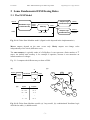
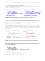
2 Some Fundamental FSM Desing Rules
2.1 The FSM Model
stimuli
NextState Logic
(combinational)
Next
State
Output Logic
(Combinational)
Mealy
Outputs
Output Logic
(Combinational)
Moore
Outputs
state
Memory
state
reset clock
Fig. 2.1-1: Finite-State Machine model. (Signal enable depends in the implementation.)
Moore outputs depend on the state vector only. Mealy outputs can change value
independently of the clock (difficult to test).
The state memory is typically made of n D-flipflops. It can represent a finite number of 2n
states. An infinite state memory is for example a capacitor, because it can memorize an
infinite number of voltages.
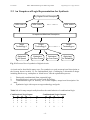
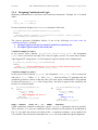
Fig. 2.1-2 compares the different ways to draw a FSM.
(a)
(c)
clk
stimuli
comb.
logic
NextState
memory
state
01
A
D
10
B
reset
00
01
00
(b)
inputs
outputs
0.....0 0
0.....0 1
0.....1 0
0...0
0...1
1...1
...
1.....1 1
E
C
00
10
01
F
11
...
G
0...1
Fig. 2.1-2: Finite-State Machine models (a) Loop model, (b) combinational NextState logic
described as table, (c) bubble model.
-3-
RED / PRED FSM Design for DSP Using VHDL
M. Schubert
Regensburg Univ. of Appl. Sciences
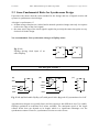
2.2 An Unequivocal Logic Representation for Synthesis
Any Digital Circuit Description
HDL code 1
HDL code 2
HDL code n
Unequivocal Machine Description
Target
Technology 1
Target
Technology 2
Optimized
for Low Power
Optimized
for Speed
Target
Technology m
Optimized
for Low Costs
Optimized
for Reliability
Fig. 2.2: Process flow of synthesis of digital circuits.
A circuit can be described in many ways. For synthesis we need an unequivocal description as
the bit-map shown in table 2.2 for combinational logic. Challenging is hierarchical design
including blocks as e.g. multipliers as “black boxes” into the optimization process.
1.
2.
3.
Distinguish combinational from sequential logic.
Sequential logic is typically realized with D-flipflops.
Combinational logic: no memory, no tri-state outputs; unequivocal description: bitmap.
Synthesize logic with respect to target technology and goals
4.
Table 2.2: A bit map unequivocally describes the static behavior of combinational logic
Combinational Logic Inputs
i1
i2
i3
i4
...
0
0
0
0
...
1
0
0
0
...
1
1
0
0
...
1
1
1
1
...
ix
0
0
0
1
Combinational Logic Outputs
o1 o2 o3 ...
oy
1
0
1
...
0
0
1
1
...
1
1
0
1
...
1
1
-4-
1
0
...
1
RED / PRED FSM Design for DSP Using VHDL
M. Schubert
Regensburg Univ. of Appl. Sciences
2.3 Some Fundamental Rules for Synchronous Design
Experience has shown that the safest method for the design and test of digital circuits and
systems is synchronous circuit design.
A design is synchronous, if
all data storage elements are clocked and in normal operation change state only in response
to the active edge of the clock signal,
the same active edge of the clock signal is applied at precisely the same time point at every
clocked cell in the design.
Not recommended: Non-synchronous changes of flipflop states:
dff
d
Fig. 2.3-1:
Flipflop driving clock input of an
other Flipflop
q
clk
dff
d
q
clk
qb
qb
Do not gate clocks !
(b)
(a)
(c)
data
d
0
q
data
enable
clock
reset
1
mux
dff
dff
d
clk
d
q
e
enable
&
eff
q
clk
clock
r
clk
r
r
reset
Fig. 2.3-2: (a) Bad enable-flipflop (eff) with gated clock, (b) good eff, (c) transistor-level eff.
Asynchronous designs are typically faster and less expensive but difficult to test. Use enableflipflops optimized on transistor-level when available. The maximum speed of the ripple
counter below does not depend on its length, which is a significant advantage over the
synchronous counter. However, synchronous circuits are easier to test.
-5-
RED / PRED FSM Design for DSP Using VHDL
M. Schubert
4-Bit Binary Ripple Counter
tff
clk
q
Regensburg Univ. of Appl. Sciences
4-Bit Synchronous Binary Counter
count_enable
q0
e
clk
clk
etff q
clk
qb
tff
q
qb
&
q1
e
clk
etff q
q
qb
&
q2
e
clk
etff q
q2
clk
qb
tff
q1
clk
qb
tff
q0
q
qb
&
q3
clk
e
etff q
q3
clk
qb
qb
Combinational Logic
Sequential Logic (Memory)
Fig. 2.3-3: (a) asynchronous 4-bit ripple counter, (b) synchronous 4-bit counter.
A toggle flipflop (tff) and an enabled toggle flipflop (etff) uses d=NOT(q).
-6-
M. Schubert
RED / PRED FSM Design for DSP Using VHDL
Regensburg Univ. of Appl. Sciences
3 VHDL Design for Synthesis
3.1 Fundamental Guidelines for Synthesizable VHDL Code
Synthesizable code is typically termed rtl (register transfer level) Code.
Non-synthesizable code is typically termed behavioral (testbenches).
3.1.1
Do not Reinvent the Wheel!
According to Wikipedia [13] "Reinventing the wheel is a phrase that means to duplicate a
basic method that has already previously been created or optimized by others" which
normally doesn’t make sense. In most situations a simple rule delivers the best results:
Describe your circuit as detailed as necessary and as general as possible.
What is synthesizable or not depends on your libraries. An adder or multiplier from
your library is in the majority of cases significantly better than a self-made one.
Do not design primitives at gate level! Particularly flipflops (FFs) are optimized by the
technology foundry. Use behavioral FF descriptions as detailed below.
For information on synthesis exceeding the recommendations below the reader is
referred the literature, in particular to the work of Keating and Bricaud [14], which
results from a joint design-for-reuse initiative of Cadence Systems and Mentor
Graphics.
3.1.2
Design for Portability and Reusability
Preserving portability of VHDL models requires to design without taking advantage of
features offered by particular soft- and hardware manufacturers.
ASYNCHRONOUS RESET: Most FPGAs automatically reset all FFs when they are loaded.
Therefore, some FPGA designers code FFs without reset. However, it is up-to date practice to
test a design in a FPGA before copying the models into an ASIC. When HDL models are
ported to an ASIC, memory without reset will have a problem, as FFs fall randomly into
'0' or '1' state.
Design for reusability is an important topic [14] that would exceed the scope of this tutorial.
-7-
M. Schubert
3.1.3
RED / PRED FSM Design for DSP Using VHDL
Regensburg Univ. of Appl. Sciences
Designing Edge-Triggered Memory
Among the many possibilities of modeling sequential logic VHDL synthesizers are typically
sensitive to the following constructs
a) ps_dff:PROCESS(clk,reset)
BEGIN
IF reset='0' THEN
q<='0' [AFTER delay];
ELSIF clk'EVENT AND clk='1' THEN
q<=d [AFTER delay];
END IF;
END PROCESS ps_dff;
b) ps_state_memory:PROCESS(clk,reset)
BEGIN
IF reset ='0' THEN
state<=reset_state [AFTER delay];
ELSIF clk'EVENT AND clk='1' THEN
state<=next_state [AFTER delay];
END IF;
END PROCESS ps_state_memory;
Listing 3.1.3-1: Modeling memory: (a) for a scalar state and (b) for a state vector.
The AFTER clause is optional, improves simulation and is ignored by the synthesizer. For FFs
with inverting output a model as illustrated in Listing 3.1.3-2(a) is recommended, because it
guarantees qb=NOT(q) in all situations.
Not recommended are constructs assigning both q and qb within the PROCESS statement as
shown in Listing 3.1.3-2(b). During initialization all processes run through and the forbidden
situation q=qb='0' or q=qb='1' may occur, when there is neither a rising clock edge
nor reset='0'.
a) ps_dff_good:PROCESS(clk,reset)
BEGIN
IF reset='0' THEN
q<='0' AFTER delay;
ELSIF clk'EVENT AND clk='1' THEN
q<=d AFTER delay;
END IF;
END PROCESS ps_dff_good;
qb<=NOT(q); -- this is always o.k.
b) ps_dff_err:PROCESS(clk,reset)
BEGIN
IF reset ='0' THEN
q<='0' AFTER delay;
qb<='1' AFTER delay;
ELSIF clk'EVENT AND clk='1' THEN
q<=d AFTER delay;
qb<=NOT(d) AFTER delay;
END IF;
END PROCESS ps_dff_err;
Listing 3.1.3-2: FF model with inverting output: (a) recommended (b) not recommended.
Many silicon foundries offer optimized enable flipflops (EFFs) and the construction shown in
Fig. 2.3-2 can be realized as:
ps_state_memory:PROCESS(clk,reset)
BEGIN
IF reset ='0' THEN
state<=reset_state;
ELSIF clk'EVENT AND clk='1' AND enable='1' THEN
state<=next_state;
END IF;
END PROCESS ps_state_memory;
Listing 3.1.3-3: Design of an enable flipflop (EFF).
-8-
RED / PRED FSM Design for DSP Using VHDL
M. Schubert
3.1.4
Regensburg Univ. of Appl. Sciences
Designing Combinational Logic
Modeling combinational is well done with concurrent statements. Example for a 1-bit half
adder:
sum
<= a xor b;
carry_out <= a AND b;
In many situations designers use a PROCESS statement of the form
ps_combinational:PROCESS(sensitive_signals)
BEGIN
driven_output_signals <= f(sensitive_signals, other_signals);
END PROCESS ps_combinational;
The process generates (forbidden) latches, if one of the following two basic rules for
combinational logic is violated:
1. All input signals of the process must be listed in its sensitivity list.
2. All output signals must be driven all time.
Violation example for rule 1:
In the process below labeled ps_partial_sensitivity_list the assignment
y<=b; can be executed if and only if an event on signal a occurs. To realize that a doubleedge triggered FF using signal a as clock signal is required, which is not combinational.
ps_partial_sensitivity_list:PROCESS(a)
BEGIN
y<=b; -- latch generation: b is not in the sesitivity list!
END PROCESS ps_partial_sensitivity_list;
Violation example for rule 2:
In the process below labeled ps_wrong the assignment next_y<=b; can be executed if
and only if a='1'. When a='0' then next_y must not change. To guarantee this the
synthesizer generates a latch, so that the code is no more purely combinational. This problem
is removed in process ps_good. Don’t forget that y has now to appear in the sensitivity list
because it is an input signal.
a)
b)
ps_wrong:PROCESS(a,b)
BEGIN
IF a='1' THEN
next_y <= b;
-- what happens if a='0'?
END IF;
END PROCESS ps_wrong;
ps_good:PROCESS(a,b,y)
BEGIN
IF a='1' THEN
next_y <= b;
ELSE
next_y <= y;
END IF;
END PROCESS ps_good;
versus IF | "<= … WHEN" statement.
VHDL synthesizer manuals recommend to prefer CASE to IF statements wherever possible.
This is because CASE uses one conditions for the evaluation of all situations as symbolized in
Fig. 3.3.1(a) while the priority bit coding of the IF statement evaluates a new condition for
every branch. The concurrent counterparts are SELECTed and conditional signal assignment.
CASE | SELECT
-9-
RED / PRED FSM Design for DSP Using VHDL
M. Schubert
(a)
Regensburg Univ. of Appl. Sciences
(b)
in0
in1
in2
in3
in4
in5
in6
in7
y_sel
in0
in1
in2
in3
in4
in5
in6
in7
condition
y_cond
condition 1
condition 2
condition 3
condition 4
condition 5
condition 6
condition 7
Fig. 3.1.4: Conditional VHDL assignments (a) using the sequential CASE <condition> IS
or concurrent WITH <condition> SELECT statement, (b) using the sequential IF
<condition>
THEN
or
concurrent
<signal> <= <expression>
WHEN<condition> statement
End conditional statements with an OTHERS or ELSE clause. Be aware of state values
other than '0' and '1', e.g. logic 'X'. Even if it is sure at the moment that all cases are
covered by a CASE statement, the designer should keep in mind that the code may be
maintained or reused by other persons. (Exceptions to this rule hold for FSM design using
ONE process for next-state logic and memory -> see below.)
Examples: Let us assume the following VHDL signal declaration:
SIGNAL condition,a,b,y:std_logic ;
Selected signal assignment:
Concurrent
WITH condition
y <= a WHEN
b WHEN
'X' WHEN
SELECT
'0',
'1',
OTHERS;
Conditional signal assignment:
Concurrent:
y <=
a WHEN condition='0'
ELSE b WHEN condition='1'
ELSE 'X';
Sequential
p_case: PROCESS(condition,a,b)
BEGIN
CASE condition IS
WHEN '0'
=> y<=a;
WHEN '1'
=> y<=b;
WHEN OTHERS => y<='X';
END CASE
END PROCESS p_case;
Sequential
p_if: PROCESS(condition,a,b)
BEGIN
IF condition='0'
THEN y<=a;
ELSIF condition='1' THEN y<=b;
ELSE
y<='X';
END IF
END PROCESS p_if;
- 10 -
M. Schubert
RED / PRED FSM Design for DSP Using VHDL
Regensburg Univ. of Appl. Sciences
3.2 VHDL-Design of Synchronous Finite State Machines
3.2.1
General Guidelines for Event-Driven FSM Design
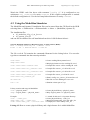
stimuli
Output Logic
Mealy
clock
G(Stimuli,State)
outputs
stimuli
Next State Logic
State
Memory
NextState
Moore
state
F(Stimuli,State)
state
enable
outputs
Output Logic
synchronous_reset
asynchronous_reset
Moore
H(State)
State
Fig. 3.2.1-1: Clocked state machine structure: Mealy/Moore machine. Moore outputs depend
only on state and not on stimuli, the latter may be asynchronous. Signal enable depends on
the implementation (can be avoided by not changing NextState).
Avoid Mealy outputs if possible. Mealy outputs depend directly on input signals and are
difficult to test because they are subject to change any time. The delay of a chain of modules
with mealy outputs is difficult to predict.
There are two possibilities to code the feedback-loop of a finite state machine:
1. Using a single process for both next-state logic and memory.
2. Using two processes: one for the next-state logic and an other for the memory.
Example counter: We will now build the counter known from the Matlab model above.
counter
Fig. 3.2.1-2: The counter entity corresponds
to the schematics symbol. The prefix 'c'
denotes cPeriod as a constant (Constants
are passed to a VHDL entity as "generics".)
cPeriod
cM
count
enable
maxflg
clock
reset
A bitwidth cM can be declared directly using e.g. std_logic_vector(cM-1 DOWNTO 0)
or INTEGER RANGE 0 TO 2**cM, or indirectly using e.g. INTEGER RANGE 0 TO 2**cM.
In
this
case
the
bitwidth
can
be
computed
from
the
C-code
- 11 -
RED / PRED FSM Design for DSP Using VHDL
M. Schubert
Regensburg Univ. of Appl. Sciences
cM=(int)ceil(log(cMax)/log(2)), where the logarithms dualis can be computed from
ld(x)=loga(x)/loga(2) for any base a.
Entity: Assume the following Entity for the counter that counts from 0...cPeriod-1.
ENTITY counter IS
GENERIC(cPeriod:POSITIVE:=10);
PORT(reset,clock,enable:IN std_logic;
maxflg:BUFFER std_logic;
count:BUFFER NATURAL RANGE 0 TO cPeriod-1
);
END ENTITY counter;
There are two design techniques to model the feedback-loop a FSM: Two PROCESS
statements for next-state logic and memory or a single PROCESS statement for both.
3.2.2
Two
PROCESS
Statements for Next-State Logic and State Memory
ARCHITECTURE rtl_counter2 OF counter IS
SIGNAL NextCount:NATURAL RANGE 0 TO cPeriod-1;
BEGIN
-- Begin NextState Logic:
p_ns:PROCESS(enable,count) BEGIN
IF enable='1' THEN
IF count = cPeriod-1 THEN
NextCount<=0;
ELSE
NextCount<=count+1;
END IF;
ELSE
-- what happens at enable ='0' ?!
NextCount<=count;
END IF;
END PROCESS; -- End NextState Logic
--- Begin State Memory
p_mem:PROCESS(reset,clock)
BEGIN
IF reset='0' THEN
count <= 0;
ELSIF clock'EVENT AND clock='1' THEN
count <= NextCount;
END IF;
END PROCESS p_mem;
--- output logic:
maxflg <= '1' WHEN count=cPeriod-1 ELSE '0';
END ARCHITECTURE rtl_counter2;
CONFIGURATION con_counter2 OF counter IS
FOR rtl_counter2
END FOR;
END CONFIGURATION con_counter2;
- 12 -
RED / PRED FSM Design for DSP Using VHDL
M. Schubert
Regensburg Univ. of Appl. Sciences
The above example reflects the state machine composed of next-state logic and memory.
When choosing this solution, you should keep in mind the 2 rules for combinational logic:
1. Have all input signals in the sensitivity list of the combinational-logic process and
2. Drive every output-bit of the next-state logic any time in any situation. (Use ELSE and
OTHERS keywords in IF and CASE statements, respectively!)
One method to guarantee point two above is to begin the combinational next-state process
with the following code line:
State <= NextState;
Within a process the last of several signal assignments is valid. So we have driven any bit of
the state vector and may now drive some of its bits if desired.
3.2.3
One
PROCESS
Statement for Next-State Logic and State Memory
ARCHITECTURE rtl_counter1 OF counter IS
SIGNAL NextCount:NATURAL RANGE 0 TO cPeriod-1;
BEGIN
-- Counter
p_fsm:PROCESS(reset,clock)
BEGIN
IF reset='0' THEN
count <= 0;
ELSIF clock'EVENT AND clock='1' AND enable='1' THEN
IF count = cPeriod-1 THEN -- Begin NextState Logic
count <= 0;
ELSE
count <= count+1;
END IF;
-- End NextState Logic
END IF;
END PROCESS p_fsm;
--- output logic:
maxflg <= '1' WHEN count=cPeriod-1 ELSE '0';
END ARCHITECTURE rtl_counter1;
This realization uses the same memory model as the example above, but replaces the nextstate assignment count<=NextCount; by the combinational logic. Advantages:
There are no other signals in the sensitivity list than reset and clock,
There is no ELSE or OTHERS clause to define what happens when enable='0',
Such code is often easier to read, shorter and less error prone to maintain.
To obtain the solution in example 2 from the solution in example 1 …
1. Replace the statement count<=NextCount; (or state<=NextState;) inside the
memory by the next-state logic.
2. Rename NextCount to count (or NextState to state) and remove the signal
declaration statement for the NextCount (or NextState) vector.
3. Remove the process for the NextState logic.
- 13 -
M. Schubert
RED / PRED FSM Design for DSP Using VHDL
Regensburg Univ. of Appl. Sciences
4 Simulate the VHDL Model
4.1 VHDL Testbench
LIBRARY ieee; USE ieee.std_logic_1164.ALL;
ENTITY tb_counter IS END ENTITY tb_counter;
LIBRARY ieee;
USE ieee.std_logic_1164.ALL;
ARCHITECTURE beh_tb_counter OF tb_counter IS
CONSTANT cPeriod:NATURAL:=10;
SIGNAL count:NATURAL RANGE 0 TO cPeriod-1;
SIGNAL reset,clock,maxflg:std_logic:='0';
SIGNAL enable:std_logic;
-COMPONENT counter IS
GENERIC(cPeriod:POSITIVE:=10);
PORT(reset,clock,enable:IN std_logic;
maxflg:BUFFER std_logic;
count:BUFFER NATURAL RANGE 0 TO cPeriod-1
);
END COMPONENT counter;
CONSTANT fclk:REAL:=50.0E6;
BEGIN
clock <= NOT clock AFTER sec/(2.0*fclk);
reset <= '0', '1' AFTER 12 ns;
enable <= '1', '0' AFTER 355 ns, '1' AFTER 545 ns;
i:counter GENERIC MAP(cPeriod)
PORT MAP(reset,clock,enable,maxflg,count);
END ARCHITECTURE beh_tb_counter;
CONFIGURATION con_tb_counter OF tb_counter IS
FOR beh_tb_counter
FOR i:counter USE ENTITY WORK.counter(rtl_counter2); -- config #
END FOR;
END FOR;
END CONFIGURATION con_tb_counter;
Fig. 4.1: Simulation of the code above obtained with the ModelSim simulator
- 14 -
M. Schubert
RED / PRED FSM Design for DSP Using VHDL
Regensburg Univ. of Appl. Sciences
Watch the VHDL code line above with comment "config #". It is configured to use
architecture rtl_counter2 for entity counter. If this explicit configuration is omitted
the default configuration is: Use the last compiled architecture for entity counter.
4.2 Using the ModelSim Simulator
The ModelSim and Quartus II installation files can be started from the CIP-Pools in the HS.R
selecting Start Fachbereiche Elektrotechnik Altera {ModelSim | Quartus II}.
The installation files
81_modelsim_6.3g_p1_ae_free.exe
81_quartus_free.exe
and can also be obtained for self-installation from drive k:\Sb\Software\Altera\...
Start the ModelSim simulator at Regensburg Univ. of Appl. Sciences (HS.R):
File -> Change Directory -> …\counter -> ok
Tools -> Tcl -> Execute Macro -> work.do
The file work.do Tcl-contains the commands illustrated in the listing below. You can also
type these commands into the transcript window.
vlib work
# Create working library named work
vmap work work
# Map logical name work to working lib. work
vcom -work work counter.vhd
# Compile file counter.vhd to working lib. work
vcom -work work rtl_ounter1.vhd
# Compile file counter1_rtl.vhd to lib. work
vcom -work work rtl_counter2.vhd
# Compile file counter2_rtl.vhd to lib. work
vcom -work work counter_tb.vhd
# Compile file counter_tb.vhd to lib. work
vsim work.con_counter_tb
# Simul. config. con_counter_tb located in work
do wave.do
# Run file wave.do defining the wave-win
run 1 us
# Simulate a time span of 1 μs
Library creation and usage in ModelSim:
vlib <physical_name>
vmap <logical_name> <physical_name>
# Create physical library <physical_name>
# Map <logical_name> to <physical_name>
Example:
vlib ../adac_bin
vmap adac_lib ../adac_bin
vcom -work adac_lib ../filter.vhd
# '.' stands for this and '..' for parent directory:
# Create physical library ../adac_bin
# Map logical name adac_lib to lib. adac_bin
# Compile filter.vhd to library adac_lib
Listing 4.2: How to create a physical library and a logical name for it within ModelSim
- 15 -
M. Schubert
RED / PRED FSM Design for DSP Using VHDL
Regensburg Univ. of Appl. Sciences
Exercise: Writing VHDL Code
Take the architecture listings rtl_counter# (#=1,2) above. Delete some of the code lines
describing the FSM as shown below. Rewrite the model by yourself and test it.
ARCHITECTURE rtl_counter2 OF counter IS
SIGNAL NextCount:NATURAL RANGE 0 TO cPeriod-1;
BEGIN
-- Begin NextState Logic:
p_ns:PROCESS(.....................) BEGIN
..............................................................
..............................................................
..............................................................
..............................................................
..............................................................
..............................................................
..............................................................
..............................................................
..............................................................
..............................................................
END PROCESS; -- End NextState Logic
--- Begin State Memory
p_mem:PROCESS(.....................)
BEGIN
IF reset='0' THEN
count <= 0;
ELSIF clock'EVENT AND clock='1' THEN
..............................................................
END IF;
END PROCESS p_mem;
--- output logic:
maxflg <= '1' WHEN count=cPeriod-1 ELSE '0';
END ARCHITECTURE rtl_counter2;
- 16 -
M. Schubert
RED / PRED FSM Design for DSP Using VHDL
Regensburg Univ. of Appl. Sciences
ARCHITECTURE rtl_counter1 OF counter IS
SIGNAL NextCount:NATURAL RANGE 0 TO cPeriod-1;
BEGIN
-- Counter
p_fsm:PROCESS(
)
BEGIN
IF reset='0' THEN
count <= 0;
ELSIF clock'EVENT AND clock='1'........................... THEN
-- begin encapsulated combinational Next-State logic:
-- end of encapsulated combinational Next-State logic
END IF;
END PROCESS p_fsm;
--- output logic:
maxflg <= '1' WHEN count=cPeriod-1 ELSE '0';
END ARCHITECTURE rtl_counter1;
Hint: You will find the solution in “ARCHITECTURE rtl_counter# OF counter“ above (#=1,2).
- 17 -
M. Schubert
RED / PRED FSM Design for DSP Using VHDL
Regensburg Univ. of Appl. Sciences
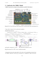
5 Synthesize the VHDL Model
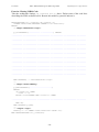
VHDL Testbench for Synthesis & Download into the DE2 FPGA Board
Fig. 5.1: The Terasic DE2 board with Altera FPGA, copied from the DE2 User Manual [12].
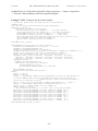
Using Altera’s Quartus II [6] to perform the synthesis
Start Quartus II version 8.1
Create a New Project -> Next ->
Directory: "…\counter", Files "counter.vhd" + "counter1_rtl.vhd"
Project: de2_counter, top-level design entity: de2_counter -> Finish
Project -> Add/Remove Files in Project -> (add all required files)
Assignments -> Import Assignments -> DE2_pin_assignments.csv -> Open, ok
Processing -> Start Compilation
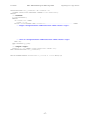
Tools -> Netlist -> RTL Viewer (creates Fig. 3.3.6)
Tools -> Programmer [1st use only: -> Hardware Setup -> USB-Blaster [USB-0] ]
(a) Interface compent de2_counter
(b) Synthesized component counter
Fig. 5.2: Quartus II 8.1 RTL Viewer: synthesized models
Assignments between the port signals of the entity and corresponding on-board wires
are defined within the file DE2_pin_assignments.csv supplied by Altera and can be
- 18 -
M. Schubert
RED / PRED FSM Design for DSP Using VHDL
Regensburg Univ. of Appl. Sciences
modified there. It is imported to Quartus2 using Assignments → Import Assignments...
→ Filename. Short summary of the most important signals.
Listing 5: VHDL Testbench for the counter module
-- For Board: Altera DE2 with FPGA cyclone II EP2C35F672C6
LIBRARY ieee;
USE ieee.std_logic_1164.ALL,ieee.std_logic_signed.ALL;
ENTITY de2_counter IS
PORT(CLOCK_50,CLOCK_27:IN std_logic;
key:IN std_logic_vector(3 DOWNTO 0); -- low when pressed
sw:IN std_logic_vector(17 DOWNTO 0); -- low when pulled down
ledg:BUFFER std_logic_vector(8 DOWNTO 0); -- high active
ledr:BUFFER std_logic_vector(17 DOWNTO 0); -- high active
hex0,hex1,hex2,hex3,hex4,hex5,hex6,hex7:OUT std_logic_vector(0 TO 6);
gpio_0:BUFFER std_logic_vector(35 DOWNTO 0);
gpio_1:INOUT std_logic_vector(35 DOWNTO 0)
);
END ENTITY de2_counter;
ARCHITECTURE rtl_de2_counter OF de2_counter IS
CONSTANT cPeriod:NATURAL:=2_147_483_647; -- 2**31-1
CONSTANT cCountWidth:NATURAL:=32;
SIGNAL count:NATURAL RANGE 0 TO cPeriod-1;
CONSTANT cZeroVector:std_logic_vector(cCountWidth-1 DOWNTO 0):=(OTHERS=>'0');
SIGNAL count_vector:std_logic_vector(cCountWidth-1 DOWNTO 0);
TYPE t_7seg IS ARRAY(0 TO 15) OF std_logic_vector(0 TO 6);
CONSTANT c7seg:t_7seg:=("1111110", "0110000", "1101101", "1111001",
"0110011", "1011011", "1011111", "1110000", "1111111", "1110011",
"1110111", "0011111", "1001110", "0111101", "1001111", "1000111");
COMPONENT counter IS
GENERIC(cPeriod:POSITIVE:=10);
PORT(reset,clock,enable:IN std_logic;
maxflg:BUFFER std_logic;
count:BUFFER NATURAL RANGE 0 TO cPeriod-1
);
END COMPONENT counter;
SIGNAL reset,enable,maxflg:std_logic;
BEGIN
reset <= key(0);
enable <= key(1);
ledg(6) <= NOT ledg(6) WHEN clock_50'EVENT AND clock_50='1' AND maxflg='1';
i:counter GENERIC MAP(cPeriod) PORT MAP(reset=>key(0),clock=>clock_50,
enable=>key(1),count=>count,maxflg=>maxflg);
count_vector<=cZeroVector+count;
ledr <= count_vector(cCountWidth-2 DOWNTO cCountWidth-19); -- MSB='0'
ledg(8) <= NOT ledg(8) WHEN ledr(11)'EVENT AND ledr(11)='1';
ledg(7)<=sw(7); ledg(5 DOWNTO 4)<=sw(5 DOWNTO 4);
ledg(3 DOWNTO 0) <= key;
-- use concatenated leading '0' as data type is std_logic_signed:
hex7<=NOT c7seg(CONV_INTEGER('0'&count_vector(31 DOWNTO 28)));
hex6<=NOT c7seg(CONV_INTEGER('0'&count_vector(27 DOWNTO 24)));
hex5<=NOT c7seg(CONV_INTEGER('0'&count_vector(23 DOWNTO 20)));
hex4<=NOT c7seg(CONV_INTEGER('0'&count_vector(19 DOWNTO 16)));
hex3<=NOT c7seg(CONV_INTEGER('0'&count_vector(15 DOWNTO 12)));
hex2<=NOT c7seg(CONV_INTEGER('0'&count_vector(11 DOWNTO 8)));
hex1<=NOT c7seg(CONV_INTEGER('0'&count_vector( 7 DOWNTO 4)));
hex0<=NOT c7seg(CONV_INTEGER('0'&count_vector( 3 DOWNTO 0)));
END ARCHITECTURE rtl_de2_counter;
- 19 -
M. Schubert
RED / PRED FSM Design for DSP Using VHDL
Regensburg Univ. of Appl. Sciences
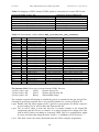
Table 5.1: Mapping of FPGA-internal VHDL signals to external devices on the DE2 board
Signal in the PORT of entity de2_...
CLOCK_50,CLOCK_27:IN std_logic
key:IN std_logic_vector(3 DOWNTO 0);
sw:IN std_logic_vector(17 DOWNTO 0);
ledg:BUFFER std_logic_vector(7 DOWNTO 0);
ledr:BUFFER std_logic_vector(17 DOWNTO 0);
hex0,hex1,hex2,hex3,hex4,hex5,hex6,hex7
Connected to element of DE2 board
External 50MHz and 27MHz clocks
the 4 push buttons below green diodes
low when pulled down
Green LEDs, high active
Red LEDs, high active
7-segment displays, low-active
Table 5.2: Functionality of the testbench de2_counter(rtl_de2_counter):
Signal name mode
key(0)
IN
key(1)
IN
key(2)
IN
key(3)
IN
sw(17:0)
IN
ledg(0)
OUT
ledg(1)
OUT
ledg(2)
OUT
ledg(3)
OUT
ledg(4)
OUT
ledg(5)
OUT
ledg(6)
OUT
ledg(7)
OUT
ledg(8)
OUT
ledr(17:0)
OUT
hex7
OUT
hex7
OUT
hex7
OUT
hex7
OUT
hex7
OUT
hex7
OUT
hex7
OUT
hex7
OUT
features
'0' when key pressed
'0' when key pressed
'0' when key pressed
'0' when key pressed
'1' when pushed to board
LED is on @ '1'
LED is on @ '1'
LED is on @ '1'
LED is on @ '1'
LED is on @ '1'
LED is on @ '1'
LED is on @ '1'
LED is on @ '1'
LED is on @ '1'
LED is on @ '1'
LEDs on @ '0'
LEDs on @ '0'
LEDs on @ '0'
LEDs on @ '0'
LEDs on @ '0'
LEDs on @ '0'
LEDs on @ '0'
LEDs on @ '0'
functionality
reset
enable for counter
= key(0)= reset
= key(1)= enable
= key(2)
= key(3)
= sw(4)
= sw(5)
NOT ledg(6) @ maxflg
= sw(7)
toggles with ledr(11)
=count_vector(31:13)
=>count_vector(31:28)
=>count_vector(27:24)
=>count_vector(23:20)
=>count_vector(19:16)
=>count_vector(15:12)
=>count_vector(11:08)
=>count_vector(07:04)
=>count_vector(03:00)
comments
resets all components when pressed
toggles when maxflg='1'
should flash with ca. 1Hz
makes toggling msb’s visible
makes counter content visible
makes counter content visible
makes counter content visible
makes counter content visible
makes counter content visible
makes counter content visible
makes counter content visible
makes counter content visible
The Quartus II 8.1 files to save (except from the VHDL files) are
<project_name>.qpf
ASCII
Quartus Project file
<project_name>.qsf
ASCII
Quartus Specification file
<project_name>.sof
Binary
downloadable image
The complete required information to rebuild the project is contained in the qpf and qsf files.
(Linking of previously compiled files is not possible with the free version of Quartus II.)
.qpf: Double-click left mouse button on the *.qpf file to open Quartus II with the respective
project loaded. Use an ASCII editor and look into this file.
.qsf: Use an ASCII editor to look into this file: It contains settings as the Signal–Pin
assignments and the files are to compile. It is always dangerous to change such files
with an ASCII editor, but adding or removing VHDL files to be compiled here might
be easier and faster than using the menu “Project Add/Remove File in Project...”.
.sof: This final "result" file can be downloaded into the FPGA using the programmer.
- 20 -
RED / PRED FSM Design for DSP Using VHDL
M. Schubert
Regensburg Univ. of Appl. Sciences
6 VHDL
This chapter points out some important issues of VHDL, it is no comprehensive tutorial. It is
based on the author’s experience of frequently asked questions during circuit design courses
with students having some previous knowledge on that topic.
6.1 Design Units
Table 6.1: Building blocks in VHDL
To the outer world
Realization inside
Combination
COMPONENT
LIBRARY
Comments
ENTITY
PACKAGE
Corresponds to a symbol
ARCITECTURE
BPACKAGE BODY Corresponds to a schematics
CONFIGURATION
6.2 Compilation Order Dependence
VHDL is compilation order dependent. It has no linker but only a loader. Sub-modules are
loaded immediately during the compilation process. We can organize our VHDL code
arbitrarily in different files, but it is important that code which is used by other code is
compiled before the code using it. The compilation sequence is
PACKAGE ENTITY ARCHITECTURE PACKAGE BODY
The package body may be compiled directly after the package but also as lastly.
6.3 Kinds of Code: Concurrent – Sequential – Structural
VHDL code can be written in three different modes: Concurrent is the default mode. In
concurrent code the sequence of statements is irrelevant. Using components is structural and
within a PROCESS statement or subprograms code is sequential, i.e. it is processed top-down.
6.4 Data
6.4.1
Data Objects
VHDL handles data by one of the following data objects:
1.SIGNAL:
2.VARIABLE:
3.CONSTANT:
interconnection wires
local storage of temporary data
named constant values
Table 6.4.1 shows in which environment a data object may be declared and where it may be
used, i.e. assigned or read.
- 21 -
RED / PRED FSM Design for DSP Using VHDL
M. Schubert
Regensburg Univ. of Appl. Sciences
Table 6.1: The three data objects and the environments where they may be declared and used.
data object
SIGNAL
VARIABLE
CONSTANT
environment to be declared in
concurrent
sequential
everywhere
environment to be used in
everywhere
sequential
everywhere
Objecs
_______________________|_______________________
|
|
|
SIGNAL
VARIABLE
CONSTANT
Fig. 6.4.1: VHDL data objects.
6.4.2
Data Types
Data object have to be declared with a data type. Available are scalar the types INTEGER,
REAL, enumerated and BIT and the composite data types such ARRAY and RECORD.
Scheme of data type declaration statements:
TYPE type_name IS type_mark;
SUBTYPE subtype_name IS <range_specification> OF type_name;
Examples for type and subtype declarations:
TYPE BOOLEAN IS (false,true);
SUBTYPE t_address IS RANGE 0 TO 15 OF INTEGER;
SUBTYPE NATURAL IS RANGE 0 TO INTEGER'HIGH OF INTEGER;
Types
|
_____________________|_______________________
|
|
|
|
Access
Scalar
File
Composite
|
|
___|___
_____________|_____________
|
|
|
|
|
|
Integer Real
Physical Enumerated
Array Record
Fig. 6.4.2: VHDL data types.
The assignment of a value to a data object is guarded such, that only values of the same data
type or a subtype can be assigned to a data object. The user can specifiy own data types. See
e.g. [Schubert: VHDL Skript] Chapter 2: Data for more details.
- 22 -
M. Schubert
RED / PRED FSM Design for DSP Using VHDL
Regensburg Univ. of Appl. Sciences
6.5 Libraries and Packages
6.5.1
Using Existing Libraries and Packages
Reinventing the wheel is inefficient. Better reuse existing code if possible. It is typically
organized in libraries which are composed of packages. A typical library retrieval is
(1)
(2)
(3)
(4)
(5)
(6)
LIBRARY ieee;
USE ieee.std_logic_1164.ALL;
USE ieee.std_logic_unsigned."+";
LIBRARY adac_lib;
USE adac_lib.pk_adac.ALL;
USE work.pk_mypack.ALL;
The code above has the following meanings:
Line (1): "Retrieve library with name ieee".
Line (2): Use ALL from package std_logic_1164 found within library ieee.
Line (3): Use only the declaration of the "+" operator found in package
std_logic_unsigned within library ieee. Applied on bit-vectors as
operands it will be synthesized as arithmetic summation and the most significant
bit will not be interpreted as sign bit. (To treat the first bit as sign bit use the "+"
operator from package std_logic_signed.)
Line (4): "Retrieve library with name adac_lib". As it is not a standard library it must be
introduced to the tool, the respective commands are tool dependent.
Line (5): Use ALL declarations from package pk_adac found within library adac_lib.
Line (6): Use ALL declarations from package pk_mypack found within library work.
The working library work needs no LIBRARY statement, at is always linked.
If the LIBRARY / USE statements are written above ...
an ENTITY, then they are valid for this entity and its architectures,
an ARCHITECTURE, then they are valid for this architecture,
a PACKAGE, then they are valid for this package and its package body,
a PACKAGE BODY, then they are valid for this PACKAGE BODY.
6.5.2
Creating an Own Package
Package and package body are like entity and architecture. Packages may contain nonexecutable declarations only while package bodies may contain executable code also.
Declarations made within a package are available whenever loading this package.
Declarations made in a package body are known only in this package body below the
declaration. Listing 4.2 shows Tcl-commands to create a library and symbol for it that can be
used within the VHDL code when working with the ModelSim simulator.
- 23 -
M. Schubert
RED / PRED FSM Design for DSP Using VHDL
Regensburg Univ. of Appl. Sciences
LIBRARY ieee; USE ieee.std_logic_1164.ALL;
PACKAGE pk_example IS
-- Declaration of an externally visible constant:
CONSTANT cExtern:INTEGER:=10;
--- gate delay as "deferred" constant: no value assigned:
CONSTANT delay:TIME;
--- multiplexer: interface declaration only, no executable code:
FUNCTION mux(sel:INTEGER;vec:std_logic_vector) RETURN std_logic;
-SIGNAL big_array:std_logic_vector(1 TO 40_000);
END PACKAGE pk_example;
PACKAGE BODY pk_example IS
-- Declaration of an only internally visible constant:
CONSTANT cIntern:INTEGER:=20;
--- here the deferred constant has to get its value:
CONSTANT delay:TIME:=2 ns;
--- here the function mux has to get its body:
FUNCTION mux(sel:INTEGER;vec:std_logic_vector) RETURN std_logic IS
BEGIN
RETURN vec(sel);
END FUNCTION mux;
END PACKAGE BODY pk_example;
The package named pk_example above declares the constant cExtern. It will be
available in the package body and everywhere where this package is declared. This is
different from the constant cIntern declared within the package body below. It will be
known only within this package body and below its declaration.
The constant delay is a so-called deferred constant, as no value is assigned to it in the
package. The assignment is deferred (Latin: carried away) into the package body. As the
package body may be compiled as last design unit, different delays (e.g. for fast, typical, slow
parameters) can be passed to the design by compiling nothing else than the package body.
The external interface of the multiplexer function mux is declared in the package. In the
package body function mux gets its executable body. If the declaration in the package is
omitted, this function will be known only in the package body and after its declaration.
Signal big_array will be declared in any design unit where package pk_example is
declared. It will be different signals which are independent from each other in any of those
design units.
- 24 -
RED / PRED FSM Design for DSP Using VHDL
M. Schubert
Regensburg Univ. of Appl. Sciences
6.6 Arrays for State-Machine Design
filter_canon2
a1
a2
a3
xi ,
X(z)
ns1
z-1
s1 ns2
z-1
s2
ns3
z-1
s3
nsc
z-1
sc
ac
yi, Y(z)
(a) Digital Filter in 2nd canonical direct structure, ai, si and nsi (i=1...c) are bit-vectors.
t_coef :
t_state :
t_CoefVector :
t_StateVector :
t_state
t_coef
(b) Data structures to realize the vectors of coefficients (ai) and data words (si, nsi).
Fig. 6.6: (a) A model that requires a vector of bit-vectors and (b) a VHDL realization.
Fig. 6.6(a) illustrates a digital filter that requires vectors of bit-vectors. Fig. 6.6 (b) and
listing 6.6 realize a single coefficient ai alias CoefVector(i) as bit-vector of type
t_coef. All coefficients are summarized in the constant CoefVector of type
t_CoefVector. A single state or next-state is realized as bit-vector of data type t_state.
A vector of such signals, e.g. named state or NextState, can be declared as signal of
type t_StateVector.
- 25 -
M. Schubert
RED / PRED FSM Design for DSP Using VHDL
Regensburg Univ. of Appl. Sciences
Listing 6.6 (a): The package pk_filter.
(Note: Some synthesizers cannot assign the values of "deferred constant" CoefVector in the package body. In this case
remove the package body and assign the values in the package. Doing so you loose the capability of changing filter
coefficients by recompiling the package bode only, you have to recompile the entire design.)
(1)
(2)
(3)
(4)
(5)
(6)
(7)
(8)
(9)
(10)
(11)
(12)
(13)
(14)
(15)
(16)
(17)
(18)
(19)
(20)
(21)
----------------------------------------------------------------------- Module
: pk_filter
-- Designer
: Martin Schubert
-- Date last modified: 07.03.2011
-- Purpose
: Data Structures for Digital FIR Filter
---------------------------------------------------------------------LIBRARY ieee; USE ieee.std_logic_1164.ALL;
PACKAGE pk_filter IS
CONSTANT cDataInWidth:POSITIVE:=18; -- Input-Data BitWidth
CONSTANT cDataInFract:POSITIVE:=16; -- No of Input-Data fract. Bits
CONSTANT cDataOutWidth:POSITIVE:=18; -- Output-Data BitWidth
CONSTANT cDataOutFract:POSITIVE:=16; -- No of Output-Data fract Bits
CONSTANT cCoefWidth:POSITIVE:=18;
-- Coefficient's BitWidth
CONSTANT cCoefFract:POSITIVE:=18;
-- No of Coef's fractional Bits
SUBTYPE t_DataIn IS std_logic_vector(cDataInWidth-1 DOWNTO 0);
SUBTYPE t_DataOut IS std_logic_vector(cDataOutWidth-1 DOWNTO 0);
SUBTYPE t_coef IS std_logic_vector(cCoefWidth-1 DOWNTO 0);
TYPE
t_CoefVector IS ARRAY(NATURAL RANGE <>) OF t_coef;
CONSTANT cTaps:POSITIVE:=33;
CONSTANT CoefVector: t_CoefVector(1 TO cTaps);
END PACKAGE pk_filter;
Listing 6.6 (b): The package body pk_filter.
(22) PACKAGE BODY pk_filter IS
(23)
CONSTANT CoefVector: t_CoefVector(1 TO cTaps)
(24)
:= (OTHERS=>(cCoefWidth-6=>'1',OTHERS=>'0'));
(25) END PACKAGE BODY pk_filter;
6.7 Exercise: (Solutions at the end of this sub-chapter)
(=16P)
Complete package pk_filter in listing 6.7.
Make sure that data type std_logic and vectors with elements of this type can be used
according to the respective IEEE standard.
(2P)
Complete line (10) such, that data type t_DataIn declares a vector representing a number
with cDataInWidth bits of type std_logic .
(1P)
Complete line (11) such, that data type t_coef declares a vector representing a number
with cCoefWidth bits of type std_logic .
(1P)
Complete line (12) such, that data type t_CoefVector declares a vector with elements
type t_coef . The index range of this vector can be defined later with natural numbers.
(2P)
No value is assigned to the constant in line (14). Where does this constant gets its value and
what is the correct denomination of such a constant?
(2P)
..................................................................
- 26 -
RED / PRED FSM Design for DSP Using VHDL
M. Schubert
Regensburg Univ. of Appl. Sciences
What do you write over an Entity to make all declarations in Package pk_filter available?
..................................................................
Listing 6.7: Package pk_filter.
(1)
....................................................................
(2)
....................................................................
(3)
PACKAGE pk_filter IS
(4)
CONSTANT cDataInWidth:POSITIVE:=8;
-- Input-Data BitWidth
(5)
CONSTANT cDataInFract:POSITIVE:=6;
-- No of Input-Data fract. Bits
(6)
CONSTANT cDataOutWidth:POSITIVE:=18; -- Output-Data BitWidth
(7)
CONSTANT cDataOutFract:POSITIVE:=16; -- No of Output-Data fract Bits
(8)
CONSTANT cCoefWidth:POSITIVE:=18;
-- Coefficient's BitWidth
(9)
CONSTANT cCoefFract:POSITIVE:=18;
-- No of Coef's fractional Bits
(10)
...TYPE
t_DataIn
IS .............................................
(11)
...TYPE
t_coef
IS .............................................
(12)
...TYPE
t_CoefVector IS ..........................................
(13)
CONSTANT cTaps:POSITIVE:=33;
(14)
CONSTANT CoefVector: t_CoefVector(1 TO cTaps);
(15) END PACKAGE pk_filter;
- 27 -
(2P)
M. Schubert
RED / PRED FSM Design for DSP Using VHDL
Regensburg Univ. of Appl. Sciences
Write a library statement at (16), that allows for the multiplication of numbers in the
std_logic_vector-format using '*' (while library is known).
(1P)
Line (17): Declaration of type t_product as funktion of constants such, that a signal of
that type matches the product of t_DataIn and t_coef type signals.
(1P)
Line (18): declaration of signal product such, that we can write the VHDL command:
"product<=DataIn*CoefVector(i);"
(2P)
Lines (20) and (21): Complete the declarations of iPl und iPh such, that (22) works
respecting the vector lengths and the number of fractional bits using the respective named
constants in package pk_filter. (For the computation of iPl, iPh see document “FSM
Design for DSP Using Fixed-Point Numbers” [10]).
(2P)
(16) ....................................................................
(17) ....................................................................
(18) ....................................................................
(19) SIGNAL DataOut:t_DataOut;
(20) CONSTANT iPl: ......................................................
(21) CONSTANT iPh: ......................................................
(22) DataOut <= product(iPh DOWNTO iPl);
Solutions:
(1)
(2)
(3)
(4)
(5)
(6)
(7)
(8)
(9)
(10)
(11)
(12)
(13)
(14)
(15)
LIBRARY ieee;
USE ieee.std_logic_1164.ALL;
PACKAGE pk_filter IS
CONSTANT cDataInWidth:POSITIVE:=8;
-- Input-Data BitWidth
CONSTANT cDataInFract:POSITIVE:=6;
-- No of Input-Data fract. Bits
CONSTANT cDataOutWidth:POSITIVE:=18; -- Output-Data BitWidth
CONSTANT cDataOutFract:POSITIVE:=16; -- No of Output-Data fract Bits
CONSTANT cCoefWidth:POSITIVE:=18;
-- Coefficient's BitWidth
CONSTANT cCoefFract:POSITIVE:=18;
-- No of Coef's fractional Bits
SUBTYPE t_DataIn IS std_logic_vector(cDataInWidth-1 DOWNTO 0);
SUBTYPE t_coef
IS std_logic_vector(cCoefWidth-1 DOWNTO 0);
TYPE
t_CoefVector IS ARRAY(NATURAL RANGE <>) OF t_coef;
CONSTANT cTaps:POSITIVE:=33;
CONSTANT CoefVector: t_CoefVector(1 TO cTaps);
END PACKAGE pk_filter;
(16)
(17)
(18)
(19)
(20)
(21)
(22)
USE ieee.std_logic_signed."*";
TYPE t_product:std_logic_vector(cDataInWidth+cCoefWidth-1 DOWNTO 0)
SIGNAL product:t_product;
SIGNAL DataOut:t_DataOut;
CONSTANT iPl: INTEGER := cDataInFract + cCoefFract - cDataOutFract;
CONSTANT iPh: INTEGER := iPl + cDataOutWidth - 1;
DataOut <= product(iPh DOWNTO iPl);
- 28 -
M. Schubert
RED / PRED FSM Design for DSP Using VHDL
Regensburg Univ. of Appl. Sciences
6.8 Mixing INTEGER and std_logic_vector Data Types
6.8.1
The Data Types INTEGER, NATURAL, POSITIVE
After synthesis any integer is a bit-vector. In this subchapter we illustrate bit-to-integer and
integer-to-bit conversions.
VHDL requires INTEGER types to span a data range of at least –2 147 483 647 to
+2 147 483 647. It is required that INTEGER'LEFT=-INTEGER'RIGHT. Furthermore
there are the two predefined subtypes:
SUBTYPE NATURAL IS INTEGER RANGE 0 TO INTEGER'HIGH;
SUBTYPE POSITIVE IS INTEGER RANGE 1 TO INTEGER'HIGH;
The SUBTYPE declaration passed the properties of INTEGER on to NATURAL and
POSITIVE. Example: When operators such as "+", "-" or "*" are declared for INTEGER
types, they are automatically declared for its subtypes also.
INTEGER is a 4 or 8 byte signed bit-vector, depending on the compiler. For example the
following statements might synthesize to a 32- or 64-bit signal i and a 3-bit signal j:
SIGNAL i:INTEGER;
SIGNAL j:INTEGER RANGE 0 TO 5;
If it is not sure if INTEGER data range is wide enough a bit-vector declaration should be
used:
USE ieee.std_logic_signed."+";
...
SIGNAL a, b, y:std_logic_vector(127 DOWNTO 0);
...
Y <= a + b;
- 29 -
M. Schubert
RED / PRED FSM Design for DSP Using VHDL
Regensburg Univ. of Appl. Sciences
6.8.2 Synthesizable std_logic_vector – to – INTEGER Conversion
Both packes std_logic_signed and std_logic_unsigned within library ieee declare the
following function, interpreting the first bit as sign bit or not, respectively:
function CONV_INTEGER(ARG: STD_LOGIC_VECTOR) return INTEGER;
Concatenation of a leading '0' bit will always deliver an unsigned interpretation. Example:
IntegValue <= CONV_INTEGER('0' & StdLogicVector);
Package std_logic_arith within library ieee declares function
function CONV_STD_LOGIC_VECTOR(ARG: INTEGER; SIZE: INTEGER) return STD_LOGIC_VECTOR;
A vector’s number of elements can be obtained with attribute 'LENGTH, e.g.: vector'LENGTH.
In the following example we convert signal int_in → bits_io → int_out → bits_out, where the
last conversion to bits_out serves for comparison with bits_io.
LIBRARY ieee;
USE ieee.std_logic_1164.ALL;
USE ieee.std_logic_signed.CONV_INTEGER; -- funktioniert
USE ieee.std_logic_arith.CONV_STD_LOGIC_VECTOR;
ENTITY conv_int_bitvec IS
END conv_int_bitvec;
ARCHITECTURE rtl_conv_int_bitvec OF conv_int_bitvec IS
SIGNAL bits_io,bits_out:std_logic_vector(7 DOWNTO 0);
SIGNAL int_in,int_out:INTEGER RANGE -128 TO 127;
BEGIN
-- conversion integer <-> bitvector
int_in <= 5, -5 AFTER 1 ns, 100 AFTER 2 ns, -100 AFTER 3 ns;
bits_io <= CONV_STD_LOGIC_VECTOR(int_in,bits_io'LENGTH);
int_out <= CONV_INTEGER(bits_io);
bits_out <= CONV_STD_LOGIC_VECTOR(int_out,bits_out'LENGTH);
END rtl_conv_int_bitvec;
6.8.3
Synthesizable Multiplication Using Operator '*':
Both packes std_logic_signed and std_logic_unsigned within library ieee declare the operator
'*', interpreting the first bit as sign bit or not, respectively:
function "*"(L: STD_LOGIC_VECTOR; R: STD_LOGIC_VECTOR) return STD_LOGIC_VECTOR;
The length of the returned product vector must be the sum of the lengths of the operand
vectors.
- 30 -
RED / PRED FSM Design for DSP Using VHDL
M. Schubert
6.8.4
Regensburg Univ. of Appl. Sciences
Synthesizable Addition Using Operator '+'
Both packes std_logic_signed and std_logic_unsigned within library ieee declare several
overloadings of operator '+', interpreting the first bit as sign bit or not, respectively.
If both operands are of type std_logic_vector the length of the returned sum vector must be
the length of the longer operand vector:
function "+"(L: STD_LOGIC_VECTOR; R: STD_LOGIC_VECTOR) return STD_LOGIC_VECTOR;
If there is only one std_logic_vector input data type, then the length of the returned sum
vector must be the length of the input std_logic_vector:
function
function
function
function
function
"+"(L:
"+"(L:
"+"(L:
"+"(L:
"+"(L:
STD_LOGIC_VECTOR; R: INTEGER) return STD_LOGIC_VECTOR;
INTEGER; R: STD_LOGIC_VECTOR) return STD_LOGIC_VECTOR;
STD_LOGIC_VECTOR; R: STD_LOGIC) return STD_LOGIC_VECTOR;
STD_LOGIC; R: STD_LOGIC_VECTOR) return STD_LOGIC_VECTOR;
STD_LOGIC_VECTOR) return STD_LOGIC_VECTOR;
6.8.5
Synthesizable Subtraction Using Operator '-'
Operator '-' is declared much the same as operator '+':
Both packes std_logic_signed and std_logic_unsigned within library ieee declare several
overloadings of operator '-', interpreting the first bit as sign bit or not, respectively.
If both operands are of type std_logic_vector the length of the returned sum vector must be
the length of the longer operand vector.
function "-"(L: STD_LOGIC_VECTOR; R: STD_LOGIC_VECTOR) return STD_LOGIC_VECTOR;
If there is only one std_logic_vector input data type, then the length of the returned diffence
vector must be the length of the input std_logic_vector:
function
function
function
function
function
"-"(L:
"-"(L:
"-"(L:
"-"(L:
"-"(L:
STD_LOGIC_VECTOR; R: INTEGER) return STD_LOGIC_VECTOR;
INTEGER; R: STD_LOGIC_VECTOR) return STD_LOGIC_VECTOR;
STD_LOGIC_VECTOR; R: STD_LOGIC) return STD_LOGIC_VECTOR;
STD_LOGIC; R: STD_LOGIC_VECTOR) return STD_LOGIC_VECTOR;
STD_LOGIC_VECTOR) return STD_LOGIC_VECTOR;
6.8.6
Synthesizable Comparisons
Both packes std_logic_signed and std_logic_unsigned within library ieee declare the several
overloadings of comparison operators, interpreting the first bit as sign bit or not, respectively.
Declared omparisions are '<', '<=', '>', '>=', '=', '/=' standing for less than, less than or equal,
greater than, greater than or equal, equal and unequal, respectively. In the packages
mentioned above any of that operators has the following three overloadings as as '<':
function "<"(L: STD_LOGIC_VECTOR; R: STD_LOGIC_VECTOR) return BOOLEAN;
function "<"(L: STD_LOGIC_VECTOR; R: INTEGER) return BOOLEAN;
function "<"(L: INTEGER; R: STD_LOGIC_VECTOR) return BOOLEAN;
- 31 -
M. Schubert
RED / PRED FSM Design for DSP Using VHDL
Regensburg Univ. of Appl. Sciences
7 Conclusions
This tutorial demonstrates the use of VHDL with the goal to implement a finite state machine
(FSM) and data structures suitable to build a finite-impulse-response (FIR) filter.
8 References
[1]
[2]
[3]
[4]
[5]
[6]
[7]
[8]
[9]
[10]
[11]
[12]
[13]
[14]
[15]
1076 IEEE Standard VHDL Language Reference Manual, Revision of IEEE Std. 1076,
2002 Edition.
OVI Verilog HDL Language Reference Manual, version 1.0, Open Verilog
International, 1991.
Available: http://www.systemc.org/home/
Simulink HDL Coder: Generate HDL code from Simulink models and MATLAB code,
available: http://www.mathworks.de/products/slhdlcoder/.
Available: http://model.com/
Altera Corporation, available: URL: www.altera.com
M. Schubert, “VHDL Course”, Electronic Design Automation Course, Regensburg
University
of
Applied
Sciences,
available:
http://homepages.fhregensburg.de/~scm39115/ Offered Education Courses and Laboratories RED
VHDL
Lehmann, Wunder, Selz, Schaltungsdesign mit VHDL, Franzis’ Verlag, Poing 1994.
M. Schubert, Script “Systemkonzepte”, Regensburg University of Applied Sciences,
available: http://homepages.fh-regensburg.de/~scm39115/ Offered Education
Courses and Laboratories SK
M. Schubert, “FSM Design for DSP Using Fixed-Point Numbers”, Electronic Design
Automation Course, Regensburg University of Applied Sciences, available:
http://homepages.fh-regensburg.de/~scm39115/ Offered Education Courses and
Laboratories RED
M. Schubert, “FSM Design for DSP Using Matlab”, Electronic Design Automation
Course, Regensburg University of Applied Sciences, available: http://homepages.fhregensburg.de/~scm39115/ Offered Education Courses and Laboratories RED
Altera DE2 Board, produced by Terasic, available: http://www.terasic.com.tw/cgibin/page/archive.pl?Language=English&No=30
Available: http://en.wikipedia.org/wiki/Reinventing_the_wheel
Keating, Michael; Bricaud, Pierre, "Reuse methodology manual for System-on-a-Chip
Designs”, Kluwer Academic Publishers, 1999, ISBN 0-7923-8175-0.
Regensburg University of Applied Sciences, internal network drive
k:\Sb\EDA\Altera\Software.
- 32 -